JP2021093544A - Low profile multi-anode assembly - Google Patents
Low profile multi-anode assemblyDownload PDFInfo
- Publication number
- JP2021093544A JP2021093544AJP2021031406AJP2021031406AJP2021093544AJP 2021093544 AJP2021093544 AJP 2021093544AJP 2021031406 AJP2021031406 AJP 2021031406AJP 2021031406 AJP2021031406 AJP 2021031406AJP 2021093544 AJP2021093544 AJP 2021093544A
- Authority
- JP
- Japan
- Prior art keywords
- capacitor
- housing
- capacitor assembly
- anode
- assembly according
- Prior art date
- Legal status (The legal status is an assumption and is not a legal conclusion. Google has not performed a legal analysis and makes no representation as to the accuracy of the status listed.)
- Abandoned
Links
Images


Classifications
- H—ELECTRICITY
- H01—ELECTRIC ELEMENTS
- H01G—CAPACITORS; CAPACITORS, RECTIFIERS, DETECTORS, SWITCHING DEVICES, LIGHT-SENSITIVE OR TEMPERATURE-SENSITIVE DEVICES OF THE ELECTROLYTIC TYPE
- H01G9/00—Electrolytic capacitors, rectifiers, detectors, switching devices, light-sensitive or temperature-sensitive devices; Processes of their manufacture
- H01G9/004—Details
- H01G9/14—Structural combinations or circuits for modifying, or compensating for, electric characteristics of electrolytic capacitors
- H—ELECTRICITY
- H01—ELECTRIC ELEMENTS
- H01G—CAPACITORS; CAPACITORS, RECTIFIERS, DETECTORS, SWITCHING DEVICES, LIGHT-SENSITIVE OR TEMPERATURE-SENSITIVE DEVICES OF THE ELECTROLYTIC TYPE
- H01G4/00—Fixed capacitors; Processes of their manufacture
- H01G4/002—Details
- H01G4/224—Housing; Encapsulation
- H—ELECTRICITY
- H01—ELECTRIC ELEMENTS
- H01G—CAPACITORS; CAPACITORS, RECTIFIERS, DETECTORS, SWITCHING DEVICES, LIGHT-SENSITIVE OR TEMPERATURE-SENSITIVE DEVICES OF THE ELECTROLYTIC TYPE
- H01G9/00—Electrolytic capacitors, rectifiers, detectors, switching devices, light-sensitive or temperature-sensitive devices; Processes of their manufacture
- H01G9/004—Details
- H01G9/008—Terminals
- H01G9/012—Terminals specially adapted for solid capacitors
- H—ELECTRICITY
- H01—ELECTRIC ELEMENTS
- H01G—CAPACITORS; CAPACITORS, RECTIFIERS, DETECTORS, SWITCHING DEVICES, LIGHT-SENSITIVE OR TEMPERATURE-SENSITIVE DEVICES OF THE ELECTROLYTIC TYPE
- H01G9/00—Electrolytic capacitors, rectifiers, detectors, switching devices, light-sensitive or temperature-sensitive devices; Processes of their manufacture
- H01G9/004—Details
- H01G9/022—Electrolytes; Absorbents
- H01G9/025—Solid electrolytes
- H01G9/028—Organic semiconducting electrolytes, e.g. TCNQ
- H—ELECTRICITY
- H01—ELECTRIC ELEMENTS
- H01G—CAPACITORS; CAPACITORS, RECTIFIERS, DETECTORS, SWITCHING DEVICES, LIGHT-SENSITIVE OR TEMPERATURE-SENSITIVE DEVICES OF THE ELECTROLYTIC TYPE
- H01G9/00—Electrolytic capacitors, rectifiers, detectors, switching devices, light-sensitive or temperature-sensitive devices; Processes of their manufacture
- H01G9/004—Details
- H01G9/04—Electrodes or formation of dielectric layers thereon
- H01G9/042—Electrodes or formation of dielectric layers thereon characterised by the material
- H—ELECTRICITY
- H01—ELECTRIC ELEMENTS
- H01G—CAPACITORS; CAPACITORS, RECTIFIERS, DETECTORS, SWITCHING DEVICES, LIGHT-SENSITIVE OR TEMPERATURE-SENSITIVE DEVICES OF THE ELECTROLYTIC TYPE
- H01G9/00—Electrolytic capacitors, rectifiers, detectors, switching devices, light-sensitive or temperature-sensitive devices; Processes of their manufacture
- H01G9/004—Details
- H01G9/07—Dielectric layers
- H—ELECTRICITY
- H01—ELECTRIC ELEMENTS
- H01G—CAPACITORS; CAPACITORS, RECTIFIERS, DETECTORS, SWITCHING DEVICES, LIGHT-SENSITIVE OR TEMPERATURE-SENSITIVE DEVICES OF THE ELECTROLYTIC TYPE
- H01G9/00—Electrolytic capacitors, rectifiers, detectors, switching devices, light-sensitive or temperature-sensitive devices; Processes of their manufacture
- H01G9/004—Details
- H01G9/08—Housing; Encapsulation
- H01G9/10—Sealing, e.g. of lead-in wires
- H—ELECTRICITY
- H01—ELECTRIC ELEMENTS
- H01G—CAPACITORS; CAPACITORS, RECTIFIERS, DETECTORS, SWITCHING DEVICES, LIGHT-SENSITIVE OR TEMPERATURE-SENSITIVE DEVICES OF THE ELECTROLYTIC TYPE
- H01G9/00—Electrolytic capacitors, rectifiers, detectors, switching devices, light-sensitive or temperature-sensitive devices; Processes of their manufacture
- H01G9/15—Solid electrolytic capacitors
- H—ELECTRICITY
- H01—ELECTRIC ELEMENTS
- H01G—CAPACITORS; CAPACITORS, RECTIFIERS, DETECTORS, SWITCHING DEVICES, LIGHT-SENSITIVE OR TEMPERATURE-SENSITIVE DEVICES OF THE ELECTROLYTIC TYPE
- H01G9/00—Electrolytic capacitors, rectifiers, detectors, switching devices, light-sensitive or temperature-sensitive devices; Processes of their manufacture
- H01G9/26—Structural combinations of electrolytic capacitors, rectifiers, detectors, switching devices, light-sensitive or temperature-sensitive devices with each other
Landscapes
- Engineering & Computer Science (AREA)
- Power Engineering (AREA)
- Microelectronics & Electronic Packaging (AREA)
- Chemical & Material Sciences (AREA)
- Chemical Kinetics & Catalysis (AREA)
- Electrochemistry (AREA)
- Manufacturing & Machinery (AREA)
- Materials Engineering (AREA)
- Electric Double-Layer Capacitors Or The Like (AREA)
- Fixed Capacitors And Capacitor Manufacturing Machines (AREA)
- Compositions Of Macromolecular Compounds (AREA)
Abstract
Translated fromJapaneseDescription
Translated fromJapanese関連出願
本出願は、参照によりその全体が本明細書に組み込まれる、2015年3月13日に出願した米国特許出願第14/657,194号の優先権を主張する。Related Applications This application claims the priority of US Patent Application No. 14 / 657,194 filed on March 13, 2015, which is incorporated herein by reference in its entirety.
たとえばアンチロックブレーキシステム、エンジンシステム、エアバッグ、車室内娯楽システム等を含む自動車用途等の極限環境における電子回路において用いられるコンデンサの性能特性を改良するために、多くの特定の態様のコンデンサデザインが注目されてきた。固体電解コンデンサ(たとえばタンタルコンデンサ)は、電子回路の小型化に大きく貢献しており、そのような回路を極限環境に応用することを可能にしてきた。従来の固体電解コンデンサは、金属粉末(たとえばタンタル)を金属リード線の周りにプレスし、プレスした部分を焼結し、焼結したアノードを電解酸化し、その後に固体電解質を適用してコンデンサ素子を形成することによって形成することができる。自動車用途においては、コンデンサアセンブリは高いキャパシタンス(たとえば約100μF〜約500μF)を有し、高電圧(たとえば約50V〜約150V)で動作し、故障なしに高温(たとえば約100℃〜約150℃)への曝露および高いリップル電流(たとえば約25アンペア〜約100アンペア)に耐える必要がある。高いリップル電流へのコンデンサアセンブリの曝露は、コンデンサアセンブリ内部に高温をもたらす可能性があるので、適切に熱を放散できないとコンデンサアセンブリが損傷し、その信頼性が低下する恐れがある。十分に高いキャパシタンスを有するコンデンサアセンブリを形成するために複数のコンデンサ素子を用いる場合には、この問題が悪化する。したがって、複数のコンデンサ素子を含むコンデンサアセンブリの等価直列抵抗(ESR)を低減させるための試みがなされてきた。それは、ESRの低減が、コンデンサアセンブリが高いリップル電流に曝露された際に発生する熱を放散させるコンデンサアセンブリの能力に対応しているからである。
それにも関わらず、特にコンデンサアセンブリが複数のコンデンサ素子を含む場合に、高いリップル電流の環境に曝露された際に改善されたESRおよび放熱能力を有し、高温および高電圧において信頼性をもって作動することができるコンデンサアセンブリに対するニーズが目下存在する。Many specific embodiments of capacitor designs have been used to improve the performance characteristics of capacitors used in electronic circuits in extreme environments such as automotive applications, including anti-lock braking systems, engine systems, airbags, interior entertainment systems, etc. It has been attracting attention. Solid-state electrolytic capacitors (for example, tantalum capacitors) have greatly contributed to the miniaturization of electronic circuits, and have made it possible to apply such circuits to extreme environments. In conventional solid electrolytic capacitors, metal powder (for example, tantalum) is pressed around a metal lead wire, the pressed part is sintered, the sintered anode is electrolytically oxidized, and then a solid electrolyte is applied to the capacitor element. Can be formed by forming. In automotive applications, capacitor assemblies have high capacitance (eg about 100 μF to about 500 μF), operate at high voltages (eg about 50 V to about 150 V), and are hot (eg about 100 ° C to about 150 ° C) without failure. Must withstand exposure to and high ripple currents (eg about 25 amps to about 100 amps). Exposure of the capacitor assembly to high ripple currents can result in high temperatures inside the capacitor assembly, which can damage the capacitor assembly and reduce its reliability if heat is not dissipated properly. This problem is exacerbated when multiple capacitor elements are used to form a capacitor assembly with sufficiently high capacitance. Therefore, attempts have been made to reduce the equivalent series resistance (ESR) of a capacitor assembly containing a plurality of capacitor elements. This is because the reduction in ESR corresponds to the ability of the capacitor assembly to dissipate the heat generated when the capacitor assembly is exposed to high ripple currents.
Nevertheless, it has improved ESR and heat dissipation capacity when exposed to high ripple current environments, and operates reliably at high temperatures and voltages, especially if the capacitor assembly contains multiple capacitor elements. There is currently a need for capacitor assemblies that can.
本発明の一実施形態によれば、コンデンサアセンブリが開示される。コンデンサアセンブリは、それぞれが焼結多孔質アノード体、アノード体を覆う誘電体層、および誘電体層を覆う固体電解質を含む、複数のコンデンサ素子を含む。それぞれのコンデンサ素子からアノードリードが伸長し、それぞれのコンデンサ素子は上側および下側主表面、第1の対向する副表面、ならびに第2の対向する副表面によって画定されている。上側および下側主表面は、それぞれ対向する副表面のそれぞれの表面積よりも大きな表面積を有している。
コンデンサアセンブリはまた、長さ、幅および高さを有するハウジングを含み、長さ対高さの比は約2〜約80の範囲である。ハウジングは密閉シールされ、内部キャビティを画定している。複数のコンデンサ素子が内部キャビティの内部に位置付けられており、それぞれのコンデンサ素子の下側主表面はハウジングの下壁と対面し、さらに下壁はハウジングの長さおよび幅によって画定されている。According to one embodiment of the invention, a capacitor assembly is disclosed. The capacitor assembly includes a plurality of capacitor elements, each containing a sintered porous anode body, a dielectric layer covering the anode body, and a solid electrolyte covering the dielectric layer. Anode leads extend from each capacitor element, and each capacitor element is defined by an upper and lower main surface, a first opposing subsurface, and a second opposing subsurface. The upper and lower main surfaces have a surface area greater than the surface area of each of the opposing subsurfaces.
Capacitor assemblies also include housings with length, width and height, with length-to-height ratios in the range of about 2 to about 80. The housing is hermetically sealed to define the internal cavity. A plurality of capacitor elements are located inside the internal cavity, the lower main surface of each capacitor element faces the lower wall of the housing, and the lower wall is defined by the length and width of the housing.
コンデンサアセンブリは、それぞれのコンデンサ素子のアノードリードと電気的に接続されている外部アノード終端部およびそれぞれのコンデンサ素子の固体電解質と電気的に接続されている外部カソード終端部をさらに含んでいる。
本発明のその他の特徴および態様を、以下にさらに詳細に説明する。
本発明の最良の形態を含む、当業者を対象とした本発明の完全かつ実施可能な開示を、添付した図面を参照して本明細書の残りの部分でさらに詳細に説明する。The capacitor assembly further includes an external anode termination that is electrically connected to the anode lead of each capacitor element and an external cathode termination that is electrically connected to the solid electrolyte of each capacitor element.
Other features and embodiments of the present invention will be described in more detail below.
A complete and feasible disclosure of the invention to those skilled in the art, including the best embodiments of the invention, will be described in more detail herein with reference to the accompanying drawings.
本明細書および図面において参照符号を繰り返して用いているのは、本発明の同一または同様の特徴または要素を表わすことを意図している。
本考察は例示的な実施形態の説明に過ぎず、本発明のより広い態様を限定することを意図していないこと、このより広い態様が例示的な構成において具体化されることは、当業者には理解されるべきである。The repeated use of reference numerals herein and in the drawings is intended to represent the same or similar features or elements of the invention.
It will be appreciated by those skilled in the art that this discussion is merely a description of an exemplary embodiment and is not intended to limit a broader aspect of the invention, and that this broader aspect is embodied in an exemplary configuration. Should be understood.
概して言えば、本発明は、コンデンサアセンブリが100アンペアもの高いリップル電流に耐える必要があり得、100℃以上の温度を経験する可能性がありかつ高電圧環境で、たとえば約50V以上の定格電圧で使用され得る極限条件下において使用するための、複数のコンデンサ素子を収容するハウジングを含む薄型のコンデンサアセンブリを対象とする。コンデンサアセンブリはハウジングの長さ対ハウジングの高さの比が約2〜約80の範囲であるという点で薄型である。上述の条件下で良好な性能を達成させるために、本発明においては、コンデンサ素子の数、コンデンサ素子を配列してアセンブリに組み込む方法、およびコンデンサ素子を形成する方法を含むアセンブリの様々な態様を制御する。たとえば、全体のキャパシタンスを増大させる一方でアセンブリのESRを低減させ、それによりアセンブリの放熱能力を改善するために、コンデンサ素子を電気的に並列に接続することができる。アセンブリの放熱をさらに改善するために、複数のコンデンサ素子をハウジングの内部に配列して、コンデンサ素子とハウジングの間の接触表面積を、たとえば、ハウジングの長さと幅で画定されるハウジングの下壁等において、最大化にし、ハウジングと接触するコンデンサ素子の主表面の全表面積対ハウジングの体積の比を約0.06mm-1〜約0.3mm-1の範囲にすることができる。ハウジング内で一定の方法で接続および配列する、たとえば、特定の一実施形態において並列に接続する他に、コンデンサ素子をハウジング内部に封入して密閉シールし、コンデンサ素子の固体電解質に供給される酸素および水蒸気の量を制限する。固体電解質に供給される酸素および水蒸気の量を制限することによってコンデンサアセンブリのESRをさらに低減させ、放熱能力を増大させることができる。Generally speaking, the present invention can require a capacitor assembly to withstand ripple currents as high as 100 amperes, can experience temperatures above 100 ° C and in high voltage environments, for example at rated voltages above about 50V. It is intended for thin capacitor assemblies that include a housing that houses multiple capacitor elements for use under extreme conditions where they can be used. Capacitor assemblies are thin in that the ratio of housing length to housing height ranges from about 2 to about 80. In order to achieve good performance under the conditions described above, the present invention includes various aspects of the assembly, including the number of capacitor elements, a method of arranging and incorporating capacitor elements into an assembly, and a method of forming capacitor elements. Control. For example, capacitor elements can be electrically connected in parallel to increase the overall capacitance while reducing the ESR of the assembly, thereby improving the heat dissipation capacity of the assembly. To further improve the heat dissipation of the assembly, multiple condenser elements are arranged inside the housing so that the contact surface area between the condenser elements and the housing is defined by, for example, the length and width of the housing, such as the lower wall of the housing. In, the ratio of the total surface area of the main surface of the capacitor element in contact with the housing to the volume of the housing can be in the range ofabout 0.06 mm -1 to about 0.3 mm-1. In addition to connecting and arranging in a certain manner within the housing, eg, in parallel in one particular embodiment, the capacitor element is sealed inside the housing and hermetically sealed to provide oxygen to the solid electrolyte of the capacitor element. And limit the amount of water vapor. By limiting the amount of oxygen and water vapor supplied to the solid electrolyte, the ESR of the capacitor assembly can be further reduced and the heat dissipation capacity can be increased.
ここで本発明の種々の実施形態をより詳細に説明する。
1.コンデンサ素子
A.アノード
コンデンサ素子のそれぞれのアノードは一般にバルブ金属粉末から形成される。粉末は1グラムあたり約2,000μF*V(「μF*V/g」)〜約500,000μF*V/gの比電荷を有し得る。当技術分野において公知のように、比電荷はキャパシタンスと用いた電解酸化電圧との積を電解酸化前の電極体の質量で割ることによって決定することができる。ある実施形態においては、粉末は高い比電荷、たとえば、約70,000μF*V/g以上、いくつかの実施形態においては約80,000μF*V/g以上、いくつかの実施形態においては約90,000μF*V/g以上、いくつかの実施形態においては約100,000〜約400,000μF*V/g、いくつかの実施形態においては約150,000〜約350,000μF*V/gを有し得る。言うまでもなく、粉末は低い比電荷、たとえば、約70,000μF*V/g以下、いくつかの実施形態においては約60,000μF*V/g以下、いくつかの実施形態においては約50,000μF*V/g以下、いくつかの実施形態においては約2,000〜約40,000μF*V/g、いくつかの実施形態においては約5,000〜約35,000μF*V/gも有し得る。Here, various embodiments of the present invention will be described in more detail.
1. 1.Capacitor element A.Each anode of an anode capacitor element is generally formed from valve metal powder. Powder may have about 2,000μF* V ( "μF* V / g") to about 500,000μF* V / g of specific charge per gram. As is known in the art, the specific charge can be determined by dividing the product of the capacitance and the electrolytic oxidation voltage used by the mass of the electrode body before electrolytic oxidation. In some embodiments, the powder has a high specific charge, eg, about 70,000 μF* V / g or more, in some embodiments about 80,000 μF* V / g or more, in some embodiments about 90. 000 μF* V / g and above, in some embodiments from about 100,000 to about 400,000 μF* V / g, in some embodiments from about 150,000 to about 350,000 μF* V / g. Can have. Needless to say, the powder is low specific charge, for example, less than about 70,000μF* V / g, in some embodiments about 60,000μF* V / g or less, in some embodiments from about 50,000MyuF* V / g or less, in some embodiments it may have from about 2,000 to about 40,000 μF* V / g, and in some embodiments it may also have fromabout 5,000 to about 35,000 μF * V / g. ..
粉末は個別の粒子および/またはそのような粒子の凝集体を含んでよい。粉末を形成するための化合物としては、バルブ金属(即ち、酸化が可能な金属)またはバルブ金属ベース化合物、たとえばタンタル、ニオブ、アルミニウム、ハフニウム、チタン、それらの合金、それらの酸化物、それらの窒化物等が挙げられる。たとえば、バルブ金属組成物はニオブの導電性酸化物、たとえばニオブ対酸素の原子比が1:1.0±1.0、いくつかの実施形態においては1:1.0±0.3、いくつかの実施形態においては1:1.0±0.1、いくつかの実施形態においては1:1.0±0.05である酸化ニオブを含んでよい。たとえば、酸化ニオブはNbO0.7、NbO1.0、NbO1.1およびNbO2であってよい。そのようなバルブ金属酸化物の例は、Fifeの米国特許第6322912号、Fifeらの第6391275号、Fifeらの第6416730号、Fifeの6527937号、Kimmelらの第6576099号、Fifeらの第6592740号、およびKimmelらの第6639787号、およびKimmelらの第7220397号、ならびにSchnitterの米国特許出願公開第2005/0019581号、Schnitterらの第2005/0103638号、Thomasらの第2005/0013765号に記載されている。The powder may contain individual particles and / or aggregates of such particles. Compounds for forming powders include valve metals (ie, oxidizable metals) or valve metal-based compounds such as tantalum, niobium, aluminum, hafnium, titanium, their alloys, their oxides, their nitrides. Things etc. can be mentioned. For example, the valve metal composition has a conductive oxide of niobium, eg, an atomic ratio of niobium to oxygen of 1: 1.0 ± 1.0, in some embodiments 1: 1.0 ± 0.3. Niobium oxide, which is 1: 1.0 ± 0.1 in one embodiment and 1: 1.0 ± 0.05 in some embodiments, may be included. For example, niobium oxide may be NbO0.7 , NbO1.0 , NbO1.1 and NbO2 . Examples of such valve metal oxides areFife 's US Pat. No. 6,322,912,Fife et al ., 6391275,Fife et al ., 6416730,Fife , 6527937,Kimmel et al ., 6576099,Fife et al ., 6592740. Nos, andKimmel et al. No. 6639787, andK Immel et al No. 7220397, and U.S. Patent application Publication No. 2005/0019581 ofSchnitter, Schnitteret al No.2005/0103638, the No. 2005/0013765 toThomas et al. Are listed.
粉末は当業者には公知の手法を用いて形成することができる。たとえば前駆体のタンタル粉末は、タンタル塩(たとえばフルオタンタル酸カリウム(K2TaF7)、フルオタンタル酸ナトリウム(Na2TaF7)、五塩化タンタル(TaCl5)等)を還元剤(たとえば水素、ナトリウム、カリウム、マグネシウム、カルシウム等)によって還元することによって形成することができる。そのような粉末は種々の方法、たとえば約700℃〜約1400℃、いくつかの実施形態においては約750℃〜約1200℃、いくつかの実施形態においては約800℃〜約1100℃の温度での1回または複数回の熱処理ステップによって凝集させることができる。熱処理は不活性または還元性の雰囲気で行なうことができる。たとえば、熱処理を水素または水素放出性の化合物(たとえば塩化アンモニウム、水素化カルシウム、水素化マグネシウム等)を含む雰囲気で行ない、粉末を部分的に焼結させて不純物(たとえばフッ素)の含量を低減することができる。所望であれば、ゲッター材料、たとえばマグネシウムの存在下に凝集を行なってもよい。熱処理の後、空気を徐々に導入することによって、高反応性の粗凝集物を不動態化することができる。その他の好適な凝集手法は、Raoの米国特許第6576038号、Wolfらの第6238456号、Pathareらの第5954856号、Reratの第5082491号、Getzの第4555268号、Albrechtらの第4483819号、Getzらの第4441927号、およびBatesらの第4017302号にも記載されている。The powder can be formed by a method known to those skilled in the art. For example, the precursor tantalum powder is a reducing agent (eg, hydrogen, for example,potassium fluorate (K 2 TaF7 ), sodiumfluorate (Na 2 TaF7 ), tantalum pentachloride (TaCl5), etc.). It can be formed by reducing with sodium, potassium, magnesium, calcium, etc.). Such powders are prepared in various ways, eg, at temperatures from about 700 ° C. to about 1400 ° C., in some embodiments from about 750 ° C. to about 1200 ° C., and in some embodiments from about 800 ° C. to about 1100 ° C. Can be agglomerated by one or more heat treatment steps. The heat treatment can be carried out in an inert or reducing atmosphere. For example, heat treatment is performed in an atmosphere containing hydrogen or a hydrogen-releasing compound (eg ammonium chloride, calcium hydride, magnesium hydride, etc.) to partially sinter the powder to reduce the content of impurities (eg fluorine). be able to. If desired, agglomeration may be carried out in the presence of a getter material, such as magnesium. By gradually introducing air after the heat treatment, highly reactive coarse agglutinates can be passivated. Other suitable cohesiveapproach, U.S. Patent No. 6576038 ofRao, Wolf et al. No.6238456, Pathare et al No.5954856, No. 5082491 ofRerat, No. 4555268 ofGetz, Albrecht et al. No.4483819, Getz It is also described in No. 4017302 of the 4441927 Patent, andBates etal.
アノード体の構築を促進するために、ある種の成分を粉末に含ませてもよい。たとえば、粉末をプレスしてアノード体を形成させる際に粒子が互いに適切に接着することを確実にするために、粉末をバインダーおよび/または潤滑剤と混合してもよい。好適なバインダーとしては、たとえばポリ(ビニルブチラール);ポリ(酢酸ビニル);ポリ(ビニルアルコール);ポリ(ビニルピロリドン);セルロース系ポリマー、たとえば、カルボキシメチルセルロース、メチルセルロース、エチルセルロース、ヒドロキシエチルセルロース、およびメチルヒドロキシエチルセルロース;アタクチックポリプロピレン、ポリエチレン;ポリエチレングリコール(たとえばDow Chemical社のCarbowax);ポリスチレン、ポリ(ブタジエン/スチレン);ポリアミド、ポリイミド、およびポリアクリルアミド、高分子量ポリエーテル;エチレンオキシドとプロピレンオキシドのコポリマー;フルオロポリマー、たとえば、ポリテトラフルオロエチレン、ポリフッ化ビニリデン、およびフルオロオレフィンコポリマー;アクリルポリマー、たとえば、ナトリウムポリアクリレート、ポリ(低級アルキルアクリレート)、ポリ(低級アルキルメタクリレート)および低級アルキルアクリレートと低級アルキルメタクリレートのコポリマー;ならびに脂肪酸およびワックス、たとえば、ステアリン酸およびその他の石鹸脂肪酸、植物ワックス、マイクロワックス(精製パラフィン)等が挙げられる。バインダーは溶媒に溶解し、分散してよい。例示的な溶媒としては、水、アルコール等が挙げられる。用いる場合には、バインダーおよび/または潤滑剤の割合は全体の量に対して約0.1質量%〜約8質量%で変動し得る。しかし、本発明においてはバインダーおよび/または潤滑剤は必ずしも必要ではないことを理解されたい。 Certain components may be included in the powder to facilitate the construction of the anode. For example, the powder may be mixed with a binder and / or lubricant to ensure that the particles adhere properly to each other when the powder is pressed to form the anode. Suitable binders include, for example, poly (vinyl butyral); poly (vinyl acetate); poly (vinyl alcohol); poly (vinylpyrrolidone); cellulose-based polymers such as carboxymethyl cellulose, methyl cellulose, ethyl cellulose, hydroxyethyl cellulose, and methyl hydroxy. Ethyl cellulose; atactic polypropylene, polyethylene; polyethylene glycol (eg, Dow Chemical's Carbowax); polystyrene, poly (butadiene / styrene); polyamide, polyimide, and polyacrylamide, high molecular weight polyether; copolymer of ethylene oxide and propylene oxide; fluoropolymer , For example, polytetrafluoroethylene, polyvinylidene fluoride, and fluoroolefin copolymers; acrylic polymers such as sodium polyacrylate, poly (lower alkyl acrylate), poly (lower alkyl methacrylate) and copolymers of lower alkyl acrylate and lower alkyl methacrylate; And fatty acids and waxes, such as stearic acid and other soap fatty acids, vegetable waxes, microwax (refined paraffin) and the like. The binder may be dissolved in a solvent and dispersed. Examples of the exemplary solvent include water, alcohol and the like. When used, the proportion of binder and / or lubricant can vary from about 0.1% to about 8% by weight relative to the total amount. However, it should be understood that binders and / or lubricants are not always required in the present invention.
得られた粉末を、任意の従来の粉末プレス装置を用いて圧縮して、ペレットを形成することができる。たとえば、プレス金型、即ち、ダイおよび1つまたは複数のパンチを含むシングルステーション圧縮プレスを用いることができる。あるいは、ダイおよび単一の下部パンチのみを用いるアンビル型圧縮プレス金型を用いてもよい。シングルステーション圧縮プレス金型は、シングルアクション、ダブルアクション、フローティングダイ、可動プラテン、対向ラム、スクリュー、インパクト、ホットプレス、コイニングまたはサイジング等の種々の能力を有するカム、トグル/ナックル、および偏心/クランクプレス等のいくつかの基本タイプが入手可能である。粉末はアノードリード(たとえばタンタルワイヤ)の周りに圧縮してよい。あるいは、アノード体をプレスおよび/または焼結した後でアノードリードをアノード体に取り付け(たとえば溶接し)てもよいことをさらに認識されたい。 The resulting powder can be compressed using any conventional powder press to form pellets. For example, a press die, ie, a single station compression press containing a die and one or more punches can be used. Alternatively, an anvil compression press die using only a die and a single bottom punch may be used. Single station compression press dies are cams, toggles / knuckles, and eccentric / cranks with various capabilities such as single action, double action, floating dies, movable platen, opposed rams, screws, impact, hot press, coining or sizing. Several basic types such as press are available. The powder may be compressed around the anode leads (eg tantalum wire). Alternatively, it should be further recognized that the anode leads may be attached (eg welded) to the anode after pressing and / or sintering the anode.
圧縮の後、あらゆるバインダー/潤滑剤を、ペレットを真空下、一定の温度(たとえば約150℃〜約500℃)で数分間加熱することによって除去してもよい。あるいは、Bishopらの米国特許第6197252号に記載されているように、ペレットを水溶液と接触させることによって、バインダー/潤滑剤を除去してもよい。その後、ペレットを焼結し、多孔質の一体化された塊を形成させる。たとえば、一実施形態においては約1200℃〜約2000℃、いくつかの実施形態においては約1500℃〜約1800℃の温度で、真空下または不活性雰囲気中でペレットを焼結してよい。焼結に際して、ペレットは粒子間の結合の成長によって収縮する。焼結後のペレットのプレス密度は様々であるが、典型的には1立方cmあたり約2.0〜約7.0g、いくつかの実施形態においては約2.5〜約6.5、いくつかの実施形態においては1立方cmあたり約3.0〜約6.0gである。プレス密度は材料の量をプレスされたペレットの体積で割ることによって決定される。After compression, any binder / lubricant may be removed by heating the pellet under vacuum at a constant temperature (eg, about 150 ° C to about 500 ° C) for several minutes. Alternatively, the binder / lubricant may be removed by contacting the pellet with an aqueous solution, as described inBishop et al., US Pat. No. 6,1972,252. The pellets are then sintered to form a porous, integrated mass. For example, pellets may be sintered under vacuum or in an inert atmosphere at a temperature of about 1200 ° C. to about 2000 ° C. in one embodiment and from about 1500 ° C. to about 1800 ° C. in some embodiments. Upon sintering, the pellet shrinks due to the growth of bonds between the particles. The press densities of the pellets after sintering vary, but typically about 2.0 to about 7.0 g per cubic cm, and in some embodiments about 2.5 to about 6.5. In that embodiment, it is about 3.0 to about 6.0 g per cubic cm. Press density is determined by dividing the amount of material by the volume of pressed pellets.
必要ではないが、アノード体の厚みを選択してコンデンサの電気性能を改善することができる。たとえば、アノードの厚みは約4mm以下、いくつかの実施形態においては約0.05〜約2mm、いくつかの実施形態においては約0.1〜約1mmであってよい。得られるコンデンサの電気特性を改善するためにアノードの形状を選択することもできる。たとえば、アノードは湾曲、正弦曲線、長方形、U字形、V字形等の形状を有し得る。アノードはまた、表面対体積の比を増加させてESRを最小化し、キャパシタンスの周波数応答を拡大するために、1つまたは複数のしわ、溝、窪み、または凹みを含むという意味の「フルーティッド(fluted)」形を有してもよい。そのような「フルーティッド」アノードは、たとえばWebberらの米国特許第6191936号、Maedaらの第5949639号、およびBourgaultらの第3345545号、ならびにHahnらの米国特許出願公開第2005/0270725号に記載されている。Although not required, the thickness of the anode can be selected to improve the electrical performance of the capacitor. For example, the thickness of the anode may be about 4 mm or less, in some embodiments about 0.05 to about 2 mm, and in some embodiments about 0.1 to about 1 mm. The shape of the anode can also be selected to improve the electrical properties of the resulting capacitor. For example, the anode can have shapes such as curved, sinusoidal, rectangular, U-shaped, V-shaped and the like. Anodes are also "fluted" in the sense that they contain one or more wrinkles, grooves, depressions, or depressions to increase the surface-to-volume ratio to minimize ESR and increase the frequency response of the capacitance. It may have a "fluted)" shape. Such "flu Incorporated" anode, for example,Webber et al., U.S. Pat. No.6191936, Maeda et al. No. 5949639, andBourgault et al. No. 3345545, andHahn et al. As described in U.S. Patent Application Publication No. 2005/0270725 Has been done.
アノードリードをアノード体に接続して、アノード体から長手方向に伸長させてもよい。アノードリードは、ワイヤ、シート等の形態であってよく、バルブ金属化合物、たとえば、タンタル、ニオブ、酸化ニオブから形成し得る。リードの接続は公知の手法を用いて、たとえば、リードをアノード体に溶接することによってまたは形成中(たとえば圧縮および/または焼結前)にリードをアノード体の中に埋め込むことによって、達成することができる。 The anode lead may be connected to the anode body and extend longitudinally from the anode body. The anode leads may be in the form of wires, sheets, etc. and may be formed from valve metal compounds such as tantalum, niobium, niobium oxide. Reed connection is achieved using known techniques, for example, by welding the reed to the anode or by embedding the reed in the anode during formation (eg, before compression and / or sintering). Can be done.
B.誘電体
誘電体も、コンデンサアセンブリ中のコンデンサ素子のそれぞれのアノード体を覆うまたは被覆する。焼結されたアノードをアノード酸化(「電解酸化」)することによって誘電体が形成され、それにより、誘電体層がアノード体の上および/または中に形成される。たとえば、タンタル(Ta)アノード体が五酸化タンタル(Ta2O5)に電解酸化される。典型的には、アノード体を電解質に浸漬するなどして最初に溶液をアノード体に適用することによって電解酸化が実施される。溶媒、たとえば水(たとえば脱イオン水)が一般に用いられる。イオン伝導率を増大させるために、溶媒中で解離してイオンを形成することができる化合物を用い得る。そのような化合物の例としては、たとえば、酸、たとえば、電解質に関連して下に記すような酸が挙げられる。たとえば、酸(たとえばリン酸)は電解酸化溶液の約0.01質量%〜約5質量%、いくつかの実施形態においては約0.05質量%〜約0.8質量%、いくつかの実施形態においては約0.1質量%〜約0.5質量%を構成し得る。所望であれば、酸のブレンドを用いてもよい。B.Dielectric Dielectric also covers or covers the respective anode of the capacitor element in the capacitor assembly. Dielectrics are formed by anodic oxidation (“electrolytic oxidation”) of the sintered anode, whereby a dielectric layer is formed on and / or in the anode. For example, the tantalum (Ta) anode is electrolytically oxidized totantalum pentoxide (Ta 2 O5). Electrolytic oxidation is typically carried out by first applying the solution to the anode, such as by immersing the anode in an electrolyte. Solvents such as water (eg deionized water) are commonly used. To increase the ionic conductivity, compounds that can dissociate in a solvent to form ions can be used. Examples of such compounds include, for example, acids, such as the acids described below in relation to electrolytes. For example, the acid (eg phosphoric acid) is from about 0.01% to about 5% by weight of the electrolytic oxidation solution, in some embodiments from about 0.05% to about 0.8% by weight, in some embodiments. In the form, it may constitute about 0.1% by mass to about 0.5% by mass. If desired, a blend of acids may be used.
電解酸化溶液に電流を流すことによって誘電体層が形成される。化成電圧の値によって誘電体層の厚みが調整される。たとえば、必要な電圧に達するまで、電力供給を最初に定電流モードに設定してよい。その後、アノード体の全表面にわたって所望の厚みの誘電体が形成されることを確実にするために、電力供給を定電圧モードに切り換えてよい。言うまでもなく、他の公知の方法、たとえば、パルス定電圧法またはステップ定電圧法を用いてもよい。アノード酸化が起こる電圧は、典型的には約4〜約400V、いくつかの実施形態においては約9〜約200V、いくつかの実施形態においては約20〜約150Vの範囲である。酸化の間、電解酸化溶液は約30℃以上、いくつかの実施形態においては約40℃〜約200℃、いくつかの実施形態においては約50℃〜約100℃の高温に保ってよい。アノード酸化は周囲温度またはそれ以下で行なってもよい。得られる誘電体層は、アノード体の表面上およびその空孔の内部に形成され得る。 A dielectric layer is formed by passing an electric current through the electrolytic oxidation solution. The thickness of the dielectric layer is adjusted by the value of the chemical conversion voltage. For example, the power supply may first be set to constant current mode until the required voltage is reached. The power supply may then be switched to constant voltage mode to ensure that a dielectric of the desired thickness is formed over the entire surface of the anode. Needless to say, other known methods, for example, the pulse constant voltage method or the step constant voltage method may be used. The voltage at which anodic oxidation occurs typically ranges from about 4 to about 400 V, in some embodiments from about 9 to about 200 V, and in some embodiments from about 20 to about 150 V. During oxidation, the electrolytic oxidation solution may be kept at a high temperature of about 30 ° C. or higher, in some embodiments from about 40 ° C. to about 200 ° C., and in some embodiments from about 50 ° C. to about 100 ° C. Anode oxidation may be carried out at ambient temperature or below. The resulting dielectric layer can be formed on the surface of the anode and inside its pores.
C.固体電解質
上記のように、固体電解質は、一般にコンデンサのカソードとして機能する誘電体を覆う。いくつかの実施形態においては、固体電解質は二酸化マンガンを含んでよい。固体電解質が二酸化マンガンを含む場合には、二酸化マンガン固体電解質は、たとえば硝酸マンガン(Mn(NO3)2)の熱分解によって形成し得る。そのような手法は、たとえばSturmerらの米国特許第4945452号に記載されており、この文献は全ての目的のため、参照によりその全体が本明細書に組み込まれる。
他の実施形態においては、固体電解質は導電性ポリマーを含み、これは典型的にはπ共役しており、酸化または還元の後に導電率、たとえば少なくとも約1μS/cmの導電率を有している。そのようなπ共役導電性ポリマーの例としては、たとえばポリ複素環化合物(たとえばポリピロール、ポリチオフェン、ポリアニリン等)、ポリアセチレン、ポリ−p−フェニレン、ポリフェノレート等が挙げられる。一実施形態においては、たとえば、ポリマーは、置換ポリチオフェン、たとえば、以下の一般構造を:C.Solid Electrolyte As mentioned above, the solid electrolyte covers a dielectric that generally functions as the cathode of the capacitor. In some embodiments, the solid electrolyte may include manganese dioxide. If the solid electrolyte contains manganese dioxide, the manganese dioxide solid electrolyte can be formed, for example, by thermal decomposition ofmanganese nitrate (Mn (NO 3 )2). Such techniques are described, for example, in US Pat. No. 4,945,452 of Sturmer et al ., Which document is incorporated herein by reference in its entirety for all purposes.
In other embodiments, the solid electrolyte comprises a conductive polymer, which is typically π-conjugated and has conductivity after oxidation or reduction, eg, conductivity of at least about 1 μS / cm. .. Examples of such π-conjugated conductive polymers include polyheterocyclic compounds (eg, polypyrrole, polythiophene, polyaniline, etc.), polyacetylene, poly-p-phenylene, polyphenylene, and the like. In one embodiment, for example, the polymer has a substituted polythiophene, eg, the following general structure:

TはOまたはSであり、
Dは置換されていてもよいC1−C5アルキレン基(たとえばメチレン、エチレン、n−プロピレン、n−ブチレン、n−ペンチレン等)であり、
R7は直鎖状または分枝状の、置換されていてもよいC1−C18アルキル基(たとえばメチル、エチル、n−またはイソ−プロピル、n−、イソ−、sec−またはtert−ブチル、n−ペンチル、1−メチルブチル、2−メチルブチル、3−メチルブチル、1−エチルプロピル、1,1−ジメチルプロピル、1,2−ジメチルプロピル、2,2−ジメチルプロピル、n−ヘキシル、n−ヘプチル、n−オクチル、2−エチルヘキシル、n−ノニル、n−デシル、n−ウンデシル、n−ドデシル、n−トリデシル、n−テトラデシル、n−ヘキサデシル、n−オクタデシル等);置換されていてもよいC5−C12シクロアルキル基(たとえばシクロペンチル、シクロヘキシル、シクロヘプチル、シクロオクチル、シクロノニル、シクロデシル等);置換されていてもよいC6−C14アリール基(たとえばフェニル、ナフチル等);置換されていてもよいC7−C18アラルキル基(たとえばベンジル、o−、m−、p−トリル、2,3−、2,4−、2,5−、2−6、3−4−、3,5−キシリル、メシチル等);置換されていてもよいC1−C4ヒドロキシアルキル基、またはヒドロキシル基であり、
qは0〜8、いくつかの実施形態においては0〜2の整数、一実施形態においては0であり、
nは2〜5,000、いくつかの実施形態においては4〜2,000、いくつかの実施形態においては5〜1,000である]
有するものである。「D」基または「R7」基の置換基の例としては、たとえばアルキル、シクロアルキル、アリール、アラルキル、アルコキシ、ハロゲン、エーテル、チオエーテル、ジスルフィド、スルホキシド、スルホン、スルホネート、アミノ、アルデヒド、ケト、カルボン酸エステル、カルボン酸、カーボネート、カルボキシレート、シアノ、アルキルシランおよびアルコキシシラン基、カルボキシルアミド基等が挙げられる。
T is O or S,
D is a optionally substituted C1- C5 alkylene group (eg, methylene, ethylene, n-propylene, n-butylene, n-pentylene, etc.).
R7 is a linear or branched, optionally substituted C1- C18 alkyl group (eg, methyl, ethyl, n- or iso-propyl, n-, iso-, sec- or tert-butyl). , N-pentyl, 1-methylbutyl, 2-methylbutyl, 3-methylbutyl, 1-ethylpropyl, 1,1-dimethylpropyl, 1,2-dimethylpropyl, 2,2-dimethylpropyl, n-hexyl, n-heptyl , N-octyl, 2-ethylhexyl, n-nonyl, n-decyl, n-undecyl, n-dodecyl, n-tridecyl, n-tetradecyl, n-hexadecyl, n-octadecyl, etc.); C5- C12 cycloalkyl groups (eg cyclopentyl, cyclohexyl, cycloheptyl, cyclooctyl, cyclononyl, cyclodecyl, etc.); optionally substituted C6- C14 aryl groups (eg, phenyl, naphthyl, etc.); substituted May be C7- C18 aralkyl groups (eg benzyl, o-, m-, p-tolyl, 2,3-, 2,4-, 2,5-, 2-6, 3-4-, 3,5 -Xylyl, mesityl, etc.); C1- C4 hydroxyalkyl group or hydroxyl group which may be substituted.
q is 0-8, an integer 0-2 in some embodiments, 0 in one embodiment.
n is 2 to 5,000, 4 to 2,000 in some embodiments, 5 to 1,000 in some embodiments]
Have. Examples of substituents for the "D" or "R7 " groups include, for example, alkyl, cycloalkyl, aryl, aralkyl, alkoxy, halogen, ether, thioether, disulfide, sulfoxide, sulfone, sulfonate, amino, aldehyde, keto, Examples thereof include carboxylic acid esters, carboxylic acids, carbonates, carboxylates, cyanos, alkylsilanes and alkoxysilane groups, and carboxylamide groups.
特に好適なチオフェンポリマーは、「D」が置換されていてもよいC2−C3アルキレン基であるポリマーである。たとえば、ポリマーは以下の一般構造:A particularly suitable thiophene polymer is a polymer that is a C2- C3 alkylene group in which "D" may be substituted. For example, the polymer has the following general structure:
上述のような、導電性ポリマーを形成する方法は、当技術分野において周知である。たとえば、Merkerらの米国特許第6987663号には、モノマー前駆体から置換ポリチオフェンを形成する種々の手法が記載されている。モノマー前駆体は、たとえば以下の構造を有してよい。Methods of forming conductive polymers as described above are well known in the art. For example,US Pat. No. 6,987,663 by Merker et al . Describes various techniques for forming substituted polythiophenes from monomeric precursors. The monomer precursor may have, for example, the following structure.
T、D、R7、およびqは上で定義している。特に好適なチオフェンモノマーは、「D」が置換されていてもよいC2−C3アルキレン基であるモノマーである。たとえば、一般構造:
T, D, R7 , and q are defined above. A particularly suitable thiophene monomer is a monomer that is a C2- C3 alkylene group in which "D" may be substituted. For example, general structure:
を有する、置換されていてもよい3,4−アルキレンジオキシチオフェンを用いてよい。特定の一実施形態においては、「q」は0である。3,4−エチレンジオキシチオフェンの1つの市販の好適な例はClevios(商標)Mの表示のもとにHeraeus Cleviosから入手可能である。その他の好適なモノマーは、Blohmらの米国特許第5111327号、およびGroenendaalらの第6635729号にも記載されている。たとえば上記のモノマーのダイマーまたはトリマーである、これらのモノマーの誘導体も用いることができる。モノマーのより高分子量の誘導体、即ちテトラマー、ペンタマー等は本発明における使用に好適である。誘導体は同一の、または異なったモノマー単位から作成することができ、純粋な形態および相互の、および/またはモノマーとの混合物として用いられる。これらの前駆体の酸化形または還元形も用いることができる。
A optionally substituted 3,4-alkylenedioxythiophene having the above may be used. In one particular embodiment, "q" is 0. One commercially suitable example of 3,4-ethylenedioxythiophene is available from Heraeus Clevios under the label Clevios ™ M. Other suitable monomers arealso described in Blohm et al. , US Pat. No. 5,11137, andGroenendaal et al. , No. 6635729. Derivatives of these monomers, which are, for example, dimers or trimmers of the above-mentioned monomers can also be used. Higher molecular weight derivatives of the monomer, such as tetramer, pentamer, etc., are suitable for use in the present invention. Derivatives can be made from the same or different monomeric units and are used in pure form and as a mixture with each other and / or monomers. Oxidized or reduced forms of these precursors can also be used.
導電性ポリマー層を形成するために種々の方法を用いることができる。たとえば、酸化触媒の存在下にモノマーを化学的に重合することによって、インサイチュ重合層を形成することができる。酸化触媒として、典型的には、遷移金属カチオン、たとえば、鉄(III)、銅(II)、クロム(VI)、セリウム(IV)、マンガン(IV)、マンガン(VII)、またはルテニウム(III)カチオン等が挙げられる。導電性ポリマーに過剰の電荷を与え、ポリマーの導電性を安定化させるために、ドーパントを用いてもよい。ドーパントとしては、典型的には、無機または有機アニオン、たとえば、スルホン酸のイオンが挙げられる。ある実施形態においては、酸化触媒は、カチオン(たとえば遷移金属)およびアニオン(たとえばスルホン酸)を含むという点で、触媒とドーピングの両方の機能性を有している。たとえば、酸化触媒は、鉄(III)カチオン、たとえば、鉄(III)ハロゲン化物(たとえばFeCl3)または他の無機酸の鉄(III)塩、たとえば、Fe(ClO4)3もしくはFe2(SO4)3ならびに有機酸および有機基を含む無機酸の鉄(III)塩を含む遷移金属塩であってよい。有機基を有する無機酸の鉄(III)塩の例としては、たとえばC1−C20アルカノールの硫酸モノエステルの鉄(III)塩(たとえばラウリル硫酸の鉄(III)塩)が挙げられる。同様に、有機酸の鉄(III)塩の例としては、たとえばC1−C20アルカンスルホン酸(たとえばメタン、エタン、プロパン、ブタン、またはドデカンスルホン酸)の鉄(III)塩;脂肪族ペルフルオロスルホン酸(たとえばトリフルオロメタンスルホン酸、ペルフルオロブタンスルホン酸、またはペルフルオロオクタンスルホン酸)の鉄(III)塩;脂肪族C1−C20カルボン酸(たとえば2−エチルヘキシルカルボン酸)の鉄(III)塩;脂肪族ペルフルオロカルボン酸(たとえばトリフルオロ酢酸またはペルフルオロオクタン酸)の鉄(III)塩;C1−C20アルキル基によって置換されていてもよい芳香族スルホン酸(たとえばベンゼンスルホン酸、o−トルエンスルホン酸、p−トルエンスルホン酸、またはドデシルベンゼンスルホン酸)の鉄(III)塩;シクロアルカンスルホン酸(たとえばカンファースルホン酸)の鉄(III)塩などが挙げられる。これらの上述の鉄(III)塩の混合物も用いることができる。鉄(III)−p−トルエンスルホネート、鉄(III)−o−トルエンスルホネート、およびそれらの混合物が特に好適である。鉄(III)−p−トルエンスルホネートの1つの市販の好適な例はClevios(商標)Cの表示のもとにHeraeus Cleviosから入手可能である。Various methods can be used to form the conductive polymer layer. For example, an in situ polymerization layer can be formed by chemically polymerizing a monomer in the presence of an oxidation catalyst. As an oxidation catalyst, typically transition metal cations such as iron (III), copper (II), chromium (VI), cerium (IV), manganese (IV), manganese (VII), or ruthenium (III). Examples include cations. Dopants may be used to overcharge the conductive polymer and stabilize the conductivity of the polymer. Dopants typically include inorganic or organic anions, such as sulfonic acid ions. In certain embodiments, the oxidation catalyst has both catalytic and doping functionality in that it contains cations (eg, transition metals) and anions (eg, sulfonic acids). For example, the oxidation catalyst is an iron (III) cation, such as an iron (III) halide (eg, FeCl3 ) or an iron (III) salt of another inorganic acid, such as Fe (ClO4 )3 or Fe2 (SO).4 )3 and a transition metal salt containing an iron (III) salt of an inorganic acid containing an organic acid and an organic group. Examples of iron (III) salts of inorganic acids having organic radicals, for example C1 -C20 alkanols iron sulfate monoesters (III) salts (e.g. lauryl sulfate iron (III) salts). Similarly, examples of iron (III) salts of organic acids, for example C1 -C20 alkanesulfonic acids (such as methane, ethane, propane, butane or dodecane sulfonic acid) iron (III) salts of; aliphatic perfluoro iron (III) salts of aliphatic C1 -C20 carboxylic acids (e.g. 2-ethylhexyl carboxylic acid); acid (e.g. trifluoromethanesulfonic acid, perfluorobutane sulphonic acid or perfluorooctane sulphonic acid) iron (III) salt , aliphatic perfluorocarboxylic acids (e.g. trifluoroacetic acid or perfluorooctanoic acid) iron (III) salts; C1 -C20 alkyl group by an optionally substituted aromatic sulfonic acid (e.g. benzenesulfonic acid, o- toluene Examples include the iron (III) salt of sulfonic acid, p-toluene sulfonic acid, or dodecylbenzene sulfonic acid); the iron (III) salt of cycloalcan sulfonic acid (eg, camphor sulfonic acid). Mixtures of these iron (III) salts described above can also be used. Iron (III) -p-toluenesulfonate, iron (III) -o-toluenesulfonate, and mixtures thereof are particularly suitable. One commercially suitable example of iron (III) -p-toluenesulfonate is available from Heraeus Clevios under the label Clevios ™ C.
重合反応を開始させるために、酸化触媒とモノマーを連続的に、または共に適用してよい。これらの成分を適用するための好適な適用手法としては、スクリーン印刷、浸漬、電着塗装、および噴霧が挙げられる。例として、最初にモノマーを酸化触媒と混合して前駆体溶液を形成させることができる。混合物が形成されたら、これをアノード部分に適用して、次に重合させ、それにより導電性コーティングを表面上に形成させることができる。あるいは、酸化触媒とモノマーを連続的に適用してもよい。たとえば一実施形態においては、酸化触媒を有機溶媒(たとえばブタノール)に溶解し、次いで浸漬溶液として適用する。次いでアノード部分を乾燥して、それから溶媒を除去することができる。その後、その部分を、モノマーを含む溶液に浸漬することができる。それとは関わりなく、重合は用いる酸化剤および所望の反応時間に応じて、典型的には約−10℃〜約250℃、いくつかの実施形態においては約0℃〜約200℃の温度で実施される。上述のような好適な重合手法は、Bilerの米国特許第7515396号により詳細に記載されているものであり得る。そのような導電性コーティングを適用するさらに他の方法は、Sakataらの米国特許第5457862号、Sakataらの第5473503号、Sakataらの第5729428号、およびKudohらの第5812367号に記載されているものであり得る。Oxidation catalysts and monomers may be applied continuously or together to initiate the polymerization reaction. Suitable application methods for applying these components include screen printing, immersion, electrodeposition coating, and spraying. As an example, the monomer can first be mixed with an oxidation catalyst to form a precursor solution. Once the mixture is formed, it can be applied to the anode moiety and then polymerized, thereby forming a conductive coating on the surface. Alternatively, the oxidation catalyst and the monomer may be applied continuously. For example, in one embodiment, the oxidation catalyst is dissolved in an organic solvent (eg butanol) and then applied as an immersion solution. The anode portion can then be dried and the solvent removed from it. The portion can then be immersed in a solution containing the monomer. Regardless, the polymerization is typically carried out at a temperature of about −10 ° C. to about 250 ° C., and in some embodiments from about 0 ° C. to about 200 ° C., depending on the oxidizing agent used and the desired reaction time. Will be done. Suitable polymerization techniques as described above may be those described in detail byBiller's US Pat. No. 7,515,396. Yet another way to apply such conductive coatingsare describedSakata et al., US Patent No.5457862, Sakata et al. No.5473503, Sakata et al. No. 5729428, andKudoh et al No. 5812367 It can be a thing.
インサイチュでの適用に加えて、導電性ポリマー固体電解質は、導電性ポリマー粒子の分散液の形態でも適用できる。分散液を用いることの1つの利点は、インサイチュ重合の間に生成され、高電場においてイオン移動によって絶縁破壊を引き起こす可能性があるイオン種(たとえばFe2+またはFe3+)の存在をこれによって最小化できることである。したがって、インサイチュ重合よりもむしろ分散液として導電性ポリマーを適用することにより、得られるコンデンサは比較的高い「破壊電圧」を示し得る。アノードの含浸を良好にするため、分散液中で用いる粒子は、典型的には小さい寸法、たとえば、約1〜約150nm、いくつかの実施形態においては約2〜約50nm、いくつかの実施形態においては約5〜約40nmの平均寸法(たとえば直径)を有する。粒子の直径は公知の手法を用いて、たとえば、超遠心、レーザー回折等によって決定できる。粒子の形状も同様に様々であってよい。たとえば特定の一実施形態においては、粒子の形状は球状である。しかし、プレート、ロッド、ディスク、バー、チューブ、不定形等の他の形状も本発明によって企図されることを理解されたい。分散液中の粒子の濃度は、分散液の所望の粘度および分散液をコンデンサに適用する個々の方法によって異なり得る。しかし典型的には、粒子は分散液の約0.1〜約10質量%、いくつかの実施形態においては約0.4〜約5質量%、いくつかの実施形態においては約0.5〜約4質量%を構成する。In addition to in situ application, the conductive polymer solid electrolyte can also be applied in the form of a dispersion of conductive polymer particles. One advantage of using a dispersion is the presence ofionic species (eg Fe 2+ or Fe3+ ) that are produced during in-situ polymerization and can cause dielectric breakdown due to ion transfer in high electric fields. It can be minimized. Therefore, by applying a conductive polymer as a dispersion rather than in situ polymerization, the resulting capacitors can exhibit a relatively high "break voltage". In order to improve the impregnation of the anode, the particles used in the dispersion are typically small in size, eg, about 1 to about 150 nm, in some embodiments about 2 to about 50 nm, in some embodiments. Has an average dimension (eg, diameter) of about 5 to about 40 nm. The diameter of the particles can be determined by using a known method, for example, by ultracentrifugation, laser diffraction, or the like. The shape of the particles may vary as well. For example, in one particular embodiment, the shape of the particles is spherical. However, it should be understood that other shapes such as plates, rods, discs, bars, tubes, amorphous shapes, etc. are also contemplated by the present invention. The concentration of particles in the dispersion may vary depending on the desired viscosity of the dispersion and the individual method of applying the dispersion to the capacitor. However, typically, the particles are about 0.1 to about 10% by weight of the dispersion, about 0.4 to about 5% by weight in some embodiments, and about 0.5 to about 0.5% in some embodiments. It constitutes about 4% by mass.
分散液はまた一般に、粒子の安定性を増大させる対イオンを含む。即ち、導電性ポリマー(たとえばポリチオフェンまたはその誘導体)は、典型的には中性または陽性(カチオン性)である電荷を主ポリマー鎖上に有する。たとえばポリチオフェン誘導体は、典型的には主ポリマー鎖上に陽電荷を有する。いくつかの場合には、ポリマーは構造単位内に陽電荷および陰電荷を有し、陽電荷が主鎖上に存在し、陰電荷がスルホネート基またはカルボキシレート基等の「R」基の置換基上に存在していてもよい。主鎖の陽電荷は、「R」基の上に存在してもよいアニオン性基によって部分的にまたは全体が飽和されていてもよい。全体としてみれば、これらの場合においてポリチオフェンはカチオン性、中性、またはさらにはアニオン性であってもよい。それでも、ポリチオフェンの主鎖は陽電荷を有しているので、これらは全てカチオン性ポリチオフェンとみなされる。 Dispersions also generally contain counterions that increase the stability of the particles. That is, the conductive polymer (eg, polythiophene or a derivative thereof) has a charge on the main polymer chain that is typically neutral or positive (cationic). Polythiophene derivatives, for example, typically have a positive charge on the main polymer chain. In some cases, the polymer has positive and negative charges within the structural unit, the positive charge is on the backbone, and the negative charge is a substituent on an "R" group such as a sulfonate group or a carboxylate group. It may be present on top. The positive charge of the backbone may be partially or wholly saturated by anionic groups that may be present above the "R" group. Overall, polythiophenes may be cationic, neutral, or even anionic in these cases. Nevertheless, since the backbone of polythiophenes is positively charged, they are all considered cationic polythiophenes.
対イオンは、導電性ポリマーの電荷を相殺するモノマー性またはポリマー性のアニオンであってよい。ポリマー性アニオンは、たとえばポリマー性カルボン酸(たとえばポリアクリル酸、ポリメタクリル酸、ポリマレイン酸等)、ポリマー性スルホン酸(たとえばポリスチレンスルホン酸(「PSS」)、ポリビニルスルホン酸等)などのアニオンであってよい。酸は、ビニルカルボン酸およびビニルスルホン酸と、アクリル酸エステルおよびスチレン等の他の重合性モノマーとのコポリマー等のコポリマーであってもよい。同様に、好適なモノマー性アニオンとしては、たとえばC1−C20アルカンスルホン酸(たとえばドデカンスルホン酸)、脂肪族ペルフルオロスルホン酸(たとえばトリフルオロメタンスルホン酸、ペルフルオロブタンスルホン酸またはペルフルオロオクタンスルホン酸)、脂肪族C1−C20カルボン酸(たとえば2−エチル−ヘキシルカルボン酸)、脂肪族ペルフルオロカルボン酸(たとえばトリフルオロ酢酸またはペルフルオロオクタン酸)、C1−C20アルキル基によって置換されていてもよい芳香族スルホン酸(たとえばベンゼンスルホン酸、o−トルエンスルホン酸、p−トルエンスルホン酸またはドデシルベンゼンスルホン酸)、シクロアルカンスルホン酸(たとえばカンファースルホン酸)またはテトラフルオロボレート、ヘキサフルオロホスフェート、パークロレート、ヘキサフルオロアンチモネート、ヘキサフルオロアルシネートもしくはヘキサクロロアンチモネートなどのアニオンが挙げられる。特に好適な対アニオンは、ポリマー性アニオン、たとえば、ポリマー性カルボン酸またはスルホン酸(たとえばポリスチレンスルホン酸(「PSS」))である。そのようなポリマー性アニオンの分子量は、典型的には約1,000〜約2,000,000、いくつかの実施形態においては約2,000〜約500,000の範囲である。The counterion may be a monomeric or polymeric anion that cancels the charge of the conductive polymer. The polymeric anion is, for example, an anion such as a polymeric carboxylic acid (eg, polyacrylic acid, polymethacrylic acid, polymaleic acid, etc.), a polymeric sulfonic acid (eg, polystyrene sulfonic acid (“PSS”), polyvinyl sulfonic acid, etc.). It's okay. The acid may be a copolymer such as a copolymer of vinylcarboxylic acid and vinylsulfonic acid with other polymerizable monomers such as acrylic acid ester and styrene. Similarly, suitable monomeric anions, for example C1 -C20 alkanesulfonic acids (such as dodecane sulphonic acid), aliphatic perfluorosulfonic acid (e.g. trifluoromethanesulfonic acid, perfluorobutane sulphonic acid or perfluorooctane sulphonic acid), It may be substituted with an aliphatic C1- C20 carboxylic acid (eg 2-ethyl-hexyl carboxylic acid), an aliphatic perfluorocarboxylic acid (eg trifluoroacetic acid or perfluorooctanoic acid), a C1- C20 alkyl group. Aromatic sulfonic acid (eg benzene sulfonic acid, o-toluene sulfonic acid, p-toluene sulfonic acid or dodecylbenzene sulfonic acid), cycloalcan sulfonic acid (eg camphor sulfonic acid) or tetrafluoroborate, hexafluorophosphate, perchlorate, Anions such as hexafluoroantimonate, hexafluoroalcinate or hexachloroantimonate can be mentioned. Particularly suitable counter anions are polymeric anions, such as polymeric carboxylic acids or sulfonic acids (eg, polystyrene sulfonic acid (“PSS”)). The molecular weight of such polymeric anions typically ranges from about 1,000 to about 2,000,000, and in some embodiments from about 2,000 to about 500,000.
用いる場合には、分散液中および得られる層におけるそのような対イオン対導電性ポリマーの質量比は、典型的には約0.5:1〜約50:1、いくつかの実施形態においては約1:1〜約30:1、いくつかの実施形態においては約2:1〜約20:1である。導電性ポリマーの質量は、重合中に完全な転化が起こると仮定して、上記の質量比を参照し、用いたモノマーの計量に対応する。導電性ポリマーおよび対イオンに加えて、分散液は1つまたは複数のバインダー、分散剤、充填剤、接着剤、架橋剤等を含んでもよい。 When used, the mass ratio of such counterion to conductive polymer in the dispersion and in the resulting layer is typically about 0.5: 1 to about 50: 1, in some embodiments. About 1: 1 to about 30: 1, and in some embodiments about 2: 1 to about 20: 1. The mass of the conductive polymer corresponds to the weighing of the monomers used, with reference to the mass ratios above, assuming complete conversion occurs during the polymerization. In addition to the conductive polymer and counterions, the dispersion may contain one or more binders, dispersants, fillers, adhesives, crosslinkers and the like.
ポリマー性分散液は、公知の種々の手法を用いて、たとえば、スピンコート、含浸、流し込み、滴下適用、注入、噴霧、ドクターブレード塗布、はけ塗、印刷(たとえばインクジェット、スクリーン、またはパッド印刷)、または浸漬によって適用することができる。分散液の粘度は用いる適用手法によって異なり得るが、典型的には約0.1〜約100,000mPa・秒(ずり速度100秒-1で測定)、いくつかの実施形態においては約1〜約10,000mPa・秒、いくつかの実施形態においては約10〜約1,500mPa・秒、いくつかの実施形態においては約100〜約1000mPa・秒である。いったん適用すれば、層を乾燥し、および/または洗浄することができる。所望の厚みを得るため、1つまたは複数の追加の層をこのようにして形成してもよい。典型的には、この粒子分散液によって形成される層の全厚みは約1〜約50μm、いくつかの実施形態においては約5〜約20μmである。対イオン対導電性ポリマーの質量比は同様に約0.5:1〜約50:1、いくつかの実施形態においては約1:1〜約30:1、いくつかの実施形態においては約2:1〜約20:1である。Polymeric dispersions can be applied using a variety of known techniques, such as spin coating, impregnation, pouring, drop application, injection, spraying, doctor blade coating, brush coating, printing (eg inkjet, screen, or pad printing). , Or by dipping. The viscosity of the dispersion may vary depending on the application method used, but is typically about 0.1 to about 100,000 mPa · sec (measured at a shear rate of 100 seconds-1 ), and in some embodiments about 1 to about. 10,000 mPa · sec, in some embodiments about 10 to about 1,500 mPa · sec, and in some embodiments about 100 to about 1000 mPa · sec. Once applied, the layers can be dried and / or washed. One or more additional layers may be formed in this way to obtain the desired thickness. Typically, the total thickness of the layer formed by this particle dispersion is about 1 to about 50 μm, and in some embodiments about 5 to about 20 μm. The mass ratio of counterion to conductive polymer is also about 0.5: 1 to about 50: 1, in some embodiments about 1: 1 to about 30: 1, and in some embodiments about 2. : 1 to about 20: 1.
所望であれば、固体電解質中にヒドロキシル官能性ノニオン性ポリマーを含ませてもよい。「ヒドロキシ官能性」という用語は一般に、化合物が少なくとも1つのヒドロキシル官能基を含むか、溶媒の存在下でそのような官能基を有することができることを意味する。理論に限定されることを意図するものではないが、ヒドロキシ官能性ノニオン性ポリマーは、導電性ポリマーと、高い化成電圧の結果としての典型的には本来比較的平滑な内部誘電体の表面との接触の程度を改善することができると考えられる。これにより、得られるコンデンサの破壊電圧および湿潤−乾燥キャパシタンスが予想外に増大する。さらに、ある分子量を有するヒドロキシ官能性ポリマーの使用により、高電圧における化学的分解の可能性を最小化することもできると考えられる。たとえば、ヒドロキシ官能性ポリマーの分子量はモルあたり約100〜10,000g、いくつかの実施形態においては約200〜2,000、いくつかの実施形態においては約300〜約1,200、いくつかの実施形態においては約400〜約800であってよい。 If desired, a hydroxyl-functional nonionic polymer may be included in the solid electrolyte. The term "hydroxyfunctionality" generally means that a compound may contain at least one hydroxyl functional group or may have such a functional group in the presence of a solvent. Although not intended to be limited to theory, hydroxyfunctional nonionic polymers are composed of conductive polymers and typically relatively smooth internal dielectric surfaces as a result of high chemical voltages. It is considered that the degree of contact can be improved. This unexpectedly increases the breaking voltage and wet-dry capacitance of the resulting capacitor. Furthermore, it is believed that the use of hydroxyfunctional polymers with a certain molecular weight can also minimize the potential for chemical decomposition at high voltages. For example, the molecular weight of a hydroxyfunctional polymer is about 100-10,000 g per mole, about 200-2,000 in some embodiments, about 300-about 1,200 in some embodiments, some. In the embodiment, it may be about 400 to about 800.
種々のヒドロキシ官能性ノニオン性ポリマーのいずれも、一般にこの目的のために用いることができる。たとえば一実施形態においては、ヒドロキシ官能性ポリマーはポリアルキレンエーテルである。ポリアルキレンエーテルとしては、ポリアルキレングリコール(たとえばポリエチレングリコール、ポリプロピレングリコール、ポリテトラメチレングリコール、ポリエピクロロヒドリン等)、ポリオキセタン、ポリフェニレンエーテル、ポリエーテルケトン等が挙げられる。ポリアルキレンエーテルは典型的には主として末端ヒドロキシ基を有する直鎖状のノニオン性ポリマーである。ポリエチレングリコール、ポリプロピレングリコールおよびポリテトラメチレングリコール(ポリテトラヒドロフラン)が特に好適であり、これらはエチレンオキシド、プロピレンオキシドまたはテトラヒドロフランの水への重付加によって生成される。ポリアルキレンエーテルは、ジオールまたはポリオールの重縮合反応によって調製し得る。ジオール成分は特に、5〜36個の炭素原子を含む飽和または不飽和、分枝または非分枝の脂肪族ジヒドロキシ化合物または芳香族ジヒドロキシ化合物、ペンタン−1,5−ジオール、ヘキサン−1,6−ジオール、ネオペンチルグリコール、ビス−(ヒドロキシメチル)−シクロヘキサン、ビスフェノールA、ダイマージオール、水素化ダイマージオールまたさらには上述のジオールの混合物等から選択され得る。さらに、重合反応においてたとえばグリセロール、ジ−およびポリグリセロール、トリメチロールプロパン、ペンタエリスリトールまたはソルビトールを含む多価アルコールを用いてもよい。 Any of the various hydroxy functional nonionic polymers can generally be used for this purpose. For example, in one embodiment, the hydroxy functional polymer is a polyalkylene ether. Examples of the polyalkylene ether include polyalkylene glycol (for example, polyethylene glycol, polypropylene glycol, polytetramethylene glycol, polyepichlorohydrin, etc.), polyoxetane, polyphenylene ether, polyether ketone, and the like. Polyalkylene ethers are typically linear nonionic polymers with predominantly terminal hydroxy groups. Polyethylene glycol, polypropylene glycol and polytetramethylene glycol (polytetrahydrofuran) are particularly preferred and are produced by heavy addition of ethylene oxide, propylene oxide or tetrahydrofuran to water. Polyalkylene ethers can be prepared by polycondensation reaction of diols or polyols. The diol component is particularly saturated or unsaturated, branched or unbranched aliphatic dihydroxy or aromatic dihydroxy compounds containing 5 to 36 carbon atoms, pentane-1,5-diol, hexane-1,6- It can be selected from diols, neopentyl glycols, bis- (hydroxymethyl) -cyclohexanes, bisphenol A, dimerdiols, hydrogenated dimerdiols and even mixtures of the above diols. In addition, polyhydric alcohols containing, for example, glycerol, di- and polyglycerol, trimethylolpropane, pentaerythritol or sorbitol may be used in the polymerization reaction.
上述のものに加えて、本発明において他のヒドロキシ官能性ノニオン性ポリマーも用い得る。そのようなポリマーのいくつかの例としては、たとえばエトキシル化アルキルフェノール、エトキシル化またはプロポキシル化C6−C24脂肪族アルコール、一般式:CH3−(CH2)10-16−(O−C2H4)1-25−OHを有するポリオキシエチレングリコールアルキルエーテル(たとえばオクタエチレングリコールモノドデシルエーテルおよびペンタエチレングリコールモノドデシルエーテル)、一般式:CH3−(CH2)10-16−(O−C3H6)1-25−OHを有するポリオキシプロピレングリコールアルキルエーテル、以下の一般式:C8H17−(C6H4)−(O−C2H4)1-25−OHを有するポリオキシエチレングリコールオクチルフェノールエーテル(たとえばTriton(商標)X−100)、以下の一般式:C9H19−(C6H4)−(O−C2H4)1-25−OHを有するポリオキシエチレングリコールアルキルフェノールエーテル(たとえばノノキシノール−9)、ポリオキシエチレングリコールソルビタンアルキルエステル等のC8−C24脂肪酸のポリオキシエチレングリコールエステル(たとえばポリオキシエチレン(20)ソルビタンモノラウレート、ポリオキシエチレン(20)ソルビタンモノパルミテート、ポリオキシエチレン(20)ソルビタンモノステアレート、ポリオキシエチレン(20)ソルビタンモノオレエート、PEG−20メチルグルコースジステアレート、PEG−20メチルグルコースセスキステアレート、PEG−80カスターオイルおよびPEG−20カスターオイル、PEG−3カスターオイル、PEG600ジオレエート、およびPEG400ジオレエート)およびポリエチレングリセロールアルキルエステル(たとえばポリオキシエチレン−23グリセロールラウレートおよびポリオキシエチレン−20グリセロールステアレート)、C8−C24脂肪酸のポリオキシエチレングリコールエーテル(たとえばポリオキシエチレン−10セチルエーテル、ポリオキシエチレン−10ステアリルエーテル、ポリオキシエチレン−20セチルエーテル、ポリオキシエチレン−10オレイルエーテル、ポリオキシエチレン−20オレイルエーテル、ポリオキシエチレン−20イソヘキサデシルエーテル、ポリオキシエチレン−15トリデシルエーテル、およびポリオキシエチレン−6トリデシルエーテル)、ポリエチレングリコールとポリプロピレングリコールのブロックコポリマー(たとえばPoloxamer)等、ならびにそれらの混合物が挙げられる。In addition to those mentioned above, other hydroxy-functional nonionic polymers may be used in the present invention. Some examples of such polymers include, for example, ethoxylated alkylphenols, ethoxylated or propoxylated C6- C24 aliphatic alcohols, general formula: CH3- (CH2) 10-16- (OC).2 H4 )Polyoxyethylene glycol alkyl ether with 1-25 −OH (eg octaethylene glycol monododecyl ether and pentaethylene glycol monododecyl ether), general formula: CH3 − (CH2 )10-16 − (O) −C3 H6 )Polyoxypropylene glycol alkyl ether having 1-25 −OH, the following general formula: C8 H17 − (C6 H4 ) − (OC2 H4 )1-25 −OH Polyoxyethylene glycol octylphenol ether having (for example, Triton ™ X-100), the following general formula: C9 H19- (C6 H4 )-(OC2 H4 )1-25-OH polyoxyethylene glycol alkyl phenol ether having (e.g. nonoxynol-9), polyoxyethylene glycol sorbitan C8 -C24 polyoxyethylene glycol esters of fatty acids such as alkyl esters (e.g. polyoxyethylene (20) sorbitan monolaurate, polyoxy Ethethylene (20) sorbitan monopalmitate, polyoxyethylene (20) sorbitan monostearate, polyoxyethylene (20) sorbitan monooleate, PEG-20 methylglucose distearate, PEG-20 methylglucose sesquistearate, PEG -80 caster oil and PEG-20 caster oil, PEG-3 caster oil, PEG600 dioleate, and PEG400 dioleate) and polyethylene glycerol alkyl esters (eg polyoxyethylene-23glycerol laurate and polyoxyethylene-20glycerol stearate), Polyoxyethylene glycol ethers of C8- C24 fatty acids (eg polyoxyethylene-10 cetyl ether, polyoxyethylene-10 stearyl ether, polyoxyethylene-20 cetyl ether, polyoxyethylene-10 oleyl ether, polyoxyethylene- 20 oleyl ether, polyoxyethylene-20 isohexade Examples include sill ethers, polyoxyethylene-15 tridecyl ethers, and polyoxyethylene-6 tridecyl ethers), block copolymers of polyethylene glycol and polypropylene glycol (eg Poloxamer), and mixtures thereof.
ヒドロキシ官能性ノニオン性ポリマーは、種々の異なった方法で固体電解質中に組み込むことができる。たとえばある実施形態においては、ノニオン性ポリマーは上述の方法(たとえばインサイチュ重合または予め重合した粒子分散液)によって形成された任意の導電性ポリマー層に単純に組み込むことができる。しかし他の実施形態においては、最初のポリマー層を形成した後にノニオン性ポリマーを適用してもよい。 Hydroxy functional nonionic polymers can be incorporated into solid electrolytes in a variety of different ways. For example, in certain embodiments, the nonionic polymer can simply be incorporated into any conductive polymer layer formed by the methods described above (eg, in situ polymerization or pre-polymerized particle dispersions). However, in other embodiments, the nonionic polymer may be applied after the initial polymer layer has been formed.
D.外部ポリマーコーティング
必要ではないが、アノード体に外部ポリマーコーティングを適用して、コンデンサアセンブリ中のコンデンサ素子のそれぞれの固体電解質を覆ってもよい。外部ポリマーコーティングは一般に、より詳細に上述したような予め重合した導電性粒子の分散液から形成された1つまたは複数の層を含む。外部コーティングはコンデンサ本体の周縁領域にさらに浸透し、誘電体への接着を高め、機械的により強固な部分をもたらすことができ、それにより等価直列抵抗および漏洩電流を低減することができる。所望であれば、固体電解質への接着程度を増大させるために、外部ポリマーコーティングに架橋剤を用いることもできる。典型的には、架橋剤は外部コーティングに用いる分散液を適用する前に適用される。好適な架橋剤はたとえばMerkerらの米国特許公開第2007/0064376号に記載されており、たとえばアミン(たとえばジアミン、トリアミン、オリゴマーアミン、ポリアミン等)、Mg、Al、Ca、Fe、Cr、Mn、Ba、Ti、Co、Ni、Cu、Ru、CeまたはZnの塩または化合物等の多価金属カチオン、ホスホニウム化合物、スルホニウム化合物等を含む。D.External Polymer Coating Although not required, an external polymer coating may be applied to the anode to cover the respective solid electrolytes of the capacitor elements in the capacitor assembly. The outer polymer coating generally comprises one or more layers formed from a dispersion of prepolymerized conductive particles as described in more detail above. The external coating can penetrate further into the peripheral region of the capacitor body to increase adhesion to the dielectric and provide a mechanically stronger portion, which can reduce equivalent series resistance and leakage current. If desired, a cross-linking agent can also be used in the external polymer coating to increase the degree of adhesion to the solid electrolyte. Typically, the cross-linking agent is applied before applying the dispersion used for the external coating. Suitable cross-linking agents are described, for example, in US Patent Publication No. 2007/0064376 of Mercer et al ., Such as amines (eg diamines, triamines, oligomeric amines, polyamines, etc.), Mg, Al, Ca, Fe, Cr, Mn, etc. It contains polyvalent metal cations such as salts or compounds of Ba, Ti, Co, Ni, Cu, Ru, Ce or Zn, phosphonium compounds, sulfonium compounds and the like.
E.コンデンサ素子の他の構成部分
所望であれば、コンデンサ素子は当技術分野において公知の他の層を含んでもよい。たとえば、誘電体と固体電解質との間に、保護コーティング、たとえば、比較的絶縁性のレジン材料(天然または合成)、たとえばシェラック樹脂から作られるものを形成してもよい。これらのおよびその他の保護コーティング材料は、Fifeらの米国特許第6674635号により詳細に記載されている。所望であれば、部品にはそれぞれ炭素層(たとえばグラファイト)および銀層を適用してもよい。銀コーティングは、たとえばコンデンサのはんだ付け可能な導電体、接触層、および/または集電体として作用し、炭素コーティングは銀コーティングの固体電解質との接触を制限することができる。そのようなコーティングは固体電解質の一部または全部を覆ってよい。E.Other Components of Capacitor Devices If desired, the capacitor devices may include other layers known in the art. For example, a protective coating may be formed between the dielectric and the solid electrolyte, eg, one made of a relatively insulating resin material (natural or synthetic), eg shellac resin. These and other protective coating materials aredescribed in detail in Fife et al. , US Pat. No. 6,674,635. If desired, a carbon layer (eg graphite) and a silver layer may be applied to the parts, respectively. The silver coating acts, for example, as a solderable conductor, contact layer, and / or current collector for the capacitor, and the carbon coating can limit contact of the silver coating with the solid electrolyte. Such a coating may cover part or all of the solid electrolyte.
図3に示すような複数のコンデンサ素子のそれぞれを形成するために用いられる種々の構成部分に関わらず、それぞれのコンデンサ素子20は、x方向の長さL2が約3mm〜約6mm、たとえば約3.5mm〜約5.5mm、たとえば約4mm〜約5mmの範囲であり、y方向の幅W2が約2mm〜約10mm、たとえば、約2.5mm〜約8mm、たとえば約3mm〜約6mmの範囲であり、z方向の高さH2が約0.5mm〜約5mm、たとえば、約1.25mm〜約4mm、たとえば約1.5mm〜約3mmの範囲であってよい。さらに、それぞれのコンデンサ素子20は、対向する主表面23aおよび23b、第1の対向する副表面25aおよび25b、および第2の対向する副表面27aおよび27bを含み得る。主表面という用語は、コンデンサ素子の他の表面(即ち副表面)よりも大きな表面積を有するコンデンサ素子20の表面を意味すると意図される。示したように、アノードリード6は第2の対向する副表面の1つ27bから伸長することができるが、アノードリード6は他の対向する副表面27aまたは第1の対向する副表面25aおよび25bの1つから伸長してもよいことを理解されたい。いくつかの実施形態において、また本発明のコンデンサアセンブリにおいて用いるコンデンサ素子20の特定の配列および寸法に応じて、それぞれのコンデンサ素子20の対向する主表面23aまたは23b(たとえば上側主表面23aまたは下側主表面23b)の1つの表面積は、約10mm2〜約45mm2、たとえば、約12.5mm2〜約40mm2、たとえば約15mm2〜約30mm2の範囲であってよい。一方、図3〜図6を参照すると、いくつかの実施形態において、ケーシングの下壁123と接するコンデンサ素子20(1)〜20(40)の全ての下側対向主表面23bの全表面積は、約600mm2〜約1200mm2、たとえば、約700mm2〜約1100mm2、たとえば約800mm2〜約1000mm2の範囲であってよい。Regardless of the various components used to form each of the plurality of capacitor elements as shown in FIG. 3, each
II.ハウジング
上記のように、複数のコンデンサ素子はハウジング内に密閉シールされ、本発明のコンデンサアセンブリを形成している。ハウジング内に密閉シールされたコンデンサ素子の数は約2〜約200、たとえば、約10〜約100、たとえば約20〜約50の範囲であってよい。いくつかの実施形態においては、密閉シールは使用中の固体電解質の酸化を阻止するために、少なくとも1種の不活性ガスを含むガス雰囲気の存在下に存在してもよい。不活性ガスとしては、たとえば窒素、ヘリウム、アルゴン、キセノン、ネオン、クリプトン、ラドン等、ならびにそれらの混合物が挙げられる。典型的には、不活性ガスはハウジング内の雰囲気の大部分、たとえば約50質量%〜100質量%、いくつかの実施形態においては約75質量%〜100質量%、いくつかの実施形態においては雰囲気の約90質量%〜約95質量%を構成してもよい。所望であれば、比較的少量の非不活性ガス、たとえば二酸化炭素、酸素、水蒸気等を用いてもよい。しかしその場合には、非不活性ガスは典型的にはハウジング内の雰囲気の15質量%以下、いくつかの実施形態においては10質量%以下、いくつかの実施形態においては約5質量%以下、いくつかの実施形態においては約1質量%以下、いくつかの実施形態においては約0.01質量%〜約1質量%を構成する。たとえば、水分含量(相対湿度として表現される)は約10%以下、いくつかの実施形態においては約5%以下、いくつかの実施形態においては約1%以下、いくつかの実施形態においては約0.01〜約5%であってよい。II.Housing As described above, the plurality of capacitor elements are hermetically sealed within the housing to form the capacitor assembly of the present invention. The number of capacitor elements hermetically sealed within the housing may range from about 2 to about 200, such as about 10 to about 100, such as about 20 to about 50. In some embodiments, the sealed seal may be present in the presence of a gas atmosphere containing at least one inert gas to prevent oxidation of the solid electrolyte in use. Examples of the inert gas include nitrogen, helium, argon, xenon, neon, krypton, radon and the like, and mixtures thereof. Typically, the inert gas is most of the atmosphere in the housing, eg, about 50% to 100% by weight, in some embodiments about 75% to 100% by weight, in some embodiments about 75% to 100% by weight. It may constitute about 90% by mass to about 95% by mass of the atmosphere. If desired, a relatively small amount of the non-active gas, such as carbon dioxide, oxygen, water vapor, etc. may be used. However, in that case, the non-active gas is typically 15% by weight or less of the atmosphere in the housing, 10% by weight or less in some embodiments, and about 5% by weight or less in some embodiments. In some embodiments, it constitutes about 1% by mass or less, and in some embodiments, it constitutes about 0.01% by mass to about 1% by mass. For example, the water content (expressed as relative humidity) is about 10% or less, in some embodiments about 5% or less, in some embodiments about 1% or less, in some embodiments about. It may be 0.01 to about 5%.
任意の種々の異なった材料、たとえば、金属、プラスチック、セラミックを、ハウジングを形成するために用いることができる。たとえば一実施形態においては、ハウジングは、金属、たとえば、タンタル、ニオブ、アルミニウム、ニッケル、ハフニウム、チタン、銅、銀、鉄鋼(たとえばステンレス)、それらの合金(たとえば導電性酸化物)、それらの複合材料(たとえば導電性酸化物で被覆された金属)等の1つまたは複数の層を含む。別の実施形態においては、ハウジングは、セラミック材料、たとえば、窒化アルミニウム、酸化アルミニウム、酸化ケイ素、酸化マグネシウム、酸化カルシウム、ガラス等、ならびにそれらの組み合わせの1つまたは複数の層を含んでよい。ハウジングの厚みまたは高さは一般に、薄型コンデンサアセンブリの厚みまたは高さを最小化するように選択される。たとえば、図1を参照すると、z方向におけるハウジングの高さH1は約1mm〜約20mm、たとえば、約2mm〜約10mm、たとえば約3mm〜約6mmの範囲であってよい。一方、x方向におけるハウジングの長さL1は約20mm〜約100mm、たとえば、約40mm〜70mm、たとえば約45mm〜約65mmの範囲であってよく、y方向におけるハウジングの幅W1は約10mm〜約60mm、たとえば、約20mm〜約50mm、たとえば約25mm〜約45mmの範囲であってよい。さらに、いくつかの実施形態においては、ハウジングは約7000mm3〜約12,000mm3、たとえば、約7,500mm3〜約11,500mm3、たとえば約8000mm3〜約11,000mm3の範囲の体積を有してよい。さらに、ハウジングはx方向におけるハウジングの長さL1対z方向におけるハウジングの高さH1の比が少なくとも約2であるような薄型であってよい。たとえば、長さL1対高さH1の比は約2〜約80、たとえば、約4〜約60、たとえば約10〜約40の範囲であってよい。Any variety of different materials, such as metals, plastics and ceramics, can be used to form the housing. For example, in one embodiment, the housing is made of metal such as tantalum, niobium, aluminum, nickel, hafnium, titanium, copper, silver, steel (eg stainless steel), alloys thereof (eg conductive oxides), composites thereof. Includes one or more layers such as a material (eg, a metal coated with a conductive oxide). In another embodiment, the housing may include one or more layers of ceramic materials such as aluminum nitride, aluminum oxide, silicon oxide, magnesium oxide, calcium oxide, glass and the like, as well as combinations thereof. The thickness or height of the housing is generally chosen to minimize the thickness or height of the thin capacitor assembly. For example, referring to FIG. 1, the height H1 of the housing in the z direction may be in the range of about 1 mm to about 20 mm, for example about 2 mm to about 10 mm, for example about 3 mm to about 6 mm. On the other hand, the length L1 of the housing in the x direction may be in the range of about 20 mm to about 100 mm, for example, about 40 mm to 70 mm, for example, about 45 mm to about 65 mm, and the width W1 of the housing in the y direction is about 10 mm to about 10 mm. It may range from about 60 mm, for example about 20 mm to about 50 mm, for example from about 25 mm to about 45 mm. Further, in some embodiments, the housing about 7000 mm3 ~ about 12,0003, for example, a volume of about 7,500mm3 ~ about 11,500Mm3, such as in the range of about 8000mm3 ~ about 11,000Mm3 May have. Further, the housing may be thin such that the ratioof the housing length L 1 in the x direction to the housingheight H 1 in the z direction is at least about 2. For example,the ratio of length L 1 to height H1 may range from about 2 to about 80, for example about 4 to about 60, for example about 10 to about 40.
複数のコンデンサ素子は、種々の異なった手法のいずれを用いてもハウジングに取り付けることができる。決して必要ではないが、コンデンサ素子は、引き続いて回路に一体化するためにアノード終端部およびカソード終端部がハウジングの外部に形成されるような方法でハウジングに取り付けることができる。終端部の個々の構成は、意図した用途によって決まり得る。たとえば一実施形態においては、コンデンサアセンブリは表面実装可能で、しかも機械的に強固であるように形成し得る。たとえば、コンデンサ素子のアノードリードおよびカソードは、外部の表面実装可能な終端部(たとえばパッド、シート、プレート、フレーム等)と電気的に接続することができ、これらはハウジングを通って伸長して、以下により詳細に考察するように、アノードリードフレーム、たとえば、導電部材、めっき層、はんだパッド等を通ってコンデンサ素子のアノードと接続することができ、またハウジングを通って伸長して、めっき層を通ってカソードと接続することができる。別の実施形態においては、コンデンサ素子のアノードリードおよびカソードは外部の表面実装可能な終端部(たとえばパッド、シート、プレート、フレーム等)と電気的に直接接続することができ、これらはハウジングを通って伸長して、カソードおよびアノードリードと接続することができる。 The plurality of capacitor elements can be attached to the housing using any of a variety of different techniques. Although by no means necessary, the capacitor element can be attached to the housing in such a way that the anode and cathode terminations are subsequently formed outside the housing for integration into the circuit. The individual configuration of the termination may depend on the intended use. For example, in one embodiment, the capacitor assembly can be formed to be surface mountable and mechanically robust. For example, the anode leads and cathodes of a condenser element can be electrically connected to external surface mountable terminations (eg pads, sheets, plates, frames, etc.), which extend through the housing and extend. As discussed in more detail below, the anode lead frame can be connected to the anode of the capacitor element through, for example, conductive members, plating layers, solder pads, etc., and also extends through the housing to extend the plating layer. It can be connected to the cathode through it. In another embodiment, the anode leads and cathodes of the capacitor elements can be electrically connected directly to external surface mountable terminations (eg pads, sheets, plates, frames, etc.), which pass through the housing. Can be extended to connect with cathode and anode leads.
外部終端部の厚みまたは高さは一般に、コンデンサアセンブリの厚みを最小化するように選択される。たとえば、終端部の厚みは約0.05mm〜約1mm、たとえば、約0.05mm〜約0.5mm、たとえば約0.1mm〜約0.2mmの範囲であってよい。所望であれば、終端部の表面は、最終部品を回路板に実装できることを確実にするために、ニッケル、銀、金、スズ、コバルト等または当技術分野において公知のそれらの合金で電気めっきしてもよい。特定の一実施形態においては、終端部にそれぞれニッケルおよび銀のフラッシュを沈着させ、実装表面もスズのはんだ層でめっきしてもよい。別の実施形態においては、導電性をさらに高めるために、終端部のベース金属層(たとえば銅合金)の上に薄い外側金属層(たとえば金)を沈着させる。 The thickness or height of the external termination is generally chosen to minimize the thickness of the capacitor assembly. For example, the thickness of the end may be in the range of about 0.05 mm to about 1 mm, for example about 0.05 mm to about 0.5 mm, for example about 0.1 mm to about 0.2 mm. If desired, the termination surface is electroplated with nickel, silver, gold, tin, cobalt, etc. or their alloys known in the art to ensure that the final component can be mounted on the circuit board. You may. In one particular embodiment, nickel and silver flashes may be deposited at the terminations, respectively, and the mounting surface may also be plated with a tin solder layer. In another embodiment, a thin outer metal layer (eg gold) is deposited on top of the terminal base metal layer (eg copper alloy) to further increase conductivity.
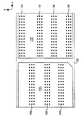
図1〜2および図4を参照すると、たとえばハウジングの内部に配置され、複数の平行した列(たとえば列1〜4)に配列された40個のコンデンサ素子を含むコンデンサアセンブリ100の特定の一実施形態を示す。ここで10個のコンデンサ素子のそれぞれの列は、ハウジングの長さL1に沿って長手方向LGに伸長している。しかし、コンデンサアセンブリの個々の要件に応じて任意の数のコンデンサ素子がそれぞれの列に存在してよく、任意の数の列を用いてよいことを理解されたい。示されるように、コンデンサアセンブリ100のハウジングは下壁123と対向する側壁124および125を含み、その間に空間526が形成され、その中に40個のコンデンサ素子20(1)〜20(40)が含まれている。下壁123ならびに側壁124および125は、上述のように金属、プラスチック、またはセラミック材料の1つまたは複数の層から形成されてよい。コンデンサ素子20(1)〜20(40)は、ハウジングの空間526の中で平行して配列されており、そのような平行配列によってコンデンサ素子20のESRの低減が助けられ、ESRの低減がコンデンサアセンブリ100の効率的に熱を放散する能力に寄与している。Referring to FIGS. 1-2 and 4, a particular embodiment of a
図4〜図6の実施形態においては、コンデンサ素子20(1)〜20(40)は、1つのコンデンサ素子(たとえばコンデンサ素子20(1))の副表面25bが、その隣のコンデンサ素子(たとえばコンデンサ素子20(2))の副表面25aに隣接して位置付けられ、これと対面するように位置合わせされている。一方、コンデンサ素子20(1)〜20(40)のそれぞれの下側主表面23b(図3参照)は、ハウジングの下壁123と対面し、以下により詳細に考察するようにめっき層を介するなどして下壁123と接しており、コンデンサ素子の対向する副表面25a、25b、27a、および27b(図3参照)よりもむしろ下側主表面23bが下壁123と接するようにコンデンサ素子20(1)〜(40)を配列することによって、ケーシングに接するコンデンサ素子20(1)〜20(40)の表面積が増大し、これがコンデンサアセンブリ100の効率的に熱を放散する能力にさらに寄与している。本発明のコンデンサアセンブリの熱を放散する能力は、(めっき層を介してケーシングに接するコンデンサ素子の下側主表面の全表面積)対(ハウジングの体積)の比として表わすことができ、約0.05mm-1を超える比は、コンデンサアセンブリの熱を放散する能力の増大に関連付けることができる。たとえば、(めっき層を介してケーシングに接するコンデンサ素子の下側主表面の全表面積)対(ハウジングの体積)の比は約0.06mm-1を超えてよく、いくつかの実施形態においては約0.06mm-1〜約0.3mm-1、たとえば、約0.065mm-1〜約0.25mm-1、たとえば約0.07mm-1〜約0.20mm-1、たとえば約0.075mm-1〜約0.15mm-1の範囲であってよい。In the embodiments of FIGS. 4 to 6, in the capacitor elements 20 (1) to 20 (40), the
上述し、図1〜図2に示すように、コンデンサアセンブリ100は、外部アノード終端部135および外部カソード終端部137を含んでもよく、これらにコンデンサ素子20(1)〜20(40)のそれぞれの下側主表面23b上のアノードリード6および固体電解質/カソードが並列に電気的に接続している。さらに、外部終端部135および137の機械的に安定な方法での形成を促進にするために、ハウジングの内部キャビティの中でリードフレームおよびめっき層を用いてもよい。たとえば図4を参照すると、コンデンサアセンブリ100は、第1の平面部分65と、それぞれのコンデンサ素子20(1)〜20(40)のアノードリード6が伸長する方向に概して直角な平面に設けられるという意味で「直立する」第2の部分67とを有するアノードリードフレームを含んでよい。このようにして、第2の部分67によってリード6の動きを制限し、使用中の表面接触および機械的安定性を強化することができる。さらに所望であれば、リード6の周囲に絶縁材料7(たとえばTeflon(商標)ワッシャ)を用いてもよい。第2の部分67は、アノードリード6に接続される実装領域(図示せず)を有してもよい。この領域は、リード6の表面接触および機械的安定性をさらに強化するために「U字形」を有してもよい。さらに、アノードリード6は、レーザー溶接、抵抗溶接、導電性接着剤、またはその他の任意の好適な方法によってアノードリードフレームの第2の部分67に接続することができる。 As described above, as shown in FIGS. 1 and 2, the
たとえば、コンデンサ素子のそれぞれの列についての第1の部分65a、65b、65c、および65dならびに40個のコンデンサ素子のそれぞれに対応する40個の第2の部分67(1)〜67(40)(簡単にするために67と表示した)を含み得るアノードリードフレームを用いて、10個のコンデンサ素子の4個の列を接続してもよい(たとえば、第2の部分67(1)〜(10)においてそれらのアノードリード6を介してアノードリードフレームに接続されているコンデンサ素子20(1)〜20(10)を含む列1;第2の部分67(11)〜67(20)においてそれらのアノードリード6を介してアノードリードフレームに接続されているコンデンサ素子20(11)〜20(20)を含む列2;第2の部分67(21)〜67(30)においてそれらのアノードリード6を介してアノードリードフレーム構成部分65cに接続されているコンデンサ素子20(21)〜20(30)を含む列3;ならびに第2の部分67(31)〜(40)においてそれらのアノードリード6を介してアノードリードフレームに接続されているコンデンサ素子20(31)〜20(40)を含む列4)。さらに、図示していないが所望であれば、コンデンサ素子20(11)〜20(20)および20(21)〜20(30)がそれらのアノードリード6が互いに対面するように位置付けられているので、列2および列3に付随するアノードリードフレームの第1の部分65bおよび65cを結合させてアノードリードフレームの単一の第1の部分としてもよい。上で考察したように、特定の一実施形態においては、それぞれのアノードリード6は、アノードリードフレームのそれぞれの第2の部分67にレーザー溶接される。しかし、これらの構成部分は抵抗溶接、導電性接着剤等によって接続できることも理解されたい。一方、特定の一実施形態においては、アノードリードフレームの第1の部分65a〜65dは、抵抗溶接によってハウジングの下壁123に接続することができる。しかし、任意の他の好適な方法、たとえば、導電性接着剤による第1の部分65a〜65dの、ハウジングの下壁123への接続を用いることもできることを理解されたい。 For example, the
さらに、アノードリードフレームの第1の部分65a〜65dおよび第2の部分67(1)〜67(40)の表面は、アノードリード6を介してコンデンサ素子20(1)〜20(40)へ、およびハウジングの下壁123への適切な接続を確実にするために、当技術分野において公知のようにニッケル、銀、金、スズ、コバルト等またはそれらの合金を電気めっきしてもよい。特定の一実施形態においては、アノードリードフレームにそれぞれニッケルおよび銀のフラッシュによって沈着させ、実装表面もスズのはんだ層をめっきしてもよい。別の実施形態においては、導電性をさらに高めるために、アノードリードフレームのベース金属層(たとえば銅合金)の上に薄い外側金属層(たとえば金)を沈着させることができる。さらに別の実施形態においては、ニッケル−鉄合金のストリップ(たとえばNILO(登録商標)ストリップ)または任意の他の好適な金属材料(図示せず)のストリップを、アノードリードフレームの第1の部分65a〜65bの下方でハウジングの下壁123の上にはんだ付けすることができる。 Further, the surfaces of the
さらに、10個のコンデンサ素子の4つの列をハウジングの下壁123に接続するために、種々の構成部分を用いてもよい(たとえば、それらの下側主表面23bにおいて下壁123に接続されているコンデンサ素子20(1)〜20(10)を含む列1;それらの下側主表面23bにおいて下壁123に接続されているコンデンサ素子20(11)〜20(20)を含む列2;それらの下側主表面23bにおいて下壁123に接続されているコンデンサ素子20(21)〜20(30)を含む列3;それらの下側主表面23bにおいて下壁123に接続されているコンデンサ素子20(31)〜20(40)を含む列4)。たとえば一実施形態においては、コンデンサ素子20(1)〜20(40)の下側主表面23bを、導電性接着剤(図示せず)を介してハウジングの下壁123に接続することができ、ここで下壁123は金属めっき層29a、29b、29c、および29dの4つの列を含む。金属めっき層29a、29b、29c、および29dは任意の好適な金属から形成することができ、特定の一実施形態においてはニッケルめっき層であってよい。 In addition, various components may be used to connect the four rows of ten capacitor elements to the
上述のように、コンデンサ素子の接着は、アノード側であろうと、カソード側であろうと、一般に、任意の種々の公知の手法、たとえば、溶接、レーザー溶接、導電性接着剤等を用いて達成できることを理解されたい。用いる場合には、導電性接着剤は樹脂組成物とともに含まれる導電性金属粒子から形成される。金属粒子は銀、銅、金、白金、ニッケル、亜鉛、ビスマス等であってよい。樹脂組成物は熱硬化性樹脂(たとえばエポキシ樹脂)、硬化剤(たとえば酸無水物)、およびカップリング剤(たとえばシランカップリング剤)を含んでよい。好適な導電性接着剤は、Osakoらの米国特許出願公開第2006/0038304号に記載されている。As mentioned above, the adhesion of the capacitor element, whether on the anode side or the cathode side, can generally be achieved using any of a variety of known techniques, such as welding, laser welding, conductive adhesives and the like. I want you to understand. When used, the conductive adhesive is formed from conductive metal particles contained with the resin composition. The metal particles may be silver, copper, gold, platinum, nickel, zinc, bismuth and the like. The resin composition may include a thermosetting resin (eg epoxy resin), a curing agent (eg acid anhydride), and a coupling agent (eg silane coupling agent). Suitable conductive adhesives are described in US Patent Application Publication No. 2006/0038304by Osako et al.
さらに図5に示すように、コンデンサアセンブリの熱を放散する能力をさらに高めるために、コンデンサアセンブリは他の構成部分を含んでよい。たとえば、コンデンサ素子20は、いくつかのコンデンサ素子20の上側主表面23aと接するy方向の金属ストリップ133およびx方向の金属ストリップ131を含む。金属材料は銅または任意の他の放熱材料であってよく、熱の放散に利用できる表面積をさらに増大させるために作用する。 Further, as shown in FIG. 5, the capacitor assembly may include other components to further enhance the ability of the capacitor assembly to dissipate heat. For example, the
ここで図6を見ると、図4〜図5に示した配列に代わる配列を有するコンデンサアセンブリ300を示す。ここでは上で定義した列1のコンデンサ素子20(1)〜20(10)および列2の20(11)〜20(20)に付随するアノードリード6は互いに対面しており、所望であれば列1および列2のアノードリードフレームの第1の部分65aおよび65bの組み合わせを結合させて単一の構成部分とすることが可能である。同様に、上で定義した列3のコンデンサ素子20(21)〜20(30)および列4の20(31)〜20(40)に付随するアノードリード6は互いに対面しており、所望であれば列3および列4のアノードリードフレームの第1の部分65cおよび65dの組み合わせを結合させて単一の構成部分とすることが可能である。さらに、上で定義した列2および列3のコンデンサ素子の上側主表面23aは互いに隣接しており、所望であればめっき層29bおよび29cの組み合わせを単一の構成部分とすることが可能である。 Looking at FIG. 6 here, a
上で考察したように、コンデンサアセンブリはアノード終端部135およびカソード終端部137を含み、これらはハウジングの外部にあり、個別のプレート、シート等から形成されている。さらに、これらの終端部は、ハウジングの下壁123を通って伸長する導電性配線を介してアノードリードフレームおよびカソードめっき層/金属ストリップ(たとえばNILO(登録商標)ストリップ)構成部分に接続することができる。図4〜図5のコンデンサ素子配列に関する図7、および図6のコンデンサ素子配列に関する図8を参照すると、アノードリードフレームの第1の部分65a〜65dおよび金属めっき層29a〜29dはコンデンサアセンブリ100のケーシングの長さL1および幅W1に伸長しているので、アノードリードフレームの第1の部分65a〜65dを外部アノード終端部135に接続する導電性配線139は、外部アノード終端部135の直上かつアノードリードフレーム構成部分の第1の部分65a〜65dの直下に配置されたケーシングの下壁123の部分を通してのみ形成され、一方金属めっき層29a〜29dを外部カソード終端部137に接続する導電性配線141は、外部カソード終端部137の直上かつ金属めっき層65a〜65dの直下のケーシングの下壁123の部分を通してのみ形成されている。言うまでもなく、本発明は所望の終端部を形成するための導電性配線の使用に決して限定されず、任意の他の好適な接続手段を用いることができる。たとえば、いくつかの実施形態においては(図示せず)、アノードリードフレームおよびカソードめっき層の部分がケーシングを通って伸長して、外部アノード終端部および外部カソード終端部を形成してもよいと理解される。As discussed above, the capacitor assembly includes an
上で考察したようにコンデンサ素子20を下壁123に接続した後、コンデンサ素子20を樹脂またはカプセル化材料で被覆してもよい。特定の一実施形態においては、カプセル化材料は熱伝導性材料であってよい。図9を参照すると、コンデンサ素子を所望の方法でコンデンサアセンブリ100のベース123に接続した後、カプセル化材料143をコンデンサ素子の周囲に配置して(図示せず)、コンデンサ素子をカプセル化材料143によって少なくとも部分的にカプセル化し、その後でカプセル化材料143を硬化させてもよい。さらに、いくつかの実施形態においては、コンデンサ素子をカプセル化材料143で完全にカプセル化してもよい。そのようにしてコンデンサ素子をカプセル化材料143でカプセル化することによって、本発明のコンデンサアセンブリの熱を放散する能力をさらに促進することができる。 After connecting the
上記のように、カプセル化材料は熱伝導性材料であってよい。熱伝導性材料は、たとえば典型的にはISO 22007−2:2014に従って決定される約1W/m・K以上、いくつかの実施形態においては約2W/m・K〜約20W/m・K、いくつかの実施形態においては約2.5W/m・K〜約10W/m・Kの熱伝導率を有する。熱伝導性であるにも関わらず、材料は一般には導電性でなく、したがってASTM D257−14に従って決定される約1×10¹²Ω・cm以上、いくつかの実施形態においては約1×10¹³Ω・cm以上、いくつかの実施形態においては約1×10¹⁴Ω・cm〜約1×10²⁰Ω・cmの比較的高い体積抵抗を有する。高い熱伝導率と低い導電率の組み合わせにより、本発明者らは、カプセル化材料がコンデンサアセンブリのハウジングに用いた場合に種々の異なった利点を提供できることを見出した。たとえば、コンデンサアセンブリを高いリップル電流に曝露した場合、熱伝導性カプセル化材料は伝熱シンクとして作用してハウジングの表面に熱を放散し、それにより冷却効率を増大し、コンデンサアセンブリの寿命を延長させることができる。カプセル化材料はまた、ASTM D570−98(2010)e−1に従って決定されるような、約1%以下、いくつかの実施形態においては約0.5%以下、いくつかの実施形態においては約0.1%以下等の低い吸湿度を示すことができる。このようにして、カプセル化材料は、ハウジング内に侵入するかもしれない水による望ましくない劣化反応を阻止することができる。As mentioned above, the encapsulating material may be a thermally conductive material. The thermally conductive material is, for example, about 1 W / m · K or higher, typically determined according to ISO 22007-2: 2014, and in some embodiments from about 2 W / m · K to about 20 W / m · K, In some embodiments, it has a thermal conductivity of about 2.5 W / m · K to about 10 W / m · K. Despite being thermally conductive, the material is generally not conductive and therefore about 1 × 10¹² Ω · cm or more, as determined according to ASTM D257-14, in some embodiments about 1 × 10¹³ It has a relatively high volume resistance of Ω · cm or more, in some embodiments from about 1 × 10¹⁴ Ω · cm to about 1 × 10²⁰ Ω · cm. The combination of high thermal conductivity and low conductivity has led us to find that the encapsulating material can offer a variety of different advantages when used in the housing of capacitor assemblies. For example, when the capacitor assembly is exposed to high ripple current, the thermally conductive encapsulating material acts as a heat transfer sink to dissipate heat to the surface of the housing, thereby increasing cooling efficiency and extending the life of the capacitor assembly. Can be made to. The encapsulating material is also about 1% or less, in some embodiments about 0.5% or less, in some embodiments about 1% or less, as determined according to ASTM D570-98 (2010) e-1. It can exhibit low moisture absorption such as 0.1% or less. In this way, the encapsulating material can prevent unwanted degradation reactions by water that may enter the housing.
所望の特性を得ることを助けるため、カプセル化材料はポリマーマトリックス中に分散した1つまたは複数の熱伝導性フィラーを含む。好適な熱伝導性フィラー材料としては、金属フィラー、たとえば、アルミニウム、銀、銅、ニッケル、鉄、コバルト等およびそれらの組み合わせ(たとえば銀で被覆した銅または銀で被覆したニッケル);金属酸化物、たとえば、酸化アルミニウム、酸化亜鉛、酸化マグネシウム等およびそれらの組み合わせ;窒化物、たとえば、窒化アルミニウム、窒化ホウ素、窒化ケイ素等およびそれらの組み合わせ;ならびに炭素フィラー、たとえば、炭化ケイ素、カーボンブラック、炭素フラーレン、グラファイトフレーク、炭素ナノチューブ、炭素ナノファイバー等およびそれらの組み合わせが挙げられる。本発明における使用には、アルミニウム、酸化亜鉛、窒化アルミニウム、窒化ホウ素、および/または炭化ケイ素粉末が特に好適であり得る。所望であれば、フィラーとポリマーマトリックスとの間の親和性を改善するために、機能性コーティングでフィラーを被覆してもよい。たとえば、そのようなコーティングとしては、不飽和または飽和脂肪酸、たとえば、アルカン酸、アルケン酸、プロピオン酸、ラウリン酸、パルミチン酸、ステアリン酸等;有機シラン、有機チタネート、有機ジルコネート、イソシアネート、ヒドロキシル末端アルケンまたはアルカン等が挙げることができる。 To help obtain the desired properties, the encapsulating material comprises one or more thermally conductive fillers dispersed in the polymer matrix. Suitable thermal conductive filler materials include metal fillers such as aluminum, silver, copper, nickel, iron, cobalt and the like and combinations thereof (eg silver coated copper or silver coated nickel); metal oxides, For example, aluminum oxide, zinc oxide, magnesium oxide and the like and combinations thereof; nitrides such as aluminum nitride, boron nitride, silicon nitride and the like and combinations thereof; and carbon fillers such as silicon carbide, carbon black, carbon fullerene, etc. Examples thereof include graphite flakes, carbon nanotubes, carbon nanofibers and the like, and combinations thereof. Aluminum, zinc oxide, aluminum nitride, boron nitride, and / or silicon carbide powder may be particularly suitable for use in the present invention. If desired, the filler may be coated with a functional coating to improve the affinity between the filler and the polymer matrix. For example, such coatings include unsaturated or saturated fatty acids such as alkanoic acid, alkenes, propionic acids, lauric acid, palmitic acid, stearic acid; organic silanes, organic titanates, organic zirconates, isocyanates, hydroxyl-terminated alkanes. Alternatively, alkanes and the like can be mentioned.
本発明においては熱伝導性フィラーの寸法は、所望の特性を達成することを助けるために選択的に制御し得る。一般論で言えば、そのようなフィラーは約10nm〜約75μm、いくつかの実施形態においては約15nm〜約50μm、いくつかの実施形態においては約20nm〜約40μmの平均寸法(たとえば直径)を有する。いくつかの実施形態においては、フィラーはナノスケール寸法、たとえば、約10nm〜約500nm、いくつかの実施形態においては約20nm〜約350nm、いくつかの実施形態においては約50nm〜約200nmを有し得る。一方他の実施形態においては、フィラーは約1μm〜約50μm、いくつかの実施形態においては、フィラーは、ミクロンスケール寸法、たとえば、約2μm〜約30μm、いくつかの実施形態においては約5μm〜約15μmを有し得る。カプセル化材料にも、ナノスケールおよびミクロンスケールの両方の熱伝導性フィラーの組み合わせを用いてよい。そのような実施形態においては、ミクロンスケールのフィラー対ナノスケールのフィラーの寸法を有する粒子の比は、高充填密度を確実にするために、約50:1以上、いくつかの実施形態においては約70:1〜約150:1と、比較的大きくてよい。 In the present invention, the dimensions of the thermally conductive filler can be selectively controlled to help achieve the desired properties. Generally speaking, such fillers have an average dimension (eg, diameter) of about 10 nm to about 75 μm, in some embodiments about 15 nm to about 50 μm, and in some embodiments about 20 nm to about 40 μm. Have. In some embodiments, the filler has nanoscale dimensions such as from about 10 nm to about 500 nm, in some embodiments from about 20 nm to about 350 nm, and in some embodiments from about 50 nm to about 200 nm. obtain. On the other hand, in other embodiments, the filler is from about 1 μm to about 50 μm, in some embodiments the filler has micron scale dimensions, eg, about 2 μm to about 30 μm, and in some embodiments about 5 μm to about. It can have 15 μm. The encapsulation material may also be a combination of both nanoscale and micron scale thermally conductive fillers. In such embodiments, the ratio of particles with micron-scale filler to nanoscale filler dimensions is greater than or equal to about 50: 1 to ensure high packing density, and in some embodiments about. It may be relatively large, 70: 1 to about 150: 1.
カプセル化材料のマトリックスにおいては種々の異なったポリマー樹脂を用い得るが、本発明における使用には硬化可能な熱硬化性樹脂が特に好適であることが見出された。そのような樹脂の例としては、たとえばシリコーンポリマー、ビスフェノールAジグリシジルエーテルのポリマー、アクリレートポリマー、ウレタンポリマー等が挙げられる。たとえばある実施形態においては、カプセル化材料として1つまたは複数のポリオルガノシロキサンを用い得る。これらのポリマーにおいて用いられるケイ素結合有機基には、1価の炭化水素および/または1価のハロゲン化炭化水素基が含まれ得る。そのような1価の基は、典型的には1〜約20個の炭素原子、好ましくは1〜10個の炭素原子を有し、これだけに限らないがアルキル(たとえばメチル、エチル、プロピル、ペンチル、オクチル、ウンデシル、およびオクタデシル);シクロアルキル(たとえばシクロヘキシル);アルケニル(たとえばビニル、アリル、ブテニル、およびヘキセニル);アリール(たとえばフェニル、トリル、キシリル、ベンジル、および2−フェニルエチル);およびハロゲン化炭化水素基(たとえば3,3,3−トリフルオロプロピル、3−クロロプロピル、およびジクロロフェニル)が例示される。典型的には、有機基の少なくとも50%、より望ましくは少なくとも80%がメチルである。そのようなメチルポリシロキサンの例としては、たとえばポリジメチルシロキサン(「PDMS」)、ポリメチルハイドロジェンシロキサン等が挙げることができる。さらに他の好適なメチルポリシロキサンとしては、ジメチルジフェニルポリシロキサン、ジメチル/メチルフェニルポリシロキサン、ポリメチルフェニルシロキサン、メチルフェニル/ジメチルシロキサン、ビニルジメチル末端ポリジメチルシロキサン、ビニルメチル/ジメチルポリシロキサン、ビニルジメチル末端ビニルメチル/ジメチルポリシロキサン、ジビニルメチル末端ポリジメチルシロキサン、ビニルフェニルメチル末端ポリジメチルシロキサン、ジメチルヒドロ末端ポリジメチルシロキサン、メチルヒドロ/ジメチルポリシロキサン、メチルヒドロ末端メチルオクチルポリシロキサン、メチルヒドロ/フェニルメチルポリシロキサン等が挙げることができる。 Although a variety of different polymeric resins can be used in the matrix of encapsulating materials, it has been found that curable thermosetting resins are particularly suitable for use in the present invention. Examples of such resins include silicone polymers, bisphenol A diglycidyl ether polymers, acrylate polymers, urethane polymers and the like. For example, in certain embodiments, one or more polyorganosiloxanes may be used as the encapsulation material. The silicon-bonded organic groups used in these polymers may include monovalent hydrocarbons and / or monovalent halogenated hydrocarbon groups. Such monovalent groups typically have 1 to about 20 carbon atoms, preferably 1 to 10 carbon atoms, and are not limited to alkyl (eg, methyl, ethyl, propyl, pentyl, etc.). , Octyl, undecyl, and octadecyl); cycloalkyl (eg cyclohexyl); alkenyl (eg vinyl, allyl, butenyl, and hexenyl); aryl (eg phenyl, trill, xsilyl, benzyl, and 2-phenylethyl); and halogenated Hydrocarbon groups (eg, 3,3,3-trifluoropropyl, 3-chloropropyl, and dichlorophenyl) are exemplified. Typically, at least 50%, more preferably at least 80% of the organic groups are methyl. Examples of such methylpolysiloxane include polydimethylsiloxane (“PDMS”), polymethylhydrogensiloxane, and the like. Still other suitable methylpolysiloxanes include dimethyldiphenylpolysiloxane, dimethyl / methylphenylpolysiloxane, polymethylphenylsiloxane, methylphenyl / dimethylsiloxane, vinyldimethyl-terminated polydimethylsiloxane, vinylmethyl / dimethylpolysiloxane, vinyldimethyl. Terminal vinylmethyl / dimethylpolysiloxane, divinylmethyl-terminal polydimethylsiloxane, vinylphenylmethyl-terminal polydimethylsiloxane, dimethylhydro-terminal polydimethylsiloxane, methylhydro / dimethylpolysiloxane, methylhydro-terminal methyloctylpolysiloxane, methylhydro / phenylmethylpolysiloxane, etc. Can be mentioned.
オルガノポリシロキサンは、ある程度の親水性をポリマーに付与する1つまたは複数のペンダントおよび/または末端の極性官能基、たとえば、ヒドロキシル、エポキシ、カルボキシル、アミノ、アルコキシ、メタクリル、またはメルカプト基を含んでいてもよい。たとえば、オルガノポリシロキサンは分子あたり少なくとも1つのヒドロキシ基を含み、平均して少なくとも2つのケイ素結合ヒドロキシ基(シラノール基)を含んでもよい。そのようなオルガノポリシロキサンの例としては、たとえばジヒドロキシポリジメチルシロキサン、ヒドロキシトリメチルシロキシポリジメチルシロキサン等が挙げられる。アルコキシ改質オルガノポリシロキサン、たとえば、ジメトキシポリジメチルシロキサン、メトキシトリメチルシロキシポリジメチルシロキサン、ジエトキシポリジメチルシロキサン、エトキシトリメチルシロキシポリジメチルシロキサン等も用い得る。さらに他の好適なオルガノポリシロキサンは、少なくとも1つのアミノ官能基で改質したものである。そのようなアミノ官能性ポリシロキサンの例としては、たとえばジアミノ官能性ポリジメチルシロキサンが挙げられる。 Organopolysiloxanes contain one or more pendant and / or terminal polar functional groups that impart some degree of hydrophilicity to the polymer, such as hydroxyl, epoxy, carboxyl, amino, alkoxy, methacryl, or mercapto groups. May be good. For example, an organopolysiloxane may contain at least one hydroxy group per molecule and, on average, at least two silicon-bonded hydroxy groups (silanol groups). Examples of such an organopolysiloxane include dihydroxypolydimethylsiloxane, hydroxytrimethylsiloxypolydimethylsiloxane and the like. Alkoxy-modified organopolysiloxanes, such as dimethoxypolydimethylsiloxane, methoxytrimethylsiloxypolydimethylsiloxane, diethoxypolydimethylsiloxane, ethoxytrimethylsiloxypolydimethylsiloxane, and the like can also be used. Yet another suitable organopolysiloxane is modified with at least one amino functional group. Examples of such amino-functional polysiloxanes include diamino-functional polydimethylsiloxanes.
望ましくは、硬化前のカプセル化材料の粘度および流動特性を改善するため、オルガノポリシロキサンは比較的低い分子量を有する。たとえば一実施形態においては、オルガノポリシロキサン(たとえばポリジメチルシロキサン)は、約100,000g/モル以下、いくつかの実施形態においては約60,000g/モル以下、いくつかの実施形態においては約5,000〜約30,000g/モルの分子量を有する。その結果、ギャップ0.5mmに設定された20mmの平行プレートを備えたARES R550PS応力制御レオメーターを用いて温度25℃で決定されるようなカプセル化材料の粘度(硬化前)は、たとえば約500Pa・秒以下、いくつかの実施形態においては約100Pa・秒以下、いくつかの実施形態においては約1〜約50Pa・秒であり得る。 Desirably, the organopolysiloxane has a relatively low molecular weight in order to improve the viscosity and flow properties of the encapsulating material before curing. For example, in one embodiment, the organopolysiloxane (eg, polydimethylsiloxane) is about 100,000 g / mol or less, in some embodiments about 60,000 g / mol or less, and in some embodiments about 5 It has a molecular weight of 000 to about 30,000 g / mol. As a result, the viscosity (before curing) of the encapsulating material, as determined at a temperature of 25 ° C. using an ARES R550PS stress control rheometer with a 20 mm parallel plate set to a gap of 0.5 mm, is, for example, about 500 Pa. It can be less than a second, about 100 Pa · seconds or less in some embodiments, and about 1 to about 50 Pa · seconds in some embodiments.
熱伝導性フィラーとポリマーマトリックスの相対量は、所望の特性が達成されるように選択的に制御し得る。たとえば、カプセル化材料は典型的には約25体積%〜約95体積%、いくつかの実施形態においては約40体積%〜約90体積%、いくつかの実施形態においては約50体積%〜約85体積%を含む。同様に、ポリマーマトリックスは材料の約5体積%〜約75体積%、いくつかの実施形態においては約10体積%〜約50体積%、いくつかの実施形態においては約15体積%〜約40体積%を構成する。所望であれば、他の添加剤、たとえば、相溶化剤、硬化剤、光開始剤、粘度調整剤、顔料、カップリング剤(たとえばシランカップリング剤)、安定剤等をカプセル化材料中に用いてもよい。 The relative amounts of the thermally conductive filler and the polymer matrix can be selectively controlled to achieve the desired properties. For example, the encapsulating material is typically from about 25% to about 95% by volume, in some embodiments from about 40% to about 90% by volume, and in some embodiments from about 50% to about 50% by volume. Contains 85% by volume. Similarly, the polymer matrix is about 5% to about 75% by volume of the material, about 10% to about 50% by volume in some embodiments, and about 15% to about 40% by volume in some embodiments. Consists of%. If desired, other additives such as compatibilizers, hardeners, photoinitiators, viscosity modifiers, pigments, coupling agents (eg silane coupling agents), stabilizers and the like are used in the encapsulating material. You may.
所望の方法によっていったん組み立てて接続すれば、得られるパッケージを上述のように密閉シールする。再び図1を参照し、たとえばコンデンサ素子をハウジング内に位置付けた後、ハウジングには側壁124および125の上面に設けた蓋127を含めてもよい。蓋はセラミック、金属(たとえば鉄、銅、ニッケル、コバルト等、ならびにそれらの合金)、プラスチック等から形成してよい。所望であれば、シールを良好にするために閉鎖部材(図示せず)を蓋と側壁124および125との間に配置してもよい。たとえば一実施形態においては、閉鎖部材としてはガラス−金属のシール、Kovar(登録商標)リング(Goodfellow Camridge,Ltd.)等が挙げられる。側壁の高さは一般に、蓋がコンデンサ素子のいずれの表面にも接触せず、それゆえそれらが汚染されないような高さである。所望の位置に設置した場合、公知の手法、たとえば、溶接(たとえば抵抗溶接、レーザー溶接等)、はんだ付け等を用いて、蓋を側壁124および125に密閉シールする。いくつかの実施形態においては、密閉シールは上述のように不活性ガスの存在下に行なわれ、したがって得られるアセンブリには、反応性ガス、たとえば、酸素または水蒸気が実質的に存在しない。
図4〜図6に示す実施形態においては、コンデンサアセンブリは40個のコンデンサ素子を含む。しかし上記のように、本発明においては一般に、約2〜約200、いくつかの実施形態においては約10〜約100、いくつかの実施形態においては約20〜約50の、任意の数のコンデンサ素子が用いられる。Once assembled and connected by the desired method, the resulting package is hermetically sealed as described above. With reference to FIG. 1 again, for example, after positioning the capacitor element in the housing, the housing may include a
In the embodiments shown in FIGS. 4-6, the capacitor assembly comprises 40 capacitor elements. However, as described above, in the present invention, there are generally any number of capacitors of about 2 to about 200, some embodiments of about 10 to about 100, and some embodiments of about 20 to about 50. The element is used.
その個々の構成に関わらず、本発明のコンデンサアセンブリは、高電圧環境および高温に曝露された場合においても、優れた電気特性を示し得る。たとえば、本発明のコンデンサアセンブリの熱を放散する能力により、コンデンサアセンブリを損傷することなく、比較的高いリップル電流を達成し得る。たとえば、最大リップル電流は約25アンペア以上、いくつかの実施形態においては約50アンペア以上、いくつかの実施形態においては約75アンペア以上であり得る。さらに、コンデンサアセンブリの等価直列抵抗(ESR)は約50mΩ未満、いくつかの実施形態においては約25mΩ未満、いくつかの実施形態においては約10mΩ未満であり得る。たとえば、ESRは約0.5mΩ〜約10mΩ、たとえば、約1mΩ〜約8mΩ、たとえば約2mΩ〜約6mΩの範囲であり得る。 Regardless of their individual configuration, the capacitor assemblies of the present invention may exhibit excellent electrical properties even when exposed to high voltage environments and high temperatures. For example, the ability of the capacitor assembly of the present invention to dissipate heat allows a relatively high ripple current to be achieved without damaging the capacitor assembly. For example, the maximum ripple current can be about 25 amps or more, in some embodiments about 50 amps or more, and in some embodiments about 75 amps or more. In addition, the equivalent series resistance (ESR) of a capacitor assembly can be less than about 50 mΩ, less than about 25 mΩ in some embodiments, and less than about 10 mΩ in some embodiments. For example, the ESR can range from about 0.5 mΩ to about 10 mΩ, for example from about 1 mΩ to about 8 mΩ, for example from about 2 mΩ to about 6 mΩ.
本発明は以下の例を参照することによって、より良く理解できる。
試験手順
等価直列抵抗(ESR)
等価直列抵抗は、ケルビンリードを備えたAgilent E4980A Precision LCR Meterを用いて、DCバイアスを2.2V、ピークツーピーク正弦波信号を0.5Vとして測定することができる。動作周波数は100kHz、温度は23℃±2℃であった。The present invention can be better understood by referring to the following examples.
Test procedure Equivalent series resistance (ESR)
The equivalent series resistance can be measured using an Agilent E4980A Precision LCR Meter with Kelvin leads, with a DC bias of 2.2V and a peak-to-peak sinusoidal signal of 0.5V. The operating frequency was 100 kHz and the temperature was 23 ° C ± 2 ° C.
キャパシタンス(CAP)
キャパシタンスは、ケルビンリードを備えたAgilent E4980A Precision LCR Meterを用いて、DCバイアスを2.2V、ピークツーピーク正弦波信号を0.5Vとして測定した。動作周波数は120Hzであった。
漏洩電流(DCL)
漏洩電流は、漏洩電流を測定するKeithley 2410 Source Meterを用いて、最小60秒後に適切な電圧(25℃〜85℃についてはUr、125℃についてはUrの60%、および150℃についてはUrの50%)で用いて測定した。Capacitance (CAP)
Capacitance was measured using an Agilent E4980A Precision LCR Meter with Kelvin leads, with a DC bias of 2.2V and a peak-to-peak sinusoidal signal of 0.5V. The operating frequency was 120 Hz.
Leakage current (DCL)
Leakage current is measured at a minimum of 60 seconds using a Keithley 2410 Source Meter that measures the leakage current and is at the appropriate voltage (Ur for 25 ° C to 85 ° C, 60% of Ur for 125 ° C, and Ur for 150 ° C. 50%) was used and measured.
リップル電流
リップル電流は、GoldStar GP505電源、Agilent 33210A信号発生器、Pt100熱電対を備えたAlmemo 2590−9データロガー、およびFluke 80iオシロスコープを用いて測定した。適切な値のリップル電流がコンデンサを通過する場合、AC信号および10VのDCバイアスに関して動作周波数は20kHzであった。リップル電流の増大とともに温度も上昇した。温度はサーモカメラでモニターした。Ripple Current Ripple current was measured using a GoldStar GP505 power supply, an Agilent 33210A signal generator, an Almemo 2590-9 data logger with a Pt100 thermocouple, and a Fluke 80i oscilloscope. The operating frequency was 20 kHz with respect to the AC signal and 10 V DC bias when a properly valued ripple current passed through the capacitor. As the ripple current increased, so did the temperature. The temperature was monitored with a thermo camera.
9,000μFV/gのタンタル粉末を用いてアノード試料を形成した。それぞれのアノード試料をタンタルワイヤに埋め込み、1800℃で焼結し、密度5.3g/cm3にプレスした。得られたペレットの寸法は4.6mm×5.25mm×2.6mmであった。温度85℃で、導電率8.6mSの水/リン酸電解質中でペレットを260Vに電解酸化して誘電体層を形成した。次いでアノードを、固体含量が1.1%、粘度が20mPa・秒のポリ(3,4−エチレンジオキシチオフェン)(Clevios(商標)K、H.C.Starck)の分散液に浸漬することによって、導電性ポリマーコーティングを形成した。コーティングに際して、部品を125℃で20分乾燥した。このプロセスを10回繰り返した。その後、部品を固体含量2%、粘度20mPa・秒のポリ(3,4−エチレンジオキシチオフェン)(Clevios(商標)K、H.C.Starck)の分散液に浸漬した。コーティングに際して、部品を125℃で20分乾燥した。このプロセスは繰り返さなかった。次に、部品を固体含量2%、粘度160mPa・秒のポリ(3,4−エチレンジオキシチオフェン)(Clevios(商標)K、H.C.Starck)の分散液に浸漬した。コーティングに際して、部品を125℃で20分乾燥した。このプロセスを8回繰り返した。次いで部品をグラファイト分散液に浸漬して、乾燥した。最後に、部品を銀の分散液に浸漬して、乾燥した。このようにして、100Vコンデンサの複数の部品を作成した。
銅ベースリードフレーム材料を用いてアセンブリプロセスを完了し、コンデンサ素子をセラミックハウジング内に設置した。コンデンサアセンブリは並列に接続した4列(1列あたりコンデンサ素子9個)、36個のコンデンサ素子を含んでいた。次いでカソード接続部材をニッケルのカソード終端部に接着し、長さ58.0mm、幅35.0mm、厚さ5.45mmのセラミックハウジングの下壁でアノードリードフレームをニッケルアノード終端部に溶接した。ハウジングは、セラミックハウジングの下壁の内表面にはんだ付けしたニッケルめっきNILO(登録商標)はんだパッドを有していた。An anode sample was formed using 9,000 μFV / g tantalum powder. Each anode sample was embedded in tantalum wire, sintered at 1800 ° C. and pressed to adensity of 5.3 g / cm 3. The dimensions of the obtained pellets were 4.6 mm × 5.25 mm × 2.6 mm. At a temperature of 85 ° C., the pellet was electrolytically oxidized to 260 V in a water / phosphoric acid electrolyte having a conductivity of 8.6 mS to form a dielectric layer. The anode is then immersed in a dispersion of poly (3,4-ethylenedioxythiophene) (Clevios ™ K, HC Stark) with a solid content of 1.1% and a viscosity of 20 mPa · sec. , Formed a conductive polymer coating. Upon coating, the parts were dried at 125 ° C. for 20 minutes. This process was repeated 10 times. Then, the parts were immersed in a dispersion of poly (3,4-ethylenedioxythiophene) (Clevios ™ K, HC Starck) having a solid content of 2% and a viscosity of 20 mPa · sec. Upon coating, the parts were dried at 125 ° C. for 20 minutes. This process was not repeated. The component was then immersed in a dispersion of poly (3,4-ethylenedioxythiophene) (Clevios ™ K, HC Starck) with a solid content of 2% and a viscosity of 160 mPa · sec. Upon coating, the parts were dried at 125 ° C. for 20 minutes. This process was repeated 8 times. The parts were then immersed in a graphite dispersion and dried. Finally, the parts were dipped in a silver dispersion and dried. In this way, a plurality of parts of the 100V capacitor were created.
The assembly process was completed using copper-based lead frame material and the capacitor elements were placed inside the ceramic housing. The capacitor assembly contained 36 capacitor elements in 4 rows (9 capacitor elements per row) connected in parallel. The cathode connecting member was then glued to the nickel cathode termination and the anode lead frame was welded to the nickel anode termination on the lower wall of a ceramic housing 58.0 mm long, 35.0 mm wide and 5.45 mm thick. The housing had a nickel-plated NILO® solder pad soldered to the inner surface of the lower wall of the ceramic housing.
全ての接続に用いた接着剤は銀ペーストであった。次いでアセンブリを対流オーブンに装入してペーストをはんだ付けした。その後、アノード接続のために用いた溶接は、リードフレーム部分とセラミックハウジングのニッケルめっきはんだパッドとの間に100ミリ秒印加した300Wのエネルギーを用いた抵抗溶接であった。次いで、コンデンサ素子のアノードおよびカソード部分の上部に熱伝導性シリコーンカプセル化剤(Thermoset SC−320)を塗布し、150℃で24時間乾燥した。次に、ハウジングの上部に、セラミックのシールリングにしっかりと、Kovar(登録商標)蓋を取り付けた。得られたアセンブリを溶接チャンバーに入れ、窒素ガスをパージして、シールリングと蓋との間のシーム溶接を行なった。 The adhesive used for all connections was silver paste. The assembly was then placed in a convection oven and the paste was soldered. After that, the welding used for the anode connection was resistance welding using 300 W of energy applied for 100 milliseconds between the lead frame portion and the nickel-plated solder pad of the ceramic housing. Next, a thermosetting silicone encapsulating agent (Thermodet SC-320) was applied to the upper part of the anode and cathode portions of the capacitor element, and dried at 150 ° C. for 24 hours. The Kovar® lid was then firmly attached to the ceramic seal ring on top of the housing. The resulting assembly was placed in a welding chamber, purged with nitrogen gas and seam welded between the seal ring and the lid.
試験の後、キャパシタンスが340.1μF、ESRが4.3mΩと決定した。漏洩電流およびリップル電流の試験結果の概要を以下に示す。 After the test, the capacitance was determined to be 340.1 μF and the ESR was determined to be 4.3 mΩ. The outline of the test results of leakage current and ripple current is shown below.
当業者であれば、本発明の精神および範囲から逸脱することなく、本発明のこれらのおよびその他の変更および変形を実施することができよう。さらに、種々の実施形態の態様は、全体としてまたは部分的に、相互変換可能であり得ることを理解されたい。さらに、当業者であれば、上記の説明は例としてのみであって、添付した特許請求の範囲にさらに記載した発明を限定する意図はないことが理解されよう。
Those skilled in the art will be able to implement these and other modifications and variations of the invention without departing from the spirit and scope of the invention. Further, it should be understood that aspects of the various embodiments may be interchangeable, in whole or in part. Further, those skilled in the art will appreciate that the above description is merely an example and is not intended to limit the invention further described in the appended claims.
6 アノードリード
7 絶縁材料
20 コンデンサ素子
23 主表面
25 第1の副表面
27 第2の副表面
29 金属めっき層
65 第1の平面部分
67 第2の部分
100 コンデンサアセンブリ
123 下壁
124 側壁
125 側壁
127 蓋
131 x方向の金属ストリップ
133 y方向の金属ストリップ
135 外部アノード終端部
137 外部カソード終端部
139 導電性配線
141 導電性配線
143 カプセル化材料
200 コンデンサアセンブリ
300 コンデンサアセンブリ
526 空間
H ハウジングの高さ
L ハウジングの長さ
W ケーシングの幅
LG 長手方向6
Claims (20)
Translated fromJapanese長さ、幅および高さを有するハウジングであって、長さ対高さの比が約2〜約80の範囲であり、前記ハウジングが密閉シールされ、前記複数のコンデンサ素子が内部に位置付けられている内部キャビティを画定しており、それぞれのコンデンサ素子の下側主表面が前記ハウジングの下壁と対面し、さらに前記下壁が前記ハウジングの長さおよび幅によって画定されている、ハウジングと、
それぞれのコンデンサ素子の前記アノードリードと電気的に接続されている外部アノード終端部と、
それぞれのコンデンサ素子の前記固体電解質と電気的に接続されている外部カソード終端部と
を含む、コンデンサアセンブリ。A plurality of capacitor elements, each containing a sintered porous anode body, a dielectric layer covering the anode body, and a solid electrolyte covering the dielectric layer, and an anode lead extending from each capacitor element, respectively. Capacitor elements are defined by an upper and lower main surface, a first opposing subsurface, and a second opposing subsurface, with the upper and lower main surfaces facing each other, respectively. With multiple capacitor elements, which have a surface area greater than the surface area of
A housing having length, width and height with a length-to-height ratio in the range of about 2 to about 80, the housing being hermetically sealed and the plurality of capacitor elements positioned internally. A housing in which the lower main surface of each capacitor element faces the lower wall of the housing, and the lower wall is further defined by the length and width of the housing.
An external anode termination that is electrically connected to the anode lead of each capacitor element,
A capacitor assembly that includes said solid electrolyte of each capacitor element and an external cathode termination that is electrically connected.
Applications Claiming Priority (2)
| Application Number | Priority Date | Filing Date | Title |
|---|---|---|---|
| US14/657,194 | 2015-03-13 | ||
| US14/657,194US10014108B2 (en) | 2015-03-13 | 2015-03-13 | Low profile multi-anode assembly |
Related Parent Applications (1)
| Application Number | Title | Priority Date | Filing Date |
|---|---|---|---|
| JP2016048711ADivisionJP6881894B2 (en) | 2015-03-13 | 2016-03-11 | Thin multi-anode assembly |
Publications (1)
| Publication Number | Publication Date |
|---|---|
| JP2021093544Atrue JP2021093544A (en) | 2021-06-17 |
Family
ID=56800753
Family Applications (2)
| Application Number | Title | Priority Date | Filing Date |
|---|---|---|---|
| JP2016048711AActiveJP6881894B2 (en) | 2015-03-13 | 2016-03-11 | Thin multi-anode assembly |
| JP2021031406AAbandonedJP2021093544A (en) | 2015-03-13 | 2021-03-01 | Low profile multi-anode assembly |
Family Applications Before (1)
| Application Number | Title | Priority Date | Filing Date |
|---|---|---|---|
| JP2016048711AActiveJP6881894B2 (en) | 2015-03-13 | 2016-03-11 | Thin multi-anode assembly |
Country Status (4)
| Country | Link |
|---|---|
| US (1) | US10014108B2 (en) |
| JP (2) | JP6881894B2 (en) |
| CN (1) | CN105977036B (en) |
| DE (1) | DE102016202779A1 (en) |
Families Citing this family (5)
| Publication number | Priority date | Publication date | Assignee | Title |
|---|---|---|---|---|
| CN108369867A (en)* | 2015-12-18 | 2018-08-03 | 凯米特电子公司 | Capacitor with package thickness control by film and manufacturing method |
| WO2019005535A1 (en) | 2017-06-29 | 2019-01-03 | Avx Corporation | Module containing hermetically sealed capacitors |
| TWI787326B (en) | 2017-09-08 | 2022-12-21 | 日商杜邦東麗特殊材料股份有限公司 | Manufacturing method of sealed optical semiconductor element |
| TWI779077B (en) | 2017-09-08 | 2022-10-01 | 日商杜邦東麗特殊材料股份有限公司 | Manufacturing method of encapsulated photo-semiconductor element |
| US11126248B2 (en) | 2019-06-25 | 2021-09-21 | Western Digital Technologies, Inc. | Data storage device detecting supply current limit |
Family Cites Families (131)
| Publication number | Priority date | Publication date | Assignee | Title |
|---|---|---|---|---|
| US3345545A (en) | 1964-11-27 | 1967-10-03 | Johnson Matthey & Mallory Ltd | Solid electrolytic capacitor having minimum anode impedance |
| GB1069685A (en) | 1965-08-31 | 1967-05-24 | Mallory & Co Inc P R | Atmosphere control within the hermetic enclosure of electrolytic-capacitor assemblies |
| US3611055A (en) | 1970-04-24 | 1971-10-05 | Sprague Electric Co | Solid electrolyte capacitor |
| US4085435A (en) | 1976-06-14 | 1978-04-18 | Avx Corporation | Tantalum chip capacitor |
| US3922773A (en) | 1974-07-17 | 1975-12-02 | Corning Glass Works | Method of forming a hermetic enclosure |
| US4017302A (en) | 1976-02-04 | 1977-04-12 | Fansteel Inc. | Tantalum metal powder |
| US4107762A (en) | 1977-05-16 | 1978-08-15 | Sprague Electric Company | Solid electrolyte capacitor package with an exothermically-alloyable fuse |
| DE3130392C2 (en) | 1981-07-31 | 1985-10-17 | Hermann C. Starck Berlin, 1000 Berlin | Process for the production of pure agglomerated valve metal powder for electrolytic capacitors, their use and process for the production of sintered anodes |
| US4441927A (en) | 1982-11-16 | 1984-04-10 | Cabot Corporation | Tantalum powder composition |
| US4479168A (en) | 1983-12-19 | 1984-10-23 | Sprague Electric Company | Electrolytic capacitor with a hermetic seal |
| US4555268A (en) | 1984-12-18 | 1985-11-26 | Cabot Corporation | Method for improving handling properties of a flaked tantalum powder composition |
| US4755908A (en) | 1987-08-17 | 1988-07-05 | Gardner Edward P | Capacitor |
| DE3843412A1 (en) | 1988-04-22 | 1990-06-28 | Bayer Ag | NEW POLYTHIOPHENES, METHOD FOR THEIR PRODUCTION AND THEIR USE |
| DE3814730A1 (en) | 1988-04-30 | 1989-11-09 | Bayer Ag | SOLID ELECTROLYTE AND ELECTROLYTE CONDENSERS CONTAINING THEM |
| US5082491A (en) | 1989-09-28 | 1992-01-21 | V Tech Corporation | Tantalum powder with improved capacitor anode processing characteristics |
| US4945452A (en) | 1989-11-30 | 1990-07-31 | Avx Corporation | Tantalum capacitor and method of making same |
| EP0440957B1 (en) | 1990-02-08 | 1996-03-27 | Bayer Ag | New polythiophene dispersions, their preparation and their use |
| JPH03127813U (en) | 1990-04-09 | 1991-12-24 | ||
| US5111327A (en) | 1991-03-04 | 1992-05-05 | General Electric Company | Substituted 3,4-polymethylenedioxythiophenes, and polymers and electro responsive devices made therefrom |
| US5198968A (en) | 1992-07-23 | 1993-03-30 | Avx Corporation | Compact surface mount solid state capacitor and method of making same |
| US5357399A (en) | 1992-09-25 | 1994-10-18 | Avx Corporation | Mass production method for the manufacture of surface mount solid state capacitor and resulting capacitor |
| US5314606A (en) | 1993-02-16 | 1994-05-24 | Kyocera America, Inc. | Leadless ceramic package with improved solderabilty |
| US5394295A (en) | 1993-05-28 | 1995-02-28 | Avx Corporation | Manufacturing method for solid state capacitor and resulting capacitor |
| JP2765462B2 (en) | 1993-07-27 | 1998-06-18 | 日本電気株式会社 | Solid electrolytic capacitor and method of manufacturing the same |
| US5495386A (en) | 1993-08-03 | 1996-02-27 | Avx Corporation | Electrical components, such as capacitors, and methods for their manufacture |
| JPH07135126A (en) | 1993-11-10 | 1995-05-23 | Nec Corp | Solid electrolytic capacitor and its manufacture |
| JP3070408B2 (en) | 1993-12-28 | 2000-07-31 | 日本電気株式会社 | Solid electrolytic capacitor and method of manufacturing the same |
| US5638253A (en) | 1994-04-28 | 1997-06-10 | Rohm Co. Ltd. | Package-type solid electrolytic capacitor |
| JP2770746B2 (en) | 1994-09-02 | 1998-07-02 | 日本電気株式会社 | Solid electrolytic capacitor and method of manufacturing the same |
| JP2778495B2 (en) | 1994-12-28 | 1998-07-23 | 日本電気株式会社 | Heat-resistant conductive polymer, solid electrolytic capacitor using the conductive polymer, and method of manufacturing the same |
| US5608261A (en) | 1994-12-28 | 1997-03-04 | Intel Corporation | High performance and high capacitance package with improved thermal dissipation |
| JP3068430B2 (en) | 1995-04-25 | 2000-07-24 | 富山日本電気株式会社 | Solid electrolytic capacitor and method of manufacturing the same |
| JP3127813B2 (en) | 1995-12-05 | 2001-01-29 | ヤマハ株式会社 | Audio amplifier protection circuit |
| US5812367A (en) | 1996-04-04 | 1998-09-22 | Matsushita Electric Industrial Co., Ltd. | Solid electrolytic capacitors comprising a conductive layer made of a polymer of pyrrole or its derivative |
| US5954856A (en) | 1996-04-25 | 1999-09-21 | Cabot Corporation | Method of making tantalum metal powder with controlled size distribution and products made therefrom |
| JP3863232B2 (en) | 1996-09-27 | 2006-12-27 | ローム株式会社 | Structure of capacitor element used for solid electrolytic capacitor and method of compacting chip body in capacitor element |
| GB9700566D0 (en) | 1997-01-13 | 1997-03-05 | Avx Ltd | Binder removal |
| KR100522066B1 (en) | 1997-02-19 | 2005-10-18 | 하.체. 스타르크 게엠베하 | Tantalum Powder, Method for Producing Same Powder and Sintered Anodes Obtained From It |
| TW388043B (en) | 1997-04-15 | 2000-04-21 | Sanyo Electric Co | Solid electrolyte capacitor |
| JPH11112157A (en) | 1997-09-30 | 1999-04-23 | Kyocera Corp | Electronic component case, electronic component and electrolytic capacitor using the same |
| US6576038B1 (en) | 1998-05-22 | 2003-06-10 | Cabot Corporation | Method to agglomerate metal particles and metal particles having improved properties |
| JP2000058401A (en) | 1998-08-14 | 2000-02-25 | Rohm Co Ltd | Solid electrolytic capacitor |
| US6416730B1 (en) | 1998-09-16 | 2002-07-09 | Cabot Corporation | Methods to partially reduce a niobium metal oxide oxygen reduced niobium oxides |
| US6322912B1 (en) | 1998-09-16 | 2001-11-27 | Cabot Corporation | Electrolytic capacitor anode of valve metal oxide |
| US6391275B1 (en) | 1998-09-16 | 2002-05-21 | Cabot Corporation | Methods to partially reduce a niobium metal oxide and oxygen reduced niobium oxides |
| JP3403103B2 (en) | 1998-12-21 | 2003-05-06 | 三洋電機株式会社 | Solid electrolytic capacitors |
| US6191936B1 (en) | 1999-04-12 | 2001-02-20 | Vishay Sprague, Inc. | Capacitor having textured pellet and method for making same |
| JP3942000B2 (en) | 1999-06-01 | 2007-07-11 | ローム株式会社 | Structure of package type solid electrolytic capacitor and manufacturing method thereof |
| DE10004725A1 (en) | 2000-02-03 | 2001-08-09 | Bayer Ag | Process for the preparation of water-soluble pi-conjugated polymers |
| JP3959220B2 (en) | 2000-02-04 | 2007-08-15 | 株式会社エスアイアイ・マイクロパーツ | Non-aqueous electrolytic battery for surface mounting and electric double layer capacitor for surface mounting |
| US6576099B2 (en) | 2000-03-23 | 2003-06-10 | Cabot Corporation | Oxygen reduced niobium oxides |
| DE10016723A1 (en) | 2000-04-04 | 2001-10-11 | Bayer Ag | Process for the preparation of dialkoxythiophenes and alkylenedioxythiophenes |
| DE10029075A1 (en) | 2000-06-13 | 2001-12-20 | Bayer Ag | Two- or three-stage preparation of high-purity 3,4-alkylenedioxythiophene-2,5-dicarboxylic derivatives or acids is effected without isolation of the intermediates |
| US6534581B1 (en) | 2000-07-20 | 2003-03-18 | Dow Corning Corporation | Silicone composition and electrically conductive silicone adhesive formed therefrom |
| WO2002037513A2 (en) | 2000-11-06 | 2002-05-10 | Cabot Corporation | Modified oxygen reduced valve metal oxides |
| DE50115774D1 (en) | 2000-11-22 | 2011-02-24 | Strack H C Clevios Gmbh | DISPERSIBLE POLYMER POWDER |
| US6625009B2 (en) | 2001-04-05 | 2003-09-23 | Rohm Co., Ltd. | Solid electrolytic capacitor and method of making the same |
| US6674635B1 (en) | 2001-06-11 | 2004-01-06 | Avx Corporation | Protective coating for electrolytic capacitors |
| DE10164260A1 (en) | 2001-12-27 | 2003-07-17 | Bayer Ag | Process for the production of undoped, neutral polyethylene dioxythiophene, and corresponding polyethylene dioxythiophenes |
| DE10229218A1 (en) | 2002-06-28 | 2004-01-22 | H.C. Starck Gmbh | Alkylenedioxythiophene dimers and trimers |
| TWI284335B (en)* | 2002-07-10 | 2007-07-21 | Matsushita Electric Industrial Co Ltd | Anode member for solid electrolytic condenser and solid electrolytic condenser using the anode member |
| DE10237577A1 (en) | 2002-08-16 | 2004-02-26 | H.C. Starck Gmbh | Substituted poly (alkylenedioxythiophenes) as solid electrolytes in electrolytic capacitors |
| DE10257539A1 (en) | 2002-12-10 | 2004-07-01 | H.C. Starck Gmbh | Process for the preparation of 2,2'-di (3,4-ethylenedioxythiophene) s |
| DE10302086A1 (en) | 2003-01-21 | 2004-07-29 | Bayer Ag | Alkylenedioxythiophenes and poly (alkylenedioxythiophenes) with mesogenic groups |
| JP4538448B2 (en) | 2003-04-02 | 2010-09-08 | ハー・ツェー・シュタルク・ゲゼルシャフト・ミット・ベシュレンクテル・ハフツング | Delayed oxidizer for conductive polymer production |
| DE10331673A1 (en) | 2003-07-14 | 2005-02-10 | H.C. Starck Gmbh | Polythiophene with alkyleneoxythiathiophene units in electrolytic capacitors |
| DE502004011120D1 (en) | 2003-07-15 | 2010-06-17 | Starck H C Gmbh | niobium suboxide powder |
| DE10333156A1 (en) | 2003-07-22 | 2005-02-24 | H.C. Starck Gmbh | Process for the preparation of niobium suboxide |
| DE10343873A1 (en) | 2003-09-23 | 2005-04-21 | Starck H C Gmbh | Process for the purification of thiophenes |
| DE10347702B4 (en) | 2003-10-14 | 2007-03-29 | H.C. Starck Gmbh | Sintered body based on niobium suboxide |
| PT1524678E (en) | 2003-10-17 | 2009-10-19 | Starck H C Gmbh | Electrolytic capacitors with polymeric outer layer |
| JP2005210070A (en)* | 2003-10-29 | 2005-08-04 | Showa Denko Kk | Electrolytic capacitor |
| US7495888B2 (en)* | 2003-10-29 | 2009-02-24 | Showa Denko K.K. | Electrolytic capacitor |
| JP2005158903A (en)* | 2003-11-21 | 2005-06-16 | Nippon Chemicon Corp | Solid electrolytic capacitor |
| DE10357571A1 (en) | 2003-12-10 | 2005-07-28 | H.C. Starck Gmbh | Multifunctional 3,4-alkylenedioxythiophene derivatives and electrically conductive polymers containing them |
| US7948069B2 (en) | 2004-01-28 | 2011-05-24 | International Rectifier Corporation | Surface mountable hermetically sealed package |
| JP2005217129A (en) | 2004-01-29 | 2005-08-11 | Kyocera Corp | Ceramic container and tantalum electrolytic capacitor using the same |
| US7116548B2 (en) | 2004-04-23 | 2006-10-03 | Kemet Electronics Corporation | Fluted anode with minimal density gradients and capacitor comprising same |
| DE102004022110A1 (en) | 2004-05-05 | 2005-12-01 | H.C. Starck Gmbh | Process for the preparation of electrolytic capacitors |
| JP2006028214A (en) | 2004-07-12 | 2006-02-02 | Nagase Chemtex Corp | Process for producing aqueous dispersion of complex of poly (3,4-dialkoxythiophene) and polyanion |
| JP4550519B2 (en) | 2004-08-10 | 2010-09-22 | セイコーインスツル株式会社 | Electrochemical cell and method for producing the same |
| CN1737072B (en) | 2004-08-18 | 2011-06-08 | 播磨化成株式会社 | Conductive adhesive agent and process for manufacturing article using the conductive adhesive agent |
| JP2006128343A (en) | 2004-10-28 | 2006-05-18 | Rohm Co Ltd | Solid-state electrolytic capacitor |
| JP4903421B2 (en) | 2005-02-23 | 2012-03-28 | 京セラ株式会社 | Ceramic container and battery or electric double layer capacitor using the same |
| JP2006278875A (en) | 2005-03-30 | 2006-10-12 | Sanyo Electric Co Ltd | Solid electrolytic capacitor |
| DE102005016727A1 (en) | 2005-04-11 | 2006-10-26 | H.C. Starck Gmbh | Electrolytic capacitors with polymeric outer layer and process for their preparation |
| US20060260713A1 (en) | 2005-04-22 | 2006-11-23 | Pyszczek Michael F | Method and apparatus for providing a sealed container containing a detectable gas |
| DE102005033839A1 (en) | 2005-07-20 | 2007-01-25 | H.C. Starck Gmbh | Electrolytic capacitors with a polymeric outer layer and process for their preparation |
| DE102005043829A1 (en) | 2005-09-13 | 2007-04-05 | H.C. Starck Gmbh | Process for the production of electrolytic capacitors with high nominal voltage |
| DE102005043828A1 (en) | 2005-09-13 | 2007-03-22 | H.C. Starck Gmbh | Process for the preparation of electrolytic capacitors |
| DE102005053646A1 (en) | 2005-11-10 | 2007-05-16 | Starck H C Gmbh Co Kg | Polymer coatings with improved solvent resistance |
| EP1953178B1 (en) | 2005-11-17 | 2018-06-13 | Heraeus Deutschland GmbH & Co. KG | Process for producing aqueous dispersion of composite of poly(3,4-dialkoxythiophene) with polyanion |
| US7582958B2 (en) | 2005-12-08 | 2009-09-01 | International Rectifier Corporation | Semiconductor package |
| DE102006002797A1 (en) | 2006-01-20 | 2007-08-02 | H. C. Starck Gmbh & Co. Kg | Process for the preparation of polythiophenes |
| JP2007200950A (en) | 2006-01-23 | 2007-08-09 | Fujitsu Media Device Kk | Multilayer solid-state electrolytic capacitor |
| JP5013772B2 (en) | 2006-01-31 | 2012-08-29 | 三洋電機株式会社 | Electric double layer capacitor |
| DE102006020744A1 (en) | 2006-05-04 | 2007-11-08 | H. C. Starck Gmbh & Co. Kg | Process for the stabilization of thiophene derivatives |
| US7563290B2 (en) | 2006-07-06 | 2009-07-21 | Kemet Electronics Corporation | High voltage solid electrolytic capacitors using conductive polymer slurries |
| DE102006044067A1 (en) | 2006-09-20 | 2008-03-27 | H.C. Starck Gmbh | Process for the preparation of polythiophenes |
| JP4440911B2 (en) | 2006-10-13 | 2010-03-24 | ニチコン株式会社 | Solid electrolytic capacitor |
| US7554793B2 (en) | 2006-11-16 | 2009-06-30 | Kemet Electronics Corporation | Low temperature curable conductive adhesive and capacitors formed thereby |
| JP4845699B2 (en) | 2006-12-08 | 2011-12-28 | 三洋電機株式会社 | Solid electrolytic capacitor and method for producing solid electrolytic capacitor |
| WO2008108089A1 (en)* | 2007-03-08 | 2008-09-12 | Panasonic Corporation | Case-molded capacitor and method for using the same |
| US7515396B2 (en) | 2007-03-21 | 2009-04-07 | Avx Corporation | Solid electrolytic capacitor containing a conductive polymer |
| DE102007041722A1 (en) | 2007-09-04 | 2009-03-05 | H.C. Starck Gmbh | Process for the preparation of conductive polymers |
| DE102007046904A1 (en) | 2007-09-28 | 2009-04-09 | H.C. Starck Gmbh | Particles with core-shell structure for conductive layers |
| DE102007048212A1 (en) | 2007-10-08 | 2009-04-09 | H.C. Starck Gmbh | Process for the preparation of electrolytic capacitors with polymeric interlayer |
| JP5041995B2 (en) | 2007-12-07 | 2012-10-03 | 三洋電機株式会社 | Solid electrolytic capacitor |
| ATE517144T1 (en) | 2007-12-14 | 2011-08-15 | Henkel Ag & Co Kgaa | CURDABLE COMPOSITIONS CONTAINING AQUEOUS DISPERSIONS OF ORGANOPOLYSILOXANES |
| US8094434B2 (en) | 2008-04-01 | 2012-01-10 | Avx Corporation | Hermetically sealed capacitor assembly |
| DE102008023008A1 (en) | 2008-05-09 | 2009-11-12 | H.C. Starck Gmbh | Novel polythiophene-polyanion complexes in non-polar organic solvents |
| DE102008024805A1 (en) | 2008-05-23 | 2009-12-03 | H.C. Starck Gmbh | Process for the preparation of electrolytic capacitors |
| DE102008032578A1 (en) | 2008-07-11 | 2010-01-14 | H.C. Starck Gmbh | Process for the preparation of electrolytic capacitors |
| DE102008036525A1 (en) | 2008-08-06 | 2010-02-11 | H.C. Starck Gmbh | Process for the preparation of polythiophenes |
| US20110157774A1 (en)* | 2008-09-09 | 2011-06-30 | Phillip Brett Aitchison | Package for an Electrical Device |
| US8075640B2 (en)* | 2009-01-22 | 2011-12-13 | Avx Corporation | Diced electrolytic capacitor assembly and method of production yielding improved volumetric efficiency |
| DE102009012660A1 (en) | 2009-03-13 | 2010-09-16 | H.C. Starck Clevios Gmbh | Polymer coatings with improved temperature stability |
| DE102009014572A1 (en) | 2009-03-24 | 2010-09-30 | Giesecke & Devrient Gmbh | Method and device for the secure forwarding of input data |
| US8310815B2 (en) | 2009-04-20 | 2012-11-13 | Kemet Electronics Corporation | High voltage and high efficiency polymer electrolytic capacitors |
| US8194395B2 (en) | 2009-10-08 | 2012-06-05 | Avx Corporation | Hermetically sealed capacitor assembly |
| JP5257796B2 (en)* | 2009-12-28 | 2013-08-07 | 株式会社村田製作所 | Solid electrolytic capacitor element and manufacturing method thereof |
| US8279584B2 (en) | 2010-08-12 | 2012-10-02 | Avx Corporation | Solid electrolytic capacitor assembly |
| US8384282B2 (en) | 2010-10-04 | 2013-02-26 | Yujia Chen | LED lamps using recycled metal containers as heat sinks and the method of making the same |
| US8824122B2 (en) | 2010-11-01 | 2014-09-02 | Avx Corporation | Solid electrolytic capacitor for use in high voltage and high temperature applications |
| US8379372B2 (en)* | 2011-04-07 | 2013-02-19 | Avx Corporation | Housing configuration for a solid electrolytic capacitor |
| US8947857B2 (en) | 2011-04-07 | 2015-02-03 | Avx Corporation | Manganese oxide capacitor for use in extreme environments |
| US8300387B1 (en)* | 2011-04-07 | 2012-10-30 | Avx Corporation | Hermetically sealed electrolytic capacitor with enhanced mechanical stability |
| US9767964B2 (en) | 2011-04-07 | 2017-09-19 | Avx Corporation | Multi-anode solid electrolytic capacitor assembly |
| JP2013219362A (en) | 2012-04-11 | 2013-10-24 | Avx Corp | Solid electrolytic capacitor with enhanced mechanical stability under extreme conditions |
| US9776281B2 (en)* | 2012-05-30 | 2017-10-03 | Avx Corporation | Notched lead wire for a solid electrolytic capacitor |
| US9545008B1 (en)* | 2016-03-24 | 2017-01-10 | Avx Corporation | Solid electrolytic capacitor for embedding into a circuit board |
- 2015
- 2015-03-13USUS14/657,194patent/US10014108B2/enactiveActive
- 2016
- 2016-02-23DEDE102016202779.4Apatent/DE102016202779A1/ennot_activeWithdrawn
- 2016-03-11CNCN201610141272.2Apatent/CN105977036B/enactiveActive
- 2016-03-11JPJP2016048711Apatent/JP6881894B2/enactiveActive
- 2021
- 2021-03-01JPJP2021031406Apatent/JP2021093544A/ennot_activeAbandoned
Also Published As
| Publication number | Publication date |
|---|---|
| CN105977036A (en) | 2016-09-28 |
| DE102016202779A1 (en) | 2016-09-15 |
| CN105977036B (en) | 2020-01-31 |
| JP6881894B2 (en) | 2021-06-02 |
| US10014108B2 (en) | 2018-07-03 |
| JP2016171325A (en) | 2016-09-23 |
| US20160268049A1 (en) | 2016-09-15 |
Similar Documents
| Publication | Publication Date | Title |
|---|---|---|
| JP6893076B2 (en) | Thermally conductive encapsulation material for capacitor assemblies | |
| JP2021093544A (en) | Low profile multi-anode assembly | |
| US10658123B2 (en) | Multi-anode solid electrolytic capacitor assembly | |
| US9236193B2 (en) | Solid electrolytic capacitor for use under high temperature and humidity conditions | |
| KR102486981B1 (en) | Solid Electrolytic Capacitors with Improved Leakage Current | |
| JP6681138B2 (en) | Stable solid electrolytic capacitors containing nanocomposites | |
| CN102751103B (en) | The hermetic electrolyte capacitor that mechanical stability improves | |
| US10431389B2 (en) | Solid electrolytic capacitor for high voltage environments | |
| KR20120066600A (en) | Conductive coating for use in electrolytic capacitors | |
| JP2019519104A (en) | Solid electrolytic capacitor used at high temperature | |
| JP2020181988A (en) | Thin multi-anode assembly in cylindrical housing | |
| US12100561B2 (en) | Solid electrolytic capacitor containing a deoxidized anode | |
| US11270847B1 (en) | Solid electrolytic capacitor with improved leakage current | |
| HK1224807B (en) | Thermally conductive encapsulant material for a capacitor assembly | |
| HK1224808B (en) | Low profile multi-anode assembly | |
| HK1224809A1 (en) | Low profile multi-anode assembly in cylindrical housing | |
| HK1224807A1 (en) | Thermally conductive encapsulant material for a capacitor assembly | |
| HK1224808A1 (en) | Low profile multi-anode assembly |
Legal Events
| Date | Code | Title | Description |
|---|---|---|---|
| A521 | Request for written amendment filed | Free format text:JAPANESE INTERMEDIATE CODE: A523 Effective date:20210331 | |
| A621 | Written request for application examination | Free format text:JAPANESE INTERMEDIATE CODE: A621 Effective date:20210331 | |
| A762 | Written abandonment of application | Free format text:JAPANESE INTERMEDIATE CODE: A762 Effective date:20210806 |