JP2021091968A - Substrate processing apparatus, bevel mask and substrate processing method - Google Patents
Substrate processing apparatus, bevel mask and substrate processing methodDownload PDFInfo
- Publication number
- JP2021091968A JP2021091968AJP2020198766AJP2020198766AJP2021091968AJP 2021091968 AJP2021091968 AJP 2021091968AJP 2020198766 AJP2020198766 AJP 2020198766AJP 2020198766 AJP2020198766 AJP 2020198766AJP 2021091968 AJP2021091968 AJP 2021091968A
- Authority
- JP
- Japan
- Prior art keywords
- bevel
- substrate processing
- substrate
- inclined surface
- processing apparatus
- Prior art date
- Legal status (The legal status is an assumption and is not a legal conclusion. Google has not performed a legal analysis and makes no representation as to the accuracy of the status listed.)
- Pending
Links
Images


Classifications
- H—ELECTRICITY
- H01—ELECTRIC ELEMENTS
- H01J—ELECTRIC DISCHARGE TUBES OR DISCHARGE LAMPS
- H01J37/00—Discharge tubes with provision for introducing objects or material to be exposed to the discharge, e.g. for the purpose of examination or processing thereof
- H01J37/32—Gas-filled discharge tubes
- H01J37/32431—Constructional details of the reactor
- H01J37/32623—Mechanical discharge control means
- H01J37/32633—Baffles
- C—CHEMISTRY; METALLURGY
- C23—COATING METALLIC MATERIAL; COATING MATERIAL WITH METALLIC MATERIAL; CHEMICAL SURFACE TREATMENT; DIFFUSION TREATMENT OF METALLIC MATERIAL; COATING BY VACUUM EVAPORATION, BY SPUTTERING, BY ION IMPLANTATION OR BY CHEMICAL VAPOUR DEPOSITION, IN GENERAL; INHIBITING CORROSION OF METALLIC MATERIAL OR INCRUSTATION IN GENERAL
- C23C—COATING METALLIC MATERIAL; COATING MATERIAL WITH METALLIC MATERIAL; SURFACE TREATMENT OF METALLIC MATERIAL BY DIFFUSION INTO THE SURFACE, BY CHEMICAL CONVERSION OR SUBSTITUTION; COATING BY VACUUM EVAPORATION, BY SPUTTERING, BY ION IMPLANTATION OR BY CHEMICAL VAPOUR DEPOSITION, IN GENERAL
- C23C16/00—Chemical coating by decomposition of gaseous compounds, without leaving reaction products of surface material in the coating, i.e. chemical vapour deposition [CVD] processes
- C23C16/44—Chemical coating by decomposition of gaseous compounds, without leaving reaction products of surface material in the coating, i.e. chemical vapour deposition [CVD] processes characterised by the method of coating
- C23C16/458—Chemical coating by decomposition of gaseous compounds, without leaving reaction products of surface material in the coating, i.e. chemical vapour deposition [CVD] processes characterised by the method of coating characterised by the method used for supporting substrates in the reaction chamber
- C23C16/4582—Rigid and flat substrates, e.g. plates or discs
- C23C16/4583—Rigid and flat substrates, e.g. plates or discs the substrate being supported substantially horizontally
- C23C16/4585—Devices at or outside the perimeter of the substrate support, e.g. clamping rings, shrouds
- C—CHEMISTRY; METALLURGY
- C23—COATING METALLIC MATERIAL; COATING MATERIAL WITH METALLIC MATERIAL; CHEMICAL SURFACE TREATMENT; DIFFUSION TREATMENT OF METALLIC MATERIAL; COATING BY VACUUM EVAPORATION, BY SPUTTERING, BY ION IMPLANTATION OR BY CHEMICAL VAPOUR DEPOSITION, IN GENERAL; INHIBITING CORROSION OF METALLIC MATERIAL OR INCRUSTATION IN GENERAL
- C23C—COATING METALLIC MATERIAL; COATING MATERIAL WITH METALLIC MATERIAL; SURFACE TREATMENT OF METALLIC MATERIAL BY DIFFUSION INTO THE SURFACE, BY CHEMICAL CONVERSION OR SUBSTITUTION; COATING BY VACUUM EVAPORATION, BY SPUTTERING, BY ION IMPLANTATION OR BY CHEMICAL VAPOUR DEPOSITION, IN GENERAL
- C23C16/00—Chemical coating by decomposition of gaseous compounds, without leaving reaction products of surface material in the coating, i.e. chemical vapour deposition [CVD] processes
- C23C16/02—Pretreatment of the material to be coated
- C23C16/0227—Pretreatment of the material to be coated by cleaning or etching
- C23C16/0245—Pretreatment of the material to be coated by cleaning or etching by etching with a plasma
- C—CHEMISTRY; METALLURGY
- C23—COATING METALLIC MATERIAL; COATING MATERIAL WITH METALLIC MATERIAL; CHEMICAL SURFACE TREATMENT; DIFFUSION TREATMENT OF METALLIC MATERIAL; COATING BY VACUUM EVAPORATION, BY SPUTTERING, BY ION IMPLANTATION OR BY CHEMICAL VAPOUR DEPOSITION, IN GENERAL; INHIBITING CORROSION OF METALLIC MATERIAL OR INCRUSTATION IN GENERAL
- C23C—COATING METALLIC MATERIAL; COATING MATERIAL WITH METALLIC MATERIAL; SURFACE TREATMENT OF METALLIC MATERIAL BY DIFFUSION INTO THE SURFACE, BY CHEMICAL CONVERSION OR SUBSTITUTION; COATING BY VACUUM EVAPORATION, BY SPUTTERING, BY ION IMPLANTATION OR BY CHEMICAL VAPOUR DEPOSITION, IN GENERAL
- C23C16/00—Chemical coating by decomposition of gaseous compounds, without leaving reaction products of surface material in the coating, i.e. chemical vapour deposition [CVD] processes
- C23C16/04—Coating on selected surface areas, e.g. using masks
- C23C16/042—Coating on selected surface areas, e.g. using masks using masks
- C—CHEMISTRY; METALLURGY
- C23—COATING METALLIC MATERIAL; COATING MATERIAL WITH METALLIC MATERIAL; CHEMICAL SURFACE TREATMENT; DIFFUSION TREATMENT OF METALLIC MATERIAL; COATING BY VACUUM EVAPORATION, BY SPUTTERING, BY ION IMPLANTATION OR BY CHEMICAL VAPOUR DEPOSITION, IN GENERAL; INHIBITING CORROSION OF METALLIC MATERIAL OR INCRUSTATION IN GENERAL
- C23C—COATING METALLIC MATERIAL; COATING MATERIAL WITH METALLIC MATERIAL; SURFACE TREATMENT OF METALLIC MATERIAL BY DIFFUSION INTO THE SURFACE, BY CHEMICAL CONVERSION OR SUBSTITUTION; COATING BY VACUUM EVAPORATION, BY SPUTTERING, BY ION IMPLANTATION OR BY CHEMICAL VAPOUR DEPOSITION, IN GENERAL
- C23C16/00—Chemical coating by decomposition of gaseous compounds, without leaving reaction products of surface material in the coating, i.e. chemical vapour deposition [CVD] processes
- C23C16/44—Chemical coating by decomposition of gaseous compounds, without leaving reaction products of surface material in the coating, i.e. chemical vapour deposition [CVD] processes characterised by the method of coating
- C23C16/4401—Means for minimising impurities, e.g. dust, moisture or residual gas, in the reaction chamber
- C—CHEMISTRY; METALLURGY
- C23—COATING METALLIC MATERIAL; COATING MATERIAL WITH METALLIC MATERIAL; CHEMICAL SURFACE TREATMENT; DIFFUSION TREATMENT OF METALLIC MATERIAL; COATING BY VACUUM EVAPORATION, BY SPUTTERING, BY ION IMPLANTATION OR BY CHEMICAL VAPOUR DEPOSITION, IN GENERAL; INHIBITING CORROSION OF METALLIC MATERIAL OR INCRUSTATION IN GENERAL
- C23C—COATING METALLIC MATERIAL; COATING MATERIAL WITH METALLIC MATERIAL; SURFACE TREATMENT OF METALLIC MATERIAL BY DIFFUSION INTO THE SURFACE, BY CHEMICAL CONVERSION OR SUBSTITUTION; COATING BY VACUUM EVAPORATION, BY SPUTTERING, BY ION IMPLANTATION OR BY CHEMICAL VAPOUR DEPOSITION, IN GENERAL
- C23C16/00—Chemical coating by decomposition of gaseous compounds, without leaving reaction products of surface material in the coating, i.e. chemical vapour deposition [CVD] processes
- C23C16/44—Chemical coating by decomposition of gaseous compounds, without leaving reaction products of surface material in the coating, i.e. chemical vapour deposition [CVD] processes characterised by the method of coating
- C23C16/455—Chemical coating by decomposition of gaseous compounds, without leaving reaction products of surface material in the coating, i.e. chemical vapour deposition [CVD] processes characterised by the method of coating characterised by the method used for introducing gases into reaction chamber or for modifying gas flows in reaction chamber
- C23C16/45563—Gas nozzles
- C23C16/45565—Shower nozzles
- C—CHEMISTRY; METALLURGY
- C23—COATING METALLIC MATERIAL; COATING MATERIAL WITH METALLIC MATERIAL; CHEMICAL SURFACE TREATMENT; DIFFUSION TREATMENT OF METALLIC MATERIAL; COATING BY VACUUM EVAPORATION, BY SPUTTERING, BY ION IMPLANTATION OR BY CHEMICAL VAPOUR DEPOSITION, IN GENERAL; INHIBITING CORROSION OF METALLIC MATERIAL OR INCRUSTATION IN GENERAL
- C23C—COATING METALLIC MATERIAL; COATING MATERIAL WITH METALLIC MATERIAL; SURFACE TREATMENT OF METALLIC MATERIAL BY DIFFUSION INTO THE SURFACE, BY CHEMICAL CONVERSION OR SUBSTITUTION; COATING BY VACUUM EVAPORATION, BY SPUTTERING, BY ION IMPLANTATION OR BY CHEMICAL VAPOUR DEPOSITION, IN GENERAL
- C23C16/00—Chemical coating by decomposition of gaseous compounds, without leaving reaction products of surface material in the coating, i.e. chemical vapour deposition [CVD] processes
- C23C16/44—Chemical coating by decomposition of gaseous compounds, without leaving reaction products of surface material in the coating, i.e. chemical vapour deposition [CVD] processes characterised by the method of coating
- C23C16/458—Chemical coating by decomposition of gaseous compounds, without leaving reaction products of surface material in the coating, i.e. chemical vapour deposition [CVD] processes characterised by the method of coating characterised by the method used for supporting substrates in the reaction chamber
- C23C16/4581—Chemical coating by decomposition of gaseous compounds, without leaving reaction products of surface material in the coating, i.e. chemical vapour deposition [CVD] processes characterised by the method of coating characterised by the method used for supporting substrates in the reaction chamber characterised by material of construction or surface finish of the means for supporting the substrate
- C—CHEMISTRY; METALLURGY
- C23—COATING METALLIC MATERIAL; COATING MATERIAL WITH METALLIC MATERIAL; CHEMICAL SURFACE TREATMENT; DIFFUSION TREATMENT OF METALLIC MATERIAL; COATING BY VACUUM EVAPORATION, BY SPUTTERING, BY ION IMPLANTATION OR BY CHEMICAL VAPOUR DEPOSITION, IN GENERAL; INHIBITING CORROSION OF METALLIC MATERIAL OR INCRUSTATION IN GENERAL
- C23C—COATING METALLIC MATERIAL; COATING MATERIAL WITH METALLIC MATERIAL; SURFACE TREATMENT OF METALLIC MATERIAL BY DIFFUSION INTO THE SURFACE, BY CHEMICAL CONVERSION OR SUBSTITUTION; COATING BY VACUUM EVAPORATION, BY SPUTTERING, BY ION IMPLANTATION OR BY CHEMICAL VAPOUR DEPOSITION, IN GENERAL
- C23C16/00—Chemical coating by decomposition of gaseous compounds, without leaving reaction products of surface material in the coating, i.e. chemical vapour deposition [CVD] processes
- C23C16/44—Chemical coating by decomposition of gaseous compounds, without leaving reaction products of surface material in the coating, i.e. chemical vapour deposition [CVD] processes characterised by the method of coating
- C23C16/50—Chemical coating by decomposition of gaseous compounds, without leaving reaction products of surface material in the coating, i.e. chemical vapour deposition [CVD] processes characterised by the method of coating using electric discharges
- H—ELECTRICITY
- H01—ELECTRIC ELEMENTS
- H01J—ELECTRIC DISCHARGE TUBES OR DISCHARGE LAMPS
- H01J37/00—Discharge tubes with provision for introducing objects or material to be exposed to the discharge, e.g. for the purpose of examination or processing thereof
- H01J37/32—Gas-filled discharge tubes
- H01J37/32009—Arrangements for generation of plasma specially adapted for examination or treatment of objects, e.g. plasma sources
- H01J37/32403—Treating multiple sides of workpieces, e.g. 3D workpieces
- H—ELECTRICITY
- H01—ELECTRIC ELEMENTS
- H01J—ELECTRIC DISCHARGE TUBES OR DISCHARGE LAMPS
- H01J37/00—Discharge tubes with provision for introducing objects or material to be exposed to the discharge, e.g. for the purpose of examination or processing thereof
- H01J37/32—Gas-filled discharge tubes
- H01J37/32431—Constructional details of the reactor
- H01J37/32623—Mechanical discharge control means
- H01J37/32651—Shields, e.g. dark space shields, Faraday shields
- H—ELECTRICITY
- H01—ELECTRIC ELEMENTS
- H01J—ELECTRIC DISCHARGE TUBES OR DISCHARGE LAMPS
- H01J37/00—Discharge tubes with provision for introducing objects or material to be exposed to the discharge, e.g. for the purpose of examination or processing thereof
- H01J37/32—Gas-filled discharge tubes
- H01J37/32431—Constructional details of the reactor
- H01J37/32715—Workpiece holder
- H—ELECTRICITY
- H01—ELECTRIC ELEMENTS
- H01L—SEMICONDUCTOR DEVICES NOT COVERED BY CLASS H10
- H01L21/00—Processes or apparatus adapted for the manufacture or treatment of semiconductor or solid state devices or of parts thereof
- H01L21/02—Manufacture or treatment of semiconductor devices or of parts thereof
- H01L21/02104—Forming layers
- H01L21/02107—Forming insulating materials on a substrate
- H01L21/02225—Forming insulating materials on a substrate characterised by the process for the formation of the insulating layer
- H01L21/0226—Forming insulating materials on a substrate characterised by the process for the formation of the insulating layer formation by a deposition process
- H01L21/02263—Forming insulating materials on a substrate characterised by the process for the formation of the insulating layer formation by a deposition process deposition from the gas or vapour phase
- H01L21/02271—Forming insulating materials on a substrate characterised by the process for the formation of the insulating layer formation by a deposition process deposition from the gas or vapour phase deposition by decomposition or reaction of gaseous or vapour phase compounds, i.e. chemical vapour deposition
- H01L21/02274—Forming insulating materials on a substrate characterised by the process for the formation of the insulating layer formation by a deposition process deposition from the gas or vapour phase deposition by decomposition or reaction of gaseous or vapour phase compounds, i.e. chemical vapour deposition in the presence of a plasma [PECVD]
- H—ELECTRICITY
- H01—ELECTRIC ELEMENTS
- H01L—SEMICONDUCTOR DEVICES NOT COVERED BY CLASS H10
- H01L21/00—Processes or apparatus adapted for the manufacture or treatment of semiconductor or solid state devices or of parts thereof
- H01L21/67—Apparatus specially adapted for handling semiconductor or electric solid state devices during manufacture or treatment thereof; Apparatus specially adapted for handling wafers during manufacture or treatment of semiconductor or electric solid state devices or components ; Apparatus not specifically provided for elsewhere
- H01L21/683—Apparatus specially adapted for handling semiconductor or electric solid state devices during manufacture or treatment thereof; Apparatus specially adapted for handling wafers during manufacture or treatment of semiconductor or electric solid state devices or components ; Apparatus not specifically provided for elsewhere for supporting or gripping
- H01L21/687—Apparatus specially adapted for handling semiconductor or electric solid state devices during manufacture or treatment thereof; Apparatus specially adapted for handling wafers during manufacture or treatment of semiconductor or electric solid state devices or components ; Apparatus not specifically provided for elsewhere for supporting or gripping using mechanical means, e.g. chucks, clamps or pinches
- H01L21/68714—Apparatus specially adapted for handling semiconductor or electric solid state devices during manufacture or treatment thereof; Apparatus specially adapted for handling wafers during manufacture or treatment of semiconductor or electric solid state devices or components ; Apparatus not specifically provided for elsewhere for supporting or gripping using mechanical means, e.g. chucks, clamps or pinches the wafers being placed on a susceptor, stage or support
- H01L21/68721—Apparatus specially adapted for handling semiconductor or electric solid state devices during manufacture or treatment thereof; Apparatus specially adapted for handling wafers during manufacture or treatment of semiconductor or electric solid state devices or components ; Apparatus not specifically provided for elsewhere for supporting or gripping using mechanical means, e.g. chucks, clamps or pinches the wafers being placed on a susceptor, stage or support characterised by edge clamping, e.g. clamping ring
Landscapes
- Chemical & Material Sciences (AREA)
- Engineering & Computer Science (AREA)
- Physics & Mathematics (AREA)
- Plasma & Fusion (AREA)
- Chemical Kinetics & Catalysis (AREA)
- Analytical Chemistry (AREA)
- Materials Engineering (AREA)
- Organic Chemistry (AREA)
- Metallurgy (AREA)
- Mechanical Engineering (AREA)
- General Chemical & Material Sciences (AREA)
- Power Engineering (AREA)
- Condensed Matter Physics & Semiconductors (AREA)
- General Physics & Mathematics (AREA)
- Manufacturing & Machinery (AREA)
- Computer Hardware Design (AREA)
- Microelectronics & Electronic Packaging (AREA)
- Chemical Vapour Deposition (AREA)
- Drying Of Semiconductors (AREA)
Abstract
Translated fromJapaneseDescription
Translated fromJapanese本発明は、基板処理装置、べベルマスク及び基板処理方法に関する。 The present invention relates to a substrate processing apparatus, a bevel mask, and a substrate processing method.
例えば基板の表面(フロントサイド)への膜の形成は、基板を反らせることがある。基板の反りを抑制するために、基板の裏面(バックサイド)に高ストレス膜を形成することがある。このとき、基板の表面への処理を抑制しつつ、基板の裏面への処理を遂行するために、べベルマスクを基板のべベルに近接させることがある。一例によれば、べベルマスクは基板の表面への成膜抑制に利用される。べベルマスクが基板の裏面の外縁部分を覆っていたり、固定していたりすると、基板の裏面への均一な処理ができなくなる。例えば、基板の裏面に成膜する場合、基板のうちベベルから数mm内側の領域の膜厚が、基板中央の膜厚より小さくなってしまう。基板の裏面への均一な処理ができないことは、後続の工程において基板の完全な吸着を不可能にしたり、パターンミスアライメント又は欠陥を有する成膜などを引き起こしたりする。 For example, the formation of a film on the surface (front side) of a substrate may warp the substrate. A high stress film may be formed on the back surface (back side) of the substrate in order to suppress the warp of the substrate. At this time, the bevel mask may be brought close to the bevel of the substrate in order to carry out the treatment on the back surface of the substrate while suppressing the treatment on the front surface of the substrate. According to one example, the bevel mask is used to suppress the film formation on the surface of the substrate. If the bevel mask covers or fixes the outer edge portion of the back surface of the substrate, uniform processing on the back surface of the substrate cannot be performed. For example, when a film is formed on the back surface of a substrate, the film thickness of a region several mm inside the bevel of the substrate is smaller than the film thickness of the center of the substrate. The inability to uniformly treat the back surface of the substrate makes it impossible to completely adsorb the substrate in the subsequent steps, and causes pattern misalignment or film formation with defects.
本発明は、上述のような課題を解決するためになされたもので、べベルマスクを用いた基板処理において、基板のフロントサイドへの処理を抑制しつつ基板のバックサイドに実質的に均一な処理を施すことができる基板処理装置、べベルマスク、基板処理方法を提供することを目的とする。 The present invention has been made to solve the above-mentioned problems, and in the substrate processing using a bevel mask, a substantially uniform treatment on the back side of the substrate while suppressing the processing on the front side of the substrate. It is an object of the present invention to provide a substrate processing apparatus, a bevel mask, and a substrate processing method capable of applying the above.
本開示に係る基板処理装置は、チャンバと、該チャンバの中に設けられたサセプタ又は上部カバーである遮蔽部品と、該チャンバの中に設けられ、該遮蔽部品との鉛直方向距離が該遮蔽部品の中央側で大きくなる傾斜面を有するベベルマスクと、を備えたことを特徴とする。 The substrate processing apparatus according to the present disclosure is provided in a chamber, a shielding component which is a susceptor or an upper cover provided in the chamber, and the shielding component, and the vertical distance between the shielding component is the shielding component. It is characterized by being provided with a bevel mask having an inclined surface that becomes large on the central side of the.
本開示のその他の特徴は以下に明らかにする。 Other features of the disclosure are clarified below.
本開示によれば、基板のフロントサイドへの処理を抑制しつつ基板のバックサイドに実質的に均一な処理を施すことができる。 According to the present disclosure, it is possible to apply a substantially uniform treatment to the back side of the substrate while suppressing the treatment to the front side of the substrate.
基板処理装置、べベルマスク、基板処理方法について図面を参照して説明する。同じ又は対応する構成要素には同じ符号を付し、説明の繰り返しを省略する場合がある。 The substrate processing apparatus, bevel mask, and substrate processing method will be described with reference to the drawings. The same or corresponding components may be designated by the same reference numerals and the description may be omitted.
実施の形態.
図1は、実施の形態に係る基板処理装置10の構成例を示す断面図である。この基板処理装置10は、チャンバ12の中に設けられたサセプタ16を備えている。サセプタ16はシャフト18に固定されている。シャフト18が昇降機構によって上下動することで、サセプタ16も上下動し得る。チャンバ12に固定されたサセプタピン17は、サセプタ16が下方にあるときはサセプタ16の上面よりも上に突出し、サセプタ16が上方にあるときはサセプタ16の下に位置してサセプタ16の上面よりも上に突出しない。Embodiment.
FIG. 1 is a cross-sectional view showing a configuration example of the
サセプタ16の上方にはシャワープレート14がある。シャワープレート14には複数のスリット14aが設けられている。ガス導入管22が絶縁部品20を介してシャワープレート14に固定されている。ガス源から提供された任意のガスが、ガス導入管22とスリット14aをとおってサセプタ16の上方の空間に提供される。ガスの提供方向は矢印で示されている。 Above the
上述のサセプタ16とシャワープレート14によって平行平板構造が提供されている。サセプタ16とシャワープレート14の間の空間にガスを提供しつつシャワープレート14に高周波電力を印加することで、この空間にプラズマを生じさせることができる。 The parallel plate structure is provided by the
チャンバ12の上には、例えばOリングを介してフローコントロールリング(FCR)38がのせられている。チャンバ12の上には例えばOリング34を介して排気ダクト30がのせられている。排気ダクト30は例えばセラミックなどの絶縁体で形成することができる。そしてこの排気ダクト30の上に例えばOリング32を介してシャワープレート14をのせることで、チャンバ12とシャワープレート14は電気的に絶縁されている。排気ダクト30とFCR38によって平面視で環状の排気流路36が提供されている。この排気流路36は排気ダクト24につながっている。排気ダクト24には真空ポンプとバルブなどが提供され、チャンバ12の中の圧力調整を可能としている。 A flow control ring (FCR) 38 is placed on the
チャンバ12の中のFCR38の上にはベベルマスク39がのせられている。ベベルマスク39は平面視で環状に形成されたリングである。ベベルマスク39の材料は例えばAlNであるが、任意の絶縁物とすることもできる。ベベルマスク39は、平坦面39aと、平坦面39aの内側にある傾斜面39bを備えている。図1の例では、平坦面39aがFCR38の上面と接した状態で、ベベルマスク39がFCR38の上にのせられている。傾斜面39bは、サセプタ16との鉛直方向距離がサセプタ16の中央側で大きくなる面である。言いかえると、傾斜面39bは、水平方向と非平行であり、かつベベルマスク39で囲まれた部分の中央に向かって高さが高くなる面である。 A
図2は、ベベルマスク39の底面図である。一例によれば、ベベルマスク39は、平坦面39aと、平坦面29aにつながり平坦面29aの内側にある傾斜面39bを備える。 傾斜面39bは平面視でも底面視でも環状に形成され得る。 FIG. 2 is a bottom view of the
次に、基板処理装置10を用いた基板処理方法を説明する。まず、図1に示されるように、基板40をチャンバ12の中に導入し、その基板40をサセプタピン17の上に置く。例えば、基板40を保持したウエハ搬送アームをチャンバ12の中に導入し、サセプタピンの上でそのアームを下降させることで、基板40をサセプタピン17の上におく。 Next, a substrate processing method using the
次いで、チャンバ12の外に設けられた昇降機構によって、サセプタ16とシャフト18を上昇させる。図3は、サセプタ16を上昇させた状態の基板処理装置の構成例を示す断面図である。サセプタ16を上昇させると、サセプタ16と基板40が接触し、基板40がサセプタピン17から離れる。さらにサセプタ16を上昇させると、サセプタ16とベベルマスク39が接触し、ベベルマスク39がFR38から離れる。そして、図3に示されるように、サセプタ16によって基板40とベベルマスク39が支持される。 Next, the
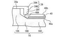
図4は、図3のベベルマスク39とその近傍の拡大図である。一例によれば、基板40は、デバイスが形成される面であるデバイス面40aと、デバイス面40aと反対側の面である裏面40bとを有する。基板40の外縁部分にある傾斜したところはベベル40Aである。デバイス面40aにはデバイスを形成するために周知の半導体プロセスが施され、その結果、基板40はある程度反っているかもしれない。 FIG. 4 is an enlarged view of the
図4の例では、サセプタ16は、外側から、上凸部分16A、中間部分16B、中央部分16Cを備えている。3つの部分のうち、上凸部分16Aの上面が最も高くなっている。中間部分16Bは上凸部分16Aから中央部分16Cにかけて高さが低くなるスロープとなっている。中央部分の上面は平坦な面となっている。 In the example of FIG. 4, the
図4の例では、ベベルマスク39は、本体部39Aと、本体部39Aの内縁側の下面にある凸部39Bを備えている。この例では、平坦面39aが上凸部分16Aに接した状態で、ベベルマスク39がサセプタ16の上にのせられている。さらに、傾斜面39bは、ベベル40Aに接触している。この例では、ベベルマスク39はベベル40Aだけに接し、裏面40bにもデバイス面40aにも接しない。傾斜面39bをベベル40Aに接触させることで、例えば反った基板40をサセプタ16に押し付けことができる。別の例によれば、傾斜面39bはベベル40Aに近接させるが接触させない。その場合、図4の傾斜面39bよりも若干上方に傾斜面を設ける。その結果、ベベルマスク39と基板40の接触はない。 In the example of FIG. 4, the
このように、基板40をサセプタ16の上にのせて、デバイス面40aとサセプタ16を対向させる。次いで、必要に応じてサセプタをプロセスポジションに移動させてから、裏面40bにプラズマ処理を施す。サセプタ16とシャワープレート14の間の空間へのガス供給と、シャワープレート14への高周波電力の印加を交互に行ったり、同時に行ったりする。この空間にプラズマを生じさせることで、裏面40bへの成膜、裏面40bへのエッチング処理、または裏面40bの膜の改質などを行う。一例によれば、このプラズマ処理は、裏面40bの全体に施される。しかし、ベベル40Aにはベベルマスク39が接触又は近接しているので、ベベル40Aへの有意なプラズマ処理はない。一例によれば、プラズマ処理によって裏面40bの全体へ成膜することによって、裏面に段差が生じることを回避できる。 In this way, the
上述の例では平行平板構造によってプラズマを生じさせるが、別の方法でプラズマを生じさせることができる。図1の例では、サセプタに対応して設けられるプラズマユニットとして、シャワープレート14が採用されている。しかし、そのようなプラズマユニットとして、周知のマイクロ波プラズマ生成装置を採用したり、周知の誘導結合プラズマ装置を採用したりすることができる。 In the above example, plasma is generated by the parallel plate structure, but plasma can be generated by another method. In the example of FIG. 1, the
図5は、別の例に係るベベルマスク39を示す断面図である。凸部39Bの下面の傾斜面は、平坦な傾斜面39bと、窪んだ曲面39cとを備えている。この曲面39cは、ベベル40Aに接触又は近接する面である。一例によれば、曲面39cによって、凸部39Bとベベル40Aの面接触が可能となったり、凸部39Bとベベル40Aの間隙を介したガスの侵入を抑制したりすることができる。 FIG. 5 is a cross-sectional view showing a
図6は、別の例に係るベベルマスク39を示す断面図である。凸部39Bの下面の傾斜面として、窪んだ曲面39dが提供されている。この例では、凸部39Bの下面の全体が曲面39dとなっている。そのため、基板40に位置ずれがあった場合においても曲面39dとベベル40Aを接触又は近接させることができる。
図5、6の曲面における曲率を、ベベル40Aの曲率の一致又は近い値とすることで、凸部39Bとベベル40Aの間隙を介したガスの侵入をさらに抑制することができる。FIG. 6 is a cross-sectional view showing a
By setting the curvature of the curved surface of FIGS. 5 and 6 to a value that matches or is close to the curvature of the
図7は、別の例に係るベベルマスク39を示す断面図である。凸部39Bの下面の傾斜面として、傾斜面39bと凸型の曲面39eとが設けられている。凸型の曲面39eは、ベベル40Aに接触又は近接する面である。 FIG. 7 is a cross-sectional view showing a
図8は、別の例に係るベベルマスク39を示す断面図である。凸部39Bの下面の傾斜面として、凸型の曲面39fを備えている。凸部38Bの下面の全体が凸型の曲面39fとなっている。
図7、8の例によれば、凸型の曲面39e、39fを設けることで、ベベルマスク39とベベル40Aを確実に接触させたり、十分近接させたりすることができる。FIG. 8 is a cross-sectional view showing a
According to the examples of FIGS. 7 and 8, by providing the convex
図9は、別の例に係る基板処理装置の断面図である。この基板処理装置は平行平板方式のプラズマ処理装置である。チャンバ12にはドア13が取り付けられ、チャンバ12の中に基板を提供したり、チャンバ12から基板を取り出したりすることができる。チャンバ12は、Dual Chamber Module(DCM) の一部、又はQuad Chamber Module (QCM)の一部として提供され得る。チャンバ12の中には上部カバー80が設けられている。一例によれば、上部カバー80はグランド電極として提供される。グランド電極とは接地用の電極である。 FIG. 9 is a cross-sectional view of the substrate processing apparatus according to another example. This substrate processing device is a parallel plate type plasma processing device. A
上部カバー80は、軸部分80aと、軸部分80aにつながっている円板部分80bを備えている。軸部分80aは、z正負方向に移動可能な第1昇降機構51に固定され、z正負方向に移動可能となっている。一例によれば、軸部分80aに固定された板51aがベローズ51bの上端に固定され、チャンバ12に固定された板51cをベローズ51bの下端に固定することで第1昇降機構51が提供される。第1昇降機構51として、上部カバー80をチャンバ12の内で上下動させる様々な構成を採用することができる。 The
円板部分80bは平面視で円形又は略円形となっている。上部カバー80の下面である円板部分80bの下面は、例えば、第1下面80cと、第1下面80cを囲み第1下面80cよりも下にある第2下面80dとを有している。そのため、円板部分80bの下面は中央に窪みを有する形状となっている。 The
接地電極である上部カバー80は平行平板構造において上部電極として機能する。容量結合プラズマを可能とし、放電を防止又は抑制するために、第1下面80cと第2下面80dの間の高さの差は例えば1mm以下とすることができる。 The
ベベルマスク90はチャンバ12の中に提供されている。ベベルマスク90は、平坦面90aとその平坦面90aによって囲まれた傾斜面90bを備えている。傾斜面90bは、上部カバー80との鉛直方向距離が上部カバー80の中央側で大きくなる面である。言いかえると、傾斜面90bは、水平方向と非平行であり、かつベベルマスク90で囲まれた部分の中央に向かって高さが低くなる面である。 The
一例によれば、ベベルマスク90は、支持棒91によって支持されている。支持棒91は、モータ52によって駆動する第2昇降機構53に固定されている。第2昇降機構53は支持棒91とベベルマスク90をチャンバ12の中で昇降させることができるように構成される。言いかえると、支持棒91とベベルマスク90は、モータ52と第2昇降機構53によって上又は下方向に移動可能となっている。一例によれば、第2昇降機構53は、支持棒91に固定されベローズ53bの上端に固定されたプレート53aと、チャンバ12に固定されベローズ53bの下端に固定されたプレート53cを備える。第2昇降機構53として、チャンバ12の中でベベルマスク90を上下動させる様々な構成を採用することができる。 According to one example, the
支持棒91とベベルマスク90は、例えば1つの絶縁体で一体形成され得る。ベベルマスク90は平面視で環状の形状を有している。ベベルマスク90は、環状の平坦面90aと、上部カバー80の直下にある傾斜面90bを備えている。一例によれば、図9に示されるように、平坦面90aの高さは傾斜面90bの高さ以上となっている。平坦面90aと傾斜面90bの高さの差は例えば処理対象となる基板40のアルミより大きい。別の例によれば、図10に示すように、平坦面90aの高さは傾斜面90bの高さより低い。 The support rod 91 and the
図10は、図9のベベルマスク90とその近傍の拡大図である。ベベルマスク90は、本体部90Aと、本体部の内縁側の上面にある凸部90Bと、を備えている。本体部90Aは平坦面90aを有し、凸部90Bは傾斜面90bを有している。傾斜面90bはベベルマスク90の中心側で本体部90Aとの鉛直方向距離が小さくなる斜面である。一例によれば、傾斜した第3下面80eがベベル40Aに接する。別の例によれば、第3下面80eが省略され、上部カバー80は基板40に接しない。 FIG. 10 is an enlarged view of the
傾斜面90bがベベル40Aに接することで、基板40がベベルマスク90によって支持されている。一例によれば、ベベルマスク90は、基板40のベベル40Aにだけ接し、基板40のベベル40A以外の部分には接しない。そのため、基板40の裏面40bが露出し、裏面40b全体へのプラズマ処理が可能となる。上述した様々な形状の傾斜面を、この傾斜面90bとして採用することができる。 The
図9には、チャンバ12の内壁近傍にある回転アーム92が図示されている。回転アーム92は例えばQCMを構成する4つのチャンバの中に基板を搬送するために設けられている。基板処理装置は、プラズマユニットを有し、そのプラズマユニットは上部カバー80とベベルマスク90の下の領域にプラズマを生じさせるように構成されている。図9の例では、プラズマユニットはシャワープレート93、ガス源94、95、及びRF電源96を備えている。シャワープレート93は上部カバー80の下に設けられ、上部カバー80に対向する。シャワープレート93は、スリットを有しガス源94、95からz正方向にガスを提供できるプレート93a、93cを有し、プレート93a、93c間に設けられたスペーサ93bを備えている。シャワープレート93の全体は金属で形成し得る。別の例によれば、少なくともプレート93cは金属で形成する。ガス源94、95はプラズマ処理に必要なガスを提供する。RF電源96はシャワープレート93に高周波電力を印加し、ガスをプラズマ状態にする。このように、上部カバー80とシャワープレート93を備えた平行平板構造を有する基板処理装置で、プラズマ処理が可能となっている。 FIG. 9 shows a
一例によれば、上部カバー80は、例えばモータ50で第1昇降機構51を動かすことで、上方に退避する。さらに、ベベルマスク90は、例えばモータ52によって第2昇降機構53を動かすことで、上方に退避する。その後、回転アーム92の一部である支持ピンを回転アーム92で回転させることで、支持ピンをチャンバ12内の基板受取位置に移行させる。基板支持のための支持ピンは回転アーム92を回転させることで4つのチャンバのいずれか1つに提供される。支持ピンはベベルマスク90によって囲まれた位置に設けられることができる。そして、ベベルマスク90が下方に移動し、支持ピンの上端より下まで達すると、上部カバー80の直下に設けられた支持ピンに基板が乗せられる。その後、ベベルマスク90を上方に移動させることで、傾斜面90bがベベル40Aに接する。この接触の結果、支持ピンは、基板40から離れ、回転アーム92の回転によって上部カバー80の直下の位置から退避させられる。その後、平坦面90aを上部カバー80に密着させつつ、上部カバー80と基板40の接触は回避する。 According to one example, the
この例では、上部カバー80を下方向に動かすことで、平坦面90aを第2下面80dに密着させた。一例によれば、第2下面80dの上に第1下面80cを設けることで、上部カバー80と基板40の接触を防止し得る。平坦面90aは第2下面80dの直下に位置しているので、第2下面80dが平坦面90aに接するとき、上部カバー80とベベルマスク90の間の空間をとおるガスの流れが抑制される。別の例によれば、上部カバー80の円板部分80bの下面が平坦である場合、上部カバーの下面が平坦面90aに接した結果、上部カバー80の下面と平坦面90aの間をとおるガスの流れが抑制される。 In this example, the
一例によれば、基板40、ベベルマスク90及び上部カバー80によって囲まれた空間が密閉空間となる。この場合、ガス源94、95から提供されたガスと平行平板間のプラズマは、その密閉空間に実質的に提供されない。そして、基板40の裏面40bにプラズマ処理が施される。一例によれば、基板40と上部カバー80の接触を回避することで、デバイス面40aを保護することができる。このような接触の回避は、上部カバー80の下面に凹部を設けることで確実にすることができる。一例によれば、基板40の裏面40bにプラズマ処理で形成された膜は基板40の反りを軽減する。 According to one example, the space surrounded by the
上記のいくつかの例では、サセプタ又は上部カバーである遮蔽部品と、基板のデバイス面が対向する。遮蔽部品がサセプタの場合は、サセプタ16と基板40が接触し、基板40のベベル40Aとベベルマスク39の接触は必須ではない。他方、遮蔽部品が上部カバー80の場合は、ベベルマスク90と基板40のベベル40Aが接触し、基板40と上部カバー80の接触は必須ではない。 In some of the above examples, the shield component, which is the susceptor or top cover, faces the device surface of the substrate. When the shielding component is a susceptor, the
上記の各例で説明したベベルマスクの傾斜面は、底面視で円形としてもよいし、ノッチ又はオリフラを考慮した形状としてもよい。具体的には、ノッチ又はオリフラと、ベベルマスクの傾斜面を接触または近接させることができるように、ベベルマスクの傾斜面を調整することができる。 The inclined surface of the bevel mask described in each of the above examples may be circular in terms of bottom view, or may have a shape in consideration of a notch or an orientation flat. Specifically, the inclined surface of the bevel mask can be adjusted so that the notch or the tilting surface can be brought into contact with or close to the inclined surface of the bevel mask.
12 チャンバ、 14 シャワープレート、 16 サセプタ、 39 ベベルマスク 12 chambers, 14 shower plates, 16 susceptors, 39 bevel masks
Claims (16)
Translated fromJapanese前記チャンバの中に設けられたサセプタ又は上部カバーである遮蔽部品と、
前記チャンバの中に設けられ、前記遮蔽部品との鉛直方向距離が前記遮蔽部品の中央側で大きくなる傾斜面を有するベベルマスクと、を備えた基板処理装置。With the chamber
A shielding component that is a susceptor or top cover provided in the chamber,
A substrate processing apparatus including a bevel mask provided in the chamber and having an inclined surface in which a vertical distance from the shielding component increases on the central side of the shielding component.
前記本体部の内縁側の下面又は上面にある凸部と、を備え、
前記凸部は中心側で前記本体部との距離が小さくなる傾斜面を有することを特徴とする、ベベルマスク。The main body with an annular shape and
A convex portion on the lower surface or the upper surface on the inner edge side of the main body portion is provided.
A bevel mask characterized in that the convex portion has an inclined surface on the center side where the distance from the main body portion is small.
べベルマスクの傾斜面を前記基板のべベルに接触又は近接させることと、
前記裏面にプラズマ処理を施すこと、とを備えた基板処理方法。The device surface of the substrate having the device surface, which is the surface on which the device is formed, and the back surface, which is the surface opposite to the device surface, is made to face the susceptor or the shielding component which is the upper cover.
Bringing the inclined surface of the bevel mask into contact with or close to the bevel of the substrate
A substrate processing method comprising applying plasma treatment to the back surface.
Applications Claiming Priority (2)
| Application Number | Priority Date | Filing Date | Title |
|---|---|---|---|
| US201962945061P | 2019-12-06 | 2019-12-06 | |
| US62/945,061 | 2019-12-06 |
Publications (1)
| Publication Number | Publication Date |
|---|---|
| JP2021091968Atrue JP2021091968A (en) | 2021-06-17 |
Family
ID=76163628
Family Applications (1)
| Application Number | Title | Priority Date | Filing Date |
|---|---|---|---|
| JP2020198766APendingJP2021091968A (en) | 2019-12-06 | 2020-11-30 | Substrate processing apparatus, bevel mask and substrate processing method |
Country Status (4)
| Country | Link |
|---|---|
| US (1) | US20210175052A1 (en) |
| JP (1) | JP2021091968A (en) |
| KR (1) | KR20210072697A (en) |
| CN (1) | CN112928011A (en) |
Families Citing this family (227)
| Publication number | Priority date | Publication date | Assignee | Title |
|---|---|---|---|---|
| US20130023129A1 (en) | 2011-07-20 | 2013-01-24 | Asm America, Inc. | Pressure transmitter for a semiconductor processing environment |
| US20160376700A1 (en) | 2013-02-01 | 2016-12-29 | Asm Ip Holding B.V. | System for treatment of deposition reactor |
| US10941490B2 (en) | 2014-10-07 | 2021-03-09 | Asm Ip Holding B.V. | Multiple temperature range susceptor, assembly, reactor and system including the susceptor, and methods of using the same |
| US10276355B2 (en) | 2015-03-12 | 2019-04-30 | Asm Ip Holding B.V. | Multi-zone reactor, system including the reactor, and method of using the same |
| US11139308B2 (en) | 2015-12-29 | 2021-10-05 | Asm Ip Holding B.V. | Atomic layer deposition of III-V compounds to form V-NAND devices |
| US10529554B2 (en) | 2016-02-19 | 2020-01-07 | Asm Ip Holding B.V. | Method for forming silicon nitride film selectively on sidewalls or flat surfaces of trenches |
| US10343920B2 (en) | 2016-03-18 | 2019-07-09 | Asm Ip Holding B.V. | Aligned carbon nanotubes |
| US11453943B2 (en) | 2016-05-25 | 2022-09-27 | Asm Ip Holding B.V. | Method for forming carbon-containing silicon/metal oxide or nitride film by ALD using silicon precursor and hydrocarbon precursor |
| US10612137B2 (en) | 2016-07-08 | 2020-04-07 | Asm Ip Holdings B.V. | Organic reactants for atomic layer deposition |
| US9859151B1 (en) | 2016-07-08 | 2018-01-02 | Asm Ip Holding B.V. | Selective film deposition method to form air gaps |
| US9812320B1 (en) | 2016-07-28 | 2017-11-07 | Asm Ip Holding B.V. | Method and apparatus for filling a gap |
| US9887082B1 (en) | 2016-07-28 | 2018-02-06 | Asm Ip Holding B.V. | Method and apparatus for filling a gap |
| US11532757B2 (en) | 2016-10-27 | 2022-12-20 | Asm Ip Holding B.V. | Deposition of charge trapping layers |
| US10714350B2 (en) | 2016-11-01 | 2020-07-14 | ASM IP Holdings, B.V. | Methods for forming a transition metal niobium nitride film on a substrate by atomic layer deposition and related semiconductor device structures |
| KR102546317B1 (en) | 2016-11-15 | 2023-06-21 | 에이에스엠 아이피 홀딩 비.브이. | Gas supply unit and substrate processing apparatus including the same |
| US11581186B2 (en) | 2016-12-15 | 2023-02-14 | Asm Ip Holding B.V. | Sequential infiltration synthesis apparatus |
| US11447861B2 (en) | 2016-12-15 | 2022-09-20 | Asm Ip Holding B.V. | Sequential infiltration synthesis apparatus and a method of forming a patterned structure |
| US11390950B2 (en) | 2017-01-10 | 2022-07-19 | Asm Ip Holding B.V. | Reactor system and method to reduce residue buildup during a film deposition process |
| US10468261B2 (en) | 2017-02-15 | 2019-11-05 | Asm Ip Holding B.V. | Methods for forming a metallic film on a substrate by cyclical deposition and related semiconductor device structures |
| US10770286B2 (en) | 2017-05-08 | 2020-09-08 | Asm Ip Holdings B.V. | Methods for selectively forming a silicon nitride film on a substrate and related semiconductor device structures |
| US12040200B2 (en) | 2017-06-20 | 2024-07-16 | Asm Ip Holding B.V. | Semiconductor processing apparatus and methods for calibrating a semiconductor processing apparatus |
| US11306395B2 (en) | 2017-06-28 | 2022-04-19 | Asm Ip Holding B.V. | Methods for depositing a transition metal nitride film on a substrate by atomic layer deposition and related deposition apparatus |
| KR20190009245A (en) | 2017-07-18 | 2019-01-28 | 에이에스엠 아이피 홀딩 비.브이. | Methods for forming a semiconductor device structure and related semiconductor device structures |
| US11374112B2 (en) | 2017-07-19 | 2022-06-28 | Asm Ip Holding B.V. | Method for depositing a group IV semiconductor and related semiconductor device structures |
| US10590535B2 (en) | 2017-07-26 | 2020-03-17 | Asm Ip Holdings B.V. | Chemical treatment, deposition and/or infiltration apparatus and method for using the same |
| TWI815813B (en) | 2017-08-04 | 2023-09-21 | 荷蘭商Asm智慧財產控股公司 | Showerhead assembly for distributing a gas within a reaction chamber |
| US10770336B2 (en) | 2017-08-08 | 2020-09-08 | Asm Ip Holding B.V. | Substrate lift mechanism and reactor including same |
| US10692741B2 (en) | 2017-08-08 | 2020-06-23 | Asm Ip Holdings B.V. | Radiation shield |
| US11769682B2 (en) | 2017-08-09 | 2023-09-26 | Asm Ip Holding B.V. | Storage apparatus for storing cassettes for substrates and processing apparatus equipped therewith |
| US11830730B2 (en) | 2017-08-29 | 2023-11-28 | Asm Ip Holding B.V. | Layer forming method and apparatus |
| US11295980B2 (en) | 2017-08-30 | 2022-04-05 | Asm Ip Holding B.V. | Methods for depositing a molybdenum metal film over a dielectric surface of a substrate by a cyclical deposition process and related semiconductor device structures |
| US10658205B2 (en) | 2017-09-28 | 2020-05-19 | Asm Ip Holdings B.V. | Chemical dispensing apparatus and methods for dispensing a chemical to a reaction chamber |
| US10403504B2 (en) | 2017-10-05 | 2019-09-03 | Asm Ip Holding B.V. | Method for selectively depositing a metallic film on a substrate |
| US10923344B2 (en) | 2017-10-30 | 2021-02-16 | Asm Ip Holding B.V. | Methods for forming a semiconductor structure and related semiconductor structures |
| CN111344522B (en) | 2017-11-27 | 2022-04-12 | 阿斯莫Ip控股公司 | Including clean mini-environment device |
| WO2019103613A1 (en) | 2017-11-27 | 2019-05-31 | Asm Ip Holding B.V. | A storage device for storing wafer cassettes for use with a batch furnace |
| US10872771B2 (en) | 2018-01-16 | 2020-12-22 | Asm Ip Holding B. V. | Method for depositing a material film on a substrate within a reaction chamber by a cyclical deposition process and related device structures |
| KR102695659B1 (en) | 2018-01-19 | 2024-08-14 | 에이에스엠 아이피 홀딩 비.브이. | Method for depositing a gap filling layer by plasma assisted deposition |
| TWI799494B (en) | 2018-01-19 | 2023-04-21 | 荷蘭商Asm 智慧財產控股公司 | Deposition method |
| US11081345B2 (en) | 2018-02-06 | 2021-08-03 | Asm Ip Holding B.V. | Method of post-deposition treatment for silicon oxide film |
| US10896820B2 (en) | 2018-02-14 | 2021-01-19 | Asm Ip Holding B.V. | Method for depositing a ruthenium-containing film on a substrate by a cyclical deposition process |
| WO2019158960A1 (en) | 2018-02-14 | 2019-08-22 | Asm Ip Holding B.V. | A method for depositing a ruthenium-containing film on a substrate by a cyclical deposition process |
| US10731249B2 (en) | 2018-02-15 | 2020-08-04 | Asm Ip Holding B.V. | Method of forming a transition metal containing film on a substrate by a cyclical deposition process, a method for supplying a transition metal halide compound to a reaction chamber, and related vapor deposition apparatus |
| KR102636427B1 (en) | 2018-02-20 | 2024-02-13 | 에이에스엠 아이피 홀딩 비.브이. | Substrate processing method and apparatus |
| US10975470B2 (en) | 2018-02-23 | 2021-04-13 | Asm Ip Holding B.V. | Apparatus for detecting or monitoring for a chemical precursor in a high temperature environment |
| US11473195B2 (en) | 2018-03-01 | 2022-10-18 | Asm Ip Holding B.V. | Semiconductor processing apparatus and a method for processing a substrate |
| KR102646467B1 (en) | 2018-03-27 | 2024-03-11 | 에이에스엠 아이피 홀딩 비.브이. | Method of forming an electrode on a substrate and a semiconductor device structure including an electrode |
| KR102600229B1 (en) | 2018-04-09 | 2023-11-10 | 에이에스엠 아이피 홀딩 비.브이. | Substrate supporting device, substrate processing apparatus including the same and substrate processing method |
| US12025484B2 (en) | 2018-05-08 | 2024-07-02 | Asm Ip Holding B.V. | Thin film forming method |
| US12272527B2 (en) | 2018-05-09 | 2025-04-08 | Asm Ip Holding B.V. | Apparatus for use with hydrogen radicals and method of using same |
| KR102596988B1 (en) | 2018-05-28 | 2023-10-31 | 에이에스엠 아이피 홀딩 비.브이. | Method of processing a substrate and a device manufactured by the same |
| US11718913B2 (en) | 2018-06-04 | 2023-08-08 | Asm Ip Holding B.V. | Gas distribution system and reactor system including same |
| US10797133B2 (en) | 2018-06-21 | 2020-10-06 | Asm Ip Holding B.V. | Method for depositing a phosphorus doped silicon arsenide film and related semiconductor device structures |
| KR102568797B1 (en) | 2018-06-21 | 2023-08-21 | 에이에스엠 아이피 홀딩 비.브이. | Substrate processing system |
| KR102854019B1 (en) | 2018-06-27 | 2025-09-02 | 에이에스엠 아이피 홀딩 비.브이. | Periodic deposition method for forming a metal-containing material and films and structures comprising the metal-containing material |
| TWI873894B (en) | 2018-06-27 | 2025-02-21 | 荷蘭商Asm Ip私人控股有限公司 | Cyclic deposition methods for forming metal-containing material and films and structures including the metal-containing material |
| US10388513B1 (en) | 2018-07-03 | 2019-08-20 | Asm Ip Holding B.V. | Method for depositing silicon-free carbon-containing film as gap-fill layer by pulse plasma-assisted deposition |
| US10755922B2 (en) | 2018-07-03 | 2020-08-25 | Asm Ip Holding B.V. | Method for depositing silicon-free carbon-containing film as gap-fill layer by pulse plasma-assisted deposition |
| US11430674B2 (en) | 2018-08-22 | 2022-08-30 | Asm Ip Holding B.V. | Sensor array, apparatus for dispensing a vapor phase reactant to a reaction chamber and related methods |
| KR102707956B1 (en) | 2018-09-11 | 2024-09-19 | 에이에스엠 아이피 홀딩 비.브이. | Method for deposition of a thin film |
| US11024523B2 (en) | 2018-09-11 | 2021-06-01 | Asm Ip Holding B.V. | Substrate processing apparatus and method |
| CN110970344B (en) | 2018-10-01 | 2024-10-25 | Asmip控股有限公司 | Substrate holding apparatus, system comprising the same and method of using the same |
| KR102592699B1 (en) | 2018-10-08 | 2023-10-23 | 에이에스엠 아이피 홀딩 비.브이. | Substrate support unit and apparatuses for depositing thin film and processing the substrate including the same |
| KR102546322B1 (en) | 2018-10-19 | 2023-06-21 | 에이에스엠 아이피 홀딩 비.브이. | Substrate processing apparatus and substrate processing method |
| US12378665B2 (en) | 2018-10-26 | 2025-08-05 | Asm Ip Holding B.V. | High temperature coatings for a preclean and etch apparatus and related methods |
| US11087997B2 (en) | 2018-10-31 | 2021-08-10 | Asm Ip Holding B.V. | Substrate processing apparatus for processing substrates |
| KR102748291B1 (en) | 2018-11-02 | 2024-12-31 | 에이에스엠 아이피 홀딩 비.브이. | Substrate support unit and substrate processing apparatus including the same |
| US11572620B2 (en) | 2018-11-06 | 2023-02-07 | Asm Ip Holding B.V. | Methods for selectively depositing an amorphous silicon film on a substrate |
| US10818758B2 (en) | 2018-11-16 | 2020-10-27 | Asm Ip Holding B.V. | Methods for forming a metal silicate film on a substrate in a reaction chamber and related semiconductor device structures |
| US12040199B2 (en) | 2018-11-28 | 2024-07-16 | Asm Ip Holding B.V. | Substrate processing apparatus for processing substrates |
| KR102636428B1 (en) | 2018-12-04 | 2024-02-13 | 에이에스엠 아이피 홀딩 비.브이. | A method for cleaning a substrate processing apparatus |
| US11158513B2 (en) | 2018-12-13 | 2021-10-26 | Asm Ip Holding B.V. | Methods for forming a rhenium-containing film on a substrate by a cyclical deposition process and related semiconductor device structures |
| TWI874340B (en) | 2018-12-14 | 2025-03-01 | 荷蘭商Asm Ip私人控股有限公司 | Method of forming device structure, structure formed by the method and system for performing the method |
| TWI866480B (en) | 2019-01-17 | 2024-12-11 | 荷蘭商Asm Ip 私人控股有限公司 | Methods of forming a transition metal containing film on a substrate by a cyclical deposition process |
| TWI838458B (en) | 2019-02-20 | 2024-04-11 | 荷蘭商Asm Ip私人控股有限公司 | Apparatus and methods for plug fill deposition in 3-d nand applications |
| TWI873122B (en) | 2019-02-20 | 2025-02-21 | 荷蘭商Asm Ip私人控股有限公司 | Method of filling a recess formed within a surface of a substrate, semiconductor structure formed according to the method, and semiconductor processing apparatus |
| TWI845607B (en) | 2019-02-20 | 2024-06-21 | 荷蘭商Asm Ip私人控股有限公司 | Cyclical deposition method and apparatus for filling a recess formed within a substrate surface |
| TWI842826B (en) | 2019-02-22 | 2024-05-21 | 荷蘭商Asm Ip私人控股有限公司 | Substrate processing apparatus and method for processing substrate |
| KR102858005B1 (en) | 2019-03-08 | 2025-09-09 | 에이에스엠 아이피 홀딩 비.브이. | Method for Selective Deposition of Silicon Nitride Layer and Structure Including Selectively-Deposited Silicon Nitride Layer |
| US11742198B2 (en) | 2019-03-08 | 2023-08-29 | Asm Ip Holding B.V. | Structure including SiOCN layer and method of forming same |
| JP2020167398A (en) | 2019-03-28 | 2020-10-08 | エーエスエム・アイピー・ホールディング・ベー・フェー | Door openers and substrate processing equipment provided with door openers |
| KR102809999B1 (en) | 2019-04-01 | 2025-05-19 | 에이에스엠 아이피 홀딩 비.브이. | Method of manufacturing semiconductor device |
| KR20200123380A (en) | 2019-04-19 | 2020-10-29 | 에이에스엠 아이피 홀딩 비.브이. | Layer forming method and apparatus |
| KR20200125453A (en) | 2019-04-24 | 2020-11-04 | 에이에스엠 아이피 홀딩 비.브이. | Gas-phase reactor system and method of using same |
| KR20200130121A (en) | 2019-05-07 | 2020-11-18 | 에이에스엠 아이피 홀딩 비.브이. | Chemical source vessel with dip tube |
| KR20200130652A (en) | 2019-05-10 | 2020-11-19 | 에이에스엠 아이피 홀딩 비.브이. | Method of depositing material onto a surface and structure formed according to the method |
| JP7612342B2 (en) | 2019-05-16 | 2025-01-14 | エーエスエム・アイピー・ホールディング・ベー・フェー | Wafer boat handling apparatus, vertical batch furnace and method |
| JP7598201B2 (en) | 2019-05-16 | 2024-12-11 | エーエスエム・アイピー・ホールディング・ベー・フェー | Wafer boat handling apparatus, vertical batch furnace and method |
| USD975665S1 (en) | 2019-05-17 | 2023-01-17 | Asm Ip Holding B.V. | Susceptor shaft |
| USD947913S1 (en) | 2019-05-17 | 2022-04-05 | Asm Ip Holding B.V. | Susceptor shaft |
| KR20200141002A (en) | 2019-06-06 | 2020-12-17 | 에이에스엠 아이피 홀딩 비.브이. | Method of using a gas-phase reactor system including analyzing exhausted gas |
| KR20200141931A (en) | 2019-06-10 | 2020-12-21 | 에이에스엠 아이피 홀딩 비.브이. | Method for cleaning quartz epitaxial chambers |
| KR20200143254A (en) | 2019-06-11 | 2020-12-23 | 에이에스엠 아이피 홀딩 비.브이. | Method of forming an electronic structure using an reforming gas, system for performing the method, and structure formed using the method |
| KR20210005515A (en) | 2019-07-03 | 2021-01-14 | 에이에스엠 아이피 홀딩 비.브이. | Temperature control assembly for substrate processing apparatus and method of using same |
| JP7499079B2 (en) | 2019-07-09 | 2024-06-13 | エーエスエム・アイピー・ホールディング・ベー・フェー | Plasma device using coaxial waveguide and substrate processing method |
| CN112216646A (en) | 2019-07-10 | 2021-01-12 | Asm Ip私人控股有限公司 | Substrate supporting assembly and substrate processing device comprising same |
| KR20210010307A (en) | 2019-07-16 | 2021-01-27 | 에이에스엠 아이피 홀딩 비.브이. | Substrate processing apparatus |
| KR102860110B1 (en) | 2019-07-17 | 2025-09-16 | 에이에스엠 아이피 홀딩 비.브이. | Methods of forming silicon germanium structures |
| KR20210010816A (en) | 2019-07-17 | 2021-01-28 | 에이에스엠 아이피 홀딩 비.브이. | Radical assist ignition plasma system and method |
| US11643724B2 (en) | 2019-07-18 | 2023-05-09 | Asm Ip Holding B.V. | Method of forming structures using a neutral beam |
| KR20210010817A (en) | 2019-07-19 | 2021-01-28 | 에이에스엠 아이피 홀딩 비.브이. | Method of Forming Topology-Controlled Amorphous Carbon Polymer Film |
| TWI851767B (en) | 2019-07-29 | 2024-08-11 | 荷蘭商Asm Ip私人控股有限公司 | Methods for selective deposition utilizing n-type dopants and/or alternative dopants to achieve high dopant incorporation |
| US12169361B2 (en) | 2019-07-30 | 2024-12-17 | Asm Ip Holding B.V. | Substrate processing apparatus and method |
| CN112309900A (en) | 2019-07-30 | 2021-02-02 | Asm Ip私人控股有限公司 | Substrate processing apparatus |
| CN112309899A (en) | 2019-07-30 | 2021-02-02 | Asm Ip私人控股有限公司 | Substrate processing apparatus |
| US11587815B2 (en) | 2019-07-31 | 2023-02-21 | Asm Ip Holding B.V. | Vertical batch furnace assembly |
| US11587814B2 (en) | 2019-07-31 | 2023-02-21 | Asm Ip Holding B.V. | Vertical batch furnace assembly |
| US11227782B2 (en) | 2019-07-31 | 2022-01-18 | Asm Ip Holding B.V. | Vertical batch furnace assembly |
| CN112323048B (en) | 2019-08-05 | 2024-02-09 | Asm Ip私人控股有限公司 | Liquid level sensor for chemical source container |
| CN112342526A (en) | 2019-08-09 | 2021-02-09 | Asm Ip私人控股有限公司 | Heater assembly including cooling device and method of using same |
| USD965044S1 (en) | 2019-08-19 | 2022-09-27 | Asm Ip Holding B.V. | Susceptor shaft |
| USD965524S1 (en) | 2019-08-19 | 2022-10-04 | Asm Ip Holding B.V. | Susceptor support |
| JP2021031769A (en) | 2019-08-21 | 2021-03-01 | エーエスエム アイピー ホールディング ビー.ブイ. | Production apparatus of mixed gas of film deposition raw material and film deposition apparatus |
| KR20210024423A (en) | 2019-08-22 | 2021-03-05 | 에이에스엠 아이피 홀딩 비.브이. | Method for forming a structure with a hole |
| USD979506S1 (en) | 2019-08-22 | 2023-02-28 | Asm Ip Holding B.V. | Insulator |
| US11286558B2 (en) | 2019-08-23 | 2022-03-29 | Asm Ip Holding B.V. | Methods for depositing a molybdenum nitride film on a surface of a substrate by a cyclical deposition process and related semiconductor device structures including a molybdenum nitride film |
| KR20210024420A (en) | 2019-08-23 | 2021-03-05 | 에이에스엠 아이피 홀딩 비.브이. | Method for depositing silicon oxide film having improved quality by peald using bis(diethylamino)silane |
| KR102806450B1 (en) | 2019-09-04 | 2025-05-12 | 에이에스엠 아이피 홀딩 비.브이. | Methods for selective deposition using a sacrificial capping layer |
| KR102733104B1 (en) | 2019-09-05 | 2024-11-22 | 에이에스엠 아이피 홀딩 비.브이. | Substrate processing apparatus |
| US11562901B2 (en) | 2019-09-25 | 2023-01-24 | Asm Ip Holding B.V. | Substrate processing method |
| CN112593212B (en) | 2019-10-02 | 2023-12-22 | Asm Ip私人控股有限公司 | Method for forming topologically selective silicon oxide film by cyclic plasma enhanced deposition process |
| KR20210042810A (en) | 2019-10-08 | 2021-04-20 | 에이에스엠 아이피 홀딩 비.브이. | Reactor system including a gas distribution assembly for use with activated species and method of using same |
| TW202128273A (en) | 2019-10-08 | 2021-08-01 | 荷蘭商Asm Ip私人控股有限公司 | Gas injection system, reactor system, and method of depositing material on surface of substratewithin reaction chamber |
| TWI846953B (en) | 2019-10-08 | 2024-07-01 | 荷蘭商Asm Ip私人控股有限公司 | Substrate processing device |
| TWI846966B (en) | 2019-10-10 | 2024-07-01 | 荷蘭商Asm Ip私人控股有限公司 | Method of forming a photoresist underlayer and structure including same |
| US12009241B2 (en) | 2019-10-14 | 2024-06-11 | Asm Ip Holding B.V. | Vertical batch furnace assembly with detector to detect cassette |
| TWI834919B (en) | 2019-10-16 | 2024-03-11 | 荷蘭商Asm Ip私人控股有限公司 | Method of topology-selective film formation of silicon oxide |
| US11637014B2 (en) | 2019-10-17 | 2023-04-25 | Asm Ip Holding B.V. | Methods for selective deposition of doped semiconductor material |
| KR102845724B1 (en) | 2019-10-21 | 2025-08-13 | 에이에스엠 아이피 홀딩 비.브이. | Apparatus and methods for selectively etching films |
| KR20210050453A (en) | 2019-10-25 | 2021-05-07 | 에이에스엠 아이피 홀딩 비.브이. | Methods for filling a gap feature on a substrate surface and related semiconductor structures |
| US11646205B2 (en) | 2019-10-29 | 2023-05-09 | Asm Ip Holding B.V. | Methods of selectively forming n-type doped material on a surface, systems for selectively forming n-type doped material, and structures formed using same |
| KR20210054983A (en) | 2019-11-05 | 2021-05-14 | 에이에스엠 아이피 홀딩 비.브이. | Structures with doped semiconductor layers and methods and systems for forming same |
| US11501968B2 (en) | 2019-11-15 | 2022-11-15 | Asm Ip Holding B.V. | Method for providing a semiconductor device with silicon filled gaps |
| KR102861314B1 (en) | 2019-11-20 | 2025-09-17 | 에이에스엠 아이피 홀딩 비.브이. | Method of depositing carbon-containing material on a surface of a substrate, structure formed using the method, and system for forming the structure |
| CN112951697B (en) | 2019-11-26 | 2025-07-29 | Asmip私人控股有限公司 | Substrate processing apparatus |
| US11450529B2 (en) | 2019-11-26 | 2022-09-20 | Asm Ip Holding B.V. | Methods for selectively forming a target film on a substrate comprising a first dielectric surface and a second metallic surface |
| CN120432376A (en) | 2019-11-29 | 2025-08-05 | Asm Ip私人控股有限公司 | Substrate processing apparatus |
| CN112885692B (en) | 2019-11-29 | 2025-08-15 | Asmip私人控股有限公司 | Substrate processing apparatus |
| JP7527928B2 (en) | 2019-12-02 | 2024-08-05 | エーエスエム・アイピー・ホールディング・ベー・フェー | Substrate processing apparatus and substrate processing method |
| KR20210070898A (en) | 2019-12-04 | 2021-06-15 | 에이에스엠 아이피 홀딩 비.브이. | Substrate processing apparatus |
| KR20210078405A (en) | 2019-12-17 | 2021-06-28 | 에이에스엠 아이피 홀딩 비.브이. | Method of forming vanadium nitride layer and structure including the vanadium nitride layer |
| KR20210080214A (en) | 2019-12-19 | 2021-06-30 | 에이에스엠 아이피 홀딩 비.브이. | Methods for filling a gap feature on a substrate and related semiconductor structures |
| JP7730637B2 (en) | 2020-01-06 | 2025-08-28 | エーエスエム・アイピー・ホールディング・ベー・フェー | Gas delivery assembly, components thereof, and reactor system including same |
| JP7636892B2 (en) | 2020-01-06 | 2025-02-27 | エーエスエム・アイピー・ホールディング・ベー・フェー | Channeled Lift Pins |
| US11993847B2 (en) | 2020-01-08 | 2024-05-28 | Asm Ip Holding B.V. | Injector |
| KR20210093163A (en) | 2020-01-16 | 2021-07-27 | 에이에스엠 아이피 홀딩 비.브이. | Method of forming high aspect ratio features |
| KR102675856B1 (en) | 2020-01-20 | 2024-06-17 | 에이에스엠 아이피 홀딩 비.브이. | Method of forming thin film and method of modifying surface of thin film |
| TWI889744B (en) | 2020-01-29 | 2025-07-11 | 荷蘭商Asm Ip私人控股有限公司 | Contaminant trap system, and baffle plate stack |
| TW202513845A (en) | 2020-02-03 | 2025-04-01 | 荷蘭商Asm Ip私人控股有限公司 | Semiconductor structures and methods for forming the same |
| KR20210100010A (en) | 2020-02-04 | 2021-08-13 | 에이에스엠 아이피 홀딩 비.브이. | Method and apparatus for transmittance measurements of large articles |
| US11776846B2 (en) | 2020-02-07 | 2023-10-03 | Asm Ip Holding B.V. | Methods for depositing gap filling fluids and related systems and devices |
| KR20210103956A (en) | 2020-02-13 | 2021-08-24 | 에이에스엠 아이피 홀딩 비.브이. | Substrate processing apparatus including light receiving device and calibration method of light receiving device |
| TW202146691A (en) | 2020-02-13 | 2021-12-16 | 荷蘭商Asm Ip私人控股有限公司 | Gas distribution assembly, shower plate assembly, and method of adjusting conductance of gas to reaction chamber |
| TWI855223B (en) | 2020-02-17 | 2024-09-11 | 荷蘭商Asm Ip私人控股有限公司 | Method for growing phosphorous-doped silicon layer |
| CN113410160A (en) | 2020-02-28 | 2021-09-17 | Asm Ip私人控股有限公司 | System specially used for cleaning parts |
| KR20210113043A (en) | 2020-03-04 | 2021-09-15 | 에이에스엠 아이피 홀딩 비.브이. | Alignment fixture for a reactor system |
| US11876356B2 (en) | 2020-03-11 | 2024-01-16 | Asm Ip Holding B.V. | Lockout tagout assembly and system and method of using same |
| KR20210116240A (en) | 2020-03-11 | 2021-09-27 | 에이에스엠 아이피 홀딩 비.브이. | Substrate handling device with adjustable joints |
| KR102775390B1 (en) | 2020-03-12 | 2025-02-28 | 에이에스엠 아이피 홀딩 비.브이. | Method for Fabricating Layer Structure Having Target Topological Profile |
| US12173404B2 (en) | 2020-03-17 | 2024-12-24 | Asm Ip Holding B.V. | Method of depositing epitaxial material, structure formed using the method, and system for performing the method |
| KR102755229B1 (en) | 2020-04-02 | 2025-01-14 | 에이에스엠 아이피 홀딩 비.브이. | Thin film forming method |
| TWI887376B (en) | 2020-04-03 | 2025-06-21 | 荷蘭商Asm Ip私人控股有限公司 | Method for manufacturing semiconductor device |
| TWI888525B (en) | 2020-04-08 | 2025-07-01 | 荷蘭商Asm Ip私人控股有限公司 | Apparatus and methods for selectively etching silcon oxide films |
| KR20210127620A (en) | 2020-04-13 | 2021-10-22 | 에이에스엠 아이피 홀딩 비.브이. | method of forming a nitrogen-containing carbon film and system for performing the method |
| US11821078B2 (en) | 2020-04-15 | 2023-11-21 | Asm Ip Holding B.V. | Method for forming precoat film and method for forming silicon-containing film |
| KR20210128343A (en) | 2020-04-15 | 2021-10-26 | 에이에스엠 아이피 홀딩 비.브이. | Method of forming chromium nitride layer and structure including the chromium nitride layer |
| US11996289B2 (en) | 2020-04-16 | 2024-05-28 | Asm Ip Holding B.V. | Methods of forming structures including silicon germanium and silicon layers, devices formed using the methods, and systems for performing the methods |
| KR20210130646A (en) | 2020-04-21 | 2021-11-01 | 에이에스엠 아이피 홀딩 비.브이. | Method for processing a substrate |
| KR20210132612A (en) | 2020-04-24 | 2021-11-04 | 에이에스엠 아이피 홀딩 비.브이. | Methods and apparatus for stabilizing vanadium compounds |
| KR20210132600A (en) | 2020-04-24 | 2021-11-04 | 에이에스엠 아이피 홀딩 비.브이. | Methods and systems for depositing a layer comprising vanadium, nitrogen, and a further element |
| KR102866804B1 (en) | 2020-04-24 | 2025-09-30 | 에이에스엠 아이피 홀딩 비.브이. | Vertical batch furnace assembly comprising a cooling gas supply |
| CN113555279A (en) | 2020-04-24 | 2021-10-26 | Asm Ip私人控股有限公司 | Methods of forming vanadium nitride-containing layers and structures comprising the same |
| TW202208671A (en) | 2020-04-24 | 2022-03-01 | 荷蘭商Asm Ip私人控股有限公司 | Methods of forming structures including vanadium boride and vanadium phosphide layers |
| KR102783898B1 (en) | 2020-04-29 | 2025-03-18 | 에이에스엠 아이피 홀딩 비.브이. | Solid source precursor vessel |
| KR20210134869A (en) | 2020-05-01 | 2021-11-11 | 에이에스엠 아이피 홀딩 비.브이. | Fast FOUP swapping with a FOUP handler |
| JP7726664B2 (en) | 2020-05-04 | 2025-08-20 | エーエスエム・アイピー・ホールディング・ベー・フェー | Substrate processing system for processing a substrate |
| KR20210137395A (en) | 2020-05-07 | 2021-11-17 | 에이에스엠 아이피 홀딩 비.브이. | Apparatus and methods for performing an in-situ etch of reaction chambers with fluorine-based radicals |
| KR102788543B1 (en) | 2020-05-13 | 2025-03-27 | 에이에스엠 아이피 홀딩 비.브이. | Laser alignment fixture for a reactor system |
| TW202146699A (en) | 2020-05-15 | 2021-12-16 | 荷蘭商Asm Ip私人控股有限公司 | Method of forming a silicon germanium layer, semiconductor structure, semiconductor device, method of forming a deposition layer, and deposition system |
| KR20210143653A (en) | 2020-05-19 | 2021-11-29 | 에이에스엠 아이피 홀딩 비.브이. | Substrate processing apparatus |
| KR102795476B1 (en) | 2020-05-21 | 2025-04-11 | 에이에스엠 아이피 홀딩 비.브이. | Structures including multiple carbon layers and methods of forming and using same |
| KR20210145079A (en) | 2020-05-21 | 2021-12-01 | 에이에스엠 아이피 홀딩 비.브이. | Flange and apparatus for processing substrates |
| TWI873343B (en) | 2020-05-22 | 2025-02-21 | 荷蘭商Asm Ip私人控股有限公司 | Reaction system for forming thin film on substrate |
| KR20210146802A (en) | 2020-05-26 | 2021-12-06 | 에이에스엠 아이피 홀딩 비.브이. | Method for depositing boron and gallium containing silicon germanium layers |
| TWI876048B (en) | 2020-05-29 | 2025-03-11 | 荷蘭商Asm Ip私人控股有限公司 | Substrate processing device |
| TW202212620A (en) | 2020-06-02 | 2022-04-01 | 荷蘭商Asm Ip私人控股有限公司 | Apparatus for processing substrate, method of forming film, and method of controlling apparatus for processing substrate |
| TW202208659A (en) | 2020-06-16 | 2022-03-01 | 荷蘭商Asm Ip私人控股有限公司 | Method for depositing boron containing silicon germanium layers |
| TW202218133A (en) | 2020-06-24 | 2022-05-01 | 荷蘭商Asm Ip私人控股有限公司 | Method for forming a layer provided with silicon |
| TWI873359B (en) | 2020-06-30 | 2025-02-21 | 荷蘭商Asm Ip私人控股有限公司 | Substrate processing method |
| TW202202649A (en) | 2020-07-08 | 2022-01-16 | 荷蘭商Asm Ip私人控股有限公司 | Substrate processing method |
| KR20220010438A (en) | 2020-07-17 | 2022-01-25 | 에이에스엠 아이피 홀딩 비.브이. | Structures and methods for use in photolithography |
| KR20220011092A (en) | 2020-07-20 | 2022-01-27 | 에이에스엠 아이피 홀딩 비.브이. | Method and system for forming structures including transition metal layers |
| TWI878570B (en) | 2020-07-20 | 2025-04-01 | 荷蘭商Asm Ip私人控股有限公司 | Method and system for depositing molybdenum layers |
| US12322591B2 (en) | 2020-07-27 | 2025-06-03 | Asm Ip Holding B.V. | Thin film deposition process |
| KR20220021863A (en) | 2020-08-14 | 2022-02-22 | 에이에스엠 아이피 홀딩 비.브이. | Method for processing a substrate |
| US12040177B2 (en) | 2020-08-18 | 2024-07-16 | Asm Ip Holding B.V. | Methods for forming a laminate film by cyclical plasma-enhanced deposition processes |
| TW202228863A (en) | 2020-08-25 | 2022-08-01 | 荷蘭商Asm Ip私人控股有限公司 | Method for cleaning a substrate, method for selectively depositing, and reaction system |
| US11725280B2 (en) | 2020-08-26 | 2023-08-15 | Asm Ip Holding B.V. | Method for forming metal silicon oxide and metal silicon oxynitride layers |
| TW202229601A (en) | 2020-08-27 | 2022-08-01 | 荷蘭商Asm Ip私人控股有限公司 | Method of forming patterned structures, method of manipulating mechanical property, device structure, and substrate processing system |
| USD990534S1 (en) | 2020-09-11 | 2023-06-27 | Asm Ip Holding B.V. | Weighted lift pin |
| KR20220036866A (en) | 2020-09-16 | 2022-03-23 | 에이에스엠 아이피 홀딩 비.브이. | Silicon oxide deposition method |
| USD1012873S1 (en) | 2020-09-24 | 2024-01-30 | Asm Ip Holding B.V. | Electrode for semiconductor processing apparatus |
| TWI889903B (en) | 2020-09-25 | 2025-07-11 | 荷蘭商Asm Ip私人控股有限公司 | Semiconductor processing method |
| US12009224B2 (en) | 2020-09-29 | 2024-06-11 | Asm Ip Holding B.V. | Apparatus and method for etching metal nitrides |
| KR20220045900A (en) | 2020-10-06 | 2022-04-13 | 에이에스엠 아이피 홀딩 비.브이. | Deposition method and an apparatus for depositing a silicon-containing material |
| CN114293174A (en) | 2020-10-07 | 2022-04-08 | Asm Ip私人控股有限公司 | Gas supply unit and substrate processing apparatus including the same |
| TW202229613A (en) | 2020-10-14 | 2022-08-01 | 荷蘭商Asm Ip私人控股有限公司 | Method of depositing material on stepped structure |
| TW202232565A (en) | 2020-10-15 | 2022-08-16 | 荷蘭商Asm Ip私人控股有限公司 | Method of manufacturing semiconductor device, and substrate treatment apparatus using ether-cat |
| TW202217037A (en) | 2020-10-22 | 2022-05-01 | 荷蘭商Asm Ip私人控股有限公司 | Method of depositing vanadium metal, structure, device and a deposition assembly |
| TW202223136A (en) | 2020-10-28 | 2022-06-16 | 荷蘭商Asm Ip私人控股有限公司 | Method for forming layer on substrate, and semiconductor processing system |
| TW202229620A (en) | 2020-11-12 | 2022-08-01 | 特文特大學 | Deposition system, method for controlling reaction condition, method for depositing |
| TW202229795A (en) | 2020-11-23 | 2022-08-01 | 荷蘭商Asm Ip私人控股有限公司 | A substrate processing apparatus with an injector |
| TW202235649A (en) | 2020-11-24 | 2022-09-16 | 荷蘭商Asm Ip私人控股有限公司 | Methods for filling a gap and related systems and devices |
| TW202235675A (en) | 2020-11-30 | 2022-09-16 | 荷蘭商Asm Ip私人控股有限公司 | Injector, and substrate processing apparatus |
| US12255053B2 (en) | 2020-12-10 | 2025-03-18 | Asm Ip Holding B.V. | Methods and systems for depositing a layer |
| TW202233884A (en) | 2020-12-14 | 2022-09-01 | 荷蘭商Asm Ip私人控股有限公司 | Method of forming structures for threshold voltage control |
| US11946137B2 (en) | 2020-12-16 | 2024-04-02 | Asm Ip Holding B.V. | Runout and wobble measurement fixtures |
| TW202232639A (en) | 2020-12-18 | 2022-08-16 | 荷蘭商Asm Ip私人控股有限公司 | Wafer processing apparatus with a rotatable table |
| TW202226899A (en) | 2020-12-22 | 2022-07-01 | 荷蘭商Asm Ip私人控股有限公司 | Plasma treatment device having matching box |
| TW202231903A (en) | 2020-12-22 | 2022-08-16 | 荷蘭商Asm Ip私人控股有限公司 | Transition metal deposition method, transition metal layer, and deposition assembly for depositing transition metal on substrate |
| TW202242184A (en) | 2020-12-22 | 2022-11-01 | 荷蘭商Asm Ip私人控股有限公司 | Precursor capsule, precursor vessel, vapor deposition assembly, and method of loading solid precursor into precursor vessel |
| USD1023959S1 (en) | 2021-05-11 | 2024-04-23 | Asm Ip Holding B.V. | Electrode for substrate processing apparatus |
| USD980814S1 (en) | 2021-05-11 | 2023-03-14 | Asm Ip Holding B.V. | Gas distributor for substrate processing apparatus |
| USD980813S1 (en) | 2021-05-11 | 2023-03-14 | Asm Ip Holding B.V. | Gas flow control plate for substrate processing apparatus |
| USD981973S1 (en) | 2021-05-11 | 2023-03-28 | Asm Ip Holding B.V. | Reactor wall for substrate processing apparatus |
| USD990441S1 (en) | 2021-09-07 | 2023-06-27 | Asm Ip Holding B.V. | Gas flow control plate |
| USD1060598S1 (en) | 2021-12-03 | 2025-02-04 | Asm Ip Holding B.V. | Split showerhead cover |
Citations (4)
| Publication number | Priority date | Publication date | Assignee | Title |
|---|---|---|---|---|
| JP2001073135A (en)* | 1999-06-04 | 2001-03-21 | Applied Materials Inc | Equipment for processing substrates |
| JP2002009136A (en)* | 2000-03-16 | 2002-01-11 | Applied Materials Inc | Shadow ring with common guide member |
| JP2014098202A (en)* | 2012-11-15 | 2014-05-29 | Tokyo Electron Ltd | Film deposition apparatus |
| US9881788B2 (en)* | 2014-05-22 | 2018-01-30 | Lam Research Corporation | Back side deposition apparatus and applications |
Family Cites Families (5)
| Publication number | Priority date | Publication date | Assignee | Title |
|---|---|---|---|---|
| JP4288767B2 (en)* | 1999-07-07 | 2009-07-01 | 東京エレクトロン株式会社 | Manufacturing method of semiconductor device |
| TWI224815B (en)* | 2001-08-01 | 2004-12-01 | Tokyo Electron Ltd | Gas processing apparatus and gas processing method |
| JP2005120410A (en)* | 2003-10-15 | 2005-05-12 | Renesas Technology Corp | Method of fabricating semiconductor device |
| JP4841873B2 (en)* | 2005-06-23 | 2011-12-21 | 大日本スクリーン製造株式会社 | Heat treatment susceptor and heat treatment apparatus |
| KR102124441B1 (en)* | 2009-12-31 | 2020-06-18 | 어플라이드 머티어리얼스, 인코포레이티드 | Shadow ring for modifying wafer edge and bevel deposition |
- 2020
- 2020-11-30JPJP2020198766Apatent/JP2021091968A/enactivePending
- 2020-11-30KRKR1020200164216Apatent/KR20210072697A/enactivePending
- 2020-12-01USUS17/109,080patent/US20210175052A1/enactivePending
- 2020-12-04CNCN202011412382.0Apatent/CN112928011A/enactivePending
Patent Citations (4)
| Publication number | Priority date | Publication date | Assignee | Title |
|---|---|---|---|---|
| JP2001073135A (en)* | 1999-06-04 | 2001-03-21 | Applied Materials Inc | Equipment for processing substrates |
| JP2002009136A (en)* | 2000-03-16 | 2002-01-11 | Applied Materials Inc | Shadow ring with common guide member |
| JP2014098202A (en)* | 2012-11-15 | 2014-05-29 | Tokyo Electron Ltd | Film deposition apparatus |
| US9881788B2 (en)* | 2014-05-22 | 2018-01-30 | Lam Research Corporation | Back side deposition apparatus and applications |
Also Published As
| Publication number | Publication date |
|---|---|
| KR20210072697A (en) | 2021-06-17 |
| US20210175052A1 (en) | 2021-06-10 |
| CN112928011A (en) | 2021-06-08 |
Similar Documents
| Publication | Publication Date | Title |
|---|---|---|
| JP2021091968A (en) | Substrate processing apparatus, bevel mask and substrate processing method | |
| CN101689492B (en) | Apparatus and method for processing edge region of substrate | |
| US20090165722A1 (en) | Apparatus for treating substrate | |
| KR100978966B1 (en) | Substrate processing method and substrate processing apparatus | |
| TWI633573B (en) | Plasma processing device and method | |
| JP5597891B2 (en) | Substrate processing apparatus and substrate processing method | |
| JP6750534B2 (en) | Film deposition equipment | |
| CN113990732B (en) | Plasma treatment equipment | |
| TW201604954A (en) | Plasma etching apparatus | |
| KR102806341B1 (en) | Focus ring and plasma processing apparatus including the same | |
| CN111172515A (en) | Cleaning method and film forming method | |
| JPH09283498A (en) | Vacuum treatment device | |
| JP2002241946A (en) | Plasma processing apparatus | |
| KR20160078245A (en) | Plasma processing apparatus | |
| JP4865352B2 (en) | Plasma processing apparatus and plasma processing method | |
| TWI459502B (en) | Sample station and microwave plasma processing device | |
| US20120180953A1 (en) | Plasma processing apparatus and wave retardation plate used therein | |
| KR101423554B1 (en) | Plasma etching apparatus and wafer etching method using the same | |
| KR101277503B1 (en) | Plasma processing apparatus and plasma processing method | |
| KR102407353B1 (en) | Plasma processing apparatus | |
| KR102402497B1 (en) | Shadow frame with sides with varying profiles for improved deposition uniformity | |
| JP7264710B2 (en) | Plasma processing equipment | |
| US20220336194A1 (en) | Plasma processing apparatus | |
| CN113097038A (en) | Etching device | |
| JP2015221930A (en) | Substrate processing apparatus |
Legal Events
| Date | Code | Title | Description |
|---|---|---|---|
| RD03 | Notification of appointment of power of attorney | Free format text:JAPANESE INTERMEDIATE CODE: A7423 Effective date:20210212 | |
| RD04 | Notification of resignation of power of attorney | Free format text:JAPANESE INTERMEDIATE CODE: A7424 Effective date:20210217 | |
| A621 | Written request for application examination | Free format text:JAPANESE INTERMEDIATE CODE: A621 Effective date:20231116 | |
| A977 | Report on retrieval | Free format text:JAPANESE INTERMEDIATE CODE: A971007 Effective date:20241106 | |
| A131 | Notification of reasons for refusal | Free format text:JAPANESE INTERMEDIATE CODE: A131 Effective date:20241209 | |
| A521 | Request for written amendment filed | Free format text:JAPANESE INTERMEDIATE CODE: A523 Effective date:20250220 | |
| A131 | Notification of reasons for refusal | Free format text:JAPANESE INTERMEDIATE CODE: A131 Effective date:20250520 | |
| A521 | Request for written amendment filed | Free format text:JAPANESE INTERMEDIATE CODE: A523 Effective date:20250724 |