JP2021086026A - Optical waveguide device, optical modulator, optical modulation module and optical transmitter - Google Patents
Optical waveguide device, optical modulator, optical modulation module and optical transmitterDownload PDFInfo
- Publication number
- JP2021086026A JP2021086026AJP2019215454AJP2019215454AJP2021086026AJP 2021086026 AJP2021086026 AJP 2021086026AJP 2019215454 AJP2019215454 AJP 2019215454AJP 2019215454 AJP2019215454 AJP 2019215454AJP 2021086026 AJP2021086026 AJP 2021086026A
- Authority
- JP
- Japan
- Prior art keywords
- optical waveguide
- optical
- waveguide
- light
- electrode
- Prior art date
- Legal status (The legal status is an assumption and is not a legal conclusion. Google has not performed a legal analysis and makes no representation as to the accuracy of the status listed.)
- Granted
Links
Images


Classifications
- G—PHYSICS
- G02—OPTICS
- G02F—OPTICAL DEVICES OR ARRANGEMENTS FOR THE CONTROL OF LIGHT BY MODIFICATION OF THE OPTICAL PROPERTIES OF THE MEDIA OF THE ELEMENTS INVOLVED THEREIN; NON-LINEAR OPTICS; FREQUENCY-CHANGING OF LIGHT; OPTICAL LOGIC ELEMENTS; OPTICAL ANALOGUE/DIGITAL CONVERTERS
- G02F1/00—Devices or arrangements for the control of the intensity, colour, phase, polarisation or direction of light arriving from an independent light source, e.g. switching, gating or modulating; Non-linear optics
- G02F1/01—Devices or arrangements for the control of the intensity, colour, phase, polarisation or direction of light arriving from an independent light source, e.g. switching, gating or modulating; Non-linear optics for the control of the intensity, phase, polarisation or colour
- G02F1/21—Devices or arrangements for the control of the intensity, colour, phase, polarisation or direction of light arriving from an independent light source, e.g. switching, gating or modulating; Non-linear optics for the control of the intensity, phase, polarisation or colour by interference
- G02F1/225—Devices or arrangements for the control of the intensity, colour, phase, polarisation or direction of light arriving from an independent light source, e.g. switching, gating or modulating; Non-linear optics for the control of the intensity, phase, polarisation or colour by interference in an optical waveguide structure
- G02F1/2255—Devices or arrangements for the control of the intensity, colour, phase, polarisation or direction of light arriving from an independent light source, e.g. switching, gating or modulating; Non-linear optics for the control of the intensity, phase, polarisation or colour by interference in an optical waveguide structure controlled by a high-frequency electromagnetic component in an electric waveguide structure
- G—PHYSICS
- G02—OPTICS
- G02F—OPTICAL DEVICES OR ARRANGEMENTS FOR THE CONTROL OF LIGHT BY MODIFICATION OF THE OPTICAL PROPERTIES OF THE MEDIA OF THE ELEMENTS INVOLVED THEREIN; NON-LINEAR OPTICS; FREQUENCY-CHANGING OF LIGHT; OPTICAL LOGIC ELEMENTS; OPTICAL ANALOGUE/DIGITAL CONVERTERS
- G02F1/00—Devices or arrangements for the control of the intensity, colour, phase, polarisation or direction of light arriving from an independent light source, e.g. switching, gating or modulating; Non-linear optics
- G02F1/01—Devices or arrangements for the control of the intensity, colour, phase, polarisation or direction of light arriving from an independent light source, e.g. switching, gating or modulating; Non-linear optics for the control of the intensity, phase, polarisation or colour
- G02F1/03—Devices or arrangements for the control of the intensity, colour, phase, polarisation or direction of light arriving from an independent light source, e.g. switching, gating or modulating; Non-linear optics for the control of the intensity, phase, polarisation or colour based on ceramics or electro-optical crystals, e.g. exhibiting Pockels effect or Kerr effect
- G02F1/0305—Constructional arrangements
- G02F1/0316—Electrodes
- G—PHYSICS
- G02—OPTICS
- G02F—OPTICAL DEVICES OR ARRANGEMENTS FOR THE CONTROL OF LIGHT BY MODIFICATION OF THE OPTICAL PROPERTIES OF THE MEDIA OF THE ELEMENTS INVOLVED THEREIN; NON-LINEAR OPTICS; FREQUENCY-CHANGING OF LIGHT; OPTICAL LOGIC ELEMENTS; OPTICAL ANALOGUE/DIGITAL CONVERTERS
- G02F1/00—Devices or arrangements for the control of the intensity, colour, phase, polarisation or direction of light arriving from an independent light source, e.g. switching, gating or modulating; Non-linear optics
- G02F1/01—Devices or arrangements for the control of the intensity, colour, phase, polarisation or direction of light arriving from an independent light source, e.g. switching, gating or modulating; Non-linear optics for the control of the intensity, phase, polarisation or colour
- G02F1/011—Devices or arrangements for the control of the intensity, colour, phase, polarisation or direction of light arriving from an independent light source, e.g. switching, gating or modulating; Non-linear optics for the control of the intensity, phase, polarisation or colour in optical waveguides, not otherwise provided for in this subclass
- G—PHYSICS
- G02—OPTICS
- G02F—OPTICAL DEVICES OR ARRANGEMENTS FOR THE CONTROL OF LIGHT BY MODIFICATION OF THE OPTICAL PROPERTIES OF THE MEDIA OF THE ELEMENTS INVOLVED THEREIN; NON-LINEAR OPTICS; FREQUENCY-CHANGING OF LIGHT; OPTICAL LOGIC ELEMENTS; OPTICAL ANALOGUE/DIGITAL CONVERTERS
- G02F1/00—Devices or arrangements for the control of the intensity, colour, phase, polarisation or direction of light arriving from an independent light source, e.g. switching, gating or modulating; Non-linear optics
- G02F1/01—Devices or arrangements for the control of the intensity, colour, phase, polarisation or direction of light arriving from an independent light source, e.g. switching, gating or modulating; Non-linear optics for the control of the intensity, phase, polarisation or colour
- G02F1/0102—Constructional details, not otherwise provided for in this subclass
- G—PHYSICS
- G02—OPTICS
- G02F—OPTICAL DEVICES OR ARRANGEMENTS FOR THE CONTROL OF LIGHT BY MODIFICATION OF THE OPTICAL PROPERTIES OF THE MEDIA OF THE ELEMENTS INVOLVED THEREIN; NON-LINEAR OPTICS; FREQUENCY-CHANGING OF LIGHT; OPTICAL LOGIC ELEMENTS; OPTICAL ANALOGUE/DIGITAL CONVERTERS
- G02F1/00—Devices or arrangements for the control of the intensity, colour, phase, polarisation or direction of light arriving from an independent light source, e.g. switching, gating or modulating; Non-linear optics
- G02F1/01—Devices or arrangements for the control of the intensity, colour, phase, polarisation or direction of light arriving from an independent light source, e.g. switching, gating or modulating; Non-linear optics for the control of the intensity, phase, polarisation or colour
- G02F1/03—Devices or arrangements for the control of the intensity, colour, phase, polarisation or direction of light arriving from an independent light source, e.g. switching, gating or modulating; Non-linear optics for the control of the intensity, phase, polarisation or colour based on ceramics or electro-optical crystals, e.g. exhibiting Pockels effect or Kerr effect
- G02F1/035—Devices or arrangements for the control of the intensity, colour, phase, polarisation or direction of light arriving from an independent light source, e.g. switching, gating or modulating; Non-linear optics for the control of the intensity, phase, polarisation or colour based on ceramics or electro-optical crystals, e.g. exhibiting Pockels effect or Kerr effect in an optical waveguide structure
- G02F1/0356—Devices or arrangements for the control of the intensity, colour, phase, polarisation or direction of light arriving from an independent light source, e.g. switching, gating or modulating; Non-linear optics for the control of the intensity, phase, polarisation or colour based on ceramics or electro-optical crystals, e.g. exhibiting Pockels effect or Kerr effect in an optical waveguide structure controlled by a high-frequency electromagnetic wave component in an electric waveguide structure
- G—PHYSICS
- G02—OPTICS
- G02F—OPTICAL DEVICES OR ARRANGEMENTS FOR THE CONTROL OF LIGHT BY MODIFICATION OF THE OPTICAL PROPERTIES OF THE MEDIA OF THE ELEMENTS INVOLVED THEREIN; NON-LINEAR OPTICS; FREQUENCY-CHANGING OF LIGHT; OPTICAL LOGIC ELEMENTS; OPTICAL ANALOGUE/DIGITAL CONVERTERS
- G02F1/00—Devices or arrangements for the control of the intensity, colour, phase, polarisation or direction of light arriving from an independent light source, e.g. switching, gating or modulating; Non-linear optics
- G02F1/01—Devices or arrangements for the control of the intensity, colour, phase, polarisation or direction of light arriving from an independent light source, e.g. switching, gating or modulating; Non-linear optics for the control of the intensity, phase, polarisation or colour
- G02F1/21—Devices or arrangements for the control of the intensity, colour, phase, polarisation or direction of light arriving from an independent light source, e.g. switching, gating or modulating; Non-linear optics for the control of the intensity, phase, polarisation or colour by interference
- G02F1/225—Devices or arrangements for the control of the intensity, colour, phase, polarisation or direction of light arriving from an independent light source, e.g. switching, gating or modulating; Non-linear optics for the control of the intensity, phase, polarisation or colour by interference in an optical waveguide structure
- G—PHYSICS
- G02—OPTICS
- G02F—OPTICAL DEVICES OR ARRANGEMENTS FOR THE CONTROL OF LIGHT BY MODIFICATION OF THE OPTICAL PROPERTIES OF THE MEDIA OF THE ELEMENTS INVOLVED THEREIN; NON-LINEAR OPTICS; FREQUENCY-CHANGING OF LIGHT; OPTICAL LOGIC ELEMENTS; OPTICAL ANALOGUE/DIGITAL CONVERTERS
- G02F2201/00—Constructional arrangements not provided for in groups G02F1/00 - G02F7/00
- G02F2201/12—Constructional arrangements not provided for in groups G02F1/00 - G02F7/00 electrode
- G02F2201/127—Constructional arrangements not provided for in groups G02F1/00 - G02F7/00 electrode travelling wave
Landscapes
- Physics & Mathematics (AREA)
- Nonlinear Science (AREA)
- General Physics & Mathematics (AREA)
- Optics & Photonics (AREA)
- Electromagnetism (AREA)
- Engineering & Computer Science (AREA)
- Chemical & Material Sciences (AREA)
- Ceramic Engineering (AREA)
- Crystallography & Structural Chemistry (AREA)
- Optical Modulation, Optical Deflection, Nonlinear Optics, Optical Demodulation, Optical Logic Elements (AREA)
- Computer Networks & Wireless Communication (AREA)
- Signal Processing (AREA)
Abstract
Translated fromJapaneseDescription
Translated fromJapanese本発明は、光導波路素子、光変調器、光変調モジュール、及び光送信装置に関する。 The present invention relates to an optical waveguide element, an optical modulator, an optical modulation module, and an optical transmitter.
高速/大容量光ファイバ通信システムにおいては、基板上に形成された光導波路で構成される光導波路素子である光変調素子を組み込んだ光変調器が多く用いられている。中でも、電気光学効果を有するLiNbO3(以下、LNともいう)を基板に用いた光変調素子は、光の損失が少なく且つ広帯域な光変調特性を実現し得ることから、高速/大容量光ファイバ通信システムに広く用いられている。このようなLN基板を用いた光変調素子では、例えば、マッハツェンダ型光導波路と、当該光導波路に変調信号である高周波電気信号を印加するための信号電極が設けられる。In a high-speed / large-capacity optical fiber communication system, an optical modulator incorporating an optical modulation element, which is an optical waveguide element composed of an optical waveguide formed on a substrate, is often used.Among them, an optical modulation element using LiNbO 3 (hereinafter, also referred to as LN) having an electro-optical effect as a substrate can realize a wide-band optical modulation characteristic with little light loss, and thus is a high-speed / large-capacity optical fiber. Widely used in communication systems. In such an optical modulation element using an LN substrate, for example, a Machzenda type optical waveguide and a signal electrode for applying a high frequency electric signal which is a modulation signal to the optical waveguide are provided.
特に、光ファイバ通信システムにおける変調方式は、近年の伝送容量の増大化の流れを受け、QPSK(Quadrature Phase Shift Keying)やDP−QPSK(Dual Polarization − Quadrature Phase Shift Keying)等、多値変調や、多値変調に偏波多重を取り入れた伝送フォーマットが主流となっており、基幹光伝送ネットワークにおいて用いられるほか、メトロネットワークにも導入されつつある。 In particular, the modulation method in the optical fiber communication system has been subjected to the trend of increasing transmission capacity in recent years, and multi-value modulation such as QPSK (Quadrature Phase Shift Keying), DP-QPSK (Dual Phase shift-Quadrature Phase Shift Keying), etc. Transmission formats that incorporate phase shift keying into multi-value modulation have become the mainstream, and are being used in backbone optical transmission networks as well as in metro networks.
QPSK変調を行う光変調器(QPSK光変調器)やDP−QPSK変調を行う光変調器(DP−QPSK光変調器)は、所謂ネスト型と呼ばれる入れ子構造になった複数のマハツェンダ型光導波路を備え、そのそれぞれが少なくとも一つの信号電極を備える。また、このようなマハツェンダ型光導波路を用いた光変調器では、一般的には、いわゆるDCドリフトによるバイアス点の変動を補償するためのバイアス電極も形成される。 The optical modulator (QPSK optical modulator) that performs QPSK modulation and the optical modulator (DP-QPSK optical modulator) that performs DP-QPSK modulation have a plurality of Mahazenda type optical waveguides having a so-called nested structure. Each of which has at least one signal electrode. Further, in an optical modulator using such a Mahazenda type optical waveguide, a bias electrode for compensating for a fluctuation of a bias point due to so-called DC drift is also generally formed.
これらの信号電極やバイアス電極(以下、総称して単に電極ともいう)は、基板外部の電気回路との接続のため、LN基板の外周近傍まで延在するように形成される。このため、基板上には、複数の光導波路と複数の電極とが複雑に交差し、光導波路と電極との複数の交差部が形成される。 These signal electrodes and bias electrodes (hereinafter, also simply referred to as electrodes) are formed so as to extend to the vicinity of the outer periphery of the LN substrate for connection with an electric circuit outside the substrate. Therefore, the plurality of optical waveguides and the plurality of electrodes intersect in a complicated manner on the substrate, and a plurality of intersections of the optical waveguide and the electrodes are formed.
上記交差部において光導波路と電極とが直接接するように形成されると、これらの交差部では、光導波路を伝搬する光が電極を構成する金属に吸収されることにより光損失(光吸収損失)が発生する。この光損失は、例えば、マッハツェンダ型光導波路を構成する2つの並行導波路間での光損失差を生み、変調された光の消光比を劣化させ得る。消光比に対する要求条件は、光変調器に求められる変調速度が高いほど厳しいため、このような消光比の劣化は、伝送容量の増大化に伴う変調速度の高速化に伴って増々顕在化することが予想される。 When the optical waveguide and the electrode are formed so as to be in direct contact with each other at the intersection, the light propagating through the optical waveguide is absorbed by the metal constituting the electrode at these intersections, resulting in light loss (light absorption loss). Occurs. This light loss can, for example, create a light loss difference between the two parallel waveguides that make up the Machzenda optical waveguide and degrade the extinction ratio of the modulated light. Since the requirements for the extinction ratio are stricter as the modulation speed required for the optical modulator is higher, such deterioration of the extinction ratio becomes more and more apparent as the modulation speed increases as the transmission capacity increases. Is expected.
また、上記のような交差部は、マッハツェンダ型光導波路を用いる光変調器だけでなく、方向性結合器やY分岐を構成する光導波路を用いた光変調器及び又は光スイッチ等の光導波路素子において、広く一般に形成され得るものである。そして、基板上における交差部の数は、光導波路素子の更なる小型化や、多チャンネル化、及び又は高集積化に伴って光導波路パターン及び電極パターンが複雑化すれば増々増加し、無視し得ない損失要因となって当該光導波路素子の性能を制限することとなり得る。 Further, the intersection as described above is not only an optical modulator using a Machzenda type optical waveguide, but also an optical modulator using an optical waveguide constituting a directional coupler or a Y branch, and an optical waveguide element such as an optical switch. In, it can be widely and generally formed. Then, the number of intersections on the substrate will increase more and more if the optical waveguide pattern and the electrode pattern become complicated due to further miniaturization, multi-channelization, or high integration of the optical waveguide element, and are ignored. It may become a loss factor and limit the performance of the optical waveguide element.
このような、光導波路上に形成された電極金属による光吸収損失を低減する技術として、従来、光導波路を形成した基板の表面にSiO2から成るバッファ層を設け、当該バッファ層の上部に電極金属を形成することが知られている(例えば、特許文献1)。As a technique for reducing the light absorption loss due to the electrode metal formed on the optical waveguide, conventionally, abuffer layer made of SiO 2 is provided on the surface of the substrate on which the optical waveguide is formed, and an electrode is provided on the upper part of the buffer layer. It is known to form a metal (for example, Patent Document 1).
しかしながら、SiO2は、LN基板に比べて剛性が高いため、LN基板上にSiO2膜を形成した場合には、SiO2膜自身から基板へ応力がかかるのみならず、その上部に形成された電極金属からもSiO2膜を介して基板に応力が付与されることとなる。そして、このような応力は、LN基板の光弾性効果を介して光導波路素子の光学特性や電気特性にも悪影響を及ぼし得る。However, since SiO2 has higher rigidity than the LN substrate, when the SiO2 film is formedon the LN substrate, not only stress is applied from the SiO 2 film itself to the substrate, but also the
特に、基板中における信号電界と導波光との相互作用をより強めるべく(すなわち、電界効率を高めるべく)LN基板が薄く(例えば、厚さ数十μmで)形成されるような光導波路素子では、SiO2膜及びその上部の電極金属から基板に付与される応力は、光学特性及び又は電気的特性に無視し得ない影響を与え得ると共に、SiO2膜とLN基板との線膨張係数差にも起因して、LN基板にヒビや割れ等の機械的損傷を誘発する要因ともなり得る。In particular, in an optical waveguide element in which the LN substrate is formed thin (for example, with a thickness of several tens of μm) in order to strengthen the interaction between the signal electric field and the waveguide light in the substrate (that is, to increase the electric field efficiency). , Thestress applied to the substrate from the SiO 2 film and the electrode metal above it can have a non-negligible effect on the optical and / or electrical properties, and also on the difference in linear expansion coefficient between theSiO 2 film and the LN substrate. It can also be a factor that induces mechanical damage such as cracks and cracks on the LN substrate.
上記背景より、光導波路素子において、当該光導波路素子の光学特性の劣化ないし悪化を招くことなく、光導波路と電極との交差部に発生し得る電極金属による導波光の光吸収損失を効果的に低減することが求められている。 From the above background, in the optical waveguide element, the light absorption loss of the waveguide light due to the electrode metal that may occur at the intersection of the optical waveguide and the electrode is effectively obtained without causing deterioration or deterioration of the optical characteristics of the optical waveguide element. It is required to reduce.
本発明の一の態様は、基板と、前記基板に形成された光導波路と、前記光導波路を伝搬する光波を制御する電極と、を備える光導波路素子において、前記光導波路と前記電極とは互いに交差する交差部を有し、前記交差部において、前記電極は金属材料から成る複数の金属層を含む多層構造をなし、前記電極と前記基板との間に樹脂材料から成る樹脂層が形成されている。
本発明の他の態様によると、前記電極の前記多層構造においては、前記基板に最も近い前記金属層である最下層を除く前記金属層の少なくとも一つが、前記最下層より厚く構成されている。
本発明の他の態様によると、前記樹脂層は、前記光導波路の導波方向に沿った長さが、隣接する前記金属層の、前記光導波路の導波方向に沿った長さより長くなるように形成されている。
本発明の他の態様によると、前記樹脂層は、前記隣接する前記金属層が形成されていない部分の、前記光導波路の導波方向に沿った長さが、前記光導波路を伝搬する光の波長より長く構成されている。
本発明の他の態様によると、前記樹脂層に隣接する前記金属層は、前記光導波路の導波方向に沿った長さが、当該金属層に隣接する他の前記金属層の、前記光導波路の導波方向に沿った長さに等しいか又は長くなるように形成されている。
本発明の他の態様によると、前記樹脂層に隣接する前記金属層は、前記他の金属層が形成されていない部分の、前記光導波路の導波方向に沿った長さが、前記光導波路を伝搬する光の波長より長く構成されている。
本発明の他の態様によると、前記樹脂層は、前記光導波路の導波方向に沿った両端部において、当該導波方向に直交する方向の幅が、前記光導波路の幅以下であって且つ前記交差部から離れるに従ってより狭く形成されている。
本発明の他の態様によると、前記樹脂層は、その厚さが、前記光導波路の導波方向に沿った両端部において、前記交差部から離れるに従ってより薄く形成されている。
本発明の他の態様によると、前記多層構造を構成する前記金属層のうち、最も上部に形成された前記金属層を除く少なくとも一つの前記金属層に、スリットが形成されている。
本発明の他の態様によると、前記樹脂層は、少なくとも2つの前記交差部にまたがって形成されている。
本発明の他の態様は、光の変調を行う光変調素子である上記いずれかの光導波路素子と、前記光導波路素子を収容する筺体と、前記光導波路素子に光を入力する光ファイバと、前記光導波路素子が出力する光を前記筺体の外部へ導く第2の光ファイバと、を備える光変調器である。
本発明の他の態様は、光の変調を行う光変調素子である上記いずれかの光導波路素子と、前記光導波路素子を駆動する駆動回路と、を備える光変調モジュールである。
本発明のさらに他の態様は、前記光変調器または前記光変調モジュールと、前記光導波路素子に変調動作を行わせるための電気信号を生成する電子回路と、を備える光送信装置である。One aspect of the present invention is an optical waveguide element including a substrate, an optical waveguide formed on the substrate, and an electrode for controlling a light wave propagating in the optical waveguide, in which the optical waveguide and the electrode are mutually exclusive. It has intersecting intersections, in which the electrodes form a multilayer structure including a plurality of metal layers made of a metal material, and a resin layer made of a resin material is formed between the electrodes and the substrate. There is.
According to another aspect of the present invention, in the multilayer structure of the electrode, at least one of the metal layers other than the bottom layer, which is the metal layer closest to the substrate, is configured to be thicker than the bottom layer.
According to another aspect of the present invention, the resin layer has a length along the waveguide direction of the optical waveguide longer than the length of the adjacent metal layer along the waveguide direction of the optical waveguide. Is formed in.
According to another aspect of the present invention, the length of the resin layer in the portion where the adjacent metal layer is not formed along the waveguide direction of the optical waveguide is the length of the light propagating in the optical waveguide. It is configured longer than the wavelength.
According to another aspect of the present invention, the metal layer adjacent to the resin layer has a length along the waveguide direction of the optical waveguide, which is the optical waveguide of the other metal layer adjacent to the metal layer. It is formed so as to be equal to or longer than the length along the waveguide direction of.
According to another aspect of the present invention, in the metal layer adjacent to the resin layer, the length of the portion where the other metal layer is not formed along the waveguide direction of the optical waveguide is the length of the optical waveguide. It is configured to be longer than the wavelength of light propagating.
According to another aspect of the present invention, the width of the resin layer in the direction orthogonal to the waveguide direction at both ends along the waveguide direction of the optical waveguide is equal to or less than the width of the optical waveguide. It is formed narrower as the distance from the intersection increases.
According to another aspect of the present invention, the resin layer is formed thinner at both ends of the optical waveguide along the waveguide direction as it is separated from the intersection.
According to another aspect of the present invention, a slit is formed in at least one of the metal layers constituting the multilayer structure except the metal layer formed at the uppermost portion.
According to another aspect of the invention, the resin layer is formed across at least two of the intersections.
Another aspect of the present invention includes any of the above optical waveguide elements, which are optical modulation elements that modulate light, a housing that accommodates the optical waveguide elements, and an optical fiber that inputs light to the optical waveguide elements. It is an optical modulator including a second optical fiber that guides the light output by the optical waveguide element to the outside of the housing.
Another aspect of the present invention is an optical modulation module including any of the above optical waveguide elements, which are light modulation elements that modulate light, and a drive circuit that drives the optical waveguide elements.
Yet another aspect of the present invention is an optical transmitter comprising the light modulator or the light modulation module and an electronic circuit for generating an electrical signal for causing the optical waveguide element to perform a modulation operation.
本発明によれば、光導波路素子において、当該光導波路素子の光学特性の劣化ないし悪化を招くことなく、基板上の光導波路と電極との交差部に発生し得る電極金属による導波光の光吸収損失を効果的に低減することができる。 According to the present invention, in an optical waveguide element, light absorption of waveguide light by an electrode metal that may occur at an intersection between an optical waveguide and an electrode on a substrate without causing deterioration or deterioration of the optical characteristics of the optical waveguide element. The loss can be effectively reduced.
上述した従来技術におけるようなSiO2膜から基板にかかる応力を低減する策として、基板の全面にSiO2膜を設けるのではなく、光導波路と電極とが交差する基板部分にのみSiO2膜を形成し、当該SiO2膜の上部に電極を形成する構成が考えられる。As measures for reducing the stress applied from the SiO2 film as in the prior art described above to the substrate, rather than providing the SiO2 film on the entire surface of the substrate, the SiO2 film only on the substrate portion where the optical waveguide and electrodes intersect It is conceivable that the electrode is formed on the upper part of the SiO2 film.
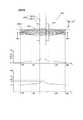
図17は、そのような、基板上の交差部分にのみSiO2膜を形成する従来の光導波路素子の、当該交差部分における基板表面の平面図である。また、図18は図17に示す交差部のXVIII―XVIII断面矢視図、図19の上段の図(上段図)は、図17に示す交差部のXIX−XIX断面矢視図である。また、図19の下段の図(下段図)は、XIX−XIX断面矢視図における光導波路の導波方向に沿った当該光導波路の実効屈折率の変化を示す図である。FIG. 17 is a plan view of the substrate surface at such intersections of a conventional optical waveguide element that forms aSiO 2 film only at such intersections on the substrate. Further, FIG. 18 is a cross-sectional view taken along the line XVIII-XVIII of the intersection shown in FIG. 17, and the upper view (upper view) of FIG. 19 is a cross-sectional view taken along the line XIX-XIX of the intersection shown in FIG. Further, the lower diagram (lower diagram) of FIG. 19 is a diagram showing a change in the effective refractive index of the optical waveguide along the waveguide direction of the optical waveguide in the XIX-XIX cross-sectional arrow view.
図18に示すように、基板2130は、例えば10μmの厚さに薄板化されたLN基板であり、接着層2142を介して支持基板2144上に固定されている。支持基板2144は、例えばガラス基板、LN基板、Si基板等である。 As shown in FIG. 18, the
図17に示すように、基板2130上には、例えばTi熱拡散により形成された図示Y方向に延在する光導波路2134と、例えば金(Au)から成る図示Z方向に延在する電極2136と、が形成されている。光導波路2134と電極2136との交差部2140(図17における図示一点鎖線の矩形で囲まれた部分)には、図18および図19の上段図に示すように、光導波路2134の上部に、バッファ層であるSiO2膜2138が形成され、当該SiO2膜2138の上部に電極2136が形成されている。As shown in FIG. 17, on the
このSiO2膜2138の存在により、交差部2140においては、電極2136の金属Auによる光導波路2134の導波光の光吸収損失が抑制される。Due tothe presence of the SiO 2
しかしながら、このような構成とした場合には、光導波路2134の一部分、すなわち交差部2140に対応する部分にのみ、SiO2膜2138が形成される結果、SiO2膜2138および電極2136からの応力は光導波路2134のうち当該交差部2140に対応する部分に集中して加わることとなる。However, in the case of such a configuration, a portion of the
特に、100Gを超える高速光変調を行う光変調素子では、一般に、信号電極は、その導体損失の低減等を図るべく、その厚さが20μmから40μmと厚く構成される一方、上記のような光吸収損失の低減のために設けられるバッファ層としてのSiO2膜は、その目的に十分な厚さである0.3μmから0.5μmの薄さで形成される。このため、特に、電極2136が信号電極であるような構成においては、電極2136の形成時に金属Auに蓄えられた応力又は電極2136とSiO2膜2138との界面に残存した応力が、1μm以下の薄さで形成されたSiO2膜2138を介して光導波路2134に加わることとなる。 In particular, in an optical modulation element that performs high-speed optical modulation exceeding 100 G, the signal electrode is generally configured to have a thickness of 20 μm to 40 μm in order to reduce the conductor loss, etc., while the above-mentioned light is used. The SiO2 film as a buffer layer provided for reducing the absorption loss is formed with a thickness of 0.3 μm to 0.5 μm, which is a sufficient thickness for the purpose. Therefore, particularly in a configuration in which the
そして、これらの応力は、図19の下段図に示すように、基板2130を構成するLNの光弾性効果を介して、光導波路2134内の実効屈折率n1を、交差部2140において、例えばΔn9だけ増加させて、n9まで急峻に変化させる。なお、図19の下段図において、縦軸は、光導波路2134の実効屈折率neffを示し、横軸は、光導波路2134の導波方向であるY方向における位置を示している。Then, as shown in the lower part of FIG. 19, these stresses are applied to the effective refractive index n1 in the
このような実効屈折率の急峻な変化は、交差部2140において、光導波路2134内の光の伝搬モードに急峻な変化(例えば伝搬モードのモードフィールド径の急峻な変化)を生じさせ、当該交差部2140の境界部分において、当該モードの変化による漏れ光起因する漏れ光を生じさせ得る。その結果、上記のような従来の光導波路素子では、当該漏れ光に起因して、光導波損失の増加や消光比の劣化が発生し得ることとなる。 Such a steep change in the effective refractive index causes a steep change in the propagation mode of light in the optical waveguide 2134 (for example, a steep change in the mode field diameter of the propagation mode) at the
特に、電界効率を高めるべく薄板化された基板を用いる光導波路素子では、より厚い基板を用いる光導波路素子に比べて応力感受性が高く、上記のようなモードの変化による漏れ光に起因する損失増加や消光比の劣化が、より強く発生することとなり得る。また、光導波路2134と電極2136との交差部2140がY字型の光分岐部や光合波部を構成する光導波路部分の近傍にある場合には、上記モードの変化は光分岐比や光合波作用に偏りを生じさせ、消光比に特に大きな影響を与えることとなり得る。 In particular, an optical waveguide element using a thinned substrate to increase electric field efficiency has higher stress sensitivity than an optical waveguide element using a thicker substrate, and an increase in loss due to leakage light due to a mode change as described above. And the deterioration of the extinction ratio may occur more strongly. Further, when the
なお、光導波路2134の、交差部2140における実効屈折率の変化は、交差部2140に加わる応力の方向(基板の結晶軸に対する方向)に依存して、光導波路2134の他の部分の実効屈折率n1に対し増加する場合もあれば、減少する場合もある。すなわち、Δn9の符号は、図19の下段図の例のようにプラス(すなわち、屈折率増加)の場合もあれば、マイナス(すなわち、屈折率減少)の場合もあり得る。交差部2140において実効屈折率が急峻に減少する場合も、上記と同様に、光導波路2134内の伝搬モードの変化に起因して漏れ光が発生し、光導波損失の増加や消光比の劣化が起こり得る。 The change in the effective refractive index of the
本発明に係る光導波路素子は、このような、交差部における伝搬モードの変化に起因して発生し得る当該光導波路素子の光学特性の劣化ないし悪化を招くことなく、当該交差部での電極金属による導波光の光吸収損失を効果的に低減する。 The optical waveguide element according to the present invention does not cause deterioration or deterioration of the optical characteristics of the optical waveguide element that may occur due to such a change in the propagation mode at the intersection, and the electrode metal at the intersection. Effectively reduces the light absorption loss of the waveguide light due to the above.
以下、図面を参照して、本発明の実施の形態を説明する。
[第1の実施形態]
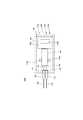
図1は、本発明の第1の実施形態に係る光導波路素子である光変調素子104を用いた光変調器100の構成を示す図である。光変調器100は、筺体102と、当該筺体102内に収容された光変調素子104と、中継基板106と、を有する。光変調素子104は、例えば、DP−QPSK変調器である。筺体102は、最終的にはその開口部に板体であるカバー(不図示)が固定されて、その内部が気密封止される。Hereinafter, embodiments of the present invention will be described with reference to the drawings.
[First Embodiment]
FIG. 1 is a diagram showing a configuration of an
光変調器100は、また、光変調素子104の変調に用いる高周波電気信号を入力するための信号ピン110a、110b、110c、110dと、これらの信号ピン110a、110b、110c、110dを筺体102内に導入するためのフィードスルー部108と、を有する。 The
さらに、光変調器100は、筺体102内に光を入力するための入力光ファイバ114と、光変調素子104により変調された光を筺体102の外部へ導く出力光ファイバ120と、を筺体102の同一面に有する。 Further, the
ここで、入力光ファイバ114及び出力光ファイバ120は、固定部材であるサポート122及び124を介して筺体102にそれぞれ固定されている。入力光ファイバ114から入力された光は、サポート122内に配されたレンズ130によりコリメートされた後、レンズ134を介して光変調素子104へ入力される。ただし、これは一例であって、光変調素子104への光の入力は、従来技術に従い、例えば、入力光ファイバ114を、サポート122を介して筺体102内に導入し、当該導入した入力光ファイバ114の端面を光変調素子104の基板230の端面に接続することで行うものとすることもできる。 Here, the input
光変調器100は、また、光変調素子104から出力される2つの変調された光を偏波合成する光学ユニット116を有する。光学ユニット116から出力される偏波合成後の光は、サポート124内に配されたレンズ118により集光されて出力光ファイバ120へ結合される。 The
中継基板106は、当該中継基板106に形成された導体パターン(不図示)により、信号ピン110a、110b、110c、110dから入力される高周波電気信号を光変調素子104へ中継する。中継基板106上の上記導体パターンは、例えばワイヤボンディング等により、光変調素子104の信号電極の一端を構成するパッド(後述)にそれぞれ接続される。また、光変調器100は、所定のインピーダンスを有する2つの終端器112aおよび112bを筺体102内に備える。 The
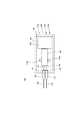
図2は、図1に示す光変調器100の筺体102内に収容される光導波路素子である光変調素子104の、構成の一例を示す図である。光変調素子104は、例えばLNで構成される基板230上に形成された光導波路(図示太線の点線)で構成され、例えば200GのDP−QPSK変調を行う。これらの光導波路は、基板230の表面にTiを熱拡散することにより形成されるものとすることができる。 FIG. 2 is a diagram showing an example of the configuration of the
基板230は、例えば矩形であり、図示上下方向に延在して対向する図示左右の2つの辺280a、280b、および図示左右方向に延在して対向する図示上下の辺280c、280dを有する。なお、図2においては、図示左上部に示す座標軸に示すとおり、図2の紙面の奥へ(オモテ面からウラ面へ)向かう法線方向をX方向、図示右方向をY方向、図示下方向をZ方向とする。 The
光変調素子104は、基板230の図示左方の辺280bの図示下側において入力光ファイバ114からの入力光(図示右方を向く矢印)を受ける入力導波路232と、入力された光を同じ光量を有する2つの光に分岐する分岐導波路234と、を含む。また、光変調素子104は、分岐導波路234により分岐されたそれぞれの光を変調する2つの変調部である、いわゆるネスト型マッハツェンダ型光導波路240a、240b(それぞれ、図示一点鎖線で囲まれた部分)を含む。 The
ネスト型マッハツェンダ型光導波路240a、240bは、それぞれ、一対の並行導波路を成す2つの導波路部分に設けられたそれぞれ2つのマッハツェンダ型光導波路244a(図示破線内部分)、246a(図示二点鎖線内部分)、および244b(図示破線内部分)、246b(図示二点鎖線内部分)を含む。これにより、ネスト型マッハツェンダ型光導波路240a、240bは、光分岐導波路23により2つに分岐された入力光のそれぞれをQPSK変調した後、変調後の光(出力)をそれぞれの出力導波路248a、248bから図示左方へ出力する。 Each of the nested Machzenda type
これら2つの出力光は、その後、基板230外に配された光学ユニット116により偏波合成されて一つの光ビームにまとめられる。以下、光変調素子104の基板230上に形成された入力導波路232、分岐導波路234、並びにネスト型マッハツェンダ型光導波路240a、240b及びこれらに含まれるマッハツェンダ型光導波路244a、246a、244b、246bを、総称して光導波路232等ともいうものとする。 These two output lights are then polarized and combined by an
基板230上には、ネスト型マッハツェンダ型光導波路240a、240bを構成する合計4つのマッハツェンダ型光導波路244a、246a、244b、246bのそれぞれに変調動作を行わせるための信号電極250a、252a、250b、252bが設けられている。信号電極250a、252aは、図示左方が屈曲して、基板230の図示上方の辺280cまで延在し、パッド254a、256aに接続されている。また、信号電極250a、252aの図示右方は、基板230の図示右方の辺280aまで延在し、パッド258a、260aに接続されている。 On the
同様に、信号電極250b、252bの図示左方は、基板230の図示下方の辺280dまで延在して、パッド254b、256bに接続され、信号電極250b、252bの図示右方は、基板230の図示右方の辺280aまで延在し、パッド258b、260bに接続されている。パッド258a、260a、258b、260bは、ワイヤボンディング等により、上述した中継基板106と接続される。 Similarly, the left side of the
なお、信号電極250a、252b、250b、252bは、従来技術に従い、基板230上に形成されたグランド導体パターン(不図示)と共に、例えば、所定のインピーダンスを有するコプレーナ伝送線路を構成している。グランド導体パターンは、例えば、光導波路232等の上には形成されないように設けられ、グランド導体パターンのうち光導波路232等により分割されて形成される複数の領域間は、例えばワイヤボンディング等により互いに接続されるものとすることができる。 The
パッド254a、256aおよび254b、256bは、上述した終端器112aおよび112bに接続される。これにより、パッド258a、260a、258b、260bに接続された中継基板106から入力される高周波電気信号は、進行波となって信号電極250a、252a、250b、252bを伝搬し、マッハツェンダ型光導波路244a、246a、244b、246bを伝搬する光波をそれぞれ変調する。 The
ここで、信号電極250a、252a、250b、252bが基板230内に形成する電界と、マッハツェンダ型光導波路244a、246a、244b、246bを伝搬する導波光と、の相互作用をより強めて高速変調動作をより低電圧で行い得るように、基板230は、20μm以下の厚さ、好適には10μm以下の厚さに形成される。なお。基板230は、その裏面(図2に示す面に対向する面)が、接着層を介してガラス等の支持基板に接着されている(図2では不図示。後述する図4等において、接着層490および支持基板492として記載)。 Here, the high-speed modulation operation is performed by further strengthening the interaction between the electric field formed by the
光変調素子104には、また、いわゆるDCドリフトによるバイアス点の変動を補償するためのバイアス電極262a、264a、および262b、264bが設けられている。バイアス電極262a、262bは、それぞれ2組の電極ペアで構成されており、それぞれ、マッハツェンダ型光導波路244a、246aおよび244b、246bのバイアス点変動の補償に用いられる。また、バイアス電極264aおよび264bは、それぞれ、ネスト型マッハツェンダ型光導波路240aおよび240bのバイアス点変動の補償に用いられる。 The
これらのバイアス電極262a、264a、および262b、264bも、それぞれ、基板230の辺280cおよび280dまで延在し、当該辺280cおよび280dの近傍部分において、例えば筺体102の底面に設けられたリードピン(不図示)を介して、筺体外部のバイアス制御回路と接続される。これにより、当該バイアス制御回路によりバイアス電極262a、264a、262b、264bが駆動されて、対応する各マッハツェンダ型光導波路のバイアス点変動が補償される。以下、信号電極250a、252a、250b、252bおよびバイアス電極262a、264a、262b、264bを、総称して電極250a等という。 These
上記のように構成される光変調素子104は、光導波路232等と電極250a等とが交差する多くの交差部分を含んでいる。図2の記載から容易に理解されるように、図2において光導波路232等を示す図示太線点線と電極250a等を示す図示帯状部分とが交差する部分は、すべて、光導波路232等と電極250a等とが交差する交差部分である。本実施形態では、光変調素子104は、全部で50箇所の交差部分を含んでいる。 The
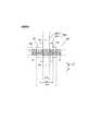
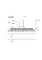
図3、図4、および図5は、そのような交差部分の構成の第1の例としての、入力導波路232と信号電極250bとが交差する図2におけるA部の構成を示す部分詳細図である。ここに、図3は、A部の平面図、図4は、図3に示すA部のIV−IV断面矢視図である。また、図5の上段図は、図3に示すA部のV−V断面矢視図であり、図5の下段図は、図5の上段図に対応して描かれた、入力導波路232の導波方向に沿った当該入力導波路232内部の実効屈折率の変化を示す図である。図3、図4、及び図5は、従来技術における交差部分を描いた図17、図18、および図19に対応する図である。 3, FIG. 4, and FIG. 5 are partial detailed views showing the configuration of part A in FIG. 2 where the
なお、図3、図4、図5に示す構成は、光変調素子104における光導波路232等と電極250a等とが交差する部分の構成の一例であって、A部以外の、光導波路232等と電極250a等とが交差する任意の部分にも同様に用いることができる。 The configuration shown in FIGS. 3, 4, and 5 is an example of the configuration of the portion where the
図3において、図示左右方向(Y方向)に延在する入力導波路232と、図示上下方向(Z方向)に延在する信号電極250bとは、互いに交差して、交差部370(図示一点鎖線の矩形で囲まれた部分)を形成している。図4において、基板230は、接着層490を介して支持基板492に固定されている。ここで、接着層490は、例えば熱硬化性樹脂等で構成され、支持基板492は、例えばガラス基板、LN基板、Si基板等で構成される。 In FIG. 3, the
そして、交差部370において、信号電極250bは、金属材料から成る複数の金属層450−1、450−2を含む多層構造をなし、信号電極250bと基板230との間には樹脂材料から成る樹脂層452が形成されている。なお、上記多層構造をなす金属層の数は2つに限らず3つ以上でもよい。また、樹脂層も、少なくとも1つあればよく、2つ以上の数であってもよい。 Then, at the
また、上記複数の金属層450−1と450−2とは、互いに種類の異なる金属であってもよいし、同種の金属であってその金属層の製法が互いに異なるものであってもよい(3つ以上の金属層を含む場合も同様である)。例えば金属層450−1と450−2とを互いに異なる種類の金属とする場合、金属層450−1をチタン(Ti)、金属層450−2を金(Au)で構成するものとしてもよい。また金属層450−1と450−2とが同種の金属であって、その金属層の製法が互いに異なる場合、金属層450−1は、スパッタで形成された金(Au)で構成され、金属層450−2は、電界メッキにより形成された金(Au)で構成されてもよい。なお、金属層450−1と450−2との境界面が応力を分散するという観点からすると金属層450−1と450−2など境界線を形成する2つの金属層が互いに異なる種類の金属とする方が望ましい。 Further, the plurality of metal layers 450-1 and 450-2 may be different types of metals, or may be the same type of metal and the manufacturing methods of the metal layers may be different from each other (). The same applies when three or more metal layers are included). For example, when the metal layers 450-1 and 450-2 are made of different types of metals, the metal layer 450-1 may be made of titanium (Ti) and the metal layer 450-2 may be made of gold (Au). Further, when the metal layers 450-1 and 450-2 are the same type of metal and the manufacturing methods of the metal layers are different from each other, the metal layer 450-1 is composed of gold (Au) formed by sputtering and is a metal. Layer 450-2 may be made of gold (Au) formed by electroplating. From the viewpoint that the interface between the metal layers 450-1 and 450-2 disperses stress, the two metal layers forming the boundary line, such as the metal layers 450-1 and 450-2, are different types of metals. It is better to do it.
なお、金属層450−1及び450−2を含む信号電極250bは、変調速度が100Gbpsを超える広帯域動作を行う光変調素子104では、一般に、その全体の厚さが20μmから40μmの範囲となるように形成される。また、一般に、金属層450−1は、金属層450−2を形成するための下地層として厚さ0.1〜0.3μm程度に形成される。すなわち、信号電極250bの厚さは、金属層450−2の厚さでほぼ定まる。したがって、信号電極250bから基板230へかかる応力の主たる発生要因は、上部の金属層450−2である。なお、バイアス電極262a、262b、264a、264bは、一般に、全体の厚さが1μmから5μmの範囲で形成され、この場合にも、これらバイアス電極を構成する下地金属層は、厚さ0.1〜0.3μm程度で形成されるのが一般的である。したがって、バイアス電極の場合も、上部の金属層が基板230への応力の主たる発生要因となる。 The
図5の上段図に示すように、本実施形態では、信号電極250bの金属層450−1と450−2とは同じ幅Leで形成され、樹脂層452の幅Ly1は、これら金属層の幅Leと同じ幅となっている。ただし、これは一例であって、樹脂層452の幅Ly1は、その上部の金属層450−1が入力導波路232と接触しないように、金属層450−1の幅よりも大きい任意の幅とすることができる。また、上部の金属層450−2の幅は、下部の金属層450−1の幅よりも小さく形成されていてもよいし、大きく形成されるものとすることもできる。 As shown in the upper part of FIG. 5, in the present embodiment, the metal layers 450-1 and 450-2 of the
図5の下段図は、図5の上段図に示す構成における、入力導波路232の導波方向(Y方向)に沿った当該入力導波路232の実効屈折率の変化を示す図である。図19の下段図と同様に、図5の下段図における縦軸は、入力導波路232の実効屈折率neffを示し、横軸は、入力導波路232の導波方向であるY方向における位置を示している。The lower diagram of FIG. 5 is a diagram showing a change in the effective refractive index of the
図5の上段図に示すとおり、交差部370には、金属層450−1と基板230との間に樹脂層452が形成されていることから、当該交差部370において入力導波路232を伝搬する導波光に金属層450−1に起因する光吸収損失が発生することが防止される。また、交差部370における信号電極250aが複数の金属層450−1、450−2を含む多層構造で構成され、信号電極250aと基板230との間に樹脂層452があることにより、当該交差部370において上部の金属層450−2から入力導波路232に伝わる応力は、当該金属層450−2と下部の金属層450−1との界面及び又は当該下部の金属層450−1により緩和される共に、剛性の低い樹脂層452により更に緩和される。このため、光変調素子104では、基板230の全面又は交差部分にSiO2から成るバッファ層を形成する従来の光導波路素子に比べて、基板230の交差部370の部分に加わる応力が緩和される。As shown in the upper part of FIG. 5, since the
したがって、光変調素子104では、図5の下段図に示すように、交差部370における入力導波路232の実効屈折率の変化量Δn4は、バッファ層としてSiO2を用いる従来技術の構成における値(図19に示すΔn9)に比べて小さく抑制され、当該交差部370において発生し得る入力導波路232での導波光の伝搬モードの変化の程度も緩和され得る。 Therefore, in the
その結果、光変調素子104では、交差部370における上記伝搬モードの変化に起因する漏れ光の発生等を抑制して、光学特性の劣化ないし悪化を防止ないし抑制しつつ、信号電極250bによる光吸収損失を効果的に低減することができる。 As a result, in the
上述したように、図3、図4、図5に示す構成は、A部以外の、光導波路232等と電極250a等とが交差する他の交差部分にも同様に適用することができる。すなわち、光変調素子104では、電極金属に起因する光吸収損失について求められる抑制の程度や、消光比劣化の抑制のために求められる漏れ光抑制の程度に応じて、光導波路232等と電極250a等との交差部分の全部又は一部について、図3、図4、図5に示す構成と同様の構成を適用することができる。 As described above, the configuration shown in FIGS. 3, 4, and 5 can be similarly applied to other intersections other than the part A where the
なお、上記の構成において、樹脂層452を構成する樹脂は、例えば、架橋反応により形成される樹脂であるものとすることができる。このような樹脂は、例えば、架橋剤を含む高分子材料で構成され、当該高分子材料を加熱加工することにより形成され得る。また、樹脂層452を構成するそのような樹脂は、SiO2のヤング率72GPaから74GPaに対し一桁小さい1から2GPaの低ヤング率を有するものとして形成され得る。In the above configuration, the resin constituting the
また、図3、図4、図5に示す構成においては、樹脂層452は、その平面視が、長さLzと幅Ly1を持つ、信号電極250bに沿って長い矩形(すなわち、Lz>Ly1)として形成されているが(図3参照)、これには限られない。樹脂層452の平面視は、交差部370を覆い得るサイズである限りにおいて、入力導波路232に沿って長い矩形(すなわち、Lz<Ly1)として形成されていてもよい。 Further, in the configurations shown in FIGS. 3, 4, and 5, the
また、交差部分の一例として示した図2のA部においては、入力導波路232と信号電極250bとの交差角度は直角であるものとしたが、これには限られない。当該交差角度は任意の角度であるものとすることができ、樹脂層452の平面視形状は、入力導波路232と信号電極250bとが交差する部分を覆い得るサイズである限りにおいて任意の形状であるものとすることができる。 Further, in the part A of FIG. 2 shown as an example of the intersecting portion, the intersecting angle between the
また、図3ないし図5に示す構成においては、信号電極250bは、2つの金属層450−1、450−2で構成されるものとしたが、これには限られない。信号電極250bは、上述したように、3つ以上の金属層で形成されていてもよい。例えば、交差部370における信号電極は、図6に示す信号電極250b´のように、4つの金属層650−1、650−2、650−3、650−4で構成されるものとすることができる。この場合、相接する少なくとも2つの金属層は、相異なる種類の金属又は相異なる方法で形成された同種の金属で構成されるものとすることができる。 Further, in the configurations shown in FIGS. 3 to 5, the
このような構成では、金属層650−1、650−2、650−3、650−4が形成する金属層間の界面において、より上部に形成された金属層からの応力がより下部に形成された金属層へ伝搬するのを抑制することができる。また、このような構成においては、金属層一層あたりの厚さを、より少ない数の層で構成される電極に比べて薄くできるため、各金属層の内部に発生し得る応力自体をより低減することができる。その結果、図6に示す構成では、信号電極250b´から基板230へ加わる応力がさらに緩和され得る。 In such a configuration, at the interface between the metal layers formed by the metal layers 650-1, 650-2, 650-3, 650-4, the stress from the metal layer formed at the upper part is formed at the lower part. Propagation to the metal layer can be suppressed. Further, in such a configuration, the thickness per metal layer can be made thinner than that of an electrode composed of a smaller number of layers, so that the stress itself that can be generated inside each metal layer can be further reduced. be able to. As a result, in the configuration shown in FIG. 6, the stress applied from the signal electrode 250b'to the
なお、電極250a等と光導波路232等との交差部において電極250a等が3つ以上の金属層を含む多層構造で構成されている場合、基板230に最も近い金属層(例えば650−1)である最下層を除く上記金属層の少なくとも一つ(例えば650−4)が、当該最下層より厚く構成されていることが望ましい。これにより、最下層より厚く構成された金属層の内部応力は、これより薄く構成された最下層と上部の金属層との界面において効果的に分散され、基板230上の光導波路232等へ加わる応力及び当該応力に起因する屈折率変化が効果的に緩和される。 When the
また、図6に示す構成では、金属層650−1、650−2、650−3、650−4は、同じ幅で構成されるものとしたが、これには限られない。金属層650−1、650−2、650−3、650−4は、その全部又は一部が互いに異なる幅で形成されるものとすることができる。 Further, in the configuration shown in FIG. 6, the metal layers 650-1, 650-2, 650-3, and 650-4 are configured to have the same width, but the present invention is not limited to this. The metal layers 650-1, 650-2, 650-3, 650-4 may be formed in whole or in part having different widths from each other.
次に、本実施形態に係る光変調器100の光変調素子104に用いられる、光導波路232等と電極250a等との交差部分の第2の構成例について説明する。 Next, a second configuration example of the intersection of the
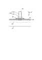
図7、図8、および図9は、交差部分の第2の構成例を示す図であり、具体的には、図2示す入力導波路232と信号電極252bとが交差するB部の構成を示す部分詳細図である。ここに、図7は、図2に示すB部の平面図、図8は、図7に示すB部のVIII−VIII断面矢視図である。また、図9の上段図は、図7に示すB部のIX−IX断面矢視図であり、図9の下段図は、入力導波路232の導波方向に沿った当該入力導波路232内部の実効屈折率の変化を示す図である。すなわち、図7、図8、図9の上段図、及び図9の下段図は、それぞれ、図2のA部について示した図3、図4、図5の上段図、及び図5の下段図に相当する。また、図9の中段図は、入力導波路232の導波方向(本実施形態ではY方向)に沿った当該入力導波路232に加わる応力の変化を示す図である。図9の中段図には、比較のため、図3ないし図5に示すA部の構成において入力導波路232にかかる応力のピーク値のレベルが、値p4として記載されている。 7, FIG. 8 and FIG. 9 are views showing a second configuration example of the intersecting portion. Specifically, the configuration of the B portion where the
なお、図7、図8、図9において、図3、図4、図5に示す構成要素と同じ構成要素については、図3、図4、図5における符号と同じ符号を用いて示すものとし、上述した図3、図4、図5についての説明を援用する。 Note that, in FIGS. 7, 8 and 9, the same components as those shown in FIGS. 3, 4 and 5 shall be shown using the same reference numerals as those shown in FIGS. 3, 4 and 5. , The above description of FIGS. 3, 4, and 5 is incorporated.
また、図7、図8、図9に示すB部の構成は、光変調素子104における光導波路232等と電極250a等とが交差する部分の構成の他の一例であって、図3、図4、図5に示す構成に代えてA部に用いることもできるし、A部及びB部以外の、光導波路232等と電極250a等とが交差する他の任意の部分に、同様に適用することができる。 Further, the configuration of the portion B shown in FIGS. 7, 8 and 9 is another example of the configuration of the portion where the
図7において、図示左右方向(Y方向)に延在する入力導波路232と、図示上下方向(Z方向)に延在する信号電極252bとは、互いに交差して、交差部770を形成している。 In FIG. 7, the
B部の交差部770においては、図3、図4に示したA部の交差部370と同様に、信号電極252bが、複数の金属層850−1、850−2を含む多段構成をなし、信号電極252bと基板230との間には樹脂材料から成る樹脂層852が形成されている。ただし、図9の上段図に示すように、B部の構成は、図5の上段図に示したA部の構成とは異なり、金属層850−1、850−2、及び樹脂層852の、入力導波路232の導波方向に沿った長さが、互いに異なっている。 In the
具体的には、樹脂層852は、入力導波路232の導波方向(又は延在方向(本実施形態ではY方向))に沿った長さLy2が、隣接する金属層850−1の、入力導波路232の導波方向に沿った長さLe1より長くなるように形成されている。また、樹脂層852に隣接する金属層850−1は、入力導波路232の導波方向に沿った長さLe1が、当該金属層850−1に隣接する他の金属層850−2の、入力導波路232の導波方向に沿った長さLe2より長くなるように形成されている。すなわち、Le2<Le1<Lyである。 Specifically, in the
上記の構成では、Le2<Le1<Lyであることから、下部の金属層850−1よりも一般に厚く形成されて主たる応力発生要因となり得る金属層850−2から基板230へ伝わる応力は、Le2より長く形成される下部の金属層850−1及び樹脂層852により分散されて基板230へ到達することなる。同様に、金属層850−1から基板230への応力は、Le1より長く形成される樹脂層852により分散されて基板230へ到達することなる。このため、交差部770において基板230にかかる応力のピーク値は、図5に示す交差部370におけるピーク値p4から減少してp3となる。したがって、交差部770において入力導波路232に発生する実効屈折率の変化も緩やかとなり、実効屈折率のピーク値は、図5に示す交差部370におけるピーク値n4から減少してn3となる。 In the above configuration, since Le2 <Le1 <Ly, the stress transmitted from the metal layer 850-2 to the
また、上記の構成においては、Le2<Le1<Lyであることから、交差部770において基板230へ加わる応力の、入力導波路232の導波方向に沿った変化は、図9の中段図に示すように階段状となる。このため、交差部770において入力導波路232に発生する実効屈折率の変化も、図9の下段図に示すように階段状となり、入力導波路232の延在方向における実効屈折率の変化は、実効屈折率のピーク値が単に減少した場合よりも更に緩やかとなる。 Further, in the above configuration, since Le2 <Le1 <Ly, the change in the stress applied to the
したがって、交差部770において発生し得る入力導波路232の導波光の伝搬モードの変化も緩やかとなり、交差部770を含むB部において入力導波路232の導波光の伝搬モードの変化に起因して発生し得る漏れ光の量は、図3ないし図5に示すA部におけるよりも低減され得る。その結果、図7ないし図9に示すB部の構成においては、図3ないし図5に示すA部の構成に比べて、漏れ光の発生に起因する光変調素子104の光学特性等の悪化や劣化への影響を更に低減することができる。 Therefore, the change in the propagation mode of the waveguide light of the
なお、上述したB部の構成においては、Le2<Le1<Lyであるものとしたが、これには限られない。例えば、樹脂層852の長さLy2が、隣接する金属層850−1の長さLe1より長くなるように形成されている限りにおいて、樹脂層852に隣接する金属層850−1は、その長さLe1が、当該金属層850−1に隣接する他の金属層850−2の長さLe2と等しく形成されていてもよい(すなわち、Le2=Le1<Ly2)。このような構成でも、金属層850−1及び850−2の長さよりも長く形成される樹脂層852により、金属層850−1、850−2からの応力が分散されて基板230へ伝わるので、交差部770における入力導波路232の実効屈折率をある程度低減して、漏れ光の発生を抑制することができる。 In the configuration of the B portion described above, Le2 <Le1 <Ly is assumed, but the present invention is not limited to this. For example, as long as the length Ly2 of the
なお、上記のように基板230ないし光導波路232に加わる応力の階段状の位置変化に応じて光導波路232における実効屈折率を効果的に変化させるためには、上記応力の階段状変化の距離を、光導波路232を伝搬する光の波長以上とすることが望ましい。したがって、望ましくは、樹脂層852のうち、当該樹脂層852に隣接する金属層850−1が形成されていない部分は、光導波路232の導波方向に沿った長さLe11及び又はLe12(図9参照)が、光導波路232を伝搬する光の波長λより長く構成される(すなわち、Le11,Le12≧λ)。また、望ましくは、樹脂層852に隣接する金属層850−1のうち、金属層850−1に隣接する他の金属層850−2が形成されていない部分は、光導波路232の導波方向に沿った長さL21及び又はL22が、光導波路232を伝搬する光の波長λより長く構成されている(すなわち、Le21,Le22≧λ)。 In order to effectively change the effective refractive index of the
なお、A部の構成についての説明において上述したとおり、交差部における電極250a等は2つ以上の複数の金属層で構成されているものとすることができる。例えば、上記B部の構成において、信号電極252bは、金属層850−2の上部に設けられた第3の金属層を有していてもよい。また、上記の効果は、当該第3の金属層の上記導波方向に測った長さがLe2より長い場合でも、同様に奏することができる。 As described above in the description of the configuration of the A portion, the
また、上述したB部における構成において、信号電極252bから基板230へ伝わる応力を更に低減すべく、金属層850−1にスリットを設けるものとしてもよい。図10は、そのような、スリット1054を設けて構成された金属層850−1´を用いた、B部の代替構成を示す図であり、図9の上段図に相当する図である。図10において、図9の上段図と同じ構成要素については図9の上段図と同じ符号を用いている。 Further, in the above-described configuration of the B portion, a slit may be provided in the metal layer 850-1 in order to further reduce the stress transmitted from the
図10において、スリット1054の内部は、例えば空洞である。金属層850−1´にスリット1054を設けることにより、その上部の金属層850−2から伝わる応力は、スリット1054において開放されることとなるので、金属層850−2から基板230へ伝わる応力は、図7ないし図9に示す構成に比べて更に低減される。その結果、当該応力に起因して発生する入力導波路232における実効屈折率の変化は更に緩やかとなり、B部から発生する漏れ光が更に低減され、当該漏れ光による光変調素子104の光学特性の悪化が更に抑制される。 In FIG. 10, the inside of the
なお、スリット1054の、信号電極250bの延在方向に沿った長さは、応力開放の観点から、入力導波路232の幅以上であることが望ましい。また、図10に示す構成では、金属層850−1´に形成されるスリット1054は、金属層850−1´の厚さ方向の途中まで設けられるものとしたが、これには限られない。スリット1054は、樹脂層852の表面に達するまで金属層850−1´を貫通して設けられるものとしてもよい。 The length of the
また、スリット1054は、図10に示す構成においては、樹脂層852と金属層850−2の2つの層に挟まれた金属層850−1´に形成されるものとしたが、これには限られない。スリット1054のようなスリットは、例えば信号電極252b´が3つ以上の金属層で構成されている場合には、任意の2つの層(上記3つ以上の金属層及び基板230上の樹脂層を含む、任意の2つの層)に挟まれた金属層に設けられるものとすることができる。すなわち、スリットは、信号電極252b´の多層構造を構成する金属層のうち、最も上部に形成された金属層を除く少なくとも一つの金属層に形成されているものとすることができる。 Further, in the configuration shown in FIG. 10, the
また、図9の上段図に示すB部の構成において、入力導波路232の実効屈折率の変化を更に緩やかにする構成として、樹脂層852の左右の両端部の厚さを、交差部770から離れるに従って薄く構成してもよい。図11は、そのような、入力導波路232の導波方向に沿った両端部において交差部770から離れるに従ってより薄く形成された樹脂層852´を用いる、B部の他の代替構成を示す図であり、図9の上段図に相当する図である。図11において、図9の上段図と同じ構成要素については図9の上段図と同じ符号を用いている。 Further, in the configuration of the portion B shown in the upper part of FIG. 9, the thickness of both left and right ends of the
図11に示す構成においては、樹脂層852´の両端部の厚さが、交差部770から離れるに従って薄くなっているため、これらの両端部を介して基板230へ加わる応力は、交差部770から離れるに従って低下する。このため、当該両端部における入力導波路232の実効屈折率の変化は、図9に示す構成における樹脂層852の両端部における実効屈折率の変化よりも緩やかとなる。 In the configuration shown in FIG. 11, since the thickness of both ends of the resin layer 852'becomes thinner as the distance from the
このため、図11に示す構成では、図9の上段図に示す構成に比べて、B部における入力導波路232の伝搬モードの変化が緩やかとなり、B部における漏れ光の発生が更に抑制される。その結果、図11に示す構成では、図9の上段図に示す構成に比べて、B部において発生し得る漏れ光に起因する光変調素子104の光学特性の悪化を更に抑制することができる。なお、図11に示す樹脂層852´のような形状は、樹脂層852´の形成過程において加熱処理の時間を通常より長く及び又は加熱温度を通常より高くして、樹脂層852´を構成する樹脂の、硬化前の粘性を高めることで容易に形成することができる。 Therefore, in the configuration shown in FIG. 11, the change in the propagation mode of the
また、上記樹脂に架橋剤を含有させ、架橋反応させることによっても図11に示す樹脂層852´のような形状を容易に形成する事ができる。なお、図11では樹脂層852´の厚さが、交差部770から薄くなり始めているが、これに限られない。例えば樹脂層852´の厚さは交差部770から一定の範囲まではほぼ同じ厚さで、その後、徐々に薄くなるようにしてもよい。 Further, by incorporating a cross-linking agent into the resin and causing a cross-linking reaction, a shape like the resin layer 852'shown in FIG. 11 can be easily formed. In FIG. 11, the thickness of the resin layer 852'begins to decrease from the
次に、本実施形態に係る光変調器100の光変調素子104に用いられる、光導波路232等と電極250a等との交差部分の第3の構成例について説明する。 Next, a third configuration example of the intersection between the
図12および図13は、交差部分の第3の構成例を示す図であり、具体的には、図2示すマッハツェンダ型光導波路244bの並行導波路を構成する一方の光導波路244b−1と信号電極252bとが交差するC部の構成を示す部分詳細図である。ここに、図12の上段図は、C部の平面図、図12の中段図は、光導波路244b−1の導波方向(本実施形態ではY方向)に沿った当該光導波路244b−1に加わる応力の変化を示す図、図12の下段図は、光導波路244b−1の導波方向に沿った当該光導波路244b−1の内部の実効屈折率の変化を示す図である。また、図13は、図12の上段の図におけるXIII−XIII平面矢視図である。 12 and 13 are views showing a third configuration example of the intersection, and specifically, a signal with one of the
図12の上段図は、A部及びB部についてそれぞれ示した図3および図7に相当する。また、図12の中段図は、B部について示した図9の中段図に相当し、図12の下段図は、図9の下段図に相当する。また、図13は、A部及びB部についてそれぞれ示した図5および図9の上段の図に相当する。 The upper part of FIG. 12 corresponds to FIGS. 3 and 7, respectively, showing the parts A and B, respectively. Further, the middle diagram of FIG. 12 corresponds to the middle diagram of FIG. 9 showing the portion B, and the lower diagram of FIG. 12 corresponds to the lower diagram of FIG. 9. Further, FIG. 13 corresponds to the upper view of FIGS. 5 and 9 showing the parts A and B, respectively.
なお、図12及び図13において、図3ないし図11に示す構成要素および値と同じ構成要素および値については、図3ないし図11における符号と同じ符号を用いて示すものとし、上述した図3ないし図11についての説明を援用する。 In addition, in FIGS. 12 and 13, the same components and values as those shown in FIGS. 3 to 11 are shown using the same reference numerals as those shown in FIGS. 3 to 11, and FIG. 3 described above. Alternatively, the description of FIG. 11 is incorporated.
なお、図12および図13に示すC部の構成は、光導波路232等と電極250a等とが交差する部分の構成の一例であって、図3ないし図5に示す構成に代えてA部に用いることもできるし、図7ないし図9に示す構成に代えてB部に用いることもできる。また、図12および図13に示すC部の構成は、A部およびB部以外の、光導波路232等と電極250a等との他の任意の交差部分にも同様に適用することができる。 The configuration of the C portion shown in FIGS. 12 and 13 is an example of the configuration of the portion where the
図12の上段図において、図示左右方向(Y方向)に延在する光導波路244b−1と、図示上下方向(Z方向)に延在する信号電極252bとは、互いに交差して、交差部1270を形成している。図13において、C部の交差部1270における信号電極252bの構成は、図9の上段図に示したB部の交差部770における信号電極252bの構成と同様に、複数の金属層1350−1、1350−2を含む多段構成をなす。ただし、図12の上段図に示すように、交差部1270においては、下部の金属層1350−1と基板230との間には、図9の上段図に示す樹脂層852とは異なる形状を持つ樹脂層1352が形成されている。なお、金属層1350−1および1350−2は、信号電極252bの一部として、図9の上段図に示す金属層850−1及び850−2と、それぞれ電気的につながっている。 In the upper view of FIG. 12, the
樹脂層1352は、図9の上段図に示す樹脂層852と同様に一様な厚さを有するが、その平面視が、矩形で構成される樹脂層852とは異なる(図7および図12の上段図を参照)。すなわち、樹脂層1352は、図12の上段図に示すように、光導波路244b−1の導波方向(すなわち、図示左右方向)に沿った両端部において、当該導波方向に直交する方向の幅が、光導波路244b−1の幅以下であって且つ交差部1270から離れるに従ってより狭く形成されている。具体的には、樹脂層1352は、例えば、導波方向の両端部(図12の上段図の図示左右の端部)に頂点を持つ多角形を平面視形状とする。 The
図12の中段図および下段図には、交差部1270から離れるに従って樹脂層1352の幅が光導波路244b−1の幅より狭く構成された領域が、Y軸方向における位置y90からy92までの領域及び位置y94からy96までの領域として示されている。 In the middle and lower views of FIG. 12, a region in which the width of the
これらの領域では、光導波路244b−1の幅方向において樹脂層1352が当該光導波路244b−1を覆う範囲は、導波方向(Y軸方向)に沿って変化する。このため、樹脂層1352を介して信号電極252bから基板230の光導波路244b−1の部分に加わる応力も、導波方向(Y軸方向)に沿って変化する。 In these regions, the range in which the
具体的には、光導波路244b−1の部分に加わる応力は、図12の中段図に示すように、導波光の伝搬方向(図示右から左へ向かう方向)に沿って、y96からy94へ向かって徐々に増加し、y92からy90に向かって徐々に減少する。したがって、光導波路244b−1の実効屈折率も、光弾性効果により、図12の下段に示すようにy96からy94へ向かって徐々に増加し、y92からy90に向かって徐々に減少する。その結果、位置y96から位置y90に至るまでの範囲における光導波路244b−1の実効屈折率の変化は、図3ないし図5に示すA部および図6ないし図8に示すB部における入力導波路232の実効屈折率の変化より更に緩やかとなり、導波光の伝搬モードの変化も更に緩やかとなる。 Specifically, the stress applied to the portion of the
また、樹脂層1352が光導波路244b−1を覆う範囲は、図7ないし図9に示すB部において樹脂層852が入力導波路232を覆う範囲に比べて広いため、光導波路244b−1に加わる応力のピーク値p2は、B部における入力導波路232の応力のピーク値p3よりも小さくなり(図12の中段図参照)、光導波路244b−1の実効屈折率のピーク値n2も、B部における入力導波路232の実効屈折率のピーク値n3よりも小さくなる(図12の下段図参照)。 Further, since the range in which the
したがって、光導波路244b−1のC部における伝搬モードの変化は、入力導波路232のB部における伝搬モードの変化より緩やかとなる。その結果、伝搬モードの変化に起因するC部における漏れ光の発生の程度は、A部およびB部よりも更に抑制されることとなり、当該漏れ光の発生を介した光変調素子104への光学特性等への影響が更に低減され得る。 Therefore, the change in the propagation mode in the C portion of the
なお、図12の上段図には、一例として、上記導波方向の両端部(図示左右の端部)に頂点を持つ多角形を平面視形状とする樹脂層1352を示したが、樹脂層1352の形状は、これには限られない。樹脂層1352は、光導波路244b−1の導波方向に沿った両端部において、当該導波方向に直交する方向の幅が、光導波路244b−1の幅以下であって且つ交差部1270から離れるに従ってより狭く形成されている限りにおいて、他の形状で構成されるものとすることができる。そのような形状は、例えば、図示左右の端部が曲線で構成された形状であってもよい。なお、樹脂層1352の端部だけでなく、樹脂層1352の他の角部も、曲線で構成されるものとすることができる。 In the upper part of FIG. 12, as an example, a
図14は、そのような、端部が曲線で構成された平面視形状を有する樹脂層1352´を用いた、C部の代替構成を示す図であり、図12の上段図に相当する図である。図14において、図12および図13と同じ構成要素については図12及び図13における符号と同じ符号を用いている。図14に示す構成においても、樹脂層1352´のうち図示左右の両端部においては、光導波路244b−1の導波方向に直交する方向の幅が、交差部1270から離れるに従って光導波路244b−1の幅がより狭く形成されているので、光導波路244b−1の伝搬モードの変化を緩やかにして、漏れ光の発生を効果的に抑制することができる。 FIG. 14 is a diagram showing an alternative configuration of the C portion using such a resin layer 1352'having a plan view shape having a curved end portion, and is a diagram corresponding to the upper diagram of FIG. 12. is there. In FIG. 14, the same reference numerals as those in FIGS. 12 and 13 are used for the same components as those in FIGS. 12 and 13. Also in the configuration shown in FIG. 14, at both ends of the resin layer 1352'on the left and right sides of the drawing, the width of the
[第2実施形態]
次に、本発明の第2の実施形態について説明する。本実施形態は、第1の実施形態に係る光変調器100が備える光変調素子104を用いた光変調モジュール1500である。図15は、本実施形態に係る光変調モジュール1500の構成を示す図である。図15において、図1に示す第1の実施形態に係る光変調器100と同一の構成要素については、図1に示す符号と同じ符号を用いて示すものとし、上述した図1についての説明を援用する。[Second Embodiment]
Next, a second embodiment of the present invention will be described. This embodiment is an
光変調モジュール1500は、図1に示す光変調器100と同様の構成を有するが、中継基板106に代えて、回路基板1506を備える点が、光変調器100と異なる。回路基板1506は、駆動回路1508を備える。駆動回路1508は、信号ピン110a、110b、110c、110dを介して外部から供給される例えば変調信号に基づいて、光変調素子104を駆動する高周波電気信号を生成し、当該生成した高周波電気信号を光変調素子104へ出力する。 The
上記の構成を有する光変調モジュール1500は、上述した第1の実施形態に係る光変調器100と同様に、光導波路232等と電極250a等との交差部分において図3ないし図14に示す構成を有する光変調素子104を備える。このため、光変調モジュール1500では、光変調器100と同様に、光変調素子104の光学特性の劣化ないし悪化を招くことなく、基板230上の光導波路232等と電極250a等との交差部分に発生し得る導波光の光吸収損失を効果的に低減して、良好な変調特性を実現して、良好な光伝送を行うことができる。 The
[第3実施形態]
次に、本発明の第3の実施形態について説明する。本実施形態は、第1の実施形態に係る光変調器100を搭載した光送信装置1600である。図16は、本実施形態に係る光送信装置1600の構成を示す図である。この光送信装置1600は、光変調器100と、光変調器100に光を入射する光源1604と、変調器駆動部1606と、変調信号生成部1608と、を有する。なお、光変調器100及び変調器駆動部1606に代えて、上述した光変調モジュール1500を用いることもできる。[Third Embodiment]
Next, a third embodiment of the present invention will be described. This embodiment is an
変調信号生成部1608は、光変調器100に変調動作を行わせるための電気信号を生成する電子回路であり、外部から与えられる送信データに基づき、光変調器100に当該変調データに従った光変調動作を行わせるための高周波信号である変調信号を生成して、変調器駆動部1606へ出力する。 The modulation
変調器駆動部1606は、変調信号生成部1608から入力される変調信号を増幅して、光変調器100が備える光変調素子104の4つの信号電極250a、252a、250b、252bを駆動するための4つの高周波電気信号を出力する。 The
当該4つの高周波電気信号は、光変調器100の信号ピン110a、110b、110c、110dに入力されて、光変調素子104を駆動する。これにより、光源1604から出力された光は、光変調器100により、例えばDP−QPSK変調され、変調光となって光送信装置1600から出力される。 The four high-frequency electric signals are input to the signal pins 110a, 110b, 110c, and 110d of the
特に、光送信装置1600では、光導波路232等と電極250a等との交差部分の光吸収損失を効果的に低減し得る光変調素子104を備えた光変調器100を用いているので、良好な変調特性を実現して、良好な光伝送を行うことができる。 In particular, the
なお、本発明は上記実施形態の構成およびその代替構成に限られるものではなく、その要旨を逸脱しない範囲において種々の態様において実施することが可能である。 The present invention is not limited to the configuration of the above embodiment and its alternative configuration, and can be implemented in various embodiments without departing from the gist thereof.
例えば、上述した第1の実施形態では、光変調素子104において、入力導波路232と信号電極250bとの交差部分であるA部、入力導波路232と信号電極252bとの交差部分であるB部、及び光導波路244b−1と信号電極252bとの交差部分であるC部について、それぞれ、図3ないし図6、図7ないし図11、および図12ないし図14に示す構成を有するものとしたが、これには限られない。 For example, in the first embodiment described above, in the
光導波路素子である光変調素子104は、光導波路232等と電極250a等との一部又は全部の交差部分について、図3ないし図6、図7ないし図11、および図12ないし図14に示すいずれかの構成を有するものとすることができる。従って、例えば、信号電極250bと入力導波路232との交差部分であるA部について示した図3ないし図6に示すいずれかの構成を、バイアス電極264bと入力導波路232との交差部分に適用するものとしてもよい。 The
また、当業者において容易に理解されるように、A部の代替構成として示した図6に示す信号電極250b´の多層構造は、図7ないし図14に示したB部又はC部の構成と組み合わせることができる。また、B部の代替構成として示した図10のスリット1054および図11の厚さの変化する樹脂層852´は、図3ないし図6に示したA部の構成又は図12ないし図14に示したC部の構成と組み合わせることができる。これらの組み合わせを行うことで、電極250a等と交差する光導波路232等の実効屈折率の変化をさらに緩和し、交差部からの漏れ光の発生による光変調素子104の光学特性の悪化を回避しつつ、交差する電極250a等に起因する光導波路232等における光吸収損失を低減することができる。 Further, as will be easily understood by those skilled in the art, the multilayer structure of the signal electrode 250b'shown in FIG. 6 shown as an alternative configuration of the part A is the same as the configuration of the part B or the part C shown in FIGS. 7 to 14. Can be combined. Further, the
また、上述した第1の実施形態では、光導波路232等と電極250a等との交差部であるA部、B部、及びC部における樹脂層452、852等、及び1352等は、それぞれ交差部毎に個別に形成されるものとしたが、これには限られない。これらの樹脂層は、少なくとも2つの交差部(例えば、隣接する少なくとも2つの交差部)にまたがって(又は、つながって)形成されているものとすることができる。例えば、隣接する2つの交差部であるA部およびB部において、A部の樹脂層452と、B部の樹脂層852とは、一つの樹脂層として連続して形成されているものとすることができる。この場合において、当該連続して形成される樹脂層は、樹脂層452及び樹脂層852に相当する部分以外の部分が、樹脂層452及び樹脂層852と異なる厚さで(例えば、より薄く)形成されていてもよい。あるいは、連続して形成される樹脂層は、樹脂層452及び樹脂層852が同じ厚さであるときは、当該厚さと同じ一様な厚さで形成されるものとすることもできる。 Further, in the above-described first embodiment, the resin layers 452, 852, etc., 1352, etc. in the A, B, and C portions, which are the intersections of the
これにより、近接導波路間や同じ干渉系導波路間の応力による実行屈折率変化を等価させることが出来、また樹脂層452等と基板230との接触面積を広くして、基板230に対する樹脂層452等の密着性を向上することができる。 As a result, the change in the effective refractive index due to stress between the proximity waveguides and the same interference system waveguide can be made equivalent, and the contact area between the
また、上述した実施形態では、光導波路素子の一例として、LN(LiNbO3)である基板230により形成された光変調素子104を示したが、光導波路素子は、InPやSiなどの基板を用いて形成されるものであってもよい。 Further, in the above-described embodiment, as an example of the optical waveguide element, the
以上説明したように、上述した第1の実施形態に係る光変調器100は、光変調素子104を備える。光導波路素子である光変調素子104は、基板230と、基板230に形成された光導波路232等と、光導波路232等を伝搬する光波を制御する電極250a等と、を備える。また、光導波路232等と電極250a等とは互いに交差する交差部370等を有し、交差部370等において、電極250a等は、金属材料から成る複数の金属層を含む多層構造をなし、電極250a等と基板230との間に樹脂材料から成る樹脂層452等が形成されている。 As described above, the
この構成によれば、光変調素子104の光学特性の劣化ないし悪化を招くことなく、基板230上の光導波路232等と電極250a等との交差部370等に発生し得る電極金属による導波光の光吸収損失を効果的に低減することができる。 According to this configuration, the waveguide light due to the electrode metal that can be generated at the
また、光変調素子104では、前記電極の前記多層構造は、前記基板に最も近い前記金属層である最下層を除く前記金属層の少なくとも一つが、前記最下層より厚く構成されるものとすることができる。この構成によれば、最下層より厚く構成された金属層の内部応力は、これより薄く構成された最下層と上部の金属層との界面において効果的に分散され、基板230上の光導波路232等へ加わる応力及び当該応力に起因する屈折率変化が効果的に緩和され得る。 Further, in the
また、光変調素子104では、樹脂層852を用いることができる。樹脂層852は、入力導波路232の導波方向に沿った長さLy2が、当該樹脂層852に隣接する金属層850−1の、上記導波方向に沿った長さLe1より長く形成されている。ここで、樹脂層852は、上記隣接する金属層850−1が形成されていない部分の、入力導波路232の導波方向に沿った長さLe11及び又はLe12が、当該入力導波路を伝搬する光の波長λより長く構成されることが好ましい。 Further, in the
また、光変調素子104では、樹脂層852に隣接する金属層850−1は、入力導波路232の導波方向に沿った長さLe1が、当該金属層850−1に隣接する他の金属層である金属層850−2の、上記導波方向に沿った長さLe2に等しいか又はLe2より長くなるように形成され得る。ここで、樹脂層852に隣接する金属層850−1は、上記他の金属層である金属層850−2が形成されていない部分の、入力導波路232の導波方向に沿った長さLe21及び又はLe22が、当該入力導波路232を伝搬する光の波長より長く構成されている。 Further, in the
また、光変調素子104では、樹脂層1352又は樹脂層1352´を用いることができる。樹脂層1352、1352´は、光導波路244b−1の導波方向に沿った両端部において、当該導波方向に直交する方向の幅が、光導波路244b−1の幅以下であって且つ交差部1270から離れるに従ってより狭く形成されている。 Further, in the
また、光変調素子104では、樹脂層852´を用いることができる。樹脂層852´は、その厚さが、入力導波路232の導波方向に沿った両端部において、交差部770から離れるに従ってより薄く形成されている。 Further, in the
また、光変調素子104では、交差部770におけるスリット1054のように、交差部において電極250a等の多層構造を構成する金属層のうち、最も上部に形成された金属層を除く少なくとも一つの金属層に、スリットが形成され得る。 Further, in the
これらの構成によれば、交差部770を含むB部における入力導波路232の実効屈折率の変化を更に緩やかにして、光変調素子104の光学特性を更に良好に保つことができる。 According to these configurations, the change in the effective refractive index of the
また、光変調素子104では、樹脂層452等は、電極250a等と光導波路232等との交差部のうち、少なくとも2つの交差部にまたがって形成されるものとすることができる。この構成によれば、近接導波路間や同じ干渉系導波路間の応力による実行屈折率変化を等価させることが出来、また樹脂層452等と基板230との接触面積を広くして、基板230に対する樹脂層452等の密着性を向上することができる。 Further, in the
また、第2の実施形態に係る光変調モジュール1500は、光導波路素子である光の変調を行う光変調素子104と、当該光変調素子104を駆動する駆動回路1508と、を備える。 Further, the
また、第3の実施形態に係る光送信装置1600は、光変調器100または光変調モジュール1500と、光変調素子104に変調動作を行わせるための電気信号を生成する電子回路である変調信号生成部1608と、を備える。 Further, the
これらの構成によれば、良好な特性を有する光変調モジュール1500又は光送信装置1600を実現することができる。 According to these configurations, it is possible to realize an
100…光変調器、102…筺体、104…光変調素子、106…中継基板、108…フィードスルー部、110a、110b、110c、110d…信号ピン、112a、112b…終端器、114…入力光ファイバ、116…光学ユニット、118、130、134…レンズ、120…出力光ファイバ、122、124…サポート、230、2130…基板、232…入力導波路、234…分岐導波路、240a、240b…ネスト型マッハツェンダ型光導波路、244a、244b、246a、246b…マッハツェンダ型光導波路、244b−1、2134…光導波路、248a、248b…出力導波路、250a、250b、250b´、252a、252b、252b´…信号電極、254a、254b、256a、256b、258a、258b、260a、260b…パッド、262a、262b、264a、264b…バイアス電極、280a、280b、280c、280d…辺、370、770、1270、2140…交差部、450−1、450−2、650−1、650−2、650−3、650−4、850−1、850−1´、850−2、1350−1、1350−2…金属層、452、852、852´、1352、1352´、2138…樹脂層、490、2142…接着層、492、2144…支持基板、1500…光変調モジュール、1506…回路基板、1508…駆動回路、1600…光送信装置、1604…光源、1606…変調器駆動部、1608…変調信号生成部、2136…電極。
100 ... Optical modulator, 102 ... Housing, 104 ... Optical modulation element, 106 ... Relay board, 108 ... Feed-through unit, 110a, 110b, 110c, 110d ... Signal pin, 112a, 112b ... Terminator, 114 ... Input optical fiber , 116 ... Optical unit, 118, 130, 134 ... Lens, 120 ... Output optical fiber, 122, 124 ... Support, 230, 2130 ... Substrate, 232 ... Input waveguide, 234 ... Branch waveguide, 240a, 240b ... Nested type Mach Zenda type
Claims (13)
Translated fromJapanese前記基板に形成された光導波路と、
前記光導波路を伝搬する光波を制御する電極と、
を備える光導波路素子において、
前記光導波路と前記電極とは互いに交差する交差部を有し、
前記交差部において、前記電極は金属材料から成る複数の金属層を含む多層構造をなし、前記電極と前記基板との間に樹脂材料から成る樹脂層が形成されている、
光導波路素子。With the board
The optical waveguide formed on the substrate and
An electrode that controls the light wave propagating in the optical waveguide
In the optical waveguide element provided with
The optical waveguide and the electrode have an intersection that intersects with each other.
At the intersection, the electrode has a multi-layer structure including a plurality of metal layers made of a metal material, and a resin layer made of a resin material is formed between the electrode and the substrate.
Optical waveguide element.
請求項1に記載の光導波路素子。In the multilayer structure of the electrode, at least one of the metal layers other than the bottom layer, which is the metal layer closest to the substrate, is thicker than the bottom layer.
The optical waveguide element according to claim 1.
請求項1または2に記載の光導波路素子。The resin layer is formed so that the length along the waveguide direction of the optical waveguide is longer than the length of the adjacent metal layer along the waveguide direction of the optical waveguide.
The optical waveguide element according to claim 1 or 2.
請求項3に記載の光導波路素子。The resin layer is configured such that the length of the portion where the adjacent metal layer is not formed along the waveguide direction of the optical waveguide is longer than the wavelength of light propagating through the optical waveguide.
The optical waveguide element according to claim 3.
請求項1ないし4のいずれか一項に記載の光導波路素子。The length of the metal layer adjacent to the resin layer along the waveguide direction of the optical waveguide is the length of the other metal layer adjacent to the metal layer along the waveguide direction of the optical waveguide. Formed to be equal to or longer than
The optical waveguide device according to any one of claims 1 to 4.
請求項5に記載の光導波路素子。The metal layer adjacent to the resin layer is configured such that the length of the portion where the other metal layer is not formed along the waveguide direction of the optical waveguide is longer than the wavelength of the light propagating in the optical waveguide. Has been
The optical waveguide element according to claim 5.
請求項1ないし6のいずれか一項に記載の光導波路素子。The resin layer is formed at both ends along the waveguide direction of the optical waveguide so that the width in the direction orthogonal to the waveguide direction is equal to or less than the width of the optical waveguide and becomes narrower as the distance from the intersection is increased. Has been
The optical waveguide device according to any one of claims 1 to 6.
請求項1ないし7のいずれか一項に記載の光導波路素子。The thickness of the resin layer is formed thinner at both ends of the optical waveguide along the waveguide direction as the distance from the intersection increases.
The optical waveguide device according to any one of claims 1 to 7.
請求項1ないし8のいずれか一項に記載の光導波路素子。A slit is formed in at least one of the metal layers constituting the multilayer structure, excluding the metal layer formed at the uppermost portion.
The optical waveguide device according to any one of claims 1 to 8.
請求項1ないし9のいずれか一項に記載の光導波路素子。The resin layer is formed across at least two of the intersections.
The optical waveguide device according to any one of claims 1 to 9.
前記光導波路素子を収容する筺体と、
前記光導波路素子に光を入力する光ファイバと
前記光導波路素子が出力する光を前記筺体の外部へ導く光ファイバと、
を備える光変調器。The optical waveguide element according to any one of claims 1 to 10, which is an optical modulation element that modulates light.
A housing that houses the optical waveguide element,
An optical fiber that inputs light to the optical waveguide element, an optical fiber that guides the light output by the optical waveguide element to the outside of the housing, and an optical fiber.
An optical modulator equipped with.
前記光導波路素子に変調動作を行わせるための電気信号を生成する電子回路と、
を備える、
光送信装置。The light modulator according to claim 11 or the optical modulation module according to claim 12.
An electronic circuit that generates an electric signal for causing the optical waveguide element to perform a modulation operation,
To prepare
Optical transmitter.
Priority Applications (5)
| Application Number | Priority Date | Filing Date | Title |
|---|---|---|---|
| JP2019215454AJP7434843B2 (en) | 2019-11-28 | 2019-11-28 | Optical waveguide elements, optical modulators, optical modulation modules, and optical transmitters |
| CN202022805628.2UCN214311182U (en) | 2019-11-28 | 2020-11-26 | Optical waveguide element, optical modulator, optical modulation module, and optical transmission device |
| EP20209958.6AEP3828623B1 (en) | 2019-11-28 | 2020-11-26 | Optical waveguide element, optical modulator, optical modulation module, and optical transmission apparatus |
| CN202011345462.9ACN112859386B (en) | 2019-11-28 | 2020-11-26 | Optical waveguide element, optical modulator, optical modulation module, and optical transmission device |
| US17/105,706US11442329B2 (en) | 2019-11-28 | 2020-11-27 | Optical waveguide element, optical modulator, optical modulation module, and optical transmission apparatus |
Applications Claiming Priority (1)
| Application Number | Priority Date | Filing Date | Title |
|---|---|---|---|
| JP2019215454AJP7434843B2 (en) | 2019-11-28 | 2019-11-28 | Optical waveguide elements, optical modulators, optical modulation modules, and optical transmitters |
Publications (2)
| Publication Number | Publication Date |
|---|---|
| JP2021086026Atrue JP2021086026A (en) | 2021-06-03 |
| JP7434843B2 JP7434843B2 (en) | 2024-02-21 |
Family
ID=73598705
Family Applications (1)
| Application Number | Title | Priority Date | Filing Date |
|---|---|---|---|
| JP2019215454AActiveJP7434843B2 (en) | 2019-11-28 | 2019-11-28 | Optical waveguide elements, optical modulators, optical modulation modules, and optical transmitters |
Country Status (4)
| Country | Link |
|---|---|
| US (1) | US11442329B2 (en) |
| EP (1) | EP3828623B1 (en) |
| JP (1) | JP7434843B2 (en) |
| CN (2) | CN214311182U (en) |
Cited By (1)
| Publication number | Priority date | Publication date | Assignee | Title |
|---|---|---|---|---|
| WO2022270389A1 (en)* | 2021-06-24 | 2022-12-29 | 住友大阪セメント株式会社 | Optical waveguide element, optical modulator, optical modulation module, and optical transmission device |
Families Citing this family (2)
| Publication number | Priority date | Publication date | Assignee | Title |
|---|---|---|---|---|
| JP7434843B2 (en)* | 2019-11-28 | 2024-02-21 | 住友大阪セメント株式会社 | Optical waveguide elements, optical modulators, optical modulation modules, and optical transmitters |
| US20250123506A1 (en)* | 2023-10-12 | 2025-04-17 | Marvell Asia Pte Ltd | High-efficiency thin-film electro-optical modulator on silicon photonics platform |
Citations (9)
| Publication number | Priority date | Publication date | Assignee | Title |
|---|---|---|---|---|
| JPH09185025A (en)* | 1996-01-08 | 1997-07-15 | Nippon Telegr & Teleph Corp <Ntt> | Light control element |
| JPH1068914A (en)* | 1996-07-19 | 1998-03-10 | Uniphase Corp | Velocity-matched traveling-wave electro-optic modulator using benzocyclobutene buffer layer |
| JP2001174765A (en)* | 1999-12-15 | 2001-06-29 | Ngk Insulators Ltd | Progressive waveform optical modulator |
| CN1417620A (en)* | 2001-11-11 | 2003-05-14 | 华为技术有限公司 | Lithium niobate modulator and its making process |
| JP2009181108A (en)* | 2008-02-01 | 2009-08-13 | Sumitomo Osaka Cement Co Ltd | Optical waveguide element |
| JP2014164243A (en)* | 2013-02-27 | 2014-09-08 | Sumitomo Electric Ind Ltd | Light modulation module, semiconductor light modulation element |
| JP2015057649A (en)* | 2013-08-09 | 2015-03-26 | 住友電気工業株式会社 | Semiconductor optical device and method for manufacturing the semiconductor optical device |
| JP2017032753A (en)* | 2015-07-31 | 2017-02-09 | 住友大阪セメント株式会社 | Optical modulator and optical transmitter using the same |
| CN110286525A (en)* | 2019-07-29 | 2019-09-27 | 京东方科技集团股份有限公司 | Display substrate, display panel and display device |
Family Cites Families (9)
| Publication number | Priority date | Publication date | Assignee | Title |
|---|---|---|---|---|
| US6198855B1 (en)* | 1996-07-19 | 2001-03-06 | Jds Uniphase Corporation | Velocity-matched, traveling-wave electro-optical devices using non-conductive and conductive polymer buffer layers |
| US7295742B2 (en)* | 2002-05-31 | 2007-11-13 | Matsushita Electric Industrial Co., Ltd. | Optical element and method for producing the same |
| JP5017765B2 (en)* | 2004-03-30 | 2012-09-05 | 日本電気株式会社 | OPTICAL MODULATOR, MANUFACTURING METHOD THEREOF, MODULATION OPTICAL SYSTEM, OPTICAL INTERCONNECT DEVICE USING SAME, AND OPTICAL COMMUNICATION DEVICE |
| WO2009119145A1 (en)* | 2008-03-28 | 2009-10-01 | 日本電気株式会社 | Waveguide-type semiconductor optical modulator and method for manufacturing the same |
| JP6330549B2 (en)* | 2014-07-25 | 2018-05-30 | 住友電気工業株式会社 | Optical semiconductor device and manufacturing method thereof |
| JP6107868B2 (en)* | 2015-03-31 | 2017-04-05 | 住友大阪セメント株式会社 | Optical waveguide device |
| JP2017167463A (en)* | 2016-03-18 | 2017-09-21 | セイコーエプソン株式会社 | Optical modulator and image display apparatus |
| JP6623102B2 (en)* | 2016-03-31 | 2019-12-18 | 古河電気工業株式会社 | Optical waveguide circuit device |
| JP7434843B2 (en)* | 2019-11-28 | 2024-02-21 | 住友大阪セメント株式会社 | Optical waveguide elements, optical modulators, optical modulation modules, and optical transmitters |
- 2019
- 2019-11-28JPJP2019215454Apatent/JP7434843B2/enactiveActive
- 2020
- 2020-11-26CNCN202022805628.2Upatent/CN214311182U/ennot_activeWithdrawn - After Issue
- 2020-11-26EPEP20209958.6Apatent/EP3828623B1/enactiveActive
- 2020-11-26CNCN202011345462.9Apatent/CN112859386B/enactiveActive
- 2020-11-27USUS17/105,706patent/US11442329B2/enactiveActive
Patent Citations (9)
| Publication number | Priority date | Publication date | Assignee | Title |
|---|---|---|---|---|
| JPH09185025A (en)* | 1996-01-08 | 1997-07-15 | Nippon Telegr & Teleph Corp <Ntt> | Light control element |
| JPH1068914A (en)* | 1996-07-19 | 1998-03-10 | Uniphase Corp | Velocity-matched traveling-wave electro-optic modulator using benzocyclobutene buffer layer |
| JP2001174765A (en)* | 1999-12-15 | 2001-06-29 | Ngk Insulators Ltd | Progressive waveform optical modulator |
| CN1417620A (en)* | 2001-11-11 | 2003-05-14 | 华为技术有限公司 | Lithium niobate modulator and its making process |
| JP2009181108A (en)* | 2008-02-01 | 2009-08-13 | Sumitomo Osaka Cement Co Ltd | Optical waveguide element |
| JP2014164243A (en)* | 2013-02-27 | 2014-09-08 | Sumitomo Electric Ind Ltd | Light modulation module, semiconductor light modulation element |
| JP2015057649A (en)* | 2013-08-09 | 2015-03-26 | 住友電気工業株式会社 | Semiconductor optical device and method for manufacturing the semiconductor optical device |
| JP2017032753A (en)* | 2015-07-31 | 2017-02-09 | 住友大阪セメント株式会社 | Optical modulator and optical transmitter using the same |
| CN110286525A (en)* | 2019-07-29 | 2019-09-27 | 京东方科技集团股份有限公司 | Display substrate, display panel and display device |
Cited By (3)
| Publication number | Priority date | Publication date | Assignee | Title |
|---|---|---|---|---|
| WO2022270389A1 (en)* | 2021-06-24 | 2022-12-29 | 住友大阪セメント株式会社 | Optical waveguide element, optical modulator, optical modulation module, and optical transmission device |
| JP2023003869A (en)* | 2021-06-24 | 2023-01-17 | 住友大阪セメント株式会社 | Optical waveguide element, optical modulator, optical modulation module, and optical transmission device |
| JP7739782B2 (en) | 2021-06-24 | 2025-09-17 | 住友大阪セメント株式会社 | Optical waveguide element, optical modulator, optical modulation module, and optical transmitter |
Also Published As
| Publication number | Publication date |
|---|---|
| CN112859386B (en) | 2025-07-29 |
| CN112859386A (en) | 2021-05-28 |
| JP7434843B2 (en) | 2024-02-21 |
| CN214311182U (en) | 2021-09-28 |
| EP3828623A1 (en) | 2021-06-02 |
| US11442329B2 (en) | 2022-09-13 |
| US20210165299A1 (en) | 2021-06-03 |
| EP3828623B1 (en) | 2024-01-17 |
Similar Documents
| Publication | Publication Date | Title |
|---|---|---|
| JP7334616B2 (en) | Optical waveguide element, optical modulator, optical modulation module, and optical transmitter | |
| JP5454547B2 (en) | Light modulator | |
| CN101305312B (en) | Optical modulator | |
| CN112859386B (en) | Optical waveguide element, optical modulator, optical modulation module, and optical transmission device | |
| JP6933287B1 (en) | Optical waveguide elements, light modulators, light modulation modules, and light transmitters | |
| US20240210784A1 (en) | Optical waveguide element, optical modulator, and optical transmission device | |
| JP7585773B2 (en) | OPTICAL WAVEGUIDE ELEMENT, OPTICAL MODULATOR, OPTICAL MODULATION MODULE, AND OPTICAL TRANSMITTER | |
| JP7516905B2 (en) | OPTICAL WAVEGUIDE ELEMENT, OPTICAL MODULATOR, OPTICAL MODULATION MODULE, AND OPTICAL TRANSMITTER | |
| WO2020202607A1 (en) | Optical modulation element and optical modulation module | |
| JP7739782B2 (en) | Optical waveguide element, optical modulator, optical modulation module, and optical transmitter | |
| JP7543879B2 (en) | OPTICAL WAVEGUIDE ELEMENT, OPTICAL MODULATOR, OPTICAL MODULATION MODULE, AND OPTICAL TRANSMITTER | |
| JP7263972B2 (en) | OPTICAL MODULATOR AND OPTICAL TRANSMITTER USING THE SAME | |
| US20250264746A1 (en) | Optical modulation device, optical modulator, optical modulation module, optical transmission apparatus, and optical transmission system | |
| EP4603896A1 (en) | Optical modulation device, optical modulator, optical modulation module, optical transmission apparatus, and optical transmission system | |
| JP5001310B2 (en) | Light modulator | |
| WO2024142183A1 (en) | Optical waveguide element, optical modulator, and optical transmission device | |
| CN120507908A (en) | Optical modulation element, optical modulator, optical modulation module, optical transmitting device and optical transmission system |
Legal Events
| Date | Code | Title | Description |
|---|---|---|---|
| A621 | Written request for application examination | Free format text:JAPANESE INTERMEDIATE CODE: A621 Effective date:20220916 | |
| A977 | Report on retrieval | Free format text:JAPANESE INTERMEDIATE CODE: A971007 Effective date:20230320 | |
| A131 | Notification of reasons for refusal | Free format text:JAPANESE INTERMEDIATE CODE: A131 Effective date:20230404 | |
| A521 | Request for written amendment filed | Free format text:JAPANESE INTERMEDIATE CODE: A523 Effective date:20230605 | |
| A131 | Notification of reasons for refusal | Free format text:JAPANESE INTERMEDIATE CODE: A131 Effective date:20230912 | |
| A521 | Request for written amendment filed | Free format text:JAPANESE INTERMEDIATE CODE: A523 Effective date:20231106 | |
| TRDD | Decision of grant or rejection written | ||
| A01 | Written decision to grant a patent or to grant a registration (utility model) | Free format text:JAPANESE INTERMEDIATE CODE: A01 Effective date:20240109 | |
| A61 | First payment of annual fees (during grant procedure) | Free format text:JAPANESE INTERMEDIATE CODE: A61 Effective date:20240122 | |
| R150 | Certificate of patent or registration of utility model | Ref document number:7434843 Country of ref document:JP Free format text:JAPANESE INTERMEDIATE CODE: R150 |