JP2021082973A - Imaging device, imaging system, and moving object - Google Patents
Imaging device, imaging system, and moving objectDownload PDFInfo
- Publication number
- JP2021082973A JP2021082973AJP2019210035AJP2019210035AJP2021082973AJP 2021082973 AJP2021082973 AJP 2021082973AJP 2019210035 AJP2019210035 AJP 2019210035AJP 2019210035 AJP2019210035 AJP 2019210035AJP 2021082973 AJP2021082973 AJP 2021082973A
- Authority
- JP
- Japan
- Prior art keywords
- photoelectric conversion
- signal
- conversion element
- selection means
- mode
- Prior art date
- Legal status (The legal status is an assumption and is not a legal conclusion. Google has not performed a legal analysis and makes no representation as to the accuracy of the status listed.)
- Pending
Links
Images


Classifications
- H—ELECTRICITY
- H10—SEMICONDUCTOR DEVICES; ELECTRIC SOLID-STATE DEVICES NOT OTHERWISE PROVIDED FOR
- H10F—INORGANIC SEMICONDUCTOR DEVICES SENSITIVE TO INFRARED RADIATION, LIGHT, ELECTROMAGNETIC RADIATION OF SHORTER WAVELENGTH OR CORPUSCULAR RADIATION
- H10F39/00—Integrated devices, or assemblies of multiple devices, comprising at least one element covered by group H10F30/00, e.g. radiation detectors comprising photodiode arrays
- H10F39/80—Constructional details of image sensors
- H10F39/802—Geometry or disposition of elements in pixels, e.g. address-lines or gate electrodes
- H—ELECTRICITY
- H04—ELECTRIC COMMUNICATION TECHNIQUE
- H04N—PICTORIAL COMMUNICATION, e.g. TELEVISION
- H04N25/00—Circuitry of solid-state image sensors [SSIS]; Control thereof
- H04N25/40—Extracting pixel data from image sensors by controlling scanning circuits, e.g. by modifying the number of pixels sampled or to be sampled
- H04N25/44—Extracting pixel data from image sensors by controlling scanning circuits, e.g. by modifying the number of pixels sampled or to be sampled by partially reading an SSIS array
- H04N25/441—Extracting pixel data from image sensors by controlling scanning circuits, e.g. by modifying the number of pixels sampled or to be sampled by partially reading an SSIS array by reading contiguous pixels from selected rows or columns of the array, e.g. interlaced scanning
- H—ELECTRICITY
- H04—ELECTRIC COMMUNICATION TECHNIQUE
- H04N—PICTORIAL COMMUNICATION, e.g. TELEVISION
- H04N25/00—Circuitry of solid-state image sensors [SSIS]; Control thereof
- H—ELECTRICITY
- H04—ELECTRIC COMMUNICATION TECHNIQUE
- H04N—PICTORIAL COMMUNICATION, e.g. TELEVISION
- H04N25/00—Circuitry of solid-state image sensors [SSIS]; Control thereof
- H04N25/40—Extracting pixel data from image sensors by controlling scanning circuits, e.g. by modifying the number of pixels sampled or to be sampled
- H04N25/44—Extracting pixel data from image sensors by controlling scanning circuits, e.g. by modifying the number of pixels sampled or to be sampled by partially reading an SSIS array
- H04N25/443—Extracting pixel data from image sensors by controlling scanning circuits, e.g. by modifying the number of pixels sampled or to be sampled by partially reading an SSIS array by reading pixels from selected 2D regions of the array, e.g. for windowing or digital zooming
- H—ELECTRICITY
- H04—ELECTRIC COMMUNICATION TECHNIQUE
- H04N—PICTORIAL COMMUNICATION, e.g. TELEVISION
- H04N25/00—Circuitry of solid-state image sensors [SSIS]; Control thereof
- H04N25/40—Extracting pixel data from image sensors by controlling scanning circuits, e.g. by modifying the number of pixels sampled or to be sampled
- H04N25/44—Extracting pixel data from image sensors by controlling scanning circuits, e.g. by modifying the number of pixels sampled or to be sampled by partially reading an SSIS array
- H04N25/445—Extracting pixel data from image sensors by controlling scanning circuits, e.g. by modifying the number of pixels sampled or to be sampled by partially reading an SSIS array by skipping some contiguous pixels within the read portion of the array
- H—ELECTRICITY
- H04—ELECTRIC COMMUNICATION TECHNIQUE
- H04N—PICTORIAL COMMUNICATION, e.g. TELEVISION
- H04N25/00—Circuitry of solid-state image sensors [SSIS]; Control thereof
- H04N25/60—Noise processing, e.g. detecting, correcting, reducing or removing noise
- H—ELECTRICITY
- H04—ELECTRIC COMMUNICATION TECHNIQUE
- H04N—PICTORIAL COMMUNICATION, e.g. TELEVISION
- H04N25/00—Circuitry of solid-state image sensors [SSIS]; Control thereof
- H04N25/70—SSIS architectures; Circuits associated therewith
- H04N25/76—Addressed sensors, e.g. MOS or CMOS sensors
- H04N25/77—Pixel circuitry, e.g. memories, A/D converters, pixel amplifiers, shared circuits or shared components
- H04N25/772—Pixel circuitry, e.g. memories, A/D converters, pixel amplifiers, shared circuits or shared components comprising A/D, V/T, V/F, I/T or I/F converters
- H04N25/773—Pixel circuitry, e.g. memories, A/D converters, pixel amplifiers, shared circuits or shared components comprising A/D, V/T, V/F, I/T or I/F converters comprising photon counting circuits, e.g. single photon detection [SPD] or single photon avalanche diodes [SPAD]
- H—ELECTRICITY
- H10—SEMICONDUCTOR DEVICES; ELECTRIC SOLID-STATE DEVICES NOT OTHERWISE PROVIDED FOR
- H10F—INORGANIC SEMICONDUCTOR DEVICES SENSITIVE TO INFRARED RADIATION, LIGHT, ELECTROMAGNETIC RADIATION OF SHORTER WAVELENGTH OR CORPUSCULAR RADIATION
- H10F39/00—Integrated devices, or assemblies of multiple devices, comprising at least one element covered by group H10F30/00, e.g. radiation detectors comprising photodiode arrays
- H10F39/10—Integrated devices
- H10F39/12—Image sensors
- H10F39/18—Complementary metal-oxide-semiconductor [CMOS] image sensors; Photodiode array image sensors
- H—ELECTRICITY
- H10—SEMICONDUCTOR DEVICES; ELECTRIC SOLID-STATE DEVICES NOT OTHERWISE PROVIDED FOR
- H10F—INORGANIC SEMICONDUCTOR DEVICES SENSITIVE TO INFRARED RADIATION, LIGHT, ELECTROMAGNETIC RADIATION OF SHORTER WAVELENGTH OR CORPUSCULAR RADIATION
- H10F39/00—Integrated devices, or assemblies of multiple devices, comprising at least one element covered by group H10F30/00, e.g. radiation detectors comprising photodiode arrays
- H10F39/80—Constructional details of image sensors
- H10F39/803—Pixels having integrated switching, control, storage or amplification elements
- H—ELECTRICITY
- H04—ELECTRIC COMMUNICATION TECHNIQUE
- H04N—PICTORIAL COMMUNICATION, e.g. TELEVISION
- H04N25/00—Circuitry of solid-state image sensors [SSIS]; Control thereof
- H04N25/70—SSIS architectures; Circuits associated therewith
- H04N25/76—Addressed sensors, e.g. MOS or CMOS sensors
Landscapes
- Engineering & Computer Science (AREA)
- Multimedia (AREA)
- Signal Processing (AREA)
- Transforming Light Signals Into Electric Signals (AREA)
- Solid State Image Pick-Up Elements (AREA)
- Studio Devices (AREA)
- Traffic Control Systems (AREA)
- Light Receiving Elements (AREA)
Abstract
Translated fromJapaneseDescription
Translated fromJapanese本発明は、撮像装置、撮像システム、および移動体に関する。 The present invention relates to an imaging device, an imaging system, and a moving body.
アバランシェダイオードを用いたフォトンカウンティング型の撮像装置が知られている。特許文献1には、アバランシェダイオードを含む複数の光電変換素子が行列状に配された撮像装置が開示されている。 A photon counting type imaging device using an avalanche diode is known.
特許文献1に記載の撮像装置は、消費電力や読み出し速度等の撮像装置の特性を向上できる余地がある。特許文献1に記載の撮像装置において、常に各光電変換素子でアバランシェ増倍を生じさせて光電変換素子から信号を読み出そうとすると、消費電力が大きくなるとともにすべての光電変換素子からの信号を読み出し終わるまでに時間を要する。 The image pickup apparatus described in
本発明の一観点に係る撮像装置は、アバランシェダイオードと、前記アバランシェダイオードに入射する光に基づく信号をカウントするカウンタと、をそれぞれが含む複数の光電変換素子を備え、前記複数の光電変換素子のうちの第1光電変換素子に対応して第1選択手段が設けられ、前記複数の光電変換素子のうちの第2光電変換素子に対応して第2選択手段が設けられ、第1のモードにおいて、前記第1選択手段により前記第1光電変換素子からの信号が読み出される状態に制御され、前記第2選択手段により前記第2光電変換素子からの信号が読み出されない状態に制御され、前記第1のモードが設定されている期間とは異なる期間に設定される第2のモードにおいて、前記第2選択手段により、前記信号が読み出されない状態に制御されていた前記第2光電変換素子を信号が読み出される状態に制御する。 The imaging apparatus according to one aspect of the present invention includes a plurality of photoelectric conversion elements each including an avalanche diode and a counter for counting a signal based on light incident on the avalanche diode, and the plurality of photoelectric conversion elements. A first selection means is provided corresponding to the first photoelectric conversion element, and a second selection means is provided corresponding to the second photoelectric conversion element among the plurality of photoelectric conversion elements. In the first mode. The first selection means controls the signal from the first photoelectric conversion element to be read, and the second selection means controls the signal from the second photoelectric conversion element to not be read. In the second mode set to a period different from the period in which the
アバランシェダイオードを用いたフォトンカウンティング型の撮像装置において、消費電力や読み出し速度等の撮像装置の特性を向上できる。 In a photon counting type image pickup device using an avalanche diode, the characteristics of the image pickup device such as power consumption and readout speed can be improved.
(第1実施形態)
第1実施形態に係る撮像装置について、図1乃至図4を用いて説明する。図1は、本実施形態による撮像装置の概略構成を示すブロック図である。図2は、本実施形態による撮像装置の光電変換素子11の構成例を示す回路図である。以下では、1つの光電変換素子が1つの画素を構成する場合について説明するが、複数の光電変換素子が1つの画素を構成する場合も本発明に含まれるものとする。(First Embodiment)
The image pickup apparatus according to the first embodiment will be described with reference to FIGS. 1 to 4. FIG. 1 is a block diagram showing a schematic configuration of an image pickup apparatus according to the present embodiment. FIG. 2 is a circuit diagram showing a configuration example of the
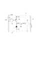
撮像装置は、図1に示すように、画素領域10と、垂直走査回路20と、水平走査回路30と、出力回路40と、制御回路50と、を含む。画素領域10には、複数行及び複数列にわたってマトリクス状に配された複数の光電変換素子11が設けられている。なお、光電変換素子11のすべての構成が複数行及び複数列に配される必要はない。少なくとも光電変換素子11に含まれるアバランシェダイオードが複数行及び複数列に配されていればよい。 As shown in FIG. 1, the image pickup apparatus includes a
画素領域10の各行には、第1の方向(図1において横方向)に延在して、制御線12が配されている。制御線12は、第1の方向に並ぶ複数の光電変換素子11のそれぞれに接続され、これら光電変換素子11に共通の信号線をなしている。制御線12の延在する第1の方向は、行方向或いは水平方向と表記することがある。制御線12の各々は、複数種類の制御信号を光電変換素子11に供給するための複数の信号線を含み得る。 A
また、画素領域10には、第1の方向に延在して、光電変換素子11に含まれる選択手段に接続された制御線VSELが配されている。図1および図2では、各光電変換素子11が選択手段を含むため、各行に制御線VSELが配されている。これに限らず、選択手段が複数の光電変換素子により共有される場合は、制御線VSELは選択手段が配された光電変換素子11に対応して配されていればよい。 Further, in the
画素領域10の各列には、第1の方向と交差する第2の方向(図1において縦方向)に延在して、データ線13が配されている。データ線13は、第2の方向に並ぶ複数の光電変換素子11のそれぞれに接続され、これら光電変換素子11に共通の信号線をなしている。データ線13の延在する第2の方向は、列方向或いは垂直方向と表記することがある。データ線13の各々は、光電変換素子11から出力されるデジタル信号をビット毎に転送するための複数の信号線を含み得る。 In each row of the
また、画素領域10には、第2の方向に延在して、光電変換素子11に含まれる選択手段に接続されたHSELが配される。図1および図2では、各光電変換素子11が選択手段を含むため、各列に制御線HSELが配されている。これに限らず、選択手段が複数の光電変換素子により共有される場合は、制御線HSELは選択手段が配された光電変換素子11に対応して配されていればよい。 Further, in the
各行の制御線12および制御線VSELは、垂直走査回路20に接続されている。垂直走査回路20は、光電変換素子11からの信号を読み出すための制御信号を、制御線12を介して光電変換素子11に供給する回路部である。 The
制御線12は、例えば、光電変換素子11に含まれる信号処理回路SPを制御する制御線である。垂直走査回路20は、画素領域10内の光電変換素子11を行単位で順次走査し、データ線13を介して各光電変換素子11の信号を出力回路40へと出力する。また、制御線VSELは、光電変換素子11に含まれる選択手段を制御する線である。 The
各列のデータ線13は、水平走査回路30に接続されている。各列の制御線HSELは、水平走査回路30に接続されている。水平走査回路30は、画素領域10から行単位で出力される各列の光電変換素子11の信号を選択して出力回路40へと順次出力する回路部である。水平走査回路30は、画素領域10の複数の列に対応する複数の保持部を備え、画素領域10から行単位で出力される各列の光電変換素子11の信号を対応する列の保持部にて保持する。水平走査回路30は、各列の保持部を順次走査し、各列の保持部に保持されている光電変換素子からの信号を順次出力回路40へと出力する。 The
出力回路40は、トランスミッタ回路41を有し、水平走査回路30から出力される、光電変換素子11からの信号を撮像装置の外部へと出力する回路部である。トランスミッタ回路41は、例えば、SerDes(SERializer/DESerializer)送信回路により構成されうる。SerDes送信回路は、例えば、LVDS(Low Voltage Differential Signaling)回路、SLVS(Scalable Low Voltage Signaling)回路である。なお、出力回路40を構成する外部インターフェース回路は、特に限定されるものではない。 The
制御回路50は、垂直走査回路20及び水平走査回路30の動作やそのタイミングを制御する制御信号を供給するための回路部である。なお、垂直走査回路20及び水平走査回路30の動作やそのタイミングを制御する制御信号の少なくとも一部は、撮像装置の外部から供給してもよい。 The
各々の光電変換素子11は、図2に示すように、アバランシェダイオードDと、クエンチ素子Rqと、波形整形部INVと、カウンタを含む信号処理回路SPと、を有する。アバランシェダイオードDは、光子の入射により生成される電荷をアバランシェ降伏により増倍するフォトダイオードにより構成され得る。このようなフォトダイオードは、具体的には、APD(Avalanche Photo Diode)やSPAD(Single Photon Avalanche Diode)である。SPADは、ブレークダウン電圧よりも高いバイアス電圧で動作させるガイガーモードでアバランシェ増倍を生じさせる。APDは、ブレークダウン電圧近傍の少し高いバイアス電圧で動作させるリニアモードでアバランシェ増倍を生じさせる。以下では、SPADを例にして説明する。アバランシェダイオードDと信号処理回路SPに含まれるカウンタとが接続されており、カウンタはアバランシェダイオードDに入射する光子に基づく信号をカウントする。クエンチ素子Rqは、例えばP型MOSトランジスタにより構成されうる。波形整形部INVは、例えばインバータ回路により構成されうる。波形整形部INVは、カウンタに接続されている。 As shown in FIG. 2, each
アバランシェダイオードDを構成するフォトダイオードのアノードには電圧Vssが供給され、カソードにはクエンチ素子Rqの一端と、波形整形部INVの入力端子が接続される。クエンチ素子Rqの他端には電圧Vddが供給される。波形整形部INVの出力端子は、信号処理回路SPのカウンタの入力端子に接続されている。信号処理回路SPの出力端子は、データ線13に接続されている。 A voltage Vss is supplied to the anode of the photodiode constituting the avalanche diode D, and one end of the quenching element Rq and the input terminal of the waveform shaping unit INV are connected to the cathode. A voltage Vdd is supplied to the other end of the quench element Rq. The output terminal of the waveform shaping unit INV is connected to the input terminal of the counter of the signal processing circuit SP. The output terminal of the signal processing circuit SP is connected to the
電圧Vss及び電圧Vddは、アバランシェダイオードDにガイガーモードで動作するに十分な逆バイアス電圧を印加することが可能なように設定されている。一例では、電圧Vssとして負の高電圧が与えられ、電圧Vddとして電源電圧程度の正電圧が与えられる。本実施形態では、アバランシェダイオードDを構成するフォトダイオードは、ガイガーモードで動作可能な単一光子アバランシェダイオード(SPAD)として使用する。本明細書では、アバランシェ増倍可能な逆バイアス電圧が印加されている状態をアクティブ状態ともいい、アバランシェ増倍可能な逆バイアス電圧が印加されていない状態を非アクティブ状態ともいう。 The voltage Vss and voltage Vdd are set so that a reverse bias voltage sufficient to operate in Geiger mode can be applied to the avalanche diode D. In one example, a negative high voltage is given as the voltage Vss, and a positive voltage of about the power supply voltage is given as the voltage Vdd. In this embodiment, the photodiode constituting the avalanche diode D is used as a single photon avalanche diode (SPAD) capable of operating in Geiger mode. In the present specification, a state in which a reverse bias voltage capable of multiplying the avalanche is applied is also referred to as an active state, and a state in which a reverse bias voltage capable of multiplying the avalanche is not applied is also referred to as an inactive state.
アバランシェダイオードDは、電圧Vddと電圧Vssとの間の電位差に相当する逆バイアス電圧が印加された状態となっている。この逆バイアス電圧は、アバランシェダイオードDの降伏電圧よりも高い電圧であり、アバランシェ増倍を起こすのに十分な電圧である(ガイガーモード)。しかし、アバランシェダイオードDに光子が入射していない状態では種となるキャリアが存在しないため、アバランシェ増倍は起こらず、アバランシェダイオードDに電流は流れない(待機状態)。 The avalanche diode D is in a state in which a reverse bias voltage corresponding to a potential difference between the voltage Vdd and the voltage Vss is applied. This reverse bias voltage is higher than the yield voltage of the avalanche diode D, and is a voltage sufficient to cause an avalanche multiplication (Geiger mode). However, since there is no seed carrier in the state where the photon is not incident on the avalanche diode D, the avalanche multiplication does not occur and no current flows through the avalanche diode D (standby state).
待機状態のアバランシェダイオードDに光子が入射すると、入射した光子により励起されてアバランシェダイオードD内にキャリアが生成される。アバランシェダイオードD内に生成されたキャリアは、アバランシェダイオードD内の高電界で加速されてアバランシェ増倍を引き起こし、大きななだれ電流が発生する(ガイガーモード動作)。このなだれ電流がクエンチ素子Rqを流れる。この電流による電圧降下により、アバランシェダイオードDのカソードの電位が下がり、アバランシェダイオードDの端子間の電位差が小さくなる。これにより、アバランシェダイオードDはガイガーモードから外れ(非ガイガーモード)、アバランシェ増倍が停止する。アバランシェダイオードDのカソード側のキャリアは、負荷として接続されたクエンチ素子Rqを介して徐々に排出される。つまり、アバランシェダイオードDのカソードには、クエンチ素子Rqを介して電位Vddが供給されるため、アバランシェダイオードDのカソードに供給される電位が電位Vddに戻る。これにより、アバランシェダイオードDの端子間の電位差は再び初期電圧に戻る。つまり、アバランシェダイオードDは再びガイガーモード又は待機状態に戻る。 When a photon is incident on the avalanche diode D in the standby state, it is excited by the incident photon and a carrier is generated in the avalanche diode D. The carriers generated in the avalanche diode D are accelerated by the high electric field in the avalanche diode D to cause avalanche multiplication, and a large avalanche current is generated (Geiger mode operation). This avalanche current flows through the quenching element Rq. Due to the voltage drop due to this current, the potential of the cathode of the avalanche diode D is lowered, and the potential difference between the terminals of the avalanche diode D is reduced. As a result, the avalanche diode D is released from the Geiger mode (non-Geiger mode), and the avalanche multiplication is stopped. The carrier on the cathode side of the avalanche diode D is gradually discharged via the quenching element Rq connected as a load. That is, since the potential Vdd is supplied to the cathode of the avalanche diode D via the quenching element Rq, the potential supplied to the cathode of the avalanche diode D returns to the potential Vdd. As a result, the potential difference between the terminals of the avalanche diode D returns to the initial voltage again. That is, the avalanche diode D returns to the Geiger mode or the standby state again.
この一連の動作について、図3を用いて説明する。図3は、本実施形態による撮像装置の駆動方法を示すタイミングチャートである。図3のタイミングチャートには、アバランシェダイオードDに光子が入射するタイミング、波形整形部INVに入力される信号Sig_Aを示している。また、図3のタイミングチャートには、信号Sig_Aの波形をパルス状の信号に整形し信号処理回路SPへと出力される信号Sig_D、信号処理回路SPによる信号Sig_Dの計数値(DOUT)を示している。 This series of operations will be described with reference to FIG. FIG. 3 is a timing chart showing a driving method of the image pickup apparatus according to the present embodiment. The timing chart of FIG. 3 shows the timing at which a photon is incident on the avalanche diode D and the signal Sigma_A input to the waveform shaping unit INV. Further, the timing chart of FIG. 3 shows the signal Sigma_D that shapes the waveform of the signal Sigma_A into a pulsed signal and outputs it to the signal processing circuit SP, and the count value (DOUT) of the signal Sigma_D by the signal processing circuit SP. There is.
初期状態において、アバランシェダイオードDに光子は入射しておらず、信号Sig_Aは待機状態を示す所定の電位であり、信号Sig_Dはローレベルである。また、信号処理回路SPの計数値は0である。 In the initial state, no photon is incident on the avalanche diode D, the signal Sigma_A is a predetermined potential indicating a standby state, and the signal Sigma_D is at a low level. Further, the count value of the signal processing circuit SP is 0.
アバランシェダイオードDに光子が入射すると、入射した光子により励起されたキャリアを種としてアバランシェ増倍が起こり、なだれ電流が流れることによって信号Sig_Aの電位は低下する。信号Sig_Aが所定の閾値以下になると、信号Sig_Dの電位はローレベルからハイレベルへと遷移する。 When a photon is incident on the avalanche diode D, the avalanche multiplication occurs by using the carrier excited by the incident photon as a seed, and the potential of the signal Sigma_A decreases due to the flow of the avalanche current. When the signal Sigma_A becomes equal to or less than a predetermined threshold value, the potential of the signal Sigma_D transitions from a low level to a high level.
その後、信号Sig_Aの電位は、クエンチ素子Rqを介して徐々に増加する。信号Sig_Aが所定の閾値を超えると、信号Sig_Dの電位はハイレベルからローレベルへと遷移する。 After that, the potential of the signal Sig_A gradually increases via the quenching element Rq. When the signal Sigma_A exceeds a predetermined threshold, the potential of the signal Sigma_D transitions from a high level to a low level.
信号処理回路SPに含まれるカウンタは、信号Sig_Dのパルス数に応じて計数値を1増加する。 The counter included in the signal processing circuit SP increments the count value by 1 according to the number of pulses of the signal Sigma_D.
上述の通り、波形整形部INVは、アバランシェ増倍により生起するアバランシェ電流の有無に基づいてパルスを発生する。そして、信号処理回路SPに含まれるカウンタは、アバランシェ電流の有無に基づくパルスの数をカウントする。信号処理回路SPは、カウント動作だけではなく、信号Sig_Dに対して所定の信号処理を行ってもよい。 As described above, the waveform shaping unit INV generates a pulse based on the presence or absence of the avalanche current generated by the avalanche multiplication. Then, the counter included in the signal processing circuit SP counts the number of pulses based on the presence or absence of the avalanche current. The signal processing circuit SP may perform predetermined signal processing on the signal Sigma_D as well as the counting operation.
信号処理回路SPは、垂直走査回路20から出力される制御信号12と後述する選択手段14からの制御信号とに応じて、信号処理後の信号である出力信号DOUTをデータ線13に出力する。 The signal processing circuit SP outputs an output signal DOUT, which is a signal after signal processing, to the
本実施形態は、選択手段14が信号処理回路SPから信号を出力するか否かを切り替えている。選択手段14を介して、制御線12、HSEL、VSELが信号処理回路SPに入力される。制御線12、HSEL、VSELが全てアクティブの場合に信号処理回路SPからの信号を読み出し、少なくともいずれかが非アクティブの場合には、信号処理回路SPからの信号を読み出さない。選択手段14は図2に示すようにAND回路などの組み合わせ回路で実現できるが、実現の方法はこれに限定しない。 In this embodiment, whether or not the selection means 14 outputs a signal from the signal processing circuit SP is switched. The control lines 12, HSEL, and VSEL are input to the signal processing circuit SP via the selection means 14. When the
本実施形態においても、所望の領域からのみ信号を読み出すことが可能となる。 Also in this embodiment, it is possible to read a signal only from a desired region.
図2では、信号処理回路SPのアクティブ・非アクティブを切り替えている。具体的には、信号処理回路SPとデータ線13との間のノードにスイッチを配置し、信号処理回路SPからデータ線への信号の読み出しを制御している。本明細書において、信号処理回路SPのアクティブとは、信号処理回路SPから信号が読み出される状態であることを指す。また、信号処理回路SPの非アクティブとは、信号処理回路SPから信号が読み出されない状態であることを指す。 In FIG. 2, the signal processing circuit SP is switched between active and inactive. Specifically, a switch is arranged at a node between the signal processing circuit SP and the
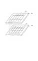
図4は、画素領域10の読み出し領域10aと非読み出し領域10bとのイメージを示す図である。図4において、光電変換素子(第1光電変換素子)からの信号を読み出す領域10aと、光電変換素子(第2光電変換素子)からの信号を読み出さない領域10bと、が示されている。図4に示す領域10bは、常に信号が出力されなくともよいし、第1のモードでは信号が出力されず、第1のモードが設定されている期間とは異なる期間に設定される第2のモードでは信号が出力されてもよい。 FIG. 4 is a diagram showing an image of a
本実施形態において、領域10aおよび領域10bにおいて光電変換が行われている。つまり、領域10bにも光が照射されている。本実施形態では、領域10bにおいても光電変換は行われているが、領域10bは信号の読出し速度向上等の観点から、読み出さないようにしている。つまり、不良画素ではないが、モードに応じて信号を読み出すか否かを制御している。ここで、モードとは、例えば、垂直走査回路20が画素領域10aに配された複数の光電変換素子を垂直走査する期間を指す。図2において、第1垂直走査で上から下に走査し終わるまでの期間は第1垂直走査の期間となる。上から下に走査し終わり下から上に戻った後、次に上から下に走査する期間は、第2垂直走査となる。図4(a)を用いて説明する。この説明では、第1のモードおよび第2のモードのそれぞれが、領域10aから信号を読み出すものとする。第1垂直走査期間とは、領域10aの上端に位置する光電変換素子を走査してから領域10aの下端に位置する光電変換素子を走査し終わるまでの期間を指す。そして第2垂直走査は、領域10aの上端に位置する光電変換素子を走査してから領域10aの下端に位置する光電変換素子を走査し終わるまでの期間を指す。本実施形態では、行または列方向に配されたすべての光電変換素子について読み出しを行わない場合は垂直または水平走査も行わない。これにより、すべての光電変換素子から信号を読み出す場合に比べて、信号の読出し時間を短くすることができる。 In this embodiment, photoelectric conversion is performed in the
例えば図4(a)では、画素領域10のうちm×n画素(m、nは自然数)の領域の信号のみを読み出す間引き読み出しを行う。図4(b)乃至図4(d)に示すように領域10aと領域10bとを制御することができる。図4(b)は、行間引き読み出しの例である。具体的には、所定の複数行に配された光電変換素子からの信号を読み出し、それ以外の行に配された光電変換素子からの信号を読み出さないようにしている。図4(c)は、列間引き読み出しの例である。具体的には、所定の複数列に配された光電変換素子からの信号を読み出し、それ以外の列に配された光電変換素子からの信号を読み出さないようにしている。図4(d)は、行列間引き読み出しの例である。具体的には、所定の位置に配された光電変換素子からの信号を読み出し、行及び列で信号を読み出さないようにしている。図4(a)乃至図4(d)に示すような行列単位でなく、画素単位で間引きを行ってもよい。例えば、図6に示すように、選択手段14がメモリMEMを含み、メモリMEMを用いることにより図4(e)に示すようにROI(Region Of Interest)読み出しを行うことができる。具体的には、信号線WRITEを介して各光電変換素子に含まれるメモリMEMに読み出しを行うか否かの信号が書き込まれる。この信号に基づいてスイッチをオンする電位を供給するかオフする電位を供給するかを制御してもよい。このように、設計者は本発明の効果を得るために様々な構成で選択手段14を実現してよい。 For example, in FIG. 4A, thinning out reading is performed to read only the signal in the area of m × n pixels (m and n are natural numbers) in the
第1のモードと第2のモードとは信号を読み出す領域10aが異なっていてもよい。例えば、まず、第1のモードでは、図4(a)〜図4(d)に示す領域10aに配された光電変換素子から信号を読み出す。そして、第2のモードでは、図4(a)〜図4(d)の領域10bに配された光電変換素子から信号を読み出し、領域10aに配された光電変換素子から信号を読み出すことも可能である。また、第1のモードでは、領域10aから信号を読み出し、領域10bから信号を読み出さず、第2のモードでは、領域10aおよび領域10bの両方から信号を読み出してもよい。つまり、第2のモードでは、信号が読み出されない状態に制御されていた光電変換素子を選択手段(第2選択手段)により信号が読み出さる状態に制御する。そして、信号が読み出される状態に制御されていた光電変換素子は信号が読み出される状態になるように維持されている。このような読み出し方法は、例えば、撮像装置が撮像を行う領域に不審者などの対象物が写るまでは第1のモードで撮像を行い、撮像を行う領域に対象物が写ると第1のモードから第2のモードに変える場合に有効である。対象物が写るまでは信号の読出し速度を重視し、対象物が写った後は画質を重視している。上述のとおり、撮像を行う目的に応じてモードを切り替えることが可能である。 The
また、図4(e)に示すROIでは、移動体を撮像する場合に、移動体の位置に応じて信号を読み出すか否かを切り替えることが可能となる。具体的には、撮像を行う領域のうちの第1部分に移動体が位置する第1のモードにおいては、第1部分のみ読み出しを行い、第1部分とは異なる第2部分に移動体が位置する第2のモードにおいては、第2部分のみ読み出しを行う。 Further, in the ROI shown in FIG. 4 (e), when an image of a moving body is taken, it is possible to switch whether or not to read a signal according to the position of the moving body. Specifically, in the first mode in which the moving body is located in the first part of the region to be imaged, only the first part is read out and the moving body is positioned in the second part different from the first part. In the second mode, only the second part is read.
図2では、選択手段14が信号処理回路SPに接続されているが、波形整形部INVの入力部や、波形整形部INVと信号処理回路SPとの間のノードに接続されていてもよい。この場合であっても、信号処理回路SPに含まれるカウンタにおいてカウントが行われなくなり、光電変換素子からの信号を出力しないようにすることができる。 In FIG. 2, although the selection means 14 is connected to the signal processing circuit SP, it may be connected to the input unit of the waveform shaping unit INV or the node between the waveform shaping unit INV and the signal processing circuit SP. Even in this case, the counter included in the signal processing circuit SP does not count, and the signal from the photoelectric conversion element can be prevented from being output.
本実施形態では、領域10aに含まれる光電変換素子は信号処理回路SPがアクティブとなるよう制御されるため、信号処理回路SPから信号が出力される。そして、領域10bに含まれる光電変換素子は、信号処理回路SPが非アクティブとなるよう制御されるため、信号処理回路SPから信号が出力されない。このように、本実施形態によれば、読み出しが不要な領域10bに属する光電変換素子11を選択することができる。これにより、撮像装置として信号の読み出し速度を、全光電変換素子を読み出す場合に比べて短くすることができる。 In the present embodiment, the photoelectric conversion element included in the
(第2実施形態)
図5を参照しながら第2実施形態に係る光電変換素子11について説明する。第2実施形態に係る光電変換素子11は、選択手段14がクエンチ素子Rqに接続されている点が第1実施形態とは異なる。以下で説明する事項以外は、第1実施形態と同様である。(Second Embodiment)
The
本実施形態において、クエンチ素子RqはMOSトランジスタで構成され、クエンチ素子Rqのゲート端子には、クエンチ素子Rqのオンオフを制御する選択手段14の出力端子が接続されている。選択手段14は、行ごとに配された制御線VSELと、列ごとに配された制御線HSELとが入力される。本実施形態では、信号VSELと信号HSELとによりクエンチ素子Rqのオンオフを制御することで、アバランシェダイオードDのアクティブ・非アクティブを切り替えている。信号VSELと信号HSELの両方がアクティブのとき、選択手段14はアバランシェダイオードDがアクティブとなるようクエンチ素子Rqを制御する。つまり、アバランシェダイオードDでアバランシェ増倍が生じ得る逆バイアス電圧が印加されるように選択手段14を制御する。図5では、クエンチ素子RqがPMOSトランジスタにより構成されるため、PMOSトランジスタのゲート端子に例えばグラウンド電圧を印加する。また、信号VSELと信号HSELの少なくとも一方が非アクティブのとき、選択手段14はアバランシェダイオードDが非非アクティブとなるようクエンチ素子Rqを制御する。つまり、アバランシェダイオードDでアバランシェ増倍が生じない電位となるように制御する。図4では、ゲート端子に例えばVddよりも高い電位を印加してPMOSトランジスタをオフ状態にする。これにより、カソードVddに電位が供給されなくなるため、アバランシェダイオードDでアバランシェ増倍が生じなくなる。 In the present embodiment, the quench element Rq is composed of a MOS transistor, and the output terminal of the selection means 14 for controlling the on / off of the quench element Rq is connected to the gate terminal of the quench element Rq. In the selection means 14, the control line VSEL arranged for each row and the control line HSEL arranged for each column are input. In the present embodiment, the active / inactive of the avalanche diode D is switched by controlling the on / off of the quenching element Rq by the signal VSEL and the signal HSEL. When both the signal VSEL and the signal HSEL are active, the selection means 14 controls the quenching element Rq so that the avalanche diode D becomes active. That is, the selection means 14 is controlled so that the avalanche diode D is applied with a reverse bias voltage that can cause an avalanche multiplication. In FIG. 5, since the quenching element Rq is composed of a epitaxial transistor, for example, a ground voltage is applied to the gate terminal of the epitaxial transistor. Further, when at least one of the signal VSEL and the signal HSEL is inactive, the selection means 14 controls the quenching element Rq so that the avalanche diode D becomes inactive. That is, the avalanche diode D is controlled so as to have a potential at which the avalanche multiplication does not occur. In FIG. 4, a potential higher than, for example, Vdd is applied to the gate terminal to turn off the epitaxial transistor. As a result, the potential is not supplied to the cathode Vdd, so that the avalanche diode D does not multiply the avalanche.
アバランシェダイオードDがアクティブの場合、光子が入射する度にアバランシェ電流が流れ、アバランシェダイオードDが非アクティブの場合、光子が入射してもアバランシェ電流は発生しない。したがって、アバランシェダイオードDが非アクティブの場合は、信号処理回路SPのカウンタで信号をカウントすることができず、光電変換素子11から信号が読み出されない。 When the avalanche diode D is active, an avalanche current flows each time a photon is incident, and when the avalanche diode D is inactive, an avalanche current is not generated even if a photon is incident. Therefore, when the avalanche diode D is inactive, the signal cannot be counted by the counter of the signal processing circuit SP, and the signal is not read from the
図5に示す選択回路14の代わりに、図6に示す選択回路14を用いてもよい。この場合は、信号線WRITEが必要になるため第1実施形態に比べて信号線が増える。このように、選択手段14が組み合わせ回路とメモリMEMとにより構成され、メモリMEMに入力される信号に基づいてアバランシェダイオードDのアクティブ・非アクティブを制御してもよい。 Instead of the
本実施形態では、領域10bに位置する光電変換素子の走査を行ってもよい。走査を行ったとしても、アバランシェ電流が生じていないため、カウンタの値は0となるためである。なお、領域10bに位置する光電変換素子のうち行または列方向に位置するすべての光電変換素子が信号を読み出さない光電変換素子である場合は、垂直または水平走査を行わないことが好ましい。つまり、間引いて走査を行うことが好ましい。これにより、信号の読出し速度を向上することができる。 In the present embodiment, the photoelectric conversion element located in the
画素領域10のすべての光電変換素子のアバランシェダイオードDがアクティブであると、すべての光電変換素子で光子が入射する度にアバランシェ電流が流れカウントが行われる。つまり、読み出したくない領域10bに属する光電変換素子11では無駄な消費電力が発生する。一方で、本実施形態によれば、領域10bに属する光電変換素子11のアバランシェダイオードDが非アクティブであるため、光子が入射してもアバランシェ電流は発生せず、カウントも行われない。領域10bに属する光電変換素子11には無駄な消費電力が発生せず、すべての光電変換素子からの信号を読み出す場合に比べて消費電力を低減できる。つまり、本実施形態によれば、第1実施形態で説明した効果に加えて、撮像装置を低消費電力とすることができる。また、垂直走査を行わない場合は、信号の読出し速度も向上させることができる。 When the avalanche diodes D of all the photoelectric conversion elements in the
(第3実施形態)
図7を参照しながら、第3実施形態の光電変換素子11について説明する。(Third Embodiment)
The
本実施形態は、アバランシェダイオードDのアノード又はクエンチ素子RqのアバランシェダイオードDが接続されたノードとは異なるノードに切替手段15が接続されている。そして、選択手段14は切替手段15を制御する点で第2実施形態と異なる。以下で説明する事項以外は第2実施形態と同様である。 In this embodiment, the switching means 15 is connected to a node different from the node to which the anode of the avalanche diode D or the avalanche diode D of the quenching element Rq is connected. The selection means 14 is different from the second embodiment in that the switching means 15 is controlled. The same applies to the second embodiment except for the matters described below.
図7においては、信号VSELと信号HSELの両方がアクティブのとき、選択手段14はクエンチ素子Rqが電圧Vddと接続されるように切替手段15を制御し、このときアバランシェダイオードDがアクティブとなる。また信号VSELと信号HSELの少なくとも一方が非アクティブのとき、選択手段14はクエンチ素子Rqが電圧VLと接続されるように切替手段15を制御し、このときアバランシェダイオードDが非アクティブとなる。このとき電圧VLは、アバランシェダイオードDがアバランシェ増倍を起こさない程度の任意の電圧に設定されている。 In FIG. 7, when both the signal VSEL and the signal HSEL are active, the selection means 14 controls the switching means 15 so that the quenching element Rq is connected to the voltage Vdd, and at this time, the avalanche diode D becomes active. Further, when at least one of the signal VSEL and the signal HSEL is inactive, the selection means 14 controls the switching means 15 so that the quenching element Rq is connected to the voltage VL, and at this time, the avalanche diode D becomes inactive. At this time, the voltage VL is set to an arbitrary voltage so that the avalanche diode D does not cause the avalanche multiplication.
同様にして、図8では、アバランシェダイオードDのアノードに切替手段15を設けている。アバランシェダイオードDがアクティブとなるよう制御するときにはアノードが電圧Vssと接続される。また、アバランシェダイオードDが非アクティブとなるよう制御するときには、アノードが電圧VHと接続される。このとき電圧VHは、アバランシェダイオードDがアバランシェ増幅を起こさない程度の任意の電圧に設定されている。 Similarly, in FIG. 8, the switching means 15 is provided at the anode of the avalanche diode D. When controlling the avalanche diode D to be active, the anode is connected to the voltage Vss. Also, when controlling the avalanche diode D to be inactive, the anode is connected to the voltage VH. At this time, the voltage VH is set to an arbitrary voltage so that the avalanche diode D does not cause avalanche amplification.
このように、本実施形態では、選択手段14を介して切替手段15が、アバランシェダイオードDに接続される電圧線を、アバランシェダイオードDがアクティブとなる電位が供給される電圧線か、非アクティブとなる電位が供給される電圧線VLか、で選択している。これにより、アバランェダイオードDのアクティブ・非アクティブを制御している。 As described above, in the present embodiment, the switching means 15 determines that the voltage line connected to the avalanche diode D via the selection means 14 is a voltage line to which a potential for activating the avalanche diode D is supplied or is inactive. The voltage line VL to which the potential is supplied is selected. Thereby, the active / inactive of the avalanche diode D is controlled.
本実施形態によれば、第1実施形態に比べて電圧線VL又は電圧線VHが増えるものの、第1実施形態と同様に所望の領域からのみ信号を読み出すことが可能となる。また、第1実施形態と同様に、アバランシェダイオードDのアクティブ・非アクティブを制御するため、撮像装置を低消費電力とすることができる。 According to the present embodiment, although the voltage line VL or the voltage line VH increases as compared with the first embodiment, it is possible to read the signal only from a desired region as in the first embodiment. Further, since the active / inactive of the avalanche diode D is controlled as in the first embodiment, the power consumption of the image pickup apparatus can be reduced.
(第4実施形態)
図9を参照しながら第4実施形態に係る撮像装置について説明する。図9は、第4実施形態に係る撮像装置の構造を示す概略図である。本実施形態における撮像装置は、第1の基板60bと、第2の基板60aとが積層されて成る。第1の基板60bは信号処理回路SPを有する光電変換素子セル(以下「セル」という)11dを複数有する。第2の基板60aはアバランシェダイオードDを有するセル11cを複数有する。セル11cとセル11dが各々接続される。すなわち、1つのセル11cと1つのセル11dが接続され、1つの光電変換素子11を構成する。(Fourth Embodiment)
The image pickup apparatus according to the fourth embodiment will be described with reference to FIG. FIG. 9 is a schematic view showing the structure of the image pickup apparatus according to the fourth embodiment. The image pickup apparatus in this embodiment is formed by laminating a
ここで、クエンチ素子Rqと、選択手段14と、波形整形部INVとは、セル11cとセル11dのいずれに配置されてもよい。例えば以下のような配置ができ、それぞれに特有の効果が期待できるため、設計者は目的に応じて様々な配置位置を採用できる。 Here, the quench element Rq, the selection means 14, and the waveform shaping unit INV may be arranged in either the
(配置例1)
セル11cにはアバランシェダイオードDのみを配置し、他の構成要素をすべてセル11dに配置することができる。この場合、アバランシェダイオードDの面積が最大となるため、光電変換素子11の開口率を高くできる。さらに、第2の基板60bはアバランシェダイオードDに特化したプロセスにできるため、画素特性も良好にできる。(Arrangement example 1)
Only the avalanche diode D can be arranged in the
(配置例2)
光電変換素子の構成要素に耐圧の異なるトランジスタが含まれる場合は、セル11dに低耐圧の構成要素のみを配置することができる。(Arrangement example 2)
When the components of the photoelectric conversion element include transistors having different withstand voltage, only the components with low withstand voltage can be arranged in the
例えばクエンチ素子Rqが高耐圧のトランジスタで構成され、その他のトランジスタが低耐圧のトランジスタで構成される場合、セル11cにはアバランシェダイオードDとクエンチ素子Rqを配置し、セル11dにはそれ以外のトランジスタを配置する。あるいは、高耐圧のトランジスタで構成されたクエンチ素子Rqに対し、選択手段14の出力段も高耐圧のトランジスタで構成される場合、セル11cにはアバランシェダイオードDと、クエンチ素子Rqと、選択手段14の出力段を配置する。このように、セル11dを低耐圧のトランジスタのみで構成できる。したがって、第1の基板60bの集積度を高くでき、また第1の基板60aを低耐圧のトランジスタに特化したプロセスにできるため、良好な回路特性を得られる。 For example, when the quench element Rq is composed of a transistor having a high withstand voltage and the other transistors are composed of a transistor having a low withstand voltage, the avalanche diode D and the quench element Rq are arranged in the
本実施形態におけるセル11cとセル11dへの光電変換素子11の各構成要素の配置について、前述の例に限らず、あらゆる配置をとることができる。 The arrangement of each component of the
本実施形態によれば、第1実施形態乃至第3実施形態で説明した効果に加えて、画素特性の低下を抑制しながら、撮像装置のチップサイズを小さくすることができる。 According to the present embodiment, in addition to the effects described in the first to third embodiments, the chip size of the image pickup apparatus can be reduced while suppressing the deterioration of the pixel characteristics.
(第5実施形態)
図10は、本実施形態に係る撮像システム200の構成を示すブロック図である。本実施形態の撮像システム200は、撮像装置204を含む。ここで、撮像装置204は、上述の実施形態で述べた撮像装置のいずれかを適用することができる。撮像システムの具体例としては、デジタルスチルカメラ、デジタルカムコーダー、監視カメラ等が挙げられる。図10では、撮像システム200としてデジタルスチルカメラの例を示している。(Fifth Embodiment)
FIG. 10 is a block diagram showing the configuration of the
図10に示す撮像システム200は、撮像装置204、被写体の光学像を撮像装置204に結像させるレンズ202、レンズ202を通過する光量を可変にするための絞り203、レンズ202の保護のためのバリア201を有する。レンズ202および絞り203は、撮像装置204に光を集光する光学系である。 The
撮像システム200は、撮像装置204から出力される出力信号の処理を行う信号処理部205を有する。信号処理部205は、必要に応じて入力信号に対して各種の補正、圧縮を行って出力する信号処理の動作を行う。撮像システム200は、更に、画像データを一時的に記憶するためのバッファメモリ部206、外部コンピュータ等と通信するための外部インターフェース部(外部I/F部)209を有する。更に撮像システム200は、撮像データの記録又は読み出しを行うための半導体メモリ等の記録媒体211、記録媒体211に記録または読み出しを行うための記録媒体制御インターフェース部(記録媒体制御I/F部)210を有する。記録媒体211は、撮像システム200に内蔵されていてもよく、着脱可能であってもよい。また、記録媒体制御I/F部210から記録媒体211との通信や外部I/F部209からの通信は無線によってなされてもよい。 The
更に撮像システム200は、各種演算を行うとともにデジタルスチルカメラ全体を制御する全体制御・演算部208、撮像装置204と信号処理部205に各種タイミング信号を出力するタイミング発生部207を有する。ここで、タイミング信号などは外部から入力されてもよく、撮像システム200は、少なくとも撮像装置204と、撮像装置204から出力された出力信号を処理する信号処理部205とを有すればよい。前述のように、制御回路50が垂直走査回路及び水平走査回路のすべての動作やそのタイミングを制御してもよいし、少なくとも一部がタイミング発生部207から供給されていてもよい。全体制御・演算部208およびタイミング発生部207は、撮像装置204の制御機能の一部または全部を実施するように構成してもよい。 Further, the
撮像装置204は、画像用信号を信号処理部205に出力する。信号処理部205は、撮像装置204から出力される画像用信号に対して所定の信号処理を実施し、画像データを出力する。また、信号処理部205は、画像用信号を用いて、画像を生成する。また、信号処理部205は、撮像装置204から出力される信号に対して測距演算を行ってもよい。なお、信号処理部205やタイミング発生部207は、撮像装置に搭載されていてもよい。信号処理部205やタイミング発生部207は、光電変換素子が配された基板に設けられていてもよく、第4実施形態に記載したような別の基板に設けられていてもよい。上述した各実施形態の撮像装置を用いて撮像システムを構成することにより、より良質の画像が取得可能な撮像システムを実現することができる。 The
(第6実施形態)
本実施形態の撮像システム及び移動体について、図11及び図12を用いて説明する。図11は、本実施形態による撮像システム及び移動体の構成例を示す概略図である。図12は、本実施形態による撮像システムの動作を示すフロー図である。本実施形態では、撮像システムとして、車載カメラの一例を示す。(Sixth Embodiment)
The imaging system and the moving body of the present embodiment will be described with reference to FIGS. 11 and 12. FIG. 11 is a schematic view showing a configuration example of an imaging system and a moving body according to the present embodiment. FIG. 12 is a flow chart showing the operation of the imaging system according to the present embodiment. In this embodiment, an example of an in-vehicle camera is shown as an imaging system.
図11は、車両システムとこれに搭載される撮像システムの一例を示したものである。撮像システム1301は、撮像装置1302、画像前処理部1315、集積回路1303、光学系1314を含む。光学系1314は、撮像装置1302に被写体の光学像を結像する。撮像装置1302は、光学系1314により結像された被写体の光学像を電気信号に変換する。撮像装置1302は、上述の各実施形態のいずれかの撮像装置である。画像前処理部1315は、撮像装置1302から出力された信号に対して所定の信号処理を行う。画像前処理部1315の機能は、撮像装置1302内に組み込まれていてもよい。撮像システム1301には、光学系1314、撮像装置1302及び画像前処理部1315が、少なくとも2組設けられており、各組の画像前処理部1315からの出力が集積回路1303に入力されるようになっている。 FIG. 11 shows an example of a vehicle system and an imaging system mounted on the vehicle system. The
集積回路1303は、撮像システム用途向けの集積回路であり、メモリ1305を含む画像処理部1304、光学測距部1306、視差演算部1307、物体認知部1308、異常検出部1309を含む。画像処理部1304は、画像前処理部1315の出力信号に対して、現像処理や欠陥補正等の画像処理を行う。メモリ1305は、撮像画像の一次記憶、撮像画素の欠陥位置を格納する。光学測距部1306は、被写体の合焦や、測距を行う。視差演算部1307は、複数の撮像装置1302により取得された複数の画像データから視差情報(視差画像の位相差)の算出を行う。物体認知部1308は、車、道、標識、人等の被写体の認知を行う。異常検出部1309は、撮像装置1302の異常を検出すると、主制御部1313に異常を発報する。 The
集積回路1303は、専用に設計されたハードウェアによって実現されてもよいし、ソフトウェアモジュールによって実現されてもよいし、これらの組合せによって実現されてもよい。また、FPGA(Field Programmable Gate Array)やASIC(Application Specific Integrated Circuit)等によって実現されてもよいし、これらの組合せによって実現されてもよい。 The
主制御部1313は、撮像システム1301、車両センサ1310、制御ユニット1320等の動作を統括・制御する。主制御部1313を持たず、撮像システム1301、車両センサ1310、制御ユニット1320が個別に通信インターフェースを有して、それぞれが通信ネットワークを介して制御信号の送受を行う(例えばCAN規格)方法も取り得る。 The
集積回路1303は、主制御部1313からの制御信号を受け或いは自身の制御部によって、撮像装置1302へ制御信号や設定値を送信する機能を有する。 The
撮像システム1301は、車両センサ1310に接続されており、車速、ヨーレート、舵角などの自車両走行状態及び自車外環境や他車・障害物の状態を検出することができる。車両センサ1310は、視差画像から対象物までの測距情報を取得する距離情報取得手段でもある。また、撮像システム1301は、自動操舵、自動巡行、衝突防止機能等の種々の運転支援を行う運転支援制御部1311に接続されている。特に、衝突判定機能に関しては、撮像システム1301や車両センサ1310の検出結果を基に他車・障害物との衝突推定・衝突有無を判定する。これにより、衝突が推定される場合の回避制御、衝突時の安全装置起動を行う。 The
また、撮像システム1301は、衝突判定部での判定結果に基づいて、ドライバーに警報を発する警報装置1312にも接続されている。例えば、衝突判定部の判定結果として衝突可能性が高い場合、主制御部1313は、ブレーキをかける、アクセルを戻す、エンジン出力を抑制するなどして、衝突を回避、被害を軽減する車両制御を行う。警報装置1312は、音等の警報を鳴らす、カーナビゲーションシステムやメーターパネルなどの表示部画面に警報情報を表示する、シートベルトやステアリングに振動を与えるなどしてユーザに警告を行う。 The
本実施形態では、車両の周囲、例えば前方又は後方を撮像システム1301で撮影する。図12(b)に、車両前方を撮像システム1301で撮像する場合の配置例を示す。 In the present embodiment, the surroundings of the vehicle, for example, the front or the rear, are photographed by the
2つの撮像装置1302は、車両1300の前方に配置される。具体的には、車両1300の進退方位又は外形(例えば車幅)に対する中心線を対称軸に見立て、その対称軸に対して2つの撮像装置1302が線対称に配置されると、車両1300と被写対象物との間の距離情報の取得や衝突可能性の判定を行う上で好ましい。また、撮像装置1302は、運転者が運転席から車両1300の外の状況を視認する際に運転者の視野を妨げない配置が好ましい。警報装置1312は、運転者の視野に入りやすい配置が好ましい。 The two
次に、撮像システム1301における撮像装置1302の故障検出動作について、図12を用いて説明する。撮像装置1302の故障検出動作は、図12に示すステップS1410〜S1480に従って実施される。 Next, the failure detection operation of the
ステップS1410は、撮像装置1302のスタートアップ時の設定を行うステップである。すなわち、撮像システム1301の外部(例えば主制御部1313)又は撮像システム1301の内部から、撮像装置1302の動作のための設定を送信し、撮像装置1302の撮像動作及び故障検出動作を開始する。 Step S1410 is a step of setting the
次いで、ステップS1420において、有効画素から画素信号を取得する。また、ステップS1430において、故障検出用に設けた故障検出画素からの出力値を取得する。この故障検出画素は、有効画素と同じく光電変換部として機能するアバランシェダイオードを備える。この光電変換部には、所定の電圧が書き込まれる。故障検出用画素は、この光電変換部に書き込まれた電圧に対応する信号を出力する。なお、ステップS1420とステップS1430とは逆でもよい。 Next, in step S1420, a pixel signal is acquired from the effective pixel. Further, in step S1430, the output value from the failure detection pixel provided for failure detection is acquired. The failure detection pixel includes an avalanche diode that functions as a photoelectric conversion unit like the effective pixel. A predetermined voltage is written in this photoelectric conversion unit. The failure detection pixel outputs a signal corresponding to the voltage written in the photoelectric conversion unit. The steps S1420 and S1430 may be reversed.
次いで、ステップS1440において、故障検出画素の出力期待値と、実際の故障検出画素からの出力値との該非判定を行う。ステップS1440における該非判定の結果、出力期待値と実際の出力値とが一致している場合は、ステップS1450に移行し、撮像動作が正常に行われていると判定し、処理ステップがステップS1460へと移行する。ステップS1460では、走査行の画素信号をメモリ1305に送信して一次保存する。そののち、ステップS1420に戻り、故障検出動作を継続する。一方、ステップS1440における該非判定の結果、出力期待値と実際の出力値とが一致していない場合は、処理ステップはステップS1470に移行する。ステップS1470において、撮像動作に異常があると判定し、主制御部1313、又は警報装置1312に警報を発報する。警報装置1312は、表示部に異常が検出されたことを表示させる。その後、ステップS1480において撮像装置1302を停止し、撮像システム1301の動作を終了する。 Next, in step S1440, the non-determination of the expected output value of the failure detection pixel and the output value from the actual failure detection pixel is performed. If the expected output value and the actual output value match as a result of the non-determination in step S1440, the process proceeds to step S1450, it is determined that the imaging operation is normally performed, and the processing step proceeds to step S1460. And migrate. In step S1460, the pixel signal of the scanning line is transmitted to the
なお、本実施形態では、1行毎にフローチャートをループさせる例を例示したが、複数行毎にフローチャートをループさせてもよいし、1フレーム毎に故障検出動作を行ってもよい。ステップS1470の警報の発報は、無線ネットワークを介して、車両の外部に通知するようにしてもよい。 In the present embodiment, an example in which the flowchart is looped for each line is illustrated, but the flowchart may be looped for each of a plurality of lines, or the failure detection operation may be performed for each frame. The alarm issued in step S1470 may be notified to the outside of the vehicle via the wireless network.
また、本実施形態では、他の車両と衝突しない制御を説明したが、他の車両に追従して自動運転する制御や、車線からはみ出さないように自動運転する制御などにも適用可能である。さらに、撮像システム1301は、自車両等の車両に限らず、例えば、船舶、航空機或いは産業用ロボットなどの移動体(移動装置)に適用することができる。加えて、移動体に限らず、高度道路交通システム(ITS)等、広く物体認識を利用する機器に適用することができる。 Further, in the present embodiment, the control that does not collide with another vehicle has been described, but it can also be applied to a control that automatically drives following another vehicle, a control that automatically drives so as not to go out of the lane, and the like. .. Further, the
本発明の撮像装置は、更に、カラーフィルタやマイクロレンズを有する構成であってもよく、距離情報など各種情報を取得可能な構成であってもよい。 The imaging device of the present invention may further have a configuration including a color filter and a microlens, and may have a configuration capable of acquiring various information such as distance information.
本発明は、上記実施形態に限らず種々の変形が可能である。例えば、いずれかの実施形態の一部の構成を他の実施形態に追加した例や、他の実施形態の一部の構成と置換した例も、本発明の実施形態である。例えば、第1実施形態のようにアバランシェダイオードDのアクティブ・非アクティブを制御しながら信号処理回路SPからの信号を出力するか否かを制御してもよい。また、上述の実施形態は、いずれも本発明を実施するにあたっての具体化の例を示したものに過ぎず、これらの例示によって本発明の技術的範囲が限定的に解釈されてはならない。すなわち、本発明はその技術思想、又はその主要な特徴から逸脱することなく、様々な態様で実施することができる。 The present invention is not limited to the above embodiment and can be modified in various ways. For example, an example in which a part of the configuration of any of the embodiments is added to another embodiment or an example in which a part of the configuration of another embodiment is replaced with another embodiment is also an embodiment of the present invention. For example, as in the first embodiment, it may be possible to control whether or not to output a signal from the signal processing circuit SP while controlling the active / inactive of the avalanche diode D. In addition, all of the above-described embodiments merely show examples of embodiment in carrying out the present invention, and the technical scope of the present invention should not be construed in a limited manner by these examples. That is, the present invention can be implemented in various aspects without departing from the technical idea or its main features.
10 画素領域
11 光電変換素子
14 選択手段
15 切替手段
D アバランシェダイオード
Vdd 電圧
Vss 電圧
VH 電圧
VL 電圧10
Claims (20)
Translated fromJapanese前記複数の光電変換素子のうちの第1光電変換素子に対応して第1選択手段が設けられ、
前記複数の光電変換素子のうちの第2光電変換素子に対応して第2選択手段が設けられ、
第1のモードにおいて、前記第1選択手段により前記第1光電変換素子からの信号が読み出される状態に制御され、前記第2選択手段により前記第2光電変換素子からの信号が読み出されない状態に制御され、
前記第1のモードが設定されている期間とは異なる期間に設定される第2のモードにおいて、前記信号が読み出されない状態に制御されていた前記第2光電変換素子を前記第2選択手段により信号が読み出される状態に制御することを特徴とする撮像装置。A plurality of photoelectric conversion elements including an avalanche diode and a counter for counting a signal based on light incident on the avalanche diode are provided.
A first selection means is provided corresponding to the first photoelectric conversion element among the plurality of photoelectric conversion elements.
A second selection means is provided corresponding to the second photoelectric conversion element among the plurality of photoelectric conversion elements.
In the first mode, the first selection means controls the signal from the first photoelectric conversion element to be read, and the second selection means does not read the signal from the second photoelectric conversion element. Controlled
In the second mode set to a period different from the period in which the first mode is set, the second photoelectric conversion element controlled so that the signal is not read is subjected to the second selection means. An imaging device characterized in that it controls a state in which a signal is read out.
前記第1のモードは、第1垂直走査が行われている期間であり、
前記第2のモードは、第2垂直走査が行われている期間であることを特徴とする請求項1乃至3のいずれか1項に記載の撮像装置。At least a part of the plurality of photoelectric conversion elements is arranged side by side in the first direction.
The first mode is a period during which the first vertical scan is performed.
The imaging device according to any one of claims 1 to 3, wherein the second mode is a period during which the second vertical scanning is performed.
前記垂直走査回路と前記水平走査回路とにより前記第1選択手段および前記第2選択手段を制御することを特徴とする請求項1乃至4のいずれか1項に記載の撮像装置。Equipped with a vertical scanning circuit and a horizontal scanning circuit,
The imaging apparatus according to any one of claims 1 to 4, wherein the first selection means and the second selection means are controlled by the vertical scanning circuit and the horizontal scanning circuit.
前記第1選択手段は、前記第1光電変換素子の前記クエンチ素子のオンオフを制御していることを特徴とする請求項1乃至5のいずれか1項に記載の撮像装置。Each of the plurality of photoelectric conversion elements includes a quenching element connected to the avalanche diode.
The imaging device according to any one of claims 1 to 5, wherein the first selection means controls on / off of the quench element of the first photoelectric conversion element.
前記制御線は、前記アバランシェダイオードがアバランシェ増倍を起こさない状態となる電位を供給する第1電圧線と、前記アバランシェダイオードがアバランシェ増倍可能な状態となる電位を供給する第2電圧線と、を備え、
前記第1選択手段および前記第2選択手段は、前記アバランシェダイオードに接続する制御線を前記第1電圧線および前記第2電圧線で選択することを特徴とする請求項1乃至5のいずれか1項に記載の撮像装置。Each of the plurality of photoelectric conversion elements is connected to a control line that controls a potential applied to the anode or cathode of the avalanche diode.
The control lines include a first voltage line that supplies a potential that causes the avalanche diode to not cause avalanche multiplication, and a second voltage line that supplies a potential that allows the avalanche diode to become avalanche multiplyable. With
Any one of claims 1 to 5, wherein the first selection means and the second selection means select a control line connected to the avalanche diode with the first voltage line and the second voltage line. The imaging apparatus according to the section.
前記第1のモードから前記第2のモードに変わることを特徴とする請求項14に記載の撮像装置。When an object is captured in the area to be imaged by the imaging device,
The imaging device according to claim 14, wherein the first mode is changed to the second mode.
前記第1基板は、前記カウンタを含み、
前記第2基板は、前記アバランシェダイオードを含むことを特徴とする請求項1乃至15のいずれか1項に記載の撮像装置。A first substrate and a second substrate laminated on the first substrate are provided.
The first substrate includes the counter.
The imaging device according to any one of claims 1 to 15, wherein the second substrate includes the avalanche diode.
前記第2基板は、前記波形整形部を含むことを特徴とする請求項16に記載の撮像装置。The photoelectric conversion element includes a waveform shaping unit and includes a waveform shaping unit.
The imaging device according to claim 16, wherein the second substrate includes the waveform shaping unit.
前記第2基板は、前記クエンチ素子を含むことを特徴とする請求項17に記載の撮像装置。The photoelectric conversion element includes a quenching element.
The imaging device according to claim 17, wherein the second substrate includes the quenching element.
前記撮像装置が出力する信号を処理する信号処理部と、を有することを特徴とする撮像システム。The imaging device according to any one of claims 1 to 18.
An imaging system including a signal processing unit that processes a signal output by the imaging apparatus.
前記撮像装置からの信号に基づく情報から、対象物までの距離情報を取得する距離情報取得手段と、を有する移動体であって、
前記距離情報に基づいて前記移動体を制御する制御手段をさらに有することを特徴とする移動体。The imaging device according to any one of claims 1 to 18.
A moving body having a distance information acquisition means for acquiring distance information to an object from information based on a signal from the image pickup apparatus.
A moving body further comprising a control means for controlling the moving body based on the distance information.
Priority Applications (3)
| Application Number | Priority Date | Filing Date | Title |
|---|---|---|---|
| JP2019210035AJP2021082973A (en) | 2019-11-20 | 2019-11-20 | Imaging device, imaging system, and moving object |
| US17/099,622US11695022B2 (en) | 2019-11-20 | 2020-11-16 | Image capturing apparatus, image capturing system, and moving body |
| JP2024161922AJP2024169589A (en) | 2019-11-20 | 2024-09-19 | Imaging device, imaging system, and mobile object |
Applications Claiming Priority (1)
| Application Number | Priority Date | Filing Date | Title |
|---|---|---|---|
| JP2019210035AJP2021082973A (en) | 2019-11-20 | 2019-11-20 | Imaging device, imaging system, and moving object |
Related Child Applications (1)
| Application Number | Title | Priority Date | Filing Date |
|---|---|---|---|
| JP2024161922ADivisionJP2024169589A (en) | 2019-11-20 | 2024-09-19 | Imaging device, imaging system, and mobile object |
Publications (2)
| Publication Number | Publication Date |
|---|---|
| JP2021082973Atrue JP2021082973A (en) | 2021-05-27 |
| JP2021082973A5 JP2021082973A5 (en) | 2022-11-15 |
Family
ID=75910067
Family Applications (2)
| Application Number | Title | Priority Date | Filing Date |
|---|---|---|---|
| JP2019210035APendingJP2021082973A (en) | 2019-11-20 | 2019-11-20 | Imaging device, imaging system, and moving object |
| JP2024161922APendingJP2024169589A (en) | 2019-11-20 | 2024-09-19 | Imaging device, imaging system, and mobile object |
Family Applications After (1)
| Application Number | Title | Priority Date | Filing Date |
|---|---|---|---|
| JP2024161922APendingJP2024169589A (en) | 2019-11-20 | 2024-09-19 | Imaging device, imaging system, and mobile object |
Country Status (2)
| Country | Link |
|---|---|
| US (1) | US11695022B2 (en) |
| JP (2) | JP2021082973A (en) |
Cited By (5)
| Publication number | Priority date | Publication date | Assignee | Title |
|---|---|---|---|---|
| JPWO2021117632A1 (en)* | 2019-12-13 | 2021-06-17 | ||
| WO2022019189A1 (en)* | 2020-07-22 | 2022-01-27 | 浜松ホトニクス株式会社 | Photodetection device |
| JP2023061644A (en)* | 2021-10-20 | 2023-05-02 | キヤノン株式会社 | Photoelectric conversion device |
| WO2023131996A1 (en)* | 2022-01-05 | 2023-07-13 | キヤノン株式会社 | Photoelectric conversion device and light detection system |
| WO2024004516A1 (en)* | 2022-06-29 | 2024-01-04 | キヤノン株式会社 | Photoelectric conversion device and photoelectric conversion system |
Families Citing this family (1)
| Publication number | Priority date | Publication date | Assignee | Title |
|---|---|---|---|---|
| CN116740799A (en)* | 2022-03-02 | 2023-09-12 | 安徽省东超科技有限公司 | Optical recognition device and three-dimensional image acquisition method |
Citations (10)
| Publication number | Priority date | Publication date | Assignee | Title |
|---|---|---|---|---|
| US7057147B1 (en)* | 2003-12-17 | 2006-06-06 | Itt Manufacturing Enterprises Inc. | Imaging system and method for collecting energy from at least two sensing elements adjacent one another between rows of sensing elements |
| JP2008228232A (en)* | 2007-03-15 | 2008-09-25 | Canon Inc | Imaging apparatus, imaging method, program, and storage medium |
| WO2009031287A1 (en)* | 2007-09-07 | 2009-03-12 | Panasonic Corporation | Multi-color image processing apparatus and signal processing apparatus |
| JP2013529035A (en)* | 2010-06-01 | 2013-07-11 | 博立▲碼▼杰通▲訊▼(深▲せん▼)有限公司 | Multispectral photosensitive element and sampling method thereof |
| JP2018198388A (en)* | 2017-05-24 | 2018-12-13 | キヤノン株式会社 | Solid-state image sensor, imaging apparatus, and imaging method |
| WO2019035369A1 (en)* | 2017-08-15 | 2019-02-21 | ソニーセミコンダクタソリューションズ株式会社 | Solid-state imaging device and drive method thereof |
| JP2019100919A (en)* | 2017-12-05 | 2019-06-24 | シャープ株式会社 | Light reception element, time-of-flight measurement device, and optical radar device |
| JP2019140525A (en)* | 2018-02-09 | 2019-08-22 | キヤノン株式会社 | Photoelectric conversion device and imaging system |
| JP2019186925A (en)* | 2018-04-06 | 2019-10-24 | キヤノン株式会社 | Imaging device and imaging system |
| US20190324143A1 (en)* | 2018-04-20 | 2019-10-24 | Sick Ag | Optoelectronic sensor and method of distance determination |
Family Cites Families (13)
| Publication number | Priority date | Publication date | Assignee | Title |
|---|---|---|---|---|
| JP5521721B2 (en) | 2009-08-28 | 2014-06-18 | ソニー株式会社 | Image sensor and camera system |
| US9299732B2 (en) | 2013-10-28 | 2016-03-29 | Omnivision Technologies, Inc. | Stacked chip SPAD image sensor |
| LU92665B1 (en) | 2015-02-24 | 2016-08-25 | Leica Microsystems | METHOD FOR IMPROVING THE DYNAMIC RANGE OF A DEVICE FOR DETECTING LIGHT |
| US10014340B2 (en) | 2015-12-28 | 2018-07-03 | Taiwan Semiconductor Manufacturing Co., Ltd. | Stacked SPAD image sensor |
| JP7055544B2 (en) | 2016-11-29 | 2022-04-18 | ソニーセミコンダクタソリューションズ株式会社 | Sensor chips and electronic devices |
| JP6929671B2 (en) | 2017-03-17 | 2021-09-01 | キヤノン株式会社 | Imaging device and imaging system |
| US10312275B2 (en)* | 2017-04-25 | 2019-06-04 | Semiconductor Components Industries, Llc | Single-photon avalanche diode image sensor with photon counting and time-of-flight detection capabilities |
| JP6954086B2 (en) | 2017-12-19 | 2021-10-27 | セイコーエプソン株式会社 | Liquid containment |
| EP3503534B1 (en) | 2017-12-20 | 2021-08-18 | Canon Kabushiki Kaisha | Solid-state image sensor, image capturing apparatus, and image capturing method |
| JP2019140137A (en) | 2018-02-06 | 2019-08-22 | 株式会社豊田中央研究所 | Photodetector |
| US10996323B2 (en)* | 2018-02-22 | 2021-05-04 | Stmicroelectronics (Research & Development) Limited | Time-of-flight imaging device, system and method |
| JP7013925B2 (en)* | 2018-02-23 | 2022-02-01 | 株式会社デンソー | Optical ranging device and its method |
| US11644549B2 (en)* | 2019-03-06 | 2023-05-09 | The University Court Of The University Of Edinburgh | Extended dynamic range and reduced power imaging for LIDAR detector arrays |
- 2019
- 2019-11-20JPJP2019210035Apatent/JP2021082973A/enactivePending
- 2020
- 2020-11-16USUS17/099,622patent/US11695022B2/enactiveActive
- 2024
- 2024-09-19JPJP2024161922Apatent/JP2024169589A/enactivePending
Patent Citations (10)
| Publication number | Priority date | Publication date | Assignee | Title |
|---|---|---|---|---|
| US7057147B1 (en)* | 2003-12-17 | 2006-06-06 | Itt Manufacturing Enterprises Inc. | Imaging system and method for collecting energy from at least two sensing elements adjacent one another between rows of sensing elements |
| JP2008228232A (en)* | 2007-03-15 | 2008-09-25 | Canon Inc | Imaging apparatus, imaging method, program, and storage medium |
| WO2009031287A1 (en)* | 2007-09-07 | 2009-03-12 | Panasonic Corporation | Multi-color image processing apparatus and signal processing apparatus |
| JP2013529035A (en)* | 2010-06-01 | 2013-07-11 | 博立▲碼▼杰通▲訊▼(深▲せん▼)有限公司 | Multispectral photosensitive element and sampling method thereof |
| JP2018198388A (en)* | 2017-05-24 | 2018-12-13 | キヤノン株式会社 | Solid-state image sensor, imaging apparatus, and imaging method |
| WO2019035369A1 (en)* | 2017-08-15 | 2019-02-21 | ソニーセミコンダクタソリューションズ株式会社 | Solid-state imaging device and drive method thereof |
| JP2019100919A (en)* | 2017-12-05 | 2019-06-24 | シャープ株式会社 | Light reception element, time-of-flight measurement device, and optical radar device |
| JP2019140525A (en)* | 2018-02-09 | 2019-08-22 | キヤノン株式会社 | Photoelectric conversion device and imaging system |
| JP2019186925A (en)* | 2018-04-06 | 2019-10-24 | キヤノン株式会社 | Imaging device and imaging system |
| US20190324143A1 (en)* | 2018-04-20 | 2019-10-24 | Sick Ag | Optoelectronic sensor and method of distance determination |
Cited By (7)
| Publication number | Priority date | Publication date | Assignee | Title |
|---|---|---|---|---|
| JPWO2021117632A1 (en)* | 2019-12-13 | 2021-06-17 | ||
| JP7658581B2 (en) | 2019-12-13 | 2025-04-08 | 国立大学法人京都大学 | Quantum absorption spectroscopy system and quantum absorption spectroscopy method |
| WO2022019189A1 (en)* | 2020-07-22 | 2022-01-27 | 浜松ホトニクス株式会社 | Photodetection device |
| JP2023061644A (en)* | 2021-10-20 | 2023-05-02 | キヤノン株式会社 | Photoelectric conversion device |
| JP7543236B2 (en) | 2021-10-20 | 2024-09-02 | キヤノン株式会社 | Photoelectric conversion device |
| WO2023131996A1 (en)* | 2022-01-05 | 2023-07-13 | キヤノン株式会社 | Photoelectric conversion device and light detection system |
| WO2024004516A1 (en)* | 2022-06-29 | 2024-01-04 | キヤノン株式会社 | Photoelectric conversion device and photoelectric conversion system |
Also Published As
| Publication number | Publication date |
|---|---|
| US11695022B2 (en) | 2023-07-04 |
| US20210151481A1 (en) | 2021-05-20 |
| JP2024169589A (en) | 2024-12-05 |
Similar Documents
| Publication | Publication Date | Title |
|---|---|---|
| JP2021082973A (en) | Imaging device, imaging system, and moving object | |
| US11937004B2 (en) | Photoelectric conversion apparatus, imaging system, movable object, and semiconductor substrate | |
| US11069823B2 (en) | Photoelectric conversion device, photoelectric conversion system, and movable object comprising a comparison unit to compare the count value of pulse with a predetermined threshold value | |
| JP6924085B2 (en) | Photodetector and imaging system | |
| JP7089390B2 (en) | Photoelectric conversion device and its driving method | |
| JP7630985B2 (en) | Photoelectric conversion device and driving method thereof | |
| JP7379000B2 (en) | Photoelectric conversion devices, photoelectric conversion systems, and mobile objects | |
| JP2021027277A (en) | Photoelectric conversion device and photoelectric conversion system | |
| JP2024160505A (en) | Photoelectric conversion device, light detection system, movable body, and method of controlling photoelectric conversion device | |
| JP2020123846A (en) | Photoelectric conversion device, imaging system, moving body | |
| JP7422451B2 (en) | Photoelectric conversion devices, photoelectric conversion systems, and mobile objects | |
| JP2021034559A (en) | Photoelectric converters, photoelectric conversion systems, and mobiles | |
| JP2019165286A (en) | Photoelectric conversion device and imaging system | |
| US11240453B2 (en) | Photoelectric conversion device | |
| JP7639097B2 (en) | Photoelectric conversion device, photoelectric conversion system, and mobile body | |
| JP2019186401A (en) | Photodetection device, photodetection system, and mobile body | |
| JP7571188B2 (en) | Photoelectric conversion device and imaging system | |
| US20240381000A1 (en) | Photoelectric conversion apparatus, device, and moving body | |
| JP7718952B2 (en) | signal processing device | |
| US20250203238A1 (en) | Photoelectric conversion device | |
| US20230163229A1 (en) | Photoelectric conversion element and photoelectric conversion device | |
| US20250008237A1 (en) | Imaging system, movable apparatus, imaging method, and storage medium | |
| JP2024163733A (en) | Photoelectric conversion device and photoelectric conversion system | |
| WO2025204825A1 (en) | Photoelectric conversion device, imaging system, and mobile body | |
| JP2025149065A (en) | Photoelectric conversion device, imaging system, mobile object |
Legal Events
| Date | Code | Title | Description |
|---|---|---|---|
| A521 | Request for written amendment filed | Free format text:JAPANESE INTERMEDIATE CODE: A523 Effective date:20221107 | |
| A621 | Written request for application examination | Free format text:JAPANESE INTERMEDIATE CODE: A621 Effective date:20221107 | |
| A977 | Report on retrieval | Free format text:JAPANESE INTERMEDIATE CODE: A971007 Effective date:20230828 | |
| A131 | Notification of reasons for refusal | Free format text:JAPANESE INTERMEDIATE CODE: A131 Effective date:20230912 | |
| A521 | Request for written amendment filed | Free format text:JAPANESE INTERMEDIATE CODE: A523 Effective date:20231108 | |
| RD01 | Notification of change of attorney | Free format text:JAPANESE INTERMEDIATE CODE: A7421 Effective date:20231213 | |
| A131 | Notification of reasons for refusal | Free format text:JAPANESE INTERMEDIATE CODE: A131 Effective date:20240206 | |
| A521 | Request for written amendment filed | Free format text:JAPANESE INTERMEDIATE CODE: A523 Effective date:20240405 | |
| A02 | Decision of refusal | Free format text:JAPANESE INTERMEDIATE CODE: A02 Effective date:20240625 | |
| A521 | Request for written amendment filed | Free format text:JAPANESE INTERMEDIATE CODE: A523 Effective date:20240919 | |
| A911 | Transfer to examiner for re-examination before appeal (zenchi) | Free format text:JAPANESE INTERMEDIATE CODE: A911 Effective date:20240930 | |
| A912 | Re-examination (zenchi) completed and case transferred to appeal board | Free format text:JAPANESE INTERMEDIATE CODE: A912 Effective date:20241025 | |
| A521 | Request for written amendment filed | Free format text:JAPANESE INTERMEDIATE CODE: A523 Effective date:20250723 |