JP2021077451A - Plasma processing apparatus and plasma processing method - Google Patents
Plasma processing apparatus and plasma processing methodDownload PDFInfo
- Publication number
- JP2021077451A JP2021077451AJP2019200801AJP2019200801AJP2021077451AJP 2021077451 AJP2021077451 AJP 2021077451AJP 2019200801 AJP2019200801 AJP 2019200801AJP 2019200801 AJP2019200801 AJP 2019200801AJP 2021077451 AJP2021077451 AJP 2021077451A
- Authority
- JP
- Japan
- Prior art keywords
- antenna
- plasma processing
- electromagnetic wave
- space
- phase
- Prior art date
- Legal status (The legal status is an assumption and is not a legal conclusion. Google has not performed a legal analysis and makes no representation as to the accuracy of the status listed.)
- Withdrawn
Links
- 238000003672processing methodMethods0.000titleclaimsabstractdescription10
- 239000000758substrateSubstances0.000claimsabstractdescription25
- 239000002131composite materialSubstances0.000claimsdescription25
- 230000005684electric fieldEffects0.000claimsdescription16
- 238000000034methodMethods0.000claimsdescription5
- 230000002194synthesizing effectEffects0.000claimsdescription5
- 238000000638solvent extractionMethods0.000claimsdescription2
- 230000005855radiationEffects0.000description23
- 238000010586diagramMethods0.000description9
- 230000007246mechanismEffects0.000description7
- 230000005540biological transmissionEffects0.000description6
- 238000004891communicationMethods0.000description6
- 230000008878couplingEffects0.000description6
- 238000010168coupling processMethods0.000description6
- 238000005859coupling reactionMethods0.000description6
- 230000002093peripheral effectEffects0.000description6
- 239000004020conductorSubstances0.000description4
- 230000005404monopoleEffects0.000description4
- 238000009832plasma treatmentMethods0.000description4
- 239000004065semiconductorSubstances0.000description4
- 229910052782aluminiumInorganic materials0.000description3
- XAGFODPZIPBFFR-UHFFFAOYSA-NaluminiumChemical compound[Al]XAGFODPZIPBFFR-UHFFFAOYSA-N0.000description3
- 230000015572biosynthetic processEffects0.000description3
- 239000000919ceramicSubstances0.000description3
- 229910052751metalInorganic materials0.000description3
- 239000002184metalSubstances0.000description3
- 238000003786synthesis reactionMethods0.000description3
- PNEYBMLMFCGWSK-UHFFFAOYSA-Naluminium oxideInorganic materials[O-2].[O-2].[O-2].[Al+3].[Al+3]PNEYBMLMFCGWSK-UHFFFAOYSA-N0.000description2
- 239000012141concentrateSubstances0.000description2
- 230000005672electromagnetic fieldEffects0.000description2
- 239000011347resinSubstances0.000description2
- 229920005989resinPolymers0.000description2
- 238000004088simulationMethods0.000description2
- 229910001369BrassInorganic materials0.000description1
- RYGMFSIKBFXOCR-UHFFFAOYSA-NCopperChemical compound[Cu]RYGMFSIKBFXOCR-UHFFFAOYSA-N0.000description1
- YCKRFDGAMUMZLT-UHFFFAOYSA-NFluorine atomChemical compound[F]YCKRFDGAMUMZLT-UHFFFAOYSA-N0.000description1
- 239000004642PolyimideSubstances0.000description1
- 239000004809TeflonSubstances0.000description1
- 229920006362Teflon®Polymers0.000description1
- 230000003321amplificationEffects0.000description1
- 239000010951brassSubstances0.000description1
- 238000006243chemical reactionMethods0.000description1
- 229910052802copperInorganic materials0.000description1
- 239000010949copperSubstances0.000description1
- 229910052593corundumInorganic materials0.000description1
- 230000000694effectsEffects0.000description1
- 238000005530etchingMethods0.000description1
- 229910052731fluorineInorganic materials0.000description1
- 239000011737fluorineSubstances0.000description1
- 150000002500ionsChemical class0.000description1
- 239000000463materialSubstances0.000description1
- 239000007769metal materialSubstances0.000description1
- 238000003199nucleic acid amplification methodMethods0.000description1
- 230000010363phase shiftEffects0.000description1
- 229920001721polyimidePolymers0.000description1
- -1polytetrafluoroethylenePolymers0.000description1
- 229920001343polytetrafluoroethylenePolymers0.000description1
- 239000004810polytetrafluoroethyleneSubstances0.000description1
- 239000010453quartzSubstances0.000description1
- VYPSYNLAJGMNEJ-UHFFFAOYSA-Nsilicon dioxideInorganic materialsO=[Si]=OVYPSYNLAJGMNEJ-UHFFFAOYSA-N0.000description1
- 239000007787solidSubstances0.000description1
- 229910001220stainless steelInorganic materials0.000description1
- 239000010935stainless steelSubstances0.000description1
- 238000005728strengtheningMethods0.000description1
- 238000004804windingMethods0.000description1
- 229910001845yogo sapphireInorganic materials0.000description1
Images


Classifications
- H—ELECTRICITY
- H01—ELECTRIC ELEMENTS
- H01J—ELECTRIC DISCHARGE TUBES OR DISCHARGE LAMPS
- H01J37/00—Discharge tubes with provision for introducing objects or material to be exposed to the discharge, e.g. for the purpose of examination or processing thereof
- H01J37/32—Gas-filled discharge tubes
- H01J37/32009—Arrangements for generation of plasma specially adapted for examination or treatment of objects, e.g. plasma sources
- H01J37/32192—Microwave generated discharge
- H01J37/32211—Means for coupling power to the plasma
- H01J37/32238—Windows
- H—ELECTRICITY
- H01—ELECTRIC ELEMENTS
- H01J—ELECTRIC DISCHARGE TUBES OR DISCHARGE LAMPS
- H01J37/00—Discharge tubes with provision for introducing objects or material to be exposed to the discharge, e.g. for the purpose of examination or processing thereof
- H01J37/32—Gas-filled discharge tubes
- H01J37/32009—Arrangements for generation of plasma specially adapted for examination or treatment of objects, e.g. plasma sources
- H01J37/32082—Radio frequency generated discharge
- H01J37/321—Radio frequency generated discharge the radio frequency energy being inductively coupled to the plasma
- H01J37/3211—Antennas, e.g. particular shapes of coils
- H—ELECTRICITY
- H05—ELECTRIC TECHNIQUES NOT OTHERWISE PROVIDED FOR
- H05H—PLASMA TECHNIQUE; PRODUCTION OF ACCELERATED ELECTRICALLY-CHARGED PARTICLES OR OF NEUTRONS; PRODUCTION OR ACCELERATION OF NEUTRAL MOLECULAR OR ATOMIC BEAMS
- H05H1/00—Generating plasma; Handling plasma
- H05H1/24—Generating plasma
- H05H1/46—Generating plasma using applied electromagnetic fields, e.g. high frequency or microwave energy
- H—ELECTRICITY
- H01—ELECTRIC ELEMENTS
- H01J—ELECTRIC DISCHARGE TUBES OR DISCHARGE LAMPS
- H01J37/00—Discharge tubes with provision for introducing objects or material to be exposed to the discharge, e.g. for the purpose of examination or processing thereof
- H01J37/32—Gas-filled discharge tubes
- H01J37/32009—Arrangements for generation of plasma specially adapted for examination or treatment of objects, e.g. plasma sources
- H01J37/32082—Radio frequency generated discharge
- H01J37/321—Radio frequency generated discharge the radio frequency energy being inductively coupled to the plasma
- H01J37/32119—Windows
- H—ELECTRICITY
- H01—ELECTRIC ELEMENTS
- H01J—ELECTRIC DISCHARGE TUBES OR DISCHARGE LAMPS
- H01J37/00—Discharge tubes with provision for introducing objects or material to be exposed to the discharge, e.g. for the purpose of examination or processing thereof
- H01J37/32—Gas-filled discharge tubes
- H01J37/32009—Arrangements for generation of plasma specially adapted for examination or treatment of objects, e.g. plasma sources
- H01J37/32192—Microwave generated discharge
- H01J37/32211—Means for coupling power to the plasma
- H01J37/3222—Antennas
- H—ELECTRICITY
- H01—ELECTRIC ELEMENTS
- H01L—SEMICONDUCTOR DEVICES NOT COVERED BY CLASS H10
- H01L21/00—Processes or apparatus adapted for the manufacture or treatment of semiconductor or solid state devices or of parts thereof
- H01L21/02—Manufacture or treatment of semiconductor devices or of parts thereof
- H01L21/04—Manufacture or treatment of semiconductor devices or of parts thereof the devices having potential barriers, e.g. a PN junction, depletion layer or carrier concentration layer
- H01L21/18—Manufacture or treatment of semiconductor devices or of parts thereof the devices having potential barriers, e.g. a PN junction, depletion layer or carrier concentration layer the devices having semiconductor bodies comprising elements of Group IV of the Periodic Table or AIIIBV compounds with or without impurities, e.g. doping materials
- H01L21/30—Treatment of semiconductor bodies using processes or apparatus not provided for in groups H01L21/20 - H01L21/26
- H01L21/302—Treatment of semiconductor bodies using processes or apparatus not provided for in groups H01L21/20 - H01L21/26 to change their surface-physical characteristics or shape, e.g. etching, polishing, cutting
- H01L21/306—Chemical or electrical treatment, e.g. electrolytic etching
- H01L21/3065—Plasma etching; Reactive-ion etching
- H—ELECTRICITY
- H01—ELECTRIC ELEMENTS
- H01Q—ANTENNAS, i.e. RADIO AERIALS
- H01Q1/00—Details of, or arrangements associated with, antennas
- H01Q1/12—Supports; Mounting means
- H01Q1/22—Supports; Mounting means by structural association with other equipment or articles
- H01Q1/26—Supports; Mounting means by structural association with other equipment or articles with electric discharge tube
- H—ELECTRICITY
- H01—ELECTRIC ELEMENTS
- H01Q—ANTENNAS, i.e. RADIO AERIALS
- H01Q3/00—Arrangements for changing or varying the orientation or the shape of the directional pattern of the waves radiated from an antenna or antenna system
- H01Q3/26—Arrangements for changing or varying the orientation or the shape of the directional pattern of the waves radiated from an antenna or antenna system varying the relative phase or relative amplitude of energisation between two or more active radiating elements; varying the distribution of energy across a radiating aperture
- H01Q3/2605—Array of radiating elements provided with a feedback control over the element weights, e.g. adaptive arrays
- H01Q3/2611—Means for null steering; Adaptive interference nulling
- H01Q3/2617—Array of identical elements
Landscapes
- Physics & Mathematics (AREA)
- Engineering & Computer Science (AREA)
- Plasma & Fusion (AREA)
- Chemical & Material Sciences (AREA)
- Analytical Chemistry (AREA)
- Electromagnetism (AREA)
- Spectroscopy & Molecular Physics (AREA)
- General Physics & Mathematics (AREA)
- Condensed Matter Physics & Semiconductors (AREA)
- Manufacturing & Machinery (AREA)
- Computer Hardware Design (AREA)
- Microelectronics & Electronic Packaging (AREA)
- Power Engineering (AREA)
- Plasma Technology (AREA)
- Drying Of Semiconductors (AREA)
- Chemical Vapour Deposition (AREA)
Abstract
Description
Translated fromJapanese本開示は、プラズマ処理装置およびプラズマ処理方法に関する。 The present disclosure relates to a plasma processing apparatus and a plasma processing method.
電磁波のパワーによりガスをプラズマ化し、チャンバ内で半導体ウエハ等の基板にプラズマ処理を行うプラズマ処理装置が知られている。例えば、特許文献1には、チャンバの天壁を構成する誘電体部材と、マイクロ波(電磁波)を出力するマイクロ波出力部と、誘電体部材上に配置された複数のマイクロ波放射機構とを有するプラズマ処理装置が開示されている。特許文献1のプラズマ処理装置では、マイクロ波出力部から出力されたマイクロ波を、複数のマイクロ波放射部のアンテナから誘電体部材を介してチャンバ内に放射し、チャンバ内にプラズマを形成して基板に対してプラズマ処理を行う。 There is known a plasma processing apparatus that turns gas into plasma by the power of electromagnetic waves and performs plasma processing on a substrate such as a semiconductor wafer in a chamber. For example,
本開示は、複数のアンテナの配置によらず、自在にプラズマ分布制御を行うことができるプラズマ処理装置およびプラズマ処理方法を提供する。 The present disclosure provides a plasma processing apparatus and a plasma processing method capable of freely controlling a plasma distribution regardless of the arrangement of a plurality of antennas.
本開示の一態様に係るプラズマ処理装置は、基板にプラズマ処理を施す処理空間および電磁波を合成する合成空間を有するチャンバと、前記処理空間と前記合成空間とを仕切る誘電体窓と、前記合成空間に電磁波を放射する複数のアンテナを有し、フェーズドアレイアンテナとして機能するアンテナユニットと、前記アンテナユニットに電磁波を出力する電磁波出力部と、前記アンテナユニットをフェーズドアレイアンテナとして機能させる制御部と、を有し、前記アンテナはヘリカルアンテナである。 The plasma processing apparatus according to one aspect of the present disclosure includes a chamber having a processing space for applying plasma processing to a substrate and a synthetic space for synthesizing electromagnetic waves, a dielectric window for partitioning the processing space from the synthetic space, and the synthetic space. An antenna unit that has a plurality of antennas that radiate electromagnetic waves and functions as a phased array antenna, an electromagnetic wave output unit that outputs electromagnetic waves to the antenna unit, and a control unit that causes the antenna unit to function as a phased array antenna. The antenna is a helical antenna.
本開示によれば、複数の電磁波放射機構の配置によらず、自在にプラズマ分布制御を行うことができるプラズマ処理装置およびプラズマ処理方法が提供される。 According to the present disclosure, there is provided a plasma processing apparatus and a plasma processing method capable of freely controlling a plasma distribution regardless of the arrangement of a plurality of electromagnetic wave radiation mechanisms.
以下、添付図面を参照して実施形態について具体的に説明する。 Hereinafter, embodiments will be specifically described with reference to the accompanying drawings.
<プラズマ処理装置の構成>
図1は、一実施形態に係るプラズマ処理装置を示す断面図である。
本実施形態のプラズマ処理装置100は、電磁波(マイクロ波)によって表面波プラズマを形成し、形成された表面波プラズマにより基板Wに対して成膜処理やエッチング処理等のプラズマ処理を施すものである。基板Wとしては典型例として半導体ウエハを挙げることができるが、これに限らず、FPD基板やセラミックス基板等の他の基板であってよい。<Plasma processing equipment configuration>
FIG. 1 is a cross-sectional view showing a plasma processing apparatus according to an embodiment.
The
プラズマ処理装置100は、チャンバ1と、アンテナユニット2と、電磁波出力部3と、制御部4とを有する。 The
チャンバ1は、略円筒状をなし、上部が開放された容器部11と、容器部11の上部開口を閉塞する天板12とを有する。チャンバ1は、アルミニウム、ステンレス鋼等の金属材料で形成されている。 The
チャンバ1内の空間は、誘電体窓13で上下に仕切られており、誘電体窓13の上側の空間が電磁波を合成する合成空間14、下側の空間が基板Wに対してプラズマ処理を行う処理空間15となっている。誘電体窓13は、例えば、石英、アルミナ(Al2O3)等のセラミックス、ポリテトラフルオロエチレン等のフッ素系樹脂やポリイミド系樹脂により形成されている。合成空間14は大気空間であり、アンテナユニット2の後述する複数のアンテナから合成空間14に電磁波が放射され、合成される。また、処理空間15には基板Wを水平状態で載置する円板状をなすステージ21が設けられ、その中に基板Wを処理するための表面波プラズマが形成される。処理空間15は、プラズマ処理中には真空状態にされる。 The space inside the
ステージ21は、絶縁部材22を介して立設された筒状の支持部材23により支持されている。ステージ21を構成する材料としては、表面が陽極酸化処理されたアルミニウム等の金属やセラミックス等の誘電体部材が例示される。ステージ21には、基板Wを静電吸着するための静電チャック、温度制御機構、基板Wの裏面に熱伝達用のガスを供給するガス流路等が設けられてもよい。 The
また、プラズマ処理によっては、ステージ21に整合器を介して高周波バイアス電源が電気的に接続されてもよい。高周波バイアス電源からステージ21に高周波電力が供給されることにより、基板W側にプラズマ中のイオンが引き込まれる。 Further, depending on the plasma processing, a high frequency bias power supply may be electrically connected to the
チャンバ1の底部には排気管24が接続されており、排気管24には圧力制御バルブや真空ポンプを含む排気装置25が接続されている。排気装置25を作動させるとチャンバ1の処理空間15内が排気され、所定の真空度まで減圧される。チャンバ1の側壁には、基板Wの搬入および搬出を行うための搬入出口26と、搬入出口26を開閉するゲートバルブ27とが設けられている。 An
チャンバ1側壁の誘電体窓13下方位置には、内部にリング状のガス流路が形成され、当該ガス流路からその内側に開口する複数のガス吐出孔を有するシャワーリング28が設けられており、シャワーリング28にはガス供給機構29が接続されている。ガス供給機構29からは、プラズマ生成ガスとして用いられるArガスのような希ガス、およびプラズマ処理のための処理ガスが供給される。 At a position below the
アンテナユニット2は、電磁波出力部3から出力された電磁波をチャンバ1の上方からチャンバ1内の合成空間14に放射するものであり、複数のアンテナモジュール31を有している。アンテナモジュール31は、位相器32と、アンプ部33と、電磁波放射部34とを有する。電磁波放射部34は、アンプ部33で増幅した電磁波を伝送する伝送路35と、伝送路35から延び、合成空間14に電磁波を放射するアンテナ36を有する。アンテナ36はヘリカルアンテナである。アンテナモジュール31の位相器32とアンプ部33は、チャンバ1の上方に設けられている。 The antenna unit 2 radiates the electromagnetic wave output from the electromagnetic wave output unit 3 from above the
位相器32は、電磁波の位相を変化させるものであり、アンテナ36から放射される電磁波の位相を進めたり遅らせたりして位相を調整できるように構成されている。位相器32により電磁波の位相を調整することにより、電磁波の干渉を利用して誘電体窓13の所望の位置に電磁波を集中させることが可能である。 The
アンプ部33は、可変ゲインアンプ、ソリッドステートアンプを構成するメインアンプ、およびアイソレータを有している。可変ゲインアンプは、メインアンプへ入力する電磁波の電力レベルを調整し、個々のアンテナモジュール31のばらつきを調整または電磁波強度調整のためのアンプである。メインアンプは、例えば、入力整合回路と、半導体増幅素子と、出力整合回路と、高Q共振回路とを有する構成とすることができる。アイソレータは、アンテナ36で反射してメインアンプに向かう反射電磁波を分離するものである。 The
電磁波放射部34の伝送路35は天板12にはめ込まれており、伝送路35の下端が天板の内壁と同じ高さとなっている。アンテナ36は伝送路35の下端から、その軸が鉛直になるように合成空間14内へ延びている。すなわち、アンテナ36は、合成空間14の上壁の内面から合成空間14内に延びている。アンテナ36としては、銅や真鍮、または銀めっきされたアルミニウム等を用いることができる。アンテナ36を構成するヘリカルアンテナの詳細については後述する。 The
図2に示すように、伝送路35は、中心に配置された内側導体41と、その周囲に配置された外側導体42と、これらの間に設けられたテフロン(登録商標)等の誘電体部材43とを有し、同軸ケーブル状をなしている。符号44はスリーブである。アンテナ36は、内側導体41に接続されている。 As shown in FIG. 2, the
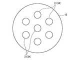
複数のアンテナモジュール31(電磁波放射部34)は天板12に対して均等に設けられる。アンテナモジュール31の数は、適切なプラズマが形成されるような適宜の数に設定される。本例では、図3に示すように、アンテナモジュール31(電磁波放射部34)は7つ設けられている(図1では3つのみ図示)。 A plurality of antenna modules 31 (electromagnetic wave emitting units 34) are evenly provided on the
各アンテナモジュール31の位相器32によりアンテナ36から放射される電磁波の位相を調整することにより、電磁波の干渉を生じさせ、誘電体窓13の任意の部分に電磁波を集中させることが可能となっている。すなわち、アンテナユニット2はフェーズドアレイアンテナとして機能する。 By adjusting the phase of the electromagnetic wave radiated from the
電磁波出力部3は、図4に示すように、電源51と、発振器52と、発振された電磁波を増幅するアンプ53と、増幅された電磁波を各アンテナモジュール31に分配する分配器54とを有しており、各アンテナモジュール31に電磁波を出力する。 As shown in FIG. 4, the electromagnetic wave output unit 3 includes a
発振器52は電磁波を例えばPLL発振させる。電磁波としては、例えば860MHzの周波数のものを用いる。電磁波の周波数としては、860MHzの他に、500MHzから3GHzの範囲の所望の周波数を用いることができる。分配器54は、アンプ53で増幅された電磁波を分配する。 The
制御部4は、CPUを有しており、プラズマ処理装置100における各構成部を制御する。制御部4は、プラズマ処理装置100の制御パラメータおよび処理レシピを記憶した記憶部や、入力手段、ディスプレイ等を備えている。制御部4は、電磁波出力部3のパワーやガス供給機構29からのガスの供給等を制御する。また、制御部4は、各アンテナモジュール31の位相器32に制御信号を出力し、各アンテナモジュール31の電磁波放射部34(アンテナ36)から放射される電磁波の位相を制御し、電磁波に干渉を生じさせて誘電体窓13の所望部分に電磁波を集光するように制御する。つまり、制御部4はアンテナユニット2をフェーズドアレイアンテナとして機能させるように制御する。 The control unit 4 has a CPU and controls each component in the
制御部4による位相器32の制御は、例えば、予め、記憶部に各アンテナモジュールの位相と電磁波の集光位置の関係を示すテーブルを複数記憶させておき、高速でテーブルを切り替えることにより行うことができる。 The control unit 4 controls the
なお、アンテナユニット2、電磁波出力部3、および制御部4は、プラズマ処理のためのプラズマを生成するプラズマ源を構成する。 The antenna unit 2, the electromagnetic wave output unit 3, and the control unit 4 form a plasma source that generates plasma for plasma processing.
[ヘリカルアンテナ]
次に、アンテナ36を構成するヘリカルアンテナについて説明する。
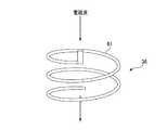
アンテナ36を構成するヘリカルアンテナは、図5の斜視図に示すように、金属線61をらせん状に巻いたアンテナであり、特定の範囲内の寸法でらせんの軸方向への指向性が高い性質を有する。このため、アンテナ36から放射される電磁波の放射成分は真下方向が主体となり、横方向への放射成分が少ないことから、アンテナ間の相互結合が少なく、壁での反射も小さい。[Helical antenna]
Next, the helical antenna constituting the
As shown in the perspective view of FIG. 5, the helical antenna constituting the
また、アンテナ36を構成するヘリカルアンテナの形状および配置を最適化することにより、電磁波の干渉をより生じやすくすることができ、また、電界分布制御の制御性を高くすることができる。 Further, by optimizing the shape and arrangement of the helical antennas constituting the
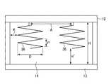
図6は、合成空間14に配置されるヘリカルアンテナに関するパラメータを説明する図である。図6では便宜上、ヘリカルアンテナを2つ配置した状態を示している。図中Dはヘリカルアンテナの直径、Pはヘリカルアンテナのピッチ、Aはアンテナ間の距離、Hは合成空間14の高さ、H´はヘリカルアンテナの下端から誘電体窓13までの高さ、Kはアンテナと合成空間14の側壁までの距離である。また、図6では、ヘリカルアンテナの巻き数Nを3として描いている。 FIG. 6 is a diagram illustrating parameters relating to the helical antenna arranged in the
ヘリカルアンテナでは、電磁波の波長をλとすると、ひと巻きでλになるように設計され、直径Dはλ/πとなる。ただし、微調整のための10〜20%の大小は許容される。アンテナ間の距離Aは、電磁波の干渉を生じさせるのに適した距離であって、かつ互いに物理的に干渉しない距離であることが必要であり、A≦λ/2であることが好ましい。 The helical antenna is designed so that it becomes λ in one turn, where λ is the wavelength of the electromagnetic wave, and the diameter D is λ / π. However, a size of 10 to 20% for fine adjustment is allowed. The distance A between the antennas needs to be a distance suitable for causing electromagnetic wave interference and a distance that does not physically interfere with each other, and A ≦ λ / 2 is preferable.
また、ヘリカルアンテナの典型的な形状については、Antennas
2nd edition by John D. Kraus (1988)に記載されている。この文献の284ページには、一般的なヘリカルアンテナについて、巻き数NがN>3と記載されており、また、ヘリカルアンテナのらせんの角度αが、12°<α<14°と記載されている。αからピッチPを計算すると、λ/5<P<λ/4となる。この条件は、電磁波ビームの幅が小さくなり、放射特性(直進性)が良好になる範囲である。For the typical shape of the helical antenna, see Antennas.
It is described in the 2nd edition by John D. Kraus (1988). On page 284 of this document, the number of turns N is described as N> 3 for a general helical antenna, and the spiral angle α of the helical antenna is described as 12 ° <α <14 °. There is. When the pitch P is calculated from α, λ / 5 <P <λ / 4. This condition is a range in which the width of the electromagnetic wave beam becomes small and the radiation characteristics (straightness) become good.
しかし、本実施形態では、複数のアンテナ36から放射する電磁波が干渉することが必要であるため、放射特性よりもアンテナ36の下方で電磁波の干渉が起こりやすい条件であることが好ましい。このような観点から、巻き数NおよびピッチPについては、一般的なヘリカルアンテナとは異なり、巻き数Nが1〜3、ピッチPがλ/12〜λ/8の範囲(特にλ/10程度が好ましい。)が選択される。 However, in the present embodiment, since it is necessary for the electromagnetic waves radiated from the plurality of
また、電磁波を合成する合成空間14は上壁と側壁とが金属で囲まれた閉鎖空間であり、合成空間の高さHが大きすぎると電磁波の多重反射により導波管モードが発生し、電界分布制御が困難となる。導波管モードには、TM01、TE01等の種々のパターンがあり、条件によっていずれかのパターンが現出する。また、高さHが小さすぎると電磁波の干渉が生じ難くなる。このため、合成空間14の高さHはλ/4〜λ/2の範囲が好ましい。また、合成空間14の高さHが上記範囲を満たしても、ヘリカルアンテナの下端から誘電体窓13までの高さH´が大きすぎると多重反射が生じ、小さすぎると電磁波の干渉が生じ難くなるため、高さH´を規定することがより重要である。このような点から、ヘリカルアンテナの下端から誘電体窓13の表面までの高さH´はλ/8〜λ/2の範囲が好ましい。また、上述したように、ヘリカルアンテナは、軸方向の指向性が高いため、合成空間14の側壁での反射は生じ難いが、アンテナと合成空間14の側壁までの距離Kがλ/10より小さくなると、側壁での反射の影響が生じる。このため、Kはλ/10以上が好ましい。 Further, the
電磁波の波長が860MHzの場合、λ=348.6mmであるから、各パラメータの好ましい範囲は以下のようになる。
直径D:88.8〜133.2mm((λ/π)±20%とした値)
距離A:174.3mm以下
ピッチP:29.1〜43.6mm(特に34.9mm程度)
高さH:87.2〜174.3mm
高さH´:43.6〜174.3mm
距離K:34.9mmWhen the wavelength of the electromagnetic wave is 860 MHz, λ = 348.6 mm, so the preferable range of each parameter is as follows.
Diameter D: 88.8 to 133.2 mm (value set to (λ / π) ± 20%)
Distance A: 174.3 mm or less Pitch P: 29.1-43.6 mm (especially about 34.9 mm)
Height H: 87.2 to 174.3 mm
Height H': 43.6 to 174.3 mm
Distance K: 34.9 mm
<プラズマ処理装置の動作>
次に、以上のように構成されるプラズマ処理装置100の動作について説明する。以下の動作は、制御部4による制御に基づいてなされる。<Operation of plasma processing device>
Next, the operation of the
最初に、ゲートバルブ27を開けてチャンバ1に隣接する真空搬送室から搬送装置(いずれも図示せず)により搬入出口26を介して基板Wを真空排気されたチャンバ1の処理空間15に搬入し、ステージ21上に載置する。 First, the
ゲートバルブ27を閉じた後、排気装置25により処理空間15を所定の真空圧力に調整し、ガス導入機構29から処理空間15内にプラズマ処理のためのガスを導入しつつ、電磁波出力部3から電磁波を出力する。電磁波出力部3から出力された電磁波は、アンテナユニット2の複数のアンテナモジュール31に供給され、複数のアンテナモジュール31の電磁波放射部34からチャンバ1の合成空間14に放射される。 After closing the
このとき、従来の複数の電磁波放射部を有するプラズマ処理装置と同様、位相制御を行わない図7のプラズマ処理装置200では、アンテナユニット2´の複数の電磁波放射部34(アンテナ36)から放射される電磁波Eの位相は同じである。このため、図7に示すように、電磁波Eの干渉は生じず、電磁波放射部34に対応する部分の電界強度が高く、電磁波放射部34の間の部分の電界強度が低くなる。すなわち、電界強度の分布は電磁波放射部34の物理的配置に依存し、したがって、プラズマ分布も電磁波放射部34の物理的配置に依存した強弱を有する不均一なものとなる。 At this time, in the
これに対し、本実施形態では、図8に示すように、制御部4から位相器32に制御信号を出力することにより、各アンテナモジュール31の電磁波放射部34(アンテナ36)から放射される電磁波Eの位相を制御する。すなわち、アンテナユニット2をフェーズドアレイアンテナとして機能させる。これにより、合成空間14で電磁波Eを合成する際に、電磁波の干渉を生じさせて、誘電体窓13の所望部分に電磁波Eが集光する部分、つまり電磁波強度が高い部分を形成することができ、その部分で局部的に電界強度を高めることができる。また、電磁波放射部34から放射される電磁波Eの位相制御により、電磁波の集光部分を高速で移動させることができる。 On the other hand, in the present embodiment, as shown in FIG. 8, the electromagnetic wave radiated from the electromagnetic wave radiating unit 34 (antenna 36) of each
誘電体窓13に集光された電磁波は、誘電体窓13を透過し、その電界によりガスがプラズマ化され、処理空間15における集光部分の直下位置にプラズマが集中して生成される。そして、位相制御により集光部分を高速で移動させることで、電磁波放射部34の物理的配置によらず、自在にプラズマ分布制御を行うことができる。 The electromagnetic wave focused on the
[位相制御の詳細]
次に、アンテナユニット2をフェーズアレイアンテナとして機能させる際の電磁波の位相制御の詳細について、図9〜図11を参照して説明する。[Details of phase control]
Next, the details of the phase control of the electromagnetic wave when the antenna unit 2 functions as the phase array antenna will be described with reference to FIGS. 9 to 11.
図9は、一実施形態に係るプラズマ処理装置100における集光原理を説明するための模式図である。電磁波放射部34からの電磁波放射位置が存在する天板12の裏面を放射面Rとし、電磁波が照射される誘電体窓13の表面を照射面Fとし、放射面Rと照射面Fとの距離をzとする。照射面Fにおける電磁波を集光させたい位置をOとし、位置Oと対応する放射面Rの位置をO´とする。このとき、位置O´からxだけ離れた電磁波放射部34から放射される電磁波の位相を考える。集光させたい位置Oと位置O´の距離はzであり、位置Oと電磁波放射部34の電磁波放射位置xの距離は、(x2+z2)1/2である。電磁波の波数をk(=2π/λ(ただし、λは電磁波の波長))とし、位置xから放射した電磁波の位置Oでの位相(すなわち、位置xから放射した電磁波の位置Oでの位相の、位置O´から放射した電磁波の位置Oでの位相に対する位相差)をδ(x)すると、以下の(1)式が成り立つ。
k(x2+z2)1/2−δ(x)=kz ・・・(1)
(1)式を変形すると、位相δ(x)を求める以下の(2)式が得られる。
δ(x)=k{(x2+z2)1/2−z} ・・・(2)
δ(x)をxの関数として座標上に表すと図10に示す曲線となる。FIG. 9 is a schematic diagram for explaining the focusing principle in the
k (x2 + z2 )1/2 −δ (x) = kz ・ ・ ・ (1)
By modifying the equation (1), the following equation (2) for obtaining the phase δ (x) can be obtained.
δ (x) = k {(x2 + z2 )1/2 −z} ・ ・ ・ (2)
When δ (x) is represented on the coordinates as a function of x, the curve shown in FIG. 10 is obtained.
位相δ(x)は、位置O´から位置Oに至る電磁波と位置xから位置Oに至る電磁波の進行方向のずれとして把握することができ、電磁波放射部34の電磁波放射位置が位置O´から離れるほど(すなわちxが大きくなるほど)大きくなる。このため、位相δ(x)の値に応じて、電磁波放射部34から放射される電磁波の位相θを早めたり遅らせたりすることにより、複数の電磁波放射部34から放射された電磁波を位置Oで強め合うようにすることができる。 The phase δ (x) can be grasped as a deviation in the traveling direction between the electromagnetic wave from the position O'to the position O and the electromagnetic wave from the position x to the position O, and the electromagnetic wave radiation position of the electromagnetic
例えば、図11に示すように、7つの電磁波放射部34a、34b、34c、34d、34e、34f、34gとし、電磁波放射部34bの電磁波放射位置が位置O´に存在し、他の電磁波放射部の電磁波放射位置がO´から離れた位置にある場合を考える。なお、図11では説明の便宜上、実際の位置とは異なり、複数の電磁波放射部を横に並べた状態で示している。 For example, as shown in FIG. 11, there are seven electromagnetic
電磁波放射部34a〜34gの電磁波放射位置のx方向位置はxa〜xgであり、これらの位置と集光しようとする位置Oとの距離が異なるため、同じ位相で電磁波を放射すると、位置Oにおいて位相のずれが生じ、電磁波の干渉が生じず電磁波強度を高めることができない。このため、各電磁波放射部34から放射される電磁波の位相θを、電磁波放射部34a〜34gのx方向位置に応じた位相(位相差)δ(x)だけずらし、各電磁波放射部から放射された電磁波の位置Oでの位相を合わせるようにする。これにより、位置Oで電磁波の干渉が生じて電磁波が強め合い、位置Oに電磁波を集光させて、局部的に電界強度を高くすることができる。図11では、電磁波放射部34a、34b、34cから放射された電磁波が位置Oで位相が合っており、干渉により電磁波が強め合う条件になっていることを示している。 The x-direction positions of the electromagnetic wave emitting positions of the electromagnetic
ただし、集光位置Oにおいて電磁波を強め合うようにするための位相制御は、位置Oにおいて電磁波の干渉により所望の電界強度が得られれば、電磁波放射部34a〜34gの全てにおいて行う必要はなく、2つ以上の適宜の数の電磁波放射部について行えばよい。また、上記説明では、誘電体窓13における集光する位置は1つであったが、これに限らず、同じタイミングで誘電体窓13に2つ以上の位置について位相を強め合う制御を行ってもよい。 However, the phase control for strengthening the electromagnetic waves at the condensing position O does not need to be performed at all of the electromagnetic
なお、電磁波放射部34の中心から隣り合う電磁波放射部34の中心までの距離は、電磁波の波長λとした場合にλ/2よりも小さいことが好ましい。隣り合う電磁波放射部34の距離(間隔)がλ/2より大きいと、誘電体窓13の集光しようとする位置Oにおいて電磁波の位相を強め合う制御を行い難くなるからである。 The distance from the center of the electromagnetic
以上に説明した電磁波の集光は、位相制御による電磁波の干渉を利用するものであるため、集光部分の移動も位相制御のみで機械的動作をともなわずに非常に高速で行うことができる。原理上は、電磁波の周波数と同程度の速度で移動させることができる。このように、誘電体窓13上で電磁波の集光位置を高速で移動させることにより、誘電体窓13における電磁波の分布を均一に制御することができ、誘電体窓13の下の処理空間15にてプラズマを均一に生成することができる。 Since the electromagnetic wave condensing described above utilizes the interference of the electromagnetic wave by the phase control, the condensing portion can be moved at a very high speed only by the phase control without any mechanical operation. In principle, it can be moved at a speed similar to the frequency of electromagnetic waves. By moving the electromagnetic wave condensing position on the
図12は、位相制御による電磁波の集光および集光部分の走査の一例を示す図である。図12の例では、制御部4が位相器32を制御して(図12では制御部4および位相器32は図示せず)、7つの電磁波放射部34からそれぞれ放射される電磁波の位相を、位置Oにて強め合うように制御する。これにより、位置Oを中心とした領域に集光部分Pが形成され、集光部分Pにおいて電磁波の電界が強くなるように制御される。図12はこのことを模式的に示している。そして、位相器32による位相制御により、誘電体窓13の表面において、集光部分Pが径方向L1また周方向L2等に走査されるように、7つの電磁波放射部34から放射される電磁波の位相を高速に制御する。このように、集光部分Pを高速に走査させることで、誘電体窓13の下の処理空間15にてプラズマを均一に生成することができる。 FIG. 12 is a diagram showing an example of condensing electromagnetic waves by phase control and scanning a condensing portion. In the example of FIG. 12, the control unit 4 controls the phase unit 32 (the control unit 4 and the
また、制御部4が位相器32を制御して、電磁波放射部34から放射される電磁波の位相制御による集光部分Pの移動速度を変えることで、単位時間当たりの平均電界分布を自由に制御することができる。例えば、集光部分Pが、誘電体窓13の外周側で相対的に低速で移動し、内周側で相対的に高速で移動するように電磁波の位相を制御する。これにより、誘電体窓13の外周側の電界強度を内周側の電界強度よりも強くすることができ、誘電体窓13の下の外周側のプラズマ密度を内周のプラズマ密度よりも高く制御することができる。 Further, the control unit 4 controls the
位相制御により集光部分を形成するとともに集光部分を移動させるフェーズドアレイアンテナ自体は従来から知られており、基地局−端末間通信や、人工衛星−イージス艦間通信等の通信分野でのビームフォーミングに用いられている。また、フェーズドアレイアンテナをプラズマ処理に用いる技術としては、特開2017−103454号公報に記載されたものがある。しかし、この技術は、フェーズドアレイアンテナからのマイクロ波ビームを半導体基板上の反応速度の調整に用いるものであり、本実施形態のようにプラズマの生成自体に用いるものではない。 The phased array antenna itself that forms the condensing part by phase control and moves the condensing part has been known conventionally, and is a beam in the communication field such as base station-terminal communication and artificial satellite-Aegis ship-to-ship communication. It is used for forming. Further, as a technique for using a phased array antenna for plasma processing, there is one described in Japanese Patent Application Laid-Open No. 2017-103454. However, this technique uses the microwave beam from the phased array antenna for adjusting the reaction rate on the semiconductor substrate, and is not used for plasma generation itself as in the present embodiment.
[ヘリカルアンテナを用いることによる効果]
基地局−端末間通信や、人工衛星−イージス艦間通信等の通信分野でのビームフォーミングに用いられるフェーズドアレイアンテナは、開放空間でビームフォーミング(電磁波合成)が行われる。また、電磁波放射アンテナとしては一般的に構造が簡単なモノポールアンテナが用いられる。[Effect of using a helical antenna]
Phased array antennas used for beamforming in the communication field such as base station-terminal communication and artificial satellite-Aegis ship-to-ship communication perform beamforming (electromagnetic wave synthesis) in an open space. Further, as the electromagnetic wave radiation antenna, a monopole antenna having a simple structure is generally used.
しかし、プラズマ処理装置におけるプラズマの生成にフェーズドアレイアンテナを用いる場合、電磁波の合成は閉鎖空間である合成空間14で行われる。このため、横方向の放射が多いモノポールアンテナで構成されたアンテナ36´を用いると、図13に示すように、電磁波が合成空間14の壁に反射して、誘電体窓13表面の予定している集光部分Pの他に、不所望の集光部分Uが形成されることがあり、所望の電磁波分布が得難くなる。これを抑制するためには、アンテナ36´を壁から離れた位置に設けることが考えられるが、装置が大型化してしまう。また、図14に示すように、隣接するアンテナ36´間での相互結合が大きくなり、アンテナに投入した電力の一部は他のアンテナから返ってきてしまい、プラズマ生成のエネルギー効率が低下してしまう。 However, when a phased array antenna is used to generate plasma in the plasma processing apparatus, the electromagnetic waves are synthesized in the
そこで、本実施形態では、複数の電磁波放射部34のアンテナ36をヘリカルアンテナで構成する。ヘリカルアンテナは、指向性の高いアンテナであり、放射される電磁波の横方向のへの放射成分を少なくすることができる。このため、アレイ化した場合に、アンテナ間の相互結合が少なく、プラズマ生成のエネルギー効率を高くすることができる。また、このような電磁波放射の指向性の高いヘリカルアンテナを用いることにより、フェーズドアレイアンテナにおける位相制御による電磁波分布制御が容易となる。 Therefore, in the present embodiment, the
また、ヘリカルアンテナの形状および配置を最適化することにより、より特性のよいフェーズドアレイアンテナを実現することができる。具体的には、図6で説明したように、巻き数Nを1〜3、ピッチPをλ/12〜λ/8の範囲、特にλ/10程度とすることにより、電磁波の干渉を生じやすくすることができる。また、合成空間の高さHをλ/4〜λ/2の範囲、ヘリカルアンテナの下端から誘電体窓13までの高さH´をλ/8〜λ/2の範囲とすることにより、多重反射を抑制した上で、電磁波の干渉を確保することができる。また、アンテナと合成空間14の側壁までの距離Kをλ/10以上とすることにより側壁での反射の影響を少なくすることができる。 Further, by optimizing the shape and arrangement of the helical antenna, a phased array antenna having better characteristics can be realized. Specifically, as described in FIG. 6, by setting the number of turns N to 1 to 3 and the pitch P to the range of λ / 12 to λ / 8, particularly about λ / 10, electromagnetic interference is likely to occur. can do. Further, the height H of the composite space is set in the range of λ / 4 to λ / 2, and the height H'from the lower end of the helical antenna to the
<電磁界シミュレーション結果>
次に電磁界シミュレーションにより、アンテナ相互間の結合について確認した。ここでは、2巻きのヘリカルアンテナを誘電体窓の上方に4つ均等に配置し、4つのヘリカルアンテナから誘電体窓の中央の電界強度が高くなるように位相制御して周波数が860MHzの電磁波を放射した場合をシミュレーションした。この際のアンテナ間の相互結合をSパラメータで評価した。その結果を表1に示す。なお、4つのヘリカルアンテナには、便宜上、A1、A2、A3、A4の符号を付している。<Electromagnetic field simulation results>
Next, the coupling between the antennas was confirmed by electromagnetic field simulation. Here, four two-winding helical antennas are evenly arranged above the dielectric window, and the four helical antennas are phase-controlled so that the electric field strength in the center of the dielectric window is high, and an electromagnetic wave having a frequency of 860 MHz is emitted. The case of radiation was simulated. The mutual coupling between the antennas at this time was evaluated by the S parameter. The results are shown in Table 1. The four helical antennas are designated by A1, A2, A3, and A4 for convenience.
表1に示すように、例えばアンテナA1とアンテナA2、A3、A4との間のSパラメータの値は小さく、アンテナ間の相互結合が小さいことが確認された。 As shown in Table 1, it was confirmed that, for example, the value of the S parameter between the antenna A1 and the antennas A2, A3, and A4 was small, and the mutual coupling between the antennas was small.

<他の適用>
以上、実施形態について説明したが、今回開示された実施形態は、全ての点で例示であって制限的なものではないと考えられるべきである。上記の実施形態は、添付の特許請求の範囲およびその主旨を逸脱することなく、様々な形態で省略、置換、変更されてもよい。<Other applications>
Although the embodiments have been described above, the embodiments disclosed this time should be considered to be exemplary in all respects and not restrictive. The above embodiments may be omitted, replaced or modified in various forms without departing from the scope of the appended claims and their gist.
例えば、アンテナモジュールの構成は上記実施形態のものに限らない。例えば、位相器をアンプ部よりもアンテナ側に設けてもよいし、位相器をアンプ部と一体に設けてもよい。また、電磁波出力部の構成も上記実施形態に限るものではない。 For example, the configuration of the antenna module is not limited to that of the above embodiment. For example, the phase unit may be provided on the antenna side of the amplifier unit, or the phase unit may be provided integrally with the amplifier unit. Further, the configuration of the electromagnetic wave output unit is not limited to the above embodiment.
1;チャンバ
2;アンテナユニット
3;電磁波出力部
4;制御部
13;誘電体窓
14;合成空間
15;処理空間
21;ステージ
31;アンテナモジュール
32;位相器
34;電磁波放射部
36;アンテナ
100;プラズマ処理装置
W;基板1; Chamber 2; Antenna unit 3; Electromagnetic wave output unit 4;
Claims (13)
Translated fromJapanese前記処理空間と前記合成空間とを仕切る誘電体窓と、
前記合成空間に電磁波を放射する複数のアンテナを有し、フェーズドアレイアンテナとして機能するアンテナユニットと、
前記アンテナユニットに電磁波を出力する電磁波出力部と、
前記アンテナユニットをフェーズドアレイアンテナとして機能させる制御部と、を有し、
前記アンテナはヘリカルアンテナである、プラズマ処理装置。A chamber having a processing space for plasma processing on the substrate and a synthetic space for synthesizing electromagnetic waves,
A dielectric window that separates the processing space from the composite space,
An antenna unit that has a plurality of antennas that radiate electromagnetic waves in the composite space and functions as a phased array antenna.
An electromagnetic wave output unit that outputs electromagnetic waves to the antenna unit,
It has a control unit that causes the antenna unit to function as a phased array antenna.
A plasma processing device in which the antenna is a helical antenna.
前記プラズマ処理装置は、基板にプラズマ処理を施す処理空間および電磁波を合成する合成空間を有するチャンバと、前記処理空間と前記合成空間とを仕切る誘電体窓と、前記合成空間に電磁波を放射する複数のアンテナを有するアンテナユニットと、前記アンテナユニットに電磁波を出力する電磁波出力部と、を有し、前記アンテナはヘリカルアンテナであり、
前記プラズマ処理方法は、
基板を処理空間に配置する工程と、
複数の前記アンテナから放射される複数の電磁波のそれぞれの位相を、前記アンテナユニットがフェーズドアレイアンテナとして機能するように制御する工程と、
位相が制御された複数の前記電磁波を複数の前記アンテナから前記合成空間に放射して、前記誘電体窓の表面の任意の位置に集光させ集光部分を形成する工程と、
集光された後、前記誘電体窓を透過した電磁波により前記処理空間にプラズマを生成させ、当該プラズマにより前記基板を処理する工程と、
を有する、プラズマ処理方法。It is a plasma processing method that applies plasma processing to a substrate by a plasma processing device.
The plasma processing apparatus includes a chamber having a processing space for applying plasma processing to a substrate and a synthetic space for synthesizing electromagnetic waves, a dielectric window for partitioning the processing space from the synthetic space, and a plurality of radiating electromagnetic waves into the synthetic space. It has an antenna unit having an antenna of the above, and an electromagnetic wave output unit for outputting an electromagnetic wave to the antenna unit, and the antenna is a helical antenna.
The plasma processing method is
The process of arranging the substrate in the processing space and
A step of controlling the phase of each of a plurality of electromagnetic waves radiated from the plurality of antennas so that the antenna unit functions as a phased array antenna.
A step of radiating a plurality of phase-controlled electromagnetic waves from a plurality of the antennas into the composite space and condensing the electromagnetic waves at an arbitrary position on the surface of the dielectric window to form a condensing portion.
A step of generating plasma in the processing space by electromagnetic waves transmitted through the dielectric window after being condensed, and processing the substrate by the plasma.
A plasma processing method having.
Priority Applications (4)
| Application Number | Priority Date | Filing Date | Title |
|---|---|---|---|
| JP2019200801AJP2021077451A (en) | 2019-11-05 | 2019-11-05 | Plasma processing apparatus and plasma processing method |
| CN202011154008.5ACN112788826B (en) | 2019-11-05 | 2020-10-26 | Plasma processing apparatus and plasma processing method |
| US17/083,709US11967485B2 (en) | 2019-11-05 | 2020-10-29 | Plasma processing apparatus and plasma processing method |
| KR1020200141926AKR102472488B1 (en) | 2019-11-05 | 2020-10-29 | Plasma processing apparatus and plasma processing method |
Applications Claiming Priority (1)
| Application Number | Priority Date | Filing Date | Title |
|---|---|---|---|
| JP2019200801AJP2021077451A (en) | 2019-11-05 | 2019-11-05 | Plasma processing apparatus and plasma processing method |
Publications (1)
| Publication Number | Publication Date |
|---|---|
| JP2021077451Atrue JP2021077451A (en) | 2021-05-20 |
Family
ID=75687770
Family Applications (1)
| Application Number | Title | Priority Date | Filing Date |
|---|---|---|---|
| JP2019200801AWithdrawnJP2021077451A (en) | 2019-11-05 | 2019-11-05 | Plasma processing apparatus and plasma processing method |
Country Status (4)
| Country | Link |
|---|---|
| US (1) | US11967485B2 (en) |
| JP (1) | JP2021077451A (en) |
| KR (1) | KR102472488B1 (en) |
| CN (1) | CN112788826B (en) |
Families Citing this family (2)
| Publication number | Priority date | Publication date | Assignee | Title |
|---|---|---|---|---|
| JP7632975B2 (en) | 2021-09-17 | 2025-02-19 | 東京エレクトロン株式会社 | Plasma processing apparatus and plasma processing method |
| EP4609416A1 (en)* | 2022-10-28 | 2025-09-03 | Evatec AG | A microwave plasma reactor with a plurality of emitters and absorbers and a method for plasma processing a workpiece using such a microwave plasma reactor |
Family Cites Families (24)
| Publication number | Priority date | Publication date | Assignee | Title |
|---|---|---|---|---|
| US4148030A (en)* | 1977-06-13 | 1979-04-03 | Rca Corporation | Helical antennas |
| US6264812B1 (en)* | 1995-11-15 | 2001-07-24 | Applied Materials, Inc. | Method and apparatus for generating a plasma |
| JP2003332307A (en)* | 2002-05-08 | 2003-11-21 | Tokyo Electron Ltd | Plasma treatment apparatus |
| KR20030064717A (en)* | 2003-07-15 | 2003-08-02 | 학교법인 한국정보통신학원 | An internal triple-band antenna |
| JP2005285564A (en)* | 2004-03-30 | 2005-10-13 | Mitsui Eng & Shipbuild Co Ltd | Plasma processing equipment |
| JP4452150B2 (en)* | 2004-10-04 | 2010-04-21 | 株式会社エイチ・ティー・エル | Phase defect correcting mask correcting optical system, phase defect correcting mask correcting apparatus, and phase defect correcting laser CVD mask correcting apparatus |
| JP2006278642A (en)* | 2005-03-29 | 2006-10-12 | Advanced Lcd Technologies Development Center Co Ltd | Processing apparatus and processing method |
| JP2008076239A (en)* | 2006-09-21 | 2008-04-03 | Toshiba Corp | Electromagnetic physical quantity measuring device |
| JP2010170974A (en)* | 2008-12-22 | 2010-08-05 | Tokyo Electron Ltd | Plasma source and plasma treatment device |
| JP4621287B2 (en)* | 2009-03-11 | 2011-01-26 | 株式会社イー・エム・ディー | Plasma processing equipment |
| JP5592098B2 (en)* | 2009-10-27 | 2014-09-17 | 東京エレクトロン株式会社 | Plasma processing apparatus and plasma processing method |
| US20110215984A1 (en)* | 2010-03-03 | 2011-09-08 | Coburn William O'keefe | Coaxial helical antenna |
| CN101938035B (en)* | 2010-07-15 | 2013-10-30 | 华南理工大学 | Array plasma antenna with omni-directional scanning function |
| JP5735232B2 (en)* | 2010-08-02 | 2015-06-17 | 株式会社イー・エム・ディー | Plasma processing equipment |
| JP5606821B2 (en)* | 2010-08-04 | 2014-10-15 | 東京エレクトロン株式会社 | Plasma processing equipment |
| US9543123B2 (en)* | 2011-03-31 | 2017-01-10 | Tokyo Electronics Limited | Plasma processing apparatus and plasma generation antenna |
| JP5878771B2 (en)* | 2012-02-07 | 2016-03-08 | 東京エレクトロン株式会社 | Inductively coupled plasma processing method and inductively coupled plasma processing apparatus |
| CN103715051B (en)* | 2012-09-28 | 2016-09-07 | 细美事有限公司 | Plasma processing apparatus and method |
| JP6623511B2 (en)* | 2014-11-05 | 2019-12-25 | 東京エレクトロン株式会社 | Plasma processing equipment |
| CN104918401A (en)* | 2015-05-26 | 2015-09-16 | 山东专利工程总公司 | Inductive coupling type plasma processing apparatus |
| US20170133202A1 (en)* | 2015-11-09 | 2017-05-11 | Lam Research Corporation | Computer addressable plasma density modification for etch and deposition processes |
| JP6890459B2 (en)* | 2017-04-14 | 2021-06-18 | 東京エレクトロン株式会社 | Plasma processing equipment and control method |
| WO2018218160A1 (en)* | 2017-05-26 | 2018-11-29 | Applied Materials, Inc. | Monopole antenna array source for semiconductor process equipment |
| CN209843939U (en)* | 2019-04-23 | 2019-12-24 | 南京乾波通信技术有限公司 | UHF frequency range helical antenna |
- 2019
- 2019-11-05JPJP2019200801Apatent/JP2021077451A/ennot_activeWithdrawn
- 2020
- 2020-10-26CNCN202011154008.5Apatent/CN112788826B/enactiveActive
- 2020-10-29USUS17/083,709patent/US11967485B2/enactiveActive
- 2020-10-29KRKR1020200141926Apatent/KR102472488B1/enactiveActive
Also Published As
| Publication number | Publication date |
|---|---|
| KR20210054457A (en) | 2021-05-13 |
| CN112788826A (en) | 2021-05-11 |
| KR102472488B1 (en) | 2022-11-30 |
| US20210134560A1 (en) | 2021-05-06 |
| CN112788826B (en) | 2024-09-13 |
| US11967485B2 (en) | 2024-04-23 |
Similar Documents
| Publication | Publication Date | Title |
|---|---|---|
| KR101833127B1 (en) | Microwave plasma source and plasma processing apparatus | |
| KR101774089B1 (en) | Microwave plasma source and plasma processing apparatus | |
| KR101746332B1 (en) | Microwave plasma source and plasma processing apparatus | |
| JP6624833B2 (en) | Microwave plasma source and plasma processing apparatus | |
| CN113615322B (en) | Plasma processing method and plasma processing apparatus | |
| JP2010170974A (en) | Plasma source and plasma treatment device | |
| JP2018006718A (en) | Microwave plasma processing device | |
| KR102472488B1 (en) | Plasma processing apparatus and plasma processing method | |
| WO2022044864A1 (en) | Plasma processing device, plasma processing method, and dielectric window | |
| CN113140910B (en) | Array antenna and plasma processing apparatus | |
| KR102797289B1 (en) | Microwave supply apparatus, plasma treatment device and plasma treatment method | |
| KR102640514B1 (en) | Plasma processing apparatus and plasma processing method | |
| JP2018006256A (en) | Microwave plasma processing device | |
| JP6700128B2 (en) | Microwave plasma processing equipment | |
| WO2013145916A1 (en) | Microwave irradiating antenna, microwave plasma source, and plasma processing device | |
| JP2024123575A (en) | Plasma Processing Equipment | |
| TW202437318A (en) | A microwave plasma reactor with a plurality of emitters and absorbers and a method for plasma processing a workpiece using such a microwave plasma reactor |
Legal Events
| Date | Code | Title | Description |
|---|---|---|---|
| A621 | Written request for application examination | Free format text:JAPANESE INTERMEDIATE CODE: A621 Effective date:20220629 | |
| A761 | Written withdrawal of application | Free format text:JAPANESE INTERMEDIATE CODE: A761 Effective date:20221215 |