JP2021073744A - Light emitting device - Google Patents
Light emitting deviceDownload PDFInfo
- Publication number
- JP2021073744A JP2021073744AJP2021022407AJP2021022407AJP2021073744AJP 2021073744 AJP2021073744 AJP 2021073744AJP 2021022407 AJP2021022407 AJP 2021022407AJP 2021022407 AJP2021022407 AJP 2021022407AJP 2021073744 AJP2021073744 AJP 2021073744A
- Authority
- JP
- Japan
- Prior art keywords
- light emitting
- layer
- electrode
- emitting device
- light
- Prior art date
- Legal status (The legal status is an assumption and is not a legal conclusion. Google has not performed a legal analysis and makes no representation as to the accuracy of the status listed.)
- Withdrawn
Links
Images


Classifications
- H—ELECTRICITY
- H10—SEMICONDUCTOR DEVICES; ELECTRIC SOLID-STATE DEVICES NOT OTHERWISE PROVIDED FOR
- H10K—ORGANIC ELECTRIC SOLID-STATE DEVICES
- H10K59/00—Integrated devices, or assemblies of multiple devices, comprising at least one organic light-emitting element covered by group H10K50/00
- H10K59/10—OLED displays
- H10K59/12—Active-matrix OLED [AMOLED] displays
- H10K59/121—Active-matrix OLED [AMOLED] displays characterised by the geometry or disposition of pixel elements
- H—ELECTRICITY
- H10—SEMICONDUCTOR DEVICES; ELECTRIC SOLID-STATE DEVICES NOT OTHERWISE PROVIDED FOR
- H10K—ORGANIC ELECTRIC SOLID-STATE DEVICES
- H10K50/00—Organic light-emitting devices
- H10K50/80—Constructional details
- H10K50/805—Electrodes
- H10K50/82—Cathodes
- H10K50/822—Cathodes characterised by their shape
- H—ELECTRICITY
- H10—SEMICONDUCTOR DEVICES; ELECTRIC SOLID-STATE DEVICES NOT OTHERWISE PROVIDED FOR
- H10K—ORGANIC ELECTRIC SOLID-STATE DEVICES
- H10K50/00—Organic light-emitting devices
- H10K50/80—Constructional details
- H10K50/85—Arrangements for extracting light from the devices
- H10K50/854—Arrangements for extracting light from the devices comprising scattering means
- H—ELECTRICITY
- H10—SEMICONDUCTOR DEVICES; ELECTRIC SOLID-STATE DEVICES NOT OTHERWISE PROVIDED FOR
- H10K—ORGANIC ELECTRIC SOLID-STATE DEVICES
- H10K50/00—Organic light-emitting devices
- H10K50/80—Constructional details
- H10K50/85—Arrangements for extracting light from the devices
- H10K50/858—Arrangements for extracting light from the devices comprising refractive means, e.g. lenses
- H—ELECTRICITY
- H10—SEMICONDUCTOR DEVICES; ELECTRIC SOLID-STATE DEVICES NOT OTHERWISE PROVIDED FOR
- H10K—ORGANIC ELECTRIC SOLID-STATE DEVICES
- H10K59/00—Integrated devices, or assemblies of multiple devices, comprising at least one organic light-emitting element covered by group H10K50/00
- H10K59/40—OLEDs integrated with touch screens
- H—ELECTRICITY
- H10—SEMICONDUCTOR DEVICES; ELECTRIC SOLID-STATE DEVICES NOT OTHERWISE PROVIDED FOR
- H10K—ORGANIC ELECTRIC SOLID-STATE DEVICES
- H10K71/00—Manufacture or treatment specially adapted for the organic devices covered by this subclass
- H10K71/80—Manufacture or treatment specially adapted for the organic devices covered by this subclass using temporary substrates
Landscapes
- Physics & Mathematics (AREA)
- Geometry (AREA)
- Engineering & Computer Science (AREA)
- Microelectronics & Electronic Packaging (AREA)
- Optics & Photonics (AREA)
- Electroluminescent Light Sources (AREA)
- Devices For Indicating Variable Information By Combining Individual Elements (AREA)
- Planar Illumination Modules (AREA)
Abstract
Translated fromJapaneseDescription
Translated fromJapanese本発明の一態様は、物、方法、又は製造方法に関する。または、本発明の一態様は、プロ
セス、マシン、マニュファクチャ、又は組成物(コンポジション・オブ・マター)に関す
る。本発明の一態様は、半導体装置、発光装置、電子機器、照明装置、それらの作製方法
、又はそれらの駆動方法に関する。特に、本発明の一態様は、有機エレクトロルミネッセ
ンス(Electroluminescence、以下ELとも記す)現象を利用した発
光装置、表示装置および電子機器、並びにそれらの駆動方法に関する。One aspect of the present invention relates to a product, a method, or a manufacturing method. Alternatively, one aspect of the invention relates to a process, machine, manufacture, or composition (composition of matter). One aspect of the present invention relates to a semiconductor device, a light emitting device, an electronic device, a lighting device, a method for manufacturing the same, or a method for driving the same. In particular, one aspect of the present invention relates to a light emitting device, a display device and an electronic device using an organic electroluminescence (hereinafter also referred to as EL) phenomenon, and a method for driving them.
なお、本明細書等において半導体装置とは、半導体特性を利用することで機能しうる装置
全般を指す。例えば、電気光学装置、発光装置、照明装置、表示装置、半導体回路、トラ
ンジスタ、および電子機器は、半導体装置を有している場合がある。In the present specification and the like, the semiconductor device refers to all devices that can function by utilizing the semiconductor characteristics. For example, an electro-optical device, a light emitting device, a lighting device, a display device, a semiconductor circuit, a transistor, and an electronic device may have a semiconductor device.
有機ELを用いた発光素子(有機EL素子とも記す)の研究開発が盛んに行われている。
有機EL素子の基本的な構成は、一対の電極間に発光性の有機化合物を含む層(EL層と
も記す)を挟んだものである。この素子に電圧を印加することにより、発光性の有機化合
物からの発光を得ることができる。Research and development of light emitting devices (also referred to as organic EL devices) using organic EL are being actively carried out.
The basic configuration of an organic EL element is such that a layer containing a luminescent organic compound (also referred to as an EL layer) is sandwiched between a pair of electrodes. By applying a voltage to this device, it is possible to obtain light emission from a luminescent organic compound.
有機EL素子は膜状に形成することが可能であるため、大面積の素子を容易に形成するこ
とができ、照明等に応用できる面光源としての利用価値も高い。Since the organic EL element can be formed in the form of a film, an element having a large area can be easily formed, and the utility value as a surface light source that can be applied to lighting or the like is high.
例えば、特許文献1には、有機EL素子を用いた照明器具が開示されている。For example,
本発明の一態様は、新規の発光装置、照明装置、または表示装置などを提供することを目
的の一とする。または、本発明の一態様は、非発光時に背面側の様子を観察することが可
能な発光装置、照明装置、または表示装置などを提供することを目的の一とする。または
、本発明の一態様は、信頼性の高い発光装置、照明装置、または表示装置などを提供する
ことを目的の一とする。または、本発明の一態様は、消費電力の低い発光装置、照明装置
、または表示装置などを提供することを目的の一とする。または、本発明の一態様は、発
光装置、照明装置、または表示装置などの小型化や軽量化を目的の一とする。One aspect of the present invention is to provide a new light emitting device, a lighting device, a display device, or the like. Alternatively, one aspect of the present invention is to provide a light emitting device, a lighting device, a display device, or the like capable of observing the state of the back side when no light is emitted. Alternatively, one aspect of the present invention is intended to provide a highly reliable light emitting device, lighting device, display device, or the like. Alternatively, one aspect of the present invention is to provide a light emitting device, a lighting device, a display device, or the like having low power consumption. Alternatively, one aspect of the present invention is intended to reduce the size and weight of a light emitting device, a lighting device, a display device, or the like.
なお、これらの課題の記載は、他の課題の存在を妨げるものではない。なお、本発明の一
態様は、これらの課題の全てを解決する必要はないものとする。なお、これら以外の課題
は、明細書、図面、請求項などの記載から、自ずと明らかとなるものであり、明細書、図
面、請求項などの記載から、これら以外の課題を抽出することが可能である。The description of these issues does not prevent the existence of other issues. It should be noted that one aspect of the present invention does not need to solve all of these problems. It should be noted that the problems other than these are naturally clarified from the description of the description, drawings, claims, etc., and it is possible to extract the problems other than these from the description of the description, drawings, claims, etc. Is.
本発明の一態様は、複数の発光部を有し、発光部以外の領域は、可視光を透過する領域を
有する発光装置である。または、本発明の一態様は、複数の可視光を透過する透光部を有
し、透光部以外の領域に、発光することが可能な発光部を有する発光装置である。非発光
時には、可視光を透過する領域を介して発光装置の背面側の様子を観察することができる
。また、発光時には、発光部から発せられた光の拡散により、発光装置の背面側の様子を
観察できなくすることが可能である。One aspect of the present invention is a light emitting device having a plurality of light emitting portions, and a region other than the light emitting portion has a region for transmitting visible light. Alternatively, one aspect of the present invention is a light emitting device having a light emitting portion that transmits a plurality of visible lights and having a light emitting portion capable of emitting light in a region other than the light transmitting portion. When the light is not emitted, the state of the back surface of the light emitting device can be observed through the region through which visible light is transmitted. Further, at the time of light emission, it is possible to make it impossible to observe the state of the back side of the light emitting device due to the diffusion of the light emitted from the light emitting unit.
本発明の一態様は、発光部と、複数の透光部と、を有する発光装置であって、発光部は網
目状に配置され、透光部を介して背面の光を視認する機能を有することを特徴とする発光
装置である。One aspect of the present invention is a light emitting device having a light emitting portion and a plurality of light transmitting portions, and the light emitting portions are arranged in a mesh shape and have a function of visually recognizing light on the back surface through the light transmitting portion. It is a light emitting device characterized by this.
または、本発明の一態様は、透光部と、複数の発光部と、を有する発光装置であって、複
数の発光部はマトリクス状に配置され、透光部を介して背面の光を視認する機能を有する
ことを特徴とする発光装置である。Alternatively, one aspect of the present invention is a light emitting device having a light transmitting unit and a plurality of light emitting units, and the plurality of light emitting units are arranged in a matrix and the light on the back surface is visually recognized through the light transmitting unit. It is a light emitting device characterized by having a function of
または、本発明の一態様は、上記発光装置を有する照明装置、または表示装置である。Alternatively, one aspect of the present invention is a lighting device or a display device having the above light emitting device.
本発明の一態様によれば、非発光時に背面側の様子を観察することが可能な発光装置、照
明装置、または表示装置などを提供することができる。According to one aspect of the present invention, it is possible to provide a light emitting device, a lighting device, a display device, or the like capable of observing the state of the back surface side when no light is emitted.
本発明の一態様によれば、新規の発光装置、照明装置、または表示装置などを提供するこ
とができる。According to one aspect of the present invention, a new light emitting device, a lighting device, a display device, or the like can be provided.
なお、これらの効果の記載は、他の効果の存在を妨げるものではない。なお、本発明の一
態様は、必ずしも、これらの効果の全てを有する必要はない。なお、これら以外の効果は
、明細書、図面、請求項などの記載から、自ずと明らかとなるものであり、明細書、図面
、請求項などの記載から、これら以外の効果を抽出することが可能である。The description of these effects does not preclude the existence of other effects. It should be noted that one aspect of the present invention does not necessarily have to have all of these effects. It should be noted that the effects other than these are naturally clarified from the description of the description, drawings, claims, etc., and it is possible to extract the effects other than these from the description of the description, drawings, claims, etc. Is.
実施の形態について、図面を用いて詳細に説明する。但し、本発明の一態様は以下の説明
に限定されず、本発明の趣旨およびその範囲から逸脱することなくその形態および詳細を
様々に変更し得ることは当業者であれば容易に理解される。従って、本発明の一態様は以
下に示す実施の形態の記載内容に限定して解釈されるものではない。なお、以下に説明す
る発明の構成において、同一部分又は同様な機能を有する部分には同一の符号を異なる図
面間で共通して用い、その繰り返しの説明は省略する。The embodiment will be described in detail with reference to the drawings. However, one aspect of the present invention is not limited to the following description, and it is easily understood by those skilled in the art that the form and details thereof can be variously changed without departing from the spirit and scope of the present invention. .. Therefore, one aspect of the present invention is not construed as being limited to the description of the embodiments shown below. In the configuration of the invention described below, the same reference numerals are commonly used in different drawings for the same parts or parts having similar functions, and the repeated description thereof will be omitted.
なお、本明細書で説明する各図において、各構成の大きさ、層の厚さ、または領域は、発
明を明瞭化するために誇張または省略されている場合がある。よって、必ずしもそのスケ
ールに限定されない。特に平面図(上面図)や斜視図において、図面をわかりやすくする
ため一部の構成要素の記載を省略する場合がある。In each of the figures described herein, the size, layer thickness, or region of each configuration may be exaggerated or omitted for clarity of the invention. Therefore, it is not necessarily limited to that scale. In particular, in the plan view (top view) and the perspective view, the description of some components may be omitted in order to make the drawing easier to understand.
また、図面等において示す各構成の、位置、大きさ、範囲などは、発明の理解を容易とす
るため、実際の位置、大きさ、範囲などを表していない場合がある。このため、開示する
発明は、必ずしも、図面等に開示された位置、大きさ、範囲などに限定されない。例えば
、実際の製造工程において、エッチングなどの処理によりレジストマスクなどが意図せず
に目減りすることがあるが、理解を容易とするために省略して示すことがある。In addition, the position, size, range, etc. of each configuration shown in the drawings and the like may not represent the actual position, size, range, etc. in order to facilitate understanding of the invention. Therefore, the disclosed invention is not necessarily limited to the position, size, range, etc. disclosed in the drawings and the like. For example, in an actual manufacturing process, the resist mask or the like may be unintentionally reduced due to a process such as etching, but it may be omitted for ease of understanding.
なお、本明細書等における「第1」、「第2」等の序数詞は、構成要素の混同を避けるた
めに付すものであり、工程順または積層順など、なんらかの順番や順位を示すものではな
い。また、本明細書等において序数詞が付されていない用語であっても、構成要素の混同
を避けるため、特許請求の範囲において序数詞を付す場合がある。The ordinal numbers such as "first" and "second" in the present specification and the like are added to avoid confusion of the components, and do not indicate any order or order such as process order or stacking order. .. In addition, even terms that do not have ordinal numbers in the present specification and the like may be given ordinal numbers within the scope of claims in order to avoid confusion of components.
また、本明細書等において「電極」や「配線」の用語は、これらの構成要素を機能的に限
定するものではない。例えば、「電極」は「配線」の一部として用いられることがあり、
その逆もまた同様である。さらに、「電極」や「配線」の用語は、複数の「電極」や「配
線」が一体となって形成されている場合なども含む。Further, in the present specification and the like, the terms "electrode" and "wiring" do not functionally limit these components. For example, "electrodes" are sometimes used as part of "wiring"
The reverse is also true. Further, the terms "electrode" and "wiring" include the case where a plurality of "electrodes" and "wiring" are integrally formed.
なお、本明細書等において「上」や「下」の用語は、構成要素の位置関係が直上または直
下で、かつ、直接接していることを限定するものではない。例えば、「絶縁層A上の電極
B」の表現であれば、絶縁層Aの上に電極Bが直接接して形成されている必要はなく、絶
縁層Aと電極Bとの間に他の構成要素を含むものを除外しない。In addition, the terms "upper" and "lower" in the present specification and the like do not limit the positional relationship of the components to be directly above or directly below and to be in direct contact with each other. For example, in the case of the expression "electrode B on the insulating layer A", it is not necessary that the electrode B is formed in direct contact with the insulating layer A, and another configuration is formed between the insulating layer A and the electrode B. Do not exclude those that contain elements.
また、ソースおよびドレインの機能は、異なる極性のトランジスタを採用する場合や、回
路動作において電流の方向が変化する場合など、動作条件などによって互いに入れ替わる
ため、いずれがソースまたはドレインであるかを限定することが困難である。このため、
本明細書においては、ソースおよびドレインの用語は、入れ替えて用いることができるも
のとする。In addition, the source and drain functions are interchanged depending on operating conditions, such as when transistors with different polarities are used or when the direction of current changes during circuit operation, so which one is the source or drain is limited. Is difficult. For this reason,
In the present specification, the terms source and drain may be used interchangeably.
また、本明細書等において、「電気的に接続」には、「何らかの電気的作用を有するもの
」を介して接続されている場合が含まれる。ここで、「何らかの電気的作用を有するもの
」は、接続対象間での電気信号の授受を可能とするものであれば、特に制限を受けない。
よって、「電気的に接続する」と表現される場合であっても、現実の回路においては、物
理的な接続部分がなく、配線が延在しているだけの場合もある。Further, in the present specification and the like, "electrically connected" includes a case where they are connected via "something having some kind of electrical action". Here, the "thing having some kind of electrical action" is not particularly limited as long as it enables the exchange of electric signals between the connection targets.
Therefore, even when it is expressed as "electrically connected", in an actual circuit, there is a case where there is no physical connection part and only the wiring is extended.
本明細書において、「平行」とは、二つの直線が−10°以上10°以下の角度で配置さ
れている状態をいう。したがって、−5°以上5°以下の場合も含まれる。また、「略平
行」とは、二つの直線が−30°以上30°以下の角度で配置されている状態をいう。ま
た、「垂直」とは、二つの直線が80°以上100°以下の角度で配置されている状態を
いう。したがって、85°以上95°以下の場合も含まれる。また、「略垂直」とは、二
つの直線が60°以上120°以下の角度で配置されている状態をいう。As used herein, the term "parallel" means a state in which two straight lines are arranged at an angle of −10 ° or more and 10 ° or less. Therefore, the case of −5 ° or more and 5 ° or less is also included. Further, "substantially parallel" means a state in which two straight lines are arranged at an angle of −30 ° or more and 30 ° or less. Further, "vertical" means a state in which two straight lines are arranged at an angle of 80 ° or more and 100 ° or less. Therefore, the case of 85 ° or more and 95 ° or less is also included. Further, "substantially vertical" means a state in which two straight lines are arranged at an angle of 60 ° or more and 120 ° or less.
また、本明細書において、結晶が三方晶または菱面体晶である場合、六方晶系として表す
。Further, in the present specification, when the crystal is a trigonal crystal or a rhombohedral crystal, it is represented as a hexagonal system.
また、本明細書において、フォトリソグラフィ工程を行った後にエッチング工程を行う場
合は、特段の説明がない限り、フォトリソグラフィ工程で形成したレジストマスクは、エ
ッチング工程終了後に除去するものとする。Further, in the present specification, when the etching step is performed after the photolithography step, the resist mask formed in the photolithography step shall be removed after the etching step is completed, unless otherwise specified.
(実施の形態1)
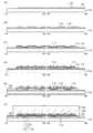
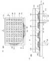
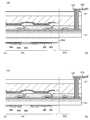
本実施の形態では、本発明の一態様の発光装置100について、図1乃至図4を用いて説
明する。図1(A)は、発光装置100の平面図である。また、図1(B)は、図1(A
)中に一点鎖線A1−A2とA3−A4で示した部位の断面図である。(Embodiment 1)
In the present embodiment, the
) Is a cross-sectional view of the portion shown by the alternate long and short dash lines A1-A2 and A3-A4.
<発光装置の構成例>
本実施の形態では、発光装置100として、ボトムエミッション構造(下面射出構造)の
発光装置を例示する。発光装置100は、マトリクス状に配置された複数の発光部132
を有する。図1(A)に、マトリクス状に配置された発光部132が形成されている領域
を領域130として示す。領域130において、発光部132が形成されていない領域は
可視光を透過する。領域130において、発光部132が形成されていない領域を、透光
部131と呼ぶ。<Configuration example of light emitting device>
In the present embodiment, as the
Have. FIG. 1A shows a region in which light emitting
本実施の形態に例示する発光装置100は、接着層120を介して基板111と基板12
1が貼り合わさった構造を有する。また、発光装置100は、基板111上に電極115
を有し、電極115上に複数の隔壁114を有する。また、電極115および隔壁114
上にEL層117を有し、EL層117上に電極118を有する。また、電極118上に
電極119を有する。The
It has a structure in which 1 is bonded. Further, the
And having a plurality of
It has an
発光部132は発光素子125を有する。電極115、EL層117、および電極118
が重畳し、かつ、電極115とEL層117、並びに、EL層117と電極118が接し
ている領域が、発光素子125として機能する。The
The regions in which the
発光装置100を動作させるための信号は、端子141および端子142を介して発光装
置100に入力される。端子141は電極115と電気的に接続し、端子142は電極1
19と電気的に接続する。なお、本実施の形態に例示する発光装置100では、電極11
5の一部を端子141として機能させ、電極119の一部を端子142として機能させる
例を示しているが、端子141および端子142として機能する電極を、別途形成しても
よい。The signal for operating the
Electrically connect to 19. In the
Although a part of 5 is made to function as a terminal 141 and a part of the
また、マトリクス状に配置された複数の発光部132が形成されている領域130におい
て、電極118が形成されていない領域が透光部131として機能する。発光装置100
では、透光部131が網目状に形成されている。Further, in the
, The
基板121側から発光装置100に入射する光191は、透光部131を介して基板11
1側に透過する。すなわち、透光部131を介して、基板121側の様子を基板111側
で観察することができる。また、発光装置100はボトムエミッション構造の発光装置で
あるため、発光素子125から発せられた光192は、基板111側に射出される。The light 191 incident on the
It penetrates to one side. That is, the state of the
発光部132から光192を発することにより、発光装置100を照明装置として機能さ
せることができる。また、発光部132から発せられた光192は、拡散することにより
基板121から入射した光191と干渉する。発光部132から光192を発することに
より、基板121側の様子を見えなくすることができる。By emitting light 192 from the
また、透光部131と発光部132の合計占有面積(領域130の面積)に対する透光部
131の占有面積の百分率(以下、「透光率」ともいう。)は、80%以下が好ましく、
50%以下がより好ましく、20%以下がさらに好ましい。透光率が小さいほど、領域1
30をより均一に発光させることができる。一方で、透光率が大きいと、基板121側の
様子をより明確に視認することができる。Further, the percentage of the occupied area of the translucent portion 131 (hereinafter, also referred to as “translucency”) with respect to the total occupied area (area of the region 130) of the
50% or less is more preferable, and 20% or less is further preferable. The smaller the light transmittance, the
30 can be made to emit light more uniformly. On the other hand, when the light transmittance is large, the state of the
また、図1に、隣接する2つの発光部132の中心から中心までの距離をピッチPとして
示す。ピッチPを小さくすると、基板121側の様子をより明確に視認することができる
。また、ピッチPを小さくすると、発光部132をより均一に発光させることができる。
ピッチPは、1cm以下が好ましく、5mm以下がより好ましく、1mm以下がさらに好
ましい。Further, FIG. 1 shows the distance from the center to the center of two adjacent
The pitch P is preferably 1 cm or less, more preferably 5 mm or less, and even more preferably 1 mm or less.
また、1インチ当たりの発光部132の数を200個以上(200dpi以上、ピッチP
換算で約127μm以下)、好ましくは300個以上(300dpi以上、ピッチP換算
で約80μm以下)とすると、発光部132から発せられた光の均一性と、基板121側
の視認性を良好なものとすることができる。In addition, the number of light emitting
When the number is about 127 μm or less in terms of conversion, preferably 300 or more (300 dpi or more, about 80 μm or less in terms of pitch P), the uniformity of the light emitted from the
なお、本実施の形態では、ボトムエミッション構造(下面射出構造)の発光装置について
例示するが、トップエミッション構造(上面射出構造)、またはデュアルエミッション構
造(両面射出構造)の発光装置とすることもできる。In the present embodiment, a light emitting device having a bottom emission structure (bottom injection structure) is illustrated, but a light emitting device having a top emission structure (top injection structure) or a dual emission structure (double-sided injection structure) can also be used. ..
<発光装置の作製工程例>
次に、図2を用いて、発光装置100の作製工程例について説明する。図2は、図1(A
)中に一点鎖線A1−A2とA3−A4で示した部位の断面図である。<Example of manufacturing process of light emitting device>
Next, an example of a manufacturing process of the
) Is a cross-sectional view of the portion shown by the alternate long and short dash lines A1-A2 and A3-A4.
[基板111、基板121について]
基板111および基板121としては、少なくとも後の熱処理に耐えうる程度の耐熱性を
有し、可視光を透過する材料を用いることができる。例えば、ガラス基板、石英基板など
を用いることができる。また、プラスチックなどの有機樹脂材料を用いると、発光装置1
00に可撓性を付与することができる。なお、可撓性を有する程度の厚さのガラス基板、
または石英基板などを用いてもよい。[About
As the
Flexibility can be imparted to 00. A glass substrate with a thickness sufficient to have flexibility,
Alternatively, a quartz substrate or the like may be used.
基板121および基板111に用いることができる有機樹脂材料としては、ポリエチレン
テレフタレート樹脂、ポリエチレンナフタレート樹脂、ポリアクリロニトリル樹脂、ポリ
イミド樹脂、ポリメチルメタクリレート樹脂、ポリカーボネート樹脂、ポリエーテルスル
フォン樹脂、ポリアミド樹脂、シクロオレフィン樹脂、ポリスチレン樹脂、ポリアミドイ
ミド樹脂、ポリ塩化ビニル樹脂、などがある。Examples of the organic resin material that can be used for the
また、基板121および基板111の熱膨張係数は、好ましくは30ppm/K以下、さ
らに好ましくは10ppm/K以下とする。また、基板121および基板111の表面に
、予め窒化シリコンや酸化窒化シリコン等の窒素と珪素を含む膜や窒化アルミニウム等の
窒素とアルミニウムを含む膜のような透水性の低い保護膜を成膜しておいても良い。なお
、基板121および基板111として、繊維体に有機樹脂が含浸された構造物(所謂、プ
リプレグとも言う)を用いてもよい。The coefficient of thermal expansion of the
このような基板を用いることにより、割れにくい表示装置を提供することができる。また
は、軽量な表示装置を提供することができる。または、曲げやすい表示装置を提供するこ
とができる。By using such a substrate, it is possible to provide a display device that is hard to break. Alternatively, a lightweight display device can be provided. Alternatively, a bendable display device can be provided.
[電極115の形成]
基板111上に電極115を形成する(図2(A)参照。)。本実施の形態に示す発光装
置100では、電極115を陽極として用いる。よって、電極115として、インジウム
錫酸化物などのEL層117よりも仕事関数が大きく透光性を有する材料を用いる。[Formation of electrode 115]
The
まず、基板111上に、電極115を形成するための導電膜を設ける。該導電膜は、プラ
ズマCVD法、LPCVD法、メタルCVD法、またはMOCVD法などのCVD法や、
ALD法、スパッタリング法、蒸着法などにより形成することができる。なお、導電膜を
MOCVD法などのプラズマを用いない方法で成膜すると、被形成面へのダメージを少な
くすることができる。First, a conductive film for forming the
It can be formed by an ALD method, a sputtering method, a vapor deposition method, or the like. If the conductive film is formed by a method such as the MOCVD method that does not use plasma, damage to the surface to be formed can be reduced.
本実施の形態では、電極115を形成するための導電膜として、スパッタリング法により
インジウム錫酸化膜を成膜する。In the present embodiment, an indium tin oxide film is formed by a sputtering method as a conductive film for forming the
次に導電膜上にフォトリソグラフィ工程によりレジストマスクを形成し、レジストマスク
を用いて導電膜の一部をエッチングして、電極115を形成する。レジストマスクの形成
は、印刷法、インクジェット法などにより行うこともできる。レジストマスクをインクジ
ェット法で形成すると、フォトマスクを使用しないため、製造コストを低減できる。Next, a resist mask is formed on the conductive film by a photolithography step, and a part of the conductive film is etched with the resist mask to form the
導電膜のエッチングは、ドライエッチング法でもウエットエッチング法でもよく、両方を
用いてもよい。なお、ドライエッチング法によりエッチングを行った場合、レジストマス
クを除去する前にアッシング処理を行うと、剥離液を用いたレジストマスクの除去を容易
とすることができる。The conductive film may be etched by a dry etching method or a wet etching method, or both may be used. When etching is performed by the dry etching method, it is possible to easily remove the resist mask using a stripping solution by performing an ashing treatment before removing the resist mask.
なお、電極115は、上記形成方法の代わりに、電解メッキ法、印刷法、インクジェット
法等で形成してもよい。The
また、本実施の形態に示す発光装置100では、電極115の一部を端子141として用
いる。Further, in the
[隔壁114の形成]
次に、電極115上に隔壁114を形成する(図2(B)参照)。隔壁114は、可視光
を透過する絶縁性材料を用いて形成する。例えば、隔壁114は、酸化シリコン、窒化シ
リコン、酸化窒化シリコン、窒化酸化シリコン、酸化アルミニウム、酸化窒化アルミニウ
ム、窒化酸化アルミニウムなどの無機材料や、エポキシ樹脂、アクリル樹脂、イミド樹脂
などの有機樹脂材料を用いて形成することができる。また、隔壁114は、これらの材料
を積層した多層構造としてもよい。[Formation of partition wall 114]
Next, the
隔壁114を設けることにより、透光部131が意図せず発光することを防ぐことができ
る。By providing the
隔壁114は、プラズマCVD法、LPCVD法、メタルCVD法、またはMOCVD法
などのCVD法や、ALD法、スパッタリング法、蒸着法、熱酸化法、塗布法、印刷法な
どにより形成することができる。The
まず、電極115上に、隔壁114を形成するための絶縁膜を設ける。本実施の形態では
、該絶縁膜として、塗布法により成膜した感光性のイミド樹脂を用いる。なお、感光を有
する材料を用いて隔壁114を形成すると、レジストマスクの形成工程と、エッチング工
程を省略することができる。First, an insulating film for forming the
隔壁114は、その側壁がテーパー状、階段状または連続した曲率を持って形成される傾
斜面となるように形成することが好ましい。隔壁114の側壁をこのような形状とするこ
とで、後に形成されるEL層117や電極118の被覆性を良好なものとすることができ
る。The
[EL層117の形成]
次に、電極115および隔壁114上にEL層117を形成する(図2(C)参照。)。
EL層117の一部は、電極115の一部と接して形成する。なお、EL層117の構成
については、実施の形態5で説明する。[Formation of EL layer 117]
Next, the
A part of the
[電極118の形成]
次に、EL層117上に電極118を形成する(図2(D)参照。)。本実施の形態では
電極118を陰極として用いるため、電極118をEL層117に電子を注入できる仕事
関数の小さい材料を用いて形成することが好ましい。また、仕事関数の小さい金属単層で
はなく、仕事関数の小さいアルカリ金属、またはアルカリ土類金属を数nm形成した層を
緩衝層として形成し、その上に、アルミニウム(Al)、チタン(Ti)、タンタル(T
a)、タングステン(W)、モリブデン(Mo)、クロム(Cr)、マクネシウム(Mg
)などの金属材料、インジウム錫酸化物等の導電性を有する酸化物材料、または半導体材
料を積層して形成してもよい。また、緩衝層として、アルカリ土類金属の酸化物、ハロゲ
ン化物、または、マグネシウム−銀等の合金を用いることもできる。[Formation of electrode 118]
Next, the
a), Tungsten (W), Molybdenum (Mo), Chromium (Cr), Macnesium (Mg)
), A conductive oxide material such as indium tin oxide, or a semiconductor material may be laminated and formed. Further, as the buffer layer, an oxide of an alkaline earth metal, a halide, or an alloy such as magnesium-silver can also be used.
本実施の形態では、電極118としてアルミニウムとチタンの積層を用いる。電極118
は、メタルマスクを用いた蒸着法により形成することができる。また、本実施の形態では
、EL層117に電子を注入しやすくするため、EL層117と電極118の間に、厚さ
数nmのフッ化リチウムを形成する。本実施の形態で用いるメタルマスクは、マトリクス
状に配置された複数の開口部を有する金属板である。まず、該メタルマスクを介してフッ
化リチウムを蒸着し、続いてアルミニウムを蒸着し、続いてチタンを蒸着することにより
、EL層117上の該メタルマスクが有する開口部と重畳する位置に、フッ化リチウムと
電極118を形成することができる。In this embodiment, a laminate of aluminum and titanium is used as the
Can be formed by a vapor deposition method using a metal mask. Further, in the present embodiment, lithium fluoride having a thickness of several nm is formed between the
[電極119の形成]
次に、EL層117および電極118上に、電極119を形成する(図2(E)参照。)
。電極119は、電極115と同様の材料および方法により形成することができる。電極
119により、複数の電極118が電気的に接続される。端子142から入力された信号
は、電極119を介して電極118に伝達される。[Formation of electrode 119]
Next, the
.. The
また、本実施の形態に示す発光装置100では、電極119の一部を端子142として用
いる。Further, in the
[基板121を貼り合わせる]
次に、基板111上に、接着層120を介して基板121を形成する(図2(F)参照。
)。接着層120としては、光硬化型の接着剤、反応硬化型接着剤、熱硬化型接着剤、ま
たは嫌気型接着剤を用いることができる。例えば、エポキシ樹脂、アクリル樹脂、イミド
樹脂等を用いることができる。接着層120に乾燥剤(ゼオライト等)を混ぜてもよい。
なお、端子141および端子142上には、接着層120および基板121は形成しない
。[Attach the substrate 121]
Next, the
). As the
The
このようにして、発光装置100を作製することができる。In this way, the
<発光装置の変形例1>
本実施の形態に示したボトムエミッション構造の発光装置100を変形し、トップエミッ
ション構造の発光装置100とすることができる。<Modification example 1 of light emitting device>
The
ボトムエミッション構造の発光装置100をトップエミッション構造の発光装置100と
する場合は、電極115を、光を反射する機能を有する材料を用いて形成し、電極118
を、光を透過する機能を有する材料を用いて形成する。トップエミッション構造の発光装
置100では、発光素子125から発せられた光192は、基板121側に射出する。When the
Is formed using a material having a function of transmitting light. In the
なお、電極115および電極118は、単層に限らず複数層の積層構造としてもよい。例
えば、電極115を陽極として用いる場合、EL層117と接する層を、インジウム錫酸
化物などのEL層117よりも仕事関数が大きく透光性を有する層とし、その層に接して
反射率の高い層(アルミニウム、アルミニウムを含む合金、または銀など)を設けてもよ
い。The
<発光装置の変形例2>
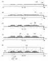
光192が射出される側の発光部132と重畳する位置に、マイクロレンズアレイ981
を設けてもよい(図3(A)参照)。また、発光部132と重畳する位置に、光拡散フィ
ルム982を設けてもよい(図3(B)参照)。<Modification example 2 of light emitting device>
The
May be provided (see FIG. 3 (A)). Further, the
マイクロレンズアレイ981または光拡散フィルム982を介して光192を射出するこ
とで、光192をより拡散させることができる。よって、領域130をより均一に発光さ
せることができる。
<発光装置の変形例3>
図4(A)に示すように、発光装置100において、基板111側に、タッチセンサを有
する基板を設けてもよい。タッチセンサは、導電層991と導電層993などを用いて構
成されている。また、それらの間には、絶縁層992が設けられている。<Modification example 3 of light emitting device>
As shown in FIG. 4A, in the
なお、導電層991、及び/又は、導電層993は、インジウム錫酸化物やインジウム亜
鉛酸化物などの透明導電膜を用いることが望ましい。ただし、抵抗を下げるため、導電層
991、及び/又は、導電層993の一部、または、全部に、低抵抗な材料を持つ層を用
いてもよい。例えば、アルミニウム、チタン、クロム、ニッケル、銅、イットリウム、ジ
ルコニウム、モリブデン、銀、タンタル、またはタングステンからなる単体金属、または
これを主成分とする合金を単層構造または積層構造を用いることができる。または、導電
層991、及び/又は、導電層993として、金属ナノワイヤを用いてもよい。その場合
の金属としては、銀などが好適である。これにより、抵抗値を下げることが出来るため、
センサの感度を向上させることが出来る。For the
The sensitivity of the sensor can be improved.
絶縁層992は、酸化シリコン、窒化シリコン、酸化窒化シリコン、窒化酸化シリコン、
酸化アルミニウム、酸化窒化アルミニウム、または窒化酸化アルミニウム等を、単層また
は多層で形成するのが好ましい。絶縁層992は、スパッタリング法やCVD法、熱酸化
法、塗布法、印刷法等を用いて形成することが可能である。The insulating
It is preferable to form aluminum oxide, aluminum nitride, aluminum nitride, or the like in a single layer or multiple layers. The insulating
なお、図4(A)ではタッチセンサを有する基板994を基板111側に設ける例を示し
ているが、本発明の実施形態の一態様は、これに限定されない。タッチセンサは基板12
1側に設けることもできる。Although FIG. 4A shows an example in which the
It can also be provided on one side.
なお、基板994として、光学フィルムの機能を持たせてもよい。つまり、基板994は
、偏光板や位相差板などの機能を有していてもよい。The
また、図4(B)に示すように、基板111に直接タッチセンサを形成してもよい。Further, as shown in FIG. 4B, the touch sensor may be formed directly on the
本実施の形態は、他の実施の形態に記載した構成と適宜組み合わせて実施することが可能
である。This embodiment can be implemented in combination with the configurations described in other embodiments as appropriate.
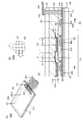
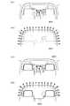
(実施の形態2)
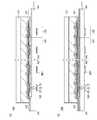
本実施の形態では、発光装置100と異なる構成を有する発光装置150について、図5
乃至図8を用いて説明する。図5(A)は、発光装置150の平面図である。また、図5
(B)は、図5(A)中に一点鎖線B1−B2とB3−B4で示した部位の断面図である
。なお、同じ説明の繰り返しを少なくするため、本実施の形態では、主に発光装置100
と異なる部分について説明する。(Embodiment 2)
In the present embodiment, the
This will be described with reference to FIG. FIG. 5A is a plan view of the
(B) is a cross-sectional view of the portion shown by the alternate long and short dash line B1-B2 and B3-B4 in FIG. 5 (A). In order to reduce the repetition of the same description, in the present embodiment, the
The part different from is explained.
<発光装置の構成例>
本実施の形態では、発光装置150として、ボトムエミッション構造の発光装置を例示す
る。発光装置150は、網目状に配置された発光部132と、マトリクス状に配置された
複数の透光部131を有する。透光部131は、可視光を透過することができる。なお、
電極118が形成されていない領域が透光部131として機能する。<Configuration example of light emitting device>
In the present embodiment, as the
The region where the
本実施の形態に例示する発光装置150は、接着層120を介して基板111と基板12
1が貼り合わさった構造を有する。また、発光装置150は、基板111上に電極115
を有し、電極115上にEL層117を有し、EL層117上に電極118を有する。発
光装置150が有する電極118は、水平方向に延伸した形状の電極118Hと、垂直方
向に延伸した形状の電極118Vを含む。本実施の形態において、単に電極118として
示す場合は、電極118Hおよび電極118Vのどちらか一方、または、電極118Hお
よび電極118Vの両方を示す。The
It has a structure in which 1 is bonded. Further, the
With an
また、本実施の形態に例示する発光装置150では、電極115の一部を端子141とし
て機能させ、電極118の一部を端子142として機能させる例を示しているが、端子1
41および端子142として機能する電極を、別途形成してもよい。Further, in the
Electrodes that function as 41 and
実施の形態1に例示した発光装置100と同様に、基板121側から発光装置150に入
射する光191は、透光部131を介して基板111側に透過する。すなわち、透光部1
31を介して、基板121側の様子を基板111側で観察することができる。また、発光
装置150はボトムエミッション構造の発光装置であるため、発光素子125から発せら
れた光192は、基板111側に射出される。また、発光装置150は、発光部132が
網目状に発光するため、領域130内の発光強度分布の均一性が高い。よって、本発明の
一態様の発光装置150によれば、均一性の良好な面光源を有する照明装置を実現するこ
とができる。Similar to the
The state of the
また、実施の形態1に例示した発光装置100と同様に、透光部131と発光部132の
合計占有面積に対する透光部131の占有面積の百分率(以下、「透光率」ともいう。)
は、80%以下が好ましく、50%以下がより好ましく、20%以下がさらに好ましい。
透光率が小さいほど、領域130をより均一に発光させることができる。一方で、透光率
が大きいと、基板121側の様子をより明確に視認することができる。Further, similarly to the
Is preferably 80% or less, more preferably 50% or less, still more preferably 20% or less.
The smaller the light transmittance, the more uniformly the
また、図5に、隣接する2つの透光部131の中心から中心までの距離をピッチPとして
示す。ピッチPを小さくすると、基板121側の様子をより明確に視認することができる
。また、ピッチPを小さくすると、発光部132をより均一に発光させることができる。
ピッチPは、1cm以下が好ましく、5mm以下がより好ましく、1mm以下がさらに好
ましい。Further, FIG. 5 shows the distance from the center to the center of the two adjacent
The pitch P is preferably 1 cm or less, more preferably 5 mm or less, and even more preferably 1 mm or less.
また、1インチ当たりの透光部131の数を200個以上(200dpi以上、ピッチP
換算で約127μm以下)、好ましくは300個以上(300dpi以上、ピッチP換算
で約80μm以下)とすると、発光部132から発せられた光の均一性と、基板121側
の視認性を良好なものとすることができる。In addition, the number of
When the number is about 127 μm or less in terms of conversion, preferably 300 or more (300 dpi or more, about 80 μm or less in terms of pitch P), the uniformity of the light emitted from the
また、発光部132と重畳する位置に、マイクロレンズアレイや、光拡散フィルムなどを
設けてもよい。Further, a microlens array, a light diffusing film, or the like may be provided at a position where it overlaps with the
なお、本実施の形態では、ボトムエミッション構造(下面射出構造)の発光装置について
例示するが、トップエミッション構造(上面射出構造)、またはデュアルエミッション構
造(両面射出構造)の発光装置とすることもできる。In the present embodiment, a light emitting device having a bottom emission structure (bottom injection structure) is illustrated, but a light emitting device having a top emission structure (top injection structure) or a dual emission structure (double-sided injection structure) can also be used. ..
<発光装置の作製工程例>
次に、図6を用いて、発光装置150の作製工程例について説明する。図6は、図5(A
)中に一点鎖線B1−B2とB3−B4で示した部位の断面図である。<Example of manufacturing process of light emitting device>
Next, an example of a manufacturing process of the
) Is a cross-sectional view of the portion shown by the alternate long and short dash lines B1-B2 and B3-B4.
[基板111、基板121について]
基板111、基板121は、実施の形態1と同様の材料を用いることができる。[About
The same materials as those in the first embodiment can be used for the
[電極115の形成]
基板111上に電極115を形成する(図6(A)参照。)。電極115は、実施の形態
1と同様の材料および方法を用いて形成することができる。[Formation of electrode 115]
The
[EL層117の形成]
次に、電極115上にEL層117を形成する(図6(B)参照。)。なお、EL層11
7の構成については、実施の形態5で説明する。[Formation of EL layer 117]
Next, the
The configuration of 7 will be described in the fifth embodiment.
[電極118の形成]
次に、EL層117上に電極118を形成する。電極118は、実施の形態1と同様の材
料および方法を用いて形成することができる。まず、横方向に延伸した複数の開口部を有
するメタルマスクを介してフッ化リチウムとアルミニウムを蒸着して、電極118Hを形
成する(図6(C)参照。)。続いて、縦方向に延伸した複数の開口部を有するメタルマ
スクを介してフッ化リチウムとアルミニウムを蒸着して、電極118Vを形成する(図6
(D)参照。)。よって、電極118Hと電極118Vは電気的に接続される。[Formation of electrode 118]
Next, the
See (D). ). Therefore, the
また、電極118Hを形成した後、同じメタルマスクを用いて、基板111を水平方向に
90度回転させて、電極118Vを形成することもできる。Further, after forming the
[基板121を貼り合わせる]
次に、実施の形態1と同様に、基板111上に、接着層120を介して基板121を形成
する(図6(E)参照。)。[Attach the substrate 121]
Next, as in the first embodiment, the
このようにして、発光装置150を作製することができる。In this way, the
<発光装置の変形例1>
本実施の形態に示したボトムエミッション構造の発光装置150を変形し、トップエミッ
ション構造の発光装置150とすることができる。<Modification example 1 of light emitting device>
The
ボトムエミッション構造の発光装置150をトップエミッション構造の発光装置150と
する場合は、電極115を、光を反射する機能を有する材料を用いて形成し、電極118
を、光を透過する機能を有する材料を用いて形成する。トップエミッション構造の発光装
置150では、発光素子125から発せられた光192は、基板121側に射出する。When the
Is formed using a material having a function of transmitting light. In the
なお、電極115および電極118は、単層に限らず複数層の積層構造としてもよい。例
えば、電極115を陽極として用いる場合、EL層117と接する層を、インジウム錫酸
化物などのEL層117よりも仕事関数が大きく透光性を有する層とし、その層に接して
反射率の高い層(アルミニウム、アルミニウムを含む合金、または銀など)を設けてもよ
い。The
<発光装置の変形例2>
光192が射出される側の発光部132と重畳する位置に、マイクロレンズアレイ981
を設けてもよい(図7(A)参照)。また、発光部132と重畳する位置に、光拡散フィ
ルム982を設けてもよい(図7(B)参照)。<Modification example 2 of light emitting device>
The
May be provided (see FIG. 7 (A)). Further, the
マイクロレンズアレイ981または光拡散フィルム982を介して光192を射出するこ
とで、光192をより拡散させることができる。よって、領域130をより均一に発光さ
せることができる。The light 192 can be more diffused by emitting the light 192 through the
<発光装置の変形例3>
図8(A)に示すように、発光装置150において、基板111側に、タッチセンサを有
する基板を設けてもよい。タッチセンサは、導電層991と導電層993などを用いて構
成されている。また、それらの間には、絶縁層992が設けられている。<Modification example 3 of light emitting device>
As shown in FIG. 8A, in the
なお、導電層991、及び/又は、導電層993は、インジウム錫酸化物やインジウム亜
鉛酸化物などの透明導電膜を用いることが望ましい。ただし、抵抗を下げるため、導電層
991、及び/又は、導電層993の一部、または、全部に、低抵抗な材料を持つ層を用
いてもよい。例えば、アルミニウム、チタン、クロム、ニッケル、銅、イットリウム、ジ
ルコニウム、モリブデン、銀、タンタル、またはタングステンからなる単体金属、または
これを主成分とする合金を単層構造または積層構造を用いることができる。または、導電
層991、及び/又は、導電層993として、金属ナノワイヤを用いてもよい。その場合
の金属としては、銀などが好適である。これにより、抵抗値を下げることが出来るため、
センサの感度を向上させることが出来る。For the
The sensitivity of the sensor can be improved.
絶縁層992は、酸化シリコン、窒化シリコン、酸化窒化シリコン、窒化酸化シリコン、
酸化アルミニウム、酸化窒化アルミニウム、または窒化酸化アルミニウム等を、単層また
は多層で形成するのが好ましい。絶縁層992は、スパッタリング法やCVD法、熱酸化
法、塗布法、印刷法等を用いて形成することが可能である。The insulating
It is preferable to form aluminum oxide, aluminum nitride, aluminum nitride, or the like in a single layer or multiple layers. The insulating
なお、図8(A)ではタッチセンサを基板111側に設ける例を示しているが、本発明の
実施形態の一態様は、これに限定されない。タッチセンサは基板121側に設けることも
できる。Although FIG. 8A shows an example in which the touch sensor is provided on the
なお、基板994として、光学フィルムの機能を持たせてもよい。つまり、基板994は
、偏光板や位相差板などの機能を有していてもよい。The
また、図8(B)に示すように、基板111に直接タッチセンサを形成してもよい。Further, as shown in FIG. 8B, the touch sensor may be formed directly on the
本実施の形態は、他の実施の形態に記載した構成と適宜組み合わせて実施することが可能
である。This embodiment can be implemented in combination with the configurations described in other embodiments as appropriate.
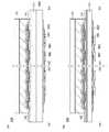
(実施の形態3)
本実施の形態では、発光装置100および発光装置150と異なる構成を有する発光装置
200について、図9乃至図11を用いて説明する。図9(A)は、発光装置200の平
面図である。また、図9(B)は、図9(A)中に一点鎖線C1−C2とC3−C4で示
した部位の断面図である。なお、同じ説明の繰り返しを少なくするため、本実施の形態で
は、主に発光装置100および発光装置150と異なる部分について説明する。(Embodiment 3)
In the present embodiment, the
<発光装置の構成例>
本実施の形態では、発光装置200として、ボトムエミッション構造の発光装置を例示す
る。発光装置200は、マトリクス状に配置された複数の発光部132を有する。図9(
A)に、マトリクス状に配置された発光部132が形成されている領域を領域130とし
て示す。領域130において、発光部132が形成されていない領域は可視光を透過する
。領域130において、発光部132が形成されていない領域を、透光部131と呼ぶ。<Configuration example of light emitting device>
In the present embodiment, as the
In A), a region in which light emitting
本実施の形態に例示する発光装置200は、接着層120を介して基板111と基板12
1が貼り合わさった構造を有する。また、発光装置200は、基板111上にストライプ
状の電極115を複数有し、電極115上にEL層117を有し、EL層117上に電極
118を有する。また、電極118上にストライプ状の電極119を複数有する。図9(
A)では、電極115が縦方向に延伸し、電極119が横方向に延伸している例を示して
いる。電極115と電極119の延伸方向は直交している。The
It has a structure in which 1 is bonded. Further, the
A) shows an example in which the
電極115と電極119が重畳する領域が発光部132として機能する。また、電極11
8は、電極115と電極119が重畳する領域に形成される。発光部132は発光素子1
25を有する。電極115、EL層117、および電極118が重畳する領域が、発光素
子125として機能する。The region where the
Reference numeral 8 is formed in a region where the
Has 25. The region on which the
発光装置200を動作させるための信号は、端子141および端子142を介して発光装
置200に入力される。端子141は電極115と電気的に接続し、端子142は電極1
19と電気的に接続する。発光装置200は複数の電極115を有し、複数の電極115
それぞれに、端子141を介して異なる信号、もしくは同じ信号を供給することができる
。発光装置200は複数の電極119を有し、複数の電極119それぞれに、端子142
を介して異なる信号、もしくは同じ信号を供給することができる。なお、本実施の形態に
例示する発光装置200では、電極115の一部を端子141として機能させ、電極11
9の一部を端子142として機能させる例を示しているが、端子141および端子142
として機能する電極を、別途形成してもよい。The signal for operating the
Electrically connect to 19. The
Different signals or the same signal can be supplied to each via the
Different signals or the same signal can be supplied via. In the
An example in which a part of 9 is made to function as a terminal 142 is shown, but the terminal 141 and the terminal 142
An electrode that functions as an electrode may be formed separately.
また、マトリクス状に配置された複数の発光部132が形成されている領域130におい
て、電極118が形成されていない領域が透光部131として機能する。発光装置200
では、透光部131が網目状に形成されている。Further, in the
, The
基板121側から発光装置200に入射する光191は、透光部131を介して基板11
1側に透過する。すなわち、透光部131を介して、基板121側の様子を基板111側
で観察することができる。また、発光装置200はボトムエミッション構造の発光装置で
あるため、発光素子125から発せられた光192は、基板111側に射出される。The light 191 incident on the
It penetrates to one side. That is, the state of the
複数の電極115と、複数の電極119それぞれを適宜選択して信号を供給することで、
電極115と電極119の交差部に存在する任意の発光素子125を任意の輝度で発光さ
せることができる。複数の発光素子125を任意の輝度で点灯、または消灯させることに
より、領域130に文字や映像を表示することができる。よって、本実施の形態に示す発
光装置200は、照明装置としてだけでなく、表示装置としても機能することができる。By appropriately selecting each of the plurality of
Any
また、透光部131と発光部132の合計占有面積(領域130の面積)に対する透光部
131の占有面積の百分率(以下、「透光率」ともいう。)は、80%以下が好ましく、
50%以下がより好ましく、20%以下がさらに好ましい。透光率が小さいほど、領域1
30をより均一に発光させることができ、表示品位の良好な映像を表示させることができ
る。一方で、透光率が大きいと、基板121側の様子をより明確に視認することができる
。Further, the percentage of the occupied area of the translucent portion 131 (hereinafter, also referred to as “translucency”) with respect to the total occupied area (area of the region 130) of the
50% or less is more preferable, and 20% or less is further preferable. The smaller the light transmittance, the
30 can be made to emit light more uniformly, and an image having good display quality can be displayed. On the other hand, when the light transmittance is large, the state of the
また、図9に、隣接する2つの発光部132の中心から中心までの距離をピッチPとして
示す。ピッチPを小さくすると、基板121側の様子をより明確に視認することができる
。また、ピッチPを小さくすると、発光部132をより均一に発光させることができる。
ピッチPは、1cm以下が好ましく、5mm以下がより好ましく、1mm以下がさらに好
ましい。Further, FIG. 9 shows the distance from the center of the two adjacent
The pitch P is preferably 1 cm or less, more preferably 5 mm or less, and even more preferably 1 mm or less.
また、1インチ当たりの発光部132の数を200個以上(200dpi以上、ピッチP
換算で約127μm以下)、好ましくは300個以上(300dpi以上、ピッチP換算
で約80μm以下)とすると、発光部132から発せられた光の均一性と、基板121側
の視認性を良好なものとすることができる。また、表示品位の良好な映像を表示させるこ
とができる。In addition, the number of light emitting
When the number is about 127 μm or less in terms of conversion, preferably 300 or more (300 dpi or more, about 80 μm or less in terms of pitch P), the uniformity of the light emitted from the
また、発光部132と重畳する位置に、マイクロレンズアレイや、光拡散フィルムなどを
設けてもよい。Further, a microlens array, a light diffusing film, or the like may be provided at a position where it overlaps with the
なお、本実施の形態では、ボトムエミッション構造(下面射出構造)の発光装置について
例示するが、トップエミッション構造(上面射出構造)、またはデュアルエミッション構
造(両面射出構造)の発光装置とすることもできる。In the present embodiment, a light emitting device having a bottom emission structure (bottom injection structure) is illustrated, but a light emitting device having a top emission structure (top injection structure) or a dual emission structure (double-sided injection structure) can also be used. ..
<発光装置の作製工程例>
次に、図10を用いて、発光装置200の作製工程例について説明する。図10は、図9
(A)中に一点鎖線C1−C2とC3−C4で示した部位の断面図である。<Example of manufacturing process of light emitting device>
Next, an example of a manufacturing process of the
It is sectional drawing of the part shown by the alternate long and short dash line C1-C2 and C3-C4 in (A).
[基板111、基板121について]
基板111、基板121は、実施の形態1と同様の材料を用いることができる。[About
The same materials as those in the first embodiment can be used for the
[電極115の形成]
基板111上に電極115を形成する(図10(A)参照。)。電極115は、実施の形
態1と同様の材料および方法を用いて形成することができる。[Formation of electrode 115]
The
[EL層117の形成]
次に、電極115上にEL層117を形成する(図10(B)参照。)。なお、EL層1
17の構成については、実施の形態5で説明する。[Formation of EL layer 117]
Next, the
The configuration of 17 will be described in the fifth embodiment.
[電極118の形成]
次に、EL層117上に電極118を形成する(図10(C)参照。)。電極118は、
実施の形態1と同様の材料および方法を用いて形成することができる。[Formation of electrode 118]
Next, the
It can be formed using the same materials and methods as in
[電極119の形成]
次に、EL層117および電極118上に、電極119を形成する(図10(D)参照。
)。電極119は、電極115と同様の材料および方法により形成することができる。ま
た、電極119と重畳する複数の電極118は、互いに電気的に接続される。なお、電極
119の形成時に、EL層117の一部が除去される場合がある。[Formation of electrode 119]
Next, the
). The
また、本実施の形態では、電極119の一部を端子142として機能させる例を示してい
る。端子142から入力された信号は、電極119を介して電極118に伝達される。Further, in the present embodiment, an example in which a part of the
[基板121を貼り合わせる]
次に、実施の形態1と同様に、基板111上に、接着層120を介して基板121を形成
する(図10(E)参照。)。[Attach the substrate 121]
Next, as in the first embodiment, the
このようにして、発光装置200を作製することができる。In this way, the
<発光装置の変形例1>
本実施の形態に示したボトムエミッション構造の発光装置200を変形し、トップエミッ
ション構造の発光装置200とすることができる。<Modification example 1 of light emitting device>
The
ボトムエミッション構造の発光装置200をトップエミッション構造の発光装置200と
する場合は、電極115を、光を反射する機能を有する材料を用いて形成し、電極118
を、光を透過する機能を有する材料を用いて形成する。トップエミッション構造の発光装
置200では、発光素子125から発せられた光192は、基板121側に射出する。When the
Is formed using a material having a function of transmitting light. In the
なお、電極115および電極118は、単層に限らず複数層の積層構造としてもよい。例
えば、電極115を陽極として用いる場合、EL層117と接する層を、インジウム錫酸
化物などのEL層117よりも仕事関数が大きく透光性を有する層とし、その層に接して
反射率の高い層(アルミニウム、アルミニウムを含む合金、または銀など)を設けてもよ
い。The
<発光装置の変形例2>
図11(A)に示すように、発光装置200において、基板111側に、タッチセンサを
有する基板を設けてもよい。タッチセンサは、導電層991と導電層993などを用いて
構成されている。また、それらの間には、絶縁層992が設けられている。<Modification example 2 of light emitting device>
As shown in FIG. 11A, in the
なお、導電層991、及び/又は、導電層993は、インジウム錫酸化物やインジウム亜
鉛酸化物などの透明導電膜を用いることが望ましい。ただし、抵抗を下げるため、導電層
991、及び/又は、導電層993の一部、または、全部に、低抵抗な材料を持つ層を用
いてもよい。例えば、アルミニウム、チタン、クロム、ニッケル、銅、イットリウム、ジ
ルコニウム、モリブデン、銀、タンタル、またはタングステンからなる単体金属、または
これを主成分とする合金を単層構造または積層構造を用いることができる。または、導電
層991、及び/又は、導電層993として、金属ナノワイヤを用いてもよい。その場合
の金属としては、銀などが好適である。これにより、抵抗値を下げることが出来るため、
センサの感度を向上させることが出来る。For the
The sensitivity of the sensor can be improved.
絶縁層992は、酸化シリコン、窒化シリコン、酸化窒化シリコン、窒化酸化シリコン、
酸化アルミニウム、酸化窒化アルミニウム、または窒化酸化アルミニウム等を、単層また
は多層で形成するのが好ましい。絶縁層992は、スパッタリング法やCVD法、熱酸化
法、塗布法、印刷法等を用いて形成することが可能である。The insulating
It is preferable to form aluminum oxide, aluminum nitride, aluminum nitride, or the like in a single layer or multiple layers. The insulating
なお、図11(A)ではタッチセンサを基板111側に設ける例を示しているが、本発明
の実施形態の一態様は、これに限定されない。タッチセンサは基板121側に設けること
もできる。Although FIG. 11A shows an example in which the touch sensor is provided on the
なお、基板994として、光学フィルムの機能を持たせてもよい。つまり、基板994は
、偏光板や位相差板などの機能を有していてもよい。The
また、図11(B)に示すように、基板111に直接タッチセンサを形成してもよい。Further, as shown in FIG. 11B, the touch sensor may be formed directly on the
本実施の形態は、他の実施の形態に記載した構成と適宜組み合わせて実施することが可能
である。This embodiment can be implemented in combination with the configurations described in other embodiments as appropriate.
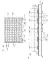
(実施の形態4)
本実施の形態では、発光装置100乃至発光装置200と異なる構成を有する発光装置2
50について、図12乃至図21を用いて説明する。図12(A)は、発光装置250の
斜視図である。本実施の形態に示す発光装置250は、表示領域231、駆動回路232
、および駆動回路233を有する。図12(B)は、図12(A)中に部位231aと示
した表示領域231の一部の拡大図である。また、図12(C)は、図12(A)中に一
点鎖線D1−D2で示した部位の断面図である。なお、同じ説明の繰り返しを少なくする
ため、本実施の形態では、主に発光装置100乃至発光装置200と異なる部分について
説明する。(Embodiment 4)
In the present embodiment, the
50 will be described with reference to FIGS. 12 to 21. FIG. 12A is a perspective view of the
, And a
<発光装置の構成例>
本実施の形態では、発光装置250として、ボトムエミッション構造(下面射出構造)の
発光装置を例示する。発光装置250は、マトリクス状に配置された複数の発光部132
を有する。複数の発光部132が、表示領域231中にマトリクス状に配置されている。
また、発光部132は、電極115、EL層117、および電極118を含む発光素子1
25を有する。また、各発光素子125には、発光素子125の発光量を制御するトラン
ジスタ242が接続されている。表示領域231において、発光部132が形成されてい
ない領域は、可視光を透過する領域を含む。表示領域231において、可視光を透過する
領域を、透光部131と呼ぶ。本実施の形態に例示する発光装置250は、アクティブマ
トリクス型の表示装置として機能する。<Configuration example of light emitting device>
In the present embodiment, as the
Have. A plurality of light emitting
Further, the
Has 25. Further, a
また、発光装置250は、端子電極216を有する。端子電極216は、異方性導電接続
層123を介して外部電極124と電気的に接続されている。また、端子電極216は、
駆動回路232および駆動回路233に電気的に接続されている。Further, the
It is electrically connected to the
駆動回路232および駆動回路233は、複数のトランジスタ252により構成されてい
る。駆動回路232および駆動回路233は、外部電極124から供給された信号を、表
示領域231中のどの発光素子125に供給するかを決定する機能を有する。The
トランジスタ242およびトランジスタ252は、ゲート電極206、ゲート絶縁層20
7、半導体層208、ソース電極209a、ドレイン電極209bを有する。また、ソー
ス電極209a、およびドレイン電極209bと同じ層に、配線219が形成されている
。また、トランジスタ242およびトランジスタ252上に絶縁層210が形成され、絶
縁層210上に絶縁層211が形成されている。また、電極115が絶縁層211上に形
成されている。電極115は、絶縁層210および絶縁層211に形成された開口を介し
てドレイン電極209bに電気的に接続されている。また、電極115上に隔壁114が
形成され、電極115および隔壁114上に、EL層117および電極118が形成され
ている。The
7. It has a
また、発光装置250は、接着層120を介して基板111と基板121が貼り合わされ
た構造を有する。Further, the
また、基板111上には、接着層112を介して絶縁層205が形成されている。絶縁層
205は、酸化シリコン、窒化シリコン、酸化窒化シリコン、窒化酸化シリコン、酸化ア
ルミニウム、酸化窒化アルミニウム、または窒化酸化アルミニウム等を、単層または多層
で形成するのが好ましい。絶縁層205は、スパッタリング法やCVD法、熱酸化法、塗
布法、印刷法等を用いて形成することが可能である。Further, an insulating
なお、絶縁層205は下地層として機能し、基板111や接着層112などから、トラン
ジスタや発光素子への水分や不純物元素の拡散を防止、または低減することができる。The insulating
本実施の形態に例示する発光装置250は、複数の発光素子125を任意の輝度で点灯、
または消灯させることにより、表示領域231に文字や映像を表示することができる。よ
って、本実施の形態に示す発光装置250は、照明装置としてだけでなく、表示装置とし
ても機能することができる。また、本実施の形態に例示する発光装置250は、上記実施
の形態に例示した発光装置200よりも、各発光素子125の発光量をより綿密に制御す
ることができる。In the
Alternatively, by turning off the lights, characters and images can be displayed in the
本発明の一態様によれば、表示品位の良好な表示装置を実現することができる。また、本
発明の一態様によれば、消費電力の少ない表示装置を実現することができる。According to one aspect of the present invention, it is possible to realize a display device having good display quality. Further, according to one aspect of the present invention, it is possible to realize a display device with low power consumption.
また、表示領域231の占有面積に対する透光部131の占有面積の百分率(以下、「透
光率」ともいう。)は、80%以下が好ましく、50%以下がより好ましく、20%以下
がさらに好ましい。透光率が小さいほど、表示領域231をより均一に発光させることが
でき、表示品位の良好な映像を表示させることができる。一方で、透光率が大きいと、基
板121側の様子をより明確に視認することができる。Further, the percentage of the occupied area of the
また、図12(B)に、隣接する2つの発光部132の中心から中心までの距離をピッチ
Pとして示す。ピッチPを小さくすると、基板121側の様子をより明確に視認すること
ができる。また、ピッチPを小さくすると、発光部132をより均一に発光させることが
できる。ピッチPは、1cm以下が好ましく、5mm以下がより好ましく、1mm以下が
さらに好ましい。Further, FIG. 12B shows the distance from the center to the center of the two adjacent
また、1インチ当たりの発光部132の数を200個以上(200dpi以上、ピッチP
換算で約127μm以下)、好ましくは300個以上(300dpi以上、ピッチP換算
で約80μm以下)とすると、発光部132から発せられた光の均一性と、基板121側
の視認性を良好なものとすることができる。また、表示品位の良好な映像を表示させるこ
とができる。In addition, the number of light emitting
When the number is about 127 μm or less in terms of conversion, preferably 300 or more (300 dpi or more, about 80 μm or less in terms of pitch P), the uniformity of the light emitted from the
また、発光部132と重畳する位置に、マイクロレンズアレイや、光拡散フィルムなどを
設けてもよい。Further, a microlens array, a light diffusing film, or the like may be provided at a position where it overlaps with the
なお、本実施の形態では、ボトムエミッション構造(下面射出構造)の発光装置について
例示するが、トップエミッション構造(上面射出構造)、またはデュアルエミッション構
造(両面射出構造)の発光装置とすることもできる。In the present embodiment, a light emitting device having a bottom emission structure (bottom injection structure) is illustrated, but a light emitting device having a top emission structure (top injection structure) or a dual emission structure (double-sided injection structure) can also be used. ..
<画素回路構成例>
次に、図13を用いて、発光装置250のより具体的な構成例について説明する。図13
(A)は、発光装置250の構成を説明するためのブロック図である。発光装置250は
、表示領域231、駆動回路232、および駆動回路233を有する。駆動回路232は
、例えば走査線駆動回路として機能する。また、駆動回路233は、例えば信号線駆動回
路として機能する。<Pixel circuit configuration example>
Next, a more specific configuration example of the
(A) is a block diagram for explaining the structure of the
また、発光装置250は、各々が平行又は略平行に配設され、且つ、駆動回路232によ
って電位が制御されるm本の走査線135と、各々が平行又は略平行に配設され、且つ、
駆動回路233によって電位が制御されるn本の信号線136と、を有する。さらに、表
示領域231はマトリクス状に配設された複数の発光部132を有する。また、駆動回路
232および駆動回路233をまとめて駆動回路部という場合がある。Further, the
It has
各走査線135は、表示領域231においてm行n列に配設された発光部132のうち、
いずれかの行に配設されたn個の発光部132と電気的に接続される。また、各信号線1
36は、m行n列に配設された発光部132のうち、いずれかの列に配設されたm個の発
光部132に電気的に接続される。m、nは、ともに1以上の整数である。Each
It is electrically connected to n
36 is electrically connected to m
〔発光表示装置用画素回路の一例〕
図13(B)は、図13(A)に示す表示装置の発光部132に用いることができる回路
構成を示している。図13(B)に示す発光部132は、トランジスタ431と、容量素
子243と、トランジスタ242と、発光素子125と、を有する。[Example of pixel circuit for light emitting display device]
FIG. 13B shows a circuit configuration that can be used for the
トランジスタ431のソース電極及びドレイン電極の一方は、データ信号が与えられる配
線(以下、信号線DL_nという)に電気的に接続される。さらに、トランジスタ431
のゲート電極は、ゲート信号が与えられる配線(以下、走査線GL_mという)に電気的
に接続される。One of the source electrode and the drain electrode of the
The gate electrode of the above is electrically connected to a wiring (hereinafter, referred to as a scanning line GL_m) to which a gate signal is given.
トランジスタ431は、オン状態またはオフ状態になることにより、データ信号のノード
435への書き込みを制御する機能を有する。The
容量素子243の一対の電極の一方は、ノード435に電気的に接続され、他方は、ノー
ド437に電気的に接続される。また、トランジスタ431のソース電極およびドレイン
電極の他方は、ノード435に電気的に接続される。One of the pair of electrodes of the
容量素子243は、ノード435に書き込まれたデータを保持する保持容量としての機能
を有する。The
トランジスタ242のソース電極及びドレイン電極の一方は、電位供給線VL_aに電気
的に接続され、他方はノード437に電気的に接続される。さらに、トランジスタ242
のゲート電極は、ノード435に電気的に接続される。One of the source electrode and the drain electrode of the
The gate electrode of is electrically connected to the
発光素子125のアノード及びカソードの一方は、電位供給線VL_bに電気的に接続さ
れ、他方は、ノード437に電気的に接続される。One of the anode and cathode of the
発光素子125としては、例えば有機エレクトロルミネセンス素子(有機EL素子ともい
う)などを用いることができる。ただし、発光素子125としては、これに限定されず、
無機材料からなる無機EL素子を用いても良い。As the
An inorganic EL element made of an inorganic material may be used.
なお、電位供給線VL_a及び電位供給線VL_bの一方には、高電源電位VDDが与え
られ、他方には、低電源電位VSSが与えられる。One of the potential supply line VL_a and the potential supply line VL_b is given a high power supply potential VDD, and the other is given a low power supply potential VSS.
図13(B)の発光部132を有する表示装置では、駆動回路232により各行の発光部
132を順次選択し、トランジスタ431をオン状態にしてデータ信号をノード435に
書き込む。In the display device having the
ノード435にデータが書き込まれた発光部132は、トランジスタ431がオフ状態に
なることで保持状態になる。さらに、ノード435に書き込まれたデータの電位に応じて
トランジスタ242のソース電極とドレイン電極の間に流れる電流量が制御され、発光素
子125は、流れる電流量に応じた輝度で発光する。これを行毎に順次行うことにより、
画像を表示できる。The
Images can be displayed.
なお、表示素子として、発光素子125以外の表示素子を適用することも可能である。例
えば、表示素子として、液晶素子、電気泳動素子、電子インク、エレクトロウェッティン
グ素子、MEMS(マイクロ・エレクトロ・メカニカル・システム)、デジタルマイクロ
ミラーデバイス(DMD)、DMS(デジタル・マイクロ・シャッター)、IMOD(イ
ンターフェアレンス・モジュレーション)素子などを用いることも可能である。It is also possible to apply a display element other than the
<発光装置の作製工程例>
次に、図14乃至22を用いて、発光装置100の作製工程例について説明する。図14
乃至22は、図12(A)中に一点鎖線D1−D2で示した部位の断面に相当する図であ
る。<Example of manufacturing process of light emitting device>
Next, an example of a manufacturing process of the
22 to 22 are views corresponding to the cross sections of the portions shown by the alternate long and short dash lines D1-D2 in FIG. 12 (A).
[剥離層113の形成]
まず、素子形成基板101上に剥離層113を形成する(図14(A)参照。)。なお、
素子形成基板101としては、ガラス基板、石英基板、サファイア基板、セラミック基板
、金属基板などを用いることができる。また、本実施の形態の処理温度に耐えうる耐熱性
を有するプラスチック基板を用いてもよい。[Formation of release layer 113]
First, the
As the
また、ガラス基板には、例えば、アルミノシリケートガラス、アルミノホウケイ酸ガラス
、バリウムホウケイ酸ガラスなどのガラス材料が用いられている。なお、酸化バリウム(
BaO)を多く含ませることで、より実用的な耐熱ガラスが得られる。他にも、結晶化ガ
ラスなどを用いることができる。Further, for the glass substrate, for example, glass materials such as aluminosilicate glass, aluminoborosilicate glass, and bariumborosilicate glass are used. Barium oxide (
By containing a large amount of BaO), more practical heat-resistant glass can be obtained. In addition, crystallized glass or the like can be used.
剥離層113は、タングステン、モリブデン、チタン、タンタル、ニオブ、ニッケル、コ
バルト、ジルコニウム、ルテニウム、ロジウム、パラジウム、オスミウム、イリジウム、
シリコンから選択された元素、または前記元素を含む合金材料、または前記元素を含む化
合物材料を用いて形成することができる。また、これらの材料を単層又は積層して形成す
ることができる。なお、剥離層113の結晶構造は、非晶質、微結晶、多結晶のいずれの
場合でもよい。また、剥離層113を、酸化アルミニウム、酸化ガリウム、酸化亜鉛、二
酸化チタン、酸化インジウム、インジウム錫酸化物、インジウム亜鉛酸化物、またはIn
GaZnO(IGZO)等の金属酸化物を用いて形成することもできる。The
It can be formed by using an element selected from silicon, an alloy material containing the element, or a compound material containing the element. Further, these materials can be formed as a single layer or laminated. The crystal structure of the
It can also be formed using a metal oxide such as GaZnO (IGZO).
剥離層113は、スパッタリング法やCVD法、塗布法、印刷法等により形成できる。な
お、塗布法はスピンコーティング法、液滴吐出法、ディスペンス法を含む。The
剥離層113を単層で形成する場合、タングステン、モリブデン、またはタングステンと
モリブデンを含む合金材料を用いることが好ましい。または、剥離層113を単層で形成
する場合、タングステンの酸化物若しくは酸化窒化物、モリブデンの酸化物若しくは酸化
窒化物、またはタングステンとモリブデンを含む合金の酸化物若しくは酸化窒化物を用い
ることが好ましい。When the
また、剥離層113として、例えば、タングステンを含む層とタングステンの酸化物を含
む層の積層構造を形成する場合、タングステンを含む層に接して酸化物絶縁層を形成する
ことで、タングステンを含む層と酸化物絶縁層との界面に、酸化タングステンが形成され
ることを活用してもよい。また、タングステンを含む層の表面を、熱酸化処理、酸素プラ
ズマ処理、オゾン水等の酸化力の強い溶液での処理等を行ってタングステンの酸化物を含
む層を形成してもよい。Further, as the
本実施の形態では、素子形成基板101としてガラス基板を用いる。また、剥離層113
として素子形成基板101上にスパッタリング法によりタングステンを形成する。In this embodiment, a glass substrate is used as the
Tungsten is formed on the
[絶縁層205の形成]
次に、剥離層113上に下地層として絶縁層205を形成する(図14(A)参照。)。
絶縁層205は、酸化シリコン、窒化シリコン、酸化窒化シリコン、窒化酸化シリコン、
酸化アルミニウム、酸化窒化アルミニウム、または窒化酸化アルミニウム等を、単層また
は多層で形成するのが好ましい。例えば、絶縁層205を、酸化シリコンと窒化シリコン
を積層した2層構造としてもよいし、上記材料を組み合わせた5層構造としてもよい。絶
縁層205は、スパッタリング法やCVD法、熱酸化法、塗布法、印刷法等を用いて形成
することが可能である。[Formation of Insulation Layer 205]
Next, an insulating
The insulating
It is preferable to form aluminum oxide, aluminum nitride, aluminum nitride, or the like in a single layer or multiple layers. For example, the insulating
絶縁層205の厚さは、30nm以上500nm以下、好ましくは50nm以上400n
m以下とすればよい。The thickness of the insulating
It may be m or less.
絶縁層205は、素子形成基板101や剥離層113などからの不純物元素の拡散を防止
、または低減することができる。また、素子形成基板101を基板111に換えた後も、
基板111や接着層112などから発光素子125への不純物元素の拡散を防止、または
低減することができる。本実施の形態では、絶縁層205としてプラズマCVD法により
厚さ200nmの酸化窒化シリコンと厚さ50nmの窒化酸化シリコンの積層膜を用いる
。The insulating
It is possible to prevent or reduce the diffusion of impurity elements from the
[ゲート電極206の形成]
次に、絶縁層205上にゲート電極206を形成する(図14(A)参照。)。ゲート電
極206は、アルミニウム、クロム、銅、タンタル、チタン、モリブデン、タングステン
から選ばれた金属元素、または上述した金属元素を成分とする合金か、上述した金属元素
を組み合わせた合金等を用いて形成することができる。また、マンガン、ジルコニウムの
いずれか一または複数から選択された金属元素を用いてもよい。また、ゲート電極206
は、単層構造でも、二層以上の積層構造としてもよい。例えば、シリコンを含むアルミニ
ウム膜の単層構造、チタン膜上にアルミニウム膜を積層する二層構造、窒化チタン膜上に
チタン膜を積層する二層構造、窒化チタン膜上にタングステン膜を積層する二層構造、窒
化タンタル膜または窒化タングステン膜上にタングステン膜を積層する二層構造、チタン
膜上に銅膜を積層する二層構造、チタン膜と、そのチタン膜上にアルミニウム膜を積層し
、さらにその上にチタン膜を形成する三層構造等がある。また、アルミニウムに、チタン
、タンタル、タングステン、モリブデン、クロム、ネオジム、スカンジウムから選ばれた
一または複数を組み合わせた合金膜、もしくは窒化膜を用いてもよい。[Formation of gate electrode 206]
Next, the
May be a single-layer structure or a laminated structure having two or more layers. For example, a single-layer structure of an aluminum film containing silicon, a two-layer structure in which an aluminum film is laminated on a titanium film, a two-layer structure in which a titanium film is laminated on a titanium nitride film, and a tungsten film on which a titanium nitride film is laminated. Layer structure, two-layer structure in which a tungsten film is laminated on a tantalum nitride film or a tungsten nitride film, a two-layer structure in which a copper film is laminated on a titanium film, a titanium film and an aluminum film laminated on the titanium film, and further There is a three-layer structure or the like that forms a titanium film on it. Further, an alloy film or a nitride film in which one or more selected from titanium, tantalum, tungsten, molybdenum, chromium, neodymium, and scandium may be combined with aluminum may be used.
また、ゲート電極206は、インジウム錫酸化物、酸化タングステンを含むインジウム酸
化物、酸化タングステンを含むインジウム亜鉛酸化物、酸化チタンを含むインジウム酸化
物、酸化チタンを含むインジウム錫酸化物、インジウム亜鉛酸化物、酸化シリコンを添加
したインジウム錫酸化物等の透光性を有する導電性材料を適用することもできる。また、
上記透光性を有する導電性材料と、上記金属元素の積層構造とすることもできる。Further, the
It is also possible to form a laminated structure of the above-mentioned conductive material having translucency and the above-mentioned metal element.
まず、絶縁層205上にスパッタリング法、CVD法、蒸着法等により、後にゲート電極
206となる導電膜を積層し、該導電膜上にフォトリソグラフィ工程によりレジストマス
クを形成する。次に、レジストマスクを用いてゲート電極206となる導電膜の一部をエ
ッチングして、ゲート電極206を形成する。この時、他の配線および電極も同時に形成
することができる。First, a conductive film to be a
導電膜のエッチングは、ドライエッチング法でもウエットエッチング法でもよく、両方を
用いてもよい。なお、ドライエッチング法によりエッチングを行った場合、レジストマス
クを除去する前にアッシング処理を行うと、剥離液を用いたレジストマスクの除去を容易
とすることができる。The conductive film may be etched by a dry etching method or a wet etching method, or both may be used. When etching is performed by the dry etching method, it is possible to easily remove the resist mask using a stripping solution by performing an ashing treatment before removing the resist mask.
なお、ゲート電極206は、上記形成方法の代わりに、電解メッキ法、印刷法、インクジ
ェット法等で形成してもよい。The
導電膜の厚さ、すなわち、ゲート電極206の厚さは、5nm以上500nm以下、より
好ましくは10nm以上300nm以下、より好ましくは10nm以上200nm以下で
ある。The thickness of the conductive film, that is, the thickness of the
また、ゲート電極206を、遮光性を有する導電性材料を用いて形成することで、外部か
らの光が、ゲート電極206側から半導体層208に到達しにくくすることができる。そ
の結果、光照射によるトランジスタの電気特性の変動を抑制することができる。Further, by forming the
[ゲート絶縁層207の形成]
次に、ゲート絶縁層207を形成する(図14(A)参照。)。ゲート絶縁層207は、
例えば酸化シリコン、酸化窒化シリコン、窒化酸化シリコン、窒化シリコン、酸化アルミ
ニウム、酸化アルミニウムと酸化シリコンの混合物、酸化ハフニウム、酸化ガリウムまた
はGa−Zn系金属酸化物、窒化シリコンなどを用いればよく、積層または単層で設ける
。[Formation of Gate Insulating Layer 207]
Next, the
For example, silicon oxide, silicon oxide nitride, silicon nitride oxide, silicon nitride, aluminum oxide, a mixture of aluminum oxide and silicon oxide, hafnium oxide, gallium oxide or Ga-Zn-based metal oxide, silicon nitride, etc. may be used, and laminated or laminated. Provided in a single layer.
また、ゲート絶縁層207として、ハフニウムシリケート(HfSiOx)、窒素が添加
されたハフニウムシリケート(HfSixOyNz)、窒素が添加されたハフニウムアル
ミネート(HfAlxOyNz)、酸化ハフニウム、酸化イットリウムなどのhigh−
k材料を用いることでトランジスタのゲートリークを低減できる。例えば、酸化窒化シリ
コンと酸化ハフニウムの積層としてもよい。Further, as the
The gate leak of the transistor can be reduced by using the k material. For example, it may be a laminate of silicon oxide nitride and hafnium oxide.
ゲート絶縁層207の厚さは、5nm以上400nm以下、より好ましくは10nm以上
300nm以下、より好ましくは50nm以上250nm以下とするとよい。The thickness of the
ゲート絶縁層207は、スパッタリング法、CVD法、蒸着法等で形成することができる
。The
ゲート絶縁層207として酸化シリコン膜、酸化窒化シリコン膜、または窒化酸化シリコ
ン膜を形成する場合、原料ガスとしては、シリコンを含む堆積性気体及び酸化性気体を用
いることが好ましい。シリコンを含む堆積性気体の代表例としては、シラン、ジシラン、
トリシラン、フッ化シラン等がある。酸化性気体としては、酸素、オゾン、一酸化二窒素
、二酸化窒素等がある。When a silicon oxide film, a silicon nitride film, or a silicon nitride film is formed as the
There are trisilane, fluorinated silane and the like. Examples of the oxidizing gas include oxygen, ozone, nitrous oxide, nitrogen dioxide and the like.
また、ゲート絶縁層207は、窒化物絶縁層と酸化物絶縁層をゲート電極206側から順
に積層する積層構造としてもよい。ゲート電極206側に窒化物絶縁層を設けることで、
ゲート電極206側から水素、窒素、アルカリ金属、またはアルカリ土類金属等が半導体
層208に移動することを防ぐことができる。なお、一般に、窒素、アルカリ金属、また
はアルカリ土類金属等は、半導体の不純物元素として機能する。また、水素は、酸化物半
導体の不純物元素として機能する。よって、本明細書等における「不純物」には、水素、
窒素、アルカリ金属、またはアルカリ土類金属等が含まれるものとする。Further, the
It is possible to prevent hydrogen, nitrogen, alkali metal, alkaline earth metal, etc. from moving to the
It shall contain nitrogen, alkali metals, alkaline earth metals, etc.
また、半導体層208として酸化物半導体を用いる場合は、半導体層208側に酸化物絶
縁層を設けることで、ゲート絶縁層207と半導体層208の界面における欠陥準位を低
減することが可能である。この結果、電気特性の劣化の少ないトランジスタを得ることが
できる。なお、半導体層208として酸化物半導体を用いる場合は、酸化物絶縁層として
、化学量論的組成を満たす酸素よりも多くの酸素を含む酸化物絶縁層を用いて形成すると
、ゲート絶縁層207と半導体層208の界面における欠陥準位をさらに低減することが
可能であるため好ましい。When an oxide semiconductor is used as the
また、ゲート絶縁層207を、上記のように窒化物絶縁層と酸化物絶縁層の積層とする場
合、酸化物絶縁層よりも窒化物絶縁層を厚くすることが好ましい。Further, when the
窒化物絶縁層は酸化物絶縁層よりも比誘電率が大きいため、ゲート絶縁層207の膜厚を
厚くしても、ゲート電極206に生じる電界を効率よく半導体層208に伝えることがで
きる。また、ゲート絶縁層207全体を厚くすることで、ゲート絶縁層207の絶縁耐圧
を高めることができる。よって、発光装置の信頼性を高めることができる。Since the nitride insulating layer has a higher relative permittivity than the oxide insulating layer, the electric field generated in the
また、ゲート絶縁層207は、欠陥の少ない第1の窒化物絶縁層と、水素ブロッキング性
の高い第2の窒化物絶縁層と、酸化物絶縁層とが、ゲート電極206側から順に積層され
る積層構造とすることができる。ゲート絶縁層207に、欠陥の少ない第1の窒化物絶縁
層を用いることで、ゲート絶縁層207の絶縁耐圧を向上させることができる。特に、半
導体層208として酸化物半導体を用いる場合は、ゲート絶縁層207に、水素ブロッキ
ング性の高い第2の窒化物絶縁層を設けることで、ゲート電極206及び第1の窒化物絶
縁層に含まれる水素が半導体層208に移動することを防ぐことができる。Further, in the
第1の窒化物絶縁層、第2の窒化物絶縁層の作製方法の一例を以下に示す。はじめに、シ
ラン、窒素、及びアンモニアの混合ガスを原料ガスとして用いたプラズマCVD法により
、欠陥の少ない窒化シリコン膜を第1の窒化物絶縁層として形成する。次に、原料ガスを
、シラン及び窒素の混合ガスに切り替えて、水素濃度が少なく、且つ水素をブロッキング
することが可能な窒化シリコン膜を第2の窒化物絶縁層として成膜する。このような形成
方法により、欠陥が少なく、且つ水素のブロッキング性を有する窒化物絶縁層が積層され
たゲート絶縁層207を形成することができる。An example of a method for producing the first nitride insulating layer and the second nitride insulating layer is shown below. First, a silicon nitride film having few defects is formed as a first nitride insulating layer by a plasma CVD method using a mixed gas of silane, nitrogen, and ammonia as a raw material gas. Next, the raw material gas is switched to a mixed gas of silane and nitrogen, and a silicon nitride film having a low hydrogen concentration and capable of blocking hydrogen is formed as a second nitride insulating layer. By such a forming method, it is possible to form the
また、ゲート絶縁層207は、不純物のブロッキング性が高い第3の窒化物絶縁層と、欠
陥の少ない第1の窒化物絶縁層と、水素ブロッキング性の高い第2の窒化物絶縁層と、酸
化物絶縁層とが、ゲート電極206側から順に積層される積層構造とすることができる。
ゲート絶縁層207に、不純物のブロッキング性が高い第3の窒化物絶縁層を設けること
で、ゲート電極206から水素、窒素、アルカリ金属、またはアルカリ土類金属等が半導
体層208に移動することを防ぐことができる。Further, the
By providing the
第1の窒化物絶縁層乃至第3の窒化物絶縁層の作製方法の一例を以下に示す。はじめに、
シラン、窒素、及びアンモニアの混合ガスを原料ガスとして用いたプラズマCVD法によ
り、不純物のブロッキング性が高い窒化シリコン膜を第3の窒化物絶縁層として形成する
。次に、アンモニアの流量の増加させることで、欠陥の少ない窒化シリコン膜を第1の窒
化物絶縁層として形成する。次に、原料ガスを、シラン及び窒素の混合ガスに切り替えて
、水素濃度が少なく、且つ水素をブロッキングすることが可能な窒化シリコン膜を第2の
窒化物絶縁層として成膜する。このような形成方法により、欠陥が少なく、且つ不純物の
ブロッキング性を有する窒化物絶縁層が積層されたゲート絶縁層207を形成することが
できる。An example of a method for producing the first nitride insulating layer to the third nitride insulating layer is shown below. First,
A silicon nitride film having a high blocking property for impurities is formed as a third nitride insulating layer by a plasma CVD method using a mixed gas of silane, nitrogen, and ammonia as a raw material gas. Next, by increasing the flow rate of ammonia, a silicon nitride film having few defects is formed as the first nitride insulating layer. Next, the raw material gas is switched to a mixed gas of silane and nitrogen, and a silicon nitride film having a low hydrogen concentration and capable of blocking hydrogen is formed as a second nitride insulating layer. By such a forming method, it is possible to form the
また、ゲート絶縁層207として酸化ガリウム膜を形成する場合、MOCVD(Meta
l Organic Chemical Vapor Deposition)法を用い
て形成することができる。Further, when forming a gallium oxide film as the
l It can be formed by using the Organic Chemical Vapor Deposition) method.
なお、トランジスタのチャネルが形成される半導体層208と、酸化ハフニウムを含む絶
縁層を、酸化物絶縁層を介して積層し、酸化ハフニウムを含む絶縁層に電子を注入するこ
とで、トランジスタのしきい値電圧を変化させることができる。The
[半導体層208の形成]
半導体層208は、非晶質半導体、微結晶半導体、多結晶半導体等を用いて形成すること
ができる。例えば、非晶質シリコンや、微結晶ゲルマニウム等を用いることができる。ま
た、炭化シリコン、ガリウム砒素、酸化物半導体、窒化物半導体などの化合物半導体や、
有機半導体等を用いることができる。[Formation of semiconductor layer 208]
The
Organic semiconductors and the like can be used.
半導体層208は、プラズマCVD法、LPCVD法、メタルCVD法、またはMOCV
D法などのCVD法や、ALD法、スパッタリング法、蒸着法などにより形成することが
できる。なお、半導体層208をMOCVD法などのプラズマを用いない方法で成膜する
と、被形成面へのダメージを少なくすることができる。The
It can be formed by a CVD method such as the D method, an ALD method, a sputtering method, a vapor deposition method, or the like. If the
半導体層208の厚さは、3nm以上200nm以下、好ましくは3nm以上100nm
以下、さらに好ましくは3nm以上50nm以下とする。本実施の形態では、半導体層2
08として、スパッタリング法により厚さ30nmの酸化物半導体膜を形成する。The thickness of the
Hereinafter, it is more preferably 3 nm or more and 50 nm or less. In this embodiment, the
As 08, an oxide semiconductor film having a thickness of 30 nm is formed by a sputtering method.
続いて、酸化物半導体膜上にレジストマスクを形成し、該レジストマスクを用いて酸化物
半導体膜の一部を選択的にエッチングすることで、半導体層208を形成する。レジスト
マスクの形成は、フォトリソグラフィ法、印刷法、インクジェット法等を適宜用いて行う
ことができる。レジストマスクをインクジェット法で形成すると、フォトマスクを使用し
ないため、製造コストを低減できる。Subsequently, a resist mask is formed on the oxide semiconductor film, and a part of the oxide semiconductor film is selectively etched by using the resist mask to form the
酸化物半導体膜のエッチングは、ドライエッチング法でもウエットエッチング法でもよく
、両方を用いてもよい。酸化物半導体膜のエッチング終了後、レジストマスクを除去する
(図14(B)参照。)。The oxide semiconductor film may be etched by a dry etching method or a wet etching method, or both may be used. After the etching of the oxide semiconductor film is completed, the resist mask is removed (see FIG. 14B).
<酸化物半導体の構造について>
以下では、酸化物半導体の構造について説明する。<About the structure of oxide semiconductors>
The structure of the oxide semiconductor will be described below.
酸化物半導体は、例えば、非単結晶酸化物半導体と単結晶酸化物半導体とに分けられる。
または、酸化物半導体は、例えば、結晶性酸化物半導体と非晶質酸化物半導体とに分けら
れる。Oxide semiconductors are divided into, for example, non-single crystal oxide semiconductors and single crystal oxide semiconductors.
Alternatively, the oxide semiconductor is divided into, for example, a crystalline oxide semiconductor and an amorphous oxide semiconductor.
なお、非単結晶酸化物半導体としては、CAAC−OS(C Axis Aligned
Crystalline Oxide Semiconductor)、多結晶酸化物
半導体、微結晶酸化物半導体、非晶質酸化物半導体などがある。また、結晶性酸化物半導
体としては、単結晶酸化物半導体、CAAC−OS、多結晶酸化物半導体、微結晶酸化物
半導体などがある。The non-single crystal oxide semiconductor includes CAAC-OS (C Axis Aligned).
Crystalline Oxide Semiconductor), polycrystalline oxide semiconductors, microcrystalline oxide semiconductors, amorphous oxide semiconductors, and the like. Further, examples of the crystalline oxide semiconductor include a single crystal oxide semiconductor, CAAC-OS, a polycrystalline oxide semiconductor, and a microcrystal oxide semiconductor.
まずは、CAAC−OSについて説明する。First, CAAC-OS will be described.
CAAC−OSは、c軸配向した複数の結晶部(ペレットともいう。)を有する酸化物半
導体の一つである。CAAC-OS is one of oxide semiconductors having a plurality of c-axis oriented crystal portions (also referred to as pellets).
透過型電子顕微鏡(TEM:Transmission Electron Micro
scope)によって、CAAC−OSの明視野像および回折パターンの複合解析像(高
分解能TEM像ともいう。)を観察することで複数のペレットを確認することができる。
一方、高分解能TEM像によっても明確なペレット同士の境界、即ち結晶粒界(グレイン
バウンダリーともいう。)を確認することができない。そのため、CAAC−OSは、結
晶粒界に起因する電子移動度の低下が起こりにくいといえる。Transmission electron microscope (TEM)
A plurality of pellets can be confirmed by observing a bright-field image of CAAC-OS and a composite analysis image (also referred to as a high-resolution TEM image) of a diffraction pattern by scope).
On the other hand, even with a high-resolution TEM image, a clear boundary between pellets, that is, a grain boundary (also referred to as a grain boundary) cannot be confirmed. Therefore, it can be said that CAAC-OS is unlikely to cause a decrease in electron mobility due to grain boundaries.
例えば、図25(A)に示すように、試料面と略平行な方向から、CAAC−OSの断面
の高分解能TEM像を観察する。ここでは、球面収差補正(Spherical Abe
rration Corrector)機能を用いてTEM像を観察する。なお、球面収
差補正機能を用いた高分解能TEM像を、以下では、特にCs補正高分解能TEM像と呼
ぶ。なお、Cs補正高分解能TEM像の取得は、例えば、日本電子株式会社製原子分解能
分析電子顕微鏡JEM−ARM200Fなどによって行うことができる。For example, as shown in FIG. 25 (A), a high-resolution TEM image of a cross section of the CAAC-OS is observed from a direction substantially parallel to the sample surface. Here, spherical aberration correction (Spherical Abe)
The TEM image is observed using the rotation Corrector) function. The high-resolution TEM image using the spherical aberration correction function is hereinafter referred to as a Cs-corrected high-resolution TEM image. The Cs-corrected high-resolution TEM image can be acquired by, for example, the atomic resolution analysis electron microscope JEM-ARM200F manufactured by JEOL Ltd.
図25(A)の領域(1)を拡大したCs補正高分解能TEM像を図25(B)に示す。
図25(B)より、ペレットにおいて、金属原子が層状に配列していることを確認できる
。金属原子の各層は、CAAC−OSの膜を形成する面(被形成面ともいう。)または上
面の凹凸を反映した形状であり、CAAC−OSの被形成面または上面と平行に配列する
。A Cs-corrected high-resolution TEM image obtained by enlarging the region (1) of FIG. 25 (A) is shown in FIG. 25 (B).
From FIG. 25 (B), it can be confirmed that the metal atoms are arranged in layers in the pellet. Each layer of the metal atom has a shape that reflects the unevenness of the surface (also referred to as the surface to be formed) or the upper surface of the CAAC-OS film, and is arranged parallel to the surface to be formed or the upper surface of the CAAC-OS.
図25(B)において、CAAC−OSは特徴的な原子配列を有する。図25(C)は、
特徴的な原子配列を、補助線で示したものである。図25(B)および図25(C)より
、ペレット一つの大きさは1nm以上3nm以下程度であり、ペレットとペレットとの傾
きにより生じる隙間の大きさは0.8nm程度であることがわかる。したがって、ペレッ
トを、ナノ結晶(nc:nanocrystal)と呼ぶこともできる。In FIG. 25 (B), CAAC-OS has a characteristic atomic arrangement. FIG. 25 (C) shows
The characteristic atomic arrangement is shown by an auxiliary line. From FIGS. 25 (B) and 25 (C), it can be seen that the size of one pellet is about 1 nm or more and 3 nm or less, and the size of the gap generated by the inclination of the pellet and the pellet is about 0.8 nm. Therefore, pellets can also be referred to as nanocrystals (nc: nanocrystals).
ここで、Cs補正高分解能TEM像から、基板5120上のCAAC−OSのペレット5
100の配置を模式的に示すと、レンガまたはブロックが積み重なったような構造となる
(図25(D)参照。)。図25(C)で観察されたペレットとペレットとの間で傾きが
生じている箇所は、図25(D)に示す領域5161に相当する。Here, from the Cs-corrected high-resolution TEM image, the
Schematically showing the arrangement of 100, the structure is such that bricks or blocks are stacked (see FIG. 25 (D)). The portion where the inclination occurs between the pellets observed in FIG. 25 (C) corresponds to the
また、例えば、図26(A)に示すように、試料面と略垂直な方向から、CAAC−OS
の平面のCs補正高分解能TEM像を観察する。図26(A)の領域(1)、領域(2)
および領域(3)を拡大したCs補正高分解能TEM像を、それぞれ図26(B)、図2
6(C)および図26(D)に示す。図26(B)、図26(C)および図26(D)よ
り、ペレットは、金属原子が三角形状、四角形状または六角形状に配列していることを確
認できる。しかしながら、異なるペレット間で、金属原子の配列に規則性は見られない。Further, for example, as shown in FIG. 26 (A), CAAC-OS is viewed from a direction substantially perpendicular to the sample surface.
Observe the Cs-corrected high-resolution TEM image of the plane of. Area (1) and area (2) of FIG. 26 (A)
Cs-corrected high-resolution TEM images in which the region (3) is enlarged are shown in FIGS. 26 (B) and 2 respectively.
6 (C) and FIG. 26 (D). From FIGS. 26 (B), 26 (C) and 26 (D), it can be confirmed that the metal atoms of the pellet are arranged in a triangular, quadrangular or hexagonal shape. However, there is no regularity in the arrangement of metal atoms between different pellets.
例えば、InGaZnO4の結晶を有するCAAC−OSに対し、X線回折(XRD:X
−Ray Diffraction)装置を用いてout−of−plane法による構
造解析を行うと、図27(A)に示すように回折角(2θ)が31°近傍にピークが現れ
る場合がある。このピークは、InGaZnO4の結晶の(009)面に帰属されること
から、CAAC−OSの結晶がc軸配向性を有し、c軸が被形成面または上面に略垂直な
方向を向いていることが確認できる。For example, X-ray diffraction (XRD: X) is applied to CAAC-OS having crystals ofInGaZnO 4.
When structural analysis is performed by the out-of-plane method using a −Ray Diffraction) apparatus, a peak may appear in the diffraction angle (2θ) near 31 ° as shown in FIG. 27 (A). Since this peak isattributed to the (009) plane of the InGaZnO 4 crystal, the CAAC-OS crystal has c-axis orientation, and the c-axis is oriented in a direction substantially perpendicular to the surface to be formed or the upper surface. It can be confirmed that there is.
なお、InGaZnO4の結晶を有するCAAC−OSのout−of−plane法に
よる構造解析では、2θが31°近傍のピークの他に、2θが36°近傍にもピークが現
れる場合がある。2θが36°近傍のピークは、CAAC−OS中の一部に、c軸配向性
を有さない結晶が含まれることを示している。CAAC−OSは、2θが31°近傍にピ
ークを示し、2θが36°近傍にピークを示さないことが好ましい。In thestructural analysis of CAAC-OS having InGaZnO 4 crystals by the out-of-plane method, a peak may appear in the vicinity of 2θ at 31 ° in addition to the peak in the vicinity of 2θ at 36 °. The peak in which 2θ is in the vicinity of 36 ° indicates that a part of CAAC-OS contains crystals having no c-axis orientation. In CAAC-OS, it is preferable that 2θ shows a peak near 31 ° and 2θ does not show a peak near 36 °.
一方、CAAC−OSに対し、c軸に略垂直な方向からX線を入射させるin−plan
e法による構造解析を行うと、2θが56°近傍にピークが現れる。このピークは、In
GaZnO4の結晶の(110)面に帰属される。CAAC−OSの場合は、2θを56
°近傍に固定し、試料面の法線ベクトルを軸(φ軸)として試料を回転させながら分析(
φスキャン)を行っても、図27(B)に示すように明瞭なピークがは現れない。これに
対し、InGaZnO4の単結晶酸化物半導体であれば、2θを56°近傍に固定してφ
スキャンした場合、図27(C)に示すように(110)面と等価な結晶面に帰属される
ピークが6本観察される。したがって、XRDを用いた構造解析から、CAAC−OSは
、a軸およびb軸の配向が不規則であることが確認できる。On the other hand, in-plan in which X-rays are incident on CAAC-OS from a direction substantially perpendicular to the c-axis.
When the structural analysis by the e method is performed, a peak appears in the vicinity of 2θ at 56 °. This peak is In
It is attributed to the (110) plane of the crystal of GaZnO4. In the case of CAAC-OS, 2θ is 56
Fixed in the vicinity of ° and analyzed while rotating the sample with the normal vector of the sample surface as the axis (φ axis) (
Even if φ scan) is performed, no clear peak appears as shown in FIG. 27 (B). On the other hand, in the caseof a single crystal oxide semiconductor of InGaZnO 4 , 2θ is fixed in the vicinity of 56 ° and φ.
When scanned, as shown in FIG. 27 (C), six peaks assigned to the crystal plane equivalent to the (110) plane are observed. Therefore, from the structural analysis using XRD, it can be confirmed that the orientation of the a-axis and the b-axis of CAAC-OS is irregular.
次に、CAAC−OSであるIn−Ga−Zn酸化物に対し、試料面に平行な方向からプ
ローブ径が300nmの電子線を入射させたときの回折パターン(制限視野透過電子回折
パターンともいう。)を図28(A)に示す。図28(A)より、例えば、InGaZn
O4の結晶の(009)面に起因するスポットが確認される。したがって、電子回折によ
っても、CAAC−OSに含まれるペレットがc軸配向性を有し、c軸が被形成面または
上面に略垂直な方向を向いていることがわかる。一方、同じ試料に対し、試料面に垂直な
方向からプローブ径が300nmの電子線を入射させたときの回折パターンを図28(B
)に示す。図28(B)より、リング状の回折パターンが確認される。したがって、電子
回折によっても、CAAC−OSに含まれるペレットのa軸およびb軸は配向性を有さな
いことがわかる。なお、図28(B)における第1リングは、InGaZnO4の結晶の
(010)面および(100)面などに起因すると考えられる。また、図28(B)にお
ける第2リングは(110)面などに起因すると考えられる。Next, a diffraction pattern (also referred to as a selected area diffraction pattern) when an electron beam having a probe diameter of 300 nm is incident on the CAAC-OS In-Ga-Zn oxide from a direction parallel to the sample surface. ) Is shown in FIG. 28 (A). From FIG. 28 (A), for example, InGaZn
Spots due to (009) plane of the O4 crystals is confirmed. Therefore, even by electron diffraction, it can be seen that the pellets contained in CAAC-OS have c-axis orientation, and the c-axis is oriented in a direction substantially perpendicular to the surface to be formed or the upper surface. On the other hand, the diffraction pattern when an electron beam having a probe diameter of 300 nm is incident on the same sample from a direction perpendicular to the sample surface is shown in FIG. 28 (B).
). From FIG. 28B, a ring-shaped diffraction pattern is confirmed. Therefore, it can be seen that the a-axis and b-axis of the pellets contained in CAAC-OS do not have orientation even by electron diffraction. It is considered that the first ring in FIG. 28 (B) is caused by the (010) plane and the (100) plane of the crystal ofInGaZnO 4. Further, it is considered that the second ring in FIG. 28 (B) is caused by the surface (110) and the like.
このように、それぞれのペレット(ナノ結晶)のc軸が、被形成面または上面に略垂直な
方向を向いていることから、CAAC−OSをCANC(C−Axis Aligned
nanocrystals)を有する酸化物半導体と呼ぶこともできる。In this way, since the c-axis of each pellet (nanocrystal) is oriented in a direction substantially perpendicular to the surface to be formed or the upper surface, CAAC-OS is CANC (C-Axis Aligned).
It can also be called an oxide semiconductor having nanocrystals).
CAAC−OSは、不純物濃度の低い酸化物半導体である。不純物は、水素、炭素、シリ
コン、遷移金属元素などの酸化物半導体の主成分以外の元素である。特に、シリコンなど
の、酸化物半導体を構成する金属元素よりも酸素との結合力の強い元素は、酸化物半導体
から酸素を奪うことで酸化物半導体の原子配列を乱し、結晶性を低下させる要因となる。
また、鉄やニッケルなどの重金属、アルゴン、二酸化炭素などは、原子半径(または分子
半径)が大きいため、酸化物半導体内部に含まれると、酸化物半導体の原子配列を乱し、
結晶性を低下させる要因となる。なお、酸化物半導体に含まれる不純物は、キャリアトラ
ップやキャリア発生源となる場合がある。CAAC-OS is an oxide semiconductor having a low impurity concentration. Impurities are elements other than the main components of oxide semiconductors, such as hydrogen, carbon, silicon, and transition metal elements. In particular, an element such as silicon, which has a stronger bond with oxygen than the metal element constituting the oxide semiconductor, disturbs the atomic arrangement of the oxide semiconductor by depriving the oxide semiconductor of oxygen and lowers the crystallinity. It becomes a factor.
In addition, heavy metals such as iron and nickel, argon, carbon dioxide, etc. have a large atomic radius (or molecular radius), so if they are contained inside the oxide semiconductor, they disturb the atomic arrangement of the oxide semiconductor.
It becomes a factor that lowers the crystallinity. In addition, impurities contained in the oxide semiconductor may become a carrier trap or a carrier generation source.
また、CAAC−OSは、欠陥準位密度の低い酸化物半導体である。例えば、酸化物半導
体中の酸素欠損は、キャリアトラップとなることや、水素を捕獲することによってキャリ
ア発生源となることがある。CAAC-OS is an oxide semiconductor having a low defect level density. For example, oxygen deficiency in an oxide semiconductor may become a carrier trap or a carrier generation source by capturing hydrogen.
また、CAAC−OSを用いたトランジスタは、可視光や紫外光の照射による電気特性の
変動が小さい。Further, the transistor using CAAC-OS has a small fluctuation in electrical characteristics due to irradiation with visible light or ultraviolet light.
次に、微結晶酸化物半導体について説明する。Next, the microcrystalline oxide semiconductor will be described.
微結晶酸化物半導体は、高分解能TEM像において、結晶部を確認することのできる領域
と、明確な結晶部を確認することのできない領域と、を有する。微結晶酸化物半導体に含
まれる結晶部は、1nm以上100nm以下、または1nm以上10nm以下の大きさで
あることが多い。特に、1nm以上10nm以下、または1nm以上3nm以下の微結晶
であるナノ結晶(nc:nanocrystal)を有する酸化物半導体を、nc−OS
(nanocrystalline Oxide Semiconductor)と呼ぶ
。また、nc−OSは、例えば、高分解能TEM像では、結晶粒界を明確に確認できない
場合がある。なお、ナノ結晶は、CAAC−OSにおけるペレットと同じ起源を有する可
能性がある。そのため、以下ではnc−OSの結晶部をペレットと呼ぶ場合がある。The microcrystalline oxide semiconductor has a region in which a crystal portion can be confirmed and a region in which a clear crystal portion cannot be confirmed in a high-resolution TEM image. The crystal part contained in the microcrystalline oxide semiconductor often has a size of 1 nm or more and 100 nm or less, or 1 nm or more and 10 nm or less. In particular, an oxide semiconductor having nanocrystals (nc: nanocrystals), which are microcrystals of 1 nm or more and 10 nm or less, or 1 nm or more and 3 nm or less, can be used as nc-OS.
It is called (nanocrystalline Oxide Semiconductor). Further, in the nc-OS, for example, the crystal grain boundary may not be clearly confirmed in a high-resolution TEM image. The nanocrystals may have the same origin as the pellets in CAAC-OS. Therefore, in the following, the crystal part of nc-OS may be referred to as a pellet.
nc−OSは、微小な領域(例えば、1nm以上10nm以下の領域、特に1nm以上3
nm以下の領域)において原子配列に周期性を有する。また、nc−OSは、異なるペレ
ット間で結晶方位に規則性が見られない。そのため、膜全体で配向性が見られない。した
がって、nc−OSは、分析方法によっては、非晶質酸化物半導体と区別が付かない場合
がある。例えば、nc−OSに対し、ペレットよりも大きい径のX線を用いるXRD装置
を用いて構造解析を行うと、out−of−plane法による解析では、結晶面を示す
ピークが検出されない。また、nc−OSに対し、ペレットよりも大きいプローブ径(例
えば50nm以上)の電子線を用いる電子回折(制限視野電子回折ともいう。)を行うと
、ハローパターンのような回折パターンが観測される。一方、nc−OSに対し、ペレッ
トの大きさと近いかペレットより小さいプローブ径の電子線を用いるナノビーム電子回折
を行うと、スポットが観測される。また、nc−OSに対しナノビーム電子回折を行うと
、円を描くように(リング状に)輝度の高い領域が観測される場合がある。また、nc−
OSに対しナノビーム電子回折を行うと、リング状の領域内に複数のスポットが観測され
る場合がある。The nc-OS is a minute region (for example, a region of 1 nm or more and 10 nm or less, particularly 1 nm or more and 3).
The atomic arrangement has periodicity in the region of nm or less). In addition, nc-OS does not show regularity in crystal orientation between different pellets. Therefore, no orientation is observed in the entire film. Therefore, nc-OS may be indistinguishable from an amorphous oxide semiconductor depending on the analysis method. For example, when structural analysis is performed on nc-OS using an XRD apparatus using X-rays having a diameter larger than that of pellets, a peak indicating a crystal plane is not detected in the analysis by the out-of-plane method. Further, when electron diffraction (also referred to as selected area electron diffraction) using an electron beam having a probe diameter larger than that of the pellet (for example, 50 nm or more) is performed on the nc-OS, a diffraction pattern such as a halo pattern is observed. .. On the other hand, when nanobeam electron diffraction is performed on nc-OS using an electron beam having a probe diameter close to or smaller than the pellet size, spots are observed. Further, when nanobeam electron diffraction is performed on nc-OS, a region having high brightness (in a ring shape) may be observed in a circular motion. Also, nc-
When nanobeam electron diffraction is performed on the OS, a plurality of spots may be observed in the ring-shaped region.
このように、それぞれのペレット(ナノ結晶)の結晶方位が規則性を有さないことから、
nc−OSをNANC(Non−Aligned nanocrystals)を有する
酸化物半導体と呼ぶこともできる。In this way, since the crystal orientation of each pellet (nanocrystal) does not have regularity,
The nc-OS can also be referred to as an oxide semiconductor having NANC (Non-Aligned nanocrystals).
nc−OSは、非晶質酸化物半導体よりも規則性の高い酸化物半導体である。そのため、
nc−OSは、非晶質酸化物半導体よりも欠陥準位密度が低くなる。ただし、nc−OS
は、異なるペレット間で結晶方位に規則性が見られない。そのため、nc−OSは、CA
AC−OSと比べて欠陥準位密度が高くなる。nc-OS is an oxide semiconductor having higher regularity than an amorphous oxide semiconductor. so that,
The nc-OS has a lower defect level density than the amorphous oxide semiconductor. However, nc-OS
Does not show regularity in crystal orientation between different pellets. Therefore, nc-OS is CA
The defect level density is higher than that of AC-OS.
次に、非晶質酸化物半導体について説明する。Next, the amorphous oxide semiconductor will be described.
非晶質酸化物半導体は、膜中における原子配列が不規則であり、結晶部を有さない酸化物
半導体である。石英のような無定形状態を有する酸化物半導体が一例である。Amorphous oxide semiconductors are oxide semiconductors that have an irregular atomic arrangement in a film and do not have a crystal portion. An example is an oxide semiconductor having an amorphous state such as quartz.
非晶質酸化物半導体は、高分解能TEM像において結晶部を確認することができない。In the amorphous oxide semiconductor, the crystal part cannot be confirmed in the high resolution TEM image.
非晶質酸化物半導体に対し、XRD装置を用いた構造解析を行うと、out−of−pl
ane法による解析では、結晶面を示すピークが検出されない。また、非晶質酸化物半導
体に対し、電子回折を行うと、ハローパターンが観測される。また、非晶質酸化物半導体
に対し、ナノビーム電子回折を行うと、スポットが観測されず、ハローパターンが観測さ
れる。A structural analysis of an amorphous oxide semiconductor using an XRD device reveals out-of-pl.
In the analysis by the ane method, the peak indicating the crystal plane is not detected. Further, when electron diffraction is performed on the amorphous oxide semiconductor, a halo pattern is observed. Further, when nanobeam electron diffraction is performed on the amorphous oxide semiconductor, no spot is observed and a halo pattern is observed.
非晶質構造については、様々な見解が示されている。例えば、原子配列に全く秩序性を有
さない構造を完全な非晶質構造(completely amorphous stru
cture)と呼ぶ場合がある。また、最近接原子間距離または第2近接原子間距離まで
秩序性を有し、かつ長距離秩序性を有さない構造を非晶質構造と呼ぶ場合もある。したが
って、最も厳格な定義によれば、僅かでも原子配列に秩序性を有する酸化物半導体を非晶
質酸化物半導体と呼ぶことはできない。また、少なくとも、長距離秩序性を有する酸化物
半導体を非晶質酸化物半導体と呼ぶことはできない。よって、結晶部を有することから、
例えば、CAAC−OSおよびnc−OSを、非晶質酸化物半導体または完全な非晶質酸
化物半導体と呼ぶことはできない。There are various views on the amorphous structure. For example, a structure that has no order in the atomic arrangement is a completely amorphous structure (completry amorphous structure).
It may be called cure). Further, a structure having order up to the closest atom-to-atom distance or the second nearest atom-to-atom distance and not having long-range order may be called an amorphous structure. Therefore, according to the strictest definition, an oxide semiconductor having an ordered atomic arrangement cannot be called an amorphous oxide semiconductor. Further, at least, an oxide semiconductor having long-range order cannot be called an amorphous oxide semiconductor. Therefore, since it has a crystal part,
For example, CAAC-OS and nc-OS cannot be called amorphous oxide semiconductors or completely amorphous oxide semiconductors.
なお、酸化物半導体は、nc−OSと非晶質酸化物半導体との間の物性を示す構造を有す
る場合がある。そのような構造を有する酸化物半導体を、特に非晶質ライク酸化物半導体
(a−like OS:amorphous−like Oxide Semicond
uctor)と呼ぶ。The oxide semiconductor may have a structure showing physical properties between the nc-OS and the amorphous oxide semiconductor. Oxide semiconductors having such a structure are particularly amorphous-like oxide semiconductors (a-like OS: amorphous-like Oxide Semiconductor).
It is called uctor).
a−like OSは、高分解能TEM像において鬆(ボイドともいう。)が観察される
場合がある。また、高分解能TEM像において、明確に結晶部を確認することのできる領
域と、結晶部を確認することのできない領域と、を有する。In a-like OS, voids (also referred to as voids) may be observed in a high-resolution TEM image. Further, in the high-resolution TEM image, it has a region where the crystal portion can be clearly confirmed and a region where the crystal portion cannot be confirmed.
以下では、酸化物半導体の構造による電子照射の影響の違いについて説明する。In the following, the difference in the effect of electron irradiation depending on the structure of the oxide semiconductor will be described.
a−like OS、nc−OSおよびCAAC−OSを準備する。いずれの試料もIn
−Ga−Zn酸化物である。Prepare a-like OS, nc-OS and CAAC-OS. All samples are In
-Ga-Zn oxide.
まず、各試料の高分解能断面TEM像を取得する。高分解能断面TEM像により、各試料
は、いずれも結晶部を有することがわかる。First, a high-resolution cross-sectional TEM image of each sample is acquired. From the high-resolution cross-sectional TEM image, it can be seen that each sample has a crystal portion.
さらに、各試料の結晶部の大きさを計測する。図29は、各試料の結晶部(22箇所から
45箇所)の平均の大きさの変化を調査した例である。図29より、a−like OS
は、電子の累積照射量に応じて結晶部が大きくなっていくことがわかる。具体的には、図
29中に(1)で示すように、TEMによる観察初期においては1.2nm程度の大きさ
だった結晶部が、累積照射量が4.2×10⁸e−/nm2においては2.6nm程度の
大きさまで成長していることがわかる。一方、nc−OSおよびCAAC−OSは、電子
照射開始時から電子の累積照射量が4.2×10⁸e−/nm2になるまでの範囲で、電
子の累積照射量によらず結晶部の大きさに変化が見られないことがわかる。具体的には、
図29中の(2)で示すように、TEMによる観察の経過によらず、結晶部の大きさは1
.4nm程度であることがわかる。また、図29中の(3)で示すように、TEMによる
観察の経過によらず、結晶部の大きさは2.1nm程度であることがわかる。Furthermore, the size of the crystal part of each sample is measured. FIG. 29 is an example of investigating the change in the average size of the crystal portions (22 to 45 locations) of each sample. From FIG. 29, a-like OS
It can be seen that the crystal portion becomes larger according to the cumulative irradiation amount of electrons. Specifically, as shown by (1) in FIG. 29, the crystal portion was size of about 1.2nm in initially observed by TEM The cumulative dose is 4.2 ×10 8e - / nmIt can be seen that in No. 2, it has grown to a size of about 2.6 nm. On the other hand, nc-OS and CAAC-OS from the start electron irradiation accumulated irradiation amount of the electron is 4.2 ×10 8e - in the range until the / nm2, the crystal unit regardless of the accumulated dose of the electron It can be seen that there is no change in the size of. In particular,
As shown by (2) in FIG. 29, the size of the crystal portion is 1 regardless of the progress of observation by TEM.
.. It can be seen that it is about 4 nm. Further, as shown by (3) in FIG. 29, it can be seen that the size of the crystal portion is about 2.1 nm regardless of the progress of observation by TEM.
このように、a−like OSは、TEMによる観察程度の微量な電子照射によって、
結晶化が起こり、結晶部の成長が見られる場合がある。一方、良質なnc−OS、および
CAAC−OSであれば、TEMによる観察程度の微量な電子照射による結晶化はほとん
ど見られないことがわかる。In this way, the a-like OS is subjected to a small amount of electron irradiation as observed by TEM.
Crystallization may occur and growth of the crystal part may be observed. On the other hand, it can be seen that in the case of high-quality nc-OS and CAAC-OS, crystallization by a small amount of electron irradiation as observed by TEM is hardly observed.
なお、a−like OSおよびnc−OSの結晶部の大きさの計測は、高分解能TEM
像を用いて行うことができる。例えば、InGaZnO4の結晶は層状構造を有し、In
−O層の間に、Ga−Zn−O層を2層有する。InGaZnO4の結晶の単位格子は、
In−O層を3層有し、またGa−Zn−O層を6層有する、計9層がc軸方向に層状に
重なった構造を有する。よって、これらの近接する層同士の間隔は、(009)面の格子
面間隔(d値ともいう。)と同程度であり、結晶構造解析からその値は0.29nmと求
められている。そのため、高分解能TEM像における格子縞に着目し、格子縞の間隔が0
.28nm以上0.30nm以下である箇所においては、それぞれの格子縞がInGaZ
nO4の結晶のa−b面に対応する。The size of the crystal part of a-like OS and nc-OS is measured by high-resolution TEM.
It can be done using an image. For example,the crystal of InGaZnO 4 has a layered structure and In
Two Ga—Zn—O layers are provided between the −O layers. The unit cell of the crystal of InGaZnO4 is
It has a structure in which a total of 9 layers, including 3 In—O layers and 6 Ga—Zn—O layers, are layered in the c-axis direction. Therefore, the distance between these adjacent layers is about the same as the grid plane distance (also referred to as d value) of the (009) plane, and the value is determined to be 0.29 nm from the crystal structure analysis. Therefore, paying attention to the lattice fringes in the high-resolution TEM image, the interval between the lattice fringes is 0.
.. In the place where it is 28 nm or more and 0.30 nm or less, each lattice fringe is InGaZ.
corresponding to a-b plane of the crystal nO4.
また、酸化物半導体は、構造ごとに密度が異なる場合がある。例えば、ある酸化物半導体
の組成がわかれば、該組成と同じ組成における単結晶の密度と比較することにより、その
酸化物半導体の構造を推定することができる。例えば、単結晶の密度に対し、a−lik
e OSの密度は78.6%以上92.3%未満となる。また、例えば、単結晶の密度に
対し、nc−OSの密度およびCAAC−OSの密度は92.3%以上100%未満とな
る。なお、単結晶の密度に対し密度が78%未満となる酸化物半導体は、成膜すること自
体が困難である。In addition, the density of oxide semiconductors may differ depending on the structure. For example, if the composition of an oxide semiconductor is known, the structure of the oxide semiconductor can be estimated by comparing it with the density of a single crystal having the same composition. For example, for the density of a single crystal, a-lik
The density of eOS is 78.6% or more and less than 92.3%. Further, for example, the density of nc-OS and the density of CAAC-OS are 92.3% or more and less than 100% with respect to the density of a single crystal. It is difficult to form an oxide semiconductor having a density of less than 78% with respect to the density of a single crystal.
上記について、具体例を用いて説明する。例えば、In:Ga:Zn=1:1:1[原子
数比]を満たす酸化物半導体において、菱面体晶構造を有する単結晶InGaZnO4の
密度は6.357g/cm3となる。よって、例えば、In:Ga:Zn=1:1:1[
原子数比]を満たす酸化物半導体において、a−like OSの密度は5.0g/cm
3以上5.9g/cm3未満となる。また、例えば、In:Ga:Zn=1:1:1[原
子数比]を満たす酸化物半導体において、nc−OSの密度およびCAAC−OSの密度
は5.9g/cm3以上6.3g/cm3未満となる。The above will be described with reference to specific examples. For example, in an oxide semiconductor satisfying In: Ga: Zn = 1: 1: 1 [atomic number ratio],the density of the single crystal InGaZnO 4 having a rhombic crystal structure is 6.357 g / cm3 . Therefore, for example, In: Ga: Zn = 1: 1: 1 [
Atomic number ratio] is satisfied, the density of a-like OS is 5.0 g / cm.
3 or more and less than 5.9 g / cm3. Further, for example, in an oxide semiconductor satisfying In: Ga: Zn = 1: 1: 1 [atomic number ratio], the density of nc-OS and the density of CAAC-OS are 5.9 g / cm3 or more and 6.3 g /. It will be less than cm3.
なお、同じ組成の単結晶が存在しない場合がある。その場合、任意の割合で組成の異なる
単結晶を組み合わせることにより、所望の組成の単結晶に相当する密度を算出することが
できる。所望の組成の単結晶の密度は、組成の異なる単結晶を組み合わせる割合に対して
、加重平均を用いて算出すればよい。ただし、密度は、可能な限り少ない種類の単結晶を
組み合わせて算出することが好ましい。In some cases, single crystals having the same composition do not exist. In that case, the density corresponding to the single crystal having a desired composition can be calculated by combining the single crystals having different compositions at an arbitrary ratio. The density of a single crystal having a desired composition may be calculated by using a weighted average with respect to the ratio of combining single crystals having different compositions. However, the density is preferably calculated by combining as few types of single crystals as possible.
なお、酸化物半導体は、例えば、非晶質酸化物半導体、a−like OS、微結晶酸化
物半導体、CAAC−OSのうち、二種以上を有する積層膜であってもよい。The oxide semiconductor may be, for example, a laminated film having two or more of amorphous oxide semiconductor, a-like OS, microcrystalline oxide semiconductor, and CAAC-OS.
不純物濃度が低く、欠陥準位密度が低い(酸素欠損が少ない)酸化物半導体は、キャリア
密度を低くすることができる。したがって、そのような酸化物半導体を、高純度真性また
は実質的に高純度真性な酸化物半導体と呼ぶ。CAAC−OSおよびnc−OSは、a−
like OSおよび非晶質酸化物半導体よりも不純物濃度が低く、欠陥準位密度が低い
。即ち、高純度真性または実質的に高純度真性な酸化物半導体となりやすい。したがって
、CAAC−OSまたはnc−OSを用いたトランジスタは、しきい値電圧がマイナスと
なる電気特性(ノーマリーオンともいう。)になることが少ない。また、高純度真性また
は実質的に高純度真性な酸化物半導体は、キャリアトラップが少ない。そのため、CAA
C−OSまたはnc−OSを用いたトランジスタは、電気特性の変動が小さく、信頼性の
高いトランジスタとなる。なお、酸化物半導体のキャリアトラップに捕獲された電荷は、
放出するまでに要する時間が長く、あたかも固定電荷のように振る舞うことがある。その
ため、不純物濃度が高く、欠陥準位密度が高い酸化物半導体を用いたトランジスタは、電
気特性が不安定となる場合がある。Oxide semiconductors having a low impurity concentration and a low defect level density (less oxygen deficiency) can have a low carrier density. Therefore, such oxide semiconductors are referred to as high-purity intrinsic or substantially high-purity intrinsic oxide semiconductors. CAAC-OS and nc-OS are a-
It has a lower impurity concentration and lower defect level density than like OS and amorphous oxide semiconductors. That is, it tends to be an oxide semiconductor having high purity intrinsicity or substantially high purity intrinsicity. Therefore, the transistor using CAAC-OS or nc-OS is less likely to have an electrical characteristic (also referred to as normal on) in which the threshold voltage is negative. Further, the oxide semiconductor having high purity intrinsicity or substantially high purity intrinsicity has few carrier traps. Therefore, CAA
A transistor using C-OS or nc-OS has a small fluctuation in electrical characteristics and is a highly reliable transistor. The electric charge captured by the carrier trap of the oxide semiconductor is
It takes a long time to release and may behave as if it were a fixed charge. Therefore, a transistor using an oxide semiconductor having a high impurity concentration and a high defect level density may have unstable electrical characteristics.
<成膜モデル>
以下では、CAAC−OSおよびnc−OSの成膜モデルの一例について説明する。<Film film model>
In the following, an example of a film formation model of CAAC-OS and nc-OS will be described.
図30(A)は、スパッタリング法によりCAAC−OSが成膜される様子を示した成膜
室内の模式図である。FIG. 30A is a schematic view of a film forming chamber showing a state in which CAAC-OS is formed by a sputtering method.
ターゲット5130は、バッキングプレート(図示せず)に接着されている。バッキング
プレートを介してターゲット5130と向かい合う位置には、複数のマグネットが配置さ
れる。該複数のマグネットによって磁場が生じている。マグネットの磁場を利用して成膜
速度を高めるスパッタリング法は、マグネトロンスパッタリング法と呼ばれる。The
ターゲット5130は、多結晶構造を有し、いずれかの結晶粒には劈開面が含まれる。The
一例として、In−Ga−Zn酸化物を有するターゲット5130の劈開面について説明
する。図31(A)に、ターゲット5130に含まれるInGaZnO4の結晶の構造を
示す。なお、図31(A)は、c軸を上向きとし、b軸に平行な方向からInGaZnO
4の結晶を観察した場合の構造である。As an example, the cleavage plane of the
This is the structure when the crystal of No. 4 is observed.
図31(A)より、近接する二つのGa−Zn−O層において、それぞれの層における酸
素原子同士が近距離に配置されていることがわかる。そして、酸素原子が負の電荷を有す
ることにより、近接する二つのGa−Zn−O層は互いに反発する。その結果、InGa
ZnO4の結晶は、近接する二つのGa−Zn−O層の間に劈開面を有する。From FIG. 31 (A), it can be seen that in the two adjacent Ga-Zn-O layers, the oxygen atoms in each layer are arranged at a short distance. Then, due to the negative charge of the oxygen atom, the two adjacent Ga-Zn-O layers repel each other. As a result, InGa
The ZnO4 crystal has a cleavage plane between two adjacent Ga-Zn-O layers.
基板5120は、ターゲット5130と向かい合うように配置しており、その距離d(タ
ーゲット−基板間距離(T−S間距離)ともいう。)は0.01m以上1m以下、好まし
くは0.02m以上0.5m以下とする。成膜室内は、ほとんどが成膜ガス(例えば、酸
素、アルゴン、または酸素を5体積%以上の割合で含む混合ガス)で満たされ、0.01
Pa以上100Pa以下、好ましくは0.1Pa以上10Pa以下に制御される。ここで
、ターゲット5130に一定以上の電圧を印加することで、放電が始まり、プラズマが確
認される。なお、ターゲット5130の近傍には磁場によって、高密度プラズマ領域が形
成される。高密度プラズマ領域では、成膜ガスがイオン化することで、イオン5101が
生じる。イオン5101は、例えば、酸素の陽イオン(O+)やアルゴンの陽イオン(A
r+)などである。The
It is controlled to Pa or more and 100 Pa or less, preferably 0.1 Pa or more and 10 Pa or less. Here, by applying a voltage above a certain level to the
r+ ) and so on.
イオン5101は、電界によってターゲット5130側に加速され、やがてターゲット5
130と衝突する。このとき、劈開面から平板状またはペレット状のスパッタ粒子である
ペレット5100aおよびペレット5100bが剥離し、叩き出される。なお、ペレット
5100aおよびペレット5100bは、イオン5101の衝突の衝撃によって、構造に
歪みが生じる場合がある。
Collision with 130. At this time, the
ペレット5100aは、三角形、例えば正三角形の平面を有する平板状またはペレット状
のスパッタ粒子である。また、ペレット5100bは、六角形、例えば正六角形の平面を
有する平板状またはペレット状のスパッタ粒子である。なお、ペレット5100aおよび
ペレット5100bなどの平板状またはペレット状のスパッタ粒子を総称してペレット5
100と呼ぶ。ペレット5100の平面の形状は、三角形、六角形に限定されない、例え
ば、三角形が複数個合わさった形状となる場合がある。例えば、三角形(例えば、正三角
形)が2個合わさった四角形(例えば、ひし形)となる場合もある。
Call it 100. The planar shape of the
ペレット5100は、成膜ガスの種類などに応じて厚さが決定する。理由は後述するが、
ペレット5100の厚さは、均一にすることが好ましい。また、スパッタ粒子は厚みのな
いペレット状である方が、厚みのあるサイコロ状であるよりも好ましい。例えば、ペレッ
ト5100は、厚さを0.4nm以上1nm以下、好ましくは0.6nm以上0.8nm
以下とする。また、例えば、ペレット5100は、幅を1nm以上3nm以下、好ましく
は1.2nm以上2.5nm以下とする。ペレット5100は、上述の図29中の(1)
で説明した初期核に相当する。例えば、In−Ga−Zn酸化物を有するターゲット51
30にイオン5101を衝突させる場合、図31(B)に示すように、Ga−Zn−O層
、In−O層およびGa−Zn−O層の3層を有するペレット5100が飛び出してくる
。なお、図31(C)は、ペレット5100をc軸に平行な方向から観察した場合の構造
である。したがって、ペレット5100は、二つのGa−Zn−O層(パン)と、In−
O層(具)と、を有するナノサイズのサンドイッチ構造と呼ぶこともできる。The thickness of the
The thickness of the
It is as follows. Further, for example, the
Corresponds to the initial nucleus explained in. For example, target 51 with In-Ga-Zn oxide
When the
It can also be called a nano-sized sandwich structure having an O layer (ingredient).
ペレット5100は、プラズマを通過する際に電荷を受け取ることで、側面が負または正
に帯電する場合がある。ペレット5100は、側面に酸素原子を有し、当該酸素原子が負
に帯電する可能性がある。このように、側面が同じ極性の電荷を帯びることにより、電荷
同士の反発が起こり、平板状の形状を維持することが可能となる。なお、CAAC−OS
が、In−Ga−Zn酸化物である場合、インジウム原子と結合した酸素原子が負に帯電
する可能性がある。または、インジウム原子、ガリウム原子または亜鉛原子と結合した酸
素原子が負に帯電する可能性がある。また、ペレット5100は、プラズマを通過する際
にインジウム原子、ガリウム原子、亜鉛原子および酸素原子などと結合することで成長す
る場合がある。上述の図29中の(2)と(1)の大きさの違いが、プラズマ中で成長分
に相当する。ここで、基板5120が室温程度である場合、ペレット5100がこれ以上
成長しないためnc−OSとなる(図30(B)参照。)。成膜可能な温度が室温程度で
あることから、基板5120が大面積である場合でもnc−OSの成膜は可能である。な
お、ペレット5100をプラズマ中で成長させるためには、スパッタリング法における成
膜電力を高くすることが有効である。成膜電力を高くすることで、ペレット5100の構
造を安定にすることができる。The side surface of the
However, when it is an In-Ga-Zn oxide, the oxygen atom bonded to the indium atom may be negatively charged. Alternatively, an oxygen atom bonded to an indium atom, a gallium atom or a zinc atom may be negatively charged. Further, the
図30(A)および図30(B)に示すように、例えば、ペレット5100は、プラズマ
中を凧のように飛翔し、ひらひらと基板5120上まで舞い上がっていく。ペレット51
00は電荷を帯びているため、ほかのペレット5100が既に堆積している領域が近づく
と、斥力が生じる。ここで、基板5120の上面では、基板5120の上面に平行な向き
の磁場(水平磁場ともいう。)が生じている。また、基板5120およびターゲット51
30間には、電位差が与えられているため、基板5120からターゲット5130に向け
て電流が流れている。したがって、ペレット5100は、基板5120の上面において、
磁場および電流の作用によって、力(ローレンツ力)を受ける。このことは、フレミング
の左手の法則によって理解できる。As shown in FIGS. 30 (A) and 30 (B), for example, the
Since 00 is charged, repulsive force is generated when the region where
Since a potential difference is given between the 30s, a current flows from the
It receives a force (Lorentz force) by the action of a magnetic field and an electric current. This can be understood by Fleming's left-hand rule.
ペレット5100は、原子一つと比べると質量が大きい。そのため、基板5120の上面
を移動するためには何らかの力を外部から印加することが重要となる。その力の一つが磁
場および電流の作用で生じる力である可能性がある。なお、ペレット5100に与える力
を大きくするためには、基板5120の上面において、基板5120の上面に平行な向き
の磁場が10G以上、好ましくは20G以上、さらに好ましくは30G以上、より好まし
くは50G以上となる領域を設けるとよい。または、基板5120の上面において、基板
5120の上面に平行な向きの磁場が、基板5120の上面に垂直な向きの磁場の1.5
倍以上、好ましくは2倍以上、さらに好ましくは3倍以上、より好ましくは5倍以上とな
る領域を設けるとよい。The
It is advisable to provide a region that is twice or more, preferably two times or more, more preferably three times or more, and more preferably five times or more.
このとき、マグネットと基板5120が相対的に移動すること、または回転することによ
って、基板5120の上面における水平磁場の向きは変化し続ける。したがって、基板5
120の上面において、ペレット5100は、様々な方向への力を受け、様々な方向へ移
動することができる。At this time, the direction of the horizontal magnetic field on the upper surface of the
On the upper surface of 120, the
また、図30(A)に示すように基板5120が加熱されている場合、ペレット5100
と基板5120との間で摩擦などによる抵抗が小さい状態となっている。その結果、ペレ
ット5100は、基板5120の上面を滑空するように移動する。ペレット5100の移
動は、平板面を基板5120に向けた状態で起こる。その後、既に堆積しているほかのペ
レット5100の側面まで到達すると、側面同士が結合する。このとき、ペレット510
0の側面にある酸素原子が脱離する。脱離した酸素原子によって、CAAC−OS中の酸
素欠損が埋まる場合があるため、欠陥準位密度の低いCAAC−OSとなる。なお、基板
5120の上面の温度は、例えば、100℃以上500℃未満、150℃以上450℃未
満、または170℃以上400℃未満とすればよい。即ち、基板5120が大面積である
場合でもCAAC−OSの成膜は可能である。Further, when the
The resistance between the
The oxygen atom on the side of 0 is eliminated. Since the oxygen deficiency in the CAAC-OS may be filled by the desorbed oxygen atoms, the CAAC-OS has a low defect level density. The temperature of the upper surface of the
また、ペレット5100が基板5120上で加熱されることにより、原子が再配列し、イ
オン5101の衝突で生じた構造の歪みが緩和される。歪みの緩和されたペレット510
0は、ほぼ単結晶となる。ペレット5100がほぼ単結晶となることにより、ペレット5
100同士が結合した後に加熱されたとしても、ペレット5100自体の伸縮はほとんど
起こり得ない。したがって、ペレット5100間の隙間が広がることで結晶粒界などの欠
陥を形成し、クレバス化することがない。Further, when the
0 is almost a single crystal. By making the
Even if the
また、CAAC−OSは、単結晶酸化物半導体が一枚板のようになっているのではなく、
ペレット5100(ナノ結晶)の集合体がレンガまたはブロックが積み重なったような配
列をしている。また、その間には結晶粒界を有さない。そのため、成膜時の加熱、成膜後
の加熱または曲げなどで、CAAC−OSに縮みなどの変形が生じた場合でも、局部応力
を緩和する、または歪みを逃がすことが可能である。したがって、可とう性を有する半導
体装置に適した構造である。なお、nc−OSは、ペレット5100(ナノ結晶)が無秩
序に積み重なったような配列となる。In addition, CAAC-OS does not have a single crystal oxide semiconductor as a single plate.
Aggregates of pellets 5100 (nanocrystals) are arranged as if bricks or blocks were stacked. Moreover, there is no grain boundary between them. Therefore, even if the CAAC-OS is deformed such as shrinkage due to heating during film formation, heating or bending after film formation, it is possible to relax the local stress or release the strain. Therefore, the structure is suitable for a semiconductor device having flexibility. The nc-OS has an array in which pellets 5100 (nanocrystals) are randomly stacked.
ターゲットをイオンでスパッタした際に、ペレットだけでなく、酸化亜鉛などが飛び出す
場合がある。酸化亜鉛はペレットよりも軽量であるため、先に基板5120の上面に到達
する。そして、0.1nm以上10nm以下、0.2nm以上5nm以下、または0.5
nm以上2nm以下の酸化亜鉛層5102を形成する。図32に断面模式図を示す。When the target is sputtered with ions, not only pellets but also zinc oxide and the like may pop out. Since zinc oxide is lighter than pellets, it reaches the top surface of the
A
図32(A)に示すように、酸化亜鉛層5102上にはペレット5105aと、ペレット
5105bと、が堆積する。ここで、ペレット5105aとペレット5105bとは、互
いに側面が接するように配置している。また、ペレット5105cは、ペレット5105
b上に堆積した後、ペレット5105b上を滑るように移動する。また、ペレット510
5aの別の側面において、酸化亜鉛とともにターゲットから飛び出した複数の粒子510
3が基板5120の加熱により結晶化し、領域5105a1を形成する。なお、複数の粒
子5103は、酸素、亜鉛、インジウムおよびガリウムなどを含む可能性がある。As shown in FIG. 32 (A),
After depositing on b, it slides on
On another side of 5a, multiple particles 510 ejected from the target with zinc oxide
3 crystallizes by heating the
そして、図32(B)に示すように、領域5105a1は、ペレット5105aと同化し
、ペレット5105a2となる。また、ペレット5105cは、その側面がペレット51
05bの別の側面と接するように配置する。Then, as shown in FIG. 32 (B), the region 5105a1 is assimilated with the
Arrange so as to be in contact with another side surface of 05b.
次に、図32(C)に示すように、さらにペレット5105dがペレット5105a2上
およびペレット5105b上に堆積した後、ペレット5105a2上およびペレット51
05b上を滑るように移動する。また、ペレット5105cの別の側面に向けて、さらに
ペレット5105eが酸化亜鉛層5102上を滑るように移動する。Next, as shown in FIG. 32 (C), after the
It slides on 05b. Further, the
そして、図32(D)に示すように、ペレット5105dは、その側面がペレット510
5a2の側面と接するように配置する。また、ペレット5105eは、その側面がペレッ
ト5105cの別の側面と接するように配置する。また、ペレット5105dの別の側面
において、酸化亜鉛とともにターゲットから飛び出した複数の粒子5103が基板512
0の加熱により結晶化し、領域5105d1を形成する。Then, as shown in FIG. 32 (D), the side surface of the
Arrange so as to be in contact with the side surface of 5a2. Further, the
Crystallization by heating to 0 forms region 5105d1.
以上のように、堆積したペレット同士が接するように配置し、ペレットの側面において成
長が起こることで、基板5120上にCAAC−OSが形成される。したがって、CAA
C−OSは、nc−OSよりも一つ一つのペレットが大きくなる。上述の図29中の(3
)と(2)の大きさの違いが、堆積後の成長分に相当する。As described above, the deposited pellets are arranged so as to be in contact with each other, and growth occurs on the side surface of the pellets, whereby CAAC-OS is formed on the
Each pellet of C-OS is larger than that of nc-OS. (3) in FIG. 29 above
) And (2) correspond to the growth after deposition.
また、ペレット5100の隙間が極めて小さくなることで、一つの大きなペレットが形成
される場合がある。大きなペレットは、単結晶構造を有する。例えば、大きなペレットの
大きさが、上面から見て10nm以上200nm以下、15nm以上100nm以下、ま
たは20nm以上50nm以下となる場合がある。したがって、トランジスタのチャネル
形成領域が、大きなペレットよりも小さい場合、チャネル形成領域として単結晶構造を有
する領域を用いることができる。また、ペレットが大きくなることで、トランジスタのチ
ャネル形成領域、ソース領域およびドレイン領域として単結晶構造を有する領域を用いる
ことができる場合がある。Further, when the gap between the
このように、トランジスタのチャネル形成領域などが、単結晶構造を有する領域に形成さ
れることによって、トランジスタの周波数特性を高くすることができる場合がある。As described above, the frequency characteristic of the transistor may be improved by forming the channel formation region of the transistor in the region having a single crystal structure.
以上のようなモデルにより、ペレット5100が基板5120上に堆積していくと考えら
れる。したがって、エピタキシャル成長とは異なり、被形成面が結晶構造を有さない場合
においても、CAAC−OSの成膜が可能であることがわかる。例えば、基板5120の
上面(被形成面)の構造が非晶質構造(例えば非晶質酸化シリコン)であっても、CAA
C−OSを成膜することは可能である。It is considered that the
It is possible to form a C-OS film.
また、CAAC−OSは、被形成面である基板5120の上面に凹凸がある場合でも、そ
の形状に沿ってペレット5100が配列することがわかる。例えば、基板5120の上面
が原子レベルで平坦な場合、ペレット5100はab面と平行な平面である平板面を下に
向けて並置する。ペレット5100の厚さが均一である場合、厚さが均一で平坦、かつ高
い結晶性を有する層が形成される。そして、当該層がn段(nは自然数。)積み重なるこ
とで、CAAC−OSを得ることができる。Further, in CAAC-OS, it can be seen that the
一方、基板5120の上面が凹凸を有する場合でも、CAAC−OSは、ペレット510
0が凹凸に沿って並置した層がn段(nは自然数。)積み重なった構造となる。基板51
20が凹凸を有するため、CAAC−OSは、ペレット5100間に隙間が生じやすい場
合がある。ただし、ペレット5100間で分子間力が働き、凹凸があってもペレット間の
隙間はなるべく小さくなるように配列する。したがって、凹凸があっても高い結晶性を有
するCAAC−OSとすることができる。On the other hand, even when the upper surface of the
The structure is such that n layers (n is a natural number) in which 0s are juxtaposed along the unevenness are stacked. Board 51
Since 20 has irregularities, the CAAC-OS may be prone to gaps between the
したがって、CAAC−OSは、レーザ結晶化が不要であり、大面積のガラス基板などで
あっても均一な成膜が可能である。Therefore, CAAC-OS does not require laser crystallization and can form a uniform film even on a glass substrate having a large area.
このようなモデルによってCAAC−OSが成膜されるため、スパッタ粒子が厚みのない
ペレット状である方が好ましい。なお、スパッタ粒子が厚みのあるサイコロ状である場合
、基板5120上に向ける面が一定とならず、厚さや結晶の配向を均一にできない場合が
ある。Since CAAC-OS is formed by such a model, it is preferable that the sputtered particles are in the form of pellets having no thickness. When the sputtered particles are in the shape of a thick dice, the surface facing the
以上に示した成膜モデルにより、非晶質構造を有する被形成面上であっても、高い結晶性
を有するCAAC−OSを得ることができる。With the film formation model shown above, CAAC-OS having high crystallinity can be obtained even on a surface to be formed having an amorphous structure.
[ソース電極209a、ドレイン電極209b等の形成]
次に、ソース電極209a、ドレイン電極209b、配線219、および端子電極216
を形成する(図14(C)参照。)。まず、ゲート絶縁層207、半導体層208上に導
電膜を形成する。[Formation of
Next, the
(See FIG. 14 (C)). First, a conductive film is formed on the
導電膜としては、アルミニウム、チタン、クロム、ニッケル、銅、イットリウム、ジルコ
ニウム、モリブデン、銀、タンタル、またはタングステンからなる単体金属、またはこれ
を主成分とする合金を単層構造または積層構造を用いることができる。例えば、シリコン
を含むアルミニウム膜の単層構造、チタン膜上にアルミニウム膜を積層する二層構造、タ
ングステン膜上にアルミニウム膜を積層する二層構造、銅−マグネシウム−アルミニウム
合金膜上に銅膜を積層する二層構造、チタン膜上に銅膜を積層する二層構造、タングステ
ン膜上に銅膜を積層する二層構造、チタン膜または窒化チタン膜と、そのチタン膜または
窒化チタン膜上に重ねてアルミニウム膜または銅膜を積層し、さらにその上にチタン膜ま
たは窒化チタン膜を形成する三層構造、モリブデン膜または窒化モリブデン膜と、そのモ
リブデン膜または窒化モリブデン膜上に重ねてアルミニウム膜または銅膜を積層し、さら
にその上にモリブデン膜または窒化モリブデン膜を形成する三層構造、タングステン膜上
に銅膜を積層し、さらにその上にタングステン膜を形成する三層構造等がある。As the conductive film, use a single metal composed of aluminum, titanium, chromium, nickel, copper, yttrium, zirconium, molybdenum, silver, tantalum, or tungsten, or an alloy containing this as a main component in a single layer structure or a laminated structure. Can be done. For example, a single-layer structure of an aluminum film containing silicon, a two-layer structure in which an aluminum film is laminated on a titanium film, a two-layer structure in which an aluminum film is laminated on a tungsten film, and a copper film on a copper-magnesium-aluminum alloy film. Two-layer structure for laminating, two-layer structure for laminating a copper film on a titanium film, two-layer structure for laminating a copper film on a tungsten film, a titanium film or a titanium nitride film, and a layering on the titanium film or the titanium nitride film. A three-layer structure in which an aluminum film or a copper film is laminated and a titanium film or a titanium nitride film is formed on the film, a molybdenum film or a molybdenum nitride film, and an aluminum film or copper overlaid on the molybdenum film or the molybdenum nitride film. There is a three-layer structure in which a film is laminated and a molybdenum film or a molybdenum nitride film is formed on the molybdenum film, a three-layer structure in which a copper film is laminated on a tungsten film and a tungsten film is further formed on the tungsten film, and the like.
なお、インジウム錫酸化物、亜鉛酸化物、酸化タングステンを含むインジウム酸化物、酸
化タングステンを含むインジウム亜鉛酸化物、酸化チタンを含むインジウム酸化物、酸化
チタンを含むインジウム錫酸化物、インジウム亜鉛酸化物、酸化ケイ素を添加したインジ
ウム錫酸化物などの酸素を含む導電性材料、窒化チタン、窒化タンタルなどの窒素を含む
導電性材料を用いてもよい。また、前述した金属元素を含む材料と、酸素を含む導電性材
料を組み合わせた積層構造とすることもできる。また、前述した金属元素を含む材料と、
窒素を含む導電性材料を組み合わせた積層構造とすることもできる。また、前述した金属
元素を含む材料、酸素を含む導電性材料、および窒素を含む導電性材料を組み合わせた積
層構造とすることもできる。Indium tin oxide, zinc oxide, indium oxide containing tungsten oxide, indium zinc oxide containing tungsten oxide, indium oxide containing titanium oxide, indium tin oxide containing titanium oxide, indium zinc oxide, An oxygen-containing conductive material such as indium tin oxide to which silicon oxide has been added, and a nitrogen-containing conductive material such as titanium nitride and tantalum nitride may be used. Further, it is also possible to form a laminated structure in which the above-mentioned material containing a metal element and a conductive material containing oxygen are combined. In addition, the above-mentioned materials containing metal elements and
It is also possible to form a laminated structure in which a conductive material containing nitrogen is combined. Further, it is also possible to form a laminated structure in which the above-mentioned material containing a metal element, a conductive material containing oxygen, and a conductive material containing nitrogen are combined.
また、導電膜の厚さは、5nm以上500nm以下、より好ましくは10nm以上300
nm以下、より好ましくは10nm以上200nm以下である。本実施の形態では、導電
膜として厚さ300nmのインジウム錫酸化膜を形成する。The thickness of the conductive film is 5 nm or more and 500 nm or less, more preferably 10 nm or more and 300.
It is nm or less, more preferably 10 nm or more and 200 nm or less. In the present embodiment, an indium tin oxide film having a thickness of 300 nm is formed as a conductive film.
次に、レジストマスクを用いて、導電膜の一部を選択的にエッチングし、ソース電極20
9a、ドレイン電極209b、配線219、および端子電極216(これと同じ層で形成
される他の電極または配線を含む)を形成する。レジストマスクの形成は、フォトリソグ
ラフィ法、印刷法、インクジェット法等を適宜用いて行うことができる。レジストマスク
をインクジェット法で形成するとフォトマスクを使用しないため、製造コストを低減でき
る。Next, a part of the conductive film is selectively etched using a resist mask, and the
9a,
導電膜のエッチングは、ドライエッチング法でもウエットエッチング法でもよく、両方を
用いてもよい。なお、エッチング工程により、露出した半導体層208の一部が除去され
る場合がある。導電膜のエッチング終了後、レジストマスクを除去する。The conductive film may be etched by a dry etching method or a wet etching method, or both may be used. A part of the exposed
ソース電極209a、ドレイン電極209bが設けられることにより、トランジスタ24
2、およびトランジスタ252が形成される。By providing the
2, and the
[絶縁層を形成する]
次に、ソース電極209a、ドレイン電極209b、配線219、および端子電極216
上に、絶縁層210を形成する(図14(D)参照。)。絶縁層210は、絶縁層205
と同様の材料および方法で形成することができる。[Forming an insulating layer]
Next, the
An insulating
It can be formed by the same material and method as above.
また、半導体層208に酸化物半導体を用いる場合は、少なくとも絶縁層210の半導体
層208と接する領域に、酸素を含む絶縁層を用いることが好ましい。例えば、絶縁層2
10を複数層の積層とする場合、少なくとも半導体層208と接する層を酸化シリコンで
形成すればよい。When an oxide semiconductor is used for the
When 10 is laminated with a plurality of layers, at least the layer in contact with the
[開口128の形成]
次に、レジストマスクを用いて、絶縁層210の一部を選択的にエッチングし、開口12
8を形成する(図14(D)参照。)。この時、図示しない他の開口も同時に形成するこ
とができる。レジストマスクの形成は、フォトリソグラフィ法、印刷法、インクジェット
法等を適宜用いて行うことができる。レジストマスクをインクジェット法で形成するとフ
ォトマスクを使用しないため、製造コストを低減できる。[Formation of opening 128]
Next, a part of the insulating
8 is formed (see FIG. 14 (D)). At this time, other openings (not shown) can be formed at the same time. The resist mask can be formed by appropriately using a photolithography method, a printing method, an inkjet method, or the like. When the resist mask is formed by the inkjet method, the photomask is not used, so that the manufacturing cost can be reduced.
絶縁層210のエッチングは、ドライエッチング法でもウエットエッチング法でもよく、
両方を用いてもよい。The etching of the insulating
Both may be used.
開口128の形成により、ドレイン電極209b、端子電極216の一部が露出する。開
口128の形成後、レジストマスクを除去する。By forming the
[絶縁層211を形成する]
次に、絶縁層210上に絶縁層211を形成する(図14(E)参照。)。絶縁層211
は、絶縁層205と同様の材料および方法で形成することができる。[Forming the insulating layer 211]
Next, the insulating
Can be formed with the same materials and methods as the insulating
また、発光素子125の被形成面の表面凹凸を低減するために、絶縁層211に平坦化処
理を行ってもよい。平坦化処理として特に限定はないが、研磨処理(例えば、化学的機械
研磨法(Chemical Mechanical Polishing:CMP))、
やドライエッチング処理により行うことができる。Further, in order to reduce the surface unevenness of the surface to be formed of the
It can be performed by dry etching.
また、平坦化機能を有する絶縁材料を用いて絶縁層211を形成することで、研磨処理を
省略することもできる。平坦化機能を有する絶縁材料として、例えば、ポリイミド樹脂、
アクリル樹脂等の有機材料を用いることができる。また上記有機材料の他に、低誘電率材
料(low−k材料)等を用いることができる。なお、これらの材料で形成される絶縁層
を複数積層させることで、絶縁層211を形成してもよい。Further, the polishing process can be omitted by forming the insulating
Organic materials such as acrylic resin can be used. In addition to the above organic materials, low dielectric constant materials (low-k materials) and the like can be used. The insulating
また、開口128と重畳する領域の絶縁層211の一部を除去して、開口129を形成す
る(図14(E)参照。)。この時、図示しない他の開口部も同時に形成することができ
る。また、後に外部電極124が接続する領域の絶縁層211は除去する。なお、開口1
29等は、絶縁層211上にフォトリソグラフィ工程によるレジストマスクの形成を行い
、絶縁層211のレジストマスクに覆われていない領域をエッチングすることで形成でき
る。開口129を形成することにより、ドレイン電極209bの表面を露出させる。Further, a part of the insulating
29 and the like can be formed by forming a resist mask on the insulating
また、絶縁層211に感光性を有する材料を用いることで、レジストマスクを用いること
なく開口129を形成することができる。本実施の形態では、感光性のアクリル樹脂を用
いて絶縁層211および開口129を形成する。Further, by using a photosensitive material for the insulating
[電極115の形成]
次に、絶縁層211上に電極115を形成する(図15(A)参照。)。電極115は、
後に形成されるEL層117が発する光を透過する導電性材料を用いて形成することが好
ましい。なお、電極115は単層に限らず、複数層の積層構造としてもよい。例えば、電
極115を陽極として用いる場合、EL層117と接する層を、インジウム錫酸化物など
のEL層117よりも仕事関数が大きく透光性を有する層とすればよい。[Formation of electrode 115]
Next, the
It is preferably formed by using a conductive material that transmits light emitted by the
なお、本実施の形態では、ボトムエミッション構造(下面射出構造)の表示装置について
例示するが、トップエミッション構造(上面射出構造)、またはデュアルエミッション構
造(両面射出構造)の表示装置とすることもできる。In the present embodiment, a display device having a bottom emission structure (bottom injection structure) is illustrated, but a display device having a top emission structure (top injection structure) or a dual emission structure (double-sided injection structure) can also be used. ..
電極115は、絶縁層211上に電極115となる導電膜を形成し、該導電膜上にレジス
トマスクを形成し、該導電膜のレジストマスクに覆われていない領域をエッチングするこ
とで形成できる。該導電膜のエッチングは、ドライエッチング法、ウエットエッチング法
、または双方を組み合わせたエッチング法を用いることができる。レジストマスクの形成
は、フォトリソグラフィ法、印刷法、インクジェット法等を適宜用いて行うことができる
。レジストマスクをインクジェット法で形成すると、フォトマスクを使用しないため、製
造コストを低減できる。電極115の形成後、レジストマスクを除去する。The
[隔壁114の形成]
次に、隔壁114を形成する(図15(B)参照。)。隔壁114は、隣接する発光部1
32が有するそれぞれの発光素子125が意図せず電気的に短絡し、誤発光することを防
ぐために設ける。また、後述するEL層117の形成にメタルマスクを用いる場合、メタ
ルマスクが電極115に接触しないようにする機能も有する。隔壁114は、エポキシ樹
脂、アクリル樹脂、イミド樹脂などの有機樹脂材料や、酸化シリコンなどの無機材料で形
成することができる。隔壁114は、その側壁がテーパーまたは連続した曲率を持って形
成される傾斜面となるように形成することが好ましい。隔壁114の側壁をこのような形
状とすることで、後に形成されるEL層117や電極118の被覆性を良好なものとする
ことができる。[Formation of partition wall 114]
Next, the
It is provided to prevent each of the
[EL層117の形成]
次に、電極115上にEL層117を形成する(図15(C)参照。)。なお、EL層1
17の構成については、実施の形態5で説明する。[Formation of EL layer 117]
Next, the
The configuration of 17 will be described in the fifth embodiment.
[電極118の形成]
次に、EL層117上に電極118を形成する(図15(C)参照。)。電極118は、
実施の形態1と同様の材料および方法を用いて形成することができる。電極115、EL
層117、電極118により、発光素子125が形成される。[Formation of electrode 118]
Next, the
It can be formed using the same materials and methods as in
The
[基板121を貼り合わせる]
次に、基板111上に、接着層120を介して基板121を形成する(図15(D)、図
16(A)参照。)。接着層120としては、光硬化型の接着剤、反応硬化型接着剤、熱
硬化型接着剤、または嫌気型接着剤を用いることができる。例えば、エポキシ樹脂、アク
リル樹脂、イミド樹脂等を用いることができる。接着層120に乾燥剤(ゼオライト等)
を混ぜてもよい。なお、基板121は素子形成基板101と向かい合うように形成される
ため、基板121を「対向基板」と呼ぶ場合がある。[Attach the substrate 121]
Next, the
May be mixed. Since the
[素子形成基板を絶縁層205から剥離する]
次に、剥離層113を介して絶縁層205と接する素子形成基板101を、絶縁層205
から剥離する(図16(B)参照。)。剥離方法としては、機械的な力を加えること(人
間の手や治具で引き剥がす処理や、ローラーを回転させながら分離する処理、超音波等)
を用いて行えばよい。たとえば、剥離層113に鋭利な刃物またはレーザ光照射等で切り
込みをいれ、その切り込みに水を注入する。または、その切り込みに霧状の水を吹き付け
る。毛細管現象により水が剥離層113と絶縁層205の間にしみこむことにより、素子
形成基板101を絶縁層205から容易に剥離することができる。[Peel off the element forming substrate from the insulating layer 205]
Next, the
(See FIG. 16 (B)). As a peeling method, apply mechanical force (peeling with a human hand or jig, separating while rotating the roller, ultrasonic waves, etc.)
It may be done using. For example, a cut is made in the
[基板を貼り合わせる]
次に、接着層112を介して基板111を絶縁層205に貼り合わせる(図17(A)、
図17(B)参照。)。接着層112は、接着層120と同様の材料を用いることができ
る。本実施の形態では、基板111として、厚さ20μmのアラミド(ポリアミド樹脂)
を用いる。[Paste the boards together]
Next, the
See FIG. 17 (B). ). As the
Is used.
[開口122の形成]
次に、端子電極216および開口128と重畳する領域の、基板121、および接着層1
20を除去して、開口122を形成する(図18(A)参照。)。開口122を形成する
ことにより、端子電極216の表面の一部が露出する。[Formation of opening 122]
Next, the
20 is removed to form an opening 122 (see FIG. 18 (A)). By forming the
[外部電極を形成する]
次に、開口122に異方性導電接続層123を形成し、異方性導電接続層123上に、発
光装置250に電力や信号を入力するための外部電極124を形成する(図18(B)参
照)。端子電極216は、異方性導電接続層123を介して外部電極124と電気的に接
続される。なお、外部電極124としては、例えばFPC(Flexible prin
ted circuit)を用いることができる。[Forming an external electrode]
Next, the anisotropic
ted cycle) can be used.
異方性導電接続層123は、様々な異方性導電フィルム(ACF:Anisotropi
c Conductive Film)や、異方性導電ペースト(ACP:Anisot
ropic Conductive Paste)などを用いて形成することができる。The anisotropic conductive connecting
c Conducive Film) and anisotropic conductive paste (ACP: Anisot)
It can be formed by using a ropective paste) or the like.
異方性導電接続層123は、熱硬化性、又は熱硬化性及び光硬化性の樹脂に導電性粒子を
混ぜ合わせたペースト状又はシート状の材料を硬化させたものである。異方性導電接続層
123は、光照射や熱圧着によって異方性の導電性を示す材料となる。異方性導電接続層
123に用いられる導電性粒子としては、例えば球状の有機樹脂をAuやNi、Co等の
薄膜状の金属で被覆した粒子を用いることができる。The anisotropic
このようにして、発光装置250を作製することができる。In this way, the
<発光装置の変形例1>
本実施の形態に示したボトムエミッション構造の発光装置250を変形し、トップエミッ
ション構造の発光装置250とする例について、図19を用いて説明する。図19(A)
は、トップエミッション構造の発光装置250の斜視図である。図19(B)は、図19
(A)中に部位231aと示した表示領域231の一部の拡大図である。また、図19(
C)は、図19(A)中に一点鎖線D3−D4で示した部位の断面図である。<Modification example 1 of light emitting device>
An example in which the
Is a perspective view of a
(A) is an enlarged view of a part of the
C) is a cross-sectional view of the portion shown by the alternate long and short dash line D3-D4 in FIG. 19 (A).
ボトムエミッション構造の発光装置250をトップエミッション構造の発光装置250と
する場合は、電極115を、光を反射する機能を有する材料を用いて形成し、電極118
を、光を透過する機能を有する材料を用いて形成する。When the
Is formed using a material having a function of transmitting light.
なお、電極115および電極118は、単層に限らず複数層の積層構造としてもよい。例
えば、電極115を陽極として用いる場合、EL層117と接する層を、インジウム錫酸
化物などのEL層117よりも仕事関数が大きく透光性を有する層とし、その層に接して
反射率の高い層(アルミニウム、アルミニウムを含む合金、または銀など)を設けてもよ
い。The
基板111側からトップエミッション構造の発光装置250に入射する光191は、透光
部131を介して基板121側に透過する。すなわち、透光部131を介して、基板11
1側の様子を基板121側で観察することができる。The light 191 incident on the
The state on the 1 side can be observed on the
また、発光素子125から発せられた光192は、基板121側に射出される。すなわち
、発光部132と重畳する位置にトランジスタなどを形成しても、光192の射出の妨げ
にならない。よって、光192を効率よく射出することができ、消費電力を低減すること
ができる。また、回路設計がしやすくなるため、発光装置の生産性を高めることができる
。また、透光部131と重畳して配置された配線などを発光部132と重畳する位置に配
置することで、透光部131の透過率を向上することができる。よって、基板111側の
様子をより明確に視認することができる。Further, the light 192 emitted from the
<発光装置の変形例2>
トップエミッション構造の発光装置250に着色層を付加し、カラー表示可能なトップエ
ミッション構造の発光装置250とするための構成例を、図20(A)に示す。図20(
A)は、図19(A)中に一点鎖線D3−D4で示した部位の断面に相当する図である。<Modification example 2 of light emitting device>
FIG. 20A shows a configuration example for adding a colored layer to the
A) is a figure corresponding to the cross section of the portion shown by the alternate long and short dash line D3-D4 in FIG. 19 (A).
図20(A)に示すトップエミッション構造の発光装置250は、基板121上に着色層
266と、着色層266を覆うオーバーコート層268を有する。着色層266は発光部
132と重畳して形成される。光192は、着色層266を透過することで、任意の色に
着色される。例えば、隣接する3つの発光部132において、重畳するそれぞれの着色層
266を、赤色の着色層266、緑色の着色層266、青色の着色層266とすることで
、フルカラー表示可能な発光装置を実現することができる。着色層266は、様々な材料
を用いて、印刷法、インクジェット法、フォトリソグラフィ法を用いて形成することがで
きる。The
オーバーコート層268としては、例えばアクリル樹脂、エポキシ樹脂、ポリイミド等の
有機絶縁層を用いることができる。オーバーコート層268を形成することによって、例
えば、着色層266中に含まれる不純物等を発光素子125側に拡散することを抑制する
ことができる。ただし、オーバーコート層268は、必ずしも設ける必要はなく、オーバ
ーコート層268を形成しない構造としてもよい。As the
また、オーバーコート層268として透光性を有する導電膜を形成してもよい。オーバー
コート層268として透光性を有する導電膜を設けることで、発光素子125から発せら
れた光235を透過し、かつ、イオン化した不純物の透過を防ぐことができる。Further, a conductive film having translucency may be formed as the
透光性を有する導電膜は、例えば、酸化インジウム、インジウム錫酸化物、インジウム亜
鉛酸化物、酸化亜鉛、ガリウムを添加した酸化亜鉛などを用いて形成することができる。
また、グラフェン等の他、透光性を有する程度に薄く形成された金属膜を用いてもよい。The translucent conductive film can be formed by using, for example, indium oxide, indium tin oxide, indium zinc oxide, zinc oxide, zinc oxide added with gallium, or the like.
Further, in addition to graphene or the like, a metal film formed thin enough to have translucency may be used.
なお、図20(A)では、駆動回路233を構成するトランジスタ252の半導体層20
8と重畳する領域に、絶縁層210を介して電極263を設ける例を示している。電極2
63は、ゲート電極206と同様の材料および方法により形成することができる。In FIG. 20A, the
An example is shown in which the
63 can be formed by the same material and method as the
電極263は、ゲート電極として機能させることができる。なお、ゲート電極206およ
び電極263のどちらか一方を、単に「ゲート電極」という場合、他方を「バックゲート
電極」という場合がある。また、ゲート電極206および電極226のどちらか一方を、
「第1のゲート電極」といい、他方を「第2のゲート電極」という場合がある。The
It may be referred to as a "first gate electrode" and the other may be referred to as a "second gate electrode".
一般に、バックゲート電極は導電膜で形成され、ゲート電極とバックゲート電極で半導体
層のチャネル形成領域を挟むように配置される。よって、バックゲート電極は、ゲート電
極と同様に機能させることができる。バックゲート電極の電位は、ゲート電極と同電位と
してもよく、GND電位や、任意の電位としてもよい。バックゲート電極の電位を変化さ
せることで、トランジスタのしきい値電圧を変化させることができる。Generally, the back gate electrode is formed of a conductive film, and is arranged so as to sandwich the channel formation region of the semiconductor layer between the gate electrode and the back gate electrode. Therefore, the back gate electrode can function in the same manner as the gate electrode. The potential of the back gate electrode may be the same potential as that of the gate electrode, may be a GND potential, or may be an arbitrary potential. By changing the potential of the back gate electrode, the threshold voltage of the transistor can be changed.
また、ゲート電極とバックゲート電極は導電膜で形成されるため、トランジスタの外部で
生じる電界が、チャネルが形成される半導体層に作用しないようにする機能(特に静電気
に対する静電遮蔽機能)も有する。Further, since the gate electrode and the back gate electrode are formed of a conductive film, it also has a function of preventing an electric field generated outside the transistor from acting on the semiconductor layer on which a channel is formed (particularly, an electrostatic shielding function against static electricity). ..
半導体層208を挟んでゲート電極206および電極263を設けることで、更にはゲー
ト電極206および電極263を同電位とすることで、半導体層208の上下両方からキ
ャリアが誘起され、半導体層208においてキャリアの流れる領域が膜厚方向においてよ
り大きくなるため、キャリアの移動量が増加する。この結果、トランジスタのオン電流が
大きくなると共に、電界効果移動度が高くなる。By providing the
また、ゲート電極206および電極263は、それぞれが外部からの電界を遮蔽する機能
を有するため、ゲート電極206よりも下層、電極263よりも上層に存在する電荷が、
半導体層208に影響しない。この結果、ストレス試験(例えば、ゲートに負の電圧を印
加する−GBT(Gate Bias−Temperature)ストレス試験)や、ゲ
ートに正の電圧を印加する+GBTストレス試験の前後におけるしきい値電圧の変動が小
さい。また、異なるドレイン電圧におけるオン電流の立ち上がり電圧の変動を抑制するこ
とができる。Further, since the
It does not affect the
なお、BTストレス試験は加速試験の一種であり、長期間の使用によって起こるトランジ
スタの特性変化(即ち、経年変化)を、短時間で評価することができる。特に、BTスト
レス試験前後におけるトランジスタのしきい値電圧の変動量は、信頼性を調べるための重
要な指標となる。BTストレス試験前後において、しきい値電圧の変動量が少ないほど、
信頼性が高いトランジスタであるといえる。The BT stress test is a kind of accelerated test, and changes in transistor characteristics (that is, changes over time) caused by long-term use can be evaluated in a short time. In particular, the fluctuation amount of the threshold voltage of the transistor before and after the BT stress test is an important index for examining the reliability. Before and after the BT stress test, the smaller the fluctuation amount of the threshold voltage, the
It can be said that it is a highly reliable transistor.
また、ゲート電極206および電極263を有し、且つゲート電極206および電極26
3を同電位とすることで、しきい値電圧の変動量が低減される。このため、複数のトラン
ジスタにおける電気特性のばらつきも同時に低減される。Further, it has a
By setting 3 to the same potential, the amount of fluctuation of the threshold voltage is reduced. Therefore, the variation in the electrical characteristics of the plurality of transistors is also reduced at the same time.
なお、表示領域231中に形成されるトランジスタ242に、バックゲート電極を設けて
もよい。A back gate electrode may be provided in the
<発光装置の変形例3>
トップエミッション構造の発光装置250を、着色層266を用いずにフルカラー表示可
能なトップエミッション構造の発光装置250とするための他の構成例を、図20(B)
に示す。<Modification example 3 of light emitting device>
FIG. 20B shows another configuration example for making the
Shown in.
図20(B)に示すトップエミッション構造の発光装置250は、着色層266、および
オーバーコート層268を設けないかわりにEL層117R、EL層117G、EL層1
17B(図示せず)などを用いることによって、カラー表示を行うことが出来る。EL層
117R、EL層117G、EL層117Bなどは、それぞれ、赤、緑、青、などの異な
る色で発光させることが出来る。例えば、EL層117Rからは赤色の波長を有する光1
92Rが発せられ、EL層117Gからは緑色の波長を有する光192Gが発せられ、E
L層117Bからは青色の波長を有する光192B(図示せず)が発せられる。The
Color display can be performed by using 17B (not shown) or the like. The
92R is emitted, and light 192G having a green wavelength is emitted from the
Light 192B (not shown) having a blue wavelength is emitted from the L layer 117B.
また、着色層266を用いないことによって、光192R、光192G、および光192
Bが着色層266を透過する際に生じる輝度の低下を無くすことが出来る。また、光19
2R、光192G、および光192Bの波長に応じて、EL層117R、EL層117G
、およびEL層117Bの厚さを調整することで、色純度を向上させることができる。Further, by not using the
It is possible to eliminate the decrease in brightness that occurs when B passes through the
, And by adjusting the thickness of the EL layer 117B, the color purity can be improved.
<発光装置の変形例4>
図21(A)に示すように、発光装置250において、基板111側に、タッチセンサを
有する基板を設けてもよい。タッチセンサは、導電層991と導電層993などを用いて
構成されている。また、それらの間には、絶縁層992が設けられている。<Modification example 4 of light emitting device>
As shown in FIG. 21 (A), in the
なお、導電層991、及び/又は、導電層993は、インジウム錫酸化物やインジウム亜
鉛酸化物などの透明導電膜を用いることが望ましい。ただし、抵抗を下げるため、導電層
991、及び/又は、導電層993の一部、または、全部に、低抵抗な材料を持つ層を用
いてもよい。例えば、アルミニウム、チタン、クロム、ニッケル、銅、イットリウム、ジ
ルコニウム、モリブデン、銀、タンタル、またはタングステンからなる単体金属、または
これを主成分とする合金を単層構造または積層構造を用いることができる。または、導電
層991、及び/又は、導電層993として、金属ナノワイヤを用いてもよい。その場合
の金属としては、銀などが好適である。これにより、抵抗値を下げることが出来るため、
センサの感度を向上させることが出来る。For the
The sensitivity of the sensor can be improved.
絶縁層992は、酸化シリコン、窒化シリコン、酸化窒化シリコン、窒化酸化シリコン、
酸化アルミニウム、酸化窒化アルミニウム、または窒化酸化アルミニウム等を、単層また
は多層で形成するのが好ましい。絶縁層992は、スパッタリング法やCVD法、熱酸化
法、塗布法、印刷法等を用いて形成することが可能である。The insulating
It is preferable to form aluminum oxide, aluminum nitride, aluminum nitride, or the like in a single layer or multiple layers. The insulating
なお、図21(A)ではタッチセンサを基板111側に設ける例を示しているが、本発明
の実施形態の一態様は、これに限定されない。タッチセンサは基板121側に設けること
もできる。Although FIG. 21A shows an example in which the touch sensor is provided on the
なお、基板994として、光学フィルムの機能を持たせてもよい。つまり、基板994は
、偏光板や位相差板などの機能を有していてもよい。The
また、図21(B)に示すように、基板111に直接タッチセンサを形成してもよい。Further, as shown in FIG. 21 (B), the touch sensor may be formed directly on the
本実施の形態は、他の実施の形態に記載した構成と適宜組み合わせて実施することが可能
である。This embodiment can be implemented in combination with the configurations described in other embodiments as appropriate.
(実施の形態5)
本実施の形態では、発光素子125に用いることができる発光素子の構成例について説明
する。なお、本実施の形態に示すEL層320が、他の実施の形態に示したEL層117
に相当する。(Embodiment 5)
In this embodiment, a configuration example of a light emitting element that can be used for the
Corresponds to.
<発光素子の構成>
図22(A)に示す発光素子330は、一対の電極(電極318、電極322)間にEL
層320が挟まれた構造を有する。なお、以下の本実施の形態の説明においては、例とし
て、電極318を陽極として用い、電極322を陰極として用いるものとする。<Structure of light emitting element>
The
It has a structure in which the
また、EL層320は、少なくとも発光層を含んで形成されていればよく、発光層以外の
機能層を含む積層構造であっても良い。発光層以外の機能層としては、正孔注入性の高い
物質、正孔輸送性の高い物質、電子輸送性の高い物質、電子注入性の高い物質、バイポー
ラ性(電子及び正孔の輸送性の高い物質)の物質等を含む層を用いることができる。具体
的には、正孔注入層、正孔輸送層、電子輸送層、電子注入層等の機能層を適宜組み合わせ
て用いることができる。Further, the
図22(A)に示す発光素子330は、電極318と電極322との間に生じた電位差に
より電流が流れ、EL層320において正孔と電子とが再結合し、発光するものである。
つまりEL層320に発光領域が形成されるような構成となっている。In the
That is, the structure is such that a light emitting region is formed on the
本発明において、発光素子330からの発光は、電極318、または電極322側から外
部に取り出される。従って、電極318、または電極322のいずれか一方は透光性を有
する物質で成る。In the present invention, the light emitted from the
なお、EL層320は図22(B)に示す発光素子331のように、電極318と電極3
22との間に複数積層されていても良い。x層(xは2以上の自然数)の積層構造を有す
る場合には、y番目(yは、1≦y<xを満たす自然数)のEL層320と、(y+1)
番目のEL層320との間には、それぞれ電荷発生層320aを設けることが好ましい。The
A plurality of layers may be laminated with 22. When it has a laminated structure of x layers (x is a natural number of 2 or more), the y-th (y is a natural number satisfying 1 ≦ y <x)
It is preferable to provide a
電荷発生層320aは、有機化合物と金属酸化物の複合材料、金属酸化物、有機化合物と
アルカリ金属、アルカリ土類金属、またはこれらの化合物との複合材料の他、これらを適
宜組み合わせて形成することができる。有機化合物と金属酸化物の複合材料としては、例
えば、有機化合物と酸化バナジウムや酸化モリブデンや酸化タングステン等の金属酸化物
を含む。有機化合物としては、芳香族アミン化合物、カルバゾール誘導体、芳香族炭化水
素等の低分子化合物、または、それらの低分子化合物のオリゴマー、デンドリマー、ポリ
マー等など、種々の化合物を用いることができる。なお、有機化合物としては、正孔輸送
性有機化合物として正孔移動度が10−6cm2/Vs以上であるものを適用することが
好ましい。但し、電子よりも正孔の輸送性の高い物質であれば、これら以外のものを用い
てもよい。なお、電荷発生層320aに用いるこれらの材料は、キャリア注入性、キャリ
ア輸送性に優れているため、発光素子330の低電流駆動、および低電圧駆動を実現する
ことができる。The
なお、電荷発生層320aは、有機化合物と金属酸化物の複合材料と他の材料とを組み合
わせて形成してもよい。例えば、有機化合物と金属酸化物の複合材料を含む層と、電子供
与性物質の中から選ばれた一の化合物と電子輸送性の高い化合物とを含む層とを組み合わ
せて形成してもよい。また、有機化合物と金属酸化物の複合材料を含む層と、透明導電膜
とを組み合わせて形成してもよい。The
このような構成を有する発光素子331は、エネルギーの移動や消光などの問題が起こり
難く、材料の選択の幅が広がることで高い発光効率と長い寿命とを併せ持つ発光素子とす
ることが容易である。また、一方の発光層で燐光発光、他方で蛍光発光を得ることも容易
である。The
なお、電荷発生層320aとは、電極318と電極322に電圧を印加したときに、電荷
発生層320aに接して形成される一方のEL層320に対して正孔を注入する機能を有
し、他方のEL層320に電子を注入する機能を有する。The
図22(B)に示す発光素子331は、EL層320に用いる発光物質の種類を変えるこ
とにより様々な発光色を得ることができる。また、発光物質として発光色の異なる複数の
発光物質を用いることにより、ブロードなスペクトルの発光や白色発光を得ることもでき
る。The
図22(B)に示す発光素子331を用いて、白色発光を得る場合、複数のEL層の組み
合わせとしては、赤、青及び緑色の光を含んで白色に発光する構成であればよく、例えば
、青色の蛍光材料を発光物質として含む発光層と、緑色と赤色の燐光材料を発光物質とし
て含む発光層を有する構成が挙げられる。また、赤色の発光を示す発光層と、緑色の発光
を示す発光層と、青色の発光を示す発光層とを有する構成とすることもできる。または、
補色の関係にある光を発する発光層を有する構成であっても白色発光が得られる。発光層
が2層積層された積層型素子において、発光層から得られる発光の発光色と発光層から得
られる発光の発光色を補色の関係にする場合、補色の関係としては、青色と黄色、あるい
は青緑色と赤色などが挙げられる。When white light is obtained by using the
White light emission can be obtained even with a configuration having a light emitting layer that emits light having a complementary color relationship. In a laminated element in which two light emitting layers are laminated, when the light emitting color of the light emitted from the light emitting layer and the light emitting color of the light emitted from the light emitting layer have a complementary color relationship, the complementary colors are blue and yellow. Alternatively, blue-green and red can be mentioned.
なお、上述した積層型素子の構成において、積層される発光層の間に電荷発生層を配置す
ることにより、電流密度を低く保ったまま、高輝度領域での長寿命素子を実現することが
できる。また、電極材料の抵抗による電圧降下を小さくできるので、大面積での均一な発
光が可能となる。In the above-mentioned configuration of the laminated element, by arranging the charge generating layer between the laminated light emitting layers, it is possible to realize a long-life element in a high brightness region while keeping the current density low. .. Further, since the voltage drop due to the resistance of the electrode material can be reduced, uniform light emission over a large area becomes possible.
本実施の形態は、他の実施の形態に記載した構成と適宜組み合わせて実施することが可能
である。This embodiment can be implemented in combination with the configurations described in other embodiments as appropriate.
(実施の形態6)
本実施の形態では、本発明の一態様の発光装置を用いた照明装置や表示装置の一例につい
て、図面を参照して説明する。(Embodiment 6)
In the present embodiment, an example of a lighting device and a display device using the light emitting device of one aspect of the present invention will be described with reference to the drawings.
図23(A1)および図23(B1)は、タクシーの前部座席と後部座席の間に本発明の
一態様の発光装置が適用された照明装置6001または照明装置6002を設ける例を示
している。照明装置6001および照明装置6002は、アクリル樹脂基板や、ガラス基
板上に本発明の一態様の発光装置が設けられている。なお、照明装置6001または照明
装置6002にガラス基板を用いる場合には、破損時の飛散防止のため、透明な飛散防止
フィルムを張り付けてもよい。また、本発明の一態様の発光装置が飛散防止フィルムとし
て機能することもできる。23 (A1) and 23 (B1) show an example in which a
図23(A1)は、照明装置6001を車両内の天井付近から床付近に至る大きさで設け
る例を示している。また、図23(B1)は、照明装置6002を車両内の天井付近から
前部座席の上半分程度まで設ける例を示している。FIG. 23 (A1) shows an example in which the
照明装置6001の非発光時は、照明装置6001を介して前方の様子を見ることができ
る。また、照明装置6002の非発光時は、照明装置6002を介して前方の様子を見る
ことができる。When the
万が一強盗などに襲われた場合、照明装置6001または照明装置6002を発光させる
ことで、強盗などを怯ませることができる。また、照明装置6001または照明装置60
02を発光させたまま、強盗などを後部座席に閉じ込めることができるため、犯罪者の検
挙率を高めることができる。In the unlikely event that a robbery or the like attacks, the robbery or the like can be frightened by causing the
Since the robbers and the like can be trapped in the back seat while the 02 is lit, the rate of arrest of criminals can be increased.
図24(A)は、本発明の一態様の発光装置を商品などの陳列窓6101に用いる例を示
している。陳列窓6101の背面に、テレビ6111、携帯型情報端末6112、デジタ
ルスチルカメラ6113が展示されている。FIG. 24A shows an example in which the light emitting device of one aspect of the present invention is used for a
図24(B)に示すように、陳列窓6101に文字や画像などの情報を表示することがで
きる。また、陳列窓6101に文字や画像などの情報を表示しながら、陳列窓6101の
背面にある陳列品の様子を確認することができる。また、本発明の一態様の発光装置を用
いた陳列窓6101は、任意の領域のみを発光させ、当該領域の背面の様子を視認しにく
くすることができる。図24(B)では、複数の陳列品のうち、デジタルスチルカメラ6
113のみを見えなくしている。As shown in FIG. 24B, information such as characters and images can be displayed on the
Only 113 is hidden.
本実施の形態は、他の実施の形態に記載した構成と適宜組み合わせて実施することが可能
である。This embodiment can be implemented in combination with the configurations described in other embodiments as appropriate.
100 発光装置
101 素子形成基板
111 基板
112 接着層
113 剥離層
114 隔壁
115 電極
117 EL層
118 電極
119 電極
120 接着層
121 基板
122 開口
123 異方性導電接続層
124 外部電極
125 発光素子
128 開口
129 開口
130 領域
131 透光部
132 発光部
135 走査線
136 信号線
141 端子
142 端子
150 発光装置
191 光
192 光
200 発光装置
205 絶縁層
206 ゲート電極
207 ゲート絶縁層
208 半導体層
210 絶縁層
211 絶縁層
216 端子電極
219 配線
226 電極
231 表示領域
232 駆動回路
233 駆動回路
235 光
242 トランジスタ
243 容量素子
250 発光装置
252 トランジスタ
263 電極
266 着色層
268 オーバーコート層
318 電極
320 EL層
322 電極
330 発光素子
331 発光素子
431 トランジスタ
435 ノード
437 ノード
981 マイクロレンズアレイ
982 光拡散フィルム
991 導電層
992 絶縁層
993 導電層
994 基板
6001 照明装置
6002 照明装置
6101 陳列窓
6111 テレビ
6112 携帯型情報端末
6113 デジタルスチルカメラ
117B EL層
117G EL層
117R EL層
118H 電極
118V 電極
192B 光
192G 光
192R 光
209a ソース電極
209b ドレイン電極
231a 部位
320a 電荷発生層100
Claims (1)
Translated fromJapanese前記発光部は網目状に配置され、前記透光部を介して背面の光を視認する機能を有する、発光装置。A light emitting device having a light emitting unit and a plurality of translucent parts.
A light emitting device in which the light emitting unit is arranged in a mesh pattern and has a function of visually recognizing light on the back surface through the light transmitting unit.
Priority Applications (3)
| Application Number | Priority Date | Filing Date | Title |
|---|---|---|---|
| JP2022161130AJP7406611B2 (en) | 2013-09-13 | 2022-10-05 | light emitting device |
| JP2023211806AJP2024028996A (en) | 2013-09-13 | 2023-12-15 | light emitting device |
| JP2025080463AJP2025114795A (en) | 2013-09-13 | 2025-05-13 | Light-emitting device |
Applications Claiming Priority (2)
| Application Number | Priority Date | Filing Date | Title |
|---|---|---|---|
| JP2013190321 | 2013-09-13 | ||
| JP2013190321 | 2013-09-13 |
Related Parent Applications (1)
| Application Number | Title | Priority Date | Filing Date |
|---|---|---|---|
| JP2019083717ADivisionJP2019133955A (en) | 2013-09-13 | 2019-04-25 | Display device |
Related Child Applications (1)
| Application Number | Title | Priority Date | Filing Date |
|---|---|---|---|
| JP2022161130ADivisionJP7406611B2 (en) | 2013-09-13 | 2022-10-05 | light emitting device |
Publications (1)
| Publication Number | Publication Date |
|---|---|
| JP2021073744Atrue JP2021073744A (en) | 2021-05-13 |
Family
ID=52667143
Family Applications (6)
| Application Number | Title | Priority Date | Filing Date |
|---|---|---|---|
| JP2014185941AExpired - Fee RelatedJP6522913B2 (en) | 2013-09-13 | 2014-09-12 | Light emitting device |
| JP2019083717AWithdrawnJP2019133955A (en) | 2013-09-13 | 2019-04-25 | Display device |
| JP2021022407AWithdrawnJP2021073744A (en) | 2013-09-13 | 2021-02-16 | Light emitting device |
| JP2022161130AActiveJP7406611B2 (en) | 2013-09-13 | 2022-10-05 | light emitting device |
| JP2023211806AWithdrawnJP2024028996A (en) | 2013-09-13 | 2023-12-15 | light emitting device |
| JP2025080463APendingJP2025114795A (en) | 2013-09-13 | 2025-05-13 | Light-emitting device |
Family Applications Before (2)
| Application Number | Title | Priority Date | Filing Date |
|---|---|---|---|
| JP2014185941AExpired - Fee RelatedJP6522913B2 (en) | 2013-09-13 | 2014-09-12 | Light emitting device |
| JP2019083717AWithdrawnJP2019133955A (en) | 2013-09-13 | 2019-04-25 | Display device |
Family Applications After (3)
| Application Number | Title | Priority Date | Filing Date |
|---|---|---|---|
| JP2022161130AActiveJP7406611B2 (en) | 2013-09-13 | 2022-10-05 | light emitting device |
| JP2023211806AWithdrawnJP2024028996A (en) | 2013-09-13 | 2023-12-15 | light emitting device |
| JP2025080463APendingJP2025114795A (en) | 2013-09-13 | 2025-05-13 | Light-emitting device |
Country Status (2)
| Country | Link |
|---|---|
| US (3) | US20150076472A1 (en) |
| JP (6) | JP6522913B2 (en) |
Families Citing this family (7)
| Publication number | Priority date | Publication date | Assignee | Title |
|---|---|---|---|---|
| US10204535B2 (en)* | 2015-04-06 | 2019-02-12 | Semiconductor Energy Laboratory Co., Ltd. | Display device and electronic device |
| KR102512716B1 (en)* | 2015-10-23 | 2023-03-23 | 삼성디스플레이 주식회사 | Method for manufacturing organic light-emitting display apparatus and organic light-emitting display apparatus |
| US10995928B2 (en)* | 2016-04-25 | 2021-05-04 | Pioneer Corporation | Light emitting system |
| CN110476484B (en) | 2017-03-27 | 2022-03-18 | 日本先锋公司 | Light emitting device |
| JP6910178B2 (en)* | 2017-03-31 | 2021-07-28 | 株式会社半導体エネルギー研究所 | Semiconductor devices and methods for manufacturing semiconductor devices |
| JP7379807B2 (en)* | 2018-09-03 | 2023-11-15 | 日亜化学工業株式会社 | Decorative equipment and vehicles |
| KR20210053541A (en)* | 2019-11-04 | 2021-05-12 | 엘지디스플레이 주식회사 | Display device |
Citations (3)
| Publication number | Priority date | Publication date | Assignee | Title |
|---|---|---|---|---|
| JP2009230107A (en)* | 2008-03-19 | 2009-10-08 | Teco Nanotech Co Ltd | Transmission type display |
| JP2011249541A (en)* | 2010-05-26 | 2011-12-08 | Harison Toshiba Lighting Corp | Light emitting panel |
| JP2013149376A (en)* | 2012-01-17 | 2013-08-01 | Toshiba Corp | Organic electroluminescent element, illumination device, and method for manufacturing organic electroluminescent element |
Family Cites Families (16)
| Publication number | Priority date | Publication date | Assignee | Title |
|---|---|---|---|---|
| JP4197647B2 (en)* | 2001-09-21 | 2008-12-17 | 株式会社半導体エネルギー研究所 | Display device and semiconductor device |
| US7250930B2 (en)* | 2003-02-07 | 2007-07-31 | Hewlett-Packard Development Company, L.P. | Transparent active-matrix display |
| JP4752240B2 (en) | 2004-10-27 | 2011-08-17 | セイコーエプソン株式会社 | Display device and electronic device |
| WO2006093749A2 (en)* | 2005-02-25 | 2006-09-08 | Optimax Technology Corporation | Optical thin films with nano-corrugated surface topologies by a simple coating method |
| US20060240281A1 (en)* | 2005-04-21 | 2006-10-26 | Eastman Kodak Company | Contaminant-scavenging layer on OLED anodes |
| JP5106823B2 (en) | 2006-10-31 | 2012-12-26 | 京セラディスプレイ株式会社 | Light emitting device |
| KR101107178B1 (en) | 2009-07-20 | 2012-01-25 | 삼성모바일디스플레이주식회사 | Organic light emitting display |
| JP5306097B2 (en)* | 2009-07-29 | 2013-10-02 | 双葉電子工業株式会社 | Transmission type organic EL display |
| KR101108164B1 (en)* | 2010-02-03 | 2012-02-06 | 삼성모바일디스플레이주식회사 | Organic light emitting display |
| KR101084198B1 (en) | 2010-02-24 | 2011-11-17 | 삼성모바일디스플레이주식회사 | Organic light emitting display |
| JP5477963B2 (en)* | 2010-03-29 | 2014-04-23 | 双葉電子工業株式会社 | Transmission type color organic EL display |
| KR101223722B1 (en)* | 2010-04-02 | 2013-01-17 | 삼성디스플레이 주식회사 | Organic light emitting display device |
| WO2012016092A2 (en)* | 2010-07-28 | 2012-02-02 | Unipixel Displays, Inc. | Two and three-dimensional image display with optical emission frequency control |
| KR20120119430A (en)* | 2011-04-21 | 2012-10-31 | 삼성디스플레이 주식회사 | Organic light emitting display device |
| WO2012160926A1 (en)* | 2011-05-20 | 2012-11-29 | パナソニック株式会社 | Organic electroluminescence element |
| JP2013200964A (en)* | 2012-03-23 | 2013-10-03 | Harison Toshiba Lighting Corp | Light-emitting device |
- 2014
- 2014-09-04USUS14/476,771patent/US20150076472A1/ennot_activeAbandoned
- 2014-09-12JPJP2014185941Apatent/JP6522913B2/ennot_activeExpired - Fee Related
- 2019
- 2019-04-25JPJP2019083717Apatent/JP2019133955A/ennot_activeWithdrawn
- 2021
- 2021-02-16JPJP2021022407Apatent/JP2021073744A/ennot_activeWithdrawn
- 2021-04-30USUS17/245,575patent/US20210249481A1/ennot_activeAbandoned
- 2022
- 2022-10-05JPJP2022161130Apatent/JP7406611B2/enactiveActive
- 2023
- 2023-12-15JPJP2023211806Apatent/JP2024028996A/ennot_activeWithdrawn
- 2024
- 2024-09-25USUS18/895,584patent/US20250017041A1/enactivePending
- 2025
- 2025-05-13JPJP2025080463Apatent/JP2025114795A/enactivePending
Patent Citations (3)
| Publication number | Priority date | Publication date | Assignee | Title |
|---|---|---|---|---|
| JP2009230107A (en)* | 2008-03-19 | 2009-10-08 | Teco Nanotech Co Ltd | Transmission type display |
| JP2011249541A (en)* | 2010-05-26 | 2011-12-08 | Harison Toshiba Lighting Corp | Light emitting panel |
| JP2013149376A (en)* | 2012-01-17 | 2013-08-01 | Toshiba Corp | Organic electroluminescent element, illumination device, and method for manufacturing organic electroluminescent element |
Also Published As
| Publication number | Publication date |
|---|---|
| JP2019133955A (en) | 2019-08-08 |
| JP2024028996A (en) | 2024-03-05 |
| JP6522913B2 (en) | 2019-05-29 |
| JP2022176326A (en) | 2022-11-25 |
| JP2025114795A (en) | 2025-08-05 |
| US20210249481A1 (en) | 2021-08-12 |
| JP7406611B2 (en) | 2023-12-27 |
| US20150076472A1 (en) | 2015-03-19 |
| US20250017041A1 (en) | 2025-01-09 |
| JP2015079955A (en) | 2015-04-23 |
Similar Documents
| Publication | Publication Date | Title |
|---|---|---|
| JP7406611B2 (en) | light emitting device | |
| JP7055859B2 (en) | Display device | |
| JP6533862B2 (en) | Semiconductor device | |
| JP7021333B2 (en) | Display device | |
| JP6542947B2 (en) | Display device | |
| JP2022050475A (en) | Electronic apparatus | |
| TWI589047B (en) | Display device and method of manufacturing same | |
| JP2022097497A (en) | Display device | |
| JP6936287B2 (en) | Display device or electronic device |
Legal Events
| Date | Code | Title | Description |
|---|---|---|---|
| A521 | Request for written amendment filed | Free format text:JAPANESE INTERMEDIATE CODE: A523 Effective date:20210318 | |
| A621 | Written request for application examination | Free format text:JAPANESE INTERMEDIATE CODE: A621 Effective date:20210318 | |
| A977 | Report on retrieval | Free format text:JAPANESE INTERMEDIATE CODE: A971007 Effective date:20220119 | |
| A131 | Notification of reasons for refusal | Free format text:JAPANESE INTERMEDIATE CODE: A131 Effective date:20220201 | |
| A601 | Written request for extension of time | Free format text:JAPANESE INTERMEDIATE CODE: A601 Effective date:20220225 | |
| A02 | Decision of refusal | Free format text:JAPANESE INTERMEDIATE CODE: A02 Effective date:20220726 | |
| A761 | Written withdrawal of application | Free format text:JAPANESE INTERMEDIATE CODE: A761 Effective date:20221006 |