JP2021072020A - Operational device - Google Patents
Operational deviceDownload PDFInfo
- Publication number
- JP2021072020A JP2021072020AJP2019199643AJP2019199643AJP2021072020AJP 2021072020 AJP2021072020 AJP 2021072020AJP 2019199643 AJP2019199643 AJP 2019199643AJP 2019199643 AJP2019199643 AJP 2019199643AJP 2021072020 AJP2021072020 AJP 2021072020A
- Authority
- JP
- Japan
- Prior art keywords
- panel
- dial
- unit
- capacitance
- recess
- Prior art date
- Legal status (The legal status is an assumption and is not a legal conclusion. Google has not performed a legal analysis and makes no representation as to the accuracy of the status listed.)
- Pending
Links
- 238000001514detection methodMethods0.000claimsabstractdescription74
- 239000003973paintSubstances0.000claimsdescription4
- 230000035945sensitivityEffects0.000abstractdescription21
- 238000000034methodMethods0.000abstractdescription9
- 238000012986modificationMethods0.000description10
- 230000004048modificationEffects0.000description10
- 230000006870functionEffects0.000description8
- 230000005540biological transmissionEffects0.000description5
- 230000007423decreaseEffects0.000description5
- 239000000853adhesiveSubstances0.000description4
- 230000001070adhesive effectEffects0.000description4
- 239000003990capacitorSubstances0.000description4
- 238000003780insertionMethods0.000description4
- 230000037431insertionEffects0.000description4
- 230000015654memoryEffects0.000description4
- 239000011347resinSubstances0.000description4
- 229920005989resinPolymers0.000description4
- 239000004065semiconductorSubstances0.000description4
- 210000000078clawAnatomy0.000description3
- 238000012545processingMethods0.000description3
- XECAHXYUAAWDEL-UHFFFAOYSA-Nacrylonitrile butadiene styreneChemical compoundC=CC=C.C=CC#N.C=CC1=CC=CC=C1XECAHXYUAAWDEL-UHFFFAOYSA-N0.000description2
- 229920000122acrylonitrile butadiene styrenePolymers0.000description2
- 239000004676acrylonitrile butadiene styreneSubstances0.000description2
- 238000010586diagramMethods0.000description2
- 230000000694effectsEffects0.000description2
- 238000005401electroluminescenceMethods0.000description2
- 230000033001locomotionEffects0.000description2
- 239000000463materialSubstances0.000description2
- 229920000515polycarbonatePolymers0.000description2
- 239000004417polycarbonateSubstances0.000description2
- 239000000758substrateSubstances0.000description2
- 239000004925Acrylic resinSubstances0.000description1
- 229920000178Acrylic resinPolymers0.000description1
- OKTJSMMVPCPJKN-UHFFFAOYSA-NCarbonChemical compound[C]OKTJSMMVPCPJKN-UHFFFAOYSA-N0.000description1
- 229910052799carbonInorganic materials0.000description1
- 239000011248coating agentSubstances0.000description1
- 238000000576coating methodMethods0.000description1
- 238000007796conventional methodMethods0.000description1
- 239000011521glassSubstances0.000description1
- 230000005484gravityEffects0.000description1
- AMGQUBHHOARCQH-UHFFFAOYSA-Nindium;oxotinChemical compound[In].[Sn]=OAMGQUBHHOARCQH-UHFFFAOYSA-N0.000description1
- 239000004973liquid crystal related substanceSubstances0.000description1
- 239000002245particleSubstances0.000description1
- 229920001225polyester resinPolymers0.000description1
- 239000004645polyester resinSubstances0.000description1
- 229920001296polysiloxanePolymers0.000description1
- 238000004904shorteningMethods0.000description1
- 230000003068static effectEffects0.000description1
Images


Landscapes
- Position Input By Displaying (AREA)
- Switches That Are Operated By Magnetic Or Electric Fields (AREA)
Abstract
Description
Translated fromJapanese本発明は、操作装置に関する。 The present invention relates to an operating device.
従来の技術として、ユーザの指によるタッチ操作が可能なタッチパネルと、タッチパネルに対する入力用の機械スイッチと、を備えた操作装置が知られている(例えば、特許文献1参照。)。 As a conventional technique, an operation device including a touch panel capable of touch operation by a user's finger and a mechanical switch for input to the touch panel is known (see, for example, Patent Document 1).
この機械スイッチは、タッチパネル上に配置され、機械スイッチの回転位置を、タッチパネルに対して入力するための入力部材が回転方向に複数設けられている。入力部材は、機械スイッチが回転し易いように、タッチパネルから離れて配置された場合、タッチパネルとの間にエアギャップが生じる。 This mechanical switch is arranged on the touch panel, and a plurality of input members for inputting the rotation position of the mechanical switch to the touch panel are provided in the rotation direction. When the input member is arranged away from the touch panel so that the mechanical switch can be easily rotated, an air gap is generated between the input member and the touch panel.
従来の操作装置は、エアギャップが生じる場合、タッチ操作時にタッチパネルと接触する指の検出感度と比べて、入力部材の検出感度が低くなる問題がある。 When an air gap occurs, the conventional operating device has a problem that the detection sensitivity of the input member is lower than the detection sensitivity of the finger that comes into contact with the touch panel during the touch operation.
従って本発明の目的は、入力方法の違いによる検出感度の差を抑制する操作装置を提供することにある。 Therefore, an object of the present invention is to provide an operating device that suppresses a difference in detection sensitivity due to a difference in input method.
本発明の一態様は、表面に凹部が形成されたパネルと、パネルの裏側に配置され、静電容量を検出する検出部と、ユーザの操作を受け付ける操作部と、操作部に設けられると共に一部が凹部内に位置し、ユーザの操作部の把持によってパネルの表面より検出部に近い位置に静電容量を生じさせる導電部材と、を備えた操作装置を提供する。 One aspect of the present invention is provided in a panel having a recess formed on the surface, a detection unit arranged on the back side of the panel to detect a capacitance, an operation unit for receiving a user's operation, and an operation unit. Provided is an operation device including a conductive member whose portion is located in a recess and which generates a capacitance at a position closer to a detection portion than the surface of a panel by grasping the operation portion of a user.
本発明によれば、入力方法の違いによる検出感度の差を抑制することができる。 According to the present invention, it is possible to suppress a difference in detection sensitivity due to a difference in input method.
(実施の形態の要約)
実施の形態に係る操作装置は、表面に凹部が形成されたパネルと、パネルの裏側に配置され、静電容量を検出する検出部と、ユーザの操作を受け付ける操作部と、操作部に設けられると共に一部が凹部内に位置し、ユーザの操作部の把持によってパネルの表面より検出部に近い位置に静電容量を生じさせる導電部材と、を備えて概略構成されている。(Summary of Embodiment)
The operation device according to the embodiment is provided in a panel having a recess formed on the surface, a detection unit arranged on the back side of the panel to detect capacitance, an operation unit for receiving a user's operation, and an operation unit. A part of the structure is roughly configured with a conductive member, which is partially located in the recess and causes a capacitance to be generated at a position closer to the detection portion than the surface of the panel by grasping the operation portion of the user.
この操作装置は、パネルの表面よりも検出部に近い位置に導電部材が配置されるので、表面に操作部が配置される場合と比較して、エアギャップによる検出感度の低下を導電部材から検出部まで距離を短くすることで抑制し、表面になされたタッチ操作と操作部による操作との入力方法の違いによる検出感度の差を抑制することができる。 In this operating device, since the conductive member is arranged at a position closer to the detection portion than the surface of the panel, a decrease in detection sensitivity due to an air gap is detected from the conductive member as compared with the case where the operating portion is arranged on the surface. By shortening the distance to the part, it can be suppressed, and the difference in detection sensitivity due to the difference in the input method between the touch operation performed on the surface and the operation by the operation part can be suppressed.
[第1の実施の形態]
(操作装置1の概要)
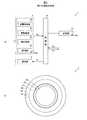
図1(a)は、操作装置の一例を示す概略図であり、図1(b)は、操作装置のダイヤル周辺の断面の一例を示し、図1(c)は、被検出部周辺の一例を拡大した概略図である。図2(a)は、操作装置のブロック図の一例であり、図2(b)は、操作装置の下面図の一例である。なお、以下に記載する実施の形態に係る各図において、図形間の比率は、実際の比率とは異なる場合がある。また図2(a)では、主な信号や情報の流れを矢印で示している。[First Embodiment]
(Outline of operation device 1)
1 (a) is a schematic view showing an example of an operating device, FIG. 1 (b) shows an example of a cross section around the dial of the operating device, and FIG. 1 (c) shows an example of the periphery of the detected portion. It is an enlarged schematic view. FIG. 2A is an example of a block diagram of the operating device, and FIG. 2B is an example of a bottom view of the operating device. In each figure according to the embodiment described below, the ratio between the figures may differ from the actual ratio. Further, in FIG. 2A, the main signal and information flow are indicated by arrows.
操作装置1は、例えば、車両に配置されている。操作装置1は、車両に搭載された空調装置、ナビゲーション装置、音楽及び映像再生装置、及び車両の自動運転や運転支援、車両の基本設定などを制御する制御装置と電気的に接続されている。本実施の形態では、一例として、操作装置1が空調装置と電気的に接続されている場合について説明する。 The
この操作装置1は、ユーザによる接触操作と操作部を用いた操作との異なる入力方法を受け付けるように構成されている。接触操作とは、ユーザの身体の一部、又は専用のスライラスペンなどがパネル3の表面30に直接接触する、つまりエアギャップが生じない、タッチ操作、タップ操作、なぞり操作及びスワイプ操作などである。以下では、接触操作としてタッチ操作を例にして説明する。 The
操作装置1は、図1(a)〜図1(c)に示すように、表面30に凹部31が形成されたパネル3と、パネル3の裏側に配置され、静電容量を検出する検出部4と、ユーザの操作を受け付ける操作部と、操作部に設けられると共に一部が凹部31内に位置し、ユーザの操作部の把持によってパネル3の表面30より検出部4に近い位置に静電容量を生じさせる導電部材7と、を備えて概略構成されている。 As shown in FIGS. 1 (a) to 1 (c), the
本実施の形態の操作部は、回転操作可能なダイヤル6である。なお操作部は、ダイヤル6に限定されず、一次元方向に移動可能な操作部材を有するスライド操作装置、二次元方向に倒す操作が可能な操作レバーを有するジョイステック装置などであっても良い。 The operation unit of this embodiment is a
操作装置1は、検出部4の裏側に画像を表示する表示部5を備えている。検出部4は、画像を透過する透明電極を有している。ダイヤル6は、画像が透過する透過領域100を有する。従って操作装置1は、ダイヤル6の透過領域100を介して表示部5の画像が表示される。 The
つまり透過領域100は、図1(b)に示すように、表示部5の画像を透過するので、ユーザがダイヤル6の中央に表示される当該画像を視認することができる。本実施の形態の透過領域100は、ダイヤル6の中央に設けられた開口64によって形成されている。なお変形例として透過領域100は、透明な樹脂やガラスを介して表示部5が透過する構成であっても良い。 That is, as shown in FIG. 1B, the
また操作装置1は、パネル3、検出部4及び表示部5によってタッチパネル2が形成されている。このタッチパネル2は、パネル3の表面30に対するタッチ操作などの接触操作を受け付けると共に、表示部5によって画像が表示される。そして操作装置1は、タッチパネル2を制御する制御部10を備えている。 Further, in the
(タッチパネル2の構成)
タッチパネル2は、例えば、車両のセンターコンソールなどに配置される。パネル3は、ポリカーボネートなどの透明な樹脂材料を用いて板状に形成されている。このパネル3には、凹部31が形成されている。この凹部31は、ダイヤル6の形状に合わせて外形が円形となっている。図1(c)に示すように、表面30から検出部4までの距離がL1であり、凹部31の底面32から検出部4までの距離がL1より短いL2である。(Structure of touch panel 2)
The
検出部4は、図2(a)に示すように、静電制御部40と、複数の駆動電極41と、複数の検出電極42と、記憶部43と、を備えて概略構成されている。駆動電極41と検出電極42は、ITO(スズドープ酸化インジウム:Indium Tin Oxide)などの透明電極である。 As shown in FIG. 2A, the detection unit 4 is roughly configured to include an
静電制御部40は、例えば、記憶されたプログラムに従って、取得したデータに演算、加工などを行うCPU(Central Processing Unit)、半導体メモリであるRAM(Random Access Memory)及びROM(Read Only Memory)などから構成されるマイクロコンピュータである。このROMには、例えば、静電制御部40が動作するためのプログラムが格納されている。RAMは、例えば、一時的に演算結果などを格納する記憶領域として用いられる。また静電制御部40は、その内部にクロック信号を生成する手段を有し、このクロック信号に基づいて動作を行う。 The
静電制御部40は、駆動電極41と検出電極42との接続を切り替えて全ての組み合わせで静電容量を読み出し、検出対象を検出した検出点の座標を含む検出情報S1を制御部10に出力するように構成されている。
静電制御部40は、記憶部43に記憶された静電しきい値430に基づいて操作を検出する。この記憶部43は、静電制御部40と同じ基板に設けられた半導体メモリであるがこれに限定されない。 The
静電制御部40は、静電しきい値430を超えた静電容量が存在する場合、検出対象を検出したと判定する。この検出対象は、ユーザの操作指9やダイヤル6に設けられた導電部材7である。 When the electrostatic capacity exceeding the
タッチパネル2は、図1(a)に示すように、左上を原点として直交座標系であるXY座標系が設定されている。静電制御部40は、XY座標における検出点を算出する。この検出点は、例えば、加重平均を用いて算出されるがこれに限定されず、重心の座標として算出されても良いし、他の方法で算出されても良い。 As shown in FIG. 1A, the
表示部5は、液晶ディスプレイや有機EL(Electro-Luminescence)ディスプレイである。表示部5は、操作装置1が接続された電子機器から出力される表示情報S2に基づいて画像を表示する。The display unit 5 is a liquid crystal display or an organic EL (Electro-Luminescence) display. Display unit 5 displays an image based on the display information S2 of the
図1(a)に示すタッチパネル2の表示画面20には、一例として、温度を示す画像21、複数のアイコン22と、ダイヤル6の透過領域100に表示される透過画像23と、が表示される。 As an example, the
画像21は、ダイヤル6の回転操作によって増加又は減少する設定温度を示している。ユーザがダイヤル6を時計回り、つまり矢印A方向に回転させると、設定温度が増加する。またユーザがダイヤル6を反時計回り、つまり矢印B方向に回転させると、設定温度が減少する。
アイコン22は、空調装置の機能を示している。ユーザは、パネル3に対して所望のアイコン22にタッチ操作を行うことにより、機能を選択することができる。図1(a)では、選択されたアイコン22に対して斜線が付されている。そしてタッチパネル2は、ダイヤル6によって操作される機能を透過領域100に透過画像23として表示する。 The
(ダイヤル6の構成)
ダイヤル6は、略円柱形状を有している。このダイヤル6は、図1(a)及び図1(b)に示すように、外形が円形状となる透過領域100を中央に有している。このダイヤル6は、パネル3の凹部31に配置されている。(Configuration of dial 6)
The
ダイヤル6は、図1(b)に示すように、本体60と、回転支持部67と、を備えている。本体60は、例えば、ABS(Acrylonitrile Butadiene Styrene)樹脂などの樹脂材料を用いて形成されている。なお変形例として、本体60は、導電部材で形成されても良い。 As shown in FIG. 1B, the
ダイヤル6は、中に内部空間600を有すると共に、側面63が上面61に向かって傾斜する形状を有している。この本体60は、上面61の中央に開口64を有している。この開口64は、上面61から下面62に向かって狭まる形状を有している。そして開口64の下面62には、パネル3及び検出部4を介して表示部5が露出している。この露出した領域が透過領域100となっている。 The
本体60の下面62には、挿入開口65が設けられている。この挿入開口65には、回転支持部67が挿入される。この挿入開口65は、本体60の内部空間600と繋がり、中央側に嵌合部66が設けられている。この嵌合部66は、本体60の内部空間600に、リング状の溝として設けられている。 An
回転支持部67は、両面テープ8を介してパネル3の凹部31の底面32に取り付けられている。本体60は、回転支持部67に支持されながら矢印A方向及び矢印B方向に回転する。この両面テープ8は、ダイヤル6の取り外しが容易に行えるように、シリコーンなどの粘着性の高い粘着剤を備えて構成されても良い。また回転支持部67の取り付けは、両面テープ8ではなく、車両の振動などで外れないように、接着剤で行われても良い。 The
回転支持部67は、外形が円形状である。この回転支持部67は、中央側に爪部68を有している。この爪部68は、本体60の嵌合部66と嵌め合い、本体60と回転支持部67とを回転可能に一体としている。 The
(導電部材7の構成)
導電部材7は、少なくともダイヤル6の側面63及び下面62に設けられている。導電部材7は、ダイヤル6に塗布された導電性塗料である。導電性塗料は、例えば、アクリル樹脂やポリエステル樹脂などにカーボン粒子を混合した塗料であるがこれに限定されない。(Structure of Conductive Member 7)
The
導電部材7は、図1(b)に示すように、下面62、側面63、上面61、及び開口64の内面64aに形成されている。ユーザがダイヤル6に接触すると、下面62と検出部4との間に静電容量が生じる。この下面62には、導電部材7と電気的に接続する被検出部70が設けられている。なお導電部材7は、ダイヤル6を把持した際、ユーザの手が導電部材7に接触して下面62の被検出部70と導通すれば良いので、側面63などに部分的に設けられても良い。 As shown in FIG. 1B, the
検出部4は、この被検出部70をユーザの操作指9の代わりに検出する。ダイヤル6の操作によって、被検出部70が移動する。検出部4は、被検出部70の移動を検出することでダイヤル6の操作位置を検出する。 The detection unit 4 detects the detected
被検出部70は、導電部材7の一部として形成されても良いし、導電部材7と別にネジや導電性接着剤などにより、ダイヤル6に取り付けられたものであっても良い。本実施の形態の被検出部70は、導電部材7の一部として塗布によって形成されたものである。 The detected
以下では、タッチ操作の検出感度と、ダイヤル6の検出感度と、について説明する。図1(c)の紙面左側に点線で示すコンデンサは、パネル3の表面30に対するタッチ操作によって生じる静電容量C1を有するコンデンサを示している。また図1(c)の紙面右側に点線で示すコンデンサは、ダイヤル6に対する把持によって生じる合成静電容量C4を有するコンデンサを示している。Hereinafter, the detection sensitivity of the touch operation and the detection sensitivity of the
(検出感度について)
検出部4は、静電容量に基づいて操作を検出する。一般的に静電容量Cは、誘電率ε、電極間の距離L、及び面積Sを用いて以下の式(1)によって表される。
C=ε×(S/L)・・・(1)
タッチ操作の検出とダイヤル6の操作位置の検出において、検出感度の差を小さく、つまり静電しきい値430を切り替えずに検出するためには、エアギャップのない操作指9によるタッチ操作によって検出される静電容量C1と、エアギャップが生じるダイヤル6のダイヤル操作によって検出される合成静電容量C4と、の差が小さければ良い。(About detection sensitivity)
The detection unit 4 detects the operation based on the capacitance. Generally, the capacitance C is represented by the following equation (1) using the dielectric constant ε, the distance L between the electrodes, and the area S.
C = ε × (S / L) ・ ・ ・ (1)
In order to reduce the difference in detection sensitivity between the touch operation detection and the
従ってパネル3は、表面30から検出部4までの静電容量C1と、導電部材7から凹部31の底面32までの静電容量C2、及び底面32から検出部4までの静電容量C3の合成静電容量C4と、の差を小さくする深さの凹部31を有する。Therefore, the panel 3 has a capacitance C 1 from the
なお静電容量C2における導電部材7は、検出部4と対向する被検出部70である。またユーザがダイヤル6を把持した場合、ダイヤル6に接触する面積は、大きくなるが検出部4と対向する面積が増える訳ではないので、合成静電容量C4の算出には、被検出部70の面積を使用する。The
静電容量C1は、表面30から検出部4までの距離L1、操作指9の接触面積Sa、及びパネル3の誘電率をε1として式(1)を参照すると、以下の式(2)となる。
C1=ε1×(Sa/L1)・・・(2)The capacitance C1 is calculated by referring to the following equation (1) withthe distance L 1 from the
C1 = ε1 × (Sa / L1 ) ・ ・ ・ (2)
また静電容量C2は、被検出部70から凹部31の底面32までの距離L3、被検出部70の面積Sb、及び真空の誘電率ε0として式(1)を参照すると、以下の式(3)となる。
C2=ε0×(Sb/L3)・・・(3)Further, the capacitance C2is the distance L 3 from the detected
C2 = ε0 × (Sb / L3 ) ・ ・ ・ (3)
さらに静電容量C3は、底面32から検出部4までの距離L2、被検出部70の面積Sb、及びパネル3の誘電率をε1として式(1)を参照すると、以下の式(4)となる。
C3=ε1×(Sb/L2)・・・(4)Further, the capacitance C3 is calculated by referring to the following equation,where the distance L 2 from the
C3 = ε1 × (Sb / L2 ) ・ ・ ・ (4)
合成静電容量C4は、静電容量C2及び静電容量C3を用いると以下の式(5)となる。
1/C4=(1/C2)+(1/C3)・・・(5)The combined capacitance C4 is given by the following equation (5) when thecapacitance C 2 and the capacitance C3 are used.
1 / C4 = (1 / C2 ) + (1 / C3 ) ... (5)
以上より、タッチ操作の静電容量C1と合成静電容量C4とが以下の式(6)を満たせば、静電しきい値430を切り替えなくても検出感度の違いを抑制することができる。
C1=C4・・・(6)From the above, if the capacitance C1 of the touch operation and the combined capacitance C4 satisfy the following equation (6), the difference in detection sensitivity can be suppressed without switching the
C1 = C4 ... (6)
ここでパネル3がポリカーボネートである場合、誘電率ε1は、真空の誘電率ε0のおよそ3倍程度であるので、計算を簡単にするため、ε0を1、ε1を3として式(2)〜式(5)を用いて式(6)を計算してまとめると、以下の式(7)となる。
3Sa/L1=3Sb/(L2+3L3)・・・(7)Here, when the panel 3 is made of polycarbonate, the permittivity ε1 is about three times the permittivity ε0 of the vacuum. Therefore, in order to simplify the calculation, theequation (ε 0 is 1 and ε1 is 3). When the equation (6) is calculated and summarized using the equations (2) to (5), the following equation (7) is obtained.
3Sa / L1 = 3Sb / (L2 + 3L3 ) ... (7)
タッチ操作の際の操作指9の接触面積Saと被検出部70の面積Sbとが等しいとして式(7)を整理すると、以下の式(8)となる。
L1=L2+3L3・・・(8)
例えば、凹部31の深さをL1/2(=L2)とした場合、距離L3は、L1/6となる。また例えば、凹部31の深さをL1/3(=L2)とした場合、距離L3は、2L1/9となる。操作装置1は、この深さの凹部31にダイヤル6を配置することで、タッチ操作とダイヤル操作とで検出感度の差が抑制される。If the equation (7) is arranged assuming that the contact area S aof the operating finger 9 and the area S b of the detected
L1 = L2 + 3L3 ... (8)
For example, if the depth of the
(制御部10の構成)
制御部10は、例えば、記憶されたプログラムに従って、取得したデータに演算、加工などを行うCPU、半導体メモリであるRAM及びROMなどから構成されるマイクロコンピュータである。このROMには、例えば、制御部10が動作するためのプログラムが格納されている。RAMは、例えば、一時的に演算結果などを格納する記憶領域として用いられる。また制御部10は、その内部にクロック信号を生成する手段を有し、このクロック信号に基づいて動作を行う。(Structure of control unit 10)
The
制御部10は、記憶部12と電気的に接続されている。この記憶部12は、制御部10と同じ基板に設けられた半導体メモリであるがこれに限定されない。記憶部12には、検出領域情報120が記憶されている。 The
制御部10は、被検出部70が検出される検出領域101の情報である検出領域情報120を有している。制御部10は、検出部4が検出した検出点が凹部31の検出領域101に位置した場合、ダイヤル6の操作として操作情報S3を接続された電子機器に出力する。この検出領域101は、ダイヤル操作に伴って被検出部70が移動するリング形の軌跡の領域であっても良いし、凹部31に対応した円形の領域であっても良い。The
制御部10は、タッチ操作が検出された場合、タッチ操作に応じた操作情報S3を生成して接続された電子機器に出力する。タッチ操作に応じた操作情報S3とは、例えば、検出点の座標に関する情報である。
また制御部10は、ダイヤル操作が検出された場合、ダイヤル操作に応じた操作情報S3を生成して接続された電子機器に出力する。ダイヤル操作に応じた操作情報S3とは、例えば、ダイヤル6の回転角に関する情報である。The
以下では、本実施の形態の操作装置1の動作について図3のフローチャートに従って説明する。 Hereinafter, the operation of the
(動作)
操作装置1の制御部10は、周期的に検出情報S1を取得する。制御部10は、ステップ1の「Yes」が成立する、つまり操作が検出された場合(Step1:Yes)、検出領域情報120に基づいて検出点がどの領域に検出されたかにより、タッチ操作かダイヤル操作かを判定する。(motion)
制御部10は、なされた操作がタッチ操作であった場合(Step2:Yes)、タッチ操作に応じた操作情報S3を生成して接続された電子機器に出力する(Step3)。
ここでステップ2において制御部10は、なされた操作がダイヤル操作であった場合(Step2:No)、ダイヤル操作に応じた操作情報S3を生成して接続された電子機器に出力する(Step4)。Here, the
(第1の実施の形態の効果)
本実施の形態に係る操作装置1は、入力方法の違いによる検出感度の差を抑制することができる。操作装置1は、ダイヤル操作では、パネル3との間にエアギャップが生じるため、パネル3の表面30にダイヤル6を配置すると、タッチ操作とダイヤル操作とで検出感度に差が生じる。本実施の形態の操作装置1は、ダイヤル6を凹部31に配置して被検出部70と検出部4との距離を小さくし、エアギャップによる検出感度の低下を補うので、ダイヤルをパネルの表面に配置する場合と比べて、タッチ操作とダイヤル操作の入力方法の違いによる検出感度の差を抑制することができる。(Effect of the first embodiment)
The operating
操作装置1は、ダイヤル操作の際、検出感度の低下を補うため、検出感度を高くする必要がないので、検出感度を高くする場合と比べて、外来ノイズに対する耐性が高い。 Since the
操作装置1は、ダイヤル6の中央に表示部5の表示が透過する透過領域100を有しているので、この構成を採用しない場合と比べて、ユーザにとってダイヤル6によって操作可能な機能や設定値などが認識し易く、操作性が向上する。 Since the
[第2の実施の形態]
第2の実施の形態は、ダイヤルの被検出部がパネルの凹部内に位置する点で他の実施の形態と異なっている。[Second Embodiment]
The second embodiment is different from the other embodiments in that the detected portion of the dial is located in the recess of the panel.
図4(a)は、操作装置の断面図の一例であり、図4(b)は、パネルに設けられた凹部の一例を示す概略図であり、図4(c)は、パネルに設けられた凹部の変形例の一例である。なお以下に記載する実施の形態において、第1の実施の形態と同じ機能及び構成を有する部分は、第1の実施の形態と同じ符号を付し、その説明は省略するものとする。 FIG. 4A is an example of a cross-sectional view of the operating device, FIG. 4B is a schematic view showing an example of a recess provided in the panel, and FIG. 4C is provided in the panel. This is an example of deformation of the concave portion. In the embodiments described below, parts having the same functions and configurations as those of the first embodiment are designated by the same reference numerals as those of the first embodiment, and the description thereof will be omitted.
本実施の形態の操作装置1の導電部材7は、図4(a)及び図4(b)に示すように、ダイヤル6の下面62からパネル3に向かって突出する突出部としての被検出部70を備えている。また凹部31は、ダイヤル6に対する操作による被検出部70の軌跡に沿って形成されている。そして被検出部70は、凹部31に挿入されている。 As shown in FIGS. 4A and 4B, the
第1の実施の形態では、ダイヤル6が凹部31内に配置された。本実施の形態のダイヤル6は、導電部材7の一部である被検出部70が凹部31に挿入されている。 In the first embodiment, the
凹部31は、図4(b)に示すように、ダイヤル6の回転に応じて被検出部70の軌跡となる円状の溝として形成されている。被検出部70は、この溝の中を移動するため、一例として、円柱形状を有している。 As shown in FIG. 4B, the
なお変形例として凹部31は、図4(c)に示すように、部分的なリング状の溝として形成されても良い。この場合、ダイヤル6は、凹部31によって規定される回転角で回転する。また他の変形例としてダイヤル6が複数の被検出部70を有し、複数の被検出部70に応じて部分的なリング状の複数の溝として形成されても良い。 As a modification, the
(第2の実施の形態の効果)
本実施の形態の操作装置1は、パネル3に大きな凹部31を設けなくても良いので、この構成を採用しない場合と比べて、パネル3の薄い部分が少なくなり、割れなどを抑制することができる。(Effect of the second embodiment)
Since the
ここで他の実施の形態としての操作装置1は、操作部が交換可能に構成されている。操作部は、操作可能な機能ごとに用意される。操作部は、機能ごとに形状が異なる被検出部を有する。制御部10は、被検出部の形状から操作部の機能を判定し、検出された操作部の操作に応じて操作情報S3を生成して出力する。Here, in the
以上述べた少なくとも1つの実施の形態の操作装置1によれば、入力方法の違いによる検出感度の差を抑制することが可能となる。 According to the
以上、本発明のいくつかの実施の形態及び変形例を説明したが、これらの実施の形態及び変形例は、一例に過ぎず、特許請求の範囲に係る発明を限定するものではない。これら新規な実施の形態及び変形例は、その他の様々な形態で実施されることが可能であり、本発明の要旨を逸脱しない範囲で、種々の省略、置き換え、変更などを行うことができる。また、これら実施の形態及び変形例の中で説明した特徴の組合せの全てが発明の課題を解決するための手段に必須であるとは限らない。さらに、これら実施の形態及び変形例は、発明の範囲及び要旨に含まれると共に、特許請求の範囲に記載された発明とその均等の範囲に含まれる。 Although some embodiments and modifications of the present invention have been described above, these embodiments and modifications are merely examples and do not limit the invention according to the claims. These novel embodiments and modifications can be implemented in various other embodiments, and various omissions, replacements, changes, etc. can be made without departing from the gist of the present invention. Moreover, not all combinations of features described in these embodiments and modifications are essential as means for solving the problems of the invention. Further, these embodiments and modifications are included in the scope and gist of the invention, and are included in the scope of the invention described in the claims and the equivalent scope thereof.
1…操作装置、2…タッチパネル、3…パネル、4…検出部、5…表示部、6…ダイヤル、7…導電部材、8…両面テープ、9…操作指、10…制御部、12…記憶部、20…表示画面、21…画像、22…アイコン、23…透過画像、30…表面、31…凹部、32…底面、40…静電制御部、41…駆動電極、42…検出電極、43…記憶部、60…本体、61…上面、62…下面、63…側面、64…開口、64a…内面、65…挿入開口、66…嵌合部、67…回転支持部、68…爪部、70…被検出部、100…透過領域、101…検出領域、120…検出領域情報、430…静電しきい値、600…内部空間1 ... Operation device, 2 ... Touch panel, 3 ... Panel, 4 ... Detection unit, 5 ... Display unit, 6 ... Dial, 7 ... Conductive member, 8 ... Double-sided tape, 9 ... Operation finger, 10 ... Control unit, 12 ... Memory Unit, 20 ... Display screen, 21 ... Image, 22 ... Icon, 23 ... Transparent image, 30 ... Surface, 31 ... Recessed, 32 ... Bottom, 40 ... Electrostatic control unit, 41 ... Drive electrode, 42 ... Detection electrode, 43 ... storage unit, 60 ... main body, 61 ... upper surface, 62 ... lower surface, 63 ... side surface, 64 ... opening, 64a ... inner surface, 65 ... insertion opening, 66 ... fitting part, 67 ... rotation support part, 68 ... claw part, 70 ... Detected part, 100 ... transmission area, 101 ... detection area, 120 ... detection area information, 430 ... electrostatic threshold value, 600 ... internal space
Claims (7)
Translated fromJapanese前記パネルの裏側に配置され、静電容量を検出する検出部と、
ユーザの操作を受け付ける操作部と、
前記操作部に設けられると共に一部が前記凹部内に位置し、ユーザの前記操作部の把持によって前記パネルの前記表面より前記検出部に近い位置に静電容量を生じさせる導電部材と、
を備えた操作装置。A panel with recesses on the surface and
A detector located on the back side of the panel to detect capacitance,
An operation unit that accepts user operations and
A conductive member provided in the operation portion and a part of which is located in the recess, and a capacitance is generated at a position closer to the detection portion than the surface of the panel by grasping the operation portion by the user.
An operating device equipped with.
請求項1に記載の操作装置。The conductive member is provided at least on the side surface and the lower surface of the operation portion.
The operating device according to claim 1.
前記検出部は、前記画像を透過する透明電極を有し、
前記操作部は、前記画像が透過する透過領域を有する、
請求項1又は2に記載の操作装置。A display unit for displaying an image is provided on the back side of the detection unit.
The detection unit has a transparent electrode that transmits the image.
The operation unit has a transparent region through which the image is transmitted.
The operating device according to claim 1 or 2.
請求項1乃至3のいずれか1項に記載の操作装置。The operation unit is arranged in the recess of the panel.
The operating device according to any one of claims 1 to 3.
前記凹部は、前記操作部に対する操作による前記突出部の軌跡に沿って形成され、
前記突出部は、前記凹部に挿入される、
請求項1乃至4のいずれか1項に記載の操作装置。The conductive member has a protruding portion that protrudes from the lower surface of the operating portion toward the panel.
The recess is formed along the locus of the protrusion by operating the operation portion.
The protrusion is inserted into the recess.
The operating device according to any one of claims 1 to 4.
請求項1乃至5のいずれか1項に記載の操作装置。The conductive member is a conductive paint applied to the operation portion.
The operating device according to any one of claims 1 to 5.
請求項1乃至6のいずれか1項に記載の操作装置。The panel has a combined capacitance of the capacitance from the surface to the detection unit, the capacitance from the conductive member to the bottom surface of the recess, and the capacitance from the bottom surface to the detection unit. With the recesses of a depth that reduces the difference between
The operating device according to any one of claims 1 to 6.
Priority Applications (1)
| Application Number | Priority Date | Filing Date | Title |
|---|---|---|---|
| JP2019199643AJP2021072020A (en) | 2019-11-01 | 2019-11-01 | Operational device |
Applications Claiming Priority (1)
| Application Number | Priority Date | Filing Date | Title |
|---|---|---|---|
| JP2019199643AJP2021072020A (en) | 2019-11-01 | 2019-11-01 | Operational device |
Publications (1)
| Publication Number | Publication Date |
|---|---|
| JP2021072020Atrue JP2021072020A (en) | 2021-05-06 |
Family
ID=75713166
Family Applications (1)
| Application Number | Title | Priority Date | Filing Date |
|---|---|---|---|
| JP2019199643APendingJP2021072020A (en) | 2019-11-01 | 2019-11-01 | Operational device |
Country Status (1)
| Country | Link |
|---|---|
| JP (1) | JP2021072020A (en) |
Citations (6)
| Publication number | Priority date | Publication date | Assignee | Title |
|---|---|---|---|---|
| JP2000172439A (en)* | 1998-11-27 | 2000-06-23 | Internatl Business Mach Corp <Ibm> | Device and method for assisting scroll for computer |
| JP2012226554A (en)* | 2011-04-19 | 2012-11-15 | Wacom Co Ltd | Cordless position indicator |
| WO2015174092A1 (en)* | 2014-05-15 | 2015-11-19 | パナソニックIpマネジメント株式会社 | Operation knob and display device in which same is used |
| JP2018081396A (en)* | 2016-11-15 | 2018-05-24 | 信行 千葉 | Input device |
| WO2018109835A1 (en)* | 2016-12-13 | 2018-06-21 | 三菱電機株式会社 | Mechanical knob, touch-panel-equipped display device, and device and method for controlling touch panel |
| WO2019098055A1 (en)* | 2017-11-20 | 2019-05-23 | パナソニックIpマネジメント株式会社 | Input device |
- 2019
- 2019-11-01JPJP2019199643Apatent/JP2021072020A/enactivePending
Patent Citations (6)
| Publication number | Priority date | Publication date | Assignee | Title |
|---|---|---|---|---|
| JP2000172439A (en)* | 1998-11-27 | 2000-06-23 | Internatl Business Mach Corp <Ibm> | Device and method for assisting scroll for computer |
| JP2012226554A (en)* | 2011-04-19 | 2012-11-15 | Wacom Co Ltd | Cordless position indicator |
| WO2015174092A1 (en)* | 2014-05-15 | 2015-11-19 | パナソニックIpマネジメント株式会社 | Operation knob and display device in which same is used |
| JP2018081396A (en)* | 2016-11-15 | 2018-05-24 | 信行 千葉 | Input device |
| WO2018109835A1 (en)* | 2016-12-13 | 2018-06-21 | 三菱電機株式会社 | Mechanical knob, touch-panel-equipped display device, and device and method for controlling touch panel |
| WO2019098055A1 (en)* | 2017-11-20 | 2019-05-23 | パナソニックIpマネジメント株式会社 | Input device |
Similar Documents
| Publication | Publication Date | Title |
|---|---|---|
| US7796124B2 (en) | Input device and electronic apparatus | |
| JP6618122B2 (en) | Input device and touch panel control method | |
| US8570290B2 (en) | Image display device | |
| US7825797B2 (en) | Proximity sensor device and method with adjustment selection tabs | |
| US10088964B2 (en) | Display device and electronic equipment | |
| US6924752B2 (en) | Three-dimensional contact-sensitive feature for electronic devices | |
| KR101149980B1 (en) | Touch sensor for a display screen of an electronic device | |
| US20100271301A1 (en) | Input processing device | |
| EP2835722A1 (en) | Input device | |
| CN104915134A (en) | Vehicle operation apparatus | |
| US20110134077A1 (en) | Input Device and Input Method | |
| JP2017058718A (en) | Operation detection device | |
| WO2018008492A1 (en) | Touch panel control device and electronic device | |
| US20130300709A1 (en) | Information processing device and input device | |
| TW202321881A (en) | System and method of adjusting cursor speed | |
| EP2835721A1 (en) | Input device | |
| EP4354264A1 (en) | Input display device | |
| JP2021072020A (en) | Operational device | |
| JP7269154B2 (en) | Operating device and calculation method | |
| JP2013073365A (en) | Information processing device | |
| JP2024087947A (en) | Input display device | |
| US20180292924A1 (en) | Input processing apparatus | |
| US12422255B2 (en) | Tilt determination | |
| JP2016218820A (en) | Operation detection device | |
| JP2024081202A (en) | Input display device |
Legal Events
| Date | Code | Title | Description |
|---|---|---|---|
| A621 | Written request for application examination | Free format text:JAPANESE INTERMEDIATE CODE: A621 Effective date:20220527 | |
| A977 | Report on retrieval | Free format text:JAPANESE INTERMEDIATE CODE: A971007 Effective date:20230227 | |
| A131 | Notification of reasons for refusal | Free format text:JAPANESE INTERMEDIATE CODE: A131 Effective date:20230404 | |
| A02 | Decision of refusal | Free format text:JAPANESE INTERMEDIATE CODE: A02 Effective date:20231003 |