JP2021031336A - SiC CHEMICAL VAPOR DEPOSITION APPARATUS - Google Patents
SiC CHEMICAL VAPOR DEPOSITION APPARATUSDownload PDFInfo
- Publication number
- JP2021031336A JP2021031336AJP2019153706AJP2019153706AJP2021031336AJP 2021031336 AJP2021031336 AJP 2021031336AJP 2019153706 AJP2019153706 AJP 2019153706AJP 2019153706 AJP2019153706 AJP 2019153706AJP 2021031336 AJP2021031336 AJP 2021031336A
- Authority
- JP
- Japan
- Prior art keywords
- raw material
- material gas
- containing raw
- sic
- gas introduction
- Prior art date
- Legal status (The legal status is an assumption and is not a legal conclusion. Google has not performed a legal analysis and makes no representation as to the accuracy of the status listed.)
- Pending
Links
- 238000005229chemical vapour depositionMethods0.000titleclaimsabstractdescription27
- 239000002994raw materialSubstances0.000claimsabstractdescription138
- 229910052799carbonInorganic materials0.000claimsdescription9
- 230000015572biosynthetic processEffects0.000claimsdescription8
- OKTJSMMVPCPJKN-UHFFFAOYSA-NCarbonChemical compound[C]OKTJSMMVPCPJKN-UHFFFAOYSA-N0.000claimsdescription7
- 238000004519manufacturing processMethods0.000abstractdescription11
- 238000000151depositionMethods0.000abstract1
- 230000008021depositionEffects0.000abstract1
- 230000007774longtermEffects0.000abstract1
- 239000007789gasSubstances0.000description186
- HBMJWWWQQXIZIP-UHFFFAOYSA-Nsilicon carbideChemical compound[Si+]#[C-]HBMJWWWQQXIZIP-UHFFFAOYSA-N0.000description117
- 229910010271silicon carbideInorganic materials0.000description116
- 235000012431wafersNutrition0.000description58
- 239000000203mixtureSubstances0.000description12
- 239000002244precipitateSubstances0.000description11
- 238000010438heat treatmentMethods0.000description10
- 239000000463materialSubstances0.000description9
- 230000000052comparative effectEffects0.000description6
- 229910052751metalInorganic materials0.000description5
- 239000002184metalSubstances0.000description5
- 239000000919ceramicSubstances0.000description4
- 239000004065semiconductorSubstances0.000description4
- 239000012159carrier gasSubstances0.000description3
- 239000000460chlorineSubstances0.000description3
- 230000007423decreaseEffects0.000description3
- 239000012535impuritySubstances0.000description3
- 238000001556precipitationMethods0.000description3
- 229910052710siliconInorganic materials0.000description3
- QGZKDVFQNNGYKY-UHFFFAOYSA-NAmmoniaChemical compoundNQGZKDVFQNNGYKY-UHFFFAOYSA-N0.000description2
- PAYRUJLWNCNPSJ-UHFFFAOYSA-NAnilineChemical compoundNC1=CC=CC=C1PAYRUJLWNCNPSJ-UHFFFAOYSA-N0.000description2
- ROSDSFDQCJNGOL-UHFFFAOYSA-NDimethylamineChemical compoundCNCROSDSFDQCJNGOL-UHFFFAOYSA-N0.000description2
- OAKJQQAXSVQMHS-UHFFFAOYSA-NHydrazineChemical compoundNNOAKJQQAXSVQMHS-UHFFFAOYSA-N0.000description2
- BAVYZALUXZFZLV-UHFFFAOYSA-NMethylamineChemical compoundNCBAVYZALUXZFZLV-UHFFFAOYSA-N0.000description2
- ATUOYWHBWRKTHZ-UHFFFAOYSA-NPropaneChemical compoundCCCATUOYWHBWRKTHZ-UHFFFAOYSA-N0.000description2
- BLRPTPMANUNPDV-UHFFFAOYSA-NSilaneChemical compound[SiH4]BLRPTPMANUNPDV-UHFFFAOYSA-N0.000description2
- 238000009792diffusion processMethods0.000description2
- 238000005530etchingMethods0.000description2
- 238000005259measurementMethods0.000description2
- 150000002739metalsChemical class0.000description2
- 238000012986modificationMethods0.000description2
- 230000004048modificationEffects0.000description2
- 229910052750molybdenumInorganic materials0.000description2
- 230000002093peripheral effectEffects0.000description2
- 238000010926purgeMethods0.000description2
- 230000005855radiationEffects0.000description2
- 229910000077silaneInorganic materials0.000description2
- 239000007787solidSubstances0.000description2
- 229910052715tantalumInorganic materials0.000description2
- JLTRXTDYQLMHGR-UHFFFAOYSA-NtrimethylaluminiumChemical compoundC[Al](C)CJLTRXTDYQLMHGR-UHFFFAOYSA-N0.000description2
- GETQZCLCWQTVFV-UHFFFAOYSA-NtrimethylamineChemical compoundCN(C)CGETQZCLCWQTVFV-UHFFFAOYSA-N0.000description2
- 229910052721tungstenInorganic materials0.000description2
- DIIIISSCIXVANO-UHFFFAOYSA-N1,2-DimethylhydrazineChemical compoundCNNCDIIIISSCIXVANO-UHFFFAOYSA-N0.000description1
- VEXZGXHMUGYJMC-UHFFFAOYSA-MChloride anionChemical compound[Cl-]VEXZGXHMUGYJMC-UHFFFAOYSA-M0.000description1
- ZAMOUSCENKQFHK-UHFFFAOYSA-NChlorine atomChemical compound[Cl]ZAMOUSCENKQFHK-UHFFFAOYSA-N0.000description1
- VEXZGXHMUGYJMC-UHFFFAOYSA-NHydrochloric acidChemical compoundClVEXZGXHMUGYJMC-UHFFFAOYSA-N0.000description1
- 229910003902SiCl 4Inorganic materials0.000description1
- XUIMIQQOPSSXEZ-UHFFFAOYSA-NSiliconChemical compound[Si]XUIMIQQOPSSXEZ-UHFFFAOYSA-N0.000description1
- 150000001412aminesChemical class0.000description1
- 229910021529ammoniaInorganic materials0.000description1
- 230000015556catabolic processEffects0.000description1
- 229910052801chlorineInorganic materials0.000description1
- SLLGVCUQYRMELA-UHFFFAOYSA-NchlorosiliconChemical compoundCl[Si]SLLGVCUQYRMELA-UHFFFAOYSA-N0.000description1
- 239000013078crystalSubstances0.000description1
- 238000000354decomposition reactionMethods0.000description1
- 238000007599dischargingMethods0.000description1
- 230000000694effectsEffects0.000description1
- 230000005684electric fieldEffects0.000description1
- 238000011156evaluationMethods0.000description1
- -1for exampleSubstances0.000description1
- 239000011261inert gasSubstances0.000description1
- 238000009434installationMethods0.000description1
- 230000001788irregularEffects0.000description1
- 238000012423maintenanceMethods0.000description1
- 239000002245particleSubstances0.000description1
- 238000012545processingMethods0.000description1
- 239000001294propaneSubstances0.000description1
- 239000010703siliconSubstances0.000description1
- 229910001220stainless steelInorganic materials0.000description1
- 239000010935stainless steelSubstances0.000description1
- 238000005092sublimation methodMethods0.000description1
- 239000000758substrateSubstances0.000description1
Images
Landscapes
- Chemical Vapour Deposition (AREA)
- Recrystallisation Techniques (AREA)
- Crystals, And After-Treatments Of Crystals (AREA)
Abstract
Description
Translated fromJapanese本発明は、SiC化学気相成長装置に関する。 The present invention relates to a SiC chemical vapor deposition apparatus.
炭化珪素(SiC)は、シリコン(Si)に比べて絶縁破壊電界が1桁大きく、バンドギャップが3倍大きく、熱伝導率が3倍程度高い等の特性を有する。SiCはこれらの特性を有することから、パワーデバイス、高周波デバイス、高温動作デバイス等への応用が期待されている。このため、近年、上記のような半導体デバイスにSiCエピタキシャルウェハが用いられるようになっている。 Silicon carbide (SiC) has characteristics such as an dielectric breakdown electric field that is an order of magnitude larger, a band gap that is three times larger, and a thermal conductivity that is about three times higher than that of silicon (Si). Since SiC has these characteristics, it is expected to be applied to power devices, high-frequency devices, high-temperature operation devices, and the like. For this reason, in recent years, SiC epitaxial wafers have come to be used for the above-mentioned semiconductor devices.
SiCエピタキシャルウェハは、SiCウェハ(SiC基板)上にSiC半導体デバイスの活性領域となるSiCエピタキシャル膜を成長させることによって製造される。SiCウェハは、昇華法等で作製したSiCのバルク単結晶から加工して得られ、SiCエピタキシャル膜は、化学気相成長(Chemical Vapor Deposition:CVD)装置によって形成される。 The SiC epitaxial wafer is manufactured by growing a SiC epitaxial film which is an active region of a SiC semiconductor device on a SiC wafer (SiC substrate). The SiC wafer is obtained by processing from a bulk single crystal of SiC produced by a sublimation method or the like, and the SiC epitaxial film is formed by a chemical vapor deposition (CVD) apparatus.
このようなSiC化学気相成長装置の一例として、成膜空間を構成する炉体内において、SiCウェハが載置された載置台を裏面より加熱し、SiCウェハ表面に上方から原料ガスを導入してSiCエピタキシャル膜を成膜する装置が知られている。原料ガスとしては、Si原料含有ガスとC原料含有ガスが用いられる。Si原料含有ガスとC原料含有ガスはそれぞれ分離した複数の配管から成膜空間に導入され、SiCウェハの表面上で混合ガスを生成する。 As an example of such a SiC chemical vapor deposition apparatus, a mounting table on which a SiC wafer is placed is heated from the back surface in a furnace body constituting a film formation space, and a raw material gas is introduced from above onto the surface of the SiC wafer. An apparatus for forming a SiC epitaxial film is known. As the raw material gas, a Si raw material-containing gas and a C raw material-containing gas are used. The Si raw material-containing gas and the C raw material-containing gas are introduced into the film forming space from a plurality of separate pipes to generate a mixed gas on the surface of the SiC wafer.
特許文献1には、SiCエピタキシャル膜の成膜時のパーティクル発生の抑制と、膜厚および濃度の面内均一性の両立を図るために、Si原料含有ガスとC原料含有ガスの間に原料ガス以外のガスとなる第3ガスが導入されるようにした構成のSiC半導体成膜装置が記載されている。なお、この特許文献1には、SiC原料含有ガスを供給する供給路の長さを炉体の径方向の中央部よりも外周部において長くなるようして、SiCウェハの表面に供給される原料ガスのC/Si比をSiCウェハの中央部と外周部とで制御することによって、SiCウェハ面内のC/Si比を制御する構成が記載されている。 Patent Document 1 describes a raw material gas between a Si raw material-containing gas and a C raw material-containing gas in order to suppress the generation of particles during film formation of a SiC epitaxial film and to achieve both in-plane uniformity of film thickness and concentration. A SiC semiconductor film forming apparatus having a configuration in which a third gas, which is a gas other than the above, is introduced is described. In Patent Document 1, the raw material supplied to the surface of the SiC wafer is provided so that the length of the supply path for supplying the SiC raw material-containing gas is longer at the outer peripheral portion than at the central portion in the radial direction of the furnace body. A configuration is described in which the C / Si ratio in the surface of the SiC wafer is controlled by controlling the C / Si ratio of the gas at the central portion and the outer peripheral portion of the SiC wafer.
近年の半導体デバイスの微細化や高密度化に伴って、SiCエピタキシャルウェハに対して、さらなる電気特性の向上、特にキャリア濃度の均一性の向上が求められている。しかしながら、本発明の発明者の検討によると、従来のCVD装置を用いてSiCエピタキシャルウェハを製造すると、製造時間の経過と共に、得られるSiCエピタキシャルウェハのキャリア濃度が不均一になりやすいことが判明した。 With the recent miniaturization and high density of semiconductor devices, there is a demand for further improvement of electrical characteristics, particularly improvement of carrier concentration uniformity, for SiC epitaxial wafers. However, according to the study of the inventor of the present invention, it has been found that when a SiC epitaxial wafer is manufactured using a conventional CVD apparatus, the carrier concentration of the obtained SiC epitaxial wafer tends to be non-uniform with the lapse of the manufacturing time. ..
本発明は、前述した事情に鑑みてなされたものであって、その目的は、キャリア濃度の均一性が高いSiCエピタキシャルウェハを長期間にわたって連続的に製造することができるSiC化学気相成長装置を提供することにある。 The present invention has been made in view of the above circumstances, and an object of the present invention is to provide a SiC chemical vapor deposition apparatus capable of continuously producing a SiC epitaxial wafer having high carrier concentration uniformity for a long period of time. To provide.
上記の課題を解決するために、本発明者は検討した結果、SiC化学気相成長装置の炉体内に、2以上のSi含有原料ガス導入管を設けること、そして、2以上のSi含有原料ガス導入管を、Si含有原料ガス導入管の導入口とSiCウェハを載置するための載置台の載置面との距離がそれぞれ異なり、かつその導入口と載置面との距離の最大値と最小値との差が0.6mm以上1.5mm未満となるように配置することが有効であることを見出して、本発明を完成させた。2以上のSi含有原料ガス導入管を上記のように配置することによって、キャリア濃度の均一性が高いSiCエピタキシャルウェハを長期間にわたって連続的に製造することが可能となるのは、SiCウェハの表面上に生成する混合ガスの組成が安定することにより、組成が均一なSiCエピタキシャル膜を成膜することが可能となるためであると考えられる。
すなわち、本発明は、前記の課題を解決するため、以下の手段を提供する。As a result of examination in order to solve the above problems, the present inventor provides two or more Si-containing raw material gas introduction pipes in the furnace body of the SiC chemical vapor deposition apparatus, and two or more Si-containing raw material gas. The distance between the introduction port of the Si-containing raw material gas introduction pipe and the mounting surface of the mounting table for mounting the SiC wafer is different, and the maximum value of the distance between the introduction port and the mounting surface is used. The present invention has been completed by finding that it is effective to arrange the mixture so that the difference from the minimum value is 0.6 mm or more and less than 1.5 mm. By arranging two or more Si-containing raw material gas introduction pipes as described above, it is possible to continuously manufacture a SiC epitaxial wafer having a high uniformity of carrier concentration for a long period of time on the surface of the SiC wafer. It is considered that this is because the stable composition of the mixed gas generated above makes it possible to form a SiC epitaxial film having a uniform composition.
That is, the present invention provides the following means for solving the above-mentioned problems.
[1]成膜空間を構成する炉体と、前記炉体内に備えられ、SiCウェハが載置される載置面を有する載置台と、前記炉体内へSiを含むSi含有原料ガスを導入する2以上のSi含有原料ガス導入管と、前記炉体内へCを含むC含有原料ガスを導入するC含有原料ガス導入管と、を備え、前記2以上の前記Si含有原料ガス導入管は、前記Si含有原料ガス導入管の導入口と前記載置台の前記載置面との距離がそれぞれ異なり、かつ前記導入口と前記載置面との距離の最大値と最小値との差が0.6mm以上1.5mm未満となるように配置されていることを特徴とするSiC化学気相成長装置。[1] A Si-containing raw material gas containing Si is introduced into the furnace body constituting the film formation space, a mounting table provided in the furnace body and having a mounting surface on which a SiC wafer is placed, and the furnace body. The two or more Si-containing raw material gas introduction pipes include two or more Si-containing raw material gas introduction pipes and a C-containing raw material gas introduction pipe for introducing C-containing C-containing raw material gas into the furnace body. The distance between the introduction port of the Si-containing raw material gas introduction pipe and the front-stated mounting surface of the above-mentioned stand is different, and the difference between the maximum value and the minimum value of the distance between the introduction port and the front-stated placement surface is 0.6 mm. A SiC chemical vapor deposition apparatus characterized in that it is arranged so as to be less than 1.5 mm.
[2]前記2以上の前記Si含有原料ガス導入管のうち前記載置台の前記載置面の中心に最も近い位置に配置されているSi含有原料ガス導入管は、前記導入口と前記載置面との距離が最大値を示す前記[1]に記載のSiC化学気相成長装置。[2] Of the two or more Si-containing raw material gas introduction pipes, the Si-containing raw material gas introduction pipes arranged at the positions closest to the center of the front-described mounting surface of the pre-described stand are the introduction port and the pre-described placement. The SiC chemical vapor deposition apparatus according to the above [1], wherein the distance to the surface shows the maximum value.
[3]前記2以上の前記Si含有原料ガス導入管は、それぞれSiCまたはTaCで被覆されたカーボンから形成されている前記[1]または[2]に記載のSiC化学気相成長装置。[3] The SiC chemical vapor deposition apparatus according to the above [1] or [2], wherein the two or more Si-containing raw material gas introduction pipes are formed of carbon coated with SiC or TaC, respectively.
本発明によれば、キャリア濃度の均一性が高いSiCエピタキシャルウェハを長期間にわたって連続的に製造することができるSiC化学気相成長装置を提供することが可能となる。 According to the present invention, it is possible to provide a SiC chemical vapor deposition apparatus capable of continuously producing a SiC epitaxial wafer having high carrier concentration uniformity for a long period of time.
以下、本発明の実施形態に係るSiC化学気相成長装置について、図面を適宜参照しながら詳細に説明する。以下の説明で用いる図面は、本発明の特徴をわかりやすくするために便宜上特徴となる部分を拡大して示している場合があり、各構成要素の寸法比率などは実際とは異なっていることがある。以下の説明において例示される材料、寸法等は一例であって、本発明はそれらに限定されるものではなく、その要旨を変更しない範囲で適宜変更して実施することが可能である。 Hereinafter, the SiC chemical vapor deposition apparatus according to the embodiment of the present invention will be described in detail with reference to the drawings as appropriate. The drawings used in the following description may be enlarged for convenience in order to make the features of the present invention easy to understand, and the dimensional ratios of the respective components may differ from the actual ones. is there. The materials, dimensions, etc. exemplified in the following description are examples, and the present invention is not limited thereto, and the present invention can be appropriately modified without changing the gist thereof.
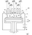
図1は、本発明の一実施形態に係るSiC化学気相成長装置を模式的に説明する模式断面図である。 FIG. 1 is a schematic cross-sectional view schematically illustrating a SiC chemical vapor deposition apparatus according to an embodiment of the present invention.
図1に示すように、本発明の一実施形態に係るSiC化学気相成長装置100は、成膜空間を構成する炉体10と、炉体10内に備えられSiCウェハWを載置する載置台20と、炉体10内へガスを導入するガス導入管とを有する。ガス導入管としては、Siを含むSi含有原料ガスを導入するSi含有原料ガス導入管30と、Cを含むC含有原料ガスを導入するC含有原料ガス導入管31と、原料ガス以外の補助ガスを導入する補助ガス導入管32を備える。また、炉体10はガスを排出するガス排出口40を有する。 As shown in FIG. 1, in the SiC chemical
[炉体]
炉体10は、成膜空間を構成する中空部を有する。SiCエピタキシャル成膜時は、成膜空間の温度は1500℃以上となる。このため、炉体10の材料としては、特に限定されるものではないが、ステンレス等の耐熱性が高い金属が用いられる。[Furnace]
The
[載置台]
載置台20は、SiCウェハWを載置するサセプタ21と、サセプタ21上に載置されたSiCウェハWを加熱する加熱機構22とを有する構成とされている。サセプタ21は、上面にSiCウェハWが載置される載置面21aを有し、内部に加熱機構22が配置される空間を有する。サセプタ21には下方に延びる管状の支持軸が備えられ、この支持軸が図示しない回転機構に連結されることによって、サセプタ21が回転可能とされている。加熱機構22は、SiCウェハWの載置面と対向するヒーターなどによって構成されており、サセプタ21内に設置されている。加熱機構22には、サセプタ21の支持軸内部を通して外部から通電されている。[Mounting stand]
The mounting table 20 is configured to have a
サセプタ21の材料としては、例えば、SiCなどのセラミックス、Ta、Mo、Wなどの金属を用いることができる。また、セラミックスや金属の無垢材の他に、SiCまたはTaC等の炭化金属で被覆されたカーボンを用いることができる。 As the material of the
[ガス導入管]
ガス導入管としては、Si含有原料ガス導入管30と、C含有原料ガス導入管31と、補助ガス導入管32が配置されている。なお、Si含有原料ガス導入管30、C含有原料ガス導入管31および補助ガス導入管32の配置は図1に示すものに限定されるものではない。SiCウェハWの表面上にSiとCと補助ガスを含む均一な混合ガスを生成させることができれば、これらガス導入管の配置は特に制限はなく、不規則であってもよい。ただし、SiCウェハWの表面上に均一な混合ガスを生成させるためには、Si含有原料ガス導入管30、C含有原料ガス導入管31および補助ガス導入管32は、それぞれ2以上配置することが望ましい。[Gas introduction pipe]
As the gas introduction pipe, a Si-containing raw material
(Si含有原料ガス導入管)
Si含有原料ガス導入管30は、Siを含むSi含有原料ガスを炉体10内に導入する。Si含有原料ガスとしては、例えば、シラン系ガスとして、シラン(SiH4)を用いることができる他に、SiH2Cl2、SiHCl3、SiCl4などのエッチング作用があるClを含む塩素系Si原料含有ガス(クロライド系原料)を用いることもできる。(Si-containing raw material gas introduction pipe)
The Si-containing raw material
Si含有原料ガス導入管30は、Si含有原料ガス導入管30の導入口30aと載置台20の載置面21aとの距離H0〜H2がそれぞれ異なるように配置されている。導入口30aと載置面21aとの距離は、H0が最も長く、H1が次に長く、H2が最も短くなっている。導入口30aと載置面21aとの距離の最大値H0と最小値H2との差(H0−H2)は0.6mm以上1.5mm未満とされている。なお、導入口30aと載置面21aとの距離は、導入口30aの中心から垂直方向に載置面21aの表面とを結ぶ線分の長さを意味する。また、導入口30aと載置面21aとの距離が異なるとは、距離の差が0.1mm以上あることを意味する。The Si-containing raw material gas introduction pipe 30 is arranged so that the distances H 0 to H2 between the
Si含有原料ガス導入管30は、SiCエピタキシャル成膜時において、導入口30aの開口周囲にSiCを含む析出物が析出しやすい。また、導入口30aの開口周囲でのSiCを含む析出物の析出量はSi含有原料ガス導入管30の位置によって異なる。これは、輻射熱の大きさがSi含有原料ガス導入管30の位置によって異なることによって、管の位置毎に原料ガスの分解速度および析出物の析出速度が異なるためである。このため、Si含有原料ガス導入管30では、析出物が導入口30aの開口周囲に不均一に堆積することによって、Si含有原料ガス導入管30の長さが不均一に変化し、Si含有原料ガスの導入量が不均一になりやすい傾向がある。そこで、2以上のSi含有原料ガス導入管30を、Si含有原料ガス導入管30と載置台20の載置面21aとの距離がそれぞれ異なるように配置して、それぞれのSi含有原料ガス導入管30の導入口30aの開口周囲に堆積するSiC量を変えることによって、それぞれのSi含有原料ガス導入管30から導入されるSi含有原料ガスの導入量が大きく変動しないようにされている。なお、Si含有原料ガス導入管30から導入されるSi含有原料ガスの導入量を均一にする方法として、Si含有原料ガス導入管30を、析出物の付いていない新品と交換することが考えられる。しかし、この場合には、Si含有原料ガス導入管30の交換頻度が高くなり、SiCエピタキシャルウェハの生産効率が低下する。 In the Si-containing raw material
Si含有原料ガス導入管30の導入口30aと載置台20の載置面21aとの距離がそれぞれ異なるようにSi含有原料ガス導入管30を配置する場合、それぞれの導入口30aと載置面21aとの距離の差が小さくなりすぎると、距離の差を設ける効果が少なくなる。また、長さが同じものを選定することが必要となるためSi含有原料ガス導入管30の部材コストが高くなる、設置位置の微妙な調整などのメンテナンスの時間が長くなるなどの問題が生じるおそれがある。一方、それぞれの導入口30aと載置面21aとの距離の差が大きくなりすぎると、SiCウェハWの表面上に生成する混合ガスの組成が不均一となり、組成が均一なSiCエピタキシャル膜を成膜することが困難となるおそれがある。以上の理由に鑑み、導入口30aと載置面21aとの距離の最大値H0と最小値H2との差(H0−H2)を0.6mm以上1.5mm未満と設定している。When the Si-containing raw material
導入口と載置面21aとの距離が最大値H0であるSi含有原料ガス導入管30は、載置台20の載置面21aの中心に最も近い位置に配置されている。載置台20の載置面21aの中心は載置台20中でも温度が高くなりやすく、載置面21aの中心に近い位置にあるSi含有原料ガス導入管30の導入口30aはSiCが析出しやすい。載置台20の載置面21aの中心に最も近い位置に配置されているSi含有原料ガス導入管30は、導入口30aと載置面21aとの距離が長くなっても、SiCの析出によって導入口30aが下方に延びた場合でもSi含有原料ガスの導入量が変動しにくくなる。The Si-containing raw material gas introduction pipe 30 having a maximum distance of H 0 between the introduction port and the mounting
Si含有原料ガス導入管30の導入口30aは、ヒーター(不図示)を備えていてもよい。ヒーターによって導入口30aを加熱して、炉体10内の成膜空間との温度差を少なくすることによって、温度勾配によるSi含有原料ガスの対流やガス拡散を抑制することができる。 The
Si含有原料ガス導入管30の材料としては、例えば、SiCなどのセラミックス、Ta、Mo、Wなどの金属を用いることができる。また、セラミックスや金属の無垢材の他に、SiCまたはTaC等の炭化金属で被覆されたカーボンを用いることができる。Si含有原料ガス導入管30の材料は、SiCまたはTaCで被覆されたカーボンであることが好ましい。Si含有原料ガス導入管30がSiCまたはTaCで被覆されたカーボンを含むことにより、炉体10内部からの熱輻射によりSi含有原料ガス導入管30が加熱されるので、炉体10内の成膜空間との温度差を少なくすることができる。 As the material of the Si-containing raw material
(C含有原料ガス導入管)
C含有原料ガス導入管31は、Cを含むC含有原料ガスを炉体10内に導入する。C含有原料ガスとしては、例えば、プロパン(C3H8)を用いることができる。(C-containing raw material gas introduction pipe)
The C-containing raw material
2以上のC含有原料ガス導入管31は、導入口31aと載置台20の載置面21aとの距離がそれぞれ同一であっても異なっていてもよい。C含有原料ガス導入管31は、Si含有原料ガス導入管30と比較して、導入口31aの開口周囲にSiCを含む析出物が析出しにくく、析出物が開口周囲に堆積することによって、C含有原料ガスの導入量が変動することが起こりにくいためである。また、C含有原料ガス導入管31は、導入口31aにSiCを含む析出物が析出しにくいため、Si含有原料ガス導入管30と比較して交換頻度を少なくすることができる。よって、C含有原料ガス導入管31は、導入口31aと載置面21aとの距離との差を小さくしても生産効率が低下しにくい。 The distances between the
C含有原料ガス導入管31の導入口31aは、ヒーター(不図示)を備えていてもよい。
C含有原料ガス導入管31の材料としては、上述のSi含有原料ガス導入管30の材料と同じものを用いることができる。The
As the material of the C-containing raw material
(補助ガス導入管32)
補助ガス導入管32は、SiCの原料となるSiとC以外の成分を含むC補助ガスを炉体10内に導入する。補助ガスとしては、例えば、気相中でのSiの核成長を抑制し、またSiCウェハWの表面でのSi液滴の発生を抑制する目的で導入されるHClガスがある。この他にも、SiCウェハW上に積層されるSiCエピタキシャル膜の導電型を制御するための不純物ドーピングガス等を導入することもできる。不純物ドーピングガスとしては、例えば、導電型をn型とする場合にはN2、メチルアミン(CH5N)、ジメチルアミン(C2H7N)、トリメチルアミン(C3H9N)、アニリン(C6H7N)、アンモニア(NH3)、ヒドラジン(N2H4)、ジメチルヒドラジン(C2H8N2)およびその他アミン等を用いることができる。また、p型とする場合にはTMA(トリメチルアルミニウム)等を用いることができる。さらに、これ以外にも、原料ガスがSiCウェハWまで効率的に供給するためにガスの流れをサポートするガスとしてキャリアガス、パージガス等を導入することもできる。キャリアガス、パージガスとしては、例えば、H2を含むエッチング作用があるガスの他に、Ar、Heなどの不活性ガス(希ガス)を用いることもできる。(Auxiliary gas introduction pipe 32)
The auxiliary
2以上の補助ガス導入管32は、導入口32aと載置台20の載置面21aとの距離がそれぞれ同一であっても異なっていてもよい。補助ガス導入管32は、Si含有原料ガス導入管30と比較して、導入口32aの開口周囲にSiCを含む析出物が析出しにくく、析出物が開口周囲に堆積することによって、補助ガスの導入量が変動することが起こりにくいためである。また、補助ガス導入管32は、導入口32aにSiCを含む析出物が析出しにくいため、Si含有原料ガス導入管30と比較して交換頻度を少なくすることができる。よって、補助ガス導入管32は、導入口32aと載置面21aとの距離との差を小さくしても生産効率が低下しにくい。 The distances between the
補助ガス導入管32の導入口32aは、ヒーター(不図示)を備えていてもよい。
補助ガス導入管32の材料としては、上述のSi含有原料ガス導入管30の材料と同じものを用いることができる。The
As the material of the auxiliary
[ガス排出口]
ガス排出口40は、炉体10のうち載置台20におけるSiCウェハWの載置面よりも下方に配置されており、SiCウェハWを通過した後の未反応ガスを排出する。またこのガス排出口40からは真空吸引が行えるようになっており、炉体10内部の雰囲気圧力を適宜調整することができる。[Gas outlet]
The
[SiCエピタキシャルウェハの製造方法]
SiC化学気相成長装置100を用いたSiCエピタキシャルウェハの製造は、例えば、次のようにして行われる。
まず、載置台20のサセプタ21の載置面21aにSiCウェハWを載置する。次いで、載置台20の加熱機構22を用いて、載置面21aに載置されたSiCウェハWを加熱する。加熱温度は、例えば、1600℃程度である。[Manufacturing method of SiC epitaxial wafer]
The production of the SiC epitaxial wafer using the SiC chemical
First, the SiC wafer W is placed on the mounting
SiCウェハWが上記の温度に加熱された後、サセプタ21に備えられている支持軸を回転させることにより、サセプタ21を、支持軸を中心として回転させる。そして、Si含有原料ガス導入管30からSi含有原料ガスを、C含有原料ガス導入管31からC含有原料ガスを、補助ガス導入管32から補助ガスをそれぞれ導入して、SiCウェハWの表面上に混合ガスを生成させ、その混合ガスとSiCウェハWの表面とを接触させることによって、SiCエピタキシャル膜を成長させる。 After the SiC wafer W is heated to the above temperature, the
SiCエピタキシャル膜を所望の膜厚に成長させた後、Si含有原料ガス、C含有原料ガス、補助ガスの導入を止め、次いで、支持軸の回転を停止させる。そしてSiCエピタキシャル膜が成長したSiCウェハW(SiCエピタキシャルウェハ)を放冷した後、載置面21aから回収する。 After the SiC epitaxial film is grown to a desired thickness, the introduction of the Si-containing raw material gas, the C-containing raw material gas, and the auxiliary gas is stopped, and then the rotation of the support shaft is stopped. Then, the SiC wafer W (SiC epitaxial wafer) on which the SiC epitaxial film has grown is allowed to cool, and then recovered from the mounting
以上のような構成とされた本実施形態に係るSiC化学気相成長装置100は、Si含有原料ガス導入管30が、導入口30aと載置台20の載置面21aとの距離がそれぞれ異なり、かつ導入口30aと載置面21aとの距離の最大値と最小値との差が0.6mm以上1.5mm未満となるように配置されているので、SiCウェハWの表面上に生成する混合ガスの組成が長期間にわたって安定し、組成が均一なSiCエピタキシャル膜を成膜することが可能となる。このため、本実施形態に係るSiC化学気相成長装置100によれば、キャリア濃度の均一性が高いSiCエピタキシャルウェハを長期間にわたって連続的に製造することができる。 In the SiC chemical
また、Si含有原料ガス導入管30のうち載置台20の載置面21aの中心に最も近い位置(通常は最もSiCが析出しやすい位置)に配置されているSi含有原料ガス導入管30を、導入口30aと載置面21aとの距離が最大値を示すように配置することによって、SiCの析出によって導入口30aが下方に延びた場合でもSi含有原料ガスの導入量が変動しにくくなる。よって、SiCウェハWの表面上に生成する混合ガスの組成が長期間にわたってより安定する。 Further, among the Si-containing raw material
さらに、Si含有原料ガス導入管30が、それぞれSiCまたはTaCで被覆されたカーボンから形成されている場合は、炉体10内部からの熱輻射によりSi含有原料ガス導入管30が加熱されるので、炉体10内の成膜空間との温度差を少なくすることができる。これにより、Si含有原料ガス導入管30の温度勾配によるSi含有原料ガスの対流やガス拡散を抑制することができる。よって、SiCウェハWの表面上に生成する混合ガスの組成が長期間にわたってさらに安定する。 Further, when the Si-containing raw material
以上、本発明の実施形態について詳述したが、本発明は特定の実施形態に限定されるものではなく、特許請求の範囲内に記載された本発明の要旨の範囲内において、種々の変形・変更が可能である。例えば、本実施形態では、Si含有原料ガス導入管30のうち載置台20の載置面21aの中心に最も近い位置に配置されているSi含有原料ガス導入管30を、導入口30aと載置面21aとの距離が最大値を示すように配置したが、これに限定されるものではない。ただし、導入口30aと載置面21aとの距離が最大値を示すように配置するSi含有原料ガス導入管30は、最もSiCが析出しやすい位置にあることが好ましい。 Although the embodiments of the present invention have been described in detail above, the present invention is not limited to the specific embodiments, and various modifications and modifications are made within the scope of the gist of the present invention described in the claims. It can be changed. For example, in the present embodiment, the Si-containing raw material
[実施例1]
SiC化学気相成長装置として、図1に示す第1実施形態のSiC化学気相成長装置100を用意した。2つ以上のSi含有原料ガス導入管30は、導入口30aと載置面21aとの距離の最大値と最小値との差が0.6mm以上1.5mm未満となるように配置した。2以上のC含有原料ガス導入管31は、導入口31aと載置面21aとの距離の最大値と最小値との差が0.2mm未満となるように配置した。2以上の補助ガス導入管32は、導入口32aと載置面21aとの距離の最大値と最小値との差が0.2mm未満となるように配置した。載置面21aにSiCウェハW(直径:150mm、厚さ:約350μm)を載置した。次いで、載置台20の加熱機構22を用いて、SiCウェハWを1600℃程度に加熱した後、サセプタ21を、支持軸を中心として回転させた。そして、Si含有原料ガス導入管30からSi含有原料ガスを、C含有原料ガス導入管31からC含有原料ガスを、補助ガス導入管32から不純物ドーピングガスとキャリアガスとの混合ガスを、それぞれ導入して、SiCエピタキシャルウェハを製造した。SiCエピタキシャルウェハの製造は複数回(100回以上)行った。複数回製造終了後のSi含有原料ガス導入管30の導入口30aと載置面21aとの距離の最大値と最小値との差は1.5mm未満であった。[Example 1]
As the SiC chemical vapor deposition apparatus, the SiC chemical
[比較例1]
2以上のSi含有原料ガス導入管30を、導入口30aと載置面21aとの距離の最大値と最小値との差が0.2mm未満となるように配置したこと以外は、実施例1と同様にして、SiCエピタキシャルウェハを製造した。[Comparative Example 1]
Example 1 except that two or more Si-containing raw material
[比較例2]
2以上のSi含有原料ガス導入管30を、導入口30aと載置面21aとの距離の最大値と最小値との差が1.6mm以上となるように配置したこと以外は、実施例1と同様にして、SiCエピタキシャルウェハを製造した。[Comparative Example 2]
Example 1 except that two or more Si-containing raw material
[評価]
実施例1および比較例1、2で製造したSiCエピタキシャルウェハについて、面内のキャリア濃度のばらつきを下記のようにして測定した。その結果を表1に示す。[Evaluation]
With respect to the SiC epitaxial wafers produced in Example 1 and Comparative Examples 1 and 2, the variation in the carrier concentration in the plane was measured as follows. The results are shown in Table 1.
(面内のキャリア濃度のばらつき)
中心で直交する2つの直線を引き、その直線の中心から外周に向けて等間隔で5点ずつ測定点を抽出した。抽出した測定点(20点)と中心の合計21点のキャリア濃度を測定した。得られた21点のキャリア濃度から下記の式より面内のキャリア濃度のばらつきを算出した。
面内のキャリア濃度のばらつき=(最大値−最小値)÷平均値(Variation of carrier concentration in the plane)
Two straight lines orthogonal to each other at the center were drawn, and five measurement points were extracted at equal intervals from the center of the straight lines toward the outer circumference. The carrier concentrations of the extracted measurement points (20 points) and a total of 21 points at the center were measured. From the obtained 21 points of carrier concentration, the in-plane carrier concentration variation was calculated from the following formula.
In-plane carrier concentration variation = (maximum value-minimum value) ÷ average value

表1に示すように、Si含有原料ガス導入管の導入口と載置台の載置面との距離の最大値と最小値との差が本発明の範囲よりも小さい比較例1では、得られたSiCエピタキシャルウェハのキャリア濃度のばらつきは8.8%であり、実施例1と同程度となった。ただし、比較例1では、Si含有原料ガス導入管30を、導入口30aと載置面21aとの距離の最大値と最小値との差が0.2mm未満となるように配置したが、実施例1と比較して、管の交換時に、部材の長さの調整やメンテナンス時間がかかった。 As shown in Table 1, it is obtained in Comparative Example 1 in which the difference between the maximum value and the minimum value of the distance between the introduction port of the Si-containing raw material gas introduction pipe and the mounting surface of the mounting table is smaller than the range of the present invention. The variation in the carrier concentration of the SiC epitaxial wafer was 8.8%, which was about the same as in Example 1. However, in Comparative Example 1, the Si-containing raw material
また、Si含有原料ガス導入管の導入口と載置台の載置面との距離の最大値と最小値との差が本発明の範囲よりも大きい比較例2において、得られたSiCエピタキシャルウェハのキャリア濃度のばらつきは12.7%であった。これは、SiCウェハWの表面上に生成する混合ガスの組成が不均一となりやすいためであると考えられる。 Further, in Comparative Example 2 in which the difference between the maximum value and the minimum value of the distance between the introduction port of the Si-containing raw material gas introduction pipe and the mounting surface of the mounting table is larger than the range of the present invention, the obtained SiC epitaxial wafer The variation in carrier concentration was 12.7%. It is considered that this is because the composition of the mixed gas generated on the surface of the SiC wafer W tends to be non-uniform.
これに対して、Si含有原料ガス導入管の導入口と載置台の載置面との距離の最大値と最小値との差が本発明の範囲にある実施例1では、SiCエピタキシャルウェハのキャリア濃度のばらつきは8.2%と低くなった。これは、SiCウェハWの表面上に生成する混合ガスの組成が均一となりやすいためであると考えられる。 On the other hand, in Example 1, the difference between the maximum value and the minimum value of the distance between the introduction port of the Si-containing raw material gas introduction pipe and the mounting surface of the mounting table is within the range of the present invention, the carrier of the SiC epitaxial wafer. The variation in concentration was as low as 8.2%. It is considered that this is because the composition of the mixed gas generated on the surface of the SiC wafer W tends to be uniform.
100 SiC化学気相成長装置
10 炉体
20 載置台
21 サセプタ
21a 載置面
22 加熱機構
30 Si含有原料ガス導入管
30a 導入口
31 C含有原料ガス導入管
31a 導入口
32 補助ガス導入管
32a 導入口
40 ガス排出口
W SiCウェハ100 SiC chemical
Claims (3)
Translated fromJapanese前記炉体内に備えられ、SiCウェハが載置される載置面を有する載置台と、
前記炉体内へSiを含むSi含有原料ガスを導入する2以上のSi含有原料ガス導入管と、
前記炉体内へCを含むC含有原料ガスを導入するC含有原料ガス導入管と、
を備え、
前記2以上の前記Si含有原料ガス導入管は、前記Si含有原料ガス導入管の導入口と前記載置台の前記載置面との距離がそれぞれ異なり、かつ前記導入口と前記載置面との距離の最大値と最小値との差が0.6mm以上1.5mm未満となるように配置されていることを特徴とするSiC化学気相成長装置。The furnace body that constitutes the film formation space and
A mounting table provided in the furnace body and having a mounting surface on which a SiC wafer is mounted,
Two or more Si-containing raw material gas introduction pipes for introducing Si-containing raw material gas into the furnace body,
A C-containing raw material gas introduction pipe for introducing C-containing raw material gas containing C into the furnace body,
With
In the two or more Si-containing raw material gas introduction pipes, the distance between the introduction port of the Si-containing raw material gas introduction pipe and the front-described mounting surface of the pre-described stand is different from each other, and the introduction port and the pre-described stand surface are different from each other. A SiC chemical vapor deposition apparatus, characterized in that it is arranged so that the difference between the maximum value and the minimum value of the distance is 0.6 mm or more and less than 1.5 mm.
Priority Applications (1)
| Application Number | Priority Date | Filing Date | Title |
|---|---|---|---|
| JP2019153706AJP2021031336A (en) | 2019-08-26 | 2019-08-26 | SiC CHEMICAL VAPOR DEPOSITION APPARATUS |
Applications Claiming Priority (1)
| Application Number | Priority Date | Filing Date | Title |
|---|---|---|---|
| JP2019153706AJP2021031336A (en) | 2019-08-26 | 2019-08-26 | SiC CHEMICAL VAPOR DEPOSITION APPARATUS |
Publications (1)
| Publication Number | Publication Date |
|---|---|
| JP2021031336Atrue JP2021031336A (en) | 2021-03-01 |
Family
ID=74678531
Family Applications (1)
| Application Number | Title | Priority Date | Filing Date |
|---|---|---|---|
| JP2019153706APendingJP2021031336A (en) | 2019-08-26 | 2019-08-26 | SiC CHEMICAL VAPOR DEPOSITION APPARATUS |
Country Status (1)
| Country | Link |
|---|---|
| JP (1) | JP2021031336A (en) |
Cited By (2)
| Publication number | Priority date | Publication date | Assignee | Title |
|---|---|---|---|---|
| US20220411962A1 (en)* | 2021-06-28 | 2022-12-29 | Panasonic Holdings Corporation | Manufacturing apparatus for group-iii nitride crystal and manufacturing method for group-iii nitride crystal |
| EP4553200A1 (en)* | 2023-11-07 | 2025-05-14 | Resonac Corporation | Sic epitaxial wafer |
Citations (3)
| Publication number | Priority date | Publication date | Assignee | Title |
|---|---|---|---|---|
| JPH0794428A (en)* | 1993-09-20 | 1995-04-07 | Nippon Telegr & Teleph Corp <Ntt> | Semiconductor thin film vapor phase growth equipment |
| WO2010087385A1 (en)* | 2009-01-29 | 2010-08-05 | 東京エレクトロン株式会社 | Film deposition device and gas ejection member |
| JP2015005658A (en)* | 2013-06-21 | 2015-01-08 | 株式会社デンソー | Silicon carbide semiconductor film forming apparatus and film forming method using the same |
- 2019
- 2019-08-26JPJP2019153706Apatent/JP2021031336A/enactivePending
Patent Citations (3)
| Publication number | Priority date | Publication date | Assignee | Title |
|---|---|---|---|---|
| JPH0794428A (en)* | 1993-09-20 | 1995-04-07 | Nippon Telegr & Teleph Corp <Ntt> | Semiconductor thin film vapor phase growth equipment |
| WO2010087385A1 (en)* | 2009-01-29 | 2010-08-05 | 東京エレクトロン株式会社 | Film deposition device and gas ejection member |
| JP2015005658A (en)* | 2013-06-21 | 2015-01-08 | 株式会社デンソー | Silicon carbide semiconductor film forming apparatus and film forming method using the same |
Cited By (3)
| Publication number | Priority date | Publication date | Assignee | Title |
|---|---|---|---|---|
| US20220411962A1 (en)* | 2021-06-28 | 2022-12-29 | Panasonic Holdings Corporation | Manufacturing apparatus for group-iii nitride crystal and manufacturing method for group-iii nitride crystal |
| US11879184B2 (en) | 2021-06-28 | 2024-01-23 | Panasonic Holdings Corporation | Manufacturing apparatus for a group-III nitride crystal comprising a raw material chamber and a nurturing chamber in which a group III-element oxide gas and a nitrogen element-containing gas react to produce a group-III nitride crystal on a seed substrate |
| EP4553200A1 (en)* | 2023-11-07 | 2025-05-14 | Resonac Corporation | Sic epitaxial wafer |
Similar Documents
| Publication | Publication Date | Title |
|---|---|---|
| JP6362266B2 (en) | SiC epitaxial wafer manufacturing method and SiC epitaxial growth apparatus | |
| US10519566B2 (en) | Wafer support, chemical vapor phase growth device, epitaxial wafer and manufacturing method thereof | |
| US20210140067A1 (en) | Tantalum carbide coated carbon material, manufacturing method thereof, and member for apparatus for manufacturing semiconductor single crystal | |
| US20120231615A1 (en) | Semiconductor thin-film manufacturing method, semiconductor thin-film manufacturing apparatus, susceptor, and susceptor holder | |
| CN111261548B (en) | SiC chemical vapor deposition apparatus and method for manufacturing SiC epitaxial wafer | |
| US11692266B2 (en) | SiC chemical vapor deposition apparatus | |
| TW201529914A (en) | Silicon carbide epitaxial substrate, and method for producing silicon carbide epitaxial substrate | |
| JP2008034780A (en) | Manufacturing method of semiconductor SiC substrate with epitaxial SiC film and epitaxial SiC film forming apparatus thereof | |
| CN111286723A (en) | Susceptor and chemical vapor deposition apparatus | |
| JP5500953B2 (en) | Film forming apparatus and film forming method | |
| JP6376700B2 (en) | SiC chemical vapor deposition equipment | |
| US9711353B2 (en) | Method for manufacturing compound semiconductor epitaxial substrates including heating of carrier gas | |
| JP2021031336A (en) | SiC CHEMICAL VAPOR DEPOSITION APPARATUS | |
| JP2016050164A (en) | SiC chemical vapor deposition equipment | |
| JP2023121839A (en) | SiC epitaxial wafer | |
| JP4551106B2 (en) | Susceptor | |
| JP2013235947A (en) | Rotary blade vapor deposition equipment | |
| US11326275B2 (en) | SiC epitaxial growth apparatus having purge gas supply ports which surround a vicinity of a raw material gas supply port | |
| JP2015198213A (en) | Epitaxial silicon carbide wafer manufacturing method and silicon carbide single crystal substrate holder used therefor | |
| JP2006028625A (en) | Cvd apparatus | |
| JP6836965B2 (en) | Film deposition equipment | |
| JP6671195B2 (en) | Method for epitaxial growth of silicon carbide | |
| JP2017069239A (en) | Epitaxial growth method for silicon carbide | |
| WO2020158657A1 (en) | Film forming apparatus and film forming method | |
| JP5251720B2 (en) | Chemical vapor deposition semiconductor film forming apparatus and chemical vapor deposition semiconductor film forming method |
Legal Events
| Date | Code | Title | Description |
|---|---|---|---|
| A621 | Written request for application examination | Free format text:JAPANESE INTERMEDIATE CODE: A621 Effective date:20220621 | |
| A711 | Notification of change in applicant | Free format text:JAPANESE INTERMEDIATE CODE: A712 Effective date:20230131 | |
| RD03 | Notification of appointment of power of attorney | Free format text:JAPANESE INTERMEDIATE CODE: A7423 Effective date:20230201 | |
| A977 | Report on retrieval | Free format text:JAPANESE INTERMEDIATE CODE: A971007 Effective date:20230222 | |
| A131 | Notification of reasons for refusal | Free format text:JAPANESE INTERMEDIATE CODE: A131 Effective date:20230307 | |
| RD04 | Notification of resignation of power of attorney | Free format text:JAPANESE INTERMEDIATE CODE: A7424 Effective date:20230307 | |
| A601 | Written request for extension of time | Free format text:JAPANESE INTERMEDIATE CODE: A601 Effective date:20230508 | |
| A521 | Request for written amendment filed | Free format text:JAPANESE INTERMEDIATE CODE: A523 Effective date:20230703 | |
| A02 | Decision of refusal | Free format text:JAPANESE INTERMEDIATE CODE: A02 Effective date:20231010 |