JP2021019099A - Placement table assembly, substrate processing device, and edge ring - Google Patents
Placement table assembly, substrate processing device, and edge ringDownload PDFInfo
- Publication number
- JP2021019099A JP2021019099AJP2019134077AJP2019134077AJP2021019099AJP 2021019099 AJP2021019099 AJP 2021019099AJP 2019134077 AJP2019134077 AJP 2019134077AJP 2019134077 AJP2019134077 AJP 2019134077AJP 2021019099 AJP2021019099 AJP 2021019099A
- Authority
- JP
- Japan
- Prior art keywords
- edge ring
- mounting table
- table assembly
- region
- groove
- Prior art date
- Legal status (The legal status is an assumption and is not a legal conclusion. Google has not performed a legal analysis and makes no representation as to the accuracy of the status listed.)
- Pending
Links
- 239000000758substrateSubstances0.000titleclaimsabstractdescription45
- 238000009832plasma treatmentMethods0.000claimsabstractdescription7
- 238000000034methodMethods0.000abstractdescription5
- 230000002093peripheral effectEffects0.000abstractdescription5
- 230000004048modificationEffects0.000description31
- 238000012986modificationMethods0.000description31
- 238000010586diagramMethods0.000description11
- 239000003507refrigerantSubstances0.000description5
- 230000000052comparative effectEffects0.000description4
- 238000001020plasma etchingMethods0.000description3
- XUIMIQQOPSSXEZ-UHFFFAOYSA-NSiliconChemical compound[Si]XUIMIQQOPSSXEZ-UHFFFAOYSA-N0.000description2
- 229910052782aluminiumInorganic materials0.000description2
- XAGFODPZIPBFFR-UHFFFAOYSA-NaluminiumChemical compound[Al]XAGFODPZIPBFFR-UHFFFAOYSA-N0.000description2
- 230000006870functionEffects0.000description2
- 150000002500ionsChemical class0.000description2
- 230000008569processEffects0.000description2
- 229910052710siliconInorganic materials0.000description2
- 239000010703siliconSubstances0.000description2
- HBMJWWWQQXIZIP-UHFFFAOYSA-Nsilicon carbideChemical compound[Si+]#[C-]HBMJWWWQQXIZIP-UHFFFAOYSA-N0.000description2
- 229910010271silicon carbideInorganic materials0.000description2
- 230000009471actionEffects0.000description1
- 238000000429assemblyMethods0.000description1
- 230000000712assemblyEffects0.000description1
- 230000008859changeEffects0.000description1
- 238000005229chemical vapour depositionMethods0.000description1
- 238000001816coolingMethods0.000description1
- 239000000498cooling waterSubstances0.000description1
- 230000002542deteriorative effectEffects0.000description1
- 238000001312dry etchingMethods0.000description1
- 230000000694effectsEffects0.000description1
- 230000005684electric fieldEffects0.000description1
- -1for exampleInorganic materials0.000description1
- 238000009616inductively coupled plasmaMethods0.000description1
- 238000009434installationMethods0.000description1
- 239000007788liquidSubstances0.000description1
- 239000000463materialSubstances0.000description1
- 230000007246mechanismEffects0.000description1
- 229910052751metalInorganic materials0.000description1
- 239000002184metalSubstances0.000description1
- NJPPVKZQTLUDBO-UHFFFAOYSA-NnovaluronChemical compoundC1=C(Cl)C(OC(F)(F)C(OC(F)(F)F)F)=CC=C1NC(=O)NC(=O)C1=C(F)C=CC=C1FNJPPVKZQTLUDBO-UHFFFAOYSA-N0.000description1
- 238000005268plasma chemical vapour depositionMethods0.000description1
- 239000007787solidSubstances0.000description1
- 238000001179sorption measurementMethods0.000description1
- 229910001220stainless steelInorganic materials0.000description1
- 239000010935stainless steelSubstances0.000description1
Images


Classifications
- H—ELECTRICITY
- H01—ELECTRIC ELEMENTS
- H01J—ELECTRIC DISCHARGE TUBES OR DISCHARGE LAMPS
- H01J37/00—Discharge tubes with provision for introducing objects or material to be exposed to the discharge, e.g. for the purpose of examination or processing thereof
- H01J37/32—Gas-filled discharge tubes
- H01J37/32009—Arrangements for generation of plasma specially adapted for examination or treatment of objects, e.g. plasma sources
- H01J37/32082—Radio frequency generated discharge
- C—CHEMISTRY; METALLURGY
- C23—COATING METALLIC MATERIAL; COATING MATERIAL WITH METALLIC MATERIAL; CHEMICAL SURFACE TREATMENT; DIFFUSION TREATMENT OF METALLIC MATERIAL; COATING BY VACUUM EVAPORATION, BY SPUTTERING, BY ION IMPLANTATION OR BY CHEMICAL VAPOUR DEPOSITION, IN GENERAL; INHIBITING CORROSION OF METALLIC MATERIAL OR INCRUSTATION IN GENERAL
- C23C—COATING METALLIC MATERIAL; COATING MATERIAL WITH METALLIC MATERIAL; SURFACE TREATMENT OF METALLIC MATERIAL BY DIFFUSION INTO THE SURFACE, BY CHEMICAL CONVERSION OR SUBSTITUTION; COATING BY VACUUM EVAPORATION, BY SPUTTERING, BY ION IMPLANTATION OR BY CHEMICAL VAPOUR DEPOSITION, IN GENERAL
- C23C16/00—Chemical coating by decomposition of gaseous compounds, without leaving reaction products of surface material in the coating, i.e. chemical vapour deposition [CVD] processes
- C23C16/44—Chemical coating by decomposition of gaseous compounds, without leaving reaction products of surface material in the coating, i.e. chemical vapour deposition [CVD] processes characterised by the method of coating
- C23C16/458—Chemical coating by decomposition of gaseous compounds, without leaving reaction products of surface material in the coating, i.e. chemical vapour deposition [CVD] processes characterised by the method of coating characterised by the method used for supporting substrates in the reaction chamber
- C23C16/4582—Rigid and flat substrates, e.g. plates or discs
- C23C16/4583—Rigid and flat substrates, e.g. plates or discs the substrate being supported substantially horizontally
- C23C16/4585—Devices at or outside the perimeter of the substrate support, e.g. clamping rings, shrouds
- H—ELECTRICITY
- H01—ELECTRIC ELEMENTS
- H01J—ELECTRIC DISCHARGE TUBES OR DISCHARGE LAMPS
- H01J37/00—Discharge tubes with provision for introducing objects or material to be exposed to the discharge, e.g. for the purpose of examination or processing thereof
- H01J37/02—Details
- H01J37/04—Arrangements of electrodes and associated parts for generating or controlling the discharge, e.g. electron-optical arrangement or ion-optical arrangement
- H01J37/06—Electron sources; Electron guns
- H01J37/07—Eliminating deleterious effects due to thermal effects or electric or magnetic fields
- H—ELECTRICITY
- H01—ELECTRIC ELEMENTS
- H01J—ELECTRIC DISCHARGE TUBES OR DISCHARGE LAMPS
- H01J37/00—Discharge tubes with provision for introducing objects or material to be exposed to the discharge, e.g. for the purpose of examination or processing thereof
- H01J37/02—Details
- H01J37/20—Means for supporting or positioning the object or the material; Means for adjusting diaphragms or lenses associated with the support
- H—ELECTRICITY
- H01—ELECTRIC ELEMENTS
- H01J—ELECTRIC DISCHARGE TUBES OR DISCHARGE LAMPS
- H01J37/00—Discharge tubes with provision for introducing objects or material to be exposed to the discharge, e.g. for the purpose of examination or processing thereof
- H01J37/32—Gas-filled discharge tubes
- H01J37/32431—Constructional details of the reactor
- H01J37/32623—Mechanical discharge control means
- H01J37/32642—Focus rings
- H—ELECTRICITY
- H01—ELECTRIC ELEMENTS
- H01L—SEMICONDUCTOR DEVICES NOT COVERED BY CLASS H10
- H01L21/00—Processes or apparatus adapted for the manufacture or treatment of semiconductor or solid state devices or of parts thereof
- H01L21/02—Manufacture or treatment of semiconductor devices or of parts thereof
- H01L21/04—Manufacture or treatment of semiconductor devices or of parts thereof the devices having potential barriers, e.g. a PN junction, depletion layer or carrier concentration layer
- H01L21/18—Manufacture or treatment of semiconductor devices or of parts thereof the devices having potential barriers, e.g. a PN junction, depletion layer or carrier concentration layer the devices having semiconductor bodies comprising elements of Group IV of the Periodic Table or AIIIBV compounds with or without impurities, e.g. doping materials
- H01L21/30—Treatment of semiconductor bodies using processes or apparatus not provided for in groups H01L21/20 - H01L21/26
- H01L21/302—Treatment of semiconductor bodies using processes or apparatus not provided for in groups H01L21/20 - H01L21/26 to change their surface-physical characteristics or shape, e.g. etching, polishing, cutting
- H01L21/306—Chemical or electrical treatment, e.g. electrolytic etching
- H01L21/3065—Plasma etching; Reactive-ion etching
- H—ELECTRICITY
- H01—ELECTRIC ELEMENTS
- H01L—SEMICONDUCTOR DEVICES NOT COVERED BY CLASS H10
- H01L21/00—Processes or apparatus adapted for the manufacture or treatment of semiconductor or solid state devices or of parts thereof
- H01L21/67—Apparatus specially adapted for handling semiconductor or electric solid state devices during manufacture or treatment thereof; Apparatus specially adapted for handling wafers during manufacture or treatment of semiconductor or electric solid state devices or components ; Apparatus not specifically provided for elsewhere
- H01L21/67005—Apparatus not specifically provided for elsewhere
- H01L21/67011—Apparatus for manufacture or treatment
- H01L21/67098—Apparatus for thermal treatment
- H01L21/67103—Apparatus for thermal treatment mainly by conduction
- H—ELECTRICITY
- H01—ELECTRIC ELEMENTS
- H01L—SEMICONDUCTOR DEVICES NOT COVERED BY CLASS H10
- H01L21/00—Processes or apparatus adapted for the manufacture or treatment of semiconductor or solid state devices or of parts thereof
- H01L21/67—Apparatus specially adapted for handling semiconductor or electric solid state devices during manufacture or treatment thereof; Apparatus specially adapted for handling wafers during manufacture or treatment of semiconductor or electric solid state devices or components ; Apparatus not specifically provided for elsewhere
- H01L21/67005—Apparatus not specifically provided for elsewhere
- H01L21/67011—Apparatus for manufacture or treatment
- H01L21/67098—Apparatus for thermal treatment
- H01L21/67109—Apparatus for thermal treatment mainly by convection
- H—ELECTRICITY
- H01—ELECTRIC ELEMENTS
- H01L—SEMICONDUCTOR DEVICES NOT COVERED BY CLASS H10
- H01L21/00—Processes or apparatus adapted for the manufacture or treatment of semiconductor or solid state devices or of parts thereof
- H01L21/67—Apparatus specially adapted for handling semiconductor or electric solid state devices during manufacture or treatment thereof; Apparatus specially adapted for handling wafers during manufacture or treatment of semiconductor or electric solid state devices or components ; Apparatus not specifically provided for elsewhere
- H01L21/683—Apparatus specially adapted for handling semiconductor or electric solid state devices during manufacture or treatment thereof; Apparatus specially adapted for handling wafers during manufacture or treatment of semiconductor or electric solid state devices or components ; Apparatus not specifically provided for elsewhere for supporting or gripping
- H01L21/6831—Apparatus specially adapted for handling semiconductor or electric solid state devices during manufacture or treatment thereof; Apparatus specially adapted for handling wafers during manufacture or treatment of semiconductor or electric solid state devices or components ; Apparatus not specifically provided for elsewhere for supporting or gripping using electrostatic chucks
- H—ELECTRICITY
- H01—ELECTRIC ELEMENTS
- H01L—SEMICONDUCTOR DEVICES NOT COVERED BY CLASS H10
- H01L21/00—Processes or apparatus adapted for the manufacture or treatment of semiconductor or solid state devices or of parts thereof
- H01L21/67—Apparatus specially adapted for handling semiconductor or electric solid state devices during manufacture or treatment thereof; Apparatus specially adapted for handling wafers during manufacture or treatment of semiconductor or electric solid state devices or components ; Apparatus not specifically provided for elsewhere
- H01L21/683—Apparatus specially adapted for handling semiconductor or electric solid state devices during manufacture or treatment thereof; Apparatus specially adapted for handling wafers during manufacture or treatment of semiconductor or electric solid state devices or components ; Apparatus not specifically provided for elsewhere for supporting or gripping
- H01L21/687—Apparatus specially adapted for handling semiconductor or electric solid state devices during manufacture or treatment thereof; Apparatus specially adapted for handling wafers during manufacture or treatment of semiconductor or electric solid state devices or components ; Apparatus not specifically provided for elsewhere for supporting or gripping using mechanical means, e.g. chucks, clamps or pinches
- H01L21/68714—Apparatus specially adapted for handling semiconductor or electric solid state devices during manufacture or treatment thereof; Apparatus specially adapted for handling wafers during manufacture or treatment of semiconductor or electric solid state devices or components ; Apparatus not specifically provided for elsewhere for supporting or gripping using mechanical means, e.g. chucks, clamps or pinches the wafers being placed on a susceptor, stage or support
- H01L21/68735—Apparatus specially adapted for handling semiconductor or electric solid state devices during manufacture or treatment thereof; Apparatus specially adapted for handling wafers during manufacture or treatment of semiconductor or electric solid state devices or components ; Apparatus not specifically provided for elsewhere for supporting or gripping using mechanical means, e.g. chucks, clamps or pinches the wafers being placed on a susceptor, stage or support characterised by edge profile or support profile
- H—ELECTRICITY
- H01—ELECTRIC ELEMENTS
- H01L—SEMICONDUCTOR DEVICES NOT COVERED BY CLASS H10
- H01L21/00—Processes or apparatus adapted for the manufacture or treatment of semiconductor or solid state devices or of parts thereof
- H01L21/67—Apparatus specially adapted for handling semiconductor or electric solid state devices during manufacture or treatment thereof; Apparatus specially adapted for handling wafers during manufacture or treatment of semiconductor or electric solid state devices or components ; Apparatus not specifically provided for elsewhere
- H01L21/683—Apparatus specially adapted for handling semiconductor or electric solid state devices during manufacture or treatment thereof; Apparatus specially adapted for handling wafers during manufacture or treatment of semiconductor or electric solid state devices or components ; Apparatus not specifically provided for elsewhere for supporting or gripping
- H01L21/687—Apparatus specially adapted for handling semiconductor or electric solid state devices during manufacture or treatment thereof; Apparatus specially adapted for handling wafers during manufacture or treatment of semiconductor or electric solid state devices or components ; Apparatus not specifically provided for elsewhere for supporting or gripping using mechanical means, e.g. chucks, clamps or pinches
- H01L21/68714—Apparatus specially adapted for handling semiconductor or electric solid state devices during manufacture or treatment thereof; Apparatus specially adapted for handling wafers during manufacture or treatment of semiconductor or electric solid state devices or components ; Apparatus not specifically provided for elsewhere for supporting or gripping using mechanical means, e.g. chucks, clamps or pinches the wafers being placed on a susceptor, stage or support
- H01L21/68757—Apparatus specially adapted for handling semiconductor or electric solid state devices during manufacture or treatment thereof; Apparatus specially adapted for handling wafers during manufacture or treatment of semiconductor or electric solid state devices or components ; Apparatus not specifically provided for elsewhere for supporting or gripping using mechanical means, e.g. chucks, clamps or pinches the wafers being placed on a susceptor, stage or support characterised by a coating or a hardness or a material
Landscapes
- Engineering & Computer Science (AREA)
- Physics & Mathematics (AREA)
- Chemical & Material Sciences (AREA)
- Condensed Matter Physics & Semiconductors (AREA)
- Analytical Chemistry (AREA)
- Power Engineering (AREA)
- Microelectronics & Electronic Packaging (AREA)
- Computer Hardware Design (AREA)
- Manufacturing & Machinery (AREA)
- General Physics & Mathematics (AREA)
- Plasma & Fusion (AREA)
- General Chemical & Material Sciences (AREA)
- Organic Chemistry (AREA)
- Metallurgy (AREA)
- Mechanical Engineering (AREA)
- Materials Engineering (AREA)
- Chemical Kinetics & Catalysis (AREA)
- Drying Of Semiconductors (AREA)
- Chemical Vapour Deposition (AREA)
- Container, Conveyance, Adherence, Positioning, Of Wafer (AREA)
Abstract
Description
Translated fromJapanese本開示は、載置台アセンブリ、基板処理装置及びエッジリングに関する。 The present disclosure relates to mount assemblies, substrate processing equipment and edge rings.
例えば、特許文献1には、静電チャック及びフォーカスリング間の静電吸着力を一定にして密着度を均一化することが開示されている。特許文献1では、フォーカスリングの裏面に周方向に等間隔に配置された溝が設けられている。 For example, Patent Document 1 discloses that the electrostatic attraction force between the electrostatic chuck and the focus ring is kept constant to make the degree of adhesion uniform. In Patent Document 1, grooves arranged at equal intervals in the circumferential direction are provided on the back surface of the focus ring.
本開示は、エッジリングの温度の均一性を向上させる技術を提供する。 The present disclosure provides techniques for improving the temperature uniformity of edge rings.
本開示の一の態様によれば、プラズマ処理が施される基板を載置する載置台と、基板の周囲において前記載置台の上に載置されるエッジリングと、を有する載置台アセンブリであって、前記エッジリングは、前記載置台の載置面に対向する裏面であって、前記エッジリングの周方向の一部に前記エッジリングを構成する部材の熱伝導率と異なる部分を有する載置台アセンブリが提供される。 According to one aspect of the present disclosure, it is a mounting table assembly having a mounting table on which a substrate to be subjected to plasma treatment is mounted, and an edge ring mounted on the above-described stand around the substrate. The edge ring is a back surface facing the mounting surface of the above-mentioned pedestal, and has a portion different from the thermal conductivity of the members constituting the edge ring in a part of the circumferential direction of the edge ring. The assembly is provided.
本開示によれば、エッジリングの温度の均一性を向上させる技術を提供する。 According to the present disclosure, there is provided a technique for improving the temperature uniformity of an edge ring.
以下、本開示を実施するための形態について図面を参照して説明する。なお、本明細書及び図面において、実質的に同一の構成については、同一の符号を付することにより重複した説明を省く。 Hereinafter, embodiments for carrying out the present disclosure will be described with reference to the drawings. In the present specification and the drawings, substantially the same configuration is designated by the same reference numerals to omit duplicate explanations.
<基板処理装置の全体構成>
まず、図1を参照しながら基板処理装置1の全体構成の一例について説明する。図1は、本実施形態に係る基板処理装置1の概略構成を示す断面図である。なお、本実施形態では、基板処理装置1がRIE(Reactive Ion Etching)型の基板処理装置である例について説明する。ただし、基板処理装置1は、プラズマエッチング装置やプラズマCVD(Chemical Vapor Deposition)装置等であってもよい。<Overall configuration of board processing equipment>
First, an example of the overall configuration of the substrate processing apparatus 1 will be described with reference to FIG. FIG. 1 is a cross-sectional view showing a schematic configuration of the substrate processing apparatus 1 according to the present embodiment. In this embodiment, an example in which the substrate processing apparatus 1 is a RIE (Reactive Ion Etching) type substrate processing apparatus will be described. However, the substrate processing apparatus 1 may be a plasma etching apparatus, a plasma CVD (Chemical Vapor Deposition) apparatus, or the like.
図1において、基板処理装置1は、金属製、例えば、アルミニウム又はステンレス鋼製の接地された円筒型の処理容器2を有し、該処理容器2内に、基板Wを載置する円板状の載置台10が配設されている。載置台10は、基台11と、静電チャック25と、を備える。また、載置台10と、エッジリング30との組み合わせを載置台アセンブリ5という。エッジリング30は、フォーカスリングともいう。基台11は、下部電極として機能する。基台11は、例えばアルミニウムからなり、絶縁性の筒状保持部材12を介して処理容器2の底から垂直上方に延びる筒状支持部13に支持されている。 In FIG. 1, the substrate processing apparatus 1 has a grounded cylindrical processing container 2 made of metal, for example, aluminum or stainless steel, and has a disk shape in which the substrate W is placed in the processing container 2. The mounting table 10 is arranged. The
処理容器2の側壁と筒状支持部13の間には排気路14が形成され、排気路14の入口又は途中に環状のバッフル板15が配設されると共に、底部に排気口16が設けられ、該排気口16に排気管17を介して排気装置18が接続されている。ここで、排気装置18は、ドライポンプ及び真空ポンプを有し、処理容器2内の処理空間を所定の真空度まで減圧する。また、排気管17は可変式バタフライバルブである自動圧力制御弁(automatic pressure control valve)(以下、「APC」という。)を有し、該APCは自動的に処理容器2内の圧力制御を行う。さらに、処理容器2の側壁には、基板Wの搬入出口19を開閉するゲートバルブ20が取り付けられている。 An
基台11には、第1の整合器22aを介して第1の高周波電源21aが接続されている。また、基台11には、第2の整合器22bを介して第2の高周波電源21bが接続されている。第1の高周波電源21aは、所定周波数(例えば100MHz)のプラズマ発生用の高周波電力を基台11に供給する。第2の高周波電源21bは、第1の高周波電源21aよりも低い所定周波数(例えば、13MHz)のイオン引き込み用の高周波電力を基台11に供給する。 A first high
処理容器2の天井部には、上部電極としても機能するシャワーヘッド24が配設されている。これにより、基台11とシャワーヘッド24の間に、第1の高周波電源21a及び第2の高周波電源21bからの2つの周波数の高周波電圧が印加される。 A shower head 24 that also functions as an upper electrode is provided on the ceiling of the processing container 2. As a result, high frequency voltages of two frequencies from the first high
基台11の上面には静電吸着力により基板Wを吸着する静電チャック25が設けられている。静電チャック25は、基板Wが載置される円板状の中心部25aと、中心部25aを囲むように形成された環状の外周部25bとを有する。中心部25aは、外周部25bに対して図中上方に突出している。外周部25bの載置面25b1には、中心部25aを環状に囲むエッジリング30が載置されている。また、中心部25aは、導電膜からなる電極板26を一対の誘電膜の間に挟み込むことによって構成される。 An
外周部25bは、導電膜からなる電極板29を一対の誘電膜の間に挟み込むことによって構成される。電極板26には、直流電源27が電気的に接続されている。直流電源27および直流電源28は、供給する直流電圧のレベルおよび極性の変更が可能とされている。直流電源27は、後述する制御部43からの制御により、電極板26に直流電圧を印加する。直流電源28は、制御部43からの制御により、電極板29に直流電圧を印加する。静電チャック25は、直流電源27から電極板26に印加された電圧によりクーロン力等の静電力を発生させ、静電力により静電チャック25に基板Wを吸着保持する。また、静電チャック25は、直流電源28から電極板29に印加された電圧によりクーロン力等の静電力を発生させ、静電力により静電チャック25にエッジリング30を吸着保持する。なお、載置台10は、静電チャック25を有さなくてもよい。 The outer
基台11の内部には、例えば、円周方向に延在する環状の冷媒室31が設けられている。冷媒室31には、チラーユニット32から配管33、34を介して所定温度の冷媒、例えば、冷却水が循環供給され、当該冷媒の温度によって静電チャック25上の基板Wの処理温度を制御する。なお、冷媒は、配管33、34に循環供給される温度調整用の媒体である。温度調整用の媒体は、基台11及び基板Wを冷却するだけでなく、加熱する場合もあり得る。 Inside the base 11, for example, an
また、静電チャック25には、ガス供給ライン36を介して伝熱ガス供給部35が接続されている。伝熱ガス供給部35は、ガス供給ライン36を用いて、静電チャック25の中心部25aと基板Wとで挟まれる空間に伝熱ガスを供給する。伝熱ガスとしては、熱伝導性を有するガス、例えば、Heガス等が好適に用いられる。 Further, a heat transfer
天井部のシャワーヘッド24は、多数のガス通気孔37aを有する下面の電極板37と、該電極板37を着脱可能に支持する電極支持体38とを有する。電極支持体38の内部にはバッファ室39が設けられ、バッファ室39と連通するガス導入口38aには、ガス供給配管41を介して処理ガス供給部40が接続されている。また、処理容器2の周囲には、環状又は同心状に延びる磁石42が配置されている。 The shower head 24 on the ceiling has an electrode plate 37 on the lower surface having a large number of
基板処理装置1の各構成要素は、制御部43に接続されている。例えば、排気装置18、第1の高周波電源21a、第2の高周波電源21b、直流電源27、直流電源28、チラーユニット32、伝熱ガス供給部35および処理ガス供給部40は、制御部43に接続されている。制御部43は、基板処理装置1の各構成要素を制御する。 Each component of the substrate processing device 1 is connected to the
制御部43は、図示しない中央処理装置(CPU)及びメモリといった記憶装置を備え、記憶装置に記憶されたプログラム及び処理レシピを読み出して実行することで、基板処理装置1において所望の処理を実行する。例えば、制御部43は、エッジリング30を静電吸着するための静電吸着処理を行う。 The
基板処理装置1の処理容器2内では、磁石42によって一方向に向かう水平磁界が形成されると共に、基台11とシャワーヘッド24の間に印加された高周波電圧によって鉛直方向のRF電界が形成される。これにより、処理容器2内において処理ガスを介したマグネトロン放電が行われ、基台11の表面近傍において処理ガスからプラズマが生成される。 In the processing container 2 of the substrate processing apparatus 1, a horizontal magnetic field is formed in one direction by the
基板処理装置1では、ドライエッチング処理の際、先ずゲートバルブ20を開状態にして加工対象の基板Wを処理容器2内に搬入し、静電チャック25の上に載置する。そして、基板処理装置1では、処理ガス供給部40より処理ガス(例えば、C4F8ガス、O2ガス及びArガスから成る混合ガス)を所定の流量および流量比で処理容器2内に導入し、排気装置18等により処理容器2内の圧力を所定値にする。In the substrate processing apparatus 1, at the time of dry etching processing, the gate valve 20 is first opened, the substrate W to be processed is carried into the processing container 2, and placed on the
さらに、基板処理装置1では、第1の高周波電源21a及び第2の高周波電源21bからそれぞれ周波数の異なる高周波電力を基台11に供給する。また、基板処理装置1では、直流電源27より直流電圧を静電チャック25の電極板26に印加して、基板Wを静電チャック25に吸着する。また、基板処理装置1では、直流電源28より直流電圧を静電チャック25の電極板29に印加して、エッジリング30を静電チャック25に吸着する。シャワーヘッド24より吐出された処理ガスはプラズマ化され、プラズマ中のラジカルやイオンによって基板Wにエッチング処理が施される。 Further, the substrate processing device 1 supplies high-frequency power having different frequencies from the first high-
<エッジリング>
次に、本実施形態のエッジリング30について、図2を参照しながら説明する。図2は、本実施形態に係るエッジリング30の熱の伝達を説明する図である。<Edge ring>
Next, the
[エッジリングの温度分布]
基板処理装置1において、プラズマ処理中にプラズマPが発生すると、プラズマPからの入熱により基板W及びエッジリング30が熱せられる。載置台10の素材や載置台10に設けられた冷却機構により、エッジリング30の熱は、載置台10を介して抜熱される。[Temperature distribution of edge ring]
When plasma P is generated during plasma processing in the substrate processing apparatus 1, the substrate W and the
最初に、比較例として、静電チャック25の載置面25b1に載置されるエッジリング300の裏面に溝がなく、平面であるエッジリング300を静電チャック25に載置した場合について説明する。図13は、比較例に係るエッジリング300の裏面を示した図である。基板処理装置1においてプラズマ処理を行った場合に、載置台10の内部構造等により、エッジリング300の温度は場所によって不均一になる。温度が不均一になる原因としては、例えば、静電チャック25の電圧端子、ヒータ端子、チラー流路の流入口や流出口などの位置やヒータ電極のレイアウト、チラー流路のレイアウト、チラー流路内の温度勾配等がある。このような不均一になる要因により、エッジリング300を用いた場合は、周方向で5℃程度の温度差(温度分布)が生じる場合がある。 First, as a comparative example, a case where the
そこで、本実施形態の基板処理装置1では、エッジリング300の温度が相対的に低い領域は、エッジリング30と静電チャック25との間の熱伝達性を相対的に低くする。具体的には、エッジリング30の裏面に載置面25b1との間の熱伝達性を下げる部分を備える。そのように、エッジリング30の温度の低い領域において、熱伝達性を低くすると、載置台10を介して熱が抜熱されにくくなることから、エッジリング300と比較して、エッジリング30の当該領域の温度が高くなる。すなわち、エッジリング30において、エッジリング30と静電チャック25との間の熱伝達性を不均一にして温度分布を生じさせる。そのように、エッジリング30の温度の低い領域において、熱伝導を悪くすることによって、載置台10とエッジリング30と組み合わせた載置台アセンブリ5の構成において、載置台アセンブリ5の温度を均一にする、又は載置台アセンブリ5の温度制御性を高めることができる。エッジリング30aの温度差としては、エッジリング30aの周方向で1℃程度、より好ましくは0.5℃程度の温度差(温度分布)になるようにする。 Therefore, in the substrate processing apparatus 1 of the present embodiment, the region where the temperature of the
[エッジリングの構成]
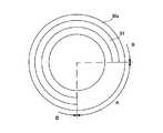
本実施形態に係るエッジリング30は、エッジリング30の周方向の一部にエッジリング30を構成する部材の熱伝導率と異なる部分を備える。以下では、前記部分の一例として、溝51を備えるエッジリング30aについて説明する。図3は、本実施形態に係るエッジリング30aの裏面図である。本実施形態のエッジリング30aは、静電チャック25に載置する側の面に溝51を備える。溝51は、エッジリング30aの裏面においてエッジリング30aを周方向に分ける複数の位相の一部に等間隔でなく配置される。図2の例では、領域Aで示す位相の部分には、溝51は形成されていない。溝51は、周方向の領域Bで示す位相の部分に形成されている。なお、溝51の深さについては、温度分布が均一になるように、適宜調整する。溝51は、エッジリング30aの裏面の高さを変更した空間である。なお、後述する変形例の溝や孔、段差等についても同様に、エッジリングの裏面の高さを変更した空間である。[Edge ring configuration]
The
[溝の位置]
エッジリング30と静電チャック25との間の熱の伝達と溝の位置との関係について図2を参照して説明する。図2では、領域A、Bにおけるエッジリング30aの断面図を示す。[Groove position]
The relationship between the heat transfer between the
エッジリング30aは、領域Aに溝が設けられず、平面である。それに対して、エッジリング30aは、領域Bに周方向に弧状の溝51が一つ設けられている。エッジリング30aには、プラズマPからエッジリング30aの上面30a1に熱H1が入熱する。入熱した熱H1は、エッジリング30aを通って、エッジリング30aの静電チャック25側の裏面30a2から熱H2となって出熱する。これにより、エッジリング30aが抜熱される。エッジリング30aの領域Bの裏面30a2が、静電チャック25の載置面25b1と接触する面積は、エッジリング30aの領域Aの裏面30a2が、静電チャック25の載置面25b1と接触する面積より単位面積当たりで小さくなっている。そのため、エッジリング30aの領域Aと領域Bを比較すると、領域Bの方が、載置面25b1に対する熱伝達性が低くなっている。したがって、領域Bにおいて、裏面30a2から単位面積当たりで抜熱される熱H2は、領域Aの場合より少なくなる。そのため、領域Bでは、プラズマPからの熱H1が領域Aと比較して抜熱され難くなり、上面30a1の温度が領域Aの場合より高い高温化領域RHが生じる。 The
このように、エッジリング30aは、周方向に溝51が設けられていない領域(領域A)と、周方向に溝51が設けられている領域(領域B)と、を有する。領域Aと、領域Bとでは、エッジリング30aの裏面30a2から抜熱される単位面積当たりの熱H2が異なる。そのため、エッジリング30aの上面30a1は、領域Aより領域Bのほうが、温度が高くなる傾向になる。このように、エッジリング30aは、周方向に溝51が設けられている領域と、設けられていない領域とを有することにより、エッジリング30aのプラズマP側の上面30a1に温度分布が発生する。本実施形態の載置台アセンブリ5では、載置面25b1に載置される面を平面とした比較例のエッジリング300において領域Bでは、領域Aに対して相対的に温度が低くなっているとすると、エッジリング30aは領域Bに溝51を設けることにより、エッジリング30aと静電チャック25との間の熱伝達性を悪くして、エッジリング30aの領域Bの温度を上昇させるように制御できる。これにより、エッジリング30a全体の温度を均一にすることができる。 As described above, the
<効果・作用>
以上に説明したように、本実施形態に係る載置台アセンブリ5は、載置台10の載置面に対向する裏面であって、エッジリング30の周方向の一部にエッジリング30を構成する部材(シリコン等)の熱伝導率と異なる部分の一例として溝51を有する。そして、前記部分は、エッジリング30を周方向に分ける複数の位相の一部に等間隔でなく配置される。これにより、プラズマ処理を行う際のエッジリング30aの温度を均一にすることができる。また、これにより、プラズマ処理を行う際のエッジリング30aの温度にあえて相対的に高い領域と低い領域とをつくることができる。<Effect / action>
As described above, the mounting
さらに、例えば、主に基板Wのエッジ領域におけるCD(Critical Dimension)の偏りや、エッチンレートの偏りを補正したい位相、若しくは、補正したい位相以外のエッジリング30の裏面に溝51を設けることで、CD等の偏りを是正することにより、エッジリング300様な溝を有しないものと、同等に扱うことができる。このことから、基板の温度制御に使用されるその他のパーツの使用が不要になったり、また、エッジリング30のセンタリングのような設置作業工数の増加することなく、より安価で、簡易に温度を均一にし、CD等の偏りを補正することができる。 Further, for example, by providing a
<変形例>
[エッジリングの変形例1]
図4は、本実施形態に係るエッジリング30aの変形例の一例であるエッジリング30bの裏面を示す図である。<Modification example>
[Modification example 1 of edge ring]
FIG. 4 is a diagram showing the back surface of the
エッジリング30bの裏面は、エッジリング30bの周方向の一部にエッジリング30bを構成する部材の熱伝導率と異なる部分の一例として溝52を備える。溝52は径方向の幅が場所によって異なる。これによって、周方向の温度分布の調整をより細かく行うことができる。例えば、静電チャック25の載置面25b1に載置される面を平面としたエッジリング300において、領域Aの温度が一番高く、領域B、領域Cの順番で温度の低くなっているとする。その場合に、エッジリング30bは、領域Aには溝を形成されていない。また、エッジリング30bは、領域B、領域Cに溝52が形成されている。それによって、領域Aに対して、領域B、領域Cの方が、エッジリング30bと静電チャック25の間の熱伝達性が低くなっている。さらに、エッジリング30bの溝52について、径方向の幅が、領域Bより領域Cの方が広くなっている。それによって、溝52が形成されている領域B、領域Cにおいても、エッジリング30bと静電チャック25の間の熱伝達性が異なる。すなわち、エッジリング30bの領域Bに対して、領域Cの方が、エッジリング30bと静電チャック25の間の熱伝達性が低くなっている。このようにして、より細かく温度の調整を行うことができる。したがって、エッジリング30bの温度分布の均一性を高めることができる。 The back surface of the
[エッジリングの変形例2]
図5は、本実施形態に係るエッジリング30aの変形例の一例であるエッジリング30cの裏面を示す図である。[Modification example 2 of edge ring]
FIG. 5 is a diagram showing the back surface of the
エッジリング30cは、エッジリング30cの周方向の一部にエッジリング30cを構成する部材の熱伝導率と異なる部分の一例として径方向に複数の溝53(53a、53b、53c)を備える。このように、径方向に複数の溝53、すなわち、径方向にエッジリング30cの周方向の一部にエッジリング30cを構成する部材の熱伝導率と異なる部分を複数備えることにより、径方向の温度分布をより均一にすることができる。さらに、溝53の長さを調整することにより、周方向の温度分布をより均一にすることができる。したがって、エッジリング30cの温度分布の均一性を高めることができる。 The
[エッジリングの変形例3]
図6は、本実施形態に係るエッジリング30aの変形例の一例であるエッジリング30dの裏面を示す図である。[Modification example 3 of edge ring]
FIG. 6 is a diagram showing the back surface of the
エッジリング30dは、溝の代わりにエッジリング30dの周方向の一部にエッジリング30dを構成する部材の熱伝導率と異なる部分の一例として複数の円形の孔54を備える。当該孔54の孔の径や数をエッジリング30dの場所により変更することにより、エッジリング30dと静電チャック25との間の熱伝達性を変更することができる。これにより、エッジリング30dの温度分布の均一性を高めることができる。なお、孔54の上面視した形状については、図6の円に限らず、例えば、三角、四角等の多角形でもよいし、楕円形でもよい。 The
[エッジリングの変形例4]
図7は、本実施形態に係るエッジリング30aの変形例の一例であるエッジリング30eの断面を示す図である。[Modification example 4 of edge ring]
FIG. 7 is a diagram showing a cross section of the
エッジリング30eは、エッジリング30eの周方向の一部にエッジリング30eを構成する部材の熱伝導率と異なる部分の一例として溝55を備える。また、溝55の内部に充填部材55aが埋め込まれている。充填部材55aは、気体、液体、固体のいずれであってもよい。充填部材55aとしては、エッジリング30eを構成する部材の熱伝導性より低い熱伝導性を有する部材を用いる。エッジリング30eの部材の熱伝導率と異なる充填部材55aを用いることによって、エッジリング30eと静電チャック25との間の熱伝達性を変更することができる。これにより、エッジリング30eの温度分布の均一性を高めることができる。 The
[エッジリングの変形例5]
図8は、本実施形態に係るエッジリング30aの変形例の一例であるエッジリング30fの断面を示す図である。[Modification example 5 of edge ring]
FIG. 8 is a diagram showing a cross section of the edge ring 30f, which is an example of a modification of the
エッジリング30fは、エッジリング30fの周方向の一部にエッジリング30fを構成する部材の熱伝導率と異なる部分の一例として径方向に溝の深さの異なる段差56を備える。このような段差のように溝の深さを径方向に変更することにより、径方向の温度分布をより細かく調整することができる。これにより、エッジリング30fの温度分布の均一性を高めることができる。 The edge ring 30f includes a
[エッジリングの変形例6]
図9は、本実施形態に係るエッジリング30aの変形例の一例であるエッジリング30gの断面を示す図である。[Modification example 6 of edge ring]
FIG. 9 is a diagram showing a cross section of an
エッジリング30gは、エッジリング30gの周方向の一部にエッジリング30gを構成する部材の熱伝導率と異なる部分の一例として貫通溝57を備える。エッジリング30aの溝51の部分が貫通溝57となっている。また、貫通溝57に、充填部材57aを備える。充填部材57aは、エッジリング30gの部材の熱伝導率と異なる充填部材57aを用いることによって、エッジリング30gと静電チャック25との間の熱伝達性を変更することができる。これにより、エッジリング30gの温度分布の均一性を高めることができる。 The
[エッジリングの変形例7]
図10は、本実施形態に係るエッジリング30aの変形例の一例であるエッジリング30hの裏面を示す図である。[Modification example 7 of edge ring]
FIG. 10 is a diagram showing the back surface of the
エッジリング30hは、円周方向にエッジリング30haとエッジリング30hbに分割されている。エッジリング30haとエッジリング30hbは、互いに熱伝導率の異なる部材で形成されている。例えば、エッジリング30haは、炭化ケイ素SiCで形成されている。エッジリング30hbは、ケイ素Siで形成されている。これによって、エッジリング30gと静電チャック25との間の熱伝達性を変更することができる。例えば、エッジリング30hbは、エッジリング30hの周方向の一部にエッジリング30hを構成する部材の熱伝導率と異なる部分の一例である。これにより、エッジリング30hの温度分布の均一性を高めることができる。 The
[載置台アセンブリの変形例1]
上記の実施例及び変形例では、載置台の載置面に対向する裏面に、エッジリング30の周方向の一部にエッジリング30を構成する部材の熱伝導率と異なる部分の一例として、エッジリング30に溝等を設けたが、熱伝導率の異なる部分をエッジリング30に備えることに限らない。載置台アセンブリの変形例1として、熱伝導率の異なる部分をシート部材に備える例を示す。[Modification example 1 of mounting table assembly]
In the above-described embodiment and modification, an edge is provided as an example of a portion of the back surface of the mounting table facing the mounting surface, which is different from the thermal conductivity of the member constituting the
図11は、本実施形態に係る載置台アセンブリの変形例の一例の断面を示す図である。図11の変形例では、エッジリング300と静電チャック25の間に、熱を伝達するシート部材61を備える。そして、シート部材61は、エッジリングの温度を下げたい領域には、熱伝導率の高い部材、エッジリングの温度を上げたい領域には、熱伝導率の低い部材で構成する。これによって、エッジリング300と静電チャック25との間の熱伝達性を変更することができる。このように、プラズマ処理時のエッジリング300の温度分布に応じた位置に熱伝導率が異なる部分を有するシート部材を、有するようにしてもよい。これにより、エッジリングの温度分布の均一性を高めることができる。 FIG. 11 is a diagram showing a cross section of an example of a modification of the mounting table assembly according to the present embodiment. In the modified example of FIG. 11, a
なお、シート部材の熱伝導率を低くするために、溝や孔を備えるようにしてもよい。また、周方向の一部、例えば、エッジリングの温度を下げたい領域、にのみシート部材を備えるようにしてもよい。さらに、溝を有するエッジリングと組み合わせてもよい。 In addition, in order to lower the thermal conductivity of the sheet member, grooves and holes may be provided. Further, the seat member may be provided only in a part in the circumferential direction, for example, a region where the temperature of the edge ring is desired to be lowered. Further, it may be combined with an edge ring having a groove.
[載置台アセンブリの変形例2]
次に、載置台アセンブリ5の変形例2として、熱伝導率の異なる部分を静電チャックに備える例を示す。図12は、本実施形態に係る載置台アセンブリの変形例の一例の断面を示す図である。図12の変形例では、エッジリング30aの溝51に対応する部分に、静電チャック25dに溝70を設ける。これによって、エッジリング30と静電チャック25dとの間の熱伝達性を変更することができる。そして、エッジリングの温度分布の均一性を高めることができる。なお、溝を有するエッジリングやシート部材の少なくとも1つと組み合わせてもよい。[Modification example 2 of mounting table assembly]
Next, as a modification 2 of the mounting
今回開示された本実施形態に係る載置台、基板処理装置及びエッジリングは、すべての点において例示であって制限的なものではないと考えられるべきである。上記の実施形態は、添付の請求の範囲及びその主旨を逸脱することなく、様々な形態で変形及び改良が可能である。上記複数の実施形態に記載された事項は、矛盾しない範囲で他の構成も取り得ることができ、また、矛盾しない範囲で組み合わせることができる。 It should be considered that the mounting table, the substrate processing device, and the edge ring according to the present embodiment disclosed this time are exemplary in all respects and are not restrictive. The above-described embodiment can be modified and improved in various forms without departing from the scope of the appended claims and the gist thereof. The matters described in the plurality of embodiments may have other configurations within a consistent range, and may be combined within a consistent range.
本開示の基板処理装置は、Capacitively Coupled Plasma(CCP)、Inductively Coupled Plasma(ICP)、Radial Line Slot Antenna(RLSA)、Electron Cyclotron Resonance Plasma(ECR)、Helicon Wave Plasma(HWP)のどのタイプでも適用可能である。 The substrate processing apparatus of the present disclosure includes Capacitively Coupled Plasma (CCP), Inductively Coupled Plasma (ICP), Radial Line Slot Antenna (RLSA), Electron Cyclotron Res Is.
1 基板処理装置
5 載置台アセンブリ
10 載置台
11 基台
25 静電チャック
30 エッジリング
30a〜30h エッジリング
51 溝
52 溝
53 溝
54 孔
55 溝
55a 充填部材
56 段差
57 貫通溝
57a 充填部材
61 シート部材
70 溝
W 基板1
Claims (10)
Translated fromJapanese前記エッジリングは、前記載置台の載置面に対向する裏面であって、前記エッジリングの周方向の一部に前記エッジリングを構成する部材の熱伝導率と異なる部分を有する、
載置台アセンブリ。A mounting table assembly comprising a mounting table on which a substrate to be subjected to plasma treatment is mounted, and an edge ring mounted on the above-described table around the substrate.
The edge ring is a back surface facing the mounting surface of the above-mentioned stand, and has a portion different from the thermal conductivity of the members constituting the edge ring in a part in the circumferential direction of the edge ring.
Mounting platform assembly.
請求項1に記載の載置台アセンブリ。The portions are not evenly spaced in parts of a plurality of phases that divide the edge ring in the circumferential direction.
The mounting table assembly according to claim 1.
請求項1又は2に記載の載置台アセンブリ。The portion is a space in which the height of the back surface of the edge ring is changed.
The mounting table assembly according to claim 1 or 2.
請求項3に記載の載置台アセンブリ。The portion is a groove or a step provided on the back surface of the edge ring.
The mounting table assembly according to claim 3.
請求項1から請求項4のいずれか1項に記載の載置台アセンブリ。A member having a thermal conductivity lower than that of the edge ring is embedded in the portion.
The mounting table assembly according to any one of claims 1 to 4.
請求項1から請求項5のいずれか1項に記載の載置台アセンブリ。A plurality of said portions are provided in the radial direction of the edge ring.
The mounting table assembly according to any one of claims 1 to 5.
請求項1から請求項6のいずれか1項に記載の載置台アセンブリ。The portion is arranged according to the temperature distribution of the edge ring during plasma processing.
The mounting table assembly according to any one of claims 1 to 6.
請求項1から請求項7のいずれか1項に記載の載置台アセンブリ。The sheet member is provided between the edge ring and the above-mentioned mounting surface at a position corresponding to the temperature distribution of the edge ring during plasma treatment.
The mounting table assembly according to any one of claims 1 to 7.
基板処理装置。A substrate processing apparatus comprising the mounting table assembly according to any one of claims 1 to 8.
前記載置台の載置面に対向する裏面であって、前記エッジリングの周方向の一部に前記エッジリングを構成する部材の熱伝導率と異なる部分を有する、エッジリング。An edge ring that is placed on a mounting table on which the board is placed around the substrate to be plasma-treated.
An edge ring which is a back surface facing the mounting surface of the above-mentioned stand and has a portion different from the thermal conductivity of the members constituting the edge ring in a part in the circumferential direction of the edge ring.
Priority Applications (2)
| Application Number | Priority Date | Filing Date | Title |
|---|---|---|---|
| JP2019134077AJP2021019099A (en) | 2019-07-19 | 2019-07-19 | Placement table assembly, substrate processing device, and edge ring |
| US16/925,806US20210020408A1 (en) | 2019-07-19 | 2020-07-10 | Substrate support assembly, substrate processing apparatus, and edge ring |
Applications Claiming Priority (1)
| Application Number | Priority Date | Filing Date | Title |
|---|---|---|---|
| JP2019134077AJP2021019099A (en) | 2019-07-19 | 2019-07-19 | Placement table assembly, substrate processing device, and edge ring |
Publications (1)
| Publication Number | Publication Date |
|---|---|
| JP2021019099Atrue JP2021019099A (en) | 2021-02-15 |
Family
ID=74343946
Family Applications (1)
| Application Number | Title | Priority Date | Filing Date |
|---|---|---|---|
| JP2019134077APendingJP2021019099A (en) | 2019-07-19 | 2019-07-19 | Placement table assembly, substrate processing device, and edge ring |
Country Status (2)
| Country | Link |
|---|---|
| US (1) | US20210020408A1 (en) |
| JP (1) | JP2021019099A (en) |
Cited By (1)
| Publication number | Priority date | Publication date | Assignee | Title |
|---|---|---|---|---|
| JP2022171027A (en)* | 2021-04-30 | 2022-11-11 | 東京エレクトロン株式会社 | Substrate support and processing device |
Families Citing this family (2)
| Publication number | Priority date | Publication date | Assignee | Title |
|---|---|---|---|---|
| US12165851B2 (en)* | 2021-07-29 | 2024-12-10 | Taiwan Semiconductor Manufacturing Company, Ltd. | Plasma processing method for manufacturing semiconductor structure |
| JP7629099B2 (en)* | 2022-06-07 | 2025-02-12 | 株式会社日立ハイテク | Plasma Processing Equipment |
Family Cites Families (3)
| Publication number | Priority date | Publication date | Assignee | Title |
|---|---|---|---|---|
| US20040261946A1 (en)* | 2003-04-24 | 2004-12-30 | Tokyo Electron Limited | Plasma processing apparatus, focus ring, and susceptor |
| JP2008251742A (en)* | 2007-03-29 | 2008-10-16 | Tokyo Electron Ltd | Substrate treating apparatus, and substrate mounting base on which focus ring is mounted |
| KR101559913B1 (en)* | 2009-06-25 | 2015-10-27 | 삼성전자주식회사 | Plasma dry etching apparatus |
- 2019
- 2019-07-19JPJP2019134077Apatent/JP2021019099A/enactivePending
- 2020
- 2020-07-10USUS16/925,806patent/US20210020408A1/ennot_activeAbandoned
Cited By (1)
| Publication number | Priority date | Publication date | Assignee | Title |
|---|---|---|---|---|
| JP2022171027A (en)* | 2021-04-30 | 2022-11-11 | 東京エレクトロン株式会社 | Substrate support and processing device |
Also Published As
| Publication number | Publication date |
|---|---|
| US20210020408A1 (en) | 2021-01-21 |
Similar Documents
| Publication | Publication Date | Title |
|---|---|---|
| JP7175114B2 (en) | Mounting table and electrode member | |
| KR102432446B1 (en) | Mounting table and plasma processing apparatus | |
| JP6974088B2 (en) | Plasma processing equipment and plasma processing method | |
| JP7213927B2 (en) | Substrate processing system | |
| JP6861579B2 (en) | Plasma processing equipment, electrostatic adsorption method and electrostatic adsorption program | |
| WO2019239944A1 (en) | Plasma processing device, and method for controlling high-frequency power supply of plasma processing device | |
| JP6573498B2 (en) | Plasma processing equipment | |
| JP2018107433A (en) | Focus ring and substrate processing apparatus | |
| CN111095498B (en) | Mounting table, substrate processing apparatus, and edge ring | |
| US20180182635A1 (en) | Focus ring and substrate processing apparatus | |
| CN108335963A (en) | Plasma processing apparatus | |
| JP7055040B2 (en) | Placement device and processing device for the object to be processed | |
| KR20170072809A (en) | Plasma processing method and plasma processing apparatus | |
| JP6219227B2 (en) | Heater feeding mechanism and stage temperature control method | |
| JP7390880B2 (en) | Edge ring and substrate processing equipment | |
| JP7531641B2 (en) | Mounting table and substrate processing apparatus | |
| WO2019244700A1 (en) | Plasma processing device and plasma etching method | |
| JP2021019099A (en) | Placement table assembly, substrate processing device, and edge ring | |
| JP2017212051A (en) | Plasma processing method | |
| TW202032715A (en) | Placing table and substrate processing apparatus | |
| JP7278896B2 (en) | Plasma processing method and plasma processing apparatus | |
| JP2019201086A (en) | Processing device, component, and temperature control method | |
| KR102628181B1 (en) | Part for semiconductor manufacturing apparatus and semiconductor manufacturing apparatus | |
| JP7199246B2 (en) | Substrate processing equipment | |
| JP7246451B2 (en) | Plasma processing apparatus and plasma processing method |