JP2021015153A - Display device - Google Patents
Display deviceDownload PDFInfo
- Publication number
- JP2021015153A JP2021015153AJP2019128616AJP2019128616AJP2021015153AJP 2021015153 AJP2021015153 AJP 2021015153AJP 2019128616 AJP2019128616 AJP 2019128616AJP 2019128616 AJP2019128616 AJP 2019128616AJP 2021015153 AJP2021015153 AJP 2021015153A
- Authority
- JP
- Japan
- Prior art keywords
- light source
- period
- light
- line
- image
- Prior art date
- Legal status (The legal status is an assumption and is not a legal conclusion. Google has not performed a legal analysis and makes no representation as to the accuracy of the status listed.)
- Granted
Links
Images


Classifications
- G—PHYSICS
- G02—OPTICS
- G02F—OPTICAL DEVICES OR ARRANGEMENTS FOR THE CONTROL OF LIGHT BY MODIFICATION OF THE OPTICAL PROPERTIES OF THE MEDIA OF THE ELEMENTS INVOLVED THEREIN; NON-LINEAR OPTICS; FREQUENCY-CHANGING OF LIGHT; OPTICAL LOGIC ELEMENTS; OPTICAL ANALOGUE/DIGITAL CONVERTERS
- G02F1/00—Devices or arrangements for the control of the intensity, colour, phase, polarisation or direction of light arriving from an independent light source, e.g. switching, gating or modulating; Non-linear optics
- G02F1/01—Devices or arrangements for the control of the intensity, colour, phase, polarisation or direction of light arriving from an independent light source, e.g. switching, gating or modulating; Non-linear optics for the control of the intensity, phase, polarisation or colour
- G02F1/13—Devices or arrangements for the control of the intensity, colour, phase, polarisation or direction of light arriving from an independent light source, e.g. switching, gating or modulating; Non-linear optics for the control of the intensity, phase, polarisation or colour based on liquid crystals, e.g. single liquid crystal display cells
- G02F1/133—Constructional arrangements; Operation of liquid crystal cells; Circuit arrangements
- G02F1/1333—Constructional arrangements; Manufacturing methods
- G02F1/1334—Constructional arrangements; Manufacturing methods based on polymer dispersed liquid crystals, e.g. microencapsulated liquid crystals
- G—PHYSICS
- G09—EDUCATION; CRYPTOGRAPHY; DISPLAY; ADVERTISING; SEALS
- G09G—ARRANGEMENTS OR CIRCUITS FOR CONTROL OF INDICATING DEVICES USING STATIC MEANS TO PRESENT VARIABLE INFORMATION
- G09G3/00—Control arrangements or circuits, of interest only in connection with visual indicators other than cathode-ray tubes
- G09G3/20—Control arrangements or circuits, of interest only in connection with visual indicators other than cathode-ray tubes for presentation of an assembly of a number of characters, e.g. a page, by composing the assembly by combination of individual elements arranged in a matrix no fixed position being assigned to or needed to be assigned to the individual characters or partial characters
- G09G3/34—Control arrangements or circuits, of interest only in connection with visual indicators other than cathode-ray tubes for presentation of an assembly of a number of characters, e.g. a page, by composing the assembly by combination of individual elements arranged in a matrix no fixed position being assigned to or needed to be assigned to the individual characters or partial characters by control of light from an independent source
- G09G3/3406—Control of illumination source
- G09G3/3413—Details of control of colour illumination sources
- G—PHYSICS
- G09—EDUCATION; CRYPTOGRAPHY; DISPLAY; ADVERTISING; SEALS
- G09G—ARRANGEMENTS OR CIRCUITS FOR CONTROL OF INDICATING DEVICES USING STATIC MEANS TO PRESENT VARIABLE INFORMATION
- G09G3/00—Control arrangements or circuits, of interest only in connection with visual indicators other than cathode-ray tubes
- G09G3/20—Control arrangements or circuits, of interest only in connection with visual indicators other than cathode-ray tubes for presentation of an assembly of a number of characters, e.g. a page, by composing the assembly by combination of individual elements arranged in a matrix no fixed position being assigned to or needed to be assigned to the individual characters or partial characters
- G09G3/34—Control arrangements or circuits, of interest only in connection with visual indicators other than cathode-ray tubes for presentation of an assembly of a number of characters, e.g. a page, by composing the assembly by combination of individual elements arranged in a matrix no fixed position being assigned to or needed to be assigned to the individual characters or partial characters by control of light from an independent source
- G09G3/36—Control arrangements or circuits, of interest only in connection with visual indicators other than cathode-ray tubes for presentation of an assembly of a number of characters, e.g. a page, by composing the assembly by combination of individual elements arranged in a matrix no fixed position being assigned to or needed to be assigned to the individual characters or partial characters by control of light from an independent source using liquid crystals
- G—PHYSICS
- G02—OPTICS
- G02F—OPTICAL DEVICES OR ARRANGEMENTS FOR THE CONTROL OF LIGHT BY MODIFICATION OF THE OPTICAL PROPERTIES OF THE MEDIA OF THE ELEMENTS INVOLVED THEREIN; NON-LINEAR OPTICS; FREQUENCY-CHANGING OF LIGHT; OPTICAL LOGIC ELEMENTS; OPTICAL ANALOGUE/DIGITAL CONVERTERS
- G02F1/00—Devices or arrangements for the control of the intensity, colour, phase, polarisation or direction of light arriving from an independent light source, e.g. switching, gating or modulating; Non-linear optics
- G02F1/01—Devices or arrangements for the control of the intensity, colour, phase, polarisation or direction of light arriving from an independent light source, e.g. switching, gating or modulating; Non-linear optics for the control of the intensity, phase, polarisation or colour
- G02F1/13—Devices or arrangements for the control of the intensity, colour, phase, polarisation or direction of light arriving from an independent light source, e.g. switching, gating or modulating; Non-linear optics for the control of the intensity, phase, polarisation or colour based on liquid crystals, e.g. single liquid crystal display cells
- G02F1/133—Constructional arrangements; Operation of liquid crystal cells; Circuit arrangements
- G02F1/1333—Constructional arrangements; Manufacturing methods
- G02F1/1335—Structural association of cells with optical devices, e.g. polarisers or reflectors
- G02F1/1336—Illuminating devices
- G02F1/133615—Edge-illuminating devices, i.e. illuminating from the side
- G—PHYSICS
- G09—EDUCATION; CRYPTOGRAPHY; DISPLAY; ADVERTISING; SEALS
- G09G—ARRANGEMENTS OR CIRCUITS FOR CONTROL OF INDICATING DEVICES USING STATIC MEANS TO PRESENT VARIABLE INFORMATION
- G09G2310/00—Command of the display device
- G09G2310/02—Addressing, scanning or driving the display screen or processing steps related thereto
- G09G2310/0235—Field-sequential colour display
- G—PHYSICS
- G09—EDUCATION; CRYPTOGRAPHY; DISPLAY; ADVERTISING; SEALS
- G09G—ARRANGEMENTS OR CIRCUITS FOR CONTROL OF INDICATING DEVICES USING STATIC MEANS TO PRESENT VARIABLE INFORMATION
- G09G2310/00—Command of the display device
- G09G2310/08—Details of timing specific for flat panels, other than clock recovery
- G—PHYSICS
- G09—EDUCATION; CRYPTOGRAPHY; DISPLAY; ADVERTISING; SEALS
- G09G—ARRANGEMENTS OR CIRCUITS FOR CONTROL OF INDICATING DEVICES USING STATIC MEANS TO PRESENT VARIABLE INFORMATION
- G09G2320/00—Control of display operating conditions
- G09G2320/02—Improving the quality of display appearance
- G09G2320/0233—Improving the luminance or brightness uniformity across the screen
- G—PHYSICS
- G09—EDUCATION; CRYPTOGRAPHY; DISPLAY; ADVERTISING; SEALS
- G09G—ARRANGEMENTS OR CIRCUITS FOR CONTROL OF INDICATING DEVICES USING STATIC MEANS TO PRESENT VARIABLE INFORMATION
- G09G2320/00—Control of display operating conditions
- G09G2320/06—Adjustment of display parameters
- G09G2320/0626—Adjustment of display parameters for control of overall brightness
Landscapes
- Physics & Mathematics (AREA)
- Engineering & Computer Science (AREA)
- Chemical & Material Sciences (AREA)
- General Physics & Mathematics (AREA)
- Crystallography & Structural Chemistry (AREA)
- Theoretical Computer Science (AREA)
- Computer Hardware Design (AREA)
- Nonlinear Science (AREA)
- Dispersion Chemistry (AREA)
- Mathematical Physics (AREA)
- Optics & Photonics (AREA)
- Control Of Indicators Other Than Cathode Ray Tubes (AREA)
- Liquid Crystal (AREA)
- Liquid Crystal Display Device Control (AREA)
Abstract
Translated fromJapaneseDescription
Translated fromJapanese本発明は、表示装置に関する。 The present invention relates to a display device.
液晶を利用した表示装置において、表示パネルの側面側に光源を設ける構成が知られている(例えば、特許文献1)。 In a display device using a liquid crystal, a configuration in which a light source is provided on the side surface side of the display panel is known (for example, Patent Document 1).
特許文献1のような表示装置では、表示パネルのうち光源により近い側が相対的に明るくなり、光源からより遠い側が相対的に暗くなる。このため、表示パネルと光源との位置関係によって画像の輝度分布に偏りが生じるという問題があった。 In a display device such as
本発明は、上記の課題に鑑みてなされたもので、表示パネルと光源との位置関係による画像の輝度分布の偏りを低減可能な表示装置を提供することを目的とする。 The present invention has been made in view of the above problems, and an object of the present invention is to provide a display device capable of reducing the bias of the brightness distribution of an image due to the positional relationship between the display panel and the light source.
本発明の一態様による表示装置は、対向する2枚の基板の間に液晶が封入され、複数のライン画像を走査方向に並べてフレーム画像を表示させる表示パネルと、前記表示パネルの一側面側から光を照射する光源とを備え、1つの前記フレーム画像に対して割り当てられる1フレーム期間は、画像表示期間と輝度補正期間を含み、前記輝度補正期間における前記表示パネルの輝度は、前記一側面の反対側に近いほど高い。 In the display device according to one aspect of the present invention, a display panel in which a liquid crystal is enclosed between two opposing substrates to display a frame image by arranging a plurality of line images in the scanning direction, and from one side surface side of the display panel. A light source for irradiating light is provided, and one frame period assigned to one frame image includes an image display period and a brightness correction period, and the brightness of the display panel in the brightness correction period is the brightness of the one side surface. The closer it is to the other side, the higher it is.
以下に、本発明の各実施の形態について、図面を参照しつつ説明する。なお、開示はあくまで一例にすぎず、当業者において、発明の主旨を保っての適宜変更について容易に想到し得るものについては、当然に本発明の範囲に含有されるものである。また、図面は説明をより明確にするため、実際の態様に比べ、各部の幅、厚さ、形状等について模式的に表される場合があるが、あくまで一例であって、本発明の解釈を限定するものではない。また、本明細書と各図において、既出の図に関して前述したものと同様の要素には、同一の符号を付して、詳細な説明を適宜省略することがある。 Hereinafter, embodiments of the present invention will be described with reference to the drawings. It should be noted that the disclosure is merely an example, and those skilled in the art can easily conceive of appropriate changes while maintaining the gist of the invention are naturally included in the scope of the present invention. Further, in order to clarify the explanation, the drawings may schematically represent the width, thickness, shape, etc. of each part as compared with the actual embodiment, but this is just an example, and the interpretation of the present invention is used. It is not limited. Further, in the present specification and each figure, the same elements as those described above with respect to the above-mentioned figures may be designated by the same reference numerals, and detailed description thereof may be omitted as appropriate.
(実施形態1)
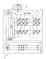
図1は、表示装置100の主要構成を示す模式的な回路図である。表示装置100は、液晶表示パネルPと、光源装置Lとを備える。液晶表示パネルPは、表示部7と、信号出力回路8と、走査回路9と、VCOM駆動回路10と、タイミングコントローラ13と、電源回路14とを備える。以下、表示部7が面する液晶表示パネルPの一面を表示面とし、他面を背面とする。また、表示装置100の側方と記載した場合、表示装置100を基準として表示面と背面との対向方向に交差(例えば、直交)する方向に位置する。(Embodiment 1)
FIG. 1 is a schematic circuit diagram showing a main configuration of the
表示部7には、複数の画素Pixがマトリクス状に配置されている。画素Pixは、スイッチング素子1と、2つの電極とを含む。図1及び後述する図2では、2つの電極として、画素電極2と、共通電極6とを図示している。 A plurality of pixel Pix are arranged in a matrix on the
図2は、液晶表示パネルPの概略断面図である。液晶表示パネルPは、対向する2枚の基板と、当該2枚の基板の間に封入された液晶3を有する。以下、当該2枚の基板の一方を第1基板30とし、他方を第2基板20とする。 FIG. 2 is a schematic cross-sectional view of the liquid crystal display panel P. The liquid crystal display panel P has two opposing substrates and a
第1基板30は、透光性のガラス基板35と、ガラス基板35の第2基板20側に積層された画素電極2と、画素電極2を覆うように第2基板20側に積層された絶縁層55とを含む。画素電極2は、画素Pix毎に個別に設けられる。第2基板20は、透光性のガラス基板21と、ガラス基板21の第1基板30側に積層された共通電極6と、共通電極6を覆うように第1基板30側に積層された絶縁層56とを含む。共通電極6は、複数の画素Pixで共有される板状又は膜状の形状を有する。 The
実施形態1の液晶3は、高分子分散型液晶である。具体的には、液晶3は、バルク51と、微粒子52とを含む。微粒子52は、バルク51内で画素電極2と共通電極6との電位差に応じて配向が変化する。画素Pix毎に画素電極2の電位が個別に制御されることで、画素Pix毎に少なくとも透光及び分散のいずれかの度合いが制御される。 The
図2を参照して説明した実施形態1では、画素電極2と共通電極6は、液晶3を挟むように対向するが、液晶表示パネルPは、1つの基板に画素電極2と共通電極6が設けられて画素電極2と共通電極6によって発生する電界によって液晶3の配向が制御される構成であってもよい。 In the first embodiment described with reference to FIG. 2, the
次に、画素電極2及び共通電極6の電位を制御する仕組みについて説明する。図1に示すようにスイッチング素子1は、例えば薄膜トランジスタ(TFT:Thin Film Transistor)等、半導体を用いたスイッチング素子である。スイッチング素子1のソース又はドレインの一方は、2つの電極の一方(画素電極2)と接続される。スイッチング素子1のソース又はドレインの他方が信号線4と接続される。スイッチング素子1のゲートは、走査線5と接続される。走査線5は、走査回路9の制御下で、スイッチング素子1のソース−ドレイン間を開閉するための電位を与える。当該電位の制御は、走査回路9が行う。 Next, a mechanism for controlling the potentials of the
図1に示す例では、複数の信号線4は、画素Pixの並び方向のうち一方(行方向)に沿って並ぶ。信号線4は、画素Pixの並び方向のうち他方(列方向)に沿って延出する。信号線4は、列方向に並ぶ複数の画素Pixのスイッチング素子1で共有される。複数の走査線5は、列方向に沿って並ぶ。走査線5は、行方向に沿って延出する。走査線5は、行方向に並ぶ複数の画素Pixのスイッチング素子1で共有される。 In the example shown in FIG. 1, the plurality of
実施形態の説明では、走査線5の延出方向をX方向とし、複数の走査線5が並ぶ方向をY方向とする。また、図1では、複数の走査線5のうちY方向の両端に配置されたものの一方を走査線5aとし、他方を走査線5bとしている。 In the description of the embodiment, the extending direction of the scanning lines 5 is the X direction, and the direction in which the plurality of scanning lines 5 are lined up is the Y direction. Further, in FIG. 1, one of a plurality of scanning lines 5 arranged at both ends in the Y direction is designated as a
共通電極6は、VCOM駆動回路10と接続される。VCOM駆動回路10は、共通電極6に共通電位として機能する電位を与える。走査回路9が走査線5に対して駆動信号として機能する電位を与えるタイミングで、信号出力回路8が信号線4に対して後述する階調信号を出力することで、画素電極2と共通電極6との間に形成された蓄積容量と容量性負荷である液晶(微粒子52)を充電する。これによって、画素Pixと共通電極6との間の電圧は階調信号に対応した電圧となる。駆動信号が与えられなくなった後、蓄積容量と容量性負荷である液晶(微粒子52)は階調信号を保持する。液晶(微粒子52)の散乱度は、各画素Pixの電圧と共通電極6の電圧に応じて制御される。例えば、液晶3は各画素Pixの電圧と共通電極6との間の電圧が大きくなるほど散乱度が大きくなるような高分子分散型液晶を用いてもよいし、各画素Pixの電圧と共通電極6との間の電圧が小さくなるほど散乱度が大きくなるような高分子分散型液晶を用いてもよい。 The
図2に示すように、液晶表示パネルPの側方には、光源装置Lが配置されている。光源装置Lは、光源11と、光源駆動回路12とを備える。光源11は、赤色の光を発する第1光源11Rと、緑色の光を発する第2光源11Gと、青色の光を発する第3光源11Bと、を有する。第1光源11R、第2光源11G、第3光源11Bはそれぞれ、光源駆動回路12の制御下で発光する。実施形態1の第1光源11R、第2光源11G及び第3光源11Bは、例えば発光ダイオード(LED:Light Emitting Diode)のような発光素子を用いた光源であるが、これに限られるものでなく、発光タイミングを制御可能な光源であればよい。光源駆動回路12は、タイミングコントローラ13の制御下で第1光源11R、第2光源11G、第3光源11Bの発光タイミングを制御する。 As shown in FIG. 2, a light source device L is arranged on the side of the liquid crystal display panel P. The light source device L includes a
光源11から光が照射されると、表示部7は、Y方向の一側面側から照射される光によって照明される。各画素Pixは、Y方向の一側面側から照射される光を透過または散乱させる。散乱の度合いは、階調信号に応じて制御された液晶3の状態による。 When light is emitted from the
タイミングコントローラ13は、信号出力回路8、走査回路9、VCOM駆動回路10及び光源駆動回路12の動作タイミングを制御する回路である。実施形態では、タイミングコントローラ13は、入力回路15を介して入力された信号に基づいて動作する。 The timing controller 13 is a circuit that controls the operation timing of the signal output circuit 8, the
入力回路15は、表示装置100の外部からの入力信号I(図1参照)に基づいた信号をタイミングコントローラ13及び信号出力回路8に出力する。ある1つの画素Pixに割り当てられるRGBの階調値を示す信号を画素信号とすると、フレーム画像を出力するために入力回路15に入力される入力信号Iは、表示部7に設けられた複数の画素Pixに対する複数の画素信号の集合である。なお、入力回路15は、液晶表示パネルPを構成する基板の1つに設けられてもよいし、液晶表示パネルPから延出する配線等が設けられるフレキシブルプリント基板に実装されてもよいし、液晶表示パネルPの外部に設けられる構成であってもよい。 The
入力回路15からタイミングコントローラ13に入力される信号は、入力信号Iであってもよいし、入力回路15から信号出力回路8に入力信号I又は入力信号Iに基づいて生成された階調信号の入力タイミングを示す信号であってもよい。入力回路15からタイミングコントローラ13に対する入力によって、階調信号を各画素Pixに与えるための駆動信号の出力タイミング及び信号出力回路8の動作タイミングの制御を行うために必要な情報が得られればよい。 The signal input from the
図3は、表示部7と光源11との位置関係及び表示部7の光源11側からその反対側にかけての光の輝度と輝度補正との関係を示す説明図である。図3の「表示部と光源との位置関係」欄で示すように、光源11は、表示部7の一側面側から光を照射する。具体的には、光源11は、表示部7に対してY方向の一端側に配置される。 FIG. 3 is an explanatory diagram showing the positional relationship between the
表示部7に照射された光は液晶3の層(液晶層)の中で減衰するため、光源11から照射された光の輝度は、Y方向の位置によって異なる。具体的には、例えば図3の「表示部の光の輝度と輝度補正との関係」欄に示すグラフGにおける曲線Dのように、光源11に近いほど高輝度であり、光源11から遠ざかるに従って低輝度になる。光源11側からその反対側に向かって生じる輝度の低減の度合いは、光源11により近い側ほど顕著に生じる。 Since the light emitted to the
一方、表示部7における各画素Pixに対して照射される光の輝度は、例えば直線Fで示すように、光源11に対する相対的な位置の遠近に関わらないことが望ましい。そこで、実施形態では、後述する輝度補正期間FI4による輝度補正を適用する。具体的には、実施形態では、例えば曲線Eで示すように、光源11から遠ざかるほど画素Pixで散乱される光の輝度がより高くなるように補正するための制御を適用する。係る輝度補正によって、表示部7に対して照射される光の輝度が表示部7と光源11との位置関係によって曲線Dのようであっても、所定期間中における各画素Pixの光の輝度差をより小さくすることができる。 On the other hand, it is desirable that the brightness of the light emitted to each pixel Pix on the
より具体的には、実施形態では、フレーム画像を表示するフレーム期間FL中に、フレーム画像の画像表示期間とは別の輝度補正期間を設けることで輝度補正を行う。 More specifically, in the embodiment, the brightness correction is performed by providing a brightness correction period different from the image display period of the frame image during the frame period FL for displaying the frame image.
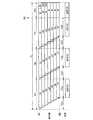
図4は、輝度補正期間を含むフィールドシーケンシャル制御の一例を示すタイムチャートである。図4で例示するように、実施形態1では、1フレーム期間FLに含まれる画像表示期間中にそれぞれ異なる色の光源(例えば、第1光源11R、第2光源11G、第3光源11B)からの光を利用するフィールド期間FI1,FI2,FI3を設ける時分割のカラー表示出力方式(FSC:Field Sequential Color)が採用されている。 FIG. 4 is a time chart showing an example of field sequential control including a luminance correction period. As illustrated in FIG. 4, in the first embodiment, light sources of different colors (for example, the first
具体的には、実施形態1では、1フレーム期間FLに含まれる複数のフィールド期間FI1,FI2,FI3の各々で、それぞれ異なる色の階調値に対応する階調信号が書き込まれる。例えば、画素信号をRGBの階調値で表した場合に(R,G,B)=(r1,g1,b1)であるとする。r1は、RGBの階調値を示す情報を含む入力信号における赤色(R)の階調値であり、表示部7で表示される画像の赤色(R)成分として機能する。g1は、RGBの階調値を示す情報を含む入力信号における緑色(G)の階調値であり、表示部7で表示される画像の緑色(G)成分として機能する。b1は、RGBの階調値を示す情報を含む入力信号における青色(B)の階調値であり、表示部7で表示される画像の青色(B)成分として機能する。この場合、フィールド期間FI1の書込期間FI11に「r1」の階調値に対応する階調信号が書き込まれる。また、フィールド期間FI2の書込期間FI21に「g1」の階調値に対応する階調信号が書き込まれる。また、フィールド期間FI3の書込期間FI31に「b1」の階調値に対応する階調信号が書き込まれる。各フィールド期間に含まれる保持期間FI12,FI22,FI32では、このようにして書込期間に書き込まれたそれぞれ異なる色の階調値に対応する階調信号が保持される。このような各フィールド期間FI1,FI2,FI3における階調信号の書き込み及び保持が、複数の画素Pixの各々で個別に行われる。 Specifically, in the first embodiment, gradation signals corresponding to gradation values of different colors are written in each of the plurality of field periods FI1, FI2, and FI3 included in one frame period FL. For example, it is assumed that (R, G, B) = (r1, g1, b1) when the pixel signal is represented by RGB gradation values. r1 is a red (R) gradation value in the input signal including information indicating the RGB gradation value, and functions as a red (R) component of the image displayed by the
光源11が有する複数の色の光源(例えば、第1光源11R、第2光源11G及び第3光源11B)は、対応するフィールド期間の保持期間内に点灯するよう制御される。実施形態1では、第1光源11Rは赤色の光源、第2光源11Gは緑色の光源、第3光源11Bは青色の光源である。図4等では、保持期間FI12における第1光源11Rの点灯期間を「点灯(R)」で示している。また、図4等では、保持期間FI22における第2光源11Gの点灯期間を「点灯(G)」で示している。また、図4等では、保持期間FI32における第3光源11Bの点灯期間を「点灯(B)」で示している。このように、保持期間に光源11が点灯することで画像が表示される。従って、フィールド期間FI1,FI2,FI3を含む期間は、画像表示期間として機能する。 The light sources of a plurality of colors included in the light source 11 (for example, the first
書込期間FI11,FI21,FI31には、走査回路9による走査線5への駆動信号の出力によって画素Pixに設けられたTFTをオンさせるとともに信号出力回路8による信号線4への階調信号の出力によって画素Pixに階調信号を書き込む信号制御が行われる。従って、共通の走査線5に接続されて当該走査線5に対する駆動信号に応じて同時にオンされる画素行に含まれる複数のPixに対する階調信号の書き込みタイミングは同時になる。このように共通の走査線5に接続される画素行に書き込まれる画像をライン画像とすると、フレーム画像は、走査線5の並び方向に沿って並ぶ複数のライン画像により構成される。ライン画像は、走査線5の延出方向(信号線4の並び方向)に沿って並ぶ複数の画素Pixによって表示出力される画像である。以下、単に「ライン」と記載した場合、特筆しない限り、ライン画像を出力する画素行をさす。 During the writing periods FI11, FI21, and FI31, the TFT provided in the pixel Pix is turned on by the output of the drive signal to the scanning line 5 by the
なお、図4以降のタイムチャートでは、図3の「表示部と光源との位置関係」欄に示すように、表示部7のうち光源11に近い一側面側に(近)の符号を付し、その反対側に(遠)の符号を付すことで、表示部7と光源11との位置関係を示す。 In the time charts after FIG. 4, as shown in the “Positional relationship between the display unit and the light source” column of FIG. 3, one side surface side of the
図4等では、例示的に7ライン分の表示領域に対して出力されるライン画像に係る階調信号制御を図示している。例えば、後述する図6を除く図4、図5、図7、図8では、各書込期間FI11,FI21,FI31中に光源11から遠い側(図1の走査線5b側)から近い側(図1の走査線5a側)に向かって走査線5が順次走査されるよう走査回路9から走査線5へ駆動信号が出力される。これによって、図4に示す7ライン分の表示領域に対して、書込期間FI11中に赤色(R)成分のライン画像R1,R2,R3,R4,R5,R6,R7が順次書き込まれる。また、書込期間FI21中に緑色(G)成分のライン画像G1,G2,G3,G4,G5,G6,G7が順次書き込まれる。また、書込期間FI31中に青色(B)成分のライン画像B1,B2,B3,B4,B5,B6,B7が順次書き込まれる。なお、符号の末尾の番号が異なるライン画像は、異なる走査線5に接続された画素Pixにより出力されるライン画像である。例えば、ライン画像R1とライン画像R2は、異なる走査線5に接続された画素Pixにより出力されるライン画像である。また、号の末尾の番号が同じライン画像は、同じ走査線5に接続された画素Pixにより出力されるライン画像である。例えば、ライン画像R1とライン画像G1とライン画像B1は、同じ走査線5に接続された画素Pixによりそれぞれ異なる期間に出力されるライン画像である。 In FIG. 4 and the like, the gradation signal control related to the line image output to the display area for 7 lines is illustrated. For example, in FIGS. 4, 5, 7, and 8 excluding FIG. 6, which will be described later, in each of the writing periods FI11, FI21, and FI31, the side closer to the light source 11 (scanning
図4等における7ラインの構成及び制御はあくまで説明を分かりやすくするための例示であって、表示部7のライン数を7ラインに制限するものでない。表示部7のライン数は複数であればよく、6以下であってもよいし8以上であってもよい。 The configuration and control of the 7 lines in FIG. 4 and the like are merely examples for making the explanation easy to understand, and the number of lines of the
フレーム期間FLは、画像表示期間(フィールド期間FI1,FI2,FI3)と、輝度補正期間FI4とを含む。具体的には、1フレーム期間FL中には、フィールド期間FI3の後にリセットタイミングBSが設けられ、リセットタイミングBSの後に輝度補正期間FI4が設けられる。 The frame period FL includes an image display period (field period FI1, FI2, FI3) and a brightness correction period FI4. Specifically, during the one-frame period FL, the reset timing BS is provided after the field period FI3, and the brightness correction period FI4 is provided after the reset timing BS.
リセットタイミングBSには、表示部7の全画素Pixが光の散乱度合いを所定値以下(例えば、透明状態等の最低階調)にするようリセットされる。具体的には、例えば走査回路9から全走査線5に駆動信号が与えられ、全信号線4が最低の階調値(例えば、0)に対応する電位となるよう信号出力回路8が動作することで、表示部7の全画素Pixがリセットされる。 At the reset timing BS, all the pixels Pix of the
リセットタイミングBS後の輝度補正期間FI4中は、輝度補正を行うための階調信号がライン単位で各画素Pixに書き込まれる。具体的には、リセットタイミングBSによって全画素Pixに与えられた最低の階調値よりも高い階調値に対応する階調信号が各画素Pixに与えられる。また、図4から図8で例示する輝度補正期間FI4では、フィールド期間FI1,FI2,FI3と異なり、階調信号の書込期間と階調信号の保持期間とが時間的に完全に分けられることなく、輝度補正期間FI4の開始から終了まで光源11からの光が照射される。 During the luminance correction period FI4 after the reset timing BS, a gradation signal for performing the luminance correction is written to each pixel Pix in line units. Specifically, a gradation signal corresponding to a gradation value higher than the minimum gradation value given to all pixel Pix by the reset timing BS is given to each pixel Pix. Further, in the luminance correction period FI4 illustrated in FIGS. 4 to 8, unlike the field periods FI1, FI2, and FI3, the gradation signal writing period and the gradation signal holding period are completely separated in time. Instead, the light from the
輝度補正期間FI4中に照射される光は、白色光である。図4等では、白色光を照射する光源11の点灯期間を「点灯(W)」で示している。具体的には、光源装置Lは、第1光源11R、第2光源11G及び第3光源11Bを点灯させることで、赤色(R)の光と緑色(G)の光と青色(B)の光の合成光として白色光を発する。 The light emitted during the brightness correction period FI4 is white light. In FIG. 4 and the like, the lighting period of the
輝度補正期間FI4では、表示部7のうち光源11に近い方に比して光源11から遠い方がより高輝度になるよう画素Pixが制御される。すなわち、光源11から遠い画素ほど散乱時間が長くなるように制御する。例えば、図4では、リセットタイミングBSの直後に第1光源11Rと第2光源11Gの光源と青色(B)の光源を全て点灯させ、画像表示期間中にライン画像R1,G1,B1が与えられていた光源11からより遠い側の走査線5と接続されている画素Pixに対して、リセットタイミングBSの直後にライン画像W1が与えられ、輝度補正期間FI4の終了まで保持されている。一方、画像表示期間中にライン画像R7,G7,B7が与えられていた光源11により近い側の走査線5と接続されている画素Pixに対して、ライン画像W1が与えられるタイミングよりも後のタイミングでライン画像W3が与えられ、輝度補正期間FI4の終了まで保持されている。また、光源11との位置関係でライン画像W1が与えられるラインとライン画像W3が与えられるラインの間に位置するライン、例えば、画像表示期間中にライン画像R6,G6,B6が与えられていた光源11により近い側の走査線5と接続されている画素Pixに対して、ライン画像W1が与えられるタイミングよりも後のタイミングであってライン画像W3が与えられるタイミングよりも前のタイミングにライン画像W2が与えられ、輝度補正期間FI4の終了まで保持されている。ライン画像W2又はライン画像W3が与えられるラインでは、ライン画像W2又はライン画像W3が与えられるまでの期間、リセットタイミングBSによって与えられた電位が画素Pixで保持される。図4等では、リセットタイミングBSによって与えられた電位が保持される期間を黒期間Bとして示している。尚、図4では最初の4列は同タイミングでライン画像W1を与え、その後、同タイミングでライン画像W2を与え、その後ライン画像W3を与えているが、光源11から遠いラインから順番に異なるタイミングでライン画像を与えてもよい。尚、複数のラインに同タイミングでライン画像を与えることにより輝度補正期間を短くすることが可能である。 In the luminance correction period FI4, the pixel Pix is controlled so that the one farther from the
なお、ライン画像W1と、ライン画像W2と、ライン画像W3とは、同じ電位の階調信号であってもよいし、それぞれ電位の異なる階調信号であってもよい。ただし、ライン画像W1、ライン画像W2及びライン画像W3は、リセットタイミングBSによって全画素Pixに与えられた最低の階調値よりも高い階調値に対応するものであり、輝度補正期間FI4中に与えられる白色光の散乱によって輝度をより高めるためのものである。実施形態1では、例えば、ライン画像W1、ライン画像W2及びライン画像W3は、最高の階調値(例えば、8ビット階調制御の場合、255)に対応する電位を画素Pixに与えるための階調信号である。ライン画像W1と、ライン画像W2と、ライン画像W3とがそれぞれ電位の異なる階調信号である場合、ライン画像W2による画素Pixの光の散乱度合いがライン画像W3による画素Pixの光の散乱度合い以上になり、ライン画像W1による画素Pixの光の散乱度合いがライン画像W2、ライン画像W3による画素Pixの光の散乱度合い以上になるよう電位が制御される。なお、実施形態におけるライン画像W1,W2,W3及び後述するライン画像B1,B2は、X方向に並ぶ画素Pixの階調値が統一されたライン画像である。 The line image W1, the line image W2, and the line image W3 may be gradation signals having the same potential, or may be gradation signals having different potentials. However, the line image W1, the line image W2, and the line image W3 correspond to a gradation value higher than the minimum gradation value given to all pixels Pix by the reset timing BS, and during the luminance correction period FI4. This is to increase the brightness by scattering the given white light. In the first embodiment, for example, the line image W1, the line image W2, and the line image W3 have a floor for giving the pixel Pix a potential corresponding to the highest gradation value (for example, 255 in the case of 8-bit gradation control). It is a tuning signal. When the line image W1, the line image W2, and the line image W3 are gradation signals having different potentials, the degree of light scattering of the pixel Pix by the line image W2 is equal to or higher than the degree of scattering of the light of the pixel Pix by the line image W3. The potential is controlled so that the degree of light scattering of the pixel Pix by the line image W1 is equal to or greater than the degree of scattering of the light of the pixel Pix by the line image W2 and the line image W3. The line images W1, W2, W3 and the line images B1 and B2 described later in the embodiment are line images in which the gradation values of the pixels Pix arranged in the X direction are unified.
ライン画像W2又はライン画像W3が与えられるラインは、ライン画像W2又はライン画像W3が与えられるまでの期間、リセットタイミングBSによって与えられた電位によって画素Pixによる光の散乱度合いが最低の状態に制御されている。従って、輝度補正期間FI4中の全期間で見た場合、リセットタイミングBSの直後にライン画像W1が与えられるラインは、リセットタイミングBSによって与えられた電位によって画素Pixによる光の散乱度合いが最低の状態である時間が最も短いため、ライン画像W2又はライン画像W3が与えられるラインよりも高輝度として視認される。また、ライン画像W2が与えられるラインは、ライン画像W3が与えられるラインに比してリセットタイミングBSによって与えられた電位によって画素Pixによる光の散乱度合いが最低の状態である時間が短いため、ライン画像W3が与えられるラインよりも高輝度として視認される。このように、光源11から相対的に遠いラインの輝度補正期間FI4中における光の散乱期間を、光源11に相対的に近いラインよりの輝度補正期間FI4中における光の散乱期間よりも長くすることで、光源11から相対的に遠いラインの輝度補正期間FI4中の輝度の総計を、光源11に相対的に近いラインの輝度補正期間FI4中における輝度の総計よりも高くすることができる。従って、画像表示期間中における各ラインの光源11との相対的な距離差による輝度差(例えば、図3の曲線D参照)を輝度補正期間FI4中に補正し(例えば、図3の曲線E参照)、視認される当該輝度差を低減することができる。 In the line to which the line image W2 or the line image W3 is given, the degree of light scattering by the pixel Pix is controlled to the minimum by the potential given by the reset timing BS until the line image W2 or the line image W3 is given. ing. Therefore, when viewed over the entire period during the luminance correction period FI4, the line to which the line image W1 is given immediately after the reset timing BS is in a state where the degree of light scattering by the pixel Pix is the lowest due to the potential given by the reset timing BS. Since the time is the shortest, the line image W2 or the line image W3 is visually recognized as having a higher brightness than the given line. Further, the line to which the line image W2 is given has a shorter time in which the degree of light scattering by the pixel Pix is the lowest due to the potential given by the reset timing BS than the line to which the line image W3 is given. The image W3 is visually recognized as having a higher brightness than the given line. In this way, the light scattering period in the brightness correction period FI4 of the line relatively far from the
なお、共通の信号線4に接続される複数の画素Pixは、それぞれ異なる走査線5に接続されている。ここで、複数の走査線5に同一のタイミングで駆動信号を与えることで、当該駆動信号によって同時に駆動される複数の画素Pixに対して一括で階調信号を書き込むことができる。同時に駆動される複数の画素Pixとは、同一のタイミングで駆動信号が与えられた複数の走査線5のいずれかに接続され、かつ、共通の信号線4に接続されている複数の画素Pixである。従って、同一タイミングに1度に複数の走査線5に駆動信号を与えて複数の画素行にライン画像を書き込んだ場合、1度に書き込まれる当該複数の画素行の各々のライン画像は同一のライン画像になる。 The plurality of pixel Pix connected to the
上述のように説明した信号線4と走査線5と画素Pixとの関係に基づき、実施形態1では、輝度補正期間FI4中に複数ラインに対して同一のライン画像が書き込まれるタイミングがある。具体的には、図4で例示するように、画像表示期間中にライン画像R1,G1,B1、ライン画像R2,G2,B2、ライン画像R3,G3,B3又はライン画像R4,G4,B4が与えられていた4ラインに含まれる画素Pixに対して、リセットタイミングBSの直後にライン画像W1が与えられ、輝度補正期間FI4の終了まで保持される。係るライン画像W1を書き込む際に走査回路9から出力される駆動信号は、当該4ラインの走査線5に対して同一タイミングで与えられる。また、画像表示期間中にライン画像R5,G5,B5又はライン画像R6,G6,B6が与えられていた2ラインの画素Pixに対してライン画像W1よりも後のタイミングでライン画像W2が与えられ、輝度補正期間FI4の終了まで保持される。係るライン画像W2を書き込む際に走査回路9から出力される駆動信号は、当該2ラインの走査線5に対して同一タイミングで与えられる。 Based on the relationship between the
図3の曲線Eで例示したように、光源11側からその反対側に向かって生じる輝度の低減の度合いは、光源11により遠い側ほど緩やかになる。従って、光源11からより遠い側では、例えば図4に示すライン画像W1の4ラインに対する書込のように当該4ラインの画素Pixの光の散乱度合いの制御を行っても、光源11により近い側に対する輝度補正の制御として十分に機能する。また、光源11からより遠い4ラインに対してライン画像W1を書き込み、当該4ラインよりも光源11に近い2ラインに対してライン画像W1よりも後にライン画像W2を書き込み、当該2ラインよりも光源11に近い1ラインに対してライン画像W2よりも後にライン画像W3を書き込む例のように、光源11に近くなるにつれて一括制御されるライン数を減じることで光源11からの距離に応じた輝度の減衰(図3の曲線D参照)に対応した輝度補正(図3の曲線E参照)に複数ラインの制御で対応できる。 As illustrated by the curve E in FIG. 3, the degree of reduction in brightness that occurs from the
以上、ライン画像W1、ライン画像W2又はライン画像W3が書き込まれる7ラインを例として輝度補正期間FI4中の輝度補正について説明したが、6ライン以下又は8ライン以上であっても基本的な考え方は同様である。例えば、6ラインの場合、画像表示期間中にライン画像R1,G1,B1が与えられるラインを省略し、3ラインにライン画像W1が与えられ、2ラインにライン画像W2が与えられ、1ラインにライン画像W3が与えられるようにしてよい。また、8ライン以上の場合、全体のライン数の増加に応じてライン画像W1、ライン画像W2、ライン画像W3が与えられるライン数をそれぞれ増やしてもよいし、白色光を散乱するための階調信号が与えられるタイミング制御を、ライン画像W1、ライン画像W2、ライン画像W3の3段階からさらに増やした多段階にしてもよい。その場合、当該3段階の制御におけるライン画像W1とライン画像W2とライン画像W3の書込タイミングと同様、光源11から相対的に遠いラインに対して白色光を散乱するための階調信号が与えられるタイミングが、光源11から相対的に近いラインに対して白色光を散乱するための階調信号が与えられるタイミングよりも先になるよう制御される。 The luminance correction during the luminance correction period FI4 has been described above by taking 7 lines in which the line image W1, the line image W2 or the line image W3 is written as an example, but the basic idea is that the luminance correction is 6 lines or less or 8 lines or more. The same is true. For example, in the case of 6 lines, the lines to which the line images R1, G1 and B1 are given are omitted during the image display period, the line image W1 is given to 3 lines, the line image W2 is given to 2 lines, and 1 line is given. The line image W3 may be given. Further, in the case of 8 lines or more, the number of lines to which the line image W1, the line image W2, and the line image W3 are given may be increased according to the increase in the total number of lines, or the gradation for scattering the white light. The timing control at which the signal is given may be a multi-step that is further increased from the three steps of the line image W1, the line image W2, and the line image W3. In that case, similar to the writing timing of the line image W1, the line image W2, and the line image W3 in the three-step control, a gradation signal for scattering white light is given to a line relatively far from the
なお、ライン画像W1とライン画像W2とライン画像W3の各々による光の散乱度合いの差は、所定条件下における表示部7の輝度分布が光源11との位置関係によらずフラット(図3の曲線E参照)により近づくよう決定される。所定条件下における表示部7の輝度分布とは、例えば、画像表示期間中に全画素Pixの光の散乱度合いを最高にした所謂全面白表示状態の表示部7の輝度分布をさす。ライン画像W1が与えられることによる画素Pixの輝度と、ライン画像W2が与えられることによる画素Pixの輝度と、ライン画像W3が与えられることによる画素Pixの輝度と、ライン画像W2又はライン画像W3が与えられる前の画素Pixの状態(図4の黒期間B)との組み合わせによる輝度補正期間FI4中の各画素Pixの輝度によって、係るフラットな輝度分布により近づくようライン画像W1、ライン画像W2、ライン画像W3の電位が決定される。 The difference in the degree of light scattering between the line image W1, the line image W2, and the line image W3 is that the brightness distribution of the
フレーム期間FL中に輝度補正期間FI4を設けるための信号出力回路8、走査回路9及び光源駆動回路12の動作制御は、例えばタイミングコントローラ13が行う。実施形態では、フィールド期間FI1,FI2,FI3の階調信号は、入力信号Iに基づいて決定されるが、輝度補正期間FI4の階調信号に係る制御パターンについては、タイミングコントローラ13の回路内に予め組み込まれている。なお、輝度補正期間FI4を設けるための具体的構成は、これに限られるものでない。例えば入力回路15に設けられたメモリ15aに輝度補正期間FI4の階調信号に対応するデータが保持されており、入力信号Iに基づいたフィールド期間FI1,FI2,FI3の階調信号に当該データに基づいた輝度補正期間FI4の階調信号がフレーム期間FL毎に追加される制御形態としてもよい。 For example, the timing controller 13 controls the operation of the signal output circuit 8, the
以上、実施形態1によれば、表示装置100は、対向する2枚の基板(第2基板20、第1基板30)の間に液晶3が封入され、複数のライン画像を走査方向に並べてフレーム画像を表示させる表示パネル(液晶表示パネルP)と、表示パネルの一側面側から光を照射する光源11とを備える。1つのフレーム画像に対して割り当てられる1フレーム期間FLは、画像表示期間と輝度補正期間FI4を含む。輝度補正期間FI4における表示パネルの輝度の総計は、一側面の反対側に近いほど高い。これによって、画像表示期間中における表示パネルと光源11との位置関係による画像の輝度分布を、輝度補正期間FI4中に補正することができる。従って、画像表示期間中に表示パネルと光源11との位置関係による画像の輝度分布として、一側面側に近いほど輝度が高いものであったとしても、輝度補正期間FI4を含むフレーム期間FL全体の輝度分布として見た場合に表示パネルと光源11との位置関係による画像の輝度分布の偏りを低減できる。 As described above, according to the first embodiment, in the
また、一側面の反対側に近いほど液晶による光の散乱度合いが高くなるように輝度補正期間の表示パネル(液晶表示パネルP)を制御することで、輝度補正期間FI4を含むフレーム期間FL全体の輝度分布として見た場合に表示パネルと光源11との位置関係による画像の輝度分布の偏りを低減できる。具体例を挙げると、ライン画像W2をライン画像W3よりも高い階調値に対応する階調信号とし、ライン画像W1をライン画像W2よりも高い階調値に対応する階調信号とすることで、一側面の反対側に近いほど液晶による光の散乱度合いが高くなるようにすることができる。 Further, by controlling the display panel (liquid crystal display panel P) of the brightness correction period so that the degree of light scattering by the liquid crystal becomes higher as it is closer to the opposite side of one side surface, the entire frame period FL including the brightness correction period FI4 is obtained. When viewed as a luminance distribution, it is possible to reduce the bias of the luminance distribution of the image due to the positional relationship between the display panel and the
また、一側面の反対側に近いほど液晶による光の散乱時間が長くなるように輝度補正期間の表示パネル(液晶表示パネルP)を制御することで、輝度補正期間FI4を含むフレーム期間FL全体の輝度分布として見た場合に表示パネルと光源11との位置関係による画像の輝度分布の偏りを低減できる。 Further, by controlling the display panel (liquid crystal display panel P) of the brightness correction period so that the light scattering time by the liquid crystal becomes longer as it is closer to the opposite side of one side surface, the entire frame period FL including the brightness correction period FI4 is obtained. When viewed as a luminance distribution, it is possible to reduce the bias of the luminance distribution of the image due to the positional relationship between the display panel and the
また、画像表示期間は、光源からの光の色数(例えば、赤色(R)、緑色(G)及び青色(B))に対応する所定数(例えば、3)のサブフレーム期間(例えば、フィールド期間FI1,FI2,FI3)を含む。サブフレーム期間は、ライン画像の書込期間(例えば、書込期間FI11,FI21,FI31)と光源からの光が照射される照射期間(例えば、保持期間FI12,FI22,FI32)とを含む。輝度補正期間に照射される光は、光源からの光の合成色である。これによって、FSCが採用された表示装置100において、表示パネル(液晶表示パネルP)と光源11との位置関係による画像の輝度分布の偏りを低減できる。 The image display period is a predetermined number (for example, 3) of subframe periods (for example, fields) corresponding to the number of colors of light from the light source (for example, red (R), green (G), and blue (B)). Includes periods FI1, FI2, FI3). The subframe period includes a line image writing period (for example, writing periods FI11, FI21, FI31) and an irradiation period in which light from a light source is irradiated (for example, retention periods FI12, FI22, FI32). The light emitted during the luminance correction period is a composite color of the light from the light source. As a result, in the
また、光源11は、赤色(R)の光を発する第1光源11Rと、緑色(G)の光を発する第2光源11Gと、青色(B)の光を発する第3光源11Bとを有する。輝度補正期間に光源11から照射される光は、白色光である。これによって、係る3色の光を発する光源11が採用された表示装置100において、表示パネル(液晶表示パネルP)と光源11との位置関係による画像の輝度分布の偏りを低減できる。 Further, the
また、液晶3による光の散乱度合いが最低に設定されるリセットタイミング(リセットタイミングBS)が画像表示期間と輝度補正期間FI4との間に設けられる。これによって、画像表示期間の階調信号が輝度補正期間FI4に影響を与えることを抑制できる。 Further, a reset timing (reset timing BS) in which the degree of light scattering by the
また、画像表示期間中における走査方向が光源11に対して遠い側(走査線5b側)から近い側(走査線5a側)に向かう方向であり、リセットタイミング(リセットタイミングBS)後に液晶による散乱度合いが所定値以上に設定される再設定の順序が一側面の反対側から一側面側へ向かう順序である。これによって、再設定の順序によって、一側面の反対側に近いほど液晶による光の散乱時間が長くなるように輝度補正期間FI4の表示パネル(液晶表示パネルP)を制御することができる。また、画像表示期間中の書込期間FI11,FI21,FI31における走査方向と、輝度補正期間FI4中の書込期間における走査方向とを統一できる。従って、より簡便な制御によって表示パネルと光源11との位置関係による画像の輝度分布の偏りを低減できる。 Further, the scanning direction during the image display period is from the far side (scanning
また、表示パネル(液晶表示パネルP)の少なくとも一部分は、再設定時に複数のライン単位で液晶が制御される。これによって、輝度補正期間FI4における輝度補正のための階調信号の書込期間をより短くできる。尚、光の散乱度合いを所定値以上とするために、画素Pixには例えば画素信号の最大階調に対応する電圧が供給される。 Further, at least a part of the display panel (liquid crystal display panel P) is controlled by a plurality of lines at the time of resetting. As a result, the writing period of the gradation signal for the luminance correction in the luminance correction period FI4 can be shortened. In order to make the degree of light scattering equal to or higher than a predetermined value, a voltage corresponding to, for example, the maximum gradation of the pixel signal is supplied to the pixel Pix.
(実施形態2)
以下、図5を参照して実施形態2の表示装置について説明する。実施形態2の説明に係り、実施形態1と同様の構成については同じ符号を付して説明を省略する。(Embodiment 2)
Hereinafter, the display device of the second embodiment will be described with reference to FIG. Regarding the description of the second embodiment, the same reference numerals are given to the same configurations as those of the first embodiment, and the description thereof will be omitted.
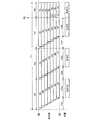
図5は、実施形態2におけるフィールドシーケンシャル制御の一例を示すタイムチャートである。実施形態2は、実施形態1におけるリセットタイミングBSでのリセットとは異なりリセットタイミングWSで全画素Pixにおける光の散乱度合いを所定値以上にするようなリセットが行われる。尚、実施形態2は、輝度補正期間FI4における画素Pixへの階調信号の出力制御内容が実施形態1と異なる点を除いて実施形態1と同様である。 FIG. 5 is a time chart showing an example of field sequential control in the second embodiment. In the second embodiment, unlike the reset in the reset timing BS in the first embodiment, the reset timing WS is used to reset the light scattering degree in all pixel Pix to a predetermined value or more. The second embodiment is the same as the first embodiment except that the output control content of the gradation signal to the pixel Pix during the luminance correction period FI4 is different from that of the first embodiment.
実施形態2では、フィールド期間FI3の後にリセットタイミングWSが設けられ、リセットタイミングWSの後に輝度補正期間FI4が設けられる。リセットタイミングWSには、表示部7の全画素Pixが光の散乱度合いを所定値以上にするようリセットされ、る。具体的には、例えば走査回路9から全走査線5に駆動信号が与えられ、全信号線4が所定値以上の階調値(例えば、8ビット階調制御の場合、255等の最高階調)に対応する電位となるよう信号出力回路8が動作することで、表示部7の全画素Pixがリセットされる。 In the second embodiment, the reset timing WS is provided after the field period FI3, and the brightness correction period FI4 is provided after the reset timing WS. At the reset timing WS, all the pixels Pix of the
実施形態2における輝度補正期間FI4中は、輝度補正を行うための階調信号がライン単位で各画素Pixに書き込まれる点で実施形態1の輝度補正期間FI4と同様だが、具体的な階調信号の出力制御内容が実施形態1と異なる。具体的には、リセットタイミングWSによって全画素Pixに与えられた最高の階調値よりも低い階調値に対応する階調信号が一部のラインの画素Pixに与えられてもよい。 During the luminance correction period FI4 in the second embodiment, the gradation signal for performing the luminance correction is written to each pixel Pix in line units, which is the same as the luminance correction period FI4 of the first embodiment, but a specific gradation signal. The output control content of is different from that of the first embodiment. Specifically, a gradation signal corresponding to a gradation value lower than the highest gradation value given to all pixel Pix by the reset timing WS may be given to the pixel Pix of some lines.
より具体的には、図5では、画像表示期間中にライン画像R7,G7,B7が与えられていた光源11により近い側の走査線5と接続されている画素Pixに対して、輝度補正期間FI4中にライン画像B1が与えられ、輝度補正期間FI4の終了まで保持されている。また、光源11からより遠い側の走査線5と接続されている画素Pixに対して、リセットタイミングBSの直後にライン画像W1が与えられ、輝度補正期間FI4の終了まで保持されている。一方、また、光源11との位置関係でライン画像B1が与えられるラインと画像表示期間中にライン画像R1,G1,B1が与えられていたラインの間に位置するライン、例えば、画像表示期間中にライン画像R6,G6,B6が与えられていた光源11により近い側の走査線5と接続されている画素Pixに対して、ライン画像B1が与えられるタイミングよりも後のタイミングにライン画像B2が与えられ、輝度補正期間FI4の終了まで保持されている。また、リセットタイミングWSの直後に第1光源11Rと第2光源11Gと第3光源11Bを全て点灯させ、輝度補正期間FI4が終了すると光源11は消灯する。 More specifically, in FIG. 5, the brightness correction period is provided for the pixel Pix connected to the scanning line 5 on the side closer to the
ライン画像B1又はライン画像B2が与えられるラインでは、次のフレームのライン画像B1又はライン画像B2が与えられるまでの期間、リセットタイミングWSによって与えられた電位が画素Pixで保持される。また、ライン画像B1及びライン画像B2が与えられないラインでは、輝度補正期間FI4中、リセットタイミングWSによって与えられた電位が画素Pixで保持される。図4等では、リセットタイミングWSによって与えられた電位が保持される期間を白期間Wとして示している。 In the line to which the line image B1 or the line image B2 is given, the potential given by the reset timing WS is held by the pixel Pix until the line image B1 or the line image B2 of the next frame is given. Further, in the line where the line image B1 and the line image B2 are not given, the potential given by the reset timing WS is held by the pixel Pix during the luminance correction period FI4. In FIG. 4 and the like, the period during which the potential given by the reset timing WS is held is shown as the white period W.
なお、ライン画像B1と、ライン画像B2とは、同じ電位の階調信号であってもよいし、それぞれ電位の異なる階調信号であってもよい。ただし、ライン画像B1及びライン画像B2は、リセットタイミングWSによって全画素Pixに与えられた所定値以上の階調値よりも低い階調値に対応するものである。実施形態1では、例えば、ライン画像W1、ライン画像W2及びライン画像W3は、例えば画素信号の最大の階調値に対応する電位を画素Pixに与えるための階調信号である。ライン画像B1とライン画像B2とがそれぞれ電位の異なる階調信号である場合、ライン画像B2による画素Pixの光の散乱度合いがライン画像B1による画素Pixの光の散乱度合い以上になるよう電位が制御される。 The line image B1 and the line image B2 may be gradation signals having the same potential, or may be gradation signals having different potentials. However, the line image B1 and the line image B2 correspond to a gradation value lower than a predetermined value or more given to all pixels Pix by the reset timing WS. In the first embodiment, for example, the line image W1, the line image W2, and the line image W3 are gradation signals for giving the pixel Pix a potential corresponding to the maximum gradation value of the pixel signal, for example. When the line image B1 and the line image B2 are gradation signals having different potentials, the potential is controlled so that the degree of light scattering of the pixel Pix by the line image B2 is equal to or greater than the degree of light scattering of the pixel Pix by the line image B1. Will be done.
ライン画像B1又はライン画像B2が与えられるラインは、ライン画像B1又はライン画像B2が与えられるまでの期間、リセットタイミングWSによって与えられた電位によって画素Pixによる光の散乱度合いが所定値以上の状態に制御されている。従って、輝度補正期間FI4中の全期間で見た場合、ライン画像B1が与えられるラインは、リセットタイミングWSによって与えられた電位によって画素Pixによる光の散乱度合いが所定値以上の状態である時間が最も短く、ライン画像B2が与えられるライン及びライン画像B1もライン画像B2も与えられないラインよりも低輝度になる。また、ライン画像B2が与えられるラインは、ライン画像B1が与えられるラインに比してリセットタイミングWS時に与えられた電位によって画素Pixによる光の散乱度合いが所定値以上の状態である時間が長く、ライン画像B1が与えられるラインよりも高輝度になる。また、ライン画像B1もライン画像B2も与えられないラインは、ライン画像B1又はライン画像B2が与えられるラインに比してリセットタイミングWSによって与えられた電位によって画素Pixによる光の散乱度合いが所定値以上の状態である時間が長く、ライン画像B1又はライン画像B2が与えられるラインよりも高輝度になる。このように、光源11から相対的に遠いラインの輝度補正期間FI4中における光の散乱期間を、光源11に相対的に近いラインよりの輝度補正期間FI4中における光の散乱期間よりも長くすることで、光源11から相対的に遠いラインの輝度補正期間FI4中の輝度の総計を、光源11に相対的に近いラインの輝度補正期間FI4中における輝度の総計よりも高くすることができる。従って、実施形態2でも、実施形態1と同様、画像表示期間中における各ラインの光源11との相対的な距離差による輝度差(例えば、図3の曲線D参照)を輝度補正期間FI4中に補正し(例えば、図3の曲線E参照)、当該輝度差を低減することができる。尚、光の散乱度合いを所定値以上とするために、画素Pixには例えば画素信号の最大階調に対応する電圧が供給される。 In the line to which the line image B1 or the line image B2 is given, the degree of light scattering by the pixel Pix is set to a predetermined value or more by the potential given by the reset timing WS during the period until the line image B1 or the line image B2 is given. It is controlled. Therefore, when viewed over the entire period during the luminance correction period FI4, the line to which the line image B1 is given is the time during which the degree of light scattering by the pixel Pix is equal to or higher than a predetermined value due to the potential given by the reset timing WS. It is the shortest and has lower brightness than the line to which the line image B2 is given and the line to which neither the line image B1 nor the line image B2 is given. Further, the line to which the line image B2 is given has a longer time in which the degree of light scattering by the pixel Pix is equal to or higher than a predetermined value due to the potential given at the reset timing WS as compared with the line to which the line image B1 is given. The line image B1 has a higher brightness than the given line. Further, in the line where neither the line image B1 nor the line image B2 is given, the degree of light scattering by the pixel Pix is a predetermined value due to the potential given by the reset timing WS as compared with the line to which the line image B1 or the line image B2 is given. The time in the above state is long, and the brightness becomes higher than that of the line to which the line image B1 or the line image B2 is given. In this way, the light scattering period in the brightness correction period FI4 of the line relatively far from the
また、実施形態2でも、輝度補正期間FI4中に複数ラインに対して同一のライン画像が書き込まれるタイミングがある。具体的には、図5で例示するように、画像表示期間中にライン画像R5,G5,B5又はライン画像R6,G6,B6が与えられていた2ラインの画素Pixに対してライン画像B1よりも後のタイミングでライン画像B2が与えられ、輝度補正期間FI4の終了まで保持される。係るライン画像B2を書き込む際に走査回路9から出力される駆動信号は、当該2ラインの走査線5に対して同一タイミングで与えられる。以上、特筆した点を除いて、実施形態2は、実施形態1と同様である。 Further, also in the second embodiment, there is a timing in which the same line image is written for a plurality of lines during the luminance correction period FI4. Specifically, as illustrated in FIG. 5, from the line image B1 with respect to the two-line pixel Pix to which the line image R5, G5, B5 or the line image R6, G6, B6 was given during the image display period. The line image B2 is given at a later timing, and is held until the end of the luminance correction period FI4. The drive signal output from the
実施形態2によれば、実施形態1と同様の効果を得られる。 According to the second embodiment, the same effect as that of the first embodiment can be obtained.
(実施形態3)
以下、図6を参照して実施形態3の表示装置について説明する。実施形態3の説明に係り、実施形態2と同様の構成については同じ符号を付して説明を省略する。(Embodiment 3)
Hereinafter, the display device of the third embodiment will be described with reference to FIG. Regarding the description of the third embodiment, the same reference numerals are given to the same configurations as those of the second embodiment, and the description thereof will be omitted.
図6は、実施形態3におけるフィールドシーケンシャル制御の一例を示すタイムチャートである。実施形態1及び実施形態2では、各書込期間FI11,FI21,FI31中に光源11から遠い側から近い側に向かって走査線5が順次走査されるよう走査回路9から走査線5へ駆動信号が出力されていたが、実施形態3では、図6に示すように、各書込期間FI11,FI21,FI31中に光源11に近い側から遠い側に向かって走査線5が順次走査されるよう走査回路9から走査線5へ駆動信号が出力される。 FIG. 6 is a time chart showing an example of field sequential control in the third embodiment. In the first and second embodiments, a drive signal is sent from the
輝度補正期間FI4には、光源11に近い側に比して光源11から遠い側の輝度をより高める制御が行われる。従って、実施形態3では、実施形態2と異なり、ライン画像B1が与えられるラインが、画像表示期間中にライン画像R1,G1,B1が与えられていた光源11により近い側の走査線5と接続されている画素Pixになる。また、ライン画像B2が与えられるラインが、画像表示期間中にライン画像R2,G2,B2が与えられていた画素Pix及びライン画像R3,G3,B3が与えられていた画素Pixになる。以上、特筆した点を除いて、実施形態3は、実施形態2と同様である。 During the brightness correction period FI4, control is performed to further increase the brightness on the side far from the
実施形態3によれば、画像表示期間中における走査方向が光源11に近い側(走査線5a側)から遠い側(走査線5b側)に向かう方向であり、画像表示期間と輝度補正期間FI4との間に液晶3による散乱度合いが所定値以上に設定されるタイミング(リセットタイミングWS)が設定され、当該タイミング後に液晶による散乱度合いが所定値以下に設定される再設定の順序が一側面側から一側面の反対側へ向かう順序である。これによって、再設定の順序によって、一側面の反対側に近いほど液晶による光の散乱時間が長くなるように輝度補正期間FI4の表示パネル(液晶表示パネルP)を制御することができる。また、画像表示期間中の書込期間FI11,FI21,FI31における走査方向と、輝度補正期間FI4中の書込期間における走査方向とを統一できる。従って、より簡便な制御によって表示パネルと光源11との位置関係による画像の輝度分布の偏りを低減できる。尚、光の散乱度合いを所定値以上とするために、画素Pixには例えば画素信号の最大階調に対応する電圧が供給される。 According to the third embodiment, the scanning direction during the image display period is from the side closer to the light source 11 (scanning
(変形例)
以下、図7及び図8を参照して、実施形態1の変形例について説明する。変形例の説明に係り、実施形態1と同様の構成については同じ符号を付して説明を省略する。(Modification example)
Hereinafter, a modified example of the first embodiment will be described with reference to FIGS. 7 and 8. Regarding the description of the modified example, the same reference numerals are given to the same configurations as those in the first embodiment, and the description thereof will be omitted.
(変形例1)
図7は、変形例1におけるフィールドシーケンシャル制御の一例を示すタイムチャートである。図7に示す例では、実施形態1に係る説明で参照していた図4と異なり、保持期間FI12中に第1光源11Rが非点灯になっている。すなわち、変形例1では、2色の光源(例えば、第2光源11G及び第3光源11B)が点灯するよう光源装置Lの制御が行われる。(Modification example 1)
FIG. 7 is a time chart showing an example of field sequential control in the first modification. In the example shown in FIG. 7, unlike FIG. 4 referred to in the description according to the first embodiment, the first
変形例1のように2色が点灯するよう光源装置Lの制御が行われる場合、輝度補正期間FI4中に表示部7に照射される光は、当該2色の光の合成光である。図7に示す例の場合、画像表示期間中に第2光源11G及び第3光源11Bが点灯する。従って、光源装置Lは、輝度補正期間FI4中に第2光源11G及び第3光源11Bを点灯させることで、緑色(G)の光と青色(B)の光の合成光としてシアン(C)の光を発する。 When the light source device L is controlled so that the two colors are lit as in the first modification, the light emitted to the
なお、フィールド期間FI3と輝度補正期間FI4との間にリセットタイミングBSによるリセットタイミングが設けられること及び輝度補正期間FI4中における階調信号の制御については、変形例1と実施形態1との間に差異はない。具体的には、図4においてライン画像W1、ライン画像W2、ライン画像W3として図示されていた輝度補正期間FI4中の各ラインの階調信号の記載が図7ではライン画像C1、ライン画像C2、ライン画像C3として図示されているが、これは、輝度補正期間FI4中に照射される光が白色光からシアン(C)の光になったことで画素Pixが白色光でなくシアン(C)の光を散乱させる状態であることを示す記載であって、階調信号の制御の変更を示す記載でない。画素Pixにライン画像C1、ライン画像C2、ライン画像C3を与える階調信号の制御は、画素Pixにライン画像W1、ライン画像W2、ライン画像W3を与える階調信号の制御と同様である。 Regarding the fact that the reset timing by the reset timing BS is provided between the field period FI3 and the luminance correction period FI4 and the control of the gradation signal during the luminance correction period FI4, it is between the first modification and the first embodiment. There is no difference. Specifically, the description of the gradation signal of each line in the brightness correction period FI4 shown as the line image W1, the line image W2, and the line image W3 in FIG. 4 is described in FIG. 7, the line image C1, the line image C2, and the line image C2. Although illustrated as a line image C3, this is because the light emitted during the brightness correction period FI4 has changed from white light to cyan (C) light, so that the pixel Pix is not white light but cyan (C). It is a description indicating that the light is scattered, and is not a description indicating a change in the control of the gradation signal. The control of the gradation signal for giving the line image C1, the line image C2, and the line image C3 to the pixel Pix is the same as the control of the gradation signal for giving the line image W1, the line image W2, and the line image W3 to the pixel Pix.
(変形例2)
図8は、変形例2におけるフィールドシーケンシャル制御の一例を示すタイムチャートである。図8に示す例では、実施形態1に係る説明で参照していた図4と異なり、保持期間FI12中に第2光源11G及び第3光源11Bが非点灯になっている。すなわち、変形例2では、1色の光源(例えば、第1光源11R)が点灯するよう光源装置Lの制御が行われる。(Modification 2)
FIG. 8 is a time chart showing an example of field sequential control in the second modification. In the example shown in FIG. 8, unlike FIG. 4 referred to in the description according to the first embodiment, the second
変形例2のように1色が点灯するよう光源装置Lの制御が行われる場合、輝度補正期間FI4中に表示部7に照射される光は、当該1色の光である。図8に示す例の場合、画像表示期間中に第1光源11Rが点灯する。従って、光源装置Lは、輝度補正期間FI4中に第1光源11Rを点灯させる。 When the light source device L is controlled so that one color is lit as in the second modification, the light emitted to the
なお、フィールド期間FI3と輝度補正期間FI4との間にリセットタイミングBSによるリセットタイミングが設けられること及び輝度補正期間FI4中における階調信号の制御については、変形例2と実施形態1との間に差異はない。具体的には、図4においてライン画像W1、ライン画像W2、ライン画像W3として図示されていた輝度補正期間FI4中の各ラインの階調信号の記載が図7ではライン画像Ra、ライン画像Rb、ライン画像Rcとして図示されているが、これは、輝度補正期間FI4中に照射される光が白色光から赤色(R)の光になったことで画素Pixが白色光でなく赤色(R)の光を散乱させる状態であることを示す記載であって、階調信号の制御の変更を示す記載でない。画素Pixにライン画像Ra、ライン画像Rb、ライン画像Rcを与える階調信号の制御は、画素Pixにライン画像W1、ライン画像W2、ライン画像W3を与える階調信号の制御と同様である。 Regarding the fact that the reset timing by the reset timing BS is provided between the field period FI3 and the luminance correction period FI4 and the control of the gradation signal during the luminance correction period FI4, it is between the second modification and the first embodiment. There is no difference. Specifically, the description of the gradation signal of each line in the brightness correction period FI4 shown as the line image W1, the line image W2, and the line image W3 in FIG. 4 is shown in FIG. 7 as the line image Ra, the line image Rb, and so on. Although it is shown as a line image Rc, this is because the light emitted during the brightness correction period FI4 changes from white light to red (R) light, so that the pixel Pix is not white light but red (R). It is a description indicating that the light is scattered, and is not a description indicating a change in the control of the gradation signal. The control of the gradation signal for giving the line image Ra, the line image Rb, and the line image Rc to the pixel Pix is the same as the control of the gradation signal for giving the line image W1, the line image W2, and the line image W3 to the pixel Pix.
なお、変形例1における2色の光は緑色(G)の光と青色(B)の光に限られるものでない。例えば、2色の光を赤色(R)の光と緑色(G)の光とした場合、合成光はイエロー(Y)になる。また、2色の光を赤色(R)の光と青色(B)の光とした場合、合成光はマゼンタ(M)になる。また、変形例2における1色の光は赤色(R)に限られるものでなく、他の色であってもよい。例えば、変形例2における1色の光は白色光であってもよい。 The two-color light in the first modification is not limited to the green (G) light and the blue (B) light. For example, when the two colors of light are red (R) light and green (G) light, the combined light is yellow (Y). Further, when the two colors of light are red (R) light and blue (B) light, the combined light becomes magenta (M). Further, the light of one color in the second modification is not limited to red (R), and may be another color. For example, the one-color light in the second modification may be white light.
また、光源11から発せられる光の色は、赤色(R)、緑色(G)、青色(B)及びその合成色に限られるものでない。すなわち、光源装置Lが備える光源11を構成する発光素子から発せられる光の色を他の色にしてもよい。また、光源11を構成する発光素子から照射可能な光の色は3色(及びその一部又は全部の合成色)に限られるものでなく、2色以下であってもよいし、4色以上であってもよい。 Further, the color of the light emitted from the
また、実施形態2,3についても、変形例を適用可能である。すなわち、実施形態2,3における画像表示期間が変形例1,2のような画像表示期間である場合、図5及び図6の輝度補正期間FI4中における光源11からの光を、変形例1,2の輝度補正期間FI4中における光源11中における光源11からの光に置換することで、実施形態2,3に変形例を適用できる。 Further, the modified examples can also be applied to the second and third embodiments. That is, when the image display period in the second and third embodiments is the image display period as in the first and second modifications, the light from the
また、図7及び図8では光源11が非点灯であるフィールド期間の書込期間及び保持期間が設けられているが、このような光源11が非点灯であるフィールド期間は、フレーム期間FLから省略可能である。省略されたフィールド期間の時間を他のフィールド期間の一部又は全部に割り当てて他のフィールド期間の時間をより長くしてもよいし、省略されたフィールド期間の分だけフレーム期間FLの時間を短縮してもよい。 Further, in FIGS. 7 and 8, a writing period and a holding period for a field period in which the
また、輝度補正期間は、表示部7の輝度分布の均一化だけでなく、表示部7全体の輝度向上にも利用可能である。 Further, the luminance correction period can be used not only for making the luminance distribution of the
図9は、輝度補正期間FI4における光源11の点灯時間が関係する変数(Tw/T2)と表示部7の輝度指標との対応関係の一例を示すグラフである。輝度指標とは、当該各実施形態と同一の時間を有するフレーム期間FLにおいて輝度補正期間FI4を設けず、フレーム期間FLの時間を全て画像表示期間に割り当てた比較例における表示部7全体の輝度を基準(1)として表示部7全体の輝度を評価した値である。 FIG. 9 is a graph showing an example of the correspondence between the variable (Tw / T2) related to the lighting time of the
図4から図6を参照して説明した各実施形態の保持期間FI12,FI22,FI32における光源11の点灯時間の総計をT3とする。また、各実施形態の輝度補正期間FI4における光源11の点灯時間をTwとする。また、比較例における保持期間FI12,FI22,FI32の各々における光源11の点灯時間の総計をT2とする。この場合、Tw及びT2を用いてT3を表すと、式(1)のようになる。
T3=T2−{(1/3)*(T1+Tw)}…(1)Let T3 be the total lighting time of the
T3 = T2-{(1/3) * (T1 + Tw)} ... (1)
比較例における書込期間FI11,FI21,FI31の時間の総計をT1とする。また、比較例において第1光源11R、第2光源11G、第3光源11Bを全点灯した場合の輝度を1とする。この場合、各実施形態の輝度補正期間FI4における光源11の輝度L(3)の総計は、式(2)のようになる。
L(3)=(T3/T2)+{[3×(Tw/3)]/T2}=1−{(T1−2Tw)/3T2}…(2)Let T1 be the total time of the writing periods FI11, FI21, and FI31 in the comparative example. Further, in the comparative example, the brightness when the first
L (3) = (T3 / T2) + {[3 × (Tw / 3)] / T2} = 1-{(T1-2Tw) / 3T2} ... (2)
式(2)において、Tw/T2をxとすると、式(2)は、式(3)のように表せる。ここで、x=Tw/T2を横軸とし、表示部7の輝度指標を縦軸とすると、式(3)は、図9に示すグラフの線L1のように表せる。
L1:L(3)=1−{(T1−2T2x)/3T2}…(3)In the formula (2), where Tw / T2 is x, the formula (2) can be expressed as the formula (3). Here, assuming that x = Tw / T2 is the horizontal axis and the luminance index of the
L1: L (3) = 1-{(T1-2T2x) / 3T2} ... (3)
また、式(1)から式(3)に係る考え方と同様の考え方で、変形例1のように輝度補正期間FI4中に照射される合成光が2色の光の合成光である場合の輝度補正期間FI4における光源11の輝度L(2)を導出すると、式(4)のように表せる。式(4)は、図9に示すグラフの線L2のように表せる。
L2:L(2)=1−{(T1−T2x)/3T2}…(4)Further, in the same way as the way of thinking related to the formulas (1) to (3), the brightness when the composite light irradiated during the brightness correction period FI4 is the composite light of two colors of light as in the first modification. When the brightness L (2) of the
L2: L (2) = 1-{(T1-T2x) / 3T2} ... (4)
図9は、T1=T2=2.77ミリ秒[ms]である場合のグラフである。図9によれば、x=Tw/T2が0.5以上である場合、各実施形態の表示部7の輝度指標は1以上になる。従って、Tw/T2が0.5以上になるように輝度補正期間を設けることで、表示部7全体の輝度向上を図れる。なお、T1=T2=2.77ミリ秒[ms]である場合に限られず、T1,T2の値は適宜変更可能である。 FIG. 9 is a graph when T1 = T2 = 2.77 milliseconds [ms]. According to FIG. 9, when x = Tw / T2 is 0.5 or more, the luminance index of the
なお、実施形態1,2,3を適宜組み合わせて輝度補償を行ってもよい。例えば、タイミングコントローラ13の制御下で光源駆動回路12が輝度補正期間FI4に点灯させる第1光源11R、第2光源11G、第3光源11Bの各々の点灯量は、画像表示期間に点灯させた第1光源11R、第2光源11G、第3光源11Bの各々の点灯量と同じになるような制御をしてもよい。 Luminance compensation may be performed by appropriately combining the first, second, and third embodiments. For example, the lighting amounts of the first
また、光源装置Lは、液晶表示パネルPを照明可能であればよく、その具体的な配置については適宜変更可能である。例えば、光源装置Lは、フロントライトであってもよい。また、液晶表示パネルPは、高分子分散型液晶を利用した液晶表示パネルに限られるものでなく、例えば、FSCを適用可能な透過型、半透過型又は反射型の表示パネル等、他の形態の表示パネルであってもよい。透過型の表示パネルである場合、光源装置Lは、表示面の背面側に設けられる。 Further, the light source device L may illuminate the liquid crystal display panel P, and its specific arrangement can be appropriately changed. For example, the light source device L may be a front light. Further, the liquid crystal display panel P is not limited to a liquid crystal display panel using a polymer-dispersed liquid crystal, and has other forms such as a transmissive type, transflective type, or reflective type display panel to which FSC can be applied. It may be a display panel of. In the case of a transmissive display panel, the light source device L is provided on the back side of the display surface.
また、本実施形態において述べた態様によりもたらされる他の作用効果について本明細書記載から明らかなもの、又は当業者において適宜想到し得るものについては、当然に本発明によりもたらされるものと解される。 Further, it is understood that those which are clear from the description of the present specification or which can be appropriately conceived by those skilled in the art are naturally brought about by the present invention as other effects brought about by the aspects described in the present embodiment. ..
5,5a,5b 走査線
7 表示部
8 信号出力回路
9 走査回路
11 光源
11R 第1光源
11G 第2光源
11B 第3光源
12 光源駆動回路
13 タイミングコントローラ
15 入力回路
100 表示装置
P 液晶表示パネル
L 光源装置5,5a,
Claims (11)
Translated fromJapanese前記表示パネルの一側面側から光を照射する光源とを備え、
1つの前記フレーム画像に対して割り当てられる1フレーム期間は、画像表示期間と輝度補正期間を含み、
前記輝度補正期間における前記表示パネルの輝度の総計は、前記一側面の反対側に近いほど高い
表示装置。A display panel in which a polymer-dispersed liquid crystal is enclosed between two opposing substrates to display a frame image by arranging a plurality of line images in the scanning direction.
A light source that irradiates light from one side surface of the display panel is provided.
The one frame period allocated to one frame image includes an image display period and a brightness correction period.
A display device in which the total brightness of the display panel during the brightness correction period is higher as it is closer to the opposite side of the one side surface.
請求項1に記載の表示装置。The display device according to claim 1, wherein the display panel during the brightness correction period has a higher degree of light scattering by the polymer-dispersed liquid crystal as it is closer to the opposite side of the one side surface.
請求項1又は2に記載の表示装置。The display device according to claim 1 or 2, wherein the display panel during the brightness correction period has a longer light scattering time by the polymer-dispersed liquid crystal as it is closer to the opposite side of the one side surface.
前記サブフレーム期間は、前記ライン画像の書込期間と前記光源からの光が照射される照射期間とを含み、
前記輝度補正期間に照射される光は、前記光源からの光の合成色である
請求項1から3のいずれか一項に記載の表示装置。The image display period includes a predetermined number of subframe periods corresponding to the number of colors of light from the light source.
The subframe period includes a writing period of the line image and an irradiation period in which light from the light source is irradiated.
The display device according to any one of claims 1 to 3, wherein the light emitted during the luminance correction period is a composite color of light from the light source.
前記輝度補正期間に前記光源から照射される光は、白色光である
請求項4に記載の表示装置。The light source includes a first light source that emits red light, a second light source that emits green light, and a third light source that emits blue light.
The display device according to claim 4, wherein the light emitted from the light source during the luminance correction period is white light.
請求項5に記載の表示装置。The lighting amounts of the first light source, the second light source, and the third light source that are lit during the brightness correction period are the respective lighting amounts of the first light source, the second light source, and the third light source during the image display period. The display device according to claim 5, which is the same as the lighting amount.
請求項1から6のいずれか一項に記載の表示装置。The item according to any one of claims 1 to 6, wherein a reset timing in which the degree of light scattering by the polymer-dispersed liquid crystal is set to a predetermined value or less is provided between the image display period and the brightness correction period. Display device.
請求項7に記載の表示装置。The scanning direction during the image display period is the direction from the opposite side of the one side surface to the one side surface side, and the degree of scattering by the polymer-dispersed liquid crystal is set to a predetermined value or more after the reset timing. The display device according to claim 7, wherein the order is from the opposite side of the one side surface to the one side surface side.
請求項1から6のいずれか一項に記載の表示装置。A timing is set between the image display period and the brightness correction period in which the degree of scattering by the polymer-dispersed liquid crystal is set to a predetermined value or more, and after the timing, the degree of scattering by the polymer-dispersed liquid crystal is set to a predetermined value. The display device according to any one of claims 1 to 6, wherein the resetting order set below is an order from the one side surface side to the opposite side of the one side surface.
請求項9に記載の表示装置。The display device according to claim 9, wherein the scanning direction during the image display period is a direction from the one side surface side to the opposite side of the one side surface side.
請求項8から10のいずれか一項に記載の表示装置。The display device according to any one of claims 8 to 10, wherein at least a part of the display panel controls the polymer-dispersed liquid crystal in units of a plurality of lines at the time of resetting.
Priority Applications (2)
| Application Number | Priority Date | Filing Date | Title |
|---|---|---|---|
| JP2019128616AJP7222835B2 (en) | 2019-07-10 | 2019-07-10 | Display device |
| US16/923,223US11158268B2 (en) | 2019-07-10 | 2020-07-08 | Display device |
Applications Claiming Priority (1)
| Application Number | Priority Date | Filing Date | Title |
|---|---|---|---|
| JP2019128616AJP7222835B2 (en) | 2019-07-10 | 2019-07-10 | Display device |
Publications (2)
| Publication Number | Publication Date |
|---|---|
| JP2021015153Atrue JP2021015153A (en) | 2021-02-12 |
| JP7222835B2 JP7222835B2 (en) | 2023-02-15 |
Family
ID=74101807
Family Applications (1)
| Application Number | Title | Priority Date | Filing Date |
|---|---|---|---|
| JP2019128616AActiveJP7222835B2 (en) | 2019-07-10 | 2019-07-10 | Display device |
Country Status (2)
| Country | Link |
|---|---|
| US (1) | US11158268B2 (en) |
| JP (1) | JP7222835B2 (en) |
Families Citing this family (2)
| Publication number | Priority date | Publication date | Assignee | Title |
|---|---|---|---|---|
| JP7526070B2 (en)* | 2020-10-12 | 2024-07-31 | 株式会社ジャパンディスプレイ | Display device |
| JP2024073087A (en)* | 2022-11-17 | 2024-05-29 | 株式会社ジャパンディスプレイ | Display device |
Citations (4)
| Publication number | Priority date | Publication date | Assignee | Title |
|---|---|---|---|---|
| WO2010035562A1 (en)* | 2008-09-25 | 2010-04-01 | シャープ株式会社 | Light quantity control device, backlight unit, liquid crystal display panel, and liquid crystal display device |
| JP2017156491A (en)* | 2016-03-01 | 2017-09-07 | 株式会社ジャパンディスプレイ | Display device |
| JP2018049089A (en)* | 2016-09-20 | 2018-03-29 | 株式会社ジャパンディスプレイ | Display device |
| JP2018194592A (en)* | 2017-05-12 | 2018-12-06 | 株式会社ジャパンディスプレイ | Display device |
Family Cites Families (18)
| Publication number | Priority date | Publication date | Assignee | Title |
|---|---|---|---|---|
| EP2653913B1 (en)* | 2010-12-17 | 2018-08-15 | Sony Corporation | Illumination device, display device and three-dimensional display device |
| JP5991053B2 (en)* | 2011-10-04 | 2016-09-14 | ソニー株式会社 | Display device and lighting device |
| JP5929083B2 (en)* | 2011-10-04 | 2016-06-01 | ソニー株式会社 | Display device |
| JP5817989B2 (en)* | 2011-10-05 | 2015-11-18 | ソニー株式会社 | LIGHTING DEVICE, DISPLAY DEVICE, AND ELECTRONIC DEVICE |
| JP2014102295A (en)* | 2012-11-16 | 2014-06-05 | Sony Corp | Display device, display method and recording medium |
| CN103327275B (en)* | 2013-05-08 | 2016-06-29 | 深圳市绎立锐光科技开发有限公司 | Display uniformity compensation method, optic modulating device, signal processor and optical projection system |
| WO2015186593A1 (en)* | 2014-06-04 | 2015-12-10 | シャープ株式会社 | Display device |
| JP2016051002A (en) | 2014-08-29 | 2016-04-11 | 株式会社ジャパンディスプレイ | Display device, light correction device, and light correction method |
| JP2016057338A (en)* | 2014-09-05 | 2016-04-21 | 株式会社ジャパンディスプレイ | Display device and light source device |
| JP6364335B2 (en)* | 2014-12-04 | 2018-07-25 | 株式会社ジャパンディスプレイ | Display device |
| US9804317B2 (en)* | 2015-02-06 | 2017-10-31 | Japan Display Inc. | Display apparatus |
| JP2017076006A (en)* | 2015-10-13 | 2017-04-20 | 株式会社ジャパンディスプレイ | Display device |
| JP6671940B2 (en)* | 2015-12-07 | 2020-03-25 | 株式会社ジャパンディスプレイ | Display device |
| WO2017188347A1 (en)* | 2016-04-28 | 2017-11-02 | シャープ株式会社 | Liquid crystal display device, drive method for liquid crystal panel, setting method for write signal for liquid crystal display device |
| JP6800641B2 (en)* | 2016-07-22 | 2020-12-16 | 株式会社ジャパンディスプレイ | Display device |
| KR102347768B1 (en)* | 2017-04-24 | 2022-01-07 | 삼성디스플레이 주식회사 | Display apparatus and method of driving display panel using the same |
| JP2019082549A (en)* | 2017-10-30 | 2019-05-30 | シャープ株式会社 | Field sequential type image display device and image display method |
| CN109377942B (en)* | 2018-12-24 | 2020-07-03 | 合肥鑫晟光电科技有限公司 | Compensation method, device and display device for display device |
- 2019
- 2019-07-10JPJP2019128616Apatent/JP7222835B2/enactiveActive
- 2020
- 2020-07-08USUS16/923,223patent/US11158268B2/enactiveActive
Patent Citations (4)
| Publication number | Priority date | Publication date | Assignee | Title |
|---|---|---|---|---|
| WO2010035562A1 (en)* | 2008-09-25 | 2010-04-01 | シャープ株式会社 | Light quantity control device, backlight unit, liquid crystal display panel, and liquid crystal display device |
| JP2017156491A (en)* | 2016-03-01 | 2017-09-07 | 株式会社ジャパンディスプレイ | Display device |
| JP2018049089A (en)* | 2016-09-20 | 2018-03-29 | 株式会社ジャパンディスプレイ | Display device |
| JP2018194592A (en)* | 2017-05-12 | 2018-12-06 | 株式会社ジャパンディスプレイ | Display device |
Also Published As
| Publication number | Publication date |
|---|---|
| JP7222835B2 (en) | 2023-02-15 |
| US11158268B2 (en) | 2021-10-26 |
| US20210012726A1 (en) | 2021-01-14 |
Similar Documents
| Publication | Publication Date | Title |
|---|---|---|
| CN102301273B (en) | Display device and display method | |
| US7233304B1 (en) | Liquid crystal display apparatus | |
| US8026893B2 (en) | Liquid crystal display device and apparatus and method for driving the same | |
| JP4331192B2 (en) | Liquid crystal display device and driving method thereof | |
| US20080224986A1 (en) | Color sequential display having backlight timing delay control unit and method thereof | |
| US11302272B2 (en) | Display device, and driving method for the display device for reducing power consumption and improving display effect | |
| WO2007097055A1 (en) | Display | |
| JP2016126337A (en) | Display device and driving method thereof | |
| JP5273391B2 (en) | Liquid crystal display | |
| JP7222835B2 (en) | Display device | |
| US11735132B2 (en) | Display device writes a same image to a predetermined number of lines | |
| JP7404162B2 (en) | display device | |
| JP7287855B2 (en) | Display device | |
| KR101362151B1 (en) | Liquid crystal display and driving method thereof | |
| US11656501B2 (en) | Display device | |
| US10140933B2 (en) | Display apparatus and method for driving display apparatus | |
| WO2022176607A1 (en) | Head-up display | |
| KR20100019186A (en) | Driving apparatus for liquid crystal display device and method for driving the same | |
| JP2007212782A (en) | Method for driving color liquid crystal display device assembly | |
| JP2005115139A (en) | Electro-optic device | |
| JP6985808B2 (en) | Display device and drive method of display device | |
| WO2016059847A1 (en) | Display device | |
| US10032418B2 (en) | Display apparatus | |
| KR100712292B1 (en) | LCD Display | |
| JP2023101535A (en) | Display device and display system |
Legal Events
| Date | Code | Title | Description |
|---|---|---|---|
| A621 | Written request for application examination | Free format text:JAPANESE INTERMEDIATE CODE: A621 Effective date:20220131 | |
| A977 | Report on retrieval | Free format text:JAPANESE INTERMEDIATE CODE: A971007 Effective date:20220930 | |
| A131 | Notification of reasons for refusal | Free format text:JAPANESE INTERMEDIATE CODE: A131 Effective date:20221011 | |
| A521 | Request for written amendment filed | Free format text:JAPANESE INTERMEDIATE CODE: A523 Effective date:20221124 | |
| TRDD | Decision of grant or rejection written | ||
| A01 | Written decision to grant a patent or to grant a registration (utility model) | Free format text:JAPANESE INTERMEDIATE CODE: A01 Effective date:20230117 | |
| A61 | First payment of annual fees (during grant procedure) | Free format text:JAPANESE INTERMEDIATE CODE: A61 Effective date:20230203 | |
| R150 | Certificate of patent or registration of utility model | Ref document number:7222835 Country of ref document:JP Free format text:JAPANESE INTERMEDIATE CODE: R150 |