Movatterモバイル変換


[0]ホーム

URL:


JP2021002546A - Semiconductor laser light source module and semiconductor laser device - Google Patents

Semiconductor laser light source module and semiconductor laser device
Download PDF

Info

Publication number
JP2021002546A
JP2021002546AJP2019114331AJP2019114331AJP2021002546AJP 2021002546 AJP2021002546 AJP 2021002546AJP 2019114331 AJP2019114331 AJP 2019114331AJP 2019114331 AJP2019114331 AJP 2019114331AJP 2021002546 AJP2021002546 AJP 2021002546A
Authority
JP
Japan
Prior art keywords
semiconductor laser
conductor
light source
laser light
electrode
Prior art date
Legal status (The legal status is an assumption and is not a legal conclusion. Google has not performed a legal analysis and makes no representation as to the accuracy of the status listed.)
Granted
Application number
JP2019114331A
Other languages
Japanese (ja)
Other versions
JP7275894B2 (en
Inventor
山田 仁
Hitoshi Yamada
仁 山田
Current Assignee (The listed assignees may be inaccurate. Google has not performed a legal analysis and makes no representation or warranty as to the accuracy of the list.)
Denso Corp
Original Assignee
Denso Corp
Priority date (The priority date is an assumption and is not a legal conclusion. Google has not performed a legal analysis and makes no representation as to the accuracy of the date listed.)
Filing date
Publication date
Application filed by Denso CorpfiledCriticalDenso Corp
Priority to JP2019114331ApriorityCriticalpatent/JP7275894B2/en
Publication of JP2021002546ApublicationCriticalpatent/JP2021002546A/en
Application grantedgrantedCritical
Publication of JP7275894B2publicationCriticalpatent/JP7275894B2/en
Activelegal-statusCriticalCurrent
Anticipated expirationlegal-statusCritical

Links

Images

Landscapes

Abstract

To provide a technique which can supply the current to a laser diode without using a bonding wire in a semiconductor laser light source module and suppress the occurrence of a parasitic inductance.SOLUTION: A semiconductor laser light source module 100 comprises: an end surface emission type laser diode 60 which has a first electrode 64 formed on one surface side of a semiconductor layer 63 including an active layer and a second electrode 62 formed on the other surface side of the active layer; a housing 90 which has a side wall part surrounding the laser diode and a light transmitting part for transmitting the laser light to at least a portion of the side wall part; a first conductor 70 which is in contact with the first electrode; a second conductor 40 which is in contact with the second electrode; a first connection part 70W which is provided on the outer side of the side wall part and electrically connected to the first conductor; and a second connection part 40W which is provided on the outer side of the side wall part and electrically connected to the second conductor.SELECTED DRAWING: Figure 3

Description

Translated fromJapanese

本開示は、半導体レーザ光源モジュールおよび半導体レーザ装置に関する。 The present disclosure relates to a semiconductor laser light source module and a semiconductor laser device.

筐体内に収容されたレーザダイオードの電極と、電源電極とをワイヤボンディングにより電気的に接続されている半導体レーザ光源モジュールが知られている(例えば、特許文献1)。 A semiconductor laser light source module in which an electrode of a laser diode housed in a housing and a power supply electrode are electrically connected by wire bonding is known (for example, Patent Document 1).

特開2013−65600号公報Japanese Unexamined Patent Publication No. 2013-65600

従来の技術では、ワイヤを流れる電流によって寄生インダクタンスが発生するといった問題がある。 In the conventional technique, there is a problem that a parasitic inductance is generated by a current flowing through a wire.

本開示は、以下の形態として実現することが可能である。 The present disclosure can be realized in the following forms.

本開示の一形態によれば、半導体レーザ光源モジュール(100,100b,100c)が提供される。この半導体レーザ光源モジュールは、活性層を含む半導体層(63)の一方の面側に形成された第一電極(64)と、前記活性層の他方の面側に形成された第二電極(62)とを備える端面出射型のレーザダイオード(60)と、前記レーザダイオードを囲む側壁部(90W)を有して前記側壁部のうち少なくとも一部にレーザ光を透過する透光部(92)を備える筐体(90)と、前記第一電極に当接される第一導電体(70,70b)と、前記第二電極に当接される第二導電体(40,40b)と、前記側壁部の外部側に設けられ、前記第一導電体と電気的に接続される第一接続部と、前記側壁部の外部側に設けられ、前記第二導電体と電気的に接続される第二接続部と、を備える。 According to one embodiment of the present disclosure, a semiconductor laser light source module (100, 100b, 100c) is provided. This semiconductor laser light source module includes a first electrode (64) formed on one surface side of a semiconductor layer (63) including an active layer and a second electrode (62) formed on the other surface side of the active layer. ), And a translucent portion (92) having a side wall portion (90 W) surrounding the laser diode and transmitting laser light to at least a part of the side wall portion. A housing (90) to be provided, a first conductor (70, 70b) abutting on the first electrode, a second conductor (40, 40b) abutting on the second electrode, and the side wall. A first connection portion provided on the outer side of the portion and electrically connected to the first conductor, and a second connection portion provided on the outer side of the side wall portion and electrically connected to the second conductor. It is provided with a connection part.

この形態の半導体レーザ光源モジュールによれば、正極側となる第一導電体と、レーザダイオードの第一電極とが当接されて電気的に接続されるとともに、負極側となる第二導電体と、第二電極とが当接されて電気的に接続される。半導体レーザ光源モジュールは、側壁部の外部側に第一接続部と、第二接続部とを備え、半導体レーザ装置の回路基板上に実装可能に構成される。したがって、ボンディングワイヤを用いることなくレーザダイオードに電流を供給でき、寄生インダクタンスの発生を抑制することができる。 According to the semiconductor laser light source module of this form, the first conductor on the positive electrode side and the first electrode of the laser diode are brought into contact with each other and electrically connected, and the second conductor on the negative electrode side is formed. , The second electrode is abutted and electrically connected. The semiconductor laser light source module is provided with a first connection portion and a second connection portion on the outer side of the side wall portion, and is configured to be mountable on a circuit board of a semiconductor laser device. Therefore, the current can be supplied to the laser diode without using the bonding wire, and the generation of parasitic inductance can be suppressed.

本開示の一形態によれば、半導体レーザ光源モジュール(200,200e)が提供される。この半導体レーザ光源モジュールは、活性層を含む半導体層(163)の一方の面側に形成された第一電極(164)と、前記活性層の他方の面側に形成された第二電極(162)とを備える端面出射型のレーザダイオード(160)と、前記レーザダイオードを囲む側壁部(190W)を有し、前記側壁部のうち少なくとも一部にレーザ光を透過する透光部(192)を備える筐体(190)と、前記第一電極と電気的に接続され、前記レーザダイオードを駆動する平板状のLDドライバ(110)と、前記レーザダイオードを挟んで前記LDドライバの一方の面側と対向するように配され、前記第二電極に当接されて前記レーザダイオードと電気的に接続される導電体(170)と、前記LDドライバの他方の面側に当接されるセラミック製の基台部(130,130e)と、前記筐体の外部側に配置される第一電極パッド(134)であって、前記LDドライバと電気的に接続される第一電極パッドと、前記筐体の外部側に配置される第二電極パッド(136)であって、前記導電体と電気的に接続される第二電極パッドと、を備える。 According to one embodiment of the present disclosure, a semiconductor laser light source module (200, 200e) is provided. This semiconductor laser light source module has a first electrode (164) formed on one surface side of a semiconductor layer (163) including an active layer and a second electrode (162) formed on the other surface side of the active layer. ), And a side wall portion (190 W) surrounding the laser diode, and a translucent portion (192) that transmits laser light to at least a part of the side wall portion. A housing (190) provided, a flat plate-shaped LD driver (110) electrically connected to the first electrode and driving the laser diode, and one surface side of the LD driver sandwiching the laser diode. A conductor (170) arranged so as to face each other and abutted against the second electrode and electrically connected to the laser diode, and a ceramic group abutted on the other surface side of the LD driver. The base portion (130, 130e), the first electrode pad (134) arranged on the outer side of the housing, the first electrode pad electrically connected to the LD driver, and the housing. It is a second electrode pad (136) arranged on the outer side, and includes a second electrode pad that is electrically connected to the conductor.

この形態の半導体レーザ光源モジュールによれば、LDドライバと、レーザダイオードの第一電極とが当接されて電気的に接続されるとともに、第三導電体と、第二電極とが当接されて電気的に接続される。半導体レーザ光源モジュールは、第二電極と電気的に接続される第二電極パッドと、第二電極に電気的に接続される第一電極パッドとを側壁部の外部側に備えることにより、半導体レーザ装置の回路基板上に実装可能に構成される。したがって、ボンディングワイヤを用いることなくLDドライバからレーザダイオードに電流を供給でき、寄生インダクタンスの発生を抑制することができる。 According to the semiconductor laser light source module of this form, the LD driver and the first electrode of the laser diode are brought into contact with each other and electrically connected, and the third conductor and the second electrode are brought into contact with each other. It is electrically connected. The semiconductor laser light source module is provided with a second electrode pad electrically connected to the second electrode and a first electrode pad electrically connected to the second electrode on the outer side of the side wall portion to provide a semiconductor laser. It is configured to be mountable on the circuit board of the device. Therefore, the current can be supplied from the LD driver to the laser diode without using the bonding wire, and the generation of parasitic inductance can be suppressed.

第1実施形態の半導体レーザ光源モジュールの外観構成を表す斜視図。The perspective view which shows the appearance structure of the semiconductor laser light source module of 1st Embodiment.第1実施形態の半導体レーザ光源モジュールの内部構成を表す分解斜視図。The exploded perspective view which shows the internal structure of the semiconductor laser light source module of 1st Embodiment.図1のIII−III位置での断面図。Sectional view of FIG. 1 at positions III-III.第2実施形態の半導体レーザ光源モジュールの内部構成を表す断面図。The cross-sectional view which shows the internal structure of the semiconductor laser light source module of 2nd Embodiment.第3実施形態の半導体レーザ光源モジュールの外観構成を表す斜視図。The perspective view which shows the appearance structure of the semiconductor laser light source module of 3rd Embodiment.図5のVIA−VIA位置での断面図。FIG. 5 is a cross-sectional view taken along the line at the VIA-VIA position of FIG.第3実施形態における回路基板上の半導体レーザ光源モジュールの配置を表す平面図。The plan view which shows the arrangement of the semiconductor laser light source module on the circuit board in 3rd Embodiment.第3実施形態の半導体レーザ光源モジュールの実装方法を表す斜視図。The perspective view which shows the mounting method of the semiconductor laser light source module of 3rd Embodiment.第4実施形態の半導体レーザ光源モジュールの外観構成を表す斜視図。The perspective view which shows the appearance structure of the semiconductor laser light source module of 4th Embodiment.第4実施形態の半導体レーザ光源モジュールの内部構成を表す分解斜視図。The exploded perspective view which shows the internal structure of the semiconductor laser light source module of 4th Embodiment.図7のIX−IX位置での断面図。FIG. 7 is a cross-sectional view taken along the line at the IX-IX position of FIG.第5実施形態の半導体レーザ光源モジュールの外観構成を表す斜視図。The perspective view which shows the appearance structure of the semiconductor laser light source module of 5th Embodiment.第5実施形態での基台部を表す斜視図。The perspective view which shows the base part in 5th Embodiment.第5実施形態における回路基板上の半導体レーザ光源モジュールの配置を表す平面図。The plan view which shows the arrangement of the semiconductor laser light source module on the circuit board in 5th Embodiment.第5実施形態の半導体レーザ光源モジュールの実装方法を表す斜視図。The perspective view which shows the mounting method of the semiconductor laser light source module of 5th Embodiment.他の実施形態における回路基板上の半導体レーザ光源モジュールの配置を表す平面図。The plan view which shows the arrangement of the semiconductor laser light source module on the circuit board in another embodiment.他の実施形態における回路基板上の半導体レーザ光源モジュールの配置を表す平面図。The plan view which shows the arrangement of the semiconductor laser light source module on the circuit board in another embodiment.

A.第1実施形態:
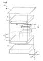
図1から図3を用いて第1実施形態の半導体レーザ光源モジュール100の構造について説明する。半導体レーザ光源モジュール100を以下、単にモジュール100とも呼ぶ。
A. First Embodiment:
The structure of the semiconductor laserlight source module 100 of the first embodiment will be described with reference to FIGS. 1 to 3. Hereinafter, the semiconductor laserlight source module 100 is also simply referred to as amodule 100.

図1および図2に示すように、第1実施形態のモジュール100は、非導電性材料からなる矩形状の筐体90内部にレーザダイオード60を備える。モジュール100は、LiDAR(Light Detection and Ranging)といった光学的測距装置に搭載される半導体レーザ装置の回路基板上に実装され、測距用のレーザ光を出射するレーザ光源として用いられる。モジュール100は、LiDAR以外の光測距装置や、ディスクの記録や読み込み、レーザプリンタ、光通信、照明装置、レーザ顕微鏡、レーザマーカ等の種々の用途のレーザ光源として用いてよい。 As shown in FIGS. 1 and 2, themodule 100 of the first embodiment includes alaser diode 60 inside arectangular housing 90 made of a non-conductive material. Themodule 100 is mounted on a circuit board of a semiconductor laser device mounted on an optical range-finding device such as LiDAR (Light Detection and Ranging), and is used as a laser light source that emits a laser beam for range-finding. Themodule 100 may be used as an optical ranging device other than LiDAR, or as a laser light source for various purposes such as recording and reading of a disk, a laser printer, optical communication, a lighting device, a laser microscope, and a laser marker.

レーザダイオード60は、出射方向DLに測距用のレーザ光を出射する端面出射型のレーザダイオードである。レーザダイオード60から出射されるレーザ光のパルス幅は、例えば5nsec程度であり、5nsecの短パルスを用いることで、測距の分解能を高めている。図1および図2には、技術の理解を容易にするため、XYZ方向とともに、モジュール100から出射されるレーザ光の出射方向DLを模式的に示した。出射方向DLは、+X方向と同一である。図示したXYZ方向および出射方向DLは、各図において共通し、向きを特定する場合には、正の方向を「+」、負の方向を「−」として、方向表記に正負の符合を併用する。 Thelaser diode 60 is an end face emission type laser diode that emits a laser beam for distance measurement in the emission direction DL. The pulse width of the laser beam emitted from thelaser diode 60 is, for example, about 5 nsec, and the resolution of distance measurement is improved by using a short pulse of 5 nsec. In order to facilitate the understanding of the technique, FIGS. 1 and 2 schematically show the emission direction DL of the laser beam emitted from themodule 100 together with the XYZ direction. The emission direction DL is the same as the + X direction. The illustrated XYZ direction and emission direction DL are common in each figure, and when specifying the direction, the positive direction is set to "+" and the negative direction is set to "-", and positive and negative signs are used together in the direction notation. ..

筐体90は、4つの平板状の側壁部90Wで構成され、側壁部90Wでレーザダイオード60を囲む。筐体90の+Z方向側(以下、上面側とも呼ぶ)は、平板状の蓋体である金属製のリッド80によって封止される。リッド80は、非導電性材料で構成されてもよい。レーザダイオード60に対して+X方向側の側壁部90Wには、出射方向DLと重なる位置に透光部92を備え、レーザダイオード60から出射されるレーザ光を透過する。 Thehousing 90 is composed of four flatside wall portions 90W, and theside wall portion 90W surrounds thelaser diode 60. The + Z direction side (hereinafter, also referred to as the upper surface side) of thehousing 90 is sealed by ametal lid 80 which is a flat plate-shaped lid. Thelid 80 may be made of a non-conductive material. Theside wall portion 90W on the + X direction side of thelaser diode 60 is provided with alight transmitting portion 92 at a position overlapping the emission direction DL, and transmits the laser light emitted from thelaser diode 60.

図2および図3を用いて、モジュール100の内部構造の詳細について説明する。図2に示すように、モジュール100は、Z方向に沿って下面側から順に、セラミック製の基台部30と、第二導電体40と、レーザダイオード60と、第一導電体70とを筐体90内部に備える。なお、図2では、技術の理解を容易にするため筐体90の図示を省略している。 The details of the internal structure of themodule 100 will be described with reference to FIGS. 2 and 3. As shown in FIG. 2, themodule 100 encapsulates aceramic base portion 30, asecond conductor 40, alaser diode 60, and afirst conductor 70 in this order from the lower surface side along the Z direction. Prepared inside thebody 90. In FIG. 2, thehousing 90 is not shown in order to facilitate understanding of the technology.

本実施形態において、基台部30には、窒化アルミニウムからなるセラミック基板が用いられるが、アルミナなどの種々のセラミック材料が用いられてもよい。第二導電体40は、金属層48と、導電体からなるサブマウントSmとの互いの面を当接して構成される。サブマウントSmは省略されてもよい。図3に示すように、基台部30と、第二導電体40と、レーザダイオード60と、第一導電体70とは互いに当接された状態でZ方向に沿って配置されている。本明細書において、「当接する」とは、各部材同士が直接接触している状態のほか、各部材間にハンダ接合や銀ペーストなどの接着剤、ろう材層を介在させる状態をも含む。 In the present embodiment, a ceramic substrate made of aluminum nitride is used for thebase portion 30, but various ceramic materials such as alumina may be used. Thesecond conductor 40 is formed by abutting the surfaces of themetal layer 48 and the submount Sm made of the conductor on each other. Submount Sm may be omitted. As shown in FIG. 3, thebase portion 30, thesecond conductor 40, thelaser diode 60, and thefirst conductor 70 are arranged along the Z direction in a state of being in contact with each other. In the present specification, "contacting" includes not only a state in which the members are in direct contact with each other, but also a state in which an adhesive such as a solder joint or a silver paste or a brazing material layer is interposed between the members.

レーザダイオード60は、図3に示すように、レーザ光を発生させるpn接合からなる発光層を内部に有する半導体層63を備える。半導体層63は、例えば、n型クラッド層とp型クラッド層とで活性層を挟持したダブルへテロ構造の層をn型基板上に備えて構成される。レーザダイオード60のX方向の両端面は、劈開面として形成され、素子内部に共振器を構成するレーザ出射側端面およびレーザ反射側端面として機能する。レーザ出射側端面に低反射率コーティング膜を備え、レーザ反射側端面に高反射率コーティング膜を備えてもよい。半導体層63は、+Z方向側で正極として機能する平板状の第一電極64と、−Z方向側で負極として機能する平板状の第二電極62とによって挟み込まれて構成される。第一電極64から第二電極62に、すなわちpn接合の順方向に電流を流すことにより、n型クラッド層からの電子と、p型クラッド層からの正孔とが活性層に流入して結合することで発光する。活性層内の光は、誘導放出により出射方向DLにレーザ光として出射される。 As shown in FIG. 3, thelaser diode 60 includes asemiconductor layer 63 having a light emitting layer formed of a pn junction that generates laser light inside. Thesemiconductor layer 63 is configured to include, for example, a layer having a double hetero structure in which an active layer is sandwiched between an n-type clad layer and a p-type clad layer on an n-type substrate. Both end faces of thelaser diode 60 in the X direction are formed as cleavage planes, and function as laser emission side end faces and laser reflection side end faces forming a resonator inside the element. A low reflectance coating film may be provided on the end face on the laser emitting side, and a high reflectance coating film may be provided on the end face on the laser reflecting side. Thesemiconductor layer 63 is configured by being sandwiched between a flat plate-shapedfirst electrode 64 that functions as a positive electrode on the + Z direction side and a flat plate-shapedsecond electrode 62 that functions as a negative electrode on the −Z direction side. By passing a current from thefirst electrode 64 to thesecond electrode 62, that is, in the forward direction of the pn junction, electrons from the n-type clad layer and holes from the p-type clad layer flow into the active layer and are bonded. It emits light by doing. The light in the active layer is emitted as laser light in the emission direction DL by stimulated emission.

第一電極64は、上面側で第一導電体70と当接し、互いに電気的に接続される。第一導電体70は、平板状の金属層である。本実施形態において、モジュール100は、図3および図1に示すように、筐体90の外部側、すなわち+Y方向側の側壁部90Wの外表面に端面70Wを露出した状態で備える。端面70Wは、第一導電体70の+Y方向側の端面である。側壁部90Wから露出した第一導電体70の端面70Wは、半導体レーザ装置の回路基板上の正極側(アノード)の導体配線と、モジュール100とを電気的に接続させるための第一接続部として機能する。本実施形態において、端面70Wには、金錫ハンダで構成される第一実装部72が備えられる。モジュール100は、第一実装部72のはんだ付けにより半導体レーザ装置の回路基板の表面に実装される。 Thefirst electrode 64 comes into contact with thefirst conductor 70 on the upper surface side and is electrically connected to each other. Thefirst conductor 70 is a flat metal layer. In the present embodiment, as shown in FIGS. 3 and 1, themodule 100 is provided with theend face 70W exposed on the outer surface of theside wall portion 90W on the outer side of thehousing 90, that is, on the + Y direction side. The end face 70W is the end face of thefirst conductor 70 on the + Y direction side. Theend surface 70W of thefirst conductor 70 exposed from theside wall portion 90W serves as a first connection portion for electrically connecting the conductor wiring on the positive electrode side (anode) on the circuit board of the semiconductor laser device and themodule 100. Function. In the present embodiment, theend face 70W is provided with a first mountingportion 72 made of gold-tin solder. Themodule 100 is mounted on the surface of the circuit board of the semiconductor laser device by soldering the first mountingportion 72.

第二電極62は、下面側で第二導電体40と当接し、互いに電気的に接続される。第二導電体40は、上述したように、平板状の金属層48と、導電性のサブマウントSmとで構成される。本実施形態では、第二電極62は、サブマウントSmの上面側と当接される。モジュール100は、図3および図1に示すように、筐体90の外部側、すなわち+Y方向側の側壁部90Wの外表面に端面40Wを露出した状態で備える。端面40Wは、第二導電体40(本実施形態において、金属層48)の+Y方向側の端面である。側壁部90Wから露出した第二導電体40の端面40Wは、半導体レーザ装置の回路基板上の負極側(カソード)の導体配線と、モジュール100とを電気的に接続させるための第二接続部として機能する。本実施形態において、端面40Wには、金錫ハンダで構成される第二実装部42が備えられる。モジュール100は、第二実装部42のはんだ付けにより半導体レーザ装置の回路基板上に表面実装される。 Thesecond electrode 62 comes into contact with thesecond conductor 40 on the lower surface side and is electrically connected to each other. As described above, thesecond conductor 40 is composed of aflat metal layer 48 and a conductive submount Sm. In the present embodiment, thesecond electrode 62 is in contact with the upper surface side of the submount Sm. As shown in FIGS. 3 and 1, themodule 100 is provided with anend face 40W exposed on the outer surface of theside wall portion 90W on the outer side of thehousing 90, that is, on the + Y direction side. The end face 40W is the end face on the + Y direction side of the second conductor 40 (themetal layer 48 in this embodiment). Theend face 40W of thesecond conductor 40 exposed from theside wall portion 90W serves as a second connecting portion for electrically connecting the conductor wiring on the negative electrode side (cathode) on the circuit board of the semiconductor laser device and themodule 100. Function. In the present embodiment, theend face 40W is provided with a second mountingportion 42 made of gold-tin solder. Themodule 100 is surface-mounted on the circuit board of the semiconductor laser device by soldering the second mountingportion 42.

モジュール100は、上述したように第一実装部72と第二実装部42とを介して半導体レーザ装置の回路基板上に実装され、レーザダイオードドライバ(以下、LDドライバとも呼ぶ)と電気的に接続される。LDドライバは、半導体レーザ装置の制御装置から出力される発光信号に従ってレーザダイオード60を駆動し、レーザ光の出力のON/OFFを実行する。発光信号とは、レーザダイオード60の発光タイミングを指示する電気信号である。レーザダイオード60には、第一導電体70から第一電極64を介して、LDドライバから電源および信号が供給される。 As described above, themodule 100 is mounted on the circuit board of the semiconductor laser device via the first mountingportion 72 and the second mountingportion 42, and is electrically connected to the laser diode driver (hereinafter, also referred to as LD driver). Will be done. The LD driver drives thelaser diode 60 according to the light emission signal output from the control device of the semiconductor laser device, and turns on / off the output of the laser beam. The light emitting signal is an electric signal that indicates the light emitting timing of thelaser diode 60. A power source and a signal are supplied from the LD driver to thelaser diode 60 from thefirst conductor 70 via thefirst electrode 64.

以上説明したように、本実施形態の半導体レーザ光源モジュール100によれば、正極側となる第一導電体70と、レーザダイオード60の第一電極64とが当接されて電気的に接続されるとともに、負極側となる第二導電体40と、第二電極62とが当接されて電気的に接続される。モジュール100は、側壁部90Wの外部側に第一接続部と、第二接続部とを備え、半導体レーザ装置の回路基板上に実装可能に構成される。したがって、本実施形態のモジュール100によれば、ボンディングワイヤを用いることなくレーザダイオード60に電流を供給でき、寄生インダクタンスの発生を抑制することができる。 As described above, according to the semiconductor laserlight source module 100 of the present embodiment, thefirst conductor 70 on the positive electrode side and thefirst electrode 64 of thelaser diode 60 are brought into contact with each other and electrically connected. At the same time, thesecond conductor 40 on the negative electrode side and thesecond electrode 62 are brought into contact with each other and electrically connected. Themodule 100 includes a first connection portion and a second connection portion on the outer side of theside wall portion 90W, and is configured to be mountable on a circuit board of a semiconductor laser device. Therefore, according to themodule 100 of the present embodiment, the current can be supplied to thelaser diode 60 without using the bonding wire, and the generation of parasitic inductance can be suppressed.

本実施形態のモジュール100によれば、平板状の金属層からなる第一導電体70の+Y方向側の端面70Wを+Y方向側の側壁部90Wの外表面に露出させることにより、半導体レーザ装置の回路基板上に実装するための第一接続部が構成される。したがって、第一導電体70によりレーザダイオード60の第一電極64側からの放熱性を向上させることができる。第一電極64と第一接続部とを一つの金属層である第一導電体70で電気的に接続することにより、基板間容量やインダクタンスの発生を抑制することができる。 According to themodule 100 of the present embodiment, theend face 70W on the + Y direction side of thefirst conductor 70 made of a flat metal layer is exposed to the outer surface of theside wall portion 90W on the + Y direction side, so that the semiconductor laser apparatus can be used. A first connection is configured for mounting on a circuit board. Therefore, thefirst conductor 70 can improve the heat dissipation from thefirst electrode 64 side of thelaser diode 60. By electrically connecting thefirst electrode 64 and the first connecting portion with thefirst conductor 70, which is one metal layer, it is possible to suppress the generation of capacitance between substrates and inductance.

本実施形態のモジュール100によれば、平板状の第二導電体40(より具体的には金属層48)の+Y方向側の端面40Wを+Y方向側の側壁部90Wの外表面に露出させることにより、回路基板上に実装するための第二接続部が構成される。したがって、金属層48によりレーザダイオード60の第二電極62側からの放熱性を向上させることができる。第二電極62と第二接続部とを一つの金属層48で電気的に接続することにより、基板間容量やインダクタンスの発生を抑制することができる。 According to themodule 100 of the present embodiment, theend face 40W on the + Y direction side of the flat plate-shaped second conductor 40 (more specifically, the metal layer 48) is exposed to the outer surface of theside wall portion 90W on the + Y direction side. 2. The second connection portion for mounting on the circuit board is configured. Therefore, themetal layer 48 can improve the heat dissipation from thesecond electrode 62 side of thelaser diode 60. By electrically connecting thesecond electrode 62 and the second connecting portion with onemetal layer 48, it is possible to suppress the generation of inter-board capacitance and inductance.

本実施形態のモジュール100によれば、第二導電体40と当接するセラミック製の基台部30を筐体90の下面側に備える。したがって、モジュール100の放熱性能や耐衝撃性を高めるとともに、絶縁性能や低熱膨張性を向上させることができる。 According to themodule 100 of the present embodiment, theceramic base portion 30 that comes into contact with thesecond conductor 40 is provided on the lower surface side of thehousing 90. Therefore, the heat dissipation performance and impact resistance of themodule 100 can be improved, and the insulation performance and low thermal expansion property can be improved.

B.第2実施形態:
図4に示すように、第2実施形態の半導体レーザ光源モジュール100bは、第一導電体70に代えて第一導電体70bと、第二導電体40に代えて第二導電体40bと、基台部30に代えて下面金属層20とを備え、更に、第一導体面74および第二導体面44を備える点で第1実施形態のモジュール100と相違する。下面金属層20は、平板の金属層である。下面金属層20のZ方向での厚みは、本実施形態においてリッド80と同じであるが、任意の厚みで設定してよい。
B. Second embodiment:
As shown in FIG. 4, the semiconductor laser light source module 100b of the second embodiment is based on afirst conductor 70b instead of thefirst conductor 70 and asecond conductor 40b instead of thesecond conductor 40. It is different from themodule 100 of the first embodiment in that it is provided with a lowersurface metal layer 20 instead of thebase portion 30, and is further provided with afirst conductor surface 74 and asecond conductor surface 44. The lowersurface metal layer 20 is a flat metal layer. The thickness of the lowersurface metal layer 20 in the Z direction is the same as that of thelid 80 in this embodiment, but may be set to any thickness.

本実施形態において、第一導電体70bのXY平面視での外形は、第1実施形態の第一導電体70の外形よりも小さく構成される。これにより、第一導電体70bは、筐体90の外部側に露出せず、第一電極64と当接した状態で筐体90内に収容される。第二導電体40bは、サブマウントSmと、金属層48bとを備える。金属層48bのXY平面視での外形は、第1実施形態の金属層48の外形よりも小さくなるように構成される。これにより、第二導電体40bの金属層48bは、筐体90の外部側に露出せず筐体90内に収容される。サブマウントSmやレーザダイオード60の構成は第1実施形態と同様である。 In the present embodiment, the outer shape of thefirst conductor 70b in the XY plan view is smaller than the outer shape of thefirst conductor 70 of the first embodiment. As a result, thefirst conductor 70b is not exposed to the outside of thehousing 90 and is housed in thehousing 90 in a state of being in contact with thefirst electrode 64. Thesecond conductor 40b includes a submount Sm and ametal layer 48b. The outer shape of themetal layer 48b in the XY plan view is configured to be smaller than the outer shape of themetal layer 48 of the first embodiment. As a result, themetal layer 48b of thesecond conductor 40b is housed in thehousing 90 without being exposed to the outside of thehousing 90. The configuration of the submount Sm and thelaser diode 60 is the same as that of the first embodiment.

第一導体面74および第二導体面44は、筐体90の+Y方向側の側壁部90Wの外表面上に形成される導体配線の電極パッドである。第一導体面74および第二導体面44は、既知の印刷技術やフォトリソグラフィ技術によって側壁部90Wの表面上に形成され、側壁部90Wの厚みよりも小さい厚みを有する。第一導体面74の表面上には、第一実装部72が形成され、第二導体面44の表面上には、第二実装部42が形成される。 Thefirst conductor surface 74 and thesecond conductor surface 44 are electrode pads for conductor wiring formed on the outer surface of theside wall portion 90W on the + Y direction side of thehousing 90. Thefirst conductor surface 74 and thesecond conductor surface 44 are formed on the surface of theside wall portion 90W by a known printing technique or photolithography technique, and have a thickness smaller than the thickness of theside wall portion 90W. The first mountingportion 72 is formed on the surface of thefirst conductor surface 74, and the second mountingportion 42 is formed on the surface of thesecond conductor surface 44.

第一導体面74は、金属製のリッド80と当接し、リッド80は、第一導電体70bと当接して構成される。これにより、第一導体面74は、リッド80および第一導電体70bを介して、第一電極64と電気的に接続される。他方、第二導体面44は、下面金属層20と当接し、下面金属層20は、第二導電体40bと当接して構成される。これにより、第二導体面44は、下面金属層20および第二導電体40bを介して、第二電極62と電気的に接続される。このように、本実施形態のモジュール100bでは、側壁部90Wの外部側に設けられる第一導体面74が、半導体レーザ装置の正極と第一導電体70bとを電気的に接続する第一接続部として機能し、第二導体面44が、半導体レーザ装置の負極と第二導電体40bとを電気的に接続する第二接続部として機能する。 Thefirst conductor surface 74 is in contact with themetal lid 80, and thelid 80 is in contact with thefirst conductor 70b. As a result, thefirst conductor surface 74 is electrically connected to thefirst electrode 64 via thelid 80 and thefirst conductor 70b. On the other hand, thesecond conductor surface 44 is in contact with the lowersurface metal layer 20, and the lowersurface metal layer 20 is in contact with thesecond conductor 40b. As a result, thesecond conductor surface 44 is electrically connected to thesecond electrode 62 via thelower metal layer 20 and thesecond conductor 40b. As described above, in the module 100b of the present embodiment, thefirst conductor surface 74 provided on the outer side of theside wall portion 90W electrically connects the positive electrode of the semiconductor laser device and thefirst conductor 70b. Thesecond conductor surface 44 functions as a second connecting portion that electrically connects the negative electrode of the semiconductor laser device and thesecond conductor 40b.

以上のように、第2実施形態のモジュール100bによれば、第一実装部72が、側壁部90Wの厚みよりも小さい厚みを有する第一導体面74上に形成されるので、第一実装部72周辺の熱容量を低減することができる。したがって、例えば、リフロー方式による第一実装部72のはんだ付けによりモジュール100bを回路基板上に実装する場合、第一実装部72の溶融性を向上させることができる。 As described above, according to the module 100b of the second embodiment, since the first mountingportion 72 is formed on thefirst conductor surface 74 having a thickness smaller than the thickness of theside wall portion 90W, the first mounting portion The heat capacity around 72 can be reduced. Therefore, for example, when the module 100b is mounted on the circuit board by soldering the first mountingportion 72 by the reflow method, the meltability of the first mountingportion 72 can be improved.

第2実施形態のモジュール100bによれば、第二実装部42が、側壁部90Wの厚みよりも小さい厚みを有する第二導体面44上に形成されるので、第二実装部42周辺の熱容量を低減することができる。したがって、例えば、リフロー方式による第二実装部42のはんだ付けによりモジュール100bを回路基板上に実装する場合、第二実装部42の溶融性を向上させることができる。 According to the module 100b of the second embodiment, the second mountingportion 42 is formed on thesecond conductor surface 44 having a thickness smaller than the thickness of theside wall portion 90W, so that the heat capacity around the second mountingportion 42 can be increased. It can be reduced. Therefore, for example, when the module 100b is mounted on the circuit board by soldering the second mountingportion 42 by the reflow method, the meltability of the second mountingportion 42 can be improved.

第2実施形態のモジュール100bによれば、第一実装部72は、第一導電体70bと当接せず、リッド80を介して第一導電体70bと電気的に接続される。したがって、第一実装部72周辺の熱容量を第一導電体70bと当接する状態よりも低減させ、モジュール100b実装時の第一実装部72の溶融性を向上させることができる。 According to the module 100b of the second embodiment, the first mountingportion 72 does not come into contact with thefirst conductor 70b, but is electrically connected to thefirst conductor 70b via thelid 80. Therefore, the heat capacity around the first mountingportion 72 can be reduced as compared with the state of being in contact with thefirst conductor 70b, and the meltability of the first mountingportion 72 at the time of mounting the module 100b can be improved.

第2実施形態のモジュール100bによれば、第二実装部42は、第二導電体40bと当接せず、下面金属層20を介して第二導電体40bと電気的に接続される。したがって、セラミック製の基台部30を省略しつつ、下面金属層20によりモジュール100bの下面側の放熱性を向上させることができる。また、第二実装部42周辺の熱容量を第二導電体40bと当接する状態よりも低減させ、モジュール100b実装時の第二実装部42の溶融性を向上させることができる。 According to the module 100b of the second embodiment, the second mountingportion 42 does not come into contact with thesecond conductor 40b, but is electrically connected to thesecond conductor 40b via thelower metal layer 20. Therefore, the heat dissipation of the lower surface side of the module 100b can be improved by the lowersurface metal layer 20 while omitting theceramic base portion 30. Further, the heat capacity around the second mountingportion 42 can be reduced as compared with the state of being in contact with thesecond conductor 40b, and the meltability of the second mountingportion 42 at the time of mounting the module 100b can be improved.

C.第3実施形態:
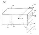
図5および図6Aに示すように、第3実施形態のモジュール100cは、第一導電体70に代えて第一導電体70bと、第二導電体40に代えて第二導電体40bと、基台部30に代えて基台部30cとを備える点で第1実施形態のモジュール100と相違する。第一導電体70bおよび第二導電体40bは、第2実施形態の第一導電体70bおよび第二導電体40bと同一であり、筐体90内に収容される。また、第3実施形態のモジュール100cは、更に、基台側金属層20cと、第一導体面74および第二導体面44と、コリメータレンズ94とを備える点で第1実施形態のモジュール100と相違する。コリメータレンズ94は、レーザダイオード60から射出されたレーザ光を収差補正して平行光にするレンズである。コリメータレンズ94は、透光部92よりも出射方向DL側に備えられる。
C. Third Embodiment:
As shown in FIGS. 5 and 6A, themodule 100c of the third embodiment is based on thefirst conductor 70b instead of thefirst conductor 70 and thesecond conductor 40b instead of thesecond conductor 40. It differs from themodule 100 of the first embodiment in that it includes abase portion 30c instead of thebase portion 30. Thefirst conductor 70b and thesecond conductor 40b are the same as thefirst conductor 70b and thesecond conductor 40b of the second embodiment, and are housed in thehousing 90. Further, themodule 100c of the third embodiment is different from themodule 100 of the first embodiment in that it further includes a base-side metal layer 20c, afirst conductor surface 74 and asecond conductor surface 44, and acollimator lens 94. It's different. Thecollimator lens 94 is a lens that corrects aberrations of the laser light emitted from thelaser diode 60 to make it parallel light. Thecollimator lens 94 is provided on the DL side in the emission direction with respect to thelight transmitting portion 92.

本実施形態では、第一導体面74と第二導体面44とが、側壁部90Wのうち出射方向DLとは逆側である−X方向側の側壁部90Wに備えられる。第一実装部72および第二実装部42は、第2実施形態と同様に、第一導体面74と第二導体面44との表面上にそれぞれ備えられる。本実施形態において、第一導体面74は、第2実施形態と同様に、金属製のリッド80と当接し、第一導電体70bを介して第一電極64と電気的に接続される。 In the present embodiment, thefirst conductor surface 74 and thesecond conductor surface 44 are provided on theside wall portion 90W on the −X direction side of theside wall portion 90W, which is opposite to the emission direction DL. The first mountingportion 72 and the second mountingportion 42 are provided on the surfaces of thefirst conductor surface 74 and thesecond conductor surface 44, respectively, as in the second embodiment. In the present embodiment, thefirst conductor surface 74 is in contact with themetal lid 80 and is electrically connected to thefirst electrode 64 via thefirst conductor 70b, as in the second embodiment.

セラミック製の基台部30cは、図6Aに示すように、円柱状の貫通孔に電気めっき等により導体が充填されているいわゆるスルーホールビアとも呼ばれるビア状接続部32を複数備える。ビア状接続部32は、上面側で第二導電体40bの金属層48bと当接されるとともに、下面側で基台側金属層20cと当接される。 As shown in FIG. 6A, theceramic base portion 30c includes a plurality of via-shaped connectingportions 32, which are also called through-hole vias, in which a columnar through hole is filled with a conductor by electroplating or the like. The via-shaped connectingportion 32 is in contact with themetal layer 48b of thesecond conductor 40b on the upper surface side and is in contact with themetal layer 20c on the base side on the lower surface side.

基台側金属層20cは、基台部30cのうち第二導電体40bと当接する側とは逆側、すなわち基台部30cの下面側に備えられる。基台側金属層20cは、モジュール100cの下面全域に亘って備えられ、更に、モジュール100cの−X方向側の側壁部90Wの外表面に至る。−X方向側の側壁部90Wの外表面に備えられる基台側金属層20cを金属層20Wとしたとき、金属層20Wは、第二導体面44と当接して互いに電気的に接続される。金属層20Wは、基台側金属層20cに接続される導体配線で構成されてもよい。第二導体面44は、基台側金属層20cと第二導電体40bとを介して第二電極62と電気的に接続される。このように、本実施形態のモジュール100cでは、第一導体面74が−X方向側の側壁部90Wで第一接続部として機能し、第二導体面44が−X方向側の側壁部90Wで第二接続部として機能する。 The baseside metal layer 20c is provided on the side of thebase portion 30c opposite to the side that comes into contact with thesecond conductor 40b, that is, on the lower surface side of thebase portion 30c. The base-side metal layer 20c is provided over the entire lower surface of themodule 100c, and further reaches the outer surface of theside wall portion 90W on the −X direction side of themodule 100c. When the base-side metal layer 20c provided on the outer surface of theside wall portion 90W on the −X direction side is themetal layer 20W, themetal layer 20W comes into contact with thesecond conductor surface 44 and is electrically connected to each other. Themetal layer 20W may be composed of conductor wiring connected to the base-side metal layer 20c. Thesecond conductor surface 44 is electrically connected to thesecond electrode 62 via the base-side metal layer 20c and thesecond conductor 40b. As described above, in themodule 100c of the present embodiment, thefirst conductor surface 74 functions as the first connecting portion at theside wall portion 90W on the −X direction side, and thesecond conductor surface 44 at theside wall portion 90W on the −X direction side. Functions as a second connection.

次に、図6B、図6Cを用いて、モジュール100cを備える半導体レーザ装置400cの構成について説明する。図6Bには、半導体レーザ装置400cに備えられる回路基板PBの+X方向側の表面が模式的に示されている。回路基板PBは、導体の配線が形成されたプリント配線板である。モジュール100cは、回路基板PBの+X方向側の表面に実装される。回路基板PBには、モジュール100cのほか、キャパシタやLDドライバ、プリドライバ、コネクタ等の図示しない電子部品が実装される。 Next, the configuration of thesemiconductor laser device 400c including themodule 100c will be described with reference to FIGS. 6B and 6C. FIG. 6B schematically shows the surface of the circuit board PB provided in thesemiconductor laser device 400c on the + X direction side. The circuit board PB is a printed wiring board on which conductor wiring is formed. Themodule 100c is mounted on the surface of the circuit board PB on the + X direction side. In addition to themodule 100c, electronic components (not shown) such as capacitors, LD drivers, predrivers, and connectors are mounted on the circuit board PB.

図6Bに示すように、本実施形態の半導体レーザ装置400cは、回路基板PB上に、複数のモジュール100cを備える。モジュール100cは、図6Bの例において9つ備えられる。上述したように、本実施形態のモジュール100cでは、第一導体面74と第二導体面44とが、出射方向DLとは逆側である−X方向側の側壁部90Wに備えられる。図6Cに示すように、各モジュール100cは、第一実装部72と第二実装部42との一般的なリフロー工程によるはんだ付けによって回路基板PB上に実装される。これにより、第一接続部として機能する第一導体面74と、第二接続部として機能する第二導体面44とが、回路基板PB上の導体配線に当接された状態で回路基板PBの表面に実装される。実装された各モジュール100cのレーザ光の出射方向DLは、+X方向側にそれぞれ揃えられる。 As shown in FIG. 6B, thesemiconductor laser device 400c of the present embodiment includes a plurality ofmodules 100c on the circuit board PB. Ninemodules 100c are provided in the example of FIG. 6B. As described above, in themodule 100c of the present embodiment, thefirst conductor surface 74 and thesecond conductor surface 44 are provided on theside wall portion 90W on the −X direction side opposite to the emission direction DL. As shown in FIG. 6C, eachmodule 100c is mounted on the circuit board PB by soldering the first mountingportion 72 and the second mountingportion 42 by a general reflow process. As a result, thefirst conductor surface 74 that functions as the first connection portion and thesecond conductor surface 44 that functions as the second connection portion of the circuit board PB are in contact with the conductor wiring on the circuit board PB. It is mounted on the surface. The emission direction DL of the laser beam of each of the mountedmodules 100c is aligned on the + X direction side.

図6Bおよび図6Cに示すように、各モジュール100cは、回路基板PBの表面にZ方向とY方向とのそれぞれにおいて互いに等間隔となるように規則的に配列され、いわゆる二次元アレイを構成している。 As shown in FIGS. 6B and 6C, eachmodule 100c is regularly arranged on the surface of the circuit board PB so as to be evenly spaced from each other in the Z direction and the Y direction, respectively, forming a so-called two-dimensional array. ing.

図6Cに示すように、本実施形態の半導体レーザ装置400cは、各モジュール100cの出射方向DL側に、更にマイクロレンズアレイ300を備える。マイクロレンズアレイ300は、複数の集光レンズを配列した板状の透光部材である。マイクロレンズアレイ300の各集光レンズは、各モジュール100cから出射されるレーザ光の光路のそれぞれに対応する位置に配置される。 As shown in FIG. 6C, thesemiconductor laser device 400c of the present embodiment further includes amicrolens array 300 on the emission direction DL side of eachmodule 100c. Themicrolens array 300 is a plate-shaped translucent member in which a plurality of condensing lenses are arranged. Each condensing lens of themicrolens array 300 is arranged at a position corresponding to each of the optical paths of the laser light emitted from eachmodule 100c.

第3実施形態のモジュール100cによれば、複数のビア状接続部32を備えるセラミック製の基台部30cと、基台部30cの下面側の基台側金属層20cとを備える。したがって、基台部30cと基台側金属層20cとによってモジュール100cの下面側の放熱性能や耐衝撃性を高めることができる。また、第二実装部42は、第二導体面44上に備えられるので、金属層48b上に第二実装部42を備える場合よりも第二実装部42周辺の熱容量を低減することができる。 According to themodule 100c of the third embodiment, aceramic base portion 30c having a plurality of via-shaped connectingportions 32 and a baseside metal layer 20c on the lower surface side of thebase portion 30c are provided. Therefore, the heat dissipation performance and impact resistance of the lower surface side of themodule 100c can be improved by thebase portion 30c and the baseside metal layer 20c. Further, since the second mountingportion 42 is provided on thesecond conductor surface 44, the heat capacity around the second mountingportion 42 can be reduced as compared with the case where the second mountingportion 42 is provided on themetal layer 48b.

本実施形態のモジュール100cによれば、第一導体面74が−X方向側の側壁部90Wで第一接続部として機能し、第二導体面44が−X方向側の側壁部90Wで第二接続部として機能する。すなわち、第一接続部と第二接続部とが、レーザダイオード60の位置に対して出射方向DLとは逆側の側壁部90Wの外部側に備えられる。したがって、端面出射型のレーザダイオード60を、例えば、出射方向DLを半導体レーザ装置の回路基板の面方向に対して垂直な方向に一致させた状態で回路基板上に実装することができる。本実施形態のモジュール100cを複数備えることにより、回路基板上にアレイ状のレーザ光源を配置することができる。 According to themodule 100c of the present embodiment, thefirst conductor surface 74 functions as the first connection portion at theside wall portion 90W on the −X direction side, and thesecond conductor surface 44 is the secondside wall portion 90W on the −X direction side. Functions as a connection. That is, the first connection portion and the second connection portion are provided on the outer side of theside wall portion 90W on the side opposite to the emission direction DL with respect to the position of thelaser diode 60. Therefore, the end face emissiontype laser diode 60 can be mounted on the circuit board in a state where, for example, the emission direction DL is aligned with the direction perpendicular to the surface direction of the circuit board of the semiconductor laser apparatus. By providing a plurality ofmodules 100c of the present embodiment, an array of laser light sources can be arranged on the circuit board.

本実施形態のモジュール100cによれば、レーザダイオード60の出射方向DL側にコリメータレンズ94を備えるので、モジュール100cを平行光のレーザ光を出射するレーザ光源とすることができる。 According to themodule 100c of the present embodiment, since thecollimator lens 94 is provided on the DL side of thelaser diode 60 in the emission direction, themodule 100c can be used as a laser light source for emitting a laser beam of parallel light.

本実施形態の半導体レーザ装置400cによれば、複数の半導体レーザ光源モジュール100cのそれぞれは、レーザ光の出射方向DL側とは逆側となる第一接続部と第二接続部とが回路基板PBの導体配線に当接された状態で回路基板PBの表面に規則的な配列で実装される。したがって、回路基板PBの面方向に垂直な方向に複数のレーザ光を照射するレーザアレイを備えることができ、半導体レーザ装置400cを高出力化することができる。 According to thesemiconductor laser apparatus 400c of the present embodiment, in each of the plurality of semiconductor laserlight source modules 100c, the first connection portion and the second connection portion on the opposite side to the DL side in the emission direction of the laser light are circuit boards PB. It is mounted in a regular arrangement on the surface of the circuit board PB in a state of being in contact with the conductor wiring of. Therefore, it is possible to provide a laser array that irradiates a plurality of laser beams in a direction perpendicular to the plane direction of the circuit board PB, and it is possible to increase the output of thesemiconductor laser device 400c.

本実施形態の半導体レーザ装置400cによれば、複数のモジュール100cから出射されるそれぞれのレーザ光の光路に対応するマイクロレンズアレイ300を備える。したがって、複数のモジュール100cのそれぞれから出射されるレーザ光を任意の光路に設定することができる。 According to thesemiconductor laser apparatus 400c of the present embodiment, themicrolens array 300 corresponding to the optical path of each laser beam emitted from the plurality ofmodules 100c is provided. Therefore, the laser light emitted from each of the plurality ofmodules 100c can be set to an arbitrary optical path.

D.第4実施形態:
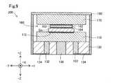
図7から図9を用いて第4実施形態の半導体レーザ光源モジュール200の構造について説明する。半導体レーザ光源モジュール200を以下、単にモジュール200とも呼ぶ。図7および図8に示すように、第4実施形態のモジュール200は、矩形状の非導電性材料からなる筐体190内部にレーザダイオード160を備えて構成される。図8に示すように、モジュール200は、Z方向に沿って下面側から順に、セラミック製の基台部130と、キャパシタ120およびLDドライバ110と、導電体からなるサブマウントSmと、レーザダイオード160と、第三導電体170とを筐体190内部に備える。なお、図8では、技術の理解を容易にするため筐体190の図示を省略している。
D. Fourth Embodiment:
The structure of the semiconductor laserlight source module 200 of the fourth embodiment will be described with reference to FIGS. 7 to 9. Hereinafter, the semiconductor laserlight source module 200 is also simply referred to as amodule 200. As shown in FIGS. 7 and 8, themodule 200 of the fourth embodiment is configured to include alaser diode 160 inside ahousing 190 made of a rectangular non-conductive material. As shown in FIG. 8, themodule 200 includes aceramic base portion 130, acapacitor 120, anLD driver 110, a submount Sm made of a conductor, and alaser diode 160 in this order from the lower surface side along the Z direction. And thethird conductor 170 are provided inside thehousing 190. Note that in FIG. 8, thehousing 190 is not shown in order to facilitate understanding of the technology.

レーザダイオード160は、レーザ光を発生させるpn接合からなる発光層を内部に有する半導体層163を備える。半導体層163は、−Z方向側で正極として機能する第一電極164と、Z方向側で負極として機能する第二電極162とによって挟み込まれた状態で形成される。レーザダイオード160の構成は第1実施形態でのレーザダイオード60と同様であるが、第一電極164と、第二電極162との位置関係がZ方向において逆になる点で、第1実施形態とは相違する。すなわち、本実施形態のモジュール200では、レーザダイオード160よりも+Z方向側が負極側であり、−Z方向側が正極側である。 Thelaser diode 160 includes asemiconductor layer 163 having a light emitting layer formed of a pn junction that generates laser light inside. Thesemiconductor layer 163 is formed in a state of being sandwiched between afirst electrode 164 that functions as a positive electrode on the −Z direction side and asecond electrode 162 that functions as a negative electrode on the Z direction side. The configuration of thelaser diode 160 is the same as that of thelaser diode 60 in the first embodiment, but the positional relationship between thefirst electrode 164 and thesecond electrode 162 is opposite in the Z direction. Is different. That is, in themodule 200 of the present embodiment, the + Z direction side is the negative electrode side and the −Z direction side is the positive electrode side with respect to thelaser diode 160.

筐体190は、図7に示すように、レーザダイオード160を囲む側壁部190Wを備える。筐体190の上面側は、金属製のリッド180によって封止される。図7に示すように、+Y方向側の側壁部190Wには、第一配線電極195が備えられる。第一配線電極195は、一端側をリッド180の一部と当接される導体配線である。第一配線電極195の他端側は、モジュール200の下面側に設けられる第二電極パッド136と互いに電気的に接続される。+X方向側の側壁部190Wには、レーザ光の出射経路となる位置に透光部192を備え、レーザダイオード160から出射されるレーザ光を透過する。 As shown in FIG. 7, thehousing 190 includes aside wall portion 190W that surrounds thelaser diode 160. The upper surface side of thehousing 190 is sealed by ametal lid 180. As shown in FIG. 7, theside wall portion 190W on the + Y direction side is provided with thefirst wiring electrode 195. Thefirst wiring electrode 195 is a conductor wiring whose one end side is in contact with a part of thelid 180. The other end side of thefirst wiring electrode 195 is electrically connected to thesecond electrode pad 136 provided on the lower surface side of themodule 200. Theside wall portion 190W on the + X direction side is provided with alight transmitting portion 192 at a position serving as an emission path of the laser light, and transmits the laser light emitted from thelaser diode 160.

LDドライバ110は、図9に示すように、基台部130の上面側に当接された状態で配置される。LDドライバ110は、図8および図9に示すように、上面にドライバ電極112を備える。ドライバ電極112は、サブマウントSmと当接されて互いに電気的に接続される導体配線である。サブマウントSmが省略される場合には、ドライバ電極112は、レーザダイオード160の第二電極162と当接されて電気的に接続される。LDドライバ110は、半導体レーザ装置の制御装置から出力される発光信号に従ってレーザダイオード160を駆動し、ドライバ電極112を介して第一電極164にレーザダイオード160の電源および信号を供給してレーザ光の出力のON/OFFを実行する。 As shown in FIG. 9, theLD driver 110 is arranged in contact with the upper surface side of thebase portion 130. As shown in FIGS. 8 and 9, theLD driver 110 includes adriver electrode 112 on the upper surface. Thedriver electrode 112 is a conductor wiring that comes into contact with the submount Sm and is electrically connected to each other. When the submount Sm is omitted, thedriver electrode 112 is in contact with thesecond electrode 162 of thelaser diode 160 and is electrically connected. TheLD driver 110 drives thelaser diode 160 according to the light emission signal output from the control device of the semiconductor laser device, and supplies the power supply and the signal of thelaser diode 160 to thefirst electrode 164 via thedriver electrode 112 to generate the laser light. Executes output ON / OFF.

第二電極162は、上面側で第三導電体170と当接されて互いに電気的に接続される。第三導電体170は、平板状の金属層であり、レーザダイオード160を挟んでLDドライバ110の一方の面側と対向するように配される。第三導電体170は、上面側をリッド180と当接されて互いに電気的に接続される。上述したように、リッド180の一部は、第一配線電極195と当接され、第二電極パッド136と電気的に接続される。第二電極パッド136は、モジュール200の下面側で半導体レーザ装置の回路基板上の負極側(カソード)の導体配線とモジュール200とを電気的に接続するための第二接続部として機能する。 Thesecond electrode 162 is in contact with thethird conductor 170 on the upper surface side and is electrically connected to each other. Thethird conductor 170 is a flat metal layer, and is arranged so as to face one surface side of theLD driver 110 with thelaser diode 160 interposed therebetween. The upper surface side of thethird conductor 170 is in contact with thelid 180 and is electrically connected to each other. As described above, a part of thelid 180 is in contact with thefirst wiring electrode 195 and is electrically connected to thesecond electrode pad 136. Thesecond electrode pad 136 functions as a second connection portion for electrically connecting the conductor wiring on the negative electrode side (cathode) on the circuit board of the semiconductor laser device and themodule 200 on the lower surface side of themodule 200.

キャパシタ120は、図8に示すように、基台部130の上面側でLDドライバ110と並列させた状態で配置される。キャパシタ120は、保持した電荷を短パルスの電流としてLDドライバ110に入力する。キャパシタ120は、基台部130に設けられる第二ビア状接続部133と当接されて互いに電気的に接続される。第二ビア状接続部133は、いわゆるスルーホールビアであり、基台部130の下面側に位置する第三電極パッド135に当接されて電気的に接続される。 As shown in FIG. 8, thecapacitor 120 is arranged in parallel with theLD driver 110 on the upper surface side of thebase portion 130. Thecapacitor 120 inputs the retained charge as a short pulse current to theLD driver 110. Thecapacitor 120 is in contact with the second via-shaped connectingportion 133 provided on thebase portion 130 and is electrically connected to each other. The second via-shaped connectingportion 133 is a so-called through-hole via, and is brought into contact with thethird electrode pad 135 located on the lower surface side of thebase portion 130 and electrically connected.

基台部130は、いわゆるセラミック基板であり、本実施形態において窒化アルミニウムが用いられるが、アルミナなどの種々のセラミック材料が用いられてもよい。基台部130は、図8に示すように、複数の第一ビア状接続部132と、第二ビア状接続部133と、第二電極パッド136と、第一電極パッド134と、第三電極パッド135と、ビア状放熱部138とを備える。 Thebase portion 130 is a so-called ceramic substrate, and aluminum nitride is used in this embodiment, but various ceramic materials such as alumina may be used. As shown in FIG. 8, thebase portion 130 includes a plurality of first via-shaped connectingportions 132, a second via-shaped connectingportion 133, asecond electrode pad 136, afirst electrode pad 134, and a third electrode. Apad 135 and a via-shapedheat radiating portion 138 are provided.

第一ビア状接続部132は、上面側をLDドライバ110の下面側の導体配線や電極パッドと電気的に接続され、下面側を第一電極パッド134と電気的に接続される。半導体レーザ装置から出力される指令信号は、第一電極パッド134から入力され、第一ビア状接続部132を介してLDドライバ110に入力される。すなわち、第一電極パッド134は、モジュール200の下面側で半導体レーザ装置の回路基板上の正極側(アノード)の導体配線とモジュール200とを電気的に接続するための第一接続部として機能する。 The upper surface side of the first via-shaped connectingportion 132 is electrically connected to the conductor wiring and the electrode pad on the lower surface side of theLD driver 110, and the lower surface side is electrically connected to thefirst electrode pad 134. The command signal output from the semiconductor laser device is input from thefirst electrode pad 134, and is input to theLD driver 110 via the first via-shaped connectingportion 132. That is, thefirst electrode pad 134 functions as a first connection portion for electrically connecting the conductor wiring on the positive electrode side (anode) on the circuit board of the semiconductor laser device and themodule 200 on the lower surface side of themodule 200. ..

ビア状放熱部138は、略直方体形状の貫通孔に電気めっき等により導体を充填されているいわゆるスルーホールビアである。ビア状放熱部138は、LDドライバ110の下面側の少なくとも一部と当接されるように配置される。本実施形態において、ビア状放熱部138は2つ備えられる。ビア状放熱部138は一つであってもよく、省略されてもよい。ビア状放熱部138は、第一ビア状接続部132や第二ビア状接続部133よりも体積が大きくなるように構成され、LDドライバ110の熱を下面側から放熱させる。本実施形態において、ビア状放熱部138は、LDドライバ110とは電気的に接続されず導体配線として機能しないが、LDドライバ110と電気的に接続されて導体配線として機能させてもよい。 The via-shapedheat radiating portion 138 is a so-called through-hole via in which a substantially rectangular parallelepiped through hole is filled with a conductor by electroplating or the like. The via-shapedheat radiating portion 138 is arranged so as to be in contact with at least a part of the lower surface side of theLD driver 110. In this embodiment, two via-shapedheat radiating portions 138 are provided. The via-shapedheat radiating portion 138 may be one or may be omitted. The via-shapedheat radiating portion 138 is configured to have a larger volume than the first via-shaped connectingportion 132 and the second via-shaped connectingportion 133, and dissipates heat from theLD driver 110 from the lower surface side. In the present embodiment, the via-shapedheat radiating unit 138 is not electrically connected to theLD driver 110 and does not function as a conductor wiring, but may be electrically connected to theLD driver 110 and function as a conductor wiring.

以上説明したように、本実施形態の半導体レーザ光源モジュール200によれば、筐体190内に収容されたLDドライバ110と、レーザダイオード160の第一電極164とが当接されて電気的に接続されるとともに、第三導電体170と、第二電極162とが当接されて電気的に接続される。モジュール200は、第二電極162と電気的に接続される第二電極パッド136と、第二電極162に電気的に接続される第一電極パッド134とを側壁部190Wの外部側に備えることにより、半導体レーザ装置の回路基板上に実装可能に構成される。したがって、ボンディングワイヤを用いることなく筐体190内のLDドライバ110からレーザダイオード160に電流を供給でき、寄生インダクタンスの発生を抑制することができる。 As described above, according to the semiconductor laserlight source module 200 of the present embodiment, theLD driver 110 housed in thehousing 190 and thefirst electrode 164 of thelaser diode 160 are brought into contact with each other and electrically connected. At the same time, thethird conductor 170 and thesecond electrode 162 are brought into contact with each other and electrically connected. Themodule 200 is provided with asecond electrode pad 136 electrically connected to thesecond electrode 162 and afirst electrode pad 134 electrically connected to thesecond electrode 162 on the outer side of theside wall portion 190W. , It is configured to be mountable on the circuit board of a semiconductor laser device. Therefore, the current can be supplied from theLD driver 110 in thehousing 190 to thelaser diode 160 without using the bonding wire, and the generation of parasitic inductance can be suppressed.

本実施形態のモジュール200によれば、ビア状放熱部138が、LDドライバ110の下面側の少なくとも一部と当接されるように基台部130に備えられる。これにより、LDドライバ110の下面側からの放熱性能を向上させることができる。 According to themodule 200 of the present embodiment, the via-shapedheat radiating portion 138 is provided on thebase portion 130 so as to be in contact with at least a part of the lower surface side of theLD driver 110. As a result, the heat dissipation performance from the lower surface side of theLD driver 110 can be improved.

本実施形態のモジュール200によれば、第一実装部として機能する第一電極パッド134と、LDドライバ110とを電気的に接続する導電性の第一ビア状接続部132が基台部130内に備えられる。これにより、ボンディングワイヤを用いることなくLDドライバ110と半導体レーザ装置の回路基板とを電気的に接続することができ、寄生インダクタンスの発生を抑制することができる。本実施形態のモジュール200では、更に、基台部130は、キャパシタ120と第三電極パッド135とを電気的に接続する第二ビア状接続部133を備えるので、キャパシタ120を筐体190内に備えつつ、寄生インダクタンスの発生を抑制することができる。 According to themodule 200 of the present embodiment, the conductive first via-shaped connectingportion 132 that electrically connects thefirst electrode pad 134 that functions as the first mounting portion and theLD driver 110 is inside thebase portion 130. Be prepared for. As a result, theLD driver 110 and the circuit board of the semiconductor laser device can be electrically connected without using a bonding wire, and the generation of parasitic inductance can be suppressed. In themodule 200 of the present embodiment, since thebase portion 130 further includes a second via-shaped connectingportion 133 that electrically connects thecapacitor 120 and thethird electrode pad 135, thecapacitor 120 is housed in thehousing 190. While being prepared, it is possible to suppress the generation of parasitic inductance.

本実施形態のモジュール200によれば、LDドライバ110は、上面側にドライバ電極112を有する。LDドライバ110は、モジュール200の筐体190内に搭載されるとともに、ドライバ電極112を介して第一電極164と電気的に接続される。したがって、寄生インダクタンスの発生を抑制しつつ、LDドライバ110とレーザダイオード160との導体配線を簡略なものとすることができる。 According to themodule 200 of this embodiment, theLD driver 110 has adriver electrode 112 on the upper surface side. TheLD driver 110 is mounted in thehousing 190 of themodule 200 and is electrically connected to thefirst electrode 164 via thedriver electrode 112. Therefore, the conductor wiring between theLD driver 110 and thelaser diode 160 can be simplified while suppressing the generation of parasitic inductance.

本実施形態のモジュール200によれば、LDドライバ110と第一電極164との間に導電性のサブマウントSmを備える。したがって、レーザダイオード160やLDドライバ110で発生する熱を放熱させることができるとともに、レーザダイオード160とLDドライバ110との間に生じる熱膨張率差による応力を緩和させることができる。 According to the
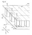
module 200 of the present embodiment, a conductive submount Sm is provided between theLD driver 110 and thefirst electrode 164. Therefore, the heat generated by thelaser diode 160 and theLD driver 110 can be dissipated, and the stress due to the difference in the coefficient of thermal expansion generated between thelaser diode 160 and theLD driver 110 can be relaxed.

E.第5実施形態:
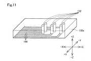
図10および図11に示すように、第5実施形態のモジュール200eは、第一電極パッド134および第二電極パッド136が、側壁部190Wのうち、レーザダイオード160の位置に対して出射方向DLとは逆側、すなわち−X方向側の側壁部190Wに備えられる点と、基台部130に代えて基台部130eを備える点と、第一配線電極195を備えない点と、コリメータレンズ194を備える点とで、第4実施形態のモジュール200と相違する。
E. Fifth embodiment:
As shown in FIGS. 10 and 11, in themodule 200e of the fifth embodiment, thefirst electrode pad 134 and thesecond electrode pad 136 have the emission direction DL with respect to the position of thelaser diode 160 in theside wall portion 190W. Is provided on the opposite side, that is, theside wall portion 190W on the −X direction side, thebase portion 130e is provided instead of thebase portion 130, thefirst wiring electrode 195 is not provided, and thecollimator lens 194 is provided. It differs from themodule 200 of the fourth embodiment in that it is provided.

第二電極パッド136は、図10に示すように、−X方向側の側壁部190Wの+Z方向側の端部に配置され、導電体のリッド180と当接される。第二電極パッド136は、リッド180と第三導電体170を介して第二電極162と電気的に接続され、−X方向側の側壁部190W上で第二接続部として機能する。第一電極パッド134は、−X方向側の側壁部190Wの−Z方向側の端部に配置される。 As shown in FIG. 10, thesecond electrode pad 136 is arranged at the end of theside wall portion 190W on the −X direction side on the + Z direction side, and is in contact with thelid 180 of the conductor. Thesecond electrode pad 136 is electrically connected to thesecond electrode 162 via thelid 180 and thethird conductor 170, and functions as the second connection portion on theside wall portion 190W on the −X direction side. Thefirst electrode pad 134 is arranged at the end portion of theside wall portion 190W on the −X direction side on the −Z direction side.

基台部130eは、いわゆるセラミック基板であり、図11に示すように、第一ビア状接続部132を備える点で、第4実施形態での基台部130と共通するが、更に、下面側に第二配線電極196を備える点で第4実施形態での基台部130と相違する。本実施形態において、基台部130eは、ビア状放熱部138と、第二ビア状接続部133および第三電極パッド135を備えないが、備えてもよい。 Thebase portion 130e is a so-called ceramic substrate, and as shown in FIG. 11, is common to thebase portion 130 in the fourth embodiment in that it includes the first via-shaped connectingportion 132, but is further on the lower surface side. It is different from thebase portion 130 in the fourth embodiment in that thesecond wiring electrode 196 is provided in thebase portion 130. In the present embodiment, thebase portion 130e does not include the via-shapedheat radiating portion 138, the second via-shaped connectingportion 133, and thethird electrode pad 135, but may be provided.

第二配線電極196は、基台部130eの下面側に備えられる導体配線である。第二配線電極196は、側壁部190Wに設けられる各第一電極パッド134と、各第一ビア状接続部132とを電気的に接続する。これにより、本実施形態において、第一電極パッド134は、第二配線電極196および第一ビア状接続部132を介してLDドライバ110に電気的に接続され、サブマウントSmを介して第二電極162に電気的に接続される。第一電極パッド134は、−X方向側の側壁部190Wで第一接続部として機能する。 Thesecond wiring electrode 196 is a conductor wiring provided on the lower surface side of thebase portion 130e. Thesecond wiring electrode 196 electrically connects eachfirst electrode pad 134 provided on theside wall portion 190W and each first via-shaped connectingportion 132. As a result, in the present embodiment, thefirst electrode pad 134 is electrically connected to theLD driver 110 via thesecond wiring electrode 196 and the first via-shaped connectingportion 132, and is electrically connected to theLD driver 110 via the submount Sm. It is electrically connected to 162. Thefirst electrode pad 134 functions as a first connection portion at theside wall portion 190W on the −X direction side.

次に、図12、図13を用いて、モジュール200eを備える半導体レーザ装置400eの構成について説明する。図12には、半導体レーザ装置400eに備えられる回路基板PBの+X方向側の表面が模式的に示されている。図12に示すように、本実施形態の半導体レーザ装置400eは、回路基板PB上に、複数のモジュール200eを備える。モジュール200eは、図12の例において9つ備えられる。 Next, the configuration of thesemiconductor laser device 400e including themodule 200e will be described with reference to FIGS. 12 and 13. FIG. 12 schematically shows the surface of the circuit board PB provided in thesemiconductor laser device 400e on the + X direction side. As shown in FIG. 12, thesemiconductor laser device 400e of the present embodiment includes a plurality ofmodules 200e on the circuit board PB. Ninemodules 200e are provided in the example of FIG.

上述したように、本実施形態のモジュール200eでは、第一電極パッド134および第二電極パッド136が、レーザダイオード160の位置に対して出射方向DLとは逆側である−X方向側の側壁部190Wに備えられる。図13に示すように、各モジュール200eは、第一電極パッド134と第二電極パッド136との一般的なリフロー工程によるはんだ付けによって回路基板PB上に実装される。これにより、第一接続部として機能する第一電極パッド134と、第二接続部として機能する第二電極パッド136とが、回路基板PB上の導体配線に当接された状態で回路基板PBの表面に実装される。実装された各モジュール200eのレーザ光の出射方向DLは、+X方向側にそれぞれ揃えられる。 As described above, in themodule 200e of the present embodiment, thefirst electrode pad 134 and thesecond electrode pad 136 are on the side wall portion on the −X direction side opposite to the emission direction DL with respect to the position of thelaser diode 160. Prepared for 190W. As shown in FIG. 13, eachmodule 200e is mounted on the circuit board PB by soldering thefirst electrode pad 134 and thesecond electrode pad 136 by a general reflow process. As a result, thefirst electrode pad 134 that functions as the first connection portion and thesecond electrode pad 136 that functions as the second connection portion of the circuit board PB are in contact with the conductor wiring on the circuit board PB. It is mounted on the surface. The emission direction DL of the laser beam of each of the mountedmodules 200e is aligned on the + X direction side.

図12および図13に示すように、各モジュール200eは、回路基板PBの表面にZ方向とY方向とのそれぞれにおいて互いに等間隔となるように規則的に配列され、いわゆる二次元アレイを構成している。 As shown in FIGS. 12 and 13, eachmodule 200e is regularly arranged on the surface of the circuit board PB so as to be evenly spaced from each other in the Z direction and the Y direction, respectively, forming a so-called two-dimensional array. ing.

図13に示すように、本実施形態の半導体レーザ装置400eは、各モジュール200eの出射方向DL側に、更にマイクロレンズアレイ300を備える。マイクロレンズアレイ300の構成は、第3実施形態でのマイクロレンズアレイ300と同様である。マイクロレンズアレイ300の各集光レンズは、各モジュール200eから出射されるレーザ光の光路のそれぞれに対応する位置に配置される。 As shown in FIG. 13, thesemiconductor laser device 400e of the present embodiment further includes amicrolens array 300 on the emission direction DL side of eachmodule 200e. The configuration of themicrolens array 300 is the same as that of themicrolens array 300 in the third embodiment. Each condensing lens of themicrolens array 300 is arranged at a position corresponding to each of the optical paths of the laser light emitted from eachmodule 200e.

本実施形態のモジュール200eによれば、第一電極パッド134と、第二電極パッド136とが、側壁部190Wのうち、レーザダイオード160の位置に対して出射方向DLとは逆側である−X方向側の側壁部190Wの外部側に備えられる。したがって、端面出射型のレーザダイオード160を、例えば、出射方向DLを半導体レーザ装置の回路基板の面方向に対して垂直な方向に一致させた状態で回路基板上に実装することができる。本実施形態のモジュール200eを複数備えることにより、回路基板上にアレイ状のレーザ光源を配置することができる。 According to themodule 200e of the present embodiment, thefirst electrode pad 134 and thesecond electrode pad 136 are on the side opposite to the emission direction DL with respect to the position of thelaser diode 160 in theside wall portion 190W. It is provided on the outer side of theside wall portion 190W on the directional side. Therefore, the end face emissiontype laser diode 160 can be mounted on the circuit board in a state where, for example, the emission direction DL is aligned with the direction perpendicular to the surface direction of the circuit board of the semiconductor laser apparatus. By providing a plurality ofmodules 200e of the present embodiment, an array of laser light sources can be arranged on the circuit board.

本実施形態のモジュール200eによれば、レーザダイオード160の出射方向DL側にコリメータレンズ194を備えるので、モジュール200eを平行光のレーザ光を出射するレーザ光源とすることができる。 According to themodule 200e of the present embodiment, since thecollimator lens 194 is provided on the DL side of thelaser diode 160 in the emission direction, themodule 200e can be used as a laser light source for emitting a laser beam of parallel light.

本実施形態の半導体レーザ装置400eによれば、複数の半導体レーザ光源モジュール200eのそれぞれは、レーザ光の出射方向DL側とは逆側となる第一接続部と第二接続部とが回路基板PBの導体配線に当接された状態で回路基板PBの表面に規則的な配列で実装される。したがって、回路基板PBの面方向に垂直な方向に複数のレーザ光を照射するレーザアレイを備えることができ、半導体レーザ装置400eを高出力化することができる。 According to thesemiconductor laser apparatus 400e of the present embodiment, in each of the plurality of semiconductor laserlight source modules 200e, the first connection portion and the second connection portion on the opposite side to the DL side in the emission direction of the laser light are the circuit board PB. It is mounted in a regular arrangement on the surface of the circuit board PB in a state of being in contact with the conductor wiring of. Therefore, it is possible to provide a laser array that irradiates a plurality of laser beams in a direction perpendicular to the plane direction of the circuit board PB, and it is possible to increase the output of thesemiconductor laser apparatus 400e.

本実施形態の半導体レーザ装置400eによれば、複数のモジュール200eから出射されるそれぞれのレーザ光の光路に対応するマイクロレンズアレイ300を備える。したがって、複数のモジュール200eのそれぞれから出射されるレーザ光を任意の光路に設定することができる。 According to thesemiconductor laser apparatus 400e of the present embodiment, themicrolens array 300 corresponding to the optical path of each laser beam emitted from the plurality ofmodules 200e is provided. Therefore, the laser light emitted from each of the plurality ofmodules 200e can be set to an arbitrary optical path.

F.他の実施形態:
(F1)上記第1実施形態では、第一導電体70のY方向側の端面70WをY方向側の側壁部90Wの外表面に露出させて第一接続部が構成され、平板状の第二導電体40(より具体的には金属層48)のY方向側の端面40WをY方向側の側壁部90Wの外表面に露出させて第二接続部が構成される。これに対して、第一導電体70、第二導電体40のいずれか一方の端面をY方向側の側壁部90Wの外表面に露出させる構成であってもよい。この場合において、第一導体面74または第二導体面44を第一接続部または第二接続部として構成してよい。
F. Other embodiments:
(F1) In the first embodiment, theend face 70W on the Y direction side of thefirst conductor 70 is exposed on the outer surface of theside wall portion 90W on the Y direction side to form the first connection portion, and the flat plate-shaped second The second connecting portion is formed by exposing theend face 40W on the Y direction side of the conductor 40 (more specifically, the metal layer 48) to the outer surface of theside wall portion 90W on the Y direction side. On the other hand, the end face of either thefirst conductor 70 or thesecond conductor 40 may be exposed on the outer surface of theside wall portion 90W on the Y direction side. In this case, thefirst conductor surface 74 or thesecond conductor surface 44 may be configured as the first connecting portion or the second connecting portion.

(F2)上記第2実施形態および第3実施形態では、第二導体面44は、下面金属層20または基台側金属層20cを介して第二電極62と電気的に接続される。これに対して、下面金属層20または基台側金属層20cに代えて、例えば基台部30の上面に形成された導体配線によって第二導体面44と第二電極62とが電気的に接続されてもよい。(F2) In the second embodiment and the third embodiment, thesecond conductor surface 44 is electrically connected to thesecond electrode 62 via the lowersurface metal layer 20 or the baseside metal layer 20c. On the other hand, instead of the lowersurface metal layer 20 or the baseside metal layer 20c, thesecond conductor surface 44 and thesecond electrode 62 are electrically connected by, for example, a conductor wiring formed on the upper surface of thebase portion 30. May be done.

(F3)上記第2実施形態および第3実施形態では、第一電極64は、導電体からなるリッド80を介して第一導体面74と電気的に接続される。これに対して非導電体からなるリッド80の下面に形成された導体配線によって第一電極64と第一導体面74とが電気的に接続されてもよい。(F3) In the second embodiment and the third embodiment, thefirst electrode 64 is electrically connected to thefirst conductor surface 74 via alid 80 made of a conductor. On the other hand, thefirst electrode 64 and thefirst conductor surface 74 may be electrically connected by a conductor wiring formed on the lower surface of thelid 80 made of a non-conductor.

(F4)上記各実施形態では、筐体90は側壁部90Wの一部に透光部92を備え、筐体190は側壁部190Wの一部に透光部192を備えるが、側壁部90Wや側壁部190Wをガラス等で構成することにより側壁部90Wや側壁部190Wの全体を透光部として構成してもよい。この形態の半導体レーザ光源モジュールによれば、レーザダイオードの出射方向とは逆側から出射されるレーザ光を取得することができる。(F4) In each of the above embodiments, thehousing 90 includes a light-transmittingportion 92 in a part of theside wall portion 90W, and thehousing 190 includes a light-transmittingportion 192 in a part of theside wall portion 190W. By configuring theside wall portion 190W with glass or the like, the entireside wall portion 90W or theside wall portion 190W may be configured as a light transmitting portion. According to the semiconductor laser light source module of this form, it is possible to acquire the laser beam emitted from the side opposite to the emission direction of the laser diode.

(F5)上記第3実施形態の半導体レーザ装置400cでは、各モジュール100cは、回路基板PBの表面に、Z方向とY方向とのそれぞれにおいて互いに等間隔となるように規則的に配列される。これに対して、各モジュール100cは、図14に示すように、回路基板PBの表面に、互い違いに配置されるいわゆる千鳥状の配置により規則的な配列で実装されてもよい。この形態の半導体レーザ装置400cによれば、各モジュール100cを高密度化し、半導体レーザ装置400cのレーザ光の分解能を高くすることができる。(F5) In thesemiconductor laser apparatus 400c of the third embodiment, themodules 100c are regularly arranged on the surface of the circuit board PB so as to be evenly spaced from each other in the Z direction and the Y direction. On the other hand, as shown in FIG. 14, eachmodule 100c may be mounted on the surface of the circuit board PB in a regular arrangement by so-called staggered arrangement. According to thesemiconductor laser device 400c of this form, the density of eachmodule 100c can be increased, and the resolution of the laser light of thesemiconductor laser device 400c can be increased.

(F6)上記第5実施形態の半導体レーザ装置400eでは、各モジュール200eは、回路基板PBの表面に、Z方向とY方向とのそれぞれにおいて互いに等間隔となるように規則的に配列される。これに対して、各モジュール200eは、図15に示すように、回路基板PBの表面に、互い違いに配置されるいわゆる千鳥状の配置により規則的な配列で実装されてもよい。この形態の半導体レーザ装置400eによれば、各モジュール200eを高密度化し、半導体レーザ装置400eによるレーザ光の分解能を高くすることができる。(F6) In thesemiconductor laser apparatus 400e of the fifth embodiment, themodules 200e are regularly arranged on the surface of the circuit board PB so as to be evenly spaced from each other in the Z direction and the Y direction. On the other hand, as shown in FIG. 15, eachmodule 200e may be mounted on the surface of the circuit board PB in a regular arrangement by so-called staggered arrangement. According to thesemiconductor laser device 400e of this form, eachmodule 200e can be densified to increase the resolution of the laser beam by thesemiconductor laser device 400e.

本開示は、上述の実施形態や変形例に限られるものではなく、その趣旨を逸脱しない範囲において種々の構成で実現することができる。例えば、発明の概要の欄に記載した各形態中の技術的特徴に対応する実施形態、変形例中の技術的特徴は、上述の課題の一部又は全部を解決するために、あるいは、上述の効果の一部又は全部を達成するために、適宜、差し替えや、組み合わせを行うことが可能である。また、その技術的特徴が本明細書中に必須なものとして説明されていなければ、適宜、削除することが可能である。 The present disclosure is not limited to the above-described embodiments and modifications, and can be realized with various configurations without departing from the spirit of the present disclosure. For example, the embodiments corresponding to the technical features in each of the embodiments described in the column of the outline of the invention, the technical features in the modified examples are used to solve some or all of the above-mentioned problems, or the above-mentioned above. It is possible to replace or combine them as appropriate to achieve some or all of the effects. Further, if the technical feature is not described as essential in the present specification, it can be appropriately deleted.

40,40b 第二導電体、60、160 レーザダイオード、62,162 第二電極、63,163 半導体層、64,164 第一電極、70,70b 第一導電体、90 筐体、90W,190W 側壁部、92,192 透光部、100,100b,100c,200,200e 半導体レーザ光源モジュール、110 LDドライバ、130,130e 基台部、134 第一電極パッド、136 第二電極パッド、170 第三導電体、40,40b 2nd conductor, 60,160 laser diode, 62,162 2nd electrode, 63,163 semiconductor layer, 64,164 1st electrode, 70,70b 1st conductor, 90 housing, 90W, 190W side wall Unit, 92,192 Translucent part, 100, 100b, 100c, 200, 200e Semiconductor laser light source module, 110 LD driver, 130, 130e base part, 134 1st electrode pad, 136 2nd electrode pad, 170 3rd conductive body,

Claims (22)

Translated fromJapanese
半導体レーザ光源モジュール(100,100b,100c)であって、
活性層を含む半導体層(63)の一方の面側に形成された第一電極(64)と、前記活性層の他方の面側に形成された第二電極(62)とを備える端面出射型のレーザダイオード(60)と、
前記レーザダイオードを囲む側壁部(90W)を有し、前記側壁部のうち少なくとも一部にレーザ光を透過する透光部(92)を備える筐体(90)と、
前記第一電極に当接される第一導電体(70,70b)と、
前記第二電極に当接される第二導電体(40,40b)と、
前記側壁部の外部側に設けられ、前記第一導電体と電気的に接続される第一接続部と、
前記側壁部の外部側に設けられ、前記第二導電体と電気的に接続される第二接続部と、を備える
半導体レーザ光源モジュール。
A semiconductor laser light source module (100, 100b, 100c).
An end face ejection type including a first electrode (64) formed on one surface side of a semiconductor layer (63) including an active layer and a second electrode (62) formed on the other surface side of the active layer. Laser diode (60) and
A housing (90) having a side wall portion (90 W) surrounding the laser diode and having a translucent portion (92) that transmits laser light at least a part of the side wall portion.
The first conductor (70, 70b) abutting on the first electrode and
The second conductors (40, 40b) that come into contact with the second electrode and
A first connection portion provided on the outer side of the side wall portion and electrically connected to the first conductor,
A semiconductor laser light source module including a second connecting portion provided on the outer side of the side wall portion and electrically connected to the second conductor.
前記第一導電体は、平板状の金属層を含み、
前記第一導電体に含まれる前記平板状の金属層の端面(70W)が、前記側壁部の外部側に露出して前記第一接続部として機能する、請求項1に記載の半導体レーザ光源モジュール。
The first conductor includes a flat metal layer and contains a flat metal layer.
The semiconductor laser light source module according to claim 1, wherein the end surface (70 W) of the flat metal layer contained in the first conductor is exposed to the outer side of the side wall portion and functions as the first connection portion. ..
更に、前記側壁部の外部側に、前記側壁部の厚みよりも小さい厚みを有する第一導体面(74)であって、前記第一導電体と電気的に接続される第一導体面を備え、
前記第一導体面の外部側の表面が前記第一接続部として機能する、請求項1に記載の半導体レーザ光源モジュール。
Further, on the outer side of the side wall portion, a first conductor surface (74) having a thickness smaller than the thickness of the side wall portion and which is electrically connected to the first conductor is provided. ,
The semiconductor laser light source module according to claim 1, wherein the outer surface of the first conductor surface functions as the first connection portion.
前記第二導電体は、平板状の金属層(48)を含み、
前記第二導電体に含まれる前記平板状の金属層の端面(40W)が、前記側壁部の外部側に露出して前記第二接続部として機能する、請求項1から請求項3までのいずれか一項に記載の半導体レーザ光源モジュール。
The second conductor includes a flat metal layer (48).
Any of claims 1 to 3, wherein the end face (40 W) of the flat metal layer contained in the second conductor is exposed to the outer side of the side wall portion and functions as the second connecting portion. The semiconductor laser light source module according to claim 1.
更に、前記側壁部の外部側に、前記側壁部の厚みよりも小さい厚みを有する第二導体面(44)であって、前記第二導電体と電気的に接続される第二導体面を備え、
前記第二導体面の外部側の表面が前記第二接続部として機能する、請求項1から請求項3までのいずれか一項に記載の半導体レーザ光源モジュール。
Further, on the outer side of the side wall portion, a second conductor surface (44) having a thickness smaller than the thickness of the side wall portion, which is electrically connected to the second conductor, is provided. ,
The semiconductor laser light source module according to any one of claims 1 to 3, wherein the outer surface of the second conductor surface functions as the second connecting portion.
更に、前記第二導電体の前記第一導電体と当接する側とは逆側に、前記第二導電体と当接するセラミック製の基台部(30,30c)を備える、請求項1から請求項5のいずれか一項に記載の半導体レーザ光源モジュール。 Further, according to claim 1, a ceramic base portion (30, 30c) that comes into contact with the second conductor is provided on the side opposite to the side of the second conductor that comes into contact with the first conductor. Item 5. The semiconductor laser light source module according to any one of Item 5. 請求項6に記載の半導体レーザ光源モジュールであって、
更に、前記基台部の前記第二導電体と当接する側とは逆側に基台側金属層(20c)を備え、
前記基台部は、導電性を有するビア状接続部(32)を備え、
前記基台側金属層は、前記第二接続部と電気的に接続されるとともに、前記ビア状接続部を介して前記第二導電体と電気的に接続される、
半導体レーザ光源モジュール。
The semiconductor laser light source module according to claim 6.
Further, a base side metal layer (20c) is provided on the side of the base portion opposite to the side that comes into contact with the second conductor.
The base portion includes a conductive via-shaped connecting portion (32).
The base-side metal layer is electrically connected to the second connecting portion and is electrically connected to the second conductor via the via-shaped connecting portion.
Semiconductor laser light source module.
更に、前記透光部の外表面上にコリメータレンズ(94)を備える、請求項1から請求項7までのいずれか一項に記載の半導体レーザ光源モジュール。 The semiconductor laser light source module according to any one of claims 1 to 7, further comprising a collimator lens (94) on the outer surface of the translucent portion. 前記第一接続部と前記第二接続部とは、前記レーザダイオードの位置に対して、前記レーザ光の出射方向側とは逆側となる前記側壁部の外部側に備えられる、請求項1から請求項8までのいずれか一項に記載の半導体レーザ光源モジュール。 From claim 1, the first connection portion and the second connection portion are provided on the outer side of the side wall portion which is opposite to the position of the laser diode in the emission direction side of the laser beam. The semiconductor laser light source module according to any one of claims 8. 請求項9に記載の半導体レーザ光源モジュールであって、複数の半導体レーザ光源モジュールと、
前記複数の半導体レーザ光源モジュールに電流を供給する回路基板(PB)と、を備え、
前記複数の半導体レーザ光源モジュールのそれぞれは、前記側壁部の外部側に備えられる前記第一接続部と前記第二接続部とが前記回路基板の導体配線に当接された状態で、前記回路基板の表面に規則的な配列で実装される、
半導体レーザ装置。
The semiconductor laser light source module according to claim 9, wherein a plurality of semiconductor laser light source modules and
A circuit board (PB) that supplies a current to the plurality of semiconductor laser light source modules is provided.
Each of the plurality of semiconductor laser light source modules has the circuit board in a state where the first connection portion and the second connection portion provided on the outer side of the side wall portion are in contact with the conductor wiring of the circuit board. Implemented in a regular array on the surface of
Semiconductor laser device.
請求項10に記載の半導体レーザ装置であって、
前記複数の半導体レーザ光源モジュールは、前記回路基板の表面に互い違いに配置されることにより前記規則的な配列で実装される、
半導体レーザ装置。
The semiconductor laser device according to claim 10.
The plurality of semiconductor laser light source modules are mounted in the regular arrangement by alternately arranging them on the surface of the circuit board.
Semiconductor laser device.
請求項10または請求項11に記載の半導体レーザ装置であって、
更に、前記規則的に配列された前記複数の半導体レーザ光源モジュールから出射されるそれぞれのレーザ光の光路に対応するマイクロレンズアレイ(300)を備える、
半導体レーザ装置。
The semiconductor laser device according to claim 10 or 11.
Further, the microlens array (300) corresponding to the optical path of each laser beam emitted from the plurality of regularly arranged semiconductor laser light source modules is provided.
Semiconductor laser device.
半導体レーザ光源モジュール(200,200e)であって、
活性層を含む半導体層(163)の一方の面側に形成された第一電極(164)と、前記活性層の他方の面側に形成された第二電極(162)とを備える端面出射型のレーザダイオード(160)と、
前記レーザダイオードを囲む側壁部(190W)を有し、前記側壁部のうち少なくとも一部にレーザ光を透過する透光部(192)を備える筐体(190)と、
前記第一電極と電気的に接続され、前記レーザダイオードを駆動する平板状のLDドライバ(110)と、
前記レーザダイオードを挟んで前記LDドライバの一方の面側と対向するように配され、前記第二電極に当接されて前記レーザダイオードと電気的に接続される導電体(170)と、
前記LDドライバの他方の面側に当接されるセラミック製の基台部(130,130e)と、
前記筐体の外部側に配置される第一電極パッド(134)であって、前記LDドライバと電気的に接続される第一電極パッドと、
前記筐体の外部側に配置される第二電極パッド(136)であって、前記導電体と電気的に接続される第二電極パッドと、を備える
半導体レーザ光源モジュール。
It is a semiconductor laser light source module (200, 200e).
An end face emission type including a first electrode (164) formed on one surface side of a semiconductor layer (163) including an active layer and a second electrode (162) formed on the other surface side of the active layer. Laser diode (160) and
A housing (190) having a side wall portion (190 W) surrounding the laser diode and having a translucent portion (192) that transmits laser light at least a part of the side wall portion.
A flat-plate LD driver (110) that is electrically connected to the first electrode and drives the laser diode,
A conductor (170) arranged so as to face one surface side of the LD driver across the laser diode, abutting on the second electrode, and electrically connected to the laser diode.
A ceramic base portion (130, 130e) abutting on the other surface side of the LD driver, and
A first electrode pad (134) arranged on the outer side of the housing, which is electrically connected to the LD driver, and a first electrode pad.
A semiconductor laser light source module including a second electrode pad (136) arranged on the outer side of the housing, the second electrode pad being electrically connected to the conductor.
請求項13に記載の半導体レーザ光源モジュールであって、
前記基台部のうち前記LDドライバと当接される面の少なくとも一部と当接されて、前記LDドライバの熱を放熱するビア状放熱部(138)を備える
半導体レーザ光源モジュール。
The semiconductor laser light source module according to claim 13.
A semiconductor laser light source module including a via-shaped heat radiating portion (138) that is in contact with at least a part of a surface of the base portion that is in contact with the LD driver and dissipates heat from the LD driver.
請求項13または請求項14に記載の半導体レーザ光源モジュールであって、
前記基台部は、前記LDドライバと前記第一電極パッドとを電気的に接続する導電性のビア状接続部(132)を備える
半導体レーザ光源モジュール。
The semiconductor laser light source module according to claim 13 or 14.
The base portion is a semiconductor laser light source module including a conductive via-shaped connecting portion (132) that electrically connects the LD driver and the first electrode pad.
前記LDドライバは、前記一方の面側にドライバ電極(112)を有し、前記ドライバ電極と前記第一電極とが互いに電気的に接続される
請求項13から請求項15までのいずれか一項に記載の半導体レーザ光源モジュール。
The LD driver has a driver electrode (112) on one surface side thereof, and any one of claims 13 to 15 in which the driver electrode and the first electrode are electrically connected to each other. The semiconductor laser light source module according to.
更に、前記LDドライバと前記第一電極との間に導電性のサブマウント(Sm)を備え、
前記サブマウントは、前記ドライバ電極と当接して前記LDドライバと電気的に接続されるとともに、前記第一電極と当接して前記レーザダイオードと電気的に接続される
請求項16に記載の半導体レーザ光源モジュール。
Further, a conductive submount (Sm) is provided between the LD driver and the first electrode.
The semiconductor laser according to claim 16, wherein the submount is in contact with the driver electrode and electrically connected to the LD driver, and is in contact with the first electrode and electrically connected to the laser diode. Light source module.
更に、前記透光部の外表面上にコリメータレンズ(194)を備える、請求項13から請求項17までのいずれか一項に記載の半導体レーザ光源モジュール。 The semiconductor laser light source module according to any one of claims 13 to 17, further comprising a collimator lens (194) on the outer surface of the translucent portion. 前記第一電極パッドと、前記第二電極パッドとは、前記側壁部のうち、前記レーザダイオードの位置に対して、前記レーザ光の出射方向側とは逆側となる前記側壁部の外部側に備えられる、請求項13から請求項18までのいずれか一項に記載の半導体レーザ光源モジュール。 The first electrode pad and the second electrode pad are located on the outer side of the side wall portion of the side wall portion, which is opposite to the position of the laser diode in the emission direction side of the laser beam. The semiconductor laser light source module according to any one of claims 13 to 18, which is provided. 請求項19に記載の半導体レーザ光源モジュールであって、複数の半導体レーザ光源モジュールと、
前記複数の半導体レーザ光源モジュールに電流を供給する回路基板(PB)と、を備え、
前記複数の半導体レーザ光源モジュールのそれぞれは、前記側壁部の外部側に備えられる前記第一電極パッドと前記第二電極パッドとが前記回路基板の導体配線に当接された状態で、前記回路基板の表面に規則的な配列で実装される、
半導体レーザ装置(400e)。
The semiconductor laser light source module according to claim 19, wherein a plurality of semiconductor laser light source modules and
A circuit board (PB) that supplies a current to the plurality of semiconductor laser light source modules is provided.
Each of the plurality of semiconductor laser light source modules has the circuit board in a state where the first electrode pad and the second electrode pad provided on the outer side of the side wall portion are in contact with the conductor wiring of the circuit board. Implemented in a regular arrangement on the surface of
Semiconductor laser device (400e).
請求項20に記載の半導体レーザ装置であって、
前記複数の半導体レーザ光源モジュールは、前記回路基板の表面に互い違いに配置されることにより前記規則的な配列で実装される、
半導体レーザ装置。
The semiconductor laser device according to claim 20.
The plurality of semiconductor laser light source modules are mounted in the regular arrangement by alternately arranging them on the surface of the circuit board.
Semiconductor laser device.
請求項20または請求項21に記載の半導体レーザ装置であって、
前記規則的に配列された前記複数の半導体レーザ光源モジュールから出射されるそれぞれのレーザ光の光路に対応するマイクロレンズアレイ(300)を備える、
半導体レーザ装置。
The semiconductor laser device according to claim 20 or 21.
A microlens array (300) corresponding to an optical path of each laser light emitted from the plurality of regularly arranged semiconductor laser light source modules is provided.
Semiconductor laser device.
JP2019114331A2019-06-202019-06-20 Semiconductor laser light source module, semiconductor laser deviceActiveJP7275894B2 (en)

Priority Applications (1)

Application NumberPriority DateFiling DateTitle
JP2019114331AJP7275894B2 (en)2019-06-202019-06-20 Semiconductor laser light source module, semiconductor laser device

Applications Claiming Priority (1)

Application NumberPriority DateFiling DateTitle
JP2019114331AJP7275894B2 (en)2019-06-202019-06-20 Semiconductor laser light source module, semiconductor laser device

Publications (2)

Publication NumberPublication Date
JP2021002546Atrue JP2021002546A (en)2021-01-07
JP7275894B2 JP7275894B2 (en)2023-05-18

Family

ID=73995101

Family Applications (1)

Application NumberTitlePriority DateFiling Date
JP2019114331AActiveJP7275894B2 (en)2019-06-202019-06-20 Semiconductor laser light source module, semiconductor laser device

Country Status (1)

CountryLink
JP (1)JP7275894B2 (en)

Cited By (3)

* Cited by examiner, † Cited by third party
Publication numberPriority datePublication dateAssigneeTitle
WO2022230339A1 (en)*2021-04-272022-11-03日亜化学工業株式会社Light source device
JP2023076215A (en)*2021-11-222023-06-01スタンレー電気株式会社 Surface emitting module and manufacturing method thereof
JP2023184626A (en)*2019-10-232023-12-28日亜化学工業株式会社 light source device

Citations (7)

* Cited by examiner, † Cited by third party
Publication numberPriority datePublication dateAssigneeTitle
JPH11177181A (en)*1997-12-081999-07-02Toshiba Corp Two-dimensional semiconductor laser array unit, two-dimensional semiconductor laser array, and laser processing apparatus using the same
JP2009514199A (en)*2005-10-272009-04-02リモ パテントフェルヴァルトゥング ゲーエムベーハー ウント コー.カーゲー Semiconductor laser device
JP2012209286A (en)*2011-03-292012-10-25Hitachi LtdOptical module
US20170117683A1 (en)*2015-10-222017-04-27Northrup Grumman Space and Mission Systems Corp.Thermally conductive, current carrying, electrically isolated submount for laser diode arrays
WO2018030486A1 (en)*2016-08-102018-02-15京セラ株式会社Package for mounting electrical element, array package and electrical device
JP2018507552A (en)*2015-02-242018-03-15イェノプティック レーザー ゲーエムベーハーJenoptik Laser Gmbh Diode laser manufacturing method and diode laser
US20180278011A1 (en)*2017-03-232018-09-27Infineon Technologies AgLaser diode module

Patent Citations (7)

* Cited by examiner, † Cited by third party
Publication numberPriority datePublication dateAssigneeTitle
JPH11177181A (en)*1997-12-081999-07-02Toshiba Corp Two-dimensional semiconductor laser array unit, two-dimensional semiconductor laser array, and laser processing apparatus using the same
JP2009514199A (en)*2005-10-272009-04-02リモ パテントフェルヴァルトゥング ゲーエムベーハー ウント コー.カーゲー Semiconductor laser device
JP2012209286A (en)*2011-03-292012-10-25Hitachi LtdOptical module
JP2018507552A (en)*2015-02-242018-03-15イェノプティック レーザー ゲーエムベーハーJenoptik Laser Gmbh Diode laser manufacturing method and diode laser
US20170117683A1 (en)*2015-10-222017-04-27Northrup Grumman Space and Mission Systems Corp.Thermally conductive, current carrying, electrically isolated submount for laser diode arrays
WO2018030486A1 (en)*2016-08-102018-02-15京セラ株式会社Package for mounting electrical element, array package and electrical device
US20180278011A1 (en)*2017-03-232018-09-27Infineon Technologies AgLaser diode module

Cited By (4)

* Cited by examiner, † Cited by third party
Publication numberPriority datePublication dateAssigneeTitle
JP2023184626A (en)*2019-10-232023-12-28日亜化学工業株式会社 light source device
JP7525811B2 (en)2019-10-232024-07-31日亜化学工業株式会社 Light source
WO2022230339A1 (en)*2021-04-272022-11-03日亜化学工業株式会社Light source device
JP2023076215A (en)*2021-11-222023-06-01スタンレー電気株式会社 Surface emitting module and manufacturing method thereof

Also Published As

Publication numberPublication date
JP7275894B2 (en)2023-05-18

Similar Documents

PublicationPublication DateTitle
KR102503462B1 (en) Mounting of LED elements on a flat carrier
JP7338713B2 (en) Carrier mounting structure
CN102422193B (en)Optical subassembly with optical device having ceramic pacakge
JP7275894B2 (en) Semiconductor laser light source module, semiconductor laser device
JPWO2007004450A1 (en) Linear light source device, surface light emitting device, and liquid crystal display device
CN110579751A (en)Transmitting system applicable to laser radar, laser radar and laser transmitting method
US20220109285A1 (en)Semiconductor laser light source module, semiconductor laser apparatus
CN111146690A (en) A kind of laser module and preparation method thereof
CN111934189A (en)Light emitting module and packaging method thereof
WO2021072752A1 (en)Laser diode encapsulation module, distance detection apparatus, and electronic device
CN217507921U (en)Laser module
CN112636160A (en)Laser device
CN217766830U (en)Laser emitting module and laser radar device
KR102669828B1 (en)Laser Diode package
JP4951691B2 (en) Optical transmission module and optical communication device using the same
JP2006156643A (en)Surface-mounted light-emitting diode
US20240372315A1 (en)Semiconductor light emitting device
JP7542466B2 (en) Optical Modules
JP2019075460A (en)Semiconductor light emitting element and semiconductor light emitting device
JP2018018995A (en) Optical module
CN217469099U (en)Laser system
CN115152331A (en)Substrate and semiconductor laser
CN110488562A (en)Integrated laser projection mould group
JP2013030549A (en)Light emitting module and member for chip component mounting
JP7544304B1 (en) Optical Modules and Transceivers

Legal Events

DateCodeTitleDescription
A621Written request for application examination

Free format text:JAPANESE INTERMEDIATE CODE: A621

Effective date:20220413

A977Report on retrieval

Free format text:JAPANESE INTERMEDIATE CODE: A971007

Effective date:20221223

A131Notification of reasons for refusal

Free format text:JAPANESE INTERMEDIATE CODE: A131

Effective date:20230110

A521Request for written amendment filed

Free format text:JAPANESE INTERMEDIATE CODE: A523

Effective date:20230308

A131Notification of reasons for refusal

Free format text:JAPANESE INTERMEDIATE CODE: A131

Effective date:20230314

A521Request for written amendment filed

Free format text:JAPANESE INTERMEDIATE CODE: A523

Effective date:20230328

TRDDDecision of grant or rejection written
A01Written decision to grant a patent or to grant a registration (utility model)

Free format text:JAPANESE INTERMEDIATE CODE: A01

Effective date:20230404

A61First payment of annual fees (during grant procedure)

Free format text:JAPANESE INTERMEDIATE CODE: A61

Effective date:20230417

R151Written notification of patent or utility model registration

Ref document number:7275894

Country of ref document:JP

Free format text:JAPANESE INTERMEDIATE CODE: R151


[8]ページ先頭

©2009-2025 Movatter.jp