JP2020514783A - Waveguide with uniform output illumination - Google Patents
Waveguide with uniform output illuminationDownload PDFInfo
- Publication number
- JP2020514783A JP2020514783AJP2019529860AJP2019529860AJP2020514783AJP 2020514783 AJP2020514783 AJP 2020514783AJP 2019529860 AJP2019529860 AJP 2019529860AJP 2019529860 AJP2019529860 AJP 2019529860AJP 2020514783 AJP2020514783 AJP 2020514783A
- Authority
- JP
- Japan
- Prior art keywords
- grating
- light
- optics
- input
- banding
- Prior art date
- Legal status (The legal status is an assumption and is not a legal conclusion. Google has not performed a legal analysis and makes no representation as to the accuracy of the status listed.)
- Pending
Links
Images


Classifications
- G—PHYSICS
- G02—OPTICS
- G02B—OPTICAL ELEMENTS, SYSTEMS OR APPARATUS
- G02B6/00—Light guides; Structural details of arrangements comprising light guides and other optical elements, e.g. couplings
- G02B6/0001—Light guides; Structural details of arrangements comprising light guides and other optical elements, e.g. couplings specially adapted for lighting devices or systems
- G02B6/0011—Light guides; Structural details of arrangements comprising light guides and other optical elements, e.g. couplings specially adapted for lighting devices or systems the light guides being planar or of plate-like form
- G02B6/0013—Means for improving the coupling-in of light from the light source into the light guide
- G02B6/0023—Means for improving the coupling-in of light from the light source into the light guide provided by one optical element, or plurality thereof, placed between the light guide and the light source, or around the light source
- G—PHYSICS
- G02—OPTICS
- G02B—OPTICAL ELEMENTS, SYSTEMS OR APPARATUS
- G02B27/00—Optical systems or apparatus not provided for by any of the groups G02B1/00 - G02B26/00, G02B30/00
- G02B27/0081—Optical systems or apparatus not provided for by any of the groups G02B1/00 - G02B26/00, G02B30/00 with means for altering, e.g. enlarging, the entrance or exit pupil
- G—PHYSICS
- G02—OPTICS
- G02B—OPTICAL ELEMENTS, SYSTEMS OR APPARATUS
- G02B27/00—Optical systems or apparatus not provided for by any of the groups G02B1/00 - G02B26/00, G02B30/00
- G02B27/01—Head-up displays
- G02B27/0101—Head-up displays characterised by optical features
- G—PHYSICS
- G02—OPTICS
- G02B—OPTICAL ELEMENTS, SYSTEMS OR APPARATUS
- G02B27/00—Optical systems or apparatus not provided for by any of the groups G02B1/00 - G02B26/00, G02B30/00
- G02B27/01—Head-up displays
- G02B27/0101—Head-up displays characterised by optical features
- G02B27/0103—Head-up displays characterised by optical features comprising holographic elements
- G—PHYSICS
- G02—OPTICS
- G02B—OPTICAL ELEMENTS, SYSTEMS OR APPARATUS
- G02B27/00—Optical systems or apparatus not provided for by any of the groups G02B1/00 - G02B26/00, G02B30/00
- G02B27/01—Head-up displays
- G02B27/017—Head mounted
- G02B27/0172—Head mounted characterised by optical features
- G—PHYSICS
- G02—OPTICS
- G02B—OPTICAL ELEMENTS, SYSTEMS OR APPARATUS
- G02B6/00—Light guides; Structural details of arrangements comprising light guides and other optical elements, e.g. couplings
- G02B6/0001—Light guides; Structural details of arrangements comprising light guides and other optical elements, e.g. couplings specially adapted for lighting devices or systems
- G02B6/0011—Light guides; Structural details of arrangements comprising light guides and other optical elements, e.g. couplings specially adapted for lighting devices or systems the light guides being planar or of plate-like form
- G02B6/0013—Means for improving the coupling-in of light from the light source into the light guide
- G02B6/0015—Means for improving the coupling-in of light from the light source into the light guide provided on the surface of the light guide or in the bulk of it
- G02B6/0016—Grooves, prisms, gratings, scattering particles or rough surfaces
- G—PHYSICS
- G02—OPTICS
- G02B—OPTICAL ELEMENTS, SYSTEMS OR APPARATUS
- G02B6/00—Light guides; Structural details of arrangements comprising light guides and other optical elements, e.g. couplings
- G02B6/0001—Light guides; Structural details of arrangements comprising light guides and other optical elements, e.g. couplings specially adapted for lighting devices or systems
- G02B6/0011—Light guides; Structural details of arrangements comprising light guides and other optical elements, e.g. couplings specially adapted for lighting devices or systems the light guides being planar or of plate-like form
- G02B6/0033—Means for improving the coupling-out of light from the light guide
- G02B6/0035—Means for improving the coupling-out of light from the light guide provided on the surface of the light guide or in the bulk of it
- G—PHYSICS
- G02—OPTICS
- G02B—OPTICAL ELEMENTS, SYSTEMS OR APPARATUS
- G02B6/00—Light guides; Structural details of arrangements comprising light guides and other optical elements, e.g. couplings
- G02B6/0001—Light guides; Structural details of arrangements comprising light guides and other optical elements, e.g. couplings specially adapted for lighting devices or systems
- G02B6/0011—Light guides; Structural details of arrangements comprising light guides and other optical elements, e.g. couplings specially adapted for lighting devices or systems the light guides being planar or of plate-like form
- G02B6/0033—Means for improving the coupling-out of light from the light guide
- G02B6/0058—Means for improving the coupling-out of light from the light guide varying in density, size, shape or depth along the light guide
- G02B6/0061—Means for improving the coupling-out of light from the light guide varying in density, size, shape or depth along the light guide to provide homogeneous light output intensity
- G—PHYSICS
- G02—OPTICS
- G02B—OPTICAL ELEMENTS, SYSTEMS OR APPARATUS
- G02B6/00—Light guides; Structural details of arrangements comprising light guides and other optical elements, e.g. couplings
- G02B6/0001—Light guides; Structural details of arrangements comprising light guides and other optical elements, e.g. couplings specially adapted for lighting devices or systems
- G02B6/0011—Light guides; Structural details of arrangements comprising light guides and other optical elements, e.g. couplings specially adapted for lighting devices or systems the light guides being planar or of plate-like form
- G02B6/0075—Arrangements of multiple light guides
- G02B6/0076—Stacked arrangements of multiple light guides of the same or different cross-sectional area
- G—PHYSICS
- G02—OPTICS
- G02B—OPTICAL ELEMENTS, SYSTEMS OR APPARATUS
- G02B27/00—Optical systems or apparatus not provided for by any of the groups G02B1/00 - G02B26/00, G02B30/00
- G02B27/01—Head-up displays
- G02B27/0101—Head-up displays characterised by optical features
- G02B2027/0112—Head-up displays characterised by optical features comprising device for genereting colour display
- G02B2027/0114—Head-up displays characterised by optical features comprising device for genereting colour display comprising dichroic elements
- G—PHYSICS
- G02—OPTICS
- G02B—OPTICAL ELEMENTS, SYSTEMS OR APPARATUS
- G02B27/00—Optical systems or apparatus not provided for by any of the groups G02B1/00 - G02B26/00, G02B30/00
- G02B27/01—Head-up displays
- G02B27/0101—Head-up displays characterised by optical features
- G02B2027/0112—Head-up displays characterised by optical features comprising device for genereting colour display
- G02B2027/0116—Head-up displays characterised by optical features comprising device for genereting colour display comprising devices for correcting chromatic aberration
- G—PHYSICS
- G02—OPTICS
- G02B—OPTICAL ELEMENTS, SYSTEMS OR APPARATUS
- G02B27/00—Optical systems or apparatus not provided for by any of the groups G02B1/00 - G02B26/00, G02B30/00
- G02B27/01—Head-up displays
- G02B27/017—Head mounted
- G02B27/0172—Head mounted characterised by optical features
- G02B2027/0174—Head mounted characterised by optical features holographic
Landscapes
- Physics & Mathematics (AREA)
- General Physics & Mathematics (AREA)
- Optics & Photonics (AREA)
- Diffracting Gratings Or Hologram Optical Elements (AREA)
- Optical Modulation, Optical Deflection, Nonlinear Optics, Optical Demodulation, Optical Logic Elements (AREA)
Abstract
Translated fromJapaneseDescription
Translated fromJapanese本開示は、導波管デバイスに関し、より具体的には、均一出力照明を有する、導波管に関する。 The present disclosure relates to waveguide devices, and more particularly to waveguides having uniform output illumination.
導波管光学は、現在、複数の光学機能を薄くて透明な軽量基板の中に統合する導波管デバイスの能力が非常に重要である、ある範囲のディスプレイおよびセンサ用途のために検討されている。本新しいアプローチは、航空および道路交通のための拡張現実(AR)および仮想現実(VR)、コンパクトヘッドアップディスプレイ(HUD)のための眼近接ディスプレイと、バイオメトリックおよびレーザレーダ(LIDAR)用途のためのセンサとを含む、新しい製品開発を促している。 Waveguide optics is currently being considered for a range of display and sensor applications where the ability of the waveguide device to integrate multiple optical functions into a thin, transparent, lightweight substrate is very important. There is. The new approach is used for augmented reality (AR) and virtual reality (VR), near-eye displays for compact head-up displays (HUD) for air and road traffic, and for biometric and laser radar (LIDAR) applications. It promotes the development of new products, including new sensors.
導波管デバイスは、HMDおよびHUDにおいて魅力的である、多くの特徴をもたらす。それらは、薄くて透明であることである。広視野は、複数のホログラムを記録し、各ホログラムによって形成される視野領域をタイル化することによって取得されることができる。 Waveguide devices offer many features that make them attractive in HMDs and HUDs. They are thin and transparent. A wide field of view can be obtained by recording multiple holograms and tiling the field of view formed by each hologram.
いくつかの実施形態は、少なくとも1つの光学基板と、少なくとも1つの光源と、少なくとも1つの光結合器と、少なくとも1つの光抽出器と、バンディング除去光学とを含む、導波管デバイスを対象とする。少なくとも1つの光結合器は、入力格子において決定されるような一意のTIR角度が各光入射角によって画定されるように、ある角度帯域幅を伴う光源からの入射光を少なくとも1つの光学基板内の全内部反射(TIR)の中に結合することが可能である。少なくとも1つの光抽出器は、光学基板からの光を抽出する。バンディング除去光学は、抽出された光が軽減されたバンディングを有する略平坦照明プロファイルであるように、照明された瞳のバンディング効果を軽減することが可能である。 Some embodiments are directed to waveguide devices that include at least one optical substrate, at least one light source, at least one light combiner, at least one light extractor, and banding removal optics. To do. At least one optocoupler directs incident light from a light source with a certain angular bandwidth into at least one optical substrate such that a unique TIR angle as determined at the input grating is defined by each light incident angle. Can be coupled into the total internal reflection (TIR) of the. At least one light extractor extracts light from the optical substrate. The banding removal optics can mitigate the banding effect of the illuminated pupil such that the extracted light is a substantially flat illumination profile with reduced banding.
より多くの実施形態では、抽出された光は、10%未満の空間非均一性を有する。 In more embodiments, the extracted light has a spatial non-uniformity of less than 10%.
さらなる実施形態では、抽出された光は、20%未満の空間非均一性を有する。 In a further embodiment, the extracted light has a spatial non-uniformity of less than 20%.
さらにより多くの実施形態では、バンディング除去光学は、光学基板が厚さDを有するとき、入力開口が、光学基板内のTIR角度Uを提供するように構成され、角度Uが、2D tan(U)によって計算されるような有効入力開口である。 In even more embodiments, the debanding optics is configured such that when the optical substrate has a thickness D, the input aperture is configured to provide a TIR angle U within the optical substrate, the angle U being 2D tan (U ) Is the effective input aperture as calculated by
なおもより多くの実施形態では、バンディング除去光学は、TIR経路に沿って、回折効率、光学透過、偏光、または複屈折のうちの少なくとも1つの光の空間変動を提供する。 In still more embodiments, the debanding optics provide spatial variation of at least one of diffraction efficiency, optical transmission, polarization, or birefringence along the TIR path.
なおもさらなる実施形態では、バンディング除去光学は、少なくとも1つの入力格子および少なくとも1つの出力格子から選択された少なくとも1つの格子である。選択された少なくとも1つの格子は、各格子が、小瞳偏移を提供し、バンディングを軽減させるような複数の格子を有するように構成される。 In a still further embodiment, the debanding optics is at least one grating selected from at least one input grating and at least one output grating. The selected at least one grating is configured such that each grating has a plurality of gratings that provide a pupillary shift and reduce banding.
なおもさらにより多くの実施形態では、バンディング除去光学は、少なくとも1つの入力格子および少なくとも1つの出力格子から選択された少なくとも1つの格子である。選択された少なくとも1つの格子は、電圧が印加されると、オンになり、瞳を偏移させ、バンディング効果を軽減させる、スタックされた切替可能な格子として構成される。 In still even more embodiments, the debanding optics is at least one grating selected from at least one input grating and at least one output grating. The selected at least one grating is configured as a stackable switchable grating that is turned on when a voltage is applied to shift the pupil and reduce banding effects.
なおもさらにより多くの実施形態では、バンディング除去光学は、少なくとも1つの入力格子および少なくとも1つの出力格子から選択された少なくとも1つの格子である。選択された少なくとも1つの格子は、電圧が印加されると、特定の要素をオンにし、瞳を偏移させ、バンディング効果を軽減させる、切替可能な格子要素のアレイとして構成される。 In still even more embodiments, the debanding optics is at least one grating selected from at least one input grating and at least one output grating. The selected at least one grating is configured as an array of switchable grating elements that, when energized, turns on certain elements, shifts the pupil, and reduces banding effects.
なおもさらにより多くの実施形態では、選択された少なくとも1つの格子は、複数の回転Kベクトルを有する。 In yet even more embodiments, the selected at least one grid has a plurality of rotated K-vectors.
なおもさらにより多くの実施形態では、バンディング除去光学は、少なくとも1つの入力格子および少なくとも1つの出力格子から選択された少なくとも1つの格子である。選択された少なくとも1つの格子は、瞳を偏移させ、バンディング効果を軽減させるように構成される、複数の受動格子層であるように構成される。 In still even more embodiments, the debanding optics is at least one grating selected from at least one input grating and at least one output grating. The selected at least one grating is configured to be a plurality of passive grating layers configured to shift the pupil and reduce banding effects.
なおもさらにより多くの実施形態では、バンディング除去光学は、1つ以上の屈折率層が、光線角度または光線位置のうちの少なくとも1つの関数として、光学基板内の光線経路に影響を及ぼし、瞳を偏移させ、バンディング効果を軽減させるように、光学基板内に配置される、1つ以上の屈折率層である。 In yet even more embodiments, the debanding optics is characterized in that one or more refractive index layers affect a ray path in an optical substrate as a function of at least one of ray angle or ray position, And one or more refractive index layers disposed within the optical substrate so as to reduce the banding effect.
なおもさらにより多くの実施形態では、1つ以上の屈折率層の少なくとも1つの屈折率層は、勾配屈折率(GRIN)媒体である。 In yet even more embodiments, at least one index layer of the one or more index layers is a gradient index (GRIN) medium.
なおもさらにより多くの実施形態では、導波管デバイスはさらに、少なくとも1つの反射表面を光学基板の縁の少なくとも一部上に含む。バンディング除去光学は、1つ以上の屈折率層が、瞳を偏移させ、バンディング効果を軽減させるように構成されるように、少なくとも1つの反射表面に隣接して配置される、1つ以上の屈折率層である。 In still even more embodiments, the waveguide device further comprises at least one reflective surface on at least a portion of the edge of the optical substrate. The debanding optics include one or more refractive index layers disposed adjacent to at least one reflective surface such that the one or more refractive index layers are configured to shift the pupil and reduce banding effects. It is a refractive index layer.
なおもさらにより多くの実施形態では、バンディング除去光学は、1つ以上の屈折率層が、瞳を偏移させ、バンディング効果を軽減させるように構成されるように、光学基板内に配置される、1つ以上の屈折率層である。 In still even more embodiments, the debanding optics are positioned within the optical substrate such that one or more refractive index layers are configured to shift the pupil and reduce banding effects. One or more refractive index layers.
なおもさらにより多くの実施形態では、バンディング除去光学は、入力格子の前縁に対する光の光線束の一意の変位が、任意の所与の入射光方向のための入力格子によって提供され、瞳を偏移させ、バンディング効果を軽減させるように、入射光を結合することが可能な前縁を有する、入力格子である。 In still even more embodiments, the debanding optics provides a unique displacement of the bundle of rays of light with respect to the leading edge of the input grating provided by the input grating for any given incident light direction, An input grating having a leading edge capable of coupling incident light so as to deviate and reduce banding effects.
なおもさらにより多くの実施形態では、バンディング除去光学は、入射光の複数のコリメートされた入射光線経路が、光線経路入力角度によって決定されるような異なるTIR光線経路の中に回折され、投影された瞳が、複数のコリメートされた入射光線経路毎に、光学基板内の一意の場所に形成され、バンディング効果を軽減させることが可能であるように、回折効率の変動を有するように構成される、入力格子である。 In still even more embodiments, the debanding optics are configured such that multiple collimated incident ray paths of incident light are diffracted and projected into different TIR ray paths as determined by the ray path input angle. A pupil is formed at a unique location within the optical substrate for each of the plurality of collimated incident ray paths and is configured to have a variation in diffraction efficiency so that banding effects can be mitigated. , The input grid.
なおもさらにより多くの実施形態では、回折効率の変動は、主導波管方向に沿って変動する。 In even more embodiments, variations in diffraction efficiency vary along the main waveguide direction.
なおもさらにより多くの実施形態では、回折効率の変動は、入力格子の開口にわたって2次元で変動する。 In even more embodiments, the variation in diffraction efficiency varies in two dimensions across the aperture of the input grating.
なおもさらにより多くの実施形態では、バンディング除去光学は、部分反射層が、入射光を透過光および反射光に分離し、瞳を偏移させ、バンディング効果を軽減させるように、光学基板内に配置される、部分反射層である。 In still even more embodiments, the banding removal optics includes a partially reflective layer within the optical substrate such that the incident light is separated into transmitted and reflected light, which shifts the pupil and reduces banding effects. Is a partially reflective layer.
なおもさらにより多くの実施形態では、バンディング除去光学は、偏光修正層が、入射光を透過光および反射光に分離し、瞳を偏移させ、バンディング効果を軽減させるように、光学基板内に配置される、偏光修正層である。 In even more embodiments, the debanding optics includes a polarization modifying layer within the optical substrate such that the polarization modifying layer separates the incident light into transmitted and reflected light, shifts the pupil, and reduces banding effects. A polarization correction layer is disposed.
なおもさらにより多くの実施形態では、バンディング除去光学は、少なくとも1つの入力格子および少なくとも1つの出力格子から選択された少なくとも1つの格子である。選択された少なくとも1つの格子は、任意の入射光角度に関して抽出された光の、光の非均一性を相殺し、バンディング効果を軽減する、少なくとも2つの別個の導波管経路を提供するように構成される。 In still even more embodiments, the debanding optics is at least one grating selected from at least one input grating and at least one output grating. At least one grating selected to provide at least two separate waveguide paths that cancel the light non-uniformity and reduce banding effects of the extracted light for any incident light angle. Composed.
なおもさらにより多くの実施形態では、選択された格子は、少なくとも1つの折畳格子射出瞳エクスパンダと併用される、交差傾角格子を有する。 In still even more embodiments, the selected grating comprises a cross-tilt grating used with at least one folding grating exit pupil expander.
なおもさらにより多くの実施形態では、バンディング除去光学は、少なくとも1つの方向に沿って空間的に変動され、瞳を偏移させ、バンディング効果を軽減させることが可能な可変有効開口数(NA)を提供する、マイクロディスプレイ内の光学コンポーネントである。 In still even more embodiments, the debanding optics are spatially varied along at least one direction to shift the pupil and reduce the banding effect, a variable effective numerical aperture (NA). Is an optical component in a microdisplay that provides
なおもさらにより多くの実施形態では、バンディング除去光学は、複数の格子層が、任意の固定パターン雑音を打ち消し、瞳の偏移をもたらし、バンディング効果を軽減させるように構成されるように、少なくとも1つの入力格子または少なくとも1つの出力格子のいずれかの少なくとも1つの格子内の複数の格子層である。 In still even more embodiments, the banding removal optics is at least configured such that the plurality of grating layers are configured to cancel any fixed pattern noise, introduce pupil shifts, and mitigate banding effects. A plurality of grating layers in at least one grating of either one input grating or at least one output grating.
なおもさらにより多くの実施形態では、バンディング除去光学は、入力格子を切替格子アレイとして構成することが、垂直および水平方向における瞳切替を提供し、瞳を偏移させ、バンディング効果を軽減させるように、選択的に切替可能な要素のアレイとして構成される、入力格子である。 In still even more embodiments, the debanding optics may configure the input grating as a switched grating array to provide pupil switching in the vertical and horizontal directions to deviate the pupil and reduce banding effects. And an input grid configured as an array of selectively switchable elements.
なおもさらにより多くの実施形態では、バンディング除去光学は、各TIR経路に沿って、回折効率、光学透過、偏光、および複屈折のうちの少なくとも1つの空間変動を提供し、基板内の光線角度または光線位置のうちの少なくとも1つの関数として、導波管基板内の光線経路に影響を及ぼし、瞳の偏移をもたらし、バンディング効果を軽減させる、複数の屈折率層である。 In yet even more embodiments, the debanding optics provide spatial variation along each TIR path of at least one of diffraction efficiency, optical transmission, polarization, and birefringence, and Or, a plurality of refractive index layers that affect the ray path in the waveguide substrate as a function of at least one of the ray positions, causing pupil shifts and mitigating banding effects.
なおもさらにより多くの実施形態では、複数の屈折率層は、異なる屈折率の接着剤を組み込む。 In yet even more embodiments, the multiple index layers incorporate adhesives of different index.
なおもさらにより多くの実施形態では、複数の屈折率層は、整合層、等方性屈折層、GRIN構造、反射防止層、部分反射層、および複屈折延伸ポリマー層から成る群から選択される層を組み込む。 In yet even more embodiments, the plurality of index layers are selected from the group consisting of matching layers, isotropic refraction layers, GRIN structures, antireflection layers, partially reflective layers, and birefringent stretched polymer layers. Incorporate layers.
なおもさらにより多くの実施形態では、バンディング除去光学は、瞳を偏移させ、バンディング効果を軽減させる、空間可変開口数を投影させる、マイクロディスプレイである。 In yet even more embodiments, the debanding optics is a microdisplay that shifts the pupil, reduces banding effects, and projects a spatially variable numerical aperture.
なおもさらにより多くの実施形態では、バンディング除去光学は、射出瞳の断面が画角に伴って変動し、バンディング効果が軽減されるように、傾斜された長方形射出瞳を投影するように構成される、傾斜付きマイクロディスプレイである。In still even more embodiments, the banding removal optics are configured to project a tilted rectangular exit pupil such that the exit pupil cross-section varies with angle of view, reducing banding effects. It is a tilted microdisplay.
なおもさらにより多くの実施形態では、バンディング除去光学は、バンディング効果が1つの拡張軸に沿って軽減されるように、光線を角度付け、種々の投影された瞳を入射角光毎に光学基板に沿って異なる位置に形成するように構成される、傾斜付きマイクロディスプレイである。 In yet even more embodiments, the banding removal optics angle the rays and project various projected pupils for each incident angle of light onto the optical substrate such that the banding effect is mitigated along one extension axis. And a tilted microdisplay configured to be formed at different locations along.
なおもさらにより多くの実施形態では、光学基板は、厚さDを有し、バンディング除去光学は、光源からの射出瞳の角度と光学基板内のTIR角度との間の線形関係が、TIR経路角度が2D tan(U)によって画定されるようなUであるときに生じる、TIR光線経路に沿った連続光抽出間の間隙をもたらさないように、光学基板に結合されるプリズムである。 In still even more embodiments, the optical substrate has a thickness D and the debanding optics has a linear relationship between the angle of the exit pupil from the light source and the TIR angle in the optical substrate. A prism coupled to the optical substrate such that it does not result in a gap between successive light extractions along the TIR ray path that occurs when the angle is U as defined by 2D tan (U).
なおもさらにより多くの実施形態では、バンディング除去光学は、そうでなければバンディングを引き起こすであろう入射光の部分が、除去され、バンディング効果を軽減するように、光学基板の縁に隣接する、光吸収フィルムである。 In still even more embodiments, the banding removal optic is adjacent the edge of the optical substrate such that the portion of the incident light that would otherwise cause banding is removed and mitigates the banding effect. It is a light absorbing film.
なおもさらにより多くの実施形態では、光学基板は、厚さDを有し、バンディング除去光学は、入射光が、TIR経路角度が2D tan(U)によって画定されるようなUであるときに生じる、TIR光線経路に沿った連続光抽出の間の間隙をもたらさないような、入力格子を含み、光学基板に隣接して配置される、入力基板の縁に隣接して配置される、第1の光吸収フィルムと、入力基板と反対の前記光学基板に隣接して取り付けられる、第2の基板の縁に隣接して配置される、第2の光吸収フィルムとを含む、入力格子である。 In still even more embodiments, the optical substrate has a thickness D and the debanding optics when the incident light is U such that the TIR path angle is defined by 2D tan (U). Including an input grating, arranged adjacent an optical substrate, arranged adjacent an edge of the input substrate, such that it does not result in a gap between successive light extractions along the TIR ray path, first And a second light absorbing film disposed adjacent to an edge of the second substrate, the second light absorbing film being attached adjacent to the optical substrate opposite the input substrate.
なおもさらにより多くの実施形態では、光学基板の厚さは、3.4mmであって、第2の基板の厚さは、0.5mmであって、入力基板は、入力格子を挟み込む2つの0.5mm厚ガラス基板を含む。 In still even more embodiments, the optical substrate has a thickness of 3.4 mm, the second substrate has a thickness of 0.5 mm, and the input substrate has two input gratings sandwiching it. Includes a 0.5 mm thick glass substrate.
なおもさらにより多くの実施形態では、バンディング除去光学は、光が、任意の所与の入射光方向に入力格子の縁に対する一意の変位を有し、瞳を偏移させ、バンディング効果を排除または軽減するように構成される、入力格子である。 In yet even more embodiments, the banding removal optics causes the light to have a unique displacement with respect to the edges of the input grating in any given incident light direction, causing the pupil to shift, eliminating banding effects or An input grid configured to mitigate.
なおもさらにより多くの実施形態では、デバイスは、頭部搭載型ディスプレイ(HMD)およびヘッドアップディスプレイ(HUD)の群から選択されるディスプレイの中に統合される。 In yet even more embodiments, the device is integrated into a display selected from the group of head mounted displays (HMDs) and heads up displays (HUDs).
なおもさらにより多くの実施形態では、ヒトの眼が、ディスプレイの射出瞳に伴って位置付けられる。 In still even more embodiments, the human eye is positioned with the exit pupil of the display.
なおもさらにより多くの実施形態では、デバイスは、眼トラッカを組み込む。 In yet even more embodiments, the device incorporates an eye tracker.
なおもさらにより多くの実施形態では、導波管デバイスはさらに、光源と、マイクロディスプレイパネルと、光をコリメートするための光学とをさらに含む、入力画像生成器を含む。 In still even more embodiments, the waveguide device further includes an input image generator that further includes a light source, a microdisplay panel, and optics for collimating the light.
なおもさらにより多くの実施形態では、光源は、少なくとも1つのレーザである。 In yet even more embodiments, the light source is at least one laser.
なおもさらにより多くの実施形態では、光源は、少なくとも1つの発光ダイオード(LED)である。 In yet even more embodiments, the light source is at least one light emitting diode (LED).
なおもさらにより多くの実施形態では、光結合器は、入力格子である。 In yet even more embodiments, the optocoupler is an input grating.
なおもさらにより多くの実施形態では、光結合器は、プリズムである。 In yet even more embodiments, the optocoupler is a prism.
なおもさらにより多くの実施形態では、光抽出器は、入力格子である。 In still even more embodiments, the light extractor is the input grating.
いくつかの実施形態は、少なくとも2つの光学基板と、少なくとも1つの光源と、少なくとも1つの光結合器と、少なくとも1つの光抽出器と、少なくとも2つの入力絞りとを含む、カラー導波管デバイスを対象とする。少なくとも2つの光学基板は、相互の上にスタックされる。少なくとも1つの光結合器は、一意のTIR角度が入力格子において決定されるような各光入射角によって画定されるように、ある角度帯域幅を伴う光源からの入射光を少なくとも1つの光学基板内の全内部反射(TIR)の中に結合することが可能である。少なくとも1つの光抽出器は、光学基板からの光を抽出する。少なくとも2つの入力絞りはそれぞれ、異なる光学基板内にあって、それぞれ、異なる平面にあって、各入力絞りは、外側ダイクロイック部分を含み、瞳を偏移させ、色バンディングを軽減させる。 Some embodiments include a color waveguide device that includes at least two optical substrates, at least one light source, at least one light combiner, at least one light extractor, and at least two input apertures. Target. At least two optical substrates are stacked on top of each other. At least one optocoupler directs incident light from a light source with a certain angular bandwidth within at least one optical substrate such that a unique TIR angle is defined by each light incident angle as determined at the input grating. Can be coupled into the total internal reflection (TIR) of the. At least one light extractor extracts light from the optical substrate. Each of the at least two input apertures is in a different optical substrate and in a different plane, and each input aperture includes an outer dichroic portion to shift the pupil and reduce color banding.
より多くの実施形態では、各入力絞りはまた、内側位相補償コーティングを含み、位相偏移を補償する。 In more embodiments, each input aperture also includes an inner phase compensation coating to compensate for phase shift.
さらなる実施形態では、補償コーティングは、SiO2を含む。In a further embodiment, the compensating coating comprises SiO2 .
いくつかの実施形態は、導波管デバイスの出力照明内のバンディングを軽減させる方法を対象とする。本方法は、光源からの入射光を生産する。本方法は、入射光を光結合器を通して通過させ、結合された光が光学基板内で全内部反射(TIR)を受けるように、入射光を光学基板の中に結合する。本方法はまた、光抽出器を介して、光学基板からのTIR光を抽出し、出力照明を生産する。光は、バンディング除去光学が出力照明のバンディング効果を軽減させるように、導波管デバイスのバンディング除去光学を通して通過する。 Some embodiments are directed to methods of mitigating banding in the output illumination of a waveguide device. The method produces incident light from a light source. The method passes the incident light through an optical coupler and couples the incident light into the optical substrate such that the combined light undergoes total internal reflection (TIR) within the optical substrate. The method also extracts TIR light from the optical substrate via a light extractor to produce output illumination. Light passes through the debanding optics of the waveguide device so that the debanding optics reduce the banding effect of the output illumination.
より多くの実施形態では、出力照明は、10%未満の空間非均一性を有する。 In more embodiments, the output illumination has a spatial non-uniformity of less than 10%.
さらなる実施形態では、出力照明は、20%未満の空間非均一性を有する。 In a further embodiment, the output illumination has a spatial non-uniformity of less than 20%.
さらにより多くの実施形態では、バンディング除去光学は、光学基板が厚さDを有するとき、入力開口が、光学基板内のTIR角度Uを提供するように構成され、角度Uが、2D tan(U)によって計算されるような有効入力開口である。 In even more embodiments, the debanding optics is configured such that when the optical substrate has a thickness D, the input aperture is configured to provide a TIR angle U within the optical substrate, the angle U being 2D tan (U ) Is the effective input aperture as calculated by
なおもより多くの実施形態では、バンディング除去光学は、TIR経路に沿って、回折効率、光学透過、偏光、または複屈折のうちの少なくとも1つの光の空間変動を提供する。 In still more embodiments, the debanding optics provide spatial variation of at least one of diffraction efficiency, optical transmission, polarization, or birefringence along the TIR path.
なおもさらなる実施形態では、バンディング除去光学は、少なくとも1つの入力格子および少なくとも1つの出力格子から選択された少なくとも1つの格子である。選択された少なくとも1つの格子は、各格子が、小瞳偏移を提供し、バンディングを軽減させるような複数の格子を有するように構成される。 In a still further embodiment, the debanding optics is at least one grating selected from at least one input grating and at least one output grating. The selected at least one grating is configured such that each grating has a plurality of gratings that provide a pupillary shift and reduce banding.
なおもさらにより多くの実施形態では、バンディング除去光学は、少なくとも1つの入力格子および少なくとも1つの出力格子から選択された少なくとも1つの格子である。選択された少なくとも1つの格子は、電圧が印加されると、オンになり、瞳を偏移させ、バンディング効果を軽減させる、スタックされた切替可能な格子として構成される。 In yet even more embodiments, the debanding optics is at least one grating selected from at least one input grating and at least one output grating. The selected at least one grating is configured as a stacked switchable grating that turns on when a voltage is applied, which shifts the pupil and reduces banding effects.
なおもさらにより多くの実施形態では、バンディング除去光学は、少なくとも1つの入力格子および少なくとも1つの出力格子から選択された少なくとも1つの格子である。選択された少なくとも1つの格子は、電圧が印加されると、特定の要素をオンにし、瞳を偏移させ、バンディング効果を軽減させる、切替可能な格子要素のアレイとして構成される、 In yet even more embodiments, the debanding optics is at least one grating selected from at least one input grating and at least one output grating. The selected at least one grating is configured as an array of switchable grating elements that, when energized, turns on certain elements, deviates the pupil and reduces banding effects,
なおもさらにより多くの実施形態では、選択された少なくとも1つの格子は、複数の回転Kベクトルを有する。 In yet even more embodiments, the selected at least one grid has a plurality of rotated K-vectors.
なおもさらにより多くの実施形態では、バンディング除去光学は、少なくとも1つの入力格子および少なくとも1つの出力格子から選択された少なくとも1つの格子である。選択された少なくとも1つの格子は、瞳を偏移させ、バンディング効果を軽減させるように構成される、複数の受動格子層であるように構成される。 In still even more embodiments, the debanding optics is at least one grating selected from at least one input grating and at least one output grating. The selected at least one grating is configured to be a plurality of passive grating layers configured to shift the pupil and reduce banding effects.
なおもさらにより多くの実施形態では、バンディング除去光学は、1つ以上の屈折率層が、光線角度または光線位置のうちの少なくとも1つの関数として、光学基板内の光線経路に影響を及ぼし、瞳を偏移させ、バンディング効果を軽減させるように、光学基板内に配置される、1つ以上の屈折率層である。 In yet even more embodiments, the debanding optics is characterized in that one or more refractive index layers affect a ray path in an optical substrate as a function of at least one of ray angle or ray position, And one or more refractive index layers disposed within the optical substrate so as to reduce the banding effect.
なおもさらにより多くの実施形態では、1つ以上の屈折率層の少なくとも1つの屈折率層は、勾配屈折率(GRIN)媒体である。 In still even more embodiments, at least one index layer of the one or more index layers is a gradient index (GRIN) medium.
なおもさらにより多くの実施形態では、導波管デバイスはさらに、少なくとも1つの反射表面を光学基板の縁の少なくとも一部上に含む。バンディング除去光学は、1つ以上の屈折率層が、瞳を偏移させ、バンディング効果を軽減させるように構成されるように、少なくとも1つの反射表面に隣接して配置される、1つ以上の屈折率層である。 In still even more embodiments, the waveguide device further comprises at least one reflective surface on at least a portion of the edge of the optical substrate. The debanding optics include one or more refractive index layers disposed adjacent to at least one reflective surface such that the one or more refractive index layers are configured to shift the pupil and reduce banding effects. It is a refractive index layer.
なおもさらにより多くの実施形態では、バンディング除去光学は、1つ以上の屈折率層が、瞳を偏移させ、バンディング効果を軽減させるように構成されるように、光学基板内に配置される、1つ以上の屈折率層である。 In still even more embodiments, the debanding optics are positioned within the optical substrate such that one or more refractive index layers are configured to shift the pupil and reduce banding effects. One or more refractive index layers.
なおもさらにより多くの実施形態では、バンディング除去光学は、入力格子の前縁に対する光の光線束の一意の変位が、任意の所与の入射光方向のための入力格子によって提供され、瞳を偏移させ、バンディング効果を軽減させるように、入射光を結合することが可能な前縁を有する、入力格子である。 In still even more embodiments, the debanding optics provides a unique displacement of the bundle of rays of light with respect to the leading edge of the input grating provided by the input grating for any given incident light direction, An input grating having a leading edge capable of coupling incident light so as to deviate and reduce banding effects.
なおもさらにより多くの実施形態では、バンディング除去光学は、入射光の複数のコリメートされた入射光線経路が、光線経路入力角度によって決定されるような異なるTIR光線経路の中に回折され、投影された瞳が、複数のコリメートされた入射光線経路毎に、光学基板内の一意の場所に形成され、バンディング効果を軽減させることが可能であるように、回折効率の変動を有するように構成される、入力格子である。 In still even more embodiments, the debanding optics is configured such that multiple collimated incident ray paths of incident light are diffracted and projected into different TIR ray paths as determined by the ray path input angle. A pupil is formed at a unique location within the optical substrate for each of the plurality of collimated incident ray paths and is configured to have a variation in diffraction efficiency so that banding effects can be mitigated. , The input grid.
なおもさらにより多くの実施形態では、回折効率の変動は、主導波管方向に沿って変動する。 In even more embodiments, variations in diffraction efficiency vary along the main waveguide direction.
なおもさらにより多くの実施形態では、回折効率の変動は、入力格子の開口にわたって2次元で変動する。 In even more embodiments, the variation in diffraction efficiency varies in two dimensions across the aperture of the input grating.
なおもさらにより多くの実施形態では、バンディング除去光学は、部分反射層が、入射光を透過光および反射光に分離し、瞳を偏移させ、バンディング効果を軽減させるように、光学基板内に配置される、部分反射層である。 In still even more embodiments, the banding removal optics includes a partially reflective layer within the optical substrate such that the incident light is separated into transmitted and reflected light, which shifts the pupil and reduces banding effects. Is a partially reflective layer.
なおもさらにより多くの実施形態では、バンディング除去光学は、偏光修正層が、入射光を透過光および反射光に分離し、瞳を偏移させ、バンディング効果を軽減させるように、光学基板内に配置される、偏光修正層である。 In even more embodiments, the debanding optics includes a polarization modifying layer within the optical substrate such that the polarization modifying layer separates the incident light into transmitted and reflected light, shifts the pupil, and reduces banding effects. A polarization correction layer is disposed.
なおもさらにより多くの実施形態では、バンディング除去光学は、少なくとも1つの入力格子および少なくとも1つの出力格子から選択された少なくとも1つの格子であって、選択された少なくとも1つの格子は、任意の入射光角度に関して抽出された光の、光の非均一性を相殺し、バンディング効果を軽減する、少なくとも2つの別個の導波管経路を提供するように構成される。 In still even more embodiments, the debanding optics is at least one grating selected from at least one input grating and at least one output grating, the selected at least one grating being at any incidence. It is configured to provide at least two separate waveguide paths that cancel the light non-uniformity and reduce banding effects of the extracted light with respect to the light angle.
なおもさらにより多くの実施形態では、選択された格子は、少なくとも1つの折畳格子射出瞳エクスパンダと併用される、交差傾角格子を有する。 In still even more embodiments, the selected grating comprises a cross-tilt grating used in combination with at least one folding grating exit pupil expander.
なおもさらにより多くの実施形態では、バンディング除去光学は、少なくとも1つの方向に沿って空間的に変動され、瞳を偏移させ、バンディング効果を軽減させることが可能な可変有効開口数(NA)を提供する、マイクロディスプレイ内の光学コンポーネントである。 In still even more embodiments, the debanding optics are spatially varied along at least one direction to shift the pupil and reduce the banding effect, a variable effective numerical aperture (NA). Is an optical component in a microdisplay that provides
なおもさらにより多くの実施形態では、バンディング除去光学は、複数の格子層が、任意の固定パターン雑音を打ち消し、瞳の偏移をもたらし、バンディング効果を軽減させるように構成されるように、少なくとも1つの入力格子または少なくとも1つの出力格子のいずれかの少なくとも1つの格子内の複数の格子層である。 In still even more embodiments, the banding removal optics is at least configured such that the plurality of grating layers are configured to cancel any fixed pattern noise, introduce pupil shifts, and mitigate banding effects. A plurality of grating layers in at least one grating of either one input grating or at least one output grating.
なおもさらにより多くの実施形態では、バンディング除去光学は、入力格子を切替格子アレイとして構成することが、垂直および水平方向における瞳切替を提供し、瞳を偏移させ、バンディング効果を軽減させるように、選択的に切替可能な要素のアレイとして構成される、入力格子である。 In still even more embodiments, the debanding optics may configure the input grating as a switched grating array to provide pupil switching in the vertical and horizontal directions to deviate the pupil and reduce banding effects. And an input grid configured as an array of selectively switchable elements.
なおもさらにより多くの実施形態では、バンディング除去光学は、各TIR経路に沿って、回折効率、光学透過、偏光、および複屈折のうちの少なくとも1つの空間変動を提供し、基板内の光線角度または光線位置のうちの少なくとも1つの関数として、導波管基板内の光線経路に影響を及ぼし、瞳の偏移をもたらし、バンディング効果を軽減させる、複数の屈折率層である。 In yet even more embodiments, the debanding optics provide spatial variation along each TIR path of at least one of diffraction efficiency, optical transmission, polarization, and birefringence, and Or, a plurality of refractive index layers that affect the ray path in the waveguide substrate as a function of at least one of the ray positions, causing pupil shifts and mitigating banding effects.
なおもさらにより多くの実施形態では、複数の屈折率層は、異なる屈折率の接着剤を組み込む。 In yet even more embodiments, the multiple index layers incorporate adhesives of different index.
なおもさらにより多くの実施形態では、複数の屈折率層は、整合層、等方性屈折層、GRIN構造、反射防止層、部分反射層、および複屈折延伸ポリマー層から成る群から選択される層を組み込む。 In yet even more embodiments, the plurality of index layers are selected from the group consisting of matching layers, isotropic refraction layers, GRIN structures, antireflection layers, partially reflective layers, and birefringent stretched polymer layers. Incorporate layers.
なおもさらにより多くの実施形態では、バンディング除去光学は、瞳を偏移させ、バンディング効果を軽減させる、空間可変開口数を投影させる、マイクロディスプレイである。 In still even more embodiments, the debanding optics is a microdisplay that shifts the pupil, reduces banding effects, and projects a spatially variable numerical aperture.
なおもさらにより多くの実施形態では、バンディング除去光学は、射出瞳の断面が画角に伴って変動し、バンディング効果が軽減されるように、傾斜された長方形射出瞳を投影するように構成される、傾斜付きマイクロディスプレイである。 In still even more embodiments, the banding removal optics are configured to project a tilted rectangular exit pupil such that the exit pupil cross-section varies with angle of view, reducing banding effects. It is a tilted microdisplay.
なおもさらにより多くの実施形態では、バンディング除去光学は、バンディング効果が1つの拡張軸に沿って軽減されるように、光線を角度付け、種々の投影された瞳を入射角光毎に光学基板に沿って異なる位置に形成するように構成される、傾斜付きマイクロディスプレイである。 In yet even more embodiments, the banding removal optics angle the rays and project various projected pupils for each incident angle of light onto the optical substrate such that the banding effect is mitigated along one extension axis. And a tilted microdisplay configured to be formed at different locations along.
なおもさらにより多くの実施形態では、光学基板は、厚さDを有し、バンディング除去光学は、光源からの射出瞳の角度と光学基板内のTIR角度との間の線形関係が、TIR経路角度が2D tan(U)によって画定されるようなUであるときに生じる、TIR光線経路に沿った連続光抽出間の間隙をもたらさないように、光学基板に結合されるプリズムである。 In still even more embodiments, the optical substrate has a thickness D and the debanding optics has a linear relationship between the angle of the exit pupil from the light source and the TIR angle in the optical substrate. A prism coupled to the optical substrate such that it does not result in a gap between successive light extractions along the TIR ray path that occurs when the angle is U as defined by 2D tan (U).
なおもさらにより多くの実施形態では、バンディング除去光学は、そうでなければバンディングを引き起こすであろう入射光の部分が、除去され、バンディング効果を軽減するように、光学基板の縁に隣接する、光吸収フィルムである。 In still even more embodiments, the banding removal optic is adjacent the edge of the optical substrate such that the portion of the incident light that would otherwise cause banding is removed and mitigates the banding effect. It is a light absorbing film.
なおもさらにより多くの実施形態では、光学基板は、厚さDを有し、バンディング除去光学は、入射光が、TIR経路角度が2D tan(U)によって画定されるようなUであるときに生じる、TIR光線経路に沿った連続光抽出の間の間隙をもたらさないような、入力格子を含み、光学基板に隣接して配置される、入力基板の縁に隣接して配置される、第1の光吸収フィルムと、入力基板と反対の光学基板に隣接して取り付けられる、第2の基板の縁に隣接して配置される、第2の光吸収フィルムとである。 In still even more embodiments, the optical substrate has a thickness D and the debanding optics when the incident light is U such that the TIR path angle is defined by 2D tan (U). Including an input grating, arranged adjacent an optical substrate, arranged adjacent an edge of the input substrate, such that it does not result in a gap between successive light extractions along the TIR ray path, first And a second light absorbing film, which is attached adjacent to the optical substrate opposite the input substrate and is disposed adjacent to the edge of the second substrate.
なおもさらにより多くの実施形態では、光学基板の厚さは、3.4mmであって、第2の基板の厚さは、0.5mmであって、入力基板は、入力格子を挟み込む2つの0.5mm厚ガラス基板を含む。 In still even more embodiments, the optical substrate has a thickness of 3.4 mm, the second substrate has a thickness of 0.5 mm, and the input substrate has two input gratings sandwiching it. Includes a 0.5 mm thick glass substrate.
なおもさらにより多くの実施形態では、バンディング除去光学は、光が、任意の所与の入射光方向に入力格子の縁に対する一意の変位を有し、瞳を偏移させ、バンディング効果を排除または軽減するように構成される、入力格子である。 In yet even more embodiments, the banding removal optics causes the light to have a unique displacement with respect to the edges of the input grating in any given incident light direction, causing the pupil to shift, eliminating banding effects or An input grid configured to mitigate.
なおもさらにより多くの実施形態では、本方法は、頭部搭載型ディスプレイ(HMD)およびヘッドアップディスプレイ(HUD)の群から選択されるディスプレイによって実施される。 In still even more embodiments, the method is performed by a display selected from the group of head mounted displays (HMDs) and heads up displays (HUDs).
なおもさらにより多くの実施形態では、ヒトの眼が、ディスプレイの射出瞳に伴って位置付けられる。 In still even more embodiments, the human eye is positioned with the exit pupil of the display.
なおもさらにより多くの実施形態では、ディスプレイは、眼トラッカを組み込む。 In yet even more embodiments, the display incorporates an eye tracker.
なおもさらにより多くの実施形態では、導波管デバイスはさらに、光源と、マイクロディスプレイパネルと、光をコリメートするための光学とをさらに備える、入力画像生成器を含む。 In still even more embodiments, the waveguide device further comprises an input image generator further comprising a light source, a microdisplay panel, and optics for collimating the light.
なおもさらにより多くの実施形態では、光源は、少なくとも1つのレーザである。 In yet even more embodiments, the light source is at least one laser.
なおもさらにより多くの実施形態では、光源は、少なくとも1つの発光ダイオード(LED)である。 In yet even more embodiments, the light source is at least one light emitting diode (LED).
なおもさらにより多くの実施形態では、光結合器は、入力格子である。 In yet even more embodiments, the optocoupler is an input grating.
なおもさらにより多くの実施形態では、光結合器は、プリズムである。 In yet even more embodiments, the optocoupler is a prism.
なおもさらにより多くの実施形態では、光抽出器は、入力格子である。 In still even more embodiments, the light extractor is the input grating.
参照による引用
以下の関連発行特許および特許出願は、参照することによってその全体として本明細書に組み込まれる。米国特許第9,075,184号「COMPACT EDGE ILLUMINATED DIFFRACTIVE DISPLAY」、米国特許第8,233,204号「OPTICAL DISPLAYS」、PCT出願第US2006/043938号「METHOD AND APPARATUS FOR PROVIDING A TRANSPARENT DISPLAY」、PCT出願第GB2012/000677号「WEARABLE DATA DISPLAY」、米国特許出願第13/317,468号「COMPACT EDGE ILLUMINATED EYEGLASS DISPLAY」、米国特許出願第13/869,866号「HOLOGRAPHIC WIDE ANGLE DISPLAY」、米国特許出願第13/844,456号「TRANSPARENT WAVEGUIDE DISPLAY」、米国特許出願第14/620,969号「WAVEGUIDE GRATING DEVICE」、米国仮特許出願第62/176,572号「ELECTRICALLY FOCUS TUNABLE LENS」、米国仮特許出願第62/177,494号「WAVEGUIDE DEVICE INCORPORATING A LIGHT PIPE」、米国仮特許出願第62/071,277号「METHOD AND APPARATUS FOR GENERATING INPUT IMAGES FOR HOLOGRAPHIC WAVEGUIDE DISPLAYS」、米国仮特許出願第62/123,282号「NEAR EYE DISPLAY USING GRADIENT INDEX OPTICS」、米国仮特許出願第62/124,550号「WAVEGUIDE DISPLAY USING GRADIENT INDEX OPTICS」、米国仮特許出願第62/125,064号「OPTICAL WAVEGUIDE DISPLAYS FOR INTEGRATION IN WINDOWS」、米国仮特許出願第62/125,066号「OPTICAL WAVEGUIDE DISPLAYS FOR INTEGRATION IN WINDOWS」、米国仮特許出願第62/125,089号「HOLOGRAPHIC WAVEGUIDE LIGHT FIELD DISPLAYS」、米国特許第8,224,133号「LASER ILLUMINATION DEVICE」、米国特許第US8,565,560号「LASER ILLUMINATION DEVICE」、米国特許第6,115,152号「HOLOGRAPHIC ILLUMINATION SYSTEM」、PCT出願第PCT/GB2013/000005号「CONTACT IMAGE SENSOR USING SWITCHABLE BRAGG GRATINGS」、PCT出願第PCT/GB2012/000680号「IMPROVEMENTS TO HOLOGRAPHIC POLYMER DISPERSED LIQUID CRYSTAL MATERIALS AND DEVICES」、PCT出願第PCT/GB2014/000197号「HOLOGRAPHIC WAVEGUIDE EYE TRACKER」、PCT/GB2013/000210号「APPARATUS FOR EYE TRACKING」、PCT出願第GB2013/000210号「APPARATUS FOR EYE TRACKING」、PCT/GB2015/000274号「HOLOGRAPHIC WAVEGUIDE OPTICALTRACKER」、米国特許第8,903,207号「SYSTEM AND METHOD OF EXTENDING VERTICAL FIELD OF VIEW IN HEAD UP DISPLAY USING A WAVEGUIDE COMBINER」、米国特許第8,639,072号「COMPACT WEARABLE DISPLAY」、米国特許第8,885,112号「COMPACT HOLOGRAPHIC EDGE ILLUMINATED EYEGLASS DISPLAY」、米国仮特許出願第62/390,271号「HOLOGRAPHIC WAVEGUIDE DEVICES FOR USE WITH UNPOLARIZED LIGHT」、米国仮特許出願第62/391,333号「METHOD AND APPARATUS FOR PROVIDING A POLARIZATION SELECTIVE HOLOGRAPHIC WAVEGUIDE DEVICE」、米国仮特許出願第62/493,578号「WAVEGUIDE DISPLAY APPARATUS」、米国仮特許出願第62/497,781号「APPARATUS FOR HOMOGENIZING THE OUPUT FROM A WAVEGUIDE DEVICE」、PCT出願第PCT/GB2016000181号「WAVEGUIDE DISPLAY」、および第PCT/GB2016/00005号「ENVIRONMENTALLY ISOLATED WAVEGUIDE DISPLAY」。Citation by Reference The following related issued patents and patent applications are incorporated herein by reference in their entirety. US Pat. No. 9,075,184 “COMPACT EDGE ILLUMINATED DIFFRACTIVE DISPLAY”, US Pat. Application No. GB2012 / 000677 "WEARABLE DATA DISPLAY", U.S. Patent Application No. 13 / 317,468 "COMPACT EDGE ILLUMINATED EYEGLASS DISPLAY", U.S. Patent Application No. 13 / 869,866 "HOLOGRAPHIPLA EYE WIDE" 13 / 844,4 No. 6 “TRANSPARENT WAVE GUIDE DISPLAY”, US patent application No. 14 / 620,969 “WAVE GUIDE GRATING DEVICE”, US provisional patent application No. 62 / 176,572 “ELECTRICLY FOCUS TUNABLE LENS” 17 US patent application No. 62 , 494 "WAVE GUIDE DEVICE INCORPORING A LIGHT PIPE", US provisional patent application No. 62 / 071,277 "METHOD AND APPARATUS FOR GENERATION INPUT IMAGES FOR" HOLOGRAPHIC 62, US provisional patent application US 62/07, VA GUARDE DE USAGE EYE DISPLAY USING GRADI ENT INDEX OPTICS ", US provisional patent application No. 62 / 124,550" WAVE GUIDE DISPLAY USING GRADIENT INDEX OPTICS ", United States provisional patent application No. 62 / 125,064" OPTICAL WAVE GUIDE DE DISPLAYS FOR DOWN IN WATIN IN WATTERNATION " No. 62 / 125,066 "OPTICAL WAVE GUIDE DISPLAYS FOR INTEGRATION IN WINDOWS", U.S. provisional patent application No. 62 / 125,089 "HOLOGRAPHIC WAVEGUIDE LIGHT FIELD DISPLAYS LIVES M3, S8, U.S. Patent No. 8" , US Patent No. US8 , 565,560 "LASER ILLUMINATION DEVICE", U.S. Patent No. 6,115,152 "HOLOGRAPHIC ILLUMINATION SYSTEM", PCT application No. PCT / GB2013 / 000005 "CONTACT IMAGE SENSOR USING BRAG SWITCH SWG. No. GB2012 / 000680 "IMPROVEMENTS TO HOLOGRAPHIC POLYMER DISPERSED LIQUID CRYSTAL MATERIALS AND DEVICES", PCT application No. PCT / GB2014 / 000197 "HOLOGRAPHIC WAVET GUTRUE GEYACKER EYE" No. 210 "APPARATUS FOR EYE TRACKING", PCT application No. GB2013 / 000210 "APPARATION US FOR EYE TRACKING", PCT / GB 2015/000274 "HOLOGRAPHIC WAVEGUIDEX OPTICAL TRACKER" AND US Patent No. 8, 903, 207, 207 VERTICAL FIELD OF VIEW IN HEAD UP DISPLAY USING A WAVE GUIDE COMBINER, US Pat. No. 8,639,072 “COMPACT WEARABLE LUDISPIC HANDLE COMPACT HARD” GLASS DISPLAY, U.S. provisional patent application No. 62 / 390,271 "HOLOGRAPHIC WAVE GUIDEDE DEVICES FOR USE WITH UNPOLARIZED LIGHT", U.S. provisional patent application No. 62/391, 333, "METHOD AND AND OPERATION FEATURES AND PRODUCTS APPARATUS LOGO APPRIES OPERATION LOGO PRIPO RAW , U.S. Provisional Patent Application No. 62 / 493,578 "WAVEGUIDE DISPLAY APPARATUS", U.S. Provisional Patent Application No. 62 / 497,781 "APPARATUS FOR HOMOGENIZING THE OUTPUT FROM A WAVEGUIDE DEVICE", PCT Application No. 2 PCT No. 16000181 "WAVEGUIDE DISPLAY", and No. PCT / GB2016 / 00005 "ENVIRONMENTALLY ISOLATED WAVEGUIDE DISPLAY".
説明は、以下の図を参照してより完全に理解されるであろうが、これは、本発明の例示的実施形態として提示され、本発明の範囲の完全列挙として解釈されるべきではない。 The description will be more fully understood with reference to the following figures, which are presented as exemplary embodiments of the present invention and should not be construed as an exhaustive enumeration of the scope of the invention.
ここで図面に目を向けると、接眼ディスプレイまたはヘッドアップディスプレイシステムに関連するシステムおよび方法が、種々の実施形態に従って示される。いくつかの実施形態は、接眼ディスプレイまたはヘッドアップディスプレイシステムにおいて使用するための導波管デバイスを対象とする。多くの導波管デバイスに既存の一般的厄介な問題は、その均一性に影響を及ぼす、出力照明内のバンディングである。故に、均一出力照明を有する、導波管デバイスの種々の実施形態が、提供される。導波管デバイスの多数の実施形態では、バンディング除去光学が、組み込まれ、バンディング効果を排除または軽減させる。 Turning now to the drawings, systems and methods associated with an eyepiece display or head-up display system are shown according to various embodiments. Some embodiments are directed to waveguide devices for use in eyepiece or head-up display systems. A common complication existing with many waveguide devices is banding within the output illumination, which affects its uniformity. Thus, various embodiments of waveguide devices are provided that have uniform output illumination. In many embodiments of the waveguide device debanding optics are incorporated to eliminate or reduce banding effects.
多くの実施形態はまた、導波管デバイスにおいて有利に利用され得る、ホログラフィック導波管技術を対象とする。いくつかの実施形態では、ホログラフィック導波管技術は、ヘルメット搭載型ディスプレイまたは頭部搭載型ディスプレイ(HMD)およびヘッドアップディスプレイ(HUD)のために使用される。いくつかの実施形態では、ホログラフィック導波管技術は、航空電子工学用途および消費者用途(例えば、拡張現実眼鏡等)を含む、多くの用途で使用される。いくつかの実施形態では、眼は、ディスプレイの射出瞳またはアイボックス内に位置付けられる。 Many embodiments are also directed to holographic waveguide technology, which may be advantageously utilized in waveguide devices. In some embodiments, holographic waveguide technology is used for helmet mounted or head mounted displays (HMDs) and heads up displays (HUDs). In some embodiments, holographic waveguide technology is used in many applications, including avionics and consumer applications (eg, augmented reality glasses, etc.). In some embodiments, the eye is positioned within the exit pupil or eye box of the display.
多くの実施形態では、導波管デバイスは、単一導波管層を使用して、瞳拡張を2つの直交方向に提供する。出力の均一性は、種々の実施形態によると、導波管基板の入力端近傍の低値から出力格子の最遠端における高値に変動する回折効率を有するように出力格子を設計することによって達成される。いくつかの実施形態では、入力画像データは、導波管光学基板の外部にあって、入力格子を用いて基板に結合される、マイクロディスプレイによって提供される。マイクロディスプレイは、複数の実施形態によると、反射アレイであって、ビームスプリッタを介して照明される。反射された画像光は、画像の各ピクセルが平行ビームを一意の方向に提供するようにコリメートされる。 In many embodiments, the waveguide device uses a single waveguide layer to provide pupil expansion in two orthogonal directions. Output uniformity is achieved, according to various embodiments, by designing the output grating to have a diffraction efficiency that varies from a low value near the input end of the waveguide substrate to a high value at the farthest end of the output grating. To be done. In some embodiments, the input image data is provided by a microdisplay external to the waveguide optical substrate and coupled to the substrate using an input grating. The microdisplay, according to embodiments, is a reflective array and is illuminated via a beam splitter. The reflected image light is collimated so that each pixel of the image provides a collimated beam in a unique direction.
いくつかの実施形態によると、導波管デバイスは、効率的に、かつ導波管画像が色分散および明度非均一性がないように、画像コンテンツを導波管の中に結合する。色分散を防止し、より良好なコリメーションを達成するための1つの方法は、レーザを使用することである。しかしながら、レーザの使用は、瞳バンディングアーチファクトに悩まされ、これは、出力照明自体に露見し、画像の均一性の途絶を生じさせる。バンディングアーチファクトは、コリメートされた瞳が全内部反射(TIR)導波管内で複製(拡張)されるときに形成されることが可能である。バンディングは、ビームが格子と相互作用する度に、一部の光ビームが導波管から外に回折され、間隙または重複を呈し、照明リップルにつながるときに生じる。リップルの程度は、画角、導波管厚、および開口厚の関数である。本明細書に説明される種々の実施形態に描かれるように、実験およびシミュレーションによって、バンディングの効果は、発光ダイオード(LED)等のブロードバンド源を用いた分散によって平滑化され得ることが見出された。しかしながら、LED照明は、特に、より高い導波管厚と導波管入力開口の比率に関して、バンディング問題が完全にないわけではない。さらに、LED照明は、嵩張る入力光学および導波管デバイスの厚さの増加をもたらす傾向にある。故に、本明細書に説明される導波管デバイスのいくつかの実施形態は、ホログラフから出力された光を均質化し、バンディング歪曲を防止するためのコンパクトかつ効率的バンディング除去光学を有する。 According to some embodiments, the waveguide device couples image content into the waveguide efficiently and in such a way that the waveguide image is free of chromatic dispersion and brightness non-uniformity. One way to prevent chromatic dispersion and achieve better collimation is to use a laser. However, the use of lasers suffers from pupil banding artifacts, which exposes the output illumination itself and causes disruption of image uniformity. Banding artifacts can be formed when a collimated pupil is replicated (expanded) in a total internal reflection (TIR) waveguide. Banding occurs when each light beam is diffracted out of the waveguide each time the beam interacts with the grating, presenting a gap or overlap, leading to illumination ripple. The degree of ripple is a function of angle of view, waveguide thickness, and aperture thickness. As depicted in the various embodiments described herein, experiments and simulations have found that the effects of banding can be smoothed by dispersion with a broadband source such as a light emitting diode (LED). It was However, LED lighting is not entirely free of banding problems, especially with respect to higher waveguide thickness to waveguide input aperture ratios. Moreover, LED lighting tends to result in increased thickness of bulky input optics and waveguide devices. Therefore, some embodiments of the waveguide devices described herein have compact and efficient debanding optics to homogenize the light output from the holography and prevent banding distortion.
バンディング効果は、出力照明の非均一性に寄与する。いくつかのプロトタイプ試験において発見されたように、導波管デバイスからの実践的照明は、20%未満、好ましくは、10%を下回る非均一性を達成し、容認可能視認可能画像を提供すべきである。低非均一性を達成することは、他のシステム要件、特に、画像明度に対してトレードオフを要求する。トレードオフは、精密な観点で定義することが困難であって、非常に用途に依存する。非均一性を低減させるための多くの光学技法は、概して、一部の光損失を被るため、出力画像明度は、低減され得る。非均一性に対するヒト視覚系の感度は、光レベルに伴って増加し、非均一性の問題は、高ディスプレイと背景場面のコントラストを達成するために高発光束を要求する、車載HUD等のディスプレイにとってより深刻となる。故に、いくつかの実施形態では、抽出された光は、10%未満の空間非均一性を有する。いくつかの実施形態では、抽出された光は、20%未満の空間非均一性を有する。 The banding effect contributes to the non-uniformity of the output illumination. As found in some prototype tests, practical illumination from waveguide devices should achieve non-uniformity of less than 20%, preferably less than 10%, and provide an acceptable viewable image. Is. Achieving low non-uniformity requires trade-offs for other system requirements, especially image brightness. Tradeoffs are difficult to define in a precise sense and are very application dependent. Many optical techniques for reducing non-uniformity generally suffer some light loss, so the output image brightness can be reduced. The human visual system's sensitivity to non-uniformity increases with light level, and the problem of non-uniformity requires high luminous flux to achieve high display and background scene contrast, such as in-vehicle HUD displays. Will be more serious for. Therefore, in some embodiments, the extracted light has a spatial non-uniformity of less than 10%. In some embodiments, the extracted light has a spatial non-uniformity of less than 20%.
本発明のいくつかの実施形態が、ここで付随の図面を参照して、さらに説明されるであろう。本発明の種々の実施形態を説明する目的のために、光学設計および視覚的ディスプレイの当業者に公知の光学技術の周知の特徴は、種々の実施形態の基本原理を曖昧にしないように、省略または簡略化されている場合がある。種々の実施形態の説明は、光学設計の当業者によって一般に採用される専門用語を使用して提示されるであろう。別様に記載されない限り、用語「軸上」は、光線またはビーム方向に関連する場合、種々のデバイスに関連して説明される光学コンポーネントの表面に対して法線の軸と平行な伝搬を指す。以下の説明では、用語「光」、「光線」、「ビーム」、および「方向」は、同義的に、かつ相互に関連付けて使用され、直線軌道に沿った電磁放射の伝搬方向を示し得る。用語「光」および「照明」は、電磁スペクトルの可視および赤外線帯域に関連して使用され得る。本明細書で使用されるように、用語「格子」はいくつかの実施形態では、格子のセットから成る格子を包含し得る。
導波管デバイスSome embodiments of the present invention will now be further described with reference to the accompanying drawings. For the purpose of describing the various embodiments of the present invention, well-known features of the optical art known to those skilled in the art of optical design and visual display have been omitted so as not to obscure the basic principles of the various embodiments. Or it may be simplified. Descriptions of various embodiments will be presented using terminology commonly employed by those skilled in the optical design arts. Unless otherwise stated, the term "on-axis" refers to propagation parallel to the axis of the normal to the surface of the optical component described in connection with various devices, when related to the ray or beam direction. .. In the following description, the terms "light,""ray,""beam," and "direction" may be used synonymously and in conjunction with each other to refer to the direction of propagation of electromagnetic radiation along a linear trajectory. The terms "light" and "illumination" may be used in relation to the visible and infrared bands of the electromagnetic spectrum. As used herein, the term "lattice", in some embodiments, may encompass a lattice consisting of a set of lattices.
Waveguide device
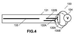
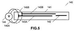
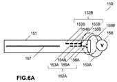
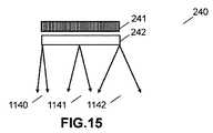
いくつかの実施形態によると、導波管デバイスは、少なくとも1つの光学基板と、少なくとも1つの光源と、源からの光を光学基板の中に結合するための少なくとも1つの光結合器と、光学基板からの光を抽出し、出力照明を形成するための少なくとも1つの光抽出器とを含む。図1Aに描写されるのは、導波管デバイスの実施形態である。故に、導波管デバイス(100)は、少なくとも1つの光学基板(101)と、少なくとも1つの入力格子(102)と、少なくとも1つの出力格子(103)とを含む。最大開口Wを有する、入力格子(102)は、源(104)からの光(光線矢印1000−1002)を導波管基板(101)内の全内部反射(TIR)経路(1004)の中に結合する。入力(102)および出力(103)格子は、図1Aに描写されるように、本明細書に説明される格子構成等の任意の適切な構成において存在してもよい。 According to some embodiments, the waveguide device comprises at least one optical substrate, at least one light source, at least one optical coupler for coupling light from the source into the optical substrate, and an optical device. And at least one light extractor for extracting light from the substrate and forming output illumination. Depicted in FIG. 1A is an embodiment of a waveguide device. The waveguide device (100) thus comprises at least one optical substrate (101), at least one input grating (102) and at least one output grating (103). The input grating (102), which has a maximum aperture W, directs light from the source (104) (ray arrows 1000-1002) into a total internal reflection (TIR) path (1004) in the waveguide substrate (101). Join. The input (102) and output (103) grids may be present in any suitable configuration, such as the grid configurations described herein, as depicted in FIG. 1A.
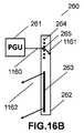
いくつかの実施形態では、導波管デバイスは、入力画像生成器を含み、これはさらに、光源と、マイクロディスプレイパネルと、光をコリメートするための光学とを有する、入力画像生成器を含む。いくつかの実施形態の説明では、入力生成器は、写真生成ユニット(PGU)と称される。いくつかの実施形態では、源は、画像情報に伴って変調されない、一般的照明を提供するように構成されてもよい。多くの実施形態では、入力画像生成器は、各ディスプレイピクセルが基板導波管内の一意の角度方向に変換されるように、マイクロディスプレイパネル上に表示される画像を投影する。種々の実施形態では、コリメーション光学は、少なくともレンズと、ミラーとを含む。多くの実施形態では、レンズおよびミラーは、回折性である。いくつかの実施形態では、光源は、少なくとも1つのレーザである。多数の実施形態では、光源は、少なくとも1つのLEDである。多くの実施形態では、異なる光源の種々の組み合わせが、入力画像生成器と併用される。 In some embodiments, the waveguide device includes an input image generator, which further includes an input image generator having a light source, a microdisplay panel, and optics for collimating light. In the description of some embodiments, the input generator is referred to as a photo generation unit (PGU). In some embodiments, the source may be configured to provide general illumination that is not modulated with the image information. In many embodiments, the input image generator projects the image displayed on the micro display panel such that each display pixel is translated into a unique angular orientation within the substrate waveguide. In various embodiments, collimation optics includes at least a lens and a mirror. In many embodiments, the lenses and mirrors are diffractive. In some embodiments, the light source is at least one laser. In many embodiments, the light source is at least one LED. In many embodiments, various combinations of different light sources are used with the input image generator.
いくつかの入力画像生成器は、例えば、米国特許出願第13/869,866号「HOLOGRAPHIC WIDE ANGLE DISPLAY」および米国特許出願第13/844,456号「TRANSPARENT WAVEGUIDE DISPLAY」に説明されるもの等の本発明の種々の実施形態に従って使用されてもよいことを理解されたい。多くの実施形態では、入力画像生成器は、光をマイクロディスプレイ上に指向させ、反射光を導波管に向かって透過させる、ビームスプリッタを含む。いくつかの実施形態では、ビームスプリッタは、ホログラフィックポリマー分散液晶(HPDLC)内に記録される格子である。多数の実施形態では、ビームスプリッタは、偏光ビームスプリッタ立方体である。いくつかの実施形態では、入力画像生成器は、スペックル除去器を組み込む。任意の適切なスペックル除去器が、例えば、米国特許第US8、565,560号「LASER ILLUMINATION DEVICE」に説明されるもの等の種々の実施形態において使用されることができる。 Some input image generators are, for example, those described in US patent application Ser. No. 13 / 869,866 “HOLOGRAPHIC WIDE ANGLE DISPLAY” and US patent application Ser. No. 13 / 844,456 “TRANSPARENT WAVEGUIDE DISPLAY”. It should be appreciated that it may be used in accordance with various embodiments of the invention. In many embodiments, the input image generator includes a beam splitter that directs light onto the microdisplay and transmits reflected light toward the waveguide. In some embodiments, the beam splitter is a grating recorded in a holographic polymer dispersed liquid crystal (HPDLC). In many embodiments, the beamsplitter is a polarizing beamsplitter cube. In some embodiments, the input image generator incorporates a speckle remover. Any suitable speckle remover can be used in various embodiments such as, for example, those described in US Pat. No. 8,565,560 "LASER ILLUMINATION DEVICE".
いくつかの実施形態では、光源はさらに、照明ビームの角度特性を修正するための1つ以上のレンズを組み込む。多くの実施形態では、画像源は、マイクロディスプレイまたはレーザベースのディスプレイである。光源のいくつかの実施形態は、LEDを利用し、これは、レーザより良好な均一性を提供し得る。レーザ照明が、使用される場合、照明バンディング効果のリスクは、より高いが、依然として、本明細書に説明されるような種々の実施形態に従って、排除または軽減され得る。多数の実施形態では、光源からの光は、偏光される。複数の実施形態では、画像源は、液晶ディスプレイ(LCD)マイクロディスプレイまたはシリコン上液晶(LCoS)マイクロディスプレイである。 In some embodiments, the light source further incorporates one or more lenses to modify the angular characteristics of the illumination beam. In many embodiments, the image source is a microdisplay or a laser based display. Some embodiments of the light source utilize LEDs, which may provide better uniformity than lasers. If laser lighting is used, the risk of lighting banding effects is higher, but still may be eliminated or mitigated according to various embodiments as described herein. In many embodiments, the light from the light source is polarized. In embodiments, the image source is a liquid crystal display (LCD) microdisplay or a liquid crystal on silicon (LCoS) microdisplay.
いくつかの実施形態では、入力画像生成器光学は、偏光ビームスプリッタ立方体を含む。多くの実施形態では、入力画像生成器光学は、ビームスプリッタコーティングが塗布されている、傾角プレートを含む。いくつかの実施形態では、入力画像生成器光学は、切替可能なブラッグ格子(SBG)を組み込み、これは、偏光選択的ビームスプリッタとして作用する。SBGを組み込む、入力画像生成器光学の実施例は、米国特許出願第13/869,866号「HOLOGRAPHIC WIDE ANGLE DISPLAY」および米国特許出願第13/844,456号「TRANSPARENT WAVEGUIDE DISPLAY」に開示される。多くの実施形態では、入力画像生成器光学は、照明光の開口数を制御するために、屈折コンポーネントおよび湾曲反射表面または回折光学要素のうちの少なくとも1つを含む。複数の実施形態では、入力画像生成器は、照明光の波長特性を制御するために、スペクトルフィルタを含む。いくつかの実施形態では、入力画像生成器光学は、迷光を制御するために、開口と、マスクと、フィルタと、コーティングとを含む。いくつかの実施形態では、マイクロディスプレイは、水盤光学を組み込む。 In some embodiments, the input image generator optics comprises a polarizing beamsplitter cube. In many embodiments, the input image generator optics includes a tilt plate, to which a beamsplitter coating is applied. In some embodiments, the input image generator optics incorporates a switchable Bragg grating (SBG), which acts as a polarization selective beamsplitter. Examples of input image generator optics incorporating SBGs are disclosed in US patent application Ser. No. 13 / 869,866 “HOLOGRAPHIC WIDE ANGLE DISPLAY” and US patent application Ser. No. 13 / 844,456 “TRANSPARENT WAVEGUIDE DISPLAY”. . In many embodiments, the input image generator optics includes at least one of a refractive component and a curved reflective surface or diffractive optical element to control the numerical aperture of the illumination light. In embodiments, the input image generator includes a spectral filter to control the wavelength characteristics of the illumination light. In some embodiments, the input imager optics includes apertures, masks, filters, and coatings to control stray light. In some embodiments, the microdisplay incorporates basin optics.
図1Aに描写される実施形態に戻ると、外部源(102)は、角度帯域幅(1002)内のコリメートされた光線を提供する。TIR経路(1004)内の光は、出力格子(103)と相互作用し、TIR光が格子による回折のための条件を満たす度に、光の一部を抽出する。ブラッグ格子の場合、抽出は、ブラッグ条件が満たされるときに生じる。例えば、TIR角度Uに対応する、光TIR光線経路(1004)は、出力格子によって出力方向(1005A)の中に回折される。基本幾何学的光学から、一意のTIR角度が各光入射角によって入力格子において画定されることが明白であるはずである。光が、抽出され、描写されるように、3つの抽出ビームを形成し、これはそれぞれ、2つの光線(1005Bおよび1005C;1006Aおよび1006B;1007Aおよび1007B)によって並置されるように描写される。完璧にコリメートされた間隙(平行線模様として描写される1006Cおよび1007C)が、隣接するビーム抽出間に存在し、バンディング効果をもたらすであろう。いくつかの実施形態によると、バンディングを生じさせるビーム間隙は、本明細書に説明されるように、いくつかのバンディング除去光学によって排除または最小限にされる。例えば、バンディング除去光学は、入力格子がTIR角度Uに依存する有効入力開口W’を有するように、光を構成する。 Returning to the embodiment depicted in FIG. 1A, the external source (102) provides collimated rays within the angular bandwidth (1002). The light in the TIR path (1004) interacts with the output grating (103) and extracts a portion of the light each time the TIR light meets the conditions for diffraction by the grating. In the case of the Bragg lattice, the extraction occurs when the Bragg condition is met. For example, the optical TIR ray path (1004), corresponding to the TIR angle U, is diffracted by the output grating into the output direction (1005A). From basic geometric optics, it should be clear that a unique TIR angle is defined at the input grating by each light incident angle. The light is extracted and forms three extraction beams as depicted, which are depicted as juxtaposed by two rays (1005B and 1005C; 1006A and 1006B; 1007A and 1007B), respectively. Perfectly collimated gaps (1006C and 1007C, depicted as parallel line patterns) will exist between adjacent beam extractions, resulting in banding effects. According to some embodiments, beam gaps that cause banding are eliminated or minimized by some banding removal optics, as described herein. For example, debanding optics configure the light such that the input grating has an effective input aperture W'that depends on the TIR angle U.
多数の実施形態では、導波管デバイスは、入力格子が、TIR角度の関数である、有効入力開口を有するように、瞳を偏移させ、導波管の中に結合される光を構成することが可能なバンディング除去光学を組み込む。バンディング除去光学の効果は、出力格子による導波管からの連続光抽出が、入力格子における任意の光入射角のための略平坦照明プロファイルを提供するように統合することである。いくつかの実施形態では、バンディング除去光学は、(限定ではないが)格子、部分的反射フィルム、液晶整合層、等方性屈折層、および勾配屈折率(GRIN)構造を含む、種々のタイプの光学ビーム修正層を組み合わせることによって実装される。用語「ビーム修正」は、入射光角度の関数としての3D空間内の振幅、偏光、位相、および波面変位の変動を指すことを理解されたい。それぞれの場合において、ビーム修正層は、いくつかの実施形態によると、入力格子における任意の光入射角のための出力格子を横断して均一抽出を与える、有効開口を提供する。多くの実施形態では、ビーム修正層は、入力角度の関数として入力光の開口数を制御するための手段と併用される。いくつかの実施形態では、ビーム修正層は、波長多様性を提供するための技法と併用される。 In many embodiments, the waveguide device shifts the pupil so that the input grating has an effective input aperture that is a function of the TIR angle and constitutes the light that is coupled into the waveguide. Incorporates a possible banding removal optics. The effect of debanding optics is to integrate continuous light extraction from the waveguide by the output grating to provide a substantially flat illumination profile for any light incident angle at the input grating. In some embodiments, debanding optics are of various types, including (but not limited to) gratings, partially reflective films, liquid crystal matching layers, isotropic refractive layers, and gradient index (GRIN) structures. It is implemented by combining optical beam modifying layers. It is to be understood that the term “beam modification” refers to variations in amplitude, polarization, phase, and wavefront displacement in 3D space as a function of incident light angle. In each case, the beam modifying layer, according to some embodiments, provides an effective aperture that provides uniform extraction across the output grating for any light incident angle on the input grating. In many embodiments, the beam modifying layer is used with a means for controlling the numerical aperture of the input light as a function of input angle. In some embodiments, the beam modifying layer is combined with techniques to provide wavelength diversity.
図1Bは、導波管からZとして標識される主伝搬方向(図1Aに示される座標系参照)に沿った光出力に及ぼす光学を偏移させる瞳の効果(Iとして標識される)を図示する、チャートを提供する。入力光方向に対応する3つの連続抽出に関する強度プロファイル(1008A−1008C)が、示される。強度プロファイルの形状は、ビーム修正層の規定によって制御される。いくつかの実施形態では、強度プロファイルは、略平坦強度プロファイルを提供するように統合される。例えば、強度プロファイル(1008A−1008C)は、平坦プロファイル(1009)の中に統合される。
導波管デバイスにおいて利用される入力結合器および抽出器FIG. 1B illustrates the effect of the optic-shifting pupil (labeled I) on the light output along the main propagation direction (see the coordinate system shown in FIG. 1A) labeled Z from the waveguide. Yes, provide a chart. Intensity profiles (1008A-1008C) for three consecutive extractions corresponding to the input light direction are shown. The shape of the intensity profile is controlled by the definition of the beam modifying layer. In some embodiments, the intensity profiles are combined to provide a generally flat intensity profile. For example, the intensity profile (1008A-1008C) is integrated into the flat profile (1009).
Input couplers and extractors used in waveguide devices
導波管デバイスは、現在、ある範囲のディスプレイおよびセンサ用途において着目されている。デバイスに関する早期の研究の多くは、反射ホログラムを対象としていたが、透過性デバイスが、光学システム構築ブロックとしてはるかに多用途であることが証明されている。故に、いくつかの実施形態は、瞳の入力または出力のために使用され得る、導波管デバイス内の格子の使用を対象とする。多くの実施形態では、入力格子は、源からの光を導波管の中に結合するための光の入力結合器のタイプである。多数の実施形態では、出力格子は、導波管からの光を抽出し、出力照明を形成するための光の光抽出器のタイプである。いくつかの実施形態では、導波管デバイスは、ブラッグ格子(体積格子とも称される)を利用する。ブラッグ格子は、わずかな光がより高次数に回折される、高効率を有する。回折およびゼロ次数における光の相対的量は、大瞳にわたって光を抽出するための有損失導波管格子を作製するために使用される性質である、格子の屈折率変調を制御することによって変動されることができる。 Waveguide devices are currently receiving attention in a range of display and sensor applications. Although much of the early work on devices focused on reflection holograms, transmissive devices have proven to be much more versatile as optical system building blocks. Thus, some embodiments are directed to the use of gratings in the waveguide device that may be used for pupil input or output. In many embodiments, the input grating is a type of optical input coupler for coupling light from the source into the waveguide. In many embodiments, the output grating is a type of light extractor for extracting light from the waveguide and forming output illumination. In some embodiments, the waveguide device utilizes a Bragg grating (also called a volume grating). Bragg gratings have high efficiency, where a small amount of light is diffracted into higher orders. The relative amount of light in diffraction and in the zero order is varied by controlling the index modulation of the grating, a property used to make lossy waveguide gratings for extracting light across a large pupil. Can be done.
本明細書で使用されるように、用語「格子」は、いくつかの実施形態では、格子のセットから成る格子を包含し得る。例えば、いくつかの実施形態では、入力格子および/または出力格子は、単一層の中に多重化された2つ以上の格子を別個に備える。ホログラフィの文献において、1つを上回るホログラフィック規定が単一ホログラフィック層の中に記録され得ることが、明確に認められている。そのような多重化されたホログラムを記録するための方法は、当業者に周知である。いくつかの実施形態では、入力格子および/または出力格子は、接触する、または1つ以上の薄い光学基板によって垂直に分離される、2つの重複格子層を別個に備える。多くの実施形態では、格子層は、並置ガラスまたはプラスチック基板間に挟み込まれる。いくつかの実施形態では、2つ以上の格子層は、スタックを形成し得、その中では、全内部反射が、外側基板および空気界面において生じる。いくつかの実施形態では、導波管デバイスは、単に、1つの格子層を備えてもよい。いくつかの実施形態では、電極が、基板の面に印加され、格子を回折状態とクリア状態との間で切り替える。スタックはさらに、多数の実施形態によると、ビーム分割コーティングおよび環境保護層等の付加的層を含む。 As used herein, the term "lattice" may, in some embodiments, encompass a lattice consisting of a set of lattices. For example, in some embodiments, the input and / or output gratings separately comprise two or more gratings multiplexed in a single layer. It is explicitly recognized in the holographic literature that more than one holographic definition can be recorded in a single holographic layer. Methods for recording such multiplexed holograms are well known to those skilled in the art. In some embodiments, the input and / or output gratings separately comprise two overlapping grating layers that are in contact or vertically separated by one or more thin optical substrates. In many embodiments, the lattice layers are sandwiched between juxtaposed glass or plastic substrates. In some embodiments, two or more lattice layers may form a stack in which total internal reflection occurs at the outer substrate and air interface. In some embodiments, the waveguide device may simply comprise one grating layer. In some embodiments, electrodes are applied to the surface of the substrate to switch the grating between a diffractive state and a clear state. The stack further includes additional layers, such as beam-splitting coatings and environmental protection layers, according to many embodiments.
多数の実施形態では、格子層は、別個の層に分割される。いくつかの層は、種々の実施形態によると、単一導波管基板の中にともに積層される。いくつかの実施形態では、格子層は、ともに積層され、単一基板導波管を形成する、入力結合器、折畳格子、および出力格子(またはその一部)を含む、いくつかの部品から作製される。多くの実施形態では、導波管デバイスの部品は、部品のものに合致する屈折率の光学糊または他の透明材料によって分離される。多数の実施形態では、格子層は、所望の格子厚さのセルを作成し、入力結合器、折畳格子、および出力格子毎に、各セルを切替可能なブラッグ格子(SBG)材料で真空充填することによって、セル作製プロセスを介して形成される。いくつかの実施形態では、セルは、入力結合器、折畳格子、および出力格子のための所望の格子厚を画定する、ガラスのプレート間の間隙を伴う、ガラスの複数のプレートを位置付けることによって形成される。多くの実施形態では、1つのセルが、別個の開口がSBG材料の異なるポケットで充填されるように、複数の開口とともに作製されてもよい。任意の介在空間は、種々の実施形態によると、分離材料(例えば、糊、油等)によって分離され、別個のエリアを画定する。複数の実施形態では、SBG材料は、基板上にスピンコーティングされ、次いで、材料の硬化後、第2の基板によって被覆される。折畳格子を使用することによって、導波管ディスプレイは、有利には、いくつかの実施形態による、情報を表示する以前のシステムおよび方法より少ない層を要求する。加えて、折畳格子を使用することによって、光は、二重瞳拡張を達成しながら、導波管内の全内部反射によって、導波管外側表面によって画定された単一長方形プリズム内を進行することができる。多くの実施形態では、入力結合器および格子は、基板内のある角度で光の2つの波に干渉し、ホログラフィック波面を作成し、それによって、所望の角度において導波管基板内に設定される明および暗フリンジを作成することによって作成されることができる。多数の実施形態では、所与の層内の格子は、記録レーザビームを格子エリアを横断して走査またはステップ処理することによって、ステップ毎方式において記録される。いくつかの実施形態では、格子は、ホログラフィック印刷産業において現在使用されているマスタおよび接触コピープロセスを使用して記録される。 In many embodiments, the lattice layer is divided into separate layers. Several layers are laminated together in a single waveguide substrate, according to various embodiments. In some embodiments, the grating layers are from several components that are laminated together to form a single substrate waveguide, including an input coupler, a folding grating, and an output grating (or a portion thereof). It is made. In many embodiments, the components of the waveguide device are separated by optical glue or other transparent material with an index of refraction that matches that of the components. In many embodiments, the lattice layer creates cells of a desired lattice thickness and vacuum fills each switch with a switchable Bragg grating (SBG) material for each input coupler, folding grid, and output grid. Is formed through the cell manufacturing process. In some embodiments, the cell is by positioning multiple plates of glass with a gap between the plates of glass defining the desired grating thickness for the input coupler, the folding grid, and the output grid. It is formed. In many embodiments, one cell may be made with multiple openings such that the separate openings are filled with different pockets of SBG material. Any intervening spaces are separated by a separating material (eg, glue, oil, etc.) to define separate areas, according to various embodiments. In embodiments, the SBG material is spin coated onto the substrate and then covered by the second substrate after the material has cured. By using a folded grating, the waveguide display advantageously requires fewer layers than previous systems and methods for displaying information, according to some embodiments. In addition, by using a folded grating, light travels within a single rectangular prism defined by the waveguide outer surface by total internal reflection within the waveguide while achieving double pupil expansion. be able to. In many embodiments, the input coupler and grating interfere with two waves of light at an angle within the substrate to create a holographic wavefront, thereby setting it in the waveguide substrate at the desired angle. Can be created by creating light and dark fringes. In many embodiments, the grating in a given layer is recorded in a step-by-step manner by scanning or stepping a recording laser beam across the grating area. In some embodiments, the grid is recorded using the master and contact copy processes currently used in the holographic printing industry.
入力および出力格子は、多くの実施形態によると、共通表面格子ピッチを有するように設計される。いくつかの実施形態では、入力格子は、各格子が入射非偏光の偏光を導波管経路の中に回折するように配向される、複数の格子を組み合わせる。多くの実施形態では、出力格子は、導波管経路からの光が、組み合わせられ、非偏光として、導波管から外に結合されるように配向される、複数の格子を組み合わせる。各格子は、3D空間内の少なくとも1つの格子ベクトル(またはKベクトル)によって特徴付けられ、これは、ブラッグ格子の場合、ブラッグフリンジに対して法線のベクトルとして画定される。格子ベクトルは、入力および回折される角度の所与の範囲にわたる光学効率を決定する。 The input and output grids, according to many embodiments, are designed to have a common surface grid pitch. In some embodiments, the input grating combines a plurality of gratings, each grating oriented to diffract incident unpolarized polarization into the waveguide path. In many embodiments, the output grating combines multiple gratings in which the light from the waveguide paths is oriented to be combined and uncoupled out of the waveguide as unpolarized light. Each grid is characterized by at least one grid vector (or K vector) in 3D space, which in the case of a Bragg grid is defined as a vector normal to the Bragg fringe. The grating vector determines the optical efficiency over a given range of input and diffracted angles.
格子の1つの重要なクラスは、切替可能なブラッグ格子(SBG)として知られ、これは、多くの実施形態によると、種々の導波管デバイスにおいて利用される。典型的には、ホログラフィックポリマー分散液晶(HPDLC)が、SBG内で使用される。多くの実施形態では、HPDLCは、混合液晶(LC)、モノマー、光開始剤染料、および共開始剤を含む。多くの場合、混合物はまた、界面活性剤を含む。特許および科学文献は、SBGを加工するために使用され得る、材料系およびプロセスの多くの実施例を含む。2つの基本特許は、Sutherlによる米国特許第5,942,157号およびTanaka et al.による米国特許第5,751,452号である。両申請は、SBGデバイスを加工するために好適なモノマーおよび液晶材料組み合わせを説明する。透過性SBGの公知の属性のうちの1つは、LC分子が格子フリンジ平面に対して法線に整合する傾向にあることである。LC分子整合の効果は、透過性SBGが、P偏光(すなわち、入射平面に偏光ベクトルを伴う光)を効率的に回折するが、S偏光(すなわち、入射平面に対して法線の偏光ベクトルを伴う光)に関して約ゼロ回折効率を有することである。透過性SBGは、入射と反射光との間の内包角が小さいとき、P偏光に関する任意の格子の回折効率がゼロになるため、グレージング角付近入射では使用されなくてもよい。 One important class of gratings is known as switchable Bragg gratings (SBGs), which, according to many embodiments, are utilized in various waveguide devices. Holographic polymer dispersed liquid crystals (HPDLC) are typically used within SBGs. In many embodiments, HPDLCs include mixed liquid crystals (LCs), monomers, photoinitiator dyes, and coinitiators. Often, the mixture also contains a surfactant. The patent and scientific literature includes many examples of material systems and processes that can be used to process SBGs. Two basic patents are US Pat. No. 5,942,157 by Suther and Tanaka et al. U.S. Pat. No. 5,751,452. Both applications describe suitable monomer and liquid crystal material combinations for processing SBG devices. One of the known attributes of transparent SBGs is that LC molecules tend to align normal to the lattice fringe plane. The effect of LC molecular matching is that the transmissive SBG efficiently diffracts P-polarized light (ie, light with a polarization vector in the plane of incidence), but S-polarized light (ie, a polarization vector normal to the plane of incidence). It has a diffraction efficiency of about zero. The transmissive SBG may not be used for near grazing angle incidence because the diffraction efficiency of any grating for P-polarized light is zero when the included angle between incident and reflected light is small.
いくつかの実施形態では、SBGは、最初に、光重合性モノマーと液晶材料の混合物の薄膜を平行ガラスプレート間に設置することによって加工される。一方または両方のガラスプレートは、電場をフィルムを横断して印加するための電極を支持する。多数の実施形態では、電極は、少なくとも部分的に、透明酸化インジウムスズフィルムによって作製される。体積位相格子が、複数の実施形態によると、次いで、傾けられたフリンジ格子構造を形成することに干渉する、2つの相互にコヒーレントなレーザビームで、液晶材料(多くの場合、シロップと称される)を照明することによって記録されることができる。記録プロセスの間、モノマーは、重合化し、混合物は、位相分離を受け、クリアポリマーの領域で介在された液晶微小液滴によって稠密に取り込まれる領域を作成し、HPDLCをもたらす。いくつかの実施形態によると、HPDLCデバイスの交互液晶豊富領域と液晶欠乏領域は、格子のフリンジ平面を形成する。結果として生じる体積位相格子は、非常に高回折効率を呈することができ、種々の実施形態によると、フィルムを横断して印加される電場の大きさによって制御され得る。電場が、透明電極を介して、格子に印加されると、LC液滴の自然配向は、変化され、フリンジの屈折率変調を低減させ、ホログラム回折効率を非常に低レベルまで降下させる。典型的には、SBG要素は、30μs以内でクリアに切り替えられ、オンに切り替えるために、より長い緩和時間を伴う。デバイスの回折効率は、多くの実施形態によると、連続範囲にわたって電圧を印加することによって調節されることができることに留意されたい。デバイスは、電圧が印加されないと、約100%効率を呈し、十分に高電圧が印加されると、約ゼロ効率を呈する。HPDLCデバイスのある実施形態では、磁場が、LC配向を制御するために使用されてもよい。HPDLCデバイスのある実施形態では、ポリマーからのLC材料の位相分離は、判別可能液滴構造が生じない程度まで遂行され得る。いくつかの実施形態では、SBGはまた、受動格子として使用され、これは、一意に高屈折率変調の利点を提供し得る。 In some embodiments, SBGs are processed by first placing a thin film of a mixture of photopolymerizable monomer and liquid crystal material between parallel glass plates. One or both glass plates carry electrodes for applying an electric field across the film. In many embodiments, the electrodes are made, at least in part, by a transparent indium tin oxide film. A liquid crystal material (often referred to as a syrup) with two mutually coherent laser beams that a volume phase grating interferes with forming a tilted fringe grating structure, according to embodiments. ) Can be recorded by illuminating. During the recording process, the monomers polymerize and the mixture undergoes phase separation, creating areas that are densely entrapped by the liquid crystal microdroplets mediated by areas of clear polymer, resulting in HPDLC. According to some embodiments, the alternating liquid crystal rich and liquid crystal depleted regions of the HPDLC device form the fringe plane of the lattice. The resulting volume phase grating can exhibit very high diffraction efficiency and, according to various embodiments, can be controlled by the magnitude of the electric field applied across the film. When an electric field is applied to the grating via the transparent electrode, the natural orientation of the LC droplets is changed, reducing the index modulation of the fringes and reducing the hologram diffraction efficiency to very low levels. Typically, SBG elements are switched clear within 30 μs, with a longer relaxation time to switch on. It should be noted that the diffraction efficiency of the device can be adjusted by applying a voltage over a continuous range, according to many embodiments. The device exhibits approximately 100% efficiency when no voltage is applied and approximately zero efficiency when a sufficiently high voltage is applied. In certain embodiments of HPDLC devices, a magnetic field may be used to control the LC orientation. In certain embodiments of the HPDLC device, phase separation of the LC material from the polymer can be accomplished to the extent that no discernible droplet structure occurs. In some embodiments, SBGs are also used as passive gratings, which may uniquely provide the benefits of high index modulation.
多数の実施形態によると、SBGは、自由空間用途のために、透過または反射格子を提供するために使用される。SBGの種々の実施形態は、HPDLCが導波管コアまたは一時的に結合される層のいずれかを導波管に近接して形成する、導波管デバイスとして実装される。多くの実施形態では、HPDLCセルを形成するために使用される、平行ガラスプレートは、全内部反射(TIR)光誘導構造を提供する。光は、いくつかの実施形態によると、切替可能な格子が、TIR条件以外の角度で光を回折するとき、SBGから外に結合される。 According to many embodiments, SBGs are used to provide transmissive or reflective gratings for free space applications. Various embodiments of SBGs are implemented as waveguide devices in which the HPDLC forms either the waveguide core or layers that are temporarily coupled in close proximity to the waveguide. In many embodiments, the parallel glass plates used to form HPDLC cells provide total internal reflection (TIR) light guiding structures. The light is coupled out of the SBG when the switchable grating diffracts the light at angles other than the TIR condition, according to some embodiments.
SBGに基づく導波管デバイスの多くの実施形態では、格子は、透明基板によって挟み込まれる単一層内に形成される。いくつかの実施形態では、導波管は、単に、1つの格子層である。切替可能な格子を組み込む、種々の実施形態では、透明電極は、切替可能な格子を挟み込む基板層の対向表面に適用される。いくつかの実施形態では、セル基板は、ガラスから加工される。例示的ガラス基板は、標準的Corning Willowガラス基板(屈折率1.51)であって、これは、50ミクロンまでの厚さで利用可能である。いくつかの実施形態では、セル基板は、光学プラスチックである。 In many embodiments of SBG-based waveguide devices, the grating is formed in a single layer sandwiched by transparent substrates. In some embodiments, the waveguide is simply one grating layer. In various embodiments incorporating a switchable grid, transparent electrodes are applied to opposing surfaces of the substrate layers that sandwich the switchable grid. In some embodiments, the cell substrate is fabricated from glass. An exemplary glass substrate is a standard Corning Willow glass substrate (refractive index 1.51), which is available in thicknesses up to 50 microns. In some embodiments, the cell substrate is optical plastic.
ブラッグ格子はまた、他の材料内にも記録され得ることを理解されたい。いくつかの実施形態では、SBGは、液体ポリマー中に分散される固体液晶の基質を有する、POLICRYPSまたはPOLIPHEM等の均一変調材料内に記録される。複数の実施形態では、SBGは、非切替可能である(すなわち、受動的)。非切替可能なSBGは、その液晶成分に起因して高屈折率変調を提供することが可能な従来のホログラフィックフォトポリマー材料に優る利点を有し得る。例示的均一変調液晶−ポリマー材料系は、Caputo et alによる米国特許出願公開第US2007/0019152号およびStumpe et al.によるPCT出願第PCT/EP2005/006950号(両方とも、参照することによってその全体として本明細書に組み込まれる)に開示される。均一変調格子は、高屈折率変調(故に、高回折効率)および低散乱によって特徴付けられる。多くの実施形態では、少なくとも1つの格子は、表面レリーフ格子である。いくつかの実施形態では、少なくとも1つの格子は、薄い(またはRaman−Nath)ホログラムである。 It should be appreciated that Bragg gratings can also be recorded in other materials. In some embodiments, SBGs are recorded in a homogeneous modulating material, such as POLICRYPS or POLIPHEM, which has a solid liquid crystal matrix dispersed in a liquid polymer. In embodiments, SBGs are non-switchable (ie, passive). Non-switchable SBGs may have advantages over conventional holographic photopolymer materials that can provide high index modulation due to their liquid crystal components. Exemplary uniformly modulated liquid crystal-polymer material systems are described in US Patent Application Publication No. US 2007/0019152 by Caputo et al and Stumpe et al. PCT Application No. PCT / EP2005 / 006950, both of which are hereby incorporated by reference in their entirety. Uniform modulation gratings are characterized by high index modulation (hence high diffraction efficiency) and low scattering. In many embodiments, at least one grating is a surface relief grating. In some embodiments, at least one grating is a thin (or Raman-Nath) hologram.
複数の実施形態では、格子は、逆モードHPDLC材料内に記録される。逆モードHPDLCは、格子が、電場が印加されないとき、受動的であって、電場の存在下では、回折性となるという点で、従来のHPDLCと異なる。逆モードHPDLCは、PCT出願第PCT/GB2012/000680号「IMPROVEMENTS TO HOLOGRAPHIC POLYMER DISPERSED LIQUID CRYSTAL MATERIALS AND DEVICES」に開示されるレシピおよびプロセスのいずれかに基づいてもよい。格子は、種々の実施形態による、上記の材料系のいずれかに記録されてもよいが、受動(非切替可能な)モードで使用される。加工プロセスは、切替可能な格子のために使用されるものと同じであるが、電極コーティング段階は、省略される。LCポリマー材料系は、その高屈折率変調の観点から、非常に望ましい。いくつかの実施形態では、格子は、HPDLC内に記録されるが、切替可能ではない。 In embodiments, the grating is recorded in the inverse mode HPDLC material. Reverse mode HPDLC differs from conventional HPDLC in that the grating is passive when no electric field is applied and diffractive in the presence of the electric field. Reverse mode HPDLC may be based on any of the recipes and processes disclosed in PCT Application No. PCT / GB2012 / 000680, "IMPROVEMENTS TO HOLOGRAPHIC POLYMER DISPERSED LIQUID CRYSTAL MATERIALS AND DEVICES". The grating may be recorded in any of the above material systems, according to various embodiments, but is used in a passive (non-switchable) mode. The fabrication process is the same as that used for the switchable grid, but the electrode coating step is omitted. LC polymer material systems are highly desirable in terms of their high refractive index modulation. In some embodiments, the grid is recorded in HPDLC but is not switchable.
いくつかの実施形態では、格子は、出力のコリメーションを調節するために、屈折力をエンコードする。多くの実施形態では、出力画像は、無限遠にある。多数の実施形態では、出力画像は、アイボックスから数メートルの距離に形成されてもよい。 In some embodiments, the grating encodes optical power to adjust the collimation of the output. In many embodiments, the output image is at infinity. In many embodiments, the output image may be formed a few meters away from the eyebox.
いくつかの実施形態では、入力格子は、別のタイプの入力結合器によって置換されてもよい。特定の実施形態では、入力格子は、プリズムまたは反射表面と置換される。いくつかの実施形態では、入力結合器は、切替可能なまたは非切替可能なSBG格子等のホログラフィック格子であることができる。入力結合器は、ディスプレイ源からのコリメートされた光を受光し、光を第1の表面と第2の表面との間の全内部反射を介して導波管内を進行させるように構成される。 In some embodiments, the input grid may be replaced by another type of input combiner. In a particular embodiment, the input grating is replaced with a prism or reflective surface. In some embodiments, the input combiner can be a holographic grating, such as a switchable or non-switchable SBG grating. The input coupler is configured to receive the collimated light from the display source and propagate the light in the waveguide via total internal reflection between the first surface and the second surface.
ホログラフィの文献では、1つを上回るホログラフィック規定が、単一ホログラフィック層の中に記録され得ることが明確に認められている。そのような多重化されたホログラムを記録するための方法は、当業者に周知である。いくつかの実施形態では、入力または出力格子のうちの少なくとも1つは、2つ以上の角度回折規定を組み合わせ、角度帯域幅を拡張させる。多くの実施形態では、入力または出力格子のうちの少なくとも1つは、2つ以上のスペクトル回折規定を組み合わせ、スペクトル帯域幅を拡張させる。多数の実施形態では、カラー多重化格子が、2つ以上の原色を回折するために使用される。 It is explicitly recognized in the holographic literature that more than one holographic definition can be recorded in a single holographic layer. Methods for recording such multiplexed holograms are well known to those skilled in the art. In some embodiments, at least one of the input or output gratings combines two or more angular diffraction prescriptions to extend the angular bandwidth. In many embodiments, at least one of the input or output gratings combines two or more spectral diffraction prescriptions to extend the spectral bandwidth. In many embodiments, a color multiplexing grating is used to diffract more than one primary color.
多くの実施形態は、本明細書に説明されるように、モノクロで動作される。しかしながら、カラー導波管は、本発明の種々の実施形態によると、モノクロ導波管のスタックを含む。いくつかの実施形態では、導波管デバイスは、赤色、緑色、および青色導波管層を使用する。いくつかの実施形態では、導波管デバイスは、赤色および青色/緑色層を使用する。いくつかの実施形態では、格子は全て、受動的、すなわち、非切替可能である。複数の実施形態では、少なくとも1つの格子は、切替可能である。いくつかの実施形態では、各層内の入力格子は、切替可能であって、導波管層間の色クロストークを回避する。いくつかの実施形態では、色クロストークは、ダイクロイックフィルタを赤色と青色および青色と緑色導波管の入力格子領域間に配置することによって回避される。 Many embodiments operate in monochrome, as described herein. However, the color waveguide comprises a stack of monochrome waveguides, according to various embodiments of the invention. In some embodiments, the waveguide device uses red, green, and blue waveguide layers. In some embodiments, the waveguide device uses red and blue / green layers. In some embodiments, the grids are all passive, ie non-switchable. In embodiments, at least one grid is switchable. In some embodiments, the input grating in each layer is switchable to avoid color crosstalk between waveguide layers. In some embodiments, color crosstalk is avoided by placing dichroic filters between the input grating regions of the red and blue and blue and green waveguides.
いくつかの実施形態では、光は、波長帯域幅によって特徴付けられる。多くの実施形態では、導波管デバイスは、光の波長帯域幅を多様化することが可能である。種々の実施形態によると、ブラッグ格子は、本質的にスペクトル帯域幅限定デバイスであって、LEDおよびレーザ等の狭帯域源を用いて最も効率的に利用される。ブラッグ格子は、多くの実施形態によると、格子規定および入射光線角度がブラッグ式を満たすと、高効率を伴って、2つの異なる波長帯域を回折する。フルカラー導波管は、複数の実施形態によると、赤色、緑色、および青色回折導波管層等の別個の特定の波長層を利用する。1つの層が3つの原色のうちの2つを回折する、2層解決策が、多数の実施形態では、使用される。多くの実施形態では、ブラッグ格子の自然スペクトル帯域幅は、色クロストークを最小限にするために適正である。しかしながら、色クロストークのより厳密な制御に関して、導波管層間に統合され、典型的には、入力格子に重複する、ダイクロイックフィルタおよび狭帯域フィルタ等の付加的コンポーネントが、使用されてもよい。
バンディング除去光学In some embodiments, the light is characterized by a wavelength bandwidth. In many embodiments, the waveguide device is capable of diversifying the wavelength bandwidth of light. According to various embodiments, Bragg gratings are essentially spectral bandwidth limited devices and are most efficiently utilized with narrow band sources such as LEDs and lasers. Bragg gratings, according to many embodiments, diffract two different wavelength bands with high efficiency when the grating definition and incident ray angle satisfy the Bragg equation. Full-color waveguides utilize separate, specific wavelength layers, such as red, green, and blue diffractive waveguide layers, according to embodiments. A two-layer solution, where one layer diffracts two of the three primary colors, is used in many embodiments. In many embodiments, the natural spectral bandwidth of the Bragg grating is adequate to minimize color crosstalk. However, for more precise control of color crosstalk, additional components integrated between the waveguide layers and typically overlapping the input grating, such as dichroic filters and narrowband filters, may be used.
Banding removal optics
多数の実施形態では、バンディング除去光学は、光学基板が厚さDを有するとき、入力開口が、光学基板内のTIR角度Uを提供するように構成され、角度Uが、2D tan(U)によって計算されるような有効入力開口である。図2に提供されるのは、ゼロバンディングの条件が存在するように、導波管基板(111)と、TIR(1012)とを含む、導波管の形態におけるバンディング除去光学を組み込む、導波管デバイス(110)の実施形態である。多くの実施形態では、間隙がTIR光線経路に沿った連続光抽出間に存在しない、ゼロバンディングの条件は、TIR角度Uおよび導波管基板厚Dのための有効入力開口が2D tan(U)によって与えられるときに生じる。 In many embodiments, the debanding optics is configured such that when the optical substrate has a thickness D, the input aperture is configured to provide a TIR angle U within the optical substrate, the angle U being 2D tan (U). The effective input aperture as calculated. Provided in FIG. 2 is a waveguide that incorporates debanding optics in the form of a waveguide, including a waveguide substrate (111) and a TIR (1012) such that a zero banding condition exists. 3 is an embodiment of a tube device (110). In many embodiments, the condition of zero banding, where no gap exists between successive light extractions along the TIR ray path, is that the effective input aperture for TIR angle U and waveguide substrate thickness D is 2D tan (U). Occurs when given by.
いくつかの実施形態では、バンディング除去光学は、回折効率、光学透過、偏光、または複屈折の少なくとも1つのTIR経路に沿って、光の空間変動を提供する。典型的空間変動(120)は、曲線(1020)によって、図3のチャートに提供され、Y−軸は、上記のパラメータのいずれかの値(例えば、回折効率)を指し、X−軸は、導波管内のビーム伝搬方向である。いくつかの実施形態では、空間変動は、2次元(導波管の平面)においてである。 In some embodiments, debanding optics provide spatial variation of light along at least one TIR path of diffraction efficiency, optical transmission, polarization, or birefringence. A typical spatial variation (120) is provided in the chart of FIG. 3 by curve (1020), where the Y-axis refers to the value of any of the above parameters (eg, diffraction efficiency) and the X-axis is The direction of beam propagation in the waveguide. In some embodiments, the spatial variation is in two dimensions (plane of the waveguide).
いくつかの実施形態では、バンディング除去光学は、各格子が、小瞳偏移を提供し、バンディングを排除または軽減させるように、複数の格子を有するように構成される、少なくとも1つの格子である。多くの実施形態では、複数の格子のスタックは、スタック内の格子間の分離が角度毎に瞳偏移を提供するように設計されるとき、小瞳偏移を達成する。いくつかの実施形態では、瞳偏移が可能な格子は、透明基板によって分離される。いくつかの実施形態では、瞳偏移が可能な格子は、受動的である。代替として、いくつかの実施形態では、格子は、電圧が印加されると、オンに切り替えられる。いくつかの実施形態では、側方相対的変位を有するように配列される、複数の格子は、瞳偏移を提供する。多数の実施形態では、複数の格子は、2次元アレイに構成され、格子要素の異なるサブアレイが、入射角に従って、その回折状態に切り替えられる。いくつかの実施形態では、格子は、アレイのスタックとして構成される。種々の実施形態では、別個の格子が、異なる波長帯域のために提供される。いくつかの実施形態では、格子は、多重化される。 In some embodiments, the debanding optics is at least one grating, each grating configured to have a plurality of gratings to provide a pupillary shift and eliminate or mitigate banding. . In many embodiments, a stack of multiple gratings achieves a small pupil shift when the separation between the gratings in the stack is designed to provide a pupil shift for each angle. In some embodiments, the pupil shiftable gratings are separated by a transparent substrate. In some embodiments, the pupil-shiftable grating is passive. Alternatively, in some embodiments the grid is switched on when a voltage is applied. In some embodiments, the plurality of gratings arranged to have a lateral relative displacement provides a pupil shift. In many embodiments, the gratings are arranged in a two-dimensional array, with different sub-arrays of grating elements being switched to their diffractive state according to the angle of incidence. In some embodiments, the grid is configured as a stack of arrays. In various embodiments, separate gratings are provided for different wavelength bands. In some embodiments, the lattice is multiplexed.
多くの実施形態では、格子は、導波管の主平面を横断して変動する、格子パラメータを有する。いくつかの実施形態では、回折効率は、回折される光の量対ゼロ次数光として導波管を辿って透過される光の量を制御するように変動され、それによって、導波管から抽出された光の均一性が微調整されることを可能にする。いくつかの実施形態では、少なくとも1つの格子のKベクトルは、回転Kベクトルを有し、これは、導波管から抽出された光の均一性を微調整するように最適化された方向を有する。種々の実施形態では、格子の屈折率変調は、導波管から抽出された光の均一性を微調整するように変動される。多数の実施形態では、格子の厚さが、導波管から抽出された光の均一性を微調整するように変動される。 In many embodiments, the grating has grating parameters that vary across the major plane of the waveguide. In some embodiments, the diffraction efficiency is varied to control the amount of diffracted light versus the amount of light that is transmitted through the waveguide as zero-order light, thereby extracting from the waveguide. Allows the uniformity of the light provided to be fine-tuned. In some embodiments, the K vector of the at least one grating comprises a rotating K vector, which has a direction optimized to fine tune the homogeneity of the light extracted from the waveguide. .. In various embodiments, the index modulation of the grating is varied to fine tune the homogeneity of the light extracted from the waveguide. In many embodiments, the thickness of the grating is varied to fine tune the uniformity of the light extracted from the waveguide.
いくつかの実施形態では、バンディング除去光学は、電圧が印加されると、オンになり、瞳を偏移させ、バンディング効果を排除または軽減させる、スタックされた切替可能な格子として構成される、少なくとも1つの格子である。図4に描写されるのは、スタックされた切替可能な入力格子(132Aおよび132B)と、非切替可能な出力格子(133)とを有する、光学基板(131)を伴う、導波管デバイス(130)の実施形態である。電圧源(134)が、電気接続(135Aおよび135B)によって、入力格子(132Aおよび132B)に結合され、入力格子(132Aおよび132B)をオンに切り替え、瞳偏移を提供する。図5に描写されるのは、スタックされた格子層(143Aおよび143B)を有する、非切替可能な入力格子および切替可能な出力格子を有する、導波管デバイス(141)の実施形態である。電圧源(144)は、電気接続(145Aおよび145B)によって、出力格子(143Aおよび143B)に結合され、出力格子(143Aおよび143B)をオンに切り替え、瞳偏移を提供する。種々の実施形態では、薄い基板層が、スタックされた格子間に存在し、少なくとも一部の分離を提供する。 In some embodiments, the debanding optics are configured as stacked switchable gratings that are turned on when a voltage is applied to shift the pupil and eliminate or mitigate banding effects, at least. It is one grid. Depicted in FIG. 4 is a waveguide device (with optical substrate (131) with stacked switchable input gratings (132A and 132B) and non-switchable output grating (133). 130). A voltage source (134) is coupled to the input grids (132A and 132B) by electrical connections (135A and 135B) to turn on the input grids (132A and 132B) and provide pupil shift. Depicted in FIG. 5 is an embodiment of a waveguide device (141) having a non-switchable input grating and a switchable output grating with stacked grating layers (143A and 143B). The voltage source (144) is coupled to the output grids (143A and 143B) by electrical connections (145A and 145B) to turn on the output grids (143A and 143B) and provide pupil shift. In various embodiments, thin substrate layers are present between the stacked lattices to provide at least some isolation.
いくつかの実施形態では、バンディング除去光学は、電圧が印加されると、特定の要素をオンにし、瞳を偏移させ、バンディング効果を排除または軽減させる、切替可能な格子要素のアレイとして構成される、少なくとも1つの格子である。図6Aに描写されるのは、それぞれ、複数の格子要素(153A−156Aおよび153B−156B)を有する、入力格子(152Aおよび152B)と、出力格子(157)とを含む、光学基板(151)を有する、導波管デバイス(150)の実施形態である。導波管デバイスはさらに、個々に、各要素(例えば、156Aおよび156B)をオンに切り替え、瞳を偏移させるように構成される、電気接続(159Aおよび159B)によって各入力格子(152Aおよび152B)に結合される、電圧源(158)含む。描写されないが、電圧源は、要素毎に接続され、切替可能な要素のアレイを作成することができることを理解されたい。さらに、図6Aは、アレイであるように構成される、入力格子のみを描写するが、本発明のいくつかの実施形態によると、出力格子もまた、要素のアレイであることができ、各要素は、切替可能であるように構成されることを理解されたい。 In some embodiments, the debanding optics is configured as an array of switchable grating elements that, when energized, turns on certain elements, shifts the pupil, and eliminates or reduces banding effects. At least one grid. Depicted in FIG. 6A is an optical substrate (151) that includes an input grating (152A and 152B) and an output grating (157), each having a plurality of grating elements (153A-156A and 153B-156B). 3 is an embodiment of a waveguide device (150) having The waveguide device is further individually tuned to each input grating (152A and 152B) by electrical connections (159A and 159B) that are configured to turn on each element (eg, 156A and 156B) and shift the pupil. ), A voltage source (158). Although not depicted, it should be understood that the voltage sources can be connected element by element to create an array of switchable elements. Further, while FIG. 6A depicts only the input grid, which is configured to be an array, according to some embodiments of the invention the output grid may also be an array of elements, each element It is to be appreciated that is configured to be switchable.
種々の実施形態では、格子は、複数の回転Kベクトルを有する。K−ベクトルは、格子平面(またはフリンジ)に対して法線に整合されるベクトルであって、これは、入力および回折される角度の所与の範囲にわたる光学効率を決定する。回転Kベクトルは、いくつかの実施形態によると、導波管厚を増加させる必要なく、格子の角度帯域幅が拡張されることを可能にする。図6Bに描写されるのは、4つの回転Kベクトル(K1−K4)を有する、格子(152C)の実施形態である。いくつかの実施形態では、格子は、切替可能な要素の2次元アレイとして構成される。例えば、図7に描写されるように、格子は、切替可能な要素(例えば、161)の2次元アレイ(160)として構成される。In various embodiments, the grid has a plurality of rotated K-vectors. The K-vector is the vector that is aligned normal to the grating plane (or fringe), which determines the optical efficiency over a given range of input and diffracted angles. The rotating K-vector, according to some embodiments, allows the angular bandwidth of the grating to be extended without having to increase the waveguide thickness. Depicted in FIG. 6B is an embodiment of a lattice (152C) withfour rotated K vectors (K1 -K4 ). In some embodiments, the grid is configured as a two dimensional array of switchable elements. For example, as depicted in FIG. 7, the grid is configured as a two dimensional array (160) of switchable elements (eg, 161).
多数の実施形態では、バンディング除去光学は、瞳を偏移させ、バンディング効果を排除または軽減させるように構成される、複数の受動格子層であるように構成される、少なくとも1つの格子である。導波管デバイスが、複数の受動格子層を組み込むとき、種々の実施形態によると、基本アーキテクチャは、能動格子層(例えば、図4および5参照)を組み込むが、電圧源を伴わない、実施形態のうちのいくつかに類似する。いくつかの実施形態では、SBGを非切替可能なモードで使用し、いくつかの液晶ポリマー材料系によって与えられる、より高い屈折率変調を利用することが有利である。多くの実施形態では、バンディング除去光学は、瞳を偏移させ、バンディング効果を排除または軽減させるように構成される、少なくとも1つの多重化された格子である。 In many embodiments, the debanding optics is at least one grating configured to be a plurality of passive grating layers configured to shift the pupil and eliminate or mitigate banding effects. When the waveguide device incorporates multiple passive lattice layers, according to various embodiments, the basic architecture incorporates an active lattice layer (see, eg, FIGS. 4 and 5) but without a voltage source. Similar to some of the. In some embodiments, it is advantageous to use the SBG in a non-switchable mode to take advantage of the higher index modulation provided by some liquid crystal polymer material systems. In many embodiments, the debanding optics is at least one multiplexed grating configured to shift the pupil and eliminate or mitigate banding effects.
いくつかの実施形態では、導波管デバイスは、射出瞳拡張を提供するための折畳格子を含む。種々の折畳格子が、本発明の種々の実施形態によると、使用されてもよいことを理解されたい。多数の実施形態において使用され得る、種々の折畳格子の実施例は、PCT出願第PCT/GB2016000181号「WAVEGUIDE DISPLAY」に開示される、または本明細書に引用される他の参考文献に説明される。折畳格子は、いくつかの実施形態によると、瞳を偏移させ、バンディング効果を排除または軽減させるための複数の格子を組み込み、各格子は、小瞳偏移を提供する。 In some embodiments, the waveguide device includes a folded grating to provide exit pupil expansion. It should be appreciated that various folding grids may be used in accordance with various embodiments of the invention. Examples of various folded grids that may be used in numerous embodiments are disclosed in PCT application No. PCT / GB2016000181, "WAVEGUIDE DISPLAY," or described in other references cited herein. It Folded gratings, according to some embodiments, incorporate multiple gratings to shift the pupil and eliminate or mitigate banding effects, each grating providing a small pupil shift.
多くの実施形態では、バンディング除去光学は、1つ以上の屈折率層が、光線角度または光線位置のうちの少なくとも1つの関数として、光学基板内の光線経路に影響を及ぼし、瞳を偏移させ、バンディング効果を軽減させるように、光学基板内に配置される、1つ以上の屈折率層である。いくつかの実施形態では、少なくとも1つの屈折率層は、GRIN媒体である。米国仮特許出願第62/123,282号「NEAR EYE DISPLAY USING GRADIENT INDEX OPTICS」および米国仮特許出願第62/124,550号「WAVEGUIDE DISPLAY USING GRADIENT INDEX OPTICS」に説明される、種々のGRIN媒体の実施例等、種々のGRIN媒体が、本発明の種々の実施形態に従って使用されてもよいことを理解されたい。 In many embodiments, de-banding optics have one or more refractive index layers that affect the ray path in the optical substrate and shift the pupil as a function of at least one of ray angle or ray position. , One or more refractive index layers disposed within the optical substrate to reduce banding effects. In some embodiments, at least one index layer is a GRIN medium. U.S. Provisional Patent Application No. 62 / 123,282, "NEAR EYE DISPLAY USING GRADIENT INDEX OPTICS" and US Provisional Patent Application No. 62 / 124,550, "WAVEGUIDE DISPLAY USING GRADIENT INDEX OPTICS", various GRs of media. It should be appreciated that various GRIN media, such as the examples, may be used in accordance with various embodiments of the invention.
いくつかの実施形態では、バンディング除去光学は、1つ以上の層が、瞳偏移を提供し、バンディング効果を排除または軽減させるように構成されるように、光学基板の縁の少なくとも1つの反射表面に隣接して配置される、1つ以上の屈折率層である。図8に描写されるのは、入力格子(172)と、出力格子(173)とを含み、1つ以上のスタックされた屈折率層(174)が、1つ以上の屈折率層が瞳偏移を提供するように、導波管の上側反射表面に隣接して配置される、光学基板(171)を有する、導波管デバイス(170)の実施形態である。多くの実施形態では、バンディング除去光学は、1つ以上の層が、瞳偏移を提供し、バンディング効果を排除または軽減させるように構成される、光学基板内に配置される、1つ以上の屈折率層である。例えば、図9に描写されるのは、入力格子(182)と、出力格子(183)とを含み、1つ以上のスタックされた屈折率層(184)が、1つ以上の層(184)が瞳偏移を提供するように構成される、光学基板(181)内に配置される、光学基板(181)を有する、導波管デバイス(180)の実施形態である。いくつかの実施形態では、導波管デバイスは、光学基板内に配置される、1つ以上の屈折率層と、また、光学基板の少なくとも1つの反射表面に隣接して配置される、1つ以上の屈折率層とを含む、バンディング除去光学を組み込む。 In some embodiments, the debanding optics includes at least one reflection of an edge of an optical substrate such that one or more layers are configured to provide pupil shift and eliminate or mitigate banding effects. One or more refractive index layers disposed adjacent to the surface. Depicted in FIG. 8 is one that includes an input grating (172) and an output grating (173), one or more stacked index layers (174), one or more index layers being pupil-polarized. FIG. 7 is an embodiment of a waveguide device (170) having an optical substrate (171) positioned adjacent an upper reflective surface of the waveguide to provide transfer. In many embodiments, debanding optics include one or more layers disposed within an optical substrate in which one or more layers are configured to provide pupil shift and eliminate or mitigate banding effects. It is a refractive index layer. For example, depicted in FIG. 9 includes an input grating (182) and an output grating (183) with one or more stacked index layers (184) being one or more layers (184). Is an embodiment of a waveguide device (180) having an optical substrate (181) disposed within the optical substrate (181) configured to provide a pupil shift. In some embodiments, the waveguide device includes one or more refractive index layers disposed within the optical substrate and one disposed adjacent to at least one reflective surface of the optical substrate. Incorporating banding removal optics including the above refractive index layers.
いくつかの実施形態では、バンディング除去光学は、入力格子の前縁に対する光の光線束の一意の変位が、任意の所与の入射光方向のための入力格子によって提供され、瞳を偏移させ、バンディング効果を排除または軽減させるように、入射光に結合することが可能な前縁を有する、入力格子である。図10に描写されるのは、前縁(193)を伴う入力格子(192)を含む、光学基板(191)を有する、導波管デバイス(190)の実施形態の詳細である。2つの異なる入力角度(1090および1091)のためのコリメートされた入力光線経路および対応する回折された光線(1092および1093)が、描写される。入力格子(1094および1095)の前縁からの2つの光線セットの縁の分離も、描写される。いくつかの実施形態では、光線束の入力格子の縁に対する光の変位は、ビームの一部を入力格子開口の外側にもたらし、したがって、入射光の画角に応じて、光学基板の内側のTIR経路の中に回折されない。好適な吸収フィルムは、種々の実施形態によると、非回折光を捕捉する。故に、ビーム幅は、図2に関連してより詳細に説明されたように、TIR角度Uおよび導波管基板厚Dが2D tan(U)によって与えられるとき、バンディング除去条件を満たすように調整されることができる。そのような実施形態の実施例は、後続節により詳細に議論されるであろう(図20参照)。 In some embodiments, debanding optics provide a unique displacement of the bundle of rays of light with respect to the leading edge of the input grating, provided by the input grating for any given incident light direction, to shift the pupil. , An input grating having a leading edge that can be coupled to incident light so as to eliminate or reduce banding effects. Depicted in FIG. 10 are details of an embodiment of a waveguide device (190) having an optical substrate (191) that includes an input grating (192) with a leading edge (193). Collimated input ray paths and corresponding diffracted rays (1092 and 1093) for two different input angles (1090 and 1091) are depicted. The separation of the edges of the two ray sets from the leading edges of the input gratings (1094 and 1095) is also depicted. In some embodiments, the displacement of the light with respect to the edges of the input grating of the bundle of rays brings a portion of the beam outside the input grating aperture, thus depending on the angle of view of the incident light, the TIR inside the optical substrate. Not diffracted into the path. Suitable absorbing films, according to various embodiments, trap undiffracted light. Therefore, the beam width is adjusted to satisfy the banding removal condition when the TIR angle U and the waveguide substrate thickness D are given by 2D tan (U), as described in more detail in connection with FIG. Can be done. Examples of such embodiments will be discussed in more detail in subsequent sections (see Figure 20).
多くの実施形態では、バンディング除去光学は、入射光の複数のコリメートされた入射光線経路が、光線経路入力角度によって決定されるような異なるTIR光線経路の中に回折され、投影された瞳が、複数のコリメートされた入射光線経路毎に、光学基板内の一意の場所に形成され、バンディング効果を排除または軽減させることが可能であるように、回折効率の変動を有するように構成される、入力格子である。図11に描写されるのは、入力格子(202)を含む、光学基板(201)を有する、導波管デバイス(200)の実施形態の詳細である。2つの異なる入力角度(1100および1101)のためのコリメートされた入力光線経路は、回折された光線(1102および1103)がそれぞれ、光学基板(201)を辿ってTIR経路に追従するように、入力格子(202)によって回折される。各TIR光線経路(1104および1105)は、入射角に基づいて、バンディング効果が排除および/または軽減されるように、投影された瞳(1106および1107)を一意の場所に形成する。 In many embodiments, the banding optics diffracts multiple collimated incident ray paths of the incident light into different TIR ray paths as determined by the ray path input angle, and the projected pupil is An input, formed at each unique location within the optical substrate for each of a plurality of collimated incident ray paths, configured to have a variation in diffraction efficiency so that banding effects can be eliminated or mitigated. It is a grid. Depicted in FIG. 11 are details of an embodiment of a waveguide device (200) having an optical substrate (201) that includes an input grating (202). The collimated input ray paths for two different input angles (1100 and 1101) are input so that the diffracted rays (1102 and 1103) each follow the optical substrate (201) and follow the TIR path. Diffracted by the grating (202). Each TIR ray path (1104 and 1105) forms a projected pupil (1106 and 1107) at a unique location such that banding effects are eliminated and / or mitigated based on the angle of incidence.
いくつかの実施形態では、回折効率の変動は、主導波管方向に沿って変動し、少なくとも部分的に、瞳偏移を提供し、バンディング効果を排除または軽減させる。多くの実施形態では、回折効率の変動は、入力格子の開口にわたって2次元で変動する。 In some embodiments, the variation in diffraction efficiency varies along the main waveguide direction to provide, at least in part, pupil shift and eliminate or reduce banding effects. In many embodiments, the variation in diffraction efficiency varies in two dimensions across the aperture of the input grating.
いくつかの実施形態では、バンディング除去光学は、部分反射層が、入射光を透過光および反射光に分離し、瞳を偏移させ、バンディング効果を排除または軽減させるように、光学基板内に配置される、部分反射層である。図12に描写されるのは、入射光(1110)を透過光(1000)および反射光(1111)に分離することが可能な部分反射層(212)を含む、光学基板(211)を有する、導波管デバイス(210)の実施形態の詳細である。透過光および反射光(1000および1111)はそれぞれ、導波管基板(211)に沿ってTIR経路に追従し、瞳偏移をもたらし、バンディング効果を排除または軽減させる。 In some embodiments, de-banding optics are disposed within the optical substrate such that the partially reflective layer separates incident light into transmitted and reflected light, shifts the pupil, and eliminates or reduces banding effects. Is a partially reflective layer. Depicted in FIG. 12 has an optical substrate (211) that includes a partially reflective layer (212) capable of separating incident light (1110) into transmitted light (1000) and reflected light (1111), 3 is a detail of an embodiment of a waveguide device (210). The transmitted and reflected light (1000 and 1111), respectively, follow the TIR path along the waveguide substrate (211), causing a pupil shift and eliminating or mitigating banding effects.
多数の実施形態では、バンディング除去光学は、偏光修正層が、入射光を透過光および反射光に分離し、瞳を偏移させ、バンディング効果を排除または軽減させるように、光学基板内に配置される、偏光修正層である。例えば、図13は、偏光ベクトル(1123)を有する入射光(1120)を、偏光修正層(222)の遅延効果から生じる偏光ベクトル(1124)を有する、透過光(1121)と、反射光(1122)とに分離する、部分反射偏光修正層(222)を含む、光学基板(221)を有する、導波管デバイス(220)の実施形態の詳細を提供する。透過光(1121)および反射光(1122)は、光学基板(221)を辿ってTIR経路に追従し、瞳偏移をもたらし、バンディング効果を排除または軽減させる。いくつかの実施形態では、偏光修正層は、ポリマー材料を少なくとも1次元に延伸させることによって形成される。特定の実施形態では、偏光修正層は、複屈折ポリエステル、ポリメタクリル酸メチル(PMMA)、またはポリエチレンテレフタレート(PET)等のポリマー材料である。ポリマー材料は、単一層内で使用されてもよい、または2つ以上のものが、スタック内で組み合わせられてもよい。 In many embodiments, debanding optics are arranged in the optical substrate such that the polarization modifying layer separates incident light into transmitted and reflected light, shifts the pupil, and eliminates or reduces banding effects. It is a polarization correction layer. For example, FIG. 13 shows an incident light (1120) having a polarization vector (1123), a transmitted light (1121) and a reflected light (1122) having a polarization vector (1124) resulting from the delay effect of the polarization modifying layer (222). 2) provides details of an embodiment of a waveguide device (220) having an optical substrate (221) that includes a partially reflective polarization modifying layer (222). The transmitted light (1121) and reflected light (1122) follow the optical substrate (221) to follow the TIR path, resulting in pupil shift and eliminating or mitigating banding effects. In some embodiments, the polarization modifying layer is formed by stretching a polymeric material in at least one dimension. In certain embodiments, the polarization modifying layer is a polymeric material such as birefringent polyester, polymethylmethacrylate (PMMA), or polyethylene terephthalate (PET). The polymeric materials may be used in a single layer or two or more may be combined in a stack.
多くの実施形態では、バンディング除去光学は、任意の入射光角度のための抽出された光の非均一性を相殺し、バンディング効果を排除または軽減する、少なくとも2つの別個の導波管経路を提供するように構成される、少なくとも1つの格子である。いくつかの実施形態では、バンディング除去光学は、瞳偏移を提供し、バンディング効果を排除または軽減させるように構成される、少なくとも1つの折畳格子射出瞳エクスパンダと併用される、交差傾角格子を有する、少なくとも1つの格子を含む。図14に描写されるのは、入力画像生成器(232)に結合される光学基板(231)を有する、導波管デバイス(230)の実施形態である。光学基板(231)は、交差傾角格子(233Aおよび233B)を伴う入力格子(233)と、格子(235)を含む、第1の折畳格子射出瞳エクスパンダ(234)と、格子(237)を含む第2の折畳格子射出瞳エクスパンダ(236)と、交差傾角格子(238Aおよび238B)を伴う出力格子(238)とを含む。入力格子(233)は、方向が入力格子(233)の表面に対して法線であるような方向(1130)において、入力画像生成器(232)からの光を受光する。多数の実施形態では、格子内の交差格子は、光学基板の平面において、約90度の相対的角度を有する。しかしながら、実際は、他の角度も、使用されてもよく、依然として、本発明の種々の実施形態内であることに留意されたい。 In many embodiments, debanding optics provide at least two separate waveguide paths that offset the non-uniformity of the extracted light for any incident light angle and eliminate or mitigate banding effects. At least one grating configured to In some embodiments, the de-banding optics is used in combination with at least one folding grating exit pupil expander configured to provide pupil shift and eliminate or mitigate banding effects. With at least one grating. Depicted in FIG. 14 is an embodiment of a waveguide device (230) having an optical substrate (231) coupled to an input image generator (232). The optical substrate (231) includes an input grating (233) with crossed tilt gratings (233A and 233B), a first folding grating exit pupil expander (234) including a grating (235), and a grating (237). A second folded grid exit pupil expander (236) including an output grid (238) with cross-tilt grids (238A and 238B). The input grating (233) receives light from the input image generator (232) in a direction (1130) such that the direction is normal to the surface of the input grating (233). In many embodiments, the cross gratings within the grating have a relative angle in the plane of the optical substrate of about 90 degrees. However, it should be noted that in practice other angles may also be used and are still within the various embodiments of the invention.
いくつかの実施形態では、バンディング除去光学は、入力格子および出力格子がそれぞれ、直交偏光状態のためのピーク回折効率を伴う交差格子を組み合わせるような格子のシステムである。いくつかの実施形態では、入力および出力格子によって作成された偏光状態は、S−偏光およびP−偏光される。いくつかの実施形態では、入力および出力格子によって作成された偏光状態は、円偏光の反対向きである。いくつかの実施形態は、SBG等の液晶ポリマー系内に記録される格子を利用し、これは、その固有の複屈折および強力な偏光選択性を呈することに起因する利点を有し得る。しかしながら、一意の偏光状態を提供するように構成され得る、他の格子技術も、使用されてもよく、依然として、本発明の種々の実施形態内であることに留意されたい。 In some embodiments, debanding optics is a system of gratings such that the input and output gratings each combine a crossed grating with peak diffraction efficiency for orthogonal polarization states. In some embodiments, the polarization states created by the input and output gratings are S-polarized and P-polarized. In some embodiments, the polarization states created by the input and output gratings are in the opposite direction of circular polarization. Some embodiments utilize a grating recorded in a liquid crystal polymer system such as SBG, which may have advantages due to its inherent birefringence and exhibiting strong polarization selectivity. However, it should be noted that other grating techniques that may be configured to provide unique polarization states may also be used and are still within the various embodiments of the invention.
図14に戻ると、方向(1130)に沿って入力格子(233)上に入射する入力光の第1の偏光成分は、格子(233B)によってTIR経路の中に方向(1131)に沿って指向され、第2の偏光成分は、第2の格子(233A)によって第2のTIR経路の中に方向(1132)に沿って指向される。TIR経路(1131および1132)に沿って進行する光は、折畳格子(234および236)によって、光学基板(231)の平面内で拡張され、第2のTIR経路(1133および1134)の中に出力格子(238)に向かって回折される。出力格子(238)の交差傾角(238Aおよび238B)は、バンディング効果が排除または軽減されるように、第2のTIR経路(1133および1134)からの光を均一出力経路(1135)の中に回折する。いくつかの実施形態では、格子規定は、格子との誘導される光の二重相互作用を提供するように設計され、これは、折畳格子角度帯域幅を向上させ得る。米国特許出願第14/620,969号「WAVEGUIDE GRATING DEVICE」に説明される格子等の二重相互作用折畳格子のいくつかの実施形態が、使用されることができる。 Returning to FIG. 14, the first polarization component of the input light incident on the input grating (233) along the direction (1130) is directed by the grating (233B) into the TIR path along the direction (1131). And the second polarization component is directed by the second grating (233A) into the second TIR path along direction (1132). Light traveling along the TIR paths (1131 and 1132) is expanded in the plane of the optical substrate (231) by the folding gratings (234 and 236) into the second TIR paths (1133 and 1134). Diffracted towards the output grating (238). The cross tilt angles (238A and 238B) of the output grating (238) diffract the light from the second TIR path (1133 and 1134) into the uniform output path (1135) so that banding effects are eliminated or mitigated. To do. In some embodiments, the grating definition is designed to provide a double interaction of guided light with the grating, which may improve the folded grating angular bandwidth. Some embodiments of double-interacting folded lattices, such as the lattice described in US patent application Ser. No. 14 / 620,969 "WAVE GUIDE GRATING DEVICE", can be used.
いくつかの実施形態では、バンディング除去光学は、少なくとも1つの方向に沿って空間的に変動され、瞳を偏移させ、バンディング効果を排除または軽減させることが可能な可変有効開口数(NA)を提供する、マイクロディスプレイ内の光学コンポーネントである。図15に描写されるのは、マイクロディスプレイ(241)パネルの片側に高NAから、他側における低NAに平滑に変動し、瞳偏移を提供する、開口数(NA)変動を有するように設計される、入力画像生成器(240)の実施形態である。説明の目的のために、マイクロディスプレイに関連するNAは、本明細書では、マイクロディスプレイに対して法線の軸に対してマイクロディスプレイ表面上の点からの画像光線錐の最大角度の正弦に比例すると定義される。図15に示されるように、マイクロディスプレイ(241)のNAは、NAを、延在する光線(1140−1142)によって示されるように、マイクロディスプレイの少なくとも1つの主寸法を横断して変動させる、光学コンポーネント(242)によって空間的に変動される。NAを変動させるために使用される光学コンポーネントは、PCT出願第PCT/GB2016000181号「WAVEGUIDE DISPLAY」に説明される光学コンポーネントのいずれか等の任意の適切な光学コンポーネントであってもよいことを理解されたい。複数の実施形態では、微小電気機械システム(MEMS)アレイが、マイクロディスプレイディスプレイパネルを横断して(NA)を空間的に変動させるために使用される。多数の実施形態では、MEMアレイは、マイクロディスプレイパネルから反射された光のNAを空間的に変動させる。多くの実施形態では、MEMSアレイは、データプロジェクタ内で使用される技術を利用する。 In some embodiments, the debanding optics have a variable effective numerical aperture (NA) that can be spatially varied along at least one direction to shift the pupil and eliminate or mitigate banding effects. Provided are the optical components within the microdisplay. Depicted in FIG. 15 is to have a numerical aperture (NA) variation that smoothly varies from high NA on one side of the microdisplay (241) panel to low NA on the other side, providing pupil shift. 3 is an embodiment of an input image generator (240) designed. For purposes of explanation, the NA associated with a microdisplay is herein proportional to the sine of the maximum angle of the image ray cone from a point on the microdisplay surface with respect to the axis of the normal to the microdisplay. Then it is defined. As shown in FIG. 15, the NA of the microdisplay (241) causes the NA to vary across at least one major dimension of the microdisplay, as indicated by the extending rays (1140-1142), It is spatially varied by the optical component (242). It is understood that the optical component used to vary the NA may be any suitable optical component, such as any of the optical components described in PCT application No. PCT / GB2201600181, "WAVE GUIDE DISPLAY". I want to. In embodiments, microelectromechanical system (MEMS) arrays are used to spatially vary (NA) across a microdisplay display panel. In many embodiments, the MEM array spatially varies the NA of the light reflected from the micro display panel. In many embodiments, the MEMS array utilizes the technology used in data projectors.
いくつかの実施形態では、マイクロディスプレイは、反射デバイスである。いくつかの実施形態では、マイクロディスプレイは、例えば、透過シリコン上液晶(LCoS)デバイス等の透過デバイスである。多くの実施形態では、入力画像生成器は、バックライトと、可変NA成分とを伴う、透過型マイクロディスプレイパネルを有する。バックライトが、採用されるとき、種々の実施形態によると、照明された光は、典型的には、マイクロディスプレイの照明される背面を横断して、均一NAを有し、これは、可変NA成分を通して伝搬され、マイクロディスプレイの主軸に沿って変動するNA角度に伴って、出力画像変調光に変換される。 In some embodiments, the microdisplay is a reflective device. In some embodiments, the microdisplay is a transmissive device, such as a transmissive liquid crystal on silicon (LCoS) device. In many embodiments, the input image generator has a transmissive microdisplay panel with a backlight and a variable NA component. When a backlight is employed, according to various embodiments, the illuminated light typically has a uniform NA across the illuminated back surface of the microdisplay, which has a variable NA. It is propagated through the component and converted to output image modulated light with a NA angle that varies along the main axis of the microdisplay.
いくつかの実施形態では、発光型ディスプレイが、マイクロディスプレイ内で採用される。マイクロディスプレイ内の使用のための発光型ディスプレイの実施例は、限定ではないが、LEDアレイおよび発光ポリマーアレイを含む。いくつかの実施形態では、入力画像生成器は、発光型マイクロディスプレイを組み込み、NA成分を空間的に変動させる。発光型ディスプレイを採用する、マイクロディスプレイからの光は、種々の実施形態によると、典型的には、ディスプレイの放出表面を横断して、均一NAを有し、空間的に変動するNA成分を照明し、ディスプレイ開口を横断して変動するNA角度に伴って、出力画像変調光に変換される。 In some embodiments, emissive displays are employed within microdisplays. Examples of emissive displays for use in microdisplays include, but are not limited to, LED arrays and emissive polymer arrays. In some embodiments, the input image generator incorporates an emissive microdisplay to spatially vary the NA component. Light from a microdisplay, which employs an emissive display, typically has a uniform NA and illuminates a spatially varying NA component across the emission surface of the display, according to various embodiments. Then, it is converted to output image modulated light with varying NA angles across the display aperture.
多くの実施形態では、バンディング除去光学は、複数の格子層が、任意の固定パターン雑音を打ち消し、瞳偏移をもたらし、バンディング効果を排除または軽減させるように構成される、少なくとも1つの格子内の複数の格子層である。図16Aに描写されるのは、出力格子(253)を介して光を抽出する、光学基板(252)に光学的に結合される、写真生成ユニット(PGU)(251)を有する、導波管デバイス(250)の実施形態である。光学基板(252)は、スタックされた入力格子(254および255)と、図示されない折畳格子とを含む。PGU(251)からの入力光(1150)は、入力格子(254および255)によって、導波管基板(252)の中に結合され、任意の固定パターン雑音を打ち消し、TIR経路(1151)の中に回折され、次いで、回出力格子(253)によって抽出された光(1152)の中に回折され、瞳偏移をもたらし、バンディング効果を排除または軽減させる。いくつかの実施形態では、複数の格子は、多重化された格子の中に組み合わせられる。 In many embodiments, the debanding optics is configured such that multiple grating layers are configured to cancel any fixed pattern noise, introduce pupil shift, and eliminate or mitigate banding effects. A plurality of lattice layers. Depicted in FIG. 16A is a waveguide having a photo-generating unit (PGU) (251) optically coupled to an optical substrate (252) that extracts light through an output grating (253). 3 is an embodiment of a device (250). The optical substrate (252) includes stacked input gratings (254 and 255) and a folding grating (not shown). Input light (1150) from the PGU (251) is coupled into the waveguide substrate (252) by the input gratings (254 and 255) to cancel any fixed pattern noise and into the TIR path (1151). And then into the light (1152) extracted by the output grating (253), resulting in a pupil shift and eliminating or mitigating banding effects. In some embodiments, multiple grids are combined in a multiplexed grid.
いくつかの実施形態では、バンディング除去光学は、入力格子を切替格子アレイとして構成することが、瞳切替を垂直および水平方向において提供し、瞳を偏移させ、バンディング効果を排除または軽減させるように、選択的に切替可能な要素のアレイとして構成される、入力格子である。多くの実施形態では、個々の格子要素は、所定の入力ビーム角度範囲内の光入射を対応するTIR角度範囲の中に回折するように設計される。図16Bに描写されるのは、出力格子(253)を介して光を抽出する、光学基板(262)に光学的に結合される、PGU(261)を有する、導波管デバイス(260)の実施形態である。光学基板(262)は、選択的に切替可能な要素(265)の切替可能な入力格子アレイ(264)を含む。入力光(1160)は、入力格子(264)によって、光学基板(262)の中に結合され、これは、TIR経路(1161)の中に回折され、次いで、出力格子(263)によって、抽出された光(1162)の中に回折され、バンディング効果が排除または軽減される、垂直および水平方向における瞳偏移を提供する。 In some embodiments, the debanding optics may be configured such that the input grating is configured as a switched grating array to provide pupil switching in the vertical and horizontal directions to deviate the pupil and eliminate or reduce banding effects. An input grid configured as an array of selectively switchable elements. In many embodiments, individual grating elements are designed to diffract light incidence within a given input beam angular range into the corresponding TIR angular range. Depicted in FIG. 16B is a waveguide device (260) having a PGU (261) optically coupled to an optical substrate (262) that extracts light through an output grating (253). It is an embodiment. The optical substrate (262) includes a switchable input grating array (264) of selectively switchable elements (265). Input light (1160) is coupled into the optical substrate (262) by the input grating (264), which is diffracted into the TIR path (1161) and then extracted by the output grating (263). Provide pupil shifts in the vertical and horizontal directions that are diffracted into the reflected light (1162) to eliminate or reduce banding effects.
多数の実施形態では、バンディング除去光学は、各TIR経路に沿って、回折効率、光学透過、偏光、および複屈折のうちの少なくとも1つの空間変動を提供し、基板内の光線角度または光線位置のうちの少なくとも1つの関数として、導波管基板内の光線経路に影響を及ぼし、瞳の偏移をもたらし、バンディング効果を排除または軽減させる、複数の屈折率層である。いくつかの実施形態では、複数の屈折率層は、異なる屈折率の接着剤を組み込み、特に、高角度反射に影響を及ぼす。いくつかの実施形態では、複数の屈折率層は、整合層、等方性屈折層、GRIN構造、反射防止層、部分反射層、または複屈折延伸ポリマー層等の層を組み込む。図16Cに描写されるのは、出力格子(273)を介して光を抽出する、光学基板(272)に光学的に結合される、PGU(271)を有する、導波管デバイス(270)の実施形態である。光学基板(272)は、入力格子(274)と、少なくとも1つの屈折率層(275)とを含む。入力光(1170)は、入力格子(275)によって、光学基板(272)の中に結合され、屈折率層(275)を通して通過する、TIR経路(1171)の中に回折され、空間変動を生じさせ、次いで、出力格子(273)によって、抽出された光(1172)の中に回折され、瞳偏移をもたらし、バンディング効果を排除または軽減させる。 In many embodiments, the debanding optics provides a spatial variation along each TIR path of at least one of diffraction efficiency, optical transmission, polarization, and birefringence to determine the ray angle or ray position within the substrate. A plurality of refractive index layers that, as a function of at least one of these, affect the ray path within the waveguide substrate, resulting in pupil shift and eliminating or mitigating banding effects. In some embodiments, the multiple refractive index layers incorporate adhesives of different refractive index to specifically affect high angle reflection. In some embodiments, the plurality of refractive index layers incorporate layers such as matching layers, isotropic refractive layers, GRIN structures, antireflection layers, partially reflective layers, or birefringent stretched polymer layers. Depicted in FIG. 16C is a waveguide device (270) having a PGU (271) optically coupled to an optical substrate (272) that extracts light through an output grating (273). It is an embodiment. The optical substrate (272) includes an input grating (274) and at least one refractive index layer (275). The input light (1170) is coupled into the optical substrate (272) by the input grating (275) and is diffracted into the TIR path (1171) passing through the refractive index layer (275), causing spatial variation. And then diffracted by the output grating (273) into the extracted light (1172), causing a pupil shift and eliminating or mitigating banding effects.
いくつかの実施形態では、バンディング除去光学は、瞳を偏移させ、バンディング効果を排除または軽減させる、空間可変NAを投影させる、マイクロディスプレイである。いくつかの実施形態では、NAは、2つの直交方向に変動されることができる。図16Dに描写されるのは、出力格子(283)を介して光を抽出する、光学基板(282)に光学的に結合される、PGU(281)を有する、導波管デバイス(280)の実施形態である。光学基板(282)は、入力格子(285)を含む。入力光(1180)は、入力格子(285)によって、光学基板(282)の中に結合され、TIR経路(1181)の中に回折され、次いで、出力格子(283)によって、抽出された光(1182)の中に回折される。PGU(281)は、NAを空間的に変動させ、光を可変ビームプロファイル(1184−1186)に修正し、瞳偏移をもたらし、バンディング効果を排除または軽減させることが可能なNA修正層(287)によって重置されたマイクロディスプレイ(286)を有する。種々の実施形態によると、PGUはまた、例えば、投影レンズおよび/またはビームスプリッタ等の他のコンポーネントを組み込む。 In some embodiments, the debanding optics is a microdisplay that projects a spatially variable NA that shifts the pupil and eliminates or reduces banding effects. In some embodiments, the NA can be varied in two orthogonal directions. Depicted in FIG. 16D is a waveguide device (280) having a PGU (281) optically coupled to an optical substrate (282) that extracts light through an output grating (283). It is an embodiment. The optical substrate (282) includes an input grating (285). The input light (1180) is coupled into the optical substrate (282) by the input grating (285), diffracted into the TIR path (1181), and then extracted by the output grating (283) ( 1182). The PGU (281) is capable of spatially varying the NA, modifying the light into a variable beam profile (1184-1186), resulting in a pupil shift, and an NA modifying layer (287) capable of eliminating or mitigating banding effects. ) Have a microdisplay (286) stacked on top of each other. According to various embodiments, the PGU also incorporates other components, such as projection lenses and / or beamsplitters, for example.
多くの実施形態では、バンディング除去光学は、射出瞳の断面が画角に伴って変動し、バンディング効果が排除または軽減されるように、傾斜された長方形射出瞳を投影するように構成される、傾斜付きマイクロディスプレイである。いくつかの実施形態では、射出瞳は、入力格子上の位置を変化させる。本技法は、種々の実施形態によると、1つのビーム拡張軸内のバンディングに対処するために使用されることができる。図16Eに描写されるのは、出力格子(293)を介して光を抽出する、光学基板(292)に光学的に結合される、PGU(291)を有する、導波管デバイス(290)の実施形態である。傾斜されたPGU射出瞳(295)から出現する、入力光(1190)は、入力格子(294)を介して、導波管の中に結合され、TIR経路(1191)の中に回折され、次いで、出力格子(293)によって、抽出された光(1192)の中に回折され、バンディング効果を排除または軽減する。 In many embodiments, the debanding optics is configured to project a tilted rectangular exit pupil such that the cross section of the exit pupil varies with angle of view and banding effects are eliminated or reduced. It is a tilted microdisplay. In some embodiments, the exit pupil changes position on the input grid. The techniques may be used to address banding within one beam expansion axis, according to various embodiments. Depicted in FIG. 16E is a waveguide device (290) having a PGU (291) optically coupled to an optical substrate (292) that extracts light through an output grating (293). It is an embodiment. The input light (1190) emerging from the tilted PGU exit pupil (295) is coupled into the waveguide via the input grating (294), diffracted into the TIR path (1191), then , Output grating (293) diffracts into the extracted light (1192) to eliminate or reduce banding effects.
いくつかの実施形態では、バンディング除去光学は、バンディング効果が1つの拡張軸に沿って軽減されるように、光線を角度付け、種々の投影された瞳を入射光の方向毎の光学基板に沿った異なる位置に形成するように構成される、傾斜付きマイクロディスプレイである。図16Fに描写されるのは、出力格子(303)を介して光を抽出する、光学基板(302)に光学的に結合される、PGU(301)を有する、導波管デバイス(300)の実施形態である。傾斜されたPGU射出瞳(305)から出現する入力光(1200)は、入力格子(304)によって、導波管の中に結合され、TIR経路(1201)の中に回折される。誘導される光は、ビーム角度依存投影瞳(1203−1205)を入射光の方向毎に基板(302)に沿って異なる位置に形成し、次いで、出力格子(303)によって、抽出された光(1202)の中に回折され、バンディング効果を排除または軽減する。 In some embodiments, the debanding optics angle the rays and project various projected pupils along the optical substrate for each direction of incident light such that the banding effect is mitigated along one extension axis. And a tilted microdisplay configured to be formed at different positions. Depicted in FIG. 16F is a waveguide device (300) having a PGU (301) optically coupled to an optical substrate (302) that extracts light through an output grating (303). It is an embodiment. Input light (1200) emerging from the tilted PGU exit pupil (305) is coupled into the waveguide by the input grating (304) and diffracted into the TIR path (1201). The guided light forms a beam angle dependent projection pupil (1203-1205) at different positions along the substrate (302) for each direction of incident light, and then the extracted light (by the output grating (303) ( 1202) diffracts into and eliminates or reduces banding effects.
多数の実施形態では、バンディング除去光学は、光源からの射出瞳の角度と光学基板内のTIR角度との間の線形関係が、TIR経路角度が2D tan(U)によって画定されるようなUであるときに生じる、間隙をTIR光線経路に沿った連続光抽出間にもたらされないように、光学基板に結合される、プリズムである。多くの実施形態では、入力格子は、結合プリズムと置換される。いくつかの実施形態では、入力光は、傾斜されたPGU瞳を通して提供される。プリズム角度および協働PGU瞳傾斜を選択することによって、種々の実施形態によると、TIR角度Uのための有効入力開口および導波管基板厚Dが、視野範囲全体にわたって2D tan(U)によって与えられるとき、バンディング除去条件を満たしながら、PGU射出瞳から出る角度と導波管内のTIR角度との間の略線形関係を達成することが可能である。図16Gに描写されるのは、出力格子(313)を介して光を抽出する、光学基板(312)に光学的に結合される、PGU(311)を有する、導波管デバイス(310)の実施形態である。傾斜されたPGU射出瞳(315)から出現する入力光(1210)は、TIR経路(1211)をもたらすプリズム(314)によって、光学基板(312)の中に結合され、次いで、出力格子(293)によって、抽出された光(1192)の中に回折され、バンディング効果を排除または軽減する。いくつかの実施形態では、プリズムに起因する色分散は、回折表面によって補償される。多くの実施形態では、プリズム結合器は、角度の関数として光を成形するように設計される、屈折表面開口を有する。プリズムを通して導波管の中に透過されないビームの縁における光は、いくつかの実施形態によると、整流または光吸収コーティングによって、主要な光経路から排除される。 In many embodiments, the debanding optics is such that the linear relationship between the angle of the exit pupil from the light source and the TIR angle in the optical substrate is at U such that the TIR path angle is defined by 2D tan (U). A prism that is coupled to an optical substrate so that no gaps are created between successive light extractions along the TIR ray path that sometimes occur. In many embodiments, the input grating is replaced with a combining prism. In some embodiments, the input light is provided through a tilted PGU pupil. By selecting the prism angle and cooperating PGU pupil tilt, according to various embodiments, the effective input aperture for the TIR angle U and the waveguide substrate thickness D are given by 2D tan (U) over the entire field of view. It is possible to achieve a substantially linear relationship between the angle exiting the PGU exit pupil and the TIR angle in the waveguide while satisfying the banding removal requirements. Depicted in FIG. 16G is a waveguide device (310) having a PGU (311) optically coupled to an optical substrate (312) that extracts light through an output grating (313). It is an embodiment. The input light (1210) emerging from the tilted PGU exit pupil (315) is coupled into the optical substrate (312) by a prism (314) that provides a TIR path (1211) and then an output grating (293). Are diffracted into the extracted light (1192) and eliminate or reduce banding effects. In some embodiments, chromatic dispersion due to the prism is compensated by the diffractive surface. In many embodiments, the prism coupler has a refractive surface aperture designed to shape light as a function of angle. Light at the edges of the beam that is not transmitted through the prism into the waveguide is excluded from the main light path by a rectifying or light absorbing coating, according to some embodiments.
いくつかの実施形態では、バンディング除去光学は、そうでなければバンディングを引き起こすであろう、入射光の部分が、除去され、バンディング効果を排除または軽減するように、光学基板の縁に隣接する、光吸収フィルムである。図16Hに描写されるのは、ビーム拡張の1つの軸に沿ってビームを偏移させるために設計される、導波管デバイス(320)の実施形態である。導波管デバイスは、出力格子(323)および入力格子(324)を含む導波管(322)に結合される、PGU(321)と、その縁のうちの1つに適用される光吸収フィルム(326)を有する、基板(325)と、その縁のうちの1つに適用される光吸収フィルム(328)を有する、基板(327)と、入力格子を含む導波管(322)の部分を挟み込む、基板(325および327)とを有する。入力ビーム(1221)の上限における入力光線は、入力格子(324)によってTIR経路(1223)の中に回折され、基板(325)に適用される光吸収フィルム(326)によって吸収され、バンディング効果を排除または軽減する。入力ビーム(1222)の下限における入力光線は、入力格子(32)によってTIR経路(1224)の中に回折され、基板(327)に適用される光吸収フィルム(328)によって吸収され、バンディング効果を排除または軽減する。入力ビーム(1220)の中心部分の近傍の入力光線は、入力格子(324)によってTIR経路(1225)の中に回折され、これは、光吸収フィルム(326および328)のいずれとも相互作用せず、出力格子(323)によって出力ビーム(1226)の中に抽出されるまで、TIR下で伝搬し続ける。 In some embodiments, the debanding optics is adjacent to an edge of the optical substrate such that a portion of the incident light that would otherwise cause banding is eliminated and eliminates or reduces banding effects. It is a light absorbing film. Depicted in FIG. 16H is an embodiment of a waveguide device (320) designed to shift the beam along one axis of beam expansion. A waveguide device is a PGU (321) coupled to a waveguide (322) including an output grating (323) and an input grating (324) and a light absorbing film applied to one of its edges. A portion of a waveguide (322) including a substrate (325) having (326) and a light absorbing film (328) applied to one of its edges, and a input grating. And the substrates (325 and 327) sandwiching. Input rays at the upper limit of the input beam (1221) are diffracted into the TIR path (1223) by the input grating (324) and absorbed by the light absorbing film (326) applied to the substrate (325), which causes banding effects. Eliminate or reduce. The input rays at the lower end of the input beam (1222) are diffracted into the TIR path (1224) by the input grating (32) and absorbed by the light absorbing film (328) applied to the substrate (327), causing banding effects. Eliminate or reduce. Input rays near the central portion of the input beam (1220) are diffracted into the TIR path (1225) by the input grating (324), which does not interact with any of the light absorbing films (326 and 328). , Continues to propagate under TIR until it is extracted by the output grating (323) into the output beam (1226).
多くの実施形態では、バンディング除去光学は、入射光が、TIR経路角度が2D tan(U)によって画定されるようなUであるときに生じる、TIR光線経路に沿った連続光抽出の間の間隙をもたらさないような、入力格子を含む入力基板の縁に隣接して配置され、かつ光学基板に隣接して配置される、第1の光吸収フィルムと、入力基板と反対の光学基板に隣接して取り付けられる、第2の基板の縁に隣接して配置される、第2の光吸収フィルムとである。図17に描写されるのは、入力格子(334)が、基板(332)とともに、導波管(331)を挟み込む、入力基板(333)内に配置されるように構成される、導波管デバイス(330)の実施形態である。周辺光線(1231および1232)を伴う所与の視野方向(1230)のための入力ビームの断面は、入力格子(334)の中に進入する。光線(1233および1234)によって境界される入力ビーム部分は、ビーム経路(1236)の中に回折され、上側基板(332)の縁に適用される吸収フィルム(335)によって遮られる。光線(1232および1235)によって境界される入力ビーム部分は、ビーム経路(1237)の中に回折され、上側基板(332)の外側表面においてTIRを受け、入力基板縁に適用される吸収フィルム(336)によって遮られる。光線(1231および1233)および(1234および1235)によって境界される入力ビーム部分は、個別のTIR経路(1239および1240)および(1241および1242)の中に回折され、これは、間隙または重複をビーム断面領域(1243)内に呈さず、その後も全くビーム断面に呈さず、それによって、2D tan(U)によって与えられるTIR角度Uおよび導波管基板厚Dを利用して、バンディングを排除する。いくつかの特定の実施形態では、導波管の厚さは、3.4mmであって、上側基板の厚さは、0.5mmであって、下側基板は、入力格子を挟み込む、2つの0.5mm厚ガラス基板を含む。2D tan(U)によって与えられるTIR角度Uおよび導波管基板厚Dの本幾何学形状およびバンディング除去条件に基づいて、スループット効率は、視野を横断してある程度のわずかな変動を伴って、約1−2*0.5/(2*3.4)=84%であると推定される。 In many embodiments, de-banding optics provides a gap between successive light extractions along the TIR ray path that occurs when the incident light is U such that the TIR path angle is defined by 2D tan (U). A first light-absorbing film disposed adjacent to an edge of the input substrate including the input grating and adjacent to the optical substrate and adjacent to the optical substrate opposite the input substrate. A second light absorbing film, which is attached adjacent to the edge of the second substrate. Depicted in FIG. 17, a waveguide in which the input grating (334) is configured to be disposed within the input substrate (333) with the substrate (332) sandwiching the waveguide (331). 3 is an embodiment of a device (330). The cross section of the input beam for a given viewing direction (1230) with marginal rays (1231 and 1232) enters into the input grating (334). The portion of the input beam bounded by the rays (1233 and 1234) is diffracted into the beam path (1236) and blocked by an absorbing film (335) applied to the edge of the upper substrate (332). The portion of the input beam bounded by the rays (1232 and 1235) is diffracted into the beam path (1237), undergoes TIR at the outer surface of the upper substrate (332) and is applied to the edge of the input substrate absorbing film (336). ) Is blocked by. The input beam portions bounded by rays (1231 and 1233) and (1234 and 1235) are diffracted into separate TIR paths (1239 and 1240) and (1241 and 1242), which causes gaps or overlaps in the beam. It does not appear in the cross-sectional area (1243) and never in the beam cross-section at all thereafter, thereby taking advantage of the TIR angle U and the waveguide substrate thickness D given by 2D tan (U) to eliminate banding. In some particular embodiments, the waveguide has a thickness of 3.4 mm, the upper substrate has a thickness of 0.5 mm, and the lower substrate has two input gratings sandwiching the input grating. Includes a 0.5 mm thick glass substrate. Based on this geometry of the TIR angle U and the waveguide substrate thickness D given by 2D tan (U) and the banding removal conditions, the throughput efficiency is about, with some slight variation across the field of view. It is estimated that 1-2 * 0.5 / (2 * 3.4) = 84%.
入力基板を利用する、いくつかの実施形態では、入力格子が、主要な導波管に接合された別個のセル内に実装され、したがって、酸化インジウムスズ(ITO)コーティングを簡略化する。入力基板を利用する、多くの実施形態では、投影絞りを形成し、PGU射出瞳を傾斜させることに基づく、ビーム偏移技法が、組み込まれ、直交方向におけるバンディング除去を提供する。 In some embodiments that utilize an input substrate, the input grating is implemented in a separate cell bonded to the main waveguide, thus simplifying the indium tin oxide (ITO) coating. In many embodiments utilizing an input substrate, beam shifting techniques based on forming a projection stop and tilting the PGU exit pupil are incorporated to provide banding removal in orthogonal directions.
図18に描写されるのは、導波管部分(341)と、相対的角度(1250)で傾角された2つの屈折面を伴う、プリズム(342)と、PGU(図示せず)の射出瞳(343)と、基準軸(1252)に対する角度(1251)に傾斜された射出瞳(343)とを有する、導波管デバイス340の実施形態の詳細である。 Depicted in FIG. 18 is a waveguide portion (341), a prism (342) with two refractive surfaces tilted at a relative angle (1250), and an exit pupil of a PGU (not shown). 3 is a detail of an embodiment of a
いくつかの実施形態では、プリズムは、小空気間隙によって、導波管から分離される。多くの実施形態では、プリズムは、低屈折率材料の薄い層によって、導波管から分離される。 In some embodiments, the prism is separated from the waveguide by a small air gap. In many embodiments, the prism is separated from the waveguide by a thin layer of low index material.
図18に戻ると、射出瞳(343)からの光ビーム(1253および1254)は、プリズム(342)を通してビーム(1255および1256)として屈折された2つの異なる画角に対応し、次いで、導波管(341)の内側のTIR経路(1257および1258)の中に結合される。プリズム(1259Aおよび1259B)に隣接する導波管表面におけるビーム幅が、描写される。2D tan(U)によって与えられるTIR角度Uおよび導波管基板厚Dを利用して、プリズム角度、PGU射出瞳傾斜角度、プリズム屈折率、導波管屈折率、および導波管厚のための好適な値を選定することによって、光は、同時に、PGU射出瞳における画角と視野内の任意の光線のための導波管内のTIR角度との間の略線形関係を提供しながら、あらゆる画角に関してバンディング除去される。 Returning to FIG. 18, the light beams (1253 and 1254) from the exit pupil (343) correspond to two different angles of view refracted through the prism (342) as beams (1255 and 1256), then guided. It is coupled into the TIR pathway (1257 and 1258) inside the tube (341). The beam width at the waveguide surface adjacent the prisms (1259A and 1259B) is depicted. Utilizing the TIR angle U and the waveguide substrate thickness D given by 2D tan (U), for the prism angle, PGU exit pupil tilt angle, prism index, waveguide index, and waveguide thickness By choosing a suitable value, the light will at the same time provide a substantially linear relationship between the angle of view at the PGU exit pupil and the TIR angle in the waveguide for any ray in the field of view, while at the same time providing any angle of view. Banded off at the corners.
カラー導波管を組み込む、いくつかの実施形態では、投影絞りは、導波管がスタックを形成するように、それぞれ、異なる平面上にある、異なる導波管内に作成されるために要求される。これらの絞りの不整合は、導波管からの出力画像の色成分の誤位置合わせ、故に、色バンディングにつながる。1つのソリューションは、種々の実施形態によると、色バンディングのためのある程度の補償を提供するための外側ダイクロイック部分と、入力絞りに起因する位相偏移を補償するための内側位相補償コーティング(例えば、SiO2)を伴う、導波管入力絞りである。いくつかの実施形態では、導波管入力絞りは、外側ダイクロイック部分を有するが、位相補償コーティングを欠いている。導波管入力絞りは、いくつかの実施形態によると、導波管の入力表面に隣接する薄い透明プレート上に形成され、入力格子に重複する。複数の実施形態では、導波管入力絞りは、格子の内側の層内に配置される。多くの実施形態では、導波管入力絞りは、直接、導波管外部表面に隣接して配置される。In some embodiments incorporating color waveguides, projection apertures are required to be created in different waveguides, each on a different plane, so that the waveguides form a stack. . Misalignment of these apertures leads to misalignment of the color components of the output image from the waveguide and hence color banding. One solution, according to various embodiments, is an outer dichroic portion to provide some compensation for color banding, and an inner phase compensation coating (eg, to compensate for phase shift due to the input aperture). Waveguide input diaphragm with SiO2 ). In some embodiments, the waveguide input diaphragm has an outer dichroic portion but lacks a phase compensation coating. The waveguide input diaphragm is, according to some embodiments, formed on a thin transparent plate adjacent the input surface of the waveguide and overlaps the input grating. In embodiments, the waveguide input diaphragm is located in a layer inside the grating. In many embodiments, the waveguide input diaphragm is located directly adjacent to the waveguide exterior surface.
瞳が、光学基板に沿って異なる位置に投影すると、種々の実施形態によると、カラーディスプレイ用途の投影絞りが、別個の赤色、緑色、および青色透過光学基板層の内側の異なる平面に作成される。いくつかの実施形態では、導波管入力絞りは、瞳を偏移させ、色バンディングを排除または軽減させるための外側ダイクロイック部分と、位相偏移を補償するための内側部分内の内側位相補償コーティングとを含む。多くの実施形態では、内側位相補償コーティングは、SiO2である。図19に描写されるのは、外側ダイクロイック部分(352および353)と、内側位相補償SiO2コーティング(351)とを有し、瞳を偏移させ、色バンディングを排除または軽減させる、導波管入力絞り(350)の実施形態である。When the pupil projects at different positions along the optical substrate, projection apertures for color display applications are created in different planes inside separate red, green, and blue transmissive optical substrate layers, according to various embodiments. .. In some embodiments, the waveguide input stop has an outer dichroic portion to shift the pupil and eliminate or reduce color banding, and an inner phase compensation coating in the inner portion to compensate for the phase shift. Including and In many embodiments, the inner phase compensating coating is SiO2 . Depicted in FIG. 19 is a waveguide having outer dichroic portions (352 and 353) and an inner phase compensating SiO2 coating (351) to deviate the pupil and eliminate or reduce color banding. 3 is an embodiment of an input aperture (350).
多数の実施形態では、バンディング除去光学は、光が、入力格子の縁に対する一意の変位を任意の所与の入射光方向に有し、瞳を偏移させ、バンディング効果を排除または軽減するように構成される、入力格子である。光の変位は、光ビームの一部を入力格子開口の外側にもたらし、したがって、導波管の内側のTIR経路の中に回折されず、これは、画角に伴って変動する。いくつかの実施形態では、非回折光は、好適な吸収フィルムによって捕捉されることができる。多くの実施形態では、ビーム幅は、2D tan(U)によって与えられるTIR角度Uおよび導波管基板厚Dのバンディング除去条件を満たすように、変位によって調整されることができる。図20に描写されるのは、入力格子(362)を含む、光学基板(361)を有する、導波管デバイス(360)の実施形態の詳細である。2つの異なる入力角度のためのコリメートされた入力光線経路(1090および1091)および(1092および1093)が、光線(1094および1095)および(1096および1097)の中に回折される。入力ビーム角度毎に、入力ビームの一部は、入力格子(362)から外れ、導波管基板(361)を通して逸脱されず、各ビームからの出射光線(1098および1099)として通過する。多くの実施形態では、導波管表面に適用される光吸収フィルムが、非回折光を捕捉する。 In many embodiments, de-banding optics causes the light to have a unique displacement with respect to the edges of the input grating in any given incident light direction, to shift the pupil and to eliminate or mitigate banding effects. Is the input grid that is constructed. The displacement of the light brings some of the light beam outside the input grating aperture and is therefore not diffracted into the TIR path inside the waveguide, which varies with field angle. In some embodiments, undiffracted light can be captured by a suitable absorbing film. In many embodiments, the beam width can be adjusted by displacement to meet the banding removal requirements of the TIR angle U and the waveguide substrate thickness D given by 2D tan (U). Depicted in FIG. 20 are details of an embodiment of a waveguide device (360) having an optical substrate (361) that includes an input grating (362). Collimated input ray paths (1090 and 1091) and (1092 and 1093) for two different input angles are diffracted into rays (1094 and 1095) and (1096 and 1097). For each input beam angle, a portion of the input beam deviates from the input grating (362), does not deviate through the waveguide substrate (361), and passes as the outgoing rays (1098 and 1099) from each beam. In many embodiments, a light absorbing film applied to the waveguide surface traps undiffracted light.
本明細書に説明されるバンディング除去の種々の実施形態は、組み合わせられることができることを理解されたい。いくつかの実施形態では、バンディング除去のための実施形態は、入力格子の回折効率を主導波管方向に沿って変動させるための技法と組み合わせられることができる。さらに、多くの実施形態では、バンディング除去の実施形態は、各ビーム拡張方向に実施される。故に、いくつかの実施形態では、バンディング除去ソリューションを採用する実施形態の2つ以上のものは、2次元においてバンディング除去を提供するように組み合わせられる。導波管デバイスが2次元で動作する、いくつかの実施形態では、デバイスは、折畳格子を含み、これは、2次元におけるバンディング除去を可能にする。 It should be appreciated that the various embodiments of banding removal described herein can be combined. In some embodiments, the banding removal embodiment can be combined with techniques for varying the diffraction efficiency of the input grating along the main waveguide direction. Further, in many embodiments, banding removal embodiments are implemented in each beam expansion direction. Thus, in some embodiments, two or more of the embodiments employing a banding removal solution are combined to provide banding removal in two dimensions. In some embodiments where the waveguide device operates in two dimensions, the device includes a folded grating, which allows banding removal in two dimensions.
いくつかの実施形態では、導波管ディスプレイは、窓、例えば、路上走行車両用途のためのフロントガラス統合型HUDと統合される。任意の適切な窓統合型ディスプレイが、導波管ディスプレイの中に統合されてもよく、本発明の種々の実施形態内であることを理解されたい。窓統合型ディスプレイの実施例は、米国仮特許出願第62/125,064号「OPTICAL WAVEGUIDE DISPLAYS FOR INTEGRATION IN WINDOWS」および米国仮特許出願第62/125,066号「OPTICAL WAVEGUIDE DISPLAYS FOR INTEGRATION IN WINDOWS」に説明される。 In some embodiments, the waveguide display is integrated with a window, eg, a windshield integrated HUD for road vehicle applications. It should be appreciated that any suitable window integrated display may be integrated into the waveguide display and is within the various embodiments of the invention. Examples of window integrated displays are U.S. Provisional Patent Application No. 62 / 125,064 "OPTICAL WAVEGUIDE DISPLAYS FOR INTEGRATION IN WINDOWS" and U.S. Provisional Patent Application No. 62 / 125,066 "OPTICAL WAVEGUIDE DISPLAINS WINS WINDOWS FOR WINS WINDOWS FOR WINDOWS WINDOWS FOR WINDOWS WORD IN Explained.
多くの実施形態では、導波管ディスプレイは、画像コンテンツを入力画像生成器と導波管との間で中継するための勾配屈折率(GRIN)導波コンポーネントを含む。例示的GRIN導波コンポーネントは、米国仮特許出願第62/123,282号「NEAR EYE DISPLAY USING GRADIENT INDEX OPTICS」および米国仮特許出願第62/124,550号「WAVEGUIDE DISPLAY USING GRADIENT INDEX OPTICS」に説明される。いくつかの実施形態では、導波管ディスプレイは、ビーム拡張を1つの方向に提供するための光パイプを組み込む。光パイプの実施例は、米国仮特許出願第62/177,494号「WAVEGUIDE DEVICE INCORPORATING A LIGHT PIPE」に説明される。いくつかの実施形態では、入力画像生成器は、米国特許第9,075,184号「COMPACT EDGE ILLUMINATED DIFFRACTIVE DISPLAY」に開示されるようなレーザスキャナに基づいてもよい。本発明の種々の実施形態は、ARおよびVRのためのHMD、ヘルメット搭載型ディスプレイ、投影ディスプレイ、ヘッドアップディスプレイ(HUD)、ヘッドダウンディスプレイ、(HDD)、自動立体視ディスプレイ、および他の3Dディスプレイを含む(但し、限定ではない)、広範囲のディスプレイにおいて使用される。いくつかの実施形態は、例えば、眼トラッカ、指紋スキャナ、ライダシステム、照明器、およびバックライト等の導波管センサ内に適用される。 In many embodiments, the waveguide display includes a gradient index (GRIN) waveguide component for relaying image content between the input image generator and the waveguide. Exemplary GRIN waveguiding components are described in US Provisional Patent Application No. 62 / 123,282 "NEAR EYE DISPLAY USING GRADIENT INDEX OPTICS" and US Provisional Patent Application No. 62 / 124,550 "WAVEGUIDE DISPLAY USING GRADIENT INDIC OPTICS". To be done. In some embodiments, the waveguide display incorporates a light pipe to provide beam expansion in one direction. An example of a light pipe is described in US Provisional Patent Application No. 62 / 177,494, "WAVE GUIDE DEVICE INCORPORING A LIGHT PIPE." In some embodiments, the input image generator may be based on a laser scanner such as that disclosed in US Pat. No. 9,075,184 "COMPACT EDGE ILLUMINATED DIFFRACTIVE DISPLAY". Various embodiments of the present invention include HMDs for AR and VR, helmet mounted displays, projection displays, heads up displays (HUDs), heads down displays, (HDDs), autostereoscopic displays, and other 3D displays. Used in a wide range of displays, including (but not limited to). Some embodiments find application in waveguide sensors such as, for example, eye trackers, fingerprint scanners, lidar systems, illuminators, and backlights.
いくつかの実施形態では、導波管デバイスは、眼トラッカを組み込む。いくつかの眼トラッカが、使用されることができ、依然として、本発明の種々の実施形態内にあって、PCT/GB2014/000197号「HOLOGRAPHIC WAVEGUIDE EYE TRACKER」、PCT/GB2015/000274号「HOLOGRAPHIC WAVEGUIDE OPTICALTRACKER」、およびPCT出願第GB2013/000210号「APPARATUS FOR EYE TRACKING」に説明される眼トラッカを含むことを理解されたい。 In some embodiments, the waveguide device incorporates an eye tracker. Several eye trackers can be used and are still within the various embodiments of the present invention, including PCT / GB2014 / 000197 "HOLOGRAPHIC WAVEGUIDE EYE TRACKER", PCT / GB2015 / 000274 "HOLOGRAPHIC WAVEGUIDEDE". OPTICAL TRACKER ", and it is to be understood to include the eye trackers described in PCT Application No. GB 2013/000210" APPARATUS FOR EYE TRACKING ".
図面は、例示的であって、寸法は、誇張されていることを強調されたい。例えば、SBG層の厚さは、大幅に誇張されている。前述の実施形態のいずれかに基づく光学デバイスは、号PCT出願第PCT/GB2012/000680号「IMPROVEMENTS TO HOLOGRAPHIC POLYMER DISPERSED LIQUID CRYSTAL MATERIALS AND DEVICES」に開示される材料およびプロセスを使用するプラスチック基板を使用して、実装されてもよい。いくつかの実施形態では、二重拡張導波管ディスプレイは、湾曲されてもよい。 It should be emphasized that the drawings are exemplary and the dimensions are exaggerated. For example, the thickness of the SBG layer is greatly exaggerated. An optical device according to any of the foregoing embodiments uses plastic substrates using the materials and processes disclosed in No. PCT Application No. PCT / GB2012 / 000680 “IMPROVEMENTS TO HOLOGRAPHIC POLYMER DISPERSED LIQUID CRYSTAL MATERIALS AND DEVICES”. And may be implemented. In some embodiments, the dual extended waveguide display may be curved.
種々の例示的実施形態に示されるようなシステムおよび方法の構造および配列は、例証にすぎない。いくつかの実施形態のみが、本開示に詳細に説明されているが、多くの修正が、可能性として考えられる(例えば、種々の要素のサイズ、寸法、構造、形状、および割合、パラメータの値、搭載配列、材料の使用、色、配向等の変動)。例えば、要素の位置は、逆転または別様に変動されてもよく、離散要素または位置の性質または数は、改変または変動されてもよい。故に、全てのそのような修正は、本開示の範囲内に含まれることが意図される。任意のプロセスまたは方法ステップの順序またはシーケンスは、代替実施形態に従って、変動される、または並べ替えられてもよい。他の代用、修正、変更、および省略は、本開示の範囲から逸脱することなく、例示的実施形態の設計、動作条件、および配列に行われてもよい。
均等論The structures and arrangements of systems and methods as shown in various exemplary embodiments are merely illustrative. Although only a few embodiments have been described in detail in this disclosure, many modifications are possible (eg, sizes, dimensions, structures, shapes and proportions of various elements, values of parameters, etc.). , Mounting arrangement, material usage, color, orientation etc.). For example, the position of elements may be reversed or otherwise varied, and the nature or number of discrete elements or positions may be modified or varied. Therefore, all such modifications are intended to be included within the scope of the present disclosure. The order or sequence of any process or method steps may be varied or reordered according to alternative embodiments. Other substitutions, modifications, changes, and omissions may be made to the design, operating conditions, and arrangement of the exemplary embodiments without departing from the scope of this disclosure.
Equivalence theory
上記の議論から推測され得るように、上記の概念は、本発明の実施形態によると、種々の配列において実装されることができる。故に、本発明は、ある特定の側面において説明されたが、多くの付加的修正および変形例は、当業者に明白となるであろう。したがって、本発明は、具体的に説明されるもの以外にも実装され得ることを理解されたい。したがって、本発明の実施形態は、あらゆる点において、制限ではなく、例証と見なされるべきである。 As can be inferred from the above discussion, the above concepts can be implemented in various arrangements according to embodiments of the present invention. Thus, while the present invention has been described in certain aspects, many additional modifications and variations will be apparent to those skilled in the art. Therefore, it should be understood that the invention may be implemented beyond what is specifically described. Therefore, the embodiments of the present invention should be considered as illustrative rather than limiting in all respects.
Claims (93)
Translated fromJapanese少なくとも1つの光学基板と、
少なくとも1つの光源と、
少なくとも1つの光結合器であって、前記少なくとも1つの光結合器は、一意のTIR角度が入力格子において決定されるような各光入射角によって画定されるように、ある角度帯域幅を伴う前記光源からの入射光を前記少なくとも1つの光学基板内の全内部反射(TIR)の中に結合することが可能である、少なくとも1つの光結合器と、
前記光学基板からの光を抽出するための少なくとも1つの光抽出器と、
バンディング除去光学であって、前記バンディング除去光学は、前記抽出された光が軽減されたバンディングを有する略平坦照明プロファイルであるように、照明された瞳のバンディング効果を軽減することが可能である、バンディング除去光学と
を備える、導波管デバイス。A waveguide device,
At least one optical substrate,
At least one light source,
At least one optical coupler, said at least one optical coupler having an angular bandwidth such that a unique TIR angle is defined by each light incident angle as determined at the input grating; At least one optocoupler capable of coupling incident light from a light source into total internal reflection (TIR) within said at least one optical substrate;
At least one light extractor for extracting light from the optical substrate;
Banding removal optics, wherein the banding removal optics is capable of mitigating the banding effect of the illuminated pupil, such that the extracted light is a substantially flat illumination profile with reduced banding. A waveguide device comprising banding removal optics.
相互の上にスタックされた少なくとも2つの光学基板と、
少なくとも1つの光源と、
少なくとも1つの光結合器であって、前記少なくとも1つの光結合器は、一意のTIR角度が前記入力格子において決定されるような各光入射角によって画定されるように、ある角度帯域幅を伴う前記光源からの入射光を前記少なくとも1つの光学基板内の全内部反射(TIR)の中に結合することが可能である、少なくとも1つの光結合器と、
前記光学基板からの光を抽出するための少なくとも1つの光抽出器と、
少なくとも2つの入力絞りであって、各入力絞りは、異なる光学基板内にあり、それぞれ、異なる平面内にあり、各入力絞りは、外側ダイクロイック部分を含み、瞳を偏移させ、色バンディングを軽減させる、少なくとも2つの入力絞りと
を備える、カラー導波管デバイス。A color waveguide device,
At least two optical substrates stacked on top of each other,
At least one light source,
At least one optocoupler with a certain angular bandwidth such that a unique TIR angle is defined by each light incidence angle as determined at the input grating At least one optocoupler capable of coupling incident light from the light source into total internal reflection (TIR) in the at least one optical substrate;
At least one light extractor for extracting light from the optical substrate;
At least two input apertures, each input aperture being in a different optical substrate, each in a different plane, each input aperture including an outer dichroic portion, to shift the pupil and reduce color banding. And at least two input diaphragms.
光源からの入射光を生産することと、
前記入射光を光結合器を通して通過させ、結合された光が光学基板内で全内部反射(TIR)を受けるように、前記入射光を光学基板の中に結合することと、
光抽出器を介して、前記光学基板からのTIR光を抽出し、前記出力照明を生産することと
を含み、
前記光は、バンディング除去光学が前記出力照明のバンディング効果を軽減させるように、前記導波管デバイスのバンディング除去光学を通して通過する、方法。A method of reducing banding in the output illumination of a waveguide device, comprising:
Producing incident light from a light source,
Coupling the incident light into an optical substrate such that the incident light is passed through an optical coupler and the combined light undergoes total internal reflection (TIR) within the optical substrate;
Extracting TIR light from the optical substrate through a light extractor to produce the output illumination;
The method wherein the light passes through debanding optics of the waveguide device such that debanding optics mitigate banding effects of the output illumination.
Priority Applications (1)
| Application Number | Priority Date | Filing Date | Title |
|---|---|---|---|
| JP2022063914AJP2022091982A (en) | 2017-01-26 | 2022-04-07 | Waveguide with uniform output illumination |
Applications Claiming Priority (3)
| Application Number | Priority Date | Filing Date | Title |
|---|---|---|---|
| US201762499423P | 2017-01-26 | 2017-01-26 | |
| US62/499,423 | 2017-01-26 | ||
| PCT/US2018/015553WO2018102834A2 (en) | 2016-12-02 | 2018-01-26 | Waveguide device with uniform output illumination |
Related Child Applications (1)
| Application Number | Title | Priority Date | Filing Date |
|---|---|---|---|
| JP2022063914ADivisionJP2022091982A (en) | 2017-01-26 | 2022-04-07 | Waveguide with uniform output illumination |
Publications (2)
| Publication Number | Publication Date |
|---|---|
| JP2020514783Atrue JP2020514783A (en) | 2020-05-21 |
| JP2020514783A5 JP2020514783A5 (en) | 2021-03-11 |
Family
ID=68070281
Family Applications (2)
| Application Number | Title | Priority Date | Filing Date |
|---|---|---|---|
| JP2019529860APendingJP2020514783A (en) | 2017-01-26 | 2018-01-26 | Waveguide with uniform output illumination |
| JP2022063914APendingJP2022091982A (en) | 2017-01-26 | 2022-04-07 | Waveguide with uniform output illumination |
Family Applications After (1)
| Application Number | Title | Priority Date | Filing Date |
|---|---|---|---|
| JP2022063914APendingJP2022091982A (en) | 2017-01-26 | 2022-04-07 | Waveguide with uniform output illumination |
Country Status (3)
| Country | Link |
|---|---|
| JP (2) | JP2020514783A (en) |
| KR (2) | KR20190105576A (en) |
| CN (1) | CN110383117A (en) |
Cited By (31)
| Publication number | Priority date | Publication date | Assignee | Title |
|---|---|---|---|---|
| US10859768B2 (en) | 2016-03-24 | 2020-12-08 | Digilens Inc. | Method and apparatus for providing a polarization selective holographic waveguide device |
| US10890707B2 (en) | 2016-04-11 | 2021-01-12 | Digilens Inc. | Holographic waveguide apparatus for structured light projection |
| CN113075767A (en)* | 2021-05-06 | 2021-07-06 | 宁波舜宇奥来技术有限公司 | Optical waveguide structure and near-eye display |
| US11175512B2 (en) | 2009-04-27 | 2021-11-16 | Digilens Inc. | Diffractive projection apparatus |
| US11194098B2 (en) | 2015-02-12 | 2021-12-07 | Digilens Inc. | Waveguide grating device |
| US11256155B2 (en) | 2012-01-06 | 2022-02-22 | Digilens Inc. | Contact image sensor using switchable Bragg gratings |
| US11281013B2 (en) | 2015-10-05 | 2022-03-22 | Digilens Inc. | Apparatus for providing waveguide displays with two-dimensional pupil expansion |
| US11307432B2 (en) | 2014-08-08 | 2022-04-19 | Digilens Inc. | Waveguide laser illuminator incorporating a Despeckler |
| US11378732B2 (en) | 2019-03-12 | 2022-07-05 | DigLens Inc. | Holographic waveguide backlight and related methods of manufacturing |
| WO2022182784A1 (en)* | 2021-02-24 | 2022-09-01 | Meta Platforms Technologies, Llc | Staircase in-coupling for waveguide display |
| WO2022187664A1 (en) | 2021-03-04 | 2022-09-09 | Vuzix Corporation | Image light guide with multi-wavelength in-coupling diffractive optic |
| US11442222B2 (en) | 2019-08-29 | 2022-09-13 | Digilens Inc. | Evacuated gratings and methods of manufacturing |
| US11443547B2 (en) | 2013-07-31 | 2022-09-13 | Digilens Inc. | Waveguide device incorporating beam direction selective light absorber |
| US11448937B2 (en) | 2012-11-16 | 2022-09-20 | Digilens Inc. | Transparent waveguide display for tiling a display having plural optical powers using overlapping and offset FOV tiles |
| WO2022196204A1 (en)* | 2021-03-19 | 2022-09-22 | ソニーグループ株式会社 | Display device |
| CN115291387A (en)* | 2022-04-29 | 2022-11-04 | 舜宇奥来半导体光电(上海)有限公司 | Optical waveguide structure and optical waveguide module |
| US11513350B2 (en) | 2016-12-02 | 2022-11-29 | Digilens Inc. | Waveguide device with uniform output illumination |
| US11543594B2 (en) | 2019-02-15 | 2023-01-03 | Digilens Inc. | Methods and apparatuses for providing a holographic waveguide display using integrated gratings |
| US11586046B2 (en) | 2017-01-05 | 2023-02-21 | Digilens Inc. | Wearable heads up displays |
| US11703799B2 (en) | 2018-01-08 | 2023-07-18 | Digilens Inc. | Systems and methods for high-throughput recording of holographic gratings in waveguide cells |
| US11726332B2 (en) | 2009-04-27 | 2023-08-15 | Digilens Inc. | Diffractive projection apparatus |
| US11726323B2 (en) | 2014-09-19 | 2023-08-15 | Digilens Inc. | Method and apparatus for generating input images for holographic waveguide displays |
| US11726329B2 (en) | 2015-01-12 | 2023-08-15 | Digilens Inc. | Environmentally isolated waveguide display |
| US11747568B2 (en) | 2019-06-07 | 2023-09-05 | Digilens Inc. | Waveguides incorporating transmissive and reflective gratings and related methods of manufacturing |
| US12092914B2 (en) | 2018-01-08 | 2024-09-17 | Digilens Inc. | Systems and methods for manufacturing waveguide cells |
| US12140764B2 (en) | 2019-02-15 | 2024-11-12 | Digilens Inc. | Wide angle waveguide display |
| US12158612B2 (en) | 2021-03-05 | 2024-12-03 | Digilens Inc. | Evacuated periodic structures and methods of manufacturing |
| US12210153B2 (en) | 2019-01-14 | 2025-01-28 | Digilens Inc. | Holographic waveguide display with light control layer |
| US12306585B2 (en) | 2018-01-08 | 2025-05-20 | Digilens Inc. | Methods for fabricating optical waveguides |
| US12399326B2 (en) | 2021-01-07 | 2025-08-26 | Digilens Inc. | Grating structures for color waveguides |
| US12397477B2 (en) | 2019-02-05 | 2025-08-26 | Digilens Inc. | Methods for compensating for optical surface nonuniformity |
Families Citing this family (11)
| Publication number | Priority date | Publication date | Assignee | Title |
|---|---|---|---|---|
| GB0718706D0 (en) | 2007-09-25 | 2007-11-07 | Creative Physics Ltd | Method and apparatus for reducing laser speckle |
| WO2012136970A1 (en) | 2011-04-07 | 2012-10-11 | Milan Momcilo Popovich | Laser despeckler based on angular diversity |
| EP2995986B1 (en) | 2011-08-24 | 2017-04-12 | Rockwell Collins, Inc. | Data display |
| EP4004646A4 (en) | 2019-07-29 | 2023-09-06 | Digilens Inc. | METHODS AND APPARATUS FOR MULTIPLYING THE IMAGE RESOLUTION AND FIELD OF VIEW OF A PIXELATED DISPLAY SCREEN |
| GB201916369D0 (en)* | 2019-11-11 | 2019-12-25 | Wave Optics Ltd | Led illuminated waveguide projector display |
| CN111610635B (en)* | 2020-06-24 | 2022-05-27 | 京东方科技集团股份有限公司 | AR optical system and AR display device |
| KR102847325B1 (en)* | 2020-07-07 | 2025-08-14 | 삼성전자주식회사 | Pattern uniformity measuring apparatus and method based on pupil image, and mask manufacturing method using the measuring method |
| CN113504670B (en)* | 2021-06-30 | 2024-10-22 | 许江珂 | Light guide plate for internal beam expansion laser display |
| CN113721362B (en)* | 2021-09-03 | 2023-01-31 | 深圳市光舟半导体技术有限公司 | Optical pupil expanding device, display device, light beam expanding method and image display method |
| US12282163B2 (en)* | 2021-12-30 | 2025-04-22 | Goertek Inc. | Optical waveguide system and electronic device |
| WO2024039032A1 (en)* | 2022-08-19 | 2024-02-22 | 삼성전자 주식회사 | Display device |
Citations (6)
| Publication number | Priority date | Publication date | Assignee | Title |
|---|---|---|---|---|
| JP2009515225A (en)* | 2005-11-08 | 2009-04-09 | ラマス リミテッド | Polarization optics |
| JP2010044326A (en)* | 2008-08-18 | 2010-02-25 | Sony Corp | Image display device |
| US20130051730A1 (en)* | 2011-08-23 | 2013-02-28 | Vuzix Corporation | Dynamic apertured waveguide for near-eye display |
| JP2013061480A (en)* | 2011-09-13 | 2013-04-04 | Olympus Corp | Optical element and optical mechanism |
| US20160041387A1 (en)* | 2013-03-28 | 2016-02-11 | Bae Systems Plc | Improvements in and relating to displays |
| WO2016048729A1 (en)* | 2014-09-24 | 2016-03-31 | Microsoft Technology Licensing, Llc | Waveguide eye tracking employing switchable diffraction gratings |
Family Cites Families (7)
| Publication number | Priority date | Publication date | Assignee | Title |
|---|---|---|---|---|
| JP2005037872A (en)* | 2003-01-28 | 2005-02-10 | Nippon Sheet Glass Co Ltd | Optical element, optical circuit including the same, and optical demultiplexer |
| US9081178B2 (en)* | 2005-09-07 | 2015-07-14 | Bae Systems Plc | Projection display for displaying an image to a viewer |
| WO2008038058A1 (en)* | 2006-09-28 | 2008-04-03 | Nokia Corporation | Beam expansion with three-dimensional diffractive elements |
| EP2373924B2 (en)* | 2008-12-12 | 2022-01-05 | BAE Systems PLC | Improvements in or relating to waveguides |
| WO2014156167A1 (en)* | 2013-03-28 | 2014-10-02 | パナソニック株式会社 | Image display device |
| EP3198192A1 (en)* | 2014-09-26 | 2017-08-02 | Milan Momcilo Popovich | Holographic waveguide opticaltracker |
| US10379358B2 (en)* | 2015-04-08 | 2019-08-13 | Despelix Oy | Optical see-through display element and device utilizing such element |
- 2018
- 2018-01-26KRKR1020197018890Apatent/KR20190105576A/ennot_activeCeased
- 2018-01-26CNCN201880007318.9Apatent/CN110383117A/enactivePending
- 2018-01-26KRKR1020237042514Apatent/KR20230173212A/ennot_activeCeased
- 2018-01-26JPJP2019529860Apatent/JP2020514783A/enactivePending
- 2022
- 2022-04-07JPJP2022063914Apatent/JP2022091982A/enactivePending
Patent Citations (6)
| Publication number | Priority date | Publication date | Assignee | Title |
|---|---|---|---|---|
| JP2009515225A (en)* | 2005-11-08 | 2009-04-09 | ラマス リミテッド | Polarization optics |
| JP2010044326A (en)* | 2008-08-18 | 2010-02-25 | Sony Corp | Image display device |
| US20130051730A1 (en)* | 2011-08-23 | 2013-02-28 | Vuzix Corporation | Dynamic apertured waveguide for near-eye display |
| JP2013061480A (en)* | 2011-09-13 | 2013-04-04 | Olympus Corp | Optical element and optical mechanism |
| US20160041387A1 (en)* | 2013-03-28 | 2016-02-11 | Bae Systems Plc | Improvements in and relating to displays |
| WO2016048729A1 (en)* | 2014-09-24 | 2016-03-31 | Microsoft Technology Licensing, Llc | Waveguide eye tracking employing switchable diffraction gratings |
Cited By (48)
| Publication number | Priority date | Publication date | Assignee | Title |
|---|---|---|---|---|
| US11726332B2 (en) | 2009-04-27 | 2023-08-15 | Digilens Inc. | Diffractive projection apparatus |
| US11175512B2 (en) | 2009-04-27 | 2021-11-16 | Digilens Inc. | Diffractive projection apparatus |
| US11256155B2 (en) | 2012-01-06 | 2022-02-22 | Digilens Inc. | Contact image sensor using switchable Bragg gratings |
| US12405507B2 (en) | 2012-11-16 | 2025-09-02 | Digilens Inc. | Transparent waveguide display with grating lamina that both couple and extract modulated light |
| US11448937B2 (en) | 2012-11-16 | 2022-09-20 | Digilens Inc. | Transparent waveguide display for tiling a display having plural optical powers using overlapping and offset FOV tiles |
| US11443547B2 (en) | 2013-07-31 | 2022-09-13 | Digilens Inc. | Waveguide device incorporating beam direction selective light absorber |
| US11709373B2 (en) | 2014-08-08 | 2023-07-25 | Digilens Inc. | Waveguide laser illuminator incorporating a despeckler |
| US11307432B2 (en) | 2014-08-08 | 2022-04-19 | Digilens Inc. | Waveguide laser illuminator incorporating a Despeckler |
| US11726323B2 (en) | 2014-09-19 | 2023-08-15 | Digilens Inc. | Method and apparatus for generating input images for holographic waveguide displays |
| US11740472B2 (en) | 2015-01-12 | 2023-08-29 | Digilens Inc. | Environmentally isolated waveguide display |
| US11726329B2 (en) | 2015-01-12 | 2023-08-15 | Digilens Inc. | Environmentally isolated waveguide display |
| US12379547B2 (en) | 2015-02-12 | 2025-08-05 | Digilens Inc. | Waveguide grating device |
| US11703645B2 (en) | 2015-02-12 | 2023-07-18 | Digilens Inc. | Waveguide grating device |
| US11194098B2 (en) | 2015-02-12 | 2021-12-07 | Digilens Inc. | Waveguide grating device |
| US12405471B2 (en) | 2015-10-05 | 2025-09-02 | Digilens Inc. | Apparatus for providing waveguide displays with two-dimensional pupil expansion |
| US11754842B2 (en) | 2015-10-05 | 2023-09-12 | Digilens Inc. | Apparatus for providing waveguide displays with two-dimensional pupil expansion |
| US11281013B2 (en) | 2015-10-05 | 2022-03-22 | Digilens Inc. | Apparatus for providing waveguide displays with two-dimensional pupil expansion |
| US10859768B2 (en) | 2016-03-24 | 2020-12-08 | Digilens Inc. | Method and apparatus for providing a polarization selective holographic waveguide device |
| US11604314B2 (en) | 2016-03-24 | 2023-03-14 | Digilens Inc. | Method and apparatus for providing a polarization selective holographic waveguide device |
| US10890707B2 (en) | 2016-04-11 | 2021-01-12 | Digilens Inc. | Holographic waveguide apparatus for structured light projection |
| US11513350B2 (en) | 2016-12-02 | 2022-11-29 | Digilens Inc. | Waveguide device with uniform output illumination |
| US12298513B2 (en) | 2016-12-02 | 2025-05-13 | Digilens Inc. | Waveguide device with uniform output illumination |
| US12248150B2 (en) | 2017-01-05 | 2025-03-11 | Digilens Inc. | Wearable heads up displays |
| US11586046B2 (en) | 2017-01-05 | 2023-02-21 | Digilens Inc. | Wearable heads up displays |
| US12092914B2 (en) | 2018-01-08 | 2024-09-17 | Digilens Inc. | Systems and methods for manufacturing waveguide cells |
| US12306585B2 (en) | 2018-01-08 | 2025-05-20 | Digilens Inc. | Methods for fabricating optical waveguides |
| US11703799B2 (en) | 2018-01-08 | 2023-07-18 | Digilens Inc. | Systems and methods for high-throughput recording of holographic gratings in waveguide cells |
| US12366823B2 (en) | 2018-01-08 | 2025-07-22 | Digilens Inc. | Systems and methods for high-throughput recording of holographic gratings in waveguide cells |
| US12210153B2 (en) | 2019-01-14 | 2025-01-28 | Digilens Inc. | Holographic waveguide display with light control layer |
| US12397477B2 (en) | 2019-02-05 | 2025-08-26 | Digilens Inc. | Methods for compensating for optical surface nonuniformity |
| US11543594B2 (en) | 2019-02-15 | 2023-01-03 | Digilens Inc. | Methods and apparatuses for providing a holographic waveguide display using integrated gratings |
| US12140764B2 (en) | 2019-02-15 | 2024-11-12 | Digilens Inc. | Wide angle waveguide display |
| US11378732B2 (en) | 2019-03-12 | 2022-07-05 | DigLens Inc. | Holographic waveguide backlight and related methods of manufacturing |
| US12271035B2 (en) | 2019-06-07 | 2025-04-08 | Digilens Inc. | Waveguides incorporating transmissive and reflective gratings and related methods of manufacturing |
| US11747568B2 (en) | 2019-06-07 | 2023-09-05 | Digilens Inc. | Waveguides incorporating transmissive and reflective gratings and related methods of manufacturing |
| US11442222B2 (en) | 2019-08-29 | 2022-09-13 | Digilens Inc. | Evacuated gratings and methods of manufacturing |
| US11899238B2 (en) | 2019-08-29 | 2024-02-13 | Digilens Inc. | Evacuated gratings and methods of manufacturing |
| US11592614B2 (en) | 2019-08-29 | 2023-02-28 | Digilens Inc. | Evacuated gratings and methods of manufacturing |
| US12399326B2 (en) | 2021-01-07 | 2025-08-26 | Digilens Inc. | Grating structures for color waveguides |
| US11709358B2 (en) | 2021-02-24 | 2023-07-25 | Meta Platforms Technologies, Llc | Staircase in-coupling for waveguide display |
| WO2022182784A1 (en)* | 2021-02-24 | 2022-09-01 | Meta Platforms Technologies, Llc | Staircase in-coupling for waveguide display |
| EP4295184A4 (en)* | 2021-03-04 | 2025-01-08 | Vuzix Corporation | IMAGE LIGHT GUIDE WITH MULTI-WAVELENGTH COUPLING DIFFRACTION OPTICS |
| WO2022187664A1 (en) | 2021-03-04 | 2022-09-09 | Vuzix Corporation | Image light guide with multi-wavelength in-coupling diffractive optic |
| US12158612B2 (en) | 2021-03-05 | 2024-12-03 | Digilens Inc. | Evacuated periodic structures and methods of manufacturing |
| WO2022196204A1 (en)* | 2021-03-19 | 2022-09-22 | ソニーグループ株式会社 | Display device |
| CN113075767B (en)* | 2021-05-06 | 2022-11-25 | 宁波舜宇奥来技术有限公司 | Optical waveguide structure and near-eye display |
| CN113075767A (en)* | 2021-05-06 | 2021-07-06 | 宁波舜宇奥来技术有限公司 | Optical waveguide structure and near-eye display |
| CN115291387A (en)* | 2022-04-29 | 2022-11-04 | 舜宇奥来半导体光电(上海)有限公司 | Optical waveguide structure and optical waveguide module |
Also Published As
| Publication number | Publication date |
|---|---|
| JP2022091982A (en) | 2022-06-21 |
| CN110383117A (en) | 2019-10-25 |
| KR20230173212A (en) | 2023-12-26 |
| KR20190105576A (en) | 2019-09-17 |
Similar Documents
| Publication | Publication Date | Title |
|---|---|---|
| US12298513B2 (en) | Waveguide device with uniform output illumination | |
| JP2022091982A (en) | Waveguide with uniform output illumination | |
| US12271035B2 (en) | Waveguides incorporating transmissive and reflective gratings and related methods of manufacturing | |
| US11543594B2 (en) | Methods and apparatuses for providing a holographic waveguide display using integrated gratings | |
| US11604314B2 (en) | Method and apparatus for providing a polarization selective holographic waveguide device | |
| CN113424095B (en) | Method and apparatus for providing a single grating layer color holographic waveguide display | |
| US12140764B2 (en) | Wide angle waveguide display | |
| JP2023083284A (en) | Methods of fabricating optical waveguides | |
| JP2020537187A (en) | Systems and methods for doubling the image resolution of pixelated displays | |
| WO2020264031A1 (en) | Methods and apparatuses for providing a waveguide display with angularly varying optical power | |
| KR20250150160A (en) | Methods and apparatuses for providing a holographic waveguide display using integrated gratings |
Legal Events
| Date | Code | Title | Description |
|---|---|---|---|
| A521 | Request for written amendment filed | Free format text:JAPANESE INTERMEDIATE CODE: A523 Effective date:20210126 | |
| A621 | Written request for application examination | Free format text:JAPANESE INTERMEDIATE CODE: A621 Effective date:20210126 | |
| A977 | Report on retrieval | Free format text:JAPANESE INTERMEDIATE CODE: A971007 Effective date:20211026 | |
| A131 | Notification of reasons for refusal | Free format text:JAPANESE INTERMEDIATE CODE: A131 Effective date:20211130 | |
| A601 | Written request for extension of time | Free format text:JAPANESE INTERMEDIATE CODE: A601 Effective date:20220228 | |
| A521 | Request for written amendment filed | Free format text:JAPANESE INTERMEDIATE CODE: A523 Effective date:20220407 | |
| A02 | Decision of refusal | Free format text:JAPANESE INTERMEDIATE CODE: A02 Effective date:20220809 | |
| A521 | Request for written amendment filed | Free format text:JAPANESE INTERMEDIATE CODE: A523 Effective date:20221209 | |
| C60 | Trial request (containing other claim documents, opposition documents) | Free format text:JAPANESE INTERMEDIATE CODE: C60 Effective date:20221209 | |
| A911 | Transfer to examiner for re-examination before appeal (zenchi) | Free format text:JAPANESE INTERMEDIATE CODE: A911 Effective date:20221222 | |
| C21 | Notice of transfer of a case for reconsideration by examiners before appeal proceedings | Free format text:JAPANESE INTERMEDIATE CODE: C21 Effective date:20221223 | |
| RD03 | Notification of appointment of power of attorney | Free format text:JAPANESE INTERMEDIATE CODE: A7423 Effective date:20230131 | |
| RD04 | Notification of resignation of power of attorney | Free format text:JAPANESE INTERMEDIATE CODE: A7424 Effective date:20230207 | |
| A912 | Re-examination (zenchi) completed and case transferred to appeal board | Free format text:JAPANESE INTERMEDIATE CODE: A912 Effective date:20230210 | |
| C211 | Notice of termination of reconsideration by examiners before appeal proceedings | Free format text:JAPANESE INTERMEDIATE CODE: C211 Effective date:20230220 |