JP2020178052A - Light receiving ICs, proximity sensors, and electronic devices - Google Patents
Light receiving ICs, proximity sensors, and electronic devicesDownload PDFInfo
- Publication number
- JP2020178052A JP2020178052AJP2019079571AJP2019079571AJP2020178052AJP 2020178052 AJP2020178052 AJP 2020178052AJP 2019079571 AJP2019079571 AJP 2019079571AJP 2019079571 AJP2019079571 AJP 2019079571AJP 2020178052 AJP2020178052 AJP 2020178052A
- Authority
- JP
- Japan
- Prior art keywords
- light receiving
- led
- proximity sensor
- leds
- light
- Prior art date
- Legal status (The legal status is an assumption and is not a legal conclusion. Google has not performed a legal analysis and makes no representation as to the accuracy of the status listed.)
- Pending
Links
Images


Classifications
- H—ELECTRICITY
- H10—SEMICONDUCTOR DEVICES; ELECTRIC SOLID-STATE DEVICES NOT OTHERWISE PROVIDED FOR
- H10K—ORGANIC ELECTRIC SOLID-STATE DEVICES
- H10K59/00—Integrated devices, or assemblies of multiple devices, comprising at least one organic light-emitting element covered by group H10K50/00
- H10K59/40—OLEDs integrated with touch screens
- G—PHYSICS
- G06—COMPUTING OR CALCULATING; COUNTING
- G06F—ELECTRIC DIGITAL DATA PROCESSING
- G06F3/00—Input arrangements for transferring data to be processed into a form capable of being handled by the computer; Output arrangements for transferring data from processing unit to output unit, e.g. interface arrangements
- G06F3/01—Input arrangements or combined input and output arrangements for interaction between user and computer
- G06F3/03—Arrangements for converting the position or the displacement of a member into a coded form
- G06F3/041—Digitisers, e.g. for touch screens or touch pads, characterised by the transducing means
- G06F3/042—Digitisers, e.g. for touch screens or touch pads, characterised by the transducing means by opto-electronic means
- G—PHYSICS
- G06—COMPUTING OR CALCULATING; COUNTING
- G06F—ELECTRIC DIGITAL DATA PROCESSING
- G06F3/00—Input arrangements for transferring data to be processed into a form capable of being handled by the computer; Output arrangements for transferring data from processing unit to output unit, e.g. interface arrangements
- G06F3/01—Input arrangements or combined input and output arrangements for interaction between user and computer
- G06F3/03—Arrangements for converting the position or the displacement of a member into a coded form
- G06F3/033—Pointing devices displaced or positioned by the user, e.g. mice, trackballs, pens or joysticks; Accessories therefor
- G06F3/0354—Pointing devices displaced or positioned by the user, e.g. mice, trackballs, pens or joysticks; Accessories therefor with detection of 2D relative movements between the device, or an operating part thereof, and a plane or surface, e.g. 2D mice, trackballs, pens or pucks
- G06F3/03547—Touch pads, in which fingers can move on a surface
- G—PHYSICS
- G06—COMPUTING OR CALCULATING; COUNTING
- G06V—IMAGE OR VIDEO RECOGNITION OR UNDERSTANDING
- G06V40/00—Recognition of biometric, human-related or animal-related patterns in image or video data
- G06V40/10—Human or animal bodies, e.g. vehicle occupants or pedestrians; Body parts, e.g. hands
- G06V40/12—Fingerprints or palmprints
- G06V40/13—Sensors therefor
- G06V40/1312—Sensors therefor direct reading, e.g. contactless acquisition
- H—ELECTRICITY
- H10—SEMICONDUCTOR DEVICES; ELECTRIC SOLID-STATE DEVICES NOT OTHERWISE PROVIDED FOR
- H10K—ORGANIC ELECTRIC SOLID-STATE DEVICES
- H10K59/00—Integrated devices, or assemblies of multiple devices, comprising at least one organic light-emitting element covered by group H10K50/00
- H10K59/60—OLEDs integrated with inorganic light-sensitive elements, e.g. with inorganic solar cells or inorganic photodiodes
Landscapes
- Engineering & Computer Science (AREA)
- Theoretical Computer Science (AREA)
- General Engineering & Computer Science (AREA)
- General Physics & Mathematics (AREA)
- Physics & Mathematics (AREA)
- Human Computer Interaction (AREA)
- Multimedia (AREA)
- Life Sciences & Earth Sciences (AREA)
- Chemical & Material Sciences (AREA)
- Inorganic Chemistry (AREA)
- Sustainable Development (AREA)
- Electroluminescent Light Sources (AREA)
- Switches Operated By Changes In Physical Conditions (AREA)
- Photo Coupler, Interrupter, Optical-To-Optical Conversion Devices (AREA)
- Geophysics And Detection Of Objects (AREA)
Abstract
Translated fromJapaneseDescription
Translated fromJapanese本発明は、受光IC、近接センサ、および電子機器に関する。 The present invention relates to a light receiving IC, a proximity sensor, and an electronic device.
スマートフォンなどの電子機器は、近接する物体を検出するための近接センサを備えたものが知られている。近接センサは、赤外光を出射し、物体で反射された赤外光を検出することによって、物体の有無を検出する。 Electronic devices such as smartphones are known to be equipped with a proximity sensor for detecting a nearby object. The proximity sensor detects the presence or absence of an object by emitting infrared light and detecting the infrared light reflected by the object.
特許文献1の電子デバイスは、電子機器の周りのベゼルエリアに近接センサが配置される。 In the electronic device of
特許文献1では、ベゼルエリアに近接センサを配置する領域を設ける必要があるため、ベゼルエリアの面積が大きくなる。その結果、電子機器の表示領域が小さくなる。 In
それゆえに、本発明の目的は、近接センサを有する電子機器の表示領域を大きくすることができるような、受光IC、近接センサ、および電子機器を提供することである。 Therefore, it is an object of the present invention to provide a light receiving IC, a proximity sensor, and an electronic device capable of increasing the display area of the electronic device having the proximity sensor.
上記課題を解決するために、本発明の受光ICは、OLEDパネルを有する電子機器に搭載可能な受光ICであって、光を出射するLEDを駆動する駆動部と、反射された光を検出する受光素子とを備える。受光ICは、OLEDパネルの下側のOLEDパネルで覆われる領域に配置される。 In order to solve the above problems, the light receiving IC of the present invention is a light receiving IC that can be mounted on an electronic device having an OLED panel, and detects a drive unit that drives an LED that emits light and the reflected light. It is provided with a light receiving element. The light receiving IC is arranged in an area covered by the OLED panel under the OLED panel.
好ましくは、駆動部は、複数のLEDを駆動する。
好ましくは、駆動部は、複数のLEDから同時に赤外光を出射させる。Preferably, the drive unit drives a plurality of LEDs.
Preferably, the drive unit emits infrared light from the plurality of LEDs at the same time.
好ましくは、駆動部は、各々が、複数のLEDのうちの対応する1つのLEDを駆動する複数のドライバを備える。 Preferably, the drive unit comprises a plurality of drivers, each of which drives a corresponding one of the plurality of LEDs.
本発明の近接センサは、上記記載の受光ICと、LEDとを備える。
本発明の近接センサは、上記記載の受光ICと、複数のLEDとを備える。The proximity sensor of the present invention includes the above-mentioned light receiving IC and an LED.
The proximity sensor of the present invention includes the above-mentioned light receiving IC and a plurality of LEDs.
好ましくは、受光ICおよび複数のLEDは、互いに別個のモジュールに搭載されている。 Preferably, the light receiving IC and the plurality of LEDs are mounted in modules separate from each other.
好ましくは、複数のLEDのうちの1対のLEDのそれぞれの中心は、受光素子の中心を中心として点対称の位置に配置される。 Preferably, the centers of each of the pair of LEDs among the plurality of LEDs are arranged at point-symmetrical positions about the center of the light receiving element.
好ましくは、複数のLEDは、受光素子の中心を中心とした円上に等間隔で配置される。 Preferably, the plurality of LEDs are arranged at equal intervals on a circle centered on the center of the light receiving element.
本発明の電子機器は、OLEDパネルと、上記近接センサとを備える。 The electronic device of the present invention includes an OLED panel and the proximity sensor.
本発明によれば、近接センサを有する電子機器の表示領域を大きくすることができる。 According to the present invention, the display area of an electronic device having a proximity sensor can be increased.
以下、実施の形態について、図面を参照して説明する。
以下の説明では、電子機器の一例としてスマートフォンを説明するが、これに限定されるものではなく、タッチパッド、テレビ、カメラ、音楽プレイヤ、スマートフォン以外の携帯通信機器などを含む。Hereinafter, embodiments will be described with reference to the drawings.
In the following description, a smartphone will be described as an example of an electronic device, but the present invention is not limited to this, and includes a touch pad, a television, a camera, a music player, a mobile communication device other than the smartphone, and the like.
[第1の実施形態]
以下の説明では、電子機器の一例としてスマートフォンを説明する。[First Embodiment]
In the following description, a smartphone will be described as an example of an electronic device.
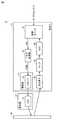
図1は、実施の形態のスマートフォンの主要な構成を表わす図である。
スマートフォン100は、アンテナ2と、無線通信部3と、タッチパネル4と、OLED(Organic Light Emitting Diode)パネル5と、照度センサ6と、スピーカ7と、マイク8と、近接センサ9と、加速度センサ16と、ジャイロセンサ17と、制御回路12と、電池15とを備える。近接センサ9は、発光部10と、受光IC(Integrated Circuit)11とを備える。制御回路12は、プロセッサ13と、メモリ14とを備える。FIG. 1 is a diagram showing a main configuration of a smartphone according to an embodiment.
The
アンテナ2は、基地局へ無線信号を送信し、基地局からの無線信号を受信する。
無線通信部3は、アンテナ2から送られる無線信号を増幅処理およびダウンコンバートして、制御回路12へ出力する。無線通信部3は、制御回路12で生成された音信号等を含む送信信号をアップコンバートおよび増幅処理をして、処理後の無線信号をアンテナ2へ出力する。The
The
タッチパネル4は、ユーザの指などの物体の接触または近接を検出し、その検出結果に応じた検出信号を制御回路12へ出力する。 The
マイク8は、スマートフォン100の外部から入力される音を電気的な音信号に変換して制御回路12に出力する。 The
スピーカ7は、制御回路12からの電気的な音信号を音に変換して出力する。
加速度センサ16は、スマートフォン100の加速度を検出する。The
The
ジャイロセンサ17は、スマートフォン100の回転速度を検出する。
OLEDパネル5は、制御回路12の制御によって、文字、記号、図形などの各種情報を表示する。The
The
照度センサ6は、周辺の環境の照度を検出して、その検出結果に応じた検出信号を制御回路12へ出力する。 The
近接センサ9は、物体の近接を検出し、その検出結果に応じた検出信号を制御回路12へ出力する。制御回路12は、物体の近接が検出されたときには、タッチパネル4およびOLEDパネル5をオフ状態に設定する。 The
発光部10は、赤外光を出射する。
受光IC11は、発光部10による赤外光の出射を制御するとともに、発光部10から出射され、物体によって反射された赤外光を検出する。The
The
プロセッサ13は、CPU(Central Processing Unit)、およびDSP(Digital Signal Processing)などによって構成される。 The
メモリ14は、スマートフォン100を制御するための制御プログラム、および複数のアプリケーションプログラムなどを記憶する。制御回路12の各種機能は、プロセッサ13がメモリ14内の各種プログラムを実行することによって実現される。 The
電池15は、スマートフォン100に含まれる電子部品に電力を供給する。
図2は、液晶パネルを有するスマートフォンの近接センサの配置を表わす図である。The
FIG. 2 is a diagram showing the arrangement of proximity sensors of a smartphone having a liquid crystal panel.
図2に示すように、スマートフォン100の長手方向をY軸方向とする。スマートフォン100の短手方向をX軸とする。スマートフォン100の正面の法線方向をZ軸方向とする。以下の説明では、下側とは、Z軸の負方向、上側とは、Z軸の正方向とする。 As shown in FIG. 2, the longitudinal direction of the
従来の近接センサでは、ベゼル97の下側に受光IC11およびLED(Light Emitting Diod)21を配置する。ベゼル97のエリアに受光IC11およびLED21を配置しなければならないため、ベゼル97の面積が大きくなる。その結果、液晶パネル95の領域が小さくなる。 In the conventional proximity sensor, the
図3は、第1の実施形態の近接センサ9の構成を表わす図である。
受光IC11は、制御ロジック31と、パルス生成器32と、ドライバ33を含む駆動部39と、受光素子34と、アンプ35と、ADC(Analog to Digital Converter)36とを含む。発光部10は、LED(Light Emitting Diode)21を含む。FIG. 3 is a diagram showing the configuration of the
The
制御ロジック31は、プロセッサ13からの指令に従って、LED21の駆動を制御する。制御ロジック31は、赤外光の受光の有無をプロセッサ13へ通知する。 The
パルス生成器32は、パルス幅変調信号PWMを出力する。
ドライバ33は、パルス幅変調信号PWMに従って、LED21を駆動する。The
The
受光素子34は、物体RFで反射された赤外光を検出する。受光素子34は、フォトダイオードによって構成される。 The
アンプ35は、受光素子34の出力信号を増幅する。
ADC36は、アンプ35の出力信号をデジタル信号に変換して、制御ロジック31へ出力する。The
The
図4は、OLEDパネル5の構成の一例を表わす図である。
OLEDパネル5は、基板フィルム71と、無機膜72と、OLED層76と、封止体75と、側部封止体73と、封止フィルム74とを備える。FIG. 4 is a diagram showing an example of the configuration of the
The
基板フィルム71は、高分子材料によって形成されている。無機膜72は、基板フィルム71の上に形成されている。無機膜72は、無機材料によって形成されている。OLED層76は、無機膜72の上に形成されている。OLED層76は、陽極層、陰極層、発光層などの層を有し、複数のOLED素子を有する。封止体75は、無機膜72の上に形成されている。封止体75は、高分子材料を主成分とする材料によって形成されている。封止体75は、OLED層76を包囲して、OLED層76を保護する。封止フィルム74は、封止体75の上部を覆うように形成されている。封止フィルム74は、ガラスまたは金属によって形成されている。側部封止体73は、封止体75の側部を覆うように形成されている。側部封止体73は、高分子材料および添加剤によって形成されている。 The
これらの素子で構成されるOLEDパネル5は、LEDから出射される赤外光に対して3〜10%の透過性を有する。 The
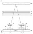
図5は、第1の実施形態の近接センサ9の配置を表わす図である。
第1の実施の形態の近接センサ9では、OLEDパネル5がLEDから出射される赤外光に対して透過性を有するという特性を利用して、OLEDパネル5の下側のOLEDパネル5で覆われる領域に受光IC11とLED21とが配置される。つまり、OLEDパネル5の位置が(x1、y1)〜(x2、y2)で表される矩形領域の場合に、この矩形領域内に受光IC11とLED21とが配置される。FIG. 5 is a diagram showing the arrangement of the
In the
近接センサ9への物体の近接の検出と、タッチパネル4への入力とが同時に発生した場合に、近接センサ9への物体の近接の検出を優先するものとすることができる。 When the detection of the proximity of the object to the
近接センサ9による物体の近接の検出と、タッチパネル4ヘの入力との競合をできるだけ避けるために、OLEDパネル5で覆われる領域のできるだけ隅に受光IC11と、LED21とを配置するものとしてもよい。たとえば、図5に示すように、受光IC11と、LED21とは、右上の隅に配置されるものとしてもよい。また、右上の隅の領域には、ユーザによってタッチ指示される項目を表示しないようにしてもよい。 In order to avoid conflict between the proximity detection of the object by the
受光IC11と、LED21をOLEDパネル5の下側に配置するので、ベゼル97内に受光IC11およびLED21を配置するための領域を確保しなくてもよいため、ベゼル97の面積を小さくすることができる。その結果、OLEDパネル5の面積を大きくすることができる。 Since the
図6は、第1の実施形態の近接センサ9の配置を表わす図である。図5は、XZ平面に平行な面における配置を表わす。 FIG. 6 is a diagram showing the arrangement of the
カバーパネル51の下側にタッチパネル4が配置される。タッチパネル4の下側にOLEDパネル5が配置される。OLEDパネル5の下側に、メイン基板61上が配置される。メイン基板61上に、受光ICモジュール54と、LEDモジュール53とが配置される。 The
受光ICモジュール54は、ベース基板60と、受光IC11と、ケース部材57と、集光部材55とを備える。受光IC11は、メイン基板61と電気的に接続する。集光部材55は、物体RFによって反射された赤外光を集光して、受光IC11内の受光素子34へ送る。 The light receiving
LEDモジュール53は、ベース基板59と、LED21と、ケース部材58と、集光部材56とを備える。LED21は、メイン基板61と電気的に接続する。集光部材56は、LED21から出射された赤外光を集光して、LEDモジュール53の外部へ出力する。 The
LEDモジュール53と、受光ICモジュール54との距離Dは、LED21から出射された赤外光が物体RFで反射されて、戻ってきたときに受光素子34に入力され、かつLED21から出射された赤外光がOLEDパネル5またはタッチパネル4で反射されて、戻ってきたときに受光素子34に入力されないように調整されている。 The distance D between the
以上のように、本実施の形態によれば、表示パネルとしてOLEDパネルを用い、OLEDパネルの下側にLEDと受光ICを配置することによって、ベゼルの面積を小さくすることができる。その結果、OLEDパネルの面積を大きくすることができる。 As described above, according to the present embodiment, the area of the bezel can be reduced by using the OLED panel as the display panel and arranging the LED and the light receiving IC under the OLED panel. As a result, the area of the OLED panel can be increased.
[第2の実施形態]
本実施の形態のスマートフォンでは、近接センサが2つのLEDを備えることによって、1つのLEDのパワーを低減する。[Second Embodiment]
In the smartphone of the present embodiment, the proximity sensor includes two LEDs to reduce the power of one LED.
図7は、第2の実施形態の近接センサ9の構成を表わす図である。
受光IC11は、制御ロジック31と、パルス生成器32と、第1のドライバ33−aおよび第2のドライバ33−bを含む駆動部39と、受光素子34と、アンプ35と、ADC36とを含む。発光部10は、第1のLED21−aと、第2のLED21−bとを含む。FIG. 7 is a diagram showing the configuration of the
The
制御ロジック31は、プロセッサ13からの指令に従って、第1のLED21−aおよび第2のLED21−bの駆動を制御する。制御ロジック31は、赤外光の受光の有無をプロセッサ13へ通知する。 The
パルス生成器32は、第1のパルス幅変調信号PWMaおよび第2のパルス幅変調信号PWMbを出力する。 The
第1のドライバ33−aは、第1のパルス幅変調信号PWMaに従って、第1のLED21−aを駆動する。第2のドライバ33−bは、第2のパルス幅変調信号PWMbに従って、第2のLED21−aを駆動する。 The first driver 33-a drives the first LED 21-a according to the first pulse width modulation signal PWMa. The second driver 33-b drives the second LED 21-a according to the second pulse width modulation signal PWMb.
受光素子34は、物体RFで反射された赤外光を検出する。受光素子34は、フォトダイオードによって構成される。 The
アンプ35は、受光素子34の出力信号を増幅する。
ADC36は、アンプ35の出力信号をデジタル信号に変換して、制御ロジック31へ出力する。The
The
図8は、イネーブル信号EN、第1のパルス幅変調信号PWMa、および第2のパルス幅変調信号PWMbのタイミングチャートである。 FIG. 8 is a timing chart of the enable signal EN, the first pulse width modulation signal PWMa, and the second pulse width modulation signal PWMb.
時刻T1において、制御ロジック31によって、イネーブル信号ENが活性化されると、時刻T1において、パルス生成器32による第1のパルス幅変調信号PWMaおよび第2のパルス幅変調信号PWMbの生成が開始される。これによって、第1のLED21−aからの赤外光の出射の開始タイミングと、第2のLED21−bからの赤外光の出射の開始タイミングとを同時にすることができる。 When the enable signal EN is activated by the
時刻T2において、制御ロジック31によって、イネーブル信号ENが非活性化されると、時刻T2において、パルス生成器32による第1のパルス幅変調信号PWMaおよび第2のパルス幅変調信号PWMbの生成が終了する。これによって、第1のLED21−aからの赤外光の出射の終了タイミングと、第2のLED21−bからの赤外光の出射の終了タイミングとを同時にすることができる。 When the enable signal EN is deactivated by the
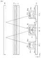
図9は、第2の実施形態の近接センサ9の配置を表わす図である。
第2の実施の形態の近接センサでは、OLEDパネル5の下側のOLEDパネル5で覆われる領域に受光IC11と、第1のLED21−aと第2のLED21−bとが配置される。つまり、OLEDパネル5の位置が(x1、y1)〜(x2、y2)で表される矩形領域の場合に、この矩形領域内に受光IC11と第1のLED21−aと第2のLED21−bとが配置される。第1のLED21−aの中心と、第2のLED21−bの中心とは、受光IC11に含まれる受光素子34の中心と通る直線上に配置される。FIG. 9 is a diagram showing the arrangement of the
In the proximity sensor of the second embodiment, the
第1の実施形態と同様に、第2の実施形態でも、受光IC11と、第1のLED21−aと、第2のLED21−bとをOLEDパネル5の下側に配置するので、ベゼル97内に受光IC11および第1のLED21−a、第2のLED21−bを配置するための領域を確保しなくてもよいため、ベゼル97の面積を小さくすることができる。その結果、OLEDパネル5の面積を大きくすることができる。 Similar to the first embodiment, in the second embodiment, the
2つのLEDから赤外光を出射することによって、1つのLEDのパワーを小さくすることができ、赤外光の出射に伴って発生する熱を分散させることができる。 By emitting infrared light from the two LEDs, the power of one LED can be reduced, and the heat generated by the emission of the infrared light can be dispersed.
図10は、第2の実施形態の近接センサ9の配置を表わす図である。図10は、XZ平面に平行な面における配置を表わす。 FIG. 10 is a diagram showing the arrangement of the
カバーパネル51の下側にタッチパネル4が配置される。タッチパネル4の下側にOLEDパネル5が配置される。OLEDパネル5の下側に、メイン基板61上が配置される。メイン基板61上に、受光ICモジュール54と、第1のLEDモジュール53−aと、第2のLEDモジュール53−bとが配置される。 The
受光ICモジュール54は、ベース基板60と、受光IC11と、ケース部材57と、集光部材55とを備える。受光IC11は、メイン基板61と電気的に接続する。集光部材55は、物体RFによって反射された赤外光を集光して、受光IC11内の受光素子34へ送る。 The light receiving
第1のLEDモジュール53−aは、ベース基板59−aと、第1のLED21−aと、ケース部材58−aと、集光部材56−aとを備える。第1のLED21−aは、メイン基板61と電気的に接続する。集光部材56−aは、第1のLED21−aから出射された赤外光を集光して、第1のLEDモジュール53−aの外部へ出力する。 The first LED module 53-a includes a base substrate 59-a, a first LED 21-a, a case member 58-a, and a light collecting member 56-a. The first LED 21-a is electrically connected to the
第2のLEDモジュール53−bは、ベース基板59−bと、第2のLED21−bと、ケース部材58−bと、集光部材56−bとを備える。第2のLED21−bは、メイン基板61と電気的に接続する。集光部材56−bは、第2のLED21−bから出射された赤外光を集光して、第2のLEDモジュール53−bの外部へ出力する。 The second LED module 53-b includes a base substrate 59-b, a second LED 21-b, a case member 58-b, and a light collecting member 56-b. The second LED 21-b is electrically connected to the
第1のLEDモジュール53−aと受光ICモジュール54との距離Dは、第1のLED21−aから出射された赤外光が物体RFで反射されて、戻ってきたときに受光素子34に入力され、かつ第1のLED21−aから出射された赤外光がOLEDパネル5またはタッチパネル4で反射されて、戻ってきたときに受光素子34に入力されないように調整されている。 The distance D between the first LED module 53-a and the light receiving
第2のLEDモジュール53−bと受光ICモジュール54との距離Dは、第2のLED21−bから出射された赤外光が物体RFで反射されて、戻ってきたときに受光素子34に入力され、かつ第2のLED21−bから出射された赤外光がOLEDパネル5またはタッチパネル4で反射されて、戻ってきたときに受光素子34に入力されないように調整されている。 The distance D between the second LED module 53-b and the light receiving
以上のように、本実施の形態によれば、近接センサを構成するLEDの数を複数個にすることによって、赤外光の出射によって発生する熱を分散させることができる。これによって、OLEDパネルに加わる熱を分散することができる。 As described above, according to the present embodiment, the heat generated by the emission of infrared light can be dispersed by increasing the number of LEDs constituting the proximity sensor to a plurality of LEDs. As a result, the heat applied to the OLED panel can be dispersed.
[第3の実施形態]
図11は、第3の実施形態の近接センサ9の配置を表わす図である。[Third Embodiment]
FIG. 11 is a diagram showing the arrangement of the
第3の実施の形態の近接センサでは、OLEDパネル5の下側に、受光IC11と、第1のLED21−aと、第2のLED21−bと、第3のLED21−cと、第4のLED21−dが配置される。 In the proximity sensor of the third embodiment, the
第1の実施形態と同様に、第3の実施形態でも、受光IC11と、4個のLED21−a,21−b,21−c,21−dをOLEDパネル5の下側のOLEDパネル5で覆われる領域に配置するので、ベゼル97内に受光IC11および4個のLED21−a,21−b,21−c,21−dを配置するための領域を確保しなくてもよいため、ベゼル97の面積を小さくすることができる。その結果、OLEDパネル5の面積を大きくすることができる。 Similar to the first embodiment, in the third embodiment, the
第3の実施形態では、4つのLEDから赤外光を出射することによって、1つのLEDのパワーを小さくすることができ、赤外光の出射に伴って発生する熱を分散させることができる。 In the third embodiment, by emitting infrared light from the four LEDs, the power of one LED can be reduced, and the heat generated by the emission of the infrared light can be dispersed.
第3の実施形態では、複数のLEDのうちの1対のLEDのそれぞれの中心は、受光素子34の中心を中心として点対称の位置に配置される。具体的には、第1のLED21−aの中心と、第3のLED21−cの中心とが、受光素子34の中心を中心として点対称の位置に配置され、第2のLED21−bの中心と、第4のLED21−dの中心とが、受光素子34の中心を中心として点対称の位置に配置される。これによって、赤外光の出射に伴って発生する熱を好適に分散させることができる。 In the third embodiment, the centers of each of the pair of LEDs among the plurality of LEDs are arranged at point-symmetrical positions about the center of the
第1のLED21−a、第2のLED21−b、第3のLED21−c、第4のLED21−dと受光ICモジュール54との距離は、同一のDである。この距離Dは、第1のLED21−a、第2のLED21−b、第3のLED21−c、第4のLED21−dから出射された赤外光が物体RFで反射されて、戻ってきたときに受光素子34に入力され、かつ第1のLED21−a、第2のLED21−b、第3のLED21−c、第4のLED21−dから出射された赤外光がOLEDパネル5またはタッチパネル4で反射されて、戻ってきたときに受光素子34に入力されないように調整されている。 The distances between the first LED21-a, the second LED21-b, the third LED21-c, the fourth LED21-d and the light receiving
以上のように、本実施の形態によれば、近接センサを構成する複数のLEDを点対称に配置することによって、赤外光の出射によって発生する熱を分散させることができる。これによって、OLEDパネルに加わる熱を分散することができる。 As described above, according to the present embodiment, the heat generated by the emission of infrared light can be dispersed by arranging the plurality of LEDs constituting the proximity sensor point-symmetrically. As a result, the heat applied to the OLED panel can be dispersed.
[第4の実施形態]
図12は、第4の実施形態の近接センサ9の配置を表わす図である。[Fourth Embodiment]
FIG. 12 is a diagram showing the arrangement of the
第4の実施の形態の近接センサでは、OLEDパネル5の下側に、受光IC11と、第1のLED21−aと、第2のLED21−bと、第3のLED21−cと、第4のLED21−dと、第5のLED21−eとが配置される。 In the proximity sensor of the fourth embodiment, the
第1の実施形態と同様に、第4の実施形態でも、受光IC11と、5個のLED21−a,21−b,21−c,21−d,21−eをOLEDパネル5の下側のOLEDパネル5で覆われる領域に配置するので、ベゼル97内に受光IC11および5個のLED21−a,21−b,21−c,21−−d,21−eを配置するための領域を確保しなくてもよいため、ベゼル97の面積を小さくすることができる。その結果、OLEDパネル5の面積を大きくすることができる。 Similar to the first embodiment, in the fourth embodiment, the
第4の実施形態では、5つのLEDから赤外光を出射することによって、1つのLEDのパワーを小さくすることができ、赤外光の出射に伴って発生する熱を分散させることができる。 In the fourth embodiment, by emitting infrared light from the five LEDs, the power of one LED can be reduced, and the heat generated by the emission of the infrared light can be dispersed.
第1のLED21−a、第2のLED21−b、第3のLED21−c、第4のLED21−d、第5のLED21−eは、受光素子34の中心を中心とした円上に配置される。隣接するLEDの間の角度θは、同一である。近接センサが5個のLEDを備える場合には、5個のLED21−a,21−b,21−c,21−d,21−cが、θ=72度の間隔で配置される。これによって、赤外光の出射に伴って発生する熱を好適に分散させることができる。 The first LED21-a, the second LED21-b, the third LED21-c, the fourth LED21-d, and the fifth LED21-e are arranged on a circle centered on the center of the
第1のLED21−a、第2のLED21−b、第3のLED21−c、第4のLED21−d、第5のLED21−eと受光ICモジュール54との距離は、同一のDである。この距離Dは、第1のLED21−a、第2のLED21−b、第3のLED21−c、第4のLED21−d、第5のLED21−eから出射された赤外光が物体RFで反射されて、戻ってきたときに受光素子34に入力され、かつ第1のLED21−a、第2のLED21−b、第3のLED21−c、第4のLED21−d、第5のLED21−eから出射された赤外光がOLEDパネル5またはタッチパネル4で反射されて、戻ってきたときに受光素子34に入力されないように調整されている。 The distances between the first LED21-a, the second LED21-b, the third LED21-c, the fourth LED21-d, the fifth LED21-e and the light receiving
以上のように、本実施の形態によれば、近接センサを構成する複数のLEDを円上に等間隔で配置することによって、赤外光の出射によって発生する熱を分散させることができる。これによって、OLEDパネルに加わる熱を分散することができる。 As described above, according to the present embodiment, the heat generated by the emission of infrared light can be dispersed by arranging the plurality of LEDs constituting the proximity sensor at equal intervals on the circle. As a result, the heat applied to the OLED panel can be dispersed.
[第5の実施形態]
図13は、第4の実施形態の近接センサ9の構成を表わす図である。[Fifth Embodiment]
FIG. 13 is a diagram showing the configuration of the
受光IC11は、制御ロジック31と、パルス生成器32と、ドライバ233を含む駆動部39と、受光素子34と、アンプ35と、ADC36とを含む。発光部10は、第1のLED21aと、第2のLED21−bとを含む。 The
制御ロジック31は、プロセッサ13からの指令に従って、第1のLED21−aおよび第2のLED21−bの駆動を制御する。制御ロジック31は、赤外光の受光の有無をプロセッサ13へ通知する。 The
パルス生成器32は、パルス幅変調信号PWMを出力する。
ドライバ233は、パルス幅変調信号PWMに従って、第1のLED21−aおよび第2のLED21−bを駆動する。The
The driver 233 drives the first LED 21-a and the second LED 21-b according to the pulse width modulation signal PWM.
受光素子34は、物体RFで反射された赤外光を検出する。受光素子34は、フォトダイオードによって構成される。 The
アンプ35は、受光素子34の出力信号を増幅する。
ADC36は、アンプ35の出力信号をデジタル信号に変換して、制御ロジック31へ出力する。The
The
以上のように、本実施の形態では、1つのドライバによって、2つのLEDを駆動することができる。 As described above, in the present embodiment, two LEDs can be driven by one driver.
(変形例)
本発明は、上記の実施形態に限定されるものではなく、たとえば、以下のような変形例も含む。(Modification example)
The present invention is not limited to the above embodiment, and includes, for example, the following modifications.
(1)LEDから赤外光が出射され、受光素子が赤外光を検出するものとしたが、これに限定されるものではない。たとえば、LEDから可視光または近赤外光が出射され、受光素子が可視光または近赤外光を検出するものとしてもよい。 (1) Infrared light is emitted from the LED, and the light receiving element detects the infrared light, but the present invention is not limited to this. For example, visible light or near-infrared light may be emitted from the LED, and the light receiving element may detect visible light or near-infrared light.
(2)LEDの数は、上記の実施形態で説明したものに限定されない。近接センサは、3個のLED、または6個以上のLEDを備えるものとしてもよい。 (2) The number of LEDs is not limited to that described in the above embodiment. The proximity sensor may include three LEDs, or six or more LEDs.
今回開示された実施の形態はすべての点で例示であって制限的なものではないと考えられるべきである。本発明の範囲は上記した説明ではなくて特許請求の範囲によって示され、特許請求の範囲と均等の意味および範囲内でのすべての変更が含まれることが意図される。 It should be considered that the embodiments disclosed this time are exemplary in all respects and not restrictive. The scope of the present invention is shown by the scope of claims rather than the above description, and it is intended to include all modifications within the meaning and scope equivalent to the scope of claims.
2 アンテナ、3 無線通信部、4 タッチパネル、5 OLEDパネル、6 照度センサ、7 スピーカ、8 マイク、9 近接センサ、10 発光部、11 受光IC、12 制御回路、13 プロセッサ、14 メモリ、15 電池、16 加速度センサ、17 ジャイロセンサ、21,21−a,21−b,21−c,21−d,21−e LED、31 制御ロジック、32 パルス生成器、33,33−a,33−b,233 ドライバ、34 受光素子、35 アンプ、36 ADC、39 駆動部、51 カバーパネル、53,53−a,53−b LEDモジュール、54 受光ICモジュール、55,56,56−a,56−b 集光部材、57,58,58−a,58−b ケース部材、59,59−a,59−b,60 ベース基板、61 メイン基板、95 液晶パネル、97 ベゼル、100 スマートフォン、RF 物体。 2 antenna, 3 wireless communication unit, 4 touch panel, 5 OLED panel, 6 illuminance sensor, 7 speaker, 8 microphone, 9 proximity sensor, 10 light emitting unit, 11 light receiving IC, 12 control circuit, 13 processor, 14 memory, 15 battery, 16 Acceleration sensor, 17 Gyro sensor, 21,21-a, 21-b, 21-c, 21-d, 21-e LED, 31 Control logic, 32 pulse generator, 33, 33-a, 33-b, 233 driver, 34 light receiving element, 35 amplifier, 36 ADC, 39 drive unit, 51 cover panel, 53, 53-a, 53-b LED module, 54 light receiving IC module, 55, 56, 56-a, 56-b collection Optical member, 57,58,58-a, 58-b case member, 59,59-a, 59-b, 60 base substrate, 61 main substrate, 95 liquid crystal panel, 97 bezel, 100 smartphone, RF object.
Claims (10)
Translated fromJapanese光を出射するLEDを駆動する駆動部と、
反射された光を検出する受光素子とを備え、
前記受光ICは、前記OLEDパネルの下側の前記OLEDパネルで覆われる領域に配置される、受光IC。A light receiving IC that can be mounted on an electronic device having an OLED panel.
A drive unit that drives an LED that emits light,
Equipped with a light receiving element that detects reflected light,
The light receiving IC is arranged in an area covered by the OLED panel below the OLED panel.
各々が、複数の前記LEDのうちの対応する1つのLEDを駆動する複数のドライバを備える、請求項2または3記載の受光IC。The drive unit
The light receiving IC according to claim 2 or 3, each comprising a plurality of drivers for driving one of the plurality of LEDs.
前記LEDとを備えた、近接センサ。The light receiving IC according to claim 1 and
Proximity sensor with the LED.
複数の前記LEDとを備えた、近接センサ。The light receiving IC according to any one of claims 2 to 4,
Proximity sensor with the plurality of LEDs.
請求項5〜9のいずれか1項に記載の近接センサとを備えた、電子機器。With the OLED panel
An electronic device comprising the proximity sensor according to any one of claims 5 to 9.
Priority Applications (3)
| Application Number | Priority Date | Filing Date | Title |
|---|---|---|---|
| JP2019079571AJP2020178052A (en) | 2019-04-18 | 2019-04-18 | Light receiving ICs, proximity sensors, and electronic devices |
| US16/846,679US11227902B2 (en) | 2019-04-18 | 2020-04-13 | Light receiving IC, proximity sensor and electronic machine |
| CN202010293486.8ACN111831165B (en) | 2019-04-18 | 2020-04-15 | Light receiving IC, proximity sensor and electronic equipment |
Applications Claiming Priority (1)
| Application Number | Priority Date | Filing Date | Title |
|---|---|---|---|
| JP2019079571AJP2020178052A (en) | 2019-04-18 | 2019-04-18 | Light receiving ICs, proximity sensors, and electronic devices |
Publications (1)
| Publication Number | Publication Date |
|---|---|
| JP2020178052Atrue JP2020178052A (en) | 2020-10-29 |
Family
ID=72830920
Family Applications (1)
| Application Number | Title | Priority Date | Filing Date |
|---|---|---|---|
| JP2019079571APendingJP2020178052A (en) | 2019-04-18 | 2019-04-18 | Light receiving ICs, proximity sensors, and electronic devices |
Country Status (3)
| Country | Link |
|---|---|
| US (1) | US11227902B2 (en) |
| JP (1) | JP2020178052A (en) |
| CN (1) | CN111831165B (en) |
Families Citing this family (1)
| Publication number | Priority date | Publication date | Assignee | Title |
|---|---|---|---|---|
| CN115768211B (en)* | 2022-10-31 | 2023-12-19 | 芯思杰技术(深圳)股份有限公司 | Display screen and electronic equipment |
Citations (10)
| Publication number | Priority date | Publication date | Assignee | Title |
|---|---|---|---|---|
| US20080297487A1 (en)* | 2007-01-03 | 2008-12-04 | Apple Inc. | Display integrated photodiode matrix |
| US20110248171A1 (en)* | 2010-04-13 | 2011-10-13 | Rueger Timothy T | Apparatus with optical functionality and associated methods |
| US20120162636A1 (en)* | 2010-12-23 | 2012-06-28 | Silicon Laboratories, Inc. | Proximity detector including anti-falsing mechanism |
| JP2016047073A (en)* | 2014-08-27 | 2016-04-07 | 株式会社東芝 | Electronic apparatus and control method |
| JP2017097345A (en)* | 2015-11-18 | 2017-06-01 | 株式会社半導体エネルギー研究所 | Electronic device |
| JP2017111545A (en)* | 2015-12-15 | 2017-06-22 | 株式会社レーザーシステム | Display device |
| US20170364763A1 (en)* | 2016-06-15 | 2017-12-21 | Samsung Electronics Co., Ltd. | Electronic device supporting fingerprint verification function and method for operating the same |
| CN107943345A (en)* | 2017-11-22 | 2018-04-20 | 广东欧珀移动通信有限公司 | Method and device for calibrating proximity sensor, storage medium and electronic equipment |
| US20180364869A1 (en)* | 2017-06-14 | 2018-12-20 | Samsung Electronics Co., Ltd. | Electronic device including light emitting module and light receiving module adjacent to display, and operating method thereof |
| WO2019012046A1 (en)* | 2017-07-14 | 2019-01-17 | Behr-Hella Thermocontrol Gmbh | DISPLAY DEVICE WITH INTEGRATED, OPTICALLY WORKING PROXIMITY SENSOR |
Family Cites Families (1)
| Publication number | Priority date | Publication date | Assignee | Title |
|---|---|---|---|---|
| US9830495B2 (en) | 2015-07-17 | 2017-11-28 | Motorola Mobility Llc | Biometric authentication system with proximity sensor |
- 2019
- 2019-04-18JPJP2019079571Apatent/JP2020178052A/enactivePending
- 2020
- 2020-04-13USUS16/846,679patent/US11227902B2/enactiveActive
- 2020-04-15CNCN202010293486.8Apatent/CN111831165B/enactiveActive
Patent Citations (10)
| Publication number | Priority date | Publication date | Assignee | Title |
|---|---|---|---|---|
| US20080297487A1 (en)* | 2007-01-03 | 2008-12-04 | Apple Inc. | Display integrated photodiode matrix |
| US20110248171A1 (en)* | 2010-04-13 | 2011-10-13 | Rueger Timothy T | Apparatus with optical functionality and associated methods |
| US20120162636A1 (en)* | 2010-12-23 | 2012-06-28 | Silicon Laboratories, Inc. | Proximity detector including anti-falsing mechanism |
| JP2016047073A (en)* | 2014-08-27 | 2016-04-07 | 株式会社東芝 | Electronic apparatus and control method |
| JP2017097345A (en)* | 2015-11-18 | 2017-06-01 | 株式会社半導体エネルギー研究所 | Electronic device |
| JP2017111545A (en)* | 2015-12-15 | 2017-06-22 | 株式会社レーザーシステム | Display device |
| US20170364763A1 (en)* | 2016-06-15 | 2017-12-21 | Samsung Electronics Co., Ltd. | Electronic device supporting fingerprint verification function and method for operating the same |
| US20180364869A1 (en)* | 2017-06-14 | 2018-12-20 | Samsung Electronics Co., Ltd. | Electronic device including light emitting module and light receiving module adjacent to display, and operating method thereof |
| WO2019012046A1 (en)* | 2017-07-14 | 2019-01-17 | Behr-Hella Thermocontrol Gmbh | DISPLAY DEVICE WITH INTEGRATED, OPTICALLY WORKING PROXIMITY SENSOR |
| CN107943345A (en)* | 2017-11-22 | 2018-04-20 | 广东欧珀移动通信有限公司 | Method and device for calibrating proximity sensor, storage medium and electronic equipment |
Also Published As
| Publication number | Publication date |
|---|---|
| US20200335555A1 (en) | 2020-10-22 |
| CN111831165A (en) | 2020-10-27 |
| CN111831165B (en) | 2024-11-12 |
| US11227902B2 (en) | 2022-01-18 |
Similar Documents
| Publication | Publication Date | Title |
|---|---|---|
| EP2909864B1 (en) | Electronic devices with display-integrated light sensors | |
| CN111433708B (en) | Electronic device with light absorbing member between display panel and ultrasonic sensor | |
| KR20200064573A (en) | Electronic device inlcuding a flexible display, and method of operating the same | |
| US20080211183A1 (en) | Computer Controlled Pawn | |
| EP3735612B1 (en) | Display including plurality of wiring layers in bending region | |
| CN107316568A (en) | A kind of flexible display apparatus | |
| US11216115B2 (en) | Electronic device and method for controlling touch sensing signals and storage medium | |
| US20230343266A1 (en) | Grayscale controlling method and display panel | |
| US12228967B2 (en) | Electronic device including photosensor module | |
| KR20250004588A (en) | DISPLAY PANEL, MANUFACTURING METHOD THEREOF AND ElECTRONIC DEVICE INCLUDING SAME | |
| WO2011129159A1 (en) | Input display device, input device, and control method of input device | |
| KR20210008238A (en) | Electronic apparatus | |
| JP2020178052A (en) | Light receiving ICs, proximity sensors, and electronic devices | |
| EP4141935A1 (en) | Electronic device comprising sensor | |
| KR102706216B1 (en) | Electronic device for controlling optical sensor module and operating method thereof | |
| JP2013246476A (en) | Touch panel | |
| CN110848597B (en) | Lighting assembly, terminal equipment and working state control method | |
| CN113710017A (en) | Electronic device | |
| JP7209584B2 (en) | Light-receiving sensors, proximity sensors, and electronics | |
| CN201926995U (en) | Remote input device | |
| WO2022183673A1 (en) | Display panel, terminal device, and display | |
| CN112859441A (en) | Display device | |
| JP2021150671A (en) | Light receiving ICs, proximity sensors, and electronic devices | |
| CN113571007B (en) | Sub-pixel driving circuit and pixel driving circuit | |
| KR20210097255A (en) | Electronic device and method of medsuring biometric information using same |
Legal Events
| Date | Code | Title | Description |
|---|---|---|---|
| A621 | Written request for application examination | Free format text:JAPANESE INTERMEDIATE CODE: A621 Effective date:20220323 | |
| A977 | Report on retrieval | Free format text:JAPANESE INTERMEDIATE CODE: A971007 Effective date:20221228 | |
| A131 | Notification of reasons for refusal | Free format text:JAPANESE INTERMEDIATE CODE: A131 Effective date:20230110 | |
| A521 | Request for written amendment filed | Free format text:JAPANESE INTERMEDIATE CODE: A523 Effective date:20230214 | |
| A131 | Notification of reasons for refusal | Free format text:JAPANESE INTERMEDIATE CODE: A131 Effective date:20230516 | |
| A521 | Request for written amendment filed | Free format text:JAPANESE INTERMEDIATE CODE: A523 Effective date:20230628 | |
| A02 | Decision of refusal | Free format text:JAPANESE INTERMEDIATE CODE: A02 Effective date:20230912 |