JP2020170852A - Semiconductor device - Google Patents
Semiconductor deviceDownload PDFInfo
- Publication number
- JP2020170852A JP2020170852AJP2020104406AJP2020104406AJP2020170852AJP 2020170852 AJP2020170852 AJP 2020170852AJP 2020104406 AJP2020104406 AJP 2020104406AJP 2020104406 AJP2020104406 AJP 2020104406AJP 2020170852 AJP2020170852 AJP 2020170852A
- Authority
- JP
- Japan
- Prior art keywords
- oxide semiconductor
- thin film
- layer
- film transistor
- semiconductor region
- Prior art date
- Legal status (The legal status is an assumption and is not a legal conclusion. Google has not performed a legal analysis and makes no representation as to the accuracy of the status listed.)
- Withdrawn
Links
Images


Classifications
- H—ELECTRICITY
- H10—SEMICONDUCTOR DEVICES; ELECTRIC SOLID-STATE DEVICES NOT OTHERWISE PROVIDED FOR
- H10D—INORGANIC ELECTRIC SEMICONDUCTOR DEVICES
- H10D30/00—Field-effect transistors [FET]
- H10D30/60—Insulated-gate field-effect transistors [IGFET]
- H10D30/67—Thin-film transistors [TFT]
- H10D30/674—Thin-film transistors [TFT] characterised by the active materials
- H10D30/6755—Oxide semiconductors, e.g. zinc oxide, copper aluminium oxide or cadmium stannate
- H—ELECTRICITY
- H01—ELECTRIC ELEMENTS
- H01L—SEMICONDUCTOR DEVICES NOT COVERED BY CLASS H10
- H01L21/00—Processes or apparatus adapted for the manufacture or treatment of semiconductor or solid state devices or of parts thereof
- H01L21/02—Manufacture or treatment of semiconductor devices or of parts thereof
- H01L21/02104—Forming layers
- H01L21/02365—Forming inorganic semiconducting materials on a substrate
- H01L21/02518—Deposited layers
- H01L21/02521—Materials
- H01L21/02551—Group 12/16 materials
- H01L21/02554—Oxides
- H—ELECTRICITY
- H01—ELECTRIC ELEMENTS
- H01L—SEMICONDUCTOR DEVICES NOT COVERED BY CLASS H10
- H01L21/00—Processes or apparatus adapted for the manufacture or treatment of semiconductor or solid state devices or of parts thereof
- H01L21/02—Manufacture or treatment of semiconductor devices or of parts thereof
- H01L21/02104—Forming layers
- H01L21/02365—Forming inorganic semiconducting materials on a substrate
- H01L21/02518—Deposited layers
- H01L21/02521—Materials
- H01L21/02565—Oxide semiconducting materials not being Group 12/16 materials, e.g. ternary compounds
- H—ELECTRICITY
- H01—ELECTRIC ELEMENTS
- H01L—SEMICONDUCTOR DEVICES NOT COVERED BY CLASS H10
- H01L21/00—Processes or apparatus adapted for the manufacture or treatment of semiconductor or solid state devices or of parts thereof
- H01L21/02—Manufacture or treatment of semiconductor devices or of parts thereof
- H01L21/02104—Forming layers
- H01L21/02365—Forming inorganic semiconducting materials on a substrate
- H01L21/02612—Formation types
- H01L21/02617—Deposition types
- H01L21/02631—Physical deposition at reduced pressure, e.g. MBE, sputtering, evaporation
- H—ELECTRICITY
- H10—SEMICONDUCTOR DEVICES; ELECTRIC SOLID-STATE DEVICES NOT OTHERWISE PROVIDED FOR
- H10D—INORGANIC ELECTRIC SEMICONDUCTOR DEVICES
- H10D30/00—Field-effect transistors [FET]
- H10D30/01—Manufacture or treatment
- H10D30/021—Manufacture or treatment of FETs having insulated gates [IGFET]
- H10D30/031—Manufacture or treatment of FETs having insulated gates [IGFET] of thin-film transistors [TFT]
- H—ELECTRICITY
- H10—SEMICONDUCTOR DEVICES; ELECTRIC SOLID-STATE DEVICES NOT OTHERWISE PROVIDED FOR
- H10D—INORGANIC ELECTRIC SEMICONDUCTOR DEVICES
- H10D30/00—Field-effect transistors [FET]
- H10D30/60—Insulated-gate field-effect transistors [IGFET]
- H10D30/67—Thin-film transistors [TFT]
- H—ELECTRICITY
- H10—SEMICONDUCTOR DEVICES; ELECTRIC SOLID-STATE DEVICES NOT OTHERWISE PROVIDED FOR
- H10D—INORGANIC ELECTRIC SEMICONDUCTOR DEVICES
- H10D30/00—Field-effect transistors [FET]
- H10D30/60—Insulated-gate field-effect transistors [IGFET]
- H10D30/67—Thin-film transistors [TFT]
- H10D30/6704—Thin-film transistors [TFT] having supplementary regions or layers in the thin films or in the insulated bulk substrates for controlling properties of the device
- H—ELECTRICITY
- H10—SEMICONDUCTOR DEVICES; ELECTRIC SOLID-STATE DEVICES NOT OTHERWISE PROVIDED FOR
- H10D—INORGANIC ELECTRIC SEMICONDUCTOR DEVICES
- H10D30/00—Field-effect transistors [FET]
- H10D30/60—Insulated-gate field-effect transistors [IGFET]
- H10D30/67—Thin-film transistors [TFT]
- H10D30/6757—Thin-film transistors [TFT] characterised by the structure of the channel, e.g. transverse or longitudinal shape or doping profile
- H—ELECTRICITY
- H10—SEMICONDUCTOR DEVICES; ELECTRIC SOLID-STATE DEVICES NOT OTHERWISE PROVIDED FOR
- H10D—INORGANIC ELECTRIC SEMICONDUCTOR DEVICES
- H10D62/00—Semiconductor bodies, or regions thereof, of devices having potential barriers
- H10D62/10—Shapes, relative sizes or dispositions of the regions of the semiconductor bodies; Shapes of the semiconductor bodies
- H10D62/124—Shapes, relative sizes or dispositions of the regions of semiconductor bodies or of junctions between the regions
- H—ELECTRICITY
- H10—SEMICONDUCTOR DEVICES; ELECTRIC SOLID-STATE DEVICES NOT OTHERWISE PROVIDED FOR
- H10D—INORGANIC ELECTRIC SEMICONDUCTOR DEVICES
- H10D62/00—Semiconductor bodies, or regions thereof, of devices having potential barriers
- H10D62/80—Semiconductor bodies, or regions thereof, of devices having potential barriers characterised by the materials
- H—ELECTRICITY
- H10—SEMICONDUCTOR DEVICES; ELECTRIC SOLID-STATE DEVICES NOT OTHERWISE PROVIDED FOR
- H10D—INORGANIC ELECTRIC SEMICONDUCTOR DEVICES
- H10D64/00—Electrodes of devices having potential barriers
- H10D64/60—Electrodes characterised by their materials
- H10D64/62—Electrodes ohmically coupled to a semiconductor
- H—ELECTRICITY
- H10—SEMICONDUCTOR DEVICES; ELECTRIC SOLID-STATE DEVICES NOT OTHERWISE PROVIDED FOR
- H10D—INORGANIC ELECTRIC SEMICONDUCTOR DEVICES
- H10D84/00—Integrated devices formed in or on semiconductor substrates that comprise only semiconducting layers, e.g. on Si wafers or on GaAs-on-Si wafers
- H10D84/01—Manufacture or treatment
- H—ELECTRICITY
- H10—SEMICONDUCTOR DEVICES; ELECTRIC SOLID-STATE DEVICES NOT OTHERWISE PROVIDED FOR
- H10D—INORGANIC ELECTRIC SEMICONDUCTOR DEVICES
- H10D86/00—Integrated devices formed in or on insulating or conducting substrates, e.g. formed in silicon-on-insulator [SOI] substrates or on stainless steel or glass substrates
- H10D86/40—Integrated devices formed in or on insulating or conducting substrates, e.g. formed in silicon-on-insulator [SOI] substrates or on stainless steel or glass substrates characterised by multiple TFTs
- H10D86/60—Integrated devices formed in or on insulating or conducting substrates, e.g. formed in silicon-on-insulator [SOI] substrates or on stainless steel or glass substrates characterised by multiple TFTs wherein the TFTs are in active matrices
- H—ELECTRICITY
- H10—SEMICONDUCTOR DEVICES; ELECTRIC SOLID-STATE DEVICES NOT OTHERWISE PROVIDED FOR
- H10D—INORGANIC ELECTRIC SEMICONDUCTOR DEVICES
- H10D99/00—Subject matter not provided for in other groups of this subclass
- H—ELECTRICITY
- H10—SEMICONDUCTOR DEVICES; ELECTRIC SOLID-STATE DEVICES NOT OTHERWISE PROVIDED FOR
- H10D—INORGANIC ELECTRIC SEMICONDUCTOR DEVICES
- H10D86/00—Integrated devices formed in or on insulating or conducting substrates, e.g. formed in silicon-on-insulator [SOI] substrates or on stainless steel or glass substrates
- H10D86/40—Integrated devices formed in or on insulating or conducting substrates, e.g. formed in silicon-on-insulator [SOI] substrates or on stainless steel or glass substrates characterised by multiple TFTs
- H10D86/421—Integrated devices formed in or on insulating or conducting substrates, e.g. formed in silicon-on-insulator [SOI] substrates or on stainless steel or glass substrates characterised by multiple TFTs having a particular composition, shape or crystalline structure of the active layer
- H10D86/423—Integrated devices formed in or on insulating or conducting substrates, e.g. formed in silicon-on-insulator [SOI] substrates or on stainless steel or glass substrates characterised by multiple TFTs having a particular composition, shape or crystalline structure of the active layer comprising semiconductor materials not belonging to the Group IV, e.g. InGaZnO
Landscapes
- Engineering & Computer Science (AREA)
- Condensed Matter Physics & Semiconductors (AREA)
- General Physics & Mathematics (AREA)
- Manufacturing & Machinery (AREA)
- Computer Hardware Design (AREA)
- Microelectronics & Electronic Packaging (AREA)
- Power Engineering (AREA)
- Physics & Mathematics (AREA)
- Thin Film Transistor (AREA)
- Liquid Crystal (AREA)
- Electroluminescent Light Sources (AREA)
- Electrodes Of Semiconductors (AREA)
- Physical Vapour Deposition (AREA)
- Physical Deposition Of Substances That Are Components Of Semiconductor Devices (AREA)
- Devices For Indicating Variable Information By Combining Individual Elements (AREA)
- Electrochromic Elements, Electrophoresis, Or Variable Reflection Or Absorption Elements (AREA)
Abstract
Translated fromJapaneseDescription
Translated fromJapanese本発明は、酸化物半導体を用いる半導体装置と、該半導体装置を用いた表示装置及びそれ
らの作製方法に関する。The present invention relates to a semiconductor device using an oxide semiconductor, a display device using the semiconductor device, and a method for manufacturing the same.
近年、液晶ディスプレイに代表される液晶表示装置が広く普及していきている。液晶ディ
スプレイとしては、各画素に薄膜トランジスタ(TFT)が設けられたアクティブマトリ
クス型のものがよく用いられている。アクティブマトリクス型液晶ディスプレイの薄膜ト
ランジスタには、活性層としてアモルファスシリコンや多結晶シリコン用いられる。アモ
ルファスシリコンを用いた薄膜トランジスタは、電界効果移動度が低いが、大型ガラス基
板のような大面積基板にも容易に形成することができる。一方、多結晶シリコンを用いた
薄膜トランジスタは電界効果移動度が高いが、レーザアニール等の結晶化工程が必要なの
で、大型ガラス基板のような大面積基板に形成するには膨大な時間がかかる。In recent years, liquid crystal display devices typified by liquid crystal displays have become widespread. As the liquid crystal display, an active matrix type in which a thin film transistor (TFT) is provided in each pixel is often used. Amorphous silicon and polycrystalline silicon are used as the active layer in the thin film transistor of the active matrix liquid crystal display. A thin film transistor using amorphous silicon has low field effect mobility, but can be easily formed on a large area substrate such as a large glass substrate. On the other hand, a thin film transistor using polycrystalline silicon has a high field effect mobility, but requires a crystallization step such as laser annealing, so that it takes an enormous amount of time to form a large area substrate such as a large glass substrate.
これに対し、上記のようなシリコン材料に代わって、酸化物半導体を用いて薄膜トランジ
スタを作製し、電子デバイスや光デバイスに応用する技術が注目されている。例えば、酸
化物半導体層として酸化亜鉛、In−Ga−Zn−O系酸化物半導体を用いて薄膜トラン
ジスタを作製し、画像表示装置のスイッチング素子などに用いる技術が特許文献1及び特
許文献2で開示されている。On the other hand, a technique of producing a thin film transistor using an oxide semiconductor instead of the above-mentioned silicon material and applying it to an electronic device or an optical device is attracting attention. For example,
上述の酸化物半導体層の電気的特性は、酸化物半導体層の組成や膜質や界面などに大きく
影響を受ける。そして酸化物半導体層の組成や膜質や界面などは、大気中への暴露や不純
物を含む膜との接触により、容易に変化し得る。The electrical characteristics of the oxide semiconductor layer described above are greatly affected by the composition, film quality, interface, and the like of the oxide semiconductor layer. The composition, film quality, interface, etc. of the oxide semiconductor layer can be easily changed by exposure to the atmosphere or contact with a film containing impurities.
大気中の酸素や水分が薄膜トランジスタの酸化物半導体層に侵入するのを防ぐために、酸
化物半導体層上にシリコンを主成分とする酸化物(酸化シリコン)や窒化物(窒化シリコ
ン)などからなる保護絶縁層が形成されている。Protection of oxide (silicon oxide) and nitride (silicon nitride) containing silicon as the main component on the oxide semiconductor layer to prevent oxygen and moisture in the atmosphere from entering the oxide semiconductor layer of the thin film transistor. An insulating layer is formed.
しかし、シリコンを主成分とする保護絶縁層の形成だけでは、酸化物半導体層の組成や膜
質や界面などを安定化させるには不十分である。However, the formation of the protective insulating layer containing silicon as a main component is not sufficient to stabilize the composition, film quality, interface, etc. of the oxide semiconductor layer.
また、酸化物半導体層をパターニングする際に形成されるレジストマスクやレジスト剥離
溶液が酸化物半導体層に接触することによっても、酸化物半導体層の膜質や組成が変化す
る恐れがある。In addition, the film quality and composition of the oxide semiconductor layer may change when the resist mask or resist stripping solution formed when patterning the oxide semiconductor layer comes into contact with the oxide semiconductor layer.
以上のように、酸化物半導体層の組成や膜質や界面などの変化に伴い、酸化物半導体層を
用いた薄膜トランジスタの電気的特性も変化するという問題がある。As described above, there is a problem that the electrical characteristics of the thin film transistor using the oxide semiconductor layer also change with changes in the composition, film quality, interface, and the like of the oxide semiconductor layer.
本発明の一態様は、薄膜トランジスタを形成するにあたって、活性層として第1の酸化物
半導体領域を用い、第1の酸化物半導体領域と薄膜トランジスタの保護絶縁層との間に、
第1の酸化物半導体領域より導電率が低く、第1の酸化物半導体領域の保護層として機能
する第2の酸化物半導体領域を形成することを要旨とする。In one aspect of the present invention, a first oxide semiconductor region is used as an active layer in forming a thin film transistor, and between the first oxide semiconductor region and the protective insulating layer of the thin film transistor,
The gist is to form a second oxide semiconductor region which has a lower conductivity than the first oxide semiconductor region and functions as a protective layer of the first oxide semiconductor region.
本発明の一態様は、ゲート電極層と、ゲート電極層上にゲート絶縁層と、ゲート絶縁層上
にソース電極層及びドレイン電極層と、ソース電極層及びドレイン電極層上に第1の酸化
物半導体領域と、第1の酸化物半導体領域上に第2の酸化物半導体領域とを有し、第1の
酸化物半導体領域の一部は、ソース電極層とドレイン電極層の間で、ゲート絶縁層と、ソ
ース電極層及びドレイン電極層の側面部と接し、第2の酸化物半導体領域の導電率は、第
1の酸化物半導体領域の導電率より小さく、第1の酸化物半導体領域とソース電極層及び
ドレイン電極層とは電気的に接続することを特徴とする半導体装置である。One aspect of the present invention is a gate electrode layer, a gate insulating layer on the gate electrode layer, a source electrode layer and a drain electrode layer on the gate insulating layer, and a first oxide on the source electrode layer and the drain electrode layer. It has a semiconductor region and a second oxide semiconductor region on the first oxide semiconductor region, and a part of the first oxide semiconductor region is gate-insulated between the source electrode layer and the drain electrode layer. The layer is in contact with the side surface portions of the source electrode layer and the drain electrode layer, and the conductivity of the second oxide semiconductor region is smaller than that of the first oxide semiconductor region, and the first oxide semiconductor region and the source The electrode layer and the drain electrode layer are semiconductor devices characterized by being electrically connected.
本発明の他の一態様は、ゲート電極層と、ゲート電極層上にゲート絶縁層と、ゲート絶縁
層上にソース電極層及びドレイン電極層と、ソース電極層及びドレイン電極層上にn型の
導電型を有するバッファ層と、n型の導電型を有するバッファ層上に第1の酸化物半導体
領域と、第1の酸化物半導体領域上に第2の酸化物半導体領域とを有し、第1の酸化物半
導体領域の一部は、ソース電極層とドレイン電極層の間で、ゲート絶縁層と、ソース電極
層及びドレイン電極層の側面部と接し、バッファ層のキャリア濃度は、第1の酸化物半導
体領域のキャリア濃度より高く、第2の酸化物半導体領域の導電率は、第1の酸化物半導
体領域の導電率より小さく、バッファ層の導電率は、第1の酸化物半導体領域及び第2の
酸化物半導体領域の導電率より高く、第1の酸化物半導体領域とソース電極層及びドレイ
ン電極層の上面とはバッファ層を介して電気的に接続することを特徴とする半導体装置で
ある。Another aspect of the present invention is a gate electrode layer, a gate insulating layer on the gate electrode layer, a source electrode layer and a drain electrode layer on the gate insulating layer, and an n-type on the source electrode layer and the drain electrode layer. It has a first oxide semiconductor region on a buffer layer having a conductive type, a buffer layer having an n-type conductive type, and a second oxide semiconductor region on a first oxide semiconductor region. A part of the oxide semiconductor region of 1 is in contact with the gate insulating layer and the side surface portions of the source electrode layer and the drain electrode layer between the source electrode layer and the drain electrode layer, and the carrier concentration of the buffer layer is the first. Higher than the carrier concentration in the oxide semiconductor region, the conductivity of the second oxide semiconductor region is smaller than that of the first oxide semiconductor region, and the conductivity of the buffer layer is higher than that of the first oxide semiconductor region and A semiconductor device characterized in that the conductivity is higher than that of the second oxide semiconductor region, and the first oxide semiconductor region and the upper surfaces of the source electrode layer and the drain electrode layer are electrically connected via a buffer layer. is there.
本発明の他の一態様は、ゲート電極層と、ゲート電極層上にゲート絶縁層と、ゲート絶縁
層上にソース電極層及びドレイン電極層と、ソース電極層及びドレイン電極層上に酸化物
半導体層とを有し、酸化物半導体層の一部は、ソース電極層とドレイン電極層の間で、ゲ
ート絶縁層と、ソース電極層及びドレイン電極層の側面部と接し、酸化物半導体層はイン
ジウム、ガリウム、亜鉛またはスズのうち少なくとも一つを含む酸化物半導体層であり、
酸化物半導体層の一部は、絶縁層を介してソース電極層及びドレイン電極層の側面部と接
し、酸化物半導体層とソース電極層及びドレイン電極層とは電気的に接続することを特徴
とする半導体装置である。Another aspect of the present invention is a gate electrode layer, a gate insulating layer on the gate electrode layer, a source electrode layer and a drain electrode layer on the gate insulating layer, and an oxide semiconductor on the source electrode layer and the drain electrode layer. It has a layer, and a part of the oxide semiconductor layer is in contact with the gate insulating layer and the side surface portions of the source electrode layer and the drain electrode layer between the source electrode layer and the drain electrode layer, and the oxide semiconductor layer is indium. , An oxide semiconductor layer containing at least one of gallium, zinc or tin,
A part of the oxide semiconductor layer is in contact with the side surface portions of the source electrode layer and the drain electrode layer via an insulating layer, and the oxide semiconductor layer and the source electrode layer and the drain electrode layer are electrically connected to each other. It is a semiconductor device.
なお、第1の酸化物半導体領域、第2の酸化物半導体領域及びバッファ層はインジウム、
ガリウム、亜鉛またはスズのうち少なくとも一つを含むことが好ましい。また、第2の酸
化物半導体領域の酸素空孔欠陥密度は、第1の酸化物半導体領域の酸素空孔欠陥密度より
小さいことが好ましい。また、第1の酸化物半導体領域と第2の酸化物半導体領域が異な
る酸化物半導体層として形成されてもよいし、同一の酸化物半導体層に形成されてもよい
。The first oxide semiconductor region, the second oxide semiconductor region, and the buffer layer are indium.
It preferably contains at least one of gallium, zinc or tin. Further, the oxygen vacancies defect density of the second oxide semiconductor region is preferably smaller than the oxygen vacancies defect density of the first oxide semiconductor region. Further, the first oxide semiconductor region and the second oxide semiconductor region may be formed as different oxide semiconductor layers, or may be formed in the same oxide semiconductor layer.
なお、第2の酸化物半導体領域の導電率は、1.0×10⁻⁸S/cm以下であることが
好ましい。また、バッファ層のキャリア濃度は、1×10¹⁸/cm3以上であることが
好ましい。The conductivity of the second oxide semiconductor region is preferably 1.0 ×10⁻⁸ S / cm or less. The carrier concentration of the buffer layer is preferably 1 × 10¹⁸ / cm3 or more.
また、第1の酸化物半導体領域の一部は、酸化膜を介してソース電極層及びドレイン電極
層の側面部と接することが好ましい。また、酸化膜は、熱酸化、酸素プラズマ処理または
オゾン水処理によって形成されることが好ましい。Further, it is preferable that a part of the first oxide semiconductor region is in contact with the side surface portions of the source electrode layer and the drain electrode layer via the oxide film. Further, the oxide film is preferably formed by thermal oxidation, oxygen plasma treatment or ozone water treatment.
また、第1の酸化物半導体領域の一部は、サイドウォール絶縁層を介してソース電極層及
びドレイン電極層の側面部と接することが好ましい。また、サイドウォール絶縁層は、シ
リコン膜、酸化シリコン膜、窒化酸化シリコン膜または酸化窒化シリコン膜で形成される
ことが好ましい。Further, it is preferable that a part of the first oxide semiconductor region is in contact with the side surface portions of the source electrode layer and the drain electrode layer via the sidewall insulating layer. Further, the sidewall insulating layer is preferably formed of a silicon film, a silicon oxide film, a silicon nitride film or a silicon nitride film.
本発明の他の一態様は、基板上にゲート電極層を形成し、ゲート電極層上にゲート絶縁層
を形成し、ゲート絶縁層上に導電膜を成膜し、導電膜をエッチングしてソース電極層及び
ドレイン電極層を形成し、ゲート絶縁層、ソース電極層及びドレイン電極層上に第1の酸
化物半導体膜をスパッタ法によって成膜し、第1の酸化物半導体膜上に第2の酸化物半導
体膜をスパッタ法によって成膜し、第1の酸化物半導体膜及び第2の酸化物半導体膜をエ
ッチングして第1の酸化物半導体領域及び第2の酸化物半導体領域を形成し、第1の酸化
物半導体領域の一部が、ソース電極層とドレイン電極層の間で、ゲート絶縁層と、ソース
電極層及びドレイン電極層の側面部と接するように第1の酸化物半導体領域を設け、第2
の酸化物半導体膜の成膜時の酸素ガス流量の比率を、第1の酸化物半導体膜の成膜時の酸
素ガス流量の比率より多くすることを特徴とする半導体装置の作製方法である。In another aspect of the present invention, a gate electrode layer is formed on a substrate, a gate insulating layer is formed on the gate electrode layer, a conductive film is formed on the gate insulating layer, and the conductive film is etched to be a source. An electrode layer and a drain electrode layer are formed, a first oxide semiconductor film is formed on the gate insulating layer, the source electrode layer and the drain electrode layer by a sputtering method, and a second oxide semiconductor film is formed on the first oxide semiconductor film. The oxide semiconductor film is formed by a sputtering method, and the first oxide semiconductor film and the second oxide semiconductor film are etched to form the first oxide semiconductor region and the second oxide semiconductor region. The first oxide semiconductor region is formed so that a part of the first oxide semiconductor region is in contact with the gate insulating layer and the side surface portions of the source electrode layer and the drain electrode layer between the source electrode layer and the drain electrode layer. Provided, second
This is a method for manufacturing a semiconductor device, characterized in that the ratio of the oxygen gas flow rate at the time of forming the oxide semiconductor film is larger than the ratio of the oxygen gas flow rate at the time of forming the first oxide semiconductor film.
なお、第1の酸化物半導体膜及び第2の酸化物半導体膜が、インジウム、ガリウム、亜鉛
またはスズのうち少なくとも一つを含むことが好ましい。また、第1の酸化物半導体膜と
第2の酸化物半導体膜を、酸素ガスの流量を増やしながら一括して成膜してもよい。また
、第1の酸化物半導体膜の成膜時の酸素ガス流量の比率を70体積%未満とし、第2の酸
化物半導体膜の成膜時の酸素ガス流量の比率を70体積%以上とすることが好ましい。The first oxide semiconductor film and the second oxide semiconductor film preferably contain at least one of indium, gallium, zinc, and tin. Further, the first oxide semiconductor film and the second oxide semiconductor film may be formed together while increasing the flow rate of oxygen gas. Further, the ratio of the oxygen gas flow rate at the time of forming the first oxide semiconductor film is set to less than 70% by volume, and the ratio of the oxygen gas flow rate at the time of forming the second oxide semiconductor film is set to 70% by volume or more. Is preferable.
なお、第1、第2として付される序数詞は便宜上用いるものであり、工程順又は積層順を
示すものではない。また、本明細書において発明を特定するための事項として固有の名称
を示すものではない。The ordinal numbers attached as the first and second numbers are used for convenience and do not indicate the process order or the stacking order. In addition, this specification does not indicate a unique name as a matter for specifying the invention.
なお、本明細書中において半導体装置とは、半導体特性を利用することで機能しうる装置
全般を指し、電気光学装置、半導体回路および電子機器は全て半導体装置である。In the present specification, the semiconductor device refers to all devices that can function by utilizing the semiconductor characteristics, and the electro-optical device, the semiconductor circuit, and the electronic device are all semiconductor devices.
本発明の一態様は、第1の酸化物半導体領域を活性層として用いた薄膜トランジスタにお
いて、第1の酸化物半導体領域と薄膜トランジスタの保護絶縁層との間に、第1の酸化物
半導体より導電率が低く、保護層として機能する第2の酸化物半導体領域を形成すること
によって、第2の酸化物半導体領域は、第1の酸化物半導体領域の組成の変化や膜質の劣
化を防ぎ、薄膜トランジスタの電気的特性を安定させることができる。One aspect of the present invention is that in a thin film using the first oxide semiconductor region as an active layer, the conductivity between the first oxide semiconductor region and the protective insulating layer of the thin film is higher than that of the first oxide semiconductor. By forming a second oxide semiconductor region that has a low value and functions as a protective layer, the second oxide semiconductor region prevents changes in the composition of the first oxide semiconductor region and deterioration of the film quality, and forms a thin film. The electrical characteristics can be stabilized.
該薄膜トランジスタを表示装置の画素部及び駆動回路部に用いることによって、電気特性
が高く信頼性のよい表示装置を提供することができる。By using the thin film transistor for the pixel portion and the drive circuit portion of the display device, it is possible to provide a display device having high electrical characteristics and high reliability.
実施の形態について、図面を用いて詳細に説明する。但し、本発明は以下の説明に限定さ
れず、本発明の趣旨及びその範囲から逸脱することなくその形態及び詳細を様々に変更し
得ることは当業者であれば容易に理解される。従って、本発明は以下に示す実施の形態の
記載内容に限定して解釈されるものではない。なお、以下に説明する発明の構成において
、同一部分又は同様な機能を有する部分には同一の符号を異なる図面間で共通して用い、
その繰り返しの説明は省略する。The embodiment will be described in detail with reference to the drawings. However, the present invention is not limited to the following description, and it is easily understood by those skilled in the art that the form and details of the present invention can be variously changed without departing from the spirit and scope of the present invention. Therefore, the present invention is not construed as being limited to the description of the embodiments shown below. In the configuration of the invention described below, the same reference numerals are commonly used between different drawings for the same parts or parts having similar functions.
The repeated description will be omitted.
(実施の形態1)
本実施の形態では、薄膜トランジスタの構造について、図1を用いて説明する。(Embodiment 1)
In the present embodiment, the structure of the thin film transistor will be described with reference to FIG.
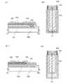
本実施の形態のボトムゲート構造の薄膜トランジスタを図1に示す。図1(A)は断面図
であり、図1(B)は平面図である。図1(A)は、図1(B)における線A1−A2の
断面図となっている。The thin film transistor having the bottom gate structure of the present embodiment is shown in FIG. FIG. 1 (A) is a cross-sectional view, and FIG. 1 (B) is a plan view. FIG. 1 (A) is a cross-sectional view of lines A1-A2 in FIG. 1 (B).
図1に示す薄膜トランジスタには、基板100上にゲート電極層101が設けられ、ゲー
ト電極層101上にゲート絶縁層102が設けられ、ゲート絶縁層102上にソース電極
層又はドレイン電極層105a、105bが設けられ、ゲート絶縁層102と、ソース電
極層又はドレイン電極層105a、105b上に第1の酸化物半導体領域103が設けら
れ、第1の酸化物半導体領域103上に、第1の酸化物半導体領域103より導電率の低
い第2の酸化物半導体領域104が設けられている。なお、第1の酸化物半導体領域10
3と第2の酸化物半導体領域104は、同一の酸化物半導体層中に一緒に形成されてもよ
いし、異なる酸化物半導体層として別々に形成されてもよい。また、第1の酸化物半導体
領域103と第2の酸化物半導体領域104の間に、導電率が段階的又は連続的に変化す
る酸化物半導体の中間領域が存在してもよい。また、酸化物半導体中間領域は、第1の酸
化物半導体領域103及び第2の酸化物半導体領域104と、同一の酸化物半導体層中に
一緒に形成されてもよいし、異なる酸化物半導体層として別々に形成されてもよい。In the thin film transistor shown in FIG. 1, a
The third and second
ゲート電極層101は、アルミニウム、銅、モリブデン、チタン、クロム、タンタル、タ
ングステン、ネオジム、スカンジウムなどの金属材料、またはこれらの金属材料を主成分
とする合金材料、またはこれらの金属材料を成分とする窒化物を用いて、単層又は積層で
形成する。アルミニウムや銅などの低抵抗導電性材料で形成するのが望ましいが、耐熱性
が低い、または腐食しやすいという問題点があるので耐熱性導電性材料と組み合わせて用
いるのが好ましい。耐熱性導電性材料としては、モリブデン、チタン、クロム、タンタル
、タングステン、ネオジム、スカンジウム等を用いる。The
例えば、ゲート電極層101の積層構造としては、アルミニウム層上にモリブデン層が積
層された二層の積層構造、または銅層上にモリブデン層を積層した二層構造、または銅層
上に窒化チタン層若しくは窒化タンタル層を積層した二層構造、窒化チタン層とモリブデ
ン層とを積層した二層構造とすることが好ましい。3層の積層構造としては、タングステ
ン層または窒化タングステン層と、アルミニウムとシリコンの合金層またはアルミニウム
とチタンの合金層と、窒化チタン層またはチタン層とを積層した構造とすることが好まし
い。For example, the laminated structure of the
第1の酸化物半導体領域103及び第2の酸化物半導体領域104を形成する酸化物半導
体層としては、InMO3(ZnO)m(m>0)で表記される構造の酸化物半導体を用
いるのが好ましく、特にIn−Ga−Zn−O系酸化物半導体を用いるのが好ましい。な
お、Mは、ガリウム(Ga)、鉄(Fe)、ニッケル(Ni)、マンガン(Mn)及びコ
バルト(Co)から選ばれた一の金属元素又は複数の金属元素を示す。例えばMとして、
Gaの場合があることの他、GaとNi又はGaとFeなど、Ga以外の上記金属元素が
含まれる場合がある。また、上記酸化物半導体において、Mとして含まれる金属元素の他
に、不純物元素としてFe、Niその他の遷移金属元素、又は該遷移金属の酸化物が含ま
れているものがある。本明細書においては、InMO3(ZnO)m(m>0)で表記さ
れる構造の酸化物半導体のうち、Mとして少なくともGaを含む構造の酸化物半導体をI
n−Ga−Zn−O系酸化物半導体と呼び、該薄膜をIn−Ga−Zn−O系非単結晶膜
とも呼ぶ。As the oxide semiconductor layer forming the first
In addition to the case of Ga, the above metal elements other than Ga such as Ga and Ni or Ga and Fe may be contained. In addition to the metal element contained as M, some of the oxide semiconductors contain Fe, Ni or other transition metal elements, or oxides of the transition metal as impurity elements. In the present specification, among the oxide semiconductors having a structure represented by InMO3 (ZnO)m (m> 0), the oxide semiconductor having a structure containing at least Ga as M is referred to as I.
It is called an n-Ga-Zn-O-based oxide semiconductor, and the thin film is also called an In-Ga-Zn-O-based non-single crystal film.
In−Ga−Zn−O系非単結晶膜の結晶構造は、アモルファス構造がXRD(X線回折
)の分析では観察される。なお、In−Ga−Zn−O系非単結晶膜は、スパッタ法で成
膜した後、200℃〜500℃、代表的には300〜400℃で10分〜100分熱処理
を行っている。As for the crystal structure of the In-Ga-Zn-O system non-single crystal film, the amorphous structure is observed by XRD (X-ray diffraction) analysis. The In-Ga-Zn-O non-single crystal film is formed by a sputtering method and then heat-treated at 200 ° C. to 500 ° C., typically 300 to 400 ° C. for 10 minutes to 100 minutes.
In−Ga−Zn−O系非単結晶膜を薄膜トランジスタの活性層として用いることにより
、ゲート電圧±20Vにおいて、オンオフ比が109以上、移動度が10以上の電気的特
性を有する薄膜トランジスタを作製することができる。By using the In-Ga-Zn-O based non-single-crystal film as an active layer of a thin film transistor, the gate voltage ± 20V, the on-off ratio is 109 or more, and a thin film transistor mobility has 10 or more electrical characteristics be able to.
ただし、第1の酸化物半導体領域103及び第2の酸化物半導体領域104を形成する酸
化物半導体層は、InMO3(ZnO)m(m>0)で表記される構造の酸化物半導体層
に限られるものではなく、インジウム、ガリウム、亜鉛またはスズのうち少なくとも一つ
を含めばよい。例えば、酸化亜鉛(ZnO)、酸化錫(SnO)、酸化インジウム亜鉛(
IZO)、酸化インジウムスズ(ITO)、酸化珪素を含む酸化インジウムスズ(ITS
O)、ガリウムを添加した酸化亜鉛(GZO)等からなる酸化物半導体層を用いてもよい
。However, the oxide semiconductor layer forming the first
IZO), indium tin oxide (ITO), indium tin oxide containing silicon oxide (ITS)
An oxide semiconductor layer made of zinc oxide (GZO) or the like to which O) or gallium is added may be used.
また、第1の酸化物半導体領域103の一部が、ソース電極層又はドレイン電極層105
a、105bの間で、ゲート絶縁層102と、ソース電極層又はドレイン電極層105a
、105bの側面部と接するように、第1の酸化物半導体領域103は設けられている。
第1の酸化物半導体領域103の厚さは、10nm〜300nmとし、好ましくは20n
m〜100nmとする。Further, a part of the first
Between a and 105b, the
, 105b, the first
The thickness of the first
It is set to m to 100 nm.
第1の酸化物半導体領域103の導電率は1.0×10⁻⁸S/cm以上であることが好
ましい。また、第1の酸化物半導体領域103の導電率は1.0×10⁻³S/cm未満
であることが好ましい。第1の酸化物半導体領域103のキャリア濃度範囲は1×101
7/cm3未満(より好ましくは1×1011/cm3以上)が好ましい。第1の酸化物
半導体領域103のキャリア濃度範囲が上記の範囲を超えると、薄膜トランジスタがノー
マリーオンとなる恐れがある。The conductivity of the first
It is preferably less than7 / cm3 (more preferably 1 × 10¹¹ / cm3 or more). If the carrier concentration range of the first
また、第1の酸化物半導体領域103中のナトリウム濃度は5×10¹⁹/cm3以下と
し、好ましくは、1×10¹⁸/cm3以下とする。The sodium concentration in the first
第2の酸化物半導体領域104は、第1の酸化物半導体領域103より導電率が小さいも
のとし、第2の酸化物半導体領域104の導電率は1.0×10⁻⁸S/cmより小さい
ことが好ましい。また、第2の酸化物半導体領域104は、第1の酸化物半導体領域10
3より酸素空孔欠陥密度が小さいことが好ましい。酸化物半導体中の酸素空孔欠陥が酸化
物半導体の導電率に寄与するからである。また、第2の酸化物半導体領域104の厚さは
5nm以上1000nm以下が好ましく、10nm以上100nm以下だとさらに好まし
い。The second
It is preferable that the oxygen vacancies defect density is smaller than 3. This is because oxygen vacancies in the oxide semiconductor contribute to the conductivity of the oxide semiconductor. The thickness of the second
第1の酸化物半導体領域103のスパッタ成膜における成膜ガス全体に対する酸素ガス流
量の比率よりも、第2の酸化物半導体領域104のスパッタ成膜における成膜ガス全体に
対する酸素ガス流量の比率を大きくすることによって、第1の酸化物半導体領域103よ
り第2の酸化物半導体領域104の酸素空孔欠陥密度を減少させ、導電率を小さくするこ
とができる。第2の酸化物半導体領域104の成膜条件は、成膜ガス全体に対する酸素ガ
ス流量の比率を70体積%以上とするのが好ましい。また、第1の酸化物半導体領域10
3の成膜条件は、成膜ガス全体に対する酸素ガスの比率を70体積%未満とするのが好ま
しい。The ratio of the oxygen gas flow rate to the entire film formation gas in the sputter film formation of the second
As for the film forming condition of 3, the ratio of oxygen gas to the entire film forming gas is preferably less than 70% by volume.
第1の酸化物半導体領域103と第2の酸化物半導体領域104は、連続的に形成するこ
とができるので、表示装置作製の効率化を図り、生産性を向上することができる。また、
第1の酸化物半導体領域103と第2の酸化物半導体領域104を連続的に成膜すること
によって、第1の酸化物半導体領域103の上面を大気にさらすことなく、第1の酸化物
半導体領域103のパターニングを行うことができる。Since the first
By continuously forming the first
また、第1の酸化物半導体領域103と第2の酸化物半導体領域104を酸素ガスの流量
を増やしながら一括して成膜することによって、第1の酸化物半導体領域103と第2の
酸化物半導体領域104の導電率を連続的に変化させることもできる。Further, by forming the first
第1の酸化物半導体領域103は、薄膜トランジスタの活性層として機能する。一方、第
1の酸化物半導体領域103より導電率の低い第2の酸化物半導体領域104は、第1の
酸化物半導体領域103の大気中への曝露や、酸化物半導体の組成や膜質を変質させる不
純物を含む膜との接触を防ぐ保護層として機能する。よって、チャネル形成領域を有し、
薄膜トランジスタの電気的特性を決定する第1の酸化物半導体領域103は、組成や膜質
の類似する第2の酸化物半導体領域104と接するので、不純物による組成や膜質や界面
などの変化を防ぐことができる。また、保護層として機能する第2の酸化物半導体領域1
04は、酸化物半導体の組成や膜質を変質させる不純物を含む膜と接するが、第1の酸化
物半導体領域103より導電率が低いので、薄膜トランジスタの電気的特性には影響を及
ぼさない。The first
Since the first
Although 04 is in contact with a film containing impurities that alter the composition and film quality of the oxide semiconductor, it does not affect the electrical characteristics of the thin film transistor because its conductivity is lower than that of the first
以上より、第1の酸化物半導体領域を活性層として用いた薄膜トランジスタにおいて、第
1の酸化物半導体領域と薄膜トランジスタの保護絶縁層との間に、第1の酸化物半導体領
域より導電率が低く、保護層として機能する第2の酸化物半導体領域を形成することで、
第1の酸化物半導体領域の組成の変化や膜質の劣化を防ぎ、薄膜トランジスタの電気的特
性を安定させることができる。From the above, in the thin film transistor using the first oxide semiconductor region as the active layer, the conductivity between the first oxide semiconductor region and the protective insulating layer of the thin film transistor is lower than that of the first oxide semiconductor region. By forming a second oxide semiconductor region that functions as a protective layer,
It is possible to prevent changes in the composition of the first oxide semiconductor region and deterioration of the film quality, and to stabilize the electrical characteristics of the thin film transistor.
ソース電極層又はドレイン電極層105a、105bは、第1の導電膜112a、112
b、第2の導電膜113a、113b、第3の導電膜114a、114bからなる3層構
造となっている。第1の導電膜112a、112b〜第3の導電膜114a、114bの
材料としては、アルミニウム、銅、モリブデン、チタン、クロム、タンタル、タングステ
ン、ネオジム、スカンジウムなどの金属材料、またはこれらの金属材料を主成分とする合
金材料、またはこれらの金属材料を成分とする窒化物を用いることができる。アルミニウ
ムや銅などの低抵抗導電性材料で形成するのが望ましいが、耐熱性が低い、または腐食し
やすいという問題点があるので耐熱性導電性材料と組み合わせて用いるのが好ましい。耐
熱性導電性材料としては、モリブデン、チタン、クロム、タンタル、タングステン、ネオ
ジム、スカンジウム等を用いる。The source electrode layer or
It has a three-layer structure including b, the second
例えば、第1の導電膜112a、112b及び第3の導電膜114a、114bに耐熱性
導電性材料であるチタンを用い、第2の導電膜113a、113bに低抵抗である、ネオ
ジムを含むアルミニウム合金を用いるのが好ましい。このような構成にすることで、アル
ミニウムの低抵抗性を活かしつつ、ヒロックの発生を低減することができる。なお、本実
施の形態では、ソース電極層又はドレイン電極層105a、105bを第1の導電膜11
2a、112b、第2の導電膜113a、113b、第3の導電膜114a、114bか
らなる3層構造としたが、これに限られることはなく、単層構造としてもよいし、2層構
造としてもよいし、4層以上の構造としてもよい。For example, an aluminum alloy containing neodymium, which uses titanium as a heat-resistant conductive material for the first
A three-layer structure including 2a, 112b, a second
以上のような構成とすることによって、第1の酸化物半導体領域を活性層として用いた薄
膜トランジスタにおいて、第1の酸化物半導体領域と薄膜トランジスタの保護絶縁層との
間に、第1の酸化物半導体領域より導電率が低く、保護層として機能する第2の酸化物半
導体領域を形成することで、第1の酸化物半導体領域の組成の変化や膜質の劣化を防ぎ、
薄膜トランジスタの電気的特性を安定させることができる。With the above configuration, in a thin film using the first oxide semiconductor region as an active layer, a first oxide semiconductor is formed between the first oxide semiconductor region and the protective insulating layer of the thin film. By forming a second oxide semiconductor region that has lower conductivity than the region and functions as a protective layer, changes in the composition of the first oxide semiconductor region and deterioration of the film quality can be prevented.
The electrical characteristics of the thin film transistor can be stabilized.
なお、本実施の形態に示す構成は、他の実施の形態に示した構成を適宜組み合わせて用い
ることができることとする。It should be noted that the configuration shown in this embodiment can be used in combination with the configurations shown in other embodiments as appropriate.
(実施の形態2)
本実施の形態では、実施の形態1で示した薄膜トランジスタを含む表示装置の作製工程に
ついて、図2乃至図9を用いて説明する。図2と図3は断面図で、図4乃至図7は平面図
となっており、図4乃至図7の線A1−A2及び線B1−B2は、図2及び図3の断面図
に示す線A1−A2、線B1−B2に対応している。(Embodiment 2)
In the present embodiment, the manufacturing process of the display device including the thin film transistor shown in the first embodiment will be described with reference to FIGS. 2 to 9. 2 and 3 are sectional views, FIGS. 4 to 7 are plan views, and lines A1-A2 and B1-B2 of FIGS. 4 to 7 are shown in sectional views of FIGS. 2 and 3. It corresponds to the lines A1-A2 and B1-B2.
まず、基板100を準備する。基板100は、バリウムホウケイ酸ガラス、アルミノホウ
ケイ酸ガラス、若しくはアルミノシリケートガラスなど、フュージョン法やフロート法で
作製される無アルカリガラス基板、セラミック基板の他、本作製工程の処理温度に耐えう
る耐熱性を有するプラスチック基板等を用いることができる。また、ステンレス合金など
の金属基板の表面に絶縁膜を設けた基板を適用しても良い。基板100の大きさは、32
0mm×400mm、370mm×470mm、550mm×650mm、600mm×
720mm、680mm×880mm、730mm×920mm、1000mm×120
0mm、1100mm×1250mm、1150mm×1300mm、1500mm×1
800mm、1900mm×2200mm、2160mm×2460mm、2400mm
×2800mm、又は2850mm×3050mm等を用いることができる。First, the
0 mm x 400 mm, 370 mm x 470 mm, 550 mm x 650 mm, 600 mm x
720 mm, 680 mm x 880 mm, 730 mm x 920 mm, 1000 mm x 120
0 mm, 1100 mm x 1250 mm, 1150 mm x 1300 mm, 1500 mm x 1
800mm, 1900mm x 2200mm, 2160mm x 2460mm, 2400mm
× 2800 mm, 2850 mm × 3050 mm and the like can be used.
また基板100上に下地膜として絶縁膜を形成してもよい。下地膜としては、CVD法や
スパッタ法等を用いて、酸化シリコン膜、窒化シリコン膜、酸化窒化シリコン膜、または
窒化酸化シリコン膜の単層、又は積層で形成すればよい。基板100としてガラス基板の
ような可動イオンを含有する基板を用いる場合、下地膜として窒化シリコン膜、窒化酸化
シリコン膜などの窒素を含有する膜を用いることで、可動イオンが酸化物半導体層に侵入
することを防ぐことができる。Further, an insulating film may be formed on the
次に、ゲート電極層101を含むゲート配線、容量配線108、及び第1の端子121を
形成するための導電膜をスパッタ法や真空蒸着法で基板100全面に成膜する。次いで、
第1のフォトリソグラフィ工程を行い、レジストマスクを形成し、エッチングにより不要
な部分を除去して配線及び電極(ゲート電極層101を含むゲート配線、容量配線108
、及び第1の端子121)を形成する。このとき段切れ防止のために、少なくともゲート
電極層101の端部にテーパー形状が形成されるようにエッチングするのが好ましい。こ
の段階での断面図を図2(A)に示した。なお、この段階での平面図が図4に相当する。Next, a conductive film for forming the gate wiring including the
The first photolithography step is performed, a resist mask is formed, unnecessary parts are removed by etching, and wiring and electrodes (gate wiring including the
, And the first terminal 121). At this time, in order to prevent step breakage, it is preferable to perform etching so that a tapered shape is formed at least at the end of the
ゲート電極層101を含むゲート配線と容量配線108、端子部の第1の端子121は、
実施の形態1で示した導電性材料を用いて単層又は積層で形成することができる。The gate wiring including the
It can be formed in a single layer or in a laminated manner using the conductive material shown in the first embodiment.
次いで、ゲート電極層101上にゲート絶縁層102を全面に成膜する。ゲート絶縁層1
02はCVD法やスパッタ法などを用い、膜厚を50〜250nmとする。Next, the
In 02, a CVD method, a sputtering method, or the like is used, and the film thickness is set to 50 to 250 nm.
例えば、ゲート絶縁層102としてCVD法やスパッタ法により酸化シリコン膜を用い、
100nmの厚さで形成する。勿論、ゲート絶縁層102はこのような酸化シリコン膜に
限定されるものでなく、酸化窒化シリコン膜、窒化酸化シリコン膜、窒化シリコン膜、酸
化アルミニウム膜、酸化タンタル膜などの他の絶縁膜を用い、これらの材料から成る単層
または積層構造として形成しても良い。For example, a silicon oxide film is used as the
It is formed with a thickness of 100 nm. Of course, the
また、ゲート絶縁層102として、有機シランガスを用いたCVD法により酸化シリコン
層を形成することも可能である。有機シランガスとしては、珪酸エチル(TEOS:化学
式Si(OC2H5)4)、テトラメチルシラン(TMS:化学式Si(CH3)4)、
テトラメチルシクロテトラシロキサン(TMCTS)、オクタメチルシクロテトラシロキ
サン(OMCTS)、ヘキサメチルジシラザン(HMDS)、トリエトキシシラン(Si
H(OC2H5)3)、トリスジメチルアミノシラン(SiH(N(CH3)2)3)等
のシリコン含有化合物を用いることができる。Further, as the
Tetramethylcyclotetrasiloxane (TMCTS), octamethylcyclotetrasiloxane (OMCTS), hexamethyldisilazane (HMDS), triethoxysilane (Si)
Silicon-containing compounds such as H (OC2 H5 )3 ) and trisdimethylaminosilane (SiH (N (CH3 )2 )3 ) can be used.
また、ゲート絶縁層102として、アルミニウム、イットリウム、又はハフニウムの酸化
物、窒化物、酸化窒化物、又は窒化酸化物の一種又はそれらの化合物を少なくとも2種以
上含む化合物を用いることもできる。Further, as the
なお、本明細書において、酸化窒化物とは、その組成として、窒素原子よりも酸素原子の
数が多い物質のことを指し、窒化酸化物とは、その組成として、酸素原子より窒素原子の
数が多い物質のことを指す。例えば、酸化窒化シリコン膜とは、その組成として、窒素原
子よりも酸素原子の数が多く、ラザフォード後方散乱法(RBS:Rutherford
Backscattering Spectrometry)及び水素前方散乱法(H
FS:Hydrogen Forward Scattering)を用いて測定した場
合に、濃度範囲として酸素が50〜70原子%、窒素が0.5〜15原子%、シリコンが
25〜35原子%、水素が0.1〜10原子%の範囲で含まれるものをいう。また、窒化
酸化シリコン膜とは、その組成として、酸素原子より窒素原子の数が多く、RBS及びH
FSを用いて測定した場合に、濃度範囲として酸素が5〜30原子%、窒素が20〜55
原子%、シリコンが25〜35原子%、水素が10〜30原子%の範囲で含まれるものを
いう。但し、酸化窒化シリコンまたは窒化酸化シリコンを構成する原子の合計を100原
子%としたとき、窒素、酸素、シリコン及び水素の含有比率が上記の範囲内に含まれるも
のとする。In the present specification, the oxide nitride refers to a substance having a larger number of oxygen atoms than the nitrogen atom in its composition, and the nitride oxide has a composition of more nitrogen atoms than the oxygen atom. Refers to substances with a lot of oxygen. For example, a silicon oxide film has a larger number of oxygen atoms than nitrogen atoms in its composition, and is Rutherford backscattering method (RBS).
Backscattering Spectrometery) and hydrogen forward scattering method (H)
When measured using FS: Hydrogen Forward Scattering), the concentration range is 50 to 70 atomic% for oxygen, 0.5 to 15 atomic% for nitrogen, 25 to 35 atomic% for silicon, and 0.1 to 10 for hydrogen. Those included in the atomic% range. Further, the silicon nitride film has a larger number of nitrogen atoms than oxygen atoms as its composition, and has RBS and H.
When measured using FS, the concentration range is 5 to 30 atomic% for oxygen and 20 to 55 for nitrogen.
Atomic%, silicon is contained in the range of 25 to 35 atomic%, and hydrogen is contained in the range of 10 to 30 atomic%. However, when the total of the atoms constituting silicon oxide or silicon nitride oxide is 100 atomic%, the content ratios of nitrogen, oxygen, silicon and hydrogen shall be included in the above range.
次いで、第2のフォトリソグラフィ工程を行い、ゲート絶縁層102上にレジストマスク
を形成し、エッチングにより不要な部分を除去してゲート電極層101と同じ材料の配線
や電極層に達するコンタクトホールをゲート絶縁層102に形成する。このコンタクトホ
ールは後に形成する導電膜と直接接続するために設ける。例えば、端子部の第1の端子1
21と電気的に接続する端子を形成する場合にコンタクトホールを形成する。Next, a second photolithography step is performed, a resist mask is formed on the
A contact hole is formed when forming a terminal electrically connected to 21.
次に、ゲート絶縁層102上に金属材料からなる第1の導電膜112、第2の導電膜11
3、第3の導電膜114をスパッタ法や真空蒸着法で成膜する。この段階での断面図を図
2(B)に示す。Next, a first
The third
第1の導電膜112、第2の導電膜113、第3の導電膜114の材料としては、実施の
形態1で示した導電性材料を用いて単層又は積層で形成することができる。本実施の形態
では、第1の導電膜112及び第3の導電膜114として耐熱性導電性材料であるチタン
を用い、第2の導電膜113としてネオジムを含むアルミニウム合金を用いる。このよう
な構成にすることで、アルミニウムの低抵抗性を活かしつつ、ヒロックの発生を低減する
ことができる。As the material of the first
次に、第3のフォトリソグラフィ工程を行い、レジストマスク131を形成し、エッチン
グにより不要な部分を除去してソース電極層又はドレイン電極層105a、105b、及
び接続電極120を形成する。この際のエッチング方法としてウェットエッチングまたは
ドライエッチングを用いる。例えば、第1の導電膜112及び第3の導電膜114にチタ
ンを、第2の導電膜113にネオジムを含むアルミニウム合金を用いる場合には、過酸化
水素水、加熱塩酸、またはフッ化アンモニウムを含む硝酸水溶液をエッチャントに用いて
ウェットエッチングすることができる。例えば、KSMF―240(関東化学社製)を用
いて、第1の導電膜112〜第3の導電膜114を一括でエッチングすることができる。Next, a third photolithography step is performed to form a resist
また、第1の導電膜112〜第3の導電膜114のエッチングを過酸化水素水、加熱塩酸
またはフッ化アンモニウムを含む硝酸水溶液をエッチャントとするエッチングで一度に行
うことができるため、ソース電極層又はドレイン電極層105a、105bの各導電膜の
端部は一致し、連続的な構造とすることができる。また、ソース電極層又はドレイン電極
層105a、105bの端部をテーパー状にエッチングすることで、第1の酸化物半導体
領域103の被覆性を向上し、段差形状による第1の酸化物半導体領域103の段切れを
防ぐことができる。この段階での断面図を図2(C)に示す。なお、この段階での平面図
が図5に相当する。Further, since the etching of the first
また、この第3のフォトリソグラフィ工程において、ソース電極層又はドレイン電極層1
05a、105bと同じ材料である第2の端子122を端子部に残す。なお、第2の端子
122はソース配線(ソース電極層又はドレイン電極層105a、105bを含むソース
配線)と電気的に接続されている。Further, in this third photolithography step, the source electrode layer or the
The
また、端子部において、接続電極120は、ゲート絶縁層102に形成されたコンタクト
ホールを介して端子部の第1の端子121と直接接続される。Further, in the terminal portion, the
次に、ゲート絶縁層102、ソース電極層又はドレイン電極層105a、105bに表面
処理を行う。表面処理としては、不活性ガス又は反応性ガスを用いたプラズマ処理等を行
うことができる。Next, the
レジストマスク131を除去した後、基板100が設置されたチャンバー内でアルゴンガ
スを導入してプラズマを発生させて逆スパッタを行い、ゲート絶縁層102の表面に付着
している不純物を除去する。また、逆スパッタを行うことにより、ゲート絶縁層102表
面の平坦性を向上させることもできる。この段階での断面図を図2(D)に示す。逆スパ
ッタとは、ターゲット側に電圧を印加せずに、アルゴン雰囲気下で基板側にRF電源を用
いて電圧を印加して基板にプラズマを形成して表面を改質する方法である。なお、アルゴ
ン雰囲気に代えて窒素、ヘリウムなどを用いてもよい。また、アルゴン雰囲気に酸素、水
素、N2Oなどを加えた雰囲気で行ってもよい。また、アルゴン雰囲気にCl2、CF4
などを加えた雰囲気で行ってもよい。逆スパッタ処理後、大気に曝すことなく第1の酸化
物半導体膜を成膜することによって、ゲート絶縁層102と第1の酸化物半導体領域10
3の界面にゴミや水分が付着するのを防ぐことができる。After removing the resist
You may go in an atmosphere that adds such things. After the reverse sputtering treatment, the
It is possible to prevent dust and moisture from adhering to the interface of 3.
次に、第1の酸化物半導体領域103及び第2の酸化物半導体領域104を形成する酸化
物半導体膜を成膜する。本実施の形態では、第1の酸化物半導体領域103と第2の酸化
物半導体領域104とを異なる酸化物半導体層で形成する。まず、ゲート絶縁層102上
に、第1の酸化物半導体領域103を形成するための第1の酸化物半導体膜を、スパッタ
法を用いてアルゴンなどの希ガスと酸素ガスの雰囲気下で成膜する。第1の酸化物半導体
膜としては、実施の形態1で示した酸化物半導体を用いることができ、In−Ga−Zn
−O系酸化物半導体を用いるのが好ましい。第1の酸化物半導体膜の具体的な成膜条件例
としては、直径8インチのIn、Ga、及びZnを含む酸化物半導体ターゲット(In2
O3:Ga2O3:ZnO=1:1:1)を用いて、基板とターゲットの間との距離を1
70mm、圧力0.4Pa、直流(DC)電源0.5kW、成膜ガスAr:O2=50:
5(sccm)、成膜温度を室温としてスパッタ成膜を行う。また、ターゲットとしては
、In2O3を含む直径8インチの円盤上にペレット状のGa2O3とZnOを配置する
ようにしてもよい。なお、パルス直流(DC)電源を用いると、ゴミを軽減でき、膜厚分
布も均一となるために好ましい。第1の酸化物半導体膜の膜厚は、10nm〜300nm
とし、好ましくは20nm〜100nmとする。Next, an oxide semiconductor film forming the first
It is preferable to use an −O oxide semiconductor. As a specific example of the film forming conditions of the first oxide semiconductor film, an oxide semiconductor target containing In, Ga, and Zn having a diameter of 8 inches (In2).
Using O3 : Ga2 O3 : ZnO = 1: 1: 1), the distance between the substrate and the target is 1
70 mm, pressure 0.4 Pa, direct current (DC) power supply 0.5 kW, film formation gas Ar: O2 = 50:
5 (sccm), sputter film formation is performed with the film formation temperature set to room temperature. Further, as the target, pelletized Ga2 O3 and Zn O may be arranged on a disk having a diameter of 8 inches including In2 O3 . It is preferable to use a pulsed direct current (DC) power source because dust can be reduced and the film thickness distribution becomes uniform. The film thickness of the first oxide semiconductor film is 10 nm to 300 nm.
It is preferably 20 nm to 100 nm.
次いで、大気に曝すことなく、第2の酸化物半導体領域104を形成するための第2の酸
化物半導体膜を、スパッタ法を用いてアルゴンなどの希ガスと酸素ガスの雰囲気下で成膜
する。第2の酸化物半導体膜としては、実施の形態1で示した酸化物半導体を用いること
ができ、In−Ga−Zn−O系酸化物半導体を用いるのが好ましい。第1の酸化物半導
体膜の成膜後、大気に曝すことなく第2の酸化物半導体膜を成膜することによって、第1
の酸化物半導体領域103と第2の酸化物半導体領域104の界面にゴミや水分が吸着し
、第1の酸化物半導体領域103の膜質や組成が変化するのを防ぐことができる。第2の
酸化物半導体膜の具体的な成膜条件例としては、直径8インチのIn、Ga、及びZnを
含む酸化物半導体ターゲット(In2O3:Ga2O3:ZnO=1:1:1)を用いて
、基板とターゲットの間との距離を170mm、圧力0.4Pa、直流(DC)電源0.
5kW、成膜ガスAr:O2=50:1(sccm)、成膜温度を室温としてスパッタ成
膜を行う。また、ターゲットとしては、In2O3を含む直径8インチの円盤上にペレッ
ト状のGa2O3とZnOを配置するようにしてもよい。なお、パルス直流(DC)電源
を用いると、ごみが軽減でき、膜厚分布も均一となるために好ましい。第2の酸化物半導
体膜の膜厚は、5nm〜1000nmとし、好ましくは10nm〜100nmとする。Next, a second oxide semiconductor film for forming the second
It is possible to prevent dust and moisture from adsorbing at the interface between the
Sputter film formation is performed with 5 kW, film formation gas Ar: O2 = 50: 1 (sccm), and the film formation temperature at room temperature. Further, as the target, pelletized Ga2 O3 and Zn O may be arranged on a disk having a diameter of 8 inches including In2 O3 . It is preferable to use a pulsed direct current (DC) power source because dust can be reduced and the film thickness distribution becomes uniform. The film thickness of the second oxide semiconductor film is 5 nm to 1000 nm, preferably 10 nm to 100 nm.
ここで、第1の酸化物半導体膜のスパッタ成膜における成膜ガス全体に対する酸素ガス流
量の比率よりも、第2の酸化物半導体膜のスパッタ成膜における成膜ガス全体に対する酸
素ガス流量の比率を大きくする。これによって、第1の酸化物半導体膜より第2の酸化物
半導体膜の導電率を小さくすることができる。また、第2の酸化物半導体膜の成膜条件は
、成膜ガス全体に対する酸素ガス流量の比率を70体積%以上とするのが好ましい。第1
の酸化物半導体膜の成膜条件は、成膜ガス全体に対する酸素ガスの比率を70体積%未満
とするのが好ましい。Here, the ratio of the oxygen gas flow rate to the entire film-forming gas in the sputter film formation of the second oxide semiconductor film is rather than the ratio of the oxygen gas flow rate to the entire film-forming gas in the sputter film formation of the first oxide semiconductor film. To increase. As a result, the conductivity of the second oxide semiconductor film can be made smaller than that of the first oxide semiconductor film. Further, as the film forming condition of the second oxide semiconductor film, it is preferable that the ratio of the oxygen gas flow rate to the entire film forming gas is 70% by volume or more. 1st
As for the film forming conditions of the oxide semiconductor film, the ratio of oxygen gas to the entire film forming gas is preferably less than 70% by volume.
なお、本実施の形態では、第1の酸化物半導体領域103及び第2の酸化物半導体領域1
04を形成する酸化物半導体膜を異なる酸化物半導体膜として形成したが、本発明はこれ
に限定されるものではない。第1の酸化物半導体領域103を形成する第1の酸化物半導
体膜と第2の酸化物半導体領域104を形成する第2の酸化物半導体膜を、酸素ガスの流
量を連続的に増やしながら一括して成膜することによって、導電率が連続的に変化する同
一の酸化物半導体膜として形成することもできる。また、酸素ガスの流量を段階的に増や
しながら酸化物半導体膜を複数回成膜することによって、第1の酸化物半導体領域103
を形成する第1の酸化物半導体膜と第2の酸化物半導体領域104を形成する第2の酸化
物半導体膜の間に、導電率が段階的に変化する複数の酸化物半導体膜を形成することもで
きる。In the present embodiment, the first
The oxide semiconductor film forming 04 is formed as a different oxide semiconductor film, but the present invention is not limited thereto. The first oxide semiconductor film forming the first
A plurality of oxide semiconductor films whose conductivity changes stepwise are formed between the first oxide semiconductor film forming the above and the second oxide semiconductor film forming the second
また、第1の酸化物半導体膜と第2の酸化物半導体膜とを連続して成膜することができる
ので、表示装置作製の効率化を図り、生産性を向上することができる。Further, since the first oxide semiconductor film and the second oxide semiconductor film can be continuously formed, the efficiency of manufacturing the display device can be improved and the productivity can be improved.
第1の酸化物半導体膜又は第2の酸化物半導体膜の成膜は、先に逆スパッタを行ったチャ
ンバーと同一チャンバーを用いてもよいし、先に逆スパッタを行ったチャンバーと異なる
チャンバーで成膜してもよい。The first oxide semiconductor film or the second oxide semiconductor film may be formed in the same chamber as the chamber in which the reverse sputtering was performed first, or in a chamber different from the chamber in which the reverse sputtering was performed first. A film may be formed.
スパッタ法にはスパッタ用電源に高周波電源を用いるRFスパッタ法と、DCスパッタ法
があり、さらにパルス的にバイアスを与えるパルスDCスパッタ法もある。RFスパッタ
法は主に絶縁膜を成膜する場合に用いられ、DCスパッタ法は主に金属膜を成膜する場合
に用いられる。The sputtering method includes an RF sputtering method in which a high-frequency power source is used as a sputtering power source, a DC sputtering method, and a pulse DC sputtering method in which a pulse bias is applied. The RF sputtering method is mainly used when forming an insulating film, and the DC sputtering method is mainly used when forming a metal film.
また、材料の異なるターゲットを複数設置できる多元スパッタ装置もある。多元スパッタ
装置は、同一チャンバーで異なる材料膜を積層成膜することも、同一チャンバーで複数種
類の材料を同時に放電させて成膜することもできる。There is also a multi-dimensional sputtering device that can install multiple targets made of different materials. The multi-element sputtering device can deposit different material films in the same chamber by laminating, or can simultaneously discharge and deposit a plurality of types of materials in the same chamber to form a film.
また、チャンバー内部に磁石機構を備えたマグネトロンスパッタ法を用いるスパッタ装置
や、グロー放電を使わずマイクロ波を用いて発生させたプラズマを用いるECRスパッタ
法を用いるスパッタ装置がある。Further, there are a sputtering apparatus using a magnetron sputtering method having a magnet mechanism inside the chamber and a sputtering apparatus using an ECR sputtering method using plasma generated by using microwaves without using glow discharge.
また、スパッタ法を用いる成膜方法として、成膜中にターゲット物質とスパッタガス成分
とを化学反応させてそれらの化合物薄膜を形成するリアクティブスパッタ法や、成膜中に
基板にも電圧をかけるバイアススパッタ法もある。In addition, as a film forming method using a sputtering method, a reactive sputtering method in which a target substance and a sputtering gas component are chemically reacted during film formation to form a thin film of these compounds, or a voltage is applied to a substrate during film formation. There is also a bias sputtering method.
次に、第4のフォトリソグラフィ工程を行い、レジストマスクを形成し、第1の酸化物半
導体膜及び第2の酸化物半導体膜をエッチングする。ここで、レジストマスクを第2の酸
化物半導体膜上に形成することによって、レジストマスクが第1の酸化物半導体膜と直に
接することを防ぐことができ、レジストマスクから不純物が第1の酸化物半導体膜に侵入
するのを防ぐことができる。また、レジストの除去にO2アッシングやレジスト剥離液を
用いる場合、第1の酸化物半導体膜の上に第2の酸化物半導体膜を形成することによって
、第1の酸化物半導体膜の汚染を防ぐことができる。Next, a fourth photolithography step is performed to form a resist mask, and the first oxide semiconductor film and the second oxide semiconductor film are etched. Here, by forming the resist mask on the second oxide semiconductor film, it is possible to prevent the resist mask from coming into direct contact with the first oxide semiconductor film, and impurities from the resist mask are first oxidized. It is possible to prevent the substance from invading the semiconductor film. Further, when O2 ashing or a resist stripping solution is used for removing the resist, the first oxide semiconductor film is contaminated by forming the second oxide semiconductor film on the first oxide semiconductor film. Can be prevented.
エッチングによって、不要な部分を除去して第1の酸化物半導体膜及び第2の酸化物半導
体膜を島状にし、第1の酸化物半導体膜からなる第1の酸化物半導体領域103、第2の
酸化物半導体膜からなる第2の酸化物半導体領域104を形成する。エッチングとしては
、クエン酸やシュウ酸などの有機酸をエッチャントとして用いるウェットエッチングを行
うことができる。例えば、In−Ga−Zn−O系非単結晶膜を第1の酸化物半導体膜及
び第2の酸化物半導体膜として用いる場合、ITO07N(関東化学社製)を用いるのが
好ましい。By etching, unnecessary portions are removed to form the first oxide semiconductor film and the second oxide semiconductor film into islands, and the first
なお、ここでのエッチングは、ウェットエッチングに限定されずドライエッチングを用い
てもよい。ドライエッチングに用いるエッチング装置としては、反応性イオンエッチング
法(RIE法)を用いたエッチング装置や、ECR(Electron Cyclotr
on Resonance)やICP(Inductively Coupled Pl
asma)などの高密度プラズマ源を用いたドライエッチング装置を用いることができる
。また、ICPエッチング装置と比べて広い面積に渡って一様な放電が得られやすいドラ
イエッチング装置としては、上部電極を接地させ、下部電極に13.56MHzの高周波
電源を接続し、さらに下部電極に3.2MHzの低周波電源を接続したECCP(Enh
anced Capacitively Coupled Plasma)モードのエッ
チング装置がある。このECCPモードのエッチング装置であれば、例えば基板として、
第10世代の3mを超えるサイズの基板を用いる場合にも対応することができる。以上の
工程で第1の酸化物半導体領域103をチャネル形成領域とする薄膜トランジスタ170
を作製することができる。この段階での断面図を図3(A)に示した。なお、この段階で
の平面図が図6に相当する。The etching here is not limited to wet etching, and dry etching may be used. Etching apparatus used for dry etching includes an etching apparatus using a reactive ion etching method (RIE method) and an ECR (Electron Cyclotr).
on Resonance) and ICP (Inductively Coupled Pl)
A dry etching apparatus using a high-density plasma source such as asma) can be used. Further, as a dry etching apparatus in which a uniform discharge can be easily obtained over a wider area than an ICP etching apparatus, the upper electrode is grounded, a high frequency power supply of 13.56 MHz is connected to the lower electrode, and the lower electrode is further connected. ECC (Enh) connected to a 3.2 MHz low frequency power supply
There is an etching apparatus in the encrypted Capacitively Coupled Plasma) mode. With this ECCP mode etching device, for example, as a substrate,
It is also possible to handle the case of using a 10th generation substrate having a size exceeding 3 m. In the above steps, the
Can be produced. A cross-sectional view at this stage is shown in FIG. 3 (A). The plan view at this stage corresponds to FIG.
薄膜トランジスタ170において、第1の酸化物半導体領域103は、活性層として機能
する。一方、第1の酸化物半導体領域103より導電率の低い第2の酸化物半導体領域1
04は、第1の酸化物半導体領域103の大気中への曝露や、酸化物半導体の組成や膜質
を変質させる不純物を含む膜との接触を防ぐ保護層として機能する。このとき、チャネル
形成領域を有し、薄膜トランジスタの電気的特性を決定する第1の酸化物半導体領域10
3は、組成や膜質の類似する第2の酸化物半導体領域104と接するので、不純物による
組成や膜質や界面などの変化を防ぐことができる。また、保護層として機能する第2の酸
化物半導体領域104は、酸化物半導体の組成や膜質を変質させる不純物を含む膜と接す
るが、第1の酸化物半導体領域103より導電率が低いので、薄膜トランジスタの電気的
特性には影響を及ぼさない。In the
The 04 functions as a protective layer that prevents exposure of the first
Since No. 3 is in contact with the second
レジストマスクを除去した後、200℃〜600℃、代表的には250℃〜500℃の熱
処理を行うことが好ましい。ここでは炉に入れ、窒素雰囲気下で350℃、1時間の熱処
理を行う。この熱処理によりIn−Ga−Zn−O系非単結晶膜の原子レベルの再配列が
行われる。この熱処理によりキャリアの移動を阻害する歪が解放されるため、ここでの熱
処理(光アニールも含む)は重要である。なお、熱処理を行うタイミングは、第2のIn
−Ga−Zn−O系非単結晶膜の成膜後であれば特に限定されず、例えば画素電極形成後
に行ってもよい。After removing the resist mask, it is preferable to perform heat treatment at 200 ° C. to 600 ° C., typically 250 ° C. to 500 ° C. Here, it is placed in a furnace and heat-treated at 350 ° C. for 1 hour in a nitrogen atmosphere. By this heat treatment, the atomic level rearrangement of the In-Ga-Zn-O based non-single crystal film is performed. The heat treatment (including photoannealation) here is important because the strain that hinders the movement of the carriers is released by this heat treatment. The timing of heat treatment is the second In.
The film is not particularly limited as long as it is after the film formation of the −Ga—Zn—O-based non-single crystal film, and may be performed after, for example, forming the pixel electrode.
次いで、薄膜トランジスタ170を覆う保護絶縁層107を形成する。保護絶縁層107
はスパッタ法などを用いて得られる窒化シリコン膜、酸化シリコン膜、酸化窒化シリコン
膜、酸化アルミニウム膜、酸化タンタル膜などを用いることができる。Next, the protective insulating
Can use a silicon nitride film, a silicon oxide film, a silicon nitride film, an aluminum oxide film, a tantalum oxide film, or the like obtained by a sputtering method or the like.
次に、第5のフォトリソグラフィ工程を行い、レジストマスクを形成し、保護絶縁層10
7のエッチングによりソース電極層又はドレイン電極層105bに達するコンタクトホー
ル125を形成する。また、ここでのエッチングにより第2の端子122に達するコンタ
クトホール127、接続電極120に達するコンタクトホール126も形成する。この段
階での断面図を図3(B)に示す。Next, a fifth photolithography step is performed to form a resist mask, and the protective insulating
The
次いで、レジストマスクを除去した後、透明導電膜を成膜する。透明導電膜の材料として
は、酸化インジウム(In2O3)や酸化インジウム酸化スズ合金(In2O3―SnO
2、ITOと略記する)などをスパッタ法や真空蒸着法などを用いて形成する。このよう
な材料のエッチング処理は塩酸系の溶液により行う。しかし、特にITOのエッチングは
残渣が発生しやすいので、エッチング加工性を改善するために酸化インジウム酸化亜鉛合
金(In2O3―ZnO)を用いても良い。Next, after removing the resist mask, a transparent conductive film is formed. Materials for the transparent conductive film include indium oxide (In2 O3 ) and indium tin oxide alloy (In2 O3- SnO).
2. (abbreviated as ITO) and the like are formed by using a sputtering method, a vacuum vapor deposition method, or the like. Etching of such a material is carried out with a hydrochloric acid-based solution. However, indium zinc oxide alloy (In2 O3- ZnO) may be used in order to improve the etching processability, since the etching of ITO tends to generate a residue.
次に、第6のフォトリソグラフィ工程を行い、レジストマスクを形成し、エッチングによ
り不要な部分を除去して画素電極層110を形成する。画素電極層110は、コンタクト
ホール125を介してソース電極層又はドレイン電極層105bと直接接続される。Next, a sixth photolithography step is performed to form a resist mask, and unnecessary portions are removed by etching to form the
また、この第6のフォトリソグラフィ工程において、容量部におけるゲート絶縁層102
及び保護絶縁層107を誘電体として、容量配線108と画素電極層110とで保持容量
が形成される。Further, in the sixth photolithography step, the
A holding capacitance is formed by the
また、この第6のフォトリソグラフィ工程において、第1の端子及び第2の端子をレジス
トマスクで覆い端子部に形成された透明導電膜128、129を残す。透明導電膜128
、129はFPCとの接続に用いられる電極または配線となる。第1の端子121と直接
接続された接続電極120上に形成された透明導電膜128は、ゲート配線の入力端子と
して機能する接続用の端子電極となる。第2の端子122上に形成された透明導電膜12
9は、ソース配線の入力端子として機能する接続用の端子電極である。Further, in the sixth photolithography step, the first terminal and the second terminal are covered with a resist mask to leave the transparent
Reference numeral 9 denotes a connection terminal electrode that functions as an input terminal for the source wiring.
次いで、レジストマスクを除去し、この段階での断面図を図3(C)に示す。なお、この
段階での平面図が図7に相当する。Next, the resist mask is removed, and a cross-sectional view at this stage is shown in FIG. 3 (C). The plan view at this stage corresponds to FIG. 7.
また、図8(A1)、図8(A2)は、この段階でのゲート配線端子部の平面図及び断面
図をそれぞれ図示している。図8(A1)は図8(A2)中のC1−C2線に沿った断面
図に相当する。図8(A1)において、保護絶縁膜154上に形成される透明導電膜15
5は、入力端子として機能する接続用の端子電極である。また、図8(A1)において、
端子部では、ゲート配線と同じ材料で形成される第1の端子151と、ソース配線と同じ
材料で形成される接続電極153とがゲート絶縁層152を介して重なり直接接して導通
させている。また、接続電極153と透明導電膜155が保護絶縁膜154に設けられた
コンタクトホールを介して直接接して導通させている。Further, FIGS. 8 (A1) and 8 (A2) show a plan view and a cross-sectional view of the gate wiring terminal portion at this stage, respectively. FIG. 8 (A1) corresponds to a cross-sectional view taken along the line C1-C2 in FIG. 8 (A2). In FIG. 8 (A1), the transparent conductive film 15 formed on the protective
In the terminal portion, the
また、図8(B1)、及び図8(B2)は、ソース配線端子部の平面図及び断面図をそれ
ぞれ図示している。また、図8(B1)は図8(B2)中のD1−D2線に沿った断面図
に相当する。図8(B1)において、保護絶縁膜154上に形成される透明導電膜155
は、入力端子として機能する接続用の端子電極である。また、図8(B1)において、端
子部では、ゲート配線と同じ材料で形成される電極156が、ソース配線と電気的に接続
される第2の端子150の下方にゲート絶縁層152を介して重なる。電極156は第2
の端子150とは電気的に接続しておらず、電極156を第2の端子150と異なる電位
、例えばフローティング、GND、0Vなどに設定すれば、ノイズ対策のための容量また
は静電気対策のための容量を形成することができる。また、第2の端子150は、保護絶
縁膜154を介して透明導電膜155と電気的に接続している。Further, FIGS. 8 (B1) and 8 (B2) show a plan view and a cross-sectional view of the source wiring terminal portion, respectively. Further, FIG. 8 (B1) corresponds to a cross-sectional view taken along the line D1-D2 in FIG. 8 (B2). In FIG. 8 (B1), the transparent
Is a connection terminal electrode that functions as an input terminal. Further, in FIG. 8 (B1), in the terminal portion, the
If the
ゲート配線、ソース配線、及び容量配線は画素密度に応じて複数本設けられるものである
。また、端子部においては、ゲート配線と同電位の第1の端子、ソース配線と同電位の第
2の端子、容量配線と同電位の第3の端子などが複数並べられて配置される。それぞれの
端子の数は、それぞれ任意な数で設ければ良いものとし、実施者が適宣決定すれば良い。A plurality of gate wirings, source wirings, and capacitance wirings are provided according to the pixel density. Further, in the terminal portion, a plurality of first terminals having the same potential as the gate wiring, a second terminal having the same potential as the source wiring, and a third terminal having the same potential as the capacitance wiring are arranged side by side. The number of each terminal may be any number, and the practitioner may make an appropriate decision.
こうして6回のフォトリソグラフィ工程により、6枚のフォトマスクを使用して、ボトム
ゲート型のnチャネル型薄膜トランジスタである薄膜トランジスタ170を有する画素薄
膜トランジスタ部、保持容量を完成させることができる。そして、これらを個々の画素に
対応してマトリクス状に配置して画素部を構成することによりアクティブマトリクス型の
表示装置を作製するための一方の基板とすることができる。本明細書では便宜上このよう
な基板をアクティブマトリクス基板と呼ぶ。In this way, the pixel thin film transistor portion having the
アクティブマトリクス型の液晶表示装置を作製する場合には、アクティブマトリクス基板
と、対向電極が設けられた対向基板との間に液晶層を設け、アクティブマトリクス基板と
対向基板とを固定する。なお、対向基板に設けられた対向電極と電気的に接続する共通電
極をアクティブマトリクス基板上に設け、共通電極と電気的に接続する第4の端子を端子
部に設ける。この第4の端子は、共通電極を固定電位、例えばGND、0Vなどに設定す
るための端子である。When manufacturing an active matrix type liquid crystal display device, a liquid crystal layer is provided between the active matrix substrate and the counter substrate provided with the counter electrode, and the active matrix substrate and the counter substrate are fixed. A common electrode electrically connected to the counter electrode provided on the counter substrate is provided on the active matrix substrate, and a fourth terminal electrically connected to the common electrode is provided in the terminal portion. This fourth terminal is a terminal for setting the common electrode to a fixed potential, for example, GND, 0V, or the like.
また、本実施の形態は、図7の画素構成に限定されず、図7とは異なる画素構成の例を図
9に示す。図9では容量配線を設けず、画素電極を隣り合う画素のゲート配線と保護絶縁
膜及びゲート絶縁層を介して重ねて保持容量を形成する例であり、この場合、容量配線及
び容量配線と接続する第3の端子は省略することができる。なお、図9において、図7と
同じ部分には同じ符号を用いて説明する。Further, the present embodiment is not limited to the pixel configuration of FIG. 7, and an example of a pixel configuration different from that of FIG. 7 is shown in FIG. FIG. 9 shows an example in which the pixel electrodes are overlapped with the gate wiring of adjacent pixels via the protective insulating film and the gate insulating layer to form the holding capacitance without providing the capacitance wiring. In this case, the capacitance wiring and the capacitance wiring are connected. The third terminal to be used can be omitted. In FIG. 9, the same parts as those in FIG. 7 will be described using the same reference numerals.
アクティブマトリクス型の液晶表示装置においては、マトリクス状に配置された画素電極
を駆動することによって、画面上に表示パターンが形成される。詳しくは選択された画素
電極と該画素電極に対応する対向電極との間に電圧が印加されることによって、画素電極
と対向電極との間に配置された液晶層の光学変調が行われ、この光学変調が表示パターン
として観察者に認識される。In an active matrix type liquid crystal display device, a display pattern is formed on a screen by driving pixel electrodes arranged in a matrix. Specifically, by applying a voltage between the selected pixel electrode and the counter electrode corresponding to the pixel electrode, optical modulation of the liquid crystal layer arranged between the pixel electrode and the counter electrode is performed, and this is performed. The optical modulation is recognized by the observer as a display pattern.
液晶表示装置の動画表示において、液晶分子自体の応答が遅いため、残像が生じる、また
は動画のぼけが生じるという問題がある。液晶表示装置の動画特性を改善するため、全面
黒表示を1フレームおきに行う、所謂、黒挿入と呼ばれる駆動技術がある。In the moving image display of the liquid crystal display device, there is a problem that an afterimage occurs or a moving image is blurred because the response of the liquid crystal molecules themselves is slow. In order to improve the moving image characteristics of the liquid crystal display device, there is a so-called black insertion drive technique in which the entire black display is performed every other frame.
また、垂直同期周波数を通常の1.5倍以上、好ましくは2倍以上にすることで動画特性
を改善する、所謂、倍速駆動と呼ばれる駆動技術もある。There is also a so-called double-speed drive technology that improves the moving image characteristics by increasing the vertical synchronization frequency to 1.5 times or more, preferably 2 times or more the normal frequency.
また、液晶表示装置の動画特性を改善するため、バックライトとして複数のLED(発光
ダイオード)光源または複数のEL光源などを用いて面光源を構成し、面光源を構成して
いる各光源を独立して1フレーム期間内で間欠点灯駆動する駆動技術もある。面光源とし
て、3種類以上のLEDを用いてもよいし、白色発光のLEDを用いてもよい。独立して
複数のLEDを制御できるため、液晶層の光学変調の切り替えタイミングに合わせてLE
Dの発光タイミングを同期させることもできる。この駆動技術は、LEDを部分的に消灯
することができるため、特に一画面を占める黒い表示領域の割合が多い映像表示の場合に
は、消費電力の低減効果が図れる。Further, in order to improve the moving image characteristics of the liquid crystal display device, a surface light source is configured by using a plurality of LED (light emitting diode) light sources or a plurality of EL light sources as a backlight, and each light source constituting the surface light source is independent. There is also a drive technology that drives the lighting intermittently within one frame period. As the surface light source, three or more types of LEDs may be used, or white light emitting LEDs may be used. Since multiple LEDs can be controlled independently, LE is matched to the switching timing of the optical modulation of the liquid crystal layer.
It is also possible to synchronize the light emission timing of D. Since this drive technology can partially turn off the LED, it is possible to reduce power consumption, especially in the case of video display in which a large proportion of the black display area occupies one screen.
これらの駆動技術を組み合わせることによって、液晶表示装置の動画特性などの表示特性
を従来よりも改善することができる。By combining these drive technologies, it is possible to improve display characteristics such as moving image characteristics of a liquid crystal display device as compared with the conventional case.
本実施の形態で得られるnチャネル型の薄膜トランジスタは、酸化物半導体をチャネル形
成領域に用いており、良好な動特性を有するため、これらの駆動技術を組み合わせること
ができる。チャネル形成領域にIn−Ga−Zn−O系非単結晶膜を用いると、さらに好
ましい。Since the n-channel thin film transistor obtained in the present embodiment uses an oxide semiconductor in the channel forming region and has good dynamic characteristics, these driving techniques can be combined. It is more preferable to use an In-Ga-Zn-O-based non-single crystal film for the channel formation region.
また、発光表示装置を作製する場合、有機発光素子の一方の電極(カソードとも呼ぶ)は
、低電源電位、例えばGND、0Vなどに設定するため、端子部に、カソードを低電源電
位、例えばGND、0Vなどに設定するための第4の端子が設けられる。また、発光表示
装置を作製する場合には、ソース配線、及びゲート配線に加えて電源供給線を設ける。従
って、端子部には、電源供給線と電気的に接続する第5の端子を設ける。Further, when manufacturing a light emitting display device, one electrode (also referred to as a cathode) of the organic light emitting element is set to a low power supply potential, for example, GND, 0V, etc., so that the cathode is set to a low power supply potential, for example, GND. , 0V, etc. are provided with a fourth terminal. Further, when manufacturing a light emitting display device, a power supply line is provided in addition to the source wiring and the gate wiring. Therefore, the terminal portion is provided with a fifth terminal that is electrically connected to the power supply line.
以上のように、活性層として機能する第1の酸化物半導体領域と薄膜トランジスタの保護
絶縁層との間に、第1の酸化物半導体より導電率が低く、保護層として機能する第2の酸
化物半導体領域を形成することによって、第1の酸化物半導体領域の組成の変化や膜質の
劣化を防ぎ、薄膜トランジスタの電気的特性を安定させることができる。As described above, between the first oxide semiconductor region that functions as the active layer and the protective insulating layer of the thin film transistor, the second oxide that has a lower conductivity than the first oxide semiconductor and functions as the protective layer. By forming the semiconductor region, it is possible to prevent changes in the composition of the first oxide semiconductor region and deterioration of the film quality, and to stabilize the electrical characteristics of the thin film transistor.
該薄膜トランジスタを表示装置の画素部及び駆動回路部に用いることによって、電気特性
が高く信頼性のよい表示装置を提供することができる。By using the thin film transistor for the pixel portion and the drive circuit portion of the display device, it is possible to provide a display device having high electrical characteristics and high reliability.
なお、本実施の形態に示す構成は、他の実施の形態に示した構成を適宜組み合わせて用い
ることができることとする。It should be noted that the configuration shown in this embodiment can be used in combination with the configurations shown in other embodiments as appropriate.
(実施の形態3)
本実施の形態では、実施の形態1で示した薄膜トランジスタとは異なる形状の薄膜トラン
ジスタについて図10を用いて説明する。(Embodiment 3)
In the present embodiment, a thin film transistor having a shape different from that of the thin film transistor shown in the first embodiment will be described with reference to FIG.
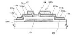
本実施の形態のボトムゲート構造の薄膜トランジスタを図10に示す。図10に示す薄膜
トランジスタには、基板100上にゲート電極層101が設けられ、ゲート電極層101
上にゲート絶縁層102が設けられ、ゲート絶縁層102上にソース電極層又はドレイン
電極層105a、105bが設けられ、ソース電極層又はドレイン電極層105a、10
5b上にバッファ層301a、301bが設けられ、ゲート絶縁層102、バッファ層3
01a、301b上に第1の酸化物半導体領域103が設けられ、第1の酸化物半導体領
域103上に第1の酸化物半導体領域103より導電率の低い第2の酸化物半導体領域1
04が設けられている。なお、第1の酸化物半導体領域103と第2の酸化物半導体領域
104は、同一の酸化物半導体層中に一緒に形成されてもよいし、異なる酸化物半導体層
として別々に形成されてもよい。また、第1の酸化物半導体領域103と第2の酸化物半
導体領域104の間に、導電率が段階的又は連続的に変化する酸化物半導体の中間領域が
存在してもよい。また、酸化物半導体中間領域は、第1の酸化物半導体領域103及び第
2の酸化物半導体領域104と、同一の酸化物半導体層中に一緒に形成されてもよいし、
異なる酸化物半導体層として別々に形成されてもよい。The thin film transistor having the bottom gate structure of the present embodiment is shown in FIG. In the thin film transistor shown in FIG. 10, a
A
The buffer layers 301a and 301b are provided on the 5b, and the
A first
04 is provided. The first
It may be formed separately as different oxide semiconductor layers.
また、ソース電極層又はドレイン電極層105a、105bは、第1の導電膜112a、
112b、第2の導電膜113a、113b、第3の導電膜114a、114bからなる
3層構造となっている。つまり、図10に示す薄膜トランジスタは、実施の形態1におい
て図1で示した薄膜トランジスタの第1の酸化物半導体領域103とソース電極層又はド
レイン電極層105a、105bとの間にバッファ層301a、301bを設けた構造の
薄膜トランジスタである。Further, the source electrode layer or the
It has a three-layer structure composed of 112b, the second
ソース領域又はドレイン領域として機能するバッファ層301a、301bには、実施の
形態1で示した第1の酸化物半導体領域103及び第2の酸化物半導体領域104を形成
する酸化物半導体を用いることができる。第1の酸化物半導体領域103及び第2の酸化
物半導体領域104と同様に、In、Ga、及びZnを含む酸化物半導体膜であるIn−
Ga−Zn−O系非単結晶膜を用いて形成するのが好ましい。ただし、バッファ層301
a、301bはn型の導電型を有し、その導電率は、第1の酸化物半導体領域103及び
第2の酸化物半導体領域104の導電率より高くなるようにする。例えば、バッファ層3
01a、301bの導電率は1.0×10⁻³S/cmより大きいことが好ましい。また
、バッファ層301a、301bにIn−Ga−Zn−O系非単結晶膜を用いる場合、少
なくともアモルファス成分を含んでいるものとし、非晶質構造の中に結晶粒(ナノクリス
タル)を含む場合もある。結晶粒(ナノクリスタル)は直径1nm〜10nm、代表的に
は2nm〜4nm程度である。For the
It is preferably formed using a Ga—Zn—O based non-single crystal film. However, the buffer layer 301
a and 301b have an n-type conductivity type, and the conductivity thereof is set to be higher than the conductivity of the first
The conductivity of 01a and 301b is preferably greater than 1.0 × 10⁻³ S / cm. When an In-Ga-Zn-O non-single crystal film is used for the
バッファ層301a、301bに用いる酸化物半導体膜は、スパッタ法で成膜する。酸化
物半導体膜の具体的な成膜条件例としては、直径8インチのIn、Ga、及びZnを含む
酸化物半導体ターゲット(In2O3:Ga2O3:ZnO=1:1:1)を用いて、基
板とターゲットの間との距離を170mm、圧力0.4Pa、直流(DC)電源0.5k
W、成膜ガスAr:O2=50:1(sccm)、成膜温度を室温としてスパッタ成膜を
行う。なお、上記結晶粒(ナノクリスタル)は、ターゲットの成分比、成膜圧力(0.1
Pa〜2.0Pa)、電力(250W〜3000W:8インチφ)、温度(室温〜100
℃)、反応性スパッタの成膜条件などを適宜調節することで、結晶粒の有無や、結晶粒の
密度や、直径サイズを調節することができる。The oxide semiconductor film used for the
Sputter film formation is performed with W, the film formation gas Ar: O2 = 50: 1 (sccm), and the film formation temperature at room temperature. The crystal grains (nanocrystals) are the target component ratio and the film formation pressure (0.1).
Pa to 2.0 Pa), electric power (250 W to 3000 W: 8 inch φ), temperature (room temperature to 100)
The presence or absence of crystal grains, the density of crystal grains, and the diameter size can be adjusted by appropriately adjusting the film formation conditions of the reactive sputter (° C.).
ただし、バッファ層301a、301bに用いる酸化物半導体膜は、第1の酸化物半導体
領域103及び第2の酸化物半導体領域104に用いる酸化物半導体膜の成膜条件と異な
らせる。第1の酸化物半導体領域103及び第2の酸化物半導体領域104に用いる酸化
物半導体膜の成膜条件における酸素ガス流量の比率よりも、バッファ層301a、301
bに用いる酸化物半導体膜の成膜条件における酸素ガス流量の比率を少なくする。例えば
、バッファ層301a、301bに用いる酸化物半導体膜の成膜条件は、成膜ガス全体に
対する酸素ガスの比率を10体積%未満とするのが好ましい。また、バッファ層301a
、301bに用いる酸化物半導体膜の成膜条件は、成膜ガスに酸素ガスを含まない、アル
ゴンなどの希ガス雰囲気下としてもよい。However, the oxide semiconductor film used for the
Reduce the ratio of oxygen gas flow rate under the film formation conditions of the oxide semiconductor film used for b. For example, the film forming conditions of the oxide semiconductor film used for the
The film forming condition of the oxide semiconductor film used in 301b may be a rare gas atmosphere such as argon, which does not contain oxygen gas in the film forming gas.
バッファ層301a、301bに用いる酸化物半導体膜の膜厚は、5nm〜20nmとす
る。勿論、膜中に結晶粒が含まれる場合、含まれる結晶粒のサイズが膜厚を超える大きさ
とならない。本実施の形態では、バッファ層301a、301bに用いる酸化物半導体膜
の膜厚は、5nmとする。The film thickness of the oxide semiconductor film used for the
また、バッファ層301a、301bにn型を付与する不純物元素を含ませてもよい。不
純物元素として、例えばマグネシウム、アルミニウム、チタン、鉄、錫、カルシウム、ゲ
ルマニウム、スカンジウム、イットリウム、ジルコニウム、ハフニウム、ボロン、タリウ
ム、鉛などを用いることができる。マグネシウム、アルミニウム、チタンなどをバッファ
層に含ませると、酸素のブロッキング効果などがあり、成膜後の加熱処理などによって酸
化物半導体層の酸素濃度を最適な範囲内に保持できる。Further, the
また、バッファ層のキャリア濃度範囲は、1×10¹⁸/cm3以上(1×1022/c
m3以下)が好ましい。The carrier concentration range of the buffer layer is 1 × 10¹⁸ / cm3 or more (1 × 10²² / c).
m3 or less) is preferable.
以上のように、バッファ層301a、301bを設けることにより、第1の酸化物半導体
領域103と、ソース電極層又はドレイン電極層105a、105bとの間で、ショット
キー接合よりも熱的安定性を向上させることができ、薄膜トランジスタの動作特性を安定
させることができる。また、導電性がよいので高いドレイン電圧でも良好な移動度を保持
することができる。As described above, by providing the
なお、本実施の形態の薄膜トランジスタのバッファ層301a、301b以外の構造と材
料については、実施の形態1を参照されたい。For structures and materials other than the
本実施の形態の薄膜トランジスタの作製工程は、実施の形態2で示した薄膜トランジスタ
の作製工程とほぼ同様である。まず、実施の形態2で示した方法で、第1の導電膜112
〜第3の導電膜114まで成膜し、連続してバッファ層301a、301bを形成するた
めの酸化物半導体膜302を、上記の方法を用いてスパッタ成膜する(図11(A)参照
)。次に、第3のフォトリソグラフィ工程によって、第1の導電膜112〜第3の導電膜
114と同時に酸化物半導体膜302を島状にエッチングして、ソース電極層又はドレイ
ン電極層105a、105b及び酸化物半導体膜302a、302bを形成し、実施の形
態2と同様の方法で逆スパッタを行う(図11(B)参照)。それから、実施の形態2で
示した方法で第1の酸化物半導体領域103及び第2の酸化物半導体領域104を形成す
る際に、同時に酸化物半導体膜302a、302bもエッチングし、バッファ層301a
、301bを形成する(図11(C)参照)。以降の工程は実施の形態2と同様である。The manufacturing process of the thin film transistor of the present embodiment is substantially the same as the manufacturing process of the thin film transistor shown in the second embodiment. First, by the method shown in the second embodiment, the first
A film is formed up to the third
, 301b (see FIG. 11C). Subsequent steps are the same as in the second embodiment.
なお、本実施の形態に示す構成は、他の実施の形態に示した構成を適宜組み合わせて用い
ることができることとする。It should be noted that the configuration shown in this embodiment can be used in combination with the configurations shown in other embodiments as appropriate.
(実施の形態4)
本実施の形態では、実施の形態1及び実施の形態3で示した薄膜トランジスタとは異なる
形状の薄膜トランジスタについて図30を用いて説明する。(Embodiment 4)
In the present embodiment, a thin film transistor having a shape different from that shown in the first and third embodiments will be described with reference to FIG.
本実施の形態のボトムゲート構造の薄膜トランジスタを図30(A)及び図30(B)に
示す。図30(A)及び図30(B)に示す薄膜トランジスタは、基板100上にゲート
電極層101が設けられ、ゲート電極層101上にゲート絶縁層102が設けられ、ゲー
ト絶縁層102上にソース電極層又はドレイン電極層105a、105bが設けられ、ゲ
ート絶縁層102、ソース電極層又はドレイン電極層105a、105b上に第1の酸化
物半導体領域103が設けられ、第1の酸化物半導体領域103上に第1の酸化物半導体
領域103より導電率の低い第2の酸化物半導体領域104が設けられている。なお、第
1の酸化物半導体領域103と第2の酸化物半導体領域104は、同一の酸化物半導体層
中に一緒に形成されてもよいし、異なる酸化物半導体層として別々に形成されてもよい。
また、第1の酸化物半導体領域103と第2の酸化物半導体領域104の間に、導電率が
段階的又は連続的に変化する酸化物半導体の中間領域が存在してもよい。また、酸化物半
導体中間領域は、第1の酸化物半導体領域103及び第2の酸化物半導体領域104と、
同一の酸化物半導体層中に一緒に形成されてもよいし、異なる酸化物半導体層として別々
に形成されてもよい。The thin film transistors having the bottom gate structure of this embodiment are shown in FIGS. 30 (A) and 30 (B). In the thin film transistors shown in FIGS. 30A and 30B, a
Further, an intermediate region of the oxide semiconductor in which the conductivity changes stepwise or continuously may exist between the first
It may be formed together in the same oxide semiconductor layer, or may be formed separately as different oxide semiconductor layers.
また、ソース電極層又はドレイン電極層105a、105bは、第1の導電膜112a、
112b、第2の導電膜113a、113b、第3の導電膜114a、114bからなる
3層構造となっている。また、ソース電極層又はドレイン電極層105a、105bの側
面には絶縁層が設けられている。図30(A)では、ソース電極層又はドレイン電極層1
05a、105bの側面に酸化膜403a、403bが形成され、図30(B)では、ソ
ース電極層又はドレイン電極層105a、105bの側面にサイドウォール絶縁層404
a、404bが形成されている。Further, the source electrode layer or the
It has a three-layer structure composed of 112b, the second
a and 404b are formed.
つまり、図30(A)に示す薄膜トランジスタは、実施の形態1において図1で示した薄
膜トランジスタの第1の酸化物半導体領域103の一部がソース電極層又はドレイン電極
層105a、105bの側面部と酸化膜403a、403bを介して接する構造となって
いる。図30(B)に示す薄膜トランジスタは、実施の形態1において図1で示した薄膜
トランジスタの第1の酸化物半導体領域103の一部がソース電極層又はドレイン電極層
105a、105bの側面部とサイドウォール絶縁層404a、404bを介して接する
構造となっている。That is, in the thin film transistor shown in FIG. 30A, a part of the first
図30(A)に示す酸化膜403a、403bは、ソース電極層又はドレイン電極層10
5a、105bの側面を酸化して形成したものである。酸化方法としては、熱酸化、酸素
プラズマ処理またはオゾン水洗浄などを行うのが好ましい。具体的には、実施の形態2の
図2(C)に示すソース電極層又はドレイン電極層105a、105bを形成し、レジス
トマスク131を残した状態で、熱酸化、プラズマ酸化またはオゾン水処理を施すことに
よって、ソース電極層又はドレイン電極層105a、105bの側面を酸化して酸化膜4
03a、403bを形成することが好ましい。ただし、ソース電極層又はドレイン電極層
105a、105bが異なる導電膜の積層構造である場合、酸化膜403a、403bも
異なる酸化膜の積層構造となる。例えば、第1の導電膜112a、112b、第3の導電
膜114a、114bとしてチタンを、第2の導電膜113a、113bとしてネオジム
を含むアルミニウム合金を用いた場合、酸化膜403a、403bは、上層から順番に酸
化チタン膜、ネオジムを含む酸化アルミニウム合金膜、酸化チタン膜の3層積層構造とな
る。なお、酸化膜403a、403bの導電率は、第1の酸化物半導体領域103より小
さいものとする。The
It is formed by oxidizing the side surfaces of 5a and 105b. As the oxidation method, thermal oxidation, oxygen plasma treatment, ozone water washing and the like are preferable. Specifically, the source electrode layer or
It is preferable to form 03a and 403b. However, when the source electrode layer or the
図30(B)に示すサイドウォール絶縁層404a、404bは、シリコン膜、酸化シリ
コン膜、窒化酸化シリコン膜または酸化窒化シリコン膜で形成される。具体的には、実施
の形態2の図2(C)に示すソース電極層又はドレイン電極層105a、105bを形成
し、レジストマスク131を除去した後、プラズマCVD法やスパッタリング法などによ
り、シリコン膜、酸化シリコン膜、窒化酸化シリコン膜または酸化窒化シリコン膜を、ソ
ース電極層又はドレイン電極層105a、105bを覆うように成膜する。それから、垂
直方向を主体とした異方性エッチングを行うことで、新たに形成されたシリコン膜、酸化
シリコン膜、窒化酸化シリコン膜または酸化窒化シリコン膜を部分的にエッチングし、ソ
ース電極層又はドレイン電極層105a、105bの側面に接するサイドウォール絶縁層
404a、404bを形成することができる。このとき異方性エッチングとしては、ドラ
イエッチングが好ましく、エッチングガスとしては、CHF3とヘリウムの混合ガスを用
いることができる。ただし、サイドウォール絶縁層として、ゲート絶縁層と同じ種類のシ
リコン膜を用いる場合、エッチングの選択比をとることができないので、上記異方性エッ
チングにより、ゲート絶縁層102もエッチングされる場合がある。The
図30(A)及び図30(B)に示すように、酸化膜403a、403bまたはサイドウ
ォール絶縁層404a、404bをソース電極層又はドレイン電極層105a、105b
の側面に形成することによって、ドレイン電流の経路を、ソース電極層又はドレイン電極
層105a、105bを結ぶ直線状の経路ではなく、酸化膜403a、403bまたはサ
イドウォール絶縁層404a、404bを迂回する経路にすることができる。これにより
、薄膜トランジスタがオフのときに流れるオフ電流を低減することができる。また、これ
は、第2の酸化物半導体領域104が設けられる構成に限定されるものではなく、第2の
酸化物半導体領域104が設けられていない、活性層が単一の酸化物半導体層である構造
の薄膜トランジスタであっても、ソース電極層又はドレイン電極層105a、105bの
側面に酸化膜403a、403bまたはサイドウォール絶縁層404a、404bを設け
ることによって同様の効果を得ることができる。As shown in FIGS. 30A and 30B, the
By forming on the side surface of, the drain current path is not a linear path connecting the source electrode layer or the
また、ソース電極層又はドレイン電極層105a、105bの側面に、酸化膜403a、
403bまたはサイドウォール絶縁層404a、404bを設けることによって、第1の
酸化物半導体領域103の被覆性を向上し、段差形状による第1の酸化物半導体領域10
3の段切れを防ぐことができる。Further, on the side surfaces of the source electrode layer or the
By providing the 403b or the
It is possible to prevent the step breakage of 3.
また、本実施の形態でも、実施の形態3で示したように、第1の酸化物半導体領域103
とソース電極層又はドレイン電極層105a、105bとの間にバッファ層を設けた構造
としてもよい。Further, also in the present embodiment, as shown in the third embodiment, the first
A buffer layer may be provided between the source electrode layer and the
なお、本実施の形態の酸化膜403a、403b及びサイドウォール絶縁層404a、4
04b以外の構造と材料については、実施の形態1を参照されたい。The
For structures and materials other than 04b, see
なお、本実施の形態に示す構成は、他の実施の形態に示した構成を適宜組み合わせて用い
ることができることとする。It should be noted that the configuration shown in this embodiment can be used in combination with the configurations shown in other embodiments as appropriate.
(実施の形態5)
本実施の形態では、半導体装置の一例である表示装置において、同一基板上に少なくとも
駆動回路の一部と、画素部に配置する薄膜トランジスタを作製する例について以下に説明
する。(Embodiment 5)
In the present embodiment, in a display device which is an example of a semiconductor device, an example of manufacturing at least a part of a drive circuit and a thin film transistor to be arranged in a pixel portion on the same substrate will be described below.
画素部に配置する薄膜トランジスタは、実施の形態1乃至実施の形態4に従って形成する
。また、実施の形態1乃至実施の形態4に示す薄膜トランジスタはnチャネル型TFTで
あるため、駆動回路のうち、nチャネル型TFTで構成することができる駆動回路の一部
を画素部の薄膜トランジスタと同一基板上に形成する。The thin film transistor to be arranged in the pixel portion is formed according to the first to fourth embodiments. Further, since the thin film transistors shown in the first to fourth embodiments are n-channel TFTs, a part of the drive circuit that can be configured by the n-channel TFTs is the same as the thin film transistor of the pixel portion. Formed on the substrate.
半導体装置の一例であるアクティブマトリクス型液晶表示装置のブロック図の一例を図1
4(A)に示す。図14(A)に示す表示装置は、基板5300上に表示素子を備えた画
素を複数有する画素部5301と、各画素を選択する走査線駆動回路5302と、選択さ
れた画素へのビデオ信号の入力を制御する信号線駆動回路5303とを有する。FIG. 1 is an example of a block diagram of an active matrix type liquid crystal display device which is an example of a semiconductor device.
It is shown in 4 (A). The display device shown in FIG. 14 (A) includes a pixel unit 5301 having a plurality of pixels having a display element on the
画素部5301は、信号線駆動回路5303から列方向に伸張して配置された複数の信号
線S1〜Sm(図示せず。)により信号線駆動回路5303と接続され、走査線駆動回路
5302から行方向に伸張して配置された複数の走査線G1〜Gn(図示せず。)により
走査線駆動回路5302と接続され、信号線S1〜Sm並びに走査線G1〜Gnに対応し
てマトリクス状に配置された複数の画素(図示せず。)を有する。そして、各画素は、信
号線Sj(信号線S1〜Smのうちいずれか一)、走査線Gi(走査線G1〜Gnのうち
いずれか一)と接続される。The pixel unit 5301 is connected to the signal line drive circuit 5303 by a plurality of signal lines S1 to Sm (not shown) arranged so as to extend in the column direction from the signal line drive circuit 5303, and runs from the scanning
また、実施の形態1乃至実施の形態4に示す薄膜トランジスタは、nチャネル型TFTで
あり、nチャネル型TFTで構成する信号線駆動回路について図15を用いて説明する。Further, the thin film transistors shown in the first to fourth embodiments are n-channel type TFTs, and a signal line drive circuit composed of the n-channel type TFTs will be described with reference to FIG.
図15に示す信号線駆動回路は、ドライバIC5601、スイッチ群5602_1〜56
02_M、第1の配線5611、第2の配線5612、第3の配線5613及び配線56
21_1〜5621_Mを有する。スイッチ群5602_1〜5602_Mそれぞれは、
第1の薄膜トランジスタ5603a、第2の薄膜トランジスタ5603b及び第3の薄膜
トランジスタ5603cを有する。The signal line drive circuit shown in FIG. 15 includes a driver IC5601 and a switch group 5602_1 to 56.
02_M,
It has 21_1 to 5621_M. Switch groups 5602_1 to 5602_M respectively
It has a first
ドライバIC5601は第1の配線5611、第2の配線5612、第3の配線5613
及び配線5621_1〜5621_Mに接続される。そして、スイッチ群5602_1〜
5602_Mそれぞれは、第1の配線5611、第2の配線5612、第3の配線561
3及びスイッチ群5602_1〜5602_Mそれぞれに対応した配線5621_1〜5
621_Mに接続される。そして、配線5621_1〜5621_Mそれぞれは、第1の
薄膜トランジスタ5603a、第2の薄膜トランジスタ5603b及び第3の薄膜トラン
ジスタ5603cを介して、3つの信号線(信号線Sm−2、信号線Sm−1、信号線S
m(m=3M))に接続される。例えば、J列目の配線5621_J(配線5621_1
〜配線5621_Mのうちいずれか一)は、スイッチ群5602_Jが有する第1の薄膜
トランジスタ5603a、第2の薄膜トランジスタ5603b及び第3の薄膜トランジス
タ5603cを介して、信号線Sj−2、信号線Sj―1、信号線Sj(j=3J)に接
続される。The driver IC5601 has a
And wiring 5621_1 to 5621_M. And the switch group 5602_1-1
5602_M Each is the
Wiring 5621_1-5 corresponding to 3 and switch group 5602_1 to 5602_M respectively
Connected to 621_M. Each of the wirings 5621_1 to 5621_M has three signal lines (signal line Sm-2, signal line Sm-1, signal line S) via the first
It is connected to m (m = 3M)). For example, wiring 5621_J in the Jth row (wiring 5621_1)
~ Wiring 5621_M) is a signal line Sj-2, a signal line Sj-1, and a signal via the first
なお、第1の配線5611、第2の配線5612、第3の配線5613には、それぞれ信
号が入力される。Signals are input to the
なお、ドライバIC5601は、単結晶半導体を用いて形成されていることが望ましい。
さらに、スイッチ群5602_1〜5602_Mは、画素部と同一基板上に形成されてい
ることが望ましい。したがって、ドライバIC5601とスイッチ群5602_1〜56
02_MとはFPCなどを介して接続するとよい。又は画素部と同一の基板上に貼り合わ
せなどによって、単結晶半導体層を設け、ドライバIC5601を形成してもよい。It is desirable that the driver IC5601 is formed by using a single crystal semiconductor.
Further, it is desirable that the switch groups 5602_1 to 5602_M are formed on the same substrate as the pixel portion. Therefore, the driver IC5601 and the switch group 5602_1 to 56
It is preferable to connect to 02_M via FPC or the like. Alternatively, the driver IC5601 may be formed by providing a single crystal semiconductor layer by laminating or the like on the same substrate as the pixel portion.
次に、図15に示した信号線駆動回路の動作について、図16のタイミングチャートを参
照して説明する。なお、図16のタイミングチャートは、i行目の走査線Giが選択され
ている場合のタイミングチャートを示している。さらに、i行目の走査線Giの選択期間
は、第1のサブ選択期間T1、第2のサブ選択期間T2及び第3のサブ選択期間T3に分
割されている。さらに、図15の信号線駆動回路は、他の行の走査線が選択されている場
合でも図16と同様の動作をする。Next, the operation of the signal line drive circuit shown in FIG. 15 will be described with reference to the timing chart of FIG. The timing chart of FIG. 16 shows a timing chart when the scanning line Gi on the i-th row is selected. Further, the selection period of the scanning line Gi on the i-th row is divided into a first sub-selection period T1, a second sub-selection period T2, and a third sub-selection period T3. Further, the signal line drive circuit of FIG. 15 operates in the same manner as in FIG. 16 even when scanning lines of other lines are selected.
なお、図16のタイミングチャートは、J列目の配線5621_Jが第1の薄膜トランジ
スタ5603a、第2の薄膜トランジスタ5603b及び第3の薄膜トランジスタ560
3cを介して、信号線Sj−2、信号線Sj―1、信号線Sjに接続される場合について
示している。In the timing chart of FIG. 16, the wiring 5621_J in the Jth column is the first
The case where it is connected to the signal line Sj-2, the signal line Sj-1, and the signal line Sj via 3c is shown.
なお、図16のタイミングチャートは、i行目の走査線Giが選択されるタイミング、第
1の薄膜トランジスタ5603aのオン・オフのタイミング5703a、第2の薄膜トラ
ンジスタ5603bのオン・オフのタイミング5703b、第3の薄膜トランジスタ56
03cのオン・オフのタイミング5703c及びJ列目の配線5621_Jに入力される
信号5721_Jを示している。In the timing chart of FIG. 16, the timing at which the scanning line Gi on the i-th row is selected, the on / off timing 5703a of the first
The on / off timing 5703c of 03c and the signal 5721_J input to the wiring 5621_J in the Jth row are shown.
なお、配線5621_1〜配線5621_Mには第1のサブ選択期間T1、第2のサブ選
択期間T2及び第3のサブ選択期間T3において、それぞれ別のビデオ信号が入力される
。例えば、第1のサブ選択期間T1において配線5621_Jに入力されるビデオ信号は
信号線Sj−2に入力され、第2のサブ選択期間T2において配線5621_Jに入力さ
れるビデオ信号は信号線Sj―1に入力され、第3のサブ選択期間T3において配線56
21_Jに入力されるビデオ信号は信号線Sjに入力される。さらに、第1のサブ選択期
間T1、第2のサブ選択期間T2及び第3のサブ選択期間T3において、配線5621_
Jに入力されるビデオ信号をそれぞれData_j−2、Data_j―1、Data_
jとする。Note that different video signals are input to the wirings 5621_1 to 5621_M in the first subselection period T1, the second subselection period T2, and the third subselection period T3. For example, the video signal input to the wiring 5621_J in the first sub-selection period T1 is input to the signal line Sj-2, and the video signal input to the wiring 5621_J in the second sub-selection period T2 is the signal line Sj-1. Is input to, and wiring 56 in the third sub-selection period T3.
The video signal input to 21_J is input to the signal line Sj. Further, in the first subselection period T1, the second subselection period T2, and the third subselection period T3, the wiring 5621_
The video signals input to J are Data_j-2, Data_j-1, and Data_, respectively.
Let j.
図16に示すように、第1のサブ選択期間T1において第1の薄膜トランジスタ5603
aがオンし、第2の薄膜トランジスタ5603b及び第3の薄膜トランジスタ5603c
がオフする。このとき、配線5621_Jに入力されるData_j−2が、第1の薄膜
トランジスタ5603aを介して信号線Sj−2に入力される。第2のサブ選択期間T2
では、第2の薄膜トランジスタ5603bがオンし、第1の薄膜トランジスタ5603a
及び第3の薄膜トランジスタ5603cがオフする。このとき、配線5621_Jに入力
されるData_j―1が、第2の薄膜トランジスタ5603bを介して信号線Sj―1
に入力される。第3のサブ選択期間T3では、第3の薄膜トランジスタ5603cがオン
し、第1の薄膜トランジスタ5603a及び第2の薄膜トランジスタ5603bがオフす
る。このとき、配線5621_Jに入力されるData_jが、第3の薄膜トランジスタ
5603cを介して信号線Sjに入力される。As shown in FIG. 16, the first thin film transistor 5603 during the first subselection period T1.
When a is turned on, the second
Turns off. At this time, Data_j-2 input to the wiring 5621_J is input to the signal line Sj-2 via the first
Then, the second
And the third
Is entered in. In the third subselection period T3, the third
以上のことから、図15の信号線駆動回路は、1ゲート選択期間を3つに分割することで
、1ゲート選択期間中に1つの配線5621から3つの信号線にビデオ信号を入力するこ
とができる。したがって、図15の信号線駆動回路は、ドライバIC5601が形成され
る基板と、画素部が形成されている基板との接続数を信号線の数に比べて約1/3にする
ことができる。接続数が約1/3になることによって、図15の信号線駆動回路は、信頼
性、歩留まりなどを向上できる。From the above, the signal line drive circuit of FIG. 15 can input a video signal from one wiring 5621 to three signal lines during one gate selection period by dividing one gate selection period into three. it can. Therefore, in the signal line drive circuit of FIG. 15, the number of connections between the substrate on which the driver IC5601 is formed and the substrate on which the pixel portion is formed can be reduced to about 1/3 of the number of signal lines. By reducing the number of connections to about 1/3, the signal line drive circuit of FIG. 15 can improve reliability, yield, and the like.
なお、図15のように、1ゲート選択期間を複数のサブ選択期間に分割し、複数のサブ選
択期間それぞれにおいて、ある1つの配線から複数の信号線それぞれにビデオ信号を入力
することができれば、薄膜トランジスタの配置や数、駆動方法などは限定されない。As shown in FIG. 15, if one gate selection period can be divided into a plurality of sub-selection periods and a video signal can be input to each of a plurality of signal lines from a certain wiring in each of the plurality of sub-selection periods. The arrangement and number of thin film transistors and the driving method are not limited.
例えば、3つ以上のサブ選択期間それぞれにおいて1つの配線から3つ以上の信号線それ
ぞれにビデオ信号を入力する場合は、薄膜トランジスタ及び薄膜トランジスタを制御する
ための配線を追加すればよい。ただし、1ゲート選択期間を4つ以上のサブ選択期間に分
割すると、1つのサブ選択期間が短くなる。したがって、1ゲート選択期間は、2つ又は
3つのサブ選択期間に分割されることが望ましい。For example, when a video signal is input from one wiring to each of the three or more signal lines in each of the three or more sub-selection periods, the thin film transistor and the wiring for controlling the thin film transistor may be added. However, if one gate selection period is divided into four or more sub-selection periods, one sub-selection period becomes shorter. Therefore, it is desirable that the one-gate selection period be divided into two or three sub-selection periods.
別の例として、図17のタイミングチャートに示すように、1つの選択期間をプリチャー
ジ期間Tp、第1のサブ選択期間T1、第2のサブ選択期間T2、第3の選択期間T3に
分割してもよい。さらに、図17のタイミングチャートは、i行目の走査線Giが選択さ
れるタイミング、第1の薄膜トランジスタ5603aのオン・オフのタイミング5803
a、第2の薄膜トランジスタ5603bのオン・オフのタイミング5803b、第3の薄
膜トランジスタ5603cのオン・オフのタイミング5803c及びJ列目の配線562
1_Jに入力される信号5821_Jを示している。図17に示すように、プリチャージ
期間Tpにおいて第1の薄膜トランジスタ5603a、第2の薄膜トランジスタ5603
b及び第3の薄膜トランジスタ5603cがオンする。このとき、配線5621_Jに入
力されるプリチャージ電圧Vpが第1の薄膜トランジスタ5603a、第2の薄膜トラン
ジスタ5603b及び第3の薄膜トランジスタ5603cを介してそれぞれ信号線Sj−
2、信号線Sj―1、信号線Sjに入力される。第1のサブ選択期間T1において第1の
薄膜トランジスタ5603aがオンし、第2の薄膜トランジスタ5603b及び第3の薄
膜トランジスタ5603cがオフする。このとき、配線5621_Jに入力されるDat
a_j−2が、第1の薄膜トランジスタ5603aを介して信号線Sj−2に入力される
。第2のサブ選択期間T2では、第2の薄膜トランジスタ5603bがオンし、第1の薄
膜トランジスタ5603a及び第3の薄膜トランジスタ5603cがオフする。このとき
、配線5621_Jに入力されるData_j―1が、第2の薄膜トランジスタ5603
bを介して信号線Sj―1に入力される。第3のサブ選択期間T3では、第3の薄膜トラ
ンジスタ5603cがオンし、第1の薄膜トランジスタ5603a及び第2の薄膜トラン
ジスタ5603bがオフする。このとき、配線5621_Jに入力されるData_jが
、第3の薄膜トランジスタ5603cを介して信号線Sjに入力される。As another example, as shown in the timing chart of FIG. 17, one selection period is divided into a precharge period Tp, a first sub-selection period T1, a second sub-selection period T2, and a third selection period T3. You may. Further, in the timing chart of FIG. 17, the timing at which the scanning line Gi on the i-th row is selected and the on / off timing of the first
a, On / off timing of the second
The signal 5821_J input to 1_J is shown. As shown in FIG. 17, the first
b and the third
2. Input to signal line Sj-1 and signal line Sj. In the first subselection period T1, the first
a_j-2 is input to the signal line Sj-2 via the first
It is input to the signal line Sj-1 via b. In the third subselection period T3, the third
以上のことから、図17のタイミングチャートを適用した図15の信号線駆動回路は、サ
ブ選択期間の前にプリチャージ選択期間を設けることによって、信号線をプリチャージで
きるため、画素へのビデオ信号の書き込みを高速に行うことができる。なお、図17にお
いて、図16と同様なものに関しては共通の符号を用いて示し、同一部分又は同様な機能
を有する部分の詳細な説明は省略する。From the above, the signal line drive circuit of FIG. 15 to which the timing chart of FIG. 17 is applied can precharge the signal line by providing the precharge selection period before the sub-selection period, so that the video signal to the pixel can be obtained. Can be written at high speed. In FIG. 17, the same parts as those in FIG. 16 are shown by using common reference numerals, and detailed description of the same parts or parts having the same functions will be omitted.
また、走査線駆動回路の構成について説明する。走査線駆動回路は、シフトレジスタ、バ
ッファを有している。また場合によってはレベルシフタを有していても良い。走査線駆動
回路において、シフトレジスタにクロック信号(CLK)及びスタートパルス信号(SP
)が入力されることによって、選択信号が生成される。生成された選択信号はバッファに
おいて緩衝増幅され、対応する走査線に供給される。走査線には、1ライン分の画素のト
ランジスタのゲート電極が接続されている。そして、1ライン分の画素のトランジスタを
一斉にONにしなくてはならないので、バッファは大きな電流を流すことが可能なものが
用いられる。Further, the configuration of the scanning line drive circuit will be described. The scanning line drive circuit has a shift register and a buffer. In some cases, it may have a level shifter. In the scanning line drive circuit, the clock signal (CLK) and start pulse signal (SP) are stored in the shift register.
) Is input to generate a selection signal. The generated selection signal is buffer amplified in the buffer and fed to the corresponding scan line. The gate electrode of the transistor of one line of pixels is connected to the scanning line. Then, since the transistors of one line of pixels must be turned on all at once, a buffer capable of passing a large current is used.
走査線駆動回路の一部に用いるシフトレジスタの一形態について図18及び図19を用い
て説明する。A form of a shift register used as a part of the scanning line drive circuit will be described with reference to FIGS. 18 and 19.
図18にシフトレジスタの回路構成を示す。図18に示すシフトレジスタは、フリップフ
ロップ5701_1〜5701_nという複数のフリップフロップで構成される。また、
第1のクロック信号、第2のクロック信号、スタートパルス信号、リセット信号が入力さ
れて動作する。FIG. 18 shows the circuit configuration of the shift register. The shift register shown in FIG. 18 is composed of a plurality of flip-flops called flip-flops 5701_1 to 5701_n. Also,
The first clock signal, the second clock signal, the start pulse signal, and the reset signal are input to operate.
図18のシフトレジスタの接続関係について説明する。1段目のフリップフロップ570
1_1は、第1の配線5711、第2の配線5712、第4の配線5714、第5の配線
5715、第7の配線5717_1、及び第7の配線5717_2と接続される。また、
2段目のフリップフロップ5701_2は、第3の配線5713、第4の配線5714、
第5の配線5715、第7の配線5717_1、第7の配線5717_2及び第7の配線
5717_3と接続される。The connection relationship of the shift register of FIG. 18 will be described. 1st stage flip-flop 570
1_1 is connected to the
The second-stage flip-flop 5701_2 has a
It is connected to the
同様に、i段目のフリップフロップ5701_i(フリップフロップ5701_1〜57
01_nのうちいずれか一)は、第2の配線5712又は第3の配線5713の一方、第
4の配線5714、第5の配線5715、第7の配線5717_i−1、第7の配線57
17_i、及び第7の配線5717_i+1と接続される。ここで、iが奇数の場合には
、i段目のフリップフロップ5701_iは第2の配線5712と接続され、iが偶数で
ある場合には、i段目のフリップフロップ5701_iは第3の配線5713と接続され
ることになる。Similarly, the i-stage flip-flop 5701_i (flip-flop 5701_1 to 57)
Any one of 01_n) is one of the
It is connected to 17_i and the seventh
また、n段目のフリップフロップ5701_nは、第2の配線5712又は第3の配線5
713の一方、第4の配線5714、第5の配線5715、第7の配線5717_n−1
、第7の配線5717_n、及び第6の配線5716と接続される。Further, the n-th stage flip-flop 5701_n is the
On the other hand of 713, the
, 7th wiring 5717_n, and
なお、第1の配線5711、第2の配線5712、第3の配線5713、第6の配線57
16を、それぞれ第1の信号線、第2の信号線、第3の信号線、第4の信号線と呼んでも
よい。さらに、第4の配線5714、第5の配線5715を、それぞれ第1の電源線、第
2の電源線と呼んでもよい。The
16 may be referred to as a first signal line, a second signal line, a third signal line, and a fourth signal line, respectively. Further, the
次に、図18に示すフリップフロップの詳細について、図19を用いて説明する。図19
に示すフリップフロップは、第1の薄膜トランジスタ5571、第2の薄膜トランジスタ
5572、第3の薄膜トランジスタ5573、第4の薄膜トランジスタ5574、第5の
薄膜トランジスタ5575、第6の薄膜トランジスタ5576、第7の薄膜トランジスタ
5577及び第8の薄膜トランジスタ5578を有する。なお、第1の薄膜トランジスタ
5571、第2の薄膜トランジスタ5572、第3の薄膜トランジスタ5573、第4の
薄膜トランジスタ5574、第5の薄膜トランジスタ5575、第6の薄膜トランジスタ
5576、第7の薄膜トランジスタ5577及び第8の薄膜トランジスタ5578は、n
チャネル型トランジスタであり、ゲート・ソース間電圧(Vgs)がしきい値電圧(Vt
h)を上回ったとき導通状態になるものとする。Next, the details of the flip-flop shown in FIG. 18 will be described with reference to FIG. FIG. 19
The flip-flops shown in the above are the first
It is a channel type transistor, and the gate-source voltage (Vgs) is the threshold voltage (Vt).
When it exceeds h), it shall be in a conductive state.
また、図19に示すフリップフロップは、第1の配線5501、第2の配線5502、第
3の配線5503、第4の配線5504、第5の配線5505、及び第6の配線5506
を有する。Further, the flip-flop shown in FIG. 19 has a first wiring 5501, a
Have.
ここでは全ての薄膜トランジスタは、エンハンスメント型のnチャネル型トランジスタと
する例を示すが、特に限定されず、例えば、デプレッション型のnチャネル型トランジス
タを用いても駆動回路を駆動させることもできる。Here, an example in which all the thin film transistors are enhancement type n-channel transistors are shown, but the present invention is not particularly limited, and for example, a drive circuit can be driven by using a depletion-type n-channel transistors.
次に、図18に示すフリップフロップの接続構成について、以下に示す。Next, the connection configuration of the flip-flop shown in FIG. 18 is shown below.
第1の薄膜トランジスタ5571の第1の電極(ソース電極またはドレイン電極の一方)
が第4の配線5504に接続され、第1の薄膜トランジスタ5571の第2の電極(ソー
ス電極またはドレイン電極の他方)が第3の配線5503に接続される。The first electrode of the first thin film transistor 5571 (either the source electrode or the drain electrode)
Is connected to the
第2の薄膜トランジスタ5572の第1の電極が第6の配線5506に接続され、第2の
薄膜トランジスタ5572の第2の電極が第3の配線5503に接続される。The first electrode of the second
第3の薄膜トランジスタ5573の第1の電極が第5の配線5505に接続され、第3の
薄膜トランジスタ5573の第2の電極が第2の薄膜トランジスタ5572のゲート電極
に接続され、第3の薄膜トランジスタ5573のゲート電極が第5の配線5505に接続
される。The first electrode of the third
第4の薄膜トランジスタ5574の第1の電極が第6の配線5506に接続され、第4の
薄膜トランジスタ5574の第2の電極が第2の薄膜トランジスタ5572のゲート電極
に接続され、第4の薄膜トランジスタ5574のゲート電極が第1の薄膜トランジスタ5
571のゲート電極に接続される。The first electrode of the fourth
It is connected to the gate electrode of 571.
第5の薄膜トランジスタ5575の第1の電極が第5の配線5505に接続され、第5の
薄膜トランジスタ5575の第2の電極が第1の薄膜トランジスタ5571のゲート電極
に接続され、第5の薄膜トランジスタ5575のゲート電極が第1の配線5501に接続
される。The first electrode of the fifth
第6の薄膜トランジスタ5576の第1の電極が第6の配線5506に接続され、第6の
薄膜トランジスタ5576の第2の電極が第1の薄膜トランジスタ5571のゲート電極
に接続され、第6の薄膜トランジスタ5576のゲート電極が第2の薄膜トランジスタ5
572のゲート電極に接続される。The first electrode of the sixth
It is connected to the gate electrode of 572.
第7の薄膜トランジスタ5577の第1の電極が第6の配線5506に接続され、第7の
薄膜トランジスタ5577の第2の電極が第1の薄膜トランジスタ5571のゲート電極
に接続され、第7の薄膜トランジスタ5577のゲート電極が第2の配線5502に接続
される。第8の薄膜トランジスタ5578の第1の電極が第6の配線5506に接続され
、第8の薄膜トランジスタ5578の第2の電極が第2の薄膜トランジスタ5572のゲ
ート電極に接続され、第8の薄膜トランジスタ5578のゲート電極が第1の配線550
1に接続される。The first electrode of the seventh
Connected to 1.
なお、第1の薄膜トランジスタ5571のゲート電極、第4の薄膜トランジスタ5574
のゲート電極、第5の薄膜トランジスタ5575の第2の電極、第6の薄膜トランジスタ
5576の第2の電極及び第7の薄膜トランジスタ5577の第2の電極の接続箇所をノ
ード5543とする。さらに、第2の薄膜トランジスタ5572のゲート電極、第3の薄
膜トランジスタ5573の第2の電極、第4の薄膜トランジスタ5574の第2の電極、
第6の薄膜トランジスタ5576のゲート電極及び第8の薄膜トランジスタ5578の第
2の電極の接続箇所をノード5544とする。The gate electrode of the first
The connection point of the gate electrode, the second electrode of the fifth
The connection point between the gate electrode of the sixth
なお、第1の配線5501、第2の配線5502、第3の配線5503及び第4の配線5
504を、それぞれ第1の信号線、第2の信号線、第3の信号線、第4の信号線と呼んで
もよい。さらに、第5の配線5505を第1の電源線、第6の配線5506を第2の電源
線と呼んでもよい。The first wiring 5501, the
504 may be referred to as a first signal line, a second signal line, a third signal line, and a fourth signal line, respectively. Further, the
i段目のフリップフロップ5701_iにおいて、図19中の第1の配線5501と、図
18中の第7の配線5717_i−1が接続される。また、図19中の第2の配線550
2と、図18中の第7の配線5717_i+1が接続される。また、図19中の第3の配
線5503と、第7の配線5717_iが接続される。さらに、図19中の第6の配線5
506と、第5の配線5715が接続される。In the flip-flop 5701_i of the i-th stage, the first wiring 5501 in FIG. 19 and the seventh wiring 5717_i-1 in FIG. 18 are connected. Further, the second wiring 550 in FIG. 19
2 and the seventh wiring 5717_i + 1 in FIG. 18 are connected. Further, the
The 506 and the
iが奇数の場合、図19中の第4の配線5504は、図18中の第2の配線5712と接
続され、iが偶数の場合、図18中の第3の配線5713と接続される。また、図19中
の第5の配線5505と、図18中の第4の配線5714が接続される。When i is odd, the
ただし、1段目のフリップフロップ5701_1において、図19中の第1の配線550
1は図18中の第1の配線5711に接続される。また、n段目のフリップフロップ57
01_nにおいて、図19中の第2の配線5502は図18中の第6の配線5716に接
続される。However, in the first-stage flip-flop 5701_1, the first wiring 550 in FIG. 19
1 is connected to the
At 01_n, the
また、信号線駆動回路及び走査線駆動回路を実施の形態1乃至実施の形態4に示すnチャ
ネル型TFTのみで作製することも可能である。実施の形態1乃至実施の形態4に示すn
チャネル型TFTはトランジスタの移動度が大きいため、駆動回路の駆動周波数を高くす
ることが可能となる。また、実施の形態1乃至実施の形態4に示すnチャネル型TFTは
In−Ga−Zn−O系非単結晶膜であるソース領域又はドレイン領域により寄生容量が
低減されるため、周波数特性(f特性と呼ばれる)が高い。例えば、実施の形態1乃至実
施の形態4に示すnチャネル型TFTを用いた走査線駆動回路は、高速に動作させること
ができるため、フレーム周波数を高くすること、または、黒画面挿入を実現することなど
も実現することができる。It is also possible to manufacture the signal line drive circuit and the scanning line drive circuit only with the n-channel TFTs shown in the first to fourth embodiments. N shown in the first to fourth embodiments
Since the channel type TFT has a large transistor mobility, it is possible to increase the drive frequency of the drive circuit. Further, the n-channel TFTs shown in the first to fourth embodiments have frequency characteristics (f) because the parasitic capacitance is reduced by the source region or drain region which is an In-Ga-Zn-O system non-single crystal film. (Called a characteristic) is high. For example, the scanning line drive circuit using the n-channel TFT shown in the first to fourth embodiments can be operated at high speed, so that the frame frequency can be increased or a black screen can be inserted. Things can also be realized.
さらに、走査線駆動回路のトランジスタのチャネル幅を大きくすることや、複数の走査線
駆動回路を配置することなどによって、さらに高いフレーム周波数を実現することができ
る。複数の走査線駆動回路を配置する場合は、偶数行の走査線を駆動する為の走査線駆動
回路を片側に配置し、奇数行の走査線を駆動するための走査線駆動回路をその反対側に配
置することにより、フレーム周波数を高くすることを実現することができる。また、複数
の走査線駆動回路により、同じ走査線に信号を出力すると、表示装置の大型化に有利であ
る。Further, a higher frame frequency can be realized by increasing the channel width of the transistor of the scanning line driving circuit, arranging a plurality of scanning line driving circuits, and the like. When arranging a plurality of scanning line driving circuits, the scanning line driving circuit for driving the even-numbered rows of scanning lines is arranged on one side, and the scanning line driving circuit for driving the odd-numbered rows of scanning lines is arranged on the opposite side. By arranging in, it is possible to realize a high frame frequency. Further, if a signal is output to the same scanning line by a plurality of scanning line driving circuits, it is advantageous for increasing the size of the display device.
また、半導体装置の一例であるアクティブマトリクス型発光表示装置を作製する場合、少
なくとも一つの画素に複数の薄膜トランジスタを配置するため、走査線駆動回路を複数配
置することが好ましい。アクティブマトリクス型発光表示装置のブロック図の一例を図1
4(B)に示す。Further, in the case of manufacturing an active matrix type light emitting display device which is an example of a semiconductor device, since a plurality of thin film transistors are arranged in at least one pixel, it is preferable to arrange a plurality of scanning line drive circuits. FIG. 1 is an example of a block diagram of an active matrix type light emitting display device.
It is shown in 4 (B).
図14(B)に示す発光表示装置は、基板5400上に表示素子を備えた画素を複数有す
る画素部5401と、各画素を選択する第1の走査線駆動回路5402及び第2の走査線
駆動回路5404と、選択された画素へのビデオ信号の入力を制御する信号線駆動回路5
403とを有する。The light emitting display device shown in FIG. 14B has a pixel unit 5401 having a plurality of pixels having a display element on the
It has 403 and.
図14(B)に示す発光表示装置の画素に入力されるビデオ信号をデジタル形式とする場
合、画素はトランジスタのオンとオフの切り替えによって、発光もしくは非発光の状態と
なる。よって、面積階調法または時間階調法を用いて階調の表示を行うことができる。面
積階調法は、1画素を複数の副画素に分割し、各副画素を独立にビデオ信号に基づいて駆
動させることによって、階調表示を行う駆動法である。また時間階調法は、画素が発光す
る期間を制御することによって、階調表示を行う駆動法である。When the video signal input to the pixels of the light emission display device shown in FIG. 14B is in the digital format, the pixels are in a light emitting state or a non-light emitting state by switching the transistor on and off. Therefore, the gradation can be displayed by using the area gradation method or the time gradation method. The area gradation method is a driving method for displaying gradation by dividing one pixel into a plurality of sub-pixels and driving each sub-pixel independently based on a video signal. The time gradation method is a driving method for displaying gradation by controlling the period during which the pixels emit light.
発光素子は、液晶素子などに比べて応答速度が高いので、液晶素子よりも時間階調法に適
している。具体的に時間階調法で表示を行なう場合、1フレーム期間を複数のサブフレー
ム期間に分割する。そしてビデオ信号に従い、各サブフレーム期間において画素の発光素
子を発光または非発光の状態にする。複数のサブフレーム期間に分割することによって、
1フレーム期間中に画素が実際に発光する期間のトータルの長さを、ビデオ信号により制
御することができ、階調を表示することができる。Since the light emitting element has a higher response speed than the liquid crystal element or the like, it is more suitable for the time gradation method than the liquid crystal element. Specifically, when displaying by the time gradation method, one frame period is divided into a plurality of subframe periods. Then, according to the video signal, the light emitting element of the pixel is put into a light emitting state or a non-light emitting state in each subframe period. By splitting into multiple subframe periods
The total length of the period during which the pixels actually emit light during one frame period can be controlled by the video signal, and the gradation can be displayed.
なお、図14(B)に示す発光表示装置では、一つの画素に2つのスイッチング用TFT
を配置する場合、一方のスイッチング用TFTのゲート配線である第1の走査線に入力さ
れる信号を第1走査線駆動回路5402で生成し、他方のスイッチング用TFTのゲート
配線である第2の走査線に入力される信号を第2の走査線駆動回路5404で生成してい
る例を示しているが、第1の走査線に入力される信号と、第2の走査線に入力される信号
とを、共に1つの走査線駆動回路で生成するようにしても良い。また、例えば、1つの画
素が有するスイッチング用TFTの数によって、スイッチング素子の動作を制御するのに
用いられる走査線が、各画素に複数設けられることもあり得る。この場合、複数の走査線
に入力される信号を、全て1つの走査線駆動回路で生成しても良いし、複数の各走査線駆
動回路で生成しても良い。In the light emitting display device shown in FIG. 14B, two switching TFTs are used for one pixel.
Is arranged, a signal input to the first scanning line, which is the gate wiring of one switching TFT, is generated by the first scanning
また、発光表示装置においても、駆動回路のうち、nチャネル型TFTで構成することが
できる駆動回路の一部を画素部の薄膜トランジスタと同一基板上に形成することができる
。また、信号線駆動回路及び走査線駆動回路を実施の形態1乃至実施の形態4に示すnチ
ャネル型TFTのみで作製することも可能である。Further, also in the light emitting display device, a part of the drive circuit which can be configured by the n-channel type TFT can be formed on the same substrate as the thin film transistor of the pixel portion. It is also possible to manufacture the signal line drive circuit and the scanning line drive circuit only with the n-channel TFTs shown in the first to fourth embodiments.
また、上述した駆動回路は、液晶表示装置や発光表示装置に限らず、スイッチング素子と
電気的に接続する素子を利用して電子インクを駆動させる電子ペーパーに用いてもよい。
電子ペーパーは、電気泳動表示装置(電気泳動ディスプレイ)も呼ばれており、紙と同じ
読みやすさ、他の表示装置に比べ低消費電力、薄くて軽い形状とすることが可能という利
点を有している。Further, the drive circuit described above is not limited to the liquid crystal display device and the light emission display device, and may be used for electronic paper for driving electronic ink by using an element electrically connected to a switching element.
Electronic paper is also called an electrophoresis display device (electrophoresis display), and has the advantages of being as easy to read as paper, having lower power consumption than other display devices, and being able to have a thin and light shape. ing.
電気泳動ディスプレイは、様々な形態が考えられ得るが、プラスの電荷を有する第1の粒
子と、マイナスの電荷を有する第2の粒子とを含むマイクロカプセルが溶媒または溶質に
複数分散されたものであり、マイクロカプセルに電界を印加することによって、マイクロ
カプセル中の粒子を互いに反対方向に移動させて一方側に集合した粒子の色のみを表示す
るものである。なお、第1の粒子または第2の粒子は染料を含み、電界がない場合におい
て移動しないものである。また、第1の粒子の色と第2の粒子の色は異なるもの(無色を
含む)とする。The electrophoresis display may take various forms, but is a microcapsule containing a first particle having a positive charge and a second particle having a negative charge dispersed in a solvent or a solute. By applying an electric charge to the microcapsules, the particles in the microcapsules are moved in opposite directions, and only the color of the particles aggregated on one side is displayed. The first particle or the second particle contains a dye and does not move in the absence of an electric field. Further, the color of the first particle and the color of the second particle are different (including colorless).
このように、電気泳動ディスプレイは、誘電定数の高い物質が高い電界領域に移動する、
いわゆる誘電泳動的効果を利用したディスプレイである。In this way, in the electrophoretic display, a substance having a high dielectric constant moves to a high electric field region.
It is a display that utilizes the so-called dielectrophoretic effect.
上記マイクロカプセルを溶媒中に分散させたものが電子インクと呼ばれるものであり、こ
の電子インクはガラス、プラスチック、布、紙などの表面に印刷することができる。また
、カラーフィルタや色素を有する粒子を用いることによってカラー表示も可能である。The microcapsules dispersed in a solvent are called electronic inks, and the electronic inks can be printed on the surface of glass, plastic, cloth, paper, or the like. In addition, color display is also possible by using a color filter or particles having a dye.
また、アクティブマトリクス基板上に適宜、二つの電極の間に挟まれるように上記マイク
ロカプセルを複数配置すればアクティブマトリクス型の表示装置が完成し、マイクロカプ
セルに電界を印加すれば表示を行うことができる。例えば、実施の形態1乃至実施の形態
4の薄膜トランジスタによって得られるアクティブマトリクス基板を用いることができる
。Further, if a plurality of the above microcapsules are appropriately arranged on the active matrix substrate so as to be sandwiched between the two electrodes, an active matrix type display device is completed, and display can be performed by applying an electric field to the microcapsules. it can. For example, an active matrix substrate obtained by the thin film transistors of the first to fourth embodiments can be used.
なお、マイクロカプセル中の第1の粒子および第2の粒子は、導電体材料、絶縁体材料、
半導体材料、磁性材料、液晶材料、強誘電性材料、エレクトロルミネセント材料、エレク
トロクロミック材料、磁気泳動材料から選ばれた一種の材料、またはこれらの複合材料を
用いればよい。The first particles and the second particles in the microcapsules are a conductor material, an insulator material, and the like.
A kind of material selected from a semiconductor material, a magnetic material, a liquid crystal material, a ferroelectric material, an electroluminescent material, an electrochromic material, a magnetic migration material, or a composite material thereof may be used.
以上の工程により、半導体装置として信頼性の高い表示装置を作製することができる。Through the above steps, a highly reliable display device can be manufactured as a semiconductor device.
なお、本実施の形態に示す構成は、他の実施の形態に示した構成を適宜組み合わせて用い
ることができることとする。It should be noted that the configuration shown in this embodiment can be used in combination with the configurations shown in other embodiments as appropriate.
(実施の形態6)
実施の形態1乃至実施の形態4に示す薄膜トランジスタを作製し、該薄膜トランジスタを
画素部、さらには駆動回路に用いて表示機能を有する半導体装置(表示装置ともいう)を
作製することができる。また、実施の形態1乃至実施の形態4に示す薄膜トランジスタを
用いた駆動回路の一部または全体を、画素部と同じ基板上に一体形成し、システムオンパ
ネルを形成することができる。(Embodiment 6)
The thin film transistors shown in the first to fourth embodiments can be produced, and the thin film transistors can be used in the pixel portion and further in the drive circuit to produce a semiconductor device (also referred to as a display device) having a display function. Further, a part or the whole of the drive circuit using the thin film transistor shown in the first to fourth embodiments can be integrally formed on the same substrate as the pixel portion to form a system on panel.
表示装置は表示素子を含む。表示素子としては液晶素子(液晶表示素子ともいう)、発光
素子(発光表示素子ともいう)を用いることができる。発光素子は、電流または電圧によ
って輝度が制御される素子をその範疇に含んでおり、具体的には無機EL(Electr
o Luminescence)、有機EL等が含まれる。また、電子インクなど、電気
的作用によりコントラストが変化する表示媒体も適用することができる。The display device includes a display element. As the display element, a liquid crystal element (also referred to as a liquid crystal display element) or a light emitting element (also referred to as a light emitting display element) can be used. The light emitting element includes an element whose brightness is controlled by an electric current or a voltage in the category, and specifically, an inorganic EL (Electr).
o Luminescence), organic EL and the like are included. Further, a display medium whose contrast changes due to an electric action, such as electronic ink, can also be applied.
また、表示装置は、表示素子が封止された状態にあるパネルと、該パネルにコントローラ
を含むIC等を実装した状態にあるモジュールとを含む。さらに、該表示装置を作製する
過程における、表示素子が完成する前の一形態に相当する素子基板に関し、該素子基板は
、電流を表示素子に供給するための手段を複数の各画素に備える。素子基板は、具体的に
は、表示素子の画素電極のみが形成された状態であっても良いし、画素電極となる導電膜
を成膜した後であって、エッチングして画素電極を形成する前の状態であっても良いし、
あらゆる形態があてはまる。Further, the display device includes a panel in which the display element is sealed, and a module in which an IC or the like including a controller is mounted on the panel. Further, with respect to the element substrate corresponding to one form before the display element is completed in the process of manufacturing the display device, the element substrate is provided with means for supplying a current to the display element in each of a plurality of pixels. Specifically, the element substrate may be in a state in which only the pixel electrodes of the display element are formed, or after the conductive film to be the pixel electrodes is formed, the pixel electrodes are formed by etching. It may be in the previous state
All forms apply.
なお、本明細書中における表示装置とは、画像表示デバイス、表示デバイス、もしくは光
源(照明装置含む)を指す。また、コネクター、例えばFPC(Flexible pr
inted circuit)もしくはTAB(Tape Automated Bon
ding)テープもしくはTCP(Tape Carrier Package)が取り
付けられたモジュール、TABテープやTCPの先にプリント配線板が設けられたモジュ
ール、または表示素子にCOG(Chip On Glass)方式によりIC(集積回
路)が直接実装されたモジュールも全て表示装置に含むものとする。The display device in the present specification refers to an image display device, a display device, or a light source (including a lighting device). Also, a connector such as FPC (Flexible pr)
integrated cycle) or TAB (Tape Automation Bon)
A module with a ding) tape or TCP (Tape Carrier Package) attached, a module with a printed wiring board at the end of a TAB tape or TCP, or an IC (integrated circuit) on the display element by the COG (Chip On Glass) method. All directly mounted modules shall be included in the display device.
本実施の形態では、半導体装置の一形態に相当する液晶表示パネルの外観及び断面につい
て、図22を用いて説明する。図22(A1)(A2)は、第1の基板4001上に形成
された実施の形態1乃至実施の形態4で示したIn−Ga−Zn−O系非単結晶膜を酸化
物半導体層として含む信頼性の高い薄膜トランジスタ4010、4011、及び液晶素子
4013を、第2の基板4006との間にシール材4005によって封止した、パネルの
上面図であり、図22(B)は、図22(A1)(A2)のM−Nにおける断面図に相当
する。In the present embodiment, the appearance and cross section of the liquid crystal display panel corresponding to one form of the semiconductor device will be described with reference to FIG. In FIGS. 22 (A1) and 22 (A2), the In—Ga—Zn—O non-single crystal film shown in the first to fourth embodiments formed on the
第1の基板4001上に設けられた画素部4002と、走査線駆動回路4004とを囲む
ようにして、シール材4005が設けられている。また画素部4002と、走査線駆動回
路4004の上に第2の基板4006が設けられている。よって画素部4002と、走査
線駆動回路4004とは、第1の基板4001とシール材4005と第2の基板4006
とによって、液晶層4008と共に封止されている。また第1の基板4001上のシール
材4005によって囲まれている領域とは異なる領域に、別途用意された基板上に単結晶
半導体膜又は多結晶半導体膜で形成された信号線駆動回路4003が実装されている。A sealing
It is sealed together with the
なお、別途形成した駆動回路の接続方法は、特に限定されるものではなく、COG方法、
ワイヤボンディング方法、或いはTAB方法などを用いることができる。図22(A1)
は、COG方法により信号線駆動回路4003を実装する例であり、図22(A2)は、
TAB方法により信号線駆動回路4003を実装する例である。The method of connecting the separately formed drive circuit is not particularly limited, and the COG method,
A wire bonding method, a TAB method, or the like can be used. FIG. 22 (A1)
Is an example of mounting the signal
This is an example of mounting the signal
また第1の基板4001上に設けられた画素部4002と、走査線駆動回路4004は、
薄膜トランジスタを複数有しており、図22(B)では、画素部4002に含まれる薄膜
トランジスタ4010と、走査線駆動回路4004に含まれる薄膜トランジスタ4011
とを例示している。薄膜トランジスタ4010、4011上には絶縁層4020、402
1が設けられている。Further, the
It has a plurality of thin film transistors, and in FIG. 22B, the
Is illustrated. Insulating
1 is provided.
薄膜トランジスタ4010、4011は、実施の形態1乃至実施の形態4に示す、In−
Ga−Zn−O系非単結晶膜を酸化物半導体層として含む信頼性の高い薄膜トランジスタ
を適用することができる。本実施の形態において、薄膜トランジスタ4010、4011
はnチャネル型薄膜トランジスタである。The
A highly reliable thin film transistor containing a Ga—Zn—O based non-single crystal film as an oxide semiconductor layer can be applied. In the present embodiment, the
Is an n-channel thin film transistor.
また、液晶素子4013が有する画素電極層4030は、薄膜トランジスタ4010と電
気的に接続されている。そして液晶素子4013の対向電極層4031は第2の基板40
06上に形成されている。画素電極層4030と対向電極層4031と液晶層4008と
が重なっている部分が、液晶素子4013に相当する。なお、画素電極層4030、対向
電極層4031はそれぞれ配向膜として機能する絶縁層4032、4033が設けられ、
絶縁層4032、4033を介して液晶層4008を挟持している。Further, the
It is formed on 06. The portion where the
The
なお、第1の基板4001、第2の基板4006としては、ガラス、金属(代表的にはス
テンレス)、セラミックス、プラスチックを用いることができる。プラスチックとしては
、FRP(Fiberglass−Reinforced Plastics)板、PV
F(ポリビニルフルオライド)フィルム、ポリエステルフィルムまたはアクリル樹脂フィ
ルムを用いることができる。また、アルミニウムホイルをPVFフィルムやポリエステル
フィルムで挟んだ構造のシートを用いることもできる。As the
F (polyvinyl fluoride) film, polyester film or acrylic resin film can be used. Further, a sheet having a structure in which an aluminum foil is sandwiched between a PVC film or a polyester film can also be used.
また4035は絶縁膜を選択的にエッチングすることで得られる柱状のスペーサであり、
画素電極層4030と対向電極層4031との間の距離(セルギャップ)を制御するため
に設けられている。なお球状のスペーサを用いていても良い。また、対向電極層4031
は、薄膜トランジスタ4010と同一基板上に設けられる共通電位線と電気的に接続され
る。共通接続部を用いて、一対の基板間に配置される導電性粒子を介して対向電極層40
31と共通電位線とを電気的に接続することができる。なお、導電性粒子はシール材40
05に含有させる。Further, 4035 is a columnar spacer obtained by selectively etching the insulating film.
It is provided to control the distance (cell gap) between the
Is electrically connected to a common potential line provided on the same substrate as the
The 31 and the common potential line can be electrically connected. The conductive particles are the sealing
It is contained in 05.
また、配向膜を用いないブルー相を示す液晶を用いてもよい。ブルー相は液晶相の一つで
あり、コレステリック液晶を昇温していくと、コレステリック相から等方相へ転移する直
前に発現する相である。ブルー相は狭い温度範囲でしか発現しないため、温度範囲を改善
するために5重量%以上のカイラル剤を混合させた液晶組成物を用いて液晶層4008に
用いる。ブルー相を示す液晶とカイラル剤とを含む液晶組成物は、応答速度が10μs〜
100μsと短く、光学的等方性であるため配向処理が不要であり、視野角依存性が小さ
い。Further, a liquid crystal showing a blue phase without using an alignment film may be used. The blue phase is one of the liquid crystal phases, and is a phase that appears immediately before the transition from the cholesteric phase to the isotropic phase when the temperature of the cholesteric liquid crystal is raised. Since the blue phase is expressed only in a narrow temperature range, a liquid crystal composition mixed with 5% by weight or more of a chiral agent is used for the
Since it is as short as 100 μs and is optically isotropic, no orientation treatment is required and the viewing angle dependence is small.
なお本実施の形態は透過型液晶表示装置の例であるが、反射型液晶表示装置でも半透過型
液晶表示装置でも適用できる。Although this embodiment is an example of a transmissive liquid crystal display device, it can be applied to both a reflective liquid crystal display device and a semi-transmissive liquid crystal display device.
また、本実施の形態の液晶表示装置では、基板の外側(視認側)に偏光板を設け、内側に
着色層、表示素子に用いる電極層という順に設ける例を示すが、偏光板は基板の内側に設
けてもよい。また、偏光板と着色層の積層構造も本実施の形態に限定されず、偏光板及び
着色層の材料や作製工程条件によって適宜設定すればよい。また、ブラックマトリクスと
して機能する遮光膜を設けてもよい。Further, in the liquid crystal display device of the present embodiment, an example is shown in which the polarizing plate is provided on the outside (visual side) of the substrate, the colored layer is provided on the inside, and the electrode layer used for the display element is provided in this order. It may be provided in. Further, the laminated structure of the polarizing plate and the colored layer is not limited to the present embodiment, and may be appropriately set depending on the material of the polarizing plate and the colored layer and the manufacturing process conditions. Further, a light-shielding film that functions as a black matrix may be provided.
また、本実施の形態では、薄膜トランジスタの表面凹凸を低減するため、及び薄膜トラン
ジスタの信頼性を向上させるため、実施の形態1乃至実施の形態4で得られた薄膜トラン
ジスタを保護膜や平坦化絶縁膜として機能する絶縁層(絶縁層4020、絶縁層4021
)で覆う構成となっている。なお、保護膜は、大気中に浮遊する有機物や金属物、水蒸気
などの汚染不純物の侵入を防ぐためのものであり、緻密な膜が好ましい。保護膜は、スパ
ッタ法を用いて、酸化シリコン膜、窒化シリコン膜、酸化窒化シリコン膜、窒化酸化シリ
コン膜、酸化アルミニウム膜、窒化アルミニウム膜、酸化窒化アルミニウム膜、又は窒化
酸化アルミニウム膜の単層、又は積層で形成すればよい。本実施の形態では保護膜をスパ
ッタ法で形成する例を示すが、特に限定されず種々の方法で形成すればよい。Further, in the present embodiment, in order to reduce the surface unevenness of the thin film transistor and improve the reliability of the thin film transistor, the thin film transistor obtained in the first to fourth embodiments is used as a protective film or a flattening insulating film. Functional insulating layer (insulating
) Is covered. The protective film is for preventing the invasion of pollutant impurities such as organic substances, metal substances, and water vapor floating in the atmosphere, and a dense film is preferable. The protective film is a single layer of a silicon oxide film, a silicon nitride film, a silicon nitride film, a silicon nitride film, an aluminum oxide film, an aluminum nitride film, an aluminum nitride film, or an aluminum nitride film, using a sputtering method. Alternatively, it may be formed by lamination. In the present embodiment, an example in which the protective film is formed by a sputtering method is shown, but it is not particularly limited and may be formed by various methods.
ここでは、保護膜として積層構造の絶縁層4020を形成する。ここでは、絶縁層402
0の一層目として、スパッタ法を用いて酸化シリコン膜を形成する。保護膜として酸化シ
リコン膜を用いると、ソース電極層及びドレイン電極層として用いるアルミニウム膜のヒ
ロック防止に効果がある。Here, an insulating
As the first layer of 0, a silicon oxide film is formed by using a sputtering method. When a silicon oxide film is used as the protective film, it is effective in preventing chilling of the aluminum film used as the source electrode layer and the drain electrode layer.
また、保護膜の二層目として絶縁層を形成する。ここでは、絶縁層4020の二層目とし
て、スパッタ法を用いて窒化シリコン膜を形成する。保護膜として窒化シリコン膜を用い
ると、ナトリウム等の可動イオンが半導体領域中に侵入して、TFTの電気特性を変化さ
せることを抑制することができる。In addition, an insulating layer is formed as the second layer of the protective film. Here, as the second layer of the insulating
また、保護膜を形成した後に、酸化物半導体層のアニール(300℃〜400℃)を行っ
てもよい。Further, after forming the protective film, the oxide semiconductor layer may be annealed (300 ° C. to 400 ° C.).
また、平坦化絶縁膜として絶縁層4021を形成する。絶縁層4021としては、ポリイ
ミド、アクリル、ベンゾシクロブテン、ポリアミド、エポキシ等の、耐熱性を有する有機
材料を用いることができる。また上記有機材料の他に、低誘電率材料(low−k材料)
、シロキサン系樹脂、PSG(リンガラス)、BPSG(リンボロンガラス)等を用いる
ことができる。なお、これらの材料で形成される絶縁膜を複数積層させることで、絶縁層
4021を形成してもよい。In addition, an insulating
, Siloxane resin, PSG (phosphorus glass), BPSG (phosphorus glass) and the like can be used. The insulating
なおシロキサン系樹脂とは、シロキサン系材料を出発材料として形成されたSi−O−S
i結合を含む樹脂に相当する。シロキサン系樹脂は置換基としては有機基(例えばアルキ
ル基やアリール基)やフルオロ基を用いても良い。また、有機基はフルオロ基を有してい
ても良い。The siloxane-based resin is Si—O—S formed using a siloxane-based material as a starting material.
Corresponds to a resin containing an i-bond. As the substituent of the siloxane-based resin, an organic group (for example, an alkyl group or an aryl group) or a fluoro group may be used. Moreover, the organic group may have a fluoro group.
絶縁層4021の形成法は、特に限定されず、その材料に応じて、スパッタ法、SOG法
、スピンコート、ディップ、スプレー塗布、液滴吐出法(インクジェット法、スクリーン
印刷、オフセット印刷等)、ドクターナイフ、ロールコーター、カーテンコーター、ナイ
フコーター等を用いることができる。絶縁層4021を材料液を用いて形成する場合、ベ
ークする工程で同時に、酸化物半導体層のアニール(300℃〜400℃)を行ってもよ
い。絶縁層4021の焼成工程と酸化物半導体層のアニールを兼ねることで効率よく半導
体装置を作製することが可能となる。The method for forming the insulating
画素電極層4030、対向電極層4031は、酸化タングステンを含むインジウム酸化物
、酸化タングステンを含むインジウム亜鉛酸化物、酸化チタンを含むインジウム酸化物、
酸化チタンを含むインジウム錫酸化物、インジウム錫酸化物(以下、ITOと示す。)、
インジウム亜鉛酸化物、酸化ケイ素を添加したインジウム錫酸化物などの透光性を有する
導電性材料を用いることができる。The
Indium tin oxide containing titanium oxide, indium tin oxide (hereinafter referred to as ITO),
A conductive material having translucency such as indium zinc oxide and indium tin oxide to which silicon oxide is added can be used.
また、画素電極層4030、対向電極層4031として、導電性高分子(導電性ポリマー
ともいう)を含む導電性組成物を用いて形成することができる。導電性組成物を用いて形
成した画素電極は、シート抵抗が10000Ω/□以下、波長550nmにおける透光率
が70%以上であることが好ましい。また、導電性組成物に含まれる導電性高分子の抵抗
率が0.1Ω・cm以下であることが好ましい。Further, the
導電性高分子としては、いわゆるπ電子共役系導電性高分子が用いることができる。例え
ば、ポリアニリンまたはその誘導体、ポリピロールまたはその誘導体、ポリチオフェンま
たはその誘導体、若しくはこれらの2種以上の共重合体などがあげられる。As the conductive polymer, a so-called π-electron conjugated conductive polymer can be used. For example, polyaniline or a derivative thereof, polypyrrole or a derivative thereof, polythiophene or a derivative thereof, or a copolymer of two or more kinds thereof can be mentioned.
また別途形成された信号線駆動回路4003と、走査線駆動回路4004または画素部4
002に与えられる各種信号及び電位は、FPC4018から供給されている。Further, a separately formed signal
Various signals and potentials given to 002 are supplied from FPC4018.
本実施の形態では、接続端子電極4015が、液晶素子4013が有する画素電極層40
30と同じ導電膜から形成され、端子電極4016は、薄膜トランジスタ4010、40
11のソース電極層及びドレイン電極層と同じ導電膜で形成されている。In the present embodiment, the
Formed from the same conductive film as 30, the
It is formed of the same conductive film as the source electrode layer and drain electrode layer of 11.
接続端子電極4015は、FPC4018が有する端子と、異方性導電膜4019を介し
て電気的に接続されている。The
また図22においては、信号線駆動回路4003を別途形成し、第1の基板4001に実
装している例を示しているが、本実施の形態はこの構成に限定されない。走査線駆動回路
を別途形成して実装しても良いし、信号線駆動回路の一部または走査線駆動回路の一部の
みを別途形成して実装しても良い。Further, FIG. 22 shows an example in which the signal
図23は、実施の形態1乃至実施の形態4に示すTFTを適用して作製されるTFT基板
2600を用いて半導体装置として液晶表示モジュールを構成する一例を示している。FIG. 23 shows an example of configuring a liquid crystal display module as a semiconductor device using a
図23は液晶表示モジュールの一例であり、TFT基板2600と対向基板2601がシ
ール材2602により固着され、その間にTFT等を含む画素部2603、液晶層を含む
表示素子2604、着色層2605が設けられ表示領域を形成している。着色層2605
はカラー表示を行う場合に必要であり、RGB方式の場合は、赤、緑、青の各色に対応し
た着色層が各画素に対応して設けられている。TFT基板2600と対向基板2601の
外側には偏光板2606、偏光板2607、拡散板2613が配設されている。光源は冷
陰極管2610と反射板2611により構成され、回路基板2612は、フレキシブル配
線基板2609によりTFT基板2600の配線回路部2608と接続され、コントロー
ル回路や電源回路などの外部回路が組みこまれている。また偏光板と、液晶層との間に位
相差板を有した状態で積層してもよい。FIG. 23 is an example of a liquid crystal display module, in which a
Is required for color display, and in the case of the RGB method, colored layers corresponding to each of the red, green, and blue colors are provided corresponding to each pixel. A
液晶表示モジュールには、TN(Twisted Nematic)モード、IPS(I
n−Plane−Switching)モード、FFS(Fringe Field S
witching)モード、MVA(Multi−domain Vertical A
lignment)モード、PVA(Patterned Vertical Alig
nment)モード、ASM(Axially Symmetric aligned
Micro−cell)モード、OCB(Optical Compensated B
irefringence)モード、FLC(Ferroelectric Liqui
d Crystal)モード、AFLC(AntiFerroelectric Liq
uid Crystal)モードなどを用いることができる。The liquid crystal display module has TN (Twisted Nematic) mode and IPS (I).
n-Plane-Switching mode, FFS (Fringe Field S)
(witching) mode, MVA (Multi-domain Vertical A)
lignment) mode, PVA (Patterned Vertical Alig)
nment) mode, ASM (Axially Symmetrically named)
Micro-cell mode, OCB (Optical Compensated B)
irrefringence mode, FLC (Ferroelectric Liqui)
d Crystal) mode, AFLC (Antiferroelectric Liq)
A uid Crystal) mode or the like can be used.
以上の工程により、半導体装置として信頼性の高い液晶表示パネルを作製することができ
る。Through the above steps, a highly reliable liquid crystal display panel can be manufactured as a semiconductor device.
なお、本実施の形態に示す構成は、他の実施の形態に示した構成を適宜組み合わせて用い
ることができることとする。It should be noted that the configuration shown in this embodiment can be used in combination with the configurations shown in other embodiments as appropriate.
(実施の形態7)
本実施の形態では、実施の形態1乃至実施の形態4に示す薄膜トランジスタを適用した半
導体装置として電子ペーパーの例を示す。(Embodiment 7)
In this embodiment, an example of electronic paper is shown as a semiconductor device to which the thin film transistors shown in the first to fourth embodiments are applied.
図13は、半導体装置の例としてアクティブマトリクス型の電子ペーパーを示す。半導体
装置に用いられる薄膜トランジスタ581としては、実施の形態1乃至実施の形態4で示
す薄膜トランジスタを適用することができる。FIG. 13 shows an active matrix type electronic paper as an example of a semiconductor device. As the
図13の電子ペーパーは、ツイストボール表示方式を用いた表示装置の例である。ツイス
トボール表示方式とは、白と黒に塗り分けられた球形粒子を表示素子に用いる電極層であ
る第1の電極層及び第2の電極層の間に配置し、第1の電極層及び第2の電極層に電位差
を生じさせての球形粒子の向きを制御することにより、表示を行う方法である。The electronic paper of FIG. 13 is an example of a display device using the twist ball display method. In the twist ball display method, spherical particles painted in white and black are arranged between a first electrode layer and a second electrode layer, which are electrode layers used for a display element, and the first electrode layer and the first electrode layer are arranged. This is a method of displaying by controlling the orientation of spherical particles by causing a potential difference in the electrode layer of 2.
基板580と基板596との間に封止される薄膜トランジスタ581はボトムゲート構造
の薄膜トランジスタであり、ソース電極層又はドレイン電極層によって第1の電極層58
7と、絶縁層583、584、585に形成する開口で接しており電気的に接続している
。第1の電極層587と第2の電極層588との間には黒色領域590a及び白色領域5
90bを有し、周りに液体で満たされているキャビティ594を含む球形粒子589が設
けられており、球形粒子589の周囲は樹脂等の充填材595で充填されている(図13
参照。)。本実施の形態においては、第1の電極層587が画素電極に相当し、第2の電
極層588が共通電極に相当する。第2の電極層588は、薄膜トランジスタ581と同
一基板上に設けられる共通電位線と電気的に接続される。共通接続部を用いて、一対の基
板間に配置される導電性粒子を介して第2の電極層588と共通電位線とを電気的に接続
することができる。The
It is in contact with 7 at an opening formed in the insulating
reference. ). In the present embodiment, the
また、ツイストボールの代わりに、電気泳動素子を用いることも可能である。透明な液体
と、正に帯電した白い微粒子と負に帯電した黒い微粒子とを封入した直径10μm〜20
0μm程度のマイクロカプセルを用いる。第1の電極層と第2の電極層との間に設けられ
るマイクロカプセルは、第1の電極層と第2の電極層によって、電場が与えられると、白
い微粒子と、黒い微粒子が逆の方向に移動し、白または黒を表示することができる。この
原理を応用した表示素子が電気泳動表示素子であり、一般的に電子ペーパーとよばれてい
る。電気泳動表示素子は、液晶表示素子に比べて反射率が高いため、補助ライトは不要で
あり、また消費電力が小さく、薄暗い場所でも表示部を認識することが可能である。また
、表示部に電源が供給されない場合であっても、一度表示した像を保持することが可能で
あるため、電波発信源から表示機能付き半導体装置(単に表示装置、又は表示装置を具備
する半導体装置ともいう)を遠ざけた場合であっても、表示された像を保存しておくこと
が可能となる。It is also possible to use an electrophoresis element instead of the twist ball. A diameter of 10 μm to 20 containing a transparent liquid, positively charged white fine particles, and negatively charged black fine particles.
Use microcapsules of about 0 μm. The microcapsules provided between the first electrode layer and the second electrode layer have white fine particles and black fine particles in opposite directions when an electric field is applied by the first electrode layer and the second electrode layer. You can go to and display white or black. A display element to which this principle is applied is an electrophoretic display element, which is generally called electronic paper. Since the electrophoresis display element has a higher reflectance than the liquid crystal display element, an auxiliary light is unnecessary, the power consumption is low, and the display unit can be recognized even in a dim place. Further, since it is possible to retain the image once displayed even when the power is not supplied to the display unit, a semiconductor device with a display function (simply a display device or a semiconductor provided with the display device) from the radio wave transmission source. Even when the device (also called a device) is moved away, the displayed image can be saved.
以上の工程により、半導体装置として信頼性の高い電子ペーパーを作製することができる
。Through the above steps, highly reliable electronic paper can be produced as a semiconductor device.
なお、本実施の形態に示す構成は、他の実施の形態に示した構成を適宜組み合わせて用い
ることができることとする。It should be noted that the configuration shown in this embodiment can be used in combination with the configurations shown in other embodiments as appropriate.
(実施の形態8)
本実施の形態では、実施の形態1乃至実施の形態4に示す薄膜トランジスタを適用した半
導体装置として発光表示装置の例を示す。表示装置の有する表示素子としては、ここでは
エレクトロルミネッセンスを利用する発光素子を用いて示す。エレクトロルミネッセンス
を利用する発光素子は、発光材料が有機化合物であるか、無機化合物であるかによって区
別され、一般的に、前者は有機EL素子、後者は無機EL素子と呼ばれている。(Embodiment 8)
In this embodiment, an example of a light emitting display device is shown as a semiconductor device to which the thin film transistor shown in the first to fourth embodiments is applied. As the display element included in the display device, a light emitting element using electroluminescence is used here. A light emitting device that utilizes electroluminescence is distinguished by whether the light emitting material is an organic compound or an inorganic compound, and the former is generally called an organic EL element and the latter is called an inorganic EL element.
有機EL素子は、発光素子に電圧を印加することにより、一対の電極から電子および正孔
がそれぞれ発光性の有機化合物を含む層に注入され、電流が流れる。そして、それらキャ
リア(電子および正孔)が再結合することにより、発光性の有機化合物が励起状態を形成
し、その励起状態が基底状態に戻る際に発光する。このようなメカニズムから、このよう
な発光素子は、電流励起型の発光素子と呼ばれる。In the organic EL element, by applying a voltage to the light emitting element, electrons and holes are injected into a layer containing a luminescent organic compound from a pair of electrodes, and a current flows. Then, when those carriers (electrons and holes) are recombined, the luminescent organic compound forms an excited state, and when the excited state returns to the ground state, it emits light. From such a mechanism, such a light emitting element is called a current excitation type light emitting element.
無機EL素子は、その素子構成により、分散型無機EL素子と薄膜型無機EL素子とに分
類される。分散型無機EL素子は、発光材料の粒子をバインダ中に分散させた発光層を有
するものであり、発光メカニズムはドナー準位とアクセプター準位を利用するドナー−ア
クセプター再結合型発光である。薄膜型無機EL素子は、発光層を誘電体層で挟み込み、
さらにそれを電極で挟んだ構造であり、発光メカニズムは金属イオンの内殻電子遷移を利
用する局在型発光である。なお、ここでは、発光素子として有機EL素子を用いて説明す
る。The inorganic EL element is classified into a dispersed inorganic EL element and a thin film type inorganic EL element according to the element configuration. The dispersed inorganic EL element has a light emitting layer in which particles of a light emitting material are dispersed in a binder, and the light emitting mechanism is donor-acceptor recombination type light emission utilizing a donor level and an acceptor level. In the thin film type inorganic EL element, the light emitting layer is sandwiched between the dielectric layers,
Furthermore, it has a structure in which it is sandwiched between electrodes, and the light emission mechanism is localized light emission that utilizes the inner-shell electronic transition of metal ions. Here, an organic EL element will be used as the light emitting element.
図20は、本発明の一態様を適用した半導体装置の例としてデジタル時間階調駆動を適用
可能な画素構成の一例を示す図である。FIG. 20 is a diagram showing an example of a pixel configuration to which digital time gradation drive can be applied as an example of a semiconductor device to which one aspect of the present invention is applied.
デジタル時間階調駆動を適用可能な画素の構成及び画素の動作について説明する。ここで
は、実施の形態1乃至実施の形態4で示した、酸化物半導体層(In−Ga−Zn−O系
非単結晶膜)をチャネル形成領域に用いるnチャネル型のトランジスタを、1つの画素に
2つ用いる例を示す。The configuration of pixels to which digital time gradation drive can be applied and the operation of pixels will be described. Here, one pixel is an n-channel transistor using the oxide semiconductor layer (In-Ga-Zn-O-based non-single crystal film) in the channel forming region shown in the first to fourth embodiments. An example of using two is shown.
画素6400は、スイッチング用トランジスタ6401、駆動用トランジスタ6402、
発光素子6404及び容量素子6403を有している。スイッチング用トランジスタ64
01はゲートが走査線6406に接続され、第1電極(ソース電極及びドレイン電極の一
方)が信号線6405に接続され、第2電極(ソース電極及びドレイン電極の他方)が駆
動用トランジスタ6402のゲートに接続されている。駆動用トランジスタ6402は、
ゲートが容量素子6403を介して電源線6407に接続され、第1電極が電源線640
7に接続され、第2電極が発光素子6404の第1電極(画素電極)に接続されている。
発光素子6404の第2電極は共通電極6408に相当する。共通電極6408は、同一
基板上に形成される共通電位線と電気的に接続され、その接続部分を共通接続部として、
図1(A)、図2(A)、或いは図3(A)に示す構造とすればよい。
It has a
In 01, the gate is connected to the
The gate is connected to the
No. 7 is connected, and the second electrode is connected to the first electrode (pixel electrode) of the
The second electrode of the
The structure may be as shown in FIG. 1 (A), FIG. 2 (A), or FIG. 3 (A).
なお、発光素子6404の第2電極(共通電極6408)には低電源電位が設定されてい
る。なお、低電源電位とは、電源線6407に設定される高電源電位を基準にして低電源
電位<高電源電位を満たす電位であり、低電源電位としては例えばGND、0Vなどが設
定されていても良い。この高電源電位と低電源電位との電位差を発光素子6404に印加
して、発光素子6404に電流を流して発光素子6404を発光させるため、高電源電位
と低電源電位との電位差が発光素子6404の順方向しきい値電圧以上となるようにそれ
ぞれの電位を設定する。A low power supply potential is set in the second electrode (common electrode 6408) of the
なお、容量素子6403は駆動用トランジスタ6402のゲート容量を代用して省略する
ことも可能である。駆動用トランジスタ6402のゲート容量については、チャネル領域
とゲート電極との間で容量が形成されていてもよい。The
ここで、電圧入力電圧駆動方式の場合には、駆動用トランジスタ6402のゲートには、
駆動用トランジスタ6402が十分にオンするか、オフするかの二つの状態となるような
ビデオ信号を入力する。つまり、駆動用トランジスタ6402は線形領域で動作させる。
駆動用トランジスタ6402は線形領域で動作させるため、電源線6407の電圧よりも
高い電圧を駆動用トランジスタ6402のゲートにかける。なお、信号線6405には、
(電源線電圧+駆動用トランジスタ6402のVth)以上の電圧をかける。Here, in the case of the voltage input voltage drive system, the gate of the
A video signal is input that causes the
Since the
Apply a voltage higher than (power supply line voltage + Vth of drive transistor 6402).
また、デジタル時間階調駆動に代えて、アナログ階調駆動を行う場合、信号の入力を異な
らせることで、図20と同じ画素構成を用いることができる。Further, when analog gradation drive is performed instead of digital time gradation drive, the same pixel configuration as in FIG. 20 can be used by making the signal input different.
アナログ階調駆動を行う場合、駆動用トランジスタ6402のゲートに発光素子6404
の順方向電圧+駆動用トランジスタ6402のVth以上の電圧をかける。発光素子64
04の順方向電圧とは、所望の輝度とする場合の電圧を指しており、少なくとも順方向し
きい値電圧を含む。なお、駆動用トランジスタ6402が飽和領域で動作するようなビデ
オ信号を入力することで、発光素子6404に電流を流すことができる。駆動用トランジ
スタ6402を飽和領域で動作させるため、電源線6407の電位は、駆動用トランジス
タ6402のゲート電位よりも高くする。ビデオ信号をアナログとすることで、発光素子
6404にビデオ信号に応じた電流を流し、アナログ階調駆動を行うことができる。When performing analog gradation drive, the
The forward voltage of + the voltage of Vth or more of the driving
The forward voltage of 04 refers to a voltage at which a desired brightness is obtained, and includes at least a forward threshold voltage. By inputting a video signal such that the driving
なお、図20に示す画素構成は、これに限定されない。例えば、図20に示す画素に新た
にスイッチ、抵抗素子、容量素子、トランジスタ又は論理回路などを追加してもよい。The pixel configuration shown in FIG. 20 is not limited to this. For example, a switch, a resistance element, a capacitance element, a transistor, a logic circuit, or the like may be newly added to the pixels shown in FIG.
次に、発光素子の構成について、図21を用いて説明する。ここでは、駆動用TFTがn
型の場合を例に挙げて、画素の断面構造について説明する。図21(A)(B)(C)の
半導体装置に用いられる駆動用TFTであるTFT7001、7011、7021は、実
施の形態1乃至実施の形態4で示す薄膜トランジスタと同様に作製でき、In−Ga−Z
n−O系非単結晶膜を酸化物半導体層として含む信頼性の高い薄膜トランジスタである。Next, the configuration of the light emitting element will be described with reference to FIG. Here, the driving TFT is n
The cross-sectional structure of the pixel will be described by taking the case of a mold as an example. The driving
It is a highly reliable thin film transistor containing an n—O non-single crystal film as an oxide semiconductor layer.
発光素子は発光を取り出すために少なくとも陽極又は陰極の一方が透明であればよい。そ
して、基板上に薄膜トランジスタ及び発光素子を形成し、基板とは逆側の面から発光を取
り出す上面射出や、基板側の面から発光を取り出す下面射出や、基板側及び基板とは反対
側の面から発光を取り出す両面射出構造の発光素子があり、本発明の一態様に係る画素構
成はどの射出構造の発光素子にも適用することができる。The light emitting element may have at least one of the anode and the cathode transparent in order to extract light emission. Then, a thin film transistor and a light emitting element are formed on the substrate, and top surface injection that extracts light emission from the surface opposite to the substrate, bottom surface injection that extracts light emission from the surface on the substrate side, and the surface on the substrate side and the surface opposite to the substrate. There is a light emitting device having a double-sided injection structure that extracts light from the light emitting device, and the pixel configuration according to one aspect of the present invention can be applied to a light emitting device having any injection structure.
上面射出構造の発光素子について図21(A)を用いて説明する。A light emitting element having a top injection structure will be described with reference to FIG. 21 (A).
図21(A)に、駆動用TFTであるTFT7001がn型で、発光素子7002から発
せられる光が陽極7005側に抜ける場合の、画素の断面図を示す。図21(A)では、
発光素子7002の陰極7003と駆動用TFTであるTFT7001が電気的に接続さ
れており、陰極7003上に発光層7004、陽極7005が順に積層されている。陰極
7003は仕事関数が小さく、なおかつ光を反射する導電膜であれば様々の材料を用いる
ことができる。例えば、Ca、Al、MgAg、AlLi等が望ましい。そして発光層7
004は、単数の層で構成されていても、複数の層が積層されるように構成されていても
どちらでも良い。複数の層で構成されている場合、陰極7003上に電子注入層、電子輸
送層、発光層、ホール輸送層、ホール注入層の順に積層する。なおこれらの層を全て設け
る必要はない。陽極7005は光を透過する透光性を有する導電性材料を用いて形成し、
例えば酸化タングステンを含むインジウム酸化物、酸化タングステンを含むインジウム亜
鉛酸化物、酸化チタンを含むインジウム酸化物、酸化チタンを含むインジウム錫酸化物、
インジウム錫酸化物(以下、ITOと示す。)、インジウム亜鉛酸化物、酸化ケイ素を添
加したインジウム錫酸化物などの透光性を有する導電膜を用いても良い。FIG. 21 (A) shows a cross-sectional view of pixels when the
The
004 may be composed of a single layer or may be configured such that a plurality of layers are laminated. When composed of a plurality of layers, the electron injection layer, the electron transport layer, the light emitting layer, the hole transport layer, and the hole injection layer are laminated in this order on the
For example, indium oxide containing tungsten oxide, indium zinc oxide containing tungsten oxide, indium oxide containing titanium oxide, indium tin oxide containing titanium oxide,
A conductive film having translucency such as indium tin oxide (hereinafter referred to as ITO), indium zinc oxide, and indium tin oxide to which silicon oxide is added may be used.
陰極7003及び陽極7005で発光層7004を挟んでいる領域が発光素子7002に
相当する。図21(A)に示した画素の場合、発光素子7002から発せられる光は、矢
印で示すように陽極7005側に射出する。The region sandwiching the
次に、下面射出構造の発光素子について図21(B)を用いて説明する。駆動用TFT7
011がn型で、発光素子7012から発せられる光が陰極7013側に射出する場合の
、画素の断面図を示す。図21(B)では、駆動用TFT7011と電気的に接続された
透光性を有する導電膜7017上に、発光素子7012の陰極7013が成膜されており
、陰極7013上に発光層7014、陽極7015が順に積層されている。なお、陽極7
015が透光性を有する場合、陽極上を覆うように、光を反射または遮蔽するための遮蔽
膜7016が成膜されていてもよい。陰極7013は、図21(A)の場合と同様に、仕
事関数が小さい導電性材料であれば様々な材料を用いることができる。ただしその膜厚は
、光を透過する程度(好ましくは、5nm〜30nm程度)とする。例えば20nmの膜
厚を有するアルミニウム膜を、陰極7013として用いることができる。そして発光層7
014は、図21(A)と同様に、単数の層で構成されていても、複数の層が積層される
ように構成されていてもどちらでも良い。陽極7015は光を透過する必要はないが、図
21(A)と同様に、透光性を有する導電性材料を用いて形成することができる。そして
遮蔽膜7016は、例えば光を反射する金属等を用いることができるが、金属膜に限定さ
れない。例えば黒の顔料を添加した樹脂等を用いることもできる。Next, a light emitting element having a bottom injection structure will be described with reference to FIG. 21 (B). Drive TFT 7
A cross-sectional view of a pixel is shown in the case where 011 is n-type and the light emitted from the
When 015 has translucency, a
Similar to FIG. 21A, 014 may be composed of a single layer or may be configured such that a plurality of layers are laminated. The
陰極7013及び陽極7015で、発光層7014を挟んでいる領域が発光素子7012
に相当する。図21(B)に示した画素の場合、発光素子7012から発せられる光は、
矢印で示すように陰極7013側に射出する。The region of the
Corresponds to. In the case of the pixel shown in FIG. 21 (B), the light emitted from the
It is injected to the
次に、両面射出構造の発光素子について、図21(C)を用いて説明する。図21(C)
では、駆動用TFT7021と電気的に接続された透光性を有する導電膜7027上に、
発光素子7022の陰極7023が成膜されており、陰極7023上に発光層7024、
陽極7025が順に積層されている。陰極7023は、図21(A)の場合と同様に、仕
事関数が小さい導電性材料であれば様々な材料を用いることができる。ただしその膜厚は
、光を透過する程度とする。例えば20nmの膜厚を有するAlを、陰極7023として
用いることができる。そして発光層7024は、図21(A)と同様に、単数の層で構成
されていても、複数の層が積層されるように構成されていてもどちらでも良い。陽極70
25は、図21(A)と同様に、光を透過する透光性を有する導電性材料を用いて形成す
ることができる。Next, a light emitting element having a double-sided injection structure will be described with reference to FIG. 21 (C). FIG. 21 (C)
Then, on the translucent
The
25 can be formed by using a conductive material having a translucent property that transmits light, as in FIG. 21 (A).
陰極7023と、発光層7024と、陽極7025とが重なっている部分が発光素子70
22に相当する。図21(C)に示した画素の場合、発光素子7022から発せられる光
は、矢印で示すように陽極7025側と陰極7023側の両方に射出する。The portion where the
Corresponds to 22. In the case of the pixel shown in FIG. 21C, the light emitted from the
なお、ここでは、発光素子として有機EL素子について述べたが、発光素子として無機E
L素子を設けることも可能である。Although the organic EL element has been described here as the light emitting element, the inorganic E as the light emitting element has been described.
It is also possible to provide an L element.
なお本実施の形態では、発光素子の駆動を制御する薄膜トランジスタ(駆動用TFT)と
発光素子が電気的に接続されている例を示したが、駆動用TFTと発光素子との間に電流
制御用TFTが接続されている構成であってもよい。In the present embodiment, an example in which the thin film transistor (driving TFT) that controls the driving of the light emitting element and the light emitting element are electrically connected is shown, but for current control between the driving TFT and the light emitting element. The structure may be such that the TFT is connected.
なお本実施の形態で示す半導体装置は、図21に示した構成に限定されるものではなく、
本発明の技術的思想に基づく各種の変形が可能である。The semiconductor device shown in this embodiment is not limited to the configuration shown in FIG. 21.
Various modifications based on the technical idea of the present invention are possible.
次に、実施の形態1乃至実施の形態4に示す薄膜トランジスタを適用した半導体装置の一
形態に相当する発光表示パネル(発光パネルともいう)の外観及び断面について、図24
を用いて説明する。図24(A)は、第1の基板上に形成された薄膜トランジスタ及び発
光素子を、第2の基板との間にシール材によって封止した、パネルの上面図であり、図2
4(B)は、図24(A)のH−Iにおける断面図に相当する。Next, FIG. 24 shows the appearance and cross section of a light emitting display panel (also referred to as a light emitting panel) corresponding to one form of the semiconductor device to which the thin film transistor shown in the first to fourth embodiments is applied.
Will be described with reference to. FIG. 24A is a top view of the panel in which the thin film transistor and the light emitting element formed on the first substrate are sealed between the thin film transistor and the light emitting element with the second substrate with a sealing material. FIG.
4 (B) corresponds to the cross-sectional view taken along the line HI of FIG. 24 (A).
第1の基板4501上に設けられた画素部4502、信号線駆動回路4503a、450
3b、及び走査線駆動回路4504a、4504bを囲むようにして、シール材4505
が設けられている。また画素部4502、信号線駆動回路4503a、4503b、及び
走査線駆動回路4504a、4504bの上に第2の基板4506が設けられている。よ
って画素部4502、信号線駆動回路4503a、4503b、及び走査線駆動回路45
04a、4504bは、第1の基板4501とシール材4505と第2の基板4506と
によって、充填材4507と共に密封されている。このように外気に曝されないように気
密性が高く、脱ガスの少ない保護フィルム(貼り合わせフィルム、紫外線硬化樹脂フィル
ム等)やカバー材でパッケージング(封入)することが好ましい。
Is provided. Further, a
04a and 4504b are sealed together with the
また第1の基板4501上に設けられた画素部4502、信号線駆動回路4503a、4
503b、及び走査線駆動回路4504a、4504bは、薄膜トランジスタを複数有し
ており、図24(B)では、画素部4502に含まれる薄膜トランジスタ4510と、信
号線駆動回路4503aに含まれる薄膜トランジスタ4509とを例示している。Further, a
The 503b and the scanning
薄膜トランジスタ4509、4510は、実施の形態1乃至実施の形態4に示す、In−
Ga−Zn−O系非単結晶膜を酸化物半導体層として含む信頼性の高い薄膜トランジスタ
を適用することができる。本実施の形態において、薄膜トランジスタ4509、4510
はnチャネル型薄膜トランジスタである。The
A highly reliable thin film transistor containing a Ga—Zn—O based non-single crystal film as an oxide semiconductor layer can be applied. In this embodiment, the
Is an n-channel thin film transistor.
また4511は発光素子に相当し、発光素子4511が有する画素電極である第1の電極
層4517は、薄膜トランジスタ4510のソース電極層またはドレイン電極層と電気的
に接続されている。なお発光素子4511の構成は、第1の電極層4517、電界発光層
4512、第2の電極層4513の積層構造であるが、本実施の形態に示した構成に限定
されない。発光素子4511から取り出す光の方向などに合わせて、発光素子4511の
構成は適宜変えることができる。Further, 4511 corresponds to a light emitting element, and the
隔壁4520は、有機樹脂膜、無機絶縁膜または有機ポリシロキサンを用いて形成する。
特に感光性の材料を用い、第1の電極層4517上に開口部を形成し、その開口部の側壁
が連続した曲率を持って形成される傾斜面となるように形成することが好ましい。The
In particular, it is preferable to use a photosensitive material to form an opening on the
電界発光層4512は、単数の層で構成されていても、複数の層が積層されるように構成
されていてもどちらでも良い。The
発光素子4511に酸素、水素、水分、二酸化炭素等が侵入しないように、第2の電極層
4513及び隔壁4520上に保護膜を形成してもよい。保護膜としては、窒化シリコン
膜、窒化酸化シリコン膜、DLC膜等を形成することができる。A protective film may be formed on the
また、信号線駆動回路4503a、4503b、走査線駆動回路4504a、4504b
、または画素部4502に与えられる各種信号及び電位は、FPC4518a、4518
bから供給されている。Further, the signal
, Or various signals and potentials given to the
It is supplied from b.
本実施の形態では、接続端子電極4515が、発光素子4511が有する第1の電極層4
517と同じ導電膜から形成され、端子電極4516は、薄膜トランジスタ4509、4
510が有するソース電極層及びドレイン電極層と同じ導電膜から形成されている。In the present embodiment, the
Formed from the same conductive film as 517, the
It is formed of the same conductive film as the source electrode layer and drain electrode layer of 510.
接続端子電極4515は、FPC4518aが有する端子と、異方性導電膜4519を介
して電気的に接続されている。The
発光素子4511からの光の取り出し方向に位置する第2の基板4506は透光性でなけ
ればならない。その場合には、ガラス板、プラスチック板、ポリエステルフィルムまたは
アクリルフィルムのような透光性を有する材料を用いる。The
また、充填材4507としては窒素やアルゴンなどの不活性な気体の他に、紫外線硬化樹
脂または熱硬化樹脂を用いることができ、PVC(ポリビニルクロライド)、アクリル、
ポリイミド、エポキシ樹脂、シリコーン樹脂、PVB(ポリビニルブチラル)またはEV
A(エチレンビニルアセテート)を用いることができる。本実施の形態は充填材4507
として窒素を用いた。Further, as the
Polyimide, epoxy resin, silicone resin, PVB (polyvinyl butyral) or EV
A (ethylene vinyl acetate) can be used. In this embodiment, the
Nitrogen was used as.
また、必要であれば、発光素子の射出面に偏光板、又は円偏光板(楕円偏光板を含む)、
位相差板(λ/4板、λ/2板)、カラーフィルタなどの光学フィルムを適宜設けてもよ
い。また、偏光板又は円偏光板に反射防止膜を設けてもよい。例えば、表面の凹凸により
反射光を拡散し、映り込みを低減できるアンチグレア処理を施すことができる。If necessary, a polarizing plate or a circular polarizing plate (including an elliptical polarizing plate) is provided on the injection surface of the light emitting element.
An optical film such as a retardation plate (λ / 4 plate, λ / 2 plate) or a color filter may be appropriately provided. Further, an antireflection film may be provided on the polarizing plate or the circular polarizing plate. For example, it is possible to apply an anti-glare treatment that can diffuse the reflected light due to the unevenness of the surface and reduce the reflection.
信号線駆動回路4503a、4503b、及び走査線駆動回路4504a、4504bは
、別途用意された基板上に単結晶半導体膜又は多結晶半導体膜によって形成された駆動回
路で実装されていてもよい。また、信号線駆動回路のみ、或いは一部、又は走査線駆動回
路のみ、或いは一部のみを別途形成して実装しても良く、本実施の形態は図24の構成に
限定されない。The signal
以上の工程により、半導体装置として信頼性の高い発光表示装置(表示パネル)を作製す
ることができる。Through the above steps, a highly reliable light emitting display device (display panel) can be manufactured as a semiconductor device.
なお、本実施の形態に示す構成は、他の実施の形態に示した構成を適宜組み合わせて用い
ることができることとする。It should be noted that the configuration shown in this embodiment can be used in combination with the configurations shown in other embodiments as appropriate.
(実施の形態9)
実施の形態1乃至実施の形態4に示す薄膜トランジスタを適用した半導体装置は、電子ペ
ーパーとして適用することができる。電子ペーパーは、情報を表示するものであればあら
ゆる分野の電子機器に用いることが可能である。例えば、電子ペーパーを用いて、電子書
籍(電子ブック)、ポスター、電車などの乗り物の車内広告、クレジットカード等の各種
カードにおける表示等に適用することができる。電子機器の一例を図25、図26に示す
。(Embodiment 9)
The semiconductor device to which the thin film transistor shown in the first to fourth embodiments is applied can be applied as electronic paper. Electronic paper can be used for electronic devices in all fields as long as it displays information. For example, electronic paper can be used for electronic books (electronic books), posters, in-car advertisements for vehicles such as trains, and display on various cards such as credit cards. An example of the electronic device is shown in FIGS. 25 and 26.
図25(A)は、電子ペーパーで作られたポスター2631を示している。広告媒体が紙
の印刷物である場合には、広告の交換は人手によって行われるが、電子ペーパーを用いれ
ば短時間で広告の表示を変えることができる。また、表示も崩れることなく安定した画像
が得られる。なお、ポスターは無線で情報を送受信できる構成としてもよい。FIG. 25A shows a
また、図25(B)は、電車などの乗り物の車内広告2632を示している。広告媒体が
紙の印刷物である場合には、広告の交換は人手によって行われるが、電子ペーパーを用い
れば人手を多くかけることなく短時間で広告の表示を変えることができる。また表示も崩
れることなく安定した画像が得られる。なお、車内広告は無線で情報を送受信できる構成
としてもよい。Further, FIG. 25B shows an in-
また、図26は、電子書籍2700の一例を示している。例えば、電子書籍2700は、
筐体2701および筐体2703の2つの筐体で構成されている。筐体2701および筐
体2703は、軸部2711により一体とされており、該軸部2711を軸として開閉動
作を行うことができる。このような構成により、紙の書籍のような動作を行うことが可能
となる。Further, FIG. 26 shows an example of the
It is composed of two housings, a
筐体2701には表示部2705が組み込まれ、筐体2703には表示部2707が組み
込まれている。表示部2705および表示部2707は、続き画面を表示する構成として
もよいし、異なる画面を表示する構成としてもよい。異なる画面を表示する構成とするこ
とで、例えば右側の表示部(図26では表示部2705)に文章を表示し、左側の表示部
(図26では表示部2707)に画像を表示することができる。A
また、図26では、筐体2701に操作部などを備えた例を示している。例えば、筐体2
701において、電源2721、操作キー2723、スピーカ2725などを備えている
。操作キー2723により、頁を送ることができる。なお、筐体の表示部と同一面にキー
ボードやポインティングディバイスなどを備える構成としてもよい。また、筐体の裏面や
側面に、外部接続用端子(イヤホン端子、USB端子、またはACアダプタおよびUSB
ケーブルなどの各種ケーブルと接続可能な端子など)、記録媒体挿入部などを備える構成
としてもよい。さらに、電子書籍2700は、電子辞書としての機能を持たせた構成とし
てもよい。Further, FIG. 26 shows an example in which the
The 701 includes a
A terminal that can be connected to various cables such as a cable), a recording medium insertion unit, and the like may be provided. Further, the
また、電子書籍2700は、無線で情報を送受信できる構成としてもよい。無線により、
電子書籍サーバから、所望の書籍データなどを購入し、ダウンロードする構成とすること
も可能である。Further, the
It is also possible to purchase desired book data or the like from an electronic book server and download it.
なお、本実施の形態に示す構成は、他の実施の形態に示した構成を適宜組み合わせて用い
ることができることとする。It should be noted that the configuration shown in this embodiment can be used in combination with the configurations shown in other embodiments as appropriate.
(実施の形態10)
実施の形態1乃至実施の形態4に示す薄膜トランジスタを用いた半導体装置は、さまざま
な電子機器(遊技機も含む)に適用することができる。電子機器としては、例えば、テレ
ビジョン装置(テレビ、またはテレビジョン受信機ともいう)、コンピュータ用などのモ
ニタ、デジタルカメラ、デジタルビデオカメラ、デジタルフォトフレーム、携帯電話機(
携帯電話、携帯電話装置ともいう)、携帯型ゲーム機、携帯情報端末、音響再生装置、パ
チンコ機などの大型ゲーム機などが挙げられる。(Embodiment 10)
The semiconductor device using the thin film transistor shown in the first to fourth embodiments can be applied to various electronic devices (including game machines). Examples of electronic devices include television devices (also referred to as televisions or television receivers), monitors for computers, digital cameras, digital video cameras, digital photo frames, and mobile phones (also referred to as television receivers).
(Also referred to as mobile phones and mobile phone devices), portable game machines, personal digital assistants, sound reproduction devices, large game machines such as pachinko machines, and the like.
図27(A)は、テレビジョン装置9600の一例を示している。テレビジョン装置96
00は、筐体9601に表示部9603が組み込まれている。表示部9603により、映
像を表示することが可能である。また、ここでは、スタンド9605により筐体9601
を支持した構成を示している。FIG. 27 (A) shows an example of the
For 00, the
Is shown in support of.
テレビジョン装置9600の操作は、筐体9601が備える操作スイッチや、別体のリモ
コン操作機9610により行うことができる。リモコン操作機9610が備える操作キー
9609により、チャンネルや音量の操作を行うことができ、表示部9603に表示され
る映像を操作することができる。また、リモコン操作機9610に、当該リモコン操作機
9610から出力する情報を表示する表示部9607を設ける構成としてもよい。The operation of the
なお、テレビジョン装置9600は、受信機やモデムなどを備えた構成とする。受信機に
より一般のテレビ放送の受信を行うことができ、さらにモデムを介して有線または無線に
よる通信ネットワークに接続することにより、一方向(送信者から受信者)または双方向
(送信者と受信者間、あるいは受信者間同士など)の情報通信を行うことも可能である。The
図27(B)は、デジタルフォトフレーム9700の一例を示している。例えば、デジタ
ルフォトフレーム9700は、筐体9701に表示部9703が組み込まれている。表示
部9703は、各種画像を表示することが可能であり、例えばデジタルカメラなどで撮影
した画像データを表示させることで、通常の写真立てと同様に機能させることができる。FIG. 27B shows an example of the
なお、デジタルフォトフレーム9700は、操作部、外部接続用端子(USB端子、US
Bケーブルなどの各種ケーブルと接続可能な端子など)、記録媒体挿入部などを備える構
成とする。これらの構成は、表示部と同一面に組み込まれていてもよいが、側面や裏面に
備えるとデザイン性が向上するため好ましい。例えば、デジタルフォトフレームの記録媒
体挿入部に、デジタルカメラで撮影した画像データを記憶したメモリを挿入して画像デー
タを取り込み、取り込んだ画像データを表示部9703に表示させることができる。The
A terminal that can be connected to various cables such as a B cable), a recording medium insertion part, and the like are provided. These configurations may be incorporated on the same surface as the display unit, but it is preferable to provide these configurations on the side surface or the back surface because the design is improved. For example, a memory that stores image data taken by a digital camera can be inserted into a recording medium insertion unit of a digital photo frame to capture the image data, and the captured image data can be displayed on the
また、デジタルフォトフレーム9700は、無線で情報を送受信できる構成としてもよい
。無線により、所望の画像データを取り込み、表示させる構成とすることもできる。Further, the
図28(A)は携帯型遊技機であり、筐体9881と筐体9891の2つの筐体で構成さ
れており、連結部9893により、開閉可能に連結されている。筐体9881には表示部
9882が組み込まれ、筐体9891には表示部9883が組み込まれている。また、図
28(A)に示す携帯型遊技機は、その他、スピーカ部9884、記録媒体挿入部988
6、LEDランプ9890、入力手段(操作キー9885、接続端子9887、センサ9
888(力、変位、位置、速度、加速度、角速度、回転数、距離、光、液、磁気、温度、
化学物質、音声、時間、硬度、電場、電流、電圧、電力、放射線、流量、湿度、傾度、振
動、におい又は赤外線を測定する機能を含むもの)、マイクロフォン9889)等を備え
ている。もちろん、携帯型遊技機の構成は上述のものに限定されず、少なくとも本発明の
一態様に係る半導体装置を備えた構成であればよく、その他付属設備が適宜設けられた構
成とすることができる。図28(A)に示す携帯型遊技機は、記録媒体に記録されている
プログラム又はデータを読み出して表示部に表示する機能や、他の携帯型遊技機と無線通
信を行って情報を共有する機能を有する。なお、図28(A)に示す携帯型遊技機が有す
る機能はこれに限定されず、様々な機能を有することができる。FIG. 28 (A) is a portable game machine, which is composed of two housings, a
6.
888 (force, displacement, position, velocity, acceleration, angular velocity, rotation speed, distance, light, liquid, magnetism, temperature,
It is equipped with chemical substances, voice, time, hardness, electric field, current, voltage, electric power, radiation, flow rate, humidity, gradient, vibration, odor or infrared rays (including functions for measuring), microphone 9889), and the like. Of course, the configuration of the portable game machine is not limited to the above, and any configuration may be provided with at least the semiconductor device according to one aspect of the present invention, and other auxiliary equipment may be appropriately provided. .. The portable game machine shown in FIG. 28 (A) has a function of reading a program or data recorded on a recording medium and displaying it on a display unit, or wirelessly communicates with another portable game machine to share information. Has a function. The functions of the portable game machine shown in FIG. 28 (A) are not limited to this, and can have various functions.
図28(B)は大型遊技機であるスロットマシン9900の一例を示している。スロット
マシン9900は、筐体9901に表示部9903が組み込まれている。また、スロット
マシン9900は、その他、スタートレバーやストップスイッチなどの操作手段、コイン
投入口、スピーカなどを備えている。もちろん、スロットマシン9900の構成は上述の
ものに限定されず、少なくとも本発明の一態様に係る半導体装置を備えた構成であればよ
く、その他付属設備が適宜設けられた構成とすることができる。FIG. 28B shows an example of a
図29(A)は、携帯電話機1000の一例を示している。携帯電話機1000は、筐体
1001に組み込まれた表示部1002の他、操作ボタン1003、外部接続ポート10
04、スピーカ1005、マイク1006などを備えている。FIG. 29A shows an example of the
It is equipped with 04, a
図29(A)に示す携帯電話機1000は、表示部1002を指などで触れることで、情
報を入力することができる。また、電話を掛ける、或いはメールを打つなどの操作は、表
示部1002を指などで触れることにより行うことができる。In the
表示部1002の画面は主として3つのモードがある。第1は、画像の表示を主とする表
示モードであり、第2は、文字等の情報の入力を主とする入力モードである。第3は表示
モードと入力モードの2つのモードが混合した表示+入力モードである。The screen of the
例えば、電話を掛ける、或いはメールを作成する場合は、表示部1002を文字の入力を
主とする文字入力モードとし、画面に表示させた文字の入力操作を行えばよい。この場合
、表示部1002の画面のほとんどにキーボードまたは番号ボタンを表示させることが好
ましい。For example, when making a phone call or composing an e-mail, the
また、携帯電話機1000内部に、ジャイロ、加速度センサ等の傾きを検出するセンサを
有する検出装置を設けることで、携帯電話機1000の向き(縦か横か)を判断して、表
示部1002の画面表示を自動的に切り替えるようにすることができる。Further, by providing a detection device having a sensor for detecting the inclination of a gyro, an acceleration sensor, or the like inside the
また、画面モードの切り替えは、表示部1002を触れること、又は筐体1001の操作
ボタン1003の操作により行われる。また、表示部1002に表示される画像の種類に
よって切り替えるようにすることもできる。例えば、表示部に表示する画像信号が動画の
データであれば表示モード、テキストデータであれば入力モードに切り替える。Further, the screen mode can be switched by touching the
また、入力モードにおいて、表示部1002の光センサで検出される信号を検知し、表示
部1002のタッチ操作による入力が一定期間ない場合には、画面のモードを入力モード
から表示モードに切り替えるように制御してもよい。Further, in the input mode, the signal detected by the optical sensor of the
表示部1002は、イメージセンサとして機能させることもできる。例えば、表示部10
02に掌や指を触れることで、掌紋、指紋等を撮像することで、本人認証を行うことがで
きる。また、表示部に近赤外光を発光するバックライトまたは近赤外光を発光するセンシ
ング用光源を用いれば、指静脈、掌静脈などを撮像することもできる。The
By touching 02 with a palm or a finger, a palm print, a fingerprint, or the like can be imaged to authenticate the person. Further, if a backlight that emits near-infrared light or a sensing light source that emits near-infrared light is used for the display unit, finger veins, palmar veins, and the like can be imaged.
図29(B)も携帯電話機の一例である。図29(B)の携帯電話機は、筐体9411に
、表示部9412、及び操作ボタン9413を含む表示装置9410と、筐体9401に
操作ボタン9402、外部入力端子9403、マイク9404、スピーカ9405、及び
着信時に発光する発光部9406を含む通信装置9400とを有しており、表示機能を有
する表示装置9410は電話機能を有する通信装置9400と矢印の2方向に脱着可能で
ある。よって、表示装置9410と通信装置9400の短軸同士を取り付けることも、表
示装置9410と通信装置9400の長軸同士を取り付けることもできる。また、表示機
能のみを必要とする場合、通信装置9400より表示装置9410を取り外し、表示装置
9410を単独で用いることもできる。通信装置9400と表示装置9410とは無線通
信又は有線通信により画像又は入力情報を授受することができ、それぞれ充電可能なバッ
テリーを有する。FIG. 29B is also an example of a mobile phone. The mobile phone of FIG. 29B has a
なお、本実施の形態に示す構成は、他の実施の形態に示した構成を適宜組み合わせて用い
ることができることとする。It should be noted that the configuration shown in this embodiment can be used in combination with the configurations shown in other embodiments as appropriate.
本実施例では、酸化物半導体膜の導電率の、成膜時における酸素ガス流量の比率依存性を
調べた結果について説明する。In this example, the result of examining the ratio dependence of the oxygen gas flow rate at the time of film formation of the conductivity of the oxide semiconductor film will be described.
本実施例では、スパッタ法を用いてIn−Ga−Zn−O系非単結晶膜を成膜し、形成さ
れたIn−Ga−Zn−O系非単結晶膜の導電率を測定した。成膜時の酸素ガス流量の比
率が0体積%から100体積%までの条件でサンプルを作製し、各酸素ガス流量の比率の
In−Ga−Zn−O系非単結晶膜の導電率を測定した。なお、導電率の測定には、Ag
ilent社製半導体パラメーターアナライザーHP4155Cを用いた。In this example, an In-Ga-Zn-O-based non-single crystal film was formed by a sputtering method, and the conductivity of the formed In-Ga-Zn-O-based non-single crystal film was measured. Samples were prepared under the condition that the oxygen gas flow rate ratio at the time of film formation was 0% by volume to 100% by volume, and the conductivity of the In-Ga-Zn-O non-single crystal film at each oxygen gas flow rate ratio was measured. did. For the measurement of conductivity, Ag
A semiconductor parameter analyzer HP4155C manufactured by ilent was used.
In−Ga−Zn−O系非単結晶膜のスパッタ成膜においては、ターゲットとしてIn2
O3:Ga2O3:ZnO=1:1:1(In:Ga:Zn=1:1:0.5)の比率で
混ぜ合わせた直径8インチの円盤状の酸化物半導体ターゲットを用いた。他の成膜条件は
、基板とターゲットの間との距離を170mm、成膜ガス圧力0.4Pa、直流(DC)
電源0.5kW、成膜温度を室温とした。In2 is used as a target in sputter film formation of In-Ga-Zn-O based non-single crystal film.
A disk-shaped oxide semiconductor target with a diameter of 8 inches mixed at a ratio of O3 : Ga2 O3 : ZnO = 1: 1: 1 (In: Ga: Zn = 1: 1: 0.5) was used. .. Other film formation conditions are a distance of 170 mm between the substrate and the target, a film formation gas pressure of 0.4 Pa, and direct current (DC).
The power supply was 0.5 kW and the film formation temperature was room temperature.
成膜ガスとしては、アルゴンガスと酸素ガスを用いた。アルゴンガスと酸素ガスに対する
酸素ガスの流量比率が0体積%から100体積%までの条件で成膜し、In−Ga−Zn
−O系非単結晶膜の導電率の測定を行った。なお、In−Ga−Zn−O系非単結晶膜の
原子レベルの再配列を行うため、In−Ga−Zn−O系非単結晶膜の成膜後、窒素雰囲
気下で350℃、1時間の熱処理を行った。Argon gas and oxygen gas were used as the film-forming gas. A film was formed under the condition that the flow rate ratio of oxygen gas to argon gas and oxygen gas was 0% by volume to 100% by volume, and In-Ga-Zn was formed.
The conductivity of the −O-based non-single crystal film was measured. In order to rearrange the In-Ga-Zn-O-based non-single crystal film at the atomic level, after the In-Ga-Zn-O-based non-single crystal film is formed, the temperature is 350 ° C. for 1 hour in a nitrogen atmosphere. The heat treatment was performed.
各酸素ガス流量の比率に対するIn−Ga−Zn−O系非単結晶膜の導電率は図12のよ
うになった。図12において、横軸はアルゴンガス流量と酸素ガス流量に対する酸素ガス
流量の比率(体積%)であり、縦軸はIn−Ga−Zn−O系非単結晶膜の導電率(S/
cm)である。また、図12に対応するアルゴンガスの流量(sccm)、酸素ガスの流
量(sccm)、酸素ガスの流量比率(体積%)及びIn−Ga−Zn−O系非単結晶膜
の導電率(S/cm)を表1に示す。The conductivity of the In-Ga-Zn-O-based non-single crystal film with respect to the ratio of each oxygen gas flow rate is as shown in FIG. In FIG. 12, the horizontal axis is the ratio of the oxygen gas flow rate to the oxygen gas flow rate (volume%), and the vertical axis is the conductivity (S /) of the In-Ga-Zn-O-based non-single crystal film.
cm). Further, the flow rate of argon gas (sccm), the flow rate of oxygen gas (sccm), the flow rate ratio of oxygen gas (volume%), and the conductivity of the In-Ga-Zn-O non-single crystal film corresponding to FIG. / Cm) is shown in Table 1.

図12及び表1の結果から、酸素ガス流量の比率が0体積%〜11.1体積%の間は、導
電率が急峻に低下し、酸素ガス流量の比率が11.1体積%〜40体積%の間では、導電
率は1.0×10⁻⁵〜1.0×10⁻⁴S/cm程度でとなり、酸素ガス流量の比率が
40体積%以上になると、導電率は緩やかに低下する傾向が見受けられる。ただし、酸素
ガス流量の比率が60体積%〜70体積%の間では、導電率の低下が若干急峻になってい
る。ここで、導電率の最大値は、酸素ガス流量の比率が0体積%、つまり成膜ガスがアル
ゴンガスのみの条件で6.44S/cmであり、導電率の最小値は、酸素ガス流量の比率
が100体積%、つまり成膜ガスが酸素ガスのみの条件で4.19×10⁻¹¹S/cm
である。From the results of FIG. 12 and Table 1, when the ratio of the oxygen gas flow rate is between 0% by volume and 11.1% by volume, the conductivity drops sharply, and the ratio of the oxygen gas flow rate is 11.1% by volume to 40% by volume. Between%, the conductivity is about 1.0 × 10⁻⁵ to 1.0 × 10⁻⁴ S / cm, and when the ratio of oxygen gas flow rate is 40% by volume or more, the conductivity gradually decreases. There is a tendency. However, when the ratio of the oxygen gas flow rate is between 60% by volume and 70% by volume, the decrease in conductivity is slightly steep. Here, the maximum value of conductivity is 6.44 S / cm under the condition that the ratio of the oxygen gas flow rate is 0% by volume, that is, the film-forming gas is only argon gas, and the minimum value of the conductivity is the oxygen gas flow rate. 4.19 ×10⁻¹¹ S / cm under the condition that the ratio is 100% by volume, that is, the film forming gas is only oxygen gas.
Is.
図12のグラフで導電率の傾きが若干急峻になる、酸素ガス流量の比率が70体積%付近
の領域を境にして、活性層として機能する第1の酸化物半導体領域と、それより導電率が
低く、活性層の保護層として機能する第2の酸化物半導体領域との酸素ガス流量の条件を
わけることによって、導電率の差を大きくすることができる。例えば、実施の形態1乃至
実施の形態4において、第1の酸化物半導体領域103に用いるIn−Ga−Zn−O系
非単結晶膜を成膜する際は、酸素ガス流量の比率を70体積%未満にして、導電率が1.
0×10−8S/cmより大きくなるようにするのがよい。また、第1の酸化物半導体領
域より導電率の低い第2の酸化物半導体領域104に用いるIn−Ga−Zn−O系非単
結晶膜を成膜する際は、酸素ガス流量の比率を70体積%以上にして、導電率が1.0×
10−8S/cm以下となるようにするのがよい。また、実施の形態3で示したバッファ
層301a、301bについては、第1の酸化物半導体領域103より導電率が大きいこ
とが好ましいので、酸素ガス流量の比率を10体積%未満にして、導電率が1.0×10
−3S/cmより大きくなるようにするのがよい。In the graph of FIG. 12, the first oxide semiconductor region that functions as an active layer and the conductivity from that region are defined by a region where the gradient of conductivity is slightly steep and the ratio of oxygen gas flow rate is around 70% by volume. The difference in conductivity can be increased by dividing the condition of the oxygen gas flow rate from the second oxide semiconductor region, which has a low value and functions as a protective layer of the active layer. For example, in the first to fourth embodiments, when the In-Ga-Zn-O-based non-single crystal film used for the first
It should be larger than 0 ×10-8 S / cm. Further, when forming the In-Ga-Zn-O-based non-single crystal film used in the second
It should be10-8 S / cm or less. Further, since it is preferable that the
It should be larger than-3 S / cm.
100 基板
101 ゲート電極層
102 ゲート絶縁層
103 第1の酸化物半導体領域
104 第2の酸化物半導体領域
105a ソース電極層又はドレイン電極層
105b ソース電極層又はドレイン電極層
107 保護絶縁層
108 容量配線
110 画素電極層
112 第1の導電膜
112a 第1の導電膜
113 第2の導電膜
113a 第2の導電膜
114 第3の導電膜
114a 第3の導電膜
120 接続電極
121 端子
122 端子
125 コンタクトホール
126 コンタクトホール
127 コンタクトホール
128 透明導電膜
129 透明導電膜
150 端子
151 端子
152 ゲート絶縁層
153 接続電極
154 保護絶縁膜
155 透明導電膜
156 電極
170 薄膜トランジスタ
301a バッファ層
302 酸化物半導体膜
302a 酸化物半導体膜
403a 酸化膜
404a サイドウォール絶縁層
580 基板
596 基板
581 薄膜トランジスタ
583 絶縁層
585 絶縁層
587 電極層
588 電極層
589 球形粒子
590a 黒色領域
590b 白色領域
594 キャビティ
595 充填材
1000 携帯電話機
1001 筐体
1002 表示部
1003 操作ボタン
1004 外部接続ポート
1005 スピーカ
1006 マイク
2600 TFT基板
2601 対向基板
2602 シール材
2603 画素部
2604 表示素子
2605 着色層
2606 偏光板
2607 偏光板
2608 配線回路部
2609 フレキシブル配線基板
2610 冷陰極管
2611 反射板
2612 回路基板
2613 拡散板
2631 ポスター
2632 車内広告
2700 電子書籍
2701 筐体
2703 筐体
2705 表示部
2707 表示部
2711 軸部
2721 電源
2723 操作キー
2725 スピーカ
4001 基板
4002 画素部
4003 信号線駆動回路
4004 走査線駆動回路
4005 シール材
4006 基板
4008 液晶層
4010 薄膜トランジスタ
4011 薄膜トランジスタ
4013 液晶素子
4015 接続端子電極
4016 端子電極
4018 FPC
4019 異方性導電膜
4020 絶縁層
4021 絶縁層
4030 画素電極層
4031 対向電極層
4032 絶縁層
4501 基板
4502 画素部
4503a 信号線駆動回路
4504a 走査線駆動回路
4505 シール材
4506 基板
4507 充填材
4509 薄膜トランジスタ
4510 薄膜トランジスタ
4511 発光素子
4512 電界発光層
4513 電極層
4515 接続端子電極
4516 端子電極
4517 電極層
4518a FPC
4519 異方性導電膜
4520 隔壁
5300 基板
5301 画素部
5302 走査線駆動回路
5303 信号線駆動回路
5400 基板
5401 画素部
5402 走査線駆動回路
5403 信号線駆動回路
5404 走査線駆動回路
5501 配線
5502 配線
5503 配線
5504 配線
5505 配線
5506 配線
5543 ノード
5544 ノード
5571 薄膜トランジスタ
5572 薄膜トランジスタ
5573 薄膜トランジスタ
5574 薄膜トランジスタ
5575 薄膜トランジスタ
5576 薄膜トランジスタ
5577 薄膜トランジスタ
5578 薄膜トランジスタ
5601 ドライバIC
5602 スイッチ群
5603a 薄膜トランジスタ
5603b 薄膜トランジスタ
5603c 薄膜トランジスタ
5611 配線
5612 配線
5613 配線
5621 配線
5701 フリップフロップ
5703a タイミング
5703b タイミング
5703c タイミング
5711 配線
5712 配線
5713 配線
5714 配線
5715 配線
5716 配線
5717 配線
5721 信号
5803a タイミング
5803b タイミング
5803c タイミング
5821 信号
6400 画素
6401 スイッチング用トランジスタ
6402 駆動用トランジスタ
6403 容量素子
6404 発光素子
6405 信号線
6406 走査線
6407 電源線
6408 共通電極
7001 TFT
7002 発光素子
7003 陰極
7004 発光層
7005 陽極
7011 駆動用TFT
7012 発光素子
7013 陰極
7014 発光層
7015 陽極
7016 遮蔽膜
7017 導電膜
7021 駆動用TFT
7022 発光素子
7023 陰極
7024 発光層
7025 陽極
7027 導電膜
9400 通信装置
9401 筐体
9402 操作ボタン
9403 外部入力端子
9404 マイク
9405 スピーカ
9406 発光部
9410 表示装置
9411 筐体
9412 表示部
9413 操作ボタン
9600 テレビジョン装置
9601 筐体
9603 表示部
9605 スタンド
9607 表示部
9609 操作キー
9610 リモコン操作機
9700 デジタルフォトフレーム
9701 筐体
9703 表示部
9881 筐体
9882 表示部
9883 表示部
9884 スピーカ部
9885 入力手段(操作キー
9886 記録媒体挿入部
9887 接続端子
9888 センサ
9889 マイクロフォン
9890 LEDランプ
9891 筐体
9893 連結部
9900 スロットマシン
9901 筐体
9903 表示部100 Substrate 101 Gate electrode layer 102 Gate insulating layer 103 First oxide semiconductor region 104 Second oxide semiconductor region 105a Source electrode layer or drain electrode layer 105b Source electrode layer or drain electrode layer 107 Protective insulating layer 108 Capacitive wiring 110 Pixel electrode layer 112 1st thin film transistor 112a 1st thin film transistor 113 2nd thin film transistor 113a 2nd thin film transistor 114 3rd thin film transistor 114a 3rd thin film transistor 120 Connection electrode 121 Terminal 122 Terminal 125 Contact hole 126 Contact hole 127 Contact hole 128 Transparent conductive film 129 Transparent conductive film 150 Terminal 151 Terminal 152 Gate insulating layer 153 Connection electrode 154 Protective insulating film 155 Transparent conductive film 156 Electrode 170 Thin film transistor 301a Buffer layer 302 Oxide semiconductor film 302a Oxide semiconductor film 403a Oxide film 404a Sidewall Insulation layer 580 Substrate 596 Substrate 581 Thin film transistor 583 Insulation layer 585 Insulation layer 587 Electrode layer 588 Electrode layer 589 Spherical particles 590a Black region 590b White region 594 Cavity 595 Filling material 1000 Mobile phone 1001 Housing 1002 Display 1003 Operation Button 1004 External connection port 1005 Speaker 1006 Microphone 2600 TFT substrate 2601 Opposing substrate 2602 Sealing material 2603 Pixel part 2604 Display element 2605 Colored layer 2606 Plate plate 2607 Plate plate 2608 Wiring circuit part 2609 Flexible wiring board 2610 Cold cathode tube 2611 Reflector plate 2612 Circuit Board 2613 Diffuse board 2631 Poster 2632 In-vehicle advertisement 2700 Electronic book 2701 Case 2703 Case 2705 Display 2707 Display 2711 Shaft 2721 Power supply 2723 Operation key 2725 Speaker 4001 Board 4002 Pixel 4003 Signal line drive circuit 4004 Scan line drive circuit 4005 Sealing material 4006 Substrate 4008 Liquid crystal layer 4010 Thin film transistor 4011 Thin film transistor 4013 Liquid crystal element 4015 Connection terminal electrode 4016 Terminal electrode 4018 FPC
4019 Anisotropic
4519 Anisotropic
5602
7002
7012
7022
Claims (1)
Translated fromJapaneseゲート絶縁層を介して前記ゲート電極層と重なる酸化物半導体層と、
第1の層を介して前記酸化物半導体層と重なるソース電極層と、
第2の層を介して前記酸化物半導体層と重なるドレイン電極層と、
前記酸化物半導体層の上面、前記ソース電極層の上面、前記ドレイン電極層の上面と接する絶縁層と、を有し、
前記ソース電極層及び前記ドレイン電極層は、アルミニウム、銅、モリブデン、チタン、クロム、タンタル、タングステン、ネオジム、スカンジウムのうち少なくともいずれか一を有し、
前記第1の層及び前記第2の層は、マグネシウム、アルミニウム、チタンのうち少なくともいずれか一を有し、
前記酸化物半導体層は第1の酸化物半導体層と、前記第1の酸化物半導体層上の第2の酸化物半導体層とを有し、
前記第1の酸化物半導体層は前記第2の酸化物半導体層より導電率が大きい、半導体装置。The gate electrode layer on the substrate and
An oxide semiconductor layer that overlaps with the gate electrode layer via the gate insulating layer,
A source electrode layer that overlaps the oxide semiconductor layer via the first layer,
A drain electrode layer that overlaps with the oxide semiconductor layer via a second layer,
It has an upper surface of the oxide semiconductor layer, an upper surface of the source electrode layer, and an insulating layer in contact with the upper surface of the drain electrode layer.
The source electrode layer and the drain electrode layer have at least one of aluminum, copper, molybdenum, titanium, chromium, tantalum, tungsten, neodymium, and scandium.
The first layer and the second layer have at least one of magnesium, aluminum, and titanium.
The oxide semiconductor layer has a first oxide semiconductor layer and a second oxide semiconductor layer on the first oxide semiconductor layer.
A semiconductor device in which the first oxide semiconductor layer has a higher conductivity than the second oxide semiconductor layer.
Priority Applications (3)
| Application Number | Priority Date | Filing Date | Title |
|---|---|---|---|
| JP2022036247AJP2022082578A (en) | 2008-11-28 | 2022-03-09 | Semiconductor device |
| JP2023218498AJP2024036330A (en) | 2008-11-28 | 2023-12-25 | semiconductor equipment |
| JP2025078590AJP2025109804A (en) | 2008-11-28 | 2025-05-09 | Semiconductor Device |
Applications Claiming Priority (2)
| Application Number | Priority Date | Filing Date | Title |
|---|---|---|---|
| JP2008304508 | 2008-11-28 | ||
| JP2008304508 | 2008-11-28 |
Related Parent Applications (1)
| Application Number | Title | Priority Date | Filing Date |
|---|---|---|---|
| JP2018208607ADivisionJP6720273B2 (en) | 2008-11-28 | 2018-11-06 | Method for manufacturing semiconductor device |
Related Child Applications (1)
| Application Number | Title | Priority Date | Filing Date |
|---|---|---|---|
| JP2022036247ADivisionJP2022082578A (en) | 2008-11-28 | 2022-03-09 | Semiconductor device |
Publications (1)
| Publication Number | Publication Date |
|---|---|
| JP2020170852Atrue JP2020170852A (en) | 2020-10-15 |
Family
ID=42221946
Family Applications (9)
| Application Number | Title | Priority Date | Filing Date |
|---|---|---|---|
| JP2009268997AWithdrawnJP2010153842A (en) | 2008-11-28 | 2009-11-26 | Semiconductor device and method of manufacturing the same |
| JP2014175226AActiveJP5875648B2 (en) | 2008-11-28 | 2014-08-29 | Semiconductor device |
| JP2016007656AActiveJP6130000B2 (en) | 2008-11-28 | 2016-01-19 | Method for manufacturing semiconductor device |
| JP2017078621AWithdrawnJP2017168849A (en) | 2008-11-28 | 2017-04-12 | Semiconductor device manufacturing method |
| JP2018208607AExpired - Fee RelatedJP6720273B2 (en) | 2008-11-28 | 2018-11-06 | Method for manufacturing semiconductor device |
| JP2020104406AWithdrawnJP2020170852A (en) | 2008-11-28 | 2020-06-17 | Semiconductor device |
| JP2022036247AWithdrawnJP2022082578A (en) | 2008-11-28 | 2022-03-09 | Semiconductor device |
| JP2023218498AWithdrawnJP2024036330A (en) | 2008-11-28 | 2023-12-25 | semiconductor equipment |
| JP2025078590APendingJP2025109804A (en) | 2008-11-28 | 2025-05-09 | Semiconductor Device |
Family Applications Before (5)
| Application Number | Title | Priority Date | Filing Date |
|---|---|---|---|
| JP2009268997AWithdrawnJP2010153842A (en) | 2008-11-28 | 2009-11-26 | Semiconductor device and method of manufacturing the same |
| JP2014175226AActiveJP5875648B2 (en) | 2008-11-28 | 2014-08-29 | Semiconductor device |
| JP2016007656AActiveJP6130000B2 (en) | 2008-11-28 | 2016-01-19 | Method for manufacturing semiconductor device |
| JP2017078621AWithdrawnJP2017168849A (en) | 2008-11-28 | 2017-04-12 | Semiconductor device manufacturing method |
| JP2018208607AExpired - Fee RelatedJP6720273B2 (en) | 2008-11-28 | 2018-11-06 | Method for manufacturing semiconductor device |
Family Applications After (3)
| Application Number | Title | Priority Date | Filing Date |
|---|---|---|---|
| JP2022036247AWithdrawnJP2022082578A (en) | 2008-11-28 | 2022-03-09 | Semiconductor device |
| JP2023218498AWithdrawnJP2024036330A (en) | 2008-11-28 | 2023-12-25 | semiconductor equipment |
| JP2025078590APendingJP2025109804A (en) | 2008-11-28 | 2025-05-09 | Semiconductor Device |
Country Status (5)
| Country | Link |
|---|---|
| US (4) | US8344387B2 (en) |
| JP (9) | JP2010153842A (en) |
| KR (4) | KR101641508B1 (en) |
| CN (3) | CN105140132B (en) |
| TW (4) | TWI506795B (en) |
Families Citing this family (96)
| Publication number | Priority date | Publication date | Assignee | Title |
|---|---|---|---|---|
| JP5480554B2 (en) | 2008-08-08 | 2014-04-23 | 株式会社半導体エネルギー研究所 | Semiconductor device |
| JP5608347B2 (en)* | 2008-08-08 | 2014-10-15 | 株式会社半導体エネルギー研究所 | Semiconductor device and manufacturing method of semiconductor device |
| TWI567829B (en) | 2008-10-31 | 2017-01-21 | 半導體能源研究所股份有限公司 | Semiconductor device and method of manufacturing same |
| TWI656645B (en) | 2008-11-13 | 2019-04-11 | 日商半導體能源研究所股份有限公司 | Semiconductor device and method of manufacturing same |
| TWI506795B (en) | 2008-11-28 | 2015-11-01 | Semiconductor Energy Lab | Semiconductor device and method of manufacturing same |
| JP5491833B2 (en)* | 2008-12-05 | 2014-05-14 | 株式会社半導体エネルギー研究所 | Semiconductor device |
| US8441007B2 (en) | 2008-12-25 | 2013-05-14 | Semiconductor Energy Laboratory Co., Ltd. | Display device and manufacturing method thereof |
| US8383470B2 (en) | 2008-12-25 | 2013-02-26 | Semiconductor Energy Laboratory Co., Ltd. | Thin film transistor (TFT) having a protective layer and manufacturing method thereof |
| KR101648927B1 (en) | 2009-01-16 | 2016-08-17 | 가부시키가이샤 한도오따이 에네루기 켄큐쇼 | Semiconductor device and manufacturing method thereof |
| US8247276B2 (en)* | 2009-02-20 | 2012-08-21 | Semiconductor Energy Laboratory Co., Ltd. | Thin film transistor, method for manufacturing the same, and semiconductor device |
| JP5504008B2 (en) | 2009-03-06 | 2014-05-28 | 株式会社半導体エネルギー研究所 | Semiconductor device |
| WO2011001881A1 (en) | 2009-06-30 | 2011-01-06 | Semiconductor Energy Laboratory Co., Ltd. | Method for manufacturing semiconductor device |
| CN102903758B (en) | 2009-12-28 | 2015-06-03 | 株式会社半导体能源研究所 | Semiconductor device |
| KR101603246B1 (en)* | 2009-12-31 | 2016-03-15 | 엘지디스플레이 주식회사 | Thin film transistor |
| WO2011129227A1 (en)* | 2010-04-14 | 2011-10-20 | シャープ株式会社 | Semiconductor device, process for production of semiconductor device, and display device |
| US9209314B2 (en) | 2010-06-16 | 2015-12-08 | Semiconductor Energy Laboratory Co., Ltd. | Field effect transistor |
| KR20250021395A (en) | 2010-07-02 | 2025-02-12 | 가부시키가이샤 한도오따이 에네루기 켄큐쇼 | Semiconductor device and manufacturing method thereof |
| JP2013531383A (en)* | 2010-07-02 | 2013-08-01 | ヒューレット−パッカード デベロップメント カンパニー エル.ピー. | Thin film transistor |
| US9246010B2 (en) | 2010-07-14 | 2016-01-26 | Sharp Kabushiki Kaisha | Thin film transistor substrate |
| US8685787B2 (en) | 2010-08-25 | 2014-04-01 | Semiconductor Energy Laboratory Co., Ltd. | Manufacturing method of semiconductor device |
| US8883555B2 (en) | 2010-08-25 | 2014-11-11 | Semiconductor Energy Laboratory Co., Ltd. | Electronic device, manufacturing method of electronic device, and sputtering target |
| TWI556317B (en)* | 2010-10-07 | 2016-11-01 | 半導體能源研究所股份有限公司 | Thin film element, semiconductor device, and method of manufacturing same |
| JP2012099661A (en)* | 2010-11-02 | 2012-05-24 | Idemitsu Kosan Co Ltd | Method of manufacturing oxide semiconductor |
| US8569754B2 (en) | 2010-11-05 | 2013-10-29 | Semiconductor Energy Laboratory Co., Ltd. | Semiconductor device and manufacturing method thereof |
| JP2012114246A (en)* | 2010-11-25 | 2012-06-14 | Lg Display Co Ltd | Manufacturing methods of thin-film transistor and electrode substrate for display device |
| JP2012114245A (en)* | 2010-11-25 | 2012-06-14 | Lg Display Co Ltd | Thin-film transistor, electrode substrate for display device, and manufacturing methods thereof |
| JP5687885B2 (en)* | 2010-11-25 | 2015-03-25 | エルジー ディスプレイ カンパニー リミテッド | Thin film transistor and method of manufacturing electrode substrate for display device |
| JP5241967B2 (en)* | 2010-12-08 | 2013-07-17 | シャープ株式会社 | Semiconductor device and display device |
| JP5189674B2 (en)* | 2010-12-28 | 2013-04-24 | 出光興産株式会社 | Laminated structure having oxide semiconductor thin film layer, method for producing laminated structure, thin film transistor, and display device |
| CN102593182A (en)* | 2011-01-07 | 2012-07-18 | 元太科技工业股份有限公司 | Thin film transistor structure and manufacturing method thereof |
| TWI624878B (en) | 2011-03-11 | 2018-05-21 | 半導體能源研究所股份有限公司 | Semiconductor device manufacturing method |
| US9478668B2 (en) | 2011-04-13 | 2016-10-25 | Semiconductor Energy Laboratory Co., Ltd. | Oxide semiconductor film and semiconductor device |
| US8901554B2 (en)* | 2011-06-17 | 2014-12-02 | Semiconductor Energy Laboratory Co., Ltd. | Semiconductor device including channel formation region including oxide semiconductor |
| KR102504604B1 (en) | 2011-09-29 | 2023-02-27 | 가부시키가이샤 한도오따이 에네루기 켄큐쇼 | Semiconductor device |
| KR101424799B1 (en) | 2011-09-29 | 2014-08-01 | 가부시키가이샤 한도오따이 에네루기 켄큐쇼 | Semiconductor device |
| US9236494B2 (en)* | 2011-12-13 | 2016-01-12 | E Ink Holdings Inc. | Field effect transistor |
| TWI588997B (en)* | 2011-12-13 | 2017-06-21 | 元太科技工業股份有限公司 | Field effect transistor |
| TWI613824B (en) | 2011-12-23 | 2018-02-01 | 半導體能源研究所股份有限公司 | Semiconductor device |
| KR101942980B1 (en) | 2012-01-17 | 2019-01-29 | 삼성디스플레이 주식회사 | Semiconductor device and method for forming the same |
| TWI604609B (en)* | 2012-02-02 | 2017-11-01 | 半導體能源研究所股份有限公司 | Semiconductor device |
| KR20230004930A (en) | 2012-04-13 | 2023-01-06 | 가부시키가이샤 한도오따이 에네루기 켄큐쇼 | Semiconductor device |
| KR20210109658A (en) | 2012-05-10 | 2021-09-06 | 가부시키가이샤 한도오따이 에네루기 켄큐쇼 | Semiconductor device |
| KR102113160B1 (en)* | 2012-06-15 | 2020-05-20 | 가부시키가이샤 한도오따이 에네루기 켄큐쇼 | Semiconductor device |
| JP2014002250A (en)* | 2012-06-18 | 2014-01-09 | Mitsubishi Electric Corp | Liquid crystal display device and manufacturing method for the same |
| CN102723310B (en)* | 2012-07-02 | 2014-05-14 | 深圳市华星光电技术有限公司 | Array substrate manufacturing method, array substrate and liquid crystal display device |
| US8900938B2 (en)* | 2012-07-02 | 2014-12-02 | Shenzhen China Star Optoelectronics Technology Co., Ltd. | Manufacturing method of array substrate, array substrate and LCD device |
| JP5946130B2 (en)* | 2012-07-03 | 2016-07-05 | 国立大学法人東京工業大学 | Thin film transistor structure using amorphous oxide semiconductor as active layer and method of manufacturing the same |
| JP6134598B2 (en) | 2012-08-02 | 2017-05-24 | 株式会社半導体エネルギー研究所 | Semiconductor device |
| TWI681233B (en) | 2012-10-12 | 2020-01-01 | 日商半導體能源研究所股份有限公司 | Liquid crystal display device, touch panel and method for manufacturing liquid crystal display device |
| JP6351947B2 (en) | 2012-10-12 | 2018-07-04 | 株式会社半導体エネルギー研究所 | Method for manufacturing liquid crystal display device |
| WO2014061567A1 (en) | 2012-10-17 | 2014-04-24 | Semiconductor Energy Laboratory Co., Ltd. | Programmable logic device |
| US9287411B2 (en) | 2012-10-24 | 2016-03-15 | Semiconductor Energy Laboratory Co., Ltd. | Semiconductor device and method for manufacturing the same |
| TWI624949B (en) | 2012-11-30 | 2018-05-21 | 半導體能源研究所股份有限公司 | Semiconductor device |
| US9406810B2 (en) | 2012-12-03 | 2016-08-02 | Semiconductor Energy Laboratory Co., Ltd. | Semiconductor device and manufacturing method thereof |
| US8981359B2 (en) | 2012-12-21 | 2015-03-17 | Lg Display Co., Ltd. | Organic light emitting diode display device and method of fabricating the same |
| KR102853941B1 (en) | 2012-12-28 | 2025-09-02 | 가부시키가이샤 한도오따이 에네루기 켄큐쇼 | Semiconductor device |
| US9231111B2 (en) | 2013-02-13 | 2016-01-05 | Semiconductor Energy Laboratory Co., Ltd. | Semiconductor device |
| KR102238682B1 (en)* | 2013-02-28 | 2021-04-08 | 가부시키가이샤 한도오따이 에네루기 켄큐쇼 | Semiconductor device and method for manufacturing the same |
| TWI632688B (en) | 2013-07-25 | 2018-08-11 | 半導體能源研究所股份有限公司 | Semiconductor device and method of manufacturing the same |
| TWI511302B (en)* | 2013-08-23 | 2015-12-01 | Ye Xin Technology Consulting Co Ltd | Thin film transistor and method of manufacturing display array substrate using the same |
| CN103579361A (en)* | 2013-10-23 | 2014-02-12 | 昆山龙腾光电有限公司 | Metal-oxide semiconductor thin film transistor and manufacturing method thereof |
| KR102197854B1 (en) | 2014-05-13 | 2021-01-05 | 삼성디스플레이 주식회사 | Thin film transistor, display substrate having thereof and method for manufacturing the same |
| TWI663726B (en) | 2014-05-30 | 2019-06-21 | Semiconductor Energy Laboratory Co., Ltd. | Semiconductor device, module and electronic device |
| TW201601220A (en) | 2014-06-20 | 2016-01-01 | 中華映管股份有限公司 | Thin film transistor and method of manufacturing same |
| CN104134613B (en)* | 2014-07-21 | 2018-12-11 | 福州华映视讯有限公司 | A kind of thin film transistor (TFT) and its manufacturing method |
| CN104392928A (en)* | 2014-11-20 | 2015-03-04 | 深圳市华星光电技术有限公司 | Manufacturing method of film transistor |
| KR101562932B1 (en)* | 2014-11-28 | 2015-10-26 | 연세대학교 산학협력단 | Oxide semiconductor device and method for fabricating the same |
| US20160155803A1 (en)* | 2014-11-28 | 2016-06-02 | Semiconductor Energy Laboratory Co., Ltd. | Semiconductor Device, Method for Manufacturing the Semiconductor Device, and Display Device Including the Semiconductor Device |
| KR20160087469A (en)* | 2015-01-13 | 2016-07-22 | 삼성디스플레이 주식회사 | Thin film transistor array panel and method for manufacturing the same |
| TWI560857B (en)* | 2015-02-17 | 2016-12-01 | Innolux Corp | Thin film transistor substrate and display panel comprising the same |
| JP6705663B2 (en)* | 2015-03-06 | 2020-06-03 | 株式会社半導体エネルギー研究所 | Semiconductor device and manufacturing method thereof |
| CN104701326A (en)* | 2015-03-19 | 2015-06-10 | 京东方科技集团股份有限公司 | Array substrate and manufacture method thereof and display device |
| CN104733541B (en)* | 2015-03-19 | 2017-12-08 | 合肥鑫晟光电科技有限公司 | Conductive structure and preparation method thereof, array base palte, display device |
| KR20160114511A (en) | 2015-03-24 | 2016-10-05 | 가부시키가이샤 한도오따이 에네루기 켄큐쇼 | Method for manufacturing semiconductor device |
| CN104733542A (en) | 2015-03-24 | 2015-06-24 | 京东方科技集团股份有限公司 | Thin film transistor, preparation method of thin film transistor and array substrate |
| US9806200B2 (en) | 2015-03-27 | 2017-10-31 | Semiconductor Energy Laboratory Co., Ltd. | Semiconductor device |
| US10714633B2 (en) | 2015-12-15 | 2020-07-14 | Semiconductor Energy Laboratory Co., Ltd. | Semiconductor device and display device |
| KR20180123028A (en) | 2016-03-11 | 2018-11-14 | 가부시키가이샤 한도오따이 에네루기 켄큐쇼 | Semiconductor equipment, a method of manufacturing the semiconductor device, and a display device including the semiconductor device |
| DE112017001488T5 (en) | 2016-03-22 | 2018-12-20 | Semiconductor Energy Laboratory Co., Ltd. | Semiconductor device and display device comprising the same |
| CN115332356A (en) | 2016-04-13 | 2022-11-11 | 株式会社半导体能源研究所 | Semiconductor device and display device including the same |
| KR102656977B1 (en)* | 2016-05-20 | 2024-04-12 | 가부시키가이샤 한도오따이 에네루기 켄큐쇼 | Semiconductor device or display device including the same |
| CN106129120A (en)* | 2016-07-20 | 2016-11-16 | 京东方科技集团股份有限公司 | A kind of thin film transistor (TFT), pixel cell and array base palte, display device |
| US10062626B2 (en) | 2016-07-26 | 2018-08-28 | Amkor Technology, Inc. | Semiconductor device and manufacturing method thereof |
| JP6844845B2 (en) | 2017-05-31 | 2021-03-17 | 三国電子有限会社 | Display device |
| KR102428557B1 (en) | 2017-11-20 | 2022-08-02 | 엘지디스플레이 주식회사 | Oxide semiconductor phototransistor improved in visible light absorption rate and manufacturing method thereof |
| US10854612B2 (en)* | 2018-03-21 | 2020-12-01 | Samsung Electronics Co., Ltd. | Semiconductor device including active region with variable atomic concentration of oxide semiconductor material and method of forming the same |
| JP7246681B2 (en) | 2018-09-26 | 2023-03-28 | 三国電子有限会社 | TRANSISTOR, TRANSISTOR MANUFACTURING METHOD, AND DISPLAY DEVICE INCLUDING TRANSISTOR |
| CN109240004A (en)* | 2018-10-08 | 2019-01-18 | 深圳市华星光电半导体显示技术有限公司 | Improve the method and device of display contrast |
| KR102174384B1 (en)* | 2018-12-10 | 2020-11-04 | 충북대학교 산학협력단 | Multi-layer channel structure IZO oxide transistor based on solution process using plasma treatment, and fabrication method thereof |
| JP7190740B2 (en) | 2019-02-22 | 2022-12-16 | 三国電子有限会社 | Display device having an electroluminescence element |
| CN109887991B (en)* | 2019-02-25 | 2020-12-22 | 华南理工大学 | A kind of laminated silicon-doped tin oxide thin film transistor and preparation method thereof |
| JP7444436B2 (en) | 2020-02-05 | 2024-03-06 | 三国電子有限会社 | liquid crystal display device |
| CN111370364B (en)* | 2020-03-16 | 2022-04-05 | Tcl华星光电技术有限公司 | Array panel and method of making the same |
| US11444025B2 (en)* | 2020-06-18 | 2022-09-13 | Taiwan Semiconductor Manufacturing Company, Ltd. | Transistor and fabrication method thereof |
| US20220181460A1 (en)* | 2020-12-07 | 2022-06-09 | Intel Corporation | Transistor source/drain contacts |
| CN114609221A (en)* | 2022-03-09 | 2022-06-10 | 中山大学 | Oxide semiconductor biosensor, manufacturing method and using method |
Citations (2)
| Publication number | Priority date | Publication date | Assignee | Title |
|---|---|---|---|---|
| JP2008219008A (en)* | 2007-02-28 | 2008-09-18 | Samsung Electronics Co Ltd | Thin film transistor and manufacturing method thereof |
| JP2008276212A (en)* | 2007-04-05 | 2008-11-13 | Fujifilm Corp | Organic electroluminescence display |
Family Cites Families (172)
| Publication number | Priority date | Publication date | Assignee | Title |
|---|---|---|---|---|
| JPS60198861A (en) | 1984-03-23 | 1985-10-08 | Fujitsu Ltd | Thin film transistor |
| JPH0244256B2 (en) | 1987-01-28 | 1990-10-03 | Kagaku Gijutsucho Mukizaishitsu Kenkyushocho | INGAZN2O5DESHIMESARERUROTSUHOSHOKEINOSOJOKOZOOJUSURUKAGOBUTSUOYOBISONOSEIZOHO |
| JPH0244260B2 (en) | 1987-02-24 | 1990-10-03 | Kagaku Gijutsucho Mukizaishitsu Kenkyushocho | INGAZN5O8DESHIMESARERUROTSUHOSHOKEINOSOJOKOZOOJUSURUKAGOBUTSUOYOBISONOSEIZOHO |
| JPH0244258B2 (en) | 1987-02-24 | 1990-10-03 | Kagaku Gijutsucho Mukizaishitsu Kenkyushocho | INGAZN3O6DESHIMESARERUROTSUHOSHOKEINOSOJOKOZOOJUSURUKAGOBUTSUOYOBISONOSEIZOHO |
| JPS63210023A (en) | 1987-02-24 | 1988-08-31 | Natl Inst For Res In Inorg Mater | Compound having a hexagonal layered structure represented by InGaZn↓4O↓7 and its manufacturing method |
| JPH0244262B2 (en) | 1987-02-27 | 1990-10-03 | Kagaku Gijutsucho Mukizaishitsu Kenkyushocho | INGAZN6O9DESHIMESARERUROTSUHOSHOKEINOSOJOKOZOOJUSURUKAGOBUTSUOYOBISONOSEIZOHO |
| JPH0244263B2 (en) | 1987-04-22 | 1990-10-03 | Kagaku Gijutsucho Mukizaishitsu Kenkyushocho | INGAZN7O10DESHIMESARERUROTSUHOSHOKEINOSOJOKOZOOJUSURUKAGOBUTSUOYOBISONOSEIZOHO |
| JPH01117068A (en)* | 1987-10-29 | 1989-05-09 | Toshiba Corp | Thin-film semiconductor element |
| US5122849A (en) | 1988-07-13 | 1992-06-16 | Seikosha Co., Ltd. | Silicon thin film transistor |
| JPH0646660B2 (en) | 1988-08-12 | 1994-06-15 | 株式会社精工舎 | Method of manufacturing silicon thin film transistor |
| JPH0687466B2 (en)* | 1988-07-13 | 1994-11-02 | 株式会社精工舎 | Silicon thin film transistor and method of manufacturing silicon thin film transistor |
| GB2220792B (en) | 1988-07-13 | 1991-12-18 | Seikosha Kk | Silicon thin film transistor and method for producing the same |
| US5109260A (en) | 1989-07-10 | 1992-04-28 | Seikosha Co., Ltd. | Silicon thin film transistor and method for producing the same |
| JP2585118B2 (en) | 1990-02-06 | 1997-02-26 | 株式会社半導体エネルギー研究所 | Method for manufacturing thin film transistor |
| EP0445535B1 (en) | 1990-02-06 | 1995-02-01 | Sel Semiconductor Energy Laboratory Co., Ltd. | Method of forming an oxide film |
| US5334859A (en)* | 1991-09-05 | 1994-08-02 | Casio Computer Co., Ltd. | Thin-film transistor having source and drain electrodes insulated by an anodically oxidized film |
| JPH05251705A (en) | 1992-03-04 | 1993-09-28 | Fuji Xerox Co Ltd | Thin-film transistor |
| JPH06209109A (en) | 1993-01-08 | 1994-07-26 | Nippon Steel Corp | SOI structure MOS field effect transistor |
| US5648293A (en) | 1993-07-22 | 1997-07-15 | Nec Corporation | Method of growing an amorphous silicon film |
| JP3479375B2 (en) | 1995-03-27 | 2003-12-15 | 科学技術振興事業団 | Metal oxide semiconductor device in which a pn junction is formed with a thin film transistor made of a metal oxide semiconductor such as cuprous oxide, and methods for manufacturing the same |
| US5731586A (en) | 1995-05-25 | 1998-03-24 | Jeol Ltd. | Magnetic-electrostatic compound objective lens |
| JP3591061B2 (en) | 1995-06-13 | 2004-11-17 | カシオ計算機株式会社 | Method for manufacturing thin film transistor |
| KR100394896B1 (en) | 1995-08-03 | 2003-11-28 | 코닌클리케 필립스 일렉트로닉스 엔.브이. | A semiconductor device including a transparent switching element |
| US5847410A (en) | 1995-11-24 | 1998-12-08 | Semiconductor Energy Laboratory Co. | Semiconductor electro-optical device |
| JP3625598B2 (en) | 1995-12-30 | 2005-03-02 | 三星電子株式会社 | Manufacturing method of liquid crystal display device |
| JP3221373B2 (en) | 1997-10-24 | 2001-10-22 | 日本電気株式会社 | Patterning method for laminated wiring |
| KR100269518B1 (en) | 1997-12-29 | 2000-10-16 | 구본준 | Method for fabricating thin film transistor |
| JP4170454B2 (en) | 1998-07-24 | 2008-10-22 | Hoya株式会社 | Article having transparent conductive oxide thin film and method for producing the same |
| JP2000150861A (en) | 1998-11-16 | 2000-05-30 | Tdk Corp | Oxide thin film |
| JP3276930B2 (en) | 1998-11-17 | 2002-04-22 | 科学技術振興事業団 | Transistor and semiconductor device |
| TW460731B (en) | 1999-09-03 | 2001-10-21 | Ind Tech Res Inst | Electrode structure and production method of wide viewing angle LCD |
| JP4118484B2 (en) | 2000-03-06 | 2008-07-16 | 株式会社半導体エネルギー研究所 | Method for manufacturing semiconductor device |
| WO2002016679A1 (en) | 2000-08-18 | 2002-02-28 | Tohoku Techno Arch Co., Ltd. | Polycrystalline semiconductor material and method of manufacture thereof |
| JP4089858B2 (en) | 2000-09-01 | 2008-05-28 | 国立大学法人東北大学 | Semiconductor device |
| KR20020038482A (en) | 2000-11-15 | 2002-05-23 | 모리시타 요이찌 | Thin film transistor array, method for producing the same, and display panel using the same |
| JP3997731B2 (en) | 2001-03-19 | 2007-10-24 | 富士ゼロックス株式会社 | Method for forming a crystalline semiconductor thin film on a substrate |
| JP2002289859A (en) | 2001-03-23 | 2002-10-04 | Minolta Co Ltd | Thin film transistor |
| TW517392B (en)* | 2001-07-23 | 2003-01-11 | Au Optronics Corp | Manufacturing method of thin film transistor flat panel display |
| JP4090716B2 (en) | 2001-09-10 | 2008-05-28 | 雅司 川崎 | Thin film transistor and matrix display device |
| JP3925839B2 (en) | 2001-09-10 | 2007-06-06 | シャープ株式会社 | Semiconductor memory device and test method thereof |
| WO2003040441A1 (en) | 2001-11-05 | 2003-05-15 | Japan Science And Technology Agency | Natural superlattice homologous single crystal thin film, method for preparation thereof, and device using said single crystal thin film |
| JP4164562B2 (en) | 2002-09-11 | 2008-10-15 | 独立行政法人科学技術振興機構 | Transparent thin film field effect transistor using homologous thin film as active layer |
| JP4083486B2 (en) | 2002-02-21 | 2008-04-30 | 独立行政法人科学技術振興機構 | Method for producing LnCuO (S, Se, Te) single crystal thin film |
| JP2004006686A (en)* | 2002-03-26 | 2004-01-08 | Sanyo Electric Co Ltd | Method of forming zinc oxide semiconductor layer, method of manufacturing semiconductor device, and semiconductor device |
| CN1445821A (en) | 2002-03-15 | 2003-10-01 | 三洋电机株式会社 | Forming method of ZnO film and ZnO semiconductor layer, semiconductor element and manufacturing method thereof |
| JP3819793B2 (en)* | 2002-03-15 | 2006-09-13 | 三洋電機株式会社 | Film-forming method and semiconductor device manufacturing method |
| JP3933591B2 (en) | 2002-03-26 | 2007-06-20 | 淳二 城戸 | Organic electroluminescent device |
| US7339187B2 (en) | 2002-05-21 | 2008-03-04 | State Of Oregon Acting By And Through The Oregon State Board Of Higher Education On Behalf Of Oregon State University | Transistor structures |
| JP2004022625A (en) | 2002-06-13 | 2004-01-22 | Murata Mfg Co Ltd | Semiconductor device and method of manufacturing the semiconductor device |
| US7105868B2 (en) | 2002-06-24 | 2006-09-12 | Cermet, Inc. | High-electron mobility transistor with zinc oxide |
| JP4036154B2 (en) | 2002-09-12 | 2008-01-23 | セイコーエプソン株式会社 | Wiring structure manufacturing method, electro-optical device manufacturing method, electro-optical device, and electronic apparatus |
| US7067843B2 (en) | 2002-10-11 | 2006-06-27 | E. I. Du Pont De Nemours And Company | Transparent oxide semiconductor thin film transistors |
| JP4166105B2 (en) | 2003-03-06 | 2008-10-15 | シャープ株式会社 | Semiconductor device and manufacturing method thereof |
| JP2004273732A (en) | 2003-03-07 | 2004-09-30 | Sharp Corp | Active matrix substrate and manufacturing method thereof |
| TW577176B (en) | 2003-03-31 | 2004-02-21 | Ind Tech Res Inst | Structure of thin-film transistor, and the manufacturing method thereof |
| JP4108633B2 (en) | 2003-06-20 | 2008-06-25 | シャープ株式会社 | THIN FILM TRANSISTOR, MANUFACTURING METHOD THEREOF, AND ELECTRONIC DEVICE |
| US20050017244A1 (en) | 2003-07-25 | 2005-01-27 | Randy Hoffman | Semiconductor device |
| US7262463B2 (en) | 2003-07-25 | 2007-08-28 | Hewlett-Packard Development Company, L.P. | Transistor including a deposited channel region having a doped portion |
| US7282782B2 (en) | 2004-03-12 | 2007-10-16 | Hewlett-Packard Development Company, L.P. | Combined binary oxide semiconductor device |
| US7145174B2 (en) | 2004-03-12 | 2006-12-05 | Hewlett-Packard Development Company, Lp. | Semiconductor device |
| US7297977B2 (en) | 2004-03-12 | 2007-11-20 | Hewlett-Packard Development Company, L.P. | Semiconductor device |
| CN1998087B (en) | 2004-03-12 | 2014-12-31 | 独立行政法人科学技术振兴机构 | Amorphous oxide and thin film transistor |
| US7211825B2 (en) | 2004-06-14 | 2007-05-01 | Yi-Chi Shih | Indium oxide-based thin film transistors and circuits |
| KR100603349B1 (en) | 2004-06-17 | 2006-07-20 | 삼성에스디아이 주식회사 | Thin film transistor, method of manufacturing same and flat panel display device having same |
| US7977253B2 (en)* | 2004-08-31 | 2011-07-12 | Semiconductor Energy Laboratory Co., Ltd. | Manufacturing method of semiconductor device |
| JP2006100760A (en) | 2004-09-02 | 2006-04-13 | Casio Comput Co Ltd | Thin film transistor and manufacturing method thereof |
| US7285501B2 (en) | 2004-09-17 | 2007-10-23 | Hewlett-Packard Development Company, L.P. | Method of forming a solution processed device |
| US7298084B2 (en) | 2004-11-02 | 2007-11-20 | 3M Innovative Properties Company | Methods and displays utilizing integrated zinc oxide row and column drivers in conjunction with organic light emitting diodes |
| US7453065B2 (en) | 2004-11-10 | 2008-11-18 | Canon Kabushiki Kaisha | Sensor and image pickup device |
| US7863611B2 (en) | 2004-11-10 | 2011-01-04 | Canon Kabushiki Kaisha | Integrated circuits utilizing amorphous oxides |
| AU2005302964B2 (en) | 2004-11-10 | 2010-11-04 | Canon Kabushiki Kaisha | Field effect transistor employing an amorphous oxide |
| EP2453481B1 (en) | 2004-11-10 | 2017-01-11 | Canon Kabushiki Kaisha | Field effect transistor with amorphous oxide |
| US7791072B2 (en) | 2004-11-10 | 2010-09-07 | Canon Kabushiki Kaisha | Display |
| KR100953596B1 (en) | 2004-11-10 | 2010-04-21 | 캐논 가부시끼가이샤 | Light emitting device |
| US7829444B2 (en) | 2004-11-10 | 2010-11-09 | Canon Kabushiki Kaisha | Field effect transistor manufacturing method |
| US7579224B2 (en) | 2005-01-21 | 2009-08-25 | Semiconductor Energy Laboratory Co., Ltd. | Method for manufacturing a thin film semiconductor device |
| TWI505473B (en) | 2005-01-28 | 2015-10-21 | Semiconductor Energy Lab | Semiconductor device, electronic device, and method of manufacturing semiconductor device |
| TWI445178B (en) | 2005-01-28 | 2014-07-11 | Semiconductor Energy Lab | Semiconductor device, electronic device, and method of manufacturing semiconductor device |
| US7858451B2 (en) | 2005-02-03 | 2010-12-28 | Semiconductor Energy Laboratory Co., Ltd. | Electronic device, semiconductor device and manufacturing method thereof |
| US7948171B2 (en) | 2005-02-18 | 2011-05-24 | Semiconductor Energy Laboratory Co., Ltd. | Light emitting device |
| US20060197092A1 (en) | 2005-03-03 | 2006-09-07 | Randy Hoffman | System and method for forming conductive material on a substrate |
| US8681077B2 (en) | 2005-03-18 | 2014-03-25 | Semiconductor Energy Laboratory Co., Ltd. | Semiconductor device, and display device, driving method and electronic apparatus thereof |
| US7544967B2 (en) | 2005-03-28 | 2009-06-09 | Massachusetts Institute Of Technology | Low voltage flexible organic/transparent transistor for selective gas sensing, photodetecting and CMOS device applications |
| US7645478B2 (en) | 2005-03-31 | 2010-01-12 | 3M Innovative Properties Company | Methods of making displays |
| US8300031B2 (en) | 2005-04-20 | 2012-10-30 | Semiconductor Energy Laboratory Co., Ltd. | Semiconductor device comprising transistor having gate and drain connected through a current-voltage conversion element |
| JP2006344849A (en) | 2005-06-10 | 2006-12-21 | Casio Comput Co Ltd | Thin film transistor |
| US7402506B2 (en) | 2005-06-16 | 2008-07-22 | Eastman Kodak Company | Methods of making thin film transistors comprising zinc-oxide-based semiconductor materials and transistors made thereby |
| US7691666B2 (en) | 2005-06-16 | 2010-04-06 | Eastman Kodak Company | Methods of making thin film transistors comprising zinc-oxide-based semiconductor materials and transistors made thereby |
| US7507618B2 (en) | 2005-06-27 | 2009-03-24 | 3M Innovative Properties Company | Method for making electronic devices using metal oxide nanoparticles |
| KR100711890B1 (en) | 2005-07-28 | 2007-04-25 | 삼성에스디아이 주식회사 | OLED display and manufacturing method thereof |
| JP2007059128A (en) | 2005-08-23 | 2007-03-08 | Canon Inc | Organic EL display device and manufacturing method thereof |
| JP2007073705A (en) | 2005-09-06 | 2007-03-22 | Canon Inc | Oxide semiconductor channel thin film transistor and method for manufacturing the same |
| JP4981283B2 (en) | 2005-09-06 | 2012-07-18 | キヤノン株式会社 | Thin film transistor using amorphous oxide layer |
| JP4850457B2 (en) | 2005-09-06 | 2012-01-11 | キヤノン株式会社 | Thin film transistor and thin film diode |
| JP5116225B2 (en) | 2005-09-06 | 2013-01-09 | キヤノン株式会社 | Manufacturing method of oxide semiconductor device |
| JP4280736B2 (en) | 2005-09-06 | 2009-06-17 | キヤノン株式会社 | Semiconductor element |
| KR100729043B1 (en) | 2005-09-14 | 2007-06-14 | 삼성에스디아이 주식회사 | Transparent thin film transistor and method for manufacturing same |
| JP5064747B2 (en) | 2005-09-29 | 2012-10-31 | 株式会社半導体エネルギー研究所 | Semiconductor device, electrophoretic display device, display module, electronic device, and method for manufacturing semiconductor device |
| JP5078246B2 (en) | 2005-09-29 | 2012-11-21 | 株式会社半導体エネルギー研究所 | Semiconductor device and manufacturing method of semiconductor device |
| EP1770788A3 (en) | 2005-09-29 | 2011-09-21 | Semiconductor Energy Laboratory Co., Ltd. | Semiconductor device having oxide semiconductor layer and manufacturing method thereof |
| JP5037808B2 (en) | 2005-10-20 | 2012-10-03 | キヤノン株式会社 | Field effect transistor using amorphous oxide, and display device using the transistor |
| JP2007119386A (en) | 2005-10-27 | 2007-05-17 | Nec Tokin Corp | Method for purifying indole derivative trimer, electrode active substance containing formed trimer, method for producing electrode active substance and electrochemical cell using the same |
| CN101577231B (en) | 2005-11-15 | 2013-01-02 | 株式会社半导体能源研究所 | Semiconductor device and method of manufacturing the same |
| US7998372B2 (en) | 2005-11-18 | 2011-08-16 | Idemitsu Kosan Co., Ltd. | Semiconductor thin film, method for manufacturing the same, thin film transistor, and active-matrix-driven display panel |
| JP5376750B2 (en)* | 2005-11-18 | 2013-12-25 | 出光興産株式会社 | Semiconductor thin film, manufacturing method thereof, thin film transistor, active matrix drive display panel |
| JP5200322B2 (en)* | 2005-12-07 | 2013-06-05 | 凸版印刷株式会社 | Semiconductor device and manufacturing method thereof |
| KR100685841B1 (en)* | 2005-12-09 | 2007-02-22 | 삼성에스디아이 주식회사 | Organic electroluminescent display and manufacturing method thereof |
| TWI339442B (en) | 2005-12-09 | 2011-03-21 | Samsung Mobile Display Co Ltd | Flat panel display and method of fabricating the same |
| US7842520B2 (en)* | 2005-12-28 | 2010-11-30 | Semiconductor Energy Laboratory Co., Ltd. | Method for manufacturing semiconductor device, semiconductor inspection device, and program including color imaging of metal silicide and calculations thereof |
| TWI292281B (en) | 2005-12-29 | 2008-01-01 | Ind Tech Res Inst | Pixel structure of active organic light emitting diode and method of fabricating the same |
| US7867636B2 (en) | 2006-01-11 | 2011-01-11 | Murata Manufacturing Co., Ltd. | Transparent conductive film and method for manufacturing the same |
| JP4977478B2 (en) | 2006-01-21 | 2012-07-18 | 三星電子株式会社 | ZnO film and method of manufacturing TFT using the same |
| US7576394B2 (en) | 2006-02-02 | 2009-08-18 | Kochi Industrial Promotion Center | Thin film transistor including low resistance conductive thin films and manufacturing method thereof |
| JP5015472B2 (en)* | 2006-02-15 | 2012-08-29 | 財団法人高知県産業振興センター | Thin film transistor and manufacturing method thereof |
| US7977169B2 (en) | 2006-02-15 | 2011-07-12 | Kochi Industrial Promotion Center | Semiconductor device including active layer made of zinc oxide with controlled orientations and manufacturing method thereof |
| US8732154B2 (en)* | 2007-02-28 | 2014-05-20 | Samsung Electronics Co., Ltd. | Method and system for providing sponsored information on electronic devices |
| JP5110803B2 (en) | 2006-03-17 | 2012-12-26 | キヤノン株式会社 | FIELD EFFECT TRANSISTOR USING OXIDE FILM FOR CHANNEL AND METHOD FOR MANUFACTURING THE SAME |
| JP5196813B2 (en) | 2006-03-20 | 2013-05-15 | キヤノン株式会社 | Field effect transistor using amorphous oxide film as gate insulating layer |
| KR20070101595A (en) | 2006-04-11 | 2007-10-17 | 삼성전자주식회사 | ZnO TFT |
| US8900970B2 (en) | 2006-04-28 | 2014-12-02 | Semiconductor Energy Laboratory Co., Ltd. | Method for manufacturing a semiconductor device using a flexible substrate |
| US20070252928A1 (en) | 2006-04-28 | 2007-11-01 | Toppan Printing Co., Ltd. | Structure, transmission type liquid crystal display, reflection type display and manufacturing method thereof |
| JP5105044B2 (en)* | 2006-05-09 | 2012-12-19 | 株式会社ブリヂストン | Oxide transistor and manufacturing method thereof |
| JP5028033B2 (en) | 2006-06-13 | 2012-09-19 | キヤノン株式会社 | Oxide semiconductor film dry etching method |
| WO2007148601A1 (en)* | 2006-06-19 | 2007-12-27 | Panasonic Corporation | Thin film transistor, method for manufacturing the thin film transistor and electronic device using the thin film transistor |
| KR100994519B1 (en) | 2006-07-18 | 2010-11-16 | 한국항공우주산업 주식회사 | Computer readable medium recording method and program for analyzing environmental vibration data |
| JP4999400B2 (en) | 2006-08-09 | 2012-08-15 | キヤノン株式会社 | Oxide semiconductor film dry etching method |
| JP4609797B2 (en)* | 2006-08-09 | 2011-01-12 | Nec液晶テクノロジー株式会社 | Thin film device and manufacturing method thereof |
| JP4332545B2 (en) | 2006-09-15 | 2009-09-16 | キヤノン株式会社 | Field effect transistor and manufacturing method thereof |
| JP5145676B2 (en) | 2006-09-15 | 2013-02-20 | 凸版印刷株式会社 | Thin film transistor and manufacturing method thereof |
| JP4274219B2 (en) | 2006-09-27 | 2009-06-03 | セイコーエプソン株式会社 | Electronic devices, organic electroluminescence devices, organic thin film semiconductor devices |
| JP5164357B2 (en) | 2006-09-27 | 2013-03-21 | キヤノン株式会社 | Semiconductor device and manufacturing method of semiconductor device |
| US7622371B2 (en) | 2006-10-10 | 2009-11-24 | Hewlett-Packard Development Company, L.P. | Fused nanocrystal thin film semiconductor and method |
| KR100829570B1 (en) | 2006-10-20 | 2008-05-14 | 삼성전자주식회사 | Thin-film transistors for cross-point memory and manufacturing method thereof |
| US7772021B2 (en) | 2006-11-29 | 2010-08-10 | Samsung Electronics Co., Ltd. | Flat panel displays comprising a thin-film transistor having a semiconductive oxide in its channel and methods of fabricating the same for use in flat panel displays |
| JP2008140684A (en) | 2006-12-04 | 2008-06-19 | Toppan Printing Co Ltd | Color EL display and manufacturing method thereof |
| KR101303578B1 (en) | 2007-01-05 | 2013-09-09 | 삼성전자주식회사 | Etching method of thin film |
| JP2008171989A (en) | 2007-01-11 | 2008-07-24 | Toppan Printing Co Ltd | Field effect transistor and manufacturing method thereof |
| JP5365007B2 (en)* | 2007-01-25 | 2013-12-11 | 凸版印刷株式会社 | Thin film transistor array and manufacturing method thereof |
| US8207063B2 (en) | 2007-01-26 | 2012-06-26 | Eastman Kodak Company | Process for atomic layer deposition |
| KR101312259B1 (en) | 2007-02-09 | 2013-09-25 | 삼성전자주식회사 | Thin film transistor and method for forming the same |
| JP2008235871A (en)* | 2007-02-20 | 2008-10-02 | Canon Inc | Thin film transistor forming method and display device |
| JP5121254B2 (en) | 2007-02-28 | 2013-01-16 | キヤノン株式会社 | Thin film transistor and display device |
| KR100851215B1 (en) | 2007-03-14 | 2008-08-07 | 삼성에스디아이 주식회사 | Thin film transistor and organic light emitting display device using same |
| JP4727684B2 (en) | 2007-03-27 | 2011-07-20 | 富士フイルム株式会社 | Thin film field effect transistor and display device using the same |
| JP2008276211A (en) | 2007-04-05 | 2008-11-13 | Fujifilm Corp | Organic electroluminescent display device and patterning method |
| JP5466940B2 (en)* | 2007-04-05 | 2014-04-09 | 出光興産株式会社 | FIELD EFFECT TRANSISTOR AND METHOD FOR MANUFACTURING FIELD EFFECT TRANSISTOR |
| US7795613B2 (en) | 2007-04-17 | 2010-09-14 | Toppan Printing Co., Ltd. | Structure with transistor |
| KR101325053B1 (en) | 2007-04-18 | 2013-11-05 | 삼성디스플레이 주식회사 | Thin film transistor substrate and manufacturing method thereof |
| KR20080094300A (en) | 2007-04-19 | 2008-10-23 | 삼성전자주식회사 | Thin film transistors and methods of manufacturing the same and flat panel displays comprising thin film transistors |
| KR101334181B1 (en) | 2007-04-20 | 2013-11-28 | 삼성전자주식회사 | Thin Film Transistor having selectively crystallized channel layer and method of manufacturing the same |
| CN101663762B (en) | 2007-04-25 | 2011-09-21 | 佳能株式会社 | Oxynitride semiconductor |
| JPWO2008136505A1 (en) | 2007-05-08 | 2010-07-29 | 出光興産株式会社 | Semiconductor device, thin film transistor, and manufacturing method thereof |
| KR101345376B1 (en) | 2007-05-29 | 2013-12-24 | 삼성전자주식회사 | Fabrication method of ZnO family Thin film transistor |
| JPWO2009034953A1 (en) | 2007-09-10 | 2010-12-24 | 出光興産株式会社 | Thin film transistor |
| US8202365B2 (en) | 2007-12-17 | 2012-06-19 | Fujifilm Corporation | Process for producing oriented inorganic crystalline film, and semiconductor device using the oriented inorganic crystalline film |
| JP4555358B2 (en) | 2008-03-24 | 2010-09-29 | 富士フイルム株式会社 | Thin film field effect transistor and display device |
| TWI513014B (en)* | 2008-05-19 | 2015-12-11 | Tatung Co | High performance optoelectronic components |
| KR20090124527A (en) | 2008-05-30 | 2009-12-03 | 삼성모바일디스플레이주식회사 | Thin film transistor, its manufacturing method, and flat panel display device comprising thin film transistor |
| KR100963026B1 (en) | 2008-06-30 | 2010-06-10 | 삼성모바일디스플레이주식회사 | Thin film transistor, its manufacturing method, and flat panel display device comprising thin film transistor |
| KR100963027B1 (en) | 2008-06-30 | 2010-06-10 | 삼성모바일디스플레이주식회사 | Thin film transistor, its manufacturing method, and flat panel display device comprising thin film transistor |
| TWI469354B (en) | 2008-07-31 | 2015-01-11 | Semiconductor Energy Lab | Semiconductor device and method of manufacturing same |
| JP5345456B2 (en) | 2008-08-14 | 2013-11-20 | 富士フイルム株式会社 | Thin film field effect transistor |
| KR101623224B1 (en) | 2008-09-12 | 2016-05-20 | 가부시키가이샤 한도오따이 에네루기 켄큐쇼 | Semiconductor device and method for manufacturing the same |
| WO2010029865A1 (en)* | 2008-09-12 | 2010-03-18 | Semiconductor Energy Laboratory Co., Ltd. | Display device |
| JP4623179B2 (en) | 2008-09-18 | 2011-02-02 | ソニー株式会社 | Thin film transistor and manufacturing method thereof |
| JP5451280B2 (en) | 2008-10-09 | 2014-03-26 | キヤノン株式会社 | Wurtzite crystal growth substrate, manufacturing method thereof, and semiconductor device |
| JP5484853B2 (en) | 2008-10-10 | 2014-05-07 | 株式会社半導体エネルギー研究所 | Method for manufacturing semiconductor device |
| TWI567829B (en) | 2008-10-31 | 2017-01-21 | 半導體能源研究所股份有限公司 | Semiconductor device and method of manufacturing same |
| TWI656645B (en) | 2008-11-13 | 2019-04-11 | 日商半導體能源研究所股份有限公司 | Semiconductor device and method of manufacturing same |
| TWI506795B (en) | 2008-11-28 | 2015-11-01 | Semiconductor Energy Lab | Semiconductor device and method of manufacturing same |
| KR101648927B1 (en) | 2009-01-16 | 2016-08-17 | 가부시키가이샤 한도오따이 에네루기 켄큐쇼 | Semiconductor device and manufacturing method thereof |
| US8704216B2 (en) | 2009-02-27 | 2014-04-22 | Semiconductor Energy Laboratory Co., Ltd. | Semiconductor device and manufacturing method thereof |
- 2009
- 2009-11-24TWTW098139924Apatent/TWI506795B/enactive
- 2009-11-24TWTW105102868Apatent/TWI606593B/enactive
- 2009-11-24TWTW101150091Apatent/TWI529949B/enactive
- 2009-11-24USUS12/624,888patent/US8344387B2/enactiveActive
- 2009-11-24TWTW101150093Apatent/TWI508304B/enactive
- 2009-11-25KRKR1020090114424Apatent/KR101641508B1/ennot_activeExpired - Fee Related
- 2009-11-26JPJP2009268997Apatent/JP2010153842A/ennot_activeWithdrawn
- 2009-11-27CNCN201510510608.3Apatent/CN105140132B/ennot_activeExpired - Fee Related
- 2009-11-27CNCN200910246370.2Apatent/CN101752425B/enactiveActive
- 2009-11-27CNCN201210557132.5Apatent/CN103022053B/enactiveActive
- 2012
- 2012-11-19USUS13/680,349patent/US8546182B2/enactiveActive
- 2012-11-19USUS13/680,345patent/US8552434B2/enactiveActive
- 2012-12-20KRKR1020120149549Apatent/KR101466598B1/ennot_activeExpired - Fee Related
- 2012-12-20KRKR1020120149542Apatent/KR101425420B1/enactiveActive
- 2013
- 2013-10-02USUS14/043,925patent/US9722054B2/enactiveActive
- 2014
- 2014-08-29JPJP2014175226Apatent/JP5875648B2/enactiveActive
- 2014-11-20KRKR1020140162227Apatent/KR101667941B1/ennot_activeExpired - Fee Related
- 2016
- 2016-01-19JPJP2016007656Apatent/JP6130000B2/enactiveActive
- 2017
- 2017-04-12JPJP2017078621Apatent/JP2017168849A/ennot_activeWithdrawn
- 2018
- 2018-11-06JPJP2018208607Apatent/JP6720273B2/ennot_activeExpired - Fee Related
- 2020
- 2020-06-17JPJP2020104406Apatent/JP2020170852A/ennot_activeWithdrawn
- 2022
- 2022-03-09JPJP2022036247Apatent/JP2022082578A/ennot_activeWithdrawn
- 2023
- 2023-12-25JPJP2023218498Apatent/JP2024036330A/ennot_activeWithdrawn
- 2025
- 2025-05-09JPJP2025078590Apatent/JP2025109804A/enactivePending
Patent Citations (2)
| Publication number | Priority date | Publication date | Assignee | Title |
|---|---|---|---|---|
| JP2008219008A (en)* | 2007-02-28 | 2008-09-18 | Samsung Electronics Co Ltd | Thin film transistor and manufacturing method thereof |
| JP2008276212A (en)* | 2007-04-05 | 2008-11-13 | Fujifilm Corp | Organic electroluminescence display |
Also Published As
Similar Documents
| Publication | Publication Date | Title |
|---|---|---|
| JP6813650B2 (en) | Semiconductor device | |
| JP6856711B2 (en) | Semiconductor device | |
| JP7038182B2 (en) | Display device | |
| JP7064634B2 (en) | Display device | |
| JP7577811B2 (en) | Display device | |
| JP7024005B2 (en) | Display device | |
| JP6882405B2 (en) | Semiconductor device | |
| JP2020170852A (en) | Semiconductor device | |
| JP2022023094A (en) | Semiconductor device | |
| JP2022068149A (en) | Display device | |
| JP2022105518A (en) | Display device | |
| JP2023039983A (en) | Display device | |
| JP2020178128A (en) | Semiconductor device |
Legal Events
| Date | Code | Title | Description |
|---|---|---|---|
| A621 | Written request for application examination | Free format text:JAPANESE INTERMEDIATE CODE: A621 Effective date:20200715 | |
| A131 | Notification of reasons for refusal | Free format text:JAPANESE INTERMEDIATE CODE: A131 Effective date:20210629 | |
| A977 | Report on retrieval | Free format text:JAPANESE INTERMEDIATE CODE: A971007 Effective date:20210630 | |
| A02 | Decision of refusal | Free format text:JAPANESE INTERMEDIATE CODE: A02 Effective date:20211221 | |
| A761 | Written withdrawal of application | Free format text:JAPANESE INTERMEDIATE CODE: A761 Effective date:20220314 |