JP2020156901A - Imaging module and endoscope - Google Patents
Imaging module and endoscopeDownload PDFInfo
- Publication number
- JP2020156901A JP2020156901AJP2019061430AJP2019061430AJP2020156901AJP 2020156901 AJP2020156901 AJP 2020156901AJP 2019061430 AJP2019061430 AJP 2019061430AJP 2019061430 AJP2019061430 AJP 2019061430AJP 2020156901 AJP2020156901 AJP 2020156901A
- Authority
- JP
- Japan
- Prior art keywords
- image pickup
- imaging module
- cable
- land
- cable connection
- Prior art date
- Legal status (The legal status is an assumption and is not a legal conclusion. Google has not performed a legal analysis and makes no representation as to the accuracy of the status listed.)
- Granted
Links
Images


Classifications
- A—HUMAN NECESSITIES
- A61—MEDICAL OR VETERINARY SCIENCE; HYGIENE
- A61B—DIAGNOSIS; SURGERY; IDENTIFICATION
- A61B1/00—Instruments for performing medical examinations of the interior of cavities or tubes of the body by visual or photographical inspection, e.g. endoscopes; Illuminating arrangements therefor
- A61B1/04—Instruments for performing medical examinations of the interior of cavities or tubes of the body by visual or photographical inspection, e.g. endoscopes; Illuminating arrangements therefor combined with photographic or television appliances
- A61B1/05—Instruments for performing medical examinations of the interior of cavities or tubes of the body by visual or photographical inspection, e.g. endoscopes; Illuminating arrangements therefor combined with photographic or television appliances characterised by the image sensor, e.g. camera, being in the distal end portion
- A61B1/051—Details of CCD assembly
- A—HUMAN NECESSITIES
- A61—MEDICAL OR VETERINARY SCIENCE; HYGIENE
- A61B—DIAGNOSIS; SURGERY; IDENTIFICATION
- A61B1/00—Instruments for performing medical examinations of the interior of cavities or tubes of the body by visual or photographical inspection, e.g. endoscopes; Illuminating arrangements therefor
- A61B1/00112—Connection or coupling means
- A61B1/00121—Connectors, fasteners and adapters, e.g. on the endoscope handle
- A61B1/00124—Connectors, fasteners and adapters, e.g. on the endoscope handle electrical, e.g. electrical plug-and-socket connection
- G—PHYSICS
- G02—OPTICS
- G02B—OPTICAL ELEMENTS, SYSTEMS OR APPARATUS
- G02B23/00—Telescopes, e.g. binoculars; Periscopes; Instruments for viewing the inside of hollow bodies; Viewfinders; Optical aiming or sighting devices
- G02B23/24—Instruments or systems for viewing the inside of hollow bodies, e.g. fibrescopes
- G02B23/2476—Non-optical details, e.g. housings, mountings, supports
- G02B23/2484—Arrangements in relation to a camera or imaging device
- H—ELECTRICITY
- H04—ELECTRIC COMMUNICATION TECHNIQUE
- H04N—PICTORIAL COMMUNICATION, e.g. TELEVISION
- H04N23/00—Cameras or camera modules comprising electronic image sensors; Control thereof
- H04N23/50—Constructional details
- H04N23/54—Mounting of pick-up tubes, electronic image sensors, deviation or focusing coils
- H—ELECTRICITY
- H04—ELECTRIC COMMUNICATION TECHNIQUE
- H04N—PICTORIAL COMMUNICATION, e.g. TELEVISION
- H04N23/00—Cameras or camera modules comprising electronic image sensors; Control thereof
- H04N23/50—Constructional details
- H04N23/555—Constructional details for picking-up images in sites, inaccessible due to their dimensions or hazardous conditions, e.g. endoscopes or borescopes
Landscapes
- Health & Medical Sciences (AREA)
- Life Sciences & Earth Sciences (AREA)
- Engineering & Computer Science (AREA)
- Surgery (AREA)
- Physics & Mathematics (AREA)
- Optics & Photonics (AREA)
- Multimedia (AREA)
- Biomedical Technology (AREA)
- Veterinary Medicine (AREA)
- Pathology (AREA)
- Radiology & Medical Imaging (AREA)
- Biophysics (AREA)
- Nuclear Medicine, Radiotherapy & Molecular Imaging (AREA)
- Heart & Thoracic Surgery (AREA)
- Medical Informatics (AREA)
- Molecular Biology (AREA)
- Animal Behavior & Ethology (AREA)
- General Health & Medical Sciences (AREA)
- Public Health (AREA)
- Signal Processing (AREA)
- Astronomy & Astrophysics (AREA)
- General Physics & Mathematics (AREA)
- Endoscopes (AREA)
- Instruments For Viewing The Inside Of Hollow Bodies (AREA)
Abstract
Description
Translated fromJapanese本発明は、撮像モジュール及び撮像モジュールを備える内視鏡に関する。 The present invention relates to an imaging module and an endoscope including an imaging module.
内視鏡は、被検者の体腔内に挿入することで所望の箇所の観察、処置を可能とする医療用機器であり、体腔内に挿入される挿入管の先端部に組み込まれた撮像モジュールを備えている。撮像モジュールは、CMOS(Complementary Metal Oxide Semiconductor )等の撮像素子と、該撮像素子を複数の受動部品と共に実装する実装基板とを備えている。 An endoscope is a medical device that enables observation and treatment of a desired location by inserting it into the body cavity of a subject, and is an imaging module incorporated in the tip of an insertion tube inserted into the body cavity. It has. The image pickup module includes an image pickup element such as CMOS (Complementary Metal Oxide Semiconductor) and a mounting substrate on which the image pickup element is mounted together with a plurality of passive components.
内視鏡においては、被検者の負担を軽減するため、挿入管の細径化が進められており、挿入管の先端部に組み込まれる撮像モジュールの小型化、より詳しくは、軸直角断面における投影面積の削減が求められている。特許文献1、2には、小型化を図った撮像モジュールが開示されている。 In endoscopes, in order to reduce the burden on the subject, the diameter of the intubation is being reduced, and the imaging module incorporated in the tip of the intubation is downsized, more specifically, in the cross section perpendicular to the axis. There is a need to reduce the projected area.
特許文献1に開示された撮像モジュールは、一面に撮像素子を表面実装してある素子基板と、該素子基板の他面に積層固定され、外周面にケーブルの接続部を、底面に受動部品の実装部を夫々設けた有底筒形のケーブル接続基板とを備え、素子基板及びケーブル接続基板の積層により投影面積の削減を図っている。この構成においては、複数の受動部品の実装が必要な場合、底面に実装部を備えるケーブル接続基板の投影面積が大きくなり、撮像モジュールの小型化要求に応えることが難しい。 The image pickup module disclosed in
特許文献2に開示された撮像モジュールは、撮像素子を表面実装する素子実装面と、該素子実装面に直交する受動部品の部品実装面とを有する回路基板を備え、部品実装面を軸方向に延ばすことにより複数の受動部品の実装を可能としている。この構成においては、投影面積の削減要求には応え得るが、撮像モジュールの軸方向寸法が増大し、この撮像モジュールが組み込まれる挿入管の先端部の向きを変える動作に影響を与える虞がある。 The imaging module disclosed in
本開示の目的は、小型化要求に応え得る撮像モジュール及びこの撮像モジュールを備える内視鏡を提供することである。 An object of the present disclosure is to provide an imaging module capable of meeting the demand for miniaturization and an endoscope provided with this imaging module.
本開示に係る撮像モジュールは、撮像素子と、該撮像素子が複数の受動部品と共に実装された実装基板とを備える撮像モジュールにおいて、前記実装基板は、前記撮像素子が表面実装された第1面と、該第1面の反対側に位置し、前記受動部品の接続ランドが設けられた第2面と、該第2面と段差を介して連続し、前記受動部品の接続ランドが設けられた第3面と、前記第2面及び第3面から立ち上がり、ケーブルが接続される柱状のケーブル接続ブロックとを備える。 The imaging module according to the present disclosure is an imaging module including an imaging element and a mounting substrate on which the imaging element is mounted together with a plurality of passive components. The mounting substrate is a surface mountable surface of the imaging element. The second surface, which is located on the opposite side of the first surface and is provided with the connection land for the passive component, is continuous with the second surface via a step, and the connection land for the passive component is provided. It includes three surfaces and a columnar cable connection block that rises from the second and third surfaces and to which cables are connected.
また、前記第2面及び第3面と段差を介して連続し、前記受動部品の接続ランドが設けられた第4面を更に備える。 Further, a fourth surface which is continuous with the second surface and the third surface via a step and is provided with a connection land for the passive component is further provided.
また、前記ケーブル接続ブロックの側面には、前記ケーブルの複数の芯線を夫々接続するケーブル接続ランドが並設してある。 Further, on the side surface of the cable connection block, cable connection lands for connecting a plurality of core wires of the cable are arranged side by side.
また、前記ケーブルはシールドケーブルであり、前記ケーブル接続ブロックの端面には、シールドを接地する接地ランドが設けてある。 Further, the cable is a shielded cable, and a grounding land for grounding the shield is provided on the end surface of the cable connection block.
また、前記実装基板は、軸直角断面において、前記撮像素子以下の投影面積を有している。 Further, the mounting substrate has a projected area smaller than that of the image pickup element in a cross section perpendicular to the axis.
また、本開示に係る内視鏡は、挿入管の先端部に組み込まれた撮像モジュールを備える内視鏡において、前記撮像モジュールは、撮像素子と、該撮像素子を複数の受動部品と共に実装する実装基板とを備え、該実装基板は、前記撮像素子が表面面実装された第1面と、該第1面の反対側に位置し、前記受動部品の接続ランドが設けられた第2面と、該第2面と段差を介して連続し、前記受動部品の接続ランドが設けられた第3面と、前記第2面及び第3面から立ち上がり、ケーブルが接続される柱状のケーブル接続ブロックとを備える。 Further, the endoscope according to the present disclosure is an endoscope including an image pickup module incorporated at the tip of an insertion tube, wherein the image pickup module is mounted with an image pickup element and the image pickup element together with a plurality of passive components. The mounting board includes a first surface on which the image pickup device is mounted on a surface surface, and a second surface located on the opposite side of the first surface and provided with a connection land for the passive component. A third surface that is continuous with the second surface via a step and is provided with a connection land for the passive component, and a columnar cable connection block that rises from the second and third surfaces and to which a cable is connected. Be prepared.
本開示によれば、軸直角断面における投影面積を軸方向寸法の増大を抑えて削減し、小型化要求に応え得る撮像モジュール、及び撮像モジュールを組み込んだ内視鏡を提供することができる。 According to the present disclosure, it is possible to provide an imaging module capable of reducing the projected area in an axially perpendicular cross section by suppressing an increase in axial dimensions and meeting the demand for miniaturization, and an endoscope incorporating the imaging module.
以下、本開示の実施の形態を図面に基づき説明する。
(実施の形態1)
図1は、内視鏡装置のブロック図である。内視鏡装置は、内視鏡1とプロセッサ装置2とを備える。内視鏡1は、被検者の体腔内に挿入される挿入管10と、該挿入管10に操作部11及びユニバーサルチューブ12を介して連設されたコネクタ部13とを備え、コネクタ部13によりプロセッサ装置2に接続して使用される。Hereinafter, embodiments of the present disclosure will be described with reference to the drawings.
(Embodiment 1)
FIG. 1 is a block diagram of an endoscope device. The endoscope device includes an
挿入管10の先端部には、配光レンズ14及び対物レンズ15が取り付けてある。配光レンズ14の内側には、ライトガイド16の一端部が臨ませてあり、対物レンズ15の内側には、後述する構成を有する撮像モジュール3が、撮像面を対物レンズ15に向けて組み込まれている。 A
ライトガイド16は、複数本の光ファイバを束ねて構成され、挿入管10、操作部11及びユニバーサルチューブ12の内部を通してコネクタ部13に延設されている。撮像モジュール3は、挿入管10、操作部11及びユニバーサルチューブ12の内部を通したケーブル17によりコネクタ部13内に設けた駆動部18に接続されている。ケーブル17は、制御線、信号線等の複数の芯線を備えるシールドケーブルである。 The
操作部11には、各種の操作を行うための操作ボタンが設けられている。図1には、コントロールボタン19が示されている。コントロールボタン19は、コネクタ部13により接続されたプロセッサ装置2を遠隔操作するために設けてある。 The
プロセッサ装置2は、制御部20、タイミングコントローラ21及び信号処理回路22を備えている。制御部20は、CPU、ROM、RAMを備え、ROMに記憶された制御プログラムに従うCPUの動作により内視鏡装置を統合制御する。制御部20は、内視鏡1のコネクタ部13に設けられた駆動部18、及び操作部11に設けられたコントロールボタン19に接続されている。駆動部18は、撮像モジュール3の固有情報(画素数、感度、フィールドレート等)を制御部20に出力する。制御部20は、コントロールボタン19の操作に応じて動作し、駆動部18から与えられる固有情報に基づいて各種演算を行って各部に制御指令を出力する。 The
タイミングコントローラ21は、制御部20から与えられる制御指令に従ってクロックパルスを生成し、信号処理回路22及びコネクタ部13に設けられた駆動部18に出力する。駆動部18は、タイミングコントローラ21から出力されるクロックパルスに同期したタイミングで撮像モジュール3を駆動する。撮像モジュール3は、後述する撮像動作により画像信号を出力する。 The
撮像モジュール3が出力する画像信号は、駆動部18において前処理され、プロセッサ装置2の信号処理回路22に1フィールド周期で入力される。信号処理回路22には、タイミングコントローラ21からクロックパルスが入力されており、信号処理回路22は、入力される画像信号に対し、ガンマ補正、補間処理等の画像処理、並びに各種文字及び画像の重畳処理等をクロックパルスに従って実行し、所定の規格に準拠した画像信号に変換して外部のモニタ23に出力する。モニタ23は、液晶ディスプレイ、有機ELディスプレイ等の表示機器であり、プロセッサ装置2から出力される画像信号に基づいて撮像モジュール3による撮像画像を表示する。 The image signal output by the
プロセッサ装置2は、光源24及び操作パネル25を更に備える。光源24は、キセノンランプ、ハロゲンランプ、メタルハライドランプ等の高輝度ランプであり、ランプ電源26からの給電により点灯する。ランプ電源26は、光源24を点灯させるイグナイタ、点灯後の電流制御を行う安定化電源装置等を備え、制御部20から与えられる制御指令に従って光源24を点、消灯させる。 The
内視鏡1のライトガイド16の末端は、コネクタ部13の接続によりプロセッサ装置2の内部に差し込まれ、集光レンズ27を介して光源24に臨ませてある。光源24の発光は、図1中に2点鎖線により示す如く、集光レンズ27により集光されてライトガイド16に導入される。ライトガイド16への導入光は、挿入管10の先端部に導かれ、配光レンズ14により拡散されて出光し、挿入管10が挿入される体腔の内部を照明する。 The end of the
撮像モジュール3は、体腔の内部を照明下にて撮像し、この撮像画像は、信号処理回路22による画像処理を経て、モニタ23に動画又は静止画として表示される。内視鏡1の使用者は、挿入管10の挿入位置を変え、更に適宜の挿入位置で先端部の向きを変えることにより、体腔内の所望の位置をモニタ23の表示画像により観察することができる。撮像モジュール3による撮像は、操作部11に設けたコントロールボタン19の操作に応じて実行される。また、挿入管10の先端部の向きは、操作部11に設けた操作ノブ(図示せず)の操作により変更される。 The
操作パネル25は、操作ボタン、タッチパネル式GUI(Graphical User Interface)等を備え、プロセッサ装置2の筐体に外部からの操作可能に装備されている。操作パネル25は、制御部20に接続されており、操作パネル25の操作により、明るさ、コントラスト等の撮像条件を含む種々の設定が可能である。 The
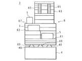
図2は、実施の形態1に係る撮像モジュール3の側面図である。図示の撮像モジュール3は、撮像素子4と、3つの受動部品5と、撮像素子4及び受動部品5が実装された実装基板6とを備える。 FIG. 2 is a side view of the
撮像素子4は、例えば、CMOS(Complementary Metal Oxide Semiconductor )、CCD(Charge Coupled Device )等であり、矩形の撮像面(図における下面)に結ばれる光学像を電気信号に変換して出力する。撮像素子4の背面(撮像面の反対側の面)には、入出力用の複数の電極40が縦横に並べて設けてあり、撮像素子4は、これらの電極40により実装基板6の第1面60に表面実装されている。 The
受動部品5は、撮像素子4の出力信号を処理し、撮像素子4の各画素の輝度を示す画像信号に変換して出力する処理回路を構成する電子部品、例えば、電源ラインとグランドとの間をバイパスするコンデンサ等であり、第1面60の反対側に後述の如く設けられた第2面61及び第3面62に実装されている。 The
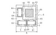
図3は、受動部品5の実装態様を示す平面図、図4は、受動部品5の実装態様を示す斜視図である。図示の如く実装基板6は、第1面60の反対側に、第2面61、第3面62及びケーブル接続ブロック63を備えている。 FIG. 3 is a plan view showing a mounting mode of the
第2面61及び第3面62は、第1面60と平行をなす受動部品5の実装面である。第2面61は、図3、図4に示す如く、実装基板6の一辺の半長に沿って、縁部から所定の幅を有して形成されている、第3面62は、前記一辺の残りの半長と該一辺に隣接する他辺に沿って、第2面61と略等しい幅を有して形成されている。第2面61と第3面62とは、図2、図4に示す如く、前記一辺の中央位置で第2面61から垂直に立ち上がる段差を介して連続している。 The
第2面61には、受動部品5を接続するための接続ランド64が一対設けられている。接続ランド64は、第2面61の幅方向に延びる矩形の導体パターンである。図3、図4に示す如く、一方の接続ランド64は、適宜のクリアランスを隔てて第2面61の端縁に沿わせてあり、他方の接続ランド64は、前記段差の立ち上がり縁にクリアランスなしに沿わせてある。受動部品5は、以上の接続ランド64、64上に架け渡すように載置され、半田リフローにより接続して実装されている。 A pair of connection lands 64 for connecting the
第3面62には、受動部品5を実装するための接続ランド64が二対設けられている。図3に示す如く、一対の接続ランド64は、段差を介して第2面61と連続する部分に設けられ、一方の接続ランド64は、前記段差の立ち下がり縁にクリアランスなしに沿わせてあり、他方の接続ランド64は、前記立ち下がり縁に対向する第3面62の端縁に適宜のクリアランスを隔てて沿わせてある。もう一対の接続ランド64は、図3に示す如く、第3面62の残りの部分に設けられ、一方の接続ランド64は、適宜のクリアランスを隔てて第3面62の端縁に沿わせてあり、他方の接続ランド64は、一方の接続ランド64から所定長離隔して配置されている。各対の接続ランド64、64上には、2つの受動部品5が夫々架け渡すように載置され、半田リフローにより接続して実装されている。図3においては、各接続ランド64にハッチングを施し、夫々の位置関係を明示している。 Two pairs of connection lands 64 for mounting the
ケーブル接続ブロック63は、第2面61及び第3面62から適宜の高さを有して立ち上がる柱状のブロックであり、図3に示す平面内で、第2面61及び第3面62を除く略全面を占める矩形断面を有している。ケーブル接続ブロック63の4つの側面には、ケーブル接続ランド65が設けられ、ケーブル接続ブロック63の端面には、接地ランド66が設けられている。 The
ケーブル接続ランド65は、ケーブル接続ブロック63の高さ方向に延びる矩形の導体パターンであり、図3に示す如く、ケーブル接続ブロック63の3つの側面には、各2つのケーブル接続ランド65が並設され、残りの1つの側面には、1つのケーブル接続ランド65が設けられている。各ケーブル接続ランド65には、図2中に2点鎖線により示す如く、前述したケーブル17の複数の芯線が夫々接続される。 The
接地ランド66は、端面の中央部に設けられた矩形の導体パターンであり、この接地ランド66には、図2中に2点鎖線により示す如く、前述したケーブル17が備えるシールドの端部が接続される。図2及び図3においては、夫々に現れるケーブル接続ランド65及び接地ランド66にハッチングを施してある。 The grounding
以上の構成を有する実装基板6は、例えば、複数枚のセラミックス基板を厚さ方向に積層して構成することができる。図2に示す実装基板6は、12枚のセラミックス基板を積層して構成されており、第1面60に表面実装された撮像素子4は、夫々のセラミックス基板に形成された導電パターン及びビアホールにより、第2面61及び第3面62に設けられた接続ランド64、並びにケーブル接続ブロック63に設けられたケーブル接続ランド65に接続されている。図5は、導電パターン及びビアホールの形成態様を例示する説明図である。なお各図中には、導電パターンがハッチングを施して示され、各層を貫通するビアホールの位置が小円により示してある。 The mounting
図5の右下図は、図2における最下層のセラミックス基板の下面、即ち、第1面60を示しており、この面には、撮像素子4が備える複数の電極40に対応する複数の導電パターン41が縦横に並べて形成されている。図5の右側の残りの3つの図は、下から順に、最下層、2層目、3層目のセラミックス基板の上面を示している。3層目のセラミックス基板の上面の一部には、一対の接続ランド64、64を備える第2面61が設けられる。 The lower right figure of FIG. 5 shows the lower surface of the ceramic substrate of the lowermost layer in FIG. 2, that is, the
図5の左側の6つの図は、下から順に、4層目、5層目、6、7層目、8層目、9、10、11層目及び12層目のセラミックス基板の上面を示している。5層目のセラミックス基板の上面の一部には、二対の接続ランド64、64を備える第3面62が設けられる。6層目以降のセラミックス基板は、ケーブル接続ブロック63を構成しており、ケーブル接続ランド65は、8〜11層目のセラミックス基板の側面に連続する導電パターンとして形成され、8層目のセラミックス基板に設けられた導電パターンにより内側のビアホールに接続される。12層目(最上層)のセラミックス基板の上面には、接地ランド66が設けられる。 The six figures on the left side of FIG. 5 show the upper surfaces of the fourth, fifth, sixth, seventh, eighth, ninth, tenth, eleventh, and twelfth ceramic substrates in this order from the bottom. ing. A
実施の形態1に係る撮像モジュール3において、第1面60に撮像素子4を表面実装してある実装基板6は、第1面60の反対側に、複数の受動部品5の接続ランド64が設けられた第2面61及び第3面62を備え、第2面61と第3面62とは、段差を介して連続している。接続ランド64の配置は、夫々の受動部品5の接続に際し、半田ブリッジによる短絡を防止するため、相隣する接続ランド64間に所定のクリアランスを保てるように設定する必要がある。 In the
ここで、第2面61と第3面62との間には段差が存在しており、この段差は、第2面61及び第3面62に設けられる接続ランド64との間の3次元的なクリアランスとしての機能を果たす。従って、第2面61に設けられる接続ランド64と、この接続ランド64と隣り合って第3面62に設けられる接続ランド64との間には、平面的なクリアランスを確保する必要がなく、前述したように、クリアランスなしに段差に沿わせた接続ランド64の配置が可能である。 Here, there is a step between the
このような配置により、図3に示す如く、第2面61に実装される受動部品5と、第3面62に実装される受動部品5とを、平面視において近接して長さ方向に並べることができ、図3中のA寸法を前記クリアランスの相当分だけ小さくすることができる。第3面62上の2つの受動部品5は、長さ方向を直交させた配置であり、相隣する接続ランド64間のクリアランスの確保は容易である。実装基板6の縦横寸法を小さくし、軸直角断面において撮像素子4以下の投影面積を有する実装基板6を実現することができる。 With such an arrangement, as shown in FIG. 3, the
以上の如く構成された撮像モジュール3は、前述の如く内視鏡1に組み込まれた場合、挿入管10の先端部において、対物レンズ15に対向する撮像素子4の撮像面に相当する最小限の占有面積しか必要とせず、挿入管10の細径化要求に応えることができる。実装基板6の軸方向寸法は、第2面61と第3面62との間の段差の高さ相当分だけ増大するが、この増大量はわずかであり、先端部の向きを変える動作を阻害しない。 When the
また撮像モジュール3は、柱状のケーブル接続ブロック63を備え、該ケーブル接続ブロック63の側面には、複数のケーブル接続ランド65が設けてある。撮像モジュール3へのケーブル17の接続は、図2に示す如く、ケーブル接続ブロック63と略同軸上に対向させたケーブル17の端部から制御線、信号線等の複数の芯線を引き出し、各芯線を対応するケーブル接続ランド65の夫々に接続する手順により、容易、且つ確実に実現することができる。 Further, the
ケーブル接続ブロック63の端面には、接地ランド66が設けてある。ケーブル17が備えるシールドは、接地ランド66への接続により容易に接地することができ、電磁ノイズ、静電ノイズの影響を排除することができる。 A grounding
(実施の形態2)
図6は、実施の形態2に係る撮像モジュール3の側面図、図7は、受動部品5の実装態様を示す平面図である。実施の形態2の撮像モジュール3において、実装基板6は、撮像素子4が表面実装された第1面60の反対側に、実施の形態1と同様、第2面61、第3面62及びケーブル接続ブロック63を備え、更に、第4面67を備えている。(Embodiment 2)
FIG. 6 is a side view of the
第2面61、第3面62及び第4面67は、第1面60と平行をなす受動部品5の実装面である。第2面61は、実施の形態1と同様、実装基板6の一辺の半長に沿って形成されている、第3面62は、前記一辺の残りの半長に沿って形成され、第2面61と第3面62とは、第2面61から垂直に立ち上がる段差を介して連続している。第4面67は、前記一辺に隣接する他辺に沿って形成され、第3面62と第4面67とは、第3面62から垂直に立ち上がる段差を介して連続している。 The
第2面61、第3面62及び第4面67には、受動部品5を接続するための接続ランド64が各一対設けられ、受動部品5は、各対の接続ランド64、64上に架け渡すように載置され、半田リフローにより接続して実装されている。第2面61及び第3面62において、段差の側に位置する接続ランド64は、実施の形態1と同様、段差との間にクリアランスなしに沿わせてある。第4面67においても、段差の側に位置する接続ランド64は、段差の立ち下がり縁にクリアランスなしに沿わせてある。 A pair of connection lands 64 for connecting the
実施の形態2に係る撮像モジュール3においては、第4面67に設けられる一方の接続ランド64を段差の立ち下がり縁にクリアランスなしに沿わせて配置することができ、実施の形態1と同様に、図7中のA寸法を小さくすることができる上、図7中のB寸法をクリアランスの相当分だけ小さくすることができる。従って、実装基板6の縦横寸法を更に小さくし、軸直角断面において撮像素子4以下の投影面積を有する実装基板6を実現することができる。 In the
以上の実施の形態2においては、第3面62と第4面67とが、第3面62から立ち上がる段差を介して連続する構成としたが、第3面62から立ち下がる段差を介して連続する構成としてもよい。 In the second embodiment described above, the
図6、図7に示す実施の形態2に係る撮像モジュール3の他の構成は、図2、図3に示す実施の形態1に係る撮像モジュール3と同様であり、対応する構成要素に実施の形態1と同一の参照符号を付して説明を省略する。 Other configurations of the
なお、今回開示された実施の形態は、すべての点で例示であって制限的なものではないと考えられるべきである。本発明の範囲は、上記した意味ではなく、特許請求の範囲によって示され、特許請求の範囲と均等な意味および範囲内でのすべての変更が含まれることが意図される。 It should be noted that the embodiments disclosed this time are exemplary in all respects and are not considered to be restrictive. The scope of the present invention is indicated by the scope of claims, not the above-mentioned meaning, and is intended to include all modifications within the meaning and scope equivalent to the scope of claims.
1 内視鏡
3 撮像モジュール
4 撮像素子
5 受動部品
6 実装基板
10 挿入管
17 ケーブル
60 第1面
61 第2面
62 第3面
63 ケーブル接続ブロック
64 接続ランド
65 ケーブル接続ランド
66 接地ランド
67 第4面1
Claims (6)
Translated fromJapanese前記実装基板は、
前記撮像素子が表面実装された第1面と、
該第1面の反対側に位置し、前記受動部品の接続ランドが設けられた第2面と、
該第2面と段差を介して連続し、前記受動部品の接続ランドが設けられた第3面と、
前記第2面及び第3面から立ち上がり、ケーブルが接続される柱状のケーブル接続ブロックと
を備える撮像モジュール。In an image pickup module including an image pickup element and a mounting substrate on which the image pickup element is mounted together with a plurality of passive components.
The mounting board is
The first surface on which the image sensor is surface-mounted and
A second surface located on the opposite side of the first surface and provided with a connection land for the passive component,
A third surface that is continuous with the second surface via a step and is provided with a connection land for the passive component.
An imaging module including a columnar cable connection block that rises from the second and third surfaces and to which cables are connected.
前記撮像モジュールは、
撮像素子と、該撮像素子を複数の受動部品と共に実装する実装基板とを備え、
前記実装基板は、
前記撮像素子が表面面実装された第1面と、
該第1面の反対側に位置し、前記受動部品の接続ランドが設けられた第2面と、
該第2面と段差を介して連続し、前記受動部品の接続ランドが設けられた第3面と、
前記第2面及び第3面から立ち上がり、ケーブルが接続される柱状のケーブル接続ブロックと
を備える内視鏡。In an endoscope having an imaging module built into the tip of an intubation
The imaging module
It includes an image pickup device and a mounting board on which the image pickup device is mounted together with a plurality of passive components.
The mounting board is
The first surface on which the image sensor is mounted on the surface surface and
A second surface located on the opposite side of the first surface and provided with a connection land for the passive component,
A third surface that is continuous with the second surface via a step and is provided with a connection land for the passive component.
An endoscope having a columnar cable connection block that rises from the second and third surfaces and to which cables are connected.
Priority Applications (5)
| Application Number | Priority Date | Filing Date | Title |
|---|---|---|---|
| JP2019061430AJP6792661B2 (en) | 2019-03-27 | 2019-03-27 | Imaging module and endoscope |
| DE112020000068.0TDE112020000068T5 (en) | 2019-03-27 | 2020-03-12 | IMAGING MODULE AND ENDOSCOPE |
| US17/259,735US11903566B2 (en) | 2019-03-27 | 2020-03-12 | Imaging module and endoscope having image sensor and mounting board |
| PCT/JP2020/010707WO2020195872A1 (en) | 2019-03-27 | 2020-03-12 | Imaging module and endoscope |
| CN202080004092.4ACN112470057B (en) | 2019-03-27 | 2020-03-12 | Image pickup module and endoscope |
Applications Claiming Priority (1)
| Application Number | Priority Date | Filing Date | Title |
|---|---|---|---|
| JP2019061430AJP6792661B2 (en) | 2019-03-27 | 2019-03-27 | Imaging module and endoscope |
Publications (2)
| Publication Number | Publication Date |
|---|---|
| JP2020156901Atrue JP2020156901A (en) | 2020-10-01 |
| JP6792661B2 JP6792661B2 (en) | 2020-11-25 |
Family
ID=72608708
Family Applications (1)
| Application Number | Title | Priority Date | Filing Date |
|---|---|---|---|
| JP2019061430AActiveJP6792661B2 (en) | 2019-03-27 | 2019-03-27 | Imaging module and endoscope |
Country Status (5)
| Country | Link |
|---|---|
| US (1) | US11903566B2 (en) |
| JP (1) | JP6792661B2 (en) |
| CN (1) | CN112470057B (en) |
| DE (1) | DE112020000068T5 (en) |
| WO (1) | WO2020195872A1 (en) |
Families Citing this family (1)
| Publication number | Priority date | Publication date | Assignee | Title |
|---|---|---|---|---|
| CN115278040B (en)* | 2022-09-28 | 2023-01-03 | 常州联影智融医疗科技有限公司 | Electronic circuit unit and imaging unit |
Citations (6)
| Publication number | Priority date | Publication date | Assignee | Title |
|---|---|---|---|---|
| JPH08146310A (en)* | 1994-11-18 | 1996-06-07 | Olympus Optical Co Ltd | Solid-state image pickup device |
| JP2006025852A (en)* | 2004-07-12 | 2006-02-02 | Texas Instr Japan Ltd | Imaging module for endoscope |
| JP2008177298A (en)* | 2007-01-17 | 2008-07-31 | Olympus Corp | Laminated mounting structure |
| US20160205296A1 (en)* | 2013-09-30 | 2016-07-14 | Olympus Corporation | Imaging unit and endoscope apparatus |
| US20170255001A1 (en)* | 2014-12-08 | 2017-09-07 | Olympus Corporation | Imaging unit, endoscope, and method of manufacturing imaging unit |
| WO2018078766A1 (en)* | 2016-10-27 | 2018-05-03 | オリンパス株式会社 | Imaging unit, endoscope, and imaging unit production method |
Family Cites Families (22)
| Publication number | Priority date | Publication date | Assignee | Title |
|---|---|---|---|---|
| US7914442B1 (en)* | 1999-03-01 | 2011-03-29 | Gazdzinski Robert F | Endoscopic smart probe and method |
| EP1982636B2 (en)* | 2001-06-18 | 2016-09-07 | Given Imaging Ltd. | In vivo sensing device with a circuit board having rigid sections and flexible sections |
| JP2007244747A (en)* | 2006-03-17 | 2007-09-27 | Olympus Medical Systems Corp | Imaging device and method for assembling the imaging device |
| JP5173926B2 (en)* | 2009-05-12 | 2013-04-03 | オリンパスメディカルシステムズ株式会社 | IMAGING DEVICE AND IMAGING DEVICE MANUFACTURING METHOD |
| WO2011030608A1 (en)* | 2009-09-11 | 2011-03-17 | オリンパスメディカルシステムズ株式会社 | Image pickup device and method for manufacturing image pickup device |
| JP5913870B2 (en)* | 2011-08-31 | 2016-04-27 | オリンパス株式会社 | Capsule medical device |
| JP5757852B2 (en)* | 2011-12-05 | 2015-08-05 | オリンパス株式会社 | Imaging module and imaging unit |
| CN104684455B (en)* | 2013-06-28 | 2017-05-10 | 奥林巴斯株式会社 | Imaging module and endoscope device |
| JP6344935B2 (en) | 2014-03-13 | 2018-06-20 | Hoya株式会社 | Semiconductor device and endoscope |
| JP5871217B2 (en)* | 2014-06-11 | 2016-03-01 | パナソニックIpマネジメント株式会社 | Endoscope |
| JP6261473B2 (en) | 2014-08-08 | 2018-01-17 | Hoya株式会社 | Electronic scope and method of manufacturing electronic scope |
| EP3231350A4 (en)* | 2014-12-08 | 2018-08-01 | Olympus Corporation | Imaging unit, imaging module, and endoscope system |
| WO2016189679A1 (en)* | 2015-05-27 | 2016-12-01 | オリンパス株式会社 | Image pickup apparatus and endoscope |
| CN107710730B (en)* | 2016-01-28 | 2020-05-05 | 奥林巴斯株式会社 | Image pickup unit, image pickup module, and endoscope |
| CN109195501B (en)* | 2016-05-19 | 2021-06-04 | 奥林巴斯株式会社 | Cable connection circuit board, imaging device, endoscope, and method for manufacturing imaging device |
| DE112017006139T5 (en)* | 2016-12-05 | 2019-08-22 | Olympus Corporation | ELECTRONIC SWITCHING UNIT, IMAGING UNIT, ENDOSCOPE AND METHOD OF CONNECTING AN ELECTRONIC SWITCHING UNIT |
| WO2019138606A1 (en)* | 2018-01-11 | 2019-07-18 | オリンパス株式会社 | Oblique endoscope |
| WO2019163175A1 (en)* | 2018-02-20 | 2019-08-29 | オリンパス株式会社 | Image pickup unit and endoscope |
| WO2019207650A1 (en)* | 2018-04-24 | 2019-10-31 | オリンパス株式会社 | Endoscope imaging device, endoscope, and manufacturing method for endoscope imaging device |
| JP6643396B2 (en)* | 2018-05-09 | 2020-02-12 | 株式会社フジクラ | Three-dimensional wiring board, imaging unit |
| TWI761974B (en)* | 2020-09-29 | 2022-04-21 | 醫電鼎眾股份有限公司 | Modular combination of endoscope light source and imaging module |
| WO2022244133A1 (en)* | 2021-05-19 | 2022-11-24 | オリンパスメディカルシステムズ株式会社 | Imaging unit, method for producing imaging unit, and endoscope |
- 2019
- 2019-03-27JPJP2019061430Apatent/JP6792661B2/enactiveActive
- 2020
- 2020-03-12CNCN202080004092.4Apatent/CN112470057B/enactiveActive
- 2020-03-12DEDE112020000068.0Tpatent/DE112020000068T5/enactivePending
- 2020-03-12WOPCT/JP2020/010707patent/WO2020195872A1/ennot_activeCeased
- 2020-03-12USUS17/259,735patent/US11903566B2/enactiveActive
Patent Citations (6)
| Publication number | Priority date | Publication date | Assignee | Title |
|---|---|---|---|---|
| JPH08146310A (en)* | 1994-11-18 | 1996-06-07 | Olympus Optical Co Ltd | Solid-state image pickup device |
| JP2006025852A (en)* | 2004-07-12 | 2006-02-02 | Texas Instr Japan Ltd | Imaging module for endoscope |
| JP2008177298A (en)* | 2007-01-17 | 2008-07-31 | Olympus Corp | Laminated mounting structure |
| US20160205296A1 (en)* | 2013-09-30 | 2016-07-14 | Olympus Corporation | Imaging unit and endoscope apparatus |
| US20170255001A1 (en)* | 2014-12-08 | 2017-09-07 | Olympus Corporation | Imaging unit, endoscope, and method of manufacturing imaging unit |
| WO2018078766A1 (en)* | 2016-10-27 | 2018-05-03 | オリンパス株式会社 | Imaging unit, endoscope, and imaging unit production method |
Also Published As
| Publication number | Publication date |
|---|---|
| US11903566B2 (en) | 2024-02-20 |
| US20220000352A1 (en) | 2022-01-06 |
| JP6792661B2 (en) | 2020-11-25 |
| DE112020000068T5 (en) | 2021-04-01 |
| WO2020195872A1 (en) | 2020-10-01 |
| CN112470057A (en) | 2021-03-09 |
| CN112470057B (en) | 2022-12-23 |
Similar Documents
| Publication | Publication Date | Title |
|---|---|---|
| WO2014171482A1 (en) | Image capturing device and electronic endoscope | |
| US9345395B2 (en) | Imaging module and endoscope device | |
| US12011145B2 (en) | Endoscope distal end structure and endoscope | |
| US20180049627A1 (en) | Imaging unit and endoscope | |
| JP7272632B2 (en) | Endoscope | |
| JP6344935B2 (en) | Semiconductor device and endoscope | |
| JP6792661B2 (en) | Imaging module and endoscope | |
| JP6243565B2 (en) | Endoscope system | |
| US12082784B2 (en) | Electronic module, method of manufacturing electronic module, and endoscope | |
| JP6099541B2 (en) | Endoscope and endoscope manufacturing method | |
| TWI814107B (en) | Image capturing assembly and related endoscope | |
| JP6321917B2 (en) | Imaging apparatus and electronic endoscope | |
| JP6321916B2 (en) | Imaging apparatus and electronic endoscope | |
| JP6736377B2 (en) | Electronic endoscopic device | |
| JP6646342B2 (en) | Substrate assembly and electronic endoscope system | |
| WO2024203054A1 (en) | Mounting substrate and endoscope | |
| JP2001311879A (en) | Endoscope and its manufacturing method | |
| US20240090756A1 (en) | Endoscopic System with Electrical Bridge in Distal Tip | |
| JP2019129503A (en) | Imaging module | |
| JP7029296B2 (en) | Endoscope board unit | |
| JP2017086326A (en) | Circuit board unit, imaging device, and endoscope | |
| JP2016052434A (en) | Electronic scope for endoscope and assembling method of electronic scope for endoscope | |
| JP2024055540A (en) | The camera module | |
| JP2021037161A (en) | Light module and endoscope | |
| JP2015080633A (en) | Electrical unit and endoscope apparatus using the electrical unit |
Legal Events
| Date | Code | Title | Description |
|---|---|---|---|
| A621 | Written request for application examination | Free format text:JAPANESE INTERMEDIATE CODE: A621 Effective date:20201007 | |
| A871 | Explanation of circumstances concerning accelerated examination | Free format text:JAPANESE INTERMEDIATE CODE: A871 Effective date:20201007 | |
| A975 | Report on accelerated examination | Free format text:JAPANESE INTERMEDIATE CODE: A971005 Effective date:20201016 | |
| TRDD | Decision of grant or rejection written | ||
| A01 | Written decision to grant a patent or to grant a registration (utility model) | Free format text:JAPANESE INTERMEDIATE CODE: A01 Effective date:20201020 | |
| A61 | First payment of annual fees (during grant procedure) | Free format text:JAPANESE INTERMEDIATE CODE: A61 Effective date:20201106 | |
| R150 | Certificate of patent or registration of utility model | Ref document number:6792661 Country of ref document:JP Free format text:JAPANESE INTERMEDIATE CODE: R150 | |
| R250 | Receipt of annual fees | Free format text:JAPANESE INTERMEDIATE CODE: R250 | |
| R250 | Receipt of annual fees | Free format text:JAPANESE INTERMEDIATE CODE: R250 |