JP2020136545A - Solid-state imaging device and electronic apparatus - Google Patents
Solid-state imaging device and electronic apparatusDownload PDFInfo
- Publication number
- JP2020136545A JP2020136545AJP2019029911AJP2019029911AJP2020136545AJP 2020136545 AJP2020136545 AJP 2020136545AJP 2019029911 AJP2019029911 AJP 2019029911AJP 2019029911 AJP2019029911 AJP 2019029911AJP 2020136545 AJP2020136545 AJP 2020136545A
- Authority
- JP
- Japan
- Prior art keywords
- image sensor
- solid
- semiconductor substrate
- glass substrate
- state image
- Prior art date
- Legal status (The legal status is an assumption and is not a legal conclusion. Google has not performed a legal analysis and makes no representation as to the accuracy of the status listed.)
- Pending
Links
Images


Classifications
- G—PHYSICS
- G02—OPTICS
- G02B—OPTICAL ELEMENTS, SYSTEMS OR APPARATUS
- G02B3/00—Simple or compound lenses
- G02B3/0006—Arrays
- G02B3/0037—Arrays characterized by the distribution or form of lenses
- G02B3/0056—Arrays characterized by the distribution or form of lenses arranged along two different directions in a plane, e.g. honeycomb arrangement of lenses
- H—ELECTRICITY
- H01—ELECTRIC ELEMENTS
- H01L—SEMICONDUCTOR DEVICES NOT COVERED BY CLASS H10
- H01L23/00—Details of semiconductor or other solid state devices
- H01L23/544—Marks applied to semiconductor devices or parts, e.g. registration marks, alignment structures, wafer maps
- H—ELECTRICITY
- H04—ELECTRIC COMMUNICATION TECHNIQUE
- H04N—PICTORIAL COMMUNICATION, e.g. TELEVISION
- H04N25/00—Circuitry of solid-state image sensors [SSIS]; Control thereof
- H04N25/70—SSIS architectures; Circuits associated therewith
- H—ELECTRICITY
- H10—SEMICONDUCTOR DEVICES; ELECTRIC SOLID-STATE DEVICES NOT OTHERWISE PROVIDED FOR
- H10F—INORGANIC SEMICONDUCTOR DEVICES SENSITIVE TO INFRARED RADIATION, LIGHT, ELECTROMAGNETIC RADIATION OF SHORTER WAVELENGTH OR CORPUSCULAR RADIATION
- H10F39/00—Integrated devices, or assemblies of multiple devices, comprising at least one element covered by group H10F30/00, e.g. radiation detectors comprising photodiode arrays
- H10F39/011—Manufacture or treatment of image sensors covered by group H10F39/12
- H—ELECTRICITY
- H10—SEMICONDUCTOR DEVICES; ELECTRIC SOLID-STATE DEVICES NOT OTHERWISE PROVIDED FOR
- H10F—INORGANIC SEMICONDUCTOR DEVICES SENSITIVE TO INFRARED RADIATION, LIGHT, ELECTROMAGNETIC RADIATION OF SHORTER WAVELENGTH OR CORPUSCULAR RADIATION
- H10F39/00—Integrated devices, or assemblies of multiple devices, comprising at least one element covered by group H10F30/00, e.g. radiation detectors comprising photodiode arrays
- H10F39/80—Constructional details of image sensors
- H10F39/804—Containers or encapsulations
- H—ELECTRICITY
- H10—SEMICONDUCTOR DEVICES; ELECTRIC SOLID-STATE DEVICES NOT OTHERWISE PROVIDED FOR
- H10F—INORGANIC SEMICONDUCTOR DEVICES SENSITIVE TO INFRARED RADIATION, LIGHT, ELECTROMAGNETIC RADIATION OF SHORTER WAVELENGTH OR CORPUSCULAR RADIATION
- H10F39/00—Integrated devices, or assemblies of multiple devices, comprising at least one element covered by group H10F30/00, e.g. radiation detectors comprising photodiode arrays
- H10F39/80—Constructional details of image sensors
- H10F39/805—Coatings
- H10F39/8057—Optical shielding
- H—ELECTRICITY
- H10—SEMICONDUCTOR DEVICES; ELECTRIC SOLID-STATE DEVICES NOT OTHERWISE PROVIDED FOR
- H10F—INORGANIC SEMICONDUCTOR DEVICES SENSITIVE TO INFRARED RADIATION, LIGHT, ELECTROMAGNETIC RADIATION OF SHORTER WAVELENGTH OR CORPUSCULAR RADIATION
- H10F39/00—Integrated devices, or assemblies of multiple devices, comprising at least one element covered by group H10F30/00, e.g. radiation detectors comprising photodiode arrays
- H10F39/80—Constructional details of image sensors
- H10F39/806—Optical elements or arrangements associated with the image sensors
- H10F39/8063—Microlenses
- H—ELECTRICITY
- H01—ELECTRIC ELEMENTS
- H01L—SEMICONDUCTOR DEVICES NOT COVERED BY CLASS H10
- H01L2223/00—Details relating to semiconductor or other solid state devices covered by the group H01L23/00
- H01L2223/544—Marks applied to semiconductor devices or parts
- H01L2223/54426—Marks applied to semiconductor devices or parts for alignment
- H—ELECTRICITY
- H01—ELECTRIC ELEMENTS
- H01L—SEMICONDUCTOR DEVICES NOT COVERED BY CLASS H10
- H01L2223/00—Details relating to semiconductor or other solid state devices covered by the group H01L23/00
- H01L2223/544—Marks applied to semiconductor devices or parts
- H01L2223/54473—Marks applied to semiconductor devices or parts for use after dicing
- H01L2223/54486—Located on package parts, e.g. encapsulation, leads, package substrate
Landscapes
- Physics & Mathematics (AREA)
- Engineering & Computer Science (AREA)
- General Physics & Mathematics (AREA)
- Condensed Matter Physics & Semiconductors (AREA)
- Computer Hardware Design (AREA)
- Microelectronics & Electronic Packaging (AREA)
- Power Engineering (AREA)
- Signal Processing (AREA)
- Optics & Photonics (AREA)
- Multimedia (AREA)
- Solid State Image Pick-Up Elements (AREA)
- Transforming Light Signals Into Electric Signals (AREA)
- Internal Circuitry In Semiconductor Integrated Circuit Devices (AREA)
Abstract
Description
Translated fromJapanese本開示は、固体撮像装置及び電子機器に関する。 The present disclosure relates to a solid-state image sensor and an electronic device.
近年、カメラ付き移動体端末装置やデジタルスチルカメラなどの電子機器において、カメラの高画素化、小型化及び薄型化が進んでいる。小型化や薄型化の手法としては、固体撮像素子をCSP(Chip Size Package)型にすることが一般的である。 In recent years, in electronic devices such as mobile terminal devices with cameras and digital still cameras, the number of pixels of cameras has been increased, the size has been reduced, and the thickness has been reduced. As a method of miniaturization or thinning, it is common to make the solid-state image sensor a CSP (Chip Size Package) type.
しかしながら、固体撮像装置をCSP型とした場合、撮像装置内での光の反射や回折によってフレア現象が発生し、それにより、画質が低下してしまう場合が存在した。 However, when the solid-state image sensor is a CSP type, a flare phenomenon occurs due to reflection or diffraction of light in the image sensor, and as a result, the image quality may deteriorate.
そこで本開示では、画質の低下を抑制することが可能な固体撮像装置及び電子機器を提案する。 Therefore, the present disclosure proposes a solid-state image sensor and an electronic device capable of suppressing deterioration of image quality.
上記の課題を解決するために、本開示に係る一形態の固体撮像装置は、受光素子を備える半導体基板と、前記半導体基板の第1面に配置されたオンチップレンズと、前記オンチップレンズを覆う樹脂層と、前記半導体基板の前記第1面側に前記樹脂層と離間して配置されたガラス基板とを備える。 In order to solve the above problems, the solid-state imaging device according to the present disclosure includes a semiconductor substrate including a light receiving element, an on-chip lens arranged on the first surface of the semiconductor substrate, and the on-chip lens. A resin layer to cover the semiconductor substrate and a glass substrate arranged on the first surface side of the semiconductor substrate so as to be separated from the resin layer are provided.
以下に、本開示の一実施形態について図面に基づいて詳細に説明する。なお、以下の実施形態において、同一の部位には同一の符号を付することにより重複する説明を省略する。 Hereinafter, one embodiment of the present disclosure will be described in detail with reference to the drawings. In the following embodiments, the same parts are designated by the same reference numerals, so that duplicate description will be omitted.
また、以下に示す項目順序に従って本開示を説明する。
1.第1の実施形態
1.1 電子機器の構成例
1.2 固体撮像装置の構成例
1.3 単位画素の構成例
1.4 単位画素の基本機能例
1.5 固体撮像装置の積層構造例
1.6 フレア現象
1.7 断面構造例
1.8 製造方法
1.9 作用・効果
1.10 変形例
2.第2の実施形態
2.1 断面構造例
2.2 製造方法
2.2.1 製造方法の変形例
2.3 樹脂層のレンズ機能
2.4 瞳補正
2.5 作用・効果
2.6 ガラス基板の変形例
2.6.1 第1変形例
2.6.2 第2変形例
2.6.3 第3変形例
2.6.4 第4変形例
3.第3の実施形態
3.1 断面構造例
3.2 製造方法
3.3 作用・効果
4.第4の実施形態
4.1 断面構造例
4.2 製造方法
4.2.1 製造方法の変形例
4.3 作用・効果
5.第5の実施形態
5.1 断面構造例
5.2 製造方法
5.3 作用・効果
6.第6の実施形態
6.1 断面構造例
6.2 製造方法
6.3 作用・効果In addition, the present disclosure will be described according to the order of items shown below.
1. 1. 1st Embodiment 1.1 Configuration example of electronic device 1.2 Configuration example of solid-state image sensor 1.3 Configuration example of unit pixel 1.4 Basic function example of unit pixel 1.5 Stacked structure example of solid-state image sensor 1 .6 Flare phenomenon 1.7 Cross-sectional structure example 1.8 Manufacturing method 1.9 Action / effect 1.10 Deformation example 2. 2nd Embodiment 2.1 Cross-sectional structure example 2.2 Manufacturing method 2.2.1 Modification example of manufacturing method 2.3 Lens function of resin layer 2.4 Eye correction 2.5 Action / effect 2.6 Glass substrate 2.6.1 1st modification 2.6.2 2nd modification 2.6.3 3rd modification 2.6.4 4th modification 3. Third Embodiment 3.1 Cross-sectional structure example 3.2 Manufacturing method 3.3 Action / effect 4. Fourth Embodiment 4.1 Cross-sectional structure example 4.2 Manufacturing method 4.2.1 Modification example of manufacturing method 4.3 Action / effect 5. Fifth Embodiment 5.1 Cross-sectional structure example 5.2 Manufacturing method 5.3 Action / effect 6. Sixth Embodiment 6.1 Cross-sectional structure example 6.2 Manufacturing method 6.3 Action / effect
1.第1の実施形態
まず、第1の実施形態に係る固体撮像装置及び電子機器について、図面を参照して詳細に説明する。1. 1. First Embodiment First, the solid-state image sensor and the electronic device according to the first embodiment will be described in detail with reference to the drawings.
1.1 電子機器の構成例
図1は、第1の実施形態に係る固体撮像装置を搭載した電子機器の概略構成例を示すブロック図である。図1に示すように、電子機器1000は、例えば、撮像レンズ1020と、固体撮像装置100と、記憶部1030と、プロセッサ1040とを備える。1.1 Configuration Example of Electronic Device FIG. 1 is a block diagram showing a schematic configuration example of an electronic device equipped with the solid-state image sensor according to the first embodiment. As shown in FIG. 1, the
撮像レンズ1020は、入射光を集光してその像を固体撮像装置100の受光面に結像する光学系の一例である。受光面とは、固体撮像装置100における光電変換素子が配列する面であってよい。固体撮像装置100は、入射光を光電変換して画像データを生成する。また、固体撮像装置100は、生成した画像データに対し、ノイズ除去やホワイトバランス調整等の所定の信号処理を実行する。 The
記憶部1030は、例えば、フラッシュメモリやDRAM(Dynamic Random Access Memory)やSRAM(Static Random Access Memory)等で構成され、固体撮像装置100から入力された画像データ等を記録する。 The
プロセッサ1040は、例えば、CPU(Central Processing Unit)等を用いて構成され、オペレーティングシステムや各種アプリケーションソフトウエア等を実行するアプリケーションプロセッサや、GPU(Graphics Processing Unit)やベースバンドプロセッサなどが含まれ得る。プロセッサ1040は、固体撮像装置100から入力された画像データや記憶部1030から読み出した画像データ等に対し、必要に応じた種々処理を実行したり、ユーザへの表示を実行したり、所定のネットワークを介して外部へ送信したりする。 The
1.2 固体撮像装置の構成例
図2は、第1の実施形態に係るCMOS(Complementary Metal-Oxide-Semiconductor)型の固体撮像装置(以下、単にイメージセンサという)の概略構成例を示すブロック図である。ここで、CMOS型のイメージセンサとは、CMOSプロセスを応用して、または、部分的に使用して作成されたイメージセンサである。第1の実施形態に係るイメージセンサ100は、入射面が半導体基板における素子形成面とは反対側の面(以下、裏面という)側である、いわゆる裏面照射型であってもよいし、表面側である、いわゆる表面照射型であってもよい。1.2 Configuration Example of Solid-State Image Sensor FIG. 2 is a block diagram showing a schematic configuration example of a CMOS (Complementary Metal-Oxide-Semiconductor) type solid-state image sensor (hereinafter, simply referred to as an image sensor) according to the first embodiment. Is. Here, the CMOS type image sensor is an image sensor created by applying or partially using a CMOS process. The
図2に示すように、イメージセンサ100は、例えば、画素アレイ部101と、垂直駆動回路102と、カラム処理回路103と、水平駆動回路104と、システム制御部105と、信号処理部108と、データ格納部109とを備える。以下の説明において、垂直駆動回路102、カラム処理回路103、水平駆動回路104、システム制御部105、信号処理部108及びデータ格納部109は、周辺回路とも称される。 As shown in FIG. 2, the
画素アレイ部101は、受光した光量に応じた電荷を生成しかつ蓄積する光電変換素子を有する単位画素(以下、単に「画素」と記述する場合もある)110が行方向及び列方向に、すなわち、行列状に2次元格子状(以下、行列状という)に配置された構成を有する。ここで、行方向とは画素行の画素の配列方向(図面中、横方向)をいい、列方向とは画素列の画素の配列方向(図面中、縦方向)をいう。単位画素の具体的な回路構成や画素構造の詳細については後述する。 In the
画素アレイ部101では、行列状の画素配列に対し、画素行ごとに画素駆動線LDが行方向に沿って配線され、画素列ごとに垂直信号線VSLが列方向に沿って配線されている。画素駆動線LDは、画素から信号を読み出す際の駆動を行うための駆動信号を伝送する。図2では、画素駆動線LDが1本ずつの配線として示されているが、1本ずつに限られるものではない。画素駆動線LDの一端は、垂直駆動回路102の各行に対応した出力端に接続されている。 In the
垂直駆動回路102は、シフトレジスタやアドレスデコーダなどによって構成され、画素アレイ部101の各画素を全画素同時あるいは行単位等で駆動する。すなわち、垂直駆動回路102は、当該垂直駆動回路102を制御するシステム制御部105と共に、画素アレイ部101の各画素の動作を制御する駆動部を構成している。この垂直駆動回路102はその具体的な構成については図示を省略するが、一般的に、読出し走査系と掃出し走査系との2つの走査系を備えている。 The
読出し走査系は、単位画素から信号を読み出すために、画素アレイ部101の単位画素を行単位で順に選択走査する。単位画素から読み出される信号はアナログ信号である。掃出し走査系は、読出し走査系によって読出し走査が行われる読出し行に対して、その読出し走査よりも露光時間分だけ先行して掃出し走査を行う。 In order to read a signal from a unit pixel, the read-out scanning system selectively scans the unit pixels of the
この掃出し走査系による掃出し走査により、読出し行の単位画素の光電変換素子から不要な電荷が掃き出されることによって当該光電変換素子がリセットされる。そして、この掃出し走査系で不要電荷を掃き出す(リセットする)ことにより、所謂電子シャッタ動作が行われる。ここで、電子シャッタ動作とは、光電変換素子の電荷を捨てて、新たに露光を開始する(電荷の蓄積を開始する)動作のことを言う。 By the sweep scanning by this sweep scanning system, the photoelectric conversion element is reset by sweeping out unnecessary charges from the photoelectric conversion element of the unit pixel of the read row. Then, the so-called electronic shutter operation is performed by sweeping (resetting) unnecessary charges with this sweep scanning system. Here, the electronic shutter operation refers to an operation of discarding the electric charge of the photoelectric conversion element and starting a new exposure (starting the accumulation of electric charge).
読出し走査系による読出し動作によって読み出される信号は、その直前の読出し動作または電子シャッタ動作以降に受光した光量に対応している。そして、直前の読出し動作による読出しタイミングまたは電子シャッタ動作による掃出しタイミングから、今回の読出し動作による読出しタイミングまでの期間が、単位画素における電荷の蓄積期間(露光期間ともいう)となる。 The signal read by the read operation by the read scanning system corresponds to the amount of light received after the read operation immediately before or the electronic shutter operation. The period from the read timing by the immediately preceding read operation or the sweep timing by the electronic shutter operation to the read timing by the current read operation is the charge accumulation period (also referred to as the exposure period) in the unit pixel.
垂直駆動回路102によって選択走査された画素行の各単位画素から出力される信号は、画素列ごとに垂直信号線VSLの各々を通してカラム処理回路103に入力される。カラム処理回路103は、画素アレイ部101の画素列ごとに、選択行の各画素から垂直信号線VSLを通して出力される信号に対して所定の信号処理を行うとともに、信号処理後の画素信号を一時的に保持する。 The signal output from each unit pixel of the pixel row selectively scanned by the
具体的には、カラム処理回路103は、信号処理として少なくとも、ノイズ除去処理、例えばCDS(Correlated Double Sampling:相関二重サンプリング)処理や、DDS(Double Data Sampling)処理を行う。例えば、CDS処理により、リセットノイズや画素内の増幅トランジスタの閾値ばらつき等の画素固有の固定パターンノイズが除去される。カラム処理回路103は、その他にも、例えば、AD(アナログ−デジタル)変換機能を備え、光電変換素子から読み出され得たアナログの画素信号をデジタル信号に変換して出力する。 Specifically, the
水平駆動回路104は、シフトレジスタやアドレスデコーダなどによって構成され、カラム処理回路103の画素列に対応する読出し回路(以下、画素回路という)を順番に選択する。この水平駆動回路104による選択走査により、カラム処理回路103において画素回路ごとに信号処理された画素信号が順番に出力される。 The
システム制御部105は、各種のタイミング信号を生成するタイミングジェネレータなどによって構成され、当該タイミングジェネレータで生成された各種のタイミングを基に、垂直駆動回路102、カラム処理回路103、及び、水平駆動回路104などの駆動制御を行う。 The
信号処理部108は、少なくとも演算処理機能を有し、カラム処理回路103から出力される画素信号に対して演算処理等の種々の信号処理を行う。データ格納部109は、信号処理部108での信号処理にあたって、その処理に必要なデータを一時的に格納する。 The
なお、信号処理部108から出力された画像データは、例えば、イメージセンサ100を搭載する電子機器1000におけるプロセッサ1040等において所定の処理が実行されたり、所定のネットワークを介して外部へ送信されたりしてもよい。 The image data output from the
1.3 単位画素の構成例
図3は、第1の実施形態に係る単位画素の概略構成例を示す回路図である。図3に示すように、単位画素110は、フォトダイオードPDと、転送トランジスタ111と、リセットトランジスタ112と、増幅トランジスタ113と、選択トランジスタ114と、浮遊拡散層FDとを備える。1.3 Configuration Example of Unit Pixel FIG. 3 is a circuit diagram showing a schematic configuration example of a unit pixel according to the first embodiment. As shown in FIG. 3, the
選択トランジスタ114のゲートには、画素駆動線LDに含まれる選択トランジスタ駆動線LD114が接続され、リセットトランジスタ112のゲートには、画素駆動線LDに含まれるリセットトランジスタ駆動線LD112が接続され、転送トランジスタ111のゲートには、画素駆動線LDに含まれる転送トランジスタ駆動線LD111が接続されている。また、増幅トランジスタ113のドレインには、カラム処理回路103に一端が接続される垂直信号線VSLが選択トランジスタ114を介して接続されている。 The selection transistor
以下の説明において、リセットトランジスタ112、増幅トランジスタ113と及び選択トランジスタ114は、まとめて画素回路とも称される。この画素回路には、浮遊拡散層FD及び/又は転送トランジスタ111が含まれてもよい。 In the following description, the
フォトダイオードPDは、入射した光を光電変換する。転送トランジスタ111は、フォトダイオードPDに発生した電荷を転送する。浮遊拡散層FDは、転送トランジスタ111が転送した電荷を蓄積する。増幅トランジスタ113は、浮遊拡散層FDに蓄積された電荷に応じた電圧値の画素信号を垂直信号線VSLに出現させる。リセットトランジスタ112は、浮遊拡散層FDに蓄積された電荷を放出する。選択トランジスタ114は、読出し対象の単位画素110を選択する。 The photodiode PD photoelectrically converts the incident light. The
フォトダイオードPDのアノードは、接地されており、カソ−ドは、転送トランジスタ111のソースに接続されている。転送トランジスタ111のドレインは、リセットトランジスタ112のソースおよび増幅トランジスタ113のゲートに接続されており、これらの接続点であるノードが浮遊拡散層FDを構成する。なお、リセットトランジスタ112のドレインは、不図示の垂直リセット入力線に接続されている。 The anode of the photodiode PD is grounded and the cascade is connected to the source of the
増幅トランジスタ113のソースは、不図示の垂直電流供給線に接続されている。増幅トランジスタ113のドレインは、選択トランジスタ114のソースに接続されており、選択トランジスタ114のドレインは、垂直信号線VSLに接続されている。 The source of the
浮遊拡散層FDは、蓄積している電荷をその電荷量に応じた電圧値の電圧に変換する。なお、浮遊拡散層FDは、例えば、対接地容量であってもよい。ただし、これに限定されず、浮遊拡散層FDは、転送トランジスタ111のドレインとリセットトランジスタ112のソースと増幅トランジスタ113のゲートとが接続するノードにキャパシタなどを意図的に接続することで付加された容量であってもよい。 The floating diffusion layer FD converts the accumulated electric charge into a voltage having a voltage value corresponding to the amount of the electric charge. The floating diffusion layer FD may have, for example, a grounding capacitance. However, the present invention is not limited to this, and the floating diffusion layer FD is added by intentionally connecting a capacitor or the like to a node to which the drain of the
1.4 単位画素の基本機能例
次に、単位画素110の基本機能について、図3を参照して説明する。リセットトランジスタ112は、垂直駆動回路102からリセットトランジスタ駆動線LD112を介して供給されるリセット信号RSTに従って、浮遊拡散層FDに蓄積されている電荷の排出(リセット)を制御する。なお、リセットトランジスタ112がオン状態であるときに転送トランジスタ111をオン状態とすることで、浮遊拡散層FDに蓄積されている電荷に加え、フォトダイオードPDに蓄積されている電荷を排出(リセット)することも可能である。1.4 Example of Basic Function of Unit Pixel Next, the basic function of the
リセットトランジスタ112のゲートにHighレベルのリセット信号RSTが入力されると、浮遊拡散層FDが垂直リセット入力線を通して印加される電圧にクランプされる。これにより、浮遊拡散層FDに蓄積されていた電荷が排出(リセット)される。 When a high level reset signal RST is input to the gate of the
また、リセットトランジスタ112のゲートにLowレベルのリセット信号RSTが入力されると、浮遊拡散層FDは、垂直リセット入力線と電気的に切断され、浮遊状態になる。 Further, when the Low level reset signal RST is input to the gate of the
フォトダイオードPDは、入射光を光電変換し、その光量に応じた電荷を生成する。生成された電荷は、フォトダイオードPDのカソード側に蓄積する。転送トランジスタ111は、垂直駆動回路102から転送トランジスタ駆動線LD111を介して供給される転送制御信号TRGに従って、フォトダイオードPDから浮遊拡散層FDへの電荷の転送を制御する。 The photodiode PD photoelectrically converts the incident light and generates an electric charge according to the amount of the light. The generated charge is accumulated on the cathode side of the photodiode PD. The
例えば、転送トランジスタ111のゲートにHighレベルの転送制御信号TRGが入力されると、フォトダイオードPDに蓄積されている電荷が浮遊拡散層FDに転送される。一方、転送トランジスタ111のゲートにLowレベルの転送制御信号TRGが供給されると、フォトダイオードPDからの電荷の転送が停止する。 For example, when a high-level transfer control signal TRG is input to the gate of the
浮遊拡散層FDは、上述したように、フォトダイオードPDから転送トランジスタ111を介して転送された電荷をその電荷量に応じた電圧値の電圧に変換する機能を持つ。したがって、リセットトランジスタ112がオフした浮遊状態では、浮遊拡散層FDの電位は、それぞれが蓄積する電荷量に応じて変調される。 As described above, the floating diffusion layer FD has a function of converting the electric charge transferred from the photodiode PD via the
増幅トランジスタ113は、そのゲートに接続された浮遊拡散層FDの電位変動を入力信号とする増幅器として機能し、その出力電圧信号は選択トランジスタ114を介して垂直信号線VSLに画素信号として出現する。 The
選択トランジスタ114は、垂直駆動回路102から選択トランジスタ駆動線LD114を介して供給される選択制御信号SELに従って、増幅トランジスタ113による画素信号の垂直信号線VSLへの出現を制御する。例えば、選択トランジスタ114のゲートにHighレベルの選択制御信号SELが入力されると、増幅トランジスタ113による画素信号が垂直信号線VSLに出現される。一方、選択トランジスタ114のゲートにLowレベルの選択制御信号SELが入力されると、垂直信号線VSLへの画素信号の出現が停止される。これにより、複数の単位画素110が接続された垂直信号線VSLにおいて、選択した単位画素110の出力のみを取り出すことが可能となる。 The
1.5 固体撮像装置の積層構造例
図4は、第1の実施形態に係るイメージセンサの積層構造例を示す図である。図4に示すように、イメージセンサ100は、受光チップ121と回路チップ122とが上下に積層されたスタック構造を備える。受光チップ121は、例えば、フォトダイオードPDが配列する画素アレイ部101を備える半導体チップであり、回路チップ122は、例えば、図3に示す画素回路や、図2における周辺回路等を備える半導体チップである。1.5 Example of Stacked Structure of Solid-State Image Sensor FIG. 4 is a diagram showing an example of a stacked structure of an image sensor according to the first embodiment. As shown in FIG. 4, the
受光チップ121と回路チップ122との接合には、例えば、それぞれの接合面を平坦化して両者を電子間力で貼り合わせる、いわゆる直接接合を用いることができる。ただし、これに限定されず、例えば、互いの接合面に形成された銅(Cu)製の電極パッド同士をボンディングする、いわゆるCu−Cu接合や、その他、バンプ接合などを用いることも可能である。 For the bonding between the
また、受光チップ121と回路チップ122とは、例えば、半導体基板を貫通するTSV(Through-Silicon Via)などの接続部を介して電気的に接続される。TSVを用いた接続には、例えば、受光チップ121に設けられたTSVと受光チップ121から回路チップ122にかけて設けられたTSVとの2つのTSVをチップ外表で接続する、いわゆるツインTSV方式や、受光チップ121から回路チップ122まで貫通するTSVで両者を接続する、いわゆるシェアードTSV方式などを採用することができる。 Further, the
ただし、受光チップ121と回路チップ122との接合にCu−Cu接合やバンプ接合を用いた場合には、Cu−Cu接合部やバンプ接合部を介して両者が電気的に接続される。 However, when Cu-Cu bonding or bump bonding is used to bond the
1.6 フレア現象
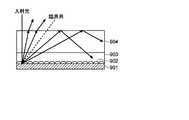
ここで、一般的なCSP型のイメージセンサで発生するフレア現象について説明する。図5は、一般的なCSP型の固体撮像装置の構造例を示す断面図である。図5に示すように、一般的なCSP型の固体撮像装置は、行列状に配列する受光素子を備える半導体チップ901の受光面と、半導体チップ901の受光面を保護するガラス基板904とが、樹脂等の接着剤903で貼り合わされた構造を備える。1.6 Flare phenomenon Here, the flare phenomenon that occurs in a general CSP type image sensor will be described. FIG. 5 is a cross-sectional view showing a structural example of a general CSP type solid-state image sensor. As shown in FIG. 5, in a general CSP type solid-state imaging device, a light receiving surface of a
半導体チップ901における受光面付近には、画素ごとのオンチップレンズ902や、画素回路におけるトランジスタなどの回路素子を接続する配線など、周期的な構造物が存在する。 In the vicinity of the light receiving surface of the
このように、半導体チップの受光面付近に周期的な構造物が存在すると、この周期的な構造物で反射した光が回折することとなるが、このように発生した回折光のうち、次数の高い成分は、ガラス基板904と大気との屈折率で決まる臨界角を越えてガラス基板904と大気との境界面に入射する。そのため、この臨界角を越える成分がガラス基板904の上面で全反射し、再度、受光面に入射することで、フレア現象が発生する。 In this way, if a periodic structure exists near the light receiving surface of the semiconductor chip, the light reflected by this periodic structure will be diffracted, but the order of the diffracted light generated in this way The high component is incident on the interface between the
特に、図5に例示するような、ガラス基板904と半導体チップ901との間が樹脂等の接着剤903で充填された、いわゆるキャビティレス構造である場合、低次の回折光であっても臨界角を越えてしまうため、回折光によるフレア光が高い光強度を持つこととなり、それにより、画質が大幅に低下してしまうという問題が発生する。 In particular, in the case of a so-called cavityless structure in which the space between the
そこで本実施形態では、回折光が全反射することで発生するフレア現象により画質の低下を抑制するために、以下のような構成を備える。 Therefore, in the present embodiment, the following configuration is provided in order to suppress deterioration of image quality due to a flare phenomenon generated by total internal reflection of diffracted light.
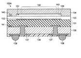
1.7 断面構造例
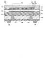
図6は、第1の実施形態に係るイメージセンサの断面構造例を示す断面図である。なお、本説明では、イメージセンサ100が裏面照射型である場合を例示するが、上述したように、表面照射型であってもよい。1.7 Cross-sectional structure example FIG. 6 is a cross-sectional view showing a cross-sectional structure example of the image sensor according to the first embodiment. In this description, the case where the
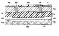
図6に示すように、イメージセンサ100は、複数の単位画素110のうちのフォトダイオードPD及び転送トランジスタ111が行列状に配列する半導体基板131と、単位画素110のうちの残りの回路素子(図3参照)及び周辺回路(図2参照)が設けられた第2半導体基板136とを含む。単位画素110におけるフォトダイオードPDは、例えば、半導体基板131における裏面側に行列状に配列していてもよい。なお、半導体基板131は、例えば、図4における受光チップ121の半導体基板であり、半導体基板136は、例えば、図4における回路チップ122の半導体基板であってよい。 As shown in FIG. 6, the
半導体基板131の裏面側(図面中、上面側)には、複数のオンチップレンズ132と、ガラス基板134と、樹脂層133とが設けられている。一方、半導体基板131の表面側(図面中、下面側)に貼り合わされた半導体基板136の裏面側(図面中、下面側)には、パッシベーション139と、引出し電極137と、ボールバンプ138とが設けられている。 A plurality of on-
オンチップレンズ132は、例えば、半導体基板131の裏面側に配列するフォトダイオードPDごとに設けられている。したがって、オンチップレンズ132は、半導体基板131の裏面に行列状に配列している。各オンチップレンズ132は、入射光をそれぞれが対応するフォトダイオードPDの受光面に集光するための曲率を備える。 The on-
ガラス基板134は、例えば、半導体基板131の裏面(受光面に相当)を保護するとともに、イメージセンサ100の物理的な強度を保つための部材である。 The
樹脂層133は、例えば、光学的に透明なエポキシ系樹脂や低融点ガラスあるいは紫外線硬化型樹脂などであり、ガラス基板134を半導体基板131に接着する役割の他に、半導体基板131の裏面における少なくとも有効画素領域150を真空又は大気等の屈折率よりも高い屈折率の材料で覆うことで、オンチップレンズ132等で反射した光の回折光が全反射する面を半導体基板131の受光面に接近させる役割を持つ。なお、有効画素領域150とは、画像データの生成に使用する単位画素110が配列する矩形の領域であってよい。 The
なお、図6では省略されているが、半導体基板131と半導体基板136とを貼り合わせる面には、それぞれ、内部に単位画素110と周辺回路とを接続する配線を含む絶縁膜より構成された配線層が設けられていてもよい。その場合、配線層の絶縁膜には、例えば、シリコン酸化膜(SiO2)やシリコン窒化膜(SiN)などを用いることができる。Although omitted in FIG. 6, the surface on which the
パッシベーション139は、例えば、感光性ポリイミドやポリベンゾオキサゾール(PBO)やシリコーン系の樹脂材料等を用いて形成された膜であり、半導体基板136の裏面(図面中、下面)側や引き出し電極137を保護する役割を持つ。 The
引出し電極137は、例えば、金属などの導電材料を用いて構成され、半導体基板136に設けられた周辺回路等に対する電気的な接続を半導体基板136の裏面まで引き出す。 The
ボールバンプ138は、例えば、引出し電極137の露出部分に設けられた半田ボール等であり、イメージセンサ100と回路基板等とを電気的に接続するための外部端子である。ただし、外部端子の構造の構造は、ボールバンプ138を用いた構造に限定されず、例えば、フラットパッドなどの構造を採用することも可能である。 The
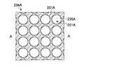
また、半導体基板131とガラス基板134とには、接合時のアライメントを取るためのアライメントマーク141及び142が設けられていてよい。 Further, the
以上のような構成において、樹脂層133は、例えば、半導体基板131の裏面における少なくとも有効画素領域150を覆う領域に設けられる。その際、上述したように、樹脂層133に、半導体基板131とガラス基板134とを接着させる役割も持たせる場合には、樹脂層133は、半導体基板131の裏面における有効画素領域150の周囲の領域にも形成される。例えば、樹脂層133は、半導体基板131の裏面全体に形成されている。 In the above configuration, the
また、ガラス基板134の半導体基板131と対向する面における少なくとも有効画素領域150と対応する領域には、溝135が設けられている。この溝135により、半導体基板131の基板厚方向において少なくとも有効画素領域150と対応する領域であって、樹脂層133とガラス基板134との間の領域に、空間(以下、エアギャップという)151が形成される。なお、基板厚方向とは、半導体基板131の表面及び裏面と垂直な方向であってよい。 Further, a
エアギャップ151の厚さ、すなわち、溝135の深さは、1μm(マイクロメートル)であって、ガラス基板134の最大の厚さの半分の深さ以下であってよい。例えば、溝135の深さは、1μm、5μm、10μm、100μm、又は、ガラス基板134の厚さとすることができる。また、エアギャップ151の内部は、真空であってもよいし、大気や窒素やアルゴン(Ar)などの気体で満たされていてもよい。 The thickness of the
このように、本実施形態では、少なくとも有効画素領域150における基板厚方向の断面構造を、半導体基板131側から順に、樹脂層133、エアギャップ151、ガラス基板134としている。言い換えれば、樹脂層133とガラス基板134との間に、樹脂層133よりも屈折率が低いエアギャップ151が介在している。 As described above, in the present embodiment, the cross-sectional structure in the substrate thickness direction at least in the
このような層構造とすることで、半導体基板131の受光面付近における周期的な構造物(オンチップレンズ132や配線等)で反射して回折した回折光が全反射する面を、樹脂層133とエアギャップ151との境界面とすることが可能となるため、言い換えれば、回折光が全反射する面を半導体基板131の受光面に近接させることが可能となるため、回折光の受光面と平行な方向への飛行距離を短くすることが可能となる。それにより、フレア現象の発生が低減されるため、画質の低下を抑制することが可能となる。 With such a layer structure, the surface where the diffracted light reflected and diffracted by the periodic structure (on-
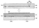
1.8 製造方法
次に、第1の実施形態に係るイメージセンサ100の製造方法について、図面を参照して詳細に説明する。図7〜図13は、第1の実施形態に係るイメージセンサの製造方法の一例を示すプロセス断面図である。1.8 Manufacturing Method Next, the manufacturing method of the
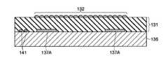
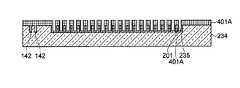
本製造方法では、図7に示すように、行列状に配列する複数のフォトダイオードPD及び転送トランジスタ111を備える半導体基板131と、単位画素110におけるその他の回路素子及び周辺回路を備える半導体基板136と、単位画素110ごとのオンチップレンズ132とを備える半導体チップが作製される。なお、半導体基板136の表面側には、引出し電極137の一部である電極パッド137Aが形成されているとよい。 In the present manufacturing method, as shown in FIG. 7, a
一方で、ガラス基板134を作製する工程では、まず、図8に示すように、ガラス基板134のベースとなるガラス基板134Aにおける1つの主面(これを裏面とする)に、溝135の開口形状と同じ形状の開口A1を持つマスクM1が形成される。マスクM1は、例えば、フォトリソグラフィにより形成された感光性レジスト膜などであってよい。また、マスクM1には、アライメントマーク142を形成するための開口A2が設けられていてもよい。 On the other hand, in the step of manufacturing the
次に、ガラス基板134AにおけるマスクM1が形成された裏面をエッチングすることで、図9に示すように、溝135及びアライメントマーク142が形成されたガラス基板134を作製する。ガラス基板134Aのエッチングには、ドライエッチングとウエットエッチングとのいずれが用いられてもよい。また、溝135及びアライメントマーク142を形成後、マスクM1は、所定の除去液等によって除去される。 Next, by etching the back surface of the
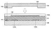
次に、図10に示すように、半導体基板131の裏面に固化前の樹脂層133Aを形成し、樹脂層133A上にガラス基板134を載置した状態で、樹脂層133Aを固化することで、半導体基板131とガラス基板134とを貼り合わせる。この貼合せでは、半導体基板131に設けられたアライメントマーク141とガラス基板134に設けられたアライメントマーク142とを用いて、両者が位置合わせされる。 Next, as shown in FIG. 10, the
なお、固化前の樹脂層133Aは、ゲル又はジェル状であってもよいし、シート状であってもよい。その際、ガラス基板134の沈み込みを抑制してエアギャップ151の寸法精度を高めるために、樹脂層133Aには高粘度の材料が用いられるとよい。ただし、粘度の低いゲル又はジェル状の樹脂層133Aを使用する場合には、有効画素領域150の周囲にスペーサを挟むことで、ガラス基板134の必要以上の沈み込みが防止されてもよい。 The
また、樹脂層133Aの固化には、加熱や紫外線照射などが用いられてもよい。その際、ガラス基板134の沈み込みを抑制してエアギャップ151の寸法精度を高めるために、固化工程を2段階以上に分けて実行してもよい。例えば、1回目の固化工程で樹脂層133Aの粘度を高め、2回目以降の固化工程で樹脂層133Aを十分に固化するようにしてもよい。 Further, heating, ultraviolet irradiation, or the like may be used to solidify the
なお、樹脂層133Aを固化する際には、ガラス基板134に対する加重をしない方が好ましいが、必要に応じて、ガラス基板134を樹脂層133Aへ押圧又は付勢してもよい。 When solidifying the
次に、図11に示すように、半導体基板131の表面側に貼り合わされた半導体基板136の裏面上に、半導体基板136の基板厚方向において電極パッド137Aと対応する領域に開口A3を有するマスクM2を形成し、このマスクM2を介して半導体基板136をエッチングすることで、半導体基板136を貫通して電極パッド137Aを露出させる開口A4を形成する。なお、マスクM2は、例えば、フォトリソグラフィにより形成された感光性レジスト膜などであってよい。また、配線層1036のエッチングには、ドライエッチングとウエットエッチングとのいずれが用いられてもよい。 Next, as shown in FIG. 11, a mask M2 having an opening A3 in a region corresponding to the
次に、図12に示すように、例えば、リフトオフなどの手法を用いることで、開口A4内部から半導体基板136の裏面の一部にかけて、電極パッド137Aと接触する導電層を形成することで、引出し電極137を形成する。 Next, as shown in FIG. 12, by using a method such as lift-off, a conductive layer is formed from the inside of the opening A4 to a part of the back surface of the
次に、図13に示すように、半導体基板136の裏面に形成された引出し電極137の一部を露出する開口A5を有するパッシベーション139を形成し、その後、開口A5から露出された引出し電極137に半田ボールなどのボールバンプ138を形成する。これにより、図6に例示するような断面構造を備えるイメージセンサ100が製造される。 Next, as shown in FIG. 13, a
1.9 作用・効果
以上のように、本実施形態では、少なくとも有効画素領域150の上方において、樹脂層133とガラス基板134との間に、真空又は気体が充填されたエアギャップ151が設けられる。これにより、半導体基板131の受光面付近における周期的な構造物(オンチップレンズ132や配線等)で反射して回折した回折光が全反射する面を、樹脂層133とエアギャップ151との境界面とすることが可能となるため、言い換えれば、回折光が全反射する面を半導体基板131の受光面に近接させることが可能となるため、回折光の受光面と平行な方向への飛行距離を短くすることが可能となる。その結果、フレア現象の発生を低減して、画質の低下を抑制することが可能となる。1.9 Actions / Effects As described above, in the present embodiment, at least above the
1.10 変形例
図14は、第1の実施形態の変形例に係るイメージセンサの断面構造例を示す断面図である。図14に例示するイメージセンサ100Aのように、ガラス基板134に形成された溝135の底面143の粗度は、ガラス基板134の他の面(例えば、ガラス基板134における半導体基板131とは反対側の面)の粗度よりも高くてもよい。例えば、底面143にモスアイ構造のような凹凸を設けることで、ガラス基板134とエアギャップ151との境界で生じる反射を低減することが可能となるため、よりフレア現象を低減して画質の低下を抑制することが可能となる。1.10 Deformation Example FIG. 14 is a cross-sectional view showing a cross-sectional structure example of an image sensor according to a modification of the first embodiment. As in the
なお、ガラス基板に形成した溝の底面の粗度を高くする構成は、第1の実施形態に限定されず、後述する他の実施形態に対しても同様に適用することが可能である。 The configuration for increasing the roughness of the bottom surface of the groove formed on the glass substrate is not limited to the first embodiment, and can be similarly applied to other embodiments described later.
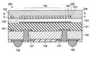
2.第2の実施形態
次に、第2の実施形態に係る固体撮像装置及び電子機器について、図面を参照して詳細に説明する。なお、以下の説明において、上述した実施形態と同様の構成については、同一の符号を付し、その重複する説明を省略する。2. 2. Second Embodiment Next, the solid-state image sensor and the electronic device according to the second embodiment will be described in detail with reference to the drawings. In the following description, the same components as those in the above-described embodiment will be designated by the same reference numerals, and duplicate description thereof will be omitted.
第2の実施形態では、第1の実施形態に係る電子機器1000において、イメージセンサ100が後述するイメージセンサ200に置き換えられている。イメージセンサ200は、図2等を用いて説明したイメージセンサ100と同様の機能構成を備える。ただし、本実施形態において、イメージセンサ200は、後述において例示するような断面構造を備える。 In the second embodiment, in the
2.1 断面構造例
図15は、第2の実施形態に係るイメージセンサの断面構造例を示す断面図である。図16は、図15におけるA−A面の一部断面構造例を示す断面図である。図17は、第2の実施形態に係るエアギャップとオンチップレンズとの位置関係の一例を示す透過図である。なお、本説明では、イメージセンサ200が裏面照射型である場合を例示するが、第1の実施形態と同様に、裏面照射型であっても表面照射型であってもよい。2.1 Cross-sectional structure example FIG. 15 is a cross-sectional view showing a cross-sectional structure example of the image sensor according to the second embodiment. FIG. 16 is a cross-sectional view showing an example of a partial cross-sectional structure of the AA plane in FIG. FIG. 17 is a transmission diagram showing an example of the positional relationship between the air gap and the on-chip lens according to the second embodiment. In this description, the case where the
図15に示すように、イメージセンサ200は、図6等を用いて説明したイメージセンサ100と同様の構成において、ガラス基板134がガラス基板234に置き換えられている。 As shown in FIG. 15, in the
図15及び図16に示すように、ガラス基板234は、第1の実施形態において図6等を用いて説明した溝135が、格子状に延在する隔壁201で複数の溝235に分割された構造を備える。すなわち、本実施形態では、第1の実施形態に係るエアギャップ151が、格子状の隔壁201によって、行列状に配列する複数のエアギャップ251に区画されている。なお、隔壁201は、半導体基板131に対してガラス基板234を支持する柱状又は壁状の構造物であってよい。 As shown in FIGS. 15 and 16, in the
また、図17に示すように、複数の溝235(すなわち、複数のエアギャップ251)は、例えば、半導体基板131を基板厚方向から見た際に、各オンチップレンズ132の光学中心が各エアギャップ251の中心と一対一に対応するように、行列状に配列している。 Further, as shown in FIG. 17, in the plurality of grooves 235 (that is, the plurality of air gaps 251), for example, when the
その際、格子状の隔壁201のうち、行方向に延びる行隔壁201aは、列方向に配列するオンチップレンズ132の境界部分211に沿って設けられ、列方向に延びる列隔壁201bは、行方向に配列するオンチップレンズ132の境界部分212に沿って設けられる。 At that time, among the grid-
行列状に配列するオンチップレンズ132の境界部分211及び212は、フォトダイオードPDの境界部分に相当する。したがって、境界部分211及び212に沿って隔壁201を設けることで、オンチップレンズ132を介してフォトダイオードPDに入射する光が隔壁201によって遮られることを低減できるため、隔壁201を設けることによる量子効率の低下を抑制することが可能となる。 The
なお、隔壁201の幅は、ガラス基板234及びイメージセンサ200について十分な物理的強度を得られる範囲内において、できるだけ狭い方が好ましい。その際、例えば、隣接するフォトダイオードPD間がDTI(Deep Trench Isolation)やFFTI(Front Full Trench Isolation)などの画素分離部によって光学的に分離されている場合には、隔壁201の幅は、その画素分離部の幅に対して、大きくても小さくてもよい。 The width of the
2.2 製造方法
次に、第2の実施形態に係るイメージセンサ200の製造方法について、図面を参照して詳細に説明する。なお、以下の説明において、第1の実施形態に係るイメージセンサ100の製造方法と同様の工程については、それを引用することで、重複する説明を省略する。図18は、第2の実施形態に係るイメージセンサの製造方法の一例を示すプロセス断面図である。2.2 Manufacturing Method Next, the manufacturing method of the
本製造方法では、まず、第1の実施形態において図7を用いて説明した工程と同様に、行列状に配列する複数のフォトダイオードPD及び転送トランジスタ111を備える半導体基板131と、単位画素110におけるその他の回路素子及び周辺回路を備える半導体基板136と、単位画素110ごとのオンチップレンズ132とを備える半導体チップが作製される。 In the present manufacturing method, first, as in the step described with reference to FIG. 7 in the first embodiment, the
一方、本実施形態では、ガラス基板234を作製する工程において、まず、ガラス基板234のベースとなるガラス基板234Aにおける1つの主面(これを裏面とする)に、溝235の開口形状と同じ形状の開口A21を持つマスクM21が形成される。マスクM21は、例えば、フォトリソグラフィにより形成された感光性レジスト膜などであってよい。また、マスクM21には、アライメントマーク142を形成するための開口A2が設けられていてもよい。 On the other hand, in the present embodiment, in the step of manufacturing the
次に、ガラス基板234AにおけるマスクM1が形成された裏面をエッチングすることで、図18に示すように、溝235及びアライメントマーク142が形成されたガラス基板234を作製する。ガラス基板234Aのエッチングには、ドライエッチングとウエットエッチングとのいずれが用いられてもよい。また、溝235及びアライメントマーク142を形成後、マスクM21は、所定の除去液等によって除去される。 Next, by etching the back surface of the
その後、第1の実施形態において、図10〜図13を用いて説明した同様の構成により、樹脂層133を用いてガラス基板234を半導体基板131に接着し、そして、引出し電極137及びボールバンプ138を形成することで、図15に例示するような断面構造を備えるイメージセンサ200が製造される。 Then, in the first embodiment, the
2.2.1 製造方法の変形例
なお、本実施形態では、第1の実施形態と同様に、半導体基板131のオンチップレンズ132が形成された裏面に樹脂層133Aを形成し、この樹脂層133Aにガラス基板234を接合する場合(図10参照)を例示したが、樹脂層133Aが形成される面は、半導体基板131側の面に限定されず、例えば、図19に例示するように、ガラス基板234における溝235が形成された面とすることも可能である。ただし、ガラス基板234における溝235が形成された面に樹脂層133Aを形成する場合、その樹脂層133Aの材料には、シート状の接着材料が用いられるとよい。2.2.1 Modifications of Manufacturing Method In this embodiment, as in the first embodiment, a
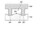
2.3 樹脂層のレンズ機能
図20は、第2の実施形態に係る樹脂層の断面構造例を示す断面図である。本実施形態のように、オンチップレンズ132に対して一対一に溝235を設けた場合、格子状の隔壁201によって押圧された状態で固化した樹脂層133は、図20に示すように、各溝235で区切られた範囲内において、中央部が盛り上がったレンズのような形状となる場合がある。そのような場合、ガラス基板234を介して各溝235内の樹脂層133に入射した光は、樹脂層133の上面202の曲率に基づいて集光することとなる。2.3 Lens function of the resin layer FIG. 20 is a cross-sectional view showing an example of a cross-sectional structure of the resin layer according to the second embodiment. When the
例えば、樹脂層133として、ゲル又はジェル状の接着材料を用いた場合や、十分に柔らかいシート状の接着材料を用いた場合には、ガラス基板234の自重や付勢力によって固化前の樹脂層133が押圧され、それにより、各溝235の中央部分がレンズのように盛り上がる。 For example, when a gel or gel-like adhesive material is used as the
そのような場合、この樹脂層133の表面の曲率も考慮し、オンチップレンズ132を透過した集光光がフォトダイオードPD内で集光するように、各オンチップレンズ132の曲率が設定されてもよい。 In such a case, the curvature of each on-
なお、樹脂層133の表面の曲率は、ガラス基板234の重量や固化前の樹脂層133の粘度や固化にかける時間や工程等を考慮して、事前に求めることが可能である。 The curvature of the surface of the
2.4 瞳補正
また、上述の説明では、オンチップレンズ132それぞれの上方に各オンチップレンズ132に一対一に対応するエアギャップ251を設けた場合を例示したが、各オンチップレンズ132と各エアギャップ251との位置関係は、例えば、像高に応じて瞳補正されてもよい。その場合、有効画素領域150の外周へ近づくにつれて、オンチップレンズ132に対するエアギャップ251の位置が有効画素領域150の中央側へシフトすることとなる。2.4 Eye correction Further, in the above description, a case where an
2.5 作用・効果
以上のように、本実施形態によれば、ガラス基板234と半導体基板131との間に、半導体基板131に対してガラス基板234を支持する柱として機能する隔壁201が設けられるため、イメージセンサ200の強度を高めて、反りなどの発生を抑制することが可能となる。2.5 Action / Effect As described above, according to the present embodiment, a
また、隔壁201の位置を隣接するオンチップレンズ132の境界部分211及び/又は212とすることで、オンチップレンズ132に入射する光が隔壁201によって遮られることも低減できるため、隔壁201を設けることによる量子効率の低下を抑制することも可能である。 Further, by setting the position of the
その他の構成、動作及び効果は、上述した実施形態と同様であってよいため、ここでは詳細な説明を省略する。 Since other configurations, operations, and effects may be the same as those in the above-described embodiment, detailed description thereof will be omitted here.
2.6 ガラス基板の変形例
つづいて、ガラス基板234の変形例について、幾つか例を挙げて説明する。2.6 Deformation Example of Glass Substrate Next, some modification examples of the
2.6.1 第1変形例
図21は、第1変形例に係るガラス基板の概略構成例を示す断面図である。なお、図21には、図16と同様に、図15におけるA−A面の一部断面構造例が示されている。2.6.1 First Modified Example FIG. 21 is a cross-sectional view showing a schematic configuration example of a glass substrate according to the first modified example. Note that FIG. 21 shows an example of a partial cross-sectional structure of the AA plane in FIG. 15 as in FIG.
図21に示すように、ガラス基板234Aでは、ガラス基板234における矩形の溝235(すなわち、エアギャップ251)が、円形の溝235A(すなわち、素子形成面と平行な面の形状が円形のエアギャップ251A)に置き換えられている。 As shown in FIG. 21, in the
このような円形のエアギャップ251Aによっても、第2の実施形態と同様に、ガラス基板234A及びイメージセンサ200の強度を向上させつつ、フレア現象による画質の低下を抑制することが可能となる。 Even with such a
また、半導体基板131の基板厚方向において、エアギャップ251Aの中心とオンチップレンズ132の中心とを位置合わせすることで、オンチップレンズ132に入射する光が隔壁201Aによって遮られることも低減できるため、隔壁201を設けることによる量子効率の低下を抑制することも可能である。 Further, by aligning the center of the
なお、素子形成面と平行な面の形状は、円形に限られず、楕円形や三角形以上の多角形など、種々変形することが可能である。 The shape of the surface parallel to the element forming surface is not limited to a circle, and can be variously deformed such as an ellipse or a polygon having a triangle or more.
2.6.2 第2変形例
図22は、第2変形例に係るエアギャップとオンチップレンズとの対応関係の一例を示す透過図である。2.6.2 Second Modified Example FIG. 22 is a transmission diagram showing an example of the correspondence between the air gap and the on-chip lens according to the second modified example.
上述した第2の実施形態では、1つのオンチップレンズ132に対して1つの溝235(すなわち、エアギャップ251)が対応するように、行隔壁201a及び列隔壁201bを設けられた場合を例示したが、このような構成に限定されるものではない。例えば、図22に例示するガラス基板235Bのように、複数(図22では、2×2の計4つ)のオンチップレンズ132に対して1つの溝235bが対応するように、言い換えれば、行列状に配列する複数のオンチップレンズを複数(図22では、2×2の計4つ)のオンチップレンズ132ごとに区画するように、行隔壁201a及び列隔壁201bが設けられてもよい。 In the second embodiment described above, the case where the
このような構成によっても、第2の実施形態と同様に、ガラス基板234B及びイメージセンサ200の強度を向上させつつ、フレア現象による画質の低下を抑制することが可能となる。 Even with such a configuration, it is possible to suppress deterioration of image quality due to the flare phenomenon while improving the strength of the
なお、行隔壁201a及び列隔壁201bによって区画されるフォトダイオードPDの数は、2×2の計4つに限定されず、m(mは1以上の整数)×n(nは1以上の整数)個であってよい。 The number of photodiode PDs partitioned by the
2.6.3 第3変形例
図23は、第3変形例に係るガラス基板の概略構成例を示す断面図である。なお、図23には、図15におけるA−A面の断面構造例が示されている。2.6.3 Third Modified Example FIG. 23 is a cross-sectional view showing a schematic configuration example of a glass substrate according to the third modified example. Note that FIG. 23 shows an example of the cross-sectional structure of the AA plane in FIG.
図23に示すように、イメージセンサ200の強度を維持するためにガラス基板234Cに設ける隔壁201は、少なくとも1本あればよい。 As shown in FIG. 23, at least one
例えば、第1の実施形態に係るエアギャップ151を分断するように、少なくとも1本の隔壁201を設けることで、第2の実施形態と同様に、ガラス基板234C及びイメージセンサ200の強度を向上させつつ、フレア現象による画質の低下を抑制することが可能となる。 For example, by providing at least one
2.6.4 第4変形例
図24は、第4変形例に係るイメージセンサの断面構造例を示す断面図である。なお、図24には、図15に示す断面に対応する断面が示されている。2.6.4 Fourth Modified Example FIG. 24 is a cross-sectional view showing a cross-sectional structure example of the image sensor according to the fourth modified example. Note that FIG. 24 shows a cross section corresponding to the cross section shown in FIG.
図24に例示するイメージセンサ200Dのように、半導体基板131に対してガラス基板234Dを支持する隔壁201Dは、樹脂層233を用いて構成されてもよい。 Like the
このような構成によっても、第2の実施形態と同様に、ガラス基板234D及びイメージセンサ200の強度を向上させつつ、フレア現象による画質の低下を抑制することが可能となる。 Even with such a configuration, it is possible to suppress deterioration of image quality due to the flare phenomenon while improving the strength of the
なお、樹脂層233による隔壁201Dは、例えば、樹脂層233の上層(ガラス基板234D側)と下層(半導体基板131側)とで異なる樹脂層を用い、上層の樹脂層を溝235の開口パターンと同形状のパターンで露光して固化することで、形成することが可能である。 For the
3.第3の実施形態
次に、第3の実施形態に係る固体撮像装置及び電子機器について、図面を参照して詳細に説明する。なお、以下の説明において、上述した実施形態と同様の構成については、同一の符号を付し、その重複する説明を省略する。3. 3. Third Embodiment Next, the solid-state image sensor and the electronic device according to the third embodiment will be described in detail with reference to the drawings. In the following description, the same components as those in the above-described embodiment will be designated by the same reference numerals, and duplicate description thereof will be omitted.
第3の実施形態では、第1の実施形態に係る電子機器1000において、イメージセンサ100が後述するイメージセンサ300に置き換えられている。イメージセンサ300は、例えば、第1の実施形態において図2等を用いて説明したイメージセンサ100と同様の機能構成を備える。ただし、本実施形態において、イメージセンサ300は、後述において例示するような断面構造を備える。 In the third embodiment, in the
3.1 断面構造例
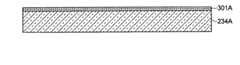
図25は、第3の実施形態に係るイメージセンサの断面構造例を示す断面図である。なお、本説明では、イメージセンサ300が裏面照射型である場合を例示するが、第1の実施形態と同様に、裏面照射型であっても表面照射型であってもよい。3.1 Cross-sectional structure example FIG. 25 is a cross-sectional view showing a cross-sectional structure example of the image sensor according to the third embodiment. In this description, the case where the
図25に示すように、イメージセンサ300は、第2の実施形態において図15等を用いて説明したイメージセンサ200と同様の構成において、ガラス基板234における樹脂層133と接触する面に、遮光膜301が設けられている。 As shown in FIG. 25, the
遮光膜301の材料には、例えば、タングステン(W)、チタン(Ti)、カーボンレジストなど、可視光を遮光する特性を備える材料を用いることができる。 As the material of the light-shielding
また、本実施形態における隔壁201は、第2の実施形態において説明したように、隣接するオンチップレンズ132の境界部分211及び212に配置されている。 Further, the
このような構成とすることで、ある単位画素110に対応するエアギャップ251に入射した光が隣接する単位画素110に対応するオンチップレンズ132へ入射する、いわゆる隣接画素への光の漏れ込みを低減することが可能となる。それにより、イメージセンサ300の画素分離特性を向上して混色を低減することが可能となるため、画質の低下を抑制することが可能となる。 With such a configuration, the light incident on the
3.2 製造方法
次に、第3の実施形態に係るイメージセンサ300の製造方法について、図面を参照して詳細に説明する。なお、以下の説明において、第1又は第2の実施形態に係るイメージセンサ100又は200の製造方法と同様の工程については、それを引用することで、重複する説明を省略する。図26及び図27は、第3の実施形態に係るイメージセンサの製造方法の一例を示すプロセス断面図である。3.2 Manufacturing Method Next, the manufacturing method of the
本製造方法では、まず、第1の実施形態において図7を用いて説明した工程と同様に、行列状に配列する複数のフォトダイオードPD及び転送トランジスタ111を備える半導体基板131と、単位画素110におけるその他の回路素子及び周辺回路を備える半導体基板136と、単位画素110ごとのオンチップレンズ132とを備える半導体チップが作製される。 In the present manufacturing method, first, as in the step described with reference to FIG. 7 in the first embodiment, the
一方、本実施形態では、ガラス基板234を作製する工程においては、図26に示すように、まず、ガラス基板234のベースとなるガラス基板234Aにおける1つの主面(これを裏面とする)に、遮光膜301Aが形成される。 On the other hand, in the present embodiment, as shown in FIG. 26, in the step of manufacturing the
次に、遮光膜301A上に、溝235の開口形状と同じ形状の開口A21を持つマスクM21が形成される。マスクM21の形成は、第2の実施形態において図18を用いて説明した工程と同様であってよい。 Next, a mask M21 having an opening A21 having the same shape as the opening of the
次に、ガラス基板234AにおけるマスクM1が形成された裏面をエッチングすることで、図27に示すように、溝235及びアライメントマーク142を備え、少なくとも隔壁201の底面に遮光膜301が形成されたガラス基板234を作製する。ガラス基板234Aのエッチングには、第2の実施形態において図18を用いて説明した工程と同様であってよい。また、溝235、アライメントマーク142及び遮光膜301を形成後、マスクM21は、所定の除去液等によって除去される。 Next, by etching the back surface of the
その後、第1の実施形態において、図10〜図13を用いて説明した同様の構成により、樹脂層133を用いてガラス基板234を半導体基板131に接着し、そして、引出し電極137及びボールバンプ138を形成することで、図25に例示するような断面構造を備えるイメージセンサ300が製造される。 Then, in the first embodiment, the
3.3 作用・効果
以上のように、第3の実施形態によれば、少なくとも有効画素領域150内の隔壁201の底面に、遮光膜301が設けられる。これにより、ある単位画素110に対応するエアギャップ251に入射した光が隣接する単位画素110に対応するオンチップレンズ132へ入射する、いわゆる隣接画素への光の漏れ込みを低減することが可能となるため、イメージセンサ300の画素分離特性を向上して混色を低減することが可能となり、それにより、画質の低下を抑制することが可能となる。3.3 Actions / Effects As described above, according to the third embodiment, the light-shielding
なお、本実施形態では、第2の実施形態に係るイメージセンサ200をベースとした場合を例示したが、ベースとする実施形態は、第2の実施形態に限定されず、その変形例や第1の実施形態など、他の実施形態又はその変形例とすることも可能である。 In this embodiment, the case where the
また、その他の構成、動作及び効果は、上述した実施形態と同様であってよいため、ここでは詳細な説明を省略する。 Further, since other configurations, operations and effects may be the same as those in the above-described embodiment, detailed description thereof will be omitted here.
4.第4の実施形態
次に、第4の実施形態に係る固体撮像装置及び電子機器について、図面を参照して詳細に説明する。なお、以下の説明において、上述した実施形態と同様の構成については、同一の符号を付し、その重複する説明を省略する。4. Fourth Embodiment Next, the solid-state image sensor and the electronic device according to the fourth embodiment will be described in detail with reference to the drawings. In the following description, the same components as those in the above-described embodiment will be designated by the same reference numerals, and duplicate description thereof will be omitted.
第4の実施形態では、第1の実施形態に係る電子機器1000において、イメージセンサ100が後述するイメージセンサ400に置き換えられている。イメージセンサ400は、例えば、第1の実施形態において図2等を用いて説明したイメージセンサ100と同様の機能構成を備える。ただし、本実施形態において、イメージセンサ400は、後述において例示するような断面構造を備える。 In the fourth embodiment, in the
4.1 断面構造例
図28は、第4の実施形態に係るイメージセンサの断面構造例を示す断面図である。なお、本説明では、イメージセンサ400が裏面照射型である場合を例示するが、第1の実施形態と同様に、裏面照射型であっても表面照射型であってもよい。4.1 Cross-sectional structure example FIG. 28 is a cross-sectional view showing a cross-sectional structure example of the image sensor according to the fourth embodiment. In this description, the case where the
図28に示すように、イメージセンサ400は、第3の実施形態において図25等を用いて説明したイメージセンサ300と同様の構成において、ガラス基板234における隔壁201の底面に加え、隔壁201の側面にも、遮光膜401が設けられている。 As shown in FIG. 28, the
遮光膜401の材料には、第3の実施形態に係る遮光膜301と同様に、例えば、タングステン(W)、チタン(Ti)、カーボンレジストなど、可視光を遮光する特性を備える材料を用いることができる。 As the material of the light-shielding
また、本実施形態における隔壁201は、第2の実施形態において説明したように、隣接するオンチップレンズ132の境界部分211及び212に配置されている。 Further, the
このような構成とすることで、隣接画素への光の漏れ込みをより低減することが可能となる。それにより、イメージセンサ400の画素分離特性をより向上して混色をさらに低減することが可能となるため、画質の低下をさらに抑制することが可能となる。 With such a configuration, it is possible to further reduce the leakage of light to adjacent pixels. As a result, it is possible to further improve the pixel separation characteristics of the
4.2 製造方法
次に、第4の実施形態に係るイメージセンサ400の製造方法について、図面を参照して詳細に説明する。なお、以下の説明において、上述した実施形態に係るイメージセンサ100、100A、200、200D又は300の製造方法と同様の工程については、それを引用することで、重複する説明を省略する。図29及び図30は、第4の実施形態に係るイメージセンサの製造方法の一例を示すプロセス断面図である。4.2 Manufacturing Method Next, the manufacturing method of the
本製造方法では、まず、第1の実施形態において図7を用いて説明した工程と同様に、行列状に配列する複数のフォトダイオードPD及び転送トランジスタ111を備える半導体基板131と、単位画素110におけるその他の回路素子及び周辺回路を備える半導体基板136と、単位画素110ごとのオンチップレンズ132とを備える半導体チップが作製される。 In the present manufacturing method, first, as in the step described with reference to FIG. 7 in the first embodiment, the
一方、ガラス基板234を作製する工程においては、第2の実施形態において図18を用いて説明した工程と同様の工程により、裏面に溝235が形成されたガラス基板234が形成される。 On the other hand, in the step of producing the
次に、例えば、スパッタリングやCVD(Chemical Vapor Deposition)などの成膜技術を用いることで、図29に示すように、ガラス基板234の溝235が形成された面に、タングステン(W)などによる遮光膜401Aを形成する。その際、溝235の側面(すなわち、隔壁201の側面)及び底面にも、遮光膜401Aが形成される。 Next, for example, by using a film forming technique such as sputtering or CVD (Chemical Vapor Deposition), as shown in FIG. 29, the surface of the
次に、例えば、ガラス基板234における遮光膜401Aが形成された面を全面エッチバックすることで、溝235の底面に形成された遮光膜401Aを除去して、隔壁201の上面と側面に遮光膜401を形成する。その際、隔壁201上面の遮光膜401は、薄膜化されてもよい。 Next, for example, by etching back the entire surface of the
その後、第1の実施形態において、図10〜図13を用いて説明した同様の構成により、樹脂層133を用いてガラス基板234を半導体基板131に接着し、そして、引出し電極137及びボールバンプ138を形成することで、図28に例示するような断面構造を備えるイメージセンサ400が製造される。 Then, in the first embodiment, the
4.2.1 製造方法の変形例
なお、上述では、全面エッチバックにより遮光膜401Aを遮光膜401に加工する場合を例示したが、このような手法に限定されず、例えば、図31に例示するように、隔壁201の上面及び側面の遮光膜401A上に、遮光膜401Aの窪みの開口と同様の開口形状A41を有するマスクM41を形成し、その状態で溝235底部の遮光膜401AをRIE(Reactive Ion Etching)などにより除去することで、遮光膜401Aを遮光膜401に加工してもよい。なお、マスクM41の形成には、フォトリソグラフィなどの技術を用いることができる。4.2.1 Modification of Manufacturing Method In the above, the case where the light-shielding
4.3 作用・効果
以上のように、第4の実施形態によれば、少なくとも有効画素領域150内の隔壁201の底面及び側壁に、遮光膜301が設けられる。これにより、隣接画素への光の漏れ込みをより低減することが可能となるため、イメージセンサ400の画素分離特性をより向上して混色をさらに低減することが可能となる。それにより、画質の低下をさらに抑制することが可能となる。4.3 Actions / Effects As described above, according to the fourth embodiment, the light-shielding
なお、本実施形態では、第3の実施形態に係るイメージセンサ300をベースとした場合を例示したが、ベースとする実施形態は、第3の実施形態に限定されず、その変形例や第1又は第2の実施形態など、他の実施形態又はその変形例とすることも可能である。 In the present embodiment, the case where the
また、その他の構成、動作及び効果は、上述した実施形態と同様であってよいため、ここでは詳細な説明を省略する。 Further, since other configurations, operations and effects may be the same as those in the above-described embodiment, detailed description thereof will be omitted here.
5.第5の実施形態
次に、第5の実施形態に係る固体撮像装置及び電子機器について、図面を参照して詳細に説明する。なお、以下の説明において、上述した実施形態と同様の構成については、同一の符号を付し、その重複する説明を省略する。5. Fifth Embodiment Next, the solid-state image sensor and the electronic device according to the fifth embodiment will be described in detail with reference to the drawings. In the following description, the same components as those in the above-described embodiment will be designated by the same reference numerals, and duplicate description thereof will be omitted.
第5の実施形態では、第1の実施形態に係る電子機器1000において、イメージセンサ100が後述するイメージセンサ500に置き換えられている。イメージセンサ500は、例えば、第1の実施形態において図2等を用いて説明したイメージセンサ100と同様の機能構成を備える。ただし、本実施形態において、イメージセンサ500は、後述において例示するような断面構造を備える。 In the fifth embodiment, in the
5.1 断面構造例
図32は、第5の実施形態に係るイメージセンサの断面構造例を示す断面図である。なお、本説明では、イメージセンサ500が裏面照射型である場合を例示するが、第1の実施形態と同様に、裏面照射型であっても表面照射型であってもよい。5.1 Cross-sectional structure example FIG. 32 is a cross-sectional view showing a cross-sectional structure example of the image sensor according to the fifth embodiment. In this description, the case where the
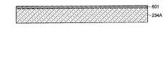
図32に示すように、イメージセンサ500は、第4の実施形態において図28等を用いて説明したイメージセンサ400と同様の構成において、ガラス基板234における溝235が形成された面と反対側の面に、反射防止膜501が設けられている。 As shown in FIG. 32, the
反射防止膜501は、例えば、シリコン酸化膜(SiO2膜)と窒化チタン膜(TiN)とが交互に積層された誘電体多層膜など、少なくとも可視光を高効率で透過させる種々の反射防止膜であってよい。The
このように、光の入射面であるガラス基板234の上面に反射防止膜501を設けることで、ガラス基板234の上面で反射する光を低減して入射効率を高めることが可能となる。それにより、各単位画素110のフォトダイオードPDに入射する光量を増加させてコントラストを高めることが可能となるため、画質の低下をさらに抑制することが可能となる。 In this way, by providing the
5.2 製造方法
次に、第5の実施形態に係るイメージセンサ500の製造方法について、図面を参照して詳細に説明する。なお、以下の説明において、上述した実施形態に係るイメージセンサ100、100A、200、200D、300又は400の製造方法と同様の工程については、それを引用することで、重複する説明を省略する。図33は、第5の実施形態に係るイメージセンサの製造方法の一例を示すプロセス断面図である。5.2 Manufacturing Method Next, the manufacturing method of the
本製造方法では、まず、第1の実施形態において図7を用いて説明した工程と同様に、行列状に配列する複数のフォトダイオードPD及び転送トランジスタ111を備える半導体基板131と、単位画素110におけるその他の回路素子及び周辺回路を備える半導体基板136と、単位画素110ごとのオンチップレンズ132とを備える半導体チップが作製される。 In the present manufacturing method, first, as in the step described with reference to FIG. 7 in the first embodiment, the
一方、ガラス基板234を作製する工程においては、図33に示すように、まず、ガラス基板234Aの上面(溝235が形成される面と反対側の面)上に、反射防止膜501が形成される。反射防止膜501の成膜には、一般的な成膜技術が用いられてよい。 On the other hand, in the step of manufacturing the
次に、第2の実施形態において図18を用いて説明した工程と同様の工程により、裏面に溝235が形成されたガラス基板234を作製し、つづいて、溝235の側面(すなわち、隔壁201の側面)及び底面に遮光膜401を形成する。 Next, a
その後、第1の実施形態において、図10〜図13を用いて説明した同様の構成により、樹脂層133を用いてガラス基板234を半導体基板131に接着し、そして、引出し電極137及びボールバンプ138を形成することで、図32に例示するような断面構造を備えるイメージセンサ500が製造される。 Then, in the first embodiment, the
5.3 作用・効果
以上のように、第5の実施形態によれば、光の入射面であるガラス基板234の上面に反射防止膜501が設けられる。これにより、ガラス基板234の上面で反射する光を低減して入射効率を高めることが可能となるため、各単位画素110のフォトダイオードPDに入射する光量を増加させてコントラストを高めることが可能となる。それにより、画質の低下をさらに抑制することが可能となる。5.3 Action / Effect As described above, according to the fifth embodiment, the
なお、本実施形態では、第4の実施形態に係るイメージセンサ400をベースとした場合を例示したが、ベースとする実施形態は、第4の実施形態に限定されず、その変形例や第1、第2又は第3の実施形態など、他の実施形態又はその変形例とすることも可能である。 In this embodiment, the case where the
また、その他の構成、動作及び効果は、上述した実施形態と同様であってよいため、ここでは詳細な説明を省略する。 Further, since other configurations, operations and effects may be the same as those in the above-described embodiment, detailed description thereof will be omitted here.
6.第6の実施形態
第5の実施形態では、ガラス基板234の上面に、誘電体多層膜などによる反射防止膜501を設けた場合を例示したが、ガラス基板234の上面に配置する膜は、反射防止膜501に限定されず、種々変更することが可能である。6. Sixth Embodiment In the fifth embodiment, the case where the
そこで第6の実施形態では、ガラス基板234の上面に配置する膜を、反射防止膜501に代えて、赤外光を遮断するカラーフィルタ(以下、IRカットフィルタという)とした場合について、例を挙げて説明する。 Therefore, in the sixth embodiment, an example is taken in the case where the film arranged on the upper surface of the
なお、以下の説明において、上述した実施形態と同様の構成については、同一の符号を付し、その重複する説明を省略する。 In the following description, the same components as those in the above-described embodiment will be designated by the same reference numerals, and duplicate description thereof will be omitted.
6.1 断面構造例
図34は、第6の実施形態に係るイメージセンサの断面構造例を示す断面図である。なお、本説明では、イメージセンサ600が裏面照射型である場合を例示するが、第1の実施形態と同様に、裏面照射型であっても表面照射型であってもよい。6.1 Cross-sectional structure example FIG. 34 is a cross-sectional view showing a cross-sectional structure example of the image sensor according to the sixth embodiment. In this description, the case where the
図34に示すように、イメージセンサ600は、第4の実施形態において図28等を用いて説明したイメージセンサ400と同様の構成において、ガラス基板234における溝235が形成された面と反対側の面に、IRカットフィルタ601が設けられている。 As shown in FIG. 34, the
IRカットフィルタ601は、例えば、赤外光又は近赤外光に対する吸収率が高い材料を用いて形成された膜であってよい。 The IR cut
このように、光の入射面であるガラス基板234の上面にIRカットフィルタ601を設けることで、赤外光の入射によるノイズを低減することが可能となるため、画質の低下をさらに抑制することが可能となる。 In this way, by providing the IR cut
6.2 製造方法
次に、第6の実施形態に係るイメージセンサ600の製造方法について、図面を参照して詳細に説明する。なお、以下の説明において、上述した実施形態に係るイメージセンサ100、100A、200、200D、300、400又は500の製造方法と同様の工程については、それを引用することで、重複する説明を省略する。図35は、第6の実施形態に係るイメージセンサの製造方法の一例を示すプロセス断面図である。6.2 Manufacturing Method Next, the manufacturing method of the
本製造方法では、まず、第1の実施形態において図7を用いて説明した工程と同様に、行列状に配列する複数のフォトダイオードPD及び転送トランジスタ111を備える半導体基板131と、単位画素110におけるその他の回路素子及び周辺回路を備える半導体基板136と、単位画素110ごとのオンチップレンズ132とを備える半導体チップが作製される。 In the present manufacturing method, first, as in the step described with reference to FIG. 7 in the first embodiment, the
一方、ガラス基板234を作製する工程においては、図35に示すように、まず、ガラス基板234Aの上面(溝235が形成される面と反対側の面)上に、IRカットフィルタ601が形成される。IRカットフィルタ601の成膜には、一般的な成膜技術が用いられてよい。 On the other hand, in the step of manufacturing the
次に、第2の実施形態において図18を用いて説明した工程と同様の工程により、裏面に溝235が形成されたガラス基板234を作製し、つづいて、溝235の側面(すなわち、隔壁201の側面)及び底面に遮光膜401を形成する。 Next, a
その後、第1の実施形態において、図10〜図13を用いて説明した同様の構成により、樹脂層133を用いてガラス基板234を半導体基板131に接着し、そして、引出し電極137及びボールバンプ138を形成することで、図34に例示するような断面構造を備えるイメージセンサ600が製造される。 Then, in the first embodiment, the
6.3 作用・効果
以上のように、第6の実施形態によれば、光の入射面であるガラス基板234の上面にIRカットフィルタ601が設けられる。これにより、赤外光の入射によるノイズを低減することが可能となるため、画質の低下をさらに抑制することが可能となる。6.3 Action / Effect As described above, according to the sixth embodiment, the IR cut
なお、本実施形態では、第4の実施形態に係るイメージセンサ400をベースとした場合を例示したが、ベースとする実施形態は、第4の実施形態に限定されず、その変形例や第1、第2、第3又は第5の実施形態など、他の実施形態又はその変形例とすることも可能である。 In this embodiment, the case where the
また、その他の構成、動作及び効果は、上述した実施形態と同様であってよいため、ここでは詳細な説明を省略する。 Further, since other configurations, operations and effects may be the same as those in the above-described embodiment, detailed description thereof will be omitted here.
以上、本開示の実施形態について説明したが、本開示の技術的範囲は、上述の実施形態そのままに限定されるものではなく、本開示の要旨を逸脱しない範囲において種々の変更が可能である。また、異なる実施形態及び変形例にわたる構成要素を適宜組み合わせてもよい。 Although the embodiments of the present disclosure have been described above, the technical scope of the present disclosure is not limited to the above-described embodiments as they are, and various changes can be made without departing from the gist of the present disclosure. In addition, components covering different embodiments and modifications may be combined as appropriate.
また、本明細書に記載された各実施形態における効果はあくまで例示であって限定されるものでは無く、他の効果があってもよい。 Further, the effects in each of the embodiments described in the present specification are merely examples and are not limited, and other effects may be obtained.
なお、本技術は以下のような構成も取ることができる。
(1)
受光素子を備える半導体基板と、
前記半導体基板の第1面に配置されたオンチップレンズと、
前記オンチップレンズを覆う樹脂層と、
前記半導体基板の前記第1面側に前記樹脂層と離間して配置されたガラス基板と、
を備える固体撮像装置。
(2)
前記半導体基板に対して前記ガラス基板を支持する壁状の構造物をさらに備える前記(1)に記載の固体撮像装置。
(3)
前記半導体基板は、前記半導体基板における前記第1面側に行列状に配置された複数の前記受光素子を備え、
前記構造物は、隣接する前記受光素子の境界部分に配置されている
前記(2)に記載の固体撮像装置。
(4)
前記ガラス基板は、前記半導体基板と対向する面に第1溝を有し、
前記構造物は、前記第1溝を複数の第2溝に区画する
前記(2)又は(3)に記載の固体撮像装置。
(5)
前記構造物は、前記ガラス基板の一部であり、前記第1溝を前記複数の第2溝に区画する隔壁である前記(4)に記載の固体撮像装置。
(6)
前記オンチップレンズは、前記受光素子それぞれと一対一に対応し、
前記構造物は、前記第2溝が前記オンチップレンズと一対一に対応するように、前記第1溝を前記複数の第2溝に区画する
前記(4)又は(5)に記載の固体撮像装置。
(7)
前記オンチップレンズは、前記受光素子それぞれと一対一に対応し、
前記構造物は、前記第2溝と複数の前記オンチップレンズとが一対一に対応するように、前記第1溝を前記複数の第2溝に区画する
前記(4)又は(5)に記載の固体撮像装置。
(8)
前記第1溝の深さは、1μm(マイクロメートル)以上であって、前記ガラス基板の最大の厚さの半分以下の深さである前記(4)又は(5)に記載の固体撮像装置。
(9)
前記構造物における前記半導体基板側の面に設けられた第1遮光膜をさらに備える前記(2)〜(7)の何れか1項に記載の固体撮像装置。
(10)
前記構造物の側面に設けられた第2遮光膜をさらに備える前記(9)に記載の固体撮像装置。
(11)
前記ガラス基板における前記半導体基板と対向する面と反対側の面に設けられた反射防止膜をさらに備える前記(1)〜(10)の何れか1項に記載の固体撮像装置。
(12)
前記ガラス基板における前記半導体基板と対向する面と反対側の面に設けられ、赤外光を吸収するフィルタをさらに備える前記(1)〜(10)の何れか1項に記載の固体撮像装置。
(13)
前記ガラス基板における前記半導体基板と対向する面の粗度は、当該ガラス基板における前記半導体基板とは反対側の面の粗度よりも高い前記(1)〜(12)の何れか1項に記載の固体撮像装置。
(14)
前記樹脂層は、前記第2溝それぞれの内部へ向けて盛り上がっている前記(4)又は(5)に記載の固体撮像装置。
(15)
前記第2溝の前記第1面と平行な面の断面形状は、矩形である前記(4)又は(5)に記載の固体撮像装置。
(16)
前記第2溝の前記第1面と平行な面の断面形状は、円形である前記(4)又は(5)に記載の固体撮像装置。
(17)
固体撮像装置と、
入射光を前記固体撮像装置の受光面に結像する光学系と、
前記固体撮像装置を制御するプロセッサと、
を備え、
前記固体撮像装置は、
受光素子を備える半導体基板と、
前記半導体基板の第1面に配置されたオンチップレンズと、
前記オンチップレンズを覆う樹脂層と、
前記半導体基板の前記第1面側に前記樹脂層と離間して配置されたガラス基板と、
を備える電子機器。The present technology can also have the following configurations.
(1)
A semiconductor substrate equipped with a light receiving element and
An on-chip lens arranged on the first surface of the semiconductor substrate and
The resin layer covering the on-chip lens and
A glass substrate arranged on the first surface side of the semiconductor substrate so as to be separated from the resin layer,
A solid-state image sensor.
(2)
The solid-state image sensor according to (1), further comprising a wall-shaped structure that supports the glass substrate with respect to the semiconductor substrate.
(3)
The semiconductor substrate includes a plurality of the light receiving elements arranged in a matrix on the first surface side of the semiconductor substrate.
The solid-state imaging device according to (2), wherein the structure is arranged at a boundary portion of an adjacent light receiving element.
(4)
The glass substrate has a first groove on a surface facing the semiconductor substrate.
The solid-state image sensor according to (2) or (3) above, wherein the structure divides the first groove into a plurality of second grooves.
(5)
The solid-state image sensor according to (4), wherein the structure is a part of the glass substrate and is a partition wall that divides the first groove into the plurality of second grooves.
(6)
The on-chip lens has a one-to-one correspondence with each of the light receiving elements.
The solid-state imaging according to (4) or (5) above, wherein the structure divides the first groove into the plurality of second grooves so that the second groove has a one-to-one correspondence with the on-chip lens. apparatus.
(7)
The on-chip lens has a one-to-one correspondence with each of the light receiving elements.
The structure is described in (4) or (5) above, wherein the first groove is partitioned into the plurality of second grooves so that the second groove and the plurality of on-chip lenses have a one-to-one correspondence with each other. Solid-state image sensor.
(8)
The solid-state image sensor according to (4) or (5), wherein the depth of the first groove is 1 μm (micrometer) or more and less than half the maximum thickness of the glass substrate.
(9)
The solid-state image sensor according to any one of (2) to (7) above, further comprising a first light-shielding film provided on the surface of the structure on the semiconductor substrate side.
(10)
The solid-state image sensor according to (9) above, further comprising a second light-shielding film provided on the side surface of the structure.
(11)
The solid-state image sensor according to any one of (1) to (10) above, further comprising an antireflection film provided on a surface of the glass substrate opposite to the surface facing the semiconductor substrate.
(12)
The solid-state image sensor according to any one of (1) to (10) above, which is provided on a surface of the glass substrate opposite to the surface facing the semiconductor substrate and further includes a filter that absorbs infrared light.
(13)
Item 2. The item (1) to (12), wherein the roughness of the surface of the glass substrate facing the semiconductor substrate is higher than the roughness of the surface of the glass substrate opposite to the semiconductor substrate. Solid-state image sensor.
(14)
The solid-state image sensor according to (4) or (5), wherein the resin layer is raised toward the inside of each of the second grooves.
(15)
The solid-state image sensor according to (4) or (5), wherein the cross-sectional shape of the surface of the second groove parallel to the first surface is rectangular.
(16)
The solid-state image sensor according to (4) or (5), wherein the cross-sectional shape of the surface of the second groove parallel to the first surface is circular.
(17)
Solid-state image sensor and
An optical system that forms an image of incident light on the light receiving surface of the solid-state image sensor,
A processor that controls the solid-state image sensor,
With
The solid-state image sensor
A semiconductor substrate equipped with a light receiving element and
An on-chip lens arranged on the first surface of the semiconductor substrate and
The resin layer covering the on-chip lens and
A glass substrate arranged on the first surface side of the semiconductor substrate so as to be separated from the resin layer,
Electronic equipment equipped with.
100、100A、200、200D、300、400、500、600 固体撮像装置(イメージセンサ)
101 画素アレイ部
102 垂直駆動回路
103 カラム処理回路
104 水平駆動回路
105 システム制御部
108 信号処理部
109 データ格納部
110 単位画素
111 転送トランジスタ
112 リセットトランジスタ
113 増幅トランジスタ
114 選択トランジスタ
121 受光チップ
122 回路チップ
131、136 半導体基板
132 オンチップレンズ
133、133A、233 樹脂層
134、134A、234、234A、234B、234C ガラス基板
135、235、235A、235b 溝
137 引出し電極
137A 電極パッド
138 ボールバンプ
139 パッシベーション
141、142 アライメントマーク
143 底面
150 有効画素領域
151、251、251A エアギャップ
201、201A、201D 隔壁
201a 行隔壁
201b 列隔壁
202 上面
211、212 境界部分
301、301A、401、401A 遮光膜
501 反射防止膜
601 IRカットフィルタ
1000 電子機器
1020 撮像レンズ
1030 記憶部
1040 プロセッサ
FD 浮遊拡散層
LD 画素駆動線
LD111 転送トランジスタ駆動線
LD112 リセットトランジスタ駆動線
LD114 選択トランジスタ駆動線
PD フォトダイオード
VSL 垂直信号線100, 100A, 200, 200D, 300, 400, 500, 600 Solid-state image sensor (image sensor)
101
Claims (17)
Translated fromJapanese前記半導体基板の第1面に配置されたオンチップレンズと、
前記オンチップレンズを覆う樹脂層と、
前記半導体基板の前記第1面側に前記樹脂層と離間して配置されたガラス基板と、
を備える固体撮像装置。A semiconductor substrate equipped with a light receiving element and
An on-chip lens arranged on the first surface of the semiconductor substrate and
The resin layer covering the on-chip lens and
A glass substrate arranged on the first surface side of the semiconductor substrate so as to be separated from the resin layer,
A solid-state image sensor.
前記構造物は、隣接する前記受光素子の境界部分に配置されている
請求項2に記載の固体撮像装置。The semiconductor substrate includes a plurality of the light receiving elements arranged in a matrix on the first surface side of the semiconductor substrate.
The solid-state imaging device according to claim 2, wherein the structure is arranged at a boundary portion of the adjacent light receiving element.
前記構造物は、前記第1溝を複数の第2溝に区画する
請求項3に記載の固体撮像装置。The glass substrate has a first groove on a surface facing the semiconductor substrate.
The solid-state image sensor according to claim 3, wherein the structure is a partition of the first groove into a plurality of second grooves.
前記構造物は、前記第2溝が前記オンチップレンズと一対一に対応するように、前記第1溝を前記複数の第2溝に区画する
請求項4に記載の固体撮像装置。The on-chip lens has a one-to-one correspondence with each of the light receiving elements.
The solid-state image sensor according to claim 4, wherein the structure divides the first groove into a plurality of second grooves so that the second groove has a one-to-one correspondence with the on-chip lens.
前記構造物は、前記第2溝と複数の前記オンチップレンズとが一対一に対応するように、前記第1溝を前記複数の第2溝に区画する
請求項4に記載の固体撮像装置。The on-chip lens has a one-to-one correspondence with each of the light receiving elements.
The solid-state image sensor according to claim 4, wherein the structure divides the first groove into the plurality of second grooves so that the second groove and the plurality of on-chip lenses have a one-to-one correspondence.
入射光を前記固体撮像装置の受光面に結像する光学系と、
前記固体撮像装置を制御するプロセッサと、
を備え、
前記固体撮像装置は、
受光素子を備える半導体基板と、
前記半導体基板の第1面に配置されたオンチップレンズと、
前記オンチップレンズを覆う樹脂層と、
前記半導体基板の前記第1面側に前記樹脂層と離間して配置されたガラス基板と、
を備える電子機器。Solid-state image sensor and
An optical system that forms an image of incident light on the light receiving surface of the solid-state image sensor,
A processor that controls the solid-state image sensor,
With
The solid-state image sensor
A semiconductor substrate equipped with a light receiving element and
An on-chip lens arranged on the first surface of the semiconductor substrate and
The resin layer covering the on-chip lens and
A glass substrate arranged on the first surface side of the semiconductor substrate so as to be separated from the resin layer,
Electronic equipment equipped with.
Priority Applications (5)
| Application Number | Priority Date | Filing Date | Title |
|---|---|---|---|
| JP2019029911AJP2020136545A (en) | 2019-02-21 | 2019-02-21 | Solid-state imaging device and electronic apparatus |
| PCT/JP2020/006966WO2020171191A1 (en) | 2019-02-21 | 2020-02-21 | Solid-state imaging device and electronic instrument |
| US17/430,469US12009377B2 (en) | 2019-02-21 | 2020-02-21 | Solid-state imaging device and electronic apparatus for curbing deterioration of picture quality |
| CN202080010091.0ACN113330568A (en) | 2019-02-21 | 2020-02-21 | Solid-state imaging device and electronic apparatus |
| US18/665,958US20240304641A1 (en) | 2019-02-21 | 2024-05-16 | Solid-state imaging device and electronic apparatus to curb deterioriation of picture quality |
Applications Claiming Priority (1)
| Application Number | Priority Date | Filing Date | Title |
|---|---|---|---|
| JP2019029911AJP2020136545A (en) | 2019-02-21 | 2019-02-21 | Solid-state imaging device and electronic apparatus |
Publications (1)
| Publication Number | Publication Date |
|---|---|
| JP2020136545Atrue JP2020136545A (en) | 2020-08-31 |
Family
ID=72144486
Family Applications (1)
| Application Number | Title | Priority Date | Filing Date |
|---|---|---|---|
| JP2019029911APendingJP2020136545A (en) | 2019-02-21 | 2019-02-21 | Solid-state imaging device and electronic apparatus |
Country Status (4)
| Country | Link |
|---|---|
| US (2) | US12009377B2 (en) |
| JP (1) | JP2020136545A (en) |
| CN (1) | CN113330568A (en) |
| WO (1) | WO2020171191A1 (en) |
Cited By (1)
| Publication number | Priority date | Publication date | Assignee | Title |
|---|---|---|---|---|
| JP2022103081A (en)* | 2020-12-25 | 2022-07-07 | 凸版印刷株式会社 | Manufacturing method of solid-state image sensor and solid-state image sensor |
Families Citing this family (10)
| Publication number | Priority date | Publication date | Assignee | Title |
|---|---|---|---|---|
| US20210305441A1 (en)* | 2020-03-31 | 2021-09-30 | Advanced Semiconductor Engineering, Inc. | Semiconductor device package and semiconductor package assembly |
| US20230238407A1 (en)* | 2020-06-22 | 2023-07-27 | Sony Semiconductor Solutions Corporation | Solid-state imaging device, method of manufacturing the same, and electronic device |
| TWI757219B (en)* | 2021-02-19 | 2022-03-01 | 晉弘科技股份有限公司 | Image sensor package and endoscope |
| JP7575302B2 (en)* | 2021-03-09 | 2024-10-29 | 本田技研工業株式会社 | Body structure having a camera |
| KR20220155779A (en)* | 2021-05-17 | 2022-11-24 | 에스케이하이닉스 주식회사 | Image Sensing Device |
| JP7692742B2 (en)* | 2021-06-11 | 2025-06-16 | 株式会社ジャパンディスプレイ | electronic equipment |
| KR102640654B1 (en)* | 2021-11-16 | 2024-02-27 | 주식회사 센소허브 | Color image sensor and manufacturing method thereof |
| CN116206986B (en)* | 2022-12-15 | 2024-01-30 | 湖南越摩先进半导体有限公司 | Chip packaging method and packaging structure |
| WO2024150832A1 (en)* | 2023-01-13 | 2024-07-18 | ソニーセミコンダクタソリューションズ株式会社 | Imaging device and electronic instrument |
| WO2025192164A1 (en)* | 2024-03-15 | 2025-09-18 | ソニーセミコンダクタソリューションズ株式会社 | Photodetector and electronic equipment |
Family Cites Families (13)
| Publication number | Priority date | Publication date | Assignee | Title |
|---|---|---|---|---|
| JP5030360B2 (en) | 2002-12-25 | 2012-09-19 | オリンパス株式会社 | Method for manufacturing solid-state imaging device |
| CN1901212A (en) | 2005-07-21 | 2007-01-24 | 松下电器产业株式会社 | Optical device, optical device apparatus, camera module, and optical device manufacturing method |
| JP4686400B2 (en) | 2005-07-21 | 2011-05-25 | パナソニック株式会社 | Optical device, optical device apparatus, camera module, and optical device manufacturing method |
| JP4382030B2 (en)* | 2005-11-15 | 2009-12-09 | 富士通マイクロエレクトロニクス株式会社 | Semiconductor device and manufacturing method thereof |
| JP2008270650A (en) | 2007-04-24 | 2008-11-06 | Matsushita Electric Ind Co Ltd | Optical device and manufacturing method thereof. |
| JP2009021415A (en)* | 2007-07-12 | 2009-01-29 | Panasonic Corp | Solid-state imaging device and manufacturing method thereof |
| JP5668276B2 (en) | 2009-05-15 | 2015-02-12 | ソニー株式会社 | Solid-state imaging device and electronic device |
| JP2013038164A (en)* | 2011-08-05 | 2013-02-21 | Sony Corp | Solid state image pickup device and electronic apparatus |
| CN105793989A (en) | 2013-09-27 | 2016-07-20 | 科思创德国股份有限公司 | Fabrication of IGZO Oxide TFTs on High CTE, Low Retardation Polymer Films for LCD-TFT Applications |
| JP6300029B2 (en) | 2014-01-27 | 2018-03-28 | ソニー株式会社 | Image sensor, manufacturing apparatus, and manufacturing method |
| TWI741988B (en)* | 2015-07-31 | 2021-10-11 | 日商新力股份有限公司 | Stacked lens structure, method of manufacturing the same, and electronic apparatus |
| US10369664B2 (en)* | 2016-09-23 | 2019-08-06 | Semiconductor Energy Laboratory Co., Ltd. | Manufacturing method of semiconductor device |
| TW201824220A (en)* | 2016-09-30 | 2018-07-01 | 半導體能源硏究所股份有限公司 | Display Panel, Display Device, Input/Output Device, and Data Processing Device |
- 2019
- 2019-02-21JPJP2019029911Apatent/JP2020136545A/enactivePending
- 2020
- 2020-02-21WOPCT/JP2020/006966patent/WO2020171191A1/ennot_activeCeased
- 2020-02-21CNCN202080010091.0Apatent/CN113330568A/enactivePending
- 2020-02-21USUS17/430,469patent/US12009377B2/enactiveActive
- 2024
- 2024-05-16USUS18/665,958patent/US20240304641A1/enactivePending
Cited By (1)
| Publication number | Priority date | Publication date | Assignee | Title |
|---|---|---|---|---|
| JP2022103081A (en)* | 2020-12-25 | 2022-07-07 | 凸版印刷株式会社 | Manufacturing method of solid-state image sensor and solid-state image sensor |
Also Published As
| Publication number | Publication date |
|---|---|
| US12009377B2 (en) | 2024-06-11 |
| US20220115427A1 (en) | 2022-04-14 |
| US20240304641A1 (en) | 2024-09-12 |
| WO2020171191A1 (en) | 2020-08-27 |
| CN113330568A (en) | 2021-08-31 |
Similar Documents
| Publication | Publication Date | Title |
|---|---|---|
| JP2020136545A (en) | Solid-state imaging device and electronic apparatus | |
| US7859033B2 (en) | Wafer level processing for backside illuminated sensors | |
| JP5577965B2 (en) | SEMICONDUCTOR DEVICE, ITS MANUFACTURING METHOD, AND ELECTRONIC DEVICE | |
| JP6315262B2 (en) | Solid-state imaging device, manufacturing method of solid-state imaging device, and imaging apparatus | |
| JP6327480B2 (en) | Semiconductor devices, electronic equipment | |
| CN107255842B (en) | Solid-state imaging device, method of manufacturing the same, and electronic apparatus | |
| JP2014523148A (en) | Substrate laminated image sensor with dual sensing function | |
| JP5768396B2 (en) | Solid-state imaging device, manufacturing method thereof, and electronic apparatus | |
| US9947711B2 (en) | Semiconductor device with surface integrated focusing element and method of producing a semiconductor device with focusing element | |
| JP5392458B2 (en) | Semiconductor image sensor | |
| US12074180B2 (en) | Imaging element and method of manufacturing imaging element | |
| JP2018046145A (en) | Solid-state imaging device, imaging apparatus, and method for manufacturing solid-state imaging device | |
| CN205984986U (en) | Electronic equipment , image sensor and image sensor system | |
| JP5990867B2 (en) | Solid-state imaging device, manufacturing method thereof, and electronic apparatus | |
| TWI389330B (en) | Back side illumination imager and method of manufacturing same | |
| JP7116591B2 (en) | Imaging device and its manufacturing method | |
| JP4621048B2 (en) | Solid-state image sensor | |
| JP7389029B2 (en) | Solid-state imaging device, electronic device, and manufacturing method of solid-state imaging device | |
| US20230230992A1 (en) | Solid-state imaging device and electronic device | |
| US9312292B2 (en) | Back side illumination image sensor and manufacturing method thereof | |
| JP2015142067A (en) | Solid-state imaging device and manufacturing method thereof, semiconductor device, and electronic apparatus | |
| WO2021186909A1 (en) | Solid-state imaging device and electronic apparatus | |
| JP2022108493A (en) | Semiconductor device, electronic device, and method for manufacturing semiconductor device | |
| JP2013016702A (en) | Solid-state imaging device and camera module | |
| US20230253426A1 (en) | Image sensor package |