JP2020098339A - Light-emitting device - Google Patents
Light-emitting deviceDownload PDFInfo
- Publication number
- JP2020098339A JP2020098339AJP2020000760AJP2020000760AJP2020098339AJP 2020098339 AJP2020098339 AJP 2020098339AJP 2020000760 AJP2020000760 AJP 2020000760AJP 2020000760 AJP2020000760 AJP 2020000760AJP 2020098339 AJP2020098339 AJP 2020098339A
- Authority
- JP
- Japan
- Prior art keywords
- transistor
- potential
- wiring
- film
- pixel
- Prior art date
- Legal status (The legal status is an assumption and is not a legal conclusion. Google has not performed a legal analysis and makes no representation as to the accuracy of the status listed.)
- Withdrawn
Links
- 239000003990capacitorSubstances0.000claimsdescription53
- 238000000605extractionMethods0.000claimsdescription5
- 239000004065semiconductorSubstances0.000description151
- 230000006870functionEffects0.000description55
- 229910044991metal oxideInorganic materials0.000description51
- 150000004706metal oxidesChemical class0.000description51
- 238000012937correctionMethods0.000description46
- 239000011701zincSubstances0.000description45
- 239000013078crystalSubstances0.000description31
- 230000015572biosynthetic processEffects0.000description28
- QVGXLLKOCUKJST-UHFFFAOYSA-Natomic oxygenChemical compound[O]QVGXLLKOCUKJST-UHFFFAOYSA-N0.000description27
- 230000015654memoryEffects0.000description27
- 229910052760oxygenInorganic materials0.000description27
- 239000001301oxygenSubstances0.000description27
- 239000000758substrateSubstances0.000description24
- 239000010410layerSubstances0.000description20
- 229910052751metalInorganic materials0.000description20
- 239000012535impuritySubstances0.000description16
- 239000002184metalSubstances0.000description15
- 239000007789gasSubstances0.000description13
- 238000012545processingMethods0.000description13
- 239000001257hydrogenSubstances0.000description9
- 229910052739hydrogenInorganic materials0.000description9
- 229910052738indiumInorganic materials0.000description9
- 238000000034methodMethods0.000description9
- XLYOFNOQVPJJNP-UHFFFAOYSA-NwaterSubstancesOXLYOFNOQVPJJNP-UHFFFAOYSA-N0.000description9
- 229910001868waterInorganic materials0.000description9
- XUIMIQQOPSSXEZ-UHFFFAOYSA-NSiliconChemical compound[Si]XUIMIQQOPSSXEZ-UHFFFAOYSA-N0.000description8
- 230000001133accelerationEffects0.000description8
- 230000000903blocking effectEffects0.000description8
- 230000007547defectEffects0.000description8
- 230000006866deteriorationEffects0.000description8
- 238000010438heat treatmentMethods0.000description8
- 239000000843powderSubstances0.000description8
- 229910052710siliconInorganic materials0.000description8
- 239000010703siliconSubstances0.000description8
- 238000010586diagramMethods0.000description7
- XKRFYHLGVUSROY-UHFFFAOYSA-NArgonChemical compound[Ar]XKRFYHLGVUSROY-UHFFFAOYSA-N0.000description6
- IJGRMHOSHXDMSA-UHFFFAOYSA-NAtomic nitrogenChemical compoundN#NIJGRMHOSHXDMSA-UHFFFAOYSA-N0.000description6
- XLOMVQKBTHCTTD-UHFFFAOYSA-NZinc monoxideChemical compound[Zn]=OXLOMVQKBTHCTTD-UHFFFAOYSA-N0.000description6
- 238000009792diffusion processMethods0.000description6
- APFVFJFRJDLVQX-UHFFFAOYSA-Nindium atomChemical compound[In]APFVFJFRJDLVQX-UHFFFAOYSA-N0.000description6
- 239000000203mixtureSubstances0.000description6
- 238000012544monitoring processMethods0.000description6
- 238000004544sputter depositionMethods0.000description6
- 239000003381stabilizerSubstances0.000description6
- 125000004429atomChemical group0.000description5
- 239000000470constituentSubstances0.000description5
- 238000000151depositionMethods0.000description5
- 230000008021depositionEffects0.000description5
- AJNVQOSZGJRYEI-UHFFFAOYSA-Ndigallium;oxygen(2-)Chemical compound[O-2].[O-2].[O-2].[Ga+3].[Ga+3]AJNVQOSZGJRYEI-UHFFFAOYSA-N0.000description5
- 229910052733galliumInorganic materials0.000description5
- 229910001195gallium oxideInorganic materials0.000description5
- 150000002431hydrogenChemical class0.000description5
- 238000004519manufacturing processMethods0.000description5
- 239000000463materialSubstances0.000description5
- UFHFLCQGNIYNRP-UHFFFAOYSA-NHydrogenChemical compound[H][H]UFHFLCQGNIYNRP-UHFFFAOYSA-N0.000description4
- 229910052581Si3N4Inorganic materials0.000description4
- 229910020994Sn-ZnInorganic materials0.000description4
- 229910009069Sn—ZnInorganic materials0.000description4
- 238000004458analytical methodMethods0.000description4
- 229910052799carbonInorganic materials0.000description4
- 229910052732germaniumInorganic materials0.000description4
- GNPVGFCGXDBREM-UHFFFAOYSA-Ngermanium atomChemical compound[Ge]GNPVGFCGXDBREM-UHFFFAOYSA-N0.000description4
- 238000005259measurementMethods0.000description4
- HQVNEWCFYHHQES-UHFFFAOYSA-Nsilicon nitrideChemical compoundN12[Si]34N5[Si]62N3[Si]51N64HQVNEWCFYHHQES-UHFFFAOYSA-N0.000description4
- 229910018137Al-ZnInorganic materials0.000description3
- 229910018573Al—ZnInorganic materials0.000description3
- OKTJSMMVPCPJKN-UHFFFAOYSA-NCarbonChemical compound[C]OKTJSMMVPCPJKN-UHFFFAOYSA-N0.000description3
- 229910052684CeriumInorganic materials0.000description3
- MYMOFIZGZYHOMD-UHFFFAOYSA-NDioxygenChemical compoundO=OMYMOFIZGZYHOMD-UHFFFAOYSA-N0.000description3
- 229910052783alkali metalInorganic materials0.000description3
- 150000001340alkali metalsChemical class0.000description3
- 229910052782aluminiumInorganic materials0.000description3
- 229910052786argonInorganic materials0.000description3
- 230000008859changeEffects0.000description3
- 239000004020conductorSubstances0.000description3
- 229910001882dioxygenInorganic materials0.000description3
- 229910052746lanthanumInorganic materials0.000description3
- 229910052757nitrogenInorganic materials0.000description3
- 239000002245particleSubstances0.000description3
- 239000002356single layerSubstances0.000description3
- 229910052725zincInorganic materials0.000description3
- 239000011787zinc oxideSubstances0.000description3
- 229910018120Al-Ga-ZnInorganic materials0.000description2
- CURLTUGMZLYLDI-UHFFFAOYSA-NCarbon dioxideChemical compoundO=C=OCURLTUGMZLYLDI-UHFFFAOYSA-N0.000description2
- 229910002601GaNInorganic materials0.000description2
- GYHNNYVSQQEPJS-UHFFFAOYSA-NGalliumChemical compound[Ga]GYHNNYVSQQEPJS-UHFFFAOYSA-N0.000description2
- JMASRVWKEDWRBT-UHFFFAOYSA-NGallium nitrideChemical compound[Ga]#NJMASRVWKEDWRBT-UHFFFAOYSA-N0.000description2
- 229910020833Sn-Al-ZnInorganic materials0.000description2
- 238000002441X-ray diffractionMethods0.000description2
- 229910052784alkaline earth metalInorganic materials0.000description2
- 150000001342alkaline earth metalsChemical class0.000description2
- XAGFODPZIPBFFR-UHFFFAOYSA-NaluminiumChemical compound[Al]XAGFODPZIPBFFR-UHFFFAOYSA-N0.000description2
- 229910021417amorphous siliconInorganic materials0.000description2
- 238000013459approachMethods0.000description2
- 239000002585baseSubstances0.000description2
- 230000005540biological transmissionEffects0.000description2
- 230000007423decreaseEffects0.000description2
- 238000001514detection methodMethods0.000description2
- 230000005684electric fieldEffects0.000description2
- 238000005401electroluminescenceMethods0.000description2
- 230000005281excited stateEffects0.000description2
- 230000005283ground stateEffects0.000description2
- 229910052735hafniumInorganic materials0.000description2
- VBJZVLUMGGDVMO-UHFFFAOYSA-Nhafnium atomChemical compound[Hf]VBJZVLUMGGDVMO-UHFFFAOYSA-N0.000description2
- 229910000449hafnium oxideInorganic materials0.000description2
- WIHZLLGSGQNAGK-UHFFFAOYSA-Nhafnium(4+);oxygen(2-)Chemical compound[O-2].[O-2].[Hf+4]WIHZLLGSGQNAGK-UHFFFAOYSA-N0.000description2
- 239000012212insulatorSubstances0.000description2
- MRELNEQAGSRDBK-UHFFFAOYSA-Nlanthanum(3+);oxygen(2-)Chemical compound[O-2].[O-2].[O-2].[La+3].[La+3]MRELNEQAGSRDBK-UHFFFAOYSA-N0.000description2
- 239000011777magnesiumSubstances0.000description2
- 229910021424microcrystalline siliconInorganic materials0.000description2
- 238000013508migrationMethods0.000description2
- 230000005012migrationEffects0.000description2
- 229910021421monocrystalline siliconInorganic materials0.000description2
- PLDDOISOJJCEMH-UHFFFAOYSA-Nneodymium(3+);oxygen(2-)Chemical compound[O-2].[O-2].[O-2].[Nd+3].[Nd+3]PLDDOISOJJCEMH-UHFFFAOYSA-N0.000description2
- TWNQGVIAIRXVLR-UHFFFAOYSA-Noxo(oxoalumanyloxy)alumaneChemical compoundO=[Al]O[Al]=OTWNQGVIAIRXVLR-UHFFFAOYSA-N0.000description2
- SIWVEOZUMHYXCS-UHFFFAOYSA-Noxo(oxoyttriooxy)yttriumChemical compoundO=[Y]O[Y]=OSIWVEOZUMHYXCS-UHFFFAOYSA-N0.000description2
- 229910021420polycrystalline siliconInorganic materials0.000description2
- 230000000630rising effectEffects0.000description2
- 238000001004secondary ion mass spectrometryMethods0.000description2
- 229910010271silicon carbideInorganic materials0.000description2
- HBMJWWWQQXIZIP-UHFFFAOYSA-Nsilicon carbideChemical compound[Si+]#[C-]HBMJWWWQQXIZIP-UHFFFAOYSA-N0.000description2
- 238000012546transferMethods0.000description2
- 229910052727yttriumInorganic materials0.000description2
- 229910052726zirconiumInorganic materials0.000description2
- 229910052692DysprosiumInorganic materials0.000description1
- 229910052691ErbiumInorganic materials0.000description1
- 229910052693EuropiumInorganic materials0.000description1
- 241000282326Felis catusSpecies0.000description1
- 229910052688GadoliniumInorganic materials0.000description1
- 229910052689HolmiumInorganic materials0.000description1
- 206010021143HypoxiaDiseases0.000description1
- 229910052765LutetiumInorganic materials0.000description1
- 229910052779NeodymiumInorganic materials0.000description1
- 229910052777PraseodymiumInorganic materials0.000description1
- 229910052772SamariumInorganic materials0.000description1
- VYPSYNLAJGMNEJ-UHFFFAOYSA-NSilicium dioxideChemical compoundO=[Si]=OVYPSYNLAJGMNEJ-UHFFFAOYSA-N0.000description1
- 229910020868Sn-Ga-ZnInorganic materials0.000description1
- 229910052771TerbiumInorganic materials0.000description1
- 229910052775ThuliumInorganic materials0.000description1
- ATJFFYVFTNAWJD-UHFFFAOYSA-NTinChemical compound[Sn]ATJFFYVFTNAWJD-UHFFFAOYSA-N0.000description1
- 229910052769YtterbiumInorganic materials0.000description1
- 229910009369Zn MgInorganic materials0.000description1
- 229910007573Zn-MgInorganic materials0.000description1
- 230000008901benefitEffects0.000description1
- 238000005513bias potentialMethods0.000description1
- 238000004364calculation methodMethods0.000description1
- 239000001569carbon dioxideSubstances0.000description1
- 229910002092carbon dioxideInorganic materials0.000description1
- 239000000969carrierSubstances0.000description1
- GWXLDORMOJMVQZ-UHFFFAOYSA-NceriumChemical compound[Ce]GWXLDORMOJMVQZ-UHFFFAOYSA-N0.000description1
- 238000006243chemical reactionMethods0.000description1
- 238000004040coloringMethods0.000description1
- 229910052802copperInorganic materials0.000description1
- 229910021419crystalline siliconInorganic materials0.000description1
- 238000002425crystallisationMethods0.000description1
- 230000008025crystallizationEffects0.000description1
- 238000007599dischargingMethods0.000description1
- KBQHZAAAGSGFKK-UHFFFAOYSA-Ndysprosium atomChemical compound[Dy]KBQHZAAAGSGFKK-UHFFFAOYSA-N0.000description1
- 238000005516engineering processMethods0.000description1
- UYAHIZSMUZPPFV-UHFFFAOYSA-NerbiumChemical compound[Er]UYAHIZSMUZPPFV-UHFFFAOYSA-N0.000description1
- 238000005530etchingMethods0.000description1
- OGPBJKLSAFTDLK-UHFFFAOYSA-Neuropium atomChemical compound[Eu]OGPBJKLSAFTDLK-UHFFFAOYSA-N0.000description1
- 238000002474experimental methodMethods0.000description1
- 230000005669field effectEffects0.000description1
- -1for exampleChemical compound0.000description1
- UIWYJDYFSGRHKR-UHFFFAOYSA-Ngadolinium atomChemical compound[Gd]UIWYJDYFSGRHKR-UHFFFAOYSA-N0.000description1
- YBMRDBCBODYGJE-UHFFFAOYSA-Ngermanium oxideInorganic materialsO=[Ge]=OYBMRDBCBODYGJE-UHFFFAOYSA-N0.000description1
- 239000011521glassSubstances0.000description1
- KJZYNXUDTRRSPN-UHFFFAOYSA-Nholmium atomChemical compound[Ho]KJZYNXUDTRRSPN-UHFFFAOYSA-N0.000description1
- 229910003437indium oxideInorganic materials0.000description1
- PJXISJQVUVHSOJ-UHFFFAOYSA-Nindium(iii) oxideChemical compound[O-2].[O-2].[O-2].[In+3].[In+3]PJXISJQVUVHSOJ-UHFFFAOYSA-N0.000description1
- 230000010354integrationEffects0.000description1
- 230000001788irregularEffects0.000description1
- 229910052747lanthanoidInorganic materials0.000description1
- 150000002602lanthanoidsChemical class0.000description1
- FZLIPJUXYLNCLC-UHFFFAOYSA-Nlanthanum atomChemical compound[La]FZLIPJUXYLNCLC-UHFFFAOYSA-N0.000description1
- OHSVLFRHMCKCQY-UHFFFAOYSA-Nlutetium atomChemical compound[Lu]OHSVLFRHMCKCQY-UHFFFAOYSA-N0.000description1
- CPLXHLVBOLITMK-UHFFFAOYSA-Nmagnesium oxideInorganic materials[Mg]=OCPLXHLVBOLITMK-UHFFFAOYSA-N0.000description1
- 239000000395magnesium oxideSubstances0.000description1
- AXZKOIWUVFPNLO-UHFFFAOYSA-Nmagnesium;oxygen(2-)Chemical compound[O-2].[Mg+2]AXZKOIWUVFPNLO-UHFFFAOYSA-N0.000description1
- 239000011159matrix materialSubstances0.000description1
- 239000013081microcrystalSubstances0.000description1
- 238000002156mixingMethods0.000description1
- 229910052750molybdenumInorganic materials0.000description1
- 239000002159nanocrystalSubstances0.000description1
- QEFYFXOXNSNQGX-UHFFFAOYSA-Nneodymium atomChemical compound[Nd]QEFYFXOXNSNQGX-UHFFFAOYSA-N0.000description1
- 150000004767nitridesChemical class0.000description1
- 230000003647oxidationEffects0.000description1
- 238000007254oxidation reactionMethods0.000description1
- PVADDRMAFCOOPC-UHFFFAOYSA-NoxogermaniumChemical compound[Ge]=OPVADDRMAFCOOPC-UHFFFAOYSA-N0.000description1
- BPUBBGLMJRNUCC-UHFFFAOYSA-Noxygen(2-);tantalum(5+)Chemical compound[O-2].[O-2].[O-2].[O-2].[O-2].[Ta+5].[Ta+5]BPUBBGLMJRNUCC-UHFFFAOYSA-N0.000description1
- RVTZCBVAJQQJTK-UHFFFAOYSA-Noxygen(2-);zirconium(4+)Chemical compound[O-2].[O-2].[Zr+4]RVTZCBVAJQQJTK-UHFFFAOYSA-N0.000description1
- 239000012466permeateSubstances0.000description1
- PUDIUYLPXJFUGB-UHFFFAOYSA-Npraseodymium atomChemical compound[Pr]PUDIUYLPXJFUGB-UHFFFAOYSA-N0.000description1
- 230000008569processEffects0.000description1
- 239000000047productSubstances0.000description1
- 230000009467reductionEffects0.000description1
- 239000011347resinSubstances0.000description1
- 229920005989resinPolymers0.000description1
- KZUNJOHGWZRPMI-UHFFFAOYSA-Nsamarium atomChemical compound[Sm]KZUNJOHGWZRPMI-UHFFFAOYSA-N0.000description1
- VSZWPYCFIRKVQL-UHFFFAOYSA-Nselanylidenegallium;seleniumChemical compound[Se].[Se]=[Ga].[Se]=[Ga]VSZWPYCFIRKVQL-UHFFFAOYSA-N0.000description1
- 229910052814silicon oxideInorganic materials0.000description1
- 238000001179sorption measurementMethods0.000description1
- 230000003068static effectEffects0.000description1
- 238000012916structural analysisMethods0.000description1
- 239000000126substanceSubstances0.000description1
- 229910052715tantalumInorganic materials0.000description1
- 229910001936tantalum oxideInorganic materials0.000description1
- JBQYATWDVHIOAR-UHFFFAOYSA-NtellanylidenegermaniumChemical compound[Te]=[Ge]JBQYATWDVHIOAR-UHFFFAOYSA-N0.000description1
- GZCRRIHWUXGPOV-UHFFFAOYSA-Nterbium atomChemical compound[Tb]GZCRRIHWUXGPOV-UHFFFAOYSA-N0.000description1
- FRNOGLGSGLTDKL-UHFFFAOYSA-Nthulium atomChemical compound[Tm]FRNOGLGSGLTDKL-UHFFFAOYSA-N0.000description1
- XOLBLPGZBRYERU-UHFFFAOYSA-Ntin dioxideChemical compoundO=[Sn]=OXOLBLPGZBRYERU-UHFFFAOYSA-N0.000description1
- 229910001887tin oxideInorganic materials0.000description1
- 229910052719titaniumInorganic materials0.000description1
- 229910052721tungstenInorganic materials0.000description1
- NAWDYIZEMPQZHO-UHFFFAOYSA-NytterbiumChemical compound[Yb]NAWDYIZEMPQZHO-UHFFFAOYSA-N0.000description1
- VWQVUPCCIRVNHF-UHFFFAOYSA-Nyttrium atomChemical compound[Y]VWQVUPCCIRVNHF-UHFFFAOYSA-N0.000description1
- 229910001928zirconium oxideInorganic materials0.000description1
Images


Classifications
- G—PHYSICS
- G09—EDUCATION; CRYPTOGRAPHY; DISPLAY; ADVERTISING; SEALS
- G09G—ARRANGEMENTS OR CIRCUITS FOR CONTROL OF INDICATING DEVICES USING STATIC MEANS TO PRESENT VARIABLE INFORMATION
- G09G3/00—Control arrangements or circuits, of interest only in connection with visual indicators other than cathode-ray tubes
- G09G3/20—Control arrangements or circuits, of interest only in connection with visual indicators other than cathode-ray tubes for presentation of an assembly of a number of characters, e.g. a page, by composing the assembly by combination of individual elements arranged in a matrix no fixed position being assigned to or needed to be assigned to the individual characters or partial characters
- G09G3/22—Control arrangements or circuits, of interest only in connection with visual indicators other than cathode-ray tubes for presentation of an assembly of a number of characters, e.g. a page, by composing the assembly by combination of individual elements arranged in a matrix no fixed position being assigned to or needed to be assigned to the individual characters or partial characters using controlled light sources
- G09G3/30—Control arrangements or circuits, of interest only in connection with visual indicators other than cathode-ray tubes for presentation of an assembly of a number of characters, e.g. a page, by composing the assembly by combination of individual elements arranged in a matrix no fixed position being assigned to or needed to be assigned to the individual characters or partial characters using controlled light sources using electroluminescent panels
- G09G3/32—Control arrangements or circuits, of interest only in connection with visual indicators other than cathode-ray tubes for presentation of an assembly of a number of characters, e.g. a page, by composing the assembly by combination of individual elements arranged in a matrix no fixed position being assigned to or needed to be assigned to the individual characters or partial characters using controlled light sources using electroluminescent panels semiconductive, e.g. using light-emitting diodes [LED]
- G09G3/3208—Control arrangements or circuits, of interest only in connection with visual indicators other than cathode-ray tubes for presentation of an assembly of a number of characters, e.g. a page, by composing the assembly by combination of individual elements arranged in a matrix no fixed position being assigned to or needed to be assigned to the individual characters or partial characters using controlled light sources using electroluminescent panels semiconductive, e.g. using light-emitting diodes [LED] organic, e.g. using organic light-emitting diodes [OLED]
- G09G3/3225—Control arrangements or circuits, of interest only in connection with visual indicators other than cathode-ray tubes for presentation of an assembly of a number of characters, e.g. a page, by composing the assembly by combination of individual elements arranged in a matrix no fixed position being assigned to or needed to be assigned to the individual characters or partial characters using controlled light sources using electroluminescent panels semiconductive, e.g. using light-emitting diodes [LED] organic, e.g. using organic light-emitting diodes [OLED] using an active matrix
- G09G3/3233—Control arrangements or circuits, of interest only in connection with visual indicators other than cathode-ray tubes for presentation of an assembly of a number of characters, e.g. a page, by composing the assembly by combination of individual elements arranged in a matrix no fixed position being assigned to or needed to be assigned to the individual characters or partial characters using controlled light sources using electroluminescent panels semiconductive, e.g. using light-emitting diodes [LED] organic, e.g. using organic light-emitting diodes [OLED] using an active matrix with pixel circuitry controlling the current through the light-emitting element
- G—PHYSICS
- G09—EDUCATION; CRYPTOGRAPHY; DISPLAY; ADVERTISING; SEALS
- G09G—ARRANGEMENTS OR CIRCUITS FOR CONTROL OF INDICATING DEVICES USING STATIC MEANS TO PRESENT VARIABLE INFORMATION
- G09G2300/00—Aspects of the constitution of display devices
- G09G2300/08—Active matrix structure, i.e. with use of active elements, inclusive of non-linear two terminal elements, in the pixels together with light emitting or modulating elements
- G09G2300/0809—Several active elements per pixel in active matrix panels
- G09G2300/0819—Several active elements per pixel in active matrix panels used for counteracting undesired variations, e.g. feedback or autozeroing
- G—PHYSICS
- G09—EDUCATION; CRYPTOGRAPHY; DISPLAY; ADVERTISING; SEALS
- G09G—ARRANGEMENTS OR CIRCUITS FOR CONTROL OF INDICATING DEVICES USING STATIC MEANS TO PRESENT VARIABLE INFORMATION
- G09G2300/00—Aspects of the constitution of display devices
- G09G2300/08—Active matrix structure, i.e. with use of active elements, inclusive of non-linear two terminal elements, in the pixels together with light emitting or modulating elements
- G09G2300/0809—Several active elements per pixel in active matrix panels
- G09G2300/0842—Several active elements per pixel in active matrix panels forming a memory circuit, e.g. a dynamic memory with one capacitor
- G09G2300/0852—Several active elements per pixel in active matrix panels forming a memory circuit, e.g. a dynamic memory with one capacitor being a dynamic memory with more than one capacitor
- G—PHYSICS
- G09—EDUCATION; CRYPTOGRAPHY; DISPLAY; ADVERTISING; SEALS
- G09G—ARRANGEMENTS OR CIRCUITS FOR CONTROL OF INDICATING DEVICES USING STATIC MEANS TO PRESENT VARIABLE INFORMATION
- G09G2300/00—Aspects of the constitution of display devices
- G09G2300/08—Active matrix structure, i.e. with use of active elements, inclusive of non-linear two terminal elements, in the pixels together with light emitting or modulating elements
- G09G2300/0809—Several active elements per pixel in active matrix panels
- G09G2300/0842—Several active elements per pixel in active matrix panels forming a memory circuit, e.g. a dynamic memory with one capacitor
- G09G2300/0861—Several active elements per pixel in active matrix panels forming a memory circuit, e.g. a dynamic memory with one capacitor with additional control of the display period without amending the charge stored in a pixel memory, e.g. by means of additional select electrodes
- G—PHYSICS
- G09—EDUCATION; CRYPTOGRAPHY; DISPLAY; ADVERTISING; SEALS
- G09G—ARRANGEMENTS OR CIRCUITS FOR CONTROL OF INDICATING DEVICES USING STATIC MEANS TO PRESENT VARIABLE INFORMATION
- G09G2320/00—Control of display operating conditions
- G09G2320/02—Improving the quality of display appearance
- G09G2320/0233—Improving the luminance or brightness uniformity across the screen
- G—PHYSICS
- G09—EDUCATION; CRYPTOGRAPHY; DISPLAY; ADVERTISING; SEALS
- G09G—ARRANGEMENTS OR CIRCUITS FOR CONTROL OF INDICATING DEVICES USING STATIC MEANS TO PRESENT VARIABLE INFORMATION
- G09G2320/00—Control of display operating conditions
- G09G2320/04—Maintaining the quality of display appearance
- G09G2320/043—Preventing or counteracting the effects of ageing
- G09G2320/045—Compensation of drifts in the characteristics of light emitting or modulating elements
Landscapes
- Engineering & Computer Science (AREA)
- Physics & Mathematics (AREA)
- Computer Hardware Design (AREA)
- General Physics & Mathematics (AREA)
- Theoretical Computer Science (AREA)
- Electroluminescent Light Sources (AREA)
- Control Of El Displays (AREA)
- Control Of Indicators Other Than Cathode Ray Tubes (AREA)
- Thin Film Transistor (AREA)
- Devices For Indicating Variable Information By Combining Individual Elements (AREA)
- Led Devices (AREA)
Abstract
Description
Translated fromJapanese本発明は、物、方法、または、製造方法に関する。または、本発明は、プロセス、マシン
、マニュファクチャ、または、組成物(コンポジション・オブ・マター)に関する。特に
、本発明の一態様は、半導体装置、表示装置、発光装置、それらの駆動方法、または、そ
れらの製造方法に関する。特に、本発明の一態様は、トランジスタが各画素に設けられた
発光装置に関する。The present invention relates to an object, a method, or a manufacturing method. Alternatively, the present invention relates to a process, machine, manufacture or composition (composition of matter). In particular, one embodiment of the present invention relates to a semiconductor device, a display device, a light-emitting device, a driving method thereof, or a manufacturing method thereof. In particular, one embodiment of the present invention relates to a light-emitting device in which a transistor is provided in each pixel.
発光素子を用いたアクティブマトリクス型の発光装置は、通常、少なくとも発光素子と、
画素への画像信号の入力を制御するトランジスタ(スイッチング用トランジスタ)と、画
像信号に従って発光素子に供給する電流値を制御するトランジスタ(駆動用トランジスタ
)とが、各画素に設けられている。上記構成の発光装置では、駆動用トランジスタのドレ
イン電流が発光素子に供給されるため、画素間において駆動用トランジスタの閾値電圧に
ばらつきが生じると、発光素子の輝度にもそのばらつきが反映されてしまう。An active matrix light emitting device using a light emitting element usually has at least a light emitting element,
A transistor (switching transistor) that controls input of an image signal to the pixel and a transistor (driving transistor) that controls a current value supplied to the light-emitting element according to the image signal are provided in each pixel. In the light-emitting device having the above structure, the drain current of the driving transistor is supplied to the light-emitting element. Therefore, if the threshold voltage of the driving transistor varies between pixels, the luminance of the light-emitting element also reflects the variation. ..
閾値電圧のばらつきが発光素子の輝度に影響を及ぼすのを防ぐために、下記の特許文献1
では、ドライバー素子であるTFTの閾値電圧の補正を、画素内にて行う表示装置につい
て記載されている。また、下記の特許文献2乃至特許文献4には、画素の外でモニターす
る表示装置について記載されている。In order to prevent the variation of the threshold voltage from affecting the brightness of the light emitting element, the following
Describes a display device in which the threshold voltage of a TFT, which is a driver element, is corrected in a pixel. Further, the following Patent Documents 2 to 4 describe a display device that monitors outside the pixel.
駆動用トランジスタのドレイン電流は、閾値電圧以外にも、移動度などの駆動用トランジ
スタの電気的特性が関与している。そのため、特許文献1のように、閾値電圧のばらつき
によるドレイン電流のばらつきだけを補正する構成では、発光素子の輝度むらを小さく抑
えることが難しく、閾値電圧と移動度のばらつきによる、駆動用トランジスタのドレイン
電流のばらつきを補正することが、発光装置の画質向上を図る上で、重要である。In addition to the threshold voltage, the drain current of the driving transistor is related to electrical characteristics of the driving transistor such as mobility. Therefore, it is difficult to suppress the luminance unevenness of the light emitting element to be small in the configuration that corrects only the drain current variation due to the threshold voltage variation as in
上述したような技術的背景のもと、本発明の一態様は、駆動用トランジスタの電気的特性
に起因する、画素間の輝度のばらつきや劣化が抑えられる発光装置の提供を、課題の一つ
とする。または、本発明の一態様は、駆動用トランジスタの移動度のばらつきや劣化の影
響が低減することができる発光装置の提供を、課題の一つとする。または、本発明の一態
様は、発光素子のばらつきや劣化の影響が低減することができる発光装置の提供を、課題
の一つとする。または、画像信号の振幅が大きくなりすぎない発光装置の提供を、課題の
一つとする。または、画像信号のビット数が大きくなりすぎない発光装置の提供を、課題
の一つとする。または、消費電力が大きくなりにくい発光装置の提供を、課題の一つとす
る。または、複数の補正方法を組み合わせた発光装置の提供を、課題の一つとする。また
は、本発明の一態様は、新規な発光装置の提供を、課題の一つとする。Based on the technical background as described above, one aspect of the present invention is to provide a light-emitting device in which variation or deterioration in luminance between pixels due to electrical characteristics of a driving transistor is suppressed. To do. Alternatively, according to one embodiment of the present invention, it is an object to provide a light-emitting device in which the influence of variation or deterioration in mobility of a driving transistor can be reduced. Alternatively, according to one embodiment of the present invention, it is an object to provide a light-emitting device in which influences of variation and deterioration of light-emitting elements can be reduced. Another object is to provide a light-emitting device in which the amplitude of an image signal does not become too large. Another object is to provide a light-emitting device in which the number of bits of an image signal does not become too large. Another object is to provide a light-emitting device that consumes less power. Another object is to provide a light-emitting device in which a plurality of correction methods are combined. Alternatively, it is an object of one embodiment of the present invention to provide a novel light-emitting device.
なお、これらの課題の記載は、他の課題の存在を妨げるものではない。なお、本発明の一
態様は、これらの課題の全てを解決する必要はないものとする。なお、これら以外の課題
は、明細書、図面、請求項などの記載から、自ずと明らかとなるものであり、明細書、図
面、請求項などの記載から、これら以外の課題を抽出することが可能である。Note that the description of these problems does not prevent the existence of other problems. Note that one embodiment of the present invention does not need to solve all of these problems. It should be noted that the problems other than these are obvious from the description of the specification, drawings, claims, etc., and other problems can be extracted from the description of the specification, drawings, claims, etc. Is.
本発明の一態様にかかる発光装置では、画素内で駆動用トランジスタの閾値電圧を補正す
る構成に加えて、駆動用トランジスタのドレイン電流が適切な値に近づくように、画素の
外部において画像信号を補正する構成をも有する。上記構成により、駆動用トランジスタ
の閾値電圧のばらつきのみならず、移動度などのその他の電気的特性のばらつきに起因す
る、駆動用トランジスタのドレイン電流のばらつきを、補正することが可能となる。In the light-emitting device according to one embodiment of the present invention, in addition to the structure in which the threshold voltage of the driving transistor is corrected in the pixel, an image signal is provided outside the pixel so that the drain current of the driving transistor approaches an appropriate value. It also has a configuration for correction. With the above structure, not only variations in the threshold voltage of the driving transistor but also variations in the drain current of the driving transistor due to variations in other electrical characteristics such as mobility can be corrected.
具体的に、本発明の一態様にかかる発光装置は、画素と、上記画素から取り出された電流
の値を情報として含む信号を生成する第1回路と、上記信号に従って、画像信号を補正す
る第2回路と、を有し、上記画素は、発光素子と、上記画像信号に従って、上記発光素子
への上記電流の供給を制御するトランジスタと、上記トランジスタのゲートとドレインの
接続を制御する、或いは、上記トランジスタのゲートと配線との接続を制御する第1スイ
ッチと、上記電流の上記画素からの取り出しを制御する第2スイッチと、を有する。Specifically, a light-emitting device according to one embodiment of the present invention includes a pixel, a first circuit that generates a signal including the value of current extracted from the pixel as information, and a first circuit that corrects an image signal in accordance with the signal. The pixel has two circuits, and the pixel controls a light emitting element, a transistor that controls the supply of the current to the light emitting element according to the image signal, and a connection between a gate and a drain of the transistor, or A first switch that controls connection between the gate of the transistor and the wiring and a second switch that controls extraction of the current from the pixel are included.
本発明の一態様により、駆動用トランジスタの電気的特性に起因する、画素間の輝度のば
らつきが抑えられる発光装置を、提供することができる。According to one embodiment of the present invention, a light-emitting device in which variation in luminance between pixels due to electric characteristics of a driving transistor can be suppressed can be provided.
以下では、本発明の実施の形態について図面を用いて詳細に説明する。ただし、本発明は
以下の説明に限定されず、本発明の趣旨及びその範囲から逸脱することなくその形態及び
詳細を様々に変更し得ることは、当業者であれば容易に理解される。したがって、本発明
は、以下に示す実施の形態の記載内容に限定して解釈されるものではない。Hereinafter, embodiments of the present invention will be described in detail with reference to the drawings. However, the present invention is not limited to the following description, and it is easily understood by those skilled in the art that modes and details can be variously modified without departing from the spirit and scope of the present invention. Therefore, the present invention should not be construed as being limited to the description of the embodiments below.
なお、本明細書において接続とは電気的な接続を意味しており、電流、電圧または電位が
、供給可能、或いは伝送可能な状態にすることができるような回路構成になっている場合
に相当する。従って、接続している回路構成とは、直接接続している回路構成を必ずしも
指すわけではなく、電流、電圧または電位が、供給可能、或いは伝送可能であるように、
配線、抵抗、ダイオード、トランジスタなどの素子を介して電気的に接続している回路構
成も、その範疇に含む。Note that in this specification, a connection means an electrical connection, and corresponds to a case where a circuit structure that can supply or transmit current, voltage, or potential is used. To do. Therefore, the connected circuit configuration does not necessarily mean a directly connected circuit configuration, and a current, a voltage, or a potential can be supplied or transmitted,
A circuit configuration electrically connected through elements such as wirings, resistors, diodes, and transistors is also included in the category.
また、回路図上は独立している構成要素どうしが接続されている場合であっても、実際に
は、例えば配線の一部が電極としても機能する場合など、一の導電膜が、複数の構成要素
の機能を併せ持っている場合もある。本明細書において接続とは、このような、一の導電
膜が、複数の構成要素の機能を併せ持っている場合も、その範疇に含める。In addition, even when components that are independent on the circuit diagram are connected to each other, in practice, for example, when one portion of the wiring also functions as an electrode, one conductive film is not It may also have the function of a component. In this specification, the term “connection” is included in the category even when one conductive film has functions of a plurality of components.
また、トランジスタのソースとは、半導体膜として機能する半導体膜の一部であるソース
領域、或いは上記半導体膜に電気的に接続されたソース電極を意味する。同様に、トラン
ジスタのドレインとは、半導体膜として機能する半導体膜の一部であるドレイン領域、或
いは上記半導体膜に電気的に接続されたドレイン電極を意味する。また、ゲートはゲート
電極を意味する。The source of the transistor means a source region which is a part of the semiconductor film functioning as a semiconductor film or a source electrode electrically connected to the semiconductor film. Similarly, the drain of a transistor means a drain region which is a part of a semiconductor film functioning as a semiconductor film or a drain electrode electrically connected to the semiconductor film. Further, the gate means a gate electrode.
トランジスタが有するソースとドレインは、トランジスタの導電型及び各端子に与えられ
る電位の高低によって、その呼び方が入れ替わる。一般的に、nチャネル型トランジスタ
では、低い電位が与えられる端子がソースと呼ばれ、高い電位が与えられる端子がドレイ
ンと呼ばれる。また、pチャネル型トランジスタでは、低い電位が与えられる端子がドレ
インと呼ばれ、高い電位が与えられる端子がソースと呼ばれる。本明細書では、便宜上、
ソースとドレインとが固定されているものと仮定して、トランジスタの接続関係を説明す
る場合があるが、実際には上記電位の関係に従ってソースとドレインの呼び方が入れ替わ
る。The names of source and drain of a transistor are switched depending on the conductivity type of the transistor and the level of potential applied to each terminal. Generally, in an n-channel transistor, a terminal to which a low potential is applied is called a source and a terminal to which a high potential is applied is called a drain. In a p-channel transistor, a terminal to which a low potential is applied is called a drain and a terminal to which a high potential is applied is called a source. In this specification, for convenience,
The connection relationship between the transistors may be described assuming that the source and the drain are fixed, but in reality, the names of the source and the drain are interchanged according to the relationship of the potential.
なお、本明細書等において、スイッチとしては、様々な形態のものを用いることができる
。スイッチは、導通状態(オン状態)、または、非導通状態(オフ状態)になり、電流を
流すか流さないかを制御する機能を有している。または、スイッチは、電流を流す経路を
選択して切り替える機能を有し、例えば、経路1に電流を流すことが出来るようにするか
、経路2に電流を流すことができるようにするかを選択して切り替える機能を有している
。スイッチの一例としては、電気的スイッチ又は機械的なスイッチなどを用いることがで
きる。つまり、スイッチは、電流を制御できるものであればよく、特定のものに限定され
ない。スイッチの一例としては、トランジスタ(例えば、バイポーラトランジスタ、MO
Sトランジスタなど)、ダイオード(例えば、PNダイオード、PINダイオード、ショ
ットキーダイオード、MIM(Metal Insulator Metal)ダイオー
ド、MIS(Metal Insulator Semiconductor)ダイオー
ド、ダイオード接続のトランジスタなど)、又はこれらを組み合わせた論理回路などがあ
る。機械的なスイッチの一例としては、デジタルマイクロミラーデバイス(DMD)のよ
うに、MEMS(マイクロ・エレクトロ・メカニカル・システム)技術を用いたスイッチ
がある。そのスイッチは、機械的に動かすことが可能な電極を有し、その電極が動くこと
によって、導通と非導通とを制御して動作する。Note that in this specification and the like, various types of switches can be used as the switch. The switch is in a conducting state (on state) or in a non-conducting state (off state) and has a function of controlling whether or not to pass a current. Alternatively, the switch has a function of selecting and switching a path through which current flows, and selects, for example, whether current can flow through
S transistor, etc.), diode (for example, PN diode, PIN diode, Schottky diode, MIM (Metal Insulator Metal) diode, MIS (Metal Insulator Semiconductor) diode, diode-connected transistor, etc.), or a logic circuit combining these. There is. An example of a mechanical switch is a switch using MEMS (micro electro mechanical system) technology, such as a digital micromirror device (DMD). The switch has a mechanically movable electrode, and the movement of the electrode controls conduction and non-conduction to operate.
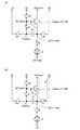
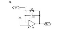
〈発光装置の構成例〉
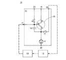
図1に、本発明の一態様にかかる発光装置の構成を、一例として示す。図1に示す発光装
置10は、画素11と、モニター回路12と、画像処理回路13とを有する。画素11は
、発光素子14、トランジスタ15、スイッチ16、スイッチ17、及び容量素子18を
少なくとも有する。<Example of configuration of light emitting device>
FIG. 1 shows a structure of a light emitting device according to one embodiment of the present invention as an example. The
発光素子14は、LED(Light Emitting Diode)やOLED(O
rganic Light Emitting Diode)などの、電流または電圧に
よって輝度が制御される素子をその範疇に含んでいる。例えば、OLEDは、EL層と、
陽極と、陰極とを少なくとも有している。EL層は陽極と陰極の間に設けられた単層また
は複数の層で構成されており、これらの層の中に、発光性の物質を含む発光層を少なくと
も含んでいる。EL層は、陰極と陽極間の電位差が、発光素子14の閾値電圧以上になっ
たときに供給される電流により、エレクトロルミネッセンスが得られる。エレクトロルミ
ネッセンスには、一重項励起状態から基底状態に戻る際の発光(蛍光)と三重項励起状態
から基底状態に戻る際の発光(リン光)とが含まれる。The
The category includes an element whose luminance is controlled by current or voltage, such as an organic light emitting diode). For example, an OLED has an EL layer,
It has at least an anode and a cathode. The EL layer is composed of a single layer or a plurality of layers provided between an anode and a cathode, and at least a light emitting layer containing a light emitting substance is included in these layers. The EL layer can obtain electroluminescence by the current supplied when the potential difference between the cathode and the anode becomes equal to or higher than the threshold voltage of the
トランジスタ15は、配線21を介して画素11に入力された画像信号に従って、発光素
子14への電流の供給を制御する機能を有する。なお、トランジスタ15は、通常のゲー
ト(第1ゲート)に加えて、閾値電圧を制御するためのバックゲート(第2ゲート)を有
していても良い。The
なお、図1では、トランジスタ15がnチャネル型である場合を例示しているが、この場
合、トランジスタ15のソースは、発光素子14の陽極に接続されている。そして、トラ
ンジスタ15のドレインは配線19に接続されており、発光素子14の陰極は、配線20
に接続されている。また、配線19の電位は、配線20の電位に発光素子14の閾値電圧
Vtheと、トランジスタ15の閾値電圧Vthとを加算した電位よりも、高いものとす
る。よって、画素11に入力される画像信号に従い、トランジスタ15のドレイン電流の
値が定まると、上記ドレイン電流が発光素子14に供給されることで、発光素子14は発
光の状態となる。そして、発光素子14の輝度は、ドレイン電流の値によって定まる。Note that FIG. 1 illustrates the case where the
It is connected to the. The potential of the
トランジスタ15がpチャネル型である場合は、トランジスタ15のソースは、発光素子
14のカソードに接続される。そして、トランジスタ15のドレインは配線19に接続さ
れており、発光素子14のアノードは、配線20に接続される。また、配線20の電位は
、配線19の電位に発光素子14の閾値電圧Vtheと、トランジスタ15の閾値電圧V
thとを加算した電位よりも、高いものとする。そして、トランジスタ15がnチャネル
型である場合と同様に、トランジスタ15がpチャネル型である場合も、画素11に入力
される画像信号に従い、トランジスタ15のドレイン電流の値が定まると、上記ドレイン
電流が発光素子14に供給されることで、発光素子14は発光の状態となる。そして、発
光素子14の輝度は、ドレイン電流の値によって定まる。When the
It should be higher than the potential obtained by adding th. Similarly to the case where the
また、スイッチ16は、トランジスタ15のゲート(Gで示す)と、配線23の間の導通
状態を制御する機能を有する。例えば、スイッチ16は、トランジスタを単数または複数
用いて構成することができる。或いは、スイッチ16は、単数または複数のトランジスタ
に加えて、容量素子を用いていても良い。スイッチ17は、トランジスタ15に流れるド
レイン電流の、上記画素11からの取り出しを制御する機能を有する。スイッチ17は、
トランジスタを単数または複数用いて構成することができる。具体的に、スイッチ17は
、配線22と、トランジスタ15のソースとの間の導通状態を制御する。The
A single transistor or a plurality of transistors can be used. Specifically, the
配線23は配線19と電気的に接続されていても良い。この場合、スイッチ16は、トラ
ンジスタ15のゲートとドレイン(Dで示す)の間の導通状態を制御する機能を有する。
或いは、配線23は配線19と、電気的に分離されていても良い。いずれの場合において
も、トランジスタ15がnチャネル型である場合、配線23の電位は、配線20の電位に
発光素子14の閾値電圧Vtheと、トランジスタ15の閾値電圧Vthとを加算した電
位よりも、高いものとする。また、トランジスタ15がpチャネル型である場合、配線2
3の電位は、配線20の電位から、発光素子14の閾値電圧Vtheと、トランジスタ1
5の閾値電圧Vthとを差し引いた電位よりも、低いものとする。The
Alternatively, the
The potential of 3 is based on the potential of the
It is lower than the potential obtained by subtracting the threshold voltage Vth of 5.
容量素子18は、トランジスタ15のゲートとソース(Sで示す)の電位差、すなわち、
ゲート電圧Vgsを保持する機能を有する。ただし、容量素子18は、例えばトランジス
タ15のゲートと半導体膜の間に形成されるゲート容量が十分大きい場合などは、必ずし
も画素11に設ける必要はない。The
It has a function of holding the gate voltage Vgs. However, the
本発明の一態様では、画素11において、画像信号に従ってトランジスタ15のドレイン
電流の値を定める前に、上記スイッチ16によりトランジスタ15のゲートと配線23を
導通させた状態において、トランジスタ15の閾値電圧を取得する。或いは、上記スイッ
チ16によりトランジスタ15のゲートとドレインを導通させた状態において、トランジ
スタ15の閾値電圧を取得する。閾値電圧を取得して、画像信号に従ってトランジスタ1
5のドレイン電流の値を定めることで、画素11間において生じた閾値電圧のばらつきが
、上記ドレイン電流の値に影響を及ぼすのを防ぐことができる。According to one embodiment of the present invention, in the
By setting the value of the drain current of 5, it is possible to prevent the variation of the threshold voltage generated between the
例えば、トランジスタ15がnチャネル型である場合、閾値電圧を取得する前の段階にお
いて、配線23の電位をトランジスタ15のソースの電位よりも高く保つ。具体的には、
トランジスタ15のソースの電位に、トランジスタ15の閾値電圧Vthを加算した電位
よりも高くなるように、トランジスタ15のソースと配線23との間に電位差Vonを設
ける。トランジスタ15のゲート電圧Vgsは、電位差Vonと等しくなるため、トラン
ジスタ15はオンになり、ドレイン電流が流れる。For example, in the case where the
A potential difference Von is provided between the source of the
次いで、トランジスタ15のソースをフローティングの状態にし、トランジスタ15のド
レイン電流が容量素子18にのみ流れる構成とする。上記構成により、容量素子18に蓄
積されている電荷が放出され、トランジスタ15のソースの電位が上昇する。トランジス
タ15のゲート電圧Vgsは、ドレイン電流が流れ始めた当初は電位差Vonと等しい値
を有しているが、ソースの電位の上昇に伴い、徐々に小さくなっていく。そして、トラン
ジスタ15のゲート電圧Vgsが閾値電圧Vthに近づくと、ドレイン電流が0Aに収束
する。その結果、容量素子18に閾値電圧Vthが保持され、閾値電圧Vthの取得が完
了する。Then, the source of the
上記一連の動作により、画素11間に存在するトランジスタ15の閾値電圧のばらつきを
補正することができ、画素11間における発光素子14の輝度のばらつきを抑えることが
できる。Through the series of operations described above, variation in the threshold voltage of the
なお、上述したように、本発明の一態様では、画素11が、スイッチ16によりトランジ
スタ15のゲートと配線23間の導通状態が制御できる構成を有していれば良い。また、
本発明の一態様では、画素11が、容量素子18に、或いは容量素子18がない場合はト
ランジスタ15のゲート容量に、トランジスタ15のゲート電圧Vgsを保持できる構成
であれば良い。そして、トランジスタ15に流れるドレイン電流により容量素子18に蓄
積された電荷が放出され、その結果、トランジスタ15の閾値電圧が容量素子18に保持
される構成であれば良い。また、本発明の一態様では、画素11が、トランジスタ15に
流れるドレイン電流の、画素11からの取り出しを、スイッチ17により制御できる構成
を有していれば良い。よって、画素11は、トランジスタ15、スイッチ16、スイッチ
17、容量素子18のみならず、トランジスタ、容量素子、抵抗、インダクタなどの他の
回路素子をさらに有していても良い。そして、上記構成を満たすように、他の回路素子が
、トランジスタ15、スイッチ16、スイッチ17、容量素子18、配線19間に設けら
れていても良い。Note that as described above, in one embodiment of the present invention, the
In one embodiment of the present invention, the
また、モニター回路12は、スイッチ17を介して画素11から取り出された、トランジ
スタ15のドレイン電流を用いて、当該電流の値を情報として含む信号を、生成する機能
を有する。モニター回路12として、例えば、積分回路などの、電流電圧変換回路を用い
ることができる。トランジスタ15のドレイン電流には、トランジスタ15の移動度や、
トランジスタ15のサイズ(チャネル幅やチャネル長)に関連した情報が含まれている。Further, the
Information about the size of the transistor 15 (channel width or channel length) is included.
画像処理回路13は、モニター回路12で生成された上記信号に従って、画素11に入力
される画像信号を補正する機能を有する。具体的には、モニター回路12で生成された信
号から、トランジスタ15のドレイン電流が所望の値よりも大きかったと判断された場合
、トランジスタ15のドレイン電流が小さくなるように、画像信号を補正する。逆に、モ
ニター回路12で生成された信号から、トランジスタ15のドレイン電流が所望の値より
も小さかったと判断された場合、トランジスタ15のドレイン電流が大きくなるように、
画像信号を補正する。The
Correct the image signal.
画像信号の補正により、画素11間に存在するトランジスタ15の閾値電圧のばらつきの
みならず、トランジスタ15の移動度などのその他の電気的特性のばらつきをも、補正す
ることができる。よって、画素11内において、閾値電圧の補正を行う場合よりも、画素
11間における発光素子14の輝度のばらつきを、さらに抑えることができる。By the correction of the image signal, not only the variation of the threshold voltage of the
なお、画素11内における閾値電圧の補正(以下、内部補正と呼ぶ)を行わずに、画像処
理回路13における画像信号の補正(以下、外部補正と呼ぶ)を行う場合でも、画素11
間に存在するトランジスタ15の閾値電圧のばらつきのみならず、トランジスタ15の移
動度などのその他の電気的特性のばらつきをも、補正することができる。しかし、内部補
正を行わず、外部補正だけ行う場合、内部補正も外部補正も行わない補正なしの場合に比
べると、画像信号の電位の振幅を大きく取る必要がある。Even when the correction of the threshold voltage in the pixel 11 (hereinafter, referred to as internal correction) is not performed and the image signal is corrected in the image processing circuit 13 (hereinafter, referred to as external correction), the
It is possible to correct not only the variation in the threshold voltage of the
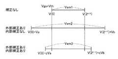
図3に、補正なしの場合の、画像信号の電位の振幅Vam1と、外部補正ありで内部補正
なしの場合の、画像信号の電位の振幅Vam2とを、図3に模式的に示す。なお、総階調
数は2nであると仮定する。FIG. 3 schematically shows the
図3に示すように、補正なしの場合の、振幅Vam1は、最小の階調値0に対応する画像
信号の電位V(0)と、最大の階調値2n−1に対応する画像信号の電位V(2n−1)
との電位差に相当する。また、図3に示すように、外部補正ありで内部補正なしの場合、
最小の階調値0に対応する画像信号は、トランジスタ15における閾値電圧のマイナスシ
フトや移動度のプラスシフトを考慮した場合、電位V(0)−Vaとなる。そして、最大
の階調値2n−1に対応する画像信号は、トランジスタ15における閾値電圧のプラスシ
フトや移動度のマイナスシフトを考慮した場合、電位V(2n−1)+Vbとなる。よっ
て、振幅Vam2は、電位V(0)−Vaと、電位V(2n−1)+Vbの電位差に相当
する。As shown in FIG. 3, the
Corresponds to the potential difference between and. In addition, as shown in FIG. 3, when external correction is performed and internal correction is not performed,
The image signal corresponding to the
したがって、外部補正ありで内部補正なしの場合の、画像信号の電位の振幅Vam2は、
補正なしの場合の、画像信号の電位の振幅Vam1に比べて、大きくなる。そして、振幅
Vam2が大きすぎると、階調値間における画像信号の電位差も大きくなるため、外部補
正ありで内部補正なしの場合、画像内の輝度の変化をなめらかなグラデーションで表現す
ることが難しく、画質が低下しやすい。総階調数を増やし、階調値間における画像信号の
電位差を小さくすることで、画質の低下を防ぐことはできる。しかし、この場合、デジタ
ルの画像信号を扱う、画像処理回路13、コントローラ、画像メモリなどにおいて、画像
信号の転送や、その他の信号処理に要する時間や電力が増大する。そのため、画像処理回
路13、コントローラ、画像メモリの高速動作と低消費電力を考慮すると、nビットの総
階調数を、せいぜい2ビット分しか増加させることができず、振幅Vam2が大きい場合
は画質の低下を防ぐことが難しい。Therefore, the amplitude Vam 2 of the potential of the image signal with external correction and without internal correction is
The amplitude becomes larger than the
本発明の一態様では、外部補正だけではなく内部補正をも行う。この場合の、画像信号の
電位の振幅Vam3を、図3に模式的に示す。外部補正ありで内部補正ありの場合、閾値
電圧のマイナスシフト或いはプラスシフトの補正は、内部補正によって行われる。よって
、外部補正では、移動度などの、トランジスタ15における閾値電圧以外の電気的特性の
ばらつきを補正すればよい。具体的に、図3に示すように、最小の階調値0に対応する画
像信号は、トランジスタ15における移動度のプラスシフトを考慮した場合、電位V(0
)−cVaとなる。cは、閾値電圧の内部補正により定まる定数であり、0.1乃至0.
3程度の、1以下の正の数となる。そして、最大の階調値2n−1に対応する画像信号は
、トランジスタ15における移動度のマイナスシフトを考慮した場合、電位V(2n−1
)+cVbとなる。よって、振幅Vam3は、電位V(0)−cVaと、電位V(2n−
1)+cVbの電位差に相当し、当該電位差は、振幅Vam1よりも大きくなるが、振幅
Vam2よりも小さくなる。In one embodiment of the present invention, not only external correction but also internal correction is performed. The
)-CVa. c is a constant determined by the internal correction of the threshold voltage, and is 0.1 to 0.
It is a positive number of 1 or less, which is about 3. Then, the image signal corresponding to the maximum gradation value 2n−1 has a potential V(2n−1 ) when the negative shift of the mobility of the
)+cVb. Therefore, the
1 )+cVb, which is larger than the
したがって、本発明の一態様では、外部補正と内部補正を組み合わせることで、内部補正
を行わず外部補正だけ行う場合に比べて、画像信号の電位の振幅を小さく抑えることがで
きる。よって、トランジスタ15の電気的特性のばらつきに起因する、画像の輝度むらを
補正することができ、なおかつ、階調値間における画像信号の電位差を小さく抑え、画質
の低下を防ぐことができる。そして、本発明の一態様では、外部補正と内部補正を組み合
わせることで、内部補正だけでは対応しきれなかった、移動度などの、閾値電圧以外の電
気的特性の補正も、行うことができる。Therefore, in one embodiment of the present invention, by combining external correction and internal correction, the amplitude of the potential of the image signal can be suppressed smaller than in the case where only internal correction is performed and only external correction is performed. Therefore, it is possible to correct the unevenness in the brightness of the image due to the variation in the electrical characteristics of the
なお、外部補正は、必ずしも、画像を書き換えるごとに行わなくてもよい。例えば、所定
の期間においてのみ、外部補正を行ってもよい。The external correction does not necessarily have to be performed each time the image is rewritten. For example, the external correction may be performed only in a predetermined period.
ただし、本発明の一態様は、外部補正と内部補正の両方を行う期間があってもよいし、外
部補正と内部補正の何れか一つのみを行う期間があってもよいし、両方を行わない期間が
あってもよい。However, according to one embodiment of the present invention, there may be a period in which both external correction and internal correction are performed, a period in which only one of external correction and internal correction is performed, or both are performed. There may be no period.
〈発光装置の具体的な構成例〉
次いで、図1に示した発光装置10の、より詳細な構成の一例について説明する。図2に
、本発明の一態様に係る発光装置10の構成を、ブロック図で一例として示す。なお、ブ
ロック図では、構成要素を機能ごとに分類し、互いに独立したブロックとして示している
が、実際の構成要素は機能ごとに完全に切り分けることが難しく、一つの構成要素が複数
の機能に係わることもあり得る。<Specific configuration example of light emitting device>
Next, an example of a more detailed configuration of the
図2に示す発光装置10は、画素11を画素部24に複数有するパネル25と、コントロ
ーラ26と、CPU27と、画像処理回路13と、画像メモリ28と、メモリ29と、モ
ニター回路12とを有する。また、図2に示す発光装置10は、パネル25に、駆動回路
30と、駆動回路31とを有する。The
CPU27は、外部から入力された命令、またはCPU27内に設けられたメモリに記憶
されている命令をデコードし、発光装置10が有する各種回路の動作を統括的に制御する
ことで、当該命令を実行する機能を有する。The
モニター回路12は、画素11から出力されたドレイン電流から、上記ドレイン電流の値
を情報として含む信号を生成する。メモリ29は、当該信号に含まれる上記情報を記憶す
る機能を有する。なお、メモリ29は、DRAMやSRAMのような揮発性のメモリを用
いてもよいし、フラッシュメモリ、MRAM、磁気メモリ、磁気ディスク、光磁気ディス
クなどのような不揮発性のメモリを用いてもよい。例えば、メモリ29として、不揮発性
のメモリを用いることにより、電源の供給を停止した後でも、各画素の情報を記憶するこ
とが出来る。そのため、画素11からドレイン電流を出力する動作を、常に行わなくても
よいようにすることが出来る。例えば、製品を出荷する前や、電源の供給を停止する直前
や、電源の供給を開始した直後などにのみ、画素11からドレイン電流を出力する動作を
行い、その情報をメモリ29に保存しておくことが出来る。The
画像メモリ28は、発光装置10に入力された画像データ32を、記憶する機能を有する
。なお、図2では、画像メモリ28を1つだけ発光装置10に設ける場合を例示している
が、複数の画像メモリ28が発光装置10に設けられていても良い。例えば、赤、青、緑
などの色相にそれぞれ対応する3つの画像データ32により、画素部24にフルカラーの
画像が表示される場合、各画像データ32に対応した画像メモリ28を、それぞれ設ける
ようにしても良い。The
画像メモリ28には、例えばDRAM(Dynamic Random Access
Memory)、SRAM(Static Random Access Memory
)等の記憶回路を用いることができる。或いは、画像メモリ28に、VRAM(Vide
o RAM)を用いても良い。The
Memory), SRAM (Static Random Access Memory)
) Or the like can be used. Alternatively, the
o RAM) may be used.
画像処理回路13は、CPU27からの命令に従い、画像データ32の画像メモリ28へ
の書き込みと、画像データ32の画像メモリ28からの読み出しを行い、画像データ32
から画像信号Sigを生成する機能を有する。また、画像処理回路13は、CPU27か
らの命令に従い、メモリ29に記憶されている情報を読み出し、当該情報を用いて、画像
信号の補正を行う機能を有する。The
From the image signal Sig. Further, the
コントローラ26は、画像情報を有する画像信号Sigが入力されると、パネル25の仕
様に合わせて画像信号Sigに信号処理を施した後、パネル25に供給する機能を有する
。When the image signal Sig having the image information is input, the controller 26 has a function of performing signal processing on the image signal Sig according to the specifications of the panel 25 and then supplying the image signal Sig to the panel 25.
駆動回路31は、画素部24が有する複数の画素11を、行ごとに選択する機能を有する
。また、駆動回路30は、コントローラ26から与えられた画像信号Sigを、駆動回路
31によって選択された行の画素11に供給する機能を有する。The
なお、コントローラ26は、駆動回路30や駆動回路31などの駆動に用いられる各種の
駆動信号を、パネル25に供給する機能を有する。駆動信号には、駆動回路30の動作を
制御するスタートパルス信号SSP、クロック信号SCK、ラッチ信号LP、駆動回路3
1の動作を制御するスタートパルス信号GSP、クロック信号GCKなどが含まれる。The controller 26 has a function of supplying various drive signals used for driving the drive circuit 30 and the
The start pulse signal GSP and the clock signal GCK for controlling the operation No. 1 are included.
なお、発光装置10は、発光装置10が有するCPU27に、情報や命令を与える機能を
有する入力装置を、有していても良い。入力装置として、キーボード、ポインティングデ
バイス、タッチパネル、センサなどを用いることができる。The
〈画素の構成例1〉
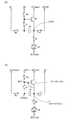
次いで、図1に示す発光装置10が有する、画素11の具体的な構成例について説明する
。<Pixel configuration example 1>
Next, a specific configuration example of the
図4に、画素11の回路図の一例を示す。画素11は、トランジスタ15と、スイッチ1
6として機能するトランジスタ16tと、スイッチ17として機能するトランジスタ17
tと、容量素子18と、発光素子14と、トランジスタ40乃至トランジスタ42とを有
する。FIG. 4 shows an example of a circuit diagram of the
t, the
発光素子14の画素電極は、画素11に入力される画像信号Sigに従ってその電位が制
御される。また、発光素子14の輝度は、画素電極と共通電極の間の電位差によって定ま
る。例えば、OLEDを発光素子14として用いる場合、陽極と陰極のいずれか一方が画
素電極として機能し、他方が共通電極として機能する。図4では、発光素子14の陽極を
画素電極として用い、発光素子14の陰極を共通電極として用いた画素11の構成を例示
している。The potential of the pixel electrode of the
トランジスタ40は、配線21と、容量素子18の一対の電極のうちの一方との間の導通
状態を制御する機能を有する。容量素子18の一対の電極のうちの他方は、トランジスタ
15のソース及びドレインの一方に接続される。トランジスタ16tは、配線23と、ト
ランジスタ15のゲートとの間の導通状態を制御する機能を有する。トランジスタ41は
、容量素子18の一対の電極のうちの一方と、トランジスタ15のゲートとの間の導通状
態を制御する機能を有する。トランジスタ42は、トランジスタ15のソース及びドレイ
ンの一方と、発光素子14の陽極との間の導通状態を制御する機能を有する。トランジス
タ17tは、トランジスタ15のソース及びドレインの一方と、配線22との間の導通状
態を制御する機能を有する。The
さらに、図4では、トランジスタ15のソース及びドレインの他方は配線19に接続され
ている。Further, in FIG. 4, the other of the source and the drain of the
また、トランジスタ40におけるオンまたはオフの選択は、トランジスタ40のゲートに
接続された配線43の電位に従って行われる。トランジスタ16tにおけるオンまたはオ
フの選択は、トランジスタ16tのゲートに接続された配線43の電位に従って行われる
。トランジスタ41におけるオンまたはオフの選択は、トランジスタ41のゲートに接続
された配線44の電位に従って行われる。トランジスタ42におけるオンまたはオフの選
択は、トランジスタ42のゲートに接続された配線44の電位に従って行われる。トラン
ジスタ17tにおけるオンまたはオフの選択は、トランジスタ17tのゲートに接続され
た配線45の電位に従って行われる。Further, the selection of ON or OFF in the
画素11が有するトランジスタには、酸化物半導体や、非晶質、微結晶、多結晶、又は単
結晶の、シリコン、又はゲルマニウムなどの半導体を用いることができる。トランジスタ
40、トランジスタ16t及びトランジスタ41が酸化物半導体をチャネル形成領域に含
むことで、トランジスタ40、トランジスタ16t及びトランジスタ41のオフ電流を極
めて小さくすることができる。そして、上記構成を有するトランジスタ40、トランジス
タ16t及びトランジスタ41を画素11に用いることで、通常のシリコンやゲルマニウ
ムなどの半導体で形成されたトランジスタをトランジスタ40、トランジスタ16t及び
トランジスタ41に用いる場合に比べて、トランジスタ15のゲートに蓄積された電荷の
リークを防ぐことができる。For the transistor included in the
よって、静止画のように、連続する幾つかのフレーム期間に渡って、画素部に同じ画像情
報を有する画像信号Sigが書き込まれる場合などは、駆動周波数を低くする、言い換え
ると一定期間内における画素部への画像信号Sigの書き込み回数を少なくしても、画像
の表示を維持することができる。例えば、高純度化された酸化物半導体をトランジスタ4
0、トランジスタ16t及びトランジスタ41の半導体膜に用いることで、画像信号Si
gの書き込みの間隔を10秒以上、好ましくは30秒以上、さらに好ましくは1分以上に
することができる。そして、画像信号Sigが書き込まれる間隔を長くすればするほど、
消費電力をより低減することができる。Therefore, when the image signal Sig having the same image information is written in the pixel portion over several continuous frame periods such as a still image, the driving frequency is lowered, in other words, the pixel within a certain period is reduced. Even if the number of times of writing the image signal Sig to the unit is reduced, the display of the image can be maintained. For example, a highly purified oxide semiconductor is used as the transistor 4
0, the
The writing interval of g can be 10 seconds or longer, preferably 30 seconds or longer, more preferably 1 minute or longer. Then, the longer the interval at which the image signal Sig is written, the more
The power consumption can be further reduced.
また、画像信号Sigの電位をより長い期間に渡って保持することができるため、トラン
ジスタ15のゲートの電位を保持するための容量素子18を画素11に設けなくとも、表
示される画質が低下するのを防ぐことができる。よって、容量素子18を設けないことに
よって、或いは容量素子18のサイズを小さくすることによって、画素11の開口率を高
めることができるため、発光素子14の長寿命化を実現し、延いては、発光装置10の信
頼性を高めることができる。Further, since the potential of the image signal Sig can be held for a longer period, the displayed image quality is deteriorated without providing the
なお、図4において、画素11は、必要に応じて、トランジスタ、ダイオード、抵抗素子
、容量素子、インダクタなどのその他の回路素子を、さらに有していても良い。Note that, in FIG. 4, the
また、図4において、各トランジスタは、ゲートを半導体膜の片側において少なくとも有
していれば良いが、半導体膜を間に挟んで存在する一対のゲートを有していても良い。一
対のゲートの一方をバックゲートとすると、通常のゲート及びバックゲートに同じ高さの
電位が与えられていても良いし、バックゲートにのみ接地電位などの固定の電位が与えら
れていても良い。バックゲートに与える電位の高さを制御することで、トランジスタの閾
値電圧を制御することができる。また、バックゲートを設けることで、チャネル形成領域
が増え、ドレイン電流の増加を実現することができる。また、バックゲートを設けること
で、半導体膜に空乏層ができやすくなるため、S値の改善を図ることができる。Further, in FIG. 4, each transistor needs to have at least a gate on one side of the semiconductor film, but may have a pair of gates which sandwich the semiconductor film therebetween. When one of the pair of gates is a back gate, the normal gate and the back gate may be given the same potential, or only the back gate may be given a fixed potential such as a ground potential. .. By controlling the height of the potential applied to the back gate, the threshold voltage of the transistor can be controlled. Further, by providing the back gate, the channel formation region can be increased and the drain current can be increased. In addition, since the depletion layer is easily formed in the semiconductor film by providing the back gate, the S value can be improved.
また、図4では、トランジスタが全てnチャネル型である場合を例示している。画素11
内のトランジスタが全て同じチャネル型である場合、トランジスタの作製工程において、
半導体膜に一導電性を付与する不純物元素の添加などの工程を、一部省略することができ
る。ただし、本発明の一態様に係る発光装置では、必ずしも画素11内のトランジスタが
全てnチャネル型である必要はない。発光素子14の陰極が配線20に接続されている場
合、少なくともトランジスタ15はnチャネル型であることが望ましく、発光素子14の
陽極が配線20に接続されている場合、少なくともトランジスタ15はpチャネル型であ
ることが望ましい。Further, FIG. 4 illustrates the case where all the transistors are n-channel type.
If all the transistors inside are the same channel type,
Steps such as addition of an impurity element imparting one conductivity type to the semiconductor film can be partially omitted. However, in the light-emitting device according to one embodiment of the present invention, all the transistors in the
また、図4では、画素11内のトランジスタが、単数のゲートを有することで、単数のチ
ャネル形成領域を有するシングルゲート構造である場合を例示しているが、本発明の一態
様はこの構成に限定されない。画素11内のトランジスタのいずれかまたは全てが、電気
的に接続された複数のゲートを有することで、複数のチャネル形成領域を有する、マルチ
ゲート構造であっても良い。Although FIG. 4 illustrates the case where the transistor in the
図5に、図4に示す画素11に接続される配線43、配線44、配線45の電位と、配線
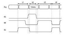
21に供給される画像信号Sigの電位のタイミングチャートを例示する。なお、図5に
示すタイミングチャートは、図4に示す画素11に含まれるトランジスタが全てnチャネ
ル型である場合を例示するものである。また、図6及び図7に、各期間における、画素1
1の動作を模式的に示す。ただし、図6及び図7では、画素11の動作を分かりやすく示
すために、トランジスタ15以外のトランジスタを、スイッチとして図示する。FIG. 5 illustrates a timing chart of the potentials of the
The operation of No. 1 is schematically shown. However, in FIGS. 6 and 7, transistors other than the
まず、期間t1では、配線43にローレベルの電位が与えられ、配線44にハイレベルの
電位が与えられ、配線45にハイレベルの電位が与えられる。よって、図6(A)に示す
ように、トランジスタ41、トランジスタ42、トランジスタ17tがオンとなり、トラ
ンジスタ40、トランジスタ16tはオフとなる。トランジスタ42およびトランジスタ
17tがオンになることで、トランジスタ15のソース及びドレインの一方および容量素
子18の一対の電極のうちの他方(ノードAとして図示する)に、配線22の電位V0が
与えられる。First, in the period t1, the
また、配線19には電位Vanoが与えられ、配線20には電位Vcatが与えられる。
電位Vanoは、電位V0に発光素子14の閾値電圧Vtheを加算した電位よりも高く
することが望ましい。また、電位V0は、電位Vcatに発光素子14の閾値電圧Vth
eを加算した電位よりも、低いことが望ましい。電位V0を上記値に設定することで、期
間t1において発光素子14に電流が流れるのを防ぐことができる。The potential Vano is applied to the
The potential Vano is preferably higher than the potential obtained by adding the threshold voltage Vthe of the
It is preferably lower than the potential obtained by adding e. By setting the potential V0 to the above value, current can be prevented from flowing to the
次いで、配線44にローレベルの電位が与えられることで、トランジスタ41及びトラン
ジスタ42がオフになり、ノードAは電位V0に保持される。Next, a low-level potential is applied to the
次いで、期間t2では、配線43にハイレベルの電位が与えられ、配線44にローレベル
の電位が与えられ、配線45にローレベルの電位が与えられる。よって、図6(B)に示
すように、トランジスタ40およびトランジスタ16tがオンとなり、トランジスタ41
、トランジスタ42及びトランジスタ17tがオフとなる。Next, in the period t2, the
, The
なお、期間t1から期間t2に移行する際、配線43に与える電位をローレベルからハイ
レベルに切り替えた後に、配線45に与える電位をハイレベルからローレベルに切り替え
ることが望ましい。このような動作を行うことによって、配線43に与えられる電位の切
り替えによる、ノードAの電位の変動を防ぐことができる。Note that when transitioning from the period t1 to the period t2, it is preferable that the potential applied to the
また、配線19には電位Vanoが与えられ、配線20には電位Vcatが与えられる。
そして、配線21には画像信号Sigの電位Vdataが与えられ、配線23には電位V
1が与えられる。電位V1は、電位Vcatにトランジスタ15の閾値電圧Vthを加算
した電位よりも高く、電位Vanoにトランジスタ15の閾値電圧Vthを加算した電位
より低いことが望ましい。The potential Vano is applied to the
The potential Vdata of the image signal Sig is applied to the
1 is given. The potential V1 is preferably higher than a potential obtained by adding the threshold voltage Vth of the
なお、図4に示す画素構成では、電位V1を、発光素子14の閾値電圧Vtheを電位V
catに加算した値より高くしても、トランジスタ42がオフである限り、発光素子14
は発光しない。そのため、電位V0として設定できる値の幅を広げることが可能となり、
V1−V0として取りうる値の幅も広げることが可能となる。したがって、V1−V0の
値の設定の自由度が上がるため、トランジスタ15の閾値電圧の取得に要する時間を短縮
した場合、または閾値電圧の取得期間に制限がある場合においても、正確にトランジスタ
15の閾値電圧の取得を行うことができる。Note that in the pixel configuration shown in FIG. 4, the potential V1 is the threshold voltage Vthe of the
Even if it is higher than the value added to cat, as long as the
Does not emit light. Therefore, it is possible to widen the range of values that can be set as the potential V0,
It is possible to widen the range of values that can be taken as V1-V0. Therefore, since the degree of freedom in setting the values of V1 to V0 is increased, even if the time required to acquire the threshold voltage of the
上記動作により、トランジスタ15のゲート(ノードBとして図示する)に、ノードAの
電位に閾値電圧を加算した電位よりも、高い電位V1が入力され、トランジスタ15がオ
ンとなる。よって、トランジスタ15を介して容量素子18の電荷が放出され、電位V0
だったノードAの電位が上昇を始める。そして、最終的にはノードAの電位がV1−Vt
hに収束し、トランジスタ15のゲート電圧が閾値電圧Vthに収束すると、トランジス
タ15がオフになる。Through the above operation, the potential V1 higher than the potential obtained by adding the threshold voltage to the potential of the node A is input to the gate of the transistor 15 (illustrated as the node B), so that the
Only the potential of the node A starts rising. And finally, the potential of the node A is V1-Vt.
When it converges to h and the gate voltage of the
また、容量素子18の一対の電極のうちの一方(ノードCとして図示する)には、配線2
1に与えられた画像信号Sigの電位Vdataが、トランジスタ40を介して与えられ
る。The wiring 2 is connected to one of the pair of electrodes of the capacitor 18 (illustrated as a node C).
The potential Vdata of the image signal Sig given to 1 is given via the
次いで、期間t3では、配線43にローレベルの電位が与えられ、配線44にハイレベル
の電位が与えられ、配線45にローレベルの電位が与えられる。よって、図7(A)に示
すように、トランジスタ41及びトランジスタ42がオンとなり、トランジスタ40、ト
ランジスタ16t及びトランジスタ17tがオフとなる。Next, in a period t3, the
なお、期間t2から期間t3に移行する際、配線43に与える電位がハイレベルからロー
レベルに切り替えられてから、配線44に与える電位をローレベルからハイレベルに切り
替えることが望ましい。上記構成により、配線43に与える電位の切り替えによるノード
Aにおける電位の変動を防ぐことができる。Note that when transitioning from the period t2 to the period t3, it is preferable that the potential applied to the
また、配線19には電位Vanoが与えられ、配線20には電位Vcatが与えられる。The potential Vano is applied to the
上記動作により、ノードBに電位Vdataが与えられるため、トランジスタ15のゲー
ト電圧がVdata−V1+Vthとなる。よって、トランジスタ15のゲート電圧を、
閾値電圧Vthが加味された値に設定することができる。上記構成により、トランジスタ
15の閾値電圧Vthのばらつきを抑制することができる。よって、発光素子14に供給
する電流値のばらつきを抑えることができ、発光装置の輝度ムラを低減することができる
。By the above operation, the potential Vdata is applied to the node B, so that the gate voltage of the
The threshold voltage Vth can be set to a value with consideration. With the above structure, variation in the threshold voltage Vth of the
なお、配線44に与える電位の変動を大きくしておくことで、トランジスタ42の閾値電
圧のばらつきが発光素子14に供給する電流値に影響を及ぼすことを防ぐことができる。
つまり、配線44に与えるハイレベルの電位をトランジスタ42の閾値電圧よりも十分大
きく、また、配線44に与えるローレベルの電位をトランジスタ42の閾値電圧よりも十
分小さくしてやることで、トランジスタ42のオンとオフの切り替えを確実に行い、トラ
ンジスタ42の閾値電圧のばらつきが発光素子14の電流値に影響を及ぼすことを防ぐこ
とができる。Note that by increasing the fluctuation of the potential applied to the
That is, the high-level potential applied to the
次いで、期間t4では、配線43にローレベルの電位が与えられ、配線44にローレベル
の電位が与えられ、配線45にハイレベルの電位が与えられる。よって、図7(B)に示
すように、トランジスタ17tがオンとなり、トランジスタ16t、トランジスタ40、
トランジスタ41及びトランジスタ42がオフとなる。Next, in the period t4, the
The
また、配線19には電位Vanoが与えられ、配線22は、モニター回路に接続される。The potential Vano is applied to the
上記動作により、トランジスタ15のドレイン電流Idが、発光素子14ではなく、トラ
ンジスタ17tを介して配線22に流れる。モニター回路は、配線22に流れたドレイン
電流Idを用いて、当該ドレイン電流Idの値を情報として含む信号を生成する。このド
レイン電流Idは、トランジスタ15の移動度やトランジスタ15のサイズ(チャネル長
、チャネル幅)などに依存した大きさとなっている。そして、本発明の一態様にかかる発
光装置では、上記信号を用いて、画素11に供給される画像信号Vsigの電位Vdat
aの値を、補正することができる。つまり、トランジスタ15の移動度のばらつきの影響
を低減することが出来る。By the above operation, the drain current Id of the
The value of a can be corrected. That is, the influence of variation in mobility of the
なお、図4に示す画素11を有する発光装置では、期間t3の動作の後に期間t4の動作
を常に行う必要はない。例えば、発光装置において、期間t1乃至期間t3の動作を複数
回繰り返した後に、期間t4の動作を行うようにしても良い。また、一行の画素11にお
いて期間t4の動作を行った後、最小の階調値0に対応する画像信号を、当該動作を行っ
た一行の画素11に書き込むことで、発光素子14を非発光の状態にした後、次の行の画
素11において、期間t4の動作を行うようにしても良い。Note that in the light-emitting device including the
図4に示した画素11を有する発光装置では、トランジスタ15のソース及びドレインの
他方と、トランジスタ15のゲートとが電気的に分離しているので、それぞれの電位を個
別に制御することができる。よって、期間t2において、トランジスタ15のソース及び
ドレインの他方の電位を、トランジスタ15のゲートの電位に、閾値電圧Vthを加算し
た電位よりも高い値に設定することができる。そのため、トランジスタ15がノーマリオ
ンである場合に、すなわち閾値電圧Vthがマイナスの値を有している場合に、トランジ
スタ15において、ソースの電位がゲートの電位V1よりも高くなるまで、容量素子18
に電荷を蓄積することができる。よって、本発明の一態様に係る発光装置では、トランジ
スタ15がノーマリオンであっても、期間t2において閾値電圧を取得することができ、
期間t3において、閾値電圧Vthを加味した値になるよう、トランジスタ15のゲート
電圧を設定することができる。In the light emitting device having the
Can store charge. Therefore, in the light-emitting device according to one embodiment of the present invention, the threshold voltage can be obtained in the period t2 even when the
In the period t3, the gate voltage of the
したがって、本発明の一態様に係る発光装置では、例えばトランジスタ15の半導体膜に
酸化物半導体を用いた場合などに、トランジスタ15がノーマリオンとなっても、表示ム
ラを低減でき、高い画質の表示を行うことができる。Therefore, in the light-emitting device according to one embodiment of the present invention, for example, when an oxide semiconductor is used for the semiconductor film of the
なお、トランジスタ15の特性だけでなく、発光素子14の特性もモニターしてもよい。
その場合の動作の例を、図20に示す。このとき、画像信号Sigの電位Vdataの電
位の制御することなどにより、トランジスタ15には、電流が流れないようにしておくこ
とが望ましい。これにより、発光素子14の電流を取り出すことが出来る。その結果、発
光素子14の電流特性の劣化やばらつきの状態を取得することが出来る。Note that not only the characteristics of the
An example of the operation in that case is shown in FIG. At this time, it is desirable to prevent a current from flowing through the
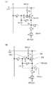
〈画素とモニター回路の接続構成〉
図4に示した画素11とモニター回路の、接続構成の一例について説明する。図19に、
図4に示した画素11と、選択回路64とを例示する。<Connection configuration of pixel and monitor circuit>
An example of the connection configuration of the
The
選択回路64は、電位V0が供給される配線67と、モニター回路に接続される端子TE
Rのいずれか一方を選択し、画素11の配線22と導通させる機能を有する。具体的に、
図19に示す選択回路64は、トランジスタ65とトランジスタ66を有する。トランジ
スタ65は、ゲートに接続された配線PRECの電位に従って、オンまたはオフが選択さ
れる。そして、トランジスタ65のソース及びドレインは、一方が配線67に接続されて
おり、他方が配線22に接続されている。トランジスタ66は、ゲートに接続された配線
SELの電位に従って、オンまたはオフが選択される。そして、トランジスタ66のソー
ス及びドレインは、一方が配線22に接続されており、他方が端子TERに接続されてい
る。The
It has a function of selecting one of R and connecting it to the
The
〈画素の構成例2〉
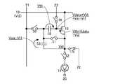
次いで、図1に示す発光装置10が有する画素11の、図4とは異なる具体的な構成例に
ついて説明する。<Pixel configuration example 2>
Next, a specific configuration example of the
図8に、画素11の回路図の一例を示す。画素11は、トランジスタ15と、スイッチ1
6として機能するトランジスタ16tと、スイッチ17として機能するトランジスタ17
tと、容量素子18と、発光素子14と、トランジスタ50乃至トランジスタ52と、容
量素子53と、を有する。FIG. 8 shows an example of a circuit diagram of the
t, the
発光素子14の画素電極は、画素11に入力される画像信号Sigに従ってその電位が制
御される。また、発光素子14の輝度は、画素電極と共通電極の間の電位差によって定ま
る。例えば、OLEDを発光素子14として用いる場合、陽極と陰極のいずれか一方が画
素電極として機能し、他方が共通電極として機能する。図8では、発光素子14の陽極を
画素電極として用い、発光素子14の陰極を共通電極として用いた画素11の構成を例示
している。The potential of the pixel electrode of the
トランジスタ50は、配線21と、容量素子18の一対の電極のうちの一方との間の導通
状態を制御する機能を有する。容量素子18の一対の電極のうちの他方は、トランジスタ
15のゲートに接続されている。トランジスタ16tは、配線23と、トランジスタ15
のゲートとの間の導通状態を制御する機能を有する。トランジスタ51は、容量素子18
の一対の電極のうちの一方と、トランジスタ15のソース及びドレインの一方との間の導
通状態を制御する機能を有する。トランジスタ52は、トランジスタ15のソース及びド
レインの一方と、発光素子14の陽極との間の導通状態を制御する機能を有する。トラン
ジスタ17tは、トランジスタ15のソース及びドレインの一方と、配線22との間の導
通状態を制御する機能を有する。さらに、図8では、トランジスタ15のソース及びドレ
インの他方は配線19に接続されている。容量素子53が有する一対の電極は、一方が、
容量素子18の一対の電極のうちの一方に接続され、他方が、トランジスタ15のソース
及びドレインの一方に接続されている。The
It has a function of controlling the conduction state between the gate and the gate. The
Has a function of controlling electrical continuity between one of the pair of electrodes and one of a source and a drain of the
The
また、トランジスタ50におけるオンまたはオフの選択は、トランジスタ50のゲートに
接続された配線56の電位に従って行われる。トランジスタ16tにおけるオンまたはオ
フの選択は、トランジスタ16tのゲートに接続された配線55の電位に従って行われる
。トランジスタ51におけるオンまたはオフの選択は、トランジスタ51のゲートに接続
された配線55の電位に従って行われる。トランジスタ52におけるオンまたはオフの選
択は、トランジスタ52のゲートに接続された配線57の電位に従って行われる。トラン
ジスタ17tにおけるオンまたはオフの選択は、トランジスタ17tのゲートに接続され
た配線54の電位に従って行われる。The selection of on or off of the
画素11が有するトランジスタには、酸化物半導体や、非晶質、微結晶、多結晶、又は単
結晶の、シリコン、又はゲルマニウムなどの半導体を用いることができる。トランジスタ
16tが酸化物半導体をチャネル形成領域に含むことで、トランジスタ16tのオフ電流
を極めて小さくすることができる。そして、上記構成を有するトランジスタ16tを画素
11に用いることで、通常のシリコンやゲルマニウムなどの半導体で形成されたトランジ
スタをトランジスタ16tに用いる場合に比べて、トランジスタ15のゲートに蓄積され
た電荷のリークを防ぐことができる。For the transistor included in the
よって、静止画のように、連続する幾つかのフレーム期間に渡って、画素部に同じ画像情
報を有する画像信号Sigが書き込まれる場合などは、駆動周波数を低くする、言い換え
ると一定期間内における画素部への画像信号Sigの書き込み回数を少なくしても、画像
の表示を維持することができる。例えば、高純度化された酸化物半導体をトランジスタ5
0の半導体膜に用いることで、画像信号Sigの書き込みの間隔を10秒以上、好ましく
は30秒以上、さらに好ましくは1分以上にすることができる。そして、画像信号Sig
が書き込まれる間隔を長くすればするほど、消費電力をより低減することができる。Therefore, when the image signal Sig having the same image information is written in the pixel portion over several continuous frame periods such as a still image, the driving frequency is lowered, in other words, the pixel within a certain period is reduced. Even if the number of times of writing the image signal Sig to the unit is reduced, the display of the image can be maintained. For example, a highly purified oxide semiconductor is used as the transistor 5
By using the semiconductor film of No. 0, the writing interval of the image signal Sig can be 10 seconds or longer, preferably 30 seconds or longer, and more preferably 1 minute or longer. Then, the image signal Sig
The longer the interval at which is written, the more power consumption can be reduced.
また、画像信号Sigの電位をより長い期間に渡って保持することができるため、トラン
ジスタ15のゲートの電位を保持するための容量素子18を画素11に設けなくとも、表
示される画質が低下するのを防ぐことができる。よって、容量素子18を設けないことに
よって、或いは容量素子18のサイズを小さくすることによって、画素11の開口率を高
めることができるため、発光素子14の長寿命化を実現し、延いては、発光装置10の信
頼性を高めることができる。Further, since the potential of the image signal Sig can be held for a longer period, the displayed image quality is deteriorated without providing the
なお、図8において、画素11は、必要に応じて、トランジスタ、ダイオード、抵抗素子
、容量素子、インダクタなどのその他の回路素子を、さらに有していても良い。Note that in FIG. 8, the
また、図8において、各トランジスタは、ゲートを半導体膜の片側において少なくとも有
していれば良いが、半導体膜を間に挟んで存在する一対のゲートを有していても良い。一
対のゲートの一方をバックゲートとすると、通常のゲート及びバックゲートに同じ高さの
電位が与えられていても良いし、バックゲートにのみ接地電位などの固定の電位が与えら
れていても良い。バックゲートに与える電位の高さを制御することで、トランジスタの閾
値電圧を制御することができる。また、バックゲートを設けることで、チャネル形成領域
が増え、ドレイン電流の増加を実現することができる。また、バックゲートを設けること
で、半導体膜に空乏層ができやすくなるため、S値の改善を図ることができる。Further, in FIG. 8, each transistor needs to have at least a gate on one side of the semiconductor film, but may have a pair of gates which sandwich the semiconductor film therebetween. When one of the pair of gates is a back gate, the normal gate and the back gate may be given the same potential, or only the back gate may be given a fixed potential such as a ground potential. .. By controlling the height of the potential applied to the back gate, the threshold voltage of the transistor can be controlled. Further, by providing the back gate, the channel formation region can be increased and the drain current can be increased. In addition, since the depletion layer is easily formed in the semiconductor film by providing the back gate, the S value can be improved.
また、図8では、トランジスタが全てnチャネル型である場合を例示している。画素11
内のトランジスタが全て同じチャネル型である場合、トランジスタの作製工程において、
半導体膜に一導電性を付与する不純物元素の添加などの工程を、一部省略することができ
る。ただし、本発明の一態様に係る発光装置では、必ずしも画素11内のトランジスタが
全てnチャネル型である必要はない。発光素子14の陰極が配線20に接続されている場
合、少なくともトランジスタ15はnチャネル型であることが望ましく、発光素子14の
陽極が配線20に接続されている場合、少なくともトランジスタ15はpチャネル型であ
ることが望ましい。Further, FIG. 8 illustrates the case where all the transistors are n-channel types.
If all the transistors inside are the same channel type,
Steps such as addition of an impurity element imparting one conductivity type to the semiconductor film can be partially omitted. However, in the light-emitting device according to one embodiment of the present invention, all the transistors in the
また、図8では、画素11内のトランジスタが、単数のゲートを有することで、単数のチ
ャネル形成領域を有するシングルゲート構造である場合を例示しているが、本発明はこの
構成に限定されない。画素11内のトランジスタのいずれかまたは全てが、電気的に接続
された複数のゲートを有することで、複数のチャネル形成領域を有する、マルチゲート構
造であっても良い。Further, although FIG. 8 illustrates the case where the transistor in the
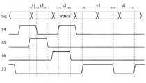
図9に、図8に示す画素11に接続される配線54乃至配線57の電位と、配線21に供
給される画像信号Sigの電位のタイミングチャートを例示する。なお、図9に示すタイ
ミングチャートは、図8に示す画素11に含まれるトランジスタが全てnチャネル型であ
る場合を例示するものである。また、図10乃至図12に、各期間における、画素11の
動作を模式的に示す。ただし、図10乃至図12では、画素11の動作を分かりやすく示
すために、トランジスタ15以外のトランジスタを、スイッチとして図示する。FIG. 9 illustrates a timing chart of the potentials of the
まず、期間t1では、配線54にハイレベルの電位が与えられ、配線55にハイレベルの
電位が与えられ、配線56にローレベルの電位が与えられ、配線57にローレベルの電位
が与えられる。よって、図10(A)に示すように、トランジスタ51、トランジスタ1
6t、トランジスタ17tがオンとなり、トランジスタ50、トランジスタ52はオフと
なる。上記動作により、トランジスタ15のゲートには、配線23の電位Vi2が与えら
れ、トランジスタ15のソース及びドレインの一方には、配線22の電位Vi1が与えら
れる。First, in the period t1, the
6t, the
なお、電位Vi1は、電位Vcatに発光素子14の閾値電圧Vtheを加算した電位よ
りも低いことが望ましい。また、電位Vi2は、トランジスタ15の閾値電圧Vthを電
位Vi1に加算した電位よりも、高いことが望ましい。よって、トランジスタ15のゲー
ト電圧はVi2−Vi1となり、トランジスタ15はオンになる。Note that the potential Vi1 is preferably lower than the potential obtained by adding the threshold voltage Vthe of the
また、配線19には電位Vi1が与えられ、配線20には電位Vcatが与えられる。The
次いで、期間t2では、配線54にローレベルの電位が与えられ、配線55にハイレベル
の電位が与えられ、配線56にローレベルの電位が与えられ、配線57にローレベルの電
位が与えられる。よって、図10(B)に示すように、トランジスタ16t、トランジス
タ51がオンとなり、トランジスタ50、トランジスタ52、トランジスタ17tはオフ
となる。上記動作により、トランジスタ15のゲートに、電位Vi2が保持される。また
、配線19には電位Vi2が与えられ、配線20には電位Vcatが与えられる。Next, in the period t2, the
上記動作により、オンであるトランジスタ15を介して容量素子18の電荷が放出され、
電位Vi1だった、トランジスタ15のソース及びドレインの一方の電位が上昇を始める
。そして、最終的には、トランジスタ15のソース及びドレインの一方の電位がVi2−
Vthに収束し、トランジスタ15のゲート電圧が閾値電圧Vthに収束すると、トラン
ジスタ15がオフになる。By the above operation, the charge of the
The potential of one of the source and the drain of the
When it converges to Vth and the gate voltage of the
なお、図8に示す画素構成では、電位Vi2を、電位Vcatに発光素子14の閾値電圧
Vtheを加算した値より高くしても、トランジスタ52がオフである限り、発光素子1
4は発光しない。そのため、電位Vi1として設定できる値の幅を広げることが可能とな
り、Vi2−Vi1として取りうる値の幅も広げることが可能となる。したがって、Vi
2−Vi1の値の設定の自由度が上がるため、トランジスタ15の閾値電圧の取得に要す
る時間を短縮した場合、または閾値電圧の取得期間に制限がある場合においても、正確に
トランジスタ15の閾値電圧の取得を行うことができる。Note that in the pixel configuration illustrated in FIG. 8, even when the potential Vi2 is higher than the value obtained by adding the threshold voltage Vthe of the
4 does not emit light. Therefore, the range of values that can be set as the potential Vi1 can be widened, and the range of values that can be taken as Vi2-Vi1 can also be widened. Therefore, Vi
Since the degree of freedom in setting the value of 2-Vi1 is increased, the threshold voltage of the
次いで、期間t3では、配線54にハイレベルの電位が与えられ、配線55にローレベル
の電位が与えられ、配線56にハイレベルの電位が与えられ、配線57にローレベルの電
位が与えられる。よって、図11(A)に示すように、トランジスタ50、トランジスタ
17tがオンとなり、トランジスタ51、トランジスタ52、トランジスタ16tはオフ
となる。そして、配線21には画像信号Sigの電位Vdataが与えられ、上記電位V
dataは、トランジスタ50を介して、容量素子18の一対の電極のうちの一方に与え
られる。Next, in a period t3, the
Data is given to one of the pair of electrodes of the
トランジスタ16tがオフであるため、トランジスタ15のゲートはフローティングの状
態にある。また、容量素子18には閾値電圧Vthが保持されているため、容量素子18
の一対の電極のうちの一方に電位Vdataが与えられると、電荷保存の法則に従い、容
量素子18の一対の電極のうちの他方に接続された、トランジスタ15のゲートの電位は
、Vdata+Vthとなる。また、配線22の電位Vi1が、トランジスタ17tを介
してトランジスタ15のソース及びドレインの一方に与えられる。よって、容量素子53
には電圧Vdata−Vi1が印加され、トランジスタ15のゲート電圧は、Vth+V
data−Vi1となる。Since the
When the potential Vdata is applied to one of the pair of electrodes of, the potential of the gate of the
Is applied with a voltage Vdata-Vi1, and the gate voltage of the
data-Vi1.
なお、期間t2から期間t3に移行する際、配線55に与える電位がハイレベルからロー
レベルに切り替えられてから、配線56に与える電位をローレベルからハイレベルに切り
替えることが望ましい。上記構成により、配線56に与える電位の切り替えによって、ト
ランジスタ15のゲートにおける電位の変動を防ぐことができる。Note that when transitioning from the period t2 to the period t3, it is preferable that the potential applied to the
次いで、期間t4では、配線54にローレベルの電位が与えられ、配線55にローレベル
の電位が与えられ、配線56にローレベルの電位が与えられ、配線57にハイレベルの電
位が与えられる。よって、図11(B)に示すように、トランジスタ52がオンとなり、
トランジスタ50、トランジスタ51、トランジスタ16t及びトランジスタ17tがオ
フとなる。Next, in a period t4, the
The
また、配線19には電位Vi2が与えられ、配線20には電位Vcatが与えられる。Further, the
上記動作により、容量素子18に閾値電圧Vthが保持され、容量素子53に電圧Vda
ta−Vi1が保持され、発光素子14の陽極は電位Velとなり、トランジスタ15の
ゲートの電位は電位Vdata+Vth+Vel−Vi1となり、トランジスタ15のゲ
ート電圧はVdata+Vth−Vi1となる。With the above operation, the threshold voltage Vth is held in the
ta-Vi1 is held, the anode of the
なお、電位Velは、トランジスタ15を介して、発光素子14に電流を流す際に設定さ
れる電位である。具体的には、電位Vi2と電位Vcatの間の電位に設定されることと
なる。Note that the potential Vel is a potential set when a current is passed through the
よって、トランジスタ15のゲート電圧を、閾値電圧Vthが加味された値に設定するこ
とができる。上記構成により、トランジスタ15の閾値電圧Vthのばらつきを抑制する
ことができるので、発光素子14に供給する電流値のばらつきを抑え、発光装置の輝度ム
ラを低減することができる。Therefore, the gate voltage of the
なお、配線57に与える電位の変動を大きくしておくことで、トランジスタ52の閾値電
圧のばらつきが発光素子14に供給する電流値に影響を及ぼすことを防ぐことができる。
つまり、配線57に与えるハイレベルの電位をトランジスタ52の閾値電圧よりも十分大
きく、また、配線57に与えるローレベルの電位をトランジスタ52の閾値電圧よりも十
分小さくしてやることで、トランジスタ52のオンとオフの切り替えを確実に行い、トラ
ンジスタ52の閾値電圧のばらつきが発光素子14の電流値に影響を及ぼすことを防ぐこ
とができる。Note that by increasing the fluctuation of the potential applied to the
That is, the high-level potential applied to the
次いで、期間t5では、配線54にハイレベルの電位が与えられ、配線55にローレベル
の電位が与えられ、配線56にローレベルの電位が与えられ、配線57にローレベルの電
位が与えられる。よって、図12に示すように、トランジスタ17tがオンとなり、トラ
ンジスタ16t、トランジスタ50、トランジスタ51及びトランジスタ52がオフとな
る。Next, in a period t5, the
また、配線19には電位Vi2が与えられ、配線22は、モニター回路に接続される。The potential Vi2 is applied to the
上記動作により、トランジスタ15のドレイン電流Idが、発光素子14ではなく、トラ
ンジスタ17tを介して配線22に流れる。モニター回路は、配線22に流れたドレイン
電流Idを用いて、当該ドレイン電流Idの値を情報として含む信号を生成する。そして
、本発明の一態様にかかる発光装置では、上記信号を用いて、画素11に供給される画像
信号Vsigの電位Vdataの値を、補正することができる。By the above operation, the drain current Id of the
なお、図8に示す画素11を有する発光装置では、期間t3の動作の後に期間t4の動作
を常に行う必要はない。例えば、発光装置において、期間t1乃至期間t4の動作を複数
回繰り返した後に、期間t5の動作を行うようにしても良い。また、一行の画素11にお
いて期間t5の動作を行った後、最小の階調値0に対応する画像信号を、当該動作を行っ
た一行の画素11に書き込むことで、発光素子14を非発光の状態にした後、次の行の画
素11において、期間t4の動作を行うようにしても良い。Note that in the light-emitting device including the
図8に示した画素11を有する発光装置では、トランジスタ15のソース及びドレインの
他方と、トランジスタ15のゲートとが電気的に分離しているので、それぞれの電位を個
別に制御することができる。よって、期間t2において、トランジスタ15のソース及び
ドレインの他方の電位を、トランジスタ15のゲートの電位に、閾値電圧Vthを加算し
た電位よりも高い値に設定することができる。そのため、トランジスタ15がノーマリオ
ンである場合に、すなわち閾値電圧Vthがマイナスの値を有している場合に、トランジ
スタ15において、ソースの電位がゲートの電位よりも高くなるまで、容量素子18に電
荷を蓄積することができる。よって、本発明の一態様に係る発光装置では、トランジスタ
15がノーマリオンであっても、期間t2において閾値電圧を取得することができ、期間
t4において、閾値電圧Vthを加味した値になるよう、トランジスタ15のゲート電圧
を設定することができる。In the light emitting device having the
したがって、本発明の一態様に係る発光装置では、例えばトランジスタ15の半導体膜に
酸化物半導体を用いた場合などに、トランジスタ15がノーマリオンとなっても、表示ム
ラを低減でき、高い画質の表示を行うことができる。Therefore, in the light-emitting device according to one embodiment of the present invention, for example, when an oxide semiconductor is used for the semiconductor film of the
〈モニター回路の構成例〉
次いで、モニター回路12の構成例を図13に示す。図13に示すモニター回路12は、
オペアンプ60と、容量素子61と、スイッチ62とを有する。<Example of monitor circuit configuration>
Next, FIG. 13 shows a configuration example of the
It has an
容量素子61が有する一対の電極の一方は、オペアンプ60の反転入力端子(−)に接続
され、容量素子61が有する一対の電極の他方は、オペアンプ60の出力端子に接続され
ている。スイッチ62は、容量素子61に蓄積されている電荷を放出させる機能を有して
おり、具体的には、容量素子61が有する一対の電極間の電気的な接続を制御する機能を
有する。オペアンプ60の非反転入力端子(+)には、バイアス電位VLが供給されてい
る。One of the pair of electrodes of the
図13に示すモニター回路12では、スイッチ62がオフの状態において、画素11から
取り出されたドレイン電流が、モニター回路12の入力端子INに供給されると、容量素
子61に電荷が蓄積され、容量素子61が有する一対の電極間に電圧が生じる。上記電圧
は、入力端子INに供給されたドレイン電流の総量に比例するので、出力端子OUTには
、所定の期間内におけるドレイン電流の総量に対応した電位が、与えられる。In the
〈発光装置の断面構造〉
図14に、本発明の一態様に係る発光装置の、画素部の断面構造を一例として示す。なお
、図14では、図4に示すトランジスタ42、容量素子18、及び発光素子14の、断面
構造を例示している。<Cross-sectional structure of light emitting device>
FIG. 14 illustrates an example of a cross-sectional structure of a pixel portion in a light-emitting device according to one embodiment of the present invention. Note that FIG. 14 illustrates a cross-sectional structure of the
具体的に、図14に示す発光装置は、基板400上にトランジスタ42と、容量素子18
とを有する。トランジスタ42は、ゲートとして機能する導電膜401と、導電膜401
上の絶縁膜402と、絶縁膜402を間に挟んで導電膜401と重なる半導体膜403と
、半導体膜403に電気的に接続されたソースまたはドレインとして機能する導電膜40
4及び導電膜405とを有する。Specifically, in the light emitting device shown in FIG. 14, the
Have and. The
The upper
4 and the
容量素子18は、電極として機能する導電膜410と、導電膜410上の絶縁膜402と
、絶縁膜402を間に挟んで導電膜410と重なり、なおかつ電極として機能する導電膜
405とを有する。The
絶縁膜402としては、酸化アルミニウム、酸化マグネシウム、酸化珪素、酸化窒化珪素
、窒化酸化珪素、窒化珪素、酸化ガリウム、酸化ゲルマニウム、酸化イットリウム、酸化
ジルコニウム、酸化ランタン、酸化ネオジム、酸化ハフニウム及び酸化タンタルを一種以
上含む絶縁膜を、単層で、または積層させて用いればよい。なお、本明細書中において、
酸化窒化物は、その組成として、窒素よりも酸素の含有量が多い材料を指し、窒化酸化物
は、その組成として、酸素よりも窒素の含有量が多い材料を指す。As the insulating
Oxynitride refers to a material having a higher oxygen content than nitrogen as its composition, and nitride oxide refers to a material having a higher nitrogen content than oxygen as its composition.
また、半導体膜403、導電膜404、及び導電膜405上には絶縁膜411が設けられ
ている。半導体膜403として酸化物半導体を用いる場合、絶縁膜411は、半導体膜4
03に酸素を供給させることが可能な材料を用いることが望ましい。上記材料を絶縁膜4
11に用いることで、絶縁膜411に含まれる酸素を半導体膜403に移動させることが
可能であり、半導体膜403の酸素欠損量を低減することができる。絶縁膜411に含ま
れる酸素の半導体膜403への移動は、絶縁膜411を形成した後に、加熱処理を行うこ
とで効率的に行うことができる。An insulating
It is desirable to use a material capable of supplying oxygen to 03. Insulating film 4 with the above materials
When used for No. 11, oxygen contained in the insulating
絶縁膜411上には絶縁膜420が設けられており、絶縁膜420上には導電膜424が
設けられている。導電膜424は、絶縁膜411及び絶縁膜420に設けられた開口部に
おいて、導電膜404に接続されている。The insulating
絶縁膜420及び導電膜424上には絶縁膜425が設けられている。絶縁膜425は、
導電膜424と重なる位置に開口部を有する。また、絶縁膜425上において、絶縁膜4
25の開口部とは異なる位置に、絶縁膜426が設けられている。そして、絶縁膜425
及び絶縁膜426上には、EL層427及び導電膜428が、順に積層するように設けら
れている。導電膜424及び導電膜428が、EL層427を間に挟んで重なり合う部分
が、発光素子14として機能する。そして、導電膜424及び導電膜428は、一方が陽
極、他方が陰極として機能する。An insulating
An opening is provided at a position overlapping with the
An insulating
The
また、発光装置は、発光素子14を間に挟んで基板400と対峙する、基板430を有す
る。基板430上、すなわち、基板430の発光素子14に近い側の面上には、光を遮蔽
する機能を有する遮蔽膜431が設けられている。そして、遮蔽膜431は、発光素子1
4と重なる領域に開口部を有している。発光素子14に重なる開口部において、基板43
0上には特定の波長範囲の可視光を透過する着色層432が設けられている。In addition, the light emitting device includes a
4 has an opening in a region overlapping with 4. In the opening overlapping the
A colored layer 432 that transmits visible light in a specific wavelength range is provided on the
〈トランジスタの構造〉
次いで、酸化物半導体膜にチャネル形成領域を有するトランジスタ70の構成を、一例と
して示す。<Structure of transistor>
Next, the structure of the
図15(A)に示すトランジスタ70は、ゲートとして機能する導電膜80と、導電膜8
0上の絶縁膜81と、絶縁膜81を間に挟んで導電膜80と重なる酸化物半導体膜82と
、酸化物半導体膜82に接続された、ソース及びドレインとして機能する導電膜83及び
導電膜84とを有する。また、図15(A)に示すトランジスタ70は、酸化物半導体膜
82、導電膜83及び導電膜84上に、順に積層された絶縁膜85乃至絶縁膜87を有す
る。A
0, an insulating
なお、図15(A)では、酸化物半導体膜82、導電膜83及び導電膜84上に、順に積
層された絶縁膜85乃至絶縁膜87が設けられている場合を例示しているが、酸化物半導
体膜82、導電膜83及び導電膜84上に設けられる絶縁膜は、一層であっても良いし、
3以上の複数層であっても良い。Note that although FIG. 15A illustrates the case where the insulating
It may be a plurality of layers of three or more.
絶縁膜86は、化学量論的組成以上の酸素が含まれており、加熱により上記酸素の一部を
酸化物半導体膜82に供給する機能を有する絶縁膜であることが望ましい。また、絶縁膜
86は、欠陥が少ないことが好ましく、代表的には、ESR測定により得られる、シリコ
ンのダングリングボンドに由来するg=2.001を持つスピンの密度が1×10¹⁸s
pins/cm3以下であることが好ましい。ただし、絶縁膜86を酸化物半導体膜82
上に直接設けると、絶縁膜86の形成時に酸化物半導体膜82にダメージが与えられる場
合、図15(A)に示すように、絶縁膜85を酸化物半導体膜82と絶縁膜86の間に設
けると良い。絶縁膜85は、その形成時に酸化物半導体膜82に与えるダメージが絶縁膜
86の場合よりも小さく、なおかつ、酸素を透過する機能を有する絶縁膜であることが望
ましい。ただし、酸化物半導体膜82に与えられるダメージを小さく抑えつつ、酸化物半
導体膜82上に絶縁膜86を直接形成することができるのであれば、絶縁膜85は必ずし
も設けなくとも良い。The insulating
It is preferably at most pins/cm3 . However, the insulating
If the
絶縁膜85は、欠陥が少ないことが好ましく、代表的には、ESR測定により得られる、
シリコンのダングリングボンドに由来するg=2.001を持つスピンの密度が3×10
17spins/cm3以下であることが好ましい。これは、絶縁膜85に含まれる欠陥
密度が多いと、当該欠陥に酸素が結合してしまい、絶縁膜85における酸素の透過量が減
少してしまうためである。The insulating
The density of spins having g=2.001 derived from the dangling bond of silicon is 3×10.
It is preferably17 spins/cm3 or less. This is because if the density of defects in the insulating
また、絶縁膜85と酸化物半導体膜82との界面に欠陥が少ないことが好ましく、代表的
には、磁場の向きを膜面に対して平行に印加したESR測定により、酸化物半導体膜82
に用いられる酸化物半導体中の酸素欠損に由来するg値が1.89以上1.96以下であ
るスピンの密度が1×10¹⁷spins/cm3以下、更には検出下限以下であること
が好ましい。In addition, it is preferable that the interface between the insulating
It is preferable that the g value derived from oxygen deficiency in the oxide semiconductor used for is 1.89 or more and 1.96 or less, the density of spins is 1×10¹⁷ spins/cm3 or less, and further is the detection lower limit or less. ..
また、絶縁膜87は、酸素、水素、水の拡散を防ぐブロッキング効果を有することが、望
ましい。或いは、絶縁膜87は、水素、水の拡散を防ぐブロッキング効果を有することが
、望ましい。In addition, it is desirable that the insulating
絶縁膜は、密度が高くて緻密である程、また未結合手が少なく化学的に安定である程、よ
り高いブロッキング効果を示す。酸素、水素、水の拡散を防ぐブロッキング効果を示す絶
縁膜は、例えば、酸化アルミニウム、酸化窒化アルミニウム、酸化ガリウム、酸化窒化ガ
リウム、酸化イットリウム、酸化窒化イットリウム、酸化ハフニウム、酸化窒化ハフニウ
ム等を用いて、形成することができる。水素、水の拡散を防ぐブロッキング効果を示す絶
縁膜は、例えば、窒化シリコン、窒化酸化シリコン等を用いることができる。The insulating film has a higher blocking effect as the density is higher and the density is higher and the number of dangling bonds is smaller and the insulating film is chemically stable. Oxygen, hydrogen, an insulating film showing a blocking effect to prevent the diffusion of water, for example, using aluminum oxide, aluminum oxynitride, gallium oxide, gallium oxynitride, yttrium oxide, yttrium oxynitride, hafnium oxide, hafnium oxynitride, etc. Can be formed. As the insulating film having a blocking effect of preventing diffusion of hydrogen and water, for example, silicon nitride, silicon nitride oxide, or the like can be used.
絶縁膜87が水、水素などの拡散を防ぐブロッキング効果を有する場合、パネル内の樹脂
や、パネルの外部に存在する水、水素などの不純物が、酸化物半導体膜82に侵入するの
を防ぐことができる。酸化物半導体膜82に酸化物半導体を用いる場合、酸化物半導体に
侵入した水または水素の一部は電子供与体(ドナー)となるため、上記ブロッキング効果
を有する絶縁膜87を用いることで、トランジスタ70の閾値電圧がドナーの生成により
シフトするのを防ぐことができる。When the insulating
また、酸化物半導体膜82に酸化物半導体を用いる場合、絶縁膜87が酸素の拡散を防ぐ
ブロッキング効果を有することで、酸化物半導体からの酸素が外部に拡散するのを防ぐこ
とができる。よって、酸化物半導体中において、ドナーとなる酸素欠損が低減されるので
、トランジスタ70の閾値電圧がドナーの生成によりシフトするのを防ぐことができる。When an oxide semiconductor is used for the
なお、図15(A)では、酸化物半導体膜82が、3層の積層された酸化物半導体膜で構
成されている場合を、例示している。具体的に、図15(A)に示すトランジスタ70で
は、酸化物半導体膜82として、酸化物半導体膜82a乃至酸化物半導体膜82cが、絶
縁膜81側から順に積層されている。トランジスタ70の酸化物半導体膜82は、積層さ
れた複数の酸化物半導体膜で構成されているとは限らず、単膜の酸化物半導体膜で構成さ
れていても良い。Note that FIG. 15A illustrates the case where the
そして、酸化物半導体膜82a及び酸化物半導体膜82cは、酸化物半導体膜82bを構
成する金属元素の少なくとも1つを、その構成要素に含み、伝導帯下端のエネルギーが酸
化物半導体膜82bよりも0.05eV以上、0.07eV以上、0.1eV以上又は0
.15eV以上、かつ2eV以下、1eV以下、0.5eV以下又は0.4eV以下、真
空準位に近い酸化物膜である。さらに、酸化物半導体膜82bは、少なくともインジウム
を含むと、キャリア移動度が高くなるため好ましい。The
. It is an oxide film having a vacuum level of 15 eV or higher and 2 eV or lower, 1 eV or lower, 0.5 eV or lower, or 0.4 eV or lower, which is close to a vacuum level. Further, the
また、図15(B)に示すように、トランジスタ70は、酸化物半導体膜82cが導電膜
83及び導電膜84の上層で絶縁膜85と重畳するように設けられている構成を、有して
いてもよい。Further, as illustrated in FIG. 15B, the
なお、電子供与体(ドナー)となる水分または水素などの不純物が低減され、なおかつ酸
素欠損が低減されることにより高純度化された酸化物半導体(purified Oxi
de Semiconductor)は、キャリア発生源が少ないため、i型(真性半導
体)又はi型に限りなく近くすることができる。そのため、高純度化された酸化物半導体
膜にチャネル形成領域を有するトランジスタは、オフ電流が著しく小さく、信頼性が高い
。そして、当該酸化物半導体膜にチャネル形成領域が形成されるトランジスタは、閾値電
圧がプラスとなる電気的特性(ノーマリーオフ特性ともいう。)になりやすい。Note that highly purified oxide semiconductors (purified Oxi) are obtained by reducing impurities such as moisture or hydrogen serving as an electron donor (donor) and reducing oxygen vacancies.
Since the de Semiconductor has a small number of carrier generation sources, it can be as close as possible to i-type (intrinsic semiconductor) or i-type. Therefore, a transistor including a channel formation region in a highly purified oxide semiconductor film has extremely low off-state current and high reliability. A transistor in which a channel formation region is formed in the oxide semiconductor film is likely to have positive threshold voltage (also referred to as normally-off characteristics).
具体的に、高純度化された酸化物半導体膜にチャネル形成領域を有するトランジスタのオ
フ電流が小さいことは、いろいろな実験により証明できる。例えば、チャネル幅が1×1
06μmでチャネル長が10μmの素子であっても、ソース電極とドレイン電極間の電圧
(ドレイン電圧)が1Vから10Vの範囲において、オフ電流が、半導体パラメータアナ
ライザの測定限界以下、すなわち1×10⁻¹³A以下という特性を得ることができる。
この場合、トランジスタのチャネル幅で規格化したオフ電流は、100zA/μm以下で
あることが分かる。また、容量素子とトランジスタとを接続して、容量素子に流入または
容量素子から流出する電荷を当該トランジスタで制御する回路を用いて、オフ電流の測定
を行った。当該測定では、高純度化された酸化物半導体膜を上記トランジスタのチャネル
形成領域に用い、容量素子の単位時間あたりの電荷量の推移から当該トランジスタのオフ
電流を測定した。その結果、トランジスタのソース電極とドレイン電極間の電圧が3Vの
場合に、数十yA/μmという、さらに小さいオフ電流が得られることが分かった。従っ
て、高純度化された酸化物半導体膜をチャネル形成領域に用いたトランジスタは、オフ電
流が、結晶性を有するシリコンを用いたトランジスタに比べて著しく小さい。Specifically, various experiments can prove that the off-state current of a transistor including a channel formation region in a highly purified oxide semiconductor film is small. For example, if the channel width is 1×1
0 even channel length at6 [mu] m is an element of 10 [mu] m, in the voltage (drain voltage) range of 1V to 10V between the source electrode and the drain electrode, the off current is lower than the detection limit of a semiconductor parameter analyzer, i.e. 1 × A characteristic of 10−13 A or less can be obtained.
In this case, it is found that the off-state current standardized by the channel width of the transistor is 100 zA/μm or less. Further, the off-state current was measured using a circuit in which the capacitor and the transistor were connected to each other and the charge flowing into or out of the capacitor was controlled by the transistor. In the measurement, a highly purified oxide semiconductor film was used for the channel formation region of the transistor, and the off-state current of the transistor was measured from the change in the amount of charge of the capacitor per unit time. As a result, it was found that when the voltage between the source electrode and the drain electrode of the transistor was 3 V, an even smaller off current of several tens yA/μm was obtained. Therefore, the off-state current of a transistor including a highly purified oxide semiconductor film in a channel formation region is significantly smaller than that of a transistor including crystalline silicon.
なお、半導体膜として酸化物半導体膜を用いる場合、酸化物半導体としては、少なくとも
インジウム(In)あるいは亜鉛(Zn)を含むことが好ましい。また、該酸化物半導体
を用いたトランジスタの電気的特性のばらつきを減らすためのスタビライザーとして、そ
れらに加えてガリウム(Ga)を有することが好ましい。また、スタビライザーとしてス
ズ(Sn)を有することが好ましい。また、スタビライザーとしてハフニウム(Hf)を
有することが好ましい。また、スタビライザーとしてアルミニウム(Al)を有すること
が好ましい。また、スタビライザーとしてジルコニウム(Zr)を含むことが好ましい。Note that when an oxide semiconductor film is used as the semiconductor film, the oxide semiconductor preferably contains at least indium (In) or zinc (Zn). Further, gallium (Ga) is preferably contained in addition to the stabilizers for reducing variations in electrical characteristics of a transistor including the oxide semiconductor. Moreover, it is preferable to have tin (Sn) as a stabilizer. Further, it is preferable to have hafnium (Hf) as a stabilizer. Further, it is preferable to have aluminum (Al) as the stabilizer. Further, it is preferable that zirconium (Zr) is contained as the stabilizer.
酸化物半導体の中でもIn−Ga−Zn系酸化物、In−Sn−Zn系酸化物などは、炭
化シリコン、窒化ガリウム、または酸化ガリウムとは異なり、スパッタリング法や湿式法
により電気的特性の優れたトランジスタを作製することが可能であり、量産性に優れると
いった利点がある。また、炭化シリコン、窒化ガリウム、または酸化ガリウムとは異なり
、上記In−Ga−Zn系酸化物は、ガラス基板上に、電気的特性の優れたトランジスタ
を作製することが可能である。また、基板の大型化にも対応が可能である。Among oxide semiconductors, In-Ga-Zn-based oxides, In-Sn-Zn-based oxides, and the like have excellent electrical characteristics by a sputtering method or a wet method, unlike silicon carbide, gallium nitride, or gallium oxide. It is possible to manufacture a transistor and has an advantage of being excellent in mass productivity. Further, unlike silicon carbide, gallium nitride, or gallium oxide, the above In—Ga—Zn-based oxide can manufacture a transistor with excellent electrical characteristics over a glass substrate. Further, it is possible to cope with the increase in size of the substrate.
また、他のスタビライザーとして、ランタノイドである、ランタン(La)、セリウム(
Ce)、プラセオジム(Pr)、ネオジム(Nd)、サマリウム(Sm)、ユウロピウム
(Eu)、ガドリニウム(Gd)、テルビウム(Tb)、ジスプロシウム(Dy)、ホル
ミウム(Ho)、エルビウム(Er)、ツリウム(Tm)、イッテルビウム(Yb)、ル
テチウム(Lu)のいずれか一種または複数種を含んでいてもよい。In addition, as other stabilizers, lanthanoids such as lanthanum (La) and cerium (
Ce), praseodymium (Pr), neodymium (Nd), samarium (Sm), europium (Eu), gadolinium (Gd), terbium (Tb), dysprosium (Dy), holmium (Ho), erbium (Er), thulium (Ce). Tm), ytterbium (Yb), or lutetium (Lu) may be contained alone or in combination.
例えば、酸化物半導体として、酸化インジウム、酸化ガリウム、酸化スズ、酸化亜鉛、I
n−Zn系酸化物、Sn−Zn系酸化物、Al−Zn系酸化物、Zn−Mg系酸化物、S
n−Mg系酸化物、In−Mg系酸化物、In−Ga系酸化物、In−Ga−Zn系酸化
物(IGZOとも表記する)、In−Al−Zn系酸化物、In−Sn−Zn系酸化物、
Sn−Ga−Zn系酸化物、Al−Ga−Zn系酸化物、Sn−Al−Zn系酸化物、I
n−Hf−Zn系酸化物、In−La−Zn系酸化物、In−Pr−Zn系酸化物、In
−Nd−Zn系酸化物、In−Ce−Zn系酸化物、In−Sm−Zn系酸化物、In−
Eu−Zn系酸化物、In−Gd−Zn系酸化物、In−Tb−Zn系酸化物、In−D
y−Zn系酸化物、In−Ho−Zn系酸化物、In−Er−Zn系酸化物、In−Tm
−Zn系酸化物、In−Yb−Zn系酸化物、In−Lu−Zn系酸化物、In−Sn−
Ga−Zn系酸化物、In−Hf−Ga−Zn系酸化物、In−Al−Ga−Zn系酸化
物、In−Sn−Al−Zn系酸化物、In−Sn−Hf−Zn系酸化物、In−Hf−
Al−Zn系酸化物を用いることができる。For example, as an oxide semiconductor, indium oxide, gallium oxide, tin oxide, zinc oxide, I
n-Zn-based oxide, Sn-Zn-based oxide, Al-Zn-based oxide, Zn-Mg-based oxide, S
n-Mg-based oxide, In-Mg-based oxide, In-Ga-based oxide, In-Ga-Zn-based oxide (also referred to as IGZO), In-Al-Zn-based oxide, In-Sn-Zn. Oxides,
Sn-Ga-Zn-based oxide, Al-Ga-Zn-based oxide, Sn-Al-Zn-based oxide, I
n-Hf-Zn-based oxide, In-La-Zn-based oxide, In-Pr-Zn-based oxide, In
-Nd-Zn-based oxide, In-Ce-Zn-based oxide, In-Sm-Zn-based oxide, In-
Eu-Zn-based oxide, In-Gd-Zn-based oxide, In-Tb-Zn-based oxide, In-D
y-Zn-based oxide, In-Ho-Zn-based oxide, In-Er-Zn-based oxide, In-Tm
-Zn-based oxide, In-Yb-Zn-based oxide, In-Lu-Zn-based oxide, In-Sn-
Ga-Zn-based oxide, In-Hf-Ga-Zn-based oxide, In-Al-Ga-Zn-based oxide, In-Sn-Al-Zn-based oxide, In-Sn-Hf-Zn-based oxide , In-Hf-
An Al-Zn oxide can be used.
なお、例えば、In−Ga−Zn系酸化物とは、InとGaとZnを含む酸化物という意
味であり、InとGaとZnの比率は問わない。また、InとGaとZn以外の金属元素
を含んでいてもよい。In−Ga−Zn系酸化物は、無電界時の抵抗が十分に高くオフ電
流を十分に小さくすることが可能であり、また、移動度も高い。Note that, for example, an In—Ga—Zn-based oxide means an oxide containing In, Ga, and Zn, and the ratio of In, Ga, and Zn does not matter. Further, it may contain a metal element other than In, Ga, and Zn. The In—Ga—Zn-based oxide has a sufficiently high resistance in the absence of an electric field, can sufficiently reduce the off current, and has a high mobility.
例えば、In−Sn−Zn系酸化物では比較的容易に高い移動度が得られる。しかしなが
ら、In−Ga−Zn系酸化物でも、バルク内欠陥密度を低減することにより移動度を上
げることができる。For example, with an In—Sn—Zn-based oxide, high mobility can be relatively easily obtained. However, even with an In-Ga-Zn-based oxide, mobility can be increased by reducing the defect density in the bulk.
以下では、酸化物半導体膜の構造について説明する。The structure of the oxide semiconductor film is described below.
酸化物半導体膜は、単結晶酸化物半導体膜と非単結晶酸化物半導体膜とに大別される。非
単結晶酸化物半導体膜とは、非晶質酸化物半導体膜、微結晶酸化物半導体膜、多結晶酸化
物半導体膜、CAAC−OS膜などをいう。The oxide semiconductor film is roughly classified into a single crystal oxide semiconductor film and a non-single crystal oxide semiconductor film. The non-single-crystal oxide semiconductor film refers to an amorphous oxide semiconductor film, a microcrystalline oxide semiconductor film, a polycrystalline oxide semiconductor film, a CAAC-OS film, or the like.
非晶質酸化物半導体膜は、膜中における原子配列が不規則であり、結晶成分を有さない酸
化物半導体膜である。微小領域においても結晶部を有さず、膜全体が完全な非晶質構造の
酸化物半導体膜が典型である。The amorphous oxide semiconductor film is an oxide semiconductor film in which the atomic arrangement in the film is irregular and has no crystal component. An oxide semiconductor film having an amorphous structure in which the entire film does not have a crystal part even in a minute region and is complete is typical.
微結晶酸化物半導体膜は、例えば、1nm以上10nm未満の大きさの微結晶(ナノ結晶
ともいう。)を含む。従って、微結晶酸化物半導体膜は、非晶質酸化物半導体膜よりも原
子配列の規則性が高い。そのため、微結晶酸化物半導体膜は、非晶質酸化物半導体膜より
も欠陥準位密度が低いという特徴がある。The microcrystalline oxide semiconductor film contains, for example, microcrystals (also referred to as nanocrystals) each having a size of 1 nm to less than 10 nm. Therefore, the microcrystalline oxide semiconductor film has higher regularity of atomic arrangement than the amorphous oxide semiconductor film. Therefore, the microcrystalline oxide semiconductor film has a feature that the density of defect states is lower than that of the amorphous oxide semiconductor film.
CAAC−OS膜は、複数の結晶部を有する酸化物半導体膜の一つであり、ほとんどの結
晶部は、一辺が100nm未満の立方体内に収まる大きさである。従って、CAAC−O
S膜に含まれる結晶部は、一辺が10nm未満、5nm未満または3nm未満の立方体内
に収まる大きさの場合も含まれる。CAAC−OS膜は、微結晶酸化物半導体膜よりも欠
陥準位密度が低いという特徴がある。CAAC−OS膜を透過型電子顕微鏡(TEM:T
ransmission Electron Microscope)によって観察する
と、結晶部同士の明確な境界、即ち結晶粒界(グレインバウンダリーともいう。)を確認
することができない。そのため、CAAC−OS膜は、結晶粒界に起因する電子移動度の
低下が起こりにくいといえる。The CAAC-OS film is one of oxide semiconductor films including a plurality of crystal parts, and most of the crystal parts each fit inside a cube whose one side is less than 100 nm. Therefore, CAAC-O
The crystal part included in the S film also includes a case where one side is less than 10 nm, less than 5 nm, or less than 3 nm and fits in a cube. The CAAC-OS film has a feature that the density of defect states is lower than that of the microcrystalline oxide semiconductor film. A CAAC-OS film is formed using a transmission electron microscope (TEM:T).
When observed by a transmission electron microscope, it is not possible to confirm a clear boundary between crystal parts, that is, a crystal grain boundary (also referred to as a grain boundary). Therefore, it can be said that the CAAC-OS film is unlikely to have a decrease in electron mobility due to a crystal grain boundary.
CAAC−OS膜を、試料面と概略平行な方向からTEMによって観察(断面TEM観察
)すると、結晶部において、金属原子が層状に配列していることを確認できる。金属原子
の各層は、CAAC−OS膜の膜を形成する面(被形成面ともいう。)または上面の凹凸
を反映した形状であり、CAAC−OS膜の被形成面または上面と平行に配列する。When the CAAC-OS film is observed with a TEM from a direction substantially parallel to the sample surface (cross-sectional TEM observation), it can be confirmed that metal atoms are arranged in a layered manner in the crystal part. Each layer of metal atoms has a shape that reflects unevenness of the surface (also referred to as a formation surface) of the CAAC-OS film, which is formed, or is aligned in parallel to the formation surface or the top surface of the CAAC-OS film. ..
本明細書において、「平行」とは、二つの直線が−10°以上10°以下の角度で配置さ
れている状態をいう。従って、−5°以上5°以下の場合も含まれる。また、「垂直」と
は、二つの直線が80°以上100°以下の角度で配置されている状態をいう。従って、
85°以上95°以下の場合も含まれる。In this specification, “parallel” means a state in which two straight lines are arranged at an angle of −10° or more and 10° or less. Therefore, a case of -5° or more and 5° or less is also included. Further, “vertical” means a state in which two straight lines are arranged at an angle of 80° or more and 100° or less. Therefore,
The case of 85° or more and 95° or less is also included.
一方、CAAC−OS膜を、試料面と概略垂直な方向からTEMによって観察(平面TE
M観察)すると、結晶部において、金属原子が三角形状または六角形状に配列しているこ
とを確認できる。しかしながら、異なる結晶部間で、金属原子の配列に規則性は見られな
い。On the other hand, the CAAC-OS film is observed by TEM from a direction substantially perpendicular to the sample surface (planar TE
(M observation), it can be confirmed that the metal atoms are arranged in a triangular shape or a hexagonal shape in the crystal part. However, there is no regularity in the arrangement of metal atoms between different crystal parts.
断面TEM観察および平面TEM観察より、CAAC−OS膜の結晶部は配向性を有して
いることがわかる。From cross-sectional TEM observation and plane TEM observation, it is found that the crystal part of the CAAC-OS film has orientation.
CAAC−OS膜に対し、X線回折(XRD:X−Ray Diffraction)装
置を用いて構造解析を行うと、例えばInGaZnO4の結晶を有するCAAC−OS膜
のout−of−plane法による解析では、回折角(2θ)が31°近傍にピークが
現れる場合がある。このピークは、InGaZnO4の結晶の(009)面に帰属される
ことから、CAAC−OS膜の結晶がc軸配向性を有し、c軸が被形成面または上面に概
略垂直な方向を向いていることが確認できる。When the structural analysis of the CAAC-OS film is performed using an X-ray diffraction (XRD: X-Ray Diffraction) apparatus, for example, in the analysis of the CAAC-OS film including a crystal of InGaZnO4 by the out-of-plane method, A peak may appear near the diffraction angle (2θ) of 31°. Since this peak is assigned to the (009) plane of the InGaZnO4 crystal, the crystal of the CAAC-OS film has c-axis orientation, and the c-axis faces a direction substantially perpendicular to the formation surface or the top surface. Can be confirmed.
一方、CAAC−OS膜に対し、c軸に概略垂直な方向からX線を入射させるin−pl
ane法による解析では、2θが56°近傍にピークが現れる場合がある。このピークは
、InGaZnO4の結晶の(110)面に帰属される。InGaZnO4の単結晶酸化
物半導体膜であれば、2θを56°近傍に固定し、試料面の法線ベクトルを軸(φ軸)と
して試料を回転させながら分析(φスキャン)を行うと、(110)面と等価な結晶面に
帰属されるピークが6本観察される。これに対し、CAAC−OS膜の場合は、2θを5
6°近傍に固定してφスキャンした場合でも、明瞭なピークが現れない。On the other hand, the in-pl which causes X-rays to enter the CAAC-OS film from a direction substantially perpendicular to the c-axis
In the analysis by the ane method, a peak may appear near 2θ of 56°. This peak is assigned to the (110) plane of the InGaZnO4 crystal. In the case of an InGaZnO4 single crystal oxide semiconductor film, if 2θ is fixed at around 56° and analysis (φ scan) is performed while rotating the sample with the normal vector of the sample surface as the axis (φ axis), ( Six peaks attributed to a crystal plane equivalent to the (110) plane are observed. On the other hand, in the case of the CAAC-OS film, 2θ is 5
No clear peak appears even when φ scan is performed with the angle fixed at around 6°.
以上のことから、CAAC−OS膜では、異なる結晶部間ではa軸およびb軸の配向は不
規則であるが、c軸配向性を有し、かつc軸が被形成面または上面の法線ベクトルに平行
な方向を向いていることがわかる。従って、前述の断面TEM観察で確認された層状に配
列した金属原子の各層は、結晶のab面に平行な面である。From the above, in the CAAC-OS film, the a-axis and the b-axis are irregularly oriented between different crystal parts, but they have c-axis orientation and the c-axis is a normal to the formation surface or the top surface. It can be seen that the direction is parallel to the vector. Therefore, each layer of the metal atoms arranged in layers, which was confirmed by the above-described cross-sectional TEM observation, is a plane parallel to the ab plane of the crystal.
なお、結晶部は、CAAC−OS膜を成膜した際、または加熱処理などの結晶化処理を行
った際に形成される。上述したように、結晶のc軸は、CAAC−OS膜の被形成面また
は上面の法線ベクトルに平行な方向に配向する。従って、例えば、CAAC−OS膜の形
状をエッチングなどによって変化させた場合、結晶のc軸がCAAC−OS膜の被形成面
または上面の法線ベクトルと平行にならないこともある。Note that the crystal part is formed when the CAAC-OS film is formed or when crystallization treatment such as heat treatment is performed. As described above, the c-axis of the crystal is oriented in a direction parallel to the normal vector of the formation surface or the top surface of the CAAC-OS film. Therefore, for example, when the shape of the CAAC-OS film is changed by etching or the like, the c-axis of the crystal might not be parallel to the normal vector of the formation surface or the upper surface of the CAAC-OS film.
また、CAAC−OS膜中の結晶化度が均一でなくてもよい。例えば、CAAC−OS膜
の結晶部が、CAAC−OS膜の上面近傍からの結晶成長によって形成される場合、上面
近傍の領域は、被形成面近傍の領域よりも結晶化度が高くなることがある。また、CAA
C−OS膜に不純物を添加する場合、不純物が添加された領域の結晶化度が変化し、部分
的に結晶化度の異なる領域が形成されることもある。Further, the crystallinity in the CAAC-OS film may not be uniform. For example, when the crystal part of the CAAC-OS film is formed by crystal growth from the vicinity of the upper surface of the CAAC-OS film, the region near the upper surface has higher crystallinity than the region near the formation surface. is there. Also, CAA
When an impurity is added to the C-OS film, the crystallinity of the region to which the impurity is added may change, and a region with different crystallinity may be partially formed.
なお、InGaZnO4の結晶を有するCAAC−OS膜のout−of−plane法
による解析では、2θが31°近傍のピークの他に、2θが36°近傍にもピークが現れ
る場合がある。2θが36°近傍のピークは、CAAC−OS膜中の一部に、c軸配向性
を有さない結晶が含まれることを示している。CAAC−OS膜は、2θが31°近傍に
ピークを示し、2θが36°近傍にピークを示さないことが好ましい。Note that in the analysis of the CAAC-OS film including an InGaZnO4 crystal by an out-of-plane method, a peak may appear near 2θ of 36° in addition to a peak at 2θ of 31°. The peak near 2θ of 36° indicates that a part of the CAAC-OS film contains a crystal having no c-axis orientation. The CAAC-OS film preferably has a peak at 2θ of around 31° and no peak at 2θ of around 36°.
CAAC−OS膜を用いたトランジスタは、可視光や紫外光の照射による電気的特性の変
動が小さい。よって、当該トランジスタは、信頼性が高い。A transistor including a CAAC-OS film has small variation in electrical characteristics due to irradiation with visible light or ultraviolet light. Therefore, the transistor has high reliability.
なお、酸化物半導体膜は、例えば、非晶質酸化物半導体膜、微結晶酸化物半導体膜、CA
AC−OS膜のうち、二種以上を有する積層膜であってもよい。Note that the oxide semiconductor film is, for example, an amorphous oxide semiconductor film, a microcrystalline oxide semiconductor film, or CA.
A laminated film having two or more kinds of AC-OS films may be used.
また、CAAC−OS膜を成膜するために、以下の条件を適用することが好ましい。In addition, the following conditions are preferably applied to form the CAAC-OS film.
成膜時の不純物混入を低減することで、不純物によって結晶状態が崩れることを抑制でき
る。例えば、処理室内に存在する不純物濃度(水素、水、二酸化炭素、及び窒素など)を
低減すればよい。また、成膜ガス中の不純物濃度を低減すればよい。具体的には、露点が
−80℃以下、好ましくは−100℃以下である成膜ガスを用いる。By reducing the mixture of impurities during the film formation, the crystal state can be prevented from being broken by the impurities. For example, the concentration of impurities (hydrogen, water, carbon dioxide, nitrogen, etc.) existing in the processing chamber may be reduced. Further, the concentration of impurities in the deposition gas may be reduced. Specifically, a deposition gas whose dew point is −80° C. or lower, preferably −100° C. or lower is used.
また、成膜時の基板加熱温度を高めることで、基板到達後にスパッタリング粒子のマイグ
レーションが起こる。具体的には、基板加熱温度を100℃以上740℃以下、好ましく
は200℃以上500℃以下として成膜する。成膜時の基板加熱温度を高めることで、平
板状またはペレット状のスパッタリング粒子が基板に到達した場合、基板上でマイグレー
ションが起こり、スパッタリング粒子の平らな面が基板に付着する。Further, by increasing the substrate heating temperature during film formation, migration of sputtered particles occurs after reaching the substrate. Specifically, the substrate heating temperature is 100° C. or higher and 740° C. or lower, preferably 200° C. or higher and 500° C. or lower. When flat-plate-like or pellet-like sputtered particles reach the substrate by increasing the substrate heating temperature during film formation, migration occurs on the substrate and the flat surface of the sputtered particles adheres to the substrate.
また、成膜ガス中の酸素割合を高め、電力を最適化することで成膜時のプラズマダメージ
を軽減すると好ましい。成膜ガス中の酸素割合は、30体積%以上、好ましくは100体
積%とする。Further, it is preferable that the proportion of oxygen in the deposition gas be increased and the power be optimized in order to reduce plasma damage at the deposition. The proportion of oxygen in the deposition gas is 30% by volume or higher, preferably 100% by volume.
ターゲットの一例として、In−Ga−Zn系酸化物ターゲットについて以下に示す。An In—Ga—Zn-based oxide target is shown below as an example of the target.
InOX粉末、GaOY粉末及びZnOZ粉末を所定のmol数比で混合し、加圧処理後
、1000℃以上1500℃以下の温度で加熱処理をすることで多結晶であるIn−Ga
−Zn系酸化物ターゲットとする。なお、X、Y及びZは任意の正数である。ここで、所
定のmol数比は、例えば、InOX粉末、GaOY粉末及びZnOZ粉末が、2:2:
1、8:4:3、3:1:1、1:1:1、4:2:3、1:4:4または3:1:2で
ある。なお、粉末の種類、及びその混合するmol数比は、作製するターゲットによって
適宜変更すればよい。InOX powder, GaOY powder, and ZnOZ powder are mixed in a predetermined molar ratio, and after pressure treatment, heat treatment is performed at a temperature of 1000° C. or higher and 1500° C. or lower to form polycrystalline In-Ga.
-Use as a Zn-based oxide target. Note that X, Y, and Z are arbitrary positive numbers. Here, the predetermined molar ratio is, for example, 2:2: for InOX powder, GaOY powder and ZnOZ powder.
1, 8:4:3, 3:1:1, 1:1, 4:2:3, 1:4:4 or 3:1:2. Note that the kind of powder and the molar ratio for mixing powder may be changed as appropriate depending on a target to be manufactured.
なお、アルカリ金属は酸化物半導体を構成する元素ではないため、不純物である。アルカ
リ土類金属も、酸化物半導体を構成する元素ではない場合において、不純物となる。特に
、アルカリ金属のうちNaは、酸化物半導体膜に接する絶縁膜が酸化物である場合、当該
絶縁膜中に拡散してNa+となる。また、Naは、酸化物半導体膜内において、酸化物半
導体を構成する金属と酸素の結合を分断する、或いは、その結合中に割り込む。その結果
、例えば、閾値電圧がマイナス方向にシフトすることによるノーマリオン化、移動度の低
下等の、トランジスタの電気的特性の劣化が起こり、加えて、特性のばらつきも生じる。
具体的に、二次イオン質量分析法によるNa濃度の測定値は、5×10¹⁶/cm3以下
、好ましくは1×10¹⁶/cm3以下、更に好ましくは1×1015/cm3以下とす
るとよい。同様に、Li濃度の測定値は、5×10¹⁵/cm3以下、好ましくは1×1
015/cm3以下とするとよい。同様に、K濃度の測定値は、5×1015/cm3以
下、好ましくは1×10¹⁵/cm3以下とするとよい。Note that the alkali metal is an impurity because it is not an element included in the oxide semiconductor. Alkaline earth metal also becomes an impurity when it is not an element forming an oxide semiconductor. In particular, Na among alkali metals diffuses into the insulating film, which is Na+ , when the insulating film in contact with the oxide semiconductor film is an oxide. Further, Na divides the bond between the metal forming the oxide semiconductor and oxygen in the oxide semiconductor film or interrupts the bond. As a result, the electrical characteristics of the transistor are deteriorated, such as a normally-on state due to the threshold voltage being shifted in the negative direction and a reduction in mobility. In addition, characteristic variations are also generated.
Specifically, the measured value of Na concentration by secondary ion mass spectrometry is 5×10¹⁶ /cm3 or less, preferably 1×10¹⁶ /cm3 or less, and more preferably 1×10¹⁵ /cm3 or less. Good to do. Similarly, the measured Li concentration is 5×10¹⁵ /cm3 or less, preferably 1×1.
It is preferable to set it to 015 /cm3 or less. Similarly, the measured K concentration may be 5×10¹⁵ /cm3 or less, preferably 1×10¹⁵ /cm3 or less.
また、インジウムを含む金属酸化物が用いられている場合に、酸素との結合エネルギーが
インジウムよりも大きいシリコンや炭素が、インジウムと酸素の結合を切断し、酸素欠損
を形成することがある。そのため、シリコンや炭素が酸化物半導体膜に混入していると、
アルカリ金属やアルカリ土類金属の場合と同様に、トランジスタの電気的特性の劣化が起
こりやすい。よって、酸化物半導体膜中におけるシリコンや炭素の濃度は低いことが望ま
しい。具体的に、二次イオン質量分析法によるC濃度の測定値、またはSi濃度の測定値
は、1×10¹⁸/cm3以下とするとよい。上記構成により、トランジスタの電気的特
性の劣化を防ぐことができ、半導体装置の信頼性を高めることができる。When a metal oxide containing indium is used, silicon or carbon, which has a bond energy with oxygen larger than that of indium, may break the bond between indium and oxygen to form an oxygen vacancy. Therefore, if silicon or carbon is mixed in the oxide semiconductor film,
As in the case of alkali metal or alkaline earth metal, the electrical characteristics of the transistor are likely to deteriorate. Therefore, it is desirable that the concentration of silicon or carbon in the oxide semiconductor film be low. Specifically, the measured value of C concentration or the measured value of Si concentration by secondary ion mass spectrometry is preferably 1×10¹⁸ /cm3 or less. With the above structure, deterioration in electrical characteristics of the transistor can be prevented and reliability of the semiconductor device can be improved.
また、ソース電極及びドレイン電極に用いられる導電性材料によっては、ソース電極及び
ドレイン電極中の金属が、酸化物半導体膜から酸素を引き抜くことがある。この場合、酸
化物半導体膜のうち、ソース電極及びドレイン電極に接する領域が、酸素欠損の形成によ
りn型化される。Further, depending on the conductive material used for the source electrode and the drain electrode, the metal in the source electrode and the drain electrode might extract oxygen from the oxide semiconductor film. In this case, a region of the oxide semiconductor film, which is in contact with the source electrode and the drain electrode, is made n-type by formation of oxygen vacancies.
n型化された領域は、ソース領域またはドレイン領域として機能するため、酸化物半導体
膜とソース電極及びドレイン電極との間におけるコンタクト抵抗を下げることができる。
よって、n型化された領域が形成されることで、トランジスタの移動度及びオン電流を高
めることができ、それにより、トランジスタを用いた半導体装置の高速動作を実現するこ
とができる。Since the n-type region functions as a source region or a drain region, contact resistance between the oxide semiconductor film and the source and drain electrodes can be reduced.
Therefore, the mobility and on-state current of the transistor can be increased by forming the n-type region, whereby high-speed operation of the semiconductor device including the transistor can be realized.
なお、ソース電極及びドレイン電極中の金属による酸素の引き抜きは、ソース電極及びド
レイン電極をスパッタリング法などにより形成する際に起こりうるし、ソース電極及びド
レイン電極を形成した後に行われる加熱処理によっても起こりうる。Note that extraction of oxygen by the metal in the source electrode and the drain electrode can occur when the source electrode and the drain electrode are formed by a sputtering method or the like, and can also be caused by heat treatment performed after the source electrode and the drain electrode are formed. ..
また、n型化される領域は、酸素と結合し易い導電性材料をソース電極及びドレイン電極
に用いることで、より形成されやすくなる。上記導電性材料としては、例えば、Al、C
r、Cu、Ta、Ti、Mo、Wなどが挙げられる。Further, the n-type region can be formed more easily by using a conductive material that easily bonds with oxygen for the source electrode and the drain electrode. Examples of the conductive material include Al and C
r, Cu, Ta, Ti, Mo, W and the like can be mentioned.
また、酸化物半導体膜は、単数の金属酸化物膜で構成されているとは限らず、積層された
複数の金属酸化物膜で構成されていても良い。例えば、第1乃至第3の金属酸化物膜が順
に積層されている半導体膜の場合、第1の金属酸化物膜及び第3の金属酸化物膜は、第2
の金属酸化物膜を構成する金属元素の少なくとも1つを、その構成要素に含み、伝導帯下
端のエネルギーが第2の金属酸化物膜よりも0.05eV以上、0.07eV以上、0.
1eV以上または0.15eV以上、かつ2eV以下、1eV以下、0.5eV以下また
は0.4eV以下、真空準位に近い酸化物膜である。さらに、第2の金属酸化物膜は、少
なくともインジウムを含むと、キャリア移動度が高くなるため好ましい。In addition, the oxide semiconductor film is not limited to be formed of a single metal oxide film, and may be formed of a plurality of stacked metal oxide films. For example, in the case of a semiconductor film in which first to third metal oxide films are sequentially stacked, the first metal oxide film and the third metal oxide film are
Of the metal oxide film, the energy of the lower end of the conduction band is 0.05 eV or more, 0.07 eV or more, 0.
The oxide film is 1 eV or higher or 0.15 eV or higher and 2 eV or lower, 1 eV or lower, 0.5 eV or lower, or 0.4 eV or lower, which is close to a vacuum level. Further, it is preferable that the second metal oxide film contains at least indium because carrier mobility becomes high.
上記構成の半導体膜をトランジスタが有する場合、ゲート電極に電圧を印加することで、
半導体膜に電界が加わると、半導体膜のうち、伝導帯下端のエネルギーが小さい第2の金
属酸化物膜にチャネル領域が形成される。即ち、第2の金属酸化物膜とゲート絶縁膜との
間に第3の金属酸化物膜が設けられていることによって、ゲート絶縁膜と離隔している第
2の金属酸化物膜に、チャネル領域を形成することができる。When the transistor has the semiconductor film having the above structure, by applying a voltage to the gate electrode,
When an electric field is applied to the semiconductor film, a channel region is formed in the second metal oxide film of the semiconductor film where the energy at the lower end of the conduction band is small. That is, since the third metal oxide film is provided between the second metal oxide film and the gate insulating film, the second metal oxide film separated from the gate insulating film has a channel. Regions can be formed.
また、第3の金属酸化物膜は、第2の金属酸化物膜を構成する金属元素の少なくとも1つ
をその構成要素に含むため、第2の金属酸化物膜と第3の金属酸化物膜の界面では、界面
散乱が起こりにくい。従って、当該界面においてキャリアの動きが阻害されにくいため、
トランジスタの電界効果移動度が高くなる。In addition, since the third metal oxide film contains at least one of the metal elements that form the second metal oxide film as its constituent elements, the second metal oxide film and the third metal oxide film Interface scattering is unlikely to occur at the interface. Therefore, since the movement of the carrier is less likely to be hindered at the interface,
The field effect mobility of the transistor is increased.
また、第2の金属酸化物膜と第1の金属酸化物膜の界面に界面準位が形成されると、界面
近傍の領域にもチャネル領域が形成されるために、トランジスタの閾値電圧が変動してし
まう。しかし、第1の金属酸化物膜は、第2の金属酸化物膜を構成する金属元素の少なく
とも1つをその構成要素に含むため、第2の金属酸化物膜と第1の金属酸化物膜の界面に
は、界面準位が形成されにくい。よって、上記構成により、トランジスタの閾値電圧等の
電気的特性のばらつきを、低減することができる。Further, when an interface state is formed at the interface between the second metal oxide film and the first metal oxide film, a channel region is also formed in a region near the interface, so that the threshold voltage of the transistor varies. Resulting in. However, since the first metal oxide film contains at least one of the metal elements forming the second metal oxide film as its constituent elements, the second metal oxide film and the first metal oxide film It is difficult for an interface level to be formed at the interface. Therefore, with the above structure, variation in electrical characteristics such as the threshold voltage of the transistor can be reduced.
また、金属酸化物膜間に不純物が存在することによって、各膜の界面にキャリアの流れを
阻害する界面準位が形成されることがないよう、複数の酸化物半導体膜を積層させること
が望ましい。積層された金属酸化物膜の膜間に不純物が存在していると、金属酸化物膜間
における伝導帯下端のエネルギーの連続性が失われ、界面近傍において、キャリアがトラ
ップされるか、あるいは再結合により消滅してしまうからである。膜間における不純物を
低減させることで、主成分である一の金属を少なくとも共に有する複数の金属酸化物膜を
、単に積層させるよりも、連続接合(ここでは特に伝導帯下端のエネルギーが各膜の間で
連続的に変化するU字型の井戸構造を有している状態)が形成されやすくなる。In addition, it is preferable that a plurality of oxide semiconductor films be stacked so that an interface state which hinders carrier flow is not formed at the interface between the films due to the presence of impurities between the metal oxide films. .. When impurities are present between the stacked metal oxide films, the continuity of energy at the bottom of the conduction band between the metal oxide films is lost, and carriers are trapped or regenerated near the interface. This is because they disappear when combined. By reducing the impurities between the films, continuous bonding (here, especially the energy at the bottom of the conduction band is higher than that of each film is achieved) rather than simply stacking a plurality of metal oxide films each containing at least one metal which is a main component. (A state having a U-shaped well structure that continuously changes between) is easily formed.
連続接合を形成するためには、ロードロック室を備えたマルチチャンバー方式の成膜装置
(スパッタリング装置)を用いて各膜を大気に触れさせることなく連続して積層すること
が必要となる。スパッタリング装置における各チャンバーは、酸化物半導体にとって不純
物となる水等を可能な限り除去すべくクライオポンプのような吸着式の真空排気ポンプを
用いて高真空排気(5×10⁻⁷Pa乃至1×10⁻⁴Pa程度まで)することが好まし
い。または、ターボ分子ポンプとコールドトラップを組み合わせて排気系からチャンバー
内に気体が逆流しないようにしておくことが好ましい。In order to form a continuous bond, it is necessary to continuously stack the films without exposing them to the atmosphere using a multi-chamber film forming apparatus (sputtering apparatus) equipped with a load lock chamber. In each chamber of the sputtering apparatus, an adsorption type vacuum exhaust pump such as a cryopump is used for high vacuum exhaust (5×10⁻⁷ Pa to 1×) in order to remove water and the like which are impurities in the oxide semiconductor as much as possible. Up to about 10−4 Pa). Alternatively, it is preferable to combine a turbo molecular pump and a cold trap so that gas does not flow backward from the exhaust system into the chamber.
高純度の真性な酸化物半導体を得るためには、各チャンバー内を高真空排気するのみなら
ず、スパッタリングに用いるガスの高純度化も重要である。上記ガスとして用いる酸素ガ
スやアルゴンガスの露点を、−40℃以下、好ましくは−80℃以下、より好ましくは−
100℃以下とし、使用するガスの高純度化を図ることで、酸化物半導体膜に水分等が取
り込まれることを可能な限り防ぐことができる。具体的に、第2の金属酸化物膜がIn−
M−Zn酸化物(Mは、Ga、Y、Zr、La、Ce、またはNd)の場合、第2の金属
酸化物膜を成膜するために用いるターゲットにおいて、金属元素の原子数比をIn:M:
Zn=x1:y1:z1とすると、x1/y1は、1/3以上6以下、さらには1以上6
以下であって、z1/y1は、1/3以上6以下、さらには1以上6以下であることが好
ましい。なお、z1/y1を1以上6以下とすることで、第2の金属酸化物膜としてCA
AC−OS膜が形成されやすくなる。ターゲットの金属元素の原子数比の代表例としては
、In:M:Zn=1:1:1、In:M:Zn=3:1:2等がある。In order to obtain a highly pure intrinsic oxide semiconductor, it is important not only to evacuate each chamber to a high vacuum, but also to highly purify the gas used for sputtering. The dew point of oxygen gas or argon gas used as the above gas is −40° C. or lower, preferably −80° C. or lower, and more preferably −
When the temperature is 100° C. or lower and the gas used is highly purified, moisture and the like can be prevented from being taken into the oxide semiconductor film as much as possible. Specifically, the second metal oxide film is In-
In the case of M-Zn oxide (M is Ga, Y, Zr, La, Ce, or Nd), in the target used for forming the second metal oxide film, the atomic ratio of the metal elements is In. : M:
When Zn=x1 :y1 :z1, x1 /y1 is 1/3 or more and 6 or less, and further 1 or more 6
In the following, z1 /y1 is preferably 1/3 or more and 6 or less, and more preferably 1 or more and 6 or less. Note that by setting z1 /y1 to be 1 or more and 6 or less, CA can be used as the second metal oxide film.
The AC-OS film is easily formed. In:M:Zn=1:1:1, In:M:Zn=3:1:2, and the like are typical examples of the atomic ratio of the target metal element.
具体的に、第1の金属酸化物膜、第3の金属酸化物膜がIn−M−Zn酸化物(Mは、G
a、Y、Zr、La、Ce、またはNd)の場合、第1の金属酸化物膜、第3の金属酸化
物膜を成膜するために用いるターゲットにおいて、金属元素の原子数比をIn:M:Zn
=x2:y2:z2とすると、x2/y2<x1/y1であって、z2/y2は、1/3
以上6以下、さらには1以上6以下であることが好ましい。なお、z2/y2を1以上6
以下とすることで、第1の金属酸化物膜、第3の金属酸化物膜としてCAAC−OS膜が
形成されやすくなる。ターゲットの金属元素の原子数比の代表例としては、In:M:Z
n=1:3:2、In:M:Zn=1:3:4、In:M:Zn=1:3:6、In:M
:Zn=1:3:8等がある。Specifically, the first metal oxide film and the third metal oxide film are In-M-Zn oxide (M is G
a, Y, Zr, La, Ce, or Nd), in the target used for forming the first metal oxide film and the third metal oxide film, the atomic ratio of the metal elements is In: M: Zn
=X2: y2: Whenz2, ax 2 / y 2 <x 1 /
It is preferably 6 or more and 6 or less, more preferably 1 or more and 6 or less. In addition, z2 /y2 is 1 or more and 6
By the following, the CAAC-OS film can be easily formed as the first metal oxide film and the third metal oxide film. As a typical example of the atomic number ratio of the target metal element, In:M:Z
n=1:3:2, In:M:Zn=1:3:4, In:M:Zn=1:3:6, In:M
:Zn=1:3:8 and so on.
なお、第1の金属酸化物膜及び第3の金属酸化物膜の厚さは、3nm以上100nm以下
、好ましくは3nm以上50nm以下とする。また、第2の金属酸化物膜の厚さは、3n
m以上200nm以下、好ましくは3nm以上100nm以下であり、さらに好ましくは
3nm以上50nm以下である。Note that the thickness of the first metal oxide film and the third metal oxide film is 3 nm to 100 nm inclusive, preferably 3 nm to 50 nm inclusive. The thickness of the second metal oxide film is 3n.
m or more and 200 nm or less, preferably 3 nm or more and 100 nm or less, and more preferably 3 nm or more and 50 nm or less.
3層構造の半導体膜において、第1の金属酸化物膜乃至第3の金属酸化物膜は、非晶質ま
たは結晶質の両方の形態を取りうる。ただし、チャネル領域が形成される第2の金属酸化
物膜が結晶質であることにより、トランジスタに安定した電気的特性を付与することがで
きるため、第2の金属酸化物膜は結晶質であることが好ましい。In the semiconductor film having a three-layer structure, the first metal oxide film to the third metal oxide film can be either amorphous or crystalline. However, since the second metal oxide film in which the channel region is formed is crystalline, stable electrical characteristics can be given to the transistor; therefore, the second metal oxide film is crystalline. It is preferable.
なお、チャネル形成領域とは、トランジスタの半導体膜のうち、ゲート電極と重なり、か
つソース電極とドレイン電極に挟まれる領域を意味する。また、チャネル領域とは、チャ
ネル形成領域において、電流が主として流れる領域をいう。Note that a channel formation region means a region of a semiconductor film of a transistor which overlaps with a gate electrode and is sandwiched between a source electrode and a drain electrode. In addition, the channel region refers to a region where a current mainly flows in the channel formation region.
例えば、第1の金属酸化物膜及び第3の金属酸化物膜として、スパッタリング法により形
成したIn−Ga−Zn系酸化物膜を用いる場合、第1の金属酸化物膜及び第3の金属酸
化物膜の成膜には、In−Ga−Zn系酸化物(In:Ga:Zn=1:3:2[原子数
比])であるターゲットを用いることができる。成膜条件は、例えば、成膜ガスとしてア
ルゴンガスを30sccm、酸素ガスを15sccm用い、圧力0.4Paとし、基板温
度を200℃とし、DC電力0.5kWとすればよい。For example, when using an In—Ga—Zn-based oxide film formed by a sputtering method as the first metal oxide film and the third metal oxide film, the first metal oxide film and the third metal oxide film are used. A target that is an In—Ga—Zn-based oxide (In:Ga:Zn=1:3:2 [ratio of atomic numbers]) can be used for forming the material film. The film forming conditions may be, for example, an argon gas of 30 sccm, an oxygen gas of 15 sccm as a film forming gas, a pressure of 0.4 Pa, a substrate temperature of 200° C., and a DC power of 0.5 kW.
また、第2の金属酸化物膜をCAAC−OS膜とする場合、第2の金属酸化物膜の成膜に
は、In−Ga−Zn系酸化物(In:Ga:Zn=1:1:1[原子数比])であり、
多結晶のIn−Ga−Zn系酸化物を含むターゲットを用いることが好ましい。成膜条件
は、例えば、成膜ガスとしてアルゴンガスを30sccm、酸素ガスを15sccm用い
、圧力を0.4Paとし、基板の温度300℃とし、DC電力0.5kWとすることがで
きる。When the second metal oxide film is a CAAC-OS film, an In—Ga—Zn-based oxide (In:Ga:Zn=1:1:1) is used for forming the second metal oxide film. 1 [atomic ratio]),
It is preferable to use a target including a polycrystalline In—Ga—Zn-based oxide. As film forming conditions, for example, argon gas of 30 sccm, oxygen gas of 15 sccm may be used as a film forming gas, the pressure may be 0.4 Pa, the substrate temperature may be 300° C., and the DC power may be 0.5 kW.
なお、トランジスタは、半導体膜の端部が傾斜している構造を有していても良いし、半導
体膜の端部が丸みを帯びる構造を有していても良い。Note that the transistor may have a structure in which the end portion of the semiconductor film is inclined or may have a structure in which the end portion of the semiconductor film is rounded.
また、複数の積層された金属酸化物膜を有する半導体膜をトランジスタに用いる場合にお
いても、ソース電極及びドレイン電極に接する領域が、n型化されていても良い。上記構
成により、トランジスタの移動度及びオン電流を高め、トランジスタを用いた半導体装置
の高速動作を実現することができる。さらに、複数の積層された金属酸化物膜を有する半
導体膜をトランジスタに用いる場合、n型化される領域は、チャネル領域となる第2の金
属酸化物膜にまで達していることが、トランジスタの移動度及びオン電流を高め、半導体
装置のさらなる高速動作を実現する上で、より好ましい。Further, also in the case where a semiconductor film including a plurality of stacked metal oxide films is used for a transistor, the region in contact with the source electrode and the drain electrode may be n-type. With the above structure, the mobility and the on-state current of the transistor can be increased and high-speed operation of the semiconductor device including the transistor can be realized. Furthermore, when a semiconductor film having a plurality of stacked metal oxide films is used for a transistor, the n-type region reaches the second metal oxide film which serves as a channel region. It is more preferable in order to increase the mobility and the on-current and realize a higher speed operation of the semiconductor device.
〈電子機器の構成例1〉
次いで、本発明の一態様にかかる発光装置を用いた携帯情報端末200の構成例を、図1
6(A)に示す。図16(A)に示す携帯情報端末200は、筐体201と、筐体201
に支持された表示部202と、入力装置に相当するスイッチ203等を有する。本発明の
一態様にかかる発光装置は、表示部202に用いることができる。本発明の一態様にかか
る発光装置は、表示ムラを低減でき、高い画質の表示を行うことができるので、上記発光
装置を表示部202に用いることで、視認性の高い携帯情報端末200を提供することが
できる。<Configuration example 1 of electronic device>
Next, a configuration example of a personal
6(A). A
It has a
なお、本発明の一態様にかかる発光装置では、表示ムラを低減するために画像信号に外部
補正を施すのに加えて、発光装置に加えられる振動とは反対の方向に、表示される画像が
移動するように、画像信号を補正する機能を有していても良い。Note that in the light-emitting device according to one embodiment of the present invention, in addition to performing external correction on an image signal in order to reduce display unevenness, an image displayed in a direction opposite to vibration applied to the light-emitting device is displayed. It may have a function of correcting the image signal so as to move.
例えば、図16(A)に示す携帯情報端末200が、矢印Xで示す方向に振動が加えられ
た場合に、表示部202に表示される画像を、矢印Xとは逆の方向に移動させる。或いは
、図16(A)に示す携帯情報端末200が、矢印Xと交差する矢印Yで示す方向に振動
が加えられた場合に、表示部202に表示される画像を、矢印Xとは逆の方向に移動させ
る。For example, when the
補正により画像を移動させる距離は、携帯情報端末200に加えられた振動により携帯情
報端末200が移動した距離と近いことが望ましい。The distance that the image is moved by the correction is preferably close to the distance that the
発光装置に振動が加えられた際に、上述したように画像信号を補正することで、発光装置
を注視している観察者には、画像の揺れが小さくなるように視認される。よって、携帯情
報端末200の視認性をより高めることができる。When vibration is applied to the light emitting device, the image signal is corrected as described above, so that an observer who is gazing at the light emitting device visually recognizes that the image shake is small. Therefore, the visibility of the
発光装置に加えられる振動の方向や、振動による移動距離などの情報は、振動を電気信号
に変換する振動センサを用いて、取得することができる。振動センサとして、例えば、加
速度センサ、CCD(Charge Coupled Device)などを用いること
が可能である。Information such as the direction of vibration applied to the light emitting device and the distance traveled by the vibration can be obtained by using a vibration sensor that converts the vibration into an electric signal. As the vibration sensor, for example, an acceleration sensor, a CCD (Charge Coupled Device) or the like can be used.
次いで、加速度センサを用いた携帯情報端末200における、発光装置の画像信号の補正
について、図16(B)に示すフローチャートを用いて説明する。Next, correction of the image signal of the light emitting device in the
図16(B)に示すように、まず、携帯情報端末200に加えられた振動の監視を開始す
る(S1 振動の監視開始)。そして、振動の検知の有無を判断し(S2 振動を検知し
たか)、検知しなかった場合は、時間を空けてから或いは連続して、携帯情報端末200
に加えられた振動の監視を再度開始する(S1 振動の監視開始)。As shown in FIG. 16B, first, the monitoring of the vibration applied to the
Then, the monitoring of the vibration applied to is restarted (S1 vibration monitoring start).
検知した場合は、加えられた振動の加速度を、各方向において算出する(S3 各方向に
おける振動の加速度の算出)。そして、表示部202に用いられている発光装置の画面に
基準点を設け、当該基準点のX方向における加速度axと、当該基準点のY方向における
加速度ayとを取得する。If detected, the acceleration of the applied vibration is calculated in each direction (S3, calculation of the acceleration of vibration in each direction). Then, a reference point is provided on the screen of the light emitting device used in the
次いで、取得した加速度を用いて、画像信号に補正を行う(S4 画像信号の補正)。例
えば、加速度の測定時間をtとすると、X方向に−ax×t、Y方向に−ay×tだけ、
画像が移動するように、画像信号に補正を施せばよい。Next, the obtained acceleration is used to correct the image signal (S4 image signal correction). For example, when the measurement time of acceleration is t, only −ax×t in the X direction and −ay×t in the Y direction,
The image signal may be corrected so that the image moves.
次いで、補正が施された画像信号を用いて、画像の表示を行い(S5 補正された画像の
表示)、振動の監視を終了する(S6 振動の監視終了)。Then, the image is displayed using the corrected image signal (S5: display of the corrected image), and the monitoring of vibration is ended (S6: End of monitoring of vibration).
〈発光装置の外観〉
図17は、本発明の一態様に係る発光装置(表示モジュール)の外観の一例を示す斜視図
である。図17に示す発光装置は、パネル1601と、コントローラ、電源回路、画像処
理回路、画像メモリ、CPUなどが設けられた回路基板1602と、接続部1603とを
有している。パネル1601は、画素が複数設けられた画素部1604と、複数の画素を
行ごとに選択する駆動回路1605と、選択された行内の画素への画像信号Sigの入力
を制御する駆動回路1606とを有する。<Appearance of light emitting device>
FIG. 17 is a perspective view showing an example of the outer appearance of a light emitting device (display module) according to one embodiment of the present invention. The light emitting device shown in FIG. 17 includes a
回路基板1602から、接続部1603を介して、各種信号と、電源の電位とが、パネル
1601に入力される。接続部1603には、FPC(Flexible Printe
d Circuit)などを用いることができる。また、接続部1603にCOFテープ
を用いる場合、回路基板1602内の一部の回路、或いはパネル1601が有する駆動回
路1605や駆動回路1606の一部などを別途用意したチップに形成しておき、COF
(Chip On Film)法を用いて当該チップをCOFテープに接続しておいても
良い。Various signals and power supply potential are input to the
d Circuit) or the like can be used. When a COF tape is used for the connecting
The chip may be connected to the COF tape by using the (Chip On Film) method.
なお、パネル1601の上には、タッチセンサが設けられていてもよい。タッチセンサは
、パネル1601とは別の基板を用いて構成されていてもよいが、パネル1601が有す
る基板に、設けられていてもよい。A touch sensor may be provided on the
〈電子機器の構成例2〉
本発明の一態様に係る発光装置は、表示装置、ノート型パーソナルコンピュータ、記録媒
体を備えた画像再生装置(代表的にはDVD:Digital Versatile D
isc等の記録媒体を再生し、その画像を表示しうるディスプレイを有する装置)に用い
ることができる。その他に、本発明の一態様に係る発光装置を用いることができる電子機
器として、携帯電話、携帯型ゲーム機、携帯情報端末、電子書籍、ビデオカメラ、デジタ
ルスチルカメラなどのカメラ、ゴーグル型ディスプレイ(ヘッドマウントディスプレイ)
、ナビゲーションシステム、音響再生装置(カーオーディオ、デジタルオーディオプレイ
ヤー等)、複写機、ファクシミリ、プリンター、プリンター複合機、現金自動預け入れ払
い機(ATM)、自動販売機などが挙げられる。これら電子機器の具体例を図18に示す
。<Structure example 2 of electronic device>
A light emitting device according to one embodiment of the present invention is an image reproducing device including a display device, a notebook personal computer, and a recording medium (typically a DVD: Digital Versatile D).
It can be used for a device having a display capable of reproducing a recording medium such as isc and displaying the image. In addition, as an electronic device in which the light-emitting device according to one embodiment of the present invention can be used, a mobile phone, a portable game machine, a portable information terminal, an electronic book, a video camera, a camera such as a digital still camera, a goggle type display ( Head mounted display)
, A navigation system, a sound reproducing device (car audio, digital audio player, etc.), a copying machine, a facsimile, a printer, a printer complex machine, an automatic teller machine (ATM), an automatic vending machine, and the like. Specific examples of these electronic devices are shown in FIGS.
図18(A)は表示装置であり、筐体5001、表示部5002、支持台5003等を有
する。本発明の一態様に係る発光装置は、表示部5002に用いることができる。なお、
表示装置には、パーソナルコンピュータ用、TV放送受信用、広告表示用などの全ての情
報表示用表示装置が含まれる。FIG. 18A illustrates a display device, which includes a housing 5001, a display portion 5002, a supporting base 5003, and the like. The light emitting device according to one embodiment of the present invention can be used for the display portion 5002. In addition,
The display device includes all display devices for displaying information such as those for personal computers, for receiving TV broadcast, and for displaying advertisements.
図18(B)は携帯情報端末であり、筐体5101、表示部5102、操作キー5103
等を有する。本発明の一態様に係る発光装置は、表示部5102に用いることができる。FIG. 18B illustrates a personal digital assistant including a housing 5101, a display portion 5102, and operation keys 5103.
And so on. The light-emitting device according to one embodiment of the present invention can be used for the display portion 5102.
図18(C)は表示装置であり、曲面を有する筐体5701、表示部5702等を有する
。本発明の一態様に係る発光装置に可撓性を有する基板を用いることで、曲面を有する筐
体5701に支持された表示部5702に、当該発光装置を用いることができ、フレキシ
ブルかつ軽くて使い勝手の良い表示装置を提供することができる。FIG. 18C illustrates a display device, which includes a housing 5701 having a curved surface, a display portion 5702, and the like. By using a flexible substrate for the light-emitting device according to one embodiment of the present invention, the light-emitting device can be used for the display portion 5702 supported by the housing 5701 having a curved surface, which is flexible, lightweight, and easy to use. It is possible to provide a good display device.
図18(D)は携帯型ゲーム機であり、筐体5301、筐体5302、表示部5303、
表示部5304、マイクロホン5305、スピーカー5306、操作キー5307、スタ
イラス5308等を有する。本発明の一態様に係る発光装置は、表示部5303または表
示部5304に用いることができる。表示部5303または表示部5304に本発明の一
態様に係る発光装置を用いることで、ユーザーの使用感に優れ、品質の低下が起こりにく
い携帯型ゲーム機を提供することができる。なお、図18(D)に示した携帯型ゲーム機
は、2つの表示部5303と表示部5304とを有しているが、携帯型ゲーム機が有する
表示部の数は、これに限定されない。FIG. 18D illustrates a portable game machine including a housing 5301, a housing 5302, a display portion 5303,
A display portion 5304, a microphone 5305, a speaker 5306, operation keys 5307, a stylus 5308, and the like are included. The light-emitting device according to one embodiment of the present invention can be used for the display portion 5303 or the display portion 5304. By using the light-emitting device according to one embodiment of the present invention for the display portion 5303 or the display portion 5304, a hand-held game machine which has an excellent user feeling and is less likely to be deteriorated in quality can be provided. Although the portable game machine illustrated in FIG. 18D includes two display portions 5303 and 5304, the number of display portions included in the portable game machine is not limited to this.
図18(E)は電子書籍であり、筐体5601、表示部5602等を有する。本発明の一
態様に係る発光装置は、表示部5602に用いることができる。そして、可撓性を有する
基板を用いることで、発光装置に可撓性を持たせることができるので、フレキシブルかつ
軽くて使い勝手の良い電子書籍を提供することができる。FIG. 18E is an electronic book, which includes a housing 5601, a display portion 5602, and the like. The light-emitting device according to one embodiment of the present invention can be used for the display portion 5602. By using a flexible substrate, the light-emitting device can have flexibility, so that a flexible, lightweight, and easy-to-use electronic book can be provided.
図18(F)は携帯電話であり、筐体5901に、表示部5902、マイク5907、ス
ピーカー5904、カメラ5903、外部接続部5906、操作用のボタン5905が設
けられている。表示部5902に、本発明の一態様に係る発光装置を用いることできる。
また、本発明の一態様に係る発光装置を、可撓性を有する基板に形成した場合、図18(
F)に示すような曲面を有する表示部5902に当該発光装置を適用することが可能であ
る。FIG. 18F illustrates a mobile phone, which includes a
In addition, in the case where the light-emitting device according to one embodiment of the present invention is formed over a flexible substrate, FIG.
The light emitting device can be applied to the
10 発光装置
11 画素
12 モニター回路
13 画像処理回路
14 発光素子
15 トランジスタ
16 スイッチ
16t トランジスタ
17 スイッチ
17t トランジスタ
18 容量素子
19 配線
20 配線
21 配線
22 配線
23 配線
24 画素部
25 パネル
26 コントローラ
27 CPU
28 画像メモリ
29 メモリ
30 駆動回路
31 駆動回路
32 画像データ
40 トランジスタ
41 トランジスタ
42 トランジスタ
43 配線
44 配線
45 配線
50 トランジスタ
51 トランジスタ
52 トランジスタ
53 容量素子
54 配線
55 配線
56 配線
57 配線
60 オペアンプ
61 容量素子
62 スイッチ
64 選択回路
65 トランジスタ
66 トランジスタ
67 配線
70 トランジスタ
80 導電膜
81 絶縁膜
82 酸化物半導体膜
82a 酸化物半導体膜
82b 酸化物半導体膜
82c 酸化物半導体膜
83 導電膜
84 導電膜
85 絶縁膜
86 絶縁膜
87 絶縁膜
200 携帯情報端末
201 筐体
202 表示部
203 スイッチ
400 基板
401 導電膜
402 絶縁膜
403 半導体膜
404 導電膜
405 導電膜
410 導電膜
411 絶縁膜
420 絶縁膜
424 導電膜
425 絶縁膜
426 絶縁膜
427 EL層
428 導電膜
430 基板
431 遮蔽膜
432 着色層
1601 パネル
1602 回路基板
1603 接続部
1604 画素部
1605 駆動回路
1606 駆動回路
5001 筐体
5002 表示部
5003 支持台
5101 筐体
5102 表示部
5103 操作キー
5301 筐体
5302 筐体
5303 表示部
5304 表示部
5305 マイクロホン
5306 スピーカー
5307 操作キー
5308 スタイラス
5601 筐体
5602 表示部
5701 筐体
5702 表示部
5901 筐体
5902 表示部
5903 カメラ
5904 スピーカー
5905 ボタン
5906 外部接続部
5907 マイク10
28 image memory 29 memory 30 driving
Claims (1)
Translated fromJapanese前記第1のトランジスタのソースまたはドレインの一方は、第1の配線に電気的に接続され、
前記第1のトランジスタのソースまたはドレインの他方は、前記第2のトランジスタのソースまたはドレインの一方に電気的に接続され、
前記第2のトランジスタのソースまたはドレインの他方は、前記第3のトランジスタのソースまたはドレインの一方に電気的に接続され、
前記第3のトランジスタのソースまたはドレインの他方は、第2の配線に電気的に接続され、
前記第4のトランジスタのソースまたはドレインの一方は、前記第3のトランジスタのソースまたはドレインの一方に電気的に接続され、
前記第4のトランジスタのソースまたはドレインの他方は、前記発光素子に電気的に接続され、
前記第5のトランジスタのソースまたはドレインの一方は、前記第3のトランジスタのソースまたはドレインの一方に電気的に接続され、
前記第5のトランジスタのソースまたはドレインの他方は、第3の配線に電気的に接続され、
前記第6のトランジスタのソースまたはドレインの一方は、前記第3のトランジスタのゲートに電気的に接続され、
前記第6のトランジスタのソースまたはドレインの他方は、第4の配線に電気的に接続され、
前記第1の容量素子の第1の電極は、前記第2のトランジスタのソースまたはドレインの一方に電気的に接続され、
前記第1の容量素子の第2の電極は、前記第3のトランジスタのゲートに電気的に接続され、
前記第2の容量素子の第1の電極は、前記第2のトランジスタのソースまたはドレインの一方に電気的に接続され、
前記第2の容量素子の第2の電極は、前記第4のトランジスタのソースまたはドレインの一方に電気的に接続される発光装置であって、
前記第5のトランジスタは、前記画素から前記第3の配線を介した電流の取り出しを制御する機能を有し、
前記発光装置は、前記電流の値に従って画像信号を補正する機能を有し、
前記第1の配線には、補正された前記画像信号が入力される発光装置。A pixel includes a first transistor to a sixth transistor, a first capacitor, a second capacitor, and a light-emitting element,
One of a source and a drain of the first transistor is electrically connected to the first wiring,
The other of the source and the drain of the first transistor is electrically connected to one of the source and the drain of the second transistor,
The other of the source and the drain of the second transistor is electrically connected to one of the source and the drain of the third transistor,
The other of the source and the drain of the third transistor is electrically connected to the second wiring,
One of a source and a drain of the fourth transistor is electrically connected to one of a source and a drain of the third transistor,
The other of the source and the drain of the fourth transistor is electrically connected to the light emitting element,
One of a source and a drain of the fifth transistor is electrically connected to one of a source and a drain of the third transistor,
The other of the source and the drain of the fifth transistor is electrically connected to the third wiring,
One of a source and a drain of the sixth transistor is electrically connected to a gate of the third transistor,
The other of the source and the drain of the sixth transistor is electrically connected to the fourth wiring,
A first electrode of the first capacitor is electrically connected to one of a source and a drain of the second transistor,
A second electrode of the first capacitive element is electrically connected to a gate of the third transistor,
A first electrode of the second capacitor is electrically connected to one of a source and a drain of the second transistor,
A second electrode of the second capacitor is a light emitting device electrically connected to one of a source and a drain of the fourth transistor,
The fifth transistor has a function of controlling extraction of a current from the pixel through the third wiring,
The light emitting device has a function of correcting an image signal according to the value of the current,
The light emitting device in which the corrected image signal is input to the first wiring.
Applications Claiming Priority (2)
| Application Number | Priority Date | Filing Date | Title |
|---|---|---|---|
| JP2013178817 | 2013-08-30 | ||
| JP2013178817 | 2013-08-30 |
Related Parent Applications (1)
| Application Number | Title | Priority Date | Filing Date |
|---|---|---|---|
| JP2014172419ADivisionJP2015064571A (en) | 2013-08-30 | 2014-08-27 | Light-emitting device |
Publications (1)
| Publication Number | Publication Date |
|---|---|
| JP2020098339Atrue JP2020098339A (en) | 2020-06-25 |
Family
ID=52582254
Family Applications (2)
| Application Number | Title | Priority Date | Filing Date |
|---|---|---|---|
| JP2014172419AWithdrawnJP2015064571A (en) | 2013-08-30 | 2014-08-27 | Light-emitting device |
| JP2020000760AWithdrawnJP2020098339A (en) | 2013-08-30 | 2020-01-07 | Light-emitting device |
Family Applications Before (1)
| Application Number | Title | Priority Date | Filing Date |
|---|---|---|---|
| JP2014172419AWithdrawnJP2015064571A (en) | 2013-08-30 | 2014-08-27 | Light-emitting device |
Country Status (2)
| Country | Link |
|---|---|
| US (2) | US9552767B2 (en) |
| JP (2) | JP2015064571A (en) |
Cited By (1)
| Publication number | Priority date | Publication date | Assignee | Title |
|---|---|---|---|---|
| US12300174B2 (en) | 2021-08-12 | 2025-05-13 | Semiconductor Energy Laboratory Co., Ltd. | Correction method of display apparatus including pixel and plurality of circuits |
Families Citing this family (9)
| Publication number | Priority date | Publication date | Assignee | Title |
|---|---|---|---|---|
| JP6495602B2 (en) | 2013-09-13 | 2019-04-03 | 株式会社半導体エネルギー研究所 | Light emitting device |
| KR102841877B1 (en) | 2013-12-27 | 2025-08-05 | 가부시키가이샤 한도오따이 에네루기 켄큐쇼 | Light-emitting device |
| US10163948B2 (en)* | 2015-07-23 | 2018-12-25 | Semiconductor Energy Laboratory Co., Ltd. | Imaging device and electronic device |
| US9704893B2 (en) | 2015-08-07 | 2017-07-11 | Semiconductor Energy Laboratory Co., Ltd. | Semiconductor device and electronic device |
| CN105513541B (en) | 2016-02-25 | 2018-11-23 | 深圳市华星光电技术有限公司 | The data compensating circuit and method and OLED display of OLED |
| US10242617B2 (en)* | 2016-06-03 | 2019-03-26 | Semiconductor Energy Laboratory Co., Ltd. | Display device, display module, electronic device, and driving method |
| CN110299106B (en)* | 2019-06-27 | 2020-11-27 | 上海天马有机发光显示技术有限公司 | Light sensing driving circuit, driving method thereof and display device |
| KR102832800B1 (en)* | 2020-09-25 | 2025-07-11 | 삼성디스플레이 주식회사 | Display device |
| TWI819625B (en)* | 2022-05-25 | 2023-10-21 | 友達光電股份有限公司 | Driving circuit |
Family Cites Families (126)
| Publication number | Priority date | Publication date | Assignee | Title |
|---|---|---|---|---|
| JPS60198861A (en) | 1984-03-23 | 1985-10-08 | Fujitsu Ltd | Thin film transistor |
| JPH0244256B2 (en) | 1987-01-28 | 1990-10-03 | Kagaku Gijutsucho Mukizaishitsu Kenkyushocho | INGAZN2O5DESHIMESARERUROTSUHOSHOKEINOSOJOKOZOOJUSURUKAGOBUTSUOYOBISONOSEIZOHO |
| JPH0244260B2 (en) | 1987-02-24 | 1990-10-03 | Kagaku Gijutsucho Mukizaishitsu Kenkyushocho | INGAZN5O8DESHIMESARERUROTSUHOSHOKEINOSOJOKOZOOJUSURUKAGOBUTSUOYOBISONOSEIZOHO |
| JPS63210023A (en) | 1987-02-24 | 1988-08-31 | Natl Inst For Res In Inorg Mater | Compound having a hexagonal layered structure represented by InGaZn↓4O↓7 and its manufacturing method |
| JPH0244258B2 (en) | 1987-02-24 | 1990-10-03 | Kagaku Gijutsucho Mukizaishitsu Kenkyushocho | INGAZN3O6DESHIMESARERUROTSUHOSHOKEINOSOJOKOZOOJUSURUKAGOBUTSUOYOBISONOSEIZOHO |
| JPH0244262B2 (en) | 1987-02-27 | 1990-10-03 | Kagaku Gijutsucho Mukizaishitsu Kenkyushocho | INGAZN6O9DESHIMESARERUROTSUHOSHOKEINOSOJOKOZOOJUSURUKAGOBUTSUOYOBISONOSEIZOHO |
| JPH0244263B2 (en) | 1987-04-22 | 1990-10-03 | Kagaku Gijutsucho Mukizaishitsu Kenkyushocho | INGAZN7O10DESHIMESARERUROTSUHOSHOKEINOSOJOKOZOOJUSURUKAGOBUTSUOYOBISONOSEIZOHO |
| JPH05251705A (en) | 1992-03-04 | 1993-09-28 | Fuji Xerox Co Ltd | Thin-film transistor |
| JP3479375B2 (en) | 1995-03-27 | 2003-12-15 | 科学技術振興事業団 | Metal oxide semiconductor device in which a pn junction is formed with a thin film transistor made of a metal oxide semiconductor such as cuprous oxide, and methods for manufacturing the same |
| KR100394896B1 (en) | 1995-08-03 | 2003-11-28 | 코닌클리케 필립스 일렉트로닉스 엔.브이. | A semiconductor device including a transparent switching element |
| JP3625598B2 (en) | 1995-12-30 | 2005-03-02 | 三星電子株式会社 | Manufacturing method of liquid crystal display device |
| JP4170454B2 (en) | 1998-07-24 | 2008-10-22 | Hoya株式会社 | Article having transparent conductive oxide thin film and method for producing the same |
| JP2000150861A (en) | 1998-11-16 | 2000-05-30 | Tdk Corp | Oxide thin film |
| JP3276930B2 (en) | 1998-11-17 | 2002-04-22 | 科学技術振興事業団 | Transistor and semiconductor device |
| TW460731B (en) | 1999-09-03 | 2001-10-21 | Ind Tech Res Inst | Electrode structure and production method of wide viewing angle LCD |
| JP4089858B2 (en) | 2000-09-01 | 2008-05-28 | 国立大学法人東北大学 | Semiconductor device |
| KR20020038482A (en) | 2000-11-15 | 2002-05-23 | 모리시타 요이찌 | Thin film transistor array, method for producing the same, and display panel using the same |
| JP3997731B2 (en) | 2001-03-19 | 2007-10-24 | 富士ゼロックス株式会社 | Method for forming a crystalline semiconductor thin film on a substrate |
| JP2002289859A (en) | 2001-03-23 | 2002-10-04 | Minolta Co Ltd | Thin film transistor |
| JP4090716B2 (en) | 2001-09-10 | 2008-05-28 | 雅司 川崎 | Thin film transistor and matrix display device |
| JP3925839B2 (en) | 2001-09-10 | 2007-06-06 | シャープ株式会社 | Semiconductor memory device and test method thereof |
| JP4164562B2 (en) | 2002-09-11 | 2008-10-15 | 独立行政法人科学技術振興機構 | Transparent thin film field effect transistor using homologous thin film as active layer |
| WO2003040441A1 (en) | 2001-11-05 | 2003-05-15 | Japan Science And Technology Agency | Natural superlattice homologous single crystal thin film, method for preparation thereof, and device using said single crystal thin film |
| JP4083486B2 (en) | 2002-02-21 | 2008-04-30 | 独立行政法人科学技術振興機構 | Method for producing LnCuO (S, Se, Te) single crystal thin film |
| CN1445821A (en) | 2002-03-15 | 2003-10-01 | 三洋电机株式会社 | Forming method of ZnO film and ZnO semiconductor layer, semiconductor element and manufacturing method thereof |
| JP3933591B2 (en) | 2002-03-26 | 2007-06-20 | 淳二 城戸 | Organic electroluminescent device |
| US7339187B2 (en) | 2002-05-21 | 2008-03-04 | State Of Oregon Acting By And Through The Oregon State Board Of Higher Education On Behalf Of Oregon State University | Transistor structures |
| JP2004022625A (en) | 2002-06-13 | 2004-01-22 | Murata Mfg Co Ltd | Semiconductor device and method of manufacturing the semiconductor device |
| US7105868B2 (en) | 2002-06-24 | 2006-09-12 | Cermet, Inc. | High-electron mobility transistor with zinc oxide |
| US7067843B2 (en) | 2002-10-11 | 2006-06-27 | E. I. Du Pont De Nemours And Company | Transparent oxide semiconductor thin film transistors |
| JP4734529B2 (en)* | 2003-02-24 | 2011-07-27 | 奇美電子股▲ふん▼有限公司 | Display device |
| JP4166105B2 (en) | 2003-03-06 | 2008-10-15 | シャープ株式会社 | Semiconductor device and manufacturing method thereof |
| JP2004273732A (en) | 2003-03-07 | 2004-09-30 | Sharp Corp | Active matrix substrate and manufacturing method thereof |
| JP4108633B2 (en) | 2003-06-20 | 2008-06-25 | シャープ株式会社 | THIN FILM TRANSISTOR, MANUFACTURING METHOD THEREOF, AND ELECTRONIC DEVICE |
| US7262463B2 (en) | 2003-07-25 | 2007-08-28 | Hewlett-Packard Development Company, L.P. | Transistor including a deposited channel region having a doped portion |
| GB0320503D0 (en)* | 2003-09-02 | 2003-10-01 | Koninkl Philips Electronics Nv | Active maxtrix display devices |
| US7297977B2 (en) | 2004-03-12 | 2007-11-20 | Hewlett-Packard Development Company, L.P. | Semiconductor device |
| US7145174B2 (en) | 2004-03-12 | 2006-12-05 | Hewlett-Packard Development Company, Lp. | Semiconductor device |
| CN1998087B (en) | 2004-03-12 | 2014-12-31 | 独立行政法人科学技术振兴机构 | Amorphous oxide and thin film transistor |
| US7282782B2 (en) | 2004-03-12 | 2007-10-16 | Hewlett-Packard Development Company, L.P. | Combined binary oxide semiconductor device |
| US7211825B2 (en) | 2004-06-14 | 2007-05-01 | Yi-Chi Shih | Indium oxide-based thin film transistors and circuits |
| JP2006100760A (en) | 2004-09-02 | 2006-04-13 | Casio Comput Co Ltd | Thin film transistor and manufacturing method thereof |
| US7285501B2 (en) | 2004-09-17 | 2007-10-23 | Hewlett-Packard Development Company, L.P. | Method of forming a solution processed device |
| US7298084B2 (en) | 2004-11-02 | 2007-11-20 | 3M Innovative Properties Company | Methods and displays utilizing integrated zinc oxide row and column drivers in conjunction with organic light emitting diodes |
| US7791072B2 (en) | 2004-11-10 | 2010-09-07 | Canon Kabushiki Kaisha | Display |
| US7453065B2 (en) | 2004-11-10 | 2008-11-18 | Canon Kabushiki Kaisha | Sensor and image pickup device |
| US7829444B2 (en) | 2004-11-10 | 2010-11-09 | Canon Kabushiki Kaisha | Field effect transistor manufacturing method |
| AU2005302964B2 (en) | 2004-11-10 | 2010-11-04 | Canon Kabushiki Kaisha | Field effect transistor employing an amorphous oxide |
| US7863611B2 (en) | 2004-11-10 | 2011-01-04 | Canon Kabushiki Kaisha | Integrated circuits utilizing amorphous oxides |
| KR100953596B1 (en) | 2004-11-10 | 2010-04-21 | 캐논 가부시끼가이샤 | Light emitting device |
| EP2453481B1 (en) | 2004-11-10 | 2017-01-11 | Canon Kabushiki Kaisha | Field effect transistor with amorphous oxide |
| TWI402790B (en) | 2004-12-15 | 2013-07-21 | Ignis Innovation Inc | Method and system for programming, calibrating and driving a light-emitting element display |
| US7579224B2 (en) | 2005-01-21 | 2009-08-25 | Semiconductor Energy Laboratory Co., Ltd. | Method for manufacturing a thin film semiconductor device |
| TWI505473B (en) | 2005-01-28 | 2015-10-21 | Semiconductor Energy Lab | Semiconductor device, electronic device, and method of manufacturing semiconductor device |
| TWI445178B (en) | 2005-01-28 | 2014-07-11 | Semiconductor Energy Lab | Semiconductor device, electronic device, and method of manufacturing semiconductor device |
| US7858451B2 (en) | 2005-02-03 | 2010-12-28 | Semiconductor Energy Laboratory Co., Ltd. | Electronic device, semiconductor device and manufacturing method thereof |
| US7948171B2 (en) | 2005-02-18 | 2011-05-24 | Semiconductor Energy Laboratory Co., Ltd. | Light emitting device |
| US20060197092A1 (en) | 2005-03-03 | 2006-09-07 | Randy Hoffman | System and method for forming conductive material on a substrate |
| US8681077B2 (en) | 2005-03-18 | 2014-03-25 | Semiconductor Energy Laboratory Co., Ltd. | Semiconductor device, and display device, driving method and electronic apparatus thereof |
| US7544967B2 (en) | 2005-03-28 | 2009-06-09 | Massachusetts Institute Of Technology | Low voltage flexible organic/transparent transistor for selective gas sensing, photodetecting and CMOS device applications |
| US7645478B2 (en) | 2005-03-31 | 2010-01-12 | 3M Innovative Properties Company | Methods of making displays |
| US8300031B2 (en) | 2005-04-20 | 2012-10-30 | Semiconductor Energy Laboratory Co., Ltd. | Semiconductor device comprising transistor having gate and drain connected through a current-voltage conversion element |
| JP2006344849A (en) | 2005-06-10 | 2006-12-21 | Casio Comput Co Ltd | Thin film transistor |
| US7691666B2 (en) | 2005-06-16 | 2010-04-06 | Eastman Kodak Company | Methods of making thin film transistors comprising zinc-oxide-based semiconductor materials and transistors made thereby |
| US7402506B2 (en) | 2005-06-16 | 2008-07-22 | Eastman Kodak Company | Methods of making thin film transistors comprising zinc-oxide-based semiconductor materials and transistors made thereby |
| US7507618B2 (en) | 2005-06-27 | 2009-03-24 | 3M Innovative Properties Company | Method for making electronic devices using metal oxide nanoparticles |
| KR100711890B1 (en) | 2005-07-28 | 2007-04-25 | 삼성에스디아이 주식회사 | OLED display and manufacturing method thereof |
| KR100698699B1 (en)* | 2005-08-01 | 2007-03-23 | 삼성에스디아이 주식회사 | Data driving circuit, light emitting display device and driving method thereof |
| JP2007059128A (en) | 2005-08-23 | 2007-03-08 | Canon Inc | Organic EL display device and manufacturing method thereof |
| JP5116225B2 (en) | 2005-09-06 | 2013-01-09 | キヤノン株式会社 | Manufacturing method of oxide semiconductor device |
| JP2007073705A (en) | 2005-09-06 | 2007-03-22 | Canon Inc | Oxide semiconductor channel thin film transistor and method for manufacturing the same |
| JP4850457B2 (en) | 2005-09-06 | 2012-01-11 | キヤノン株式会社 | Thin film transistor and thin film diode |
| JP4280736B2 (en) | 2005-09-06 | 2009-06-17 | キヤノン株式会社 | Semiconductor element |
| EP1770788A3 (en) | 2005-09-29 | 2011-09-21 | Semiconductor Energy Laboratory Co., Ltd. | Semiconductor device having oxide semiconductor layer and manufacturing method thereof |
| JP5037808B2 (en) | 2005-10-20 | 2012-10-03 | キヤノン株式会社 | Field effect transistor using amorphous oxide, and display device using the transistor |
| CN101577231B (en) | 2005-11-15 | 2013-01-02 | 株式会社半导体能源研究所 | Semiconductor device and method of manufacturing the same |
| TWI292281B (en) | 2005-12-29 | 2008-01-01 | Ind Tech Res Inst | Pixel structure of active organic light emitting diode and method of fabricating the same |
| US7867636B2 (en) | 2006-01-11 | 2011-01-11 | Murata Manufacturing Co., Ltd. | Transparent conductive film and method for manufacturing the same |
| JP4977478B2 (en) | 2006-01-21 | 2012-07-18 | 三星電子株式会社 | ZnO film and method of manufacturing TFT using the same |
| US7576394B2 (en) | 2006-02-02 | 2009-08-18 | Kochi Industrial Promotion Center | Thin film transistor including low resistance conductive thin films and manufacturing method thereof |
| US7977169B2 (en) | 2006-02-15 | 2011-07-12 | Kochi Industrial Promotion Center | Semiconductor device including active layer made of zinc oxide with controlled orientations and manufacturing method thereof |
| KR100671669B1 (en)* | 2006-02-28 | 2007-01-19 | 삼성에스디아이 주식회사 | Data driver, organic light emitting display using same and driving method thereof |
| KR20070101595A (en) | 2006-04-11 | 2007-10-17 | 삼성전자주식회사 | ZnO TFT |
| US20070252928A1 (en) | 2006-04-28 | 2007-11-01 | Toppan Printing Co., Ltd. | Structure, transmission type liquid crystal display, reflection type display and manufacturing method thereof |
| JP5028033B2 (en) | 2006-06-13 | 2012-09-19 | キヤノン株式会社 | Oxide semiconductor film dry etching method |
| JP4999400B2 (en) | 2006-08-09 | 2012-08-15 | キヤノン株式会社 | Oxide semiconductor film dry etching method |
| JP4609797B2 (en) | 2006-08-09 | 2011-01-12 | Nec液晶テクノロジー株式会社 | Thin film device and manufacturing method thereof |
| US8199074B2 (en)* | 2006-08-11 | 2012-06-12 | Chimei Innolux Corporation | System and method for reducing mura defects |
| CA2556961A1 (en)* | 2006-08-15 | 2008-02-15 | Ignis Innovation Inc. | Oled compensation technique based on oled capacitance |
| JP4332545B2 (en) | 2006-09-15 | 2009-09-16 | キヤノン株式会社 | Field effect transistor and manufacturing method thereof |
| JP5164357B2 (en) | 2006-09-27 | 2013-03-21 | キヤノン株式会社 | Semiconductor device and manufacturing method of semiconductor device |
| JP4274219B2 (en) | 2006-09-27 | 2009-06-03 | セイコーエプソン株式会社 | Electronic devices, organic electroluminescence devices, organic thin film semiconductor devices |
| US7622371B2 (en) | 2006-10-10 | 2009-11-24 | Hewlett-Packard Development Company, L.P. | Fused nanocrystal thin film semiconductor and method |
| US7772021B2 (en) | 2006-11-29 | 2010-08-10 | Samsung Electronics Co., Ltd. | Flat panel displays comprising a thin-film transistor having a semiconductive oxide in its channel and methods of fabricating the same for use in flat panel displays |
| JP2008140684A (en) | 2006-12-04 | 2008-06-19 | Toppan Printing Co Ltd | Color EL display and manufacturing method thereof |
| JP5665256B2 (en)* | 2006-12-20 | 2015-02-04 | キヤノン株式会社 | Luminescent display device |
| KR101303578B1 (en) | 2007-01-05 | 2013-09-09 | 삼성전자주식회사 | Etching method of thin film |
| US8207063B2 (en) | 2007-01-26 | 2012-06-26 | Eastman Kodak Company | Process for atomic layer deposition |
| KR100851215B1 (en) | 2007-03-14 | 2008-08-07 | 삼성에스디아이 주식회사 | Thin film transistor and organic light emitting display device using same |
| US7795613B2 (en) | 2007-04-17 | 2010-09-14 | Toppan Printing Co., Ltd. | Structure with transistor |
| KR101325053B1 (en) | 2007-04-18 | 2013-11-05 | 삼성디스플레이 주식회사 | Thin film transistor substrate and manufacturing method thereof |
| KR20080094300A (en) | 2007-04-19 | 2008-10-23 | 삼성전자주식회사 | Thin film transistors and methods of manufacturing the same and flat panel displays comprising thin film transistors |
| KR101334181B1 (en) | 2007-04-20 | 2013-11-28 | 삼성전자주식회사 | Thin Film Transistor having selectively crystallized channel layer and method of manufacturing the same |
| CN101663762B (en) | 2007-04-25 | 2011-09-21 | 佳能株式会社 | Oxynitride semiconductor |
| KR101345376B1 (en) | 2007-05-29 | 2013-12-24 | 삼성전자주식회사 | Fabrication method of ZnO family Thin film transistor |
| US8202365B2 (en) | 2007-12-17 | 2012-06-19 | Fujifilm Corporation | Process for producing oriented inorganic crystalline film, and semiconductor device using the oriented inorganic crystalline film |
| JP5291928B2 (en)* | 2007-12-26 | 2013-09-18 | 株式会社日立製作所 | Oxide semiconductor device and manufacturing method thereof |
| JP4623179B2 (en) | 2008-09-18 | 2011-02-02 | ソニー株式会社 | Thin film transistor and manufacturing method thereof |
| KR101491623B1 (en)* | 2008-09-24 | 2015-02-11 | 삼성디스플레이 주식회사 | Display device and driving method thereof |
| JP5451280B2 (en) | 2008-10-09 | 2014-03-26 | キヤノン株式会社 | Wurtzite crystal growth substrate, manufacturing method thereof, and semiconductor device |
| JP2010117475A (en)* | 2008-11-12 | 2010-05-27 | Sony Corp | Display apparatus, electronic device, and method of driving the display apparatus |
| JP5278119B2 (en) | 2009-04-02 | 2013-09-04 | ソニー株式会社 | Driving method of display device |
| CA2688870A1 (en)* | 2009-11-30 | 2011-05-30 | Ignis Innovation Inc. | Methode and techniques for improving display uniformity |
| JP2011028214A (en) | 2009-06-29 | 2011-02-10 | Casio Computer Co Ltd | Pixel driving device, light emitting device, and driving control method for light emitting device |
| US8212581B2 (en)* | 2009-09-30 | 2012-07-03 | Global Oled Technology Llc | Defective emitter detection for electroluminescent display |
| TWI397887B (en)* | 2009-12-31 | 2013-06-01 | Au Optronics Corp | Driving device of light emitting unit |
| US9773439B2 (en)* | 2011-05-27 | 2017-09-26 | Ignis Innovation Inc. | Systems and methods for aging compensation in AMOLED displays |
| KR20140051268A (en) | 2011-07-22 | 2014-04-30 | 가부시키가이샤 한도오따이 에네루기 켄큐쇼 | Light-emitting device |
| KR101962097B1 (en) | 2011-10-18 | 2019-03-27 | 가부시키가이샤 한도오따이 에네루기 켄큐쇼 | Semiconductor device |
| CN103975380B (en)* | 2011-12-09 | 2017-08-15 | 株式会社日本有机雷特显示器 | Display device, display panel and driving method thereof, and electronic device |
| KR101362002B1 (en)* | 2011-12-12 | 2014-02-11 | 엘지디스플레이 주식회사 | Organic light-emitting display device |
| KR20210078571A (en) | 2012-03-13 | 2021-06-28 | 가부시키가이샤 한도오따이 에네루기 켄큐쇼 | Light-emitting device and method for driving the same |
| KR102015397B1 (en)* | 2013-06-28 | 2019-10-21 | 엘지디스플레이 주식회사 | Organic light emitting display device and method for driving the same |
| TW201506874A (en)* | 2013-08-14 | 2015-02-16 | Chunghwa Picture Tubes Ltd | Driving circuit of pixel of organic light emitting diode |
| KR101603300B1 (en)* | 2013-11-25 | 2016-03-14 | 엘지디스플레이 주식회사 | Organic light emitting display device and display panel |
| KR102047732B1 (en)* | 2013-11-26 | 2019-11-22 | 엘지디스플레이 주식회사 | Backlight unit |
- 2014
- 2014-08-26USUS14/468,902patent/US9552767B2/enactiveActive
- 2014-08-27JPJP2014172419Apatent/JP2015064571A/ennot_activeWithdrawn
- 2017
- 2017-01-19USUS15/410,094patent/US10181287B2/ennot_activeExpired - Fee Related
- 2020
- 2020-01-07JPJP2020000760Apatent/JP2020098339A/ennot_activeWithdrawn
Cited By (1)
| Publication number | Priority date | Publication date | Assignee | Title |
|---|---|---|---|---|
| US12300174B2 (en) | 2021-08-12 | 2025-05-13 | Semiconductor Energy Laboratory Co., Ltd. | Correction method of display apparatus including pixel and plurality of circuits |
Also Published As
| Publication number | Publication date |
|---|---|
| US20150061533A1 (en) | 2015-03-05 |
| US10181287B2 (en) | 2019-01-15 |
| US20170200413A1 (en) | 2017-07-13 |
| US9552767B2 (en) | 2017-01-24 |
| JP2015064571A (en) | 2015-04-09 |
Similar Documents
| Publication | Publication Date | Title |
|---|---|---|
| JP2020098339A (en) | Light-emitting device | |
| JP6720372B2 (en) | Light emitting device | |
| JP7366228B2 (en) | Semiconductor equipment, electronic equipment | |
| JP2020112831A (en) | Light-emitting device | |
| US9379138B2 (en) | Imaging device with drive voltage dependent on external light intensity | |
| US8994439B2 (en) | Semiconductor device, image display device, storage device, and electronic device | |
| JP6434569B2 (en) | Light emitting device | |
| JP2020042284A (en) | Light emitting device | |
| JP6653997B2 (en) | Display correction circuit and display device |
Legal Events
| Date | Code | Title | Description |
|---|---|---|---|
| A621 | Written request for application examination | Free format text:JAPANESE INTERMEDIATE CODE: A621 Effective date:20200205 | |
| A761 | Written withdrawal of application | Free format text:JAPANESE INTERMEDIATE CODE: A761 Effective date:20200828 |