JP2020071169A - Electromagnetic wave detection device and information acquisition system - Google Patents
Electromagnetic wave detection device and information acquisition systemDownload PDFInfo
- Publication number
- JP2020071169A JP2020071169AJP2018206478AJP2018206478AJP2020071169AJP 2020071169 AJP2020071169 AJP 2020071169AJP 2018206478 AJP2018206478 AJP 2018206478AJP 2018206478 AJP2018206478 AJP 2018206478AJP 2020071169 AJP2020071169 AJP 2020071169A
- Authority
- JP
- Japan
- Prior art keywords
- electromagnetic wave
- unit
- detection
- detection unit
- detection device
- Prior art date
- Legal status (The legal status is an assumption and is not a legal conclusion. Google has not performed a legal analysis and makes no representation as to the accuracy of the status listed.)
- Granted
Links
Images


Classifications
- G—PHYSICS
- G01—MEASURING; TESTING
- G01S—RADIO DIRECTION-FINDING; RADIO NAVIGATION; DETERMINING DISTANCE OR VELOCITY BY USE OF RADIO WAVES; LOCATING OR PRESENCE-DETECTING BY USE OF THE REFLECTION OR RERADIATION OF RADIO WAVES; ANALOGOUS ARRANGEMENTS USING OTHER WAVES
- G01S7/00—Details of systems according to groups G01S13/00, G01S15/00, G01S17/00
- G01S7/48—Details of systems according to groups G01S13/00, G01S15/00, G01S17/00 of systems according to group G01S17/00
- G01S7/481—Constructional features, e.g. arrangements of optical elements
- G01S7/4816—Constructional features, e.g. arrangements of optical elements of receivers alone
- G—PHYSICS
- G01—MEASURING; TESTING
- G01S—RADIO DIRECTION-FINDING; RADIO NAVIGATION; DETERMINING DISTANCE OR VELOCITY BY USE OF RADIO WAVES; LOCATING OR PRESENCE-DETECTING BY USE OF THE REFLECTION OR RERADIATION OF RADIO WAVES; ANALOGOUS ARRANGEMENTS USING OTHER WAVES
- G01S17/00—Systems using the reflection or reradiation of electromagnetic waves other than radio waves, e.g. lidar systems
- G01S17/88—Lidar systems specially adapted for specific applications
- G01S17/89—Lidar systems specially adapted for specific applications for mapping or imaging
- G—PHYSICS
- G01—MEASURING; TESTING
- G01S—RADIO DIRECTION-FINDING; RADIO NAVIGATION; DETERMINING DISTANCE OR VELOCITY BY USE OF RADIO WAVES; LOCATING OR PRESENCE-DETECTING BY USE OF THE REFLECTION OR RERADIATION OF RADIO WAVES; ANALOGOUS ARRANGEMENTS USING OTHER WAVES
- G01S7/00—Details of systems according to groups G01S13/00, G01S15/00, G01S17/00
- G01S7/48—Details of systems according to groups G01S13/00, G01S15/00, G01S17/00 of systems according to group G01S17/00
- G01S7/481—Constructional features, e.g. arrangements of optical elements
- G01S7/4817—Constructional features, e.g. arrangements of optical elements relating to scanning
- G—PHYSICS
- G01—MEASURING; TESTING
- G01S—RADIO DIRECTION-FINDING; RADIO NAVIGATION; DETERMINING DISTANCE OR VELOCITY BY USE OF RADIO WAVES; LOCATING OR PRESENCE-DETECTING BY USE OF THE REFLECTION OR RERADIATION OF RADIO WAVES; ANALOGOUS ARRANGEMENTS USING OTHER WAVES
- G01S7/00—Details of systems according to groups G01S13/00, G01S15/00, G01S17/00
- G01S7/48—Details of systems according to groups G01S13/00, G01S15/00, G01S17/00 of systems according to group G01S17/00
- G01S7/483—Details of pulse systems
- G01S7/486—Receivers
- G01S7/4865—Time delay measurement, e.g. time-of-flight measurement, time of arrival measurement or determining the exact position of a peak
- G—PHYSICS
- G01—MEASURING; TESTING
- G01S—RADIO DIRECTION-FINDING; RADIO NAVIGATION; DETERMINING DISTANCE OR VELOCITY BY USE OF RADIO WAVES; LOCATING OR PRESENCE-DETECTING BY USE OF THE REFLECTION OR RERADIATION OF RADIO WAVES; ANALOGOUS ARRANGEMENTS USING OTHER WAVES
- G01S7/00—Details of systems according to groups G01S13/00, G01S15/00, G01S17/00
- G01S7/48—Details of systems according to groups G01S13/00, G01S15/00, G01S17/00 of systems according to group G01S17/00
- G01S7/483—Details of pulse systems
- G01S7/486—Receivers
- G01S7/489—Gain of receiver varied automatically during pulse-recurrence period
- G—PHYSICS
- G02—OPTICS
- G02B—OPTICAL ELEMENTS, SYSTEMS OR APPARATUS
- G02B26/00—Optical devices or arrangements for the control of light using movable or deformable optical elements
- G02B26/08—Optical devices or arrangements for the control of light using movable or deformable optical elements for controlling the direction of light
- H—ELECTRICITY
- H10—SEMICONDUCTOR DEVICES; ELECTRIC SOLID-STATE DEVICES NOT OTHERWISE PROVIDED FOR
- H10F—INORGANIC SEMICONDUCTOR DEVICES SENSITIVE TO INFRARED RADIATION, LIGHT, ELECTROMAGNETIC RADIATION OF SHORTER WAVELENGTH OR CORPUSCULAR RADIATION
- H10F30/00—Individual radiation-sensitive semiconductor devices in which radiation controls the flow of current through the devices, e.g. photodetectors
- H10F30/20—Individual radiation-sensitive semiconductor devices in which radiation controls the flow of current through the devices, e.g. photodetectors the devices having potential barriers, e.g. phototransistors
Landscapes
- Engineering & Computer Science (AREA)
- Physics & Mathematics (AREA)
- General Physics & Mathematics (AREA)
- Computer Networks & Wireless Communication (AREA)
- Radar, Positioning & Navigation (AREA)
- Remote Sensing (AREA)
- Electromagnetism (AREA)
- Optics & Photonics (AREA)
- Optical Radar Systems And Details Thereof (AREA)
- Light Receiving Elements (AREA)
- Mechanical Light Control Or Optical Switches (AREA)
- Photometry And Measurement Of Optical Pulse Characteristics (AREA)
- Transforming Light Signals Into Electric Signals (AREA)
Abstract
Translated fromJapaneseDescription
Translated fromJapanese本発明は、電磁波検出装置及び情報取得システムに関する。 The present invention relates to an electromagnetic wave detection device and an information acquisition system.
近年、電磁波を検出する複数の検出器による検出結果から周囲に関する情報を得る装置が開発されている。例えば、赤外線カメラで撮像した画像中の物体の位置を、レーザレーダを用いて測定する装置が知られている。(特許文献1参照)。 In recent years, devices have been developed that obtain information about the surroundings from the detection results of a plurality of detectors that detect electromagnetic waves. For example, there is known a device that measures the position of an object in an image captured by an infrared camera using a laser radar. (See Patent Document 1).
このような装置において、電磁波の検出精度の向上は有益である。 In such a device, it is useful to improve the detection accuracy of electromagnetic waves.
従って、上記のような従来技術の問題点に鑑みてなされた本開示の目的は、電磁波の検出精度を向上させることにある。 Therefore, an object of the present disclosure made in view of the above-described problems of the related art is to improve the detection accuracy of electromagnetic waves.
上述した諸課題を解決すべく、第1の観点による電磁波検出装置は、入射する電磁波を複数の方向に分離して進行させる分離部と、分離された第1の電磁波を第1の頻度で検出する第1の検出部と、前記第1の電磁波と異なる方向へ分離された第2の電磁波を前記第1の頻度より低い第2の頻度で検出し、検出信号の増幅率を前記第1の検出部の検出結果に応じて変化させる第2の検出部と、を有する。 In order to solve the above-mentioned problems, the electromagnetic wave detection device according to the first aspect detects a separated first electromagnetic wave at a first frequency and a separation unit that separates and advances an incident electromagnetic wave in a plurality of directions. And a second electromagnetic wave separated in a direction different from the first electromagnetic wave at a second frequency lower than the first frequency, and the amplification factor of the detection signal is determined by the first detection unit. A second detection unit that changes according to the detection result of the detection unit.
また、第2の観点による情報取得システムは、電磁波検出装置と、第1の検出部及び第2の検出部による電磁波の検出結果に基づいて、周囲に関する情報を取得する制御部とを、有する。 In addition, the information acquisition system according to the second aspect includes an electromagnetic wave detection device and a control unit that acquires information about the surroundings based on the detection results of the electromagnetic waves by the first detection unit and the second detection unit.
本開示の解決手段は、上述の装置及びシステムとしてだけではなく、これらを含む態様としても実現し得るものであり、また、これらに実質的に相当する方法、プログラム、プログラムを記録した記憶媒体としても実現し得るものであり、本開示の範囲にはこれらも包含されるものと理解されたい。 The solving means of the present disclosure can be realized not only as the above-described devices and systems but also as an aspect including them, and as a method, a program, and a storage medium recording the program substantially corresponding thereto. It should be understood that the above can also be realized, and these are included in the scope of the present disclosure.
上記のように構成された本開示によれば、電磁波の検出精度を向上し得る。 According to the present disclosure configured as described above, the detection accuracy of electromagnetic waves can be improved.
以下、本発明を適用した電磁波検出装置の一実施形態について、図面を参照して説明する。電磁波検出装置は、複数の検出部により電磁波を検出するよう構成される。電磁波検出装置は、入射する電磁波を分離して各検出部へ進行させる、分離部としての光学系を有する。この光学系は、入射する電磁波の中から、各検出部に割当てられた波長帯域の電磁波をそれぞれの検出部へ向けて分離するように構成される。少なくとも一部の検出部は、例えば、シリコン半導体に電場勾配をかけることで増幅機能を持たせた半導体素子である。かかる半導体素子は、電磁波の検出に起因する検出信号を増幅する際、増幅率または電磁波強度に応じてノイズも増大させる。すると、増幅率または入力電流が大きいからといって、良好なS/N比を得られるとは限らない。そこで、本実施形態の電磁波検出装置は、複数の検出部のうち少なくとも増幅機能を有する一つに対し、電磁波強度に応じた最適な増幅率を設定することで、良好なS/N比での電磁波の検出を可能にする。 An embodiment of an electromagnetic wave detection device to which the present invention is applied will be described below with reference to the drawings. The electromagnetic wave detection device is configured to detect an electromagnetic wave with a plurality of detection units. The electromagnetic wave detection device has an optical system as a separation unit that separates an incident electromagnetic wave and advances it to each detection unit. This optical system is configured to separate, from the incident electromagnetic waves, the electromagnetic waves in the wavelength band assigned to each detection unit toward each detection unit. At least a part of the detection units is, for example, a semiconductor device having an amplification function by applying an electric field gradient to a silicon semiconductor. When such a semiconductor element amplifies a detection signal resulting from the detection of an electromagnetic wave, it also increases noise according to the amplification factor or the electromagnetic wave intensity. Then, even if the amplification factor or the input current is large, it is not always possible to obtain a good S / N ratio. Therefore, the electromagnetic wave detection device of the present embodiment sets an optimum amplification factor according to the electromagnetic wave intensity for at least one of the plurality of detection units having an amplification function, so that a good S / N ratio can be obtained. Enables detection of electromagnetic waves.
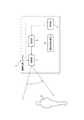
図1に示すように、本実施形態に係る電磁波検出装置10を含む情報取得システム11は、電磁波検出装置10、放射部12、走査部13、及び制御部14を含んで構成される。 As shown in FIG. 1, the
以降の図において、各機能ブロックを結ぶ破線は、制御信号または通信される情報の流れを示す。破線が示す通信は有線通信であってもよいし、無線通信であってもよい。また、各機能ブロックから突出する実線は、ビーム状の電磁波を示す。 In the following figures, the broken line connecting the functional blocks indicates the flow of control signals or information to be communicated. The communication indicated by the broken line may be wired communication or wireless communication. The solid line protruding from each functional block indicates a beam-shaped electromagnetic wave.
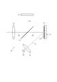
図2に示すように、電磁波検出装置10は、前段光学系15、分離部16、検出部17、進行部18、後段光学系19、及び検出部20を有する。ここにおいて、検出部17及び20は、それぞれ、「第1の検出部」及び「第2の検出部」に対応する。 As shown in FIG. 2, the electromagnetic
前段光学系15は、例えば、レンズ及びミラーの少なくとも一方を含み、被写体となる対象obの像を結像させる。 The pre-stage
分離部16は、前段光学系15と、前段光学系15から所定の距離をおいて離れた対象obの像の、前段光学系15による結像位置である一次結像位置との間に設けられる。 The
分離部16は、方向d0に沿って入射する電磁波を分離して、方向d1及び方向d2に進行するように分離する。入射の方向d0は、例えば、前段光学系15の光軸に平行であってよい。分離部16は、入射の方向d0に沿って進行する電磁波の一部を方向d1に進行させ、電磁波の別の一部を方向d2に進行させてよい。方向d1に進行させる一部の電磁波は、方向d0に沿って進行する電磁波のうち特定の波長の電磁波であってよく、方向d2に進行させる電磁波は他の波長の電磁波であってよい。 The
例えば、分離部16は、具体的には、可視光帯域の電磁波を方向d1に進行させ、赤外帯域の電磁波を方向d2に進行させてよい。反対に、分離部16は、赤外帯域の電磁波を方向d1に進行させ、可視光帯域の電磁波を方向d2に進行させてよい。また、分離部16は、長波長の電磁波を方向d1に進行させ、短波長の電磁波を方向d2に進行させてよい。反対に、分離部16は、長波長の電磁波を方向d1に進行させ、短波長の電磁波を方向d2に進行させてよい。 For example, the separating
本実施形態では、分離部16は、方向d0に進行する電磁波の一部を方向d1に反射し、電磁波の別の一部を方向d2に透過する。分離部16は、方向d0に進行する電磁波の一部を方向d1に透過し、電磁波の別の一部を方向d2に透過してもよい。また、分離部16は、方向d0に進行する電磁波の一部を方向d1に屈折させ、電磁波の別の一部を方向d2に屈折させてもよい。分離部16は、例えば、プリズムに蒸着された可視光反射コーティング、ハーフミラー、ビームスプリッタ、ダイクロイックミラー、コールドミラー、ホットミラー、メタサーフェス、及び偏向素子のいずれかを含む。 In the present embodiment, the
検出部17は、分離部16から方向d1に進行する電磁波の経路上に、設けられる。さらに、検出部17は、前段光学系15から所定の距離をおいて離れた対象obの像の、分離部16から方向d1における前段光学系15による結像位置または当該結像位置近傍に、設けられる。検出部17は、分離部16から方向d1に進行した電磁波を検出(または、電磁波の到来方向に存在する物体を示す信号を生成)する。 The detection unit 17 is provided on the path of the electromagnetic wave traveling from the
本実施形態において、検出部17は、例えばパッシブセンサであり、さらに具体的には、素子アレイを含む。検出部17は、例えば、イメージセンサまたはイメージングアレイなどの撮像素子を含み、検出面において結像した電磁波による像を撮像して、撮像した対象obに相当する画像情報を生成する。 In the present embodiment, the detection unit 17 is, for example, a passive sensor, and more specifically includes an element array. The detection unit 17 includes, for example, an image sensor such as an image sensor or an imaging array, captures an image of an electromagnetic wave formed on the detection surface, and generates image information corresponding to the captured object ob.
なお、本実施形態において、検出部17は、さらに具体的には可視光の像を撮像する。検出部17は、生成した画像情報を画像信号として制御部14に送信する。画像信号は、例えば、フレームごとに生成される。各フレームは、二次元に配列された画素信号からなる。例えば、1フレームは、一列数百〜数万個、一行数百〜数万個の画素からなる。例えば、1フレームの画素数は、1920×1080である。検出部17は、例えば、0.01秒〜0.04秒ごとに1フレームの画像信号を生成して制御部14に送信する。 In addition, in the present embodiment, the detection unit 17 more specifically captures an image of visible light. The detection unit 17 transmits the generated image information to the
なお、検出部17は、赤外線、紫外線、及び電波の像など、可視光以外の像を撮像して、それぞれの画像情報を生成してもよい。また、検出部17は測距センサを含んでもよい。この構成において、電磁波検出装置10は、検出部17により画像状の距離情報を取得し得る。また、検出部17はサーモセンサなどを含んでもよい。この構成において、電磁波検出装置10は、検出部17により画像状の温度情報を取得し得る。 The detection unit 17 may capture an image other than visible light, such as an image of infrared rays, ultraviolet rays, and radio waves, and generate respective image information. Further, the detection unit 17 may include a distance measuring sensor. With this configuration, the electromagnetic
進行部18は、分離部16から方向d2に進行する電磁波の経路上に設けられる。さらに、進行部18は、前段光学系15から所定の距離をおいて離れた対象obの像の、分離部16から方向d2における前段光学系15による一次結像位置または当該一次結像位置近傍に、設けられる。 The traveling
本実施形態においては、進行部18は、当該結像位置に設けられる。進行部18は、前段光学系15及び分離部16を通過した電磁波が入射する基準面ssを有する。基準面ssは、二次元状に配置される複数の画素pxによって構成される。基準面ssは、電磁波に、例えば、反射及び透過などの作用を生じさせる。 In the present embodiment, the advancing
進行部18は、方向d2に進行して基準面ssに入射する電磁波を、別の方向d3に進行させる。進行部18は、画素px毎に電磁波を反射する反射面を有する。進行部18は、画素px毎の反射面の向きを変更することにより、方向d2に進行して基準面ssに入射する電磁波の進行方向を、画素px毎に、方向d3またはさらに別の方向に切り替えることができる。 The traveling
本実施形態において、進行部18は、例えばDMD(Digital Micro mirror Device:デジタルマイクロミラーデバイス)を含む。DMDは、基準面ssを構成する微小な反射面を駆動することにより、画素px毎に当該反射面を基準面ssに対して、例えば+12°及び12°のいずれかの傾斜状態に切替え可能である。なお、基準面ssは、DMDにおける微小な反射面を載置する基板の板面に平行である。 In the present embodiment, the advancing
進行部18は、後述する制御部14の制御に基づいて、基準面ssに入射する電磁波の進行方向を、画素px毎に切り替える。 The advancing
後段光学系19は、進行部18から方向d3に設けられる。後段光学系19は、例えば、レンズ及びミラーの少なくとも一方を含む。後段光学系19は、進行部18において進行方向を切替えられた電磁波に対応する対象obの像を結像させる。 The rear
検出部20は、進行部18によって方向d3に進行した後に後段光学系19を経由して進行する電磁波の経路上に設けられる。検出部20は、後段光学系19を経由した電磁波を検出(または、電磁波の到来方向に存在する物体を示す信号を生成)する。 The
本実施形態において、検出部20は、放射部12から対象obに向けて放射された電磁波の当該対象obからの反射波を検出するアクティブセンサである。検出部20は、放射部12から放射され且つ走査部13により反射されることにより対象obに向けて放射された電磁波の当該対象obからの反射波を検出する。放射部12から放射される電磁波は赤外線、可視光線、紫外線、及び電波の少なくともいずれかであり、検出部20は、検出部17とは異種または同種の電磁波を検出する。 In the present embodiment, the
本実施形態において、検出部20は、検出部17と異種または同種のセンサであってよい。検出部20は、例えば、シリコン半導体に電場勾配をかけることで増幅機能を持たせた半導体素子である。かかる半導体素子は、測距センサを構成する素子、例えば、APD(Avalanche PhotoDiode)、MPPC(Multi−Pixel Photon Counter)、SPAD(Single Photon Avalanche Diode)、及び測距イメージセンサなどの素子を含む。また、検出部20は、APDアレイ、PDアレイ、測距イメージングアレイ、及び測距イメージセンサなどの素子アレイを含むものであってもよい。 In the present embodiment, the
本実施形態において、検出部20は、被写体からの反射波を検出したことを示す、増幅された検出信号を制御部14に送信する。検出部20は、例えば、0.1秒ごとに、フレーム単位の画像信号として、または他の形態の信号として、増幅された検出信号を制御部14に送信する。検出部20がフレーム単位の画素信号を生成する場合、例えば、1フレームは、一列1〜数百個、一行1〜数百個の画素からなる。検出部20は、さらに具体的には、赤外線の帯域の電磁波を検出する。 In the present embodiment, the
なお、検出部20は、上述した測距センサを構成する単一の素子である構成において、電磁波を検出できればよく、検出面において電磁波が結像しなくてもよい。それゆえ、検出部20は、後段光学系19による結像位置である二次結像位置に設けられなくてもよい。すなわち、検出部20は、すべての画角からの電磁波が検出面上に入射可能な位置であれば、進行部18により方向d3に進行した後に後段光学系19を経由して進行する電磁波の経路上のどこに配置されてもよい。 It should be noted that the
ここで図1を参照し、電磁波検出装置10を含む情報取得システム11の、電磁波検出装置10以外の各部の構成及び動作について説明する。放射部12は、赤外線、可視光線、紫外線、及び電波の少なくともいずれかを放射する。本実施形態において、放射部12は、赤外線を放射する。放射部12は、放射する電磁波を、対象obに向けて、直接または走査部13を介して間接的に、放射する。本実施形態においては、放射部12は、放射する電磁波を、対象obに向けて、走査部13を介して間接的に放射する。 Here, the configuration and operation of each unit other than the electromagnetic
放射部12は、幅の細い、例えば0.5°のビーム状の電磁波を放射する。また、本実施形態において、放射部12は電磁波をパルス状に放射可能である。例えば、放射部12は、LED(Light Emitting Diode)及びLD(Laser Diode)などを含む。放射部12は、制御部14の制御に基づいて、電磁波の放射及び停止を切り替える。 The radiating
走査部13は、例えば、電磁波を反射する反射面を有し、放射部12から放射された電磁波を、反射面の向きを変更しながら反射することにより、対象obに照射される電磁波の放射位置を変更する。すなわち、走査部13は、放射部12から放射される電磁波を用いて、対象obを走査する。よって、本実施形態において、検出部20は、走査部13と協働して、走査型の測距センサを構成する。なお、走査部13は、一次元方向または二次元方向に対象obを走査する。本実施形態においては、走査部13は、二次元方向に対象obを走査する。 The
走査部13は、放射部12から放射されて反射した電磁波の照射領域の少なくとも一部が、電磁波検出装置10における電磁波の検出範囲に含まれるように、構成される。よって、走査部13を介して対象obに照射される電磁波の少なくとも一部は、電磁波検出装置10において検出され得る。 The
なお、本実施形態において、走査部13は、放射部12から放射され且つ走査部13に反射した電磁波の放射領域の少なくとも一部が、検出部20における検出範囲に含まれるように、構成される。よって、本実施形態において、走査部13を介して対象obに放射される電磁波の少なくとも一部は、検出部20により検出され得る。 In the present embodiment, the
走査部13は、例えば、MEMS(Micro Electro Mechanical Systems)ミラー、ポリゴンミラー、及びガルバノミラーなどを含む。本実施形態においては、走査部13は、MEMSミラーを含む。 The
走査部13は、後述する制御部14の制御に基づいて、電磁波を反射する向きを変える。また、走査部13は、例えばエンコーダなどの角度センサを有してもよく、角度センサが検出する角度を、電磁波を反射する方向情報として、制御部14に通知してもよい。このような構成において、制御部14は、走査部13から取得する方向情報に基づいて、放射位置を算出し得る。また、制御部14は、走査部13に電磁波を反射する向きを変えさせるために入力する駆動信号に基づいて放射位置を算出し得る。 The
制御部14は、1以上のプロセッサ及びメモリを含む。プロセッサは、特定のプログラムを読み込ませて特定の機能を実行する汎用のプロセッサ、及び特定の処理に特化した専用のプロセッサの少なくともいずれかを含んでよい。専用のプロセッサは、特定用途向けIC(ASIC:Application Specific Integrated Circuit)を含んでよい。プロセッサは、プログラマブルロジックデバイス(PLD:Programmable Logic Device)を含んでよい。PLDは、FPGA(Field−Programmable Gate Array)を含んでよい。制御部14は、1つまたは複数のプロセッサが協働するSoC(System−on−a−Chip)、及びSiP(System In a Package)の少なくともいずれかを含んでもよい。 The
制御部14は、検出部17及び検出部20からそれぞれ送信される検出信号に基づいて、電磁波検出装置10の周囲に関する情報を取得する。周囲に関する情報は、例えば画像情報、距離情報、及び温度情報等である。本実施形態において、制御部14は、前述のように、検出部17が画像として検出した電磁波を画像情報として取得する。また、制御部14は、検出部20が検出する検出情報に基づいて、例えば、ToF(Time−of−Flight)方式により、放射部12に照射される照射位置の距離情報を取得する。 The
制御部14は、放射部12に電磁波放射信号を入力することにより、放射部12にパルス状の電磁波を放射させる。放射部12は、入力された当該電磁波放射信号に基づいて電磁波を放射する。放射部12が放射し且つ走査部13が反射して任意の放射領域に放射された電磁波は、当該放射領域において反射する。検出部20は、当該放射領域の反射波の進行部18における結像領域の中の少なくとも一部の画素pxの向きを切り替え、反射された電磁波を検出するとき、検出信号を制御部14に通知する。制御部14は、例えば、時間計測LSI(Large Scale Integrated circuit)を有しており、放射部12に電磁波を放射させてから検出信号を取得するまでの経過時間を計測する。制御部14は、当該経過時間に、光速を乗算し、且つ2で除算することにより、放射位置までの距離を算出する。なお、制御部14は、上述のように、走査部13から取得する方向情報、または自身が走査部13に出力する駆動信号に基づいて、放射位置を算出する。制御部14は、放射位置を変えながら、各放射位置までの距離を算出することにより、画像状の距離情報を作成する。 The
さらに、本実施形態において、制御部14は、検出部17の検出信号に基づいて検出部20の検出信号の増幅率を制御する。詳細は後述する。 Further, in the present embodiment, the
なお、情報取得システム11は、レーザ光を放射して、返ってくるまでの時間を直接測定するDirect ToFにより距離情報を作成する構成に限られず、例えば、電磁波を一定の周期で放射し、放射された電磁波と返ってきた電磁波との位相差から、返ってくるまでの時間を間接的に測定するFlash ToFにより距離情報を作成してもよい。また、情報取得システム11は、他のToF方式、例えば、Phased ToFにより距離情報を作成してもよい。 In addition, the
本実施形態において、検出部20は、電場勾配をかけることで検出信号を増幅する増幅機能を有する。かかる増幅機能の増幅率は、電場の強さに応じて増大する。しかし、増幅率を増大すべく電場を強くすると、増幅過程においてショットノイズが加わる。よって、電場を強くして増幅率を大きくすると、検出信号の利得も増大するが、それとともにノイズも大きくなるため、S/N比は必ずしも向上しない。また、かかるショットノイズは、検出部20に入力される電磁波の強度(つまり電磁波の強度に応じた入力電流)に応じて増加する。さらに、検出部20がAPDを有する場合、APDは温度に起因する熱雑音を有する。そして、熱雑音は、ショットノイズとは異なり、増幅率及び入力電流に依存しない。このように、検出部20では、検出信号の増幅に伴うショットノイズと、APD由来の熱雑音とを合わせた合成ノイズを有する。 In this embodiment, the
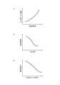
図3には、合成ノイズの増幅率依存性が示される。図3は、横軸に増幅率、縦軸に出力信号の強度を示す。まず、入力電流Iにおいて、増幅率の増加に伴う出力信号強度の直線的な増加が示される。また、ショットノイズsNは、増幅率の増加に伴って出力信号に混入したときの強度が指数関数的に増加する。一方、熱雑音hNは増幅率にかかわらず一定である。ここにおいて、ショットノイズsNと熱雑音hNとを合わせた合成ノイズmNの大きさは、増幅率に概ね依存することが示される。 FIG. 3 shows the amplification factor dependency of the synthetic noise. In FIG. 3, the horizontal axis represents the amplification factor and the vertical axis represents the intensity of the output signal. First, at the input current I, a linear increase in the output signal strength with an increase in the amplification factor is shown. In addition, the shot noise sN has an exponentially increased intensity when mixed with the output signal as the amplification factor increases. On the other hand, the thermal noise hN is constant regardless of the amplification factor. Here, it is shown that the magnitude of the combined noise mN, which is a combination of the shot noise sN and the thermal noise hN, depends substantially on the amplification factor.
また、図3に示すように、入力電流Iと合成ノイズmNとの乖離の大きさが、増幅率に応じたS/N比に対応する。ここでは、増幅率の増加に応じたS/N比SN_1、SN_2、SN_3が示される。ここにおいて、増幅率OpのときのS/N比SN_2が他より大きく、最良のS/N比である。このように、増幅率が大きければ、または小さければ、良好なS/N比が得られるとは限らない。以下、入力電流において最良のS/N比が得られる増幅率を最適増幅率(Op)という。 Further, as shown in FIG. 3, the magnitude of the deviation between the input current I and the combined noise mN corresponds to the S / N ratio according to the amplification factor. Here, the S / N ratios SN_1, SN_2, and SN_3 corresponding to the increase of the amplification factor are shown. Here, the S / N ratio SN_2 at the amplification rate Op is larger than the others, which is the best S / N ratio. Thus, if the amplification factor is large or small, a good S / N ratio is not always obtained. Hereinafter, the amplification factor that gives the best S / N ratio at the input current is called the optimum amplification factor (Op).
図4には、合成ノイズの入力電流依存性が示される。図4は、横軸に増幅率、縦軸に出力信号の強度を示す。ここでは、入力電流I1及び入力電流I1より小さい入力電流I2が示される。ここにおいて、入力電力I1のときの合成ノイズmN1と比較して、入力電力I2のときの合成ノイズmN2は、合成ノイズmN1と同等かそれより小さいことが示される。つまり、合成ノイズの大きさは、入力電流の大きさに概ね依存する。 FIG. 4 shows the input current dependency of the synthetic noise. In FIG. 4, the horizontal axis represents the amplification factor and the vertical axis represents the intensity of the output signal. Here, the input current I1 and the input current I2 smaller than the input current I1 are shown. Here, it is shown that the synthetic noise mN2 at the input power I2 is equal to or smaller than the synthetic noise mN1 as compared with the synthetic noise mN1 at the input power I1. That is, the magnitude of the combined noise depends substantially on the magnitude of the input current.
また、図4に示すように、入力電力I1のとき、合成ノイズmN1に対し、最適増幅率Op1のとき最良のS/N比SN_I1が得られる。一方、入力電力I2のとき、合成ノイズmN2に対し、最適増幅率Op2のとき最良のS/N比SN_I2が得られる。ここにおいて、入力電流I1のときの最適増幅率Op1より、入力電流I2のときの最適増幅率Op2の方が大きいことが示される。つまり、最適増幅率は入力電流に応じて異なり、入力電流が大きくなると、最適増幅率は小さくなる傾向がある。 Further, as shown in FIG. 4, at the input power I1, the best S / N ratio SN_I1 is obtained for the combined noise mN1 at the optimum amplification factor Op1. On the other hand, when the input power is I2, the best S / N ratio SN_I2 is obtained for the combined noise mN2 when the optimum amplification factor Op2 is obtained. Here, it is shown that the optimum gain Op2 at the input current I2 is larger than the optimum gain Op1 at the input current I1. That is, the optimum amplification factor differs depending on the input current, and when the input current increases, the optimum amplification factor tends to decrease.
本実施形態では、検出部20がAPD由来の合成ノイズを有することに鑑み、入力電流に応じて異なる最適増幅率で検出部20が検出信号を増幅するように検出部20を制御する。そうすることで、良好なS/N比の検出信号を得ることができる。 In the present embodiment, in view of the fact that the
具体的には、制御部14は、まず、検出部17の検出信号を取得する。検出部17は、検出部20より高い頻度で電磁波を検出する。そして、検出部17は、検出する電磁波の強度に応じた強度の検出信号を出力する。次いで検出部20が電磁波を検出するときに、制御部14は、検出部17の制御信号に基づいて検出部20の検出信号の増幅率を制御する。ここにおいて、検出部17と検出部20は同じ電磁波から分離された電磁波をそれぞれ検出するので、検出部17の検出信号の強度と検出部20の検出信号の強度は同等か、少なくとも相関する。たとえば、分離部16がダイクロックミラーである場合、波長以外の条件が同じ電磁波(光)がそれぞれ検出部17及び20で検出される。よって、検出部17の検出信号の強度に基づいて、検出部20が検出する電磁波の強度、すなわち入力電流の大きさを推定することができる。例えば、検出部17の検出信号の強度に基づいて検出部20が検出する電磁波の強度を推定する上で好適な例では、検出部17が検出する電磁波の波長帯域と検出部20が検出する電磁波の波長帯域の差が20000nm以下である。ここで、波長帯域の差は、波長帯域の上限値同士、下限値同士、中央値同士、最高感度波長同士、または最頻発波長同士の差であってよい。 Specifically, the
このことから、制御部14は、検出部17の検出信号の強度に基づいて、検出部20が検出する電磁波の強度、すなわち入力電流の大きさに対応する最適増幅率を検出部20に設定する。例えば、検出部17の検出信号が、電磁波の強度が比較的高いことを示すときには比較的低い最適増幅率が、電磁波の強度が比較的低いことを示すときには比較的高い最適増幅率が、検出部20に設定される。これにより、検出部20から良好なS/N比の検出信号が出力される。 From this, the
<実施例>
図5〜図8を用いて、一実施例における制御部14の動作を説明する。この実施例では、検出部17は、対象obを撮像するイメージセンサであり、検出部20は、対象obまでの距離を測定する測距センサである。例えば、情報取得システム11は、対象obを撮像するとともに対象obまでの距離を測定し、撮像画像と距離情報とを取得する。<Example>
The operation of the
図5の上段には、検出部17の電磁波検出(撮像)周期C17_n(nは整数)が模式的に示され、下段には検出部20の電磁波検出(測距)周期C20_nが模式的に示される。検出部17は、各周期C17_nで1フレームの画像の撮像を行う。一方、検出部20は、各周期C20_nで電磁波から1フレームごとの画像状の距離情報を検出する。ここにおいて、検出部17の電磁波検出頻度(フレームレート)は、検出部20の電磁波検出頻度(フレームレート)より高いことが示される。 The electromagnetic wave detection (imaging) cycle C17_n (n is an integer) of the detection unit 17 is schematically shown in the upper stage of FIG. 5, and the electromagnetic wave detection (distance measurement) cycle C20_n of the
制御部14は、まず、検出部17の周期C17_1における検出結果、つまり撮像画像の輝度情報を取得する(図6:ステップS10)。そして、制御部14は、検出部17の検出結果に基づいて、検出部20の最適増幅率を導出する(図6:ステップS20)。 The
制御部14は、図7に示されるような、検出部17及び20に入射する電磁波の強度、検出部20において電磁波強度に応じてAPDに入力される入力電流、及び検出部20における最適増幅率の関係に基づいて、検出部20の増幅率を制御する。すなわち、図7(A)に示されるように、電磁波強度に応じて検出部17の出力信号の強度(つまり検出部20における入力電流)は増加する。また、図7(B)に示されるように、検出部20における入力電流に応じて最適増幅率は減少する。そして、図7(A)及び図7(B)から、図7(C)に示されるような、検出部17からの出力信号の強度に応じて減少する検出部20の最適増幅率の関係を得ることができる。 As shown in FIG. 7, the
具体的には、制御部14は、図7(C)に示される検出部17からの出力信号と検出部20の最適増幅率との関係を、予め、内部メモリに記憶する。または、図8に示すように、制御部14は、検出部17からの出力信号(E1、E2、E3、…)に対応する検出部20の最適増幅率(Op1、Op2、Op3、…)を対応付けたテーブルデータを予め内部メモリに記憶する。そして、制御部14は、関係式またはテーブルを用いて、検出部17からの出力信号に基づいて、そのときの電磁波強度に適した検出部20の最適増幅率を導出し、導出した最適増幅率を検出部20に設定する。例えば、制御部14は、検出部20のAPDに最適増幅率に応じた電圧を印加する。または、制御部14は、最適増幅率に応じた電圧を印加する指示信号を、検出部20のAPDの制御回路に送ってもよい。そうすることで、検出部20の出力信号が最適増幅率で増幅され、良好なS/N比を得ることができる。 Specifically, the
図5、図6に戻ると、制御部14は、周期C17_1より後に到来する検出部20の周期C20_1で、検出部20に最適増幅率を設定する(図6:ステップS30)。なお、周期C17_1の終期と周期C20_1の始期の間の時間間隔は、制御部14、検出部17、20の処理速度の関係に応じて、任意に設定することができる。フレームレートの高い検出部17での検出結果を用いてフレームレートの低い検出部20の増幅率を制御することで、制御部14、検出部17、20の処理速度に応じて、検出部20の各フレームに対する増幅率制御に好適なタイミングで検出部17の検出結果を用いることができる。よって、たとえば、検出部20自らの過去の周期における検出結果に基づいて最適増幅率を設定しようとするより、フレームレートの高い検出部17の検出結果を用いることで、より新鮮な検出結果に基づいて即時性の高い制御が可能になる。 Returning to FIG. 5 and FIG. 6, the
以降、同様に、制御部14は、検出部17が周期C17_2で撮像した画像の輝度情報に基づいて、検出部20の周期C20_2で検出部20に最適増幅率を設定する。また、制御部14は、検出部17が周期C17_3で撮像した画像の輝度情報に基づいて、検出部20の周期C20_3で検出部20に最適増幅率を設定する。このように検出部20の毎フレームで増幅率を制御してもよいし、または、制御部14、検出部17、20の処理速度に応じて、検出部20の間欠的なフレームで増幅率を制御してもよい。 Thereafter, similarly, the
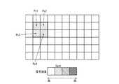
本実施例では、制御部14は、検出部17の1フレーム内の画素信号毎に、各画素信号の強度に基づいて、その画素信号に対応する検出部20の1フレーム内の画素信号の最適増幅率を、検出部20に設定する。ここで、検出部17の1フレーム内の画素信号と、これに対応する検出部20の1フレーム内の画素信号は、同じ方向から到来する電磁波を検出部17と検出部20がそれぞれ検出することによって得られる。 In this embodiment, the
図9A、9Bは、検出部17と検出部20が同じ解像度のフレームを検出する例を示す。図9Aには検出部17の1フレームF17に含まれる画素信号がマス目によって模式的に示され、各画素信号の4段階の強度がハッチングの密度により模式的に示される。また、図9Bには、図9AのフレームF17に対応する検出部20の1フレームF20が示される。ここでは、フレームF20に含まれる画素信号がマス目によって模式的に示され、各画素信号の4段階の最適増幅率がハッチングの密度によって模式的に示される。説明の便宜上、フレームF17、F20の画素信号Px1、Px2、Px3及びPx4についてのみ図示する。制御部14は、例えば、検出部17のフレームF17に含まれる画素信号Px1の強度Sg4に基づいて、検出部20のフレームF20における対応する画素信号Px1の最適増幅率Op_4を、検出部20に設定する。同様にして、フレームF17に含まれる画素信号Px2の強度Sg3に基づいて、フレームF20における対応する画素信号Px2の最適増幅率Op_3が、検出部20に設定される。また、フレームF17に含まれる画素信号Px3の強度Sg2に基づいて、フレームF20における対応する画素信号Px3の最適増幅率Op_2が、検出部20に設定される。そして、フレームF17に含まれる画素信号Px4の信号強度Sg1に基づいて、フレームF20における対応する画素信号Px4の最適増幅率Op_1が、検出部20に設定される。このように、画素信号ごとに最適増幅率を設定することで、検出部20の出力信号において精細な増幅率の制御ができ、良好なS/N比を得ることができる。 9A and 9B show an example in which the detection unit 17 and the
<変形例>
変形例では、制御部14は、検出部17の1フレーム内の画素信号群毎に、画素信号群の強度の平均を導出する。そして、その平均に対応する最適増幅率を、対応する検出部20の1フレーム内の画素信号群に対し設定してもよい。図10A、10B、11A、11B、12A、及び12Bには、それぞれ図9A、9Bと同様の表現で、検出部17の1フレームF17の画素信号、またはこれに対応する検出部20の1フレームF20の画素信号が示される。<Modification>
In the modification, the
制御部14は、例えば、図10Aに示す検出部17のフレームF17で、画素信号Px1、Px2、Px3、及びPx4からなる画素信号群において、画素信号Px1、Px2、Px3、及びPx4のそれぞれの強度Sg4、Sg3、Sg2、Sg1の平均Sgavを導出する。そして、制御部14は、図10Bに示す検出部20のフレームF20で、対応する画素信号群Px1、Px2、Px3、及びPx4に対し、平均Sgavに対応する最適増幅率Op_avを設定する。また、制御部14は、例えば図11Aに示すように、フレームF17に含まれる全画素信号の平均Avを導出し、図11Bに示すように、平均Avに対応する最適増幅率Op_avを、フレームF20に含まれる全画素信号に設定してもよい。The
また、例えば、図12Aに示すように、制御部14は、検出部17の1フレームF17に含まれる画素信号を領域Ar1〜Ar4に分割し、領域毎に画素信号の強度の平均を導出する。そして、図12Bに示すように、制御部14は、平均強度Av1〜Av4に対応する最適増幅率Op_av1〜Op_av4を、フレームF20の対応する領域Ar1〜Ar3に設定してもよい。ここでは、1フレームを4つの領域に分割する例を示したが、フレームを分割する領域の数はここに示したものに限られず、任意の数とすることが可能である。このように、画素信号群ごとに最適増幅率を設定することで、画素信号毎に最適増幅率を設定する場合より、最適増幅率を導出する処理の負担を軽減することができる。 Further, for example, as shown in FIG. 12A, the
なお、制御部14は、検出部20の1フレーム分の検出信号を取得・増幅しながらその一部に対し最適増幅率を設定してもよいし、予め進行部18の任意の画素pxを制御することで1フレームのうち一部の検出信号のみを取得・増幅する際に最適増幅率を設定してもよい。 The
さらに、検出部17と検出部20が異なる解像度のフレームを検出する場合には、制御部14は次のように動作することができる。例えば、検出部17の1フレーム内の1つの画素信号に検出部20の1フレーム内の複数の画素信号が対応する場合には、制御部14は、検出部17の画素信号の強度に対応する最適増幅率を、対応する検出部20の複数の画素信号に対し設定する。また、検出部17の1フレーム内の複数の画素信号に検出部20の1フレーム内の1つの画素信号が対応する場合には、制御部14は、検出部17の複数の画素信号の強度の平均を求め、その平均に対応する最適増幅率を、対応する検出部20の1つの画素信号に対し設定する。このようにして、検出部17と検出部20が異なる解像度のフレームを検出する場合であっても、検出部20の出力信号が最適増幅率で増幅され、良好なS/N比を得ることができる。 Furthermore, when the detection unit 17 and the
本発明の実施形態を諸図面及び実施例に基づき説明してきたが、当業者であれば本開示に基づき種々の変形及び修正を行うことが容易であることに注意されたい。従って、これらの変形及び修正は本発明の範囲に含まれることに留意されたい。 Although the embodiments of the present invention have been described based on the drawings and the examples, it should be noted that those skilled in the art can easily make various variations and modifications based on the present disclosure. Therefore, it should be noted that these variations and modifications are included in the scope of the present invention.
例えば、放射部12、走査部13、及び制御部14が、電磁波検出装置10とともに情報取得システム11を構成するが、電磁波検出装置10は、これらの少なくとも1つを含んで構成されてよい。 For example, although the
また、進行部18は、基準面ssに入射する電磁波の進行方向を2方向に切替え可能であるが、2方向のいずれかへの切替えでなく、3以上の方向に切替可能であってよい。 Further, the advancing
また、情報取得システム11は、放射部12から放射されるビーム状の電磁波を走査部13に走査させることにより、検出部20を走査部13と協同させて走査型のアクティブセンサとして機能させる構成を有する。しかし、情報取得システム11は、このような構成に限られない。例えば、放射状の電磁波を放射可能な複数の放射源を有する放射部12において、放射時期をずらしながら各放射源から電磁波を放射させるフェイズドスキャン方式により、走査部13を有することなく、走査型のアクティブセンサとして機能させる構成でも、本実施形態及と類似の効果が得られる。また、例えば、情報取得システム11は、走査部13を有さず、放射部12から放射状の電磁波を放射させ、走査なしで情報を取得する構成でも、本実施形態と類似の効果が得られる。 In addition, the
また、上述において、情報取得システム11は、検出部17がパッシブセンサであり、検出部20がアクティブセンサである構成を有する。しかし、情報取得システム11は、このような構成に限られない。例えば、情報取得システム11において、検出部17及び検出部20が共にアクティブセンサである構成でも、パッシブセンサである構成でも本実施形態と類似の効果が得られる。検出部17及び検出部20が共にアクティブセンサである構成において、対象obに電磁波を放射する放射部12は異なっていても、同一であってもよい。さらに、異なる放射部12は、それぞれ異種または同種の電磁波を放射してよい。 In addition, in the above description, the
また、本実施形態の進行部18は、図13に示すように、基準面ssに入射する電磁波を透過させて検出部20へ進行させる透過状態であってもよい。進行部181は、さらに画素px毎に電磁波を、透過させる電磁波とは異なる方向に反射する反射面を有するシャッタを含んでいてもよい。このような構成の進行部181においては、制御部14による制御のもと、画素px毎のシャッタを開閉することにより、透過状態と反射状態を画素px毎に切替え得る。 Further, as shown in FIG. 13, the advancing
このような構成の進行部181として、例えば、開閉可能な複数のシャッタがアレイ状に配列されたMEMSシャッタを含む進行部が挙げられる。また、進行部181として、電磁波を反射する反射状態と電磁波を透過する透過状態とを液晶配向に応じて切替え可能な液晶シャッタを含む進行部が挙げられる。このような構成の進行部181においては、画素px毎の液晶配向を切替えることにより、透過状態と反射状態を画素px毎に切替え得る。 Examples of the advancing
10 電磁波検出装置
11 情報取得システム
12 放射部
13 走査部
14 制御部
15 前段光学系
16 分離部
17、20 検出部
18 進行部
19 後段光学系
ob 対象
px 画素
ss 基準面10 Electromagnetic
Claims (31)
Translated fromJapanese分離された第1の電磁波を第1の頻度で検出する第1の検出部と、
前記第1の電磁波と異なる方向へ分離された第2の電磁波を前記第1の頻度より低い第2の頻度で検出し、検出信号の増幅率を前記第1の検出部の検出結果に応じて変化させる第2の検出部と、
を有する電磁波検出装置。A separation unit that separates and advances incident electromagnetic waves in multiple directions,
A first detection unit that detects the separated first electromagnetic wave at a first frequency;
The second electromagnetic wave separated in a direction different from the first electromagnetic wave is detected at a second frequency lower than the first frequency, and the amplification factor of the detection signal is determined according to the detection result of the first detection unit. A second detector that is changed,
Electromagnetic wave detection device having a.
前記第2の検出部は、前回第2の電磁波を検出した後に前記第1の検出部により検出された前記第1の電磁波の検出結果に応じて、前記増幅率を変化させる、
電磁波検出装置。In claim 1,
The second detection unit changes the amplification factor according to a detection result of the first electromagnetic wave detected by the first detection unit after detecting the second electromagnetic wave last time,
Electromagnetic wave detection device.
前記第2の検出部は、検出信号の増幅率を前記第1の検出部の検出結果の一部に基づいて設定する、
電磁波検出装置。In claim 1 or 2,
The second detection unit sets the amplification factor of the detection signal based on a part of the detection result of the first detection unit,
Electromagnetic wave detection device.
前記第2の検出部は、検出信号の増幅率を前記第1の検出部の検出結果の平均に基づいて設定する、
電磁波検出装置。In any one of Claim 1 thru | or 3,
The second detection unit sets an amplification factor of a detection signal based on an average of detection results of the first detection unit,
Electromagnetic wave detection device.
前記第2の検出部の前記増幅率は、前記第1の検出部の検出結果に基づいて当該増幅率を決定する制御部により設定される、
電磁波検出装置。In any one of Claim 1 thru | or 4,
The amplification factor of the second detection unit is set by a control unit that determines the amplification factor based on a detection result of the first detection unit,
Electromagnetic wave detection device.
前記制御部は、前記第1の検出部にて出力される前記第1の電磁波の強度に応じた出力信号に基づき、前記第2の検出部の増幅率を設定する、
電磁波検出装置。In claim 5,
The control unit sets an amplification factor of the second detection unit based on an output signal corresponding to the intensity of the first electromagnetic wave output from the first detection unit,
Electromagnetic wave detection device.
前記第1の検出部は、測距センサ、イメージセンサ、及びサーモセンサの少なくともいずれかを含む
電磁波検出装置。In any one of Claim 1 thru | or 6,
The first detection unit is an electromagnetic wave detection device including at least one of a distance measurement sensor, an image sensor, and a thermo sensor.
前記第1の検出部及び前記第2の検出部は、異種または同種のセンサを含む、
電磁波検出装置。In any one of Claim 1 thru | or 7,
The first detection unit and the second detection unit include sensors of different types or the same type,
Electromagnetic wave detection device.
前記第1の検出部は、赤外線、可視光線、紫外線、及び電波の少なくともいずれかを検出する、
電磁波検出装置。In any one of Claim 1 thru | or 8,
The first detection unit detects at least one of infrared rays, visible rays, ultraviolet rays, and radio waves,
Electromagnetic wave detection device.
前記第1の検出部及び前記第2の検出部は、同種または異種の電磁波を検出する、
電磁波検出装置。In any one of Claim 1 thru | or 9,
The first detection unit and the second detection unit detect electromagnetic waves of the same type or different types,
Electromagnetic wave detection device.
前記第1の検出部及び前記第2の検出部は、APD(Avalanche PhotoDiode)、MPPC(Multi−Pixel Photon Counter)、SPAD(Single Photon Avalanche Diode)その他の半導体素子を含む、
電磁波検出装置。In any one of Claim 1 thru | or 10,
The first detection unit and the second detection unit include APD (Avalanche PhotoDiode), MPPC (Multi-Pixel Photon Counter), SPAD (Single Photon Avalanche Diode) and other semiconductor elements.
Electromagnetic wave detection device.
前記分離部は、入射する前記電磁波を波長に応じて複数の方向に分離して進行させる、
電磁波検出装置。In any one of Claim 1 thru | or 11,
The separation unit separates the incident electromagnetic wave into a plurality of directions according to the wavelength to proceed.
Electromagnetic wave detection device.
前記第1の電磁波と前記第2の電磁波の波長帯域の差は20000nm以下である、
電磁波検出装置。In claim 12,
The difference between the wavelength bands of the first electromagnetic wave and the second electromagnetic wave is 20000 nm or less,
Electromagnetic wave detection device.
前記第2の電磁波の進行方向を画素ごとに切換えて前記第2の検出部へ進行させる進行部をさらに有する、
電磁波検出装置。In any one of Claim 1 thru | or 13,
A traveling unit that switches the traveling direction of the second electromagnetic wave for each pixel and travels to the second detection unit.
Electromagnetic wave detection device.
前記進行部は、電磁波を反射する反射面を前記画素毎に有し、当該反射面の向きを前記画素毎に変更することにより前記第2の電磁波の進行方向を、前記第2の検出部に向かう方向および該方向以外の方向に切り替える、
電磁波検出装置。In claim 14,
The traveling unit has a reflecting surface that reflects electromagnetic waves for each of the pixels, and changes the direction of the reflecting surface for each of the pixels so that the traveling direction of the second electromagnetic wave is transmitted to the second detecting unit. Switching to the direction to go and the direction other than that,
Electromagnetic wave detection device.
前記進行部は、前記基準面に入射した電磁波を透過させて前記第2の検出部に進行させる透過する透過状態と、前記第2の検出部に向かう方向とは別の方向に反射させる反射状態を、前記画素毎に切替える、
電磁波検出装置。In Claim 14 or 15,
The advancing section transmits an electromagnetic wave that has entered the reference surface and transmits the electromagnetic wave to the second detecting section, and transmits the electromagnetic wave and a reflecting state that reflects the electromagnetic wave in a direction different from a direction toward the second detecting section. , For each pixel,
Electromagnetic wave detection device.
前記進行部は、電磁波を反射する反射面を含むシャッタを前記画素毎に含み、前記シャ
ッタを前記画素毎に開閉することにより前記反射状態と前記透過状態とに、切替える、
電磁波検出装置。In claim 16,
The traveling unit includes a shutter including a reflective surface that reflects electromagnetic waves for each pixel, and switches between the reflective state and the transmissive state by opening and closing the shutter for each pixel.
Electromagnetic wave detection device.
前記進行部は、前記シャッタがアレイ状に配列されたMEMSシャッタを含む、
電磁波検出装置。In claim 17,
The advancing unit includes a MEMS shutter in which the shutters are arranged in an array.
Electromagnetic wave detection device.
前記進行部は、電磁波を反射する反射状態および透過する透過状態を液晶配光に応じて
前記画素毎に切替え可能な液晶シャッタを含む、
電磁波検出装置。In Claim 16 or 17,
The traveling unit includes a liquid crystal shutter capable of switching between a reflective state in which electromagnetic waves are reflected and a transmissive state in which electromagnetic waves are transmitted, for each pixel according to liquid crystal light distribution,
Electromagnetic wave detection device.
前記進行部は、デジタルマイクロミラーデバイスを有する、
電磁波検出装置。In any one of Claim 15 thru | or 19,
The traveling unit has a digital micromirror device,
Electromagnetic wave detection device.
前記分離部は、可視光反射コーティング、ハーフミラー、ビームスプリッタ、ダイクロイックミラー、コールドミラー、ホットミラー、メタサーフェス、及び偏向素子の少なくともいずれかを含む、
電磁波検出装置。In any one of Claim 1 thru | or 20,
The separation unit includes at least one of a visible light reflective coating, a half mirror, a beam splitter, a dichroic mirror, a cold mirror, a hot mirror, a metasurface, and a deflection element,
Electromagnetic wave detection device.
前記第1の検出部及び前記第2の検出部はそれぞれ、放射部から対象に向けて放射された電磁波の前記対象からの反射波を検出するアクティブセンサ、またはパッシブセンサを含む、
電磁波検出装置。In any one of Claim 1 thru | or 21,
Each of the first detection unit and the second detection unit includes an active sensor that detects a reflected wave from the target of an electromagnetic wave emitted from the radiation unit toward the target, or a passive sensor.
Electromagnetic wave detection device.
前記第1の検出部及び前記第2の検出部はそれぞれ、異なる放射部、または同一の放射部から対象に向けて放射された電磁波の前記対象からの反射波を検出するアクティブセンサを含む、
電磁波検出装置。In any one of Claim 1 thru | or 22,
The first detection unit and the second detection unit each include an active sensor that detects a reflected wave from the target of an electromagnetic wave radiated toward the target from a different radiating unit or the same radiating unit,
Electromagnetic wave detection device.
前記異なる放射部はそれぞれ、異種または同種の電磁波を放射する、
電磁波検出装置。In Claim 23,
The different radiators emit different or same types of electromagnetic waves,
Electromagnetic wave detection device.
前記放射部は、赤外線、可視光線、紫外線、及び電波のいずれかを放射する、
電磁波検出装置。In any one of Claim 22 to 24,
The radiation unit emits any one of infrared rays, visible rays, ultraviolet rays, and radio waves,
Electromagnetic wave detection device.
前記放射部は、フェイズドスキャン方式により電磁波を走査する
電磁波検出装置。In any one of Claim 22 thru | or 25,
An electromagnetic wave detection device in which the radiation unit scans an electromagnetic wave by a phased scan method.
前記放射部から放射される電磁波を用いて走査する走査部を、さらに有する
電磁波検出装置。In any one of Claim 22 thru | or 25,
The electromagnetic wave detection device further comprising a scanning unit that scans using electromagnetic waves emitted from the emission unit.
前記走査部は、電磁波を反射する反射面を含み、前記放射部から放射される電磁波を、前記反射面の向きを変更しながら前記反射面に反射させることにより、走査する
電磁波検出装置。In claim 19,
An electromagnetic wave detection device, wherein the scanning unit includes a reflection surface that reflects electromagnetic waves, and scans the electromagnetic waves emitted from the radiation unit by reflecting the electromagnetic waves on the reflection surface while changing the direction of the reflection surface.
前記走査部は、MEMSミラー、ポリゴンミラー、ガルバノミラーのいずれかを含む、
電磁波検出装置。In Claim 19 or 28,
The scanning unit includes any one of a MEMS mirror, a polygon mirror, and a galvano mirror,
Electromagnetic wave detection device.
前記電磁波検出装置と、
前記第1の検出部及び前記第2の検出部による電磁波の検出結果に基づいて、周囲に関する情報を取得する制御部とを、有する
情報取得システム。In any one of Claims 1 to 29,
The electromagnetic wave detection device,
An information acquisition system, comprising: a control unit that acquires information about the surroundings based on detection results of electromagnetic waves by the first detection unit and the second detection unit.
前記制御部は、前記周囲に関する情報として、画像情報、距離情報、及び温度情報の少なくともいずれかを取得する、
情報取得システム。
In claim 30,
The control unit acquires at least one of image information, distance information, and temperature information as the information about the surroundings,
Information acquisition system.
Priority Applications (3)
| Application Number | Priority Date | Filing Date | Title |
|---|---|---|---|
| JP2018206478AJP6978394B2 (en) | 2018-11-01 | 2018-11-01 | Electromagnetic wave detection device and information acquisition system |
| US17/286,060US12270907B2 (en) | 2018-11-01 | 2019-10-21 | Electromagnetic wave detection apparatus and information acquisition system |
| PCT/JP2019/041391WO2020090558A1 (en) | 2018-11-01 | 2019-10-21 | Electromagnetic wave detecting device, and information acquiring system |
Applications Claiming Priority (1)
| Application Number | Priority Date | Filing Date | Title |
|---|---|---|---|
| JP2018206478AJP6978394B2 (en) | 2018-11-01 | 2018-11-01 | Electromagnetic wave detection device and information acquisition system |
Publications (3)
| Publication Number | Publication Date |
|---|---|
| JP2020071169Atrue JP2020071169A (en) | 2020-05-07 |
| JP2020071169A5 JP2020071169A5 (en) | 2021-02-18 |
| JP6978394B2 JP6978394B2 (en) | 2021-12-08 |
Family
ID=70463090
Family Applications (1)
| Application Number | Title | Priority Date | Filing Date |
|---|---|---|---|
| JP2018206478AActiveJP6978394B2 (en) | 2018-11-01 | 2018-11-01 | Electromagnetic wave detection device and information acquisition system |
Country Status (3)
| Country | Link |
|---|---|
| US (1) | US12270907B2 (en) |
| JP (1) | JP6978394B2 (en) |
| WO (1) | WO2020090558A1 (en) |
Citations (4)
| Publication number | Priority date | Publication date | Assignee | Title |
|---|---|---|---|---|
| JPS63233391A (en)* | 1987-03-20 | 1988-09-29 | Ricoh Co Ltd | Distance measurement method |
| JP2003028959A (en)* | 2001-07-17 | 2003-01-29 | Kawasaki Heavy Ind Ltd | Target extraction method |
| US20110317005A1 (en)* | 2009-03-12 | 2011-12-29 | Lee Warren Atkinson | Depth-Sensing Camera System |
| WO2017151660A1 (en)* | 2016-02-29 | 2017-09-08 | Tetravue, Inc. | 3d imaging system and method |
Family Cites Families (18)
| Publication number | Priority date | Publication date | Assignee | Title |
|---|---|---|---|---|
| US6380871B1 (en)* | 1999-11-30 | 2002-04-30 | Optical Systems, Inc. | System for and method of searching for targets in a marine environment |
| US7049597B2 (en)* | 2001-12-21 | 2006-05-23 | Andrew Bodkin | Multi-mode optical imager |
| JP2006201037A (en)* | 2005-01-20 | 2006-08-03 | Ricoh Co Ltd | Shape measuring device |
| US7375804B2 (en)* | 2005-03-01 | 2008-05-20 | Lockheed Martin Corporation | Single detector receiver for multi-beam LADAR systems |
| JP4738082B2 (en)* | 2005-07-22 | 2011-08-03 | 古野電気株式会社 | Gain control circuit |
| DE102009029376A1 (en)* | 2009-09-11 | 2011-05-12 | Robert Bosch Gmbh | Photon detector with paralyzable photon-sensitive element, in particular SPAD, as well as distance measuring device with such a photon detector |
| JP2011220732A (en) | 2010-04-06 | 2011-11-04 | Honda Motor Co Ltd | Vehicle surroundings monitoring device |
| US9098753B1 (en)* | 2014-04-25 | 2015-08-04 | Google Inc. | Methods and systems for object detection using multiple sensors |
| JP2017011634A (en)* | 2015-06-26 | 2017-01-12 | キヤノン株式会社 | Imaging device, control method for the same and program |
| EP3315937A4 (en)* | 2015-08-04 | 2018-07-11 | Konica Minolta, Inc. | Gas detection device and gas detection method |
| JP6849371B2 (en)* | 2015-10-08 | 2021-03-24 | 三星電子株式会社Samsung Electronics Co.,Ltd. | Side emission laser light source and 3D image acquisition device including it |
| US20170357000A1 (en)* | 2016-06-09 | 2017-12-14 | Texas Instruments Incorporated | Processing techniques for lidar receiver using spatial light modulators |
| JP6894268B2 (en)* | 2017-03-17 | 2021-06-30 | 京セラ株式会社 | Electromagnetic wave detectors, programs, and electromagnetic wave detection systems |
| CN211236238U (en)* | 2017-03-29 | 2020-08-11 | 深圳市大疆创新科技有限公司 | Light detection and ranging (LIDAR) system and unmanned vehicle |
| US20180284246A1 (en)* | 2017-03-31 | 2018-10-04 | Luminar Technologies, Inc. | Using Acoustic Signals to Modify Operation of a Lidar System |
| CN109588060B (en)* | 2017-07-28 | 2021-05-11 | 谷歌有限责任公司 | Method for controlling a sensor and corresponding device, vehicle, system and computer-readable storage medium |
| JP2019028013A (en)* | 2017-08-03 | 2019-02-21 | オムロンオートモーティブエレクトロニクス株式会社 | Object detection device |
| US11435752B2 (en)* | 2018-03-23 | 2022-09-06 | Motional Ad Llc | Data fusion system for a vehicle equipped with unsynchronized perception sensors |
- 2018
- 2018-11-01JPJP2018206478Apatent/JP6978394B2/enactiveActive
- 2019
- 2019-10-21USUS17/286,060patent/US12270907B2/enactiveActive
- 2019-10-21WOPCT/JP2019/041391patent/WO2020090558A1/ennot_activeCeased
Patent Citations (4)
| Publication number | Priority date | Publication date | Assignee | Title |
|---|---|---|---|---|
| JPS63233391A (en)* | 1987-03-20 | 1988-09-29 | Ricoh Co Ltd | Distance measurement method |
| JP2003028959A (en)* | 2001-07-17 | 2003-01-29 | Kawasaki Heavy Ind Ltd | Target extraction method |
| US20110317005A1 (en)* | 2009-03-12 | 2011-12-29 | Lee Warren Atkinson | Depth-Sensing Camera System |
| WO2017151660A1 (en)* | 2016-02-29 | 2017-09-08 | Tetravue, Inc. | 3d imaging system and method |
Also Published As
| Publication number | Publication date |
|---|---|
| US12270907B2 (en) | 2025-04-08 |
| JP6978394B2 (en) | 2021-12-08 |
| US20210364640A1 (en) | 2021-11-25 |
| WO2020090558A1 (en) | 2020-05-07 |
Similar Documents
| Publication | Publication Date | Title |
|---|---|---|
| JP7387803B2 (en) | Electromagnetic wave detection device and information acquisition system | |
| US11408982B2 (en) | Electromagnetic wave detection apparatus, program, and electromagnetic wave detection system | |
| US11675052B2 (en) | Electromagnetic wave detection apparatus, program, and electromagnetic wave detection system | |
| US12196890B2 (en) | Electromagnetic wave detection apparatus, program, and information acquisition system | |
| US11194021B2 (en) | Electromagnetic wave detection apparatus, program, and electromagnetic wave detection system comprising a controller to update related information associating an emission direction and two elements defining two points on a path of electromagnetic waves | |
| US11754678B2 (en) | Electromagnetic wave detection apparatus, program, and electromagnetic wave detection system | |
| US11573301B2 (en) | Electromagnetic wave detection apparatus, program, and electromagnetic wave detection system | |
| JP2019129510A (en) | Electromagnetic wave detection device and information acquisition system | |
| US20210341615A1 (en) | Method for adjusting electromagnetic wave detecting device, electromagnetic wave detecting device, and information acquiring system | |
| JP6978394B2 (en) | Electromagnetic wave detection device and information acquisition system | |
| CN116840816A (en) | Electromagnetic wave detection device and information acquisition system | |
| JP7037609B2 (en) | Electromagnetic wave detectors and programs | |
| JP2020067403A (en) | Electromagnetic wave detection device | |
| JP2020085538A (en) | Electromagnetic wave detection device and information acquisition system | |
| JP2020060396A (en) | Electromagnetic wave detection device and data acquisition system | |
| JP2020073894A (en) | Electromagnetic wave detection device and information acquisition system | |
| JP2020073895A (en) | Electromagnetic wave detection device and information acquisition system | |
| WO2020022150A1 (en) | Electromagnetic wave detection device and information acquisition system | |
| JP2020071168A (en) | Electromagnetic wave detection device and information acquisition system | |
| JP2019002847A (en) | Electromagnetic wave detector and information acquisition system | |
| JP2019200103A (en) | Electromagnetic wave detector and information acquisition system |
Legal Events
| Date | Code | Title | Description |
|---|---|---|---|
| A521 | Request for written amendment filed | Free format text:JAPANESE INTERMEDIATE CODE: A523 Effective date:20210104 | |
| A621 | Written request for application examination | Free format text:JAPANESE INTERMEDIATE CODE: A621 Effective date:20210112 | |
| A131 | Notification of reasons for refusal | Free format text:JAPANESE INTERMEDIATE CODE: A131 Effective date:20210810 | |
| A521 | Request for written amendment filed | Free format text:JAPANESE INTERMEDIATE CODE: A523 Effective date:20211007 | |
| TRDD | Decision of grant or rejection written | ||
| A01 | Written decision to grant a patent or to grant a registration (utility model) | Free format text:JAPANESE INTERMEDIATE CODE: A01 Effective date:20211026 | |
| A61 | First payment of annual fees (during grant procedure) | Free format text:JAPANESE INTERMEDIATE CODE: A61 Effective date:20211111 | |
| R150 | Certificate of patent or registration of utility model | Ref document number:6978394 Country of ref document:JP Free format text:JAPANESE INTERMEDIATE CODE: R150 |