JP2020042034A6 - Chemical sensor with consistent sensor surface area - Google Patents
Chemical sensor with consistent sensor surface areaDownload PDFInfo
- Publication number
- JP2020042034A6 JP2020042034A6JP2019199636AJP2019199636AJP2020042034A6JP 2020042034 A6JP2020042034 A6JP 2020042034A6JP 2019199636 AJP2019199636 AJP 2019199636AJP 2019199636 AJP2019199636 AJP 2019199636AJP 2020042034 A6JP2020042034 A6JP 2020042034A6
- Authority
- JP
- Japan
- Prior art keywords
- insulator
- opening
- conductive element
- chemical sensor
- floating gate
- Prior art date
- Legal status (The legal status is an assumption and is not a legal conclusion. Google has not performed a legal analysis and makes no representation as to the accuracy of the status listed.)
- Pending
Links
- 239000000126substanceSubstances0.000titleclaimsabstractdescription117
- 239000004020conductorSubstances0.000claimsabstractdescription92
- 239000012212insulatorSubstances0.000claimsabstractdescription92
- 238000007667floatingMethods0.000claimsabstractdescription38
- 238000004519manufacturing processMethods0.000claimsabstractdescription33
- 230000005669field effectEffects0.000claimsabstractdescription15
- 238000006243chemical reactionMethods0.000claimsdescription91
- 239000000463materialSubstances0.000claimsdescription87
- 238000000034methodMethods0.000claimsdescription51
- 229920002120photoresistant polymerPolymers0.000claimsdescription15
- 238000000151depositionMethods0.000claimsdescription9
- RTAQQCXQSZGOHL-UHFFFAOYSA-NTitaniumChemical compound[Ti]RTAQQCXQSZGOHL-UHFFFAOYSA-N0.000claimsdescription8
- 238000005530etchingMethods0.000claimsdescription8
- 229910052719titaniumInorganic materials0.000claimsdescription8
- 239000010936titaniumSubstances0.000claimsdescription8
- 230000004044responseEffects0.000claimsdescription5
- 238000010586diagramMethods0.000abstractdescription4
- 239000010410layerSubstances0.000description44
- 230000008569processEffects0.000description20
- 239000003153chemical reaction reagentSubstances0.000description18
- 150000002500ionsChemical class0.000description15
- VYPSYNLAJGMNEJ-UHFFFAOYSA-NSilicium dioxideChemical compoundO=[Si]=OVYPSYNLAJGMNEJ-UHFFFAOYSA-N0.000description14
- 239000012491analyteSubstances0.000description10
- 238000000231atomic layer depositionMethods0.000description10
- 239000012530fluidSubstances0.000description10
- 238000004518low pressure chemical vapour depositionMethods0.000description10
- 238000000623plasma-assisted chemical vapour depositionMethods0.000description10
- 238000003491arrayMethods0.000description9
- 150000007523nucleic acidsChemical group0.000description8
- 239000002773nucleotideSubstances0.000description7
- 125000003729nucleotide groupChemical group0.000description7
- 229910052581Si3N4Inorganic materials0.000description6
- NRTOMJZYCJJWKI-UHFFFAOYSA-NTitanium nitrideChemical compound[Ti]#NNRTOMJZYCJJWKI-UHFFFAOYSA-N0.000description6
- 229910052751metalInorganic materials0.000description6
- 239000002184metalSubstances0.000description6
- 235000012239silicon dioxideNutrition0.000description6
- 239000000377silicon dioxideSubstances0.000description6
- HQVNEWCFYHHQES-UHFFFAOYSA-Nsilicon nitrideChemical compoundN12[Si]34N5[Si]62N3[Si]51N64HQVNEWCFYHHQES-UHFFFAOYSA-N0.000description6
- 239000007787solidSubstances0.000description6
- 239000000758substrateSubstances0.000description6
- 239000006227byproductSubstances0.000description5
- 230000008859changeEffects0.000description5
- 238000005229chemical vapour depositionMethods0.000description5
- 238000012545processingMethods0.000description5
- 238000005546reactive sputteringMethods0.000description5
- 239000004065semiconductorSubstances0.000description5
- 239000011540sensing materialSubstances0.000description5
- 238000004544sputter depositionMethods0.000description5
- -1hydrogen ionsChemical class0.000description4
- 108020004707nucleic acidsProteins0.000description4
- 102000039446nucleic acidsHuman genes0.000description4
- 230000036961partial effectEffects0.000description4
- 238000001020plasma etchingMethods0.000description4
- 230000035945sensitivityEffects0.000description4
- 238000012163sequencing techniqueMethods0.000description4
- 238000012408PCR amplificationMethods0.000description3
- 238000004140cleaningMethods0.000description3
- 230000007423decreaseEffects0.000description3
- 239000001257hydrogenSubstances0.000description3
- 229910052739hydrogenInorganic materials0.000description3
- 230000002829reductive effectEffects0.000description3
- YCKRFDGAMUMZLT-UHFFFAOYSA-NFluorine atomChemical compound[F]YCKRFDGAMUMZLT-UHFFFAOYSA-N0.000description2
- XEEYBQQBJWHFJM-UHFFFAOYSA-NIronChemical compound[Fe]XEEYBQQBJWHFJM-UHFFFAOYSA-N0.000description2
- PXHVJJICTQNCMI-UHFFFAOYSA-NNickelChemical compound[Ni]PXHVJJICTQNCMI-UHFFFAOYSA-N0.000description2
- 108091028043Nucleic acid sequenceProteins0.000description2
- KDLHZDBZIXYQEI-UHFFFAOYSA-NPalladiumChemical compound[Pd]KDLHZDBZIXYQEI-UHFFFAOYSA-N0.000description2
- BQCADISMDOOEFD-UHFFFAOYSA-NSilverChemical compound[Ag]BQCADISMDOOEFD-UHFFFAOYSA-N0.000description2
- 229910052782aluminiumInorganic materials0.000description2
- XAGFODPZIPBFFR-UHFFFAOYSA-NaluminiumChemical compound[Al]XAGFODPZIPBFFR-UHFFFAOYSA-N0.000description2
- 230000003321amplificationEffects0.000description2
- 238000004458analytical methodMethods0.000description2
- 230000004888barrier functionEffects0.000description2
- 239000011324beadSubstances0.000description2
- 230000031018biological processes and functionsEffects0.000description2
- 229910010293ceramic materialInorganic materials0.000description2
- 238000004891communicationMethods0.000description2
- 230000001419dependent effectEffects0.000description2
- 230000008021depositionEffects0.000description2
- 238000001514detection methodMethods0.000description2
- 238000009792diffusion processMethods0.000description2
- 238000001312dry etchingMethods0.000description2
- 238000002474experimental methodMethods0.000description2
- 229910052731fluorineInorganic materials0.000description2
- 239000011737fluorineSubstances0.000description2
- 230000004907fluxEffects0.000description2
- 230000006870functionEffects0.000description2
- 238000010348incorporationMethods0.000description2
- 238000005468ion implantationMethods0.000description2
- 238000002372labellingMethods0.000description2
- 239000007769metal materialSubstances0.000description2
- 239000011859microparticleSubstances0.000description2
- 238000003541multi-stage reactionMethods0.000description2
- 238000003199nucleic acid amplification methodMethods0.000description2
- 239000002245particleSubstances0.000description2
- BASFCYQUMIYNBI-UHFFFAOYSA-NplatinumChemical compound[Pt]BASFCYQUMIYNBI-UHFFFAOYSA-N0.000description2
- 229910021420polycrystalline siliconInorganic materials0.000description2
- 229920005591polysiliconPolymers0.000description2
- 230000009467reductionEffects0.000description2
- 229910052814silicon oxideInorganic materials0.000description2
- 229910052709silverInorganic materials0.000description2
- 239000004332silverSubstances0.000description2
- WXAHAOIEHWDLLL-UHFFFAOYSA-Ntitanium hydrobromideChemical compound[Ti].BrWXAHAOIEHWDLLL-UHFFFAOYSA-N0.000description2
- WFKWXMTUELFFGS-UHFFFAOYSA-NtungstenChemical compound[W]WFKWXMTUELFFGS-UHFFFAOYSA-N0.000description2
- 229910052721tungstenInorganic materials0.000description2
- 239000010937tungstenSubstances0.000description2
- 239000002699waste materialSubstances0.000description2
- 108091093088AmpliconProteins0.000description1
- WKBOTKDWSSQWDR-UHFFFAOYSA-NBromine atomChemical compound[Br]WKBOTKDWSSQWDR-UHFFFAOYSA-N0.000description1
- OYPRJOBELJOOCE-UHFFFAOYSA-NCalciumChemical compound[Ca]OYPRJOBELJOOCE-UHFFFAOYSA-N0.000description1
- RYGMFSIKBFXOCR-UHFFFAOYSA-NCopperChemical compound[Cu]RYGMFSIKBFXOCR-UHFFFAOYSA-N0.000description1
- DGAQECJNVWCQMB-PUAWFVPOSA-MIlexoside XXIXChemical compoundC[C@@H]1CC[C@@]2(CC[C@@]3(C(=CC[C@H]4[C@]3(CC[C@@H]5[C@@]4(CC[C@@H](C5(C)C)OS(=O)(=O)[O-])C)C)[C@@H]2[C@]1(C)O)C)C(=O)O[C@H]6[C@@H]([C@H]([C@@H]([C@H](O6)CO)O)O)O.[Na+]DGAQECJNVWCQMB-PUAWFVPOSA-M0.000description1
- 102000018120RecombinasesHuman genes0.000description1
- 108010091086RecombinasesProteins0.000description1
- XUIMIQQOPSSXEZ-UHFFFAOYSA-NSiliconChemical compound[Si]XUIMIQQOPSSXEZ-UHFFFAOYSA-N0.000description1
- GWEVSGVZZGPLCZ-UHFFFAOYSA-NTitan oxideChemical compoundO=[Ti]=OGWEVSGVZZGPLCZ-UHFFFAOYSA-N0.000description1
- 108010067973ValinomycinProteins0.000description1
- QCWXUUIWCKQGHC-UHFFFAOYSA-NZirconiumChemical compound[Zr]QCWXUUIWCKQGHC-UHFFFAOYSA-N0.000description1
- 229910045601alloyInorganic materials0.000description1
- 239000000956alloySubstances0.000description1
- UQZIWOQVLUASCR-UHFFFAOYSA-Nalumane;titaniumChemical compound[AlH3].[Ti]UQZIWOQVLUASCR-UHFFFAOYSA-N0.000description1
- 230000008901benefitEffects0.000description1
- 230000015572biosynthetic processEffects0.000description1
- GDTBXPJZTBHREO-UHFFFAOYSA-NbromineSubstancesBrBrGDTBXPJZTBHREO-UHFFFAOYSA-N0.000description1
- 229910052794bromiumInorganic materials0.000description1
- 229910052791calciumInorganic materials0.000description1
- 239000011575calciumSubstances0.000description1
- 239000000919ceramicSubstances0.000description1
- 238000001311chemical methods and processMethods0.000description1
- FCFNRCROJUBPLU-UHFFFAOYSA-Ncompound M126Natural productsCC(C)C1NC(=O)C(C)OC(=O)C(C(C)C)NC(=O)C(C(C)C)OC(=O)C(C(C)C)NC(=O)C(C)OC(=O)C(C(C)C)NC(=O)C(C(C)C)OC(=O)C(C(C)C)NC(=O)C(C)OC(=O)C(C(C)C)NC(=O)C(C(C)C)OC1=OFCFNRCROJUBPLU-UHFFFAOYSA-N0.000description1
- 150000001875compoundsChemical class0.000description1
- 239000000470constituentSubstances0.000description1
- 229910052802copperInorganic materials0.000description1
- 239000010949copperSubstances0.000description1
- 230000005595deprotonationEffects0.000description1
- 238000010537deprotonation reactionMethods0.000description1
- 239000000839emulsionSubstances0.000description1
- 238000005516engineering processMethods0.000description1
- 239000012634fragmentSubstances0.000description1
- 239000007789gasSubstances0.000description1
- 239000000499gelSubstances0.000description1
- PCHJSUWPFVWCPO-UHFFFAOYSA-NgoldChemical compound[Au]PCHJSUWPFVWCPO-UHFFFAOYSA-N0.000description1
- 229910052737goldInorganic materials0.000description1
- 239000010931goldSubstances0.000description1
- 229910052735hafniumInorganic materials0.000description1
- VBJZVLUMGGDVMO-UHFFFAOYSA-Nhafnium atomChemical compound[Hf]VBJZVLUMGGDVMO-UHFFFAOYSA-N0.000description1
- 239000011810insulating materialSubstances0.000description1
- PNDPGZBMCMUPRI-UHFFFAOYSA-NiodineChemical compoundIIPNDPGZBMCMUPRI-UHFFFAOYSA-N0.000description1
- 229910052742ironInorganic materials0.000description1
- 230000001788irregularEffects0.000description1
- 229910052746lanthanumInorganic materials0.000description1
- FZLIPJUXYLNCLC-UHFFFAOYSA-Nlanthanum atomChemical compound[La]FZLIPJUXYLNCLC-UHFFFAOYSA-N0.000description1
- 230000000670limiting effectEffects0.000description1
- 238000005259measurementMethods0.000description1
- 230000007246mechanismEffects0.000description1
- 229910044991metal oxideInorganic materials0.000description1
- 150000004706metal oxidesChemical class0.000description1
- 150000002739metalsChemical class0.000description1
- 238000012544monitoring processMethods0.000description1
- 239000002105nanoparticleSubstances0.000description1
- 230000001537neural effectEffects0.000description1
- 229910052759nickelInorganic materials0.000description1
- 150000002823nitratesChemical class0.000description1
- BPUBBGLMJRNUCC-UHFFFAOYSA-Noxygen(2-);tantalum(5+)Chemical compound[O-2].[O-2].[O-2].[O-2].[O-2].[Ta+5].[Ta+5]BPUBBGLMJRNUCC-UHFFFAOYSA-N0.000description1
- 229910052763palladiumInorganic materials0.000description1
- 230000037361pathwayEffects0.000description1
- 229910052697platinumInorganic materials0.000description1
- 238000005498polishingMethods0.000description1
- 229920000915polyvinyl chloridePolymers0.000description1
- 239000004800polyvinyl chlorideSubstances0.000description1
- 229910001414potassium ionInorganic materials0.000description1
- 230000005588protonationEffects0.000description1
- 239000000376reactantSubstances0.000description1
- 230000002441reversible effectEffects0.000description1
- 238000005096rolling processMethods0.000description1
- 238000000926separation methodMethods0.000description1
- 229910052710siliconInorganic materials0.000description1
- 239000010703siliconSubstances0.000description1
- 239000002356single layerSubstances0.000description1
- 229910052708sodiumInorganic materials0.000description1
- 239000011734sodiumSubstances0.000description1
- 230000003068static effectEffects0.000description1
- 238000003860storageMethods0.000description1
- 229910052715tantalumInorganic materials0.000description1
- GUVRBAGPIYLISA-UHFFFAOYSA-Ntantalum atomChemical compound[Ta]GUVRBAGPIYLISA-UHFFFAOYSA-N0.000description1
- MZLGASXMSKOWSE-UHFFFAOYSA-Ntantalum nitrideChemical compound[Ta]#NMZLGASXMSKOWSE-UHFFFAOYSA-N0.000description1
- 229910001936tantalum oxideInorganic materials0.000description1
- 238000000427thin-film depositionMethods0.000description1
- OGIDPMRJRNCKJF-UHFFFAOYSA-Ntitanium oxideInorganic materials[Ti]=OOGIDPMRJRNCKJF-UHFFFAOYSA-N0.000description1
- 235000011178triphosphateNutrition0.000description1
- 239000001226triphosphateSubstances0.000description1
- UNXRWKVEANCORM-UHFFFAOYSA-Ntriphosphoric acidChemical compoundOP(O)(=O)OP(O)(=O)OP(O)(O)=OUNXRWKVEANCORM-UHFFFAOYSA-N0.000description1
- FCFNRCROJUBPLU-DNDCDFAISA-NvalinomycinChemical compoundCC(C)[C@@H]1NC(=O)[C@H](C)OC(=O)[C@@H](C(C)C)NC(=O)[C@@H](C(C)C)OC(=O)[C@H](C(C)C)NC(=O)[C@H](C)OC(=O)[C@@H](C(C)C)NC(=O)[C@@H](C(C)C)OC(=O)[C@H](C(C)C)NC(=O)[C@H](C)OC(=O)[C@@H](C(C)C)NC(=O)[C@@H](C(C)C)OC1=OFCFNRCROJUBPLU-DNDCDFAISA-N0.000description1
- 238000005406washingMethods0.000description1
- 229910052726zirconiumInorganic materials0.000description1
Images


Abstract
Translated fromJapaneseDescription
Translated fromJapanese関連出願の相互参照
本出願は、2013年11月6日出願の米国仮特許出願第61/900,907号、及び2013年3月15日出願の同第61/790,866号に対する優先権を主張するものであり、その内容全体は参照によりそれらの全体が本明細書に組み込まれる。CROSS REFERENCE TO RELATED APPLICATIONS This application assigns priority to US Provisional Patent Application No. 61/900,907 filed November 6, 2013 and No. 61/790,866 filed March 15, 2013. Claimed, the entire contents of which are incorporated herein by reference in their entireties.
本開示は、化学分析のためのセンサ、及びそのようなセンサの製造方法に関する。 The present disclosure relates to sensors for chemical analysis, and methods of making such sensors.
様々な種類の化学センサが化学プロセスの検出に使用されてきた。1つの種類は、化学感応性電界効果トランジスタ(chemFET)である。chemFETは、チャネル領域によって分離されるソース及びドレイン、ならびにチャネル領域に連結される化学感応性区域を含む。chemFETの操作は、近くで発生する化学反応に起因する感応性区域における電荷の変化によって引き起こされる、チャネルコンダクタンスの変調に基づく。チャネルコンダクタンスの変調は、chemFETの閾値電圧を変化させ、この閾値電圧を測定して、化学反応の特徴を検出及び/または決定することができる。閾値電圧は、例えば、適切なバイアス電圧をソース及びドレインに印加すること、及びchemFETを通って流れる結果として生じる電流を測定することによって、測定され得る。別の例として、閾値電圧は、既知の電流をchemFETに流すこと、及びソースまたはドレインで結果として生じる電圧を測定することによって、測定され得る。 Various types of chemical sensors have been used to detect chemical processes. One type is the chemically sensitive field effect transistor (chemFET). The chemFET includes a source and a drain separated by a channel region, and a chemically sensitive area connected to the channel region. The operation of the chemFET is based on the modulation of the channel conductance caused by the change in charge in the sensitive area due to nearby chemical reactions. Modulation of the channel conductance changes the threshold voltage of the chemFET and this threshold voltage can be measured to detect and/or determine a characteristic of the chemical reaction. The threshold voltage can be measured, for example, by applying an appropriate bias voltage to the source and drain, and measuring the resulting current flowing through the chemFET. As another example, the threshold voltage can be measured by passing a known current through the chemFET and measuring the resulting voltage at the source or drain.
イオン感応性電界効果トランジスタ(ISFET)は、感応性区域にイオン感応性層を含むchemFETの種類である。検体溶液中のイオンの存在は、検体溶液中に存在するイオンによって引き起こされる表面荷電基のプロトン化及び脱プロトン化に起因して、イオン感応性層と検体溶液との間の界面で表面電位を変更する。ISFETの感応性区域における表面電位の変化は、装置の閾値電圧に影響を与え、この閾値電圧を測定して、溶液内のイオンの存在及び/または濃度を示すことができる。ISFETのアレイは、DNA配列反応などの化学反応を監視するために、反応中に存在する、生成される、または使用されるイオンの検出に基づいて使用され得る。例えば、参照によりその全体が本明細書に組み込まれる、2007年8月16日出願の米国仮特許出願第60/956,324号、2007年7月10日出願の同60/968,748号、及び2006年12月14日出願の同60/870,073号に基づく、2009年12月14日出願のRothbergらの米国特許出願第12/002,291号(現米国特許第7,948,015号)を参照。より一般的には、chemFETの大きいアレイまたは他の種類の化学センサを利用して、様々なプロセスにおける様々な検体(例えば、水素イオン、他のイオン、化合物等)の静的及び/もしくは動的な量または濃度を検出及び測定してもよい。プロセスは、例えば、生物学的もしくは化学的反応、細胞もしくは組織培養、または神経活動、核酸配列を監視すること等であってもよい。 An ion sensitive field effect transistor (ISFET) is a type of chemFET that includes an ion sensitive layer in a sensitive area. The presence of ions in the analyte solution results in a surface potential at the interface between the ion-sensitive layer and the analyte solution due to the protonation and deprotonation of surface charged groups caused by the ions present in the analyte solution. change. Changes in the surface potential in the sensitive areas of the ISFET affect the threshold voltage of the device, which can be measured to indicate the presence and/or concentration of ions in the solution. Arrays of ISFETs can be used to monitor chemical reactions, such as DNA sequence reactions, based on the detection of ions present, produced or used in the reaction. For example, U.S. Provisional Patent Application No. 60/956,324, filed August 16, 2007, 60/968,748, filed July 10, 2007, which is incorporated herein by reference in its entirety. And U.S. Patent Application No. 12/002,291 of Rothberg et al., filed December 14, 2009, based on U.S. Pat. No. 60/870,073 filed Dec. 14, 2006 (current U.S. Pat. No. 7,948,015). No.). More generally, large arrays of chemFETs or other types of chemical sensors are utilized to static and/or dynamic of different analytes (eg, hydrogen ions, other ions, compounds, etc.) in different processes. Any amount or concentration may be detected and measured. The process may be, for example, biological or chemical reaction, cell or tissue culture, or neural activity, monitoring nucleic acid sequences, and the like.
大規模化学センサアレイの操作において生じる問題は、ノイズに対するセンサ出力信号の感受性である。具体的には、ノイズは、センサによって検知されている化学的及び/または生物学的プロセスの特徴を決定するために使用される下流信号処理の精度に影響を与える。加えて、アレイにわたる化学センサの性能ばらつきは、センサ出力信号における望ましくない違いをもたらし、この違いが下流信号処理をさらに複雑にする。そのため、低ノイズ化学センサを含む装置、及びそのような装置の製造方法を提供することが望ましい。 A problem that arises in the operation of large scale chemical sensor arrays is the sensitivity of the sensor output signal to noise. Specifically, noise affects the accuracy of downstream signal processing used to characterize the chemical and/or biological processes being sensed by the sensor. In addition, chemical sensor performance variations across the array result in undesirable differences in the sensor output signal, which further complicates downstream signal processing. Therefore, it would be desirable to provide a device that includes a low noise chemical sensor, and a method of manufacturing such a device.
一実施形態において、化学センサが記載される。本化学センサは、上面を有する浮遊ゲート導体を含む化学感応性電界効果トランジスタと、浮遊ゲート導体の上面にまで延伸する開口部を画定する材料であって、第2の絶縁体の上に重なる第1の絶縁体を含む材料と、浮遊ゲート導体の上面に接触し、かつ側壁開口部の側壁に沿って距離を延伸する伝導性素子とを含む。例示的な実施形態において、本化学センサの開口部は、第1の絶縁体内に下部、第2の絶縁体内に上部を含み得る。別の実施形態において、開口部の下部の幅は、上部の幅と実質的に同じである。さらに別の実施形態において、伝導性素子は、開口部の形状と共形である。一実施形態において、伝導性素子は、第2の絶縁体の上面にまで延伸する。例示的な実施形態において、伝導性素子は、化学センサのための反応領域の下部を画定する内面を含み、第2の絶縁体は、開口部の上部を画定する内面を含む。例示的な実施形態において、伝導性素子は導電性材料を含み、伝導性素子の内面は導電性材料の酸化物を含む。別の実施形態において、本化学センサの検地表面は、伝導性素子の内面を含む。さらに別の実施形態において、化学感応性電界効果トランジスタは、伝導性素子に近接して発生する化学反応に応答してセンサ信号を生成する。一実施形態において、浮遊ゲート導体は、互いに電気的に連結され、かつ絶縁体層によって分離される複数の導体を含み、浮遊ゲート導体は、複数の導体内の一番上の導体である。 In one embodiment, a chemical sensor is described. The chemical sensor comprises a chemically sensitive field effect transistor including a floating gate conductor having an upper surface and a material defining an opening extending to the upper surface of the floating gate conductor, the material defining a second overlying second insulator. 1 insulating material and a conductive element that contacts the top surface of the floating gate conductor and extends a distance along the sidewall of the sidewall opening. In an exemplary embodiment, the opening of the chemical sensor can include a lower portion in the first insulator and an upper portion in the second insulator. In another embodiment, the width of the lower portion of the opening is substantially the same as the width of the upper portion. In yet another embodiment, the conductive element is conformal to the shape of the opening. In one embodiment, the conductive element extends to the top surface of the second insulator. In the exemplary embodiment, the conductive element includes an inner surface that defines a lower portion of the reaction region for the chemical sensor, and the second insulator includes an inner surface that defines an upper portion of the opening. In the exemplary embodiment, the conductive element comprises a conductive material and the inner surface of the conductive element comprises an oxide of the conductive material. In another embodiment, the geodetic surface of the chemical sensor comprises the inner surface of the conductive element. In yet another embodiment, the chemically sensitive field effect transistor produces a sensor signal in response to a chemical reaction occurring in proximity to the conductive element. In one embodiment, the floating gate conductor comprises a plurality of conductors electrically coupled to each other and separated by an insulator layer, the floating gate conductor being the top conductor in the plurality of conductors.
別の実施形態において、化学センサの製造方法が記載される。本方法は、上面を有する浮遊ゲート導体を含む化学感応性電界効果トランジスタを形成することと、浮遊ゲート導体の上面にまで延伸する開口部を画定する材料であって、第2の絶縁体の上に重なる第1の絶縁体を含む材料を形成することと、浮遊ゲート導体の上面に接触し、かつ側壁開口部の側壁に沿って距離を延伸する伝導性素子を形成することとを含む。例示的な実施形態において、材料を形成すること及び伝導性素子を形成することは、浮遊ゲート導体上に第1の絶縁体を形成することであって、該第1の絶縁体が浮遊ゲート導体の上面にまで延伸する空洞を定義する、形成することと、その上に第2の絶縁体を形成することと、伝導性素子を曝露するように第2の絶縁体をエッチングすることと、開口部内に伝導性素子を形成することとを含み得る。別の実施形態に従って、開口部内に伝導性素子を形成することは、開口部内かつ第1の絶縁体の上面上に伝導性材料を堆積すること、及び第2の絶縁体の上面から伝導性材料の少なくとも一部分を取り除くことを含み得る。さらに別の実施形態において、伝導性材料の少なくとも一部分を取り除くことは、開口部内にフォトレジストの層を堆積すること、及び第2の絶縁体の上面から伝導性材料の少なくとも一部分をフォトレジストとともに取り除くことを含み得る。一実施形態において、伝導性材料はチタンを含む。例示的な実施形態において、開口部はナノウェルである。例示的な実施形態において、伝導性素子を形成することは、開口部内に伝導性材料を共形に堆積することを含む。別の実施形態において、伝導性素子は、化学センサのための反応領域の下部を画定する内面を含み、第2の絶縁体は、開口部の上部を画定する内面を含む。 In another embodiment, a method of making a chemical sensor is described. The method comprises forming a chemically sensitive field effect transistor including a floating gate conductor having an upper surface, and a material defining an opening extending to the upper surface of the floating gate conductor, the material overlying a second insulator. Forming a material that includes a first insulator overlying the conductive layer and forming a conductive element that contacts the upper surface of the floating gate conductor and extends a distance along the sidewall of the sidewall opening. In an exemplary embodiment, forming the material and forming the conductive element comprises forming a first insulator on the floating gate conductor, the first insulator forming the floating gate conductor. Defining, forming a cavity extending to the upper surface of the second insulator, forming a second insulator thereon, etching the second insulator to expose the conductive element, and opening. Forming a conductive element in the part. According to another embodiment, forming a conductive element in the opening deposits conductive material in the opening and on a top surface of the first insulator, and conductive material from a top surface of the second insulator. May be removed at least in part. In yet another embodiment, removing at least a portion of the conductive material deposits a layer of photoresist within the opening and removes at least a portion of the conductive material from the top surface of the second insulator with the photoresist. May be included. In one embodiment, the conductive material comprises titanium. In the exemplary embodiment, the openings are nanowells. In the exemplary embodiment, forming the conductive element includes conformally depositing a conductive material within the opening. In another embodiment, the conductive element includes an inner surface that defines a lower portion of the reaction region for the chemical sensor and the second insulator includes an inner surface that defines an upper portion of the opening.
本明細書に記載される本主題の一実施形態の特定の態様が、以下の図面及び説明において提供される。本主題の他の特徴、態様、及び利点は、説明、図面、及び特許請求の範囲から明らかとなる。 Specific aspects of one embodiment of the subject matter described in this specification are provided in the figures and description below. Other features, aspects, and advantages of the subject matter will be apparent from the description, drawings, and claims.
上に重なる、動作的に関連付けられた反応領域内で化学反応を検出するための、化学感応性電界効果トランジスタ(chemFET)などの低ノイズ化学センサを含む化学検出装置が記載される。個々の化学センサ及び上に重なる反応領域の平面または上面積(または設置面積)を低減することが、より密度の高い装置を可能にする。しかしながら、化学センサの寸法が低減されると、出願者らは、センサの検知表面積の対応する低減が性能に著しい影響を与え得ることを発見している。例えば、反応領域の底部で画定される検知表面を有する化学センサでは、反応領域の平面寸法(例えば、幅または直径)を低減することは、検知表面積において同様の低減をもたらす。出願者らは、検知表面積が技術限界まで低減されると、検知表面上の電荷の無作為変動に起因する流体ノイズが、検知表面電位おける全変動の割合増加に寄与することを発見している。これにより、センサによって検知されている化学的及び/または生物学的プロセスの特徴を決定するために使用される下流信号処理の精度に影響を与える、センサ出力信号の信号対ノイズ比(SNR)を著しく低減することができる。 A chemical detection device is described that includes a low noise chemical sensor, such as a chemically sensitive field effect transistor (chemFET), for detecting a chemical reaction within an overlying, operatively associated reaction region. Reducing the planar or top area (or footprint) of individual chemical sensors and overlying reaction regions allows for a denser device. However, as the dimensions of chemical sensors are reduced, Applicants have discovered that a corresponding reduction in the sensor's sensing surface area can significantly impact performance. For example, in a chemical sensor having a sensing surface defined at the bottom of the reaction area, reducing the planar dimension (eg width or diameter) of the reaction area results in a similar reduction in sensing surface area. Applicants have found that when the sensing surface area is reduced to the technical limit, fluid noise due to random variations in charge on the sensing surface contributes to an increase in the percentage of total variation in sensing surface potential. .. This results in a signal-to-noise ratio (SNR) of the sensor output signal that affects the accuracy of downstream signal processing used to characterize the chemical and/or biological processes being sensed by the sensor. It can be significantly reduced.
本明細書に記載される化学センサは、反応領域の底部で2次元面積に制限されない検知表面積を有する。本明細書に記載される実施形態において、化学センサの検知表面は、反応領域の底面に沿って略水平の部分、ならびに反応領域を含む開口部の側壁に沿って略垂直の部分を含む。略垂直の部分が側壁に沿って延伸する距離は、開口部の下部を形成する絶縁体材料の厚さによって画定される。絶縁体材料を、アレイにわたって極めて小さな厚さ変動をもたらすプロセス(例えば、薄膜堆積)を使用して堆積することができる。そうすることで、化学センサのセンサ表面積を非常に良好に制御することができ、アレイにわたって均一な化学センサ性能をもたらし、従って下流信号処理を簡略化する。略垂直の方向に検知表面を延伸することによって、化学センサは小さい設置面積を有しながら、同時に、小さい検知表面に関連するノイズ問題を回避するのに十分に大きい検知表面を有することもできる。化学センサの設置面積は、上に重なる反応領域の幅(例えば、直径)によって部分的に決定され、小さく作製することにより、高密度アレイを可能にすることができる。加えて、検知表面は制御された距離を側壁上方へ延伸するため、検知表面積は比較的大きくなり得る。結果として、低ノイズ化学センサは、反応の特性を正確に検出することができるように、高密度アレイで提供されることができる。 The chemical sensors described herein have a sensing surface area that is not limited to a two-dimensional area at the bottom of the reaction area. In the embodiments described herein, the sensing surface of the chemical sensor includes a substantially horizontal portion along the bottom surface of the reaction region, as well as a substantially vertical portion along the sidewall of the opening that includes the reaction region. The distance that the substantially vertical portion extends along the sidewall is defined by the thickness of the insulator material forming the bottom of the opening. The insulator material can be deposited using a process that results in very small thickness variations across the array (eg, thin film deposition). In doing so, the sensor surface area of the chemical sensor can be very well controlled resulting in uniform chemical sensor performance across the array, thus simplifying downstream signal processing. By stretching the sensing surface in a generally vertical direction, the chemical sensor may have a small footprint while at the same time having a sensing surface large enough to avoid the noise problems associated with small sensing surfaces. The footprint of the chemical sensor is determined in part by the width (eg, diameter) of the overlying reaction region and can be made small to enable high density arrays. In addition, because the sensing surface extends a controlled distance above the sidewall, the sensing surface area can be relatively large. As a result, low noise chemical sensors can be provided in a high density array so that the characteristics of the reaction can be accurately detected.
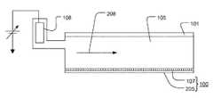
図1は、例示的な実施形態に従う核酸配列のためのシステムの構成要素のブロック図を例証する。本構成要素は、集積回路装置100上のフローセル101、基準電極108、シーケンシングのための複数の試薬114、弁ブロック116、洗浄溶液110、弁112、フルイディクス制御器118、ライン120/122/126、通路104/109/111、廃棄物容器106、アレイ制御器124、及びユーザインターフェース128を含む。集積回路装置100は、本明細書に記載されるような化学センサを含むセンサアレイの上に重なるマイクロウェルアレイ107を含む。フローセル101は、入口102、出口103、及びマイクロウェルアレイ107にわたる試薬114のための流路を画定するフローチャンバ105を含む。基準電極108は、通路111の内腔に挿入される流体通路またはワイヤを有する同心円筒をはじめとする、任意の好適な種類または形状であり得る。試薬114は、ポンプ、ガス圧力、真空、または他の好適な方法によって流体経路、弁、及びフローセル101に流され得、フローセル101の出口103を出た後、廃棄物容器106内に廃棄され得る。フルイディクス制御器118は、好適なソフトウェアを用いて、試薬114のための駆動力、ならびに弁112及び弁ブロック116の操作を制御し得る。 FIG. 1 illustrates a block diagram of the components of a system for nucleic acid sequences according to an exemplary embodiment. This component includes a
マイクロウェルアレイ107は、本明細書内ではマイクロウェルとも称される反応領域を含み、それは、センサアレイ内の対応する化学センサと動作的に関連付けられる。例えば、各反応領域は、検体またはその反応領域内の目的の反応特性を検知するために好適な化学センサに連結され得る。マイクロウェルアレイ107は、マイクロウェルアレイ107及びセンサアレイが単一の装置またはチップの一部であるように、集積回路装置100内に統合され得る。フローセル101は、マイクロウェルアレイ107にわたる試薬114の通路及び流量を制御するための様々な構成を有し得る。アレイ制御器124は、センサアレイの化学センサを読み込むために、バイアス電圧ならびにタイミング及び制御信号を集積回路装置100に提供する。アレイ制御器124はまた、基準バイアス電圧を基準電極108に提供して、マイクロウェルアレイ107にわたって流れる試薬114を付勢する。
実験中、アレイ制御器124は、バス127を介してセンサアレイの化学センサから集積回路装置100上の出力ポートまで出力信号を収集し、かつ処理する。アレイ制御器124は、コンピュータ、または他のコンピューティング手段であり得る。アレイ制御器124は、データ及びソフトウェアアプリケーションの記憶のためのメモリ、データにアクセスし、アプリケーションを実行するためのプロセッサ、ならびに図1内のシステムの様々な構成要素との通信を促進する構成要素を含み得る。例証される実施形態において、アレイ制御器124は、集積回路装置100の外部にある。いくつかの代替的な実施形態において、アレイ制御器124によって実施される機能のいくつかまたはすべては、集積回路装置100上の制御器または他のデータプロセッサによって実行される。化学センサからの出力信号の値は、マイクロウェルアレイ107内の対応する反応領域で起こる1つ以上の反応の物理的及び/または化学的パラメータを示す。例えば、例示的な実施形態において、出力信号の値は、それぞれが参照により本明細書に組み込まれる、2010年12月30日出願の米国仮特許出願第61/428,743号、及び2011年1月3日出願の同第61/429,328号に基づく2011年12月29日出願のRearickらの米国特許出願第13/339,846号、ならびに2010年12月29日出願の米国仮特許出願第61/428,097号に基づく2011年12月29日出願のHubbellの米国特許出願第13/339,753号に開示される技術を使用して処理され得る。ユーザインターフェース128は、フローセル101、及び集積回路装置100上のセンサアレイ内の化学センサから受信される出力信号に関する情報を表示し得る。ユーザインターフェース128はまた、機器の設定及び制御も表示し、ユーザが機器の設定及び制御を入力または設定することを可能にする。 During the experiment, the
フルイディクス制御器118は、個々の試薬114を規定の順序、規定の期間、規定の流量でフローセル101及び集積回路装置100へ送達することを制御し得る。次いでアレイ制御器124は、試薬114の送達に応答して発生する化学反応を示す化学センサの出力信号を収集及び分析することができる。実験中、システムはまた、反応が起こり、既知の規定の温度で測定が行われるように、集積回路装置100の温度を監視及び制御し得る。 The
システムは、操作中、多段階反応全体にわたって単一の流体または試薬を基準電極108に接触させるように構成され得る。弁112は、試薬114が流れている際にいかなる洗浄溶液110も通路109に流れ込むことを防ぐために閉鎖され得る。洗浄溶液の流動は止められ得るが、基準電極108と、通路109と、マイクロウェルアレイ107との間の絶え間ない流体、及び電気通信は依然として存在し得る。基準電極108と通路109及び111の合流点との間の距離は、通路109内を流れる(及びおそらくは通路111内に拡散する)試薬のわずかな量が基準電極108に達する、または全く達しないように、選択され得る。例示的な実施形態において、洗浄溶液110は、基準電極108と連続的に接触しているように選択され得、それは頻繁な洗浄工程を使用した多段階反応に特に有用である。 During operation, the system can be configured to contact a single fluid or reagent with the
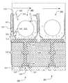
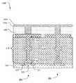
図2は、集積回路装置100及びフローセル101の一部分の横断及び拡大図を例証する。集積回路装置100は、センサアレイ205と動作的に関連付けられた反応領域のマイクロウェルアレイ107を含む。操作中、フローセル101のフローチャンバ105は、マイクロウェルアレイ107内の反応領域の開口端を横切って送達された試薬の試薬流動208を閉じ込める。反応領域の量、形状、横縦比(底幅対ウェル深さ比など)、及び他の寸法特徴は、起こる反応の性質、ならびに試薬、副産物、または(もしあれば)利用される標識技術に基づいて選択され得る。センサアレイ205の化学センサは、マイクロウェルアレイ107における関連付けられる反応領域内の化学反応に応答して(及び化学反応に関する出力信号を生成して)、検体または目的の反応特性を検出する。センサアレイ205の化学センサは、例えば、イオン感応性電界効果トランジスタ(ISFET)などの化学感応性電界効果トランジスタ(chemFET)であり得る。実施形態において使用され得る化学センサ及びアレイ構成の例は、それぞれが参照によりそれらの全体が本明細書に組み込まれる、2010年5月24日出願の表題「Fluidics System for Sequential Delivery of Reagents」のSchultzらの米国特許出願第12/785,667号(現米国特許第8,546,128号)、2010年3月10日出願の表題「Methods and Apparatus for Measuring Analytes Using Large Scale FET Arrays」のRotherbergらの米国特許出願第12/721,458号(現米国特許第8,306,757号)、2009年5月29日出願の表題「Methods and Apparatus for Measuring Analytes」のRotherbergらの米国特許出願第12/475,311号、2009年5月29日出願の表題「Methods and Apparatus for Measuring Analytes」のRotherbergらの米国特許出願第12/474,897号、2007年12月17日出願の表題「Methods and Apparatus for Measuring Analytes Using Large Scale FET Arrays」のRotherbergらの米国特許出願第12/002,781号、及び2005年8月1日出願の表題「Methods of Amplifying and Sequencing Nucleic Acids」の米国特許出願第12/474,897号(現米国特許第7,575,865号)に記載される。図3は、第1の実施形態に従う2つの代表的な化学センサ及びそれらの対応する反応領域の横断面図を例証する。 FIG. 2 illustrates a cross-sectional and enlarged view of a portion of
図3では、数百万の化学センサを含むことができるセンサアレイのほんの一部分を表す2つの化学センサ350、351が示される。化学センサ350は、対応する反応領域301に連結され、化学センサ351は、対応する反応領域302に連結される。化学センサ350は、センサアレイ内の化学センサの代表である。例証される実施形態において、化学センサ350は、化学感応性電界効果トランジスタ(chemFET)、より具体的には、本実施例ではイオン感応性電界効果トランジスタ(ISFET)である。化学センサ350は、導電性素子370によって反応領域301に連結されるセンサプレート320を有する浮遊ゲート構造体318を含む。図3に見られるように、センサプレート320は、浮遊ゲート構造体318内の一番上の浮遊ゲート導体である。例証される実施形態において、浮遊ゲート構造体318は、絶縁体材料319の層内に伝導性材料の複数のパターン層を含む。 In FIG. 3, two
化学センサ350はまた、半導体基板354内にソース領域321及びドレイン領域322も含む。ソース領域321及びドレイン領域322は、基板354の導電型とは異なる導電型を有するドープ半導体材料を備える。例えば、ソース領域321及びドレイン領域322は、ドープP型半導体材料を備え得、基板は、ドープN型半導体材料を備え得る。チャネル領域323は、ソース領域321とドレイン領域322とを分離する。浮遊ゲート構造体318は、チャネル領域323の上に重なり、ゲート絶縁体352によって基板354から分離される。ゲート絶縁体352は、例えば、二酸化ケイ素であり得る。代替的に、他の絶縁体がゲート絶縁体352に使用され得る。
図3に示されるように、反応領域301は、絶縁体材料310、308を通ってセンサプレート320の上面にまで延伸する側壁303を有する開口部内にある。絶縁体材料310、308のそれぞれは、二酸化ケイ素または窒化ケイ素などの材料の1つ以上の層を備え得る。開口部は、絶縁体材料308内にあり、かつセンサプレート320に近接する下部314を含む。開口部はまた、絶縁体材料310内にあり、かつ下部314から絶縁体材料310の上面に延伸する上部315も含む。例証される実施形態において、開口部の上部315の幅は、開口部の下部314の幅と実質的に同じである。しかしながら、開口部を作るために使用される材料(複数可)及び/またはエッチングプロセスに応じて、開口部の上部315の幅は、開口部の下部314の幅よりも大きくてもよく、またはその逆もあり得る。開口部は、例えば、円形断面を有してもよい。代替的に、開口部は非円形であってもよい。例えば、断面は、正方形、長方形、六角形、または不規則な形であってもよい。開口部の寸法及びそれらの傾斜は、実施形態に応じて様々であってもよい。いくつかの実施形態において、開口部は、平面断面面積(A)をPiで除算した数の4倍の平方根(例えば、sqrt(4×A/π))として定義される、特徴的な直径を有することができ、それは3.5マイクロメートル以下、2.0マイクロメートル以下、1.6マイクロメートル以下、1.0マイクロメートル以下、0.8マイクロメートル以下、0.6マイクロメートル以下、0.4マイクロメートル以下、0.2マイクロメートル以下、またはさらに0.1マイクロメートル以下などの、5マイクロメートル以下である。 As shown in FIG. 3, the
開口部の下部314は、絶縁体材料310の側壁303上に導電性素子370を含む。例証される実施形態において、導電性素子370の内面371は、反応領域301の下方部分を画定する。つまり、導電性素子370の内面371と化学センサ350のための反応領域301との間に介在して堆積される材料層は存在しない。この構造体の結果として、導電性素子370の内面371は、開口部に共形し、化学センサ350のための検知表面として働く。導電性素子370の精密な形状及び寸法は、図面に例証される他のすべての材料と同様に、プロセスに依存することが当業者によって理解されるべきである。 The
例証される実施形態において、導電性素子370は、導電性素子370がセンサプレート320の上面を横切って延伸するような、開口部の下部314内の材料の共形(conformal)層である。例証される実施形態において、導電性素子370は、開口部の下部314を超えて開口部の上部315内に延伸する。絶縁体材料310の内面は、反応領域301の上方部分を画定する。伝導性素子370は、例えば、側壁303の少なくとも5%、側壁303の少なくとも10%、少なくとも25%、少なくとも50%、少なくとも75%、もしくは少なくとも85%に沿って延伸し得るか、または側壁303の99%に沿って延伸さえし得る。導電性素子370の共形内面371は、化学センサ350が小さい平面面積を有しながら、小さい検知表面に関連したノイズ問題を回避するのに十分に大きい表面積も有することを可能にする。化学センサ350の平面面積を、反応領域301の幅(または直径)によって部分的に決定し、小さく作製することができ、高密度アレイを可能にする。加えて、検知表面は側壁303上方へ延伸するため、検知表面積は、この延伸の距離及び反応領域301の円周次第であり、比較的大きくてもよい。結果として、低ノイズ化学センサ350、351を、反応の特徴を正確に検出することができるように、高密度アレイで提供することができる。 In the illustrated embodiment, the
本装置の製造及び/または操作中、導電性素子370の材料の薄酸化物が成長し得、それは化学センサ350のための検知材料(例えば、イオン感応性検知材料)として働く。酸化物が形成されるかどうかは、伝導性材料、実施される製造プロセス、及び装置が操作される条件次第である。例えば、一実施形態において、導電性素子370は窒化チタンであり得、酸化チタンまたは酸窒化チタンは、製造中及び/または使用中の溶液への曝露中に伝導性素子370の内面371上で成長し得る。例証される実施形態において、導電性素子370は、材料の単一層として示される。より一般的には、導電性素子370は、実施形態に応じて、金属またはセラミックスなどの様々な導電性材料の1つ以上の層を備え得る。伝導性材料は、例えば、金属材料もしくはその合金であってもよく、またはセラミック材料、あるいはその組み合わせであってもよい。例示的な金属材料は、アルミニウム、銅、ニッケル、チタン、銀、金、プラチナ、ハフニウム、ランタン、タンタル、タングステン、リジウム、ジルコニウム、パラジウム、またはそれらの組み合わせのうちの1つを含む。例示的なセラミック材料は、窒化チタン、窒化チタンアルミニウム、酸窒化チタン、窒化タンタル、またはそれらの組み合わせのうちの1つを含む。いくつかの代替的な実施形態において、追加の共形検知材料(示されていない)が、伝導性素子370上及び開口部内に堆積される。検知材料は、特定のイオンに対する感応性を促進するために様々な異なる材料のうちの1つ以上を備え得る。例えば、窒化ケイ素または酸窒化ケイ素、ならびに酸化ケイ素、アルミニウムまたは酸化タンタルなどの酸化金属が、一般的に、水素イオンに対する感応性を提供する一方、バリノマイシンを含有するポリ塩化ビニルを含有する検知材料は、カリウムイオンに対する感応性を提供する。ナトリウム、銀、鉄、臭素、ヨウ素、カルシウム、及び硝酸塩などの他のイオンに対して感応する材料もまた、実施形態に応じて使用され得る。 During manufacture and/or operation of the device, a thin oxide of the
操作中、反応物、洗浄溶液、及び他の試薬は、拡散機構340によって、反応領域301内を、及びそこから外へ移動し得る。化学センサ350は、伝導性素子370に近接する電荷324の量に応答する(及び伝導性素子の量に関する出力信号を生成する)。検体溶液中の電荷324の存在は、反応領域301内の伝導性素子370と検体溶液との間の界面で表面電位を変更する。電荷324の変化は、浮遊ゲート構造体318上の電圧の変化を引き起こし、それが今度はトランジスタの閾値電圧を変化させる。閾値電圧におけるこの変化は、ソース領域321とドレイン領域322との間のチャネル領域323内の電流を測定することによって測定することができる。結果として、化学センサ350を直接使用して、ソース領域321もしくはドレイン領域322に連結されるアレイライン上に電流ベースの出力信号を提供するか、または非直接的に追加の電気回路構成を用いて電圧ベースの出力信号を提供することができる。電荷324は、反応領域301の底部近くでより高濃度であり得るため、伝導性素子370が開口部の側壁303の上方に延伸する距離は、電荷324に応答して検出される所望の信号の振幅と、伝導性素子370と検体溶液との間の電荷の無作為変動に起因する流体ノイズとの間のトレードオフである。伝導性素子370が側壁303の上方に延伸する距離が増加すると、化学センサ350のための流体界面積が増加し、それが流体ノイズを低減するように働く。しかしながら、反応領域301からの電荷324の拡散が原因で、電荷324の濃度は、反応領域301の底部からの距離とともに減少する。結果として、伝導性素子370の上方側壁部分は、より低い電荷濃度を有する区域からの信号の部分を検出し、それによってセンサ350によって検出される所望の信号の全体の振幅を低減することができる。反対に、伝導性素子370が側壁303の上方に延伸する距離が減少すると、検知表面積は減少し、従って流体ノイズは増加するが、センサ350によって検出される所望の信号の全体の振幅も増加する。 During operation, reactants, wash solutions, and other reagents can move in and out of
非常に小さい検知表面積では、出願者らは、流体ノイズが、所望の信号の振幅とは異なって、検知表面積の関数として変化することを発見している。センサ出力信号のSNRはこれら2つの数量の比であるため、伝導性素子370が、SNRが最大である側壁303に沿って延伸する最適距離が存在する。最適距離は、伝導性素子370及び絶縁体材料310の材料特徴、反応領域の量、形状、横縦比(底幅対ウェル深さ比など)、及び他の寸法特徴、起こる反応の性質、ならびに試薬、副産物、または(もしあれば)利用される標識技術に応じて、実施形態によって様々であり得る。最適距離は、例えば、経験的に決定され得る。 At very small sensing surface areas, Applicants have found that fluid noise varies as a function of sensing surface area, as opposed to the amplitude of the desired signal. Since the SNR of the sensor output signal is the ratio of these two quantities, there is an optimum distance that the
図4〜12に関して下記により詳細に記載されるように、伝導性素子370が側壁303に沿って延伸する距離は、例えば、堆積された層のエッチング時間によって画定される。絶縁体材料310及び導電性素子370を、例えば、距離309の選択性をもたらす(例えば、絶縁体材料310が導電性素子370を超えて延伸する距離)、時限エッチングプロセスを使用してエッチングすることができる。そうすることで、化学センサの表面積を制御することができ、アレイにわたって均一な化学センサ性能をもたらし、下流信号処理を簡略化する。 As described in more detail below with respect to FIGS. 4-12, the distance that
ある実施形態において、反応領域301内で実行される反応は、目的の検体の特徴または特性を識別または決定するための分析反応であり得る。そのような反応は、導電性素子370に隣接する電荷の量に影響を与える副産物を直接または間接的に生成することができる。そのような副産物が少量で産生されるか、または急速に崩壊する、もしくは他の構成物質と反応する場合、生成される出力信号を増加させるために、同じ検体の複数の複製が、反応領域301内で同時に分析され得る。ある実施形態において、検体の複数の複製は、反応領域301内への堆積前または後のいずれかに、図3に示されるように、固相支持体312に結合され得る。固相支持体312は、ミクロ粒子、ナノ粒子、ビーズ、固体もしくは多孔質ゲル等であり得る。単純かつ容易な説明のため、固相支持体312は、本明細書内では粒子とも称される。核酸検体では、複数の、接続された複製が、ローリングサークル増幅(RCA)、急激なRCA、リコンビナーゼポリメラーゼ増幅(RPA)、ポリメラーゼ連鎖反応増幅(PCR)、エマルジョンPCR増幅、または同様の技術によって作製され、固体支持体を必要とせずにアンプリコンを産生し得る。 In certain embodiments, the reaction performed in
様々な例示的な実施形態において、本明細書に記載される方法、システム、及びコンピュータ可読媒体を有利に使用して、電子もしくは電荷ベースの核酸シーケンシングから獲得されるデータもしくは信号を処理及び/または分析してもよい。電子または電荷ベースのシーケンシング(pHベースのシーケンシングなど)において、ヌクレオチド取り込み事象は、ポリメラーゼ触媒ヌクレオチド伸長反応の自然の副産物として生成されるイオン(例えば、水素イオン)を検出することによって決定され得る。これは、試料またはテンプレート核酸をシーケンスするために使用され得、この試料またはテンプレート核酸は、目的の核酸配列の断片であり得、例えば、クローン集団として粒子、ミクロ粒子、ビーズ等などの固体支持体に直接的または非直接的に結合され得る。試料またはテンプレート核酸は、プライマー及びポリメラーゼに作動的に関連付けられ得、デオキシヌクレオシド三リン酸(「dNTP」)付加の繰り返される循環または「流動」(本明細書内ではヌクレオチド取り込みが生じ得る「ヌクレオチド流動」と称され得る)、及び洗浄に供され得る。プライマーは、テンプレート内の次の塩基を補足するdNTPが添加されるたびに、プライマーの3’末端をポリメラーゼによって延伸することができるように、試料またはテンプレートに焼鈍され得る。次いで、ヌクレオチド流動の既知の配列、及び各ヌクレオチド流動中のイオン濃度を示す化学センサの測定された出力信号に基づき、化学センサに連結される反応領域内に存在する試料核酸と関連付けられるヌクレオチド(複数可)の種類、配列、及び数を決定することができる。 In various exemplary embodiments, the methods, systems, and computer readable media described herein are advantageously used to process and/or process data or signals obtained from electronic or charge-based nucleic acid sequencing. Or it may be analyzed. In electronic or charge-based sequencing (such as pH-based sequencing), nucleotide incorporation events can be determined by detecting ions (eg, hydrogen ions) that are generated as a natural byproduct of a polymerase-catalyzed nucleotide extension reaction. .. It can be used to sequence a sample or template nucleic acid, which can be a fragment of the nucleic acid sequence of interest, e.g. as a clonal population, a solid support such as particles, microparticles, beads, etc. Can be bound directly or indirectly. A sample or template nucleic acid can be operatively associated with the primer and polymerase and can be cycled or "flowed" in repeated cycles of deoxynucleoside triphosphate ("dNTP") addition (wherein nucleotide incorporation can occur "nucleotide flow"). ,” and may be subjected to washing. The primer can be annealed to the sample or template so that the 3'end of the primer can be extended by a polymerase each time a dNTP that complements the next base in the template is added. Then, based on the known sequence of nucleotide fluxes and the measured output signal of the chemical sensor indicative of the ion concentration in each nucleotide flux, the nucleotides (plurality Yes) type, sequence, and number can be determined.
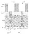
図4〜12は、第1の実施形態に従う化学センサ及び対応する反応領域のアレイを形成するための製造プロセスにおける段階を例証する。図4は、第1の段階で形成される構造体400を例証する。構造体400は、化学センサ350、351のための浮遊ゲート構造体(例えば、浮遊ゲート構造体318)を含む。構造体400は、ゲート絶縁体材料の層を半導体基板354上に堆積すること、及びポリシリコンの層(または他の導電性材料)をゲート絶縁体材料の層の上に堆積することによって形成することができる。次いで、ポリシリコンの層及び層ゲート絶縁体材料を、エッチマスクを使用してエッチングし、ゲート絶縁体素子(例えば、ゲート絶縁体352)、及び浮遊ゲート構造体の一番下の伝導性材料素子を形成することができる。イオン注入マスクの形成に続き、次いでイオン注入を実施し、化学センサのソース及びドレイン領域(例えば、ソース領域321及びドレイン領域322)を形成することができる。次いで絶縁体材料319の第1の層を、一番下の伝導性材料素子の上に堆積することができる。次いで伝導性プラグを絶縁体材料319の第1の層内でエッチングされるビア内に形成し、浮遊ゲート構造体の一番下の伝導性材料素子に接触させることができる。次いで伝導性材料の層を絶縁体材料319の第1の層の上に堆積し、かつパターン形成して、伝導性プラグに電気的に接続される第2の伝導性材料素子を形成することができる。次いでこのプロセスを複数回繰り返し、図4に示される完全な浮遊ゲート構造体318を形成することができる。代替的に、他の及び/または追加の技術を実施して本構造体を形成してもよい。図4内の構造体400を形成することはまた、本明細書に記載される化学センサが実装される装置及びアレイ構成に応じて、化学センサを操作するために使用される、化学センサにアクセスするためのアレイライン(例えば、行ライン、列ライン等)、基板354内の追加のドープ領域、及び他の電気回路構成(例えば、スイッチを選択する、電気回路構成にアクセスする、電気回路構成を付勢する等)などの追加の素子を形成することを含むこともできる。いくつかの実施形態において、本構造体の素子は、例えば、参照によりそれらの全体が上記に組み込まれた、2010年5月24日出願の表題「Fluidics System for Sequential Delivery of Reagents」のSchultzらの米国特許出願第12/785,667号(現米国特許第8,546,128号)、2010年3月10日出願の表題「Methods and Apparatus for Measuring Analytes Using Large Scale FET Arrays」のRotherbergらの米国特許出願第12/721,458号(現米国特許第8,306,757号)、2009年5月29日出願の表題「Methods and Apparatus for Measuring Analytes」のRotherbergらの米国特許出願第12/475,311号、2009年5月29日出願の表題「Methods and Apparatus for Measuring Analytes」のRotherbergらの米国特許出願第12/474,897号、2007年12月17日出願の表題「Methods and Apparatus for Measuring Analytes Using Large Scale FET Arrays」のRotherbergらの米国特許出願第12/002,781号、及び2005年8月1日出願の表題「Methods of Amplifying and Sequencing Nucleic Acids」の米国特許出願第12/474,897号(現米国特許第7,575,865号)に記載される技術を使用して製造され得る。 4-12 illustrate steps in a manufacturing process for forming an array of chemical sensors and corresponding reaction regions according to the first embodiment. FIG. 4 illustrates the
次に、所与の厚さを有する絶縁体材料308を、図4に例証される構造体400の上に堆積し、図5に例証される構造体をもたらす。絶縁体材料308は、絶縁体の1つ以上の絶縁体層を備える。絶縁体材料308は、アレイにわたって厚さの極めて小さな変動をもたらすプロセスを使用して堆積され得る。例えば、絶縁体材料308は、酸化ケイ素を含み得、かつ高密度プラズマ(HDP)堆積を使用して堆積され得る。スパッタリング、反応性スパッタリング、原子層堆積(ALD)、低圧化学気相堆積(LPCVD)、プラズマ増強化学気相堆積(PECVD)、金属有機化学気相堆積(MOCVD)等などの、様々な技術が使用され得る。次に、図5内の構造体の絶縁体材料308をエッチングし、化学センサ350、351の浮遊ゲート構造体の上面にまで延伸する空洞600、602を形成し、図6に例証される構造体をもたらす。空洞600、602は、例えば、絶縁体材料308上にフォトレジストの層をパターン形成して、空洞600、602の位置を画定し、次いでパターン形成されたフォトレジストを使用して絶縁体材料308を異方性エッチングする、石版プロセスを使用して形成され得る。絶縁体材料308の異方性エッチングは、例えば、フッ素ベースの反応性イオンエッチング(RIE)プロセスなど、ドライエッチングであり得る。次に、絶縁体材料310を図6に例証される構造体上に形成し、図7に例証される構造体をもたらす。絶縁体材料310は、二酸化ケイ素または窒化ケイ素など、堆積された絶縁体材料の1つ以上の層を備え得る。 Next, an
次に、絶縁体材料310をエッチングして、センサプレート320にまで延伸する反応領域301、302を画定する開口部を形成し、図8に例証される構造体をもたらす。次に、伝導性材料900の共形層を図8に例証される構造体上に堆積し、図9に例証される構造体をもたらす。伝導性材料900は、導電性材料の1つ以上の層を備える。例えば、伝導性材料900は、窒化チタンの層、またはチタンの層であり得る。代替的に、伝導性素子370に関して上に記載されるようなものなど、他の及び/または追加の伝導性材料を使用してもよい。加えて、伝導性材料の1つを超える層を堆積してもよい。伝導性材料900は、スパッタリング、反応性スパッタリング、原子層堆積(ALD)、低圧化学気相堆積(LPCVD)、プラズマ増強化学気相堆積(PECVD)、金属有機化学気相堆積(MOCVD)等などの、様々な技術を使用して堆積され得る。 Next, the
次に、材料1000を図9に例証される構造体上に形成し、図10に例証される構造体をもたらす。材料1000は、二酸化ケイ素または窒化ケイ素など、堆積された絶縁体材料の1つ以上の層を備え得る。代替的に、材料1000はフォトレジストを含み得る。一実施形態において、材料1000がフォトレジストを含む場合、絶縁体材料310の距離309があらわになる(つまり、側壁303の距離309が曝露される)ように材料1000及び伝導性材料900の部分エッチングが実施され、図11に例証される構造体をもたらす。材料1000及び導電性材料900を、使用されるプロセス及び/もしくは材料(複数可)に応じて、一緒に、または別々に、エッチングしてもよい。例えば、部分エッチングは、O2レジストエッチング、Arスパッタブレイクスルーエッチング、及び臭化水素チタンエッチングのうちの少なくとも1つを使用して実施され得る。次に、材料1000をエッチングして、伝導性素子370、900にまで延伸する反応領域301、302を画定する開口部を形成し、図12に例証される構造体をもたらす。一実施形態において、残存フォトレジストは、当業者に既知の技術、例えば、O2プラズマアッシュを使用して、開口部から除去される必要があり得る。
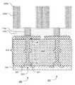
図13は、第2の実施形態に従う2つの代表的な化学センサ及びそれらの対応する反応領域の横断面図を例証する。図13に例証される2つの代表的な化学センサの構造体は、図13はセンサプレート320上にビアを含み、その上にマイクロウェル/ナノウェルが構築されるという点で、一態様において、図3に例証される2つの代表的な化学センサとは異なる。したがって、図3内の構造体の製作は、以下にもっと詳細に説明されるような図13の構造体の製作とは異なる。 FIG. 13 illustrates a cross-sectional view of two representative chemical sensors and their corresponding reaction zones according to the second embodiment. The structure of the two exemplary chemical sensors illustrated in FIG. 13 is, in one aspect, a diagram in that FIG. 13 includes vias on the
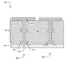
図14〜25は、例示的な実施形態に従う化学装置のアレイ及び対応するウェル構造体を形成するための製造プロセスにおける段階を例証する。図14は、化学装置350、351のための浮遊ゲート構造体(例えば、浮遊ゲート構造体318)を含む構造体1400を例証する。構造体1400を、図4に関して上に詳細に記載される構造体400に従って形成することができる。図15に例証される構造体1500内に例証されるように、絶縁体材料1503は、化学装置350の電界効果トランジスタのセンサプレート320上に形成され得る。次に、図16に例証されるように、図15内の構造体1500の絶縁体材料1503をエッチングして、化学装置350、351の浮遊ゲート構造体の上面にまで延伸する開口部1618、1620(ビアのため)を形成し、図16に例証される構造体1600をもたらす。開口部1618、1620は、例えば、絶縁体材料1503上にフォトレジストの層をパターン形成して、開口部1618、1620の位置を画定し、次いでパターン形成されたフォトレジストをエッチマスクとして使用して絶縁体材料1503を異方性エッチングする、リソグラフィプロセスを使用して形成され得る。絶縁体材料1503の異方性エッチングは、例えば、フッ素ベースの反応性イオンエッチング(RIE)プロセスなど、ドライエッチングであり得る。例証される実施形態において、開口部1618、1620は、距離1630によって分離され、開口部1618、1620は、ビアのための好適な寸法である。例えば、分離距離1630は、開口部1618、1620を形成するために使用されるプロセス(例えば、リソグラフィプロセス)のための最小形状であり得る。そのような場合、距離1630は、幅1620よりも著しく大きくてもよい。次に、伝導性材料1704の層を図16に例証される構造体1600上に堆積し、図17に例証される構造体1700をもたらす。伝導性材料1704は、伝導性ライナーと称され得る。伝導性材料1704は、導電性材料の1つ以上の層を備え得る。例えば、伝導性材料1704は、窒化チタンの層、またはチタンの層であり得る。代替的に、導電性素子に関して上に記載されるようなものなど、他の及び/または追加の伝導性材料を使用してもよい。加えて、伝導性材料の1つを超える層を堆積してもよい。伝導性材料1704は、スパッタリング、反応性スパッタリング、原子層堆積(ALD)、低圧化学気相堆積(LPCVD)、プラズマ増強化学気相堆積(PECVD)、金属有機化学気相堆積(MOCVD)等などの、様々な技術を使用して堆積され得る。 14-25 illustrate steps in a manufacturing process for forming an array of chemical devices and corresponding well structures according to an exemplary embodiment. FIG. 14 illustrates a
次に、タングステンなどの伝導性材料1805の層を図17に例証される構造体1700上に堆積し、図18に例証される構造体1800をもたらす。伝導性材料1805は、スパッタリング、反応性スパッタリング、原子層堆積(ALD)、低圧化学気相堆積(LPCVD)、プラズマ増強化学気相堆積(PECVD)、金属有機化学気相堆積(MOCVD)等、または任意の他の好適な技術などの、様々な技術を使用して堆積され得る。次に、伝導性材料1704及び伝導性材料1805を、化学的機械研磨(CMP)プロセスを使用して平面化し、例えば、図19に例証される構造体1900をもたらす。任意の追加の工程として、ビアバリアライナー(示されない)を、平面化した伝導性材料1704及び伝導性材料1805の上に形成し得る。例えば、ビアバリアライナーは、窒化チタンを含む。 Next, a layer of
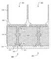
次に、絶縁体材料2006を図19に例証される構造体上に形成し、図20に例証される構造体をもたらす。絶縁体材料2006は、二酸化ケイ素または窒化ケイ素など、堆積された絶縁体材料の1つ以上の層を備え得る。次に、絶縁体材料2006をエッチングして、平面化した伝導性材料1704及び伝導性材料1805、ならびに絶縁体材料1503にまで延伸する開口部を形成し、図21に例証される構造体をもたらす。絶縁体材料1503は、例証される実施形態に見られるように、伝導性材料1704及び伝導性材料1805が絶縁体材料1503より高く上げられて開口部内に突き出るように形成されるとき、部分的にエッチングされ得る。次に、伝導性材料2200の共形層を図21に例証される構造体上に堆積し、図22に例証される構造体をもたらす。伝導性材料2200は、導電性材料の1つ以上の層を備える。例えば、伝導性材料2200は、窒化チタンの層、またはチタンの層であり得る。代替的に、伝導性素子370に関して上に記載されるようなものなど、他の及び/または追加の伝導性材料を使用してもよい。加えて、伝導性材料の1つを超える層を堆積してもよい。伝導性材料2200は、スパッタリング、反応性スパッタリング、原子層堆積(ALD)、低圧化学気相堆積(LPCVD)、プラズマ増強化学気相堆積(PECVD)、金属有機化学気相堆積(MOCVD)等などの、様々な技術を使用して堆積され得る。
次に、材料2300を図22に例証される構造体上に形成し、図23に例証される構造体をもたらす。材料2300は、二酸化ケイ素または窒化ケイ素など、堆積された絶縁体材料の1つ以上の層を備え得る。代替的に、材料2300はフォトレジストを含み得る。一実施形態において、材料2300がフォトレジストを含む場合、絶縁体材料310の距離1309があらわになる(つまり、側壁1303の距離309が曝露される)ように材料2300及び伝導性材料2200の部分エッチングが実施され、図24に例証される構造体をもたらす。材料2300及び導電性材料2200を、使用されるプロセス及び/もしくは材料(複数可)に応じて、一緒に、または別々に、エッチングしてもよい。例えば、部分エッチングは、O2レジストエッチング、Arスパッタブレイクスルーエッチング、及び臭化水素チタンエッチングのうちの少なくとも1つを使用して実施され得る。次に、材料2300をエッチングして、伝導性素子370、2200にまで延伸する反応領域301、302を画定する開口部を形成し、図25に例証される構造体をもたらす。一実施形態において、残存フォトレジストは、当業者に既知の技術、例えば、O2プラズマアッシュを使用して、開口部から除去される必要があり得る。
本発明は、上に詳述される好ましい実施形態及び実施例を参照して開示されるが、これらの実施例は、制限する意味ではなく例証する意味で意図されることを理解されたい。変形及び組み合わせが当業者には容易に想到されることが企図され、その変形及び組み合わせは、本発明の趣旨及び以下の特許請求の範囲の範囲内であるものとする。 While the present invention is disclosed with reference to the preferred embodiments and examples detailed above, it is to be understood that these examples are intended in an illustrative rather than a limiting sense. It is contemplated that variations and combinations will readily occur to those skilled in the art, which variations and combinations are within the spirit of the invention and the scope of the following claims.
Claims (19)
Translated fromJapanese上面を有する浮遊ゲート導体を含む化学感応性電界効果トランジスタと、
前記浮遊ゲート導体の前記上面にまで延伸する開口部を画定する材料であって、第2の絶縁体の下にある第1の絶縁体を備える材料と、
前記浮遊ゲート導体の前記上面に接触し、かつ前記開口部の側壁に沿ってある距離を延伸する伝導性素子と、を備える、前記化学センサ。A chemical sensor,
A chemically sensitive field effect transistor including a floating gate conductor having a top surface;
A material defining an opening extending to the top surface of the floating gate conductor, the material comprising a first insulator underlying a second insulator;
A conductive element contacting the top surface of the floating gate conductor and extending a distance along a sidewall of the opening.
上面を有する浮遊ゲート導体を含む化学感応性電界効果トランジスタを形成することと、
前記浮遊ゲート導体の前記上面にまで延伸する開口部を画定する材料を形成することであって、前記材料が第2の絶縁体の下にある第1の絶縁体を備える、形成することと、
前記浮遊ゲート導体の前記上面に接触し、かつ前記開口部の側壁に沿ってある距離を延伸する伝導性素子を形成することと、を含む、前記方法。A method of manufacturing a chemical sensor, comprising:
Forming a chemically sensitive field effect transistor including a floating gate conductor having a top surface;
Forming a material defining an opening extending to the upper surface of the floating gate conductor, the material comprising a first insulator underlying a second insulator;
Forming a conductive element contacting the top surface of the floating gate conductor and extending a distance along a sidewall of the opening.
前記浮遊ゲート導体上に前記第1の絶縁体を形成することであって、前記第1の絶縁体が前記浮遊ゲート導体の前記上面にまで延伸する空洞を画定する、形成することと、
その上に前記第2の絶縁体を形成することと、
前記伝導性素子を曝露するために、前記第2の絶縁体をエッチングし、それによって開口部を画定することと、
前記開口部内に前記伝導性素子を形成することと、を含む、請求項11に記載の前記方法。Forming the material and forming the conductive element,
Forming the first insulator on the floating gate conductor, the first insulator defining a cavity extending to the upper surface of the floating gate conductor;
Forming the second insulator thereon, and
Etching the second insulator to expose the conductive element, thereby defining an opening;
Forming the conductive element in the opening.
伝導性材料を前記開口部内かつ前記第1の絶縁体の上面上に堆積することと、
前記伝導性材料の少なくとも一部分を前記第2の絶縁体の前記上面から取り除くことと、を含む、請求項12に記載の前記方法。Forming the conductive element in the opening,
Depositing a conductive material in the opening and on the top surface of the first insulator;
Removing at least a portion of the conductive material from the top surface of the second insulator.
前記開口部内のフォトレジストの層を堆積することと、
前記伝導性材料の少なくとも一部分を、前記フォトレジストと一緒に、前記第2の絶縁体の前記上面から取り除くことと、を含む、請求項13に記載の前記方法。Removing at least the portion of the conductive material,
Depositing a layer of photoresist in the opening,
14. The method of claim 13, comprising: removing at least a portion of the conductive material with the photoresist from the top surface of the second insulator.
Applications Claiming Priority (4)
| Application Number | Priority Date | Filing Date | Title |
|---|---|---|---|
| US201361790866P | 2013-03-15 | 2013-03-15 | |
| US61/790,866 | 2013-03-15 | ||
| US201361900907P | 2013-11-06 | 2013-11-06 | |
| US61/900,907 | 2013-11-06 |
Related Parent Applications (1)
| Application Number | Title | Priority Date | Filing Date |
|---|---|---|---|
| JP2016500687ADivisionJP2016510895A (en) | 2013-03-15 | 2014-03-05 | Chemical sensor with consistent sensor surface area |
Publications (3)
| Publication Number | Publication Date |
|---|---|
| JP2020042034A JP2020042034A (en) | 2020-03-19 |
| JP2020042034A5 JP2020042034A5 (en) | 2020-06-11 |
| JP2020042034A6true JP2020042034A6 (en) | 2020-06-25 |
Family
ID=50349935
Family Applications (2)
| Application Number | Title | Priority Date | Filing Date |
|---|---|---|---|
| JP2016500687APendingJP2016510895A (en) | 2013-03-15 | 2014-03-05 | Chemical sensor with consistent sensor surface area |
| JP2019199636APendingJP2020042034A (en) | 2013-03-15 | 2019-11-01 | Chemical sensor with consistent sensor surface area |
Family Applications Before (1)
| Application Number | Title | Priority Date | Filing Date |
|---|---|---|---|
| JP2016500687APendingJP2016510895A (en) | 2013-03-15 | 2014-03-05 | Chemical sensor with consistent sensor surface area |
Country Status (5)
| Country | Link |
|---|---|
| US (3) | US20140264472A1 (en) |
| EP (1) | EP2972280B1 (en) |
| JP (2) | JP2016510895A (en) |
| CN (1) | CN105264366B (en) |
| WO (1) | WO2014149780A1 (en) |
Families Citing this family (22)
| Publication number | Priority date | Publication date | Assignee | Title |
|---|---|---|---|---|
| CA2672315A1 (en) | 2006-12-14 | 2008-06-26 | Ion Torrent Systems Incorporated | Methods and apparatus for measuring analytes using large scale fet arrays |
| US8776573B2 (en) | 2009-05-29 | 2014-07-15 | Life Technologies Corporation | Methods and apparatus for measuring analytes |
| JP2013540259A (en) | 2010-06-30 | 2013-10-31 | ライフ テクノロジーズ コーポレーション | Array column integrator |
| WO2012003363A1 (en) | 2010-06-30 | 2012-01-05 | Life Technologies Corporation | Ion-sensing charge-accumulation circuits and methods |
| US11307166B2 (en) | 2010-07-01 | 2022-04-19 | Life Technologies Corporation | Column ADC |
| US9970984B2 (en) | 2011-12-01 | 2018-05-15 | Life Technologies Corporation | Method and apparatus for identifying defects in a chemical sensor array |
| US9841398B2 (en) | 2013-01-08 | 2017-12-12 | Life Technologies Corporation | Methods for manufacturing well structures for low-noise chemical sensors |
| JP6671274B2 (en) | 2013-03-15 | 2020-03-25 | ライフ テクノロジーズ コーポレーション | Chemical device with thin conductive element |
| EP2972280B1 (en)* | 2013-03-15 | 2021-09-29 | Life Technologies Corporation | Chemical sensor with consistent sensor surface areas |
| US10458942B2 (en) | 2013-06-10 | 2019-10-29 | Life Technologies Corporation | Chemical sensor array having multiple sensors per well |
| US9023674B2 (en)* | 2013-09-20 | 2015-05-05 | Taiwan Semiconductor Manufacturing Company, Ltd. | Biosensing well array with protective layer |
| KR102593647B1 (en) | 2014-12-18 | 2023-10-26 | 라이프 테크놀로지스 코포레이션 | High data rate integrated circuit with transmitter configuration |
| US10077472B2 (en) | 2014-12-18 | 2018-09-18 | Life Technologies Corporation | High data rate integrated circuit with power management |
| JP6352843B2 (en)* | 2015-03-24 | 2018-07-04 | 東芝メモリ株式会社 | Semiconductor memory device |
| CN107923869B (en)* | 2015-08-25 | 2021-10-08 | 生命技术公司 | Design of deep microwell and method of making the same |
| CN108291251A (en) | 2015-09-22 | 2018-07-17 | 生命技术公司 | System and method for foranalysis of nucleic acids |
| EP3510388A1 (en)* | 2016-09-09 | 2019-07-17 | Life Technologies Corporation | Chemically-sensitive field-effect transistor with microwell structure and method for producing the same |
| WO2018187511A1 (en)* | 2017-04-04 | 2018-10-11 | Life Technologies Corporation | Method for making a well disposed over a sensor |
| CN107090404B (en)* | 2017-04-21 | 2019-08-13 | 京东方科技集团股份有限公司 | A kind of gene sequencing chip and gene order surveying method, gene sequencing device |
| US11338294B2 (en) | 2017-04-27 | 2022-05-24 | Polybiomics, Inc. | Orthogonal polybiosensing and imaging systems |
| EP3615921A4 (en)* | 2017-04-27 | 2021-04-14 | Polybiomics, Inc. | Orthogonal polybiosensing and imaging systems |
| CN112585459B (en)* | 2018-08-17 | 2024-01-02 | 生命技术公司 | Method of forming an ion sensor |
Family Cites Families (521)
| Publication number | Priority date | Publication date | Assignee | Title |
|---|---|---|---|---|
| US3531258A (en) | 1967-11-16 | 1970-09-29 | Us Health Education & Welfare | Apparatus for the automated synthesis of peptides |
| DE2413703C3 (en) | 1974-03-21 | 1979-01-04 | Max-Planck-Gesellschaft Zur Foerderung Der Wissenschaften E.V., 3400 Goettingen | Valve arrangement for the supply of liquid or gaseous substances to a processing vessel |
| JPS5530312B2 (en) | 1975-01-16 | 1980-08-09 | ||
| US5132418A (en) | 1980-02-29 | 1992-07-21 | University Patents, Inc. | Process for preparing polynucleotides |
| JPS57136158A (en) | 1981-02-17 | 1982-08-23 | Sumitomo Electric Ind Ltd | Ph electrode |
| GB2096824A (en) | 1981-04-09 | 1982-10-20 | Sibbald Alastair | Chemically sensitive field effect transistor |
| EP0065202B1 (en) | 1981-05-15 | 1986-03-12 | Licentia Patent-Verwaltungs-GmbH | Method for measuring ionic concentrations |
| FR2510260A1 (en) | 1981-07-24 | 1983-01-28 | Suisse Fond Rech Microtech | ION-SENSITIVE SEMICONDUCTOR DEVICE |
| US4438354A (en) | 1981-08-14 | 1984-03-20 | American Microsystems, Incorporated | Monolithic programmable gain-integrator stage |
| US4411741A (en) | 1982-01-12 | 1983-10-25 | University Of Utah | Apparatus and method for measuring the concentration of components in fluids |
| US4558845A (en) | 1982-09-22 | 1985-12-17 | Hunkapiller Michael W | Zero dead volume valve |
| NL8302964A (en) | 1983-08-24 | 1985-03-18 | Cordis Europ | DEVICE FOR DETERMINING THE ACTIVITY OF AN ION (PION) IN A LIQUID. |
| NL8303792A (en) | 1983-11-03 | 1985-06-03 | Cordis Europ | Apparatus provided with an measuring circuit based on an ISFET; ISFET SUITABLE FOR USE IN THE MEASURING CIRCUIT AND METHOD FOR MANUFACTURING AN ISFET TO BE USED IN THE MEASURING CIRCUIT |
| JPS60128345A (en) | 1983-12-15 | 1985-07-09 | Olympus Optical Co Ltd | Measuring device for ion concentration |
| US4660063A (en) | 1985-03-18 | 1987-04-21 | General Electric Company | Immersion type ISFET |
| DE3513168A1 (en) | 1985-04-12 | 1986-10-16 | Thomas 8000 München Dandekar | BIOSENSOR CONSISTING OF A SEMICONDUCTOR BASED ON SILICON OR CARBON-BASED (ELECTRONIC PART) AND NUCLEIN BASE (OR. OTHER BIOL. MONOMERS) |
| US4743954A (en) | 1985-06-07 | 1988-05-10 | University Of Utah | Integrated circuit for a chemical-selective sensor with voltage output |
| US4863849A (en) | 1985-07-18 | 1989-09-05 | New York Medical College | Automatable process for sequencing nucleotide |
| EP0213825A3 (en) | 1985-08-22 | 1989-04-26 | Molecular Devices Corporation | Multiple chemically modulated capacitance |
| GB8522785D0 (en) | 1985-09-14 | 1985-10-16 | Emi Plc Thorn | Chemical-sensitive semiconductor device |
| US5140393A (en) | 1985-10-08 | 1992-08-18 | Sharp Kabushiki Kaisha | Sensor device |
| US4822566A (en) | 1985-11-19 | 1989-04-18 | The Johns Hopkins University | Optimized capacitive sensor for chemical analysis and measurement |
| JPS62237349A (en) | 1986-04-08 | 1987-10-17 | Nec Corp | Instrument for measuring distribution of hydrogen ion concentration |
| US4864229A (en) | 1986-05-03 | 1989-09-05 | Integrated Ionics, Inc. | Method and apparatus for testing chemical and ionic sensors |
| US4722830A (en) | 1986-05-05 | 1988-02-02 | General Electric Company | Automated multiple stream analysis system |
| US5082788A (en) | 1986-08-27 | 1992-01-21 | Porton Instruments, Inc. | Method of sequencing peptides and proteins using a valve block assembly |
| US5113870A (en) | 1987-05-01 | 1992-05-19 | Rossenfeld Joel P | Method and apparatus for the analysis, display and classification of event related potentials by interpretation of P3 responses |
| US4927736A (en) | 1987-07-21 | 1990-05-22 | Hoechst Celanese Corporation | Hydroxy polyimides and high temperature positive photoresists therefrom |
| ATE147511T1 (en) | 1988-02-08 | 1997-01-15 | I Stat Corp | METAL OXIDE ELECTRODE |
| US4971903A (en) | 1988-03-25 | 1990-11-20 | Edward Hyman | Pyrophosphate-based method and apparatus for sequencing nucleic acids |
| US4874499A (en) | 1988-05-23 | 1989-10-17 | Massachusetts Institute Of Technology | Electrochemical microsensors and method of making such sensors |
| US5200051A (en) | 1988-11-14 | 1993-04-06 | I-Stat Corporation | Wholly microfabricated biosensors and process for the manufacture and use thereof |
| US4893088A (en) | 1988-11-16 | 1990-01-09 | Harris Corporation | Transimpedance focal plane processor |
| US4990974A (en) | 1989-03-02 | 1991-02-05 | Thunderbird Technologies, Inc. | Fermi threshold field effect transistor |
| JPH02250331A (en) | 1989-03-24 | 1990-10-08 | Hitachi Ltd | Semiconductor device and its manufacture |
| DE68925897T2 (en) | 1989-04-28 | 1996-10-02 | Ibm | Gate array cell, consisting of FETs of various and optimized sizes |
| JP2789109B2 (en) | 1989-05-25 | 1998-08-20 | 三菱電機株式会社 | Semiconductor device and manufacturing method thereof |
| US6919211B1 (en) | 1989-06-07 | 2005-07-19 | Affymetrix, Inc. | Polypeptide arrays |
| US5143854A (en) | 1989-06-07 | 1992-09-01 | Affymax Technologies N.V. | Large scale photolithographic solid phase synthesis of polypeptides and receptor binding screening thereof |
| JP3001104B2 (en) | 1989-10-04 | 2000-01-24 | オリンパス光学工業株式会社 | Sensor structure and method of manufacturing the same |
| IT1238117B (en) | 1989-10-16 | 1993-07-07 | Marelli Autronica | SWITCHED CAPACITORS CIRCUIT, INTEGRABLE IN MOS TECHNOLOGY, WITH DOUBLE HALF-wave RECTIFIER AND INTEGRATOR FUNCTION |
| US5110441A (en) | 1989-12-14 | 1992-05-05 | Monsanto Company | Solid state ph sensor |
| JP3120237B2 (en) | 1990-01-10 | 2000-12-25 | セイコーインスツルメンツ株式会社 | Image sensor |
| US5126022A (en) | 1990-02-28 | 1992-06-30 | Soane Tecnologies, Inc. | Method and device for moving molecules by the application of a plurality of electrical fields |
| US6054034A (en) | 1990-02-28 | 2000-04-25 | Aclara Biosciences, Inc. | Acrylic microchannels and their use in electrophoretic applications |
| US5126759A (en) | 1990-06-26 | 1992-06-30 | Eastman Kodak Company | Non-impact printer with token bit control of data and current regulation signals |
| US5202576A (en) | 1990-08-29 | 1993-04-13 | Texas Instruments Incorporated | Asymmetrical non-volatile memory cell, arrays and methods for fabricating same |
| US5317407A (en) | 1991-03-11 | 1994-05-31 | General Electric Company | Fixed-pattern noise correction circuitry for solid-state imager |
| KR940010562B1 (en) | 1991-09-06 | 1994-10-24 | 손병기 | Method for manufacturing a photosensitive field effect transistor having a Ta_2O_5 hydrogen ion sensing film |
| JPH0580115A (en) | 1991-09-19 | 1993-04-02 | Fujitsu Ltd | Nonvolatile random access memory device and method of detecting floating gate voltage level in nonvolatile random access memory device |
| CA2121797A1 (en) | 1991-10-21 | 1993-04-29 | James W. Holm-Kennedy | Method and device for biochemical sensing |
| US5846708A (en) | 1991-11-19 | 1998-12-08 | Massachusetts Institiute Of Technology | Optical and electrical methods and apparatus for molecule detection |
| US5637469A (en) | 1992-05-01 | 1997-06-10 | Trustees Of The University Of Pennsylvania | Methods and apparatus for the detection of an analyte utilizing mesoscale flow systems |
| US5498392A (en) | 1992-05-01 | 1996-03-12 | Trustees Of The University Of Pennsylvania | Mesoscale polynucleotide amplification device and method |
| US5587128A (en) | 1992-05-01 | 1996-12-24 | The Trustees Of The University Of Pennsylvania | Mesoscale polynucleotide amplification devices |
| JPH0645875A (en) | 1992-07-24 | 1994-02-18 | Nec Corp | Switched capacitor circuit |
| US5313984A (en) | 1992-09-24 | 1994-05-24 | Santa Barbara Research Center | Multi-fluid, variable sequence, zero dead volume valve and system |
| DE4232532A1 (en) | 1992-09-29 | 1994-04-28 | Ct Fuer Intelligente Sensorik | Ion-sensitive field effect transistor mfr. for higher reliability - involves electrostatic protection by diodes within well and substrate of CMOS structure in conjunction with pseudo-reference electrode |
| US5284566A (en) | 1993-01-04 | 1994-02-08 | Bacharach, Inc. | Electrochemical gas sensor with wraparound reference electrode |
| US5436149A (en) | 1993-02-19 | 1995-07-25 | Barnes; Wayne M. | Thermostable DNA polymerase with enhanced thermostability and enhanced length and efficiency of primer extension |
| WO1994026029A1 (en) | 1993-04-26 | 1994-11-10 | Unifet Incorporated | Method and apparatus for multiplexing devices having long thermal time constants |
| DE69333722T2 (en)* | 1993-05-31 | 2005-12-08 | Stmicroelectronics S.R.L., Agrate Brianza | Method for improving the adhesion between dielectric layers, at their interface, in the manufacture of semiconductor devices |
| JP3413664B2 (en) | 1993-08-12 | 2003-06-03 | ソニー株式会社 | Charge transfer device |
| US5965452A (en) | 1996-07-09 | 1999-10-12 | Nanogen, Inc. | Multiplexed active biologic array |
| JPH07169861A (en) | 1993-12-14 | 1995-07-04 | Nec Corp | Nonvolatile semiconductor memory device |
| US5414284A (en)* | 1994-01-19 | 1995-05-09 | Baxter; Ronald D. | ESD Protection of ISFET sensors |
| US6021172A (en) | 1994-01-28 | 2000-02-01 | California Institute Of Technology | Active pixel sensor having intra-pixel charge transfer with analog-to-digital converter |
| AU1911795A (en) | 1994-02-09 | 1995-08-29 | Abbott Laboratories | Diagnostic flow cell device |
| JP3351088B2 (en) | 1994-03-28 | 2002-11-25 | 松下電工株式会社 | Power supply |
| US5439839A (en) | 1994-07-13 | 1995-08-08 | Winbond Electronics Corporation | Self-aligned source/drain MOS process |
| US6001229A (en) | 1994-08-01 | 1999-12-14 | Lockheed Martin Energy Systems, Inc. | Apparatus and method for performing microfluidic manipulations for chemical analysis |
| DE4430811C1 (en) | 1994-08-30 | 1995-09-07 | Fraunhofer Ges Forschung | Ion-sensitive FET prodn., useful for mfg. integrated liq. sensor circuit |
| US6654505B2 (en) | 1994-10-13 | 2003-11-25 | Lynx Therapeutics, Inc. | System and apparatus for sequential processing of analytes |
| US5631704A (en) | 1994-10-14 | 1997-05-20 | Lucent Technologies, Inc. | Active pixel sensor and imaging system having differential mode |
| US5490971A (en) | 1994-10-25 | 1996-02-13 | Sippican, Inc. | Chemical detector |
| US5585069A (en) | 1994-11-10 | 1996-12-17 | David Sarnoff Research Center, Inc. | Partitioned microelectronic and fluidic device array for clinical diagnostics and chemical synthesis |
| US5830645A (en) | 1994-12-09 | 1998-11-03 | The Regents Of The University Of California | Comparative fluorescence hybridization to nucleic acid arrays |
| US6001299A (en) | 1995-02-21 | 1999-12-14 | Japan Vilene Company, Ltd. | Process and apparatus for manufacturing an electret article |
| DE19512117A1 (en) | 1995-04-04 | 1996-10-10 | Itt Ind Gmbh Deutsche | Measuring device |
| US5856174A (en) | 1995-06-29 | 1999-01-05 | Affymetrix, Inc. | Integrated nucleic acid diagnostic device |
| FR2736205B1 (en) | 1995-06-30 | 1997-09-19 | Motorola Semiconducteurs | SEMICONDUCTOR SENSOR DEVICE AND ITS FORMING METHOD |
| US5646558A (en) | 1995-09-27 | 1997-07-08 | Intel Corporation | Plurality of distinct multiplexers that operate as a single multiplexer |
| US5702964A (en) | 1995-10-17 | 1997-12-30 | Lg Semicon, Co., Ltd. | Method for forming a semiconductor device having a floating gate |
| US6825047B1 (en) | 1996-04-03 | 2004-11-30 | Applera Corporation | Device and method for multiple analyte detection |
| US6074827A (en) | 1996-07-30 | 2000-06-13 | Aclara Biosciences, Inc. | Microfluidic method for nucleic acid purification and processing |
| CA2263851A1 (en) | 1996-08-21 | 1998-02-26 | Damien Dunnington | Rapid process for arraying and synthesizing bead-based combinatorial libraries |
| JPH1078827A (en) | 1996-09-02 | 1998-03-24 | Yokogawa Electric Corp | IC start circuit |
| GB9620209D0 (en) | 1996-09-27 | 1996-11-13 | Cemu Bioteknik Ab | Method of sequencing DNA |
| US5894284A (en) | 1996-12-02 | 1999-04-13 | Motorola, Inc. | Common-mode output sensing circuit |
| US5958703A (en) | 1996-12-03 | 1999-09-28 | Glaxo Group Limited | Use of modified tethers in screening compound libraries |
| IL129767A0 (en) | 1996-12-12 | 2000-02-29 | Prolume Ltd | Apparatus and method for detecting and identifying infectious agents |
| US20030215857A1 (en) | 1996-12-20 | 2003-11-20 | Roche Diagnostics Gmbh | Method for the direct, exponential amplification and sequencing of DNA molecules and its application |
| US6605428B2 (en) | 1996-12-20 | 2003-08-12 | Roche Diagnostics Gmbh | Method for the direct, exponential amplification and sequencing of DNA molecules and its application |
| DE19653439A1 (en) | 1996-12-20 | 1998-07-02 | Svante Dr Paeaebo | Methods for the direct, exponential amplification and sequencing of DNA molecules and their application |
| US5912560A (en) | 1997-02-25 | 1999-06-15 | Waferscale Integration Inc. | Charge pump circuit for voltage boosting in integrated semiconductor circuits |
| US5793230A (en) | 1997-02-26 | 1998-08-11 | Sandia Corporation | Sensor readout detector circuit |
| US6197557B1 (en) | 1997-03-05 | 2001-03-06 | The Regents Of The University Of Michigan | Compositions and methods for analysis of nucleic acids |
| US7622294B2 (en) | 1997-03-14 | 2009-11-24 | Trustees Of Tufts College | Methods for detecting target analytes and enzymatic reactions |
| US6327410B1 (en) | 1997-03-14 | 2001-12-04 | The Trustees Of Tufts College | Target analyte sensors utilizing Microspheres |
| US6391622B1 (en) | 1997-04-04 | 2002-05-21 | Caliper Technologies Corp. | Closed-loop biochemical analyzers |
| CA2286573C (en) | 1997-04-16 | 2004-10-26 | Immunological Associates Of Denver | Nucleic acid archiving |
| US6872527B2 (en) | 1997-04-16 | 2005-03-29 | Xtrana, Inc. | Nucleic acid archiving |
| US5944970A (en)* | 1997-04-29 | 1999-08-31 | Honeywell Inc. | Solid state electrochemical sensors |
| US5911873A (en) | 1997-05-02 | 1999-06-15 | Rosemount Analytical Inc. | Apparatus and method for operating an ISFET at multiple drain currents and gate-source voltages allowing for diagnostics and control of isopotential points |
| US7220550B2 (en) | 1997-05-14 | 2007-05-22 | Keensense, Inc. | Molecular wire injection sensors |
| US6969488B2 (en) | 1998-05-22 | 2005-11-29 | Solexa, Inc. | System and apparatus for sequential processing of analytes |
| AU736321B2 (en) | 1997-05-23 | 2001-07-26 | Lynx Therapeutics, Inc. | System and apparatus for sequential processing of analytes |
| JP4231560B2 (en) | 1997-05-29 | 2009-03-04 | 株式会社堀場製作所 | Method and apparatus for electrochemical measurement of chemical quantity distribution |
| US6002299A (en) | 1997-06-10 | 1999-12-14 | Cirrus Logic, Inc. | High-order multipath operational amplifier with dynamic offset reduction, controlled saturation current limiting, and current feedback for enhanced conditional stability |
| FR2764702B1 (en) | 1997-06-11 | 1999-09-03 | Lyon Ecole Centrale | METHOD FOR IDENTIFYING AND / OR DETERMINING BIOLOGICAL SUBSTANCES PRESENT IN A CONDUCTIVE LIQUID, DEVICE AND AFFINITY SENSOR USEFUL FOR THE IMPLEMENTATION OF THIS PROCESS |
| US5923421A (en) | 1997-07-24 | 1999-07-13 | Lockheed Martin Energy Research Corporation | Chemical detection using calorimetric spectroscopy |
| US6465178B2 (en) | 1997-09-30 | 2002-10-15 | Surmodics, Inc. | Target molecule attachment to surfaces |
| US6511803B1 (en) | 1997-10-10 | 2003-01-28 | President And Fellows Of Harvard College | Replica amplification of nucleic acid arrays |
| US6485944B1 (en) | 1997-10-10 | 2002-11-26 | President And Fellows Of Harvard College | Replica amplification of nucleic acid arrays |
| AU737174B2 (en) | 1997-10-10 | 2001-08-09 | President & Fellows Of Harvard College | Replica amplification of nucleic acid arrays |
| JP2001520377A (en) | 1997-10-15 | 2001-10-30 | アクレイラ バイオサイエンシズ,インコーポレイティド | Laminated micro structural device and method of manufacturing laminated micro structural device |
| KR100251528B1 (en) | 1997-10-22 | 2000-04-15 | 김덕중 | Sense field effect transistor having multi-sense source pad |
| US6369737B1 (en) | 1997-10-30 | 2002-04-09 | The Board Of Trustees Of The Leland Stanford Junior University | Method and apparatus for converting a low dynamic range analog signal to a large dynamic range floating-point digital representation |
| EP0928101A3 (en) | 1997-12-31 | 2001-05-02 | Texas Instruments Incorporated | CMOS area array sensors |
| JP4183789B2 (en) | 1998-01-14 | 2008-11-19 | 株式会社堀場製作所 | Detection device for physical and / or chemical phenomena |
| US7090975B2 (en) | 1998-03-13 | 2006-08-15 | Promega Corporation | Pyrophosphorolysis and incorporation of nucleotide method for nucleic acid detection |
| CA2325886C (en) | 1998-04-09 | 2009-07-21 | California Institute Of Technology | Electronic techniques for analyte detection |
| JP3813818B2 (en) | 1998-05-01 | 2006-08-23 | アリゾナ ボード オブ リージェンツ | Method for determining the nucleotide sequence of oligonucleotides and DNA molecules |
| US7875440B2 (en) | 1998-05-01 | 2011-01-25 | Arizona Board Of Regents | Method of determining the nucleotide sequence of oligonucleotides and DNA molecules |
| US6780591B2 (en) | 1998-05-01 | 2004-08-24 | Arizona Board Of Regents | Method of determining the nucleotide sequence of oligonucleotides and DNA molecules |
| WO1999067641A2 (en) | 1998-06-24 | 1999-12-29 | Illumina, Inc. | Decoding of array sensors with microspheres |
| US6195585B1 (en) | 1998-06-26 | 2001-02-27 | Advanced Bionics Corporation | Remote monitoring of implantable cochlear stimulator |
| US6787111B2 (en) | 1998-07-02 | 2004-09-07 | Amersham Biosciences (Sv) Corp. | Apparatus and method for filling and cleaning channels and inlet ports in microchips used for biological analysis |
| JP4137239B2 (en) | 1998-08-03 | 2008-08-20 | 株式会社堀場製作所 | ISFET array |
| US6191444B1 (en) | 1998-09-03 | 2001-02-20 | Micron Technology, Inc. | Mini flash process and circuit |
| KR100324914B1 (en) | 1998-09-25 | 2002-02-28 | 니시무로 타이죠 | Test method of substrate |
| WO2000028337A2 (en) | 1998-11-06 | 2000-05-18 | Onguard Systems, Inc. | Electronic circuit with a non-continuous discharge path |
| EP1055121A1 (en) | 1998-12-11 | 2000-11-29 | Symyx Technologies, Inc. | Sensor array-based system and method for rapid materials characterization |
| US6232075B1 (en) | 1998-12-14 | 2001-05-15 | Li-Cor, Inc. | Heterogeneous assay for pyrophosphate detection |
| DE19857953C2 (en) | 1998-12-16 | 2001-02-15 | Conducta Endress & Hauser | Device for measuring the concentration of ions in a measuring liquid |
| US6429027B1 (en) | 1998-12-28 | 2002-08-06 | Illumina, Inc. | Composite arrays utilizing microspheres |
| US6361671B1 (en) | 1999-01-11 | 2002-03-26 | The Regents Of The University Of California | Microfabricated capillary electrophoresis chip and method for simultaneously detecting multiple redox labels |
| GB9901475D0 (en) | 1999-01-22 | 1999-03-17 | Pyrosequencing Ab | A method of DNA sequencing |
| US20020150909A1 (en) | 1999-02-09 | 2002-10-17 | Stuelpnagel John R. | Automated information processing in randomly ordered arrays |
| AU2823100A (en) | 1999-02-22 | 2000-09-14 | Yissum Research Development Company Of The Hebrew University Of Jerusalem | A hybrid electrical device with biological components |
| US6632655B1 (en) | 1999-02-23 | 2003-10-14 | Caliper Technologies Corp. | Manipulation of microparticles in microfluidic systems |
| US6355431B1 (en) | 1999-04-20 | 2002-03-12 | Illumina, Inc. | Detection of nucleic acid amplification reactions using bead arrays |
| US20050181440A1 (en) | 1999-04-20 | 2005-08-18 | Illumina, Inc. | Nucleic acid sequencing using microsphere arrays |
| US20030108867A1 (en) | 1999-04-20 | 2003-06-12 | Chee Mark S | Nucleic acid sequencing using microsphere arrays |
| US6399952B1 (en) | 1999-05-12 | 2002-06-04 | Aclara Biosciences, Inc. | Multiplexed fluorescent detection in microfluidic devices |
| US7097973B1 (en) | 1999-06-14 | 2006-08-29 | Alpha Mos | Method for monitoring molecular species within a medium |
| US6818395B1 (en) | 1999-06-28 | 2004-11-16 | California Institute Of Technology | Methods and apparatus for analyzing polynucleotide sequences |
| WO2001006253A2 (en) | 1999-07-16 | 2001-01-25 | Board Of Regents, The University Of Texas System | Detection system based on an analyte reactive particle |
| US6459398B1 (en) | 1999-07-20 | 2002-10-01 | D.S.P.C. Technologies Ltd. | Pulse modulated digital to analog converter (DAC) |
| US6977145B2 (en) | 1999-07-28 | 2005-12-20 | Serono Genetics Institute S.A. | Method for carrying out a biochemical protocol in continuous flow in a microreactor |
| US6423536B1 (en) | 1999-08-02 | 2002-07-23 | Molecular Dynamics, Inc. | Low volume chemical and biochemical reaction system |
| US6274320B1 (en) | 1999-09-16 | 2001-08-14 | Curagen Corporation | Method of sequencing a nucleic acid |
| US7244559B2 (en) | 1999-09-16 | 2007-07-17 | 454 Life Sciences Corporation | Method of sequencing a nucleic acid |
| US7211390B2 (en) | 1999-09-16 | 2007-05-01 | 454 Life Sciences Corporation | Method of sequencing a nucleic acid |
| US6671341B1 (en) | 1999-09-17 | 2003-12-30 | Agere Systems, Inc. | Glitch-free phase switching synthesizer |
| US7124221B1 (en) | 1999-10-19 | 2006-10-17 | Rambus Inc. | Low latency multi-level communication interface |
| US6878255B1 (en) | 1999-11-05 | 2005-04-12 | Arrowhead Center, Inc. | Microfluidic devices with thick-film electrochemical detection |
| GB9926956D0 (en) | 1999-11-13 | 2000-01-12 | Koninkl Philips Electronics Nv | Amplifier |
| US6518024B2 (en) | 1999-12-13 | 2003-02-11 | Motorola, Inc. | Electrochemical detection of single base extension |
| US20030148301A1 (en) | 1999-12-10 | 2003-08-07 | Toshiya Aono | Method of detecting nucleotide polymorphism |
| EP1241266A4 (en) | 1999-12-10 | 2004-11-17 | Toyo Boseki | Method of detecting nucleotide polymorphism |
| JP2001175340A (en) | 1999-12-14 | 2001-06-29 | Matsushita Electric Ind Co Ltd | Potential generation circuit |
| US6372291B1 (en)* | 1999-12-23 | 2002-04-16 | Applied Materials, Inc. | In situ deposition and integration of silicon nitride in a high density plasma reactor |
| DE19963509A1 (en) | 1999-12-28 | 2001-07-05 | Merck Patent Gmbh | Process for the production of high-purity sulfuric acid |
| WO2001061865A1 (en) | 2000-02-14 | 2001-08-23 | Koninklijke Philips Electronics N.V. | Current-to-voltage converter with controllable gain, and signal processing circuit comprising such converter |
| WO2001061044A1 (en) | 2000-02-15 | 2001-08-23 | Lynx Therapeutics, Inc. | Data analysis and display system for ligation-based dna sequencing |
| CA2400457A1 (en) | 2000-02-16 | 2001-08-23 | Illumina, Inc. | Parallel genotyping of multiple patient samples |
| US6649416B1 (en) | 2000-02-18 | 2003-11-18 | Trustees Of Tufts College | Intelligent electro-optical sensor array and method for analyte detection |
| FR2805826B1 (en) | 2000-03-01 | 2002-09-20 | Nucleica | NEW DNA CHIPS |
| ES2420279T3 (en) | 2000-03-02 | 2013-08-23 | Microchips, Inc. | Microfabricated devices and methods for storage and selective exposure of chemicals |
| JP3442338B2 (en) | 2000-03-17 | 2003-09-02 | 株式会社日立製作所 | DNA analyzer, DNA base sequencer, DNA base sequence determination method, and reaction module |
| DE50107049D1 (en) | 2000-03-30 | 2005-09-15 | Infineon Technologies Ag | SENSOR ARRANGEMENT AND METHOD FOR DETECTING A CONDITION OF A TRANSISTOR OF A SENSOR ARRANGEMENT |
| US6475889B1 (en)* | 2000-04-11 | 2002-11-05 | Cree, Inc. | Method of forming vias in silicon carbide and resulting devices and circuits |
| US20040002470A1 (en) | 2000-04-13 | 2004-01-01 | Tim Keith | Novel human gene relating to respiratory diseases, obesity, and inflammatory bowel disease |
| US6413792B1 (en) | 2000-04-24 | 2002-07-02 | Eagle Research Development, Llc | Ultra-fast nucleic acid sequencing device and a method for making and using the same |
| US7001792B2 (en) | 2000-04-24 | 2006-02-21 | Eagle Research & Development, Llc | Ultra-fast nucleic acid sequencing device and a method for making and using the same |
| US8232582B2 (en) | 2000-04-24 | 2012-07-31 | Life Technologies Corporation | Ultra-fast nucleic acid sequencing device and a method for making and using the same |
| EP1285252A1 (en) | 2000-04-24 | 2003-02-26 | Eagle Research & Development, LLC | An ultra-fast nucleic acid sequencing device and a method for making and using the same |
| US7682837B2 (en) | 2000-05-05 | 2010-03-23 | Board Of Trustees Of Leland Stanford Junior University | Devices and methods to form a randomly ordered array of magnetic beads and uses thereof |
| US8133698B2 (en) | 2000-05-15 | 2012-03-13 | Silver James H | Sensors for detecting substances indicative of stroke, ischemia, infection or inflammation |
| US20020042388A1 (en) | 2001-05-01 | 2002-04-11 | Cooper Mark J. | Lyophilizable and enhanced compacted nucleic acids |
| US20020168678A1 (en) | 2000-06-07 | 2002-11-14 | Li-Cor, Inc. | Flowcell system for nucleic acid sequencing |
| AU2001271401A1 (en) | 2000-06-23 | 2002-01-08 | The United States Of America As Represented By The Secretary Of The Navy | Microelectronic device and method for label-free detection and quantification ofbiological and chemical molecules |
| CN100462433C (en) | 2000-07-07 | 2009-02-18 | 维西根生物技术公司 | real-time sequencing |
| US6611037B1 (en) | 2000-08-28 | 2003-08-26 | Micron Technology, Inc. | Multi-trench region for accumulation of photo-generated charge in a CMOS imager |
| US6939451B2 (en) | 2000-09-19 | 2005-09-06 | Aclara Biosciences, Inc. | Microfluidic chip having integrated electrodes |
| CA2425476C (en) | 2000-10-10 | 2011-02-01 | Biotrove, Inc. | Apparatus for assay, synthesis and storage, and methods of manufacture, use, and manipulation thereof |
| US6537881B1 (en) | 2000-10-16 | 2003-03-25 | Advanced Micro Devices, Inc. | Process for fabricating a non-volatile memory device |
| US6558626B1 (en) | 2000-10-17 | 2003-05-06 | Nomadics, Inc. | Vapor sensing instrument for ultra trace chemical detection |
| AU2002241803A1 (en) | 2000-10-20 | 2002-06-18 | The Board Of Trustees Of The Leland Stanford Junior University | Transient electrical signal based methods and devices for characterizing molecular interaction and/or motion in a sample |
| US6770472B2 (en) | 2000-11-17 | 2004-08-03 | The Board Of Trustees Of The Leland Stanford Junior University | Direct DNA sequencing with a transcription protein and a nanometer scale electrometer |
| CA2430888C (en) | 2000-12-11 | 2013-10-22 | President And Fellows Of Harvard College | Nanosensors |
| GB2370410A (en) | 2000-12-22 | 2002-06-26 | Seiko Epson Corp | Thin film transistor sensor |
| DE10065013B4 (en) | 2000-12-23 | 2009-12-24 | Robert Bosch Gmbh | Method for producing a micromechanical component |
| KR20020055785A (en) | 2000-12-29 | 2002-07-10 | 구본준, 론 위라하디락사 | IPS mode Liquid crystal display device |
| US6958216B2 (en) | 2001-01-10 | 2005-10-25 | The Trustees Of Boston College | DNA-bridged carbon nanotube arrays |
| JP2002221510A (en) | 2001-01-26 | 2002-08-09 | Japan Science & Technology Corp | Storage type chemical / physical phenomenon detection device |
| JP4809983B2 (en) | 2001-02-14 | 2011-11-09 | 明彦 谷岡 | Apparatus and method for detecting interaction between biopolymer and ligand |
| EP1236804A1 (en) | 2001-03-02 | 2002-09-04 | Boehringer Mannheim Gmbh | A method for determination of a nucleic acid using a control |
| US8114591B2 (en) | 2001-03-09 | 2012-02-14 | Dna Electronics Ltd. | Sensing apparatus and method |
| DE10111458B4 (en) | 2001-03-09 | 2008-09-11 | Siemens Ag | analyzer |
| GB0105831D0 (en) | 2001-03-09 | 2001-04-25 | Toumaz Technology Ltd | Method for dna sequencing utilising enzyme linked field effect transistors |
| CA2440754A1 (en) | 2001-03-12 | 2002-09-19 | Stephen Quake | Methods and apparatus for analyzing polynucleotide sequences by asynchronous base extension |
| US7027932B2 (en) | 2001-03-21 | 2006-04-11 | Olympus Optical Co., Ltd. | Biochemical examination method |
| JP2002272463A (en) | 2001-03-22 | 2002-09-24 | Olympus Optical Co Ltd | Method for judging form of monobasic polymorphism |
| US20040146849A1 (en) | 2002-01-24 | 2004-07-29 | Mingxian Huang | Biochips including ion transport detecting structures and methods of use |
| US20050058990A1 (en) | 2001-03-24 | 2005-03-17 | Antonio Guia | Biochip devices for ion transport measurement, methods of manufacture, and methods of use |
| AU2002307152A1 (en) | 2001-04-06 | 2002-10-21 | California Institute Of Technology | Nucleic acid amplification utilizing microfluidic devices |
| US6418968B1 (en) | 2001-04-20 | 2002-07-16 | Nanostream, Inc. | Porous microfluidic valves |
| WO2002086162A1 (en) | 2001-04-23 | 2002-10-31 | Samsung Electronics Co., Ltd. | Molecular detection chip including mosfet, molecular detection device employing the chip, and molecular detection method using the device |
| KR100455283B1 (en) | 2001-04-23 | 2004-11-08 | 삼성전자주식회사 | Molecular detection chip including MOSFET fabricated in the sidewall of molecular flux channel, molecular detection apparatus having the same, fabrication method for the same, and method for molecular detection using the molecular detection apparatus |
| KR100442838B1 (en) | 2001-12-11 | 2004-08-02 | 삼성전자주식회사 | Method for detecting immobilization of probes and method for detecting binding degree between the probes and target samples |
| US6571189B2 (en) | 2001-05-14 | 2003-05-27 | Hewlett-Packard Company | System and method for scanner calibration |
| US20040023253A1 (en) | 2001-06-11 | 2004-02-05 | Sandeep Kunwar | Device structure for closely spaced electrodes |
| JP2005520484A (en) | 2001-07-06 | 2005-07-14 | 454 コーポレイション | Method for isolating independent parallel chemical microreactions using a porous filter |
| US7668697B2 (en) | 2006-02-06 | 2010-02-23 | Andrei Volkov | Method for analyzing dynamic detectable events at the single molecule level |
| DE10133363A1 (en) | 2001-07-10 | 2003-01-30 | Infineon Technologies Ag | Measuring cell and measuring field with such measuring cells as well as using a measuring cell and using a measuring field |
| US7485443B2 (en) | 2001-07-17 | 2009-02-03 | Northwestern University | Solid-phase reactions |
| JP2003032908A (en) | 2001-07-19 | 2003-01-31 | Nisshinbo Ind Inc | Capacitor assembled battery, control method therefor, control device therefor, and power storage system for automobile |
| DK1412487T3 (en) | 2001-07-30 | 2010-08-30 | Meso Scale Technologies Llc | Assay electrodes having immobilized lipid / protein layers and methods for preparing and using these |
| US6490220B1 (en) | 2001-08-13 | 2002-12-03 | Micron Technology, Inc. | Method for reliably shutting off oscillator pulses to a charge-pump |
| JP4623887B2 (en) | 2001-08-27 | 2011-02-02 | オー・エイチ・ティー株式会社 | Sensor for inspection device and inspection device |
| US6929944B2 (en) | 2001-08-31 | 2005-08-16 | Beckman Coulter, Inc. | Analysis using a distributed sample |
| GB0121602D0 (en) | 2001-09-06 | 2001-10-24 | Randox Lab Ltd | Molecular array |
| US20030054396A1 (en) | 2001-09-07 | 2003-03-20 | Weiner Michael P. | Enzymatic light amplification |
| DE10151021A1 (en) | 2001-10-16 | 2003-04-30 | Infineon Technologies Ag | Sensor arrangement |
| DE10151020A1 (en) | 2001-10-16 | 2003-04-30 | Infineon Technologies Ag | Circuit arrangement, sensor array and biosensor array |
| US6795117B2 (en) | 2001-11-06 | 2004-09-21 | Candela Microsystems, Inc. | CMOS image sensor with noise cancellation |
| US20030124599A1 (en) | 2001-11-14 | 2003-07-03 | Shiping Chen | Biochemical analysis system with combinatorial chemistry applications |
| CN100429509C (en) | 2001-11-16 | 2008-10-29 | 株式会社Bio-X | FET type sensor |
| DE60127469T2 (en) | 2001-12-19 | 2007-12-06 | Hitachi High-Technologies Corp. | POTENTIOMETRIC DNA MICROARRAY, METHOD FOR THE PRODUCTION AND METHOD FOR NUCLEIC ACID ANALYSIS |
| US20050106587A1 (en) | 2001-12-21 | 2005-05-19 | Micronas Gmbh | Method for determining of nucleic acid analytes |
| US6518146B1 (en) | 2002-01-09 | 2003-02-11 | Motorola, Inc. | Semiconductor device structure and method for forming |
| FR2835058B1 (en) | 2002-01-21 | 2004-03-12 | Centre Nat Rech Scient | METHOD FOR DETECTING AT LEAST ONE CHARACTERISTIC PARAMETER OF PROBE MOLECULES FIXED ON AT LEAST ONE ACTIVE ZONE OF A SENSOR |
| US7772383B2 (en) | 2002-01-25 | 2010-08-10 | The Trustees Of Princeton University | Chemical PCR: Compositions for enhancing polynucleotide amplification reactions |
| KR100403637B1 (en) | 2002-01-26 | 2003-10-30 | 삼성전자주식회사 | Power amplifier clipping circuit for minimizing output distortion |
| US6614301B2 (en) | 2002-01-31 | 2003-09-02 | Intel Corporation | Differential amplifier offset adjustment |
| US7276749B2 (en) | 2002-02-05 | 2007-10-02 | E-Phocus, Inc. | Image sensor with microcrystalline germanium photodiode layer |
| US6926865B2 (en) | 2002-02-11 | 2005-08-09 | Matsushita Electric Industrial Co., Ltd. | Method and apparatus for detecting DNA hybridization |
| JP2003258128A (en) | 2002-02-27 | 2003-09-12 | Nec Electronics Corp | Nonvolatile semiconductor memory device, method of manufacturing the same, and method of operating the same |
| US7223371B2 (en) | 2002-03-14 | 2007-05-29 | Micronics, Inc. | Microfluidic channel network device |
| US6953958B2 (en) | 2002-03-19 | 2005-10-11 | Cornell Research Foundation, Inc. | Electronic gain cell based charge sensor |
| JP2003279532A (en) | 2002-03-22 | 2003-10-02 | Horiba Ltd | Chemical concentration sensor and method for measuring the same |
| JP3856380B2 (en) | 2002-04-26 | 2006-12-13 | テイカ株式会社 | Composite piezoelectric vibrator and manufacturing method thereof |
| JP2003322633A (en) | 2002-05-01 | 2003-11-14 | Seiko Epson Corp | Sensor cell, biosensor, and manufacturing method thereof |
| US20030215791A1 (en) | 2002-05-20 | 2003-11-20 | Applied Spectral Imaging Ltd. | Method of and system for multiplexed analysis by spectral imaging |
| US6828685B2 (en) | 2002-06-14 | 2004-12-07 | Hewlett-Packard Development Company, L.P. | Memory device having a semiconducting polymer film |
| US6894930B2 (en) | 2002-06-19 | 2005-05-17 | Sandisk Corporation | Deep wordline trench to shield cross coupling between adjacent cells for scaled NAND |
| US20040136866A1 (en) | 2002-06-27 | 2004-07-15 | Nanosys, Inc. | Planar nanowire based sensor elements, devices, systems and methods for using and making same |
| US7092757B2 (en) | 2002-07-12 | 2006-08-15 | Cardiac Pacemakers, Inc. | Minute ventilation sensor with dynamically adjusted excitation current |
| US6885827B2 (en) | 2002-07-30 | 2005-04-26 | Amplification Technologies, Inc. | High sensitivity, high resolution detection of signals |
| EP1525470A2 (en) | 2002-07-31 | 2005-04-27 | Infineon Technologies AG | Sensor arrangement |
| US7842377B2 (en) | 2003-08-08 | 2010-11-30 | Boston Scientific Scimed, Inc. | Porous polymeric particle comprising polyvinyl alcohol and having interior to surface porosity-gradient |
| JP3980030B2 (en) | 2002-08-12 | 2007-09-19 | 株式会社日立ハイテクノロジーズ | Nucleic acid detection method and nucleic acid detection apparatus using DNA microarray |
| US7267751B2 (en) | 2002-08-20 | 2007-09-11 | Nanogen, Inc. | Programmable multiplexed active biologic array |
| GB0219541D0 (en) | 2002-08-22 | 2002-10-02 | Secr Defence | Method and apparatus for stand-off chemical detection |
| JP4092990B2 (en) | 2002-09-06 | 2008-05-28 | 株式会社日立製作所 | Biological and chemical sample inspection equipment |
| US8449824B2 (en) | 2002-09-09 | 2013-05-28 | Yizhong Sun | Sensor instrument system including method for detecting analytes in fluids |
| US7595883B1 (en) | 2002-09-16 | 2009-09-29 | The Board Of Trustees Of The Leland Stanford Junior University | Biological analysis arrangement and approach therefor |
| SE0202867D0 (en) | 2002-09-27 | 2002-09-27 | Pyrosequencing Ab | New sequencing method |
| CN1500887A (en) | 2002-10-01 | 2004-06-02 | ���µ�����ҵ��ʽ���� | Primer extension reaction detection method, base type discrimination method and device thereof |
| US7303875B1 (en) | 2002-10-10 | 2007-12-04 | Nanosys, Inc. | Nano-chem-FET based biosensors |
| DE10247889A1 (en) | 2002-10-14 | 2004-04-22 | Infineon Technologies Ag | Solid-state sensor assembly has a number of sensor components on or in a substrate and an electrical signal converter coupled to a sensor element |
| US20040079636A1 (en) | 2002-10-25 | 2004-04-29 | Chin Hsia | Biomedical ion sensitive semiconductor sensor and sensor array |
| WO2004040291A1 (en) | 2002-10-29 | 2004-05-13 | Cornell Research Foundation, Inc. | Chemical-sensitive floating gate field effect transistor |
| US6700814B1 (en) | 2002-10-30 | 2004-03-02 | Motorola, Inc. | Sense amplifier bias circuit for a memory having at least two distinct resistance states |
| KR101032670B1 (en) | 2002-11-01 | 2011-05-06 | 조지아 테크 리서치 코오포레이션 | Sacrificial compositions, methods of use thereof and methods of dissolution thereof |
| DE10251757B4 (en) | 2002-11-05 | 2006-03-09 | Micronas Holding Gmbh | Device for determining the concentration of ligands contained in a sample to be examined |
| US7022288B1 (en) | 2002-11-13 | 2006-04-04 | The United States Of America As Represented By The Secretary Of The Navy | Chemical detection sensor system |
| US20040130377A1 (en) | 2002-11-26 | 2004-07-08 | Akira Takeda | Switched capacitor amplifier circuit and electronic device |
| DE10255755B4 (en) | 2002-11-28 | 2006-07-13 | Schneider, Christian, Dr. | Integrated electronic circuit with field effect sensors for the detection of biomolecules |
| WO2004051231A1 (en) | 2002-11-29 | 2004-06-17 | Nec Corporation | Separator and separating method |
| US7163659B2 (en) | 2002-12-03 | 2007-01-16 | Hewlett-Packard Development Company, L.P. | Free-standing nanowire sensor and method for detecting an analyte in a fluid |
| WO2004052540A2 (en) | 2002-12-05 | 2004-06-24 | Protasis Corporation | Configurable microfluidic substrate assembly |
| US20040197803A1 (en) | 2002-12-06 | 2004-10-07 | Hidenobu Yaku | Method, primer and kit for determining base type |
| US7575865B2 (en) | 2003-01-29 | 2009-08-18 | 454 Life Sciences Corporation | Methods of amplifying and sequencing nucleic acids |
| DE602004026033D1 (en) | 2003-01-29 | 2010-04-29 | 454 Corp | SECONDARY SEQUENCING |
| US20050006234A1 (en) | 2003-02-13 | 2005-01-13 | Arjang Hassibi | Semiconductor electrochemical bio-sensor array |
| US7317484B2 (en) | 2003-02-26 | 2008-01-08 | Digital Imaging Systems Gmbh | CMOS APS readout scheme that combines reset drain current and the source follower output |
| US20070262363A1 (en) | 2003-02-28 | 2007-11-15 | Board Of Regents, University Of Texas System | Low temperature fabrication of discrete silicon-containing substrates and devices |
| KR100700126B1 (en) | 2003-03-10 | 2007-03-28 | 가시오게산키 가부시키가이샤 | DNA analyzer, DNA sensor, and analysis method |
| JP4586329B2 (en) | 2003-03-10 | 2010-11-24 | カシオ計算機株式会社 | DNA analyzer and analysis method |
| TW586228B (en) | 2003-03-19 | 2004-05-01 | Univ Chung Yuan Christian | Method for fabricating a titanium nitride sensing membrane on an EGFET |
| TWI235236B (en) | 2003-05-09 | 2005-07-01 | Univ Chung Yuan Christian | Ion-sensitive circuit |
| JP2004343441A (en) | 2003-05-15 | 2004-12-02 | Denso Corp | Light receiving circuit and distance measuring unit |
| JP3760411B2 (en) | 2003-05-21 | 2006-03-29 | インターナショナル・ビジネス・マシーンズ・コーポレーション | Active matrix panel inspection apparatus, inspection method, and active matrix OLED panel manufacturing method |
| US7291496B2 (en) | 2003-05-22 | 2007-11-06 | University Of Hawaii | Ultrasensitive biochemical sensor |
| WO2004109282A1 (en) | 2003-06-10 | 2004-12-16 | Yissum Research Development Company Of The Hebrew University Of Jerusalem | Electronic device for communication with living cells |
| US7250115B2 (en) | 2003-06-12 | 2007-07-31 | Agilent Technologies, Inc | Nanopore with resonant tunneling electrodes |
| US6795006B1 (en) | 2003-07-18 | 2004-09-21 | Zarlink Semiconductor Ab | Integrator reset mechanism |
| WO2005015156A2 (en) | 2003-08-04 | 2005-02-17 | Idaho Research Foundation, Inc. | Molecular detector |
| JP2005077210A (en) | 2003-08-29 | 2005-03-24 | National Institute For Materials Science | Biomolecule detection element and nucleic acid analysis method using the same |
| EP1685380A2 (en) | 2003-09-18 | 2006-08-02 | Parallele Bioscience, Inc. | System and methods for enhancing signal-to-noise ratios of microarray-based measurements |
| GB0322010D0 (en)* | 2003-09-19 | 2003-10-22 | Univ Cambridge Tech | Detection of molecular interactions using field effect transistors |
| JP2005124126A (en) | 2003-09-24 | 2005-05-12 | Seiko Epson Corp | Impedance circuit network, filter circuit using the same, amplifier circuit, semiconductor integrated circuit, electronic device, and wireless communication device |
| US7008550B2 (en) | 2003-09-25 | 2006-03-07 | Hitachi Global Storage Technologies Netherlands B.V. | Method for forming a read transducer by ion milling and chemical mechanical polishing to eliminate nonuniformity near the MR sensor |
| GB0323224D0 (en) | 2003-10-03 | 2003-11-05 | Rolls Royce Plc | A module for a fuel cell stack |
| US20070087401A1 (en) | 2003-10-17 | 2007-04-19 | Andy Neilson | Analysis of metabolic activity in cells using extracellular flux rate measurements |
| US7317216B2 (en) | 2003-10-31 | 2008-01-08 | University Of Hawaii | Ultrasensitive biochemical sensing platform |
| US7981362B2 (en) | 2003-11-04 | 2011-07-19 | Meso Scale Technologies, Llc | Modular assay plates, reader systems and methods for test measurements |
| US7067886B2 (en) | 2003-11-04 | 2006-06-27 | International Business Machines Corporation | Method of assessing potential for charging damage in SOI designs and structures for eliminating potential for damage |
| US20050095602A1 (en) | 2003-11-04 | 2005-05-05 | West Jason A. | Microfluidic integrated microarrays for biological detection |
| DE10352917A1 (en) | 2003-11-11 | 2005-06-16 | Endress + Hauser Conducta Gesellschaft für Mess- und Regeltechnik mbH + Co. KG | Sensor arrangement with several potentiometric sensors |
| US7169560B2 (en) | 2003-11-12 | 2007-01-30 | Helicos Biosciences Corporation | Short cycle methods for sequencing polynucleotides |
| WO2005054431A2 (en) | 2003-12-01 | 2005-06-16 | 454 Corporation | Method for isolation of independent, parallel chemical micro-reactions using a porous filter |
| US7279588B2 (en) | 2003-12-02 | 2007-10-09 | Seoul National University Foundation | Dinuclear metal complex and pyrophosphate assay using the same |
| US8758688B2 (en) | 2003-12-22 | 2014-06-24 | Imec | Microelectronic structures for patterned deposition of molecules onto surfaces |
| US6998666B2 (en) | 2004-01-09 | 2006-02-14 | International Business Machines Corporation | Nitrided STI liner oxide for reduced corner device impact on vertical device performance |
| US7462512B2 (en)* | 2004-01-12 | 2008-12-09 | Polytechnic University | Floating gate field effect transistors for chemical and/or biological sensing |
| JP4065855B2 (en)* | 2004-01-21 | 2008-03-26 | 株式会社日立製作所 | Biological and chemical sample inspection equipment |
| CA2538232A1 (en) | 2004-01-21 | 2005-08-11 | Rosemount Analytical Inc. | Ion sensitive field effect transistor (isfet) sensor with improved gate configuration |
| ES2432040T3 (en) | 2004-01-28 | 2013-11-29 | 454 Life Sciences Corporation | Nucleic acid amplification with continuous flow emulsion |
| JP3903183B2 (en) | 2004-02-03 | 2007-04-11 | 独立行政法人物質・材料研究機構 | Gene detection field effect device and gene polymorphism analysis method using the same |
| US7129883B2 (en) | 2004-02-23 | 2006-10-31 | Sony Corporation | Method and apparatus for AD conversion, semiconductor device for detecting distribution of physical quantity, and electronic apparatus |
| JP2005242001A (en) | 2004-02-26 | 2005-09-08 | Agilent Technol Inc | TFT array test method |
| CA2557841A1 (en) | 2004-02-27 | 2005-09-09 | President And Fellows Of Harvard College | Polony fluorescent in situ sequencing beads |
| US7622279B2 (en) | 2004-03-03 | 2009-11-24 | The Trustees Of Columbia University In The City Of New York | Photocleavable fluorescent nucleotides for DNA sequencing on chip constructed by site-specific coupling chemistry |
| US20060057604A1 (en) | 2004-03-15 | 2006-03-16 | Thinkfar Nanotechnology Corporation | Method for electrically detecting oligo-nucleotides with nano-particles |
| JP4127679B2 (en) | 2004-03-18 | 2008-07-30 | 株式会社東芝 | Nucleic acid detection cassette and nucleic acid detection apparatus |
| DE102004014537A1 (en) | 2004-03-23 | 2005-10-13 | Fujitsu Ltd., Kawasaki | Chip-integrated detector for analyzing liquids |
| JP4734234B2 (en) | 2004-03-24 | 2011-07-27 | 独立行政法人科学技術振興機構 | Measuring method and system for detecting morphology and information related to biomolecules using IS-FET |
| US20050221473A1 (en) | 2004-03-30 | 2005-10-06 | Intel Corporation | Sensor array integrated circuits |
| US8138496B2 (en) | 2004-04-01 | 2012-03-20 | Nanyang Technological University | Addressable transistor chip for conducting assays |
| US7117605B2 (en) | 2004-04-13 | 2006-10-10 | Gyrodata, Incorporated | System and method for using microgyros to measure the orientation of a survey tool within a borehole |
| US7544979B2 (en) | 2004-04-16 | 2009-06-09 | Technion Research & Development Foundation Ltd. | Ion concentration transistor and dual-mode sensors |
| US7462452B2 (en) | 2004-04-30 | 2008-12-09 | Pacific Biosciences Of California, Inc. | Field-switch sequencing |
| TWI261801B (en) | 2004-05-24 | 2006-09-11 | Rohm Co Ltd | Organic EL drive circuit and organic EL display device using the same organic EL drive circuit |
| ITTO20040386A1 (en) | 2004-06-09 | 2004-09-09 | Infm Istituto Naz Per La Fisi | FIELD-EFFECTIVE DEVICE FOR THE DETECTION OF SMALL QUANTITIES OF ELECTRIC CHARGE, SUCH AS THOSE GENERATED IN BIOMOLECULAR PROCESSES, IMMOBILIZED NEAR THE SURFACE. |
| US7264934B2 (en) | 2004-06-10 | 2007-09-04 | Ge Healthcare Bio-Sciences Corp. | Rapid parallel nucleic acid analysis |
| US7361946B2 (en)* | 2004-06-28 | 2008-04-22 | Nitronex Corporation | Semiconductor device-based sensors |
| US20060024711A1 (en) | 2004-07-02 | 2006-02-02 | Helicos Biosciences Corporation | Methods for nucleic acid amplification and sequence determination |
| GB2416210B (en) | 2004-07-13 | 2008-02-20 | Christofer Toumazou | Ion sensitive field effect transistors |
| JP3874772B2 (en) | 2004-07-21 | 2007-01-31 | 株式会社日立製作所 | Biologically related substance measuring apparatus and measuring method |
| JP4455215B2 (en) | 2004-08-06 | 2010-04-21 | キヤノン株式会社 | Imaging device |
| US7276453B2 (en) | 2004-08-10 | 2007-10-02 | E.I. Du Pont De Nemours And Company | Methods for forming an undercut region and electronic devices incorporating the same |
| TWI258173B (en) | 2004-10-08 | 2006-07-11 | Ind Tech Res Inst | Polysilicon thin-film ion sensitive FET device and fabrication method thereof |
| US7190026B2 (en) | 2004-08-23 | 2007-03-13 | Enpirion, Inc. | Integrated circuit employable with a power converter |
| US7888013B2 (en) | 2004-08-27 | 2011-02-15 | National Institute For Materials Science | Method of analyzing DNA sequence using field-effect device, and base sequence analyzer |
| US20070212681A1 (en) | 2004-08-30 | 2007-09-13 | Benjamin Shapiro | Cell canaries for biochemical pathogen detection |
| JP4775262B2 (en) | 2004-09-03 | 2011-09-21 | 三菱化学株式会社 | Sensor unit, reaction field cell unit and analyzer |
| DE102004044299A1 (en) | 2004-09-10 | 2006-03-30 | Forschungszentrum Jülich GmbH | Apparatus and method for detecting charged macromolecules |
| US7609303B1 (en) | 2004-10-12 | 2009-10-27 | Melexis Tessenderlo Nv | Low noise active pixel image sensor using a modified reset value |
| JP2006138846A (en) | 2004-10-14 | 2006-06-01 | Toshiba Corp | Nucleic acid detection sensor, nucleic acid detection chip and nucleic acid detection apparatus |
| US7534097B2 (en) | 2004-10-15 | 2009-05-19 | Nanyang Technological University | Method and apparatus for controlling multi-fluid flow in a micro channel |
| US7381936B2 (en) | 2004-10-29 | 2008-06-03 | Ess Technology, Inc. | Self-calibrating anti-blooming circuit for CMOS image sensor having a spillover protection performance in response to a spillover condition |
| WO2006052242A1 (en) | 2004-11-08 | 2006-05-18 | Seirad, Inc. | Methods and systems for compressing and comparing genomic data |
| WO2007008246A2 (en) | 2004-11-12 | 2007-01-18 | The Board Of Trustees Of The Leland Stanford Junior University | Charge perturbation detection system for dna and other molecules |
| EP1812772A4 (en) | 2004-11-18 | 2011-04-27 | Morgan Res Corp | Miniature fourier transform spectrophotometer |
| US20060205061A1 (en) | 2004-11-24 | 2006-09-14 | California Institute Of Technology | Biosensors based upon actuated desorption |
| JP4637914B2 (en)* | 2004-11-26 | 2011-02-23 | ミクロナス ゲーエムベーハー | Electrical components |
| JP4678676B2 (en) | 2004-12-10 | 2011-04-27 | 株式会社堀場製作所 | Method or apparatus for measuring physical or chemical phenomena |
| US7417231B2 (en) | 2004-12-22 | 2008-08-26 | Cti Pet Systems, Inc. | Fourier re-binning of time-of-flight positron emission tomography data |
| US7499513B1 (en) | 2004-12-23 | 2009-03-03 | Xilinx, Inc. | Method and apparatus for providing frequency synthesis and phase alignment in an integrated circuit |
| KR100623177B1 (en) | 2005-01-25 | 2006-09-13 | 삼성전자주식회사 | Dielectric structure having high dielectric constant, manufacturing method thereof, nonvolatile semiconductor memory device comprising same and manufacturing method thereof |
| US7476504B2 (en) | 2005-01-31 | 2009-01-13 | Pacific Biosciences Of California, Inc. | Use of reversible extension terminator in nucleic acid sequencing |
| US20060199493A1 (en) | 2005-02-04 | 2006-09-07 | Hartmann Richard Jr | Vent assembly |
| US20060182664A1 (en) | 2005-02-14 | 2006-08-17 | Peck Bill J | Flow cell devices, systems and methods of using the same |
| US9040237B2 (en) | 2005-03-04 | 2015-05-26 | Intel Corporation | Sensor arrays and nucleic acid sequencing applications |
| US7826980B2 (en) | 2005-03-11 | 2010-11-02 | National University Corporation Toyohashi University Of Technology | Cumulative chemical/physical phenomenon detecting apparatus |
| JP2006284225A (en) | 2005-03-31 | 2006-10-19 | Horiba Ltd | Potential measuring method and measuring instrument |
| AU2006235320A1 (en) | 2005-04-05 | 2006-10-19 | Protein Discovery, Inc. | Improved methods and devices for concentration and fractionation of analytes for chemical analysis including Matrix-Assisted Laser Desorption/Ionization (MALDI) Mass Spectrometry (MS) |
| US20060228721A1 (en) | 2005-04-12 | 2006-10-12 | Leamon John H | Methods for determining sequence variants using ultra-deep sequencing |
| TWI287041B (en) | 2005-04-27 | 2007-09-21 | Jung-Tang Huang | An ultra-rapid DNA sequencing method with nano-transistors array based devices |
| GB0509275D0 (en) | 2005-05-06 | 2005-06-15 | Univ Cranfield | Synthetic receptor |
| US20060269927A1 (en) | 2005-05-25 | 2006-11-30 | Lieber Charles M | Nanoscale sensors |
| DE102005027245A1 (en) | 2005-06-13 | 2006-12-21 | Siemens Ag | CMOS (complementary metal oxide semiconductor) circuit arrangement has operating circuit region with decoder to address at least one of sensor and actuator elements, and evaluation and driver circuits for sensor and actuator elements |
| CN1881457A (en) | 2005-06-14 | 2006-12-20 | 松下电器产业株式会社 | Method of controlling an actuator, and disk apparatus using the same method |
| EP2620510B2 (en) | 2005-06-15 | 2020-02-19 | Complete Genomics Inc. | Single molecule arrays for genetic and chemical analysis |
| WO2007002204A2 (en) | 2005-06-21 | 2007-01-04 | The Trustees Of Columbia University In The City Of New York | Pyrosequencing methods and related compostions |
| TW200701588A (en) | 2005-06-29 | 2007-01-01 | Leadtrend Tech Corp | Dual loop voltage regulation circuit of power supply chip |
| US7890891B2 (en) | 2005-07-11 | 2011-02-15 | Peregrine Semiconductor Corporation | Method and apparatus improving gate oxide reliability by controlling accumulated charge |
| JP2007035726A (en) | 2005-07-22 | 2007-02-08 | Rohm Co Ltd | Semiconductor device, module and electronic device |
| WO2007019039A1 (en) | 2005-08-08 | 2007-02-15 | Corning Incorporated | Method for increasing a read-out speed of a ccd-detector |
| WO2007017252A1 (en) | 2005-08-08 | 2007-02-15 | Microgan Gmbh | Wide-gap semiconductor sensor with insulating cover layer |
| US7365597B2 (en) | 2005-08-19 | 2008-04-29 | Micron Technology, Inc. | Switched capacitor amplifier with higher gain and improved closed-loop gain accuracy |
| SG130066A1 (en) | 2005-08-26 | 2007-03-20 | Micron Technology Inc | Microelectronic device packages, stacked microelectronic device packages, and methods for manufacturing microelectronic devices |
| JP4353958B2 (en) | 2005-09-15 | 2009-10-28 | 株式会社日立製作所 | DNA measuring apparatus and DNA measuring method |
| CA2624243C (en) | 2005-09-29 | 2013-12-31 | Siemens Medical Solutions Usa, Inc. | Microfluidic chip for synthesizing radioactively labeled molecules suitable for human imaging with positron emission tomography |
| US7466258B1 (en) | 2005-10-07 | 2008-12-16 | Cornell Research Foundation, Inc. | Asynchronous analog-to-digital converter and method |
| US7794584B2 (en) | 2005-10-12 | 2010-09-14 | The Research Foundation Of State University Of New York | pH-change sensor and method |
| US20070096164A1 (en) | 2005-10-31 | 2007-05-03 | Peters Kevin F | Sensing system |
| US7335526B2 (en) | 2005-10-31 | 2008-02-26 | Hewlett-Packard Development Company, L.P. | Sensing system |
| US7239188B1 (en) | 2005-11-01 | 2007-07-03 | Integrated Device Technology, Inc. | Locked-loop integrated circuits having speed tracking circuits therein |
| TWI295729B (en) | 2005-11-01 | 2008-04-11 | Univ Nat Yunlin Sci & Tech | Preparation of a ph sensor, the prepared ph sensor, systems comprising the same, and measurement using the systems |
| US20090075383A1 (en) | 2005-11-04 | 2009-03-19 | Bio Syntech Canada Inc. | Composition and method for efficient delivery of nucleic acids to cells using chitosan |
| US7538827B2 (en) | 2005-11-17 | 2009-05-26 | Chunghwa Picture Tubes, Ltd. | Pixel structure |
| US7576037B2 (en) | 2005-11-18 | 2009-08-18 | Mei Technologies, Inc. | Process and apparatus for combinatorial synthesis |
| US20080178692A1 (en) | 2007-01-29 | 2008-07-31 | Searete Llc, A Limited Liability Corporation Of The State Of Delaware | Fluidic methods |
| US7566913B2 (en) | 2005-12-02 | 2009-07-28 | Nitronex Corporation | Gallium nitride material devices including conductive regions and methods associated with the same |
| GB2436619B (en) | 2005-12-19 | 2010-10-06 | Toumaz Technology Ltd | Sensor circuits |
| KR100718144B1 (en) | 2006-01-09 | 2007-05-14 | 삼성전자주식회사 | FET-based sensor for ionic material detection, ionic material detection device including the same, and ionic material detection method using the same |
| JP2007243003A (en) | 2006-03-10 | 2007-09-20 | Oki Electric Ind Co Ltd | Manufacturing method of semiconductor device |
| AU2007227415B2 (en) | 2006-03-17 | 2012-11-08 | The Government Of The United States Of America, As Represented By The Secretary, Department Of Health And Human Services | Apparatus for microarray binding sensors having biological probe materials using carbon nanotube transistors |
| US20070233477A1 (en) | 2006-03-30 | 2007-10-04 | Infima Ltd. | Lossless Data Compression Using Adaptive Context Modeling |
| US7923240B2 (en) | 2006-03-31 | 2011-04-12 | Intel Corporation | Photo-activated field effect transistor for bioanalyte detection |
| US7590211B1 (en) | 2006-04-07 | 2009-09-15 | Altera Corporation | Programmable logic device integrated circuit with communications channels having sharing phase-locked-loop circuitry |
| WO2007123908A2 (en) | 2006-04-18 | 2007-11-01 | Advanced Liquid Logic, Inc. | Droplet-based multiwell operations |
| KR100723426B1 (en) | 2006-04-26 | 2007-05-30 | 삼성전자주식회사 | FIELD EFFECT TRANSISTOR FOR IONIC MATERIAL DETECTION AND ION MATERIAL DETECTING METHOD |
| ATE540750T1 (en) | 2006-05-11 | 2012-01-15 | Raindance Technologies Inc | MICROFLUIDIC DEVICE AND METHOD |
| WO2007138937A1 (en) | 2006-05-26 | 2007-12-06 | Semiconductor Energy Laboratory Co., Ltd. | Semiconductor device and manufacturing method thereof |
| JP4211805B2 (en) | 2006-06-01 | 2009-01-21 | エプソンイメージングデバイス株式会社 | Electro-optical device and electronic apparatus |
| JP4404074B2 (en) | 2006-06-30 | 2010-01-27 | ソニー株式会社 | Solid-state imaging device, data transmission method, and imaging device |
| US8129978B2 (en) | 2006-07-13 | 2012-03-06 | National University Corporation Nagoya University | Material detector |
| KR100799577B1 (en) | 2006-08-31 | 2008-01-30 | 한국전자통신연구원 | Method for manufacturing sensor for detecting gas and biochemicals, integrated circuit including the sensor and method for manufacturing same |
| CN101528647A (en) | 2006-09-01 | 2009-09-09 | 纳幕尔杜邦公司 | A non-ignitable gaseous composition comprising difluoromethane and tetrafluoroethylene |
| US7960776B2 (en) | 2006-09-27 | 2011-06-14 | Cornell Research Foundation, Inc. | Transistor with floating gate and electret |
| US20080085219A1 (en) | 2006-10-05 | 2008-04-10 | Beebe David J | Microfluidic platform and method |
| US8231831B2 (en) | 2006-10-06 | 2012-07-31 | Sharp Laboratories Of America, Inc. | Micro-pixelated fluid-assay structure |
| WO2008133719A2 (en) | 2006-11-06 | 2008-11-06 | Biowarn Llc | Methodology and apparatus for the detection of biological substances |
| DE102006052863B4 (en) | 2006-11-09 | 2018-03-01 | Fraunhofer-Gesellschaft zur Förderung der angewandten Forschung e.V. | Protective structure for semiconductor sensors and their use |
| WO2008070375A2 (en) | 2006-11-09 | 2008-06-12 | Complete Genomics, Inc. | Selection of dna adaptor orientation |
| JP2010511885A (en)* | 2006-12-08 | 2010-04-15 | コーニンクレッカ フィリップス エレクトロニクス エヌ ヴィ | Method for manufacturing a semiconductor sensor device and semiconductor sensor device obtained by such a method |
| US20080136933A1 (en) | 2006-12-11 | 2008-06-12 | Digital Imaging Systems Gmbh | Apparatus for controlling operation of a multiple photosensor pixel image sensor |
| US8262900B2 (en) | 2006-12-14 | 2012-09-11 | Life Technologies Corporation | Methods and apparatus for measuring analytes using large scale FET arrays |
| CA2672315A1 (en) | 2006-12-14 | 2008-06-26 | Ion Torrent Systems Incorporated | Methods and apparatus for measuring analytes using large scale fet arrays |
| US8349167B2 (en) | 2006-12-14 | 2013-01-08 | Life Technologies Corporation | Methods and apparatus for detecting molecular interactions using FET arrays |
| US7972828B2 (en) | 2006-12-19 | 2011-07-05 | Sigma-Aldrich Co. | Stabilized compositions of thermostable DNA polymerase and anionic or zwitterionic detergent |
| US7932034B2 (en) | 2006-12-20 | 2011-04-26 | The Board Of Trustees Of The Leland Stanford Junior University | Heat and pH measurement for sequencing of DNA |
| US7486145B2 (en) | 2007-01-10 | 2009-02-03 | International Business Machines Corporation | Circuits and methods for implementing sub-integer-N frequency dividers using phase rotators |
| JP4325684B2 (en) | 2007-02-20 | 2009-09-02 | 株式会社デンソー | Sensor control apparatus and applied voltage characteristic adjusting method |
| US8031809B2 (en) | 2007-02-28 | 2011-10-04 | Seiko Epson Corporation | Template pulse generating circuit, communication device, and communication method |
| ES2440572T3 (en) | 2007-03-02 | 2014-01-29 | Dna Electronics Ltd | Detection apparatus for controlling nucleic acid amplification, using an ion-sensitive field effect transistor (ISFET) to detect pH |
| JP2008215974A (en) | 2007-03-02 | 2008-09-18 | Citizen Holdings Co Ltd | Field effect transistor type ion sensor |
| EP1975246A1 (en) | 2007-03-29 | 2008-10-01 | Micronas Holding GmbH | Label free sequencing on a solid surface using a field effect transistor |
| CN101848757B (en) | 2007-07-13 | 2013-12-04 | 里兰斯坦福初级大学理事会 | Method and apparatus using electric field for improved biological assays |
| WO2009011164A1 (en)* | 2007-07-19 | 2009-01-22 | Renesas Technology Corp. | Semiconductor device, and its manufacturing method |
| WO2009014155A1 (en) | 2007-07-25 | 2009-01-29 | Semiconductor Energy Laboratory Co., Ltd. | Photoelectric conversion device and electronic device having the same |
| US7609093B2 (en) | 2007-08-03 | 2009-10-27 | Tower Semiconductor Ltd. | Comparator with low supply current spike and input offset cancellation |
| EP2657869A3 (en) | 2007-08-29 | 2015-06-03 | Applied Biosystems, LLC | Alternative nucleic acid sequencing methods |
| US20100285601A1 (en) | 2007-09-28 | 2010-11-11 | Agency For Science, Technology And Research | Method of electrically detecting a nucleic acid molecule |
| US7936042B2 (en) | 2007-11-13 | 2011-05-03 | International Business Machines Corporation | Field effect transistor containing a wide band gap semiconductor material in a drain |
| KR100940415B1 (en) | 2007-12-03 | 2010-02-02 | 주식회사 동부하이텍 | Method for measuring on-resistance of back drain structure wafer |
| CN101896624A (en) | 2007-12-13 | 2010-11-24 | Nxp股份有限公司 | A biosensor device and a method of sequencing biological particles |
| US8124936B1 (en) | 2007-12-13 | 2012-02-28 | The United States Of America As Represented By The Secretary Of The Army | Stand-off chemical detector |
| US8388893B2 (en) | 2007-12-20 | 2013-03-05 | National University Corporation Toyohashi University Of Technology | Combined detector |
| US20090194416A1 (en) | 2008-01-31 | 2009-08-06 | Chung Yuan Christian University | Potentiometric biosensor for detection of creatinine and forming method thereof |
| DE102008012899A1 (en) | 2008-03-06 | 2009-09-10 | Robert Bosch Gmbh | Method for operating a gas sensor |
| US8067731B2 (en) | 2008-03-08 | 2011-11-29 | Scott Technologies, Inc. | Chemical detection method and system |
| US7885490B2 (en) | 2008-03-10 | 2011-02-08 | Octrolix Bv | Optical chemical detector and method |
| JP5259219B2 (en) | 2008-03-19 | 2013-08-07 | 株式会社三社電機製作所 | Power supply |
| US7667501B2 (en) | 2008-03-19 | 2010-02-23 | Texas Instruments Incorporated | Correlated double sampling technique |
| US20090273386A1 (en) | 2008-05-01 | 2009-11-05 | Custom One Design, Inc | Apparatus for current-to-voltage integration for current-to-digital converter |
| TWI377342B (en) | 2008-05-08 | 2012-11-21 | Univ Nat Yunlin Sci & Tech | Method for forming an extended gate field effect transistor (egfet) based sensor and the sensor formed thereby |
| JP5377888B2 (en) | 2008-06-03 | 2013-12-25 | オリンパスメディカルシステムズ株式会社 | Imaging device and in-subject image acquisition device |
| US7821806B2 (en) | 2008-06-18 | 2010-10-26 | Nscore Inc. | Nonvolatile semiconductor memory circuit utilizing a MIS transistor as a memory cell |
| CN102203282B (en) | 2008-06-25 | 2014-04-30 | 生命技术公司 | Methods and apparatus for measuring analytes using large scale FET arrays |
| GB2461127B (en) | 2008-06-25 | 2010-07-14 | Ion Torrent Systems Inc | Methods and apparatus for measuring analytes using large scale FET arrays |
| JP2011525990A (en) | 2008-06-26 | 2011-09-29 | ライフ テクノロジーズ コーポレーション | Method and apparatus for detecting molecular interactions using FET arrays |
| US7893718B2 (en) | 2008-08-13 | 2011-02-22 | Samsung Electronics Co., Ltd. | High-speed multiplexer and semiconductor device including the same |
| JP5260193B2 (en) | 2008-09-03 | 2013-08-14 | ルネサスエレクトロニクス株式会社 | Semiconductor integrated circuit and switching noise leveling method thereof |
| KR101026468B1 (en) | 2008-09-10 | 2011-04-01 | 한국전자통신연구원 | Biomolecule Detection Device and Detection Method |
| CN101676714A (en) | 2008-09-16 | 2010-03-24 | 中研应用感测科技股份有限公司 | integrated ion sensor |
| US8945912B2 (en)* | 2008-09-29 | 2015-02-03 | The Board Of Trustees Of The University Of Illinois | DNA sequencing and amplification systems using nanoscale field effect sensor arrays |
| US20100137143A1 (en) | 2008-10-22 | 2010-06-03 | Ion Torrent Systems Incorporated | Methods and apparatus for measuring analytes |
| US8546128B2 (en) | 2008-10-22 | 2013-10-01 | Life Technologies Corporation | Fluidics system for sequential delivery of reagents |
| US20100301398A1 (en) | 2009-05-29 | 2010-12-02 | Ion Torrent Systems Incorporated | Methods and apparatus for measuring analytes |
| EP2342552B1 (en) | 2008-10-22 | 2022-09-14 | Life Technologies Corporation | Floating gate chemical field effect transistor array with bilayer gate dielectric |
| US8248356B2 (en) | 2008-10-24 | 2012-08-21 | Au Optronics Corp. | Driving circuit for detecting line short defects |
| US8634817B2 (en) | 2008-10-28 | 2014-01-21 | Qualcomm Incorporated | Location information for control of mode/technology |
| US7898277B2 (en) | 2008-12-24 | 2011-03-01 | Agere Systems Inc. | Hot-electronic injection testing of transistors on a wafer |
| US8101479B2 (en) | 2009-03-27 | 2012-01-24 | National Semiconductor Corporation | Fabrication of asymmetric field-effect transistors using L-shaped spacers |
| US9309557B2 (en) | 2010-12-17 | 2016-04-12 | Life Technologies Corporation | Nucleic acid amplification |
| US9334531B2 (en) | 2010-12-17 | 2016-05-10 | Life Technologies Corporation | Nucleic acid amplification |
| US8673627B2 (en)* | 2009-05-29 | 2014-03-18 | Life Technologies Corporation | Apparatus and methods for performing electrochemical reactions |
| US20120261274A1 (en) | 2009-05-29 | 2012-10-18 | Life Technologies Corporation | Methods and apparatus for measuring analytes |
| US8776573B2 (en) | 2009-05-29 | 2014-07-15 | Life Technologies Corporation | Methods and apparatus for measuring analytes |
| AT508322B1 (en) | 2009-06-05 | 2012-04-15 | Boehler Schmiedetechnik Gmbh & Co Kg | METHOD FOR THE HOT FORMING OF A WORKPIECE |
| US20110037121A1 (en) | 2009-08-16 | 2011-02-17 | Tung-Hsing Lee | Input/output electrostatic discharge device with reduced junction breakdown voltage |
| JP2011041205A (en) | 2009-08-18 | 2011-02-24 | Panasonic Corp | Voltage generation circuit, digital/analog converter, lamp wave generation circuit, analog/digital converter, image sensor system and voltage generation method |
| SG188863A1 (en) | 2009-09-11 | 2013-04-30 | Agency Science Tech & Res | Method of determining a sensitivity of a biosensor arrangement, and biosensor sensitivity determining system |
| CN102054839B (en)* | 2009-10-28 | 2014-12-31 | 无锡华润上华半导体有限公司 | Metal oxide semiconductor (MOS) field effect transistor (FET) structure and preparation method thereof |
| US9018684B2 (en)* | 2009-11-23 | 2015-04-28 | California Institute Of Technology | Chemical sensing and/or measuring devices and methods |
| US8545248B2 (en) | 2010-01-07 | 2013-10-01 | Life Technologies Corporation | System to control fluid flow based on a leak detected by a sensor |
| TWI422818B (en)* | 2010-01-11 | 2014-01-11 | Nat Chip Implementation Ct Nat Applied Res Lab | Hydrogen ion sensing field effect transistor and manufacturing method thereof |
| US9088208B2 (en) | 2010-01-27 | 2015-07-21 | Intersil Americas LLC | System and method for high precision current sensing |
| WO2011106634A2 (en) | 2010-02-26 | 2011-09-01 | Life Technologies Corporation | Modified proteins and methods of making and using same |
| US8878257B2 (en) | 2010-06-04 | 2014-11-04 | Freescale Semiconductor, Inc. | Methods and apparatus for an ISFET |
| TWI539172B (en) | 2010-06-30 | 2016-06-21 | 生命技術公司 | Methods and apparatus for testing isfet arrays |
| JP2013540259A (en) | 2010-06-30 | 2013-10-31 | ライフ テクノロジーズ コーポレーション | Array column integrator |
| WO2012003363A1 (en) | 2010-06-30 | 2012-01-05 | Life Technologies Corporation | Ion-sensing charge-accumulation circuits and methods |
| EP2589065B1 (en) | 2010-07-03 | 2015-08-19 | Life Technologies Corporation | Chemically sensitive sensor with lightly doped drains |
| US8227877B2 (en)* | 2010-07-14 | 2012-07-24 | Macronix International Co., Ltd. | Semiconductor bio-sensors and methods of manufacturing the same |
| US8383896B2 (en) | 2010-07-28 | 2013-02-26 | Monsanto Technology Llc | Soybean variety A1023758 |
| US20120045368A1 (en)* | 2010-08-18 | 2012-02-23 | Life Technologies Corporation | Chemical Coating of Microwell for Electrochemical Detection Device |
| WO2012027391A1 (en) | 2010-08-23 | 2012-03-01 | Life Technologies Corporation | Temperature control of chemical detection system |
| US8453494B2 (en)* | 2010-09-13 | 2013-06-04 | National Semiconductor Corporation | Gas detector that utilizes an electric field to assist in the collection and removal of gas molecules |
| WO2012036679A1 (en) | 2010-09-15 | 2012-03-22 | Life Technologies Corporation | Methods and apparatus for measuring analytes |
| US8796036B2 (en) | 2010-09-24 | 2014-08-05 | Life Technologies Corporation | Method and system for delta double sampling |
| GB201017023D0 (en) | 2010-10-08 | 2010-11-24 | Dna Electronics Ltd | ISFET switch |
| CN102466652A (en)* | 2010-11-19 | 2012-05-23 | 财团法人工业技术研究院 | Blood Analysis Microsystem |
| JP5735268B2 (en) | 2010-12-20 | 2015-06-17 | サムソン エレクトロ−メカニックス カンパニーリミテッド. | High frequency semiconductor switch |
| WO2012092515A2 (en) | 2010-12-30 | 2012-07-05 | Life Technologies Corporation | Methods, systems, and computer readable media for nucleic acid sequencing |
| JP5613605B2 (en) | 2011-03-28 | 2014-10-29 | ルネサスエレクトロニクス株式会社 | Clock generation circuit, processor system using the same, and clock frequency control method |
| WO2012152308A1 (en)* | 2011-05-06 | 2012-11-15 | X-Fab Semiconductor Foundries Ag | Ion sensitive field effect transistor |
| US9518953B2 (en) | 2011-09-07 | 2016-12-13 | Technion Research And Development Foundation Ltd. | Ion sensitive detector |
| WO2013049463A2 (en) | 2011-09-30 | 2013-04-04 | Stc.Unm | Double gate ion sensitive field effect transistor |
| WO2013055553A1 (en) | 2011-10-03 | 2013-04-18 | Life Technologies Corporation | Electric field directed loading of microwell array |
| US9459234B2 (en)* | 2011-10-31 | 2016-10-04 | Taiwan Semiconductor Manufacturing Company, Ltd., (“TSMC”) | CMOS compatible BioFET |
| US8547151B2 (en) | 2011-11-30 | 2013-10-01 | Taiwan Semiconductor Manufacturing Company, Ltd. | Phase-locked loops that share a loop filter |
| AT12462U3 (en) | 2012-01-09 | 2013-05-15 | Plansee Se | X-RAY STREAM WITH AT LEAST PARTICULARLY RADIAL LAYERED GRINDING STRUCTURE |
| US9194840B2 (en) | 2012-01-19 | 2015-11-24 | Life Technologies Corporation | Sensor arrays and methods for making same |
| US8747748B2 (en)* | 2012-01-19 | 2014-06-10 | Life Technologies Corporation | Chemical sensor with conductive cup-shaped sensor surface |
| US8821798B2 (en) | 2012-01-19 | 2014-09-02 | Life Technologies Corporation | Titanium nitride as sensing layer for microwell structure |
| US8847637B1 (en) | 2012-05-24 | 2014-09-30 | Massachusetts Institute Of Technology | Time-interleaved multi-modulus frequency divider |
| US8786331B2 (en) | 2012-05-29 | 2014-07-22 | Life Technologies Corporation | System for reducing noise in a chemical sensor array |
| EP2677307B1 (en)* | 2012-06-21 | 2016-05-11 | Nxp B.V. | Integrated circuit with sensors and manufacturing method |
| WO2014077783A1 (en) | 2012-11-15 | 2014-05-22 | Nanyang Technological University | Image capture device and image capture system |
| US8728844B1 (en)* | 2012-12-05 | 2014-05-20 | Taiwan Semiconductor Manufacturing Company, Ltd. | Backside CMOS compatible bioFET with no plasma induced damage |
| US8962366B2 (en) | 2013-01-28 | 2015-02-24 | Life Technologies Corporation | Self-aligned well structures for low-noise chemical sensors |
| US8841217B1 (en) | 2013-03-13 | 2014-09-23 | Life Technologies Corporation | Chemical sensor with protruded sensor surface |
| US8963216B2 (en) | 2013-03-13 | 2015-02-24 | Life Technologies Corporation | Chemical sensor with sidewall spacer sensor surface |
| US9389199B2 (en)* | 2013-03-14 | 2016-07-12 | Taiwan Semiconductor Manufacturing Company, Ltd. | Backside sensing bioFET with enhanced performance |
| EP2972280B1 (en)* | 2013-03-15 | 2021-09-29 | Life Technologies Corporation | Chemical sensor with consistent sensor surface areas |
| US9228974B2 (en)* | 2013-04-10 | 2016-01-05 | Taiwan Semiconductor Manufacturing Company, Ltd. | Biosensing well array by self-alignment and selective etching |
| US10458942B2 (en) | 2013-06-10 | 2019-10-29 | Life Technologies Corporation | Chemical sensor array having multiple sensors per well |
| US20140367748A1 (en) | 2013-06-14 | 2014-12-18 | International Business Machines Corporation | EXTENDED GATE SENSOR FOR pH SENSING |
| US9023674B2 (en)* | 2013-09-20 | 2015-05-05 | Taiwan Semiconductor Manufacturing Company, Ltd. | Biosensing well array with protective layer |
| US20150097214A1 (en)* | 2013-10-09 | 2015-04-09 | Taiwan Semiconductor Manufacturing Company Limited | Structures, apparatuses and methods for fabricating sensors in multi-layer structures |
| US9488615B2 (en)* | 2014-12-17 | 2016-11-08 | Taiwan Semiconductor Manufacturing Co., Ltd. | Biosensor with a sensing surface on an interlayer dielectric |
| US10006910B2 (en) | 2014-12-18 | 2018-06-26 | Agilome, Inc. | Chemically-sensitive field effect transistors, systems, and methods for manufacturing and using the same |
| US10048220B2 (en) | 2015-10-08 | 2018-08-14 | Taiwan Semiconductor Manufacturing Company Ltd. | Biosensor field effect transistor having specific well structure and method of forming the same |
- 2014
- 2014-03-05EPEP14712488.7Apatent/EP2972280B1/enactiveActive
- 2014-03-05WOPCT/US2014/020900patent/WO2014149780A1/enactiveApplication Filing
- 2014-03-05JPJP2016500687Apatent/JP2016510895A/enactivePending
- 2014-03-05USUS14/198,417patent/US20140264472A1/ennot_activeAbandoned
- 2014-03-05CNCN201480016068.7Apatent/CN105264366B/enactiveActive
- 2015
- 2015-11-12USUS14/939,101patent/US9671363B2/enactiveActive
- 2017
- 2017-06-05USUS15/614,589patent/US10422767B2/enactiveActive
- 2019
- 2019-11-01JPJP2019199636Apatent/JP2020042034A/enactivePending
Similar Documents
| Publication | Publication Date | Title |
|---|---|---|
| JP2020042034A6 (en) | Chemical sensor with consistent sensor surface area | |
| US10422767B2 (en) | Chemical sensor with consistent sensor surface areas | |
| US9995708B2 (en) | Chemical sensor with sidewall spacer sensor surface | |
| US10816504B2 (en) | Chemical sensor array having multiple sensors per well | |
| US8841217B1 (en) | Chemical sensor with protruded sensor surface | |
| US10481124B2 (en) | Chemical device with thin conductive element | |
| US9116117B2 (en) | Chemical sensor with sidewall sensor surface | |
| JP6581074B2 (en) | Chemical sensor with consistent sensor surface area | |
| US10436742B2 (en) | Methods for manufacturing well structures for low-noise chemical sensors | |
| US9835585B2 (en) | Chemical sensor with protruded sensor surface | |
| US20140264465A1 (en) | Chemical sensors with partially extended sensor surfaces | |
| US20140273324A1 (en) | Methods for manufacturing chemical sensors with extended sensor surfaces | |
| TWI655429B (en) | Chemical sensors with consistent sensor surface areas and method manufacturing the same | |
| TW201518721A (en) | Chemical sensors with consistent sensor surface areas |