JP2020038880A - Substrate conveyance mechanism, substrate processing apparatus, and substrate conveyance method - Google Patents
Substrate conveyance mechanism, substrate processing apparatus, and substrate conveyance methodDownload PDFInfo
- Publication number
- JP2020038880A JP2020038880AJP2018164629AJP2018164629AJP2020038880AJP 2020038880 AJP2020038880 AJP 2020038880AJP 2018164629 AJP2018164629 AJP 2018164629AJP 2018164629 AJP2018164629 AJP 2018164629AJP 2020038880 AJP2020038880 AJP 2020038880A
- Authority
- JP
- Japan
- Prior art keywords
- arm
- substrate
- support
- wafer
- processing module
- Prior art date
- Legal status (The legal status is an assumption and is not a legal conclusion. Google has not performed a legal analysis and makes no representation as to the accuracy of the status listed.)
- Granted
Links
- 239000000758substrateSubstances0.000titleclaimsabstractdescription140
- 230000007246mechanismEffects0.000titleclaimsabstractdescription46
- 238000000034methodMethods0.000titleclaimsdescription13
- 230000007723transport mechanismEffects0.000claimsdescription14
- 230000003028elevating effectEffects0.000claimsdescription12
- 230000032258transportEffects0.000claimsdescription9
- 235000012431wafersNutrition0.000description149
- 230000036544postureEffects0.000description19
- 239000007789gasSubstances0.000description18
- 230000008569processEffects0.000description8
- 230000001965increasing effectEffects0.000description5
- 239000010936titaniumSubstances0.000description4
- 238000000231atomic layer depositionMethods0.000description3
- 230000015572biosynthetic processEffects0.000description3
- 210000000078clawAnatomy0.000description3
- 239000012495reaction gasSubstances0.000description3
- 238000003860storageMethods0.000description3
- XKRFYHLGVUSROY-UHFFFAOYSA-NArgonChemical compound[Ar]XKRFYHLGVUSROY-UHFFFAOYSA-N0.000description2
- 238000006243chemical reactionMethods0.000description2
- 238000004519manufacturing processMethods0.000description2
- 239000011159matrix materialSubstances0.000description2
- 239000002994raw materialSubstances0.000description2
- 239000004065semiconductorSubstances0.000description2
- 238000001179sorption measurementMethods0.000description2
- RTAQQCXQSZGOHL-UHFFFAOYSA-NTitaniumChemical compound[Ti]RTAQQCXQSZGOHL-UHFFFAOYSA-N0.000description1
- 230000001133accelerationEffects0.000description1
- 230000009471actionEffects0.000description1
- 229910052786argonInorganic materials0.000description1
- 238000004380ashingMethods0.000description1
- 230000008859changeEffects0.000description1
- 230000008878couplingEffects0.000description1
- 238000010168coupling processMethods0.000description1
- 238000005859coupling reactionMethods0.000description1
- 238000010586diagramMethods0.000description1
- 238000007599dischargingMethods0.000description1
- 238000005530etchingMethods0.000description1
- 238000010438heat treatmentMethods0.000description1
- 239000001257hydrogenSubstances0.000description1
- 229910052739hydrogenInorganic materials0.000description1
- 125000004435hydrogen atomChemical class[H]*0.000description1
- 238000009434installationMethods0.000description1
- 230000002452interceptive effectEffects0.000description1
- 239000002184metalSubstances0.000description1
- 229910052751metalInorganic materials0.000description1
- 230000003287optical effectEffects0.000description1
- 230000002093peripheral effectEffects0.000description1
- 229910052719titaniumInorganic materials0.000description1
- XJDNKRIXUMDJCW-UHFFFAOYSA-Jtitanium tetrachlorideChemical compoundCl[Ti](Cl)(Cl)ClXJDNKRIXUMDJCW-UHFFFAOYSA-J0.000description1
Images


Classifications
- H—ELECTRICITY
- H01—ELECTRIC ELEMENTS
- H01L—SEMICONDUCTOR DEVICES NOT COVERED BY CLASS H10
- H01L21/00—Processes or apparatus adapted for the manufacture or treatment of semiconductor or solid state devices or of parts thereof
- H01L21/67—Apparatus specially adapted for handling semiconductor or electric solid state devices during manufacture or treatment thereof; Apparatus specially adapted for handling wafers during manufacture or treatment of semiconductor or electric solid state devices or components ; Apparatus not specifically provided for elsewhere
- H01L21/67005—Apparatus not specifically provided for elsewhere
- H01L21/67011—Apparatus for manufacture or treatment
- H01L21/67155—Apparatus for manufacturing or treating in a plurality of work-stations
- H01L21/67201—Apparatus for manufacturing or treating in a plurality of work-stations characterized by the construction of the load-lock chamber
- H—ELECTRICITY
- H01—ELECTRIC ELEMENTS
- H01L—SEMICONDUCTOR DEVICES NOT COVERED BY CLASS H10
- H01L21/00—Processes or apparatus adapted for the manufacture or treatment of semiconductor or solid state devices or of parts thereof
- H01L21/67—Apparatus specially adapted for handling semiconductor or electric solid state devices during manufacture or treatment thereof; Apparatus specially adapted for handling wafers during manufacture or treatment of semiconductor or electric solid state devices or components ; Apparatus not specifically provided for elsewhere
- H01L21/67005—Apparatus not specifically provided for elsewhere
- H01L21/67011—Apparatus for manufacture or treatment
- H01L21/67155—Apparatus for manufacturing or treating in a plurality of work-stations
- H01L21/67196—Apparatus for manufacturing or treating in a plurality of work-stations characterized by the construction of the transfer chamber
- H—ELECTRICITY
- H01—ELECTRIC ELEMENTS
- H01L—SEMICONDUCTOR DEVICES NOT COVERED BY CLASS H10
- H01L21/00—Processes or apparatus adapted for the manufacture or treatment of semiconductor or solid state devices or of parts thereof
- H01L21/67—Apparatus specially adapted for handling semiconductor or electric solid state devices during manufacture or treatment thereof; Apparatus specially adapted for handling wafers during manufacture or treatment of semiconductor or electric solid state devices or components ; Apparatus not specifically provided for elsewhere
- H01L21/677—Apparatus specially adapted for handling semiconductor or electric solid state devices during manufacture or treatment thereof; Apparatus specially adapted for handling wafers during manufacture or treatment of semiconductor or electric solid state devices or components ; Apparatus not specifically provided for elsewhere for conveying, e.g. between different workstations
- H01L21/67739—Apparatus specially adapted for handling semiconductor or electric solid state devices during manufacture or treatment thereof; Apparatus specially adapted for handling wafers during manufacture or treatment of semiconductor or electric solid state devices or components ; Apparatus not specifically provided for elsewhere for conveying, e.g. between different workstations into and out of processing chamber
- H01L21/67742—Mechanical parts of transfer devices
- H—ELECTRICITY
- H01—ELECTRIC ELEMENTS
- H01L—SEMICONDUCTOR DEVICES NOT COVERED BY CLASS H10
- H01L21/00—Processes or apparatus adapted for the manufacture or treatment of semiconductor or solid state devices or of parts thereof
- H01L21/67—Apparatus specially adapted for handling semiconductor or electric solid state devices during manufacture or treatment thereof; Apparatus specially adapted for handling wafers during manufacture or treatment of semiconductor or electric solid state devices or components ; Apparatus not specifically provided for elsewhere
- H01L21/677—Apparatus specially adapted for handling semiconductor or electric solid state devices during manufacture or treatment thereof; Apparatus specially adapted for handling wafers during manufacture or treatment of semiconductor or electric solid state devices or components ; Apparatus not specifically provided for elsewhere for conveying, e.g. between different workstations
- H01L21/67739—Apparatus specially adapted for handling semiconductor or electric solid state devices during manufacture or treatment thereof; Apparatus specially adapted for handling wafers during manufacture or treatment of semiconductor or electric solid state devices or components ; Apparatus not specifically provided for elsewhere for conveying, e.g. between different workstations into and out of processing chamber
- H01L21/67745—Apparatus specially adapted for handling semiconductor or electric solid state devices during manufacture or treatment thereof; Apparatus specially adapted for handling wafers during manufacture or treatment of semiconductor or electric solid state devices or components ; Apparatus not specifically provided for elsewhere for conveying, e.g. between different workstations into and out of processing chamber characterized by movements or sequence of movements of transfer devices
- H—ELECTRICITY
- H01—ELECTRIC ELEMENTS
- H01L—SEMICONDUCTOR DEVICES NOT COVERED BY CLASS H10
- H01L21/00—Processes or apparatus adapted for the manufacture or treatment of semiconductor or solid state devices or of parts thereof
- H01L21/67—Apparatus specially adapted for handling semiconductor or electric solid state devices during manufacture or treatment thereof; Apparatus specially adapted for handling wafers during manufacture or treatment of semiconductor or electric solid state devices or components ; Apparatus not specifically provided for elsewhere
- H01L21/677—Apparatus specially adapted for handling semiconductor or electric solid state devices during manufacture or treatment thereof; Apparatus specially adapted for handling wafers during manufacture or treatment of semiconductor or electric solid state devices or components ; Apparatus not specifically provided for elsewhere for conveying, e.g. between different workstations
- H01L21/67739—Apparatus specially adapted for handling semiconductor or electric solid state devices during manufacture or treatment thereof; Apparatus specially adapted for handling wafers during manufacture or treatment of semiconductor or electric solid state devices or components ; Apparatus not specifically provided for elsewhere for conveying, e.g. between different workstations into and out of processing chamber
- H01L21/67754—Apparatus specially adapted for handling semiconductor or electric solid state devices during manufacture or treatment thereof; Apparatus specially adapted for handling wafers during manufacture or treatment of semiconductor or electric solid state devices or components ; Apparatus not specifically provided for elsewhere for conveying, e.g. between different workstations into and out of processing chamber horizontal transfer of a batch of workpieces
- H—ELECTRICITY
- H01—ELECTRIC ELEMENTS
- H01L—SEMICONDUCTOR DEVICES NOT COVERED BY CLASS H10
- H01L21/00—Processes or apparatus adapted for the manufacture or treatment of semiconductor or solid state devices or of parts thereof
- H01L21/67—Apparatus specially adapted for handling semiconductor or electric solid state devices during manufacture or treatment thereof; Apparatus specially adapted for handling wafers during manufacture or treatment of semiconductor or electric solid state devices or components ; Apparatus not specifically provided for elsewhere
- H01L21/677—Apparatus specially adapted for handling semiconductor or electric solid state devices during manufacture or treatment thereof; Apparatus specially adapted for handling wafers during manufacture or treatment of semiconductor or electric solid state devices or components ; Apparatus not specifically provided for elsewhere for conveying, e.g. between different workstations
- H01L21/67763—Apparatus specially adapted for handling semiconductor or electric solid state devices during manufacture or treatment thereof; Apparatus specially adapted for handling wafers during manufacture or treatment of semiconductor or electric solid state devices or components ; Apparatus not specifically provided for elsewhere for conveying, e.g. between different workstations the wafers being stored in a carrier, involving loading and unloading
- H01L21/67766—Mechanical parts of transfer devices
- H—ELECTRICITY
- H01—ELECTRIC ELEMENTS
- H01L—SEMICONDUCTOR DEVICES NOT COVERED BY CLASS H10
- H01L21/00—Processes or apparatus adapted for the manufacture or treatment of semiconductor or solid state devices or of parts thereof
- H01L21/67—Apparatus specially adapted for handling semiconductor or electric solid state devices during manufacture or treatment thereof; Apparatus specially adapted for handling wafers during manufacture or treatment of semiconductor or electric solid state devices or components ; Apparatus not specifically provided for elsewhere
- H01L21/683—Apparatus specially adapted for handling semiconductor or electric solid state devices during manufacture or treatment thereof; Apparatus specially adapted for handling wafers during manufacture or treatment of semiconductor or electric solid state devices or components ; Apparatus not specifically provided for elsewhere for supporting or gripping
- H01L21/687—Apparatus specially adapted for handling semiconductor or electric solid state devices during manufacture or treatment thereof; Apparatus specially adapted for handling wafers during manufacture or treatment of semiconductor or electric solid state devices or components ; Apparatus not specifically provided for elsewhere for supporting or gripping using mechanical means, e.g. chucks, clamps or pinches
- H01L21/68707—Apparatus specially adapted for handling semiconductor or electric solid state devices during manufacture or treatment thereof; Apparatus specially adapted for handling wafers during manufacture or treatment of semiconductor or electric solid state devices or components ; Apparatus not specifically provided for elsewhere for supporting or gripping using mechanical means, e.g. chucks, clamps or pinches the wafers being placed on a robot blade, or gripped by a gripper for conveyance
Landscapes
- Engineering & Computer Science (AREA)
- Physics & Mathematics (AREA)
- Condensed Matter Physics & Semiconductors (AREA)
- General Physics & Mathematics (AREA)
- Manufacturing & Machinery (AREA)
- Computer Hardware Design (AREA)
- Microelectronics & Electronic Packaging (AREA)
- Power Engineering (AREA)
- Robotics (AREA)
- Container, Conveyance, Adherence, Positioning, Of Wafer (AREA)
- Manipulator (AREA)
Abstract
Description
Translated fromJapanese本開示は、基板搬送機構、基板処理装置及び基板搬送方法に関する。 The present disclosure relates to a substrate transport mechanism, a substrate processing apparatus, and a substrate transport method.
半導体デバイスの製造を行う装置においては、基板である半導体ウエハ(以下「ウエハ」とする)に処理を行なう処理部と、この処理部に対して、ウエハの搬送を行う基板搬送機構と、を備える構成が知られている。基板搬送機構としては、特許文献1に、多関節アームの先端に4枚のウエハを支持するハンド部を備え、4枚のウエハを一括して搬送する基板搬送ロボットが記載されている。 An apparatus for manufacturing a semiconductor device includes a processing unit that processes a semiconductor wafer (hereinafter, referred to as a “wafer”) as a substrate, and a substrate transport mechanism that transports a wafer to the processing unit. The configuration is known. As a substrate transfer mechanism, Patent Literature 1 discloses a substrate transfer robot that includes a hand unit that supports four wafers at the tip of an articulated arm and that transfers four wafers collectively.
本開示は、基板の搬送先のモジュールにおける当該基板の配置及びモジュール間での基板の搬送態様について自由度を高くすることができる技術を提供する。 The present disclosure provides a technique capable of increasing the degree of freedom in the arrangement of a substrate in a module to which the substrate is transported and the mode of transporting the substrate between modules.
本開示の基板搬送機構は、
横方向に移動する移動体と、
前記移動体に縦軸回りに回動するように設けられた支持体と、
前記支持体の横方向に互いに離れた位置に各々縦方向に設けられた第1の回動軸及び第2の回動軸と、
前記第1の回動軸に基端側が接続され、先端側が前記支持体の外側を旋回すると共に前記基板を支持する第1の基板支持領域をなす第1のアームと、
前記第2の回動軸に基端側が接続され、先端側が前記支持体の外側を旋回すると共に前記第1のアームに支持される前記基板とは別の基板を支持する第2の基板支持領域をなす第2のアームと、
前記第1のアームと前記第2のアームとが干渉しないように、前記支持体に対する当該第2のアームの向きに応じて前記第2の回動軸を昇降させる昇降機構と、
を備えることを特徴とする。The substrate transfer mechanism according to the present disclosure includes:
A moving body that moves sideways,
A support provided on the moving body so as to rotate around a vertical axis,
A first rotation axis and a second rotation axis each provided in the vertical direction at positions spaced apart from each other in the horizontal direction of the support;
A first arm having a base end connected to the first rotation shaft, a front end pivoting outside the support, and forming a first substrate support region for supporting the substrate;
A second substrate support area connected to the second pivot axis, the distal end pivoting outside the support, and supporting a substrate different from the substrate supported by the first arm. A second arm,
An elevating mechanism that elevates and lowers the second rotation axis according to the direction of the second arm with respect to the support so that the first arm and the second arm do not interfere with each other;
It is characterized by having.
本開示によれば、基板の搬送先のモジュールにおける当該基板の配置及びモジュール間での基板の搬送態様について自由度を高くすることができる。 According to the present disclosure, it is possible to increase the degree of freedom regarding the arrangement of the board in the module to which the board is transferred and the manner of transferring the board between modules.
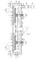
本開示の実施の形態に係る基板処理装置について説明する。図1、図2に示すように、この基板処理装置は、その内部が常圧雰囲気とされるローダーモジュール2を備えている。ローダーモジュール2には、ウエハWの搬送容器であるキャリアCを載置するための搬入出ポート1が例えば左右方向に3個並べて設置される。図1中符号21は、キャリアCの蓋と一緒に開閉されるドアである。 A substrate processing apparatus according to an embodiment of the present disclosure will be described. As shown in FIGS. 1 and 2, the substrate processing apparatus includes a loader module 2 in which the inside is at normal pressure. In the loader module 2, for example, three carry-in / out ports 1 for mounting a carrier C, which is a transfer container for the wafer W, are arranged side by side in the left-right direction.
ローダーモジュール2は、ウエハWを搬送するための搬送アーム5を備えている。搬送アーム5は、不図示の回転軸を介して接続された下段アーム部51、上段アーム部52及びウエハ保持部53を下方側からこの順で連結した多関節アームとして構成される。そして、ケース体54内に設けられた図示しないモータにより、多関節アーム全体が旋回あるいは進退するようになっている。この例では、搬送アーム5は、昇降機構55により、ガイドレール56に沿って、後述のロードロックモジュール3A、3Bの高さまで昇降するように構成される。 The loader module 2 includes a
図1に示すように、搬入出ポート1から見て、ローダーモジュール2の左側及び右側には、例えば平面視長方形状のロードロックモジュール3A、3Bが夫々設けられる。これらロードロックモジュール3A、3Bは、夫々の内部雰囲気を真空雰囲気と常圧雰囲気とを切り替えることができるようになっている。図1に示すように、ロードロックモジュール3A、3Bは、平面的に見て夫々ローダーモジュール2側に傾斜するように配置され、ローダーモジュール2は、平面視、搬入出ポート1側が長い略台形形状に構成される。 As shown in FIG. 1, for example,
ロードロックモジュール3A、3Bの長辺をなす側面は夫々ローダーモジュール2に接続され、当該側面には搬送口31が夫々形成される。また、ロードロックモジュール3A、3Bの短辺をなす側面は夫々後述する搬送室9に接続され、当該側面には搬送口33が夫々形成される。これら搬送口31、33は、夫々ゲートバルブ32、34により開閉される。
ロードロックモジュール3A、3Bの内部には、図2に示すように、ウエハWが載置される載置棚300が設けられる。例えば載置棚300は、ローダーモジュール2側から見て、2枚のウエハWが横方向に並び、かつ上下に間隔を開けて配置されるように構成される。The long sides of the
As shown in FIG. 2, a
載置棚300は、例えば図3に示すように、3本の支柱35と、各支柱35の長さ方向に間隔を置いて梁出すように設けられた爪部36とにより、ウエハWの周縁部を支持するように構成される。載置棚300の各部には、搬送口31を介して搬送アーム5との間、搬送口33を介して後述の基板搬送機構6との間で夫々ウエハWの受け渡しが行われる。このため、支柱35及び爪部36は、搬送アーム5及び基板搬送機構6に対して、互いに干渉しない状態でウエハWの受け渡しが行われるように、その形状や設置位置が設定される。 For example, as shown in FIG. 3, the
この例では、載置棚300が例えば上下に複数段設けられている。そして、ロードロックモジュール3Aの載置棚300が例えば未処理ウエハ用の載置棚、ロードロックモジュール3Bの載置棚300が、例えば処理済みウエハ用の載置棚として、夫々割り当てられる。以下明細書中では、搬送室9側から見て、手前側の載置棚を載置棚300Aと示し、奥側の載置棚を載置棚300Bと示す。 In this example, a plurality of mounting
図1に戻って、説明を続ける。搬送室9は前後方向に伸びる、平面視略長方形状に構成され、例えば底面部に形成された排気口90を介して真空排気部10に接続される。また、搬入出ポート1から見て搬送室9の左右には、例えば3台の処理モジュール4が夫々前後方向に並べて設けられる。さらに、搬送室9は、ロードロックモジュール3A、3B及び各処理モジュール4との間でウエハWの受け渡しを行うための基板搬送機構6を備えている。 Returning to FIG. 1, the description will be continued. The
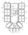
基板搬送機構6の説明に先立ち、処理モジュール4の一例について、例えばウエハWにプラズマALD(Atomic Layer Deposition)により成膜する成膜装置に適用した例を用いて説明する。この例における処理モジュール4は、真空雰囲気でウエハWに対して処理を行うモジュールである。図1及び図4に示すように、処理モジュール4は、平面視矩形の処理容器40を備え、処理容器40における搬送室9側の側壁には、ゲートバルブ42によって開閉されるウエハWの搬入出口41が形成される。図4中符号80は、処理容器40の底面に開口する排気口であり、圧力調整部82を備えた排気管81により真空ポンプ83に接続される。 Prior to the description of the substrate transfer mechanism 6, an example of the
処理容器40内には、搬入出口41から見て、手前から奥に向けて、処理部400A、400Bが列をなしてこの順で設けられ、これら処理部400A、400Bの列は搬入出口41から見て左右に並べて配置される。処理部400A及び400Bは、ウエハWを載置する載置台11A、11Bを備え、これにより平面的に見て、ウエハWは処理容器40内に2×2の行列状に合計4枚載置される。載置台11A、11Bは例えば扁平な円柱状に形成され、その内部にはウエハWを加熱するためのヒータ12が埋設される。 In the
載置台11A、11Bに載置されるウエハWは、ロードロックモジュール3A、3Bの載置棚300A、300Bに載置されるウエハWと、その配置間隔が互いに揃うように構成される。処理容器40内の4つの載置台11A、11Bは、支持アーム441により共通の支柱44を介して、処理容器40の下方に設けられた昇降部材43に接続される。こうして、4つの載置台11A、11Bが同時に、図4に実線で示す成膜処理を行う処理位置と、図4中鎖線で示すウエハWの受け渡し位置との間で昇降する。図4中の符号431は、処理容器40内を気密に保つためのシール部材である。 The wafers W mounted on the mounting tables 11A and 11B are configured such that the arrangement intervals between the wafers W mounted on the mounting
各載置台11A、11Bには、基板搬送機構6との間でウエハWの受け渡しを行なうための、例えば3本の昇降ピン46が昇降部材47により昇降自在に設けられる。図4及び図5中、符号45は昇降ピン46用の貫通孔、符号48はシール部材である。昇降ピン46は、図5に貫通孔45を示すように、後述する基板搬送機構6の第1のアーム65及び第2のアーム66がウエハWの受け渡しのために進入したときに、互いに干渉しない位置に設けられる。なお、図4では、図示の便宜上、昇降ピン46同士の間隔を狭く描いている。 On each of the mounting tables 11A and 11B, for example, three lifting
処理部400A及び400Bの上部側には、絶縁部材71を介して上部電極をなすガスシャワーヘッド7が各々設けられる。ガスシャワーヘッド7の下面は載置台11A、11Bに対向し、当該下面にはガス吐出孔72が多数、分散して配設される。ガスシャワーヘッド7には整合器73を介して高周波電源74が接続される。また、載置台11A、11B内には、図示しない下部電極が埋設されており、これら下部電極は接地電位に接続されている。図4中符号75はガス供給部であり、ガスシャワーヘッド7に、成膜される膜の原料となるTi(チタン)元素を含む原料ガスとして例えば四塩化チタン(TiCl4)を供給する。また、この原料ガスと反応させる反応ガスとして水素(H2)ガスとアルゴン(Ar)ガスとを含むガスを、原料ガスとは独立して供給する。On the upper side of the
処理モジュール4におけるウエハWの成膜処理について簡単に説明する。受け渡し位置に配置された4つの載置台11A、11BにウエハWを載置した後、ヒータ12によりウエハWを加熱すると共に、載置台11A、11Bが処理位置に移動する。次いで、ガスシャワーヘッド7から原料ガスを供給してウエハWの表面に吸着させる吸着段階を実施する。その後、ガスシャワーヘッド7から反応ガスを供給すると共に、高周波電源74からガスシャワーヘッド7と載置台11A、11B内の下部電極との間に高周波電力を供給する。これにより、反応ガスを容量結合によりプラズマ化させ、ウエハWの表面に吸着した原料ガスと反応させる反応段階を実施する。こうして、吸着段階と反応段階とを交互に繰り返して実施するプラズマALD法により、ウエハW表面にTi層を積層し、所定の膜厚を有するTi膜を成膜する。 The film forming process of the wafer W in the
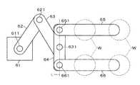
次に、基板搬送機構6について、図1、図6及び図7の模式図、図8の一部断面図を参照して説明する。基板搬送機構6は、基台61、第1の移動体62、第2の移動体63、回動体64を、下方側からこの順で連結した多関節アームとして構成される。基台61は、例えば搬送室9内において、前後方向の中央部において右寄りに設けられ、図示しない昇降部材により昇降自在に構成される。 Next, the substrate transport mechanism 6 will be described with reference to the schematic diagrams of FIGS. 1, 6, and 7, and a partial cross-sectional view of FIG. The substrate transfer mechanism 6 is configured as a multi-joint arm in which a
第1の移動体62及び第2の移動体63は、夫々水平に伸びる細長の板状体よりなる。第1の移動体62は、その基端側が基台61上の縦方向の回動軸611まわりに回動することにより、横方向に移動するように構成される。また、第2の移動体63は、その基端側が第1の移動体62の先端部上の縦方向の回動軸621まわりに回動することにより、横方向に移動するように構成される。 The first moving
後述の第1のアーム、第2のアームを支持する支持体である回動体64は、第2の移動体63の先端部に設けられた縦方向の回動軸631まわりに回動するように構成される。この回動体64の横方向に互いに離れた位置には、各々縦方向に第1の回動軸651及び第2の回動軸661が設けられる。この例では、回動体64の長さ方向の一端側に第1の回動軸651が設けられ、この第1の回動軸651には、第1のアーム65の基端側が接続される。また、回動体64の長さ方向の他端側には第2の回動軸661が設けられ、この第2の回動軸661には、第2のアーム66の基端側が接続される。 A rotating
第1のアーム65及び第2のアーム66は、夫々水平に伸びる細長のへら状に形成され、第1のアーム65及び第2のアーム66の長さは回動体64の長さよりも長くなるように設定される。これにより、第1のアーム65の基端側が第1の回動軸651まわりに回転するときには、その先端側が回動体64の外側を旋回するように構成される。また、第2のアーム66の基端側が第2の回動軸661まわりに回転するときには、その先端側が回動体64の外側を旋回するように構成される。回動体64を回動させる回動軸631は、平面的に見たときに、例えば第1の回動軸651と第2の回動軸661とを結ぶ直線L(以下「直線L」という)上に位置するように設けられる。さらに、この例では、回動軸631と第1の回動軸651との距離と、回動軸631と第2の回動軸661との距離が互いに揃うように設定される。 The
第1のアーム65は、ウエハWを支持する第1の基板支持領域をなすものであり、第2のアーム66は、第1のアーム65に支持されるウエハWとは別のウエハWを支持する第2の基板支持領域をなすものである。第1の基板支持領域及び第2の基板支持領域は、ウエハWの裏面に接してウエハWを支持する領域であり、夫々複数例えば2枚のウエハWを、第1のアーム65、第2のアーム66の長さ方向に沿って各々支持する領域として形成される。この例では、第1のアーム65、第2のアーム66には、互いに間隔を開けてウエハWの裏面が支持される。第1及び第2のアーム65、66は、夫々ウエハWの裏面の直径に沿った領域を支持する。第1及び第2のアーム65、66の幅はウエハWの直径よりも小さく形成され、例えば第1及び第2のアーム65、66の先端部に支持されるウエハWは、その中央部がアーム65、66の先端部に支持される。 The
既述のように、載置台11A、11Bと、ロードロックモジュール3A、3Bの載置棚300A、300Bと、は、互いに載置されるウエハWの配置間隔が揃うように構成されている。このため、処理モジュール4の処理部400A、ロードロックモジュール3A、3Bの載置棚300AのウエハWは、夫々第1のアーム65、第2のアーム66の基端寄りに支持される。また、処理モジュール4の処理部400B、ロードロックモジュール3A、3Bの載置棚300BのウエハWは、夫々第1のアーム65、第2のアーム66の先端部に支持される。 As described above, the mounting tables 11A and 11B and the mounting
第1及び第2のアーム65、66は、例えば図3に示すように、ロードロックモジュール3A、3Bに進入したときに、載置棚300A、300Bの各爪部36に干渉しない形状に設定される。さらに、例えば図5に示すように、処理モジュール4に進入したときに、処理部400A、400Bの各昇降ピン46に干渉しない形状に設定される。 For example, as shown in FIG. 3, the first and
このような基板搬送機構6において、例えば基台61上の回動軸611と第1の移動体62の回動軸621、この回動軸621と第2の移動体63の回動軸631は、夫々図示しないベルトにより接続される。そして、基台61内に設けられた図示しない進退用モータ及び旋回用モータにより、多関節アーム全体が旋回あるいは進退するように構成される。
また、第1の回動軸651と、第2の回動軸661は、互いに独立して駆動するように構成される。例えば第1の回動軸651については、基台61に当該回転軸651専用の図示しないモータが設けられる。そして、第1の移動体62、第2の移動体63、回動体64の内部に設けられた第1の回動軸651専用のベルト及びプーリに、モータの動力が伝達されて、第1の回動軸651が回動するように構成される。In such a substrate transport mechanism 6, for example, the
Further, the first
さらに、基板搬送機構6は、第2のアーム66が、第1のアーム65と干渉しないように、回動体64に対する第2のアーム66の向きに応じて、第2の回動軸661を昇降させる昇降機構を備える。例えば図7B、図8に示すように、第2の回動軸661の表面及び回動体64における回動軸661との接合部分にはネジが形成される。また、第1の回動軸651と同様に、基台61に第2の回動軸661専用の図示しないモータが設けられる。そして、第1の移動体62、第2の移動体63、回動体64の内部に、第2の回動軸661専用のベルト及びプーリが設けられる。 Further, the substrate transfer mechanism 6 raises and lowers the second
図8に、回動体64と第2のアーム66の接続部近傍の縦断面図を示す。図8中、符号662はベルト、663はプーリ、664、665はギアである。こうして、基台61に設けられた図示しないモータの動力がベルト662を介して、プーリ663に接続されたギア664に伝達され、これによりギア665を介して第2の回動軸661が回動する。そして、第2の回動軸661が回動したときには、ネジの作用により、第2のアーム66の回動体64に対する高さ位置が変化するように構成される。従って、この例における昇降機構は、第2の回動軸661及び回動体64に形成されたネジと、第2の回動軸661を回転させるためのモータ、プーリ、ギアにより構成される。 FIG. 8 is a vertical cross-sectional view of the vicinity of the connection between the
こうして、図6A、図6Bに示すように、直線Lに対して、第1及び第2のアーム65、66の長さ方向が夫々直交した姿勢では、第1及び第2の基板支持領域の高さが互いに揃うように構成される。このときの第1及び第2のアーム65、66は、第1のアーム65の向きと、第2のアーム66の向きとが同じであり、且つ回動軸631から第1及び第2の基板支持領域までの距離が互いに同じ姿勢である。ここでいう第1及び第2の基板支持領域の高さが揃うとは、設計上高さが同じであればよく、製造上の誤差があり、それによって各領域の高さが異なる場合も含む意味であり、例えば2mm以内の高さ位置の誤差は許容される。 In this manner, as shown in FIGS. 6A and 6B, when the length directions of the first and
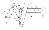
一方、図7A、図7Bに示すように、回動体64に対する第2のアーム66の向きが、前記長さ方向が直線Lに直交する姿勢から変化したときには、昇降機構により第2の回動軸661を上昇させる。上昇したときの第2の基板支持領域の高さは、第1のアーム65と第2のアーム66との干渉を防ぐために、第1の基板支持領域に支持されたウエハWの表面よりも、第2のアーム66の下面が高くなる高さ位置である。回動体64に対する第2のアーム66の向きと、第2の基板支持領域の高さ位置の変動量との対応関係は、適宜設定される。 On the other hand, as shown in FIGS. 7A and 7B, when the direction of the
このように、基板搬送機構6は、第1のアーム65と第2のアーム66とが、回動体64に対して互いに独立して、互いに干渉しないように回転自在に接続されるので、回動体64に対する向きを変えて、姿勢を変形することができる。
これにより、例えば処理モジュール4との間でウエハWの受け渡しを行なうときには、基板搬送機構5は、第1及び第2のアーム65、66の長さ方向が直線Lに対して夫々直交する受け渡し姿勢に設定される。そして、図1に示すように、処理モジュール4に第1のアーム65と第2のアーム66とが共に進入して、4枚のウエハWを一括して搬送するように構成される。As described above, the substrate transfer mechanism 6 is configured such that the
Thus, for example, when the wafer W is transferred to and from the
また、ロードロックモジュール3A、3Bとの間でウエハWの受け渡しを行なうときには、図9及び図10に示すように、直線Lに対して第1のアーム65の長さ方向及び第2のアーム66の長さ方向が各々傾く姿勢に設定される。そして、ロードロックモジュール3A、3Bに対して、第1のアーム65及び第2のアーム66が夫々別個に進入して、2枚のウエハWを一括して搬送するように構成される。 When the wafer W is transferred between the
さらに、図11に示すように、搬送室9内を移動するときには、直線Lに対して、第1のアーム65の長さ方向及び第2のアーム66の長さ方向が各々傾き、且つ第1のアーム65と第2のアーム66とが交差した搬送姿勢に構成される。このような第1及び第2のアーム65、66の姿勢変形は、第1及び第2の回動軸651、661用の夫々のモータ、回動軸611、621、631用の進退用及び旋回用モータへの、制御部100からの制御信号に基づいて行われる。ウエハWの搬送のスケジュールに対応して夫々のモータの駆動量が予め設定されており、第1及び第2のアーム65、66の移動、姿勢変形が制御され、ウエハWの受け渡しが行われる。 Further, as shown in FIG. 11, when moving in the
基板処理装置は、図1に示すように基板処理装置内におけるウエハWの搬送、処理モジュール4における成膜処理等のプロセス、ロードロックモジュール3A、3Bにおける雰囲気の切り替えを制御する制御部100を備えている。制御部100は例えば図示しないCPUと記憶部とを備えたコンピュータからなる。記憶部には処理モジュール4における成膜処理のレシピや、当該基板処理装置において、搬送アーム5及び基板搬送機構6によるウエハWの搬送を行うためのステップ(命令)群が組まれたプログラムが記録される。このプログラムは、例えばハードディスク、コンパクトディスク、マグネットオプティカルディスク、メモリカードなどの記憶媒体に格納され、そこからコンピュータにインストールされる。 As shown in FIG. 1, the substrate processing apparatus includes a
続いて、上述の実施の形態の作用について説明する。なお、以下、未処理のウエハWを未処理ウエハW0と示す。また、処理部400Aにて処理された処理済みウエハWをウエハWA、400Bにて処理された処理済みウエハWをウエハWBと示す。
図9に示すように、未処理ウエハW0を収容したキャリアCが搬入出ポート1上に載置されると、搬送アーム5は、キャリアCから未処理ウエハW0を順番に取出す。そして、ロードロックモジュール3Aのゲートバルブ32を開いて、ウエハ載置棚300A、300Bに夫々未処理ウエハW0を順次受け渡す。続いて、ゲートバルブ32を閉じ、ロードロックモジュール3A内の雰囲気を常圧雰囲気から真空雰囲気に切り替える。Next, the operation of the above embodiment will be described. Hereinafter, the unprocessed wafer W is referred to as an unprocessed wafer W0. The processed wafer W processed by the
As shown in FIG. 9, when the carrier C containing the unprocessed wafer W0 is placed on the loading / unloading port 1, the
次に、例えばロードロックモジュール3Aのゲートバルブ34を開き、基板搬送機構6における、第1及び第2のアーム65、66の向きを変え、第1のアーム65をロードロックモジュール3Aに進入させる。そして、第1のアーム65を、例えば最上段の載置棚300A、300Bに配置された未処理ウエハW0の下方に進入させた後、上昇させて、2枚の未処理ウエハW0を同時に掬い上げて保持する。次いで、未処理ウエハW0を保持した第1のアーム65を搬送室9に退出させる。 Next, for example, the
続いて、図10に示すように、基板搬送機構6における、第1及び第2のアーム65、66の向きを変え、第2のアーム66をロードロックモジュール3Aに進入させる。そして、第2のアーム66に、例えば上から2番目の載置棚300A、300Bに載置されている未処理ウエハW0を保持させた後、当該第2のアーム66を搬送室9に退出させ、ゲートバルブ34を閉じる。 Subsequently, as shown in FIG. 10, the directions of the first and
こうして、例えばロードロックモジュール3Aには第1のアーム65、第2のアーム66が順番に進入する。そして、ロードロックモジュール3A内の2枚の未処理ウエハW0を第1のアーム65及び第2のアーム66により、夫々一括して搬出する。一方、ロードロックモジュール3Aにおいては、未処理ウエハW0を払い出した後、ゲートバルブ34を閉じ、ロードロックモジュール3A内の雰囲気を常圧雰囲気に切り替える。 Thus, for example, the
搬送室9では、第1のアーム65及び第2のアーム66に各々2枚、計4枚の未処理ウエハW0を保持した基板搬送機構6は、図11に示すように、第1のアーム65及び第2のアーム66が交差する搬送姿勢に変形する。そして、この搬送姿勢の状態で、未処理ウエハW0が搬送される処理モジュール4に向けて第1及び第2の移動体62、63により移動する。次に、搬送対象である処理モジュール4のゲートバルブ42を開き、第1のアーム65及び第2のアーム66を処理モジュール4に対する受け渡し姿勢に変形する。 In the
次いで、図12に示すように、当該処理モジュール4に、受け渡し姿勢の第1及び第2のアーム65、66を共に進入させる。そして、第1のアーム65に保持した2枚のウエハW0を、処理モジュール4における搬入出口41から見て左側に並ぶ処理部400A、400Bの上方に位置させる。また、第2のアーム66に保持した2枚のウエハW0を、処理モジュール4における搬入出口41から見て右側に並ぶ処理部400A、400Bの上方に位置させる。 Next, as shown in FIG. 12, both the first and
続いて、4つの処理部400A、400Bの各々において昇降ピン46を上昇させて、第1及び第2のアーム65、66に夫々保持されたウエハW0を各々突き上げて受け取る。こうして、第1及び第2のアーム65に支持された基端寄りのウエハWと、先端部のウエハWを、夫々処理部400Aの載置台11Aと、処理部400Bの載置台11Bに各々載置する。その後、基板搬送機構6を搬送室9内に退出させ、ゲートバルブ42を閉じ、処理モジュール4において、既述の成膜処理を実行する。 Subsequently, the lifting pins 46 are raised in each of the four
このように、処理モジュール4に対してウエハWの搬送を行うときには、第1アーム65及び第2のアーム66は受け渡し姿勢であり、第1の基板支持領域と第2の基板支持領域の高さを揃えている。このような構成とするのは、搬入出口41に向かって見て、当該搬入出口41の左右の高さ位置及び幅を揃えるためである。仮に処理モジュール4への受け渡し時にアーム65、66の高さが異なるとすると、搬入出口41の左右で開口する高さ位置が異なったり、開口幅が異なることになる。 As described above, when the wafer W is transferred to the
処理モジュール4の処理容器40は金属により構成されて接地され、上部電極と下部電極との間の側壁はプラズマに接する導電路をなす。これにより、搬入出口41の高さ位置及び開口幅については当該プラズマの形成状態に影響を与えるおそれが有る。つまり、上記のように搬入出口41の高さ位置や開口幅が左右で異なると、プラズマの形成状態が処理容器内の左右で異なり、左側に載置されたウエハW、右側に載置されたウエハWとの間で処理の均一性が低下するおそれが有る。しかし、上記のように処理モジュール4へ受け渡す際にはアーム65、66の高さが揃えられるので、搬入出口41の左右の高さ及び幅も揃えることができる。その結果として、ウエハW間の処理の均一性が低下することを防ぐことができる。 The
その後、処理モジュール4にてウエハWの処理が終了すると、当該処理モジュール4におけるゲートバルブ42を開く。そして、4つの処理部400A、400Bに載置された各処理済みウエハWA、WB(WA、WBは図示せず)を昇降ピン46により突き上げる。次いで、第1のアーム65、第2のアーム66を処理モジュール4に対する受け渡し姿勢に変形して、これら第1及び第2のアーム65、66を共に進入させる。この後、基板搬送機構6と昇降ピンとの協働作用により、第1及び第2のアーム65、66の夫々に対して、基端寄りにウエハWAを受け渡すと共に、先端部にウエハWBを受け渡す。 Thereafter, when the processing of the wafer W is completed in the
続いて、処理済みのウエハWA、WBを夫々支持した第1のアーム65及び第2のアーム66が搬送室9に退出した後、ゲートバルブ42を閉じ、基板搬送機構6は、既述の搬送姿勢に変形する。この搬送姿勢の状態で、ロードロックモジュール3Bに向けて移動するが、ロードロックモジュール3Bにおいては、真空雰囲気に切り替えた状態で待機している。そして、ロードロックモジュール3Bのゲートバルブ34を開き、2枚の処理済みウエハWA、WBを保持した第1のアーム65を載置棚300A、300Bに受け渡すために、ロードロックモジュール3B内に進入させる。 Subsequently, after the
次いで、第1のアーム65を下降させ、当該アーム65に保持されているウエハWA、WBを例えば最上段の載置棚300A、300Bに夫々受け渡す。こうして、第1のアーム65に保持されている2枚のウエハWを一括してロードロックモジュール3Bの載置棚300A、300Bに受け渡す。
同様に、2枚の処理済みウエハWA、WBを保持した第2のアーム66をロードロックモジュール3B内に進入する。そして、第2のアーム66に保持されている2枚のウエハWを一括してロードロックモジュール3Bの例えば上から2番目の載置棚300A、300Bに受け渡す。この後、ロードロックモジュール3Bのゲートバルブ34を閉じて、当モジュール内の雰囲気を常圧雰囲気に切り替える。続いて、ゲートバルブ32を開いて、処理済みのウエハWを搬送アーム5により、例えば元のキャリアCに戻す。Next, the
Similarly, the
上述の実施形態によれば、回動体64に、第1の回動軸651により回転自在に第1のアーム65を接続すると共に、第2の回動軸661により回転自在に第2のアーム66を接続する。また、第2のアーム66が回転するときに、第1のアーム65と干渉しないように、第2の回動軸661を昇降させている。このため、回動体64に対する第1のアーム65及び第2のアーム66の向きを、互いに独立して、互いに干渉せずに変えることができる。これにより、ウエハWの搬送先のモジュールにおける当該ウエハWの配置及びモジュール間でのウエハWの搬送態様について自由度を高くすることができる。 According to the above-described embodiment, the
第1の基板支持領域及び第2の基板支持領域は、複数例えば2枚のウエハWを、第1のアーム65、第2のアーム66の長さ方向に沿って各々支持する領域として構成される。このため、2本のアーム65、66を用いるときには、4枚のウエハWを一括して搬送でき、1本のアーム65(66)を用いるときには、2枚のウエハWを一括して搬送できる。これにより、この例では、1台の基板搬送機構6により、4枚のウエハWの一括搬送と、2枚のウエハWの一括搬送に対応することができる。このため、モジュール間においてウエハWの配置が異なっていても、互いにウエハWの受け渡しを行うことができて、モジュールにおけるウエハWの配置やモジュール間でのウエハWの搬送態様についての自由度が高い。 The first substrate support region and the second substrate support region are configured as regions that respectively support a plurality of, for example, two wafers W along the length direction of the
例えばウエハWを4枚一括して搬送する基板搬送機構を用いる場合には、ウエハWの搬送に要する時間を短縮できるため、スループットを高め、生産性の向上に寄与することができる。但し、全てのモジュールを4枚のウエハWが平面的に見て並んで載置される構成にする必要があるため、装置の専有面積が大きくなるという懸念がある。一方、ウエハWを2枚一括して搬送する基板搬送機構を用いる場合には、4枚のウエハWが載置されるモジュールと、2枚のウエハWが載置されるモジュールとに対してウエハWを搬送できる。このため、基板処理装置に2枚のウエハWが平面的に見て並んで載置されるモジュールも組み込むことができ、装置の小型化を図ることができる。但し、4枚のウエハWが載置されるモジュールに対しては、ウエハWを2枚ずつ搬送するために、搬送に要する時間が長くなってしまう。 For example, when a substrate transfer mechanism that transfers four wafers W at once is used, the time required to transfer the wafers W can be reduced, so that the throughput can be increased and the productivity can be improved. However, since all the modules need to have a configuration in which four wafers W are placed side by side in a plan view, there is a concern that the occupied area of the apparatus becomes large. On the other hand, when a substrate transfer mechanism that transfers two wafers W at once is used, a module on which four wafers W are mounted and a module on which two wafers W are mounted W can be transported. Therefore, a module in which two wafers W are placed side by side in a plan view can be incorporated in the substrate processing apparatus, and the apparatus can be downsized. However, for a module on which four wafers W are mounted, the time required for the transfer is long because the wafers W are transferred two by two.
従って、1台の基板搬送機構6により、モジュールに対して、2本のアーム65、66を用いた4枚のウエハWの一括搬送と、1本のアーム65(66)のみを用いた2枚のウエハWの一括搬送ができる構成はメリットが多い。つまり、処理モジュール4は4枚のウエハWが平面的に見て並んで載置される構成とし、4枚のウエハWを一括して搬送することにより、スループットを高めることができる。一方、ロードロックモジュール3A、3Bは2枚のウエハWが平面的に見て並んで載置される構成とし、2枚のウエハWを一括して搬送することにより、4枚のウエハWを載置する構成に対して装置の専有面積を縮小することができる。このように、1台の基板処理装置に、4枚のウエハWが載置されるモジュールと、2枚のウエハWが載置されるモジュールと、を組み込むことができる。このため、モジュールにおけるウエハWの配置の自由度が高く、装置構成の自由度が高くなる。 Therefore, one substrate transfer mechanism 6 collectively transfers four wafers W using two
また、基板搬送機構6は回動体64に対してアーム55、56が互いに独立して回動できる。それによって、上記のようにロードロックモジュール3A、3Bを大気搬送室に対して平面視斜めの配置として、アーム55、56が当該ロードロックモジュール3A、3Bに対してウエハWを受け渡すことができる。即ち、ロードロックモジュール3A、3Bを搬送室9の手前に配置し、例えば左右方向に搬送室2を配置するよりも装置の左右の幅の縮小化を図ることができる。つまり、装置のフットプリントを抑制することができる。 Further, in the substrate transport mechanism 6, the
さらに、第1のアーム65及び第2のアーム66を互いに独立して、かつ互いに干渉しないように回動体64に対する向きを変えることができるので、第1のアーム65と第2のアーム66とが交差する姿勢を形成することができる。このため、旋回半径が縮小され、この姿勢で搬送室9内を移動することにより、搬送室9の小型化を図ることができ、この点からも基板処理装置の小型化に寄与することができる。さらにまた、第1のアーム65と第2のアームとが交差する姿勢により形状を小さくすることによって、慣性質量を小さくすることができる。これにより、加速及び減速がしやすくなるため、第1及び第2の移動体62、63による旋回動作を速やかに行うことができ、有利である。 Further, since the
続いて、本開示の基板搬送機構6を用いた他の搬送例について、図13を参照して説明する。この例は、搬送室9に接続された一の処理モジュール4Aにて処理を行ったウエハWを、基板搬送機構6により他の処理モジュール4Bに搬送し、当該他の処理モジュール4Bにおいてさらに処理を行う場合に適用される。なお、処理モジュール4A、4Bは、説明の便宜上用いた符号であり、処理モジュール4Bの図示は省略する。また、図13に示す第1及び第2のアーム65、66の形態は、図示の便宜上のものであり、実際の搬送時のアーム65、66の形態とは異なっている。ここでは、ウエハWを支持していないアームを空のアームと表現する。また、第1のウエハW1が処理モジュール4Aにて処理が行われた処理済みウエハW1、第2のウエハW2はロードロックモジュール3Aから受け取られた未処理のウエハWとして説明する。 Subsequently, another transfer example using the substrate transfer mechanism 6 of the present disclosure will be described with reference to FIG. In this example, the wafer W processed in one
先ず、図13(S1)に示すように、処理モジュール4Aに収納された第1の基板である第1のウエハW1を受け取るために、第1のアーム65が当該処理モジュール4Aに進入するステップを実行する。つまり、空の第1のアーム65を処理モジュール4Aに進入させ、搬入出口から見て左側の載置台11A、11BからウエハW1を受け取る。そして、第1のウエハW1を支持した第1のアーム65が当該処理モジュール4Aから退出するステップを行う。 First, as shown in FIG. 13 (S1), in order to receive the first wafer W1, which is the first substrate housed in the
その後、図13(S2)に示すように、第2の基板である第2のウエハW2を支持した第2のアーム66が、前記処理モジュール4Aに当該ウエハW2を搬送するために、当該処理モジュール4Aに進入するステップを実行する。そして、搬入出口から見て左側の載置台11A、11Bに第2のウエハW2を受け渡した後、空の第2のアーム66が処理モジュール4Aから退出する。 Thereafter, as shown in FIG. 13 (S2), the
続いて、第1のウエハW1を支持する第1のアーム65を、例えば次工程の処理を行なう処理モジュール4Bに搬送し、第1のアーム65が処理モジュール4Bに進入して、載置台11A、11BにウエハW1を受け渡す。この後、空の第1のアーム65は処理モジュール4Bから退出する。一方、空の第2のアーム66は、ロードロックモジュール3Aに進入し、未処理のウエハW2を受け取って支持する。 Subsequently, the
次いで、図13(S3)に示すように、空の第1のアーム65を処理モジュール4Aに進入して、処理モジュール4Aにおける搬入出口から見て右側の載置台11A、11Bから第1のウエハW1を受け取るステップを実行する。そして、第1のウエハW1を支持した第1のアーム65が当該処理モジュール4Aから退出するステップを行う。その後、図13(S4)に示すように、第2の基板である第2のウエハW2を支持した第2のアーム66を処理モジュール4Aに進入するステップを実行し、搬入出口から見て右側の載置台11A、11Bに第2のウエハW2を受け渡す。そして、空の第2のアーム66が処理モジュール4Aから退出する。これらのステップは、制御部100から出力される制御信号に基づいて実行される。 Next, as shown in FIG. 13 (S3), the empty
こうして、処理モジュール4Aの4つの載置台11A、11Bには、未処理のウエハW2が載置され、所定の処理が実行される。一方、処理モジュール4Bについても、既述の搬送動作を繰り返すことにおり、4つの載置台11A、11BにウエハW1が載置され、次工程の処理が実施される。
このように、本開示の基板搬送機構6を用いることにより、処理モジュール4に対するウエハWの搬送を4枚一括のみならず、2枚一括で行うことができるので、搬送の自由度が高い。Thus, the unprocessed wafer W2 is mounted on the four mounting tables 11A and 11B of the
As described above, by using the substrate transfer mechanism 6 of the present disclosure, the transfer of the wafer W to the
以上において、回動体64を縦軸回りに回動させる回動軸631は、必ずしも第1の回動軸651及び第2の回動軸661と横方向に離れている必要はない。例えば回動軸631と第1の回動軸651を縦方向に重ねて、例えば共通の構成にしてもよいし、回動軸631と第2の回動軸661を縦方向に重ねて、例えば共通の構成にしてもよい。また、第2の回動軸661の昇降機構としては、回動体64に第2の回動軸661を回転させるモータを設け、ネジが形成された第2の回動軸661を回転させることにより、昇降させるようにしてもよい。 In the above description, the
さらに、第2の回動軸661は、ネジを利用して回動軸を昇降させることには限られない。例えば回動体64に、第2の回動軸661を回動させるモータと、当該モータが設けられるアクチュエータからなる昇降機構と、を設け、第2の回動軸661及びモータが昇降機構により昇降するものであってもよい。なお、各例においてモータにより回動軸を回動させると説明しているが、このモータによる回動は図8で説明したようにプーリ及びベルトを介してモータの回動よりも低い速度で回動軸を回動させてもよい。その他にギアを介して回動軸をモータの回動よりも低い速度となるように回動させてもよいし、モータに直接回動軸を接続して、当該回動軸を回動させてもよい。 Further, the second
また、第2のアーム66と第1のアーム65とが干渉しないように、各アームの長さ方向が直線L(図6A参照)に直交する姿勢から変化したときには、第2の回動軸661が下降するように構成してもよい。さらに、第2の回動軸661を昇降させる昇降機構と、第1の回転軸651を昇降させる昇降機構と、を両方設けるようにしてもよい。そして、回動体64に対する第2のアーム66の向きに応じて、第1の回転軸651、第2の回動軸661の一方が上昇し、他方が下降するように構成してもよい。また、上述の基板搬送機構は、第1の移動体62及び第2の移動体63を備える構成としたが、一つの移動体に回動体が接続される構成であってもよい。 When the length direction of each arm changes from a posture orthogonal to the straight line L (see FIG. 6A) so that the
本開示の基板処理装置は例示であり、2枚の基板が搬送室から見て手前側と奥側に並んで配置される構成の処理モジュールを組み込み、当該処理モジュールに基板搬送機構より、2枚の基板を一括して受け渡すようにとしてもよい。また、ロードロックモジュールを、4枚の基板が平面的に見て2×2の行列状に載置される構成とし、このロードロックモジュールに対して、基板搬送機構により4枚の基板を一括して受け渡すようにしてもよい。さらに、第1のアーム及び第2のアームの一方において、その先端部に基板を支持し、複数の基板が配置される処理モジュール又は1枚の基板のみが配置される処理モジュールに、1枚の基板を受け渡すようにしてもよい。さらにまた、処理モジュールにおいて、真空雰囲気にて基板に実施される処理は、成膜処理に限らず、エッチング処理やアッシング処理であってもよい。 The substrate processing apparatus of the present disclosure is an example, and incorporates a processing module having a configuration in which two substrates are arranged side by side on the front side and the rear side when viewed from the transfer chamber, and the substrate transfer mechanism includes two substrates. May be delivered collectively. Further, the load lock module has a configuration in which four substrates are placed in a 2 × 2 matrix when viewed in a plan view, and the four substrates are collectively mounted on the load lock module by a substrate transport mechanism. May be delivered. Further, in one of the first arm and the second arm, a substrate is supported at the tip thereof, and one processing module in which a plurality of substrates are disposed or a processing module in which only one substrate is disposed is provided. The substrate may be delivered. Furthermore, in the processing module, the processing performed on the substrate in the vacuum atmosphere is not limited to the film forming processing, but may be an etching processing or an ashing processing.
今回開示された実施形態は全ての点で例示であって制限的なものではないと考えられるべきである。上記の実施形態は、添付の請求の範囲及びその主旨を逸脱することなく、様々な形態で省略、置換、変更されてもよい。 The embodiments disclosed this time are to be considered in all respects as illustrative and not restrictive. The above embodiments may be omitted, replaced, or modified in various forms without departing from the scope of the appended claims and the spirit thereof.
62 第1の移動体
63 第2移動体
64 回動体
65 第1のアーム
66 第2のアーム
651 第1の回動軸
661 第2の回動軸62 first moving
Claims (9)
Translated fromJapanese前記移動体に縦軸回りに回動するように設けられた支持体と、
前記支持体の横方向に互いに離れた位置に各々縦方向に設けられた第1の回動軸及び第2の回動軸と、
前記第1の回動軸に基端側が接続され、先端側が前記支持体の外側を旋回すると共に前記基板を支持する第1の基板支持領域をなす第1のアームと、
前記第2の回動軸に基端側が接続され、先端側が前記支持体の外側を旋回すると共に前記第1のアームに支持される前記基板とは別の基板を支持する第2の基板支持領域をなす第2のアームと、
前記第1のアームと前記第2のアームとが干渉しないように、前記支持体に対する当該第2のアームの向きに応じて前記第2の回動軸を昇降させる昇降機構と、
を備える基板搬送機構。A moving body that moves sideways,
A support provided on the moving body so as to rotate around a vertical axis,
A first rotation axis and a second rotation axis each provided in the vertical direction at positions spaced apart from each other in the horizontal direction of the support;
A first arm having a base end connected to the first rotation shaft, a front end pivoting around the outside of the support, and forming a first substrate support region for supporting the substrate;
A second substrate support area connected to the second pivot axis, the distal end pivoting outside the support, and supporting a substrate different from the substrate supported by the first arm. A second arm,
An elevating mechanism that elevates and lowers the second rotation axis in accordance with the direction of the second arm with respect to the support so that the first arm and the second arm do not interfere with each other;
A substrate transport mechanism comprising:
前記搬送室に接続され、真空雰囲気で前記基板に処理を行う処理モジュールと、
前記搬送室に接続されるロードロックモジュールと、
前記ロードロックモジュールと前記処理モジュールとの間で前記基板を搬送するために前記搬送室に設けられる請求項1ないし4のいずれか一つに記載の基板搬送機構と、
前記基板を格納した搬送容器が載置され、当該搬送容器と前記ロードロックモジュールとの間で前記基板を搬送するローダーモジュールと、
を備える基板処理装置。A transfer chamber in a vacuum atmosphere,
A processing module connected to the transfer chamber and performing processing on the substrate in a vacuum atmosphere;
A load lock module connected to the transfer chamber,
The substrate transfer mechanism according to any one of claims 1 to 4, wherein the substrate transfer mechanism is provided in the transfer chamber to transfer the substrate between the load lock module and the processing module.
A transport container storing the substrate is placed thereon, and a loader module that transports the substrate between the transport container and the load lock module;
A substrate processing apparatus comprising:
前記処理モジュールには前記第1のアーム及び第2のアームが共に進入して基板の搬送が行われるように制御信号を出力する制御部が設けられる請求項6記載の基板処理装置。The first arm and the second arm sequentially enter the load lock module,
7. The substrate processing apparatus according to claim 6, wherein the processing module is provided with a control unit that outputs a control signal so that the first arm and the second arm both enter and carry the substrate.
次いで前記基板を支持した第1のアームが当該処理モジュールから退出するステップと、
その後、第2の基板を支持した第2のアームが前記処理モジュールに基板を搬送するために当該処理モジュールに進入するステップと、
が行われるように制御信号を出力する制御部が設けられる請求項6記載の基板処理装置。A first arm entering the processing module to receive a first substrate stored in the processing module;
Then, the first arm supporting the substrate exits from the processing module;
Then, a second arm supporting a second substrate enters the processing module to transfer the substrate to the processing module;
7. The substrate processing apparatus according to claim 6, further comprising a control unit that outputs a control signal so that the control is performed.
前記移動体に設けられた支持体を縦軸回りに回動させる工程と、
前記支持体の横方向に互いに離れた位置に各々縦方向に設けられた第1の回動軸及び第2の回動軸を回動させる工程と、
前記第1の回動軸に基端側が接続される第1のアームについて、前記基板を支持する第1の基板支持領域をなす先端側を、前記支持体の外側を旋回させる工程と、
前記第2の回動軸に基端側が接続される第2のアームについて、前記第1のアームに支持される前記基板とは別の基板を支持する第2の基板支持領域をなす先端側を、前記支持体の外側を旋回させる工程と、
前記第1のアームと前記第2のアームとが干渉しないように、前記支持体に対する当該第2のアームの向きに応じて前記第2の回動軸を昇降させる工程と、
を備える基板搬送方法。Moving the moving body in the lateral direction;
Rotating the support provided on the moving body around a vertical axis,
Rotating a first rotation axis and a second rotation axis provided in a vertical direction at positions spaced apart from each other in the horizontal direction of the support;
For a first arm having a base end connected to the first rotation axis, a step of turning the tip side forming a first substrate support region for supporting the substrate, outside the support,
With respect to the second arm whose base end is connected to the second rotation shaft, the front end forming a second substrate support region for supporting a substrate different from the substrate supported by the first arm is referred to as a second arm. Turning the outside of the support,
Raising and lowering the second rotation axis according to the orientation of the second arm with respect to the support so that the first arm and the second arm do not interfere with each other;
A substrate transport method comprising:
Priority Applications (3)
| Application Number | Priority Date | Filing Date | Title |
|---|---|---|---|
| JP2018164629AJP7225613B2 (en) | 2018-09-03 | 2018-09-03 | SUBSTRATE TRANSFER MECHANISM, SUBSTRATE PROCESSING APPARATUS AND SUBSTRATE TRANSFER METHOD |
| US16/554,433US11404299B2 (en) | 2018-09-03 | 2019-08-28 | Substrate transfer mechanism, substrate processing apparatus, and substrate processing method |
| KR1020190107552AKR102244354B1 (en) | 2018-09-03 | 2019-08-30 | Substrate transfer mechanism, substrate processing apparatus, and substrate processing method |
Applications Claiming Priority (1)
| Application Number | Priority Date | Filing Date | Title |
|---|---|---|---|
| JP2018164629AJP7225613B2 (en) | 2018-09-03 | 2018-09-03 | SUBSTRATE TRANSFER MECHANISM, SUBSTRATE PROCESSING APPARATUS AND SUBSTRATE TRANSFER METHOD |
Publications (2)
| Publication Number | Publication Date |
|---|---|
| JP2020038880Atrue JP2020038880A (en) | 2020-03-12 |
| JP7225613B2 JP7225613B2 (en) | 2023-02-21 |
Family
ID=69640056
Family Applications (1)
| Application Number | Title | Priority Date | Filing Date |
|---|---|---|---|
| JP2018164629AActiveJP7225613B2 (en) | 2018-09-03 | 2018-09-03 | SUBSTRATE TRANSFER MECHANISM, SUBSTRATE PROCESSING APPARATUS AND SUBSTRATE TRANSFER METHOD |
Country Status (3)
| Country | Link |
|---|---|
| US (1) | US11404299B2 (en) |
| JP (1) | JP7225613B2 (en) |
| KR (1) | KR102244354B1 (en) |
Cited By (3)
| Publication number | Priority date | Publication date | Assignee | Title |
|---|---|---|---|---|
| JP2021180306A (en)* | 2020-05-12 | 2021-11-18 | エーエスエム・アイピー・ホールディング・ベー・フェー | High throughput multi-chamber substrate processing system |
| JP2023535578A (en)* | 2020-09-02 | 2023-08-18 | アプライド マテリアルズ インコーポレイテッド | Systems and methods for incorporating loadlocks into factory interface footprint spaces |
| KR20230152116A (en)* | 2021-03-01 | 2023-11-02 | 어플라이드 머티어리얼스, 인코포레이티드 | Vacuum robotic device for variable pitch approach |
Families Citing this family (7)
| Publication number | Priority date | Publication date | Assignee | Title |
|---|---|---|---|---|
| JP7183635B2 (en)* | 2018-08-31 | 2022-12-06 | 東京エレクトロン株式会社 | SUBSTRATE TRANSFER MECHANISM, SUBSTRATE PROCESSING APPARATUS AND SUBSTRATE TRANSFER METHOD |
| US11721564B2 (en)* | 2019-04-08 | 2023-08-08 | Tokyo Electron Limited | Substrate processing system and substrate transfer apparatus and method |
| US11574826B2 (en)* | 2019-07-12 | 2023-02-07 | Applied Materials, Inc. | High-density substrate processing systems and methods |
| CN114730728A (en)* | 2019-11-01 | 2022-07-08 | 朗姆研究公司 | Wafer Handling Robot with Gravity Field Sensor |
| KR102833850B1 (en)* | 2020-03-24 | 2025-07-14 | 주식회사 원익아이피에스 | Transfer Robot and Substrate Processing apparatus having the same |
| KR20230037990A (en) | 2021-09-10 | 2023-03-17 | 삼성전자주식회사 | Wafer processing device comprising efem and method for processing wafer |
| JP7408853B1 (en)* | 2023-01-26 | 2024-01-05 | 東京エレクトロン株式会社 | Substrate processing equipment |
Citations (6)
| Publication number | Priority date | Publication date | Assignee | Title |
|---|---|---|---|---|
| JP2004235538A (en)* | 2003-01-31 | 2004-08-19 | Tokyo Electron Ltd | Conveying device, vacuum processing device, and o-ring |
| JP2006294786A (en)* | 2005-04-08 | 2006-10-26 | Ulvac Japan Ltd | Substrate conveying system |
| KR20080039775A (en)* | 2006-11-01 | 2008-05-07 | 주식회사 아이피에스 | Wafer Transfer Robot, Wafer Processing System and Wafer Processing Method |
| JP2008135630A (en)* | 2006-11-29 | 2008-06-12 | Jel:Kk | Substrate conveying device |
| JP2013131543A (en)* | 2011-12-20 | 2013-07-04 | Tokyo Electron Ltd | Substrate processing apparatus |
| US20170040204A1 (en)* | 2015-08-07 | 2017-02-09 | Asm Ip Holdings B.V. | Substrate processing apparatus |
Family Cites Families (9)
| Publication number | Priority date | Publication date | Assignee | Title |
|---|---|---|---|---|
| US8731706B2 (en)* | 2008-09-12 | 2014-05-20 | Hitachi High-Technologies Corporation | Vacuum processing apparatus |
| JP6079200B2 (en)* | 2012-05-16 | 2017-02-15 | 東京エレクトロン株式会社 | Cooling mechanism and processing system |
| TWI625814B (en)* | 2012-07-27 | 2018-06-01 | 荏原製作所股份有限公司 | Workpiece transport device |
| JP5990359B2 (en) | 2012-10-04 | 2016-09-14 | 平田機工株式会社 | Loading / unloading robot |
| JP6438189B2 (en)* | 2013-10-01 | 2018-12-12 | 川崎重工業株式会社 | Robot and robot control method |
| JP6314157B2 (en)* | 2013-12-26 | 2018-04-18 | 川崎重工業株式会社 | End effector and substrate transfer robot |
| TWI709163B (en)* | 2017-09-26 | 2020-11-01 | 日商國際電氣股份有限公司 | Substrate processing device, semiconductor device manufacturing method and program |
| JP7090469B2 (en)* | 2018-05-15 | 2022-06-24 | 東京エレクトロン株式会社 | Board processing equipment |
| JP7183635B2 (en)* | 2018-08-31 | 2022-12-06 | 東京エレクトロン株式会社 | SUBSTRATE TRANSFER MECHANISM, SUBSTRATE PROCESSING APPARATUS AND SUBSTRATE TRANSFER METHOD |
- 2018
- 2018-09-03JPJP2018164629Apatent/JP7225613B2/enactiveActive
- 2019
- 2019-08-28USUS16/554,433patent/US11404299B2/enactiveActive
- 2019-08-30KRKR1020190107552Apatent/KR102244354B1/enactiveActive
Patent Citations (6)
| Publication number | Priority date | Publication date | Assignee | Title |
|---|---|---|---|---|
| JP2004235538A (en)* | 2003-01-31 | 2004-08-19 | Tokyo Electron Ltd | Conveying device, vacuum processing device, and o-ring |
| JP2006294786A (en)* | 2005-04-08 | 2006-10-26 | Ulvac Japan Ltd | Substrate conveying system |
| KR20080039775A (en)* | 2006-11-01 | 2008-05-07 | 주식회사 아이피에스 | Wafer Transfer Robot, Wafer Processing System and Wafer Processing Method |
| JP2008135630A (en)* | 2006-11-29 | 2008-06-12 | Jel:Kk | Substrate conveying device |
| JP2013131543A (en)* | 2011-12-20 | 2013-07-04 | Tokyo Electron Ltd | Substrate processing apparatus |
| US20170040204A1 (en)* | 2015-08-07 | 2017-02-09 | Asm Ip Holdings B.V. | Substrate processing apparatus |
Cited By (7)
| Publication number | Priority date | Publication date | Assignee | Title |
|---|---|---|---|---|
| JP2021180306A (en)* | 2020-05-12 | 2021-11-18 | エーエスエム・アイピー・ホールディング・ベー・フェー | High throughput multi-chamber substrate processing system |
| JP2023535578A (en)* | 2020-09-02 | 2023-08-18 | アプライド マテリアルズ インコーポレイテッド | Systems and methods for incorporating loadlocks into factory interface footprint spaces |
| JP7372500B2 (en) | 2020-09-02 | 2023-10-31 | アプライド マテリアルズ インコーポレイテッド | Systems and methods for incorporating loadlocks into a factory interface footprint space |
| KR20230152116A (en)* | 2021-03-01 | 2023-11-02 | 어플라이드 머티어리얼스, 인코포레이티드 | Vacuum robotic device for variable pitch approach |
| JP2024509519A (en)* | 2021-03-01 | 2024-03-04 | アプライド マテリアルズ インコーポレイテッド | Vacuum robot device for variable pitch access |
| JP7682288B2 (en) | 2021-03-01 | 2025-05-23 | アプライド マテリアルズ インコーポレイテッド | Variable pitch access vacuum robot device |
| KR102834294B1 (en)* | 2021-03-01 | 2025-07-14 | 어플라이드 머티어리얼스, 인코포레이티드 | Vacuum robotic device for variable pitch approach |
Also Published As
| Publication number | Publication date |
|---|---|
| US20200075377A1 (en) | 2020-03-05 |
| JP7225613B2 (en) | 2023-02-21 |
| KR102244354B1 (en) | 2021-04-23 |
| US11404299B2 (en) | 2022-08-02 |
| KR20200026745A (en) | 2020-03-11 |
Similar Documents
| Publication | Publication Date | Title |
|---|---|---|
| JP7225613B2 (en) | SUBSTRATE TRANSFER MECHANISM, SUBSTRATE PROCESSING APPARATUS AND SUBSTRATE TRANSFER METHOD | |
| US6331095B1 (en) | Transportation system and processing apparatus employing the transportation system | |
| JP4912253B2 (en) | Substrate transport apparatus, substrate processing apparatus, and substrate transport method | |
| US9443749B2 (en) | Vacuum processing apparatus | |
| US6746195B2 (en) | Semiconductor transfer and manufacturing apparatus | |
| CN100573820C (en) | Substrate board treatment | |
| JP7210960B2 (en) | Vacuum processing apparatus and substrate transfer method | |
| KR102355575B1 (en) | vacuum processing unit | |
| US10872798B2 (en) | Substrate transfer mechanism, substrate processing apparatus, and substrate transfer method | |
| US20150243490A1 (en) | Substrate processing apparatus and substrate processing method | |
| JP6045869B2 (en) | Substrate processing apparatus and substrate processing method | |
| JP2008166369A (en) | Substrate processing apparatus and substrate processing method | |
| JP2010045214A (en) | Substrate carrying device and substrate treatment device having the same | |
| JP2017199735A (en) | Substrate exchange system, substrate exchange method and memorizing medium | |
| TW201212147A (en) | Substrate processing apparatus and substrate processing system | |
| JP2013009007A (en) | Substrate transfer method in substrate processing apparatus | |
| JP2004006665A (en) | Vacuum processing device | |
| CN113451186B (en) | Transfer robot and substrate processing system including the same | |
| KR101383248B1 (en) | High speed substrate processing system | |
| KR20070015759A (en) | Flat panel display device manufacturing device | |
| JPH07297154A (en) | Substrate carrying system | |
| KR20030010088A (en) | Semiconductor manufacturing equipment for ashing process | |
| JP2001267391A (en) | Cassette storing equipment and substrate cleaning system | |
| KR20050061912A (en) | Cluster which comprises robot transferring a substrate at a straight line locus |
Legal Events
| Date | Code | Title | Description |
|---|---|---|---|
| A621 | Written request for application examination | Free format text:JAPANESE INTERMEDIATE CODE: A621 Effective date:20210520 | |
| A977 | Report on retrieval | Free format text:JAPANESE INTERMEDIATE CODE: A971007 Effective date:20220513 | |
| A131 | Notification of reasons for refusal | Free format text:JAPANESE INTERMEDIATE CODE: A131 Effective date:20220531 | |
| A521 | Request for written amendment filed | Free format text:JAPANESE INTERMEDIATE CODE: A523 Effective date:20220721 | |
| A131 | Notification of reasons for refusal | Free format text:JAPANESE INTERMEDIATE CODE: A131 Effective date:20221115 | |
| A521 | Request for written amendment filed | Free format text:JAPANESE INTERMEDIATE CODE: A523 Effective date:20221213 | |
| TRDD | Decision of grant or rejection written | ||
| A01 | Written decision to grant a patent or to grant a registration (utility model) | Free format text:JAPANESE INTERMEDIATE CODE: A01 Effective date:20230110 | |
| A61 | First payment of annual fees (during grant procedure) | Free format text:JAPANESE INTERMEDIATE CODE: A61 Effective date:20230123 | |
| R150 | Certificate of patent or registration of utility model | Ref document number:7225613 Country of ref document:JP Free format text:JAPANESE INTERMEDIATE CODE: R150 |