JP2020038378A - Semiconductor device - Google Patents
Semiconductor deviceDownload PDFInfo
- Publication number
- JP2020038378A JP2020038378AJP2019197427AJP2019197427AJP2020038378AJP 2020038378 AJP2020038378 AJP 2020038378AJP 2019197427 AJP2019197427 AJP 2019197427AJP 2019197427 AJP2019197427 AJP 2019197427AJP 2020038378 AJP2020038378 AJP 2020038378A
- Authority
- JP
- Japan
- Prior art keywords
- transistor
- electrode
- layer
- electrically connected
- input
- Prior art date
- Legal status (The legal status is an assumption and is not a legal conclusion. Google has not performed a legal analysis and makes no representation as to the accuracy of the status listed.)
- Granted
Links
Images


Classifications
- G—PHYSICS
- G06—COMPUTING OR CALCULATING; COUNTING
- G06F—ELECTRIC DIGITAL DATA PROCESSING
- G06F3/00—Input arrangements for transferring data to be processed into a form capable of being handled by the computer; Output arrangements for transferring data from processing unit to output unit, e.g. interface arrangements
- G06F3/01—Input arrangements or combined input and output arrangements for interaction between user and computer
- G06F3/03—Arrangements for converting the position or the displacement of a member into a coded form
- G06F3/041—Digitisers, e.g. for touch screens or touch pads, characterised by the transducing means
- G06F3/0412—Digitisers structurally integrated in a display
- G—PHYSICS
- G06—COMPUTING OR CALCULATING; COUNTING
- G06F—ELECTRIC DIGITAL DATA PROCESSING
- G06F3/00—Input arrangements for transferring data to be processed into a form capable of being handled by the computer; Output arrangements for transferring data from processing unit to output unit, e.g. interface arrangements
- G06F3/01—Input arrangements or combined input and output arrangements for interaction between user and computer
- G06F3/03—Arrangements for converting the position or the displacement of a member into a coded form
- G06F3/041—Digitisers, e.g. for touch screens or touch pads, characterised by the transducing means
- G06F3/044—Digitisers, e.g. for touch screens or touch pads, characterised by the transducing means by capacitive means
- G06F3/0443—Digitisers, e.g. for touch screens or touch pads, characterised by the transducing means by capacitive means using a single layer of sensing electrodes
- G—PHYSICS
- G09—EDUCATION; CRYPTOGRAPHY; DISPLAY; ADVERTISING; SEALS
- G09G—ARRANGEMENTS OR CIRCUITS FOR CONTROL OF INDICATING DEVICES USING STATIC MEANS TO PRESENT VARIABLE INFORMATION
- G09G3/00—Control arrangements or circuits, of interest only in connection with visual indicators other than cathode-ray tubes
- G09G3/20—Control arrangements or circuits, of interest only in connection with visual indicators other than cathode-ray tubes for presentation of an assembly of a number of characters, e.g. a page, by composing the assembly by combination of individual elements arranged in a matrix no fixed position being assigned to or needed to be assigned to the individual characters or partial characters
- G09G3/2003—Display of colours
- G—PHYSICS
- G09—EDUCATION; CRYPTOGRAPHY; DISPLAY; ADVERTISING; SEALS
- G09G—ARRANGEMENTS OR CIRCUITS FOR CONTROL OF INDICATING DEVICES USING STATIC MEANS TO PRESENT VARIABLE INFORMATION
- G09G3/00—Control arrangements or circuits, of interest only in connection with visual indicators other than cathode-ray tubes
- G09G3/20—Control arrangements or circuits, of interest only in connection with visual indicators other than cathode-ray tubes for presentation of an assembly of a number of characters, e.g. a page, by composing the assembly by combination of individual elements arranged in a matrix no fixed position being assigned to or needed to be assigned to the individual characters or partial characters
- G09G3/22—Control arrangements or circuits, of interest only in connection with visual indicators other than cathode-ray tubes for presentation of an assembly of a number of characters, e.g. a page, by composing the assembly by combination of individual elements arranged in a matrix no fixed position being assigned to or needed to be assigned to the individual characters or partial characters using controlled light sources
- G09G3/30—Control arrangements or circuits, of interest only in connection with visual indicators other than cathode-ray tubes for presentation of an assembly of a number of characters, e.g. a page, by composing the assembly by combination of individual elements arranged in a matrix no fixed position being assigned to or needed to be assigned to the individual characters or partial characters using controlled light sources using electroluminescent panels
- G09G3/32—Control arrangements or circuits, of interest only in connection with visual indicators other than cathode-ray tubes for presentation of an assembly of a number of characters, e.g. a page, by composing the assembly by combination of individual elements arranged in a matrix no fixed position being assigned to or needed to be assigned to the individual characters or partial characters using controlled light sources using electroluminescent panels semiconductive, e.g. using light-emitting diodes [LED]
- G09G3/3208—Control arrangements or circuits, of interest only in connection with visual indicators other than cathode-ray tubes for presentation of an assembly of a number of characters, e.g. a page, by composing the assembly by combination of individual elements arranged in a matrix no fixed position being assigned to or needed to be assigned to the individual characters or partial characters using controlled light sources using electroluminescent panels semiconductive, e.g. using light-emitting diodes [LED] organic, e.g. using organic light-emitting diodes [OLED]
- G09G3/3225—Control arrangements or circuits, of interest only in connection with visual indicators other than cathode-ray tubes for presentation of an assembly of a number of characters, e.g. a page, by composing the assembly by combination of individual elements arranged in a matrix no fixed position being assigned to or needed to be assigned to the individual characters or partial characters using controlled light sources using electroluminescent panels semiconductive, e.g. using light-emitting diodes [LED] organic, e.g. using organic light-emitting diodes [OLED] using an active matrix
- G09G3/3233—Control arrangements or circuits, of interest only in connection with visual indicators other than cathode-ray tubes for presentation of an assembly of a number of characters, e.g. a page, by composing the assembly by combination of individual elements arranged in a matrix no fixed position being assigned to or needed to be assigned to the individual characters or partial characters using controlled light sources using electroluminescent panels semiconductive, e.g. using light-emitting diodes [LED] organic, e.g. using organic light-emitting diodes [OLED] using an active matrix with pixel circuitry controlling the current through the light-emitting element
- H—ELECTRICITY
- H10—SEMICONDUCTOR DEVICES; ELECTRIC SOLID-STATE DEVICES NOT OTHERWISE PROVIDED FOR
- H10D—INORGANIC ELECTRIC SEMICONDUCTOR DEVICES
- H10D86/00—Integrated devices formed in or on insulating or conducting substrates, e.g. formed in silicon-on-insulator [SOI] substrates or on stainless steel or glass substrates
- H10D86/40—Integrated devices formed in or on insulating or conducting substrates, e.g. formed in silicon-on-insulator [SOI] substrates or on stainless steel or glass substrates characterised by multiple TFTs
- H10D86/421—Integrated devices formed in or on insulating or conducting substrates, e.g. formed in silicon-on-insulator [SOI] substrates or on stainless steel or glass substrates characterised by multiple TFTs having a particular composition, shape or crystalline structure of the active layer
- H10D86/423—Integrated devices formed in or on insulating or conducting substrates, e.g. formed in silicon-on-insulator [SOI] substrates or on stainless steel or glass substrates characterised by multiple TFTs having a particular composition, shape or crystalline structure of the active layer comprising semiconductor materials not belonging to the Group IV, e.g. InGaZnO
- H—ELECTRICITY
- H10—SEMICONDUCTOR DEVICES; ELECTRIC SOLID-STATE DEVICES NOT OTHERWISE PROVIDED FOR
- H10D—INORGANIC ELECTRIC SEMICONDUCTOR DEVICES
- H10D86/00—Integrated devices formed in or on insulating or conducting substrates, e.g. formed in silicon-on-insulator [SOI] substrates or on stainless steel or glass substrates
- H10D86/40—Integrated devices formed in or on insulating or conducting substrates, e.g. formed in silicon-on-insulator [SOI] substrates or on stainless steel or glass substrates characterised by multiple TFTs
- H10D86/441—Interconnections, e.g. scanning lines
- H—ELECTRICITY
- H10—SEMICONDUCTOR DEVICES; ELECTRIC SOLID-STATE DEVICES NOT OTHERWISE PROVIDED FOR
- H10D—INORGANIC ELECTRIC SEMICONDUCTOR DEVICES
- H10D86/00—Integrated devices formed in or on insulating or conducting substrates, e.g. formed in silicon-on-insulator [SOI] substrates or on stainless steel or glass substrates
- H10D86/40—Integrated devices formed in or on insulating or conducting substrates, e.g. formed in silicon-on-insulator [SOI] substrates or on stainless steel or glass substrates characterised by multiple TFTs
- H10D86/60—Integrated devices formed in or on insulating or conducting substrates, e.g. formed in silicon-on-insulator [SOI] substrates or on stainless steel or glass substrates characterised by multiple TFTs wherein the TFTs are in active matrices
- G—PHYSICS
- G06—COMPUTING OR CALCULATING; COUNTING
- G06F—ELECTRIC DIGITAL DATA PROCESSING
- G06F2203/00—Indexing scheme relating to G06F3/00 - G06F3/048
- G06F2203/041—Indexing scheme relating to G06F3/041 - G06F3/045
- G06F2203/04103—Manufacturing, i.e. details related to manufacturing processes specially suited for touch sensitive devices
- G—PHYSICS
- G09—EDUCATION; CRYPTOGRAPHY; DISPLAY; ADVERTISING; SEALS
- G09G—ARRANGEMENTS OR CIRCUITS FOR CONTROL OF INDICATING DEVICES USING STATIC MEANS TO PRESENT VARIABLE INFORMATION
- G09G2300/00—Aspects of the constitution of display devices
- G09G2300/04—Structural and physical details of display devices
- G09G2300/0421—Structural details of the set of electrodes
- G09G2300/0426—Layout of electrodes and connections
- G—PHYSICS
- G09—EDUCATION; CRYPTOGRAPHY; DISPLAY; ADVERTISING; SEALS
- G09G—ARRANGEMENTS OR CIRCUITS FOR CONTROL OF INDICATING DEVICES USING STATIC MEANS TO PRESENT VARIABLE INFORMATION
- G09G2300/00—Aspects of the constitution of display devices
- G09G2300/08—Active matrix structure, i.e. with use of active elements, inclusive of non-linear two terminal elements, in the pixels together with light emitting or modulating elements
- G09G2300/0809—Several active elements per pixel in active matrix panels
- G09G2300/0819—Several active elements per pixel in active matrix panels used for counteracting undesired variations, e.g. feedback or autozeroing
- G—PHYSICS
- G09—EDUCATION; CRYPTOGRAPHY; DISPLAY; ADVERTISING; SEALS
- G09G—ARRANGEMENTS OR CIRCUITS FOR CONTROL OF INDICATING DEVICES USING STATIC MEANS TO PRESENT VARIABLE INFORMATION
- G09G2300/00—Aspects of the constitution of display devices
- G09G2300/08—Active matrix structure, i.e. with use of active elements, inclusive of non-linear two terminal elements, in the pixels together with light emitting or modulating elements
- G09G2300/0809—Several active elements per pixel in active matrix panels
- G09G2300/0842—Several active elements per pixel in active matrix panels forming a memory circuit, e.g. a dynamic memory with one capacitor
- G—PHYSICS
- G09—EDUCATION; CRYPTOGRAPHY; DISPLAY; ADVERTISING; SEALS
- G09G—ARRANGEMENTS OR CIRCUITS FOR CONTROL OF INDICATING DEVICES USING STATIC MEANS TO PRESENT VARIABLE INFORMATION
- G09G2320/00—Control of display operating conditions
- G09G2320/04—Maintaining the quality of display appearance
- G09G2320/043—Preventing or counteracting the effects of ageing
- G09G2320/045—Compensation of drifts in the characteristics of light emitting or modulating elements
Landscapes
- Engineering & Computer Science (AREA)
- Theoretical Computer Science (AREA)
- General Engineering & Computer Science (AREA)
- Physics & Mathematics (AREA)
- General Physics & Mathematics (AREA)
- Human Computer Interaction (AREA)
- Computer Hardware Design (AREA)
- Control Of Indicators Other Than Cathode Ray Tubes (AREA)
- Control Of El Displays (AREA)
- Electroluminescent Light Sources (AREA)
- Devices For Indicating Variable Information By Combining Individual Elements (AREA)
Abstract
Translated fromJapaneseDescription
Translated fromJapanese本発明の一態様は、入出力装置、入出力装置の駆動方法または半導体装置に関する。One embodiment of the present invention relates to an input / output device, a method for driving the input / output device, or a semiconductor device.
なお、本発明の一態様は、上記の技術分野に限定されない。本明細書等で開示する発明の
一態様の技術分野は、物、方法、または、製造方法に関するものである。または、本発明
の一態様は、プロセス、マシン、マニュファクチャ、または、組成物(コンポジション・
オブ・マター)に関するものである。そのため、より具体的に本明細書で開示する本発明
の一態様の技術分野としては、半導体装置、表示装置、発光装置、蓄電装置、記憶装置、
それらの駆動方法、または、それらの製造方法、を一例として挙げることができる。Note that one embodiment of the present invention is not limited to the above technical field. The technical field of one embodiment of the present invention disclosed in this specification and the like relates to an object, a method, or a manufacturing method. Alternatively, one embodiment of the present invention relates to a process, a machine, a manufacturer, or a composition (composition / composition).
Of matter). Therefore, the technical field of one embodiment of the present invention disclosed in this specification more specifically includes a semiconductor device, a display device, a light-emitting device, a power storage device, a storage device,
These driving methods or their manufacturing methods can be given as examples.
駆動用トランジスタのドレイン電流を発光素子に供給する場合、画素間において駆動用ト
ランジスタの閾値電圧にばらつきが生じると、そのばらつきが発光素子の輝度にも反映さ
れてしまう。In the case where the drain current of the driving transistor is supplied to the light-emitting element, if a variation occurs in the threshold voltage of the driving transistor between pixels, the variation is reflected in the luminance of the light-emitting element.
画像信号の電圧に駆動トランジスタの閾値電圧を加算することで得られる電位をゲート電
極に与え、トランジスタの閾値電圧のばらつきによる画素間の輝度のばらつきを抑えるこ
とができる発光装置の構成が知られている(特許文献1)。A configuration of a light emitting device is known in which a potential obtained by adding a threshold voltage of a driving transistor to a voltage of an image signal is applied to a gate electrode, and variation in luminance between pixels due to variation in the threshold voltage of the transistor is known. (Patent Document 1).
本発明の一態様は、利便性または信頼性に優れた新規な入出力装置を提供することを課題
の一とする。または、利便性または信頼性に優れた新規な入出力装置の駆動方法を提供す
ることを課題の一とする。または、新規な入出力装置、新規な入出力装置の駆動方法また
は新規な半導体装置を提供することを課題の一とする。An object of one embodiment of the present invention is to provide a novel input / output device which is excellent in convenience or reliability. Another object is to provide a novel driving method of an input / output device which is excellent in convenience or reliability. Another object is to provide a novel input / output device, a novel driving method of the input / output device, or a novel semiconductor device.
なお、これらの課題の記載は、他の課題の存在を妨げるものではない。なお、本発明の一
態様は、これらの課題の全てを解決する必要はないものとする。なお、これら以外の課題
は、明細書、図面、請求項などの記載から、自ずと明らかとなるものであり、明細書、図
面、請求項などの記載から、これら以外の課題を抽出することが可能である。Note that the description of these objects does not disturb the existence of other objects. Note that one embodiment of the present invention does not need to solve all of these problems. It should be noted that issues other than these are naturally evident from the description of the specification, drawings, claims, etc., and that other issues can be extracted from the description of the specifications, drawings, claims, etc. It is.
本発明の一態様は、選択信号、制御信号、表示情報を含む表示信号および検知信号を供給
され、検知信号に基づく電位を供給することができる入出力回路と、高電源電位を供給さ
れ高電源電位に基づく電位および検知信号に基づいて検知情報を供給することができる変
換回路と、検知信号を供給することができる検知素子と、所定の電流を供給される表示素
子と、を有する入出力装置である。One embodiment of the present invention is an input / output circuit which is supplied with a selection signal, a control signal, a display signal including display information and a detection signal, and can supply a potential based on the detection signal, and a high power supply supplied with a high power supply potential. An input / output device having a conversion circuit capable of supplying detection information based on a potential and a detection signal based on a potential, a detection element capable of supplying a detection signal, and a display element supplied with a predetermined current It is.
そして、入出力回路は、ゲートが選択信号を供給することができる第1の制御線と電気的
に接続され、第1の電極が表示信号を供給することができる信号線と電気的に接続される
第1のトランジスタを備える。The input / output circuit is electrically connected to a first control line whose gate can supply a selection signal, and electrically connected to a signal line whose first electrode can supply a display signal. A first transistor.
また、ゲートが制御信号を供給することができる第2の制御線と電気的に接続され、第1
の電極が第1の配線と電気的に接続される第2のトランジスタを備える。The gate is electrically connected to a second control line that can supply a control signal, and the first
Is provided with a second transistor electrically connected to the first wiring.
また、ゲートが第1のトランジスタの第2の電極と電気的に接続され、第1の電極が第2
の配線と電気的に接続され、第2の電極が第2のトランジスタの第2の電極と電気的に接
続される駆動トランジスタを備える。Further, the gate is electrically connected to the second electrode of the first transistor, and the first electrode is connected to the second electrode.
And a driving transistor having a second electrode electrically connected to the second electrode of the second transistor.
変換回路は、ゲートおよび第1の電極が高電源電位を供給することができる配線と電気的
に接続され、第2の電極が第2の配線と電気的に接続されるトランジスタと、第2の配線
と電気的に接続され且つ検知情報を供給することができる端子と、を備える。A transistor whose gate and the first electrode are electrically connected to a wiring capable of supplying a high power supply potential, a transistor whose second electrode is electrically connected to the second wiring, A terminal that is electrically connected to the wiring and that can supply detection information.
検知素子は、第1の電極が第1のトランジスタの第2の電極と電気的に接続され、第2の
電極が第2のトランジスタの第2の電極と電気的に接続される。The sensing element has a first electrode electrically connected to a second electrode of the first transistor, and a second electrode electrically connected to a second electrode of the second transistor.
表示素子は、第1の電極が駆動トランジスタの第2の電極と電気的に接続され、第2の電
極が第3の配線と電気的に接続される。In the display element, a first electrode is electrically connected to a second electrode of the driving transistor, and a second electrode is electrically connected to a third wiring.
本発明の一態様は、選択信号、第1の制御信号乃至第3の制御信号、表示情報を含む表示
信号および検知信号を供給され、検知信号に基づく電位を供給することができる入出力回
路と、高電源電位を供給され高電源電位に基づく電位および検知信号に基づいて検知情報
を供給することができる変換回路と、検知信号を供給することができる検知素子と、所定
の電流を供給される表示素子と、を有する入出力装置である。One embodiment of the present invention is an input / output circuit which is supplied with a selection signal, a first control signal to a third control signal, a display signal including display information, and a detection signal, and which can supply a potential based on the detection signal. A conversion circuit that is supplied with a high power supply potential and can supply detection information based on a potential based on the high power supply potential and a detection signal, a detection element that can supply a detection signal, and a predetermined current. And a display element.
入出力回路は、ゲートが選択信号を供給することができる第1の制御線と電気的に接続さ
れ、第1の電極が表示信号を供給することができる信号線と電気的に接続される第1のト
ランジスタを備える。The input / output circuit has a gate electrically connected to a first control line capable of supplying a selection signal, and a first electrode electrically connected to a signal line capable of supplying a display signal. One transistor is provided.
また、ゲートが第1の制御信号を供給することができる第2の制御線と電気的に接続され
、第1の電極が第1の配線と電気的に接続される第2のトランジスタを備える。The semiconductor device further includes a second transistor whose gate is electrically connected to a second control line which can supply a first control signal, and whose first electrode is electrically connected to a first wiring.
また、ゲートが第2の制御信号を供給することができる第3の制御線と電気的に接続され
、第1の電極が第2のトランジスタの第2の電極と電気的に接続される第3のトランジス
タを備える。A third electrode in which a gate is electrically connected to a third control line which can supply a second control signal, and a first electrode is electrically connected to a second electrode of the second transistor; Transistors.
また、ゲートが第3の制御信号を供給することができる第4の制御線と電気的に接続され
、第1の電極が第1のトランジスタの第2の電極と電気的に接続される第4のトランジス
タを備える。In addition, a gate is electrically connected to a fourth control line which can supply a third control signal, and a first electrode is electrically connected to a second electrode of the first transistor. Transistors.
また、ゲートが選択信号を供給することができる第1の制御線と電気的に接続され、第1
の電極が第4のトランジスタの第2の電極と電気的に接続され、第2の電極が第4の配線
と電気的に接続される第5のトランジスタを備える。In addition, the gate is electrically connected to a first control line that can supply a selection signal,
And a fifth transistor electrically connected to the second electrode of the fourth transistor, and the second electrode electrically connected to the fourth wiring.
また、ゲートが第4のトランジスタの第2の電極と電気的に接続され、第1の電極が第2
の配線と電気的に接続され、第2の電極が第2のトランジスタの第2の電極と電気的に接
続される駆動トランジスタと、を備える。The gate is electrically connected to the second electrode of the fourth transistor, and the first electrode is connected to the second electrode.
A driving transistor electrically connected to the second wiring, and a second electrode electrically connected to the second electrode of the second transistor.
変換回路は、ゲートおよび第1の電極が高電源電位を供給することができる配線と電気的
に接続され、第2の電極が第2の配線と電気的に接続されるトランジスタと、第2の配線
と電気的に接続され且つ検知情報を供給することができる端子と、を備える。A transistor whose gate and the first electrode are electrically connected to a wiring capable of supplying a high power supply potential, a transistor whose second electrode is electrically connected to the second wiring, A terminal that is electrically connected to the wiring and that can supply detection information.
また、検知素子は、第1の電極が第1のトランジスタの第2の電極と電気的に接続され、
第2の電極が第2のトランジスタの第2の電極と電気的に接続される。The sensing element has a first electrode electrically connected to a second electrode of the first transistor,
The second electrode is electrically connected to the second electrode of the second transistor.
また、表示素子は、第1の電極が第3のトランジスタの第2の電極と電気的に接続され、
第2の電極が第3の配線と電気的に接続される。In the display element, the first electrode is electrically connected to the second electrode of the third transistor,
The second electrode is electrically connected to the third wiring.
上記本発明の一態様の入出力装置は、選択信号、制御信号、表示情報を含む表示信号およ
び検知信号を供給され、検知信号に基づく電位を供給する入出力回路と、検知信号に基づ
く検知情報を供給することができる変換回路と、検知信号を供給する検知素子と、所定の
電流を供給される表示素子と、を含んで構成される。The input / output device of one embodiment of the present invention is provided with an input / output circuit which is supplied with a selection signal, a control signal, a display signal including display information and a detection signal, and supplies a potential based on the detection signal, and a detection signal based on the detection signal. , A detection element that supplies a detection signal, and a display element that is supplied with a predetermined current.
これにより、検知素子が供給する検知信号に基づいて変化する電位を用いて検知情報を供
給し、表示信号に基づいて所定の電流を用いて表示素子に表示情報を表示することができ
る。その結果、利便性または信頼性に優れた新規な入出力装置を提供できる。Thus, detection information can be supplied using a potential that changes based on a detection signal supplied by the detection element, and display information can be displayed on the display element using a predetermined current based on the display signal. As a result, a novel input / output device with excellent convenience or reliability can be provided.
本発明の一態様は、検知素子が、静電容量の変化に基づいて変化する電流を含む検知信号
を供給する上記の入出力装置である。One embodiment of the present invention is the above input / output device, wherein the detection element supplies a detection signal including a current that changes based on a change in capacitance.
本発明の一態様は、表示素子が、第1の電極と、第1の電極に重なる第2の電極と、第1
の電極ならびに第2の電極の間に発光性の有機化合物を含む層を備える上記の入出力装置
である。In one embodiment of the present invention, the display element includes a first electrode, a second electrode overlapping the first electrode, a first electrode,
The above input / output device, further comprising a layer containing a light-emitting organic compound between the first electrode and the second electrode.
これにより、検知素子から大気より誘電率が高いものまでの距離の変化に係る検知情報を
供給し、光を用いて供給された表示情報を表示することができる。その結果、利便性また
は信頼性に優れた新規な入出力装置を提供できる。Thus, it is possible to supply detection information relating to a change in the distance from the sensing element to an element having a higher dielectric constant than the atmosphere, and to display the supplied display information using light. As a result, a novel input / output device with excellent convenience or reliability can be provided.
また、本発明の一態様は、以下のステップを有する上記の入出力装置の駆動方法である。One embodiment of the present invention is a method for driving the input / output device including the following steps.
第1のトランジスタを導通状態にすることができる選択信号、第2のトランジスタを導通
状態にすることができる制御信号および基準電位の表示信号を供給する第1のステップを
有する。The method includes a first step of supplying a selection signal for turning on the first transistor, a control signal for turning on the second transistor, and a display signal of a reference potential.
また、第1のトランジスタを非導通状態にすることができる選択信号および第2のトラン
ジスタを導通状態にすることができる制御信号ならびに検知素子が供給する検知信号に基
づいて駆動トランジスタが所定の電流を供給するように高電源電位に基づく電位を供給し
且つ変換回路が検知信号に基づいて検知情報を供給する第2のステップを有する。Further, the drive transistor generates a predetermined current based on a selection signal that can make the first transistor non-conductive, a control signal that can make the second transistor conductive, and a detection signal supplied by the detection element. A second step of supplying a potential based on the high power supply potential and supplying the detection information based on the detection signal.
また、第1のトランジスタを導通状態にすることができる選択信号、第2のトランジスタ
を非導通状態にすることができる制御信号および表示情報に基づく電位の表示信号を供給
する第3のステップを有する。In addition, the method includes a third step of supplying a selection signal capable of turning on the first transistor, a control signal capable of turning off the second transistor, and a display signal of a potential based on display information. .
また、第1のトランジスタを非導通状態にすることができる選択信号および第2のトラン
ジスタを非導通状態にすることができる制御信号ならびに第3のステップで供給された表
示信号に基づいて駆動トランジスタが電流を供給するように高電源電位に基づく電位を供
給する第4のステップと、を有する。In addition, the drive transistor is turned on and off based on the selection signal that can turn off the first transistor, the control signal that can turn off the second transistor, and the display signal supplied in the third step. Supplying a potential based on the high power supply potential so as to supply a current.
また、本発明の一態様は、下記のステップを有する上記の入出力装置の駆動方法である。One embodiment of the present invention is a method for driving an input / output device including the following steps.
第1のトランジスタおよび第5のトランジスタを非導通状態にすることができる選択信号
、第2のトランジスタを非導通状態にすることができる第1の制御信号、第3のトランジ
スタを導通状態にすることができる第2の制御信号および第4のトランジスタを非導通状
態にすることができる第3の制御信号を供給する第1のステップを有する。A selection signal capable of turning off the first transistor and the fifth transistor, a first control signal capable of turning off the second transistor, and a turning on state of the third transistor And a first step of supplying a third control signal capable of turning off the second control signal and the fourth transistor.
また、第1のトランジスタおよび第5のトランジスタを導通状態にすることができる選択
信号、第2のトランジスタを非導通状態にすることができる第1の制御信号、第3のトラ
ンジスタを非導通状態にすることができる第2の制御信号、第4のトランジスタを非導通
状態にすることができる第3の制御信号および基準電位の表示信号を供給する第2のステ
ップを有する。In addition, a selection signal that can make the first transistor and the fifth transistor conductive, a first control signal that can make the second transistor non-conductive, and a non-conductive state of the third transistor And a second step of supplying a second control signal that can be turned on, a third control signal that can turn off a fourth transistor, and a display signal of a reference potential.
また、第1のトランジスタおよび第5のトランジスタを非導通状態にすることができる選
択信号、第2のトランジスタを導通状態にすることができる第1の制御信号、第3のトラ
ンジスタを非導通状態にすることができる第2の制御信号および第4のトランジスタを導
通状態にすることができる第3の制御信号ならびに検知素子が供給する検知信号に基づい
て駆動トランジスタが所定の電流を供給するように高電源電位に基づく電位を第2の配線
に供給し且つ変換回路が検知信号に基づいて検知情報を供給する第3のステップを有する
。In addition, a selection signal that can make the first transistor and the fifth transistor non-conductive, a first control signal that can make the second transistor conductive, and a state in which the third transistor is non-conductive And a third control signal capable of turning on the fourth transistor and a detection signal supplied by the sensing element. The method includes a third step of supplying a potential based on a power supply potential to the second wiring and supplying the detection information based on the detection signal by the conversion circuit.
また、第1のトランジスタおよび第5のトランジスタを非導通状態にすることができる選
択信号、第2のトランジスタを非導通状態にすることができる第1の制御信号、第3のト
ランジスタを導通状態にすることができる第2の制御信号および第4のトランジスタを非
導通状態にすることができる第3の制御信号を供給する第4のステップを有する。In addition, a selection signal that can make the first transistor and the fifth transistor non-conductive, a first control signal that can make the second transistor non-conductive, and a state in which the third transistor is made conductive Providing a second control signal that can be turned on and a third control signal that can turn off the fourth transistor.
また、第1のトランジスタおよび第5のトランジスタを導通状態にすることができる選択
信号、第2のトランジスタを非導通状態にすることができる第1の制御信号、第3のトラ
ンジスタを非導通状態にすることができる第2の制御信号、第4のトランジスタを非導通
状態にすることができる第3の制御信号および表示情報に基づく表示信号を供給する第5
のステップと、を有する。In addition, a selection signal that can make the first transistor and the fifth transistor conductive, a first control signal that can make the second transistor non-conductive, and a non-conductive state of the third transistor A second control signal that can be turned on, a third control signal that can turn off a fourth transistor, and a fifth signal that supplies a display signal based on display information.
And the steps of
また、第1のトランジスタおよび第5のトランジスタを非導通状態にすることができる選
択信号、第2のトランジスタを非導通状態にすることができる第1の制御信号、第3のト
ランジスタを導通状態にすることができる第2の制御信号、第4のトランジスタを導通状
態にすることができる第3の制御信号ならびに第5のステップで供給された表示信号に基
づいて駆動トランジスタが所定の電流を供給するように高電源電位を第2の配線に供給す
る第6のステップと、を有する。In addition, a selection signal that can make the first transistor and the fifth transistor non-conductive, a first control signal that can make the second transistor non-conductive, and a state in which the third transistor is made conductive The driving transistor supplies a predetermined current based on the second control signal that can be turned on, the third control signal that can turn on the fourth transistor, and the display signal supplied in the fifth step. And a sixth step of supplying the high power supply potential to the second wiring.
上記本発明の一態様の駆動方法は、第1のトランジスタを非導通状態にし、第2のトラン
ジスタを導通状態にし、駆動トランジスタのゲートと第2の電極の電圧を、検知素子の第
1の電極と第2の電極の電圧にするステップを含んで構成される。In the driving method according to one embodiment of the present invention, the first transistor is turned off, the second transistor is turned on, and the voltage of the gate of the driving transistor and the voltage of the second electrode are changed to the first electrode of the sensing element. And setting the voltage of the second electrode.
これにより、検知素子が供給する検知信号に基づいて駆動トランジスタが供給する電流ま
たは所定の電流を供給するための電圧を、変換回路を用いて検知情報に変換し、供給する
ことができる。その結果、利便性または信頼性に優れた新規な入出力装置の駆動方法を提
供できる。Thus, the current supplied from the drive transistor or the voltage for supplying the predetermined current based on the detection signal supplied from the detection element can be converted into the detection information using the conversion circuit and supplied. As a result, a novel method for driving an input / output device with excellent convenience or reliability can be provided.
また、本発明の一態様は、マトリクス状に配設される複数の画素を有する。One embodiment of the present invention includes a plurality of pixels arranged in a matrix.
また、行方向に配設される複数の画素と電気的に接続され且つ選択信号を供給することが
できる複数の第1の制御線と、行方向に配設される複数の画素と電気的に接続され且つ制
御信号を供給することができる複数の第2の制御線と、を有する。Further, a plurality of first control lines electrically connected to the plurality of pixels arranged in the row direction and capable of supplying a selection signal, and electrically connected to the plurality of pixels arranged in the row direction. A plurality of second control lines connected to each other and capable of supplying a control signal.
また、列方向に配設される複数の画素と電気的に接続され且つ表示情報を含む表示信号を
供給することができる複数の信号線と、列方向に配設される複数の画素と電気的に接続さ
れ且つ第1の電源電位を供給することができる複数の第1の配線と、列方向に配設される
複数の画素と電気的に接続され且つ高電源電位に基づく電位を供給することができる複数
の第2の配線と、列方向に配設される複数の画素と電気的に接続され且つ第2の電源電位
を供給することができる複数の第3の配線と、を有する。A plurality of signal lines electrically connected to the plurality of pixels arranged in the column direction and capable of supplying a display signal including display information; A plurality of first wirings which are connected to a plurality of pixels and which can supply a first power supply potential; and which are electrically connected to a plurality of pixels arranged in a column direction and supply a potential based on a high power supply potential. And a plurality of third wirings that are electrically connected to a plurality of pixels arranged in the column direction and can supply a second power supply potential.
また、第2の配線と電気的に接続され且つ高電源電位を供給され高電源電位に基づく電位
および検知信号に基づいて検知情報を供給することができる変換回路と、を有する。A conversion circuit electrically connected to the second wiring and supplied with a high power supply potential and capable of supplying detection information based on a potential based on the high power supply potential and a detection signal;
また、画素、第1の制御線、第2の制御線、信号線および第1の配線乃至第3の配線を支
持する基材と、を有する。In addition, the pixel includes a base material supporting the pixel, the first control line, the second control line, the signal line, and the first to third wirings.
また、画素は、選択信号、制御信号および表示信号ならびに検知信号を供給され、検知信
号に基づく電位を供給することができる入出力回路と、を備える。The pixel includes an input / output circuit to which a selection signal, a control signal, a display signal, and a detection signal are supplied, and which can supply a potential based on the detection signal.
また、検知信号を供給することができる検知素子と、所定の電流を供給される表示素子と
、を備える。Further, it includes a detection element capable of supplying a detection signal and a display element supplied with a predetermined current.
また、入出力回路は、ゲートが選択信号を供給することができる第1の制御線と電気的に
接続され、第1の電極が表示信号を供給することができる信号線と電気的に接続される第
1のトランジスタと、を備える。In the input / output circuit, a gate is electrically connected to a first control line to which a selection signal can be supplied, and a first electrode is electrically connected to a signal line to which a display signal can be supplied. And a first transistor.
また、ゲートが制御信号を供給することができる第2の制御線と電気的に接続され、第1
の電極が第1の配線と電気的に接続される第2のトランジスタと、を備える。The gate is electrically connected to a second control line that can supply a control signal, and the first
And a second transistor whose electrode is electrically connected to the first wiring.
また、ゲートが第1のトランジスタの第2の電極と電気的に接続され、第1の電極が第2
の配線と電気的に接続され、第2の電極が第2のトランジスタの第2の電極と電気的に接
続される駆動トランジスタと、を備える。Further, the gate is electrically connected to the second electrode of the first transistor, and the first electrode is connected to the second electrode.
A driving transistor electrically connected to the second wiring, and a second electrode electrically connected to the second electrode of the second transistor.
また、変換回路は、ゲートおよび第1の電極が高電源電位を供給することができる配線と
電気的に接続され、第2の電極が第2の配線と電気的に接続されるトランジスタと、第2
の配線と電気的に接続され且つ検知情報を供給することができる端子と、を備える。The conversion circuit includes a transistor in which a gate and a first electrode are electrically connected to a wiring which can supply a high power supply potential, and a transistor in which a second electrode is electrically connected to the second wiring; 2
And a terminal that is electrically connected to the wiring and can supply detection information.
また、検知素子は、第1の電極が第1のトランジスタの第2の電極と電気的に接続され、
第2の電極が第2のトランジスタの第2の電極と電気的に接続される。The sensing element has a first electrode electrically connected to a second electrode of the first transistor,
The second electrode is electrically connected to the second electrode of the second transistor.
また、表示素子は、第1の電極が駆動トランジスタの第2の電極と電気的に接続され、第
2の電極が第3の配線と電気的に接続される。In the display element, a first electrode is electrically connected to a second electrode of the driving transistor, and a second electrode is electrically connected to a third wiring.
また、本発明の一態様は、マトリクス状に配設される複数の画素を有する。One embodiment of the present invention includes a plurality of pixels arranged in a matrix.
また、行方向に配設される複数の画素と電気的に接続され且つ選択信号を供給することが
できる複数の第1の制御線と、行方向に配設される複数の画素と電気的に接続され且つ第
1の制御信号を供給することができる複数の第2の制御線と、行方向に配設される複数の
画素と電気的に接続され且つ第2の制御信号を供給することができる複数の第3の制御線
と、行方向に配設される複数の画素と電気的に接続され且つ第3の制御信号を供給するこ
とができる複数の第4の制御線と、を有する。Further, a plurality of first control lines electrically connected to the plurality of pixels arranged in the row direction and capable of supplying a selection signal, and electrically connected to the plurality of pixels arranged in the row direction. A plurality of second control lines that are connected and can supply a first control signal, and are electrically connected to a plurality of pixels arranged in a row direction and supply a second control signal. A plurality of third control lines, and a plurality of fourth control lines electrically connected to a plurality of pixels arranged in the row direction and capable of supplying a third control signal.
また、列方向に配設される複数の画素と電気的に接続され且つ表示情報を含む表示信号を
供給することができる複数の信号線と、列方向に配設される複数の画素と電気的に接続さ
れ且つ第1の電源電位を供給することができる複数の第1の配線と、列方向に配設される
複数の画素と電気的に接続され且つ高電源電位に基づく電位を供給することができる複数
の第2の配線と、列方向に配設される複数の画素と電気的に接続され且つ第2の電源電位
を供給することができる複数の第3の配線と、列方向に配設される複数の画素と電気的に
接続され且つ第3の電源電位を供給することができる複数の第4の配線と、を有する。A plurality of signal lines electrically connected to the plurality of pixels arranged in the column direction and capable of supplying a display signal including display information; A plurality of first wirings which are connected to a plurality of pixels and which can supply a first power supply potential; and which are electrically connected to a plurality of pixels arranged in a column direction and supply a potential based on a high power supply potential. A plurality of second wirings, a plurality of third wirings electrically connected to a plurality of pixels arranged in the column direction and capable of supplying a second power supply potential, and a plurality of third wirings arranged in the column direction. And a plurality of fourth wirings which are electrically connected to the plurality of pixels provided and can supply a third power supply potential.
また、第2の配線と電気的に接続され且つ高電源電位を供給され高電源電位に基づく電位
および検知信号に基づいて検知情報を供給することができる変換回路を有する。In addition, there is a conversion circuit electrically connected to the second wiring and supplied with a high power supply potential and capable of supplying detection information based on a potential based on the high power supply potential and a detection signal.
また、画素、第1の制御線乃至第4の制御線、信号線および第1の配線乃至第4の配線を
支持する基材を有する。In addition, a base material supporting the pixel, the first to fourth control lines, the signal line, and the first to fourth wirings is provided.
そして、画素は、選択信号、第1の制御信号乃至第3の制御信号および表示信号ならびに
検知信号を供給され、検知信号に基づく電位を供給することができる入出力回路と、を備
える。The pixel includes an input / output circuit which is supplied with the selection signal, the first to third control signals, the display signal, and the detection signal, and can supply a potential based on the detection signal.
また、検知信号を供給することができる検知素子と、所定の電流を供給される表示素子と
、を備える。Further, it includes a detection element capable of supplying a detection signal and a display element supplied with a predetermined current.
また、入出力回路は、ゲートが選択信号を供給することができる第1の制御線と電気的に
接続され、第1の電極が表示信号を供給することができる信号線と電気的に接続される第
1のトランジスタを備える。In the input / output circuit, a gate is electrically connected to a first control line to which a selection signal can be supplied, and a first electrode is electrically connected to a signal line to which a display signal can be supplied. A first transistor.
また、ゲートが第1の制御信号を供給することができる第2の制御線と電気的に接続され
、第1の電極が第1の配線と電気的に接続される第2のトランジスタを備える。The semiconductor device further includes a second transistor whose gate is electrically connected to a second control line which can supply a first control signal, and whose first electrode is electrically connected to a first wiring.
また、ゲートが第2の制御信号を供給することができる第3の制御線と電気的に接続され
、第1の電極が第2のトランジスタの第2の電極と電気的に接続される第3のトランジス
タを備える。A third electrode in which a gate is electrically connected to a third control line which can supply a second control signal, and a first electrode is electrically connected to a second electrode of the second transistor; Transistors.
また、ゲートが第3の制御信号を供給することができる第4の制御線と電気的に接続され
、第1の電極が第1のトランジスタの第2の電極と電気的に接続される第4のトランジス
タを備える。In addition, a gate is electrically connected to a fourth control line which can supply a third control signal, and a first electrode is electrically connected to a second electrode of the first transistor. Transistors.
また、ゲートが選択信号を供給することができる第1の制御線と電気的に接続され、第1
の電極が第4のトランジスタの第2の電極と電気的に接続され、第2の電極が第4の配線
と電気的に接続される第5のトランジスタを備える。In addition, the gate is electrically connected to a first control line that can supply a selection signal,
And a fifth transistor electrically connected to the second electrode of the fourth transistor, and the second electrode electrically connected to the fourth wiring.
また、ゲートが第4のトランジスタの第2の電極と電気的に接続され、第1の電極が第2
の配線と電気的に接続され、第2の電極が第2のトランジスタの第2の電極と電気的に接
続される駆動トランジスタを備える。The gate is electrically connected to the second electrode of the fourth transistor, and the first electrode is connected to the second electrode.
And a driving transistor having a second electrode electrically connected to the second electrode of the second transistor.
また、変換回路は、ゲートおよび第1の電極が高電源電位を供給することができる配線と
電気的に接続され、第2の電極が第2の配線と電気的に接続されるトランジスタと、第2
の配線と電気的に接続され且つ検知情報を供給することができる端子を備える。The conversion circuit includes a transistor in which a gate and a first electrode are electrically connected to a wiring which can supply a high power supply potential, and a transistor in which a second electrode is electrically connected to the second wiring; 2
And a terminal that can be electrically connected to the wiring and supply detection information.
また、検知素子は、第1の電極が第1のトランジスタの第2の電極と電気的に接続され、
第2の電極が第2のトランジスタの第2の電極と電気的に接続される。The sensing element has a first electrode electrically connected to a second electrode of the first transistor,
The second electrode is electrically connected to the second electrode of the second transistor.
また、表示素子は、第1の電極が第3のトランジスタの第2の電極と電気的に接続され、
第2の電極が第3の配線と電気的に接続される。In the display element, the first electrode is electrically connected to the second electrode of the third transistor,
The second electrode is electrically connected to the third wiring.
本発明の一態様は、検知素子が、静電容量の変化に基づいて変化する電圧を含む検知信号
を供給する、上記の入出力装置である。One embodiment of the present invention is the above input / output device, wherein the detection element supplies a detection signal including a voltage that changes based on a change in capacitance.
本発明の一態様は、表示素子が、第1の電極と、第1の電極に重なる第2の電極と、第1
の電極ならびに第2の電極の間に発光性の有機化合物を含む層を備える上記の入出力装置
である。In one embodiment of the present invention, the display element includes a first electrode, a second electrode overlapping the first electrode, a first electrode,
The above input / output device, further comprising a layer containing a light-emitting organic compound between the first electrode and the second electrode.
また、本発明の一態様は、変換回路が、基材に支持される上記の入出力装置である。One embodiment of the present invention is the above input / output device in which the conversion circuit is supported by the base material.
上記本発明の一態様の入出力装置は、選択信号、制御信号、表示情報を含む表示信号およ
びに検知信号を供給され、検知信号に基づく電位を供給する入出力回路、検知信号を供給
する検知素子および所定の電流を供給される表示素子を備える複数の画素と、当該複数の
画素がマトリクス状に配設される基材と、列方向に配設される画素と電気的に接続され且
つ検知信号に基づく検知情報を供給することができる変換回路と、を含んで構成される。The input / output device of one embodiment of the present invention includes an input / output circuit which is supplied with a detection signal to a selection signal, a control signal, a display signal including display information, and supplies a potential based on the detection signal, and a detection circuit which supplies a detection signal. A plurality of pixels each including an element and a display element to which a predetermined current is supplied; a base material on which the plurality of pixels are arranged in a matrix; and a plurality of pixels arranged in a column direction and electrically connected and detected. And a conversion circuit capable of supplying detection information based on the signal.
これにより、マトリクス状に配置された画素が備える検知素子が供給する検知信号に基づ
いて変化する電位を用いて、画素が配置された位置情報と関連付けることができる検知情
報を供給することができる。また、表示信号に基づいて所定の電流を用いてマトリクス状
に配置された画素が備える表示素子に表示情報を表示することができる。その結果、利便
性または信頼性に優れた新規な入出力装置を提供できる。This makes it possible to supply detection information that can be associated with position information where pixels are arranged, using a potential that changes based on a detection signal supplied by a sensing element provided in pixels arranged in a matrix. Further, display information can be displayed on a display element provided in pixels arranged in a matrix using a predetermined current based on a display signal. As a result, a novel input / output device with excellent convenience or reliability can be provided.
なお、本明細書において、EL層とは発光素子の一対の電極間に設けられた層を示すもの
とする。従って、電極間に挟まれた発光物質である有機化合物を含む発光層はEL層の一
態様である。Note that in this specification, an EL layer refers to a layer provided between a pair of electrodes of a light-emitting element. Therefore, a light-emitting layer including an organic compound which is a light-emitting substance and sandwiched between electrodes is one mode of an EL layer.
また、本明細書において、物質Aを他の物質Bからなるマトリクス中に分散する場合、マ
トリクスを構成する物質Bをホスト材料と呼び、マトリクス中に分散される物質Aをゲス
ト材料と呼ぶものとする。なお、物質A並びに物質Bは、それぞれ単一の物質であっても
良いし、2種類以上の物質の混合物であっても良いものとする。In this specification, when the substance A is dispersed in a matrix composed of another substance B, the substance B constituting the matrix is called a host material, and the substance A dispersed in the matrix is called a guest material. I do. Note that each of the substance A and the substance B may be a single substance or a mixture of two or more substances.
なお、本明細書中において、発光装置とは画像表示デバイスもしくは光源(照明装置含む
)を指す。また、発光装置にコネクター、例えばFPC(Flexible print
ed circuit)もしくはTCP(Tape Carrier Package)
が取り付けられたモジュール、TCPの先にプリント配線板が設けられたモジュール、ま
たは発光素子が形成された基板にCOG(Chip On Glass)方式によりIC
(集積回路)が直接実装されたモジュールも全て発光装置に含むものとする。Note that in this specification, a light-emitting device refers to an image display device or a light source (including a lighting device). Further, a connector such as an FPC (Flexible print) is connected to the light emitting device.
ed circuit) or TCP (Tape Carrier Package)
Is mounted on a module on which a printed wiring board is provided at the tip of TCP or on a substrate on which a light emitting element is formed by a COG (Chip On Glass) method.
All the modules on which the (integrated circuit) is directly mounted are also included in the light emitting device.
本明細書に添付した図面では、構成要素を機能ごとに分類し、互いに独立したブロックと
してブロック図を示しているが、実際の構成要素は機能ごとに完全に切り分けることが難
しく、一つの構成要素が複数の機能に係わることもあり得る。In the drawings attached to this specification, components are classified by function, and block diagrams are shown as independent blocks. However, it is difficult to completely separate actual components by function, and one component May relate to more than one function.
本明細書においてトランジスタが有するソースとドレインは、トランジスタの極性及び各
端子に与えられる電位の高低によって、その呼び方が入れ替わる。一般的に、nチャネル
型トランジスタでは、低い電位が与えられる端子がソースと呼ばれ、高い電位が与えられ
る端子がドレインと呼ばれる。また、pチャネル型トランジスタでは、低い電位が与えら
れる端子がドレインと呼ばれ、高い電位が与えられる端子がソースと呼ばれる。本明細書
では、便宜上、ソースとドレインとが固定されているものと仮定して、トランジスタの接
続関係を説明する場合があるが、実際には上記電位の関係に従ってソースとドレインの呼
び方が入れ替わる。In this specification, the terms “source” and “drain” of a transistor are interchanged depending on the polarity of the transistor and the level of potential applied to each terminal. In general, in an n-channel transistor, a terminal to which a low potential is applied is called a source, and a terminal to which a high potential is applied is called a drain. In a p-channel transistor, a terminal supplied with a low potential is called a drain, and a terminal supplied with a high potential is called a source. In this specification, for the sake of convenience, the connection relation between transistors may be described on the assumption that the source and the drain are fixed, but the terms “source” and “drain” are actually interchanged according to the above potential relation. .
本明細書においてトランジスタのソースとは、活性層として機能する半導体膜の一部であ
るソース領域、或いは上記半導体膜に接続されたソース電極を意味する。同様に、トラン
ジスタのドレインとは、上記半導体膜の一部であるドレイン領域、或いは上記半導体膜に
接続されたドレイン電極を意味する。また、ゲートはゲート電極を意味する。In this specification, a source of a transistor means a source region which is part of a semiconductor film functioning as an active layer or a source electrode connected to the semiconductor film. Similarly, a drain of a transistor means a drain region which is part of the semiconductor film or a drain electrode connected to the semiconductor film. The gate means a gate electrode.
本明細書においてトランジスタが直列に接続されている状態とは、例えば、第1のトラン
ジスタのソースまたはドレインの一方のみが、第2のトランジスタのソースまたはドレイ
ンの一方のみに接続されている状態を意味する。また、トランジスタが並列に接続されて
いる状態とは、第1のトランジスタのソースまたはドレインの一方が第2のトランジスタ
のソースまたはドレインの一方に接続され、第1のトランジスタのソースまたはドレイン
の他方が第2のトランジスタのソースまたはドレインの他方に接続されている状態を意味
する。In this specification, a state in which transistors are connected in series means, for example, a state in which only one of a source and a drain of a first transistor is connected to only one of a source and a drain of a second transistor. I do. In addition, a state in which transistors are connected in parallel means that one of the source and the drain of the first transistor is connected to one of the source and the drain of the second transistor, and the other of the source and the drain of the first transistor is connected to the other. This means a state where the second transistor is connected to the other of the source and the drain.
本明細書において接続とは、電気的な接続を意味しており、電流、電圧または電位が、供
給可能、或いは伝送可能な状態に相当する。従って、接続している状態とは、直接接続し
ている状態を必ずしも指すわけではなく、電流、電圧または電位が、供給可能、或いは伝
送可能であるように、配線、抵抗、ダイオード、トランジスタなどの回路素子を介して間
接的に接続している状態も、その範疇に含む。In this specification, a connection means an electrical connection, which corresponds to a state where current, voltage, or potential can be supplied or transmitted. Therefore, a connected state does not necessarily mean a directly connected state, but a wiring, a resistor, a diode, a transistor, or the like so that current, voltage, or potential can be supplied or transmitted. The state in which the connection is indirectly via a circuit element is also included in the category.
本明細書において回路図上は独立している構成要素どうしが接続されている場合であって
も、実際には、例えば配線の一部が電極として機能する場合など、一の導電膜が、複数の
構成要素の機能を併せ持っている場合もある。本明細書において接続とは、このような、
一の導電膜が、複数の構成要素の機能を併せ持っている場合も、その範疇に含める。In this specification, even when independent components are connected on a circuit diagram, in practice, for example, when one part of a wiring functions as an electrode, In some cases. In the present specification, connection means such
A case where one conductive film has functions of a plurality of constituent elements is also included in the category.
また、本明細書中において、トランジスタの第1の電極または第2の電極の一方がソース
電極を、他方がドレイン電極を指す。In this specification, one of a first electrode and a second electrode of a transistor indicates a source electrode, and the other indicates a drain electrode.
本発明の一態様によれば、利便性または信頼性に優れた新規な入出力装置を提供できる。
または、利便性または信頼性に優れた新規な入出力装置の駆動方法を提供できる。または
、新規な半導体装置を提供できる。According to one embodiment of the present invention, a novel input / output device with excellent convenience or reliability can be provided.
Alternatively, a novel method for driving an input / output device with excellent convenience or reliability can be provided. Alternatively, a new semiconductor device can be provided.
なお、これらの効果の記載は、他の効果の存在を妨げるものではない。なお、本発明の一
態様は、必ずしも、これらの効果の全てを有する必要はない。なお、これら以外の効果は
、明細書、図面、請求項などの記載から、自ずと明らかとなるものであり、明細書、図面
、請求項などの記載から、これら以外の効果を抽出することが可能である。Note that the description of these effects does not disturb the existence of other effects. Note that one embodiment of the present invention does not necessarily need to have all of these effects. It should be noted that effects other than these are obvious from the description of the specification, drawings, claims, etc., and other effects can be extracted from the description of the specification, drawings, claims, etc. It is.
本発明の一態様の入出力装置は、選択信号、制御信号、表示情報を含む表示信号および検
知信号を供給され、検知信号に基づく電位を供給する入出力回路と、検知信号に基づく検
知情報を供給することができる変換回路と、検知信号を供給する検知素子と、所定の電流
を供給される表示素子と、を含んで構成される。The input / output device of one embodiment of the present invention is provided with a selection signal, a control signal, a display signal including display information and a detection signal, an input / output circuit that supplies a potential based on the detection signal, and a detection signal based on the detection signal. It is configured to include a conversion circuit that can supply a signal, a detection element that supplies a detection signal, and a display element that is supplied with a predetermined current.
これにより、検知素子が供給する検知信号に基づいて変化する電位を用いて検知情報を供
給し、表示信号に基づいて所定の電流を用いて表示素子に表示情報を表示することができ
る。その結果、利便性または信頼性に優れた新規な入出力装置を提供できる。または、入
出力装置の駆動方法を提供できる。Thus, detection information can be supplied using a potential that changes based on a detection signal supplied by the detection element, and display information can be displayed on the display element using a predetermined current based on the display signal. As a result, a novel input / output device with excellent convenience or reliability can be provided. Alternatively, a method for driving an input / output device can be provided.
実施の形態について、図面を用いて詳細に説明する。但し、本発明は以下の説明に限定さ
れず、本発明の趣旨及びその範囲から逸脱することなくその形態及び詳細を様々に変更し
得ることは当業者であれば容易に理解される。従って、本発明は以下に示す実施の形態の
記載内容に限定して解釈されるものではない。なお、以下に説明する発明の構成において
、同一部分又は同様な機能を有する部分には同一の符号を異なる図面間で共通して用い、
その繰り返しの説明は省略する。Embodiments will be described in detail with reference to the drawings. However, the present invention is not limited to the following description, and it is easily understood by those skilled in the art that the form and details can be variously changed without departing from the spirit and scope of the present invention. Therefore, the present invention is not construed as being limited to the description of the embodiments below. Note that in the structures of the invention described below, the same portions or portions having similar functions are denoted by the same reference numerals in different drawings,
The description of the repetition is omitted.
(実施の形態1)
本実施の形態では、本発明の一態様の入出力装置の構成について、図1を参照しながら説
明する。(Embodiment 1)
In this embodiment, a structure of an input / output device of one embodiment of the present invention will be described with reference to FIGS.
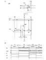
図1は本発明の一態様の入出力装置100の構成を説明する図である。図1(A)は本発
明の一態様の入出力装置の構成を説明する回路図である。図1(B)は図1(A)に示す
入出力装置の駆動方法を説明するタイミングチャートである。FIG. 1 illustrates a structure of an input /
<入出力装置の構成例>
本実施の形態で説明する入出力装置100は、選択信号、制御信号、表示情報を含む表示
信号および検知信号を供給され、検知信号に基づく電位を供給することができる入出力回
路103を有する。<Example of configuration of input / output device>
The input /
また、高電源電位を供給され高電源電位に基づく電位および検知信号に基づいて検知情報
を供給することができる変換回路104を有する。Further, a
また、検知信号を供給することができる検知素子Cと、所定の電流を供給される表示素子
Dと、を有する。Further, it has a sensing element C capable of supplying a sensing signal and a display element D supplied with a predetermined current.
また、入出力回路103は、ゲートが選択信号を供給することができる第1の制御線G1
と電気的に接続され、第1の電極が表示信号を供給することができる信号線DLと電気的
に接続される第1のトランジスタM1を備える。The input /
A first transistor M1 that is electrically connected to the first electrode and electrically connected to a signal line DL whose first electrode can supply a display signal.
ゲートが制御信号を供給することができる第2の制御線G2と電気的に接続され、第1の
電極が第1の配線L1と電気的に接続される第2のトランジスタM2を備える。The semiconductor device includes a second transistor M2 whose gate is electrically connected to a second control line G2 which can supply a control signal, and whose first electrode is electrically connected to a first wiring L1.
また、ゲートが第1のトランジスタM1の第2の電極と電気的に接続され、第1の電極が
第2の配線L2と電気的に接続され、第2の電極が第2のトランジスタM2の第2の電極
と電気的に接続される駆動トランジスタM0を備える。Further, the gate is electrically connected to the second electrode of the first transistor M1, the first electrode is electrically connected to the second wiring L2, and the second electrode is the second electrode of the second transistor M2. A driving transistor M0 electrically connected to the second electrode.
変換回路104は、ゲートが高電源電位を供給することができる配線BRと電気的に接続
され、第1の電極が高電源電位を供給することができる配線VPOと電気的に接続され、
第2の電極が第2の配線L2と電気的に接続されるトランジスタM6と、第2の配線L2
と電気的に接続され且つ検知情報を供給することができる端子OUTと、を備える。The
A transistor M6 having a second electrode electrically connected to the second wiring L2, and a second wiring L2
And a terminal OUT which is electrically connected to the terminal and can supply detection information.
検知素子Cは、第1の電極が第1のトランジスタM1の第2の電極と電気的に接続され、
第2の電極が第2のトランジスタM2の第2の電極と電気的に接続される。The sensing element C has a first electrode electrically connected to a second electrode of the first transistor M1,
The second electrode is electrically connected to the second electrode of the second transistor M2.
表示素子Dは、第1の電極が駆動トランジスタM0の第2の電極と電気的に接続され、第
2の電極が第3の配線L3と電気的に接続される。The display element D has a first electrode electrically connected to the second electrode of the driving transistor M0, and a second electrode electrically connected to the third wiring L3.
本実施の形態で例示する入出力装置100は、選択信号、制御信号、表示情報を含む表示
信号および検知信号を供給され、検知信号に基づく電位を供給する入出力回路103と、
検知信号に基づく検知情報を供給することができる変換回路104と、検知信号を供給す
る検知素子Cと、所定の電流を供給される表示素子Dと、を含んで構成される。The input /
It includes a
これにより、検知素子が供給する検知信号に基づいて変化する電位を用いて検知情報を供
給し、表示信号に基づいて所定の電流を用いて表示素子に表示情報を表示することができ
る。その結果、利便性または信頼性に優れた新規な入出力装置を提供できる。Thus, detection information can be supplied using a potential that changes based on a detection signal supplied by the detection element, and display information can be displayed on the display element using a predetermined current based on the display signal. As a result, a novel input / output device with excellent convenience or reliability can be provided.
なお、駆動トランジスタM0は検知素子Cが供給する検知信号を増幅することができる。Note that the drive transistor M0 can amplify the detection signal supplied by the detection element C.
なお、配線VPOおよび配線BRは、入出力装置100が備えるトランジスタを動作する
ことができる程度に高い電源電位を供給することができる。Note that the wiring VPO and the wiring BR can supply a power supply potential which is high enough to operate a transistor included in the input /
また、第1の配線L1は第1の電源電位を供給することができ、第3の配線L3は第2の
電源電位を供給することができる。なお、第2の電源電位は好ましくは第1の電源電位よ
り高い。Further, the first wiring L1 can supply a first power supply potential, and the third wiring L3 can supply a second power supply potential. Note that the second power supply potential is preferably higher than the first power supply potential.
以下に、入出力装置100を構成する個々の要素について説明する。なお、これらの構成
は明確に分離できず、一つの構成が他の構成を兼ねる場合や他の構成の一部を含む場合が
ある。In the following, individual components of the input /
例えば検知素子および表示素子と電気的に接続された入出力回路は、検知素子の駆動回路
であるとともに表示素子の駆動回路でもある。For example, an input / output circuit electrically connected to the detection element and the display element is a drive circuit for the detection element and a drive circuit for the display element.
《全体の構成》
入出力装置100は、入出力回路103、変換回路104、検知素子Cまたは表示素子D
を有する。《Overall configuration》
The input /
Having.
《入出力回路》
入出力回路103は、第1のトランジスタM1、第2のトランジスタM2または駆動トラ
ンジスタM0を備える。なお、駆動トランジスタは時分割階調方式(デジタル駆動方式と
もいう)を用いて表示素子を駆動してもよいし、電流階調方式(アナログ駆動方式ともい
う)を用いて表示素子を駆動してもよい。《I / O circuit》
The input /
同一の工程で作製することができるトランジスタを、第1のトランジスタM1、第2のト
ランジスタM2および駆動トランジスタM0に用いることができる。これにより、作製工
程が簡略化された入出力回路を提供できる。Transistors that can be manufactured in the same process can be used for the first transistor M1, the second transistor M2, and the driving transistor M0. Thus, an input / output circuit with a simplified manufacturing process can be provided.
なお、選択信号に基づいて導通状態または非導通状態にすることができるスイッチを、第
1のトランジスタM1に換えて用いることができる。Note that a switch that can be turned on or off based on a selection signal can be used instead of the first transistor M1.
また、制御信号に基づいて導通状態または非導通状態にすることができるスイッチを第2
のトランジスタM2に換えて用いることができる。Also, a switch that can be turned on or off based on a control signal is a second switch.
Can be used in place of the transistor M2.
第1のトランジスタM1、第2のトランジスタM2または駆動トランジスタM0は半導体
層を有する。The first transistor M1, the second transistor M2, or the driving transistor M0 has a semiconductor layer.
例えば、4族の元素、化合物半導体または酸化物半導体を半導体層に用いることができる
。具体的には、シリコンを含む半導体、ガリウムヒ素を含む半導体またはインジウムを含
む酸化物半導体などを半導体層に適用できる。また、単結晶、多結晶または非晶質等を含
む半導体、具体的には、単結晶シリコン、ポリシリコンまたはアモルファスシリコンなど
を用いることができる。For example, a Group 4 element, a compound semiconductor, or an oxide semiconductor can be used for the semiconductor layer. Specifically, a semiconductor containing silicon, a semiconductor containing gallium arsenide, an oxide semiconductor containing indium, or the like can be used for the semiconductor layer. In addition, a semiconductor including single crystal, polycrystal, amorphous, or the like, specifically, single crystal silicon, polysilicon, amorphous silicon, or the like can be used.
なお、酸化物半導体を半導体層に適用したトランジスタの構成を、実施の形態5において
詳細に説明する。Note that a structure of a transistor in which an oxide semiconductor is used for a semiconductor layer is described in detail in
入出力回路103は、第1の制御線G1、第2の制御線G2、信号線DL、第1の配線L
1、第2の配線L2または第3の配線L3と電気的に接続される。The input /
First, it is electrically connected to the second wiring L2 or the third wiring L3.
第1の制御線G1は、選択信号を供給することができる。The first control line G1 can supply a selection signal.
第2の制御線G2は、制御信号を供給することができる。The second control line G2 can supply a control signal.
信号線DLは、表示信号を供給することができる。The signal line DL can supply a display signal.
第1の配線L1は、第1の電源電位を供給することができる。The first wiring L1 can supply a first power supply potential.
第2の配線L2は、高電源電位に基づく電位を供給することができる。The second wiring L2 can supply a potential based on a high power supply potential.
第3の配線L3は、第2の電源電位を供給することができる。The third wiring L3 can supply a second power supply potential.
導電性を有する材料を第1の制御線G1、第2の制御線G2、信号線DL、第1の配線L
1、第2の配線L2または第3の配線L3等に用いる。The first conductive line G1, the second control line G2, the signal line DL, the first wiring L
1, used for the second wiring L2, the third wiring L3, or the like.
例えば、無機導電性材料、有機導電性材料、金属または導電性セラミックスなどを配線に
用いることができる。For example, an inorganic conductive material, an organic conductive material, a metal, a conductive ceramic, or the like can be used for the wiring.
具体的には、アルミニウム、金、白金、銀、クロム、タンタル、チタン、モリブデン、タ
ングステン、ニッケル、鉄、コバルト、パラジウムまたはマンガンから選ばれた金属元素
、上述した金属元素を含む合金または上述した金属元素を組み合わせた合金などを配線等
に用いることができる。Specifically, a metal element selected from aluminum, gold, platinum, silver, chromium, tantalum, titanium, molybdenum, tungsten, nickel, iron, cobalt, palladium or manganese, an alloy containing the aforementioned metal element, or an above-described metal An alloy in which elements are combined can be used for the wiring and the like.
または、酸化インジウム、インジウム錫酸化物、インジウム亜鉛酸化物、酸化亜鉛、ガリ
ウムを添加した酸化亜鉛などの導電性酸化物を用いることができる。Alternatively, a conductive oxide such as indium oxide, indium tin oxide, indium zinc oxide, zinc oxide, or zinc oxide to which gallium is added can be used.
または、グラフェンまたはグラファイトを用いることができる。グラフェンを含む膜は、
例えば膜状に形成された酸化グラフェンを含む膜を還元して形成することができる。還元
する方法としては、熱を加える方法や還元剤を用いる方法等を挙げることができる。Alternatively, graphene or graphite can be used. The film containing graphene is
For example, it can be formed by reducing a film containing graphene oxide formed in a film shape. Examples of the method of reduction include a method of applying heat and a method of using a reducing agent.
または、導電性高分子を用いることができる。Alternatively, a conductive polymer can be used.
なお、入出力回路103を支持する基材に入出力回路103を形成するための膜を成膜し
、加工する方法を用いて、入出力回路103を形成してもよい。Note that the input /
または、入出力回路103を支持する基材に他の基材に形成された入出力回路103を転
置する方法を用いて、入出力回路103を形成してもよい。入出力回路103の作製方法
の一例を、実施の形態6乃至実施の形態8において詳細に説明する。Alternatively, the input /
《変換回路》
高電源電位に基づく電位および第1の配線L1を流れる電流の大きさに基づいて検知情報
を端子OUTに供給することができるさまざまな回路を、変換回路104に用いることが
できる。《Conversion circuit》
Various circuits that can supply detection information to the terminal OUT based on the potential based on the high power supply potential and the magnitude of the current flowing through the first wiring L1 can be used for the
例えば、入出力回路103に電気的に接続をすることにより、ソースフォロワ回路または
カレントミラー回路などが構成される回路を、変換回路104に用いることができる。For example, a circuit including a source follower circuit, a current mirror circuit, or the like by being electrically connected to the input /
具体的には、ゲートが配線BRと電気的に接続し、第1の電極が配線VPOと電気的に接
続し、第2の電極が第2の配線L2と電気的に接続するトランジスタM6を備える回路を
、変換回路104に用いることができる。Specifically, a transistor M6 is provided in which a gate is electrically connected to the wiring BR, a first electrode is electrically connected to the wiring VPO, and a second electrode is electrically connected to the second wiring L2. A circuit can be used for the
例えば、トランジスタを駆動できる程度に高い電源電位を配線VPOおよび配線BRに供
給し、変換回路104と入出力回路103とでソースフォロワ回路を構成できる(図1(
A)参照)。For example, a power supply potential that is high enough to drive a transistor is supplied to the wiring VPO and the wiring BR, and a source follower circuit can be formed using the
A)).
入出力回路103に用いることができるトランジスタと同様の構成を備えるトランジスタ
を、トランジスタM6に用いることができる。A transistor having a structure similar to that of the transistor which can be used for the input /
入出力回路103に用いることができる配線と同様の配線を、配線VPOおよび配線BR
に用いることができる。A wiring similar to the wiring that can be used for the input /
Can be used.
なお、入出力回路103を支持する基材を用いて変換回路104を支持してもよい。Note that the
また、入出力回路103を形成する工程と同一の工程を用いて変換回路104を形成して
もよい。Further, the
《検知素子》
検知素子Cは、例えば静電容量、照度、磁力、電波または圧力等を検知して、検知した物
理量に基づく電圧を第1の電極と第2の電極に供給する。《Sensing element》
The detection element C detects, for example, capacitance, illuminance, magnetic force, radio wave, pressure, or the like, and supplies a voltage based on the detected physical quantity to the first electrode and the second electrode.
例えば、容量素子、光電変換素子、磁気検知素子、圧電素子または共振器等を検知素子に
用いることができる。For example, a capacitive element, a photoelectric conversion element, a magnetic sensing element, a piezoelectric element, a resonator, or the like can be used as the sensing element.
具体的には、静電容量の変化に基づいて変化する電圧を含む検知信号を供給する検知素子
を検知素子Cに用いることができる。例えば大気中において、指などの大気より大きな誘
電率を備えるものが導電膜に近接すると、指と導電膜の間の静電容量が変化する。この静
電容量の変化を検知して検知信号を供給することができる。具体的には、導電膜および当
該導電膜に一方の電極が接続された容量素子を検知素子Cに用いることができる。電荷の
分配が静電容量の変化に伴い引き起こされ、容量素子の両端の電極の電圧が変化する。こ
の電圧の変化を検知信号に用いることができる。Specifically, a detection element that supplies a detection signal including a voltage that changes based on a change in capacitance can be used as the detection element C. For example, in the air, when a finger or the like having a higher dielectric constant than the air approaches the conductive film, the capacitance between the finger and the conductive film changes. A detection signal can be supplied by detecting the change in the capacitance. Specifically, a sensing element C can be a conductive film and a capacitor in which one electrode is connected to the conductive film. The distribution of electric charge is caused by the change of the capacitance, and the voltage of the electrodes at both ends of the capacitor changes. This change in voltage can be used as a detection signal.
《表示素子》
表示素子Dは、表示信号に基づく電流を供給され、表示情報を表示する。《Display element》
The display element D is supplied with a current based on a display signal, and displays display information.
例えば、有機エレクトロルミネッセンス素子または発光ダイオード等を、表示素子Dに用
いることができる。For example, an organic electroluminescence element or a light emitting diode can be used for the display element D.
具体的には、第1の電極と、第1の電極に重なる第2の電極と、第1の電極ならびに第2
の電極の間に発光性の有機化合物を含む層を備える発光素子(有機エレクトロルミネッセ
ンス素子または有機EL素子という)を表示素子Dに用いることができる。Specifically, a first electrode, a second electrode overlapping the first electrode, a first electrode and a second electrode
A light-emitting element provided with a layer containing a light-emitting organic compound between the electrodes (referred to as an organic electroluminescence element or an organic EL element) can be used for the display element D.
<入出力装置の駆動方法>
検知素子Cが供給する電圧に基づく検知情報を供給し、供給される表示信号に基づいて表
示を行う入出力装置100の駆動方法を説明する(図1(A)および図1(B)参照)。<Driving method of input / output device>
A driving method of the input /
《第1のステップ》
第1のステップにおいて、第1のトランジスタM1を導通状態にすることができる選択信
号を供給し、第2のトランジスタM2を導通状態にすることができる制御信号を供給し、
基準電位の表示信号を供給する(図1(B)における期間T1を参照)。<< First step >>
In a first step, supplying a selection signal capable of turning on the first transistor M1 and supplying a control signal capable of turning on the second transistor M2;
A display signal of a reference potential is supplied (see a period T1 in FIG. 1B).
これにより、第1のトランジスタM1の第2の電極、駆動トランジスタM0のゲートおよ
び検知素子Cの第1の電極が電気的に接続するノードAの電位を、信号線DLが供給する
基準電位に基づく電位にリセットすることができる。Accordingly, the potential of the node A to which the second electrode of the first transistor M1, the gate of the driving transistor M0, and the first electrode of the sensing element C are electrically connected is based on the reference potential supplied by the signal line DL. It can be reset to the potential.
また、第2のトランジスタM2の第2の電極、駆動トランジスタM0の第2の電極、表示
素子Dの第1の電極および検知素子Cの第2の電極が電気的に接続するノードBの電位を
、第1の配線L1が供給する第1の電源電位に基づく電位にすることができる。In addition, the potential of the node B to which the second electrode of the second transistor M2, the second electrode of the driving transistor M0, the first electrode of the display element D, and the second electrode of the sensing element C are electrically connected is set. , The first power supply potential supplied by the first wiring L1.
《第2のステップ》
第1のトランジスタM1を非導通状態にすることができる選択信号を供給し、第2のトラ
ンジスタM2を導通状態にすることができる制御信号を供給し、駆動トランジスタM0が
所定の電流を供給するように高電源電位に基づく電位を供給し且つ変換回路が検知信号に
基づいて検知情報を供給する(図1(B)における期間T2を参照)。《Second step》
A selection signal capable of turning on the first transistor M1 is supplied, a control signal capable of turning on the second transistor M2 is supplied, and the driving transistor M0 supplies a predetermined current. And a conversion circuit supplies detection information based on the detection signal (see a period T2 in FIG. 1B).
これにより、ノードAの電位を検知素子Cが供給する検知信号に基づく電位にすることが
できる。Thus, the potential of the node A can be set to a potential based on the detection signal supplied from the detection element C.
また、ゲートにノードAの電位を供給される駆動トランジスタM0は、ノードAの電位に
基づいて所定の電流を第2の配線L2から第1の配線L1に供給する。Further, the driving transistor M0 whose gate is supplied with the potential of the node A supplies a predetermined current from the second wiring L2 to the first wiring L1 based on the potential of the node A.
変換回路104は、電流または第2の配線L2に所定の電流を流すのに要する電圧に基づ
いて検知情報を端子OUTに供給する。なお、指などの大気より大きな誘電率を備えるも
のを検知素子Cが検知している状態と、検知していない状態と、において観測される、第
2の配線L2を流れる電流の差を、検知情報としてもよい。または、指などの大気より大
きな誘電率を備えるものを検知素子Cが検知している状態と、検知していない状態と、に
おいて観測される、所定の電流を第2の配線L2に流すために必要な電圧の差を、検知情
報としてもよい。また、検知情報を繰り返し取得して、履歴との差分を利用してもよい。The
《第3のステップ》
第1のトランジスタM1を導通状態にすることができる選択信号を供給し、第2のトラン
ジスタM2を非導通状態にすることができる制御信号を供給し、表示情報に基づく電位の
表示信号を供給する(図1(B)における期間T3を参照)。《Third step》
A selection signal for turning on the first transistor M1 is supplied, a control signal for turning on the second transistor M2 is supplied, and a display signal of a potential based on display information is supplied. (See a period T3 in FIG. 1B).
これにより、ノードAの電位を信号線DLが供給する表示信号に基づく電位にすることが
できる。Thus, the potential of the node A can be set to a potential based on the display signal supplied from the signal line DL.
また、ゲートにノードAの電位を供給される駆動トランジスタM0は、ノードAの電位に
基づいて第2の配線L2から表示素子Dに所定の電流を供給する。Further, the driving transistor M0 whose gate is supplied with the potential of the node A supplies a predetermined current to the display element D from the second wiring L2 based on the potential of the node A.
《第4のステップ》
第1のトランジスタM1を非導通状態にすることができる選択信号を供給し、第2のトラ
ンジスタM2を非導通状態にすることができる制御信号を供給し、第3のステップで供給
された表示信号に基づいて駆動トランジスタM0が所定の電流を供給するように高電源電
位に基づく電位を供給する(図1(B)における期間T4を参照)。<< 4th step >>
A selection signal that can turn off the first transistor M1; a control signal that can turn off the second transistor M2; and a display signal that is supplied in the third step. , The drive transistor M0 supplies a potential based on the high power supply potential so as to supply a predetermined current (see a period T4 in FIG. 1B).
これにより、ノードAの電位は信号線DLが供給する表示信号に基づく電位に保持され、
ノードAの電位をゲートに供給される駆動トランジスタM0は、表示信号に基づく所定の
電流を表示素子Dに供給する。Accordingly, the potential of the node A is held at a potential based on the display signal supplied from the signal line DL,
The driving transistor M0 supplied with the potential of the node A to the gate supplies a predetermined current based on the display signal to the display element D.
なお、表示情報を表示している場合であっても、指などが検知素子Cに近接すると、ノー
ドAの電位が変動してしまう場合がある。しかし、ノードAの電位の変動に伴う表示素子
Dの表示の変化は、指などに遮られ、使用者に視認されにくい。Note that even when display information is displayed, the potential of the node A may fluctuate when a finger or the like approaches the detection element C. However, a change in the display of the display element D due to a change in the potential of the node A is blocked by a finger or the like, and is difficult to be visually recognized by a user.
本実施の形態で説明する入出力装置100の駆動方法は、第1のトランジスタM1を非導
通状態にし、第2のトランジスタM2を導通状態にし、駆動トランジスタM0のゲートと
第2の電極の電圧を、検知素子Cの第1の電極と第2の電極の電圧にするステップを含ん
で構成される。In the method for driving the input /
これにより、検知素子Cが供給する検知信号に基づいて駆動トランジスタM0が供給する
電流または所定の電流を供給するための電圧を、変換回路104を用いて検知情報に変換
し、供給することができる。その結果、利便性または信頼性に優れた新規な入出力装置の
駆動方法を提供できる。Accordingly, the current supplied by the drive transistor M0 or the voltage for supplying the predetermined current based on the detection signal supplied by the detection element C can be converted into detection information by using the
なお、本実施の形態は、本明細書で示す他の実施の形態と適宜組み合わせることができる
。Note that this embodiment can be combined with any of the other embodiments in this specification as appropriate.
(実施の形態2)
本実施の形態では、本発明の一態様の入出力装置の構成について、図2を参照しながら説
明する。(Embodiment 2)
In this embodiment, a structure of the input / output device of one embodiment of the present invention will be described with reference to FIGS.
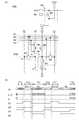
図2は本発明の一態様の入出力装置100Bの構成を説明する図である。図2(A)は本
発明の一態様の入出力装置の構成を説明する回路図である。図2(B)は図2(A)に示
す入出力装置の駆動方法を説明するタイミングチャートである。FIG. 2 illustrates a configuration of the input /
<入出力装置の構成例>
本実施の形態で説明する入出力装置100Bは、選択信号、第1の制御信号乃至第3の制
御信号、表示情報を含む表示信号および検知信号を供給され、検知信号に基づく電位を供
給することができる入出力回路103Bを有する。<Example of configuration of input / output device>
The input /
高電源電位を供給され高電源電位に基づく電位および検知信号に基づいて検知情報を供給
することができる変換回路104を有する。A
検知信号を供給することができる検知素子Cと、所定の電流を供給される表示素子Dを有
する。It has a detection element C that can supply a detection signal and a display element D that is supplied with a predetermined current.
入出力回路103Bは、ゲートが選択信号を供給することができる第1の制御線G1と電
気的に接続され、第1の電極が表示信号を供給することができる信号線DLと電気的に接
続される第1のトランジスタM1を備える。The input /
また、ゲートが第1の制御信号を供給することができる第2の制御線G2と電気的に接続
され、第1の電極が第1の配線L1と電気的に接続される第2のトランジスタM2を備え
る。In addition, a second transistor M2 whose gate is electrically connected to a second control line G2 which can supply a first control signal, and whose first electrode is electrically connected to a first wiring L1. Is provided.
また、ゲートが第2の制御信号を供給することができる第3の制御線G3と電気的に接続
され、第1の電極が第2のトランジスタM2の第2の電極と電気的に接続される第3のト
ランジスタM3を備える。In addition, a gate is electrically connected to a third control line G3 which can supply a second control signal, and a first electrode is electrically connected to a second electrode of the second transistor M2. The third transistor M3 is provided.
また、ゲートが第3の制御信号を供給することができる第4の制御線G4と電気的に接続
され、第1の電極が第1のトランジスタM1の第2の電極と電気的に接続される第4のト
ランジスタM4を備える。In addition, a gate is electrically connected to a fourth control line G4 which can supply a third control signal, and a first electrode is electrically connected to a second electrode of the first transistor M1. A fourth transistor M4 is provided.
また、ゲートが選択信号を供給することができる第1の制御線G1と電気的に接続され、
第1の電極が第4のトランジスタM4の第2の電極と電気的に接続され、第2の電極が第
4の配線L4と電気的に接続される第5のトランジスタM5を備える。A gate is electrically connected to a first control line G1 that can supply a selection signal;
The semiconductor device includes a fifth transistor M5 whose first electrode is electrically connected to the second electrode of the fourth transistor M4 and whose second electrode is electrically connected to the fourth wiring L4.
また、ゲートが第4のトランジスタM4の第2の電極と電気的に接続され、第1の電極が
第2の配線L2と電気的に接続され、第2の電極が第2のトランジスタM2の第2の電極
と電気的に接続される駆動トランジスタM0を備える。Further, the gate is electrically connected to the second electrode of the fourth transistor M4, the first electrode is electrically connected to the second wiring L2, and the second electrode is connected to the second electrode of the second transistor M2. A driving transistor M0 electrically connected to the second electrode.
変換回路104は、ゲートが高電源電位を供給することができる配線BRと電気的に接続
され、第1の電極が高電源電位を供給することができる配線VPOと電気的に接続され、
第2の電極が第2の配線L2と電気的に接続されるトランジスタM6と、第2の配線L2
と電気的に接続され且つ検知情報を供給することができる端子OUTを備える。The
A transistor M6 having a second electrode electrically connected to the second wiring L2, and a second wiring L2
And a terminal OUT that is electrically connected to and can supply detection information.
検知素子Cは、第1の電極が第1のトランジスタM1の第2の電極と電気的に接続され、
第2の電極が第2のトランジスタM2の第2の電極と電気的に接続される。The sensing element C has a first electrode electrically connected to a second electrode of the first transistor M1,
The second electrode is electrically connected to the second electrode of the second transistor M2.
表示素子Dは、第1の電極が第3のトランジスタM3の第2の電極と電気的に接続され、
第2の電極が第3の配線L3と電気的に接続される。The display element D has a first electrode electrically connected to a second electrode of the third transistor M3,
The second electrode is electrically connected to third wiring L3.
本実施の形態で例示する入出力装置100Bは、選択信号、制御信号、表示情報を含む表
示信号および検知信号を供給され、検知信号に基づく電位を供給する入出力回路103B
と、検知信号に基づく検知情報を供給することができる変換回路104と、検知信号を供
給する検知素子Cと、所定の電流を供給される表示素子Dと、を含んで構成される。The input /
And a
これにより、検知素子が供給する検知信号に基づいて変化する電位を用いて検知情報を供
給し、表示信号に基づいて変化する所定の電流を用いて表示素子に表示情報を表示するこ
とができる。その結果、利便性または信頼性に優れた新規な入出力装置を提供できる。Thus, the detection information can be supplied using the potential that changes based on the detection signal supplied by the detection element, and the display information can be displayed on the display element using the predetermined current that changes based on the display signal. As a result, a novel input / output device with excellent convenience or reliability can be provided.
なお、配線VPOおよび配線BRは、入出力装置100Bが備えるトランジスタを動作す
ることができる程度に高い電源電位を供給することができる。Note that the wiring VPO and the wiring BR can supply a power supply potential which is high enough to operate a transistor included in the input /
また、第1の配線L1は第1の電源電位を供給することができ、第3の配線L3は第2の
電源電位を供給することができ、第4の配線L4は第3の電源電位を供給することができ
る。なお、第2の電源電位は好ましくは第1の電源電位より高い。また、第3の電源電位
は第1の電源電位および第2の電源電位より高く且つ第1の制御信号のハイの電位より低
い電位が好ましい。具体的には、第1の電源電位を−5Vとし、第2の電源電位を−3V
とし、第3の電源電位を+6Vとし、第1の制御信号のハイの電位を+15Vとすること
ができる。The first wiring L1 can supply a first power supply potential, the third wiring L3 can supply a second power supply potential, and the fourth wiring L4 can supply a third power supply potential. Can be supplied. Note that the second power supply potential is preferably higher than the first power supply potential. The third power supply potential is preferably higher than the first power supply potential and the second power supply potential and lower than the high potential of the first control signal. Specifically, the first power supply potential is set to -5 V, and the second power supply potential is set to -3 V
The third power supply potential can be set to +6 V, and the high potential of the first control signal can be set to +15 V.
以下に、入出力装置100Bを構成する個々の要素について説明する。なお、これらの構
成は明確に分離できず、一つの構成が他の構成を兼ねる場合や他の構成の一部を含む場合
がある。Hereinafter, the individual elements constituting the input /
例えば検知素子および表示素子と電気的に接続された入出力回路は、検知素子の駆動回路
であるとともに表示素子の駆動回路でもある。For example, an input / output circuit electrically connected to the detection element and the display element is a drive circuit for the detection element and a drive circuit for the display element.
入出力装置100Bは、入出力回路103Bが第3のトランジスタM3乃至第5のトラン
ジスタM5を有する点、第3の制御線G3および第4の制御線G4と電気的に接続される
点が、図1を参照しながら説明する入出力装置100とは異なる。ここでは異なる構成に
ついて詳細に説明し、同様の構成を用いることができる部分は、上記の説明を援用する。The input /
《全体の構成》
入出力装置100Bは、入出力回路103B、変換回路104、検知素子Cまたは表示素
子Dを有する。《Overall configuration》
The input /
《入出力回路》
入出力回路103Bは、第1のトランジスタM1乃至第5のトランジスタM5または駆動
トランジスタM0を備える。《I / O circuit》
The input /
同一の工程で作製することができるトランジスタを、第1のトランジスタM1乃至第5の
トランジスタM5および駆動トランジスタM0に用いることができる。これにより、作製
工程が簡略化された入出力回路を提供できる。Transistors that can be manufactured in the same process can be used for the first to fifth transistors M1 to M5 and the driving transistor M0. Thus, an input / output circuit with a simplified manufacturing process can be provided.
なお、選択信号に基づいて導通状態または非導通状態にすることができるスイッチを、第
1のトランジスタM1または第5のトランジスタM5に換えて用いることができる。Note that a switch that can be turned on or off based on a selection signal can be used instead of the first transistor M1 or the fifth transistor M5.
また、第1の制御信号に基づいて導通状態または非導通状態にすることができるスイッチ
を第2のトランジスタM2に換えて用いることができる。Further, a switch that can be turned on or off based on the first control signal can be used instead of the second transistor M2.
また、第2の制御信号に基づいて導通状態または非導通状態にすることができるスイッチ
を第3のトランジスタM3に換えて用いることができる。Further, a switch that can be turned on or off based on the second control signal can be used instead of the third transistor M3.
また、第3の制御信号に基づいて導通状態または非導通状態にすることができるスイッチ
を第4のトランジスタM4に換えて用いることができる。Further, a switch that can be turned on or off based on the third control signal can be used instead of the fourth transistor M4.
第1のトランジスタM1乃至第5のトランジスタM5または駆動トランジスタM0は半導
体層を有する。Each of the first to fifth transistors M1 to M5 or the driving transistor M0 has a semiconductor layer.
例えば、実施の形態1で説明する入出力装置100に用いることができるトランジスタと
同様の構成を、入出力装置100Bのトランジスタに用いることができる。For example, a structure similar to that of the transistor which can be used for the input /
入出力回路103Bは、第1の制御線G1乃至第4の制御線G4、信号線DL、第1の配
線L1乃至第4の配線L4と電気的に接続される。The input /
第1の制御線G1は、選択信号を供給することができる。The first control line G1 can supply a selection signal.
第2の制御線G2は第1の制御信号を供給することができ、第3の制御線G3は第2の制
御信号を供給することができ、第4の制御線G4は第3の制御信号を供給することができ
る。The second control line G2 can supply a first control signal, the third control line G3 can supply a second control signal, and the fourth control line G4 can supply a third control signal. Can be supplied.
信号線DLは、表示信号を供給することができる。The signal line DL can supply a display signal.
第1の配線L1は、第1の電源電位を供給することができる。The first wiring L1 can supply a first power supply potential.
第2の配線L2は、高電源電位に基づく電位を供給することができる。The second wiring L2 can supply a potential based on a high power supply potential.
第3の配線L3は、第2の電源電位を供給することができる。The third wiring L3 can supply a second power supply potential.
第4の配線L4は、第3の電源電位を供給することができる。The fourth wiring L4 can supply a third power supply potential.
例えば、実施の形態1で説明する入出力装置100に用いることができる配線と同様の構
成を、入出力装置100Bの配線に用いる。For example, a structure similar to the wiring that can be used for the input /
<入出力装置の駆動方法>
検知素子Cが供給する電圧に基づく検知情報を供給し、供給される表示信号に基づいて表
示を行う入出力装置100Bの駆動方法を説明する(図2(A)および図2(B)参照)
。<Driving method of input / output device>
A driving method of the input /
.
《第1のステップ》
第1のステップにおいて、第1のトランジスタM1および第5のトランジスタM5を非導
通状態にすることができる選択信号、第2のトランジスタM2を非導通状態にすることが
できる第1の制御信号、第3のトランジスタM3を導通状態にすることができる第2の制
御信号および第4のトランジスタM4を非導通状態にすることができる第3の制御信号を
供給する(図2(B)における期間T11を参照)。<< First step >>
In the first step, a selection signal capable of turning off the first transistor M1 and the fifth transistor M5, a first control signal capable of turning off the second transistor M2, A second control signal capable of turning on the third transistor M3 and a third control signal capable of turning off the fourth transistor M4 are supplied (period T11 in FIG. 2B). reference).
これにより、第2のトランジスタM2の第2の電極、第3のトランジスタM3の第1の電
極、駆動トランジスタM0の第2の電極および検知素子Cの第2の電極が電気的に接続す
るノードBの電位を第2の電源電位より表示素子Dが動作するか否かの電圧(閾値の電圧
ともいえる)だけ高い電位にすることができる。その結果、第2のステップ以降において
変化するノードBの電位を、表示素子Dの閾値の電圧に基づく電位にすることができる。
また、例えば駆動トランジスタM0の閾値電圧Vthがプラス側にシフトしている場合で
も、選択信号に基づいて駆動トランジスタM0を導通状態にすることができる。Thereby, the node B to which the second electrode of the second transistor M2, the first electrode of the third transistor M3, the second electrode of the driving transistor M0, and the second electrode of the sensing element C are electrically connected. Can be made higher than the second power supply potential by a voltage (which can also be referred to as a threshold voltage) that determines whether or not the display element D operates. As a result, the potential of the node B that changes after the second step can be set to a potential based on the threshold voltage of the display element D.
Further, for example, even when the threshold voltage Vth of the driving transistor M0 is shifted to the plus side, the driving transistor M0 can be turned on based on the selection signal.
《第2のステップ》
第2のステップにおいて、第1のトランジスタM1および第5のトランジスタM5を導通
状態にすることができる選択信号、第2のトランジスタM2を非導通状態にすることがで
きる第1の制御信号、第3のトランジスタM3を非導通状態にすることができる第2の制
御信号、第4のトランジスタM4を非導通状態にすることができる第3の制御信号および
基準電位の表示信号を供給する(図2(B)における期間T12を参照)。《Second step》
In a second step, a selection signal capable of turning on the first transistor M1 and the fifth transistor M5, a first control signal capable of turning off the second transistor M2, and a third signal. A second control signal capable of turning off the transistor M3, a third control signal capable of turning off the fourth transistor M4, and a display signal of the reference potential (FIG. (See period T12 in B)).
これにより、第1のトランジスタM1の第2の電極、第4のトランジスタM4の第1の電
極および検知素子Cの第1の電極が電気的に接続するノードAの電位を、信号線DLが供
給する基準電位に基づく電位にリセットすることができる。Accordingly, the signal line DL supplies the potential of the node A to which the second electrode of the first transistor M1, the first electrode of the fourth transistor M4, and the first electrode of the sensing element C are electrically connected. Reset to a potential based on the reference potential.
また、駆動トランジスタM0のゲートの電位を第4の配線L4が供給する第3の電源電位
に基づく電位にリセットすることができる。Further, the potential of the gate of the driving transistor M0 can be reset to a potential based on the third power supply potential supplied from the fourth wiring L4.
《第3のステップ》
第3のステップにおいて、第1のトランジスタM1および第5のトランジスタM5を非導
通状態にすることができる選択信号、第2のトランジスタM2を導通状態にすることがで
きる第1の制御信号、第3のトランジスタM3を非導通状態にすることができる第2の制
御信号および第4のトランジスタM4を導通状態にすることができる第3の制御信号なら
びに検知素子Cが供給する検知信号に基づいて駆動トランジスタM0が所定の電流を供給
するように高電源電位に基づく電位を第2の配線L2に供給し且つ変換回路104が検知
信号に基づいて検知情報を供給する(図2(B)における期間T21を参照)。《Third step》
In the third step, a selection signal capable of turning off the first transistor M1 and the fifth transistor M5, a first control signal capable of turning on the second transistor M2, and a third control signal. A second control signal that can make the transistor M3 non-conductive, a third control signal that can make the fourth transistor M4 conductive, and a detection signal supplied by the sensing element C A potential based on the high power supply potential is supplied to the second wiring L2 so that M0 supplies a predetermined current, and the
これにより、ノードBの電位を、第1の配線L1が供給する第1の電源電位に基づく電位
にすることができる。Thus, the potential of the node B can be set to a potential based on the first power supply potential supplied from the first wiring L1.
また、ノードAの電位を検知素子Cが供給する検知信号に基づく電位にすることができる
。Further, the potential of the node A can be set to a potential based on a detection signal supplied from the detection element C.
また、ゲートにノードAの電位を供給される駆動トランジスタM0は、ノードAの電位に
基づいて所定の電流を第2の配線L2から第1の配線L1に供給する。Further, the driving transistor M0 whose gate is supplied with the potential of the node A supplies a predetermined current from the second wiring L2 to the first wiring L1 based on the potential of the node A.
変換回路104は、第2の配線L2を流れる所定の電流に基づいて検知情報を端子OUT
に供給する。The
To supply.
《第4のステップ》
第4のステップにおいて、第1のトランジスタM1および第5のトランジスタM5を非導
通状態にすることができる選択信号、第2のトランジスタM2を非導通状態にすることが
できる第1の制御信号、第3のトランジスタM3を導通状態にすることができる第2の制
御信号および第4のトランジスタM4を非導通状態にすることができる第3の制御信号を
供給する(図2(B)における期間T22を参照)。<< 4th step >>
In a fourth step, a selection signal capable of turning off the first transistor M1 and the fifth transistor M5, a first control signal capable of turning off the second transistor M2, A second control signal capable of turning on the third transistor M3 and a third control signal capable of turning off the fourth transistor M4 are supplied (period T22 in FIG. 2B). reference).
これにより、ノードBの電位を第2の電源電位より表示素子Dが動作するか否かの電位(
閾値の電位ともいえる)だけ高い電位にすることができる。その結果、第5のステップ以
降において変化するノードBの電位を、表示素子Dの閾値の電圧に基づく電位にすること
ができる。また、例えば駆動トランジスタM0の閾値電圧Vthがプラス側にシフトして
いる場合でも、選択信号に基づいて駆動トランジスタM0を導通状態にすることができる
。Thus, the potential of the node B is set to be higher than the potential of the second power supply potential (ie, whether or not the display element D operates).
(A threshold potential). As a result, the potential of the node B that changes after the fifth step can be set to a potential based on the threshold voltage of the display element D. Further, for example, even when the threshold voltage Vth of the driving transistor M0 is shifted to the plus side, the driving transistor M0 can be turned on based on the selection signal.
《第5のステップ》
第5のステップにおいて、第1のトランジスタM1および第5のトランジスタM5を導通
状態にすることができる選択信号、第2のトランジスタM2を非導通状態にすることがで
きる第1の制御信号、第3のトランジスタM3を非導通状態にすることができる第2の制
御信号、第4のトランジスタM4を非導通状態にすることができる第3の制御信号および
表示情報に基づく表示信号を供給する(図2(B)における期間T31を参照)。<< Fifth Step >>
In the fifth step, a selection signal capable of turning on the first transistor M1 and the fifth transistor M5, a first control signal capable of turning off the second transistor M2, and a third signal. A second control signal that can make the transistor M3 non-conductive, a third control signal that can make the fourth transistor M4 non-conductive, and a display signal based on display information are supplied (FIG. 2). (See period T31 in (B)).
これにより、ノードAの電位を信号線DLが供給する表示信号に基づく電位にすることが
できる。Thus, the potential of the node A can be set to a potential based on the display signal supplied from the signal line DL.
また、駆動トランジスタM0のゲートの電位を第4の配線L4が供給する第3の電源電位
に基づく電位にリセットすることができる。Further, the potential of the gate of the driving transistor M0 can be reset to a potential based on the third power supply potential supplied from the fourth wiring L4.
《第6のステップ》
第6のステップにおいて、第1のトランジスタM1および第5のトランジスタM5を非導
通状態にすることができる選択信号、第2のトランジスタM2を非導通状態にすることが
できる第1の制御信号、第3のトランジスタM3を導通状態にすることができる第2の制
御信号、第4のトランジスタM4を導通状態にすることができる第3の制御信号ならびに
第5のステップで供給された表示信号に基づいて駆動トランジスタM0が所定の電流を供
給するように高電源電位を第2の配線L2に供給する(図2(B)における期間T41を
参照)。《Sixth Step》
In the sixth step, a selection signal capable of turning off the first transistor M1 and the fifth transistor M5, a first control signal capable of turning off the second transistor M2, Based on a second control signal capable of turning on the third transistor M3, a third control signal capable of turning on the fourth transistor M4, and the display signal supplied in the fifth step. A high power supply potential is supplied to the second wiring L2 so that the driving transistor M0 supplies a predetermined current (see a period T41 in FIG. 2B).
これにより、ゲートに第5のステップで供給された表示信号に基づく電位が供給された駆
動トランジスタM0は、所定の電流を第3のトランジスタM3を介して表示素子Dに供給
し、表示素子Dは表示信号に基づく表示をする。Thereby, the driving transistor M0 having the gate supplied with the potential based on the display signal supplied in the fifth step supplies a predetermined current to the display element D via the third transistor M3, and the display element D Display based on the display signal.
本実施の形態で説明する入出力装置100Bの駆動方法は、第1のトランジスタM1を非
導通状態にし、第2のトランジスタM2を導通状態にし、駆動トランジスタM0のゲート
と第2の電極の電圧を、検知素子Cの第1の電極と第2の電極の電圧にするステップを含
んで構成される。In the method for driving the input /
これにより、検知素子Cが供給する検知信号に基づいて駆動トランジスタM0が供給する
電流または所定の電流を供給するための電圧を、変換回路104を用いて検知情報に変換
し、供給することができる。その結果、利便性または信頼性に優れた新規な入出力装置の
駆動方法を提供できる。Accordingly, the current supplied by the drive transistor M0 or the voltage for supplying the predetermined current based on the detection signal supplied by the detection element C can be converted into detection information by using the
なお、本実施の形態は、本明細書で示す他の実施の形態と適宜組み合わせることができる
。Note that this embodiment can be combined with any of the other embodiments in this specification as appropriate.
(実施の形態3)
本実施の形態では、本発明の一態様の入出力装置の構成について、図3を参照しながら説
明する。(Embodiment 3)
In this embodiment, a structure of the input / output device of one embodiment of the present invention will be described with reference to FIGS.
図3は本発明の一態様の入出力装置200の構成を説明する図である。図3(A)は本発
明の一態様の入出力装置200の構成を説明するブロック図であり、図3(B)は図3(
A)に示す画素202(i,j)が備える入出力回路203(i,j)の回路図および変
換器CONVが備える変換回路204(j)の回路図である。FIG. 3 illustrates a structure of an input /
3A is a circuit diagram of an input / output circuit 203 (i, j) included in a pixel 202 (i, j) and a circuit diagram of a conversion circuit 204 (j) included in a converter CONV.
<入出力装置の構成例1>
本実施の形態で説明する入出力装置200は、領域201を有する。領域201はm行n
列のマトリクス状に配設される複数の画素202(i,j)を有する。なお、mおよびn
は1以上の自然数であり、mまたはnは2以上である。また、iはm以下であり、jはn
以下である。<Structure example 1 of input / output device>
The input /
It has a plurality of pixels 202 (i, j) arranged in a matrix of columns. Note that m and n
Is a natural number of 1 or more, and m or n is 2 or more. I is equal to or less than m, and j is n
It is as follows.
また、行方向に配設される複数の画素202(i,j)と電気的に接続され且つ選択信号
を供給することができる複数の第1の制御線G1(i)と、行方向に配設される複数の画
素202(i,j)と電気的に接続され且つ制御信号を供給することができる複数の第2
の制御線G2(i)と、を有する。Further, a plurality of first control lines G1 (i) electrically connected to the plurality of pixels 202 (i, j) arranged in the row direction and capable of supplying a selection signal are arranged in the row direction. A plurality of
And a control line G2 (i).
また、列方向に配設される複数の画素202(i,j)と電気的に接続され且つ表示情報
を含む表示信号を供給することができる複数の信号線DL(j)と、列方向に配設される
複数の画素202(i,j)と電気的に接続され且つ第1の電源電位を供給することがで
きる複数の第1の配線L1(j)と、列方向に配設される複数の画素202(i,j)と
電気的に接続され且つ高電源電位に基づく電位を供給することができる複数の第2の配線
L2(j)と、列方向に配設される複数の画素202(i,j)と電気的に接続され且つ
第2の電源電位を供給することができる複数の第3の配線L3(j)と、を有する。A plurality of signal lines DL (j) electrically connected to the plurality of pixels 202 (i, j) arranged in the column direction and capable of supplying a display signal including display information; A plurality of first wirings L1 (j), which are electrically connected to the plurality of pixels 202 (i, j) and can supply a first power supply potential, are provided in the column direction. A plurality of second lines L2 (j) electrically connected to the plurality of pixels 202 (i, j) and capable of supplying a potential based on a high power supply potential; and a plurality of pixels arranged in a column direction 202 (i, j) and a plurality of third wirings L3 (j) that can supply a second power supply potential.
また、第2の配線L2(j)と電気的に接続され且つ高電源電位を供給され高電源電位に
基づく電位および検知信号に基づいて検知情報を供給することができる変換回路204(
j)と、を有する。The conversion circuit 204 (which is electrically connected to the second wiring L2 (j), is supplied with a high power supply potential, and can supply detection information based on a potential based on the high power supply potential and a detection signal.
j).
また、画素202(i,j)、第1の制御線G1(i)、第2の制御線G2(i)、信号
線DL(i)および第1の配線L1(j)乃至第3の配線L3(j)を支持する基材21
0と、を有する。Further, the pixel 202 (i, j), the first control line G1 (i), the second control line G2 (i), the signal line DL (i), the first wiring L1 (j) to the
0.
画素202(i,j)は、選択信号、制御信号および表示信号ならびに検知信号を供給さ
れ、検知信号に基づく電位を供給することができる入出力回路203(i,j)を備える
。The pixel 202 (i, j) is provided with an input / output circuit 203 (i, j) to which a selection signal, a control signal, a display signal, and a detection signal are supplied and which can supply a potential based on the detection signal.
また、検知信号を供給することができる検知素子Cと、所定の電流を供給される表示素子
Dと、を備える。Further, it includes a detection element C that can supply a detection signal and a display element D that is supplied with a predetermined current.
入出力回路203(i,j)は、ゲートが選択信号を供給することができる第1の制御線
G1(i)と電気的に接続され、第1の電極が表示信号を供給することができる信号線D
L(j)と電気的に接続される第1のトランジスタM1を備える。The input / output circuit 203 (i, j) is electrically connected to the first control line G1 (i) whose gate can supply a selection signal, and the first electrode can supply a display signal. Signal line D
A first transistor M1 electrically connected to L (j);
また、ゲートが制御信号を供給することができる第2の制御線G2(i)と電気的に接続
され、第1の電極が第1の配線L1(j)と電気的に接続される第2のトランジスタM2
を備える。In addition, a gate is electrically connected to a second control line G2 (i) that can supply a control signal, and a first electrode is electrically connected to a first wiring L1 (j). Transistor M2
Is provided.
また、ゲートが第1のトランジスタM1の第2の電極と電気的に接続され、第1の電極が
第2の配線L2(j)と電気的に接続され、第2の電極が第2のトランジスタM2の第2
の電極と電気的に接続される駆動トランジスタM0と、を備える。The gate is electrically connected to the second electrode of the first transistor M1, the first electrode is electrically connected to the second wiring L2 (j), and the second electrode is connected to the second transistor. The second of M2
And a driving transistor M0 that is electrically connected to the electrodes.
変換回路204(j)は、ゲートが高電源電位を供給することができる配線BRと電気的
に接続され、第1の電極が高電源電位を供給することができる配線VPOと電気的に接続
され、第2の電極が第2の配線L2(j)と電気的に接続されるトランジスタM6と、第
2の配線L2(j)と電気的に接続され且つ検知情報を供給することができる端子OUT
(j)と、を備える。The conversion circuit 204 (j) is electrically connected to a wiring BR whose gate can supply a high power supply potential, and electrically connected to a wiring VPO whose first electrode can supply a high power supply potential. , A transistor M6 whose second electrode is electrically connected to the second wiring L2 (j), and a terminal OUT which is electrically connected to the second wiring L2 (j) and can supply detection information.
(J).
検知素子Cは、第1の電極が第1のトランジスタM1の第2の電極と電気的に接続され、
第2の電極が第2のトランジスタM2の第2の電極と電気的に接続される。The sensing element C has a first electrode electrically connected to a second electrode of the first transistor M1,
The second electrode is electrically connected to the second electrode of the second transistor M2.
表示素子Dは、第1の電極が駆動トランジスタM0の第2の電極と電気的に接続され、第
2の電極が第3の配線L3(j)と電気的に接続される。The display element D has a first electrode electrically connected to a second electrode of the driving transistor M0, and a second electrode electrically connected to a third wiring L3 (j).
本実施の形態で説明する入出力装置200は、選択信号、制御信号、表示情報を含む表示
信号および検知信号を供給され、検知信号に基づく電位を供給する入出力回路203(i
,j)、検知信号を供給する検知素子Cおよび所定の電流を供給される表示素子Dを備え
る複数の画素202(i,j)と、当該複数の画素202(i,j)がマトリクス状に配
設される基材210と、列方向に配設される画素202(i,j)と電気的に接続され且
つ検知信号に基づく検知情報を供給することができる変換回路204(j)と、を含んで
構成される。The input /
, J), a plurality of pixels 202 (i, j) including a detection element C for supplying a detection signal and a display element D for supplying a predetermined current, and the plurality of pixels 202 (i, j) are arranged in a matrix. A conversion circuit 204 (j) that is electrically connected to the
これにより、マトリクス状に配置された画素が備える検知素子が供給する検知信号に基づ
いて変化する電位を用いて、画素が配置された位置情報と関連付けることができる検知情
報を供給することができる。また、表示信号に基づいて所定の電流を用いてマトリクス状
に配置された画素が備える表示素子に表示情報を表示することができる。その結果、利便
性または信頼性に優れた新規な入出力装置を提供できる。This makes it possible to supply detection information that can be associated with position information where pixels are arranged, using a potential that changes based on a detection signal supplied by a sensing element provided in pixels arranged in a matrix. Further, display information can be displayed on a display element provided in pixels arranged in a matrix using a predetermined current based on a display signal. As a result, a novel input / output device with excellent convenience or reliability can be provided.
本実施の形態で説明する入出力装置200は、検知素子Cと表示素子Dが画素202(i
,j)に配置されている。これにより、検知素子Cを用いて画像が表示される座標を供給
できる。In the input /
, J). Thereby, the coordinates at which the image is displayed using the sensing element C can be supplied.
なお、ノイズの影響を受け難くするために、変換回路204(j)を領域201の外側な
ど、入出力回路から離して配置することができる。Note that the conversion circuit 204 (j) can be arranged away from the input / output circuit, such as outside the
また、検知素子を画素毎に配設せず、複数の画素に一つ検知素子を配設してもよい。これ
により、制御線の数を低減できる。Alternatively, one sensing element may be provided for a plurality of pixels without providing the sensing element for each pixel. Thereby, the number of control lines can be reduced.
また、複数の画像が供給する検知情報を一つの座標情報にまとめてもよい。Further, detection information supplied by a plurality of images may be combined into one piece of coordinate information.
また、基材210が可撓性を有してもよい。可撓性を有する基材210を用いることによ
り、入出力装置200を折り曲げることまたは折り畳むことができるようにしてもよい。Further, the
なお、折り畳むことができる入出力装置200が折り畳まれた状態において、検知素子C
の一部が他の部分に近接して配置される場合がある。これにより、検知素子Cの一部が他
の部分と干渉し、誤検知を生じる場合がある。具体的には、容量素子を検知素子Cに用い
る場合、近接する電極が互いに干渉する。When the foldable input /
May be arranged close to other parts. As a result, a part of the sensing element C may interfere with another part, and erroneous detection may occur. Specifically, when a capacitive element is used for the sensing element C, adjacent electrodes interfere with each other.
折り畳まれる大きさに比べて十分小さな検知素子を入出力装置200に用いることができ
る。これにより、折り畳まれた状態において、検知素子Cの干渉を防ぐことができる。A sensing element that is sufficiently smaller than the size to be folded can be used for the input /
また、マトリクス状に配置された複数の検知素子Cを分離して動作させることができる。
これにより、誤検知を生じる領域に配置された検知素子の動作を停止することができる。Further, the plurality of sensing elements C arranged in a matrix can be operated separately.
Thereby, the operation of the sensing element arranged in the region where the erroneous detection occurs can be stopped.
なお、マトリクス状に配置された画素の一部に検知素子Cおよび表示素子Dを配設しても
よい。例えば、検知素子Cおよび表示素子Dが配設される画素の数を表示素子Dのみが配
設される画素の数より少なくしてもよい。これにより、供給する検知情報より高い精細度
で表示情報を表示することができる。Note that the sensing element C and the display element D may be provided in a part of the pixels arranged in a matrix. For example, the number of pixels provided with the sensing element C and the display element D may be smaller than the number of pixels provided with only the display element D. This makes it possible to display the display information with a higher definition than the supplied detection information.
また、入出力装置200は、選択信号または制御信号を供給する駆動回路GDを有しても
よい。Further, the input /
また、表示信号を供給する駆動回路SDを有してもよい。Further, a driving circuit SD for supplying a display signal may be provided.
また、複数の変換回路204(j)を備え且つ検知情報を供給する変換器CONVを有し
ていてもよい。Further, a converter CONV that includes a plurality of conversion circuits 204 (j) and supplies detection information may be provided.
また、複数の画素202(i,j)を支持する基材210は、駆動回路GD、駆動回路S
Dまたは変換器CONVを支持してもよい。The base 210 supporting the plurality of pixels 202 (i, j) includes the driving circuit GD and the driving circuit S
D or the converter CONV may be supported.
以下に、入出力装置200を構成する個々の要素について説明する。なお、これらの構成
は明確に分離できず、一つの構成が他の構成を兼ねる場合や他の構成の一部を含む場合が
ある。In the following, individual components of the input /
例えば検知素子および表示素子と電気的に接続された入出力回路は、検知素子の駆動回路
であるとともに表示素子の駆動回路でもある。また、検知素子および表示素子を備える画
素は、表示画素であるとともに検知画素でもある。For example, an input / output circuit electrically connected to the detection element and the display element is a drive circuit for the detection element and a drive circuit for the display element. Further, the pixel including the detection element and the display element is a display pixel as well as a detection pixel.
また、入出力装置200は、複数の画素202(i,j)、複数の第1の制御線G1(i
)、複数の第2の制御線G2(i)、複数の信号線DL(j)、複数の第1の配線L1(
j)、複数の第2の配線L2(j)、複数の第3の配線L3(j)および複数の変換回路
204(j)を有する点およびこれらを支持する基材210を有する点が、図1を参照し
ながら説明する入出力装置100とは異なる。ここでは異なる構成について詳細に説明し
、同様の構成を用いることができる部分は、上記の説明を援用する。The input /
), A plurality of second control lines G2 (i), a plurality of signal lines DL (j), a plurality of first lines L1 (
j), a plurality of second wirings L2 (j), a plurality of third wirings L3 (j), a point having a plurality of conversion circuits 204 (j), and a point having a base 210 supporting these. 1 is different from the input /
《全体の構成》
入出力装置200は、画素202(i,j)、第1の制御線G1(i)、第2の制御線G
2(i)、信号線DL(j)、第1の配線L1(j)、第2の配線L2(j)、第3の配
線L3(j)、変換回路204(j)または基材210を有する。《Overall configuration》
The input /
2 (i), the signal line DL (j), the first wiring L1 (j), the second wiring L2 (j), the third wiring L3 (j), the conversion circuit 204 (j) or the
また、選択信号または制御信号を供給する駆動回路GD、表示信号を供給する駆動回路S
Dまたは検知情報を供給する変換器CONVを有していてもよい。Further, a driving circuit GD for supplying a selection signal or a control signal and a driving circuit S for supplying a display signal
D or a converter CONV that supplies the sensing information.
《画素》
領域201はm行n列のマトリクス状に配設される複数の画素202(i,j)を有する
。《Pixel》
The
入出力装置200は、供給される表示情報を領域201に表示し、領域201を用いて検
知した検知情報を供給する。The input /
画素202(i,j)は検知素子Cを備え、検知素子Cは、例えば静電容量、照度、磁力
、電波または圧力等を検知して、検知したものに基づく電圧を第1の電極と第2の電極に
供給する。例えば、静電容量の変化に基づいて変化する電圧を含む検知信号を供給する検
知素子を検知素子Cに用いることができる。The pixel 202 (i, j) includes a sensing element C. The sensing element C detects, for example, capacitance, illuminance, magnetic force, radio wave, pressure, or the like, and outputs a voltage based on the detected result to the first electrode and the first electrode. To the second electrode. For example, a detection element that supplies a detection signal including a voltage that changes based on a change in capacitance can be used as the detection element C.
なお、画素202(i,j)は、検知素子Cが供給する検知信号を画素202(i,j)
が配設される座標に関連付けて供給することができる。これにより、入出力装置200の
使用者は領域201を用いて位置情報を入力することができる。The pixel 202 (i, j) outputs the detection signal supplied by the detection element C to the pixel 202 (i, j).
Can be supplied in association with the coordinates at which they are located. Thus, the user of the input /
特に、近接センサまたは接触センサ等を検知素子Cに用いることにより、入出力装置20
0をタッチパネルに用いることができる。In particular, by using a proximity sensor or a contact sensor as the detection element C, the input /
0 can be used for the touch panel.
なお、入出力装置200に触れた指をポインタに用いて様々なジェスチャー(タップ、ド
ラッグ、スワイプまたはピンチイン等)をすることができる。入出力装置200に接触す
る指の位置または軌跡等の情報を演算装置に供給する。そして、当該情報が所定の条件を
満たすと演算装置が判断した場合に、所定のジェスチャーを供給されたとすることができ
る。これにより、所定のジェスチャーに関連付けられた命令を演算装置に実行させること
ができる。Note that various gestures (tap, drag, swipe, pinch-in, and the like) can be performed using a finger that touches the input /
画素202(i,j)は表示素子Dを備え、表示素子Dは、表示信号に基づく電流を供給
され、表示情報を表示する。例えば、第1の電極と、第1の電極に重なる第2の電極と、
第1の電極ならびに第2の電極の間に発光性の有機化合物を含む層を備える表示素子を表
示素子Dに用いることができる。The pixel 202 (i, j) includes a display element D, and the display element D is supplied with a current based on a display signal and displays display information. For example, a first electrode, a second electrode overlapping the first electrode,
A display element including a layer containing a light-emitting organic compound between the first electrode and the second electrode can be used for the display element D.
画素202(i,j)は、入出力回路203(i,j)を備える。例えば、実施の形態1
に記載する入出力回路103と同様の構成を入出力回路203(i,j)に用いることが
できる。The pixel 202 (i, j) includes an input / output circuit 203 (i, j). For example,
Can be used for the input / output circuit 203 (i, j).
《制御線、信号線、配線》
領域201は第1の制御線G1(i)、第2の制御線G2(i)、信号線DL(j)、第
1の配線L1(j)、第2の配線L2(j)または第3の配線L3(j)を有する。例え
ば、実施の形態1に記載する第1の制御線G1等と同様の構成を第1の制御線G1(i)
等に用いることができる。《Control line, signal line, wiring》
The
Etc. can be used.
《基材》
基材210は画素202(i,j)、第1の制御線G1(i)、第2の制御線G2(i)
、信号線DL(j)、第1の配線L1(j)、第2の配線L2(j)または第3の配線L
3(j)を支持する。"Base material"
The
, Signal line DL (j), first wiring L1 (j), second wiring L2 (j) or third wiring L
3 (j) is supported.
また、基材210は変換回路204(j)を支持してもよい。Further, the
有機材料、無機材料または有機材料と無機材料の複合材料等を可撓性の基材210に用い
ることができる。例えば、実施の形態5に記載する基板T102と同様の構成を基材21
0に用いることができる。An organic material, an inorganic material, a composite material of an organic material and an inorganic material, or the like can be used for the
0 can be used.
特に、可撓性を有する材料を基材210に用いると、入出力装置200を折り畳んだ状態
または展開された状態にすることができる。In particular, when a flexible material is used for the
折り畳まれた状態の入出力装置200は可搬性に優れる。これにより、入出力装置200
の使用者は、入出力装置200を片手で把持しながら操作して、位置情報を供給できる。The input /
The user can supply the positional information by operating the input /
また、展開された状態の入出力装置200は一覧性に優れる。これにより入出力装置20
0の使用者は、入出力装置200に多様な情報を表示しながら操作して位置情報を供給で
きる。Further, the input /
The
《変換回路》
高電源電位に基づく電位および第1の配線L1(j)を流れる電流の大きさに基づいて検
知情報を端子OUT(j)に供給することができるさまざまな回路を、変換回路204(
j)に用いることができる。例えば、実施の形態1に記載する変換回路104と同様の構
成を変換回路204(j)に用いることができる。《Conversion circuit》
Various circuits that can supply detection information to the terminal OUT (j) based on the potential based on the high power supply potential and the magnitude of the current flowing through the first wiring L1 (j) include a conversion circuit 204 (
j) can be used. For example, a structure similar to that of the
《変換器CONV》
変換器CONVは、複数の変換回路204(j)を備え、検知情報を供給する。例えば、
第2の配線L2(j)ごとに設けられた変換回路204(j)を用いることができる。<< Converter CONV >>
The converter CONV includes a plurality of conversion circuits 204 (j) and supplies detection information. For example,
A conversion circuit 204 (j) provided for each second wiring L2 (j) can be used.
また、入出力回路203(i,j)を形成する工程と同一の工程を用いて変換器CONV
を形成してもよい。Further, the converter CONV is formed using the same process as that for forming the input / output circuit 203 (i, j).
May be formed.
《駆動回路GD、駆動回路SD》
駆動回路GDまたは駆動回路SDは、さまざまな組み合わせ回路を用いた論理回路で構成
することができる。例えば、シフトレジスタを用いることができる。<< Drive circuit GD, drive circuit SD >>
The drive circuit GD or the drive circuit SD can be formed using a logic circuit using various combinational circuits. For example, a shift register can be used.
トランジスタを駆動回路GDまたは駆動回路SDのスイッチに用いることができる。例え
ば、実施の形態1に記載する入出力回路103に用いることができるトランジスタと同様
の構成をスイッチに用いることができる。A transistor can be used for a switch of the driver circuit GD or the driver circuit SD. For example, a structure similar to that of the transistor which can be used for the input /
また、入出力回路203(i,j)を形成する工程と同一の工程を用いて駆動回路GDま
たは駆動回路SDを形成してもよい。Further, the driver circuit GD or the driver circuit SD may be formed using the same step as the step of forming the input / output circuit 203 (i, j).
<入出力装置の駆動方法1>
検知素子Cが供給する電圧に基づく検知情報を供給し、供給される表示情報に基づいて表
示を行う入出力装置200の駆動方法を説明する(図3、図5(A−1)および図5(A
−2)参照)。<Driving
A driving method of the input /
-2)).
入出力装置100の駆動方法を入出力装置200の駆動方法に準用することができる。具
体的には、入出力回路203(i,j)を実施の形態1で説明する第1のステップ乃至第
4のステップを有する方法で駆動することができる。The driving method of the input /
また、いずれの信号線DL(j)と電気的に接続される入出力回路203(i,j)およ
び入出力回路203(i+1,j)を互いに組み合わせて駆動することができる。Further, the input / output circuit 203 (i, j) and the input / output circuit 203 (i + 1, j) electrically connected to any of the signal lines DL (j) can be driven in combination with each other.
具体的には、画素202(i,j)を駆動する方法の第4のステップにおいて、画素20
2(i+1,j)が備える第1のトランジスタM1および第2のトランジスタM2を導通
状態にする信号を供給する点が図1(B)を参照して説明する入出力装置100の駆動方
法と異なる他は、端子OUTを端子OUT(j)と、表示素子Dを表示素子D(i,j)
と、第1の制御線G1を第1の制御線G1(i)と、第2の制御線G2を第2の制御線G
2(i)と、読み替えて、入出力装置100の駆動方法を入出力装置200の駆動方法に
準用することができる。ここでは異なる構成について詳細に説明し、同様の構成を用いる
ことができる部分は、上記の説明を援用する。Specifically, in the fourth step of the method of driving pixel 202 (i, j), pixel 20 (i, j)
2 (i + 1, j) is different from the method for driving the input /
The first control line G1 is the first control line G1 (i), and the second control line G2 is the second control line G
2 (i), the driving method of the input /
《第4のステップ》
第4のステップにおいて、第1の制御線G1(i)に画素202(i,j)の第1のトラ
ンジスタM1を非導通状態にすることができる選択信号を供給し、第2の制御線G2(i
)に画素202(i,j)の第2のトランジスタM2を非導通状態にすることができる制
御信号を供給する。<< 4th step >>
In the fourth step, a selection signal capable of turning off the first transistor M1 of the pixel 202 (i, j) is supplied to the first control line G1 (i), and the second control line G2 (I
) Is supplied with a control signal capable of turning off the second transistor M2 of the pixel 202 (i, j).
また、第1の制御線G1(i+1)に画素202(i+1,j)の第1のトランジスタM
1を非導通状態にすることができる選択信号を供給し、第2の制御線G2(i+1)に画
素202(i+1,j)の第2のトランジスタM2を非導通状態にすることができる制御
信号を供給する。Further, the first transistor M of the pixel 202 (i + 1, j) is connected to the first control line G1 (i + 1).
1 is supplied to the second control line G2 (i + 1) to control the second transistor M2 of the pixel 202 (i + 1, j) to a non-conductive state. Supply.
また、第3のステップで供給された表示信号に基づいて画素202(i,j)の駆動トラ
ンジスタM0が所定の電流を供給し、画素202(i+1,j)の駆動トランジスタM0
が所定の電流を供給するように高電源電位に基づく電位を供給し且つ変換回路204(j
)が検知信号に基づいて検知情報を供給する(図5(A−1)における期間T4を参照)
。The drive transistor M0 of the pixel 202 (i, j) supplies a predetermined current based on the display signal supplied in the third step, and the drive transistor M0 of the pixel 202 (i + 1, j).
Supplies a potential based on the high power supply potential so as to supply a predetermined current, and the conversion circuit 204 (j
) Supplies detection information based on the detection signal (see period T4 in FIG. 5A-1).
.
<入出力装置の構成例2>
本発明の一態様の入出力装置の他の構成について、図4を参照しながら説明する。<Example 2 of configuration of input / output device>
Another structure of the input / output device of one embodiment of the present invention will be described with reference to FIGS.
図4は図3(B)に示す入出力回路203(i,j)とは構成が異なる入出力回路203
B(i,j)の回路図である。FIG. 4 shows an input /
It is a circuit diagram of B (i, j).
入出力装置200Bは、入出力回路203Bが第3のトランジスタM3乃至第5のトラン
ジスタM5を有する点、第3の制御線G3(i)および第4の制御線G4(i)と電気的
に接続される点が、図3を参照しながら説明する入出力装置200とは異なる。ここでは
異なる構成について詳細に説明し、同様の構成を用いることができる部分は、上記の説明
を援用する。The input / output device 200B is electrically connected to the third control line G3 (i) and the fourth control line G4 (i) in that the input /
本実施の形態で説明する入出力装置200Bは、領域201を有する。領域201はm行
n列のマトリクス状に配設される複数の画素202B(i,j)を有する。なお、mおよ
びnは1以上の自然数であり、mまたはnは2以上である。また、iはm以下であり、j
はn以下である。The input / output device 200B described in this embodiment has an
Is n or less.
また、行方向に配設される複数の画素202B(i,j)と電気的に接続され且つ選択信
号を供給することができる複数の第1の制御線G1(i)と、行方向に配設される複数の
画素202B(i,j)と電気的に接続され且つ第1の制御信号を供給することができる
複数の第2の制御線G2(i)と、行方向に配設される複数の画素202B(i,j)と
電気的に接続され且つ第2の制御信号を供給することができる複数の第3の制御線G3(
i)と、行方向に配設される複数の画素202B(i,j)と電気的に接続され且つ第3
の制御信号を供給することができる複数の第4の制御線G4(i)と、を有する。A plurality of first control lines G1 (i) electrically connected to the plurality of
i) and a plurality of
And a plurality of fourth control lines G4 (i) that can supply the control signals of
また、列方向に配設される複数の画素202B(i,j)と電気的に接続され且つ表示情
報を含む表示信号を供給することができる複数の信号線DL(j)と、列方向に配設され
る複数の画素202B(i,j)と電気的に接続され且つ第1の電源電位を供給すること
ができる複数の第1の配線L1(j)と、列方向に配設される複数の画素202B(i,
j)と電気的に接続され且つ高電源電位に基づく電位を供給することができる複数の第2
の配線L2(j)と、列方向に配設される複数の画素202B(i,j)と電気的に接続
され且つ第2の電源電位を供給することができる複数の第3の配線L3(j)と、列方向
に配設される複数の画素202B(i,j)と電気的に接続され且つ第3の電源電位を供
給することができる複数の第4の配線L4(j)と、を有する。A plurality of signal lines DL (j) electrically connected to the plurality of
j) and can supply a potential based on the high power supply potential.
And a plurality of third lines L3 () electrically connected to the plurality of
また、第2の配線L2(j)と電気的に接続され且つ高電源電位を供給され高電源電位に
基づく電位および検知信号に基づいて検知情報を供給することができる変換回路204(
j)と、を有する。The conversion circuit 204 (which is electrically connected to the second wiring L2 (j), is supplied with a high power supply potential, and can supply detection information based on a potential based on the high power supply potential and a detection signal.
j).
また、画素202B(i,j)、第1の制御線G1(i)乃至第4の制御線G4(i)、
信号線DL(j)および第1の配線L1(j)乃至第4の配線L4(j)を支持する基材
210と、を有する。Further, the
A base 210 that supports the signal line DL (j) and the first to fourth wirings L1 (j) to L4 (j).
画素202B(i,j)は、選択信号、第1の制御信号乃至第3の制御信号および表示信
号ならびに検知信号を供給され、検知信号に基づく電位を供給することができる入出力回
路203B(i,j)を備える。The
また、検知信号を供給することができる検知素子Cと、所定の電流を供給される表示素子
Dと、を備える。Further, it includes a detection element C that can supply a detection signal and a display element D that is supplied with a predetermined current.
入出力回路203B(i,j)は、ゲートが選択信号を供給することができる第1の制御
線G1(i)と電気的に接続され、第1の電極が表示信号を供給することができる信号線
DL(j)と電気的に接続される第1のトランジスタM1を備える。The input /
また、ゲートが第1の制御信号を供給することができる第2の制御線G2(i)と電気的
に接続され、第1の電極が第1の配線L1(j)と電気的に接続される第2のトランジス
タM2を備える。Further, a gate is electrically connected to a second control line G2 (i) which can supply a first control signal, and a first electrode is electrically connected to a first wiring L1 (j). A second transistor M2.
また、ゲートが第2の制御信号を供給することができる第3の制御線G3(i)と電気的
に接続され、第1の電極が第2のトランジスタM2の第2の電極と電気的に接続される第
3のトランジスタM3を備える。In addition, a gate is electrically connected to a third control line G3 (i) that can supply a second control signal, and a first electrode is electrically connected to a second electrode of the second transistor M2. The third transistor M3 is provided.
また、ゲートが第3の制御信号を供給することができる第4の制御線G4(i)と電気的
に接続され、第1の電極が第1のトランジスタM1の第2の電極と電気的に接続される第
4のトランジスタM4を備える。Further, a gate is electrically connected to a fourth control line G4 (i) which can supply a third control signal, and a first electrode is electrically connected to a second electrode of the first transistor M1. It has a fourth transistor M4 to be connected.
また、ゲートが選択信号を供給することができる第1の制御線G1(i)と電気的に接続
され、第1の電極が第4のトランジスタM4の第2の電極と電気的に接続され、第2の電
極が第4の配線L4(j)と電気的に接続される第5のトランジスタM5を備える。A gate is electrically connected to a first control line G1 (i) that can supply a selection signal; a first electrode is electrically connected to a second electrode of the fourth transistor M4; A fifth transistor M5 whose second electrode is electrically connected to the fourth wiring L4 (j) is provided.
また、ゲートが第4のトランジスタM4の第2の電極と電気的に接続され、第1の電極が
第2の配線L2(j)と電気的に接続され、第2の電極が第2のトランジスタM2の第2
の電極と電気的に接続される駆動トランジスタM0を備える。The gate is electrically connected to the second electrode of the fourth transistor M4, the first electrode is electrically connected to the second wiring L2 (j), and the second electrode is connected to the second transistor. The second of M2
And a driving transistor M0 electrically connected to the electrodes of the driving transistor M0.
また、変換回路204(j)は、ゲートが高電源電位を供給することができる配線BRと
電気的に接続され、第1の電極が高電源電位を供給することができる配線VPOと電気的
に接続され、第2の電極が第2の配線L2(j)と電気的に接続されるトランジスタM6
と、第2の配線L2(j)と電気的に接続され且つ検知情報を供給することができる端子
OUT(j)と、を備える。The conversion circuit 204 (j) is electrically connected to a wiring BR whose gate can supply a high power supply potential and electrically connected to a wiring VPO whose first electrode can supply a high power supply potential. A transistor M6 that is connected and has a second electrode electrically connected to the second wiring L2 (j).
And a terminal OUT (j) electrically connected to the second wiring L2 (j) and capable of supplying detection information.
また、検知素子Cは、第1の電極が第1のトランジスタM1の第2の電極と電気的に接続
され、第2の電極が第2のトランジスタM2の第2の電極と電気的に接続される。In the sensing element C, the first electrode is electrically connected to the second electrode of the first transistor M1, and the second electrode is electrically connected to the second electrode of the second transistor M2. You.
また、表示素子Dは、第1の電極が第3のトランジスタM3の第2の電極と電気的に接続
され、第2の電極が第3の配線L3(j)と電気的に接続される。In the display element D, the first electrode is electrically connected to the second electrode of the third transistor M3, and the second electrode is electrically connected to the third wiring L3 (j).
本実施の形態で説明する入出力装置200Bは、選択信号、制御信号、表示情報を含む表
示信号および検知信号を供給され、検知信号に基づく電位を供給する入出力回路203B
(i,j)、検知信号を供給する検知素子Cおよび所定の電流を供給される表示素子Dを
備える複数の画素202B(i,j)と、当該複数の画素202B(i,j)がマトリク
ス状に配設される基材210と、列方向に配設される画素202B(i,j)と電気的に
接続され且つ検知信号に基づく検知情報を供給することができる変換回路204(j)と
、を含んで構成される。The input / output device 200B described in this embodiment includes an input /
(I, j), a plurality of
これにより、マトリクス状に配置された画素が備える検知素子が供給する検知信号に基づ
いて変化する電位を用いて、画素が配置された位置情報と関連付けることができる検知情
報を供給することができる。また、表示信号に基づいて所定の電流を用いてマトリクス状
に配置された画素が備える表示素子に表示情報を表示することができる。その結果、利便
性または信頼性に優れた新規な入出力装置を提供できる。This makes it possible to supply detection information that can be associated with position information where pixels are arranged, using a potential that changes based on a detection signal supplied by a sensing element provided in pixels arranged in a matrix. Further, display information can be displayed on a display element provided in pixels arranged in a matrix using a predetermined current based on a display signal. As a result, a novel input / output device with excellent convenience or reliability can be provided.
<入出力装置の駆動方法2>
検知素子Cが供給する電圧に基づく検知情報を供給し、供給される表示情報に基づいて表
示を行う入出力装置200Bの駆動方法を説明する(図4、図5(B−1)および図5(
B−2)参照)。<I / O
A driving method of the input / output device 200B that supplies detection information based on the voltage supplied by the detection element C and performs display based on the supplied display information will be described (FIGS. 4, 5B-1 and 5). (
B-2)).
入出力装置100Bの駆動方法を入出力装置200Bの駆動方法に準用することができる
。具体的には、入出力回路203B(i,j)を実施の形態2で説明する第1のステップ
乃至第6のステップを有する方法で駆動することができる。The driving method of the input /
また、いずれの信号線DL(j)と電気的に接続される入出力回路203B(i,j)お
よび入出力回路203B(i+1,j)を互いに組み合わせて駆動することができる。Further, the input /
具体的には、入出力回路203B(i,j)を第3のステップで駆動する期間T21にお
いて、入出力回路203B(i+1,j)を第1のステップ(図5(B−2)におけるU
11参照)および第2のステップ(図5(B−2)におけるU12参照)で駆動すること
ができる。Specifically, in a period T21 in which the input /
11) and a second step (see U12 in FIG. 5B-2).
また、入出力回路203B(i,j)を第4のステップおよび第5のステップで駆動する
期間T22および期間T31において、入出力回路203B(i+1,j)を第3のステ
ップ(図5(B−2)におけるU21参照)で駆動することができる。In the periods T22 and T31 in which the input /
また、入出力回路203B(i,j)を第5のステップで駆動した後に、入出力回路20
3B(i+1,j)を第4のステップ(図5(B−2)におけるU22参照)および第5
のステップ(図5(B−2)におけるU31参照)で駆動することができる。After driving the input /
3B (i + 1, j) in the fourth step (see U22 in FIG. 5B-2) and the fifth step
(See U31 in FIG. 5B-2).
なお、本実施の形態は、本明細書で示す他の実施の形態と適宜組み合わせることができる
。Note that this embodiment can be combined with any of the other embodiments in this specification as appropriate.
(実施の形態4)
本実施の形態では、本発明の一態様の入出力装置の構成について、図6および図14を参
照しながら説明する。(Embodiment 4)
In this embodiment, a structure of the input / output device of one embodiment of the present invention will be described with reference to FIGS.
図6は本発明の一態様の入出力装置の構成を説明する図である。図6(A)は本発明の一
態様の入出力装置200Cの上面図であり、図6(B)は図6(A)の切断線A−Bおよ
びC−Dにおける断面を含む断面図である。FIG. 6 illustrates a structure of an input / output device of one embodiment of the present invention. FIG. 6A is a top view of an input /
<入出力装置の構成例1.>
本実施の形態で説明する入出力装置200Cは、基材210、基材210に重なる基材2
70、基材210と基材270の間に封止材260、画素202、画素202に制御信号
を供給する駆動回路GD、画素202に表示信号を供給する駆動回路SDおよび検知情報
を供給される変換器CONV並びに画素202が配設される領域201、を有する(図6
(A)および図6(B)参照)。<Configuration example of input / output device 1. >
The input /
70, a sealing
(A) and FIG. 6 (B)).
基材210は、バリア膜210a、可撓性を有する基材210b並びにバリア膜210a
および可撓性を有する基材210bを貼り合わせる樹脂層210cを備える。The
And a
基材270は、バリア膜270a、可撓性を有する基材270b並びにバリア膜270a
および可撓性を有する基材270bを貼り合わせる樹脂層270cを備える。The
And a
封止材260は、基材210および基材270を貼り合わせる。The sealing
画素202は副画素202Rを備え且つ表示信号を供給され検知情報を供給する(図6(
A)参照)。なお、例えば、画素202は赤色の表示をする副画素202R、緑色の表示
をする副画素および青色の表示をする副画素を備える。The
A)). For example, the
副画素202Rは、駆動トランジスタM0を含む入出力回路、検知素子Cおよび表示素子
が配設された表示モジュール280Rを備える(図6(B)参照)。The sub-pixel 202R includes an input / output circuit including the driving transistor M0, a
表示モジュール280Rは、発光素子250R、発光素子250Rが光を射出する側に発
光素子250Rと重なる着色層267Rを備える。なお、発光素子250Rは表示素子の
一態様であるということができる。The
発光素子250Rは、下部電極、上部電極、発光性の有機化合物を含む層を備える。The light-emitting
入出力回路は駆動トランジスタM0を備え且つ基材210および発光素子250Rの間に
絶縁層221を挟んで配設される。The input / output circuit includes the driving transistor M0 and is provided between the base 210 and the
駆動トランジスタM0は、第2の電極が絶縁層221に設けられた開口部を介して発光素
子250Rの下部電極と電気的に接続される。The driving transistor M0 has a second electrode electrically connected to a lower electrode of the light-emitting
検知素子Cは、第1の電極が駆動トランジスタM0のゲートに電気的に接続され、第2の
電極は、駆動トランジスタの第2の電極と電気的に接続される。The sensing element C has a first electrode electrically connected to a gate of the driving transistor M0, and a second electrode electrically connected to a second electrode of the driving transistor.
駆動回路SDは、トランジスタMDおよび容量CDを備える。The drive circuit SD includes a transistor MD and a capacitor CD.
配線211は、端子219と電気的に接続される。端子219はフレキシブルプリント基
板209と電気的に接続される。The
なお、着色層267Rを囲むように遮光層267BMを備える。Note that a light-blocking layer 267BM is provided so as to surround the
また、発光素子250Rの下部電極の端部を覆うように隔壁228が形成されている。Further, a
また、領域201に重なる位置に保護膜267pを備えていてもよい(図6(B)参照)
。Further, a
.
これにより、入出力装置200Cは基材210が設けられている側に表示情報を表示する
ことができる。また、入出力装置200Cは基材210が設けられている側に近接または
接触するものを検知して検知情報を供給できる。Thereby, the input /
《全体の構成》
入出力装置200Cは、基材210、基材270、封止材260、画素202、駆動回路
GD、駆動回路SD、変換器CONVまたは領域201を有する。《Overall configuration》
The input /
《基材》
基材210は、製造工程に耐えられる程度の耐熱性および製造装置に適用可能な厚さおよ
び大きさを備えるものであれば、特に限定されない。なお、基材210と同様の構成を基
材270に適用できる。"Base material"
The
有機材料、無機材料または有機材料と無機材料等の複合材料等を基材210に用いること
ができる。An organic material, an inorganic material, a composite material of an organic material and an inorganic material, or the like can be used for the
例えば、ガラス、セラミックス、金属等の無機材料を基材210に用いることができる。For example, an inorganic material such as glass, ceramics, or metal can be used for the
具体的には、無アルカリガラス、ソーダ石灰ガラス、カリガラスまたはクリスタルガラス
等を、基材210に用いることができる。Specifically, non-alkali glass, soda-lime glass, potash glass, crystal glass, or the like can be used for the
具体的には、金属酸化物膜、金属窒化物膜若しくは金属酸窒化物膜等を、基材210に用
いることができる。例えば、酸化珪素膜、窒化珪素膜、酸窒化珪素膜、アルミナ膜等を、
基材210に用いることができる。Specifically, a metal oxide film, a metal nitride film, a metal oxynitride film, or the like can be used for the
It can be used for the
具体的には、SUSまたはアルミニウム等を、基材210に用いることができる。Specifically, SUS, aluminum, or the like can be used for the
例えば、樹脂、樹脂フィルムまたはプラスチック等の有機材料を基材210に用いること
ができる。For example, an organic material such as a resin, a resin film, or plastic can be used for the
具体的には、ポリエステル、ポリオレフィン、ポリアミド、ポリイミド、ポリカーボネー
ト若しくはアクリル樹脂等の樹脂フィルムまたは樹脂板を、基材210に用いることがで
きる。Specifically, a resin film or a resin plate of polyester, polyolefin, polyamide, polyimide, polycarbonate, acrylic resin, or the like can be used for the
例えば、金属板、薄板状のガラス板または無機材料等の膜を樹脂フィルム等に貼り合わせ
た複合材料を基材210に用いることができる。For example, a composite material in which a metal plate, a thin glass plate, or a film of an inorganic material or the like is attached to a resin film or the like can be used for the
例えば、繊維状または粒子状の金属、ガラスもしくは無機材料等を樹脂フィルムに分散し
た複合材料を、基材210に用いることができる。For example, a composite material in which a fibrous or particulate metal, glass, or an inorganic material is dispersed in a resin film can be used for the
例えば、繊維状または粒子状の樹脂もしくは有機材料等を無機材料に分散した複合材料を
、基材210に用いることができる。For example, a composite material in which a fibrous or particulate resin or an organic material is dispersed in an inorganic material can be used for the
また、単層の材料または複数の層が積層された積層材料を、基材210に用いることがで
きる。例えば、基材と基材に含まれる不純物の拡散を防ぐ絶縁層等が積層された積層材料
を、基材210に用いることができる。Alternatively, a single-layer material or a stacked material in which a plurality of layers are stacked can be used for the
具体的には、ガラスとガラスに含まれる不純物の拡散を防ぐ酸化シリコン膜、窒化シリコ
ン膜または酸化窒化シリコン膜等から選ばれた一または複数の膜が積層された積層材料を
、基材210に適用できる。Specifically, a laminated material in which one or a plurality of films selected from glass and a silicon oxide film that prevents diffusion of impurities contained in the glass, a silicon nitride film, a silicon oxynitride film, or the like is laminated on the
または、樹脂と樹脂を透過する不純物の拡散を防ぐ酸化シリコン膜、窒化シリコン膜また
は酸化窒化シリコン膜等が積層された積層材料を、基材210に適用できる。Alternatively, a stacked material in which a silicon oxide film, a silicon nitride film, a silicon oxynitride film, or the like which prevents diffusion of a resin and an impurity penetrating the resin can be used for the
具体的には、可撓性を有する基材210b、不純物の発光素子250Rへの拡散を防ぐバ
リア膜210aおよび基材210bとバリア膜210aを貼り合わせる樹脂層210cの
積層体を用いることができる。Specifically, a stack of a
具体的には、可撓性を有する基材270b、不純物の発光素子250Rへの拡散を防ぐバ
リア膜270aおよび基材270bとバリア膜270aを貼り合わせる樹脂層270cの
積層体を用いることができる。Specifically, a stack of a
《封止材》
封止材260は、基材210および基材270を貼り合わせるものであれば、特に限定さ
れない。《Sealant》
The sealing
無機材料、有機材料または無機材料と有機材料の複合材料等を封止材260に用いること
ができる。An inorganic material, an organic material, a composite material of an inorganic material and an organic material, or the like can be used for the
例えば、融点が400℃以下好ましくは300℃以下のガラス層または接着剤等を用いる
ことができる。For example, a glass layer or an adhesive having a melting point of 400 ° C. or lower, preferably 300 ° C. or lower can be used.
例えば、光硬化型接着剤、反応硬化型接着剤、熱硬化型接着剤または/および嫌気型接着
剤等の有機材料を封止材260に用いることができる。For example, an organic material such as a light-curing adhesive, a reaction-curing adhesive, a thermosetting adhesive, and / or an anaerobic adhesive can be used for the sealing
具体的には、エポキシ樹脂、アクリル樹脂、シリコーン樹脂、フェノール樹脂、ポリイミ
ド樹脂、イミド樹脂、PVC(ポリビニルクロライド)樹脂、PVB(ポリビニルブチラ
ル)樹脂、EVA(エチレンビニルアセテート)樹脂等を含む接着剤を用いることができ
る。Specifically, an adhesive containing an epoxy resin, an acrylic resin, a silicone resin, a phenol resin, a polyimide resin, an imide resin, a PVC (polyvinyl chloride) resin, a PVB (polyvinyl butyral) resin, an EVA (ethylene vinyl acetate) resin, or the like Can be used.
《画素》
さまざまなトランジスタを駆動トランジスタM0に用いることができる。《Pixel》
Various transistors can be used for the driving transistor M0.
例えば、半導体層に4族の元素、化合物半導体または酸化物半導体などを用いるトランジ
スタを適用できる。具体的には、シリコンを含む半導体、ガリウムヒ素を含む半導体また
はインジウムを含む酸化物半導体などを駆動トランジスタM0の半導体層に適用できる。For example, a transistor including a Group 4 element, a compound semiconductor, an oxide semiconductor, or the like for a semiconductor layer can be used. Specifically, a semiconductor containing silicon, a semiconductor containing gallium arsenide, an oxide semiconductor containing indium, or the like can be used for the semiconductor layer of the driving transistor M0.
例えば、単結晶シリコン、ポリシリコンまたはアモルファスシリコンなどを駆動トランジ
スタM0の半導体層に適用できる。For example, single crystal silicon, polysilicon, amorphous silicon, or the like can be applied to the semiconductor layer of the driving transistor M0.
例えば、ボトムゲート型のトランジスタ、トップゲート型のトランジスタ等を適用できる
。For example, a bottom-gate transistor, a top-gate transistor, or the like can be used.
静電容量、照度、磁力、電波または圧力等を検知して、検知した物理量に基づく電圧を第
1の電極と第2の電極に供給することができる素子を検知素子Cに用いることができる。An element capable of detecting capacitance, illuminance, magnetic force, radio wave, pressure, or the like and supplying a voltage based on the detected physical quantity to the first electrode and the second electrode can be used as the detection element C.
具体的には、静電容量の変化を検知する容量素子を検知素子Cに適用できる。Specifically, a capacitance element that detects a change in capacitance can be applied to the detection element C.
さまざまな表示素子を表示モジュール280Rに用いることができる。例えば、下部電極
、上部電極ならびに下部電極と上部電極の間に発光性の有機化合物を含む層を備える有機
EL素子を表示素子に用いることができる。Various display elements can be used for the
なお、表示素子に発光素子を用いる場合、微小共振器構造を発光素子に組み合わせて用い
ることができる。例えば、発光素子の下部電極および上部電極を用いて微小共振器構造を
構成し、発光素子から特定の波長の光を効率よく取り出してもよい。Note that when a light-emitting element is used as a display element, a microcavity structure can be used in combination with the light-emitting element. For example, a microresonator structure may be formed using the lower electrode and the upper electrode of the light emitting element, and light of a specific wavelength may be efficiently extracted from the light emitting element.
具体的には、可視光を反射する反射膜を下部電極または上部電極の一方に用い、可視光の
一部透過し一部を反射する半透過・半反射膜を他方に用いる。そして、所定の波長を有す
る光が効率よく取り出されるように、下部電極に対して上部電極を配設する。Specifically, a reflective film that reflects visible light is used for one of the lower electrode and the upper electrode, and a semi-transmissive / semi-reflective film that partially transmits and partially reflects visible light is used for the other. Then, an upper electrode is provided for the lower electrode so that light having a predetermined wavelength is efficiently extracted.
また、顔料または染料等の材料を含む層を着色層267Rに用いることができる。これに
より、表示モジュール280Rが射出する光の色を特定の色にすることができる。Further, a layer containing a material such as a pigment or a dye can be used for the
例えば、赤色の光、緑色の光および青色の光を含む光を発する層を発光性の有機化合物を
含む層に用いることができる。そして、赤色の光を効率よく取り出す微小共振器および赤
色の光を透過する着色層と共に表示モジュール280Rに用い、緑色の光を効率よく取り
出す微小共振器および緑色の光を透過する着色層と共に表示モジュール280Gに用い、
または青色の光を効率よく取り出す微小共振器および青色の光を透過する着色層と共に表
示モジュール280Bに用いてもよい。For example, a layer that emits light including red light, green light, and blue light can be used as a layer containing a light-emitting organic compound. The
Alternatively, the display module 280B may be used together with a microresonator that efficiently extracts blue light and a coloring layer that transmits blue light.
なお、黄色の光を含む光を発する層を発光性の有機化合物を含む層に用いることもできる
。そして、黄色の光を効率よく取り出す微小共振器および黄色の光を透過する着色層と共
に表示モジュール280Yに用いてもよい。Note that a layer that emits light including yellow light can be used as a layer containing a light-emitting organic compound. The display module 280Y may be used together with a microresonator that efficiently extracts yellow light and a coloring layer that transmits yellow light.
《駆動回路》
さまざまなトランジスタを駆動回路SDのトランジスタMDに用いることができる。例え
ば、駆動トランジスタM0と同様の構成をトランジスタMDに用いることができる。《Drive circuit》
Various transistors can be used for the transistor MD of the drive circuit SD. For example, a structure similar to that of the driving transistor M0 can be used for the transistor MD.
また、検知素子Cに容量素子を用いる場合、検知素子Cと同様の構成を容量素子CDに用
いることができる。In the case where a capacitance element is used as the detection element C, the same configuration as that of the detection element C can be used for the capacitance element CD.
《変換器》
変換器CONVは、複数の変換回路を備える。さまざまなトランジスタを変換回路に用い
ることができる。例えば、駆動トランジスタM0と同様の構成を備えるトランジスタを用
いることができる。"converter"
The converter CONV includes a plurality of conversion circuits. Various transistors can be used for the conversion circuit. For example, a transistor having a structure similar to that of the driving transistor M0 can be used.
《領域》
領域201は、マトリクス状に配設された複数の画素202を備える。領域201は表示
情報を表示することができ、領域201に配設された画素の座標情報と関連付けられた検
知情報を供給することができる。例えば、領域201に近接するものの有無を検知して、
その座標情報と共に供給することができる。"region"
The
It can be supplied together with the coordinate information.
《その他》
導電性を有する材料を配線211または端子219に用いることができる。《Other》
A conductive material can be used for the
例えば、無機導電性材料、有機導電性材料、金属または導電性セラミックスなどを配線に
用いることができる。For example, an inorganic conductive material, an organic conductive material, a metal, a conductive ceramic, or the like can be used for the wiring.
具体的には、アルミニウム、金、白金、銀、クロム、タンタル、チタン、モリブデン、タ
ングステン、ニッケル、鉄、コバルト、パラジウムまたはマンガンから選ばれた金属元素
、上述した金属元素を含む合金または上述した金属元素を組み合わせた合金などを配線等
に用いることができる。Specifically, a metal element selected from aluminum, gold, platinum, silver, chromium, tantalum, titanium, molybdenum, tungsten, nickel, iron, cobalt, palladium or manganese, an alloy containing the aforementioned metal element, or an above-described metal An alloy in which elements are combined can be used for the wiring and the like.
または、酸化インジウム、インジウム錫酸化物、インジウム亜鉛酸化物、酸化亜鉛、ガリ
ウムを添加した酸化亜鉛などの導電性酸化物を用いることができる。Alternatively, a conductive oxide such as indium oxide, indium tin oxide, indium zinc oxide, zinc oxide, or zinc oxide to which gallium is added can be used.
または、グラフェンまたはグラファイトを用いることができる。グラフェンを含む膜は、
例えば膜状に形成された酸化グラフェンを含む膜を還元して形成することができる。還元
する方法としては、熱を加える方法や還元剤を用いる方法等を挙げることができる。Alternatively, graphene or graphite can be used. The film containing graphene is
For example, it can be formed by reducing a film containing graphene oxide formed in a film shape. Examples of the method of reduction include a method of applying heat and a method of using a reducing agent.
または、導電性高分子を用いることができる。Alternatively, a conductive polymer can be used.
遮光性を有する材料を遮光層267BMに用いることができる。例えば、顔料を分散した
樹脂、染料を含む樹脂の他、黒色クロム膜等の無機膜を遮光層267BMに用いることが
できる。カーボンブラック、金属酸化物、複数の金属酸化物の固溶体を含む複合酸化物等
を遮光層267BMに用いることができる。A material having a light-blocking property can be used for the light-blocking layer 267BM. For example, a resin in which a pigment is dispersed, a resin containing a dye, or an inorganic film such as a black chromium film can be used for the light-blocking layer 267BM. Carbon black, a metal oxide, a composite oxide containing a solid solution of a plurality of metal oxides, or the like can be used for the light-blocking layer 267BM.
絶縁性の材料を隔壁228に用いることができる。例えば、無機材料、有機材料または無
機材料と有機材料の積層材料などを用いることができる。具体的には、酸化珪素または窒
化珪素等を含む膜、アクリルまたはポリイミド等もしくは感光性樹脂等を適用できる。An insulating material can be used for the
入出力装置の表示面側に保護膜267pを設けることができる。例えば、無機材料、有機
材料または無機材料と有機材料の複合材料などを含む膜を保護膜267pに用いることが
できる。具体的には、アルミナまたは酸化珪素などを含むセラミックコート層、UV硬化
樹脂等のハードコート層、反射防止膜、円偏光板などを適用できる。A
<表示部の変形例1>
様々なトランジスタを入出力装置200Cに用いることができる。<
Various transistors can be used for the input /
ボトムゲート型のトランジスタを入出力装置200Cに適用する場合の構成を、図6(B
)および図6(C)に図示する。FIG. 6B illustrates a structure in which a bottom-gate transistor is applied to the input /
) And FIG. 6 (C).
例えば、酸化物半導体、アモルファスシリコン等を含む半導体層を、図6(B)に図示す
る駆動トランジスタM0およびトランジスタMDに適用することができる。For example, a semiconductor layer containing an oxide semiconductor, amorphous silicon, or the like can be used for the driving transistor M0 and the transistor MD illustrated in FIG.
例えば、少なくともインジウム(In)、亜鉛(Zn)及びM(Al、Ga、Ge、Y、
Zr、Sn、La、CeまたはHf等の金属)を含むIn−M−Zn酸化物で表記される
膜を含むことが好ましい。または、InとZnの双方を含むことが好ましい。For example, at least indium (In), zinc (Zn) and M (Al, Ga, Ge, Y,
It is preferable to include a film represented by an In-M-Zn oxide containing a metal such as Zr, Sn, La, Ce, or Hf). Alternatively, it is preferable to include both In and Zn.
スタビライザーとしては、ガリウム(Ga)、スズ(Sn)、ハフニウム(Hf)、アル
ミニウム(Al)、またはジルコニウム(Zr)等がある。また、他のスタビライザーと
しては、ランタノイドである、ランタン(La)、セリウム(Ce)、プラセオジム(P
r)、ネオジム(Nd)、サマリウム(Sm)、ユウロピウム(Eu)、ガドリニウム(
Gd)、テルビウム(Tb)、ジスプロシウム(Dy)、ホルミウム(Ho)、エルビウ
ム(Er)、ツリウム(Tm)、イッテルビウム(Yb)、ルテチウム(Lu)等がある
。Examples of the stabilizer include gallium (Ga), tin (Sn), hafnium (Hf), aluminum (Al), and zirconium (Zr). As other stabilizers, lanthanoids such as lanthanum (La), cerium (Ce), praseodymium (P
r), neodymium (Nd), samarium (Sm), europium (Eu), gadolinium (
Gd), terbium (Tb), dysprosium (Dy), holmium (Ho), erbium (Er), thulium (Tm), ytterbium (Yb), lutetium (Lu), and the like.
酸化物半導体膜を構成する酸化物半導体として、例えば、In−Ga−Zn系酸化物、I
n−Al−Zn系酸化物、In−Sn−Zn系酸化物、In−Hf−Zn系酸化物、In
−La−Zn系酸化物、In−Ce−Zn系酸化物、In−Pr−Zn系酸化物、In−
Nd−Zn系酸化物、In−Sm−Zn系酸化物、In−Eu−Zn系酸化物、In−G
d−Zn系酸化物、In−Tb−Zn系酸化物、In−Dy−Zn系酸化物、In−Ho
−Zn系酸化物、In−Er−Zn系酸化物、In−Tm−Zn系酸化物、In−Yb−
Zn系酸化物、In−Lu−Zn系酸化物、In−Sn−Ga−Zn系酸化物、In−H
f−Ga−Zn系酸化物、In−Al−Ga−Zn系酸化物、In−Sn−Al−Zn系
酸化物、In−Sn−Hf−Zn系酸化物、In−Hf−Al−Zn系酸化物、In−G
a系酸化物を用いることができる。As an oxide semiconductor included in the oxide semiconductor film, for example, an In—Ga—Zn-based oxide,
n-Al-Zn-based oxide, In-Sn-Zn-based oxide, In-Hf-Zn-based oxide, In
-La-Zn-based oxide, In-Ce-Zn-based oxide, In-Pr-Zn-based oxide, In-
Nd-Zn-based oxide, In-Sm-Zn-based oxide, In-Eu-Zn-based oxide, In-G
d-Zn-based oxide, In-Tb-Zn-based oxide, In-Dy-Zn-based oxide, In-Ho
-Zn-based oxide, In-Er-Zn-based oxide, In-Tm-Zn-based oxide, In-Yb-
Zn-based oxide, In-Lu-Zn-based oxide, In-Sn-Ga-Zn-based oxide, In-H
f-Ga-Zn-based oxide, In-Al-Ga-Zn-based oxide, In-Sn-Al-Zn-based oxide, In-Sn-Hf-Zn-based oxide, In-Hf-Al-Zn-based oxide Oxide, In-G
An a-based oxide can be used.
なお、ここで、In−Ga−Zn系酸化物とは、InとGaとZnを主成分として有する
酸化物という意味であり、InとGaとZnの比率は問わない。また、InとGaとZn
以外の金属元素が入っていてもよい。Note that here, an In—Ga—Zn-based oxide means an oxide containing In, Ga, and Zn as its main components and there is no particular limitation on the ratio of In: Ga: Zn. In addition, In, Ga, and Zn
Other metal elements may be contained.
例えば、レーザーアニールなどの処理により結晶化させた多結晶シリコンを含む半導体層
を、図6(C)に図示する駆動トランジスタM0およびトランジスタMDに適用できる。For example, a semiconductor layer containing polycrystalline silicon crystallized by a process such as laser annealing can be applied to the driving transistor M0 and the transistor MD illustrated in FIG.
トップゲート型のトランジスタを入出力装置200Cに適用する場合の構成を、図6(D
)に図示する。A structure in which a top-gate transistor is applied to the input /
).
例えば、多結晶シリコンまたは単結晶シリコン基板等から転置された単結晶シリコン膜等
を含む半導体層を、図6(D)に図示する駆動トランジスタM0およびトランジスタMD
に適用することができる。For example, a semiconductor layer including a single crystal silicon film or the like transferred from a polycrystalline silicon substrate or a single crystal silicon substrate or the like is formed using a driving transistor M0 and a transistor MD illustrated in FIG.
Can be applied to
<入出力装置の構成例2.>
図14は本発明の一態様の入出力装置の構成を説明する図である。図14(A)は本発明
の一態様の入出力装置200Dの上面図であり、図14(B)は図14(A)の切断線A
−BおよびC−Dにおける断面を含む断面図である。<Configuration example of input / output device 2. >
FIG. 14 illustrates a structure of an input / output device of one embodiment of the present invention. FIG. 14A is a top view of an input /
It is sectional drawing including the cross section in -B and CD.
本実施の形態で説明する入出力装置200Dは、着色層267Rおよび着色層267Rを
囲む遮光層267BMが基材270と発光素子250Rの間に配置されている点、保護膜
267pが基材270側に設けられている点および表示モジュール280Rが光を基材2
70が設けられている側に射出する点が、図6を参照しながら説明する入出力装置200
Cと異なる。他の構成は同様の構成を用いることができる。The input /
The point where light is emitted to the side provided with 70 is the input /
Different from C. Other configurations can use the same configuration.
これにより、入出力装置200Dは基材270が設けられている側に表示情報を表示する
ことができる。また、入出力装置200Dは基材270が設けられている側に近接または
接触するものを検知して検知情報を供給できる。Thereby, the input /
なお、本実施の形態は、本明細書で示す他の実施の形態と適宜組み合わせることができる
。Note that this embodiment can be combined with any of the other embodiments in this specification as appropriate.
(実施の形態5)
本実施の形態では、本発明の一態様の検知回路等に用いることのできるトランジスタの構
成について、図7を用いて説明する。(Embodiment 5)
In this embodiment, a structure of a transistor which can be used for the detection circuit or the like of one embodiment of the present invention will be described with reference to FIGS.
図7(A)乃至図7(C)に、トランジスタT151の上面図及び断面図を示す。図7(
A)はトランジスタT151の上面図であり、図7(B)は、図7(A)の一点鎖線A−
B間の切断面の断面図に相当し、図7(C)は、図7(A)の一点鎖線C−D間の切断面
の断面図に相当する。なお、図7(A)では、明瞭化のため、構成要素の一部を省略して
図示している。7A to 7C are a top view and cross-sectional views of the transistor T151. FIG. 7 (
7A is a top view of the transistor T151, and FIG. 7B is a dashed line A-
7C corresponds to a cross-sectional view of a cross section taken along a dashed-dotted line CD in FIG. 7A. Note that in FIG. 7A, some components are not illustrated for clarity.
なお、本実施の形態において、第1の電極はトランジスタのソース電極またはドレイン電
極の一方を、第2の電極は他方を指すものとする。Note that in this embodiment, the first electrode indicates one of a source electrode and a drain electrode of a transistor, and the second electrode indicates the other.
トランジスタT151は、基板T102上に設けられるゲート電極T104aと、基板T
102及びゲート電極T104a上に形成される絶縁膜T106及び絶縁膜T107を含
む第1の絶縁膜T108と、第1の絶縁膜T108を介して、ゲート電極T104aと重
なる酸化物半導体膜T110と、酸化物半導体膜T110に接する第1の電極T112a
及び第2の電極T112bとを有する。The transistor T151 includes a gate electrode T104a provided over the substrate T102,
A first insulating film T108 including an insulating film T106 and an insulating film T107 formed over the gate electrode T104a and the gate electrode T104a via the first insulating film T108; Electrode T112a in contact with the target semiconductor film T110
And a second electrode T112b.
また、第1の絶縁膜T108、酸化物半導体膜T110、第1の電極T112a及び第2
の電極T112b上に、絶縁膜T114、T116、T118を含む第2の絶縁膜T12
0と、第2の絶縁膜T120上に形成されるゲート電極T122cとを有する。Further, the first insulating film T108, the oxide semiconductor film T110, the first electrode T112a, and the second
The second insulating film T12 including the insulating films T114, T116 and T118 on the electrode T112b of FIG.
0 and a gate electrode T122c formed over the second insulating film T120.
ゲート電極T122cは、第1の絶縁膜T108及び第2の絶縁膜T120に設けられる
開口T142eにおいて、ゲート電極T104aと接続する。また、絶縁膜T118上に
画素電極として機能する導電膜T122aが形成され、導電膜T122aは、第2の絶縁
膜T120に設けられる開口T142aにおいて、第2の電極T112bと接続する。The gate electrode T122c is connected to the gate electrode T104a in an opening T142e provided in the first insulating film T108 and the second insulating film T120. Further, a conductive film T122a functioning as a pixel electrode is formed over the insulating film T118, and the conductive film T122a is connected to the second electrode T112b in an opening T142a provided in the second insulating film T120.
なお、第1の絶縁膜T108は、トランジスタT151の第1のゲート絶縁膜として機能
し、第2の絶縁膜T120は、トランジスタT151の第2のゲート絶縁膜として機能す
る。また、導電膜T122aは、画素電極として機能する。Note that the first insulating film T108 functions as a first gate insulating film of the transistor T151, and the second insulating film T120 functions as a second gate insulating film of the transistor T151. Further, the conductive film T122a functions as a pixel electrode.
本実施の形態に示すトランジスタT151は、チャネル幅方向において、ゲート電極T1
04a及びゲート電極T122cの間に、第1の絶縁膜T108及び第2の絶縁膜T12
0を介して酸化物半導体膜T110が設けられている。また、ゲート電極T104aは図
7(A)に示すように、上面形状において、第1の絶縁膜T108を介して酸化物半導体
膜T110の側面と重なる。The transistor T151 described in this embodiment includes a gate electrode T1 in the channel width direction.
04a and the gate electrode T122c, between the first insulating film T108 and the second insulating film T12.
The oxide semiconductor film T110 is provided with the interposition of the oxide semiconductor film T110. In addition, as illustrated in FIG. 7A, the gate electrode T104a overlaps with the side surface of the oxide semiconductor film T110 with the first insulating film T108 interposed therebetween in the top surface shape.
第1の絶縁膜T108及び第2の絶縁膜T120には複数の開口を有する。代表的には、
図7(B)に示すように、第2の電極T112bの一部が露出する開口T142aを有す
る。また、図7(C)に示すように、開口T142eを有する。The first insulating film T108 and the second insulating film T120 have a plurality of openings. Typically,
As shown in FIG. 7B, the second electrode T112b has an opening T142a where a part of the second electrode T112b is exposed. In addition, as shown in FIG. 7C, an opening T142e is provided.
開口T142aにおいて、第2の電極T112bと導電膜T122aが接続する。In the opening T142a, the second electrode T112b is connected to the conductive film T122a.
また、開口T142eにおいて、ゲート電極T104a及びゲート電極T122cが接続
する。In the opening T142e, the gate electrode T104a and the gate electrode T122c are connected.
ゲート電極T104a及びゲート電極T122cを有し、且つゲート電極T104a及び
ゲート電極T122cを同電位とすることで、キャリアが酸化物半導体膜T110の広い
範囲を流れる。これにより、トランジスタT151を移動するキャリアの量が増加する。With the gate electrode T104a and the gate electrode T122c, and the gate electrode T104a and the gate electrode T122c having the same potential, carriers flow in a wide range of the oxide semiconductor film T110. As a result, the amount of carriers moving through the transistor T151 increases.
この結果、トランジスタT151のオン電流が大きくなる共に、電界効果移動度が高くな
り、代表的には電界効果移動度が10cm2/V・s以上、さらには20cm2/V・s
以上となる。なお、ここでの電界効果移動度は、酸化物半導体膜の物性値としての移動度
の近似値ではなく、トランジスタの飽和領域における電流駆動力の指標であり、見かけ上
の電界効果移動度である。As a result, the on-state current of the transistor T151 increases and the field-effect mobility increases. Typically, the field-effect mobility is 10 cm2 / V · s or more, and furthermore, 20 cm2 / V · s.
That is all. Note that the field-effect mobility here is not an approximate value of the mobility as a property value of the oxide semiconductor film, but an index of a current driving force in a saturation region of the transistor, and is an apparent field-effect mobility. .
なお、トランジスタのチャネル長(L長ともいう。)を0.5μm以上6.5μm以下、
好ましくは1μmより大きく6μm未満、より好ましくは1μmより大きく4μm以下、
より好ましくは1μmより大きく3.5μm以下、より好ましくは1μmより大きく2.
5μm以下とすることで、電界効果移動度の増加が顕著である。また、チャネル長が0.
5μm以上6.5μm以下のように小さいことで、チャネル幅も小さくすることが可能で
ある。Note that the transistor has a channel length (also referred to as L length) of 0.5 μm to 6.5 μm,
Preferably greater than 1 μm and less than 6 μm, more preferably greater than 1 μm and 4 μm or less,
More preferably, it is larger than 1 μm and 3.5 μm or less, more preferably, larger than 1 μm.
When the thickness is 5 μm or less, the increase in the field effect mobility is remarkable. If the channel length is 0.
When the width is as small as 5 μm or more and 6.5 μm or less, the channel width can be reduced.
また、ゲート電極T104a及びゲート電極T122cを有することで、それぞれが外部
からの電界を遮蔽する機能を有するため、基板T102及びゲート電極T104aの間、
ゲート電極T122c上に設けられる荷電粒子等の電荷が、酸化物半導体膜T110に影
響しない。この結果、ストレス試験(例えば、ゲート電極にマイナスの電位を印加する−
GBT(Gate Bias−Temperature)ストレス試験)の劣化が抑制さ
れると共に、異なるドレイン電圧におけるオン電流の立ち上がり電圧の変動を抑制するこ
とができる。In addition, since each of the gate electrode T104a and the gate electrode T122c has a function of shielding an external electric field, a region between the substrate T102 and the gate electrode T104a is provided.
Electric charges such as charged particles provided over the gate electrode T122c do not affect the oxide semiconductor film T110. As a result, a stress test (for example, applying a negative potential to the gate electrode)
Deterioration of a GBT (Gate Bias-Temperature (stress test)) can be suppressed, and fluctuations in the on-current rising voltage at different drain voltages can be suppressed.
なお、BTストレス試験は加速試験の一種であり、長期間の使用によって起こるトランジ
スタの特性変化(即ち、経年変化)を、短時間で評価することができる。特に、BTスト
レス試験前後におけるトランジスタのしきい値電圧の変動量は、信頼性を調べるための重
要な指標となる。BTストレス試験前後において、しきい値電圧の変動量が少ないほど、
信頼性が高いトランジスタであるといえる。Note that the BT stress test is a kind of accelerated test, and a change in characteristics of a transistor (that is, aging) caused by long-term use can be evaluated in a short time. In particular, the amount of change in the threshold voltage of the transistor before and after the BT stress test is an important index for examining reliability. Before and after the BT stress test, the smaller the variation of the threshold voltage,
It can be said that the transistor has high reliability.
以下に、基板T102およびトランジスタT151を構成する個々の要素について説明す
る。Hereinafter, the individual elements forming the substrate T102 and the transistor T151 will be described.
《基板T102》
基板T102としては、アルミノシリケートガラス、アルミノホウケイ酸ガラス、バリウ
ムホウケイ酸ガラスなどのガラス材料を用いる。量産する上では、基板T102は、第8
世代(2160mm×2460mm)、第9世代(2400mm×2800mm、または
2450mm×3050mm)、第10世代(2950mm×3400mm)等のマザー
ガラスを用いることが好ましい。マザーガラスは、処理温度が高く、処理時間が長いと大
幅に収縮するため、マザーガラスを使用して量産を行う場合、作製工程の加熱処理は、好
ましくは600℃以下、さらに好ましくは450℃以下、さらに好ましくは350℃以下
とすることが望ましい。<< Substrate T102 >>
As the substrate T102, a glass material such as aluminosilicate glass, aluminoborosilicate glass, or barium borosilicate glass is used. For mass production, the substrate T102
It is preferable to use mother glass of a generation (2160 mm × 2460 mm), a ninth generation (2400 mm × 2800 mm, or 2450 mm × 3050 mm), a tenth generation (2950 mm × 3400 mm), or the like. Since the mother glass has a high processing temperature and shrinks significantly when the processing time is long, when mass production is performed using the mother glass, the heat treatment in the manufacturing process is preferably 600 ° C. or lower, more preferably 450 ° C. or lower. The temperature is more preferably set to 350 ° C. or lower.
《ゲート電極T104a》
ゲート電極T104aに用いる材料としては、アルミニウム、クロム、銅、タンタル、チ
タン、モリブデン、タングステンから選ばれた金属元素、または上述した金属元素を成分
とする合金か、上述した金属元素を組み合わせた合金等を用いて形成することができる。
また、ゲート電極T104aに用いる材料は、単層構造でも、二層以上の積層構造として
もよい。例えば、アルミニウム膜上にチタン膜を積層する二層構造、窒化チタン膜上にチ
タン膜を積層する二層構造、窒化チタン膜上にタングステン膜を積層する二層構造、窒化
タンタル膜または窒化タングステン膜上にタングステン膜を積層する二層構造、チタン膜
と、そのチタン膜上にアルミニウム膜を積層し、さらにその上にチタン膜を形成する三層
構造等がある。また、アルミニウムに、チタン、タンタル、タングステン、モリブデン、
クロム、ネオジム、スカンジウムから選ばれた一または複数組み合わせた合金膜、もしく
は窒化膜を用いてもよい。また、ゲート電極T104aに用いる材料としては、例えば、
スパッタリング法を用いて形成することができる。<< Gate electrode T104a >>
As a material used for the gate electrode T104a, a metal element selected from aluminum, chromium, copper, tantalum, titanium, molybdenum, and tungsten, an alloy containing the above metal element as a component, an alloy combining the above metal elements, or the like can be used. Can be formed.
The material used for the gate electrode T104a may have a single-layer structure or a stacked structure of two or more layers. For example, a two-layer structure in which a titanium film is stacked on an aluminum film, a two-layer structure in which a titanium film is stacked on a titanium nitride film, a two-layer structure in which a tungsten film is stacked on a titanium nitride film, a tantalum nitride film, or a tungsten nitride film There are a two-layer structure in which a tungsten film is stacked thereon, a titanium film, a three-layer structure in which an aluminum film is stacked on the titanium film, and a titanium film is further formed thereon. In addition, aluminum, titanium, tantalum, tungsten, molybdenum,
An alloy film of one or a combination of chromium, neodymium, and scandium, or a nitride film may be used. Further, as a material used for the gate electrode T104a, for example,
It can be formed by a sputtering method.
《第1の絶縁膜T108》
第1の絶縁膜T108は、絶縁膜T106と絶縁膜T107の2層の積層構造を例示して
いる。なお、第1の絶縁膜T108の構造はこれに限定されず、例えば、単層構造または
3層以上の積層構造としてもよい。<< First insulating film T108 >>
The first insulating film T108 illustrates a stacked structure of two layers of an insulating film T106 and an insulating film T107. Note that the structure of the first insulating film T108 is not limited to this, and may be, for example, a single-layer structure or a stacked structure of three or more layers.
絶縁膜T106としては、例えば、窒化酸化シリコン膜、窒化シリコン膜、酸化アルミニ
ウム膜などを用いればよく、PE−CVD装置を用いて積層または単層で設ける。また、
絶縁膜T106を積層構造とした場合、第1の窒化シリコン膜として、欠陥が少ない窒化
シリコン膜とし、第1の窒化シリコン膜上に、第2の窒化シリコン膜として、水素放出量
及びアンモニア放出量の少ない窒化シリコン膜を設けると好適である。この結果、絶縁膜
T106に含まれる水素及び窒素が、後に形成される酸化物半導体膜T110へ移動また
は拡散することを抑制できる。As the insulating film T106, for example, a silicon nitride oxide film, a silicon nitride film, an aluminum oxide film, or the like may be used, and a single layer or a stacked layer is provided using a PE-CVD apparatus. Also,
In the case where the insulating film T106 has a stacked structure, the first silicon nitride film is a silicon nitride film with few defects, and the second silicon nitride film is formed on the first silicon nitride film as a hydrogen release amount and an ammonia release amount. It is preferable to provide a silicon nitride film with a small number of layers. As a result, movement or diffusion of hydrogen and nitrogen contained in the insulating film T106 to the oxide semiconductor film T110 formed later can be suppressed.
絶縁膜T107としては、酸化シリコン膜、酸化窒化シリコン膜などを用いればよく、P
E−CVD装置を用いて積層または単層で設ける。As the insulating film T107, a silicon oxide film, a silicon oxynitride film, or the like may be used.
A single layer or a single layer is provided using an E-CVD apparatus.
また、第1の絶縁膜T108としては、絶縁膜T106として、例えば、厚さ400nm
の窒化シリコン膜を形成し、その後、絶縁膜T107として、厚さ50nmの酸化窒化シ
リコン膜を形成する積層構造を用いることができる。該窒化シリコン膜と、該酸化窒化シ
リコン膜は、真空中で連続して形成すると不純物の混入が抑制され好ましい。なお、ゲー
ト電極T104aと重畳する位置の第1の絶縁膜T108は、トランジスタT151のゲ
ート絶縁膜として機能する。また、窒化酸化シリコンとは、窒素の含有量が酸素の含有量
より大きい絶縁材料であり、他方、酸化窒化シリコンとは、酸素の含有量が窒素の含有量
より大きな絶縁材料のことをいう。The first insulating film T108 is, for example, 400 nm thick as the insulating film T106.
Then, a stacked structure in which a 50-nm-thick silicon oxynitride film is formed can be used as the insulating film T107. It is preferable that the silicon nitride film and the silicon oxynitride film be formed continuously in a vacuum so that entry of impurities is suppressed. Note that the first insulating film T108 in a position overlapping with the gate electrode T104a functions as a gate insulating film of the transistor T151. In addition, silicon nitride oxide is an insulating material in which the content of nitrogen is higher than that of oxygen, while silicon oxynitride is an insulating material in which the content of oxygen is higher than the content of nitrogen.
《酸化物半導体膜T110》
酸化物半導体膜T110は、酸化物半導体を用いると好ましく、該酸化物半導体としては
、少なくともインジウム(In)、亜鉛(Zn)及びM(Al、Ga、Ge、Y、Zr、
Sn、La、CeまたはHf等の金属)を含むIn−M−Zn酸化物で表記される膜を含
むことが好ましい。または、InとZnの双方を含むことが好ましい。また、該酸化物半
導体を用いたトランジスタの電気特性のばらつきを減らすため、それらと共に、スタビラ
イザーを含むことが好ましい。<< Oxide semiconductor film T110 >>
It is preferable to use an oxide semiconductor for the oxide semiconductor film T110. As the oxide semiconductor, at least indium (In), zinc (Zn), and M (Al, Ga, Ge, Y, Zr,
It is preferable to include a film represented by an In-M-Zn oxide containing a metal such as Sn, La, Ce, or Hf). Alternatively, it is preferable to include both In and Zn. Further, in order to reduce variation in electric characteristics of the transistor including the oxide semiconductor, it is preferable to include a stabilizer together with the oxide semiconductor.
スタビライザーとしては、ガリウム(Ga)、スズ(Sn)、ハフニウム(Hf)、アル
ミニウム(Al)、またはジルコニウム(Zr)等がある。また、他のスタビライザーと
しては、ランタノイドである、ランタン(La)、セリウム(Ce)、プラセオジム(P
r)、ネオジム(Nd)、サマリウム(Sm)、ユウロピウム(Eu)、ガドリニウム(
Gd)、テルビウム(Tb)、ジスプロシウム(Dy)、ホルミウム(Ho)、エルビウ
ム(Er)、ツリウム(Tm)、イッテルビウム(Yb)、ルテチウム(Lu)等がある
。Examples of the stabilizer include gallium (Ga), tin (Sn), hafnium (Hf), aluminum (Al), and zirconium (Zr). As other stabilizers, lanthanoids such as lanthanum (La), cerium (Ce), praseodymium (P
r), neodymium (Nd), samarium (Sm), europium (Eu), gadolinium (
Gd), terbium (Tb), dysprosium (Dy), holmium (Ho), erbium (Er), thulium (Tm), ytterbium (Yb), lutetium (Lu), and the like.
酸化物半導体膜T110を構成する酸化物半導体として、例えば、In−Ga−Zn系酸
化物、In−Al−Zn系酸化物、In−Sn−Zn系酸化物、In−Hf−Zn系酸化
物、In−La−Zn系酸化物、In−Ce−Zn系酸化物、In−Pr−Zn系酸化物
、In−Nd−Zn系酸化物、In−Sm−Zn系酸化物、In−Eu−Zn系酸化物、
In−Gd−Zn系酸化物、In−Tb−Zn系酸化物、In−Dy−Zn系酸化物、I
n−Ho−Zn系酸化物、In−Er−Zn系酸化物、In−Tm−Zn系酸化物、In
−Yb−Zn系酸化物、In−Lu−Zn系酸化物、In−Sn−Ga−Zn系酸化物、
In−Hf−Ga−Zn系酸化物、In−Al−Ga−Zn系酸化物、In−Sn−Al
−Zn系酸化物、In−Sn−Hf−Zn系酸化物、In−Hf−Al−Zn系酸化物を
用いることができる。As an oxide semiconductor included in the oxide semiconductor film T110, for example, an In-Ga-Zn-based oxide, an In-Al-Zn-based oxide, an In-Sn-Zn-based oxide, or an In-Hf-Zn-based oxide , In-La-Zn-based oxide, In-Ce-Zn-based oxide, In-Pr-Zn-based oxide, In-Nd-Zn-based oxide, In-Sm-Zn-based oxide, In-Eu- Zn-based oxide,
In-Gd-Zn-based oxide, In-Tb-Zn-based oxide, In-Dy-Zn-based oxide, I
n-Ho-Zn-based oxide, In-Er-Zn-based oxide, In-Tm-Zn-based oxide, In
-Yb-Zn-based oxide, In-Lu-Zn-based oxide, In-Sn-Ga-Zn-based oxide,
In-Hf-Ga-Zn-based oxide, In-Al-Ga-Zn-based oxide, In-Sn-Al
A -Zn-based oxide, an In-Sn-Hf-Zn-based oxide, and an In-Hf-Al-Zn-based oxide can be used.
なお、ここで、In−Ga−Zn系酸化物とは、InとGaとZnを主成分として有する
酸化物という意味であり、InとGaとZnの比率は問わない。また、InとGaとZn
以外の金属元素が入っていてもよい。Note that here, an In—Ga—Zn-based oxide means an oxide containing In, Ga, and Zn as its main components and there is no particular limitation on the ratio of In: Ga: Zn. In addition, In, Ga, and Zn
Other metal elements may be contained.
酸化物半導体膜T110の成膜方法は、スパッタリング法、MBE(Molecular
Beam Epitaxy)法、CVD法、パルスレーザ堆積法、ALD(Atomi
c Layer Deposition)法等を適宜用いることができる。とくに、酸化
物半導体膜T110を成膜する際、スパッタリング法を用いると緻密な膜が形成されるた
め、好適である。The oxide semiconductor film T110 is formed by a sputtering method, an MBE (Molecular)
Beam Epitaxy, CVD, pulsed laser deposition, ALD (Atomi)
c Layer Deposition method or the like can be used as appropriate. In particular, when the oxide semiconductor film T110 is formed, a dense film is preferably formed by a sputtering method, which is preferable.
酸化物半導体膜T110として、酸化物半導体膜を成膜する際、できる限り膜中に含まれ
る水素濃度を低減させることが好ましい。水素濃度を低減させるには、例えば、スパッタ
リング法を用いて成膜を行う場合には、成膜室内を高真空排気するのみならずスパッタガ
スの高純度化も必要である。スパッタガスとして用いる酸素ガスやアルゴンガスは、露点
が−40℃以下、好ましくは−80℃以下、より好ましくは−100℃以下、より好まし
くは−120℃以下にまで高純度化したガスを用いることで酸化物半導体膜に水分等が取
り込まれることを可能な限り防ぐことができる。When an oxide semiconductor film is formed as the oxide semiconductor film T110, the concentration of hydrogen contained in the film is preferably reduced as much as possible. In order to reduce the hydrogen concentration, for example, when film formation is performed by a sputtering method, it is necessary to not only evacuate the film formation chamber to a high vacuum but also to purify a sputtering gas with high purity. As an oxygen gas or an argon gas used as a sputtering gas, a gas having a dew point of −40 ° C. or lower, preferably −80 ° C. or lower, more preferably −100 ° C. or lower, more preferably −120 ° C. or lower is used. Thus, entry of moisture and the like into the oxide semiconductor film can be prevented as much as possible.
また、成膜室内の残留水分を除去するためには、吸着型の真空ポンプ、例えば、クライオ
ポンプ、イオンポンプ、チタンサブリメーションポンプを用いることが好ましい。また、
ターボ分子ポンプにコールドトラップを加えたものであってもよい。クライオポンプは、
例えば、水(H2O)など水素原子を含む化合物、炭素原子を含む化合物等の排気能力が
高いため、クライオポンプを用いて排気した成膜室で成膜された酸化物半導体膜に含まれ
る不純物の濃度を低減できる。In order to remove moisture remaining in the deposition chamber, an entrapment vacuum pump such as a cryopump, an ion pump, or a titanium sublimation pump is preferably used. Also,
A turbo-molecular pump provided with a cold trap may be used. The cryopump is
For example, since a compound having a hydrogen atom such as water (H2 O) or a compound containing a carbon atom has a high exhaustion ability, it is included in an oxide semiconductor film formed in a deposition chamber exhausted using a cryopump. The concentration of impurities can be reduced.
また、酸化物半導体膜T110として、酸化物半導体膜をスパッタリング法で成膜する場
合、成膜に用いる金属酸化物ターゲットの相対密度(充填率)は90%以上100%以下
、好ましくは95%以上100%以下とする。相対密度の高い金属酸化物ターゲットを用
いることにより、成膜される膜を緻密な膜とすることができる。In the case where an oxide semiconductor film is formed as the oxide semiconductor film T110 by a sputtering method, the relative density (filling rate) of the metal oxide target used for the film formation is 90% or more and 100% or less, preferably 95% or more. 100% or less. With the use of a metal oxide target with a high relative density, a dense film can be formed.
なお、基板T102を高温に保持した状態で酸化物半導体膜T110として、酸化物半導
体膜を形成することも、酸化物半導体膜中に含まれうる不純物濃度を低減するのに有効で
ある。基板T102を加熱する温度としては、150℃以上450℃以下とすればよく、
好ましくは基板温度が200℃以上350℃以下とすればよい。Note that forming an oxide semiconductor film as the oxide semiconductor film T110 with the substrate T102 kept at high temperature is also effective in reducing the concentration of impurities that can be contained in the oxide semiconductor film. The temperature for heating the substrate T102 may be 150 ° C. or higher and 450 ° C. or lower,
Preferably, the substrate temperature is set to be higher than or equal to 200 ° C. and lower than or equal to 350 ° C.
次に、第1の加熱処理を行うことが好ましい。第1の加熱処理は、250℃以上650℃
以下、好ましくは300℃以上500℃以下の温度で、不活性ガス雰囲気、酸化性ガスを
10ppm以上含む雰囲気、または減圧状態で行えばよい。また、第1の加熱処理の雰囲
気は、不活性ガス雰囲気で加熱処理した後に、脱離した酸素を補うために酸化性ガスを1
0ppm以上含む雰囲気で行ってもよい。第1の加熱処理によって、酸化物半導体膜T1
10に用いる酸化物半導体の結晶性を高め、さらに第1の絶縁膜T108及び酸化物半導
体膜T110から水素や水などの不純物を除去することができる。なお、酸化物半導体膜
T110を島状に加工する前に第1の加熱工程を行ってもよい。Next, first heat treatment is preferably performed. The first heat treatment is performed at 250 ° C. or higher and 650 ° C.
Hereinafter, the heat treatment may be preferably performed at a temperature of 300 to 500 ° C. in an inert gas atmosphere, an atmosphere containing 10 ppm or more of an oxidizing gas, or a reduced pressure state. The first heat treatment is performed in such a manner that the heat treatment is performed in an inert gas atmosphere, and then an oxidizing gas is added to compensate for desorbed oxygen.
It may be performed in an atmosphere containing 0 ppm or more. By the first heat treatment, the oxide semiconductor film T1
The crystallinity of the oxide semiconductor used for 10 can be improved, and impurities such as hydrogen and water can be removed from the first insulating film T108 and the oxide semiconductor film T110. Note that the first heating step may be performed before the oxide semiconductor film T110 is processed into an island shape.
《第1の電極、第2の電極》
第1の電極T112aおよび第2の電極T112bに用いることのできる導電膜T112
の材料としては、アルミニウム、チタン、クロム、ニッケル、銅、イットリウム、ジルコ
ニウム、モリブデン、銀、タンタルもしくはタングステンまたはこれを主成分とする合金
を単層構造または積層構造として用いることができる。とくに、アルミニウム、クロム、
銅、タンタル、チタン、モリブデン、タングステンの中から選択される一以上の元素を含
むと好ましい。例えば、アルミニウム膜上にチタン膜を積層する二層構造、タングステン
膜上にチタン膜を積層する二層構造、銅−マグネシウム−アルミニウム合金膜上に銅膜を
積層する二層構造、チタン膜または窒化チタン膜と、そのチタン膜または窒化チタン膜上
に重ねてアルミニウム膜または銅膜を積層し、さらにその上にチタン膜または窒化チタン
膜を形成する三層構造、モリブデン膜または窒化モリブデン膜と、そのモリブデン膜また
は窒化モリブデン膜上に重ねてアルミニウム膜または銅膜を積層し、さらにその上にモリ
ブデン膜または窒化モリブデン膜を形成する三層構造等がある。なお、酸化インジウム、
酸化錫または酸化亜鉛を含む透明導電材料を用いてもよい。また、導電膜は、例えば、ス
パッタリング法を用いて形成することができる。<< First electrode, Second electrode >>
A conductive film T112 that can be used for the first electrode T112a and the second electrode T112b
As a material of, aluminum, titanium, chromium, nickel, copper, yttrium, zirconium, molybdenum, silver, tantalum, tungsten, or an alloy containing these as a main component can be used as a single-layer structure or a stacked-layer structure. In particular, aluminum, chrome,
It is preferable to include one or more elements selected from copper, tantalum, titanium, molybdenum, and tungsten. For example, a two-layer structure in which a titanium film is stacked on an aluminum film, a two-layer structure in which a titanium film is stacked on a tungsten film, a two-layer structure in which a copper film is stacked on a copper-magnesium-aluminum alloy film, a titanium film or a nitride film. A titanium film, a three-layer structure in which an aluminum film or a copper film is stacked over the titanium film or the titanium nitride film, and a titanium film or a titanium nitride film is further formed thereon; a molybdenum film or a molybdenum nitride film; There is a three-layer structure in which an aluminum film or a copper film is stacked over a molybdenum film or a molybdenum nitride film, and a molybdenum film or a molybdenum nitride film is formed thereover. In addition, indium oxide,
A transparent conductive material containing tin oxide or zinc oxide may be used. The conductive film can be formed by, for example, a sputtering method.
《絶縁膜T114、T116》
第2の絶縁膜T120は、絶縁膜T114、T116、T118の3層の積層構造を例示
している。なお、第2の絶縁膜T120の構造はこれに限定されず、例えば、単層構造、
2層の積層構造、または4層以上の積層構造としてもよい。<< Insulating film T114, T116 >>
The second insulating film T120 illustrates a stacked structure of three layers of insulating films T114, T116, and T118. Note that the structure of the second insulating film T120 is not limited to this, and for example, a single-layer structure,
A stacked structure of two layers or a stacked structure of four or more layers may be employed.
絶縁膜T114、T116としては、酸化物半導体膜T110として用いる酸化物半導体
との界面特性を向上させるため、酸素を含む無機絶縁材料を用いることができる。酸素を
含む無機絶縁材料としては、例えば酸化シリコン膜、または酸化窒化シリコン膜等が挙げ
られる。また、絶縁膜T114、T116としては、例えば、PE−CVD法を用いて形
成することができる。As the insulating films T114 and T116, an inorganic insulating material containing oxygen can be used in order to improve interface characteristics with an oxide semiconductor used as the oxide semiconductor film T110. As the inorganic insulating material containing oxygen, for example, a silicon oxide film, a silicon oxynitride film, or the like can be given. The insulating films T114 and T116 can be formed by using, for example, a PE-CVD method.
絶縁膜T114の厚さは、5nm以上150nm以下、好ましくは5nm以上50nm以
下、好ましくは10nm以上30nm以下とすることができる。絶縁膜T116の厚さは
、30nm以上500nm以下、好ましくは150nm以上400nm以下とすることが
できる。The thickness of the insulating film T114 can be 5 nm to 150 nm, preferably 5 nm to 50 nm, and more preferably 10 nm to 30 nm. The thickness of the insulating film T116 can be greater than or equal to 30 nm and less than or equal to 500 nm, preferably greater than or equal to 150 nm and less than or equal to 400 nm.
また、絶縁膜T114、T116は、同種の材料の絶縁膜を用いることができるため、絶
縁膜T114と絶縁膜T116の界面が明確に確認できない場合がある。したがって、本
実施の形態においては、絶縁膜T114と絶縁膜T116の界面は、破線で図示している
。なお、本実施の形態においては、絶縁膜T114と絶縁膜T116の2層構造について
、説明したが、これに限定されず、例えば、絶縁膜T114の単層構造、絶縁膜T116
の単層構造、または3層以上の積層構造としてもよい。In addition, since the insulating films T114 and T116 can be formed using the same kind of material, the interface between the insulating films T114 and T116 may not be clearly observed in some cases. Therefore, in this embodiment mode, the interface between the insulating films T114 and T116 is illustrated by broken lines. Note that in this embodiment, a two-layer structure of the insulating film T114 and the insulating film T116 has been described; however, the present invention is not limited to this. For example, a single-layer structure of the insulating film T114,
Or a laminated structure of three or more layers.
絶縁膜T118は、外部からの不純物、例えば、水、アルカリ金属、アルカリ土類金属等
が、酸化物半導体膜T110へ拡散するのを防ぐ材料で形成される膜であり、更には水素
を含む。The insulating film T118 is a film formed using a material that prevents external impurities, for example, water, an alkali metal, an alkaline earth metal, and the like from diffusing into the oxide semiconductor film T110, and further includes hydrogen.
絶縁膜T118の一例としては、厚さ150nm以上400nm以下の窒化シリコン膜、
窒化酸化シリコン膜等を用いることができる。本実施の形態においては、絶縁膜T118
として、厚さ150nmの窒化シリコン膜を用いる。As an example of the insulating film T118, a silicon nitride film having a thickness of 150 nm to 400 nm,
A silicon nitride oxide film or the like can be used. In the present embodiment, the insulating film T118
A silicon nitride film having a thickness of 150 nm is used.
また、上記窒化シリコン膜は、不純物等からのブロック性を高めるために、高温で成膜さ
れることが好ましく、例えば基板温度100℃以上基板の歪み点以下、より好ましくは3
00℃以上400℃以下の温度で加熱して成膜することが好ましい。また高温で成膜する
場合は、酸化物半導体膜T110として用いる酸化物半導体から酸素が脱離し、キャリア
濃度が上昇する現象が発生することがあるため、このような現象が発生しない温度とする
。Further, the silicon nitride film is preferably formed at a high temperature in order to increase the blocking property from impurities and the like.
It is preferable to form a film by heating at a temperature of from 00 ° C to 400 ° C. In the case where the oxide semiconductor film is formed at a high temperature, oxygen is desorbed from the oxide semiconductor used as the oxide semiconductor film T110, and a phenomenon in which the carrier concentration is increased may occur.
《導電膜T122a、ゲート電極T122c》
導電膜T122a、ゲート電極T122cに用いることのできる導電膜としては、インジ
ウムを含む酸化物を用いればよい。例えば、酸化タングステンを含むインジウム酸化物、
酸化タングステンを含むインジウム亜鉛酸化物、酸化チタンを含むインジウム酸化物、酸
化チタンを含むインジウム錫酸化物、インジウム錫酸化物(以下、ITOと示す。)、イ
ンジウム亜鉛酸化物、酸化ケイ素を添加したインジウム錫酸化物などの透光性を有する導
電性材料を用いることができる。また、導電膜T122a、ゲート電極T122cに用い
ることのできる導電膜としては、例えば、スパッタリング法を用いて形成することができ
る。<< Conductive film T122a, Gate electrode T122c >>
As a conductive film which can be used for the conductive film T122a and the gate electrode T122c, an oxide containing indium may be used. For example, indium oxide containing tungsten oxide,
Indium zinc oxide containing tungsten oxide, indium oxide containing titanium oxide, indium tin oxide containing titanium oxide, indium tin oxide (hereinafter referred to as ITO), indium zinc oxide, and indium added with silicon oxide A light-transmitting conductive material such as tin oxide can be used. The conductive film which can be used for the conductive film T122a and the gate electrode T122c can be formed by, for example, a sputtering method.
なお、本実施の形態に示す構成及び方法などは、他の実施の形態に示す構成及び方法など
と適宜組み合わせて用いることができる。Note that the structure, method, and the like described in this embodiment can be combined as appropriate with any of the structures, methods, and the like described in the other embodiments.
(実施の形態6)
本実施の形態では、本発明の一態様の入出力装置を作製する際に用いることができる積層
体の作製方法について、図8を参照しながら説明する。(Embodiment 6)
In this embodiment, a method for manufacturing a stack that can be used for manufacturing the input / output device of one embodiment of the present invention will be described with reference to FIGS.
図8は積層体を作製する工程を説明する模式図である。図8の左側に、加工部材および積
層体の構成を説明する断面図を示し、対応する上面図を、図8(C)を除いて右側に示す
。FIG. 8 is a schematic diagram illustrating a process of manufacturing a laminate. 8 is a cross-sectional view illustrating the configuration of the processed member and the stacked body, and a corresponding top view is shown on the right except for FIG. 8C.
<積層体の作製方法>
加工部材80から積層体81を作製する方法について、図8を参照しながら説明する。<Production method of laminate>
A method for manufacturing the laminate 81 from the processing
加工部材80は、第1の基板F1と、第1の基板F1上の第1の剥離層F2と、第1の剥
離層F2に一方の面が接する第1の被剥離層F3と、第1の被剥離層F3の他方の面に一
方の面が接する接合層30と、接合層30の他方の面が接する基材S5と、を備える(図
8(A−1)および図8(A−2))。The processed
なお、加工部材80の構成の詳細は、実施の形態8で説明する。The details of the configuration of the processing
《剥離の起点の形成》
剥離の起点F3sが接合層30の端部近傍に形成された加工部材80を準備する。《Formation of starting point of peeling》
A processing
剥離の起点F3sは、第1の被剥離層F3の一部が第1の基板F1から分離された構造を
有する。The separation starting point F3s has a structure in which a part of the first layer F3 to be separated is separated from the first substrate F1.
第1の基板F1側から鋭利な先端で第1の被剥離層F3を刺突する方法またはレーザ等を
用いる方法(例えばレーザアブレーション法)等を用いて、第1の被剥離層F3の一部を
第1の剥離層F2から部分的に剥離することができる。これにより、剥離の起点F3sを
形成することができる。A part of the first layer F3 to be peeled using a method of piercing the first layer F3 to be peeled with a sharp tip from the first substrate F1 side, a method using a laser or the like (eg, a laser ablation method), or the like. From the first release layer F2. Thereby, the starting point F3s of the peeling can be formed.
《第1のステップ》
剥離の起点F3sがあらかじめ接合層30の端部近傍に形成された加工部材80を準備す
る(図8(B−1)および図8(B−2)参照)。<< First step >>
A processing
《第2のステップ》
加工部材80の一方の表層80bを剥離する。これにより、加工部材80から第1の残部
80aを得る。《Second step》
One
具体的には、接合層30の端部近傍に形成された剥離の起点F3sから、第1の基板F1
を第1の剥離層F2と共に第1の被剥離層F3から分離する(図8(C)参照)。これに
より、第1の被剥離層F3、第1の被剥離層F3に一方の面が接する接合層30および接
合層30の他方の面が接する基材S5を備える第1の残部80aを得る。Specifically, from the starting point F3s of peeling formed near the end of the
Is separated from the first layer to be peeled F3 together with the first layer to be peeled F2 (see FIG. 8C). Thereby, a first remaining
また、第1の剥離層F2と第1の被剥離層F3の界面近傍にイオンを照射して、静電気を
取り除きながら剥離してもよい。具体的には、イオナイザーを用いて生成されたイオンを
照射してもよい。Alternatively, the vicinity of the interface between the first peeling layer F2 and the first peeling layer F3 may be irradiated with ions to remove the static electricity while removing the static electricity. Specifically, the generated ions may be irradiated using an ionizer.
また、第1の剥離層F2から第1の被剥離層F3を剥離する際に、第1の剥離層F2と被
第1の剥離層F3の界面に液体を浸透させる。または液体をノズル99から噴出させて吹
き付けてもよい。例えば、浸透させる液体または吹き付ける液体に水、極性溶媒等を用い
ることができる。Further, when the first layer to be peeled F3 is peeled from the first layer to be peeled F2, a liquid permeates the interface between the first layer to be peeled F2 and the first layer to be peeled F3. Alternatively, the liquid may be ejected from the
液体を浸透させることにより、剥離に伴い発生する静電気等の影響を抑制することができ
る。また、剥離層を溶かす液体を浸透しながら剥離してもよい。By infiltrating the liquid, it is possible to suppress the influence of static electricity or the like generated due to peeling. Moreover, you may peel off, penetrating the liquid which melts a peeling layer.
特に、第1の剥離層F2に酸化タングステンを含む膜を用いる場合、水を含む液体を浸透
させながらまたは吹き付けながら第1の被剥離層F3を剥離すると、第1の被剥離層F3
に加わる剥離に伴う応力を低減することができ好ましい。In particular, in the case where a film containing tungsten oxide is used for the first peeling layer F2, the first peeling layer F3 is peeled off while the liquid containing water is permeated or sprayed.
It is preferable because the stress accompanying the peeling applied to the surface can be reduced.
《第3のステップ》
第1の接着層31を第1の残部80aに形成し、第1の接着層31を用いて第1の残部8
0aと第1の支持体41を貼り合わせる(図8(D−1)および図8(D−2)参照)。
これにより、第1の残部80aから、積層体81を得る。《Third step》
The first
The first support 41a is bonded to the first support 41a (see FIG. 8D-1 and FIG. 8D-2).
Thereby, the
具体的には、第1の支持体41と、第1の接着層31と、第1の被剥離層F3と、第1の
被剥離層F3に一方の面が接する接合層30と、接合層30の他方の面が接する基材S5
と、を備える積層体81を得る(図8(E−1)および図8(E−2)参照)。Specifically, a
Is obtained (see FIG. 8 (E-1) and FIG. 8 (E-2)).
なお、様々な方法を、接合層30を形成する方法に用いることができる。例えば、ディス
ペンサやスクリーン印刷法等を用いて接合層30を形成する。接合層30を接合層30に
用いる材料に応じた方法を用いて硬化する。例えば接合層30に光硬化型の接着剤を用い
る場合は、所定の波長の光を含む光を照射する。Note that various methods can be used for the method of forming the
なお、本実施の形態は、本明細書で示す他の実施の形態と適宜組み合わせることができる
。Note that this embodiment can be combined with any of the other embodiments in this specification as appropriate.
(実施の形態7)
本実施の形態では、本発明の一態様の入出力装置を作製する際に用いることができる積層
体の作製方法について、図9および図10を参照しながら説明する。(Embodiment 7)
In this embodiment, a method for manufacturing a stack that can be used for manufacturing the input / output device of one embodiment of the present invention will be described with reference to FIGS.
図9および図10は積層体を作製する工程を説明する模式図である。図9および図10の
左側に、加工部材および積層体の構成を説明する断面図を示し、対応する上面図を、図9
(C)、図10(B)および図10(C)を除いて右側に示す。FIG. 9 and FIG. 10 are schematic diagrams illustrating the steps of manufacturing a laminate. 9 and 10 are cross-sectional views illustrating the configuration of the processed member and the laminate, and the corresponding top view is shown in FIG.
(C), FIG. 10 (B) and FIG. 10 (C) except for the right side.
<積層体の作製方法>
加工部材90から積層体92を作製する方法について、図9乃至図10を参照しながら説
明する。<Production method of laminate>
A method for manufacturing the laminate 92 from the processed
加工部材90は、接合層30の他方の面が、基材S5に換えて第2の被剥離層S3の一方
の面に接する点が加工部材80と異なる。The processing
具体的には、基材S5に換えて、第2の基板S1、第2の基板S1上の第2の剥離層S2
、第2の剥離層S2と他方の面が接する第2の被剥離層S3を有し、第2の被剥離層S3
の一方の面が、接合層30の他方の面に接する点が、異なる。Specifically, instead of the base material S5, the second substrate S1, the second release layer S2 on the second substrate S1
, A second peeling layer S3, the second peeling layer S3 of which the other surface is in contact with the second peeling layer S2.
Is different from the first embodiment in that one surface is in contact with the other surface of the
加工部材90は、第1の基板F1と、第1の剥離層F2と、第1の剥離層F2に一方の面
が接する第1の被剥離層F3と、第1の被剥離層F3の他方の面に一方の面が接する接合
層30と、接合層30の他方の面に一方の面が接する第2の被剥離層S3と、第2の被剥
離層S3の他方の面に一方の面が接する第2の剥離層S2と、第2の基板S1と、がこの
順に配置される(図9(A−1)および図9(A−2)参照)。The processed
なお、加工部材90の構成の詳細は、実施の形態7で説明する。The details of the configuration of the processing
《第1のステップ》
剥離の起点F3sが接合層30の端部近傍に形成された加工部材90を準備する(図9(
B−1)および図9(B−2)参照)。<< First step >>
A processing
B-1) and FIG. 9 (B-2)).
剥離の起点F3sは、第1の被剥離層F3の一部が第1の基板F1から分離された構造を
有する。The separation starting point F3s has a structure in which a part of the first layer F3 to be separated is separated from the first substrate F1.
例えば、第1の基板F1側から鋭利な先端で第1の被剥離層F3を刺突する方法またはレ
ーザ等を用いる方法(例えばレーザアブレーション法)等を用いて、第1の被剥離層F3
の一部を第1の剥離層F2から部分的に剥離することができる。これにより、剥離の起点
F3sを形成することができる。For example, a method of piercing the first layer F3 to be peeled with a sharp tip from the first substrate F1 side, a method using a laser or the like (for example, a laser ablation method), or the like is used.
Can be partially separated from the first release layer F2. Thereby, the starting point F3s of the peeling can be formed.
《第2のステップ》
加工部材90の一方の表層90bを剥離する。これにより、加工部材90から第1の残部
90aを得る。《Second step》
One
具体的には、接合層30の端部近傍に形成された剥離の起点F3sから、第1の基板F1
を第1の剥離層F2と共に第1の被剥離層F3から分離する(図9(C)参照)。これに
より、第1の被剥離層F3と、第1の被剥離層F3に一方の面が接する接合層30と、接
合層30の他方の面に一方の面が接する第2の被剥離層S3と、第2の被剥離層S3の他
方の面に一方の面が接する第2の剥離層S2と、第2の基板S1と、がこの順に配置され
る第1の残部90aを得る。Specifically, from the starting point F3s of peeling formed near the end of the
Is separated from the first layer to be peeled F3 together with the first layer to be peeled F2 (see FIG. 9C). Thereby, the first layer F3 to be peeled, the
また、第1の剥離層F2と第1の被剥離層F3の界面近傍にイオンを照射して、静電気を
取り除きながら剥離してもよい。具体的には、イオナイザーを用いて生成されたイオンを
照射してもよい。Alternatively, the vicinity of the interface between the first peeling layer F2 and the first peeling layer F3 may be irradiated with ions to remove the static electricity while removing the static electricity. Specifically, the generated ions may be irradiated using an ionizer.
また、第1の剥離層F2から第1の被剥離層F3を剥離する際に、第1の剥離層F2と第
1の被剥離層F3の界面に液体を浸透させる。または液体をノズル99から噴出させて吹
き付けてもよい。例えば、浸透させる液体または吹き付ける液体に水、極性溶媒等を用い
ることができる。Further, when the first layer to be peeled F3 is peeled from the first layer to be peeled F2, a liquid permeates the interface between the first layer to be peeled F2 and the first layer to be peeled F3. Alternatively, the liquid may be ejected from the
液体を浸透させることにより、剥離に伴い発生する静電気等の影響を抑制することができ
る。また、剥離層を溶かす液体を浸透しながら剥離してもよい。By infiltrating the liquid, it is possible to suppress the influence of static electricity or the like generated due to peeling. Moreover, you may peel off, penetrating the liquid which melts a peeling layer.
特に、第1の剥離層F2に酸化タングステンを含む膜を用いる場合、水を含む液体を浸透
させながらまたは吹き付けながら第1の被剥離層F3を剥離すると、第1の被剥離層F3
に加わる剥離に伴う応力を低減することができ好ましい。In particular, in the case where a film containing tungsten oxide is used for the first peeling layer F2, the first peeling layer F3 is peeled off while the liquid containing water is permeated or sprayed.
It is preferable because the stress accompanying the peeling applied to the surface can be reduced.
《第3のステップ》
第1の残部90aに第1の接着層31を形成し(図9(D−1)および図9(D−2)参
照)、第1の接着層31を用いて第1の残部90aと第1の支持体41を貼り合わせる。
これにより、第1の残部90aから、積層体91を得る。《Third step》
The first
Thereby, the
具体的には、第1の支持体41と、第1の接着層31と、第1の被剥離層F3と、第1の
被剥離層F3に一方の面が接する接合層30と、接合層30の他方の面に一方の面が接す
る第2の被剥離層S3と、第2の被剥離層S3の他方の面に一方の面が接する第2の剥離
層S2と、第2の基板S1と、がこの順に配置された積層体91を得る(図9(E−1)
および図9(E−2)参照)。Specifically, a
And FIG. 9 (E-2)).
《第4のステップ》
積層体91の第1の接着層31の端部近傍にある第2の被剥離層S3の一部を、第2の基
板S1から分離して、第2の剥離の起点91sを形成する。<< 4th step >>
A part of the second layer to be separated S3 near the end of the first
例えば、第1の支持体41および第1の接着層31を、第1の支持体41側から切削し、
且つ新たに形成された第1の接着層31の端部に沿って第2の被剥離層S3の一部を第2
の基板S1から分離する。For example, the
In addition, a part of the second layer to be peeled S3 is moved along the edge of the newly formed first
From the substrate S1.
具体的には、第2の剥離層S2上の第2の被剥離層S3が設けられた領域にある、第1の
接着層31および第1の支持体41を、鋭利な先端を備える刃物等を用いて切削し、且つ
新たに形成された第1の接着層31の端部に沿って、第2の被剥離層S3の一部を第2の
基板S1から分離する(図10(A−1)および図10(A−2)参照)。Specifically, the first
このステップにより、新たに形成された第1の支持体41bおよび第1の接着層31の端
部近傍に剥離の起点91sが形成される。By this step, a
《第5のステップ》
積層体91から第2の残部91aを分離する。これにより、積層体91から第2の残部9
1aを得る。(図10(C)参照)。<< Fifth Step >>
The second remaining
Obtain 1a. (See FIG. 10C).
具体的には、第1の接着層31の端部近傍に形成された剥離の起点91sから、第2の基
板S1を第2の剥離層S2と共に第2の被剥離層S3から分離する。これにより、第1の
支持体41bと、第1の接着層31と、第1の被剥離層F3と、第1の被剥離層F3に一
方の面が接する接合層30と、接合層30の他方の面に一方の面が接する第2の被剥離層
S3と、がこの順に配置される第2の残部91aを得る。Specifically, the second substrate S1 is separated from the second peeled layer S3 together with the second peelable layer S2 from the peeling
また、第2の剥離層S2と第2の被剥離層S3の界面近傍にイオンを照射して、静電気を
取り除きながら剥離してもよい。具体的には、イオナイザーを用いて生成されたイオンを
照射してもよい。Alternatively, the vicinity of the interface between the second peeling layer S2 and the second peeling layer S3 may be irradiated with ions to remove the static electricity while removing the static electricity. Specifically, the generated ions may be irradiated using an ionizer.
また、第2の剥離層S2から第2の被剥離層S3を剥離する際に、第2の剥離層S2と第
2の被剥離層S3の界面に液体を浸透させる。または液体をノズル99から噴出させて吹
き付けてもよい。例えば、浸透させる液体または吹き付ける液体に水、極性溶媒等を用い
ることができる。Further, when the second layer to be peeled S3 is peeled from the second layer to be peeled S2, a liquid permeates the interface between the second layer to be peeled S2 and the second layer to be peeled S3. Alternatively, the liquid may be ejected from the
液体を浸透させることにより、剥離に伴い発生する静電気等の影響を抑制することができ
る。また、剥離層を溶かす液体を浸透しながら剥離してもよい。By infiltrating the liquid, it is possible to suppress the influence of static electricity or the like generated due to peeling. Moreover, you may peel off, penetrating the liquid which melts a peeling layer.
特に、第2の剥離層S2に酸化タングステンを含む膜を用いる場合、水を含む液体を浸透
させながらまたは吹き付けながら第2の被剥離層S3を剥離すると、第2の被剥離層S3
に加わる剥離に伴う応力を低減することができ好ましい。In particular, in the case where a film containing tungsten oxide is used for the second peeling layer S2, the second peeling layer S3 is peeled off while the liquid containing water is permeated or sprayed.
It is preferable because the stress accompanying the peeling applied to the surface can be reduced.
《第6のステップ》
第2の残部91aに第2の接着層32を形成する(図10(D−1)および図10(D−
2)参照)。《Sixth Step》
The second
2)).
第2の接着層32を用いて第2の残部91aと第2の支持体42を貼り合わせる。このス
テップにより、第2の残部91aから、積層体92を得る(図10(E−1)および図1
0(E−2)参照)。Using the second
0 (E-2)).
具体的には、第1の支持体41bと、第1の接着層31と、第1の被剥離層F3と、第1
の被剥離層F3に一方の面が接する接合層30と、接合層30の他方の面に一方の面が接
する第2の被剥離層S3と、第2の接着層32と、第2の支持体42と、がこの順に配置
される積層体92を得る。Specifically, the
A
<支持体に開口部を有する積層体の作製方法>
開口部を支持体に有する積層体の作製方法について、図11を参照しながら説明する。<Method for Producing Laminate Having Opening in Support>
A method for manufacturing a laminate having an opening in a support is described with reference to FIGS.
図11は、被剥離層の一部が露出する開口部を支持体に有する積層体の作製方法を説明す
る図である。図11の左側に、積層体の構成を説明する断面図を示し、対応する上面図を
右側に示す。FIG. 11 is a diagram illustrating a method for manufacturing a stacked body having an opening in which a part of a layer to be peeled is exposed in a support. A cross-sectional view illustrating the configuration of the laminate is shown on the left side of FIG. 11, and a corresponding top view is shown on the right side.
図11(A−1)乃至図11(B−2)は、第1の支持体41bより小さい第2の支持体
42bを用いて開口部を有する積層体92cを作製する方法について説明する図である。FIGS. 11A-1 to 11B-2 illustrate a method for manufacturing a
図11(C−1)乃至図11(D−2)は、第2の支持体42に形成された開口部を有す
る積層体92dを作製する方法について説明する図である。FIGS. 11C to 11D illustrate a method for manufacturing a
《支持体に開口部を有する積層体の作製方法の例1》
上記の第6のステップにおいて、第2の支持体42に換えて、第1の支持体41bより小
さい第2の支持体42bを用いる点が異なる他は、同様のステップを有する積層体の作製
方法である。これにより、第2の被剥離層S3の一部が露出した状態の積層体を作製する
ことができる(図11(A−1)および図11(A−2)参照)。<< Example 1 of manufacturing method of laminated body having opening in support >>
In the above sixth step, a method of manufacturing a laminated body having similar steps except that a
液状の接着剤を第2の接着層32に用いることができる。または、流動性が抑制され且つ
あらかじめ枚葉状に成形された接着剤(シート状の接着剤ともいう)を用いることができ
る。シート状の接着剤を用いると、第2の支持体42bより外側にはみ出す接着層32の
量を少なくすることができる。また、接着層32の厚さを容易に均一にすることができる
。A liquid adhesive can be used for the second
また、第2の被剥離層S3の露出した部分を切除して、第1の被剥離層F3が露出する状
態にしてもよい(図11(B−1)および図11(B−2)参照)。Further, the exposed portion of the second layer S3 may be cut off to expose the first layer F3 (see FIGS. 11B-1 and 11B-2). ).
具体的には、鋭利な先端を有する刃物等を用いて、露出した第2の被剥離層S3に傷を形
成する。次いで、例えば、傷の近傍に応力が集中するように粘着性を有するテープ等を露
出した第2の被剥離層S3の一部に貼付し、貼付されたテープ等と共に第2の被剥離層S
3の一部を剥離して、その一部を選択的に切除することができる。Specifically, a scratch is formed on the exposed second layer to be peeled S3 using a blade having a sharp tip or the like. Next, for example, an adhesive tape or the like is attached to a part of the exposed second peeling layer S3 so that stress is concentrated near the wound, and the second peeling layer S3 is attached together with the attached tape or the like.
3 can be peeled off and a part thereof can be selectively removed.
また、接合層30の第1の被剥離層F3に接着する力を抑制することができる層を、第1
の被剥離層F3の一部に選択的に形成してもよい。例えば、接合層30と接着しにくい材
料を選択的に形成してもよい。具体的には、有機材料を島状に蒸着してもよい。これによ
り、接合層30の一部を選択的に第2の被剥離層S3と共に容易に除去することができる
。その結果、第1の被剥離層F3を露出した状態にすることができる。In addition, a layer capable of suppressing a force of bonding the
May be selectively formed on a part of the layer F3 to be peeled. For example, a material that does not easily adhere to the
なお、例えば、第1の被剥離層F3が機能層と、機能層に電気的に接続された導電層F3
bと、を含む場合、導電層F3bを第2の積層体92cの開口部に露出させることができ
る。これにより、例えば開口部に露出された導電層F3bを、信号が供給される端子に用
いることができる。Note that, for example, the first layer F3 to be separated is a functional layer, and the conductive layer F3 electrically connected to the functional layer.
b, the conductive layer F3b can be exposed to the opening of the second
その結果、開口部に一部が露出した導電層F3bは、機能層が供給する信号を取り出すこ
とができる端子に用いることができる。または、機能層が供給される信号を外部の装置が
供給することができる端子に用いることができる。As a result, the conductive layer F3b partly exposed in the opening can be used as a terminal from which a signal supplied from the functional layer can be extracted. Alternatively, a signal to which a functional layer is supplied can be used for a terminal to which an external device can supply.
《支持体に開口部を有する積層体の作製方法の例2》
第2の支持体42に設ける開口部と重なるように設けられた開口部を有するマスク48を
、積層体92に形成する。次いで、マスク48の開口部に溶剤49を滴下する。これによ
り、溶剤49を用いてマスク48の開口部に露出した第2の支持体42を膨潤または溶解
することができる(図11(C−1)および図11(C−2)参照)。<< Example 2 of manufacturing method of laminated body having opening in support >>
A mask having an opening provided so as to overlap an opening provided in the second support is formed in the stacked body. Next, a solvent 49 is dropped into the opening of the
余剰の溶剤49を除去した後に、マスク48の開口部に露出した第2の支持体42を擦る
等をして、応力を加える。これにより、マスク48の開口部に重なる部分の第2の支持体
42等を除去することができる。After removing the excess solvent 49, a stress is applied by rubbing the
また、接合層30を膨潤または溶解する溶剤を用いれば、第1の被剥離層F3を露出した
状態にすることができる(図11(D−1)および図11(D−2)参照)。When a solvent that swells or dissolves the
なお、本実施の形態は、本明細書で示す他の実施の形態と適宜組み合わせることができる
。Note that this embodiment can be combined with any of the other embodiments in this specification as appropriate.
(実施の形態8)
本実施の形態では、本発明の一態様の入出力装置に加工することができる加工部材の構成
について、図12を参照しながら説明する。(Embodiment 8)
In this embodiment, a structure of a processed member which can be processed into the input / output device of one embodiment of the present invention will be described with reference to FIGS.
図12は積層体に加工することができる加工部材の構成を説明する模式図である。FIG. 12 is a schematic diagram illustrating a configuration of a processed member that can be processed into a laminate.
図12(A−1)は、積層体に加工することができる加工部材80の構成を説明する断面
図であり、図12(A−2)は、対応する上面図である。FIG. 12 (A-1) is a cross-sectional view illustrating a configuration of a processed
図12(B−1)は、積層体に加工することができる加工部材90の構成を説明する断面
図であり、図12(B−2)は、対応する上面図である。FIG. 12 (B-1) is a cross-sectional view illustrating a structure of a processed
<加工部材の構成例1>
加工部材80は、第1の基板F1と、第1の基板F1上の第1の剥離層F2と、第1の剥
離層F2に一方の面が接する第1の被剥離層F3と、第1の被剥離層F3の他方の面に一
方の面が接する接合層30と、接合層30の他方の面が接する基材S5と、を有する(図
12(A−1)および図12(A−2))。<Structure example 1 of processed member>
The processed
なお、剥離の起点F3sが、接合層30の端部近傍に設けられていてもよい。In addition, the starting point F3s of the peeling may be provided near the end of the
《第1の基板》
第1の基板F1は、製造工程に耐えられる程度の耐熱性および製造装置に適用可能な厚さ
および大きさを備えるものであれば、特に限定されない。<< First substrate >>
The first substrate F1 is not particularly limited as long as it has heat resistance enough to withstand the manufacturing process and a thickness and size applicable to the manufacturing apparatus.
有機材料、無機材料または有機材料と無機材料等の複合材料等を第1の基板F1に用いる
ことができる。An organic material, an inorganic material, a composite material of an organic material and an inorganic material, or the like can be used for the first substrate F1.
例えば、ガラス、セラミックス、金属等の無機材料を第1の基板F1に用いることができ
る。For example, an inorganic material such as glass, ceramics, or a metal can be used for the first substrate F1.
具体的には、無アルカリガラス、ソーダ石灰ガラス、カリガラスまたはクリスタルガラス
等を、第1の基板F1に用いることができる。Specifically, non-alkali glass, soda-lime glass, potash glass, crystal glass, or the like can be used for the first substrate F1.
具体的には、金属酸化物膜、金属窒化物膜若しくは金属酸窒化物膜等を、第1の基板F1
に用いることができる。例えば、酸化珪素膜、窒化珪素膜、酸窒化珪素膜、アルミナ膜等
を、第1の基板F1に用いることができる。Specifically, a metal oxide film, a metal nitride film, a metal oxynitride film, or the like is formed on the first substrate F1.
Can be used. For example, a silicon oxide film, a silicon nitride film, a silicon oxynitride film, an alumina film, or the like can be used for the first substrate F1.
具体的には、SUSまたはアルミニウム等を、第1の基板F1に用いることができる。Specifically, SUS, aluminum, or the like can be used for the first substrate F1.
例えば、樹脂、樹脂フィルムまたはプラスチック等の有機材料を第1の基板F1に用いる
ことができる。For example, an organic material such as a resin, a resin film, or plastic can be used for the first substrate F1.
具体的には、ポリエステル、ポリオレフィン、ポリアミド、ポリイミド、ポリカーボネー
ト若しくはアクリル樹脂等の樹脂フィルムまたは樹脂板を、第1の基板F1に用いること
ができる。Specifically, a resin film or a resin plate of polyester, polyolefin, polyamide, polyimide, polycarbonate, acrylic resin, or the like can be used for the first substrate F1.
例えば、金属板、薄板状のガラス板または無機材料等の膜を樹脂フィルム等に貼り合わせ
た複合材料を第1の基板F1に用いることができる。For example, a composite material in which a metal plate, a thin glass plate, or a film of an inorganic material is attached to a resin film or the like can be used for the first substrate F1.
例えば、繊維状または粒子状の金属、ガラスもしくは無機材料等を樹脂フィルムに分散し
た複合材料を、第1の基板F1に用いることができる。For example, a composite material in which a fibrous or particulate metal, glass, an inorganic material, or the like is dispersed in a resin film can be used for the first substrate F1.
例えば、繊維状または粒子状の樹脂もしくは有機材料等を無機材料に分散した複合材料を
、第1の基板F1に用いることができる。For example, a composite material in which a fibrous or particulate resin or an organic material is dispersed in an inorganic material can be used for the first substrate F1.
また、単層の材料または複数の層が積層された積層材料を、第1の基板F1に用いること
ができる。例えば、基材と基材に含まれる不純物の拡散を防ぐ絶縁層等が積層された積層
材料を、第1の基板F1に用いることができる。Further, a single-layer material or a stacked material in which a plurality of layers are stacked can be used for the first substrate F1. For example, a stacked material in which a base material and an insulating layer for preventing diffusion of impurities contained in the base material are stacked can be used for the first substrate F1.
具体的には、ガラスとガラスに含まれる不純物の拡散を防ぐ酸化シリコン膜、窒化シリコ
ン膜または酸化窒化シリコン膜等から選ばれた一または複数の膜が積層された積層材料を
、第1の基板F1に適用できる。Specifically, a first substrate is made of a laminated material in which glass and one or more films selected from a silicon oxide film, a silicon nitride film, a silicon oxynitride film, and the like which prevent diffusion of impurities contained in the glass are stacked on the first substrate. Applicable to F1.
または、樹脂と樹脂を透過する不純物の拡散を防ぐ酸化シリコン膜、窒化シリコン膜また
は酸化窒化シリコン膜等が積層された積層材料を、第1の基板F1に適用できる。Alternatively, a stacked material in which a silicon oxide film, a silicon nitride film, a silicon oxynitride film, or the like which prevents diffusion of a resin and an impurity penetrating the resin can be used for the first substrate F1.
《第1の剥離層》
第1の剥離層F2は、第1の基板F1と第1の被剥離層F3の間に設けられる。第1の剥
離層F2は、第1の基板F1から第1の被剥離層F3を分離できる境界がその近傍に形成
される層である。また、第1の剥離層F2は、その上に被剥離層が形成され、第1の被剥
離層F3の製造工程に耐えられる程度の耐熱性を備えるものであれば、特に限定されない
。<< First release layer >>
The first peeling layer F2 is provided between the first substrate F1 and the first peeled layer F3. The first peeling layer F2 is a layer in which a boundary where the first peelable layer F3 can be separated from the first substrate F1 is formed in the vicinity thereof. The first peeling layer F2 is not particularly limited as long as the layer to be peeled is formed thereon and has heat resistance enough to withstand the manufacturing process of the first layer to be peeled F3.
例えば無機材料または有機樹脂等を第1の剥離層F2に用いることができる。For example, an inorganic material or an organic resin can be used for the first release layer F2.
具体的には、タングステン、モリブデン、チタン、タンタル、ニオブ、ニッケル、コバル
ト、ジルコニウム、亜鉛、ルテニウム、ロジウム、パラジウム、オスミウム、イリジウム
、シリコンから選択された元素を含む金属、該元素を含む合金または該元素を含む化合物
等の無機材料を第1の剥離層F2に用いることができる。Specifically, a metal containing an element selected from tungsten, molybdenum, titanium, tantalum, niobium, nickel, cobalt, zirconium, zinc, ruthenium, rhodium, palladium, osmium, iridium, silicon, an alloy containing the element, or an alloy containing the element An inorganic material such as a compound containing an element can be used for the first release layer F2.
具体的には、ポリイミド、ポリエステル、ポリオレフィン、ポリアミド、ポリカーボネー
ト若しくはアクリル樹脂等の有機材料を用いることができる。Specifically, an organic material such as polyimide, polyester, polyolefin, polyamide, polycarbonate, or acrylic resin can be used.
例えば、単層の材料または複数の層が積層された材料を第1の剥離層F2に用いることが
できる。For example, a single layer material or a material in which a plurality of layers are stacked can be used for the first release layer F2.
具体的には、タングステンを含む層とタングステンの酸化物を含む層が積層された材料を
第1の剥離層F2に用いることができる。Specifically, a material in which a layer containing tungsten and a layer containing a tungsten oxide are stacked can be used for the first separation layer F2.
なお、タングステンの酸化物を含む層は、タングステンを含む層に他の層を積層する方法
を用いて形成することができる。具体的には、タングステンの酸化物を含む層を、タング
ステンを含む層に酸化シリコンまたは酸化窒化シリコン等を積層する方法により形成して
もよい。Note that the layer containing a tungsten oxide can be formed by a method in which another layer is stacked over a layer containing tungsten. Specifically, a layer containing a tungsten oxide may be formed by a method in which silicon oxide, silicon oxynitride, or the like is stacked over a layer containing tungsten.
また、タングステンの酸化物を含む層を、タングステンを含む層の表面を熱酸化処理、酸
素プラズマ処理、亜酸化窒素(N2O)プラズマ処理または酸化力の強い溶液(例えば、
オゾン水等)を用いる処理等により形成してもよい。In addition, a layer containing tungsten oxide is used, and a surface of the layer containing tungsten is subjected to thermal oxidation treatment, oxygen plasma treatment, nitrous oxide (N2 O) plasma treatment, or a solution having strong oxidizing power (eg,
(Ozone water or the like).
具体的には、ポリイミドを含む層を第1の剥離層F2に用いることができる。ポリイミド
を含む層は、第1の被剥離層F3を形成する際に要する様々な製造工程に耐えられる程度
の耐熱性を備える。Specifically, a layer containing polyimide can be used for the first release layer F2. The layer containing polyimide has heat resistance high enough to withstand various manufacturing steps required for forming the first layer F3 to be separated.
例えば、ポリイミドを含む層は、200℃以上、好ましくは250℃以上、より好ましく
は300℃以上、より好ましくは350℃以上の耐熱性を備える。For example, the layer containing polyimide has a heat resistance of 200 ° C. or higher, preferably 250 ° C. or higher, more preferably 300 ° C. or higher, more preferably 350 ° C. or higher.
第1の基板F1に形成されたモノマーを含む膜を加熱し、縮合したポリイミドを含む膜を
用いることができる。The film containing the monomer formed by heating the film containing the monomer formed on the first substrate F1 can be used.
《第1の被剥離層》
第1の被剥離層F3は、第1の基板F1から分離することができ、製造工程に耐えられる
程度の耐熱性を備えるものであれば、特に限定されない。<< First layer to be peeled >>
The first layer F3 to be separated is not particularly limited as long as it can be separated from the first substrate F1 and has heat resistance high enough to withstand a manufacturing process.
第1の被剥離層F3を第1の基板F1から分離することができる境界は、第1の被剥離層
F3と第1の剥離層F2の間に形成されてもよく、第1の剥離層F2と第1の基板F1の
間に形成されてもよい。The boundary where the first layer F3 can be separated from the first substrate F1 may be formed between the first layer F3 and the first layer F2. It may be formed between F2 and the first substrate F1.
第1の被剥離層F3と第1の剥離層F2の間に境界が形成される場合は、第1の剥離層F
2は積層体に含まれず、第1の剥離層F2と第1の基板F1の間に境界が形成される場合
は、第1の剥離層F2は積層体に含まれる。When a boundary is formed between the first layer to be peeled F3 and the first layer to be peeled F2, the first layer to be peeled F
2 is not included in the laminate, and when a boundary is formed between the first release layer F2 and the first substrate F1, the first release layer F2 is included in the laminate.
無機材料、有機材料または単層の材料または複数の層が積層された積層材料等を第1の被
剥離層F3に用いることができる。An inorganic material, an organic material, a single-layer material, a stacked material in which a plurality of layers are stacked, or the like can be used for the first layer F3.
例えば、金属酸化物膜、金属窒化物膜若しくは金属酸窒化物膜等の無機材料を、第1の被
剥離層F3に用いることができる。For example, an inorganic material such as a metal oxide film, a metal nitride film, or a metal oxynitride film can be used for the first layer F3.
具体的には、酸化珪素膜、窒化珪素膜、酸窒化珪素膜、アルミナ膜等を、第1の被剥離層
F3に用いることができる。Specifically, a silicon oxide film, a silicon nitride film, a silicon oxynitride film, an alumina film, or the like can be used for the first layer F3.
例えば、樹脂、樹脂フィルムまたはプラスチック等を、第1の被剥離層F3に用いること
ができる。For example, a resin, a resin film, plastic, or the like can be used for the first layer F3.
具体的には、ポリイミド膜等を、第1の被剥離層F3に用いることができる。Specifically, a polyimide film or the like can be used for the first layer F3 to be separated.
例えば、第1の剥離層F2と重なる機能層と、第1の剥離層F2と機能層の間に当該機能
層の機能を損なう不純物の意図しない拡散を防ぐことができる絶縁層と、が積層された構
造を有する材料を用いることができる。For example, a functional layer that overlaps with the first release layer F2 and an insulating layer that can prevent unintended diffusion of an impurity that impairs the function of the functional layer between the first release layer F2 and the functional layer are stacked. Can be used.
具体的には、厚さ0.7mmのガラス板を第1の基板F1に用い、第1の基板F1側から
順に厚さ200nmの酸化窒化珪素膜および30nmのタングステン膜が積層された積層
材料を第1の剥離層F2に用いる。そして、第1の剥離層F2側から順に厚さ600nm
の酸化窒化珪素膜および厚さ200nmの窒化珪素が積層された積層材料を含む膜を第1
の被剥離層F3に用いることができる。なお、酸化窒化珪素膜は、酸素の組成が窒素の組
成より多く、窒化酸化珪素膜は窒素の組成が酸素の組成より多い。Specifically, a glass material having a thickness of 0.7 mm is used for the first substrate F1, and a stacked material in which a silicon oxynitride film having a thickness of 200 nm and a tungsten film having a thickness of 30 nm are sequentially stacked from the first substrate F1 side is used. Used for the first release layer F2. Then, the thickness is 600 nm in order from the first release layer F2 side.
A film including a laminated material in which a silicon oxynitride film and a 200 nm-thick silicon nitride are laminated
Can be used for the layer F3 to be peeled. Note that the silicon oxynitride film has a higher oxygen composition than the nitrogen composition, and the silicon oxynitride film has a nitrogen composition higher than the oxygen composition.
具体的には、上記の第1の被剥離層F3に換えて、第1の剥離層F2側から順に厚さ60
0nmの酸化窒化珪素膜、厚さ200nmの窒化珪素、厚さ200nmの酸化窒化珪素膜
、厚さ140nmの窒化酸化珪素膜および厚さ100nmの酸化窒化珪素膜を積層された
積層材料を含む膜を被剥離層に用いることができる。Specifically, in place of the first layer F3 to be peeled, the thickness 60
A film including a stacked material in which a 0-nm-thick silicon oxynitride film, a 200-nm-thick silicon nitride film, a 200-nm-thick silicon oxynitride film, a 140-nm-thick silicon oxynitride film, and a 100-nm-thick silicon oxynitride film are stacked. It can be used for a layer to be peeled.
具体的には、第1の剥離層F2側から順に、ポリイミド膜と、酸化シリコンまたは窒化シ
リコン等を含む層と、機能層と、が順に積層された積層材料を用いることができる。Specifically, a laminated material in which a polyimide film, a layer containing silicon oxide, silicon nitride, or the like, and a functional layer are sequentially laminated from the first release layer F2 side can be used.
《機能層》
機能層は第1の被剥離層F3に含まれる。《Functional layer》
The functional layer is included in the first layer F3 to be separated.
例えば、機能回路、機能素子、光学素子または機能膜等もしくはこれらから選ばれた複数
を含む層を、機能層に用いることができる。For example, a functional circuit, a functional element, an optical element, a functional film, or the like, or a layer including a plurality of layers selected therefrom can be used as the functional layer.
具体的には、表示装置に用いることができる表示素子、表示素子を駆動する画素回路、画
素回路を駆動する駆動回路、カラーフィルタまたは防湿膜等もしくはこれらから選ばれた
複数を含む層を挙げることができる。Specifically, a display element that can be used for a display device, a pixel circuit for driving the display element, a driving circuit for driving the pixel circuit, a color filter, a moisture-proof film, or the like or a layer including a plurality of layers selected therefrom are given. Can be.
《接合層》
接合層30は、第1の被剥離層F3と基材S5を接合するものであれば、特に限定されな
い。《Joint layer》
The
無機材料、有機材料または無機材料と有機材料の複合材料等を接合層30に用いることが
できる。An inorganic material, an organic material, a composite material of an inorganic material and an organic material, or the like can be used for the
例えば、融点が400℃以下好ましくは300℃以下のガラス層または接着剤等を用いる
ことができる。For example, a glass layer or an adhesive having a melting point of 400 ° C. or lower, preferably 300 ° C. or lower can be used.
例えば、光硬化型接着剤、反応硬化型接着剤、熱硬化型接着剤または/および嫌気型接着
剤等の有機材料を接合層30に用いることができる。For example, an organic material such as a photo-curing adhesive, a reaction-curing adhesive, a thermosetting adhesive, and / or an anaerobic adhesive can be used for the
具体的には、エポキシ樹脂、アクリル樹脂、シリコーン樹脂、フェノール樹脂、ポリイミ
ド樹脂、イミド樹脂、PVC(ポリビニルクロライド)樹脂、PVB(ポリビニルブチラ
ル)樹脂、EVA(エチレンビニルアセテート)樹脂等を含む接着剤を用いることができ
る。Specifically, an adhesive containing an epoxy resin, an acrylic resin, a silicone resin, a phenol resin, a polyimide resin, an imide resin, a PVC (polyvinyl chloride) resin, a PVB (polyvinyl butyral) resin, an EVA (ethylene vinyl acetate) resin, or the like Can be used.
《基材》
基材S5は、製造工程に耐えられる程度の耐熱性および製造装置に適用可能な厚さおよび
大きさを備えるものであれば、特に限定されない。"Base material"
The substrate S5 is not particularly limited as long as it has heat resistance enough to withstand the manufacturing process and thickness and size applicable to the manufacturing apparatus.
基材S5に用いることができる材料は、例えば、第1の基板F1と同様のものを用いるこ
とができる。As a material that can be used for the base material S5, for example, the same material as the first substrate F1 can be used.
《剥離の起点》
加工部材80は剥離の起点F3sを接合層30の端部近傍に有していてもよい。《Start of peeling》
The processing
剥離の起点F3sは、第1の被剥離層F3の一部が第1の基板F1から分離された構造を
有する。The separation starting point F3s has a structure in which a part of the first layer F3 to be separated is separated from the first substrate F1.
第1の基板F1側から鋭利な先端で第1の被剥離層F3を刺突する方法またはレーザ等を
用いる方法(例えばレーザアブレーション法)等を用いて、第1の被剥離層F3の一部を
第1の剥離層F2から部分的に剥離することができる。これにより、剥離の起点F3sを
形成することができる。A part of the first layer F3 to be peeled using a method of piercing the first layer F3 to be peeled with a sharp tip from the first substrate F1 side, a method using a laser or the like (eg, a laser ablation method), or the like. From the first release layer F2. Thereby, the starting point F3s of the peeling can be formed.
<加工部材の構成例2>
積層体にすることができる、上記とは異なる加工部材の構成について、図12(B−1)
および図12(B−2)を参照しながら説明する。<Structure example 2 of processed member>
FIG. 12B-1 illustrates a structure of a processed member that can be formed into a laminate and is different from the above.
This will be described with reference to FIG.
加工部材90は、接合層30の他方の面が、基材S5に換えて第2の被剥離層S3の一方
の面に接する点が加工部材80と異なる。The processing
具体的には、加工部材90は、第1の剥離層F2および第1の剥離層F2に一方の面が接
する第1の被剥離層F3が形成された第1の基板F1と、第2の剥離層S2および第2の
剥離層S2に他方の面が接する第2の被剥離層S3が形成された第2の基板S1と、第1
の被剥離層F3の他方の面に一方の面を接し且つ第2の被剥離層S3の一方の面と他方の
面が接する接合層30と、を有する。(図12(B−1)および図12(B−2)参照)
。Specifically, the processed
And a
.
《第2の基板》
第2の基板S1は、第1の基板F1と同様のものを用いることができる。なお、第2の基
板S1を第1の基板F1と同一の構成とする必要はない。<< Second substrate >>
As the second substrate S1, a substrate similar to the first substrate F1 can be used. It is not necessary that the second substrate S1 has the same configuration as the first substrate F1.
《第2の剥離層》
第2の剥離層S2は、第1の剥離層F2と同様の構成を用いることができる。また、第2
の剥離層S2は、第1の剥離層F2と異なる構成を用いることもできる。<< Second release layer >>
As the second release layer S2, a configuration similar to that of the first release layer F2 can be used. Also, the second
The release layer S2 may have a configuration different from that of the first release layer F2.
《第2の被剥離層》
第2の被剥離層S3は、第1の被剥離層F3と同様の構成を用いることができる。また、
第2の被剥離層S3は、第1の被剥離層F3と異なる構成を用いることもできる。<< Second layer to be peeled >>
The second layer to be peeled S3 can have a configuration similar to that of the first layer to be peeled F3. Also,
As the second layer to be peeled S3, a structure different from that of the first layer to be peeled F3 can be used.
具体的には、第1の被剥離層F3が機能回路を備え、第2の被剥離層S3が当該機能回路
への不純物の拡散を防ぐ機能層を備える構成としてもよい。Specifically, the first layer to be peeled F3 may include a functional circuit, and the second layer to be peeled S3 may include a functional layer that prevents diffusion of impurities into the functional circuit.
具体的には、第1の被剥離層F3が第2の被剥離層S3に向けて光を射出する発光素子、
当該発光素子を駆動する画素回路、当該画素回路を駆動する駆動回路を備え、発光素子が
射出する光の一部を透過するカラーフィルタおよび発光素子への不純物の拡散を防ぐ防湿
膜を第2の被剥離層S3が備える構成としてもよい。なお、このような構成を有する加工
部材は、可撓性を有する表示装置として用いることができる積層体にすることができる。Specifically, a light-emitting element in which the first layer F3 emits light toward the second layer S3,
A pixel circuit for driving the light-emitting element, a driving circuit for driving the pixel circuit, a color filter that transmits part of light emitted by the light-emitting element, and a moisture-proof film that prevents diffusion of impurities to the light-emitting element. The structure to be provided in the layer to be peeled S3 may be adopted. Note that the processed member having such a structure can be a stacked body that can be used as a flexible display device.
なお、本実施の形態は、本明細書で示す他の実施の形態と適宜組み合わせることができる
。Note that this embodiment can be combined with any of the other embodiments in this specification as appropriate.
(実施の形態9)
本実施の形態では、本発明の一態様の入出力装置を用いて構成することができる情報処理
装置の構成について、図13を参照しながら説明する。(Embodiment 9)
In this embodiment, a structure of an information processing device that can be formed using the input / output device of one embodiment of the present invention will be described with reference to FIGS.
図13は本発明の一態様の情報処理装置を説明する図である。FIG. 13 illustrates an information processing device of one embodiment of the present invention.
図13(A)は本発明の一態様の情報処理装置K100の入出力装置K20が展開された
状態を説明する投影図であり、図13(B)は図13(A)の切断線X1−X2における
情報処理装置K100の断面図である。また、図13(C)は入出力装置K20が折り畳
まれた状態を説明する投影図である。FIG. 13A is a projection view illustrating a state where the input / output device K20 of the information processing device K100 according to one embodiment of the present invention is expanded, and FIG. 13B is a cutting line X1-- of FIG. It is sectional drawing of the information processing apparatus K100 in X2. FIG. 13C is a projection view illustrating a state where the input / output device K20 is folded.
<情報処理装置の構成例>
本実施の形態で説明する情報処理装置K100は、入出力装置K20と、演算装置K10
と、筐体K01(1)乃至筐体K01(3)と、を有する(図13参照)。<Configuration example of information processing device>
The information processing device K100 described in the present embodiment includes an input / output device K20 and an arithmetic device K10.
And housings K01 (1) to K01 (3) (see FIG. 13).
《入出力装置》
入出力装置K20は、表示部K30および入力装置K40を備え、表示部K30は画像情
報Vを供給され、入力装置K40は検知情報Sを供給する(図13(B)参照)。《I / O device》
The input / output device K20 includes a display unit K30 and an input device K40. The display unit K30 is supplied with image information V, and the input device K40 supplies detection information S (see FIG. 13B).
入出力装置K20は、入力装置K40と、入力装置K40と重なる領域を備える表示部K
30と、を有する。なお、入出力装置K20は、表示部K30であるとともに、入力装置
K40でもある。また、入力装置K40にタッチセンサを用い、表示部K30に表示パネ
ルを用いた入出力装置K20を、タッチパネルということができる。The input / output device K20 includes an input device K40 and a display unit K including an area overlapping the input device K40.
30. Note that the input / output device K20 is not only the display unit K30 but also the input device K40. Further, the input / output device K20 using a touch sensor for the input device K40 and a display panel for the display unit K30 can be called a touch panel.
具体的には、実施の形態1乃至実施の形態4のいずれか一で説明する入出力装置を入出力
装置K20に用いることができる。Specifically, the input / output device described in any one of
《表示部》
表示部K30は、第1の領域K31(11)、第1の屈曲できる領域K31(21)、第
2の領域K31(12)、第2の屈曲できる領域K31(22)および第3の領域K31
(13)がこの順で縞状に配置された領域K31を有する(図13(A)参照)。《Display》
The display unit K30 includes a first region K31 (11), a first bendable region K31 (21), a second region K31 (12), a second bendable region K31 (22), and a third region K31.
(13) has a region K31 arranged in a stripe pattern in this order (see FIG. 13A).
表示部K30は、第1の屈曲できる領域K31(21)に形成される第1の畳み目および
第2の屈曲できる領域K31(22)に形成される第2の畳み目で折り畳まれた状態およ
び展開された状態にすることができる(図13(A)および図13(C)参照)。The display unit K30 is folded by a first fold formed in the first bendable region K31 (21) and a second fold formed in the second bendable region K31 (22). It can be in an unfolded state (see FIGS. 13A and 13C).
《演算装置》
演算装置K10は、演算部および演算部に実行させるプログラムを記憶する記憶部を備え
る。また、画像情報Vを供給し且つ検知情報Sを供給される。《Computing device》
The arithmetic device K10 includes an arithmetic unit and a storage unit that stores a program to be executed by the arithmetic unit. Further, image information V is supplied and detection information S is supplied.
《筐体》
筐体は、筐体K01(1)、ヒンジK02(1)、筐体K01(2)、ヒンジK02(2
)および筐体K01(3)を含み、この順に配置される。《Housing》
The housing includes a housing K01 (1), a hinge K02 (1), a housing K01 (2), and a hinge K02 (2).
) And the housing K01 (3), and are arranged in this order.
筐体K01(3)は、演算装置K10を収納する。また、筐体K01(1)乃至筐体K0
1(3)は、入出力装置K20を保持し入出力装置K20を折り畳まれた状態または展開
された状態にすることができる(図13(B)参照)。The housing K01 (3) houses the arithmetic device K10. In addition, housings K01 (1) to K0
1 (3) can hold the input / output device K20 and bring the input / output device K20 into a folded state or an expanded state (see FIG. 13B).
本実施の形態では、3つの筐体と3つの筐体を接続する2つのヒンジを備える情報処理装
置を例示する。これにより、入出力装置K20はヒンジが配置された2か所で屈曲して折
り畳むことができる。In this embodiment, an information processing apparatus including three housings and two hinges for connecting the three housings will be described as an example. Thereby, the input / output device K20 can be bent and folded at two places where the hinge is arranged.
なお、n(nは2以上の自然数)個の筐体を(n−1)個のヒンジを用いて接続すること
ができる。これにより、入出力装置K20を(n−1)箇所で屈曲して折り畳むことがで
きる。Note that n (n is a natural number of 2 or more) housings can be connected using (n-1) hinges. Thereby, the input / output device K20 can be bent and folded at (n-1) places.
筐体K01(1)は、第1の領域K31(11)と重なる領域と、釦K45(1)を備え
る。The housing K01 (1) includes an area overlapping the first area K31 (11), and a button K45 (1).
筐体K01(2)は、第2の領域K31(12)と重なる領域を備える。The housing K01 (2) includes an area overlapping the second area K31 (12).
筐体K01(3)は、第3の領域K31(13)と重なる領域と、演算装置K10、アン
テナK10AおよびバッテリーK10Bを収納する領域と、を備える。The housing K01 (3) includes an area overlapping the third area K31 (13), and an area for housing the arithmetic device K10, the antenna K10A, and the battery K10B.
ヒンジK02(1)は、第1の屈曲できる領域K31(21)と重なる領域を備える。ま
た、筐体K01(1)を筐体K01(2)に回動可能に接続する。The hinge K02 (1) includes an area overlapping the first bendable area K31 (21). Further, the housing K01 (1) is rotatably connected to the housing K01 (2).
ヒンジK02(2)は、第2の屈曲できる領域K31(22)と重なる領域を備える。ま
た、筐体K01(2)を筐体K01(3)に回動可能に接続する。The hinge K02 (2) includes a region overlapping the second bendable region K31 (22). Further, the housing K01 (2) is rotatably connected to the housing K01 (3).
アンテナK10Aは、演算装置K10と電気的に接続され、信号を供給または供給される
。The antenna K10A is electrically connected to the arithmetic device K10, and supplies or receives a signal.
また、アンテナK10Aは、外部に配置された装置から無線で電力を供給され、電力をバ
ッテリーK10Bに供給する。The antenna K10A is wirelessly supplied with power from a device arranged outside, and supplies power to the battery K10B.
バッテリーK10Bは、電力を供給し、演算装置K10は電力を供給される。The battery K10B supplies power, and the computing device K10 is supplied with power.
なお、筐体が折り畳まれた状態かまたは展開された状態かを検知し、筐体の状態を示す情
報を供給する機能を備える折り畳みセンサを用いることができる。例えば、折り畳みセン
サを筐体K01(3)に配置して用いることができる。これにより、筐体K01の状態を
示す情報を演算装置K10に供給することができる。Note that a folding sensor having a function of detecting whether the housing is in a folded state or an expanded state and supplying information indicating the state of the housing can be used. For example, a folding sensor can be arranged and used in the housing K01 (3). Thereby, information indicating the state of the housing K01 can be supplied to the arithmetic device K10.
例えば、筐体K01が折り畳まれた状態を示す情報を供給された演算装置K10は、第1
の領域K31(11)に表示する画像情報Vを供給する(図13(C)参照)。For example, the arithmetic device K10 supplied with the information indicating the state where the housing K01 is folded is the first device K10.
The image information V to be displayed in the area K31 (11) is supplied (see FIG. 13C).
また、筐体K01の状態が展開された状態を示す情報を供給された演算装置K10は、表
示部K30の領域K31に表示する画像情報Vを供給する(図13(A)参照)。Further, the arithmetic device K10 supplied with the information indicating the expanded state of the housing K01 supplies the image information V to be displayed in the area K31 of the display unit K30 (see FIG. 13A).
なお、本実施の形態は、本明細書で示す他の実施の形態と適宜組み合わせることができる
。Note that this embodiment can be combined with any of the other embodiments in this specification as appropriate.
例えば、本明細書等において、XとYとが接続されている、と明示的に記載されている場
合は、XとYとが電気的に接続されている場合と、XとYとが機能的に接続されている場
合と、XとYとが直接接続されている場合とが、本明細書等に開示されているものとする
。したがって、所定の接続関係、例えば、図または文章に示された接続関係に限定されず
、図または文章に示された接続関係以外のものも、図または文章に記載されているものと
する。For example, in this specification and the like, when it is explicitly described that X and Y are connected, the case where X and Y are electrically connected, and the case where X and Y function It is assumed that a case where X and Y are directly connected and a case where X and Y are directly connected are disclosed in this specification and the like. Therefore, the connection relation is not limited to the predetermined connection relation, for example, the connection relation shown in the figure or the text, and it is assumed that anything other than the connection relation shown in the figure or the text is also described in the figure or the text.
ここで、X、Yは、対象物(例えば、装置、素子、回路、配線、電極、端子、導電膜、層
、など)であるとする。Here, X and Y are objects (for example, an apparatus, an element, a circuit, a wiring, an electrode, a terminal, a conductive film, a layer, and the like).
XとYとが直接的に接続されている場合の一例としては、XとYとの電気的な接続を可能
とする素子(例えば、スイッチ、トランジスタ、容量素子、インダクタ、抵抗素子、ダイ
オード、表示素子、発光素子、負荷など)が、XとYとの間に接続されていない場合であ
り、XとYとの電気的な接続を可能とする素子(例えば、スイッチ、トランジスタ、容量
素子、インダクタ、抵抗素子、ダイオード、表示素子、発光素子、負荷など)を介さずに
、XとYとが、接続されている場合である。As an example of a case where X and Y are directly connected, an element (for example, a switch, a transistor, a capacitor, an inductor, a resistor, a diode, a display, etc.) capable of electrically connecting X and Y is used. Elements, light emitting elements, loads, etc.) are not connected between X and Y, and elements (for example, switches, transistors, capacitors, inductors, etc.) that enable electrical connection between X and Y , A resistance element, a diode, a display element, a light-emitting element, a load, etc.) are connected via X and Y.
XとYとが電気的に接続されている場合の一例としては、XとYとの電気的な接続を可能
とする素子(例えば、スイッチ、トランジスタ、容量素子、インダクタ、抵抗素子、ダイ
オード、表示素子、発光素子、負荷など)が、XとYとの間に1個以上接続されることが
可能である。なお、スイッチは、オンオフが制御される機能を有している。つまり、スイ
ッチは、導通状態(オン状態)、または、非導通状態(オフ状態)になり、電流を流すか
流さないかを制御する機能を有している。または、スイッチは、電流を流す経路を選択し
て切り替える機能を有している。なお、XとYとが電気的に接続されている場合は、Xと
Yとが直接的に接続されている場合を含むものとする。As an example of the case where X and Y are electrically connected, an element (for example, a switch, a transistor, a capacitor, an inductor, a resistor, a diode, a display, etc.) capable of electrically connecting X and Y can be used. One or more elements, light-emitting elements, loads, etc.) can be connected between X and Y. Note that the switch has a function of being turned on and off. That is, the switch is in a conductive state (on state) or non-conductive state (off state), and has a function of controlling whether a current flows or not. Alternatively, the switch has a function of selecting and switching a path through which current flows. Note that the case where X and Y are electrically connected includes the case where X and Y are directly connected.
XとYとが機能的に接続されている場合の一例としては、XとYとの機能的な接続を可能
とする回路(例えば、論理回路(インバータ、NAND回路、NOR回路など)、信号変
換回路(DA変換回路、AD変換回路、ガンマ補正回路など)、電位レベル変換回路(電
源回路(昇圧回路、降圧回路など)、信号の電位レベルを変えるレベルシフタ回路など)
、電圧源、電流源、切り替え回路、増幅回路(信号振幅または電流量などを大きく出来る
回路、オペアンプ、差動増幅回路、ソースフォロワ回路、バッファ回路など)、信号生成
回路、記憶回路、制御回路など)が、XとYとの間に1個以上接続されることが可能であ
る。なお、一例として、XとYとの間に別の回路を挟んでいても、Xから出力された信号
がYへ伝達される場合は、XとYとは機能的に接続されているものとする。なお、XとY
とが機能的に接続されている場合は、XとYとが直接的に接続されている場合と、XとY
とが電気的に接続されている場合とを含むものとする。As an example of a case where X and Y are functionally connected, a circuit (for example, a logic circuit (an inverter, a NAND circuit, a NOR circuit, or the like)) that enables a functional connection between X and Y, a signal conversion Circuits (DA conversion circuits, AD conversion circuits, gamma correction circuits, etc.), potential level conversion circuits (power supply circuits (boost circuits, step-down circuits, etc.), level shifter circuits that change the potential level of signals, etc.)
, Voltage source, current source, switching circuit, amplifier circuit (circuit that can increase signal amplitude or current amount, operational amplifier, differential amplifier circuit, source follower circuit, buffer circuit, etc.), signal generation circuit, storage circuit, control circuit, etc. ) Can be connected one or more between X and Y. Note that, as an example, even if another circuit is interposed between X and Y, if the signal output from X is transmitted to Y, X and Y are functionally connected. I do. Note that X and Y
Are functionally connected, X and Y are directly connected, and X and Y are
Are electrically connected to each other.
なお、XとYとが電気的に接続されている、と明示的に記載されている場合は、XとYと
が電気的に接続されている場合(つまり、XとYとの間に別の素子又は別の回路を挟んで
接続されている場合)と、XとYとが機能的に接続されている場合(つまり、XとYとの
間に別の回路を挟んで機能的に接続されている場合)と、XとYとが直接接続されている
場合(つまり、XとYとの間に別の素子又は別の回路を挟まずに接続されている場合)と
が、本明細書等に開示されているものとする。つまり、電気的に接続されている、と明示
的に記載されている場合は、単に、接続されている、とのみ明示的に記載されている場合
と同様な内容が、本明細書等に開示されているものとする。In addition, when it is explicitly described that X and Y are electrically connected, when X and Y are electrically connected (that is, when X and Y are separately connected). And X and Y are functionally connected (that is, they are functionally connected to each other with another circuit interposed between X and Y). In this specification, and the case where X and Y are directly connected (that is, the case where X and Y are connected without interposing another element or another circuit). It shall be disclosed in written documents. In other words, when it is explicitly described that it is electrically connected, the same content as when it is explicitly described only that it is connected is disclosed in this specification and the like. It is assumed that
なお、例えば、トランジスタのソース(又は第1の端子など)が、Z1を介して(又は介
さず)、Xと電気的に接続され、トランジスタのドレイン(又は第2の端子など)が、Z
2を介して(又は介さず)、Yと電気的に接続されている場合や、トランジスタのソース
(又は第1の端子など)が、Z1の一部と直接的に接続され、Z1の別の一部がXと直接
的に接続され、トランジスタのドレイン(又は第2の端子など)が、Z2の一部と直接的
に接続され、Z2の別の一部がYと直接的に接続されている場合では、以下のように表現
することが出来る。Note that, for example, the source (or the first terminal) of the transistor is electrically connected to X through (or not through) Z1, and the drain (or the second terminal) of the transistor is connected to Z.
2 (or not), the source of the transistor (or the first terminal, etc.) is directly connected to a part of Z1, and another transistor of Z1 is connected. A portion is directly connected to X, a drain (or a second terminal or the like) of the transistor is directly connected to a portion of Z2, and another portion of Z2 is directly connected to Y. In this case, it can be expressed as follows.
例えば、「XとYとトランジスタのソース(又は第1の端子など)とドレイン(又は第2
の端子など)とは、互いに電気的に接続されており、X、トランジスタのソース(又は第
1の端子など)、トランジスタのドレイン(又は第2の端子など)、Yの順序で電気的に
接続されている。」と表現することができる。または、「トランジスタのソース(又は第
1の端子など)は、Xと電気的に接続され、トランジスタのドレイン(又は第2の端子な
ど)はYと電気的に接続され、X、トランジスタのソース(又は第1の端子など)、トラ
ンジスタのドレイン(又は第2の端子など)、Yは、この順序で電気的に接続されている
」と表現することができる。または、「Xは、トランジスタのソース(又は第1の端子な
ど)とドレイン(又は第2の端子など)とを介して、Yと電気的に接続され、X、トラン
ジスタのソース(又は第1の端子など)、トランジスタのドレイン(又は第2の端子など
)、Yは、この接続順序で設けられている」と表現することができる。これらの例と同様
な表現方法を用いて、回路構成における接続の順序について規定することにより、トラン
ジスタのソース(又は第1の端子など)と、ドレイン(又は第2の端子など)とを、区別
して、技術的範囲を決定することができる。For example, “X and Y, a source (or a first terminal or the like) and a drain (or a second
Are electrically connected to each other in the order of X, the source of the transistor (or the first terminal), the drain of the transistor (or the second terminal), and Y. Have been. ] Can be expressed. Or, "the source (or the first terminal or the like) of the transistor is electrically connected to X, the drain (or the second terminal or the like) of the transistor is electrically connected to Y, X is the source (or the source of the transistor). Or the first terminal), the drain of the transistor (or the second terminal), and Y are electrically connected in this order. " Alternatively, "X is electrically connected to Y through a source (or a first terminal or the like) and a drain (or a second terminal or the like) of a transistor, and X is a source (or a first terminal or the like) of the transistor. Terminals), the drain of the transistor (or the second terminal), and Y are provided in this connection order. " By specifying the order of connection in the circuit configuration using the same expression method as in these examples, the source (or the first terminal or the like) and the drain (or the second terminal or the like) of the transistor are distinguished from each other. Alternatively, the technical scope can be determined.
または、別の表現方法として、例えば、「トランジスタのソース(又は第1の端子など)
は、少なくとも第1の接続経路を介して、Xと電気的に接続され、前記第1の接続経路は
、第2の接続経路を有しておらず、前記第2の接続経路は、トランジスタを介した、トラ
ンジスタのソース(又は第1の端子など)とトランジスタのドレイン(又は第2の端子な
ど)との間の経路であり、前記第1の接続経路は、Z1を介した経路であり、トランジス
タのドレイン(又は第2の端子など)は、少なくとも第3の接続経路を介して、Yと電気
的に接続され、前記第3の接続経路は、前記第2の接続経路を有しておらず、前記第3の
接続経路は、Z2を介した経路である。」と表現することができる。または、「トランジ
スタのソース(又は第1の端子など)は、少なくとも第1の接続経路によって、Z1を介
して、Xと電気的に接続され、前記第1の接続経路は、第2の接続経路を有しておらず、
前記第2の接続経路は、トランジスタを介した接続経路を有し、トランジスタのドレイン
(又は第2の端子など)は、少なくとも第3の接続経路によって、Z2を介して、Yと電
気的に接続され、前記第3の接続経路は、前記第2の接続経路を有していない。」と表現
することができる。または、「トランジスタのソース(又は第1の端子など)は、少なく
とも第1の電気的パスによって、Z1を介して、Xと電気的に接続され、前記第1の電気
的パスは、第2の電気的パスを有しておらず、前記第2の電気的パスは、トランジスタの
ソース(又は第1の端子など)からトランジスタのドレイン(又は第2の端子など)への
電気的パスであり、トランジスタのドレイン(又は第2の端子など)は、少なくとも第3
の電気的パスによって、Z2を介して、Yと電気的に接続され、前記第3の電気的パスは
、第4の電気的パスを有しておらず、前記第4の電気的パスは、トランジスタのドレイン
(又は第2の端子など)からトランジスタのソース(又は第1の端子など)への電気的パ
スである。」と表現することができる。これらの例と同様な表現方法を用いて、回路構成
における接続経路について規定することにより、トランジスタのソース(又は第1の端子
など)と、ドレイン(又は第2の端子など)とを、区別して、技術的範囲を決定すること
ができる。Alternatively, as another expression method, for example, “the source of a transistor (or the first terminal or the like)
Is electrically connected to X via at least a first connection path, wherein the first connection path does not have a second connection path, and the second connection path includes a transistor. A path between a source (or a first terminal or the like) of the transistor and a drain (or a second terminal or the like) of the transistor, wherein the first connection path is a path through Z1; A drain (or a second terminal or the like) of the transistor is electrically connected to Y via at least a third connection path, and the third connection path has the second connection path. Instead, the third connection path is a path via Z2. ] Can be expressed. Or "The source (or the first terminal or the like) of the transistor is electrically connected to X via Z1 by at least a first connection path, and the first connection path is a second connection path. Does not have
The second connection path has a connection path via a transistor, and a drain (or a second terminal or the like) of the transistor is electrically connected to Y via Z2 via at least a third connection path. The third connection path does not have the second connection path. ] Can be expressed. Or "the source (or first terminal or the like) of the transistor is electrically connected to X via Z1 by at least a first electric path, and the first electric path is connected to the second electric path. Not having an electrical path, wherein the second electrical path is an electrical path from a source (or a first terminal or the like) of the transistor to a drain (or a second terminal or the like) of the transistor; The drain (or the second terminal or the like) of the transistor has at least a third
Is electrically connected to Y via Z2, the third electric path does not have the fourth electric path, and the fourth electric path is An electrical path from the drain (or second terminal, etc.) of the transistor to the source (or first terminal, etc.) of the transistor. ] Can be expressed. By specifying the connection path in the circuit configuration using the same expression method as in these examples, the source (or the first terminal or the like) and the drain (or the second terminal or the like) of the transistor are distinguished from each other. , The technical scope can be determined.
なお、これらの表現方法は、一例であり、これらの表現方法に限定されない。ここで、X
、Y、Z1、Z2は、対象物(例えば、装置、素子、回路、配線、電極、端子、導電膜、
層、など)であるとする。In addition, these expression methods are examples, and are not limited to these expression methods. Where X
, Y, Z1, Z2 are objects (for example, devices, elements, circuits, wirings, electrodes, terminals, conductive films,
Layers, etc.).
なお、回路図上は独立している構成要素同士が電気的に接続しているように図示されてい
る場合であっても、1つの構成要素が、複数の構成要素の機能を併せ持っている場合もあ
る。例えば配線の一部が電極としても機能する場合は、一の導電膜が、配線の機能、及び
電極の機能の両方の構成要素の機能を併せ持っている。したがって、本明細書における電
気的に接続とは、このような、一の導電膜が、複数の構成要素の機能を併せ持っている場
合も、その範疇に含める。Note that, even when independent components are illustrated as being electrically connected to each other on the circuit diagram, one component has functions of a plurality of components. There is also. For example, in the case where part of a wiring also functions as an electrode, one conductive film has both functions of a wiring and an electrode. Therefore, the term “electrically connected” in this specification also includes the case where one conductive film has functions of a plurality of components as well.
30 接合層
31 接着層
32 接着層
41 支持体
41b 支持体
42 支持体
42b 支持体
48 マスク
49 溶剤
80 加工部材
80a 残部
80b 表層
81 積層体
90 加工部材
90a 残部
90b 表層
91 積層体
91a 残部
91s 起点
92 積層体
92c 積層体
92d 積層体
99 ノズル
100 入出力装置
100B 入出力装置
103 入出力回路
103B 入出力回路
104 変換回路
200 入出力装置
200B 入出力装置
200C 入出力装置
200D 入出力装置
201 領域
202 画素
202B 画素
202R 副画素
203 入出力回路
203B 入出力回路
204 変換回路
209 フレキシブルプリント基板
210 基材
210a バリア膜
210b 基材
210c 樹脂層
211 配線
219 端子
221 絶縁層
228 隔壁
250R 発光素子
260 封止材
267BM 遮光層
267p 保護膜
267R 着色層
270 基材
270a バリア膜
270b 基材
270c 樹脂層
280B 表示モジュール
280G 表示モジュール
280R 表示モジュール
280Y 表示モジュール
F1 基板
F2 剥離層
F3 被剥離層
F3b 導電層
F3s 起点
G1 第1の制御線
G2 第2の制御線
G3 第3の制御線
G4 第4の制御線
OUT 端子
BR 配線
VPO 配線
K01 筐体
K02 ヒンジ
K10 演算装置
K10A アンテナ
K10B バッテリー
K20 入出力装置
K30 表示部
K31 領域
K45 釦
K100 情報処理装置
L1 配線
L2 配線
L3 配線
L4 配線
M0 駆動トランジスタ
M1 トランジスタ
M2 トランジスタ
M3 トランジスタ
M4 トランジスタ
M5 トランジスタ
M6 トランジスタ
MD トランジスタ
S1 基板
S2 剥離層
S3 被剥離層
S5 基材
T1 期間
T2 期間
T3 期間
T4 期間
T11 期間
T12 期間
T21 期間
T22 期間
T31 期間
T41 期間
T102 基板
T104a ゲート電極
T106 絶縁膜
T107 絶縁膜
T108 絶縁膜
T110 酸化物半導体膜
T112 導電膜
T112a 電極
T112b 電極
T114 絶縁膜
T116 絶縁膜
T118 絶縁膜
T120 絶縁膜
T122a 導電膜
T122c ゲート電極
T142a 開口
T142e 開口
T151 トランジスタReference Signs List 30 bonding layer 31 adhesive layer 32 adhesive layer 41 support 41b support 42 support 42b support 48 mask 49 solvent 80 processing member 80a remaining portion 80b surface layer 81 laminate 90 processing member 90a remaining portion 90b surface layer 91 laminate 91a remaining portion 91s starting point 92 Laminated body 92c Laminated body 92d Laminated body 99 Nozzle 100 Input / output device 100B Input / output device 103 Input / output circuit 103B Input / output circuit 104 Conversion circuit 200 Input / output device 200B Input / output device 200C Input / output device 200D Input / output device 201 Area 202 Pixel 202B Pixel 202R Sub-pixel 203 Input / output circuit 203B Input / output circuit 204 Conversion circuit 209 Flexible printed board 210 Base 210a Barrier film 210b Base 210c Resin layer 211 Wiring 219 Terminal 221 Insulating layer 228 Partition 250R Light emitting element 260 Stopping material 267BM Light-shielding layer 267p Protective film 267R Colored layer 270 Base 270a Barrier film 270b Base 270c Resin layer 280B Display module 280G Display module 280R Display module 280Y Display module F1 Substrate F2 Release layer F3 Peeling layer F3b Conductive layer F3s Origin G1 First control line G2 Second control line G3 Third control line G4 Fourth control line OUT Terminal BR Wiring VPO Wiring K01 Housing K02 Hinge K10 Arithmetic device K10A Antenna K10B Battery K20 Input / output device K30 Display unit K31 Area K45 button K100 information processing device L1 wiring L2 wiring L3 wiring L4 wiring M0 driving transistor M1 transistor M2 transistor M3 transistor M4 transistor M5 transistor M6 transistor MD transistor S1 Substrate S2 Stripping layer S3 Stripping layer S5 Base material T1 Period T2 Period T3 Period T4 Period T11 Period T12 Period T21 Period T22 Period T31 Period T41 Period T102 Substrate T104a Gate electrode T106 Insulating film T107 Insulating film T108 Insulating film T110 Oxide semiconductor film T112 conductive film T112a electrode T112b electrode T114 insulating film T116 insulating film T118 insulating film T120 insulating film T122a conductive film T122c gate electrode T142a opening T142e opening T151 transistor
Claims (3)
Translated fromJapanese第1の電極が第1の配線と電気的に接続される第2のトランジスタと、
第1の電極が前記第2のトランジスタの第2の電極と電気的に接続される第3のトランジスタと、
第1の電極が前記第1のトランジスタの第2の電極と電気的に接続され、第2の電極が前記第2のトランジスタの前記第2の電極と前記第3のトランジスタの前記第1の電極とに電気的に接続される検知素子と、
第1の電極が前記第3のトランジスタの前記第1の電極と電気的に接続され、第2の電極が第3の配線と電気的に接続される表示素子と、
を備え、
前記検知素子は、検知されることができる対象物と導電膜との間の静電容量の変化に基づいて変化する検知信号を供給することができ、
前記導電膜は、前記検知素子の前記第1の電極及び前記検知素子の前記第2の電極のいずれか一方と電気的に接続される、半導体装置。A first transistor in which the first electrode is electrically connected to a signal line capable of supplying a display signal;
A second transistor having a first electrode electrically connected to the first wiring;
A third transistor having a first electrode electrically connected to a second electrode of the second transistor;
A first electrode is electrically connected to a second electrode of the first transistor, and a second electrode is connected to the second electrode of the second transistor and the first electrode of the third transistor. A sensing element electrically connected to
A display element in which a first electrode is electrically connected to the first electrode of the third transistor, and a second electrode is electrically connected to a third wiring;
With
The sensing element can supply a detection signal that changes based on a change in capacitance between an object that can be detected and the conductive film,
The semiconductor device, wherein the conductive film is electrically connected to one of the first electrode of the sensing element and the second electrode of the sensing element.
前記検知素子は、容量素子である、半導体装置。In claim 1,
The semiconductor device, wherein the detection element is a capacitance element.
前記表示素子は、前記第1の電極と、前記第1の電極に重なる前記第2の電極と、前記第1の電極と前記第2の電極の間の発光性の有機化合物を含む層と、を有する、半導体装置。In claim 1 or claim 2,
The display element includes the first electrode, the second electrode overlapping the first electrode, a layer containing a light-emitting organic compound between the first electrode and the second electrode, A semiconductor device comprising:
Applications Claiming Priority (3)
| Application Number | Priority Date | Filing Date | Title |
|---|---|---|---|
| JP2014088971 | 2014-04-23 | ||
| JP2014088971 | 2014-04-23 | ||
| JP2015088737AJP6612055B2 (en) | 2014-04-23 | 2015-04-23 | Input/Output Devices |
Related Parent Applications (1)
| Application Number | Title | Priority Date | Filing Date |
|---|---|---|---|
| JP2015088737ADivisionJP6612055B2 (en) | 2014-04-23 | 2015-04-23 | Input/Output Devices |
Publications (2)
| Publication Number | Publication Date |
|---|---|
| JP2020038378Atrue JP2020038378A (en) | 2020-03-12 |
| JP6970160B2 JP6970160B2 (en) | 2021-11-24 |
Family
ID=54331813
Family Applications (2)
| Application Number | Title | Priority Date | Filing Date |
|---|---|---|---|
| JP2015088737AActiveJP6612055B2 (en) | 2014-04-23 | 2015-04-23 | Input/Output Devices |
| JP2019197427AActiveJP6970160B2 (en) | 2014-04-23 | 2019-10-30 | Semiconductor device |
Family Applications Before (1)
| Application Number | Title | Priority Date | Filing Date |
|---|---|---|---|
| JP2015088737AActiveJP6612055B2 (en) | 2014-04-23 | 2015-04-23 | Input/Output Devices |
Country Status (7)
| Country | Link |
|---|---|
| US (1) | US20150310793A1 (en) |
| JP (2) | JP6612055B2 (en) |
| KR (1) | KR20160145643A (en) |
| CN (1) | CN106233233B (en) |
| DE (1) | DE112015001971T5 (en) |
| TW (1) | TWI663530B (en) |
| WO (1) | WO2015162522A1 (en) |
Families Citing this family (26)
| Publication number | Priority date | Publication date | Assignee | Title |
|---|---|---|---|---|
| JP6618779B2 (en) | 2014-11-28 | 2019-12-11 | 株式会社半導体エネルギー研究所 | Semiconductor device |
| JP6698321B2 (en) | 2014-12-02 | 2020-05-27 | 株式会社半導体エネルギー研究所 | Display device |
| US9600705B2 (en)* | 2015-02-11 | 2017-03-21 | Fingerprint Cards Ab | Capacitive fingerprint sensing device with current readout from sensing elements |
| CN107430461B (en) | 2015-03-17 | 2022-01-28 | 株式会社半导体能源研究所 | Touch screen |
| JP6765199B2 (en) | 2015-03-17 | 2020-10-07 | 株式会社半導体エネルギー研究所 | Touch panel |
| KR20160114510A (en) | 2015-03-24 | 2016-10-05 | 가부시키가이샤 한도오따이 에네루기 켄큐쇼 | Touch panel |
| US10671204B2 (en) | 2015-05-04 | 2020-06-02 | Semiconductor Energy Laboratory Co., Ltd. | Touch panel and data processor |
| JP6728152B2 (en) | 2015-05-28 | 2020-07-22 | 株式会社半導体エネルギー研究所 | Touch panel |
| KR102619052B1 (en) | 2015-06-15 | 2023-12-29 | 가부시키가이샤 한도오따이 에네루기 켄큐쇼 | Display device |
| KR102324661B1 (en)* | 2015-07-31 | 2021-11-10 | 엘지디스플레이 주식회사 | Touch sensor integrated type display device and touch sensing method of the same |
| JP6587511B2 (en)* | 2015-11-06 | 2019-10-09 | 株式会社ジャパンディスプレイ | Manufacturing method of organic EL display device |
| US10083991B2 (en) | 2015-12-28 | 2018-09-25 | Semiconductor Energy Laboratory Co., Ltd. | Display device, display module, and electronic device |
| KR102365490B1 (en) | 2016-07-13 | 2022-02-18 | 가부시키가이샤 한도오따이 에네루기 켄큐쇼 | Input/output panel, input/output device, and semiconductor device |
| WO2018080512A1 (en)* | 2016-10-28 | 2018-05-03 | Hewlett-Packard Development Company, L.P. | Display |
| KR102499027B1 (en)* | 2016-11-03 | 2023-02-10 | 가부시키가이샤 한도오따이 에네루기 켄큐쇼 | Manufacturing method of semiconductor device |
| TWI626739B (en)* | 2017-05-17 | 2018-06-11 | 關鍵禾芯科技股份有限公司 | LED panel display structure |
| US11074881B2 (en)* | 2017-07-07 | 2021-07-27 | Semiconductor Energy Laboratory Co., Ltd. | Method for driving a display device |
| JP6997874B2 (en)* | 2017-09-25 | 2022-01-18 | メリット オートモーティヴ エレクトロニクス システムズ エス.エル.ユー | Capacitive touch panel unit with internal carrier sheet |
| TWI665847B (en)* | 2018-11-20 | 2019-07-11 | 聯陽半導體股份有限公司 | Power switch system |
| KR102631414B1 (en)* | 2018-11-23 | 2024-01-29 | 엘지디스플레이 주식회사 | Sensing device and display device |
| US20200192542A1 (en)* | 2018-12-12 | 2020-06-18 | Novatek Microelectronics Corp. | Display device with integrated antenna and method thereof |
| JP7646556B2 (en)* | 2019-10-11 | 2025-03-17 | 株式会社半導体エネルギー研究所 | Display device and electronic device |
| CN111028774B (en)* | 2019-12-16 | 2021-07-06 | 深圳市华星光电半导体显示技术有限公司 | Display panel and display terminal |
| WO2021130585A1 (en) | 2019-12-25 | 2021-07-01 | 株式会社半導体エネルギー研究所 | Display apparatus and electronic equipment |
| KR102832240B1 (en)* | 2020-07-27 | 2025-07-10 | 엘지디스플레이 주식회사 | Electroluminescence Display Device |
| TWI819625B (en)* | 2022-05-25 | 2023-10-21 | 友達光電股份有限公司 | Driving circuit |
Citations (6)
| Publication number | Priority date | Publication date | Assignee | Title |
|---|---|---|---|---|
| JP2007034006A (en)* | 2005-07-28 | 2007-02-08 | Victor Co Of Japan Ltd | Organic electroluminescent display device |
| JP2012208263A (en)* | 2011-03-29 | 2012-10-25 | Sony Corp | Display panel, display device, and electronic equipment |
| CN103309507A (en)* | 2013-05-30 | 2013-09-18 | 京东方科技集团股份有限公司 | Touch display driving circuit and method and display device |
| CN103325341A (en)* | 2013-06-26 | 2013-09-25 | 京东方科技集团股份有限公司 | AMOLED pixel circuit, and driving method and display device of AMOLED pixel circuit |
| CN103325343A (en)* | 2013-07-01 | 2013-09-25 | 京东方科技集团股份有限公司 | Pixel circuit, display device and driving method of pixel circuit |
| CN103383837A (en)* | 2013-07-09 | 2013-11-06 | 京东方科技集团股份有限公司 | Touch and display drive circuit, drive method and display device |
Family Cites Families (11)
| Publication number | Priority date | Publication date | Assignee | Title |
|---|---|---|---|---|
| EP1627372A1 (en)* | 2003-05-02 | 2006-02-22 | Koninklijke Philips Electronics N.V. | Active matrix oled display device with threshold voltage drift compensation |
| JP5120182B2 (en)* | 2008-09-30 | 2013-01-16 | カシオ計算機株式会社 | Display device |
| JP5257104B2 (en)* | 2009-01-30 | 2013-08-07 | カシオ計算機株式会社 | Display device |
| US7995041B2 (en)* | 2009-02-02 | 2011-08-09 | Apple Inc. | Integrated touch screen |
| US8217913B2 (en)* | 2009-02-02 | 2012-07-10 | Apple Inc. | Integrated touch screen |
| TWI431598B (en)* | 2011-06-20 | 2014-03-21 | Ampower Technology Co Ltd | Led driving system and display device using the same |
| TWI441140B (en)* | 2011-07-18 | 2014-06-11 | Ampower Technology Co Ltd | Led driving system and display device using the same |
| KR20140051268A (en)* | 2011-07-22 | 2014-04-30 | 가부시키가이샤 한도오따이 에네루기 켄큐쇼 | Light-emitting device |
| GB2495507A (en)* | 2011-10-11 | 2013-04-17 | Cambridge Display Tech Ltd | OLED display circuit |
| US8902135B2 (en)* | 2012-02-04 | 2014-12-02 | Integrated Digital Technologies, Inc. | Pixel structure of organic electroluminescence device |
| JP5726804B2 (en)* | 2012-04-19 | 2015-06-03 | 株式会社東芝 | Display panel and display device |
- 2015
- 2015-04-15CNCN201580020887.3Apatent/CN106233233B/ennot_activeExpired - Fee Related
- 2015-04-15WOPCT/IB2015/052729patent/WO2015162522A1/enactiveApplication Filing
- 2015-04-15KRKR1020167030777Apatent/KR20160145643A/ennot_activeCeased
- 2015-04-15DEDE112015001971.5Tpatent/DE112015001971T5/ennot_activeCeased
- 2015-04-20USUS14/691,001patent/US20150310793A1/ennot_activeAbandoned
- 2015-04-20TWTW104112580Apatent/TWI663530B/ennot_activeIP Right Cessation
- 2015-04-23JPJP2015088737Apatent/JP6612055B2/enactiveActive
- 2019
- 2019-10-30JPJP2019197427Apatent/JP6970160B2/enactiveActive
Patent Citations (6)
| Publication number | Priority date | Publication date | Assignee | Title |
|---|---|---|---|---|
| JP2007034006A (en)* | 2005-07-28 | 2007-02-08 | Victor Co Of Japan Ltd | Organic electroluminescent display device |
| JP2012208263A (en)* | 2011-03-29 | 2012-10-25 | Sony Corp | Display panel, display device, and electronic equipment |
| CN103309507A (en)* | 2013-05-30 | 2013-09-18 | 京东方科技集团股份有限公司 | Touch display driving circuit and method and display device |
| CN103325341A (en)* | 2013-06-26 | 2013-09-25 | 京东方科技集团股份有限公司 | AMOLED pixel circuit, and driving method and display device of AMOLED pixel circuit |
| CN103325343A (en)* | 2013-07-01 | 2013-09-25 | 京东方科技集团股份有限公司 | Pixel circuit, display device and driving method of pixel circuit |
| CN103383837A (en)* | 2013-07-09 | 2013-11-06 | 京东方科技集团股份有限公司 | Touch and display drive circuit, drive method and display device |
Also Published As
| Publication number | Publication date |
|---|---|
| KR20160145643A (en) | 2016-12-20 |
| TW201604739A (en) | 2016-02-01 |
| JP6970160B2 (en) | 2021-11-24 |
| JP6612055B2 (en) | 2019-11-27 |
| WO2015162522A1 (en) | 2015-10-29 |
| CN106233233B (en) | 2019-09-10 |
| TWI663530B (en) | 2019-06-21 |
| US20150310793A1 (en) | 2015-10-29 |
| JP2015215611A (en) | 2015-12-03 |
| DE112015001971T5 (en) | 2016-12-29 |
| CN106233233A (en) | 2016-12-14 |
Similar Documents
| Publication | Publication Date | Title |
|---|---|---|
| JP6970160B2 (en) | Semiconductor device | |
| JP7203182B2 (en) | Display device | |
| JP6474648B2 (en) | Detector and input device | |
| JP7317911B2 (en) | Information processing equipment | |
| JP2025129205A (en) | Function Panel | |
| JP2021152655A (en) | Light emitting device | |
| JP2021121848A (en) | Liquid crystal display | |
| JP2022023881A (en) | Display device | |
| JP2021119599A (en) | Liquid crystal display device | |
| JP2020060797A (en) | Display device | |
| CN115642160A (en) | Display device, display module and electronic equipment | |
| US9870106B2 (en) | Matrix of sensor units each comprising a first sensing element and a second sensing element | |
| JP2019207705A (en) | Information processor | |
| JP2016066607A (en) | Exfoliation method, light-emitting device, module and electronic apparatus | |
| JP6362412B2 (en) | Input/Output Devices | |
| JP6309337B2 (en) | Detection device, driving method of detection device, and input device | |
| JP2019067445A (en) | Information processing apparatus | |
| JP2015176254A (en) | Information processing device | |
| WO2015181680A1 (en) | Information processing device |
Legal Events
| Date | Code | Title | Description |
|---|---|---|---|
| A621 | Written request for application examination | Free format text:JAPANESE INTERMEDIATE CODE: A621 Effective date:20191128 | |
| A977 | Report on retrieval | Free format text:JAPANESE INTERMEDIATE CODE: A971007 Effective date:20201118 | |
| A131 | Notification of reasons for refusal | Free format text:JAPANESE INTERMEDIATE CODE: A131 Effective date:20201208 | |
| A601 | Written request for extension of time | Free format text:JAPANESE INTERMEDIATE CODE: A601 Effective date:20210205 | |
| A521 | Request for written amendment filed | Free format text:JAPANESE INTERMEDIATE CODE: A523 Effective date:20210406 | |
| A131 | Notification of reasons for refusal | Free format text:JAPANESE INTERMEDIATE CODE: A131 Effective date:20210720 | |
| A521 | Request for written amendment filed | Free format text:JAPANESE INTERMEDIATE CODE: A523 Effective date:20210915 | |
| TRDD | Decision of grant or rejection written | ||
| A01 | Written decision to grant a patent or to grant a registration (utility model) | Free format text:JAPANESE INTERMEDIATE CODE: A01 Effective date:20211005 | |
| A61 | First payment of annual fees (during grant procedure) | Free format text:JAPANESE INTERMEDIATE CODE: A61 Effective date:20211028 | |
| R150 | Certificate of patent or registration of utility model | Ref document number:6970160 Country of ref document:JP Free format text:JAPANESE INTERMEDIATE CODE: R150 | |
| R250 | Receipt of annual fees | Free format text:JAPANESE INTERMEDIATE CODE: R250 |