JP2020035879A - Light emitting device, optical measuring device, image forming device, and light emitting device - Google Patents
Light emitting device, optical measuring device, image forming device, and light emitting deviceDownload PDFInfo
- Publication number
- JP2020035879A JP2020035879AJP2018160812AJP2018160812AJP2020035879AJP 2020035879 AJP2020035879 AJP 2020035879AJP 2018160812 AJP2018160812 AJP 2018160812AJP 2018160812 AJP2018160812 AJP 2018160812AJP 2020035879 AJP2020035879 AJP 2020035879A
- Authority
- JP
- Japan
- Prior art keywords
- thyristor
- light emitting
- layer
- transfer
- light
- Prior art date
- Legal status (The legal status is an assumption and is not a legal conclusion. Google has not performed a legal analysis and makes no representation as to the accuracy of the status listed.)
- Granted
Links
Images


Classifications
- H—ELECTRICITY
- H05—ELECTRIC TECHNIQUES NOT OTHERWISE PROVIDED FOR
- H05B—ELECTRIC HEATING; ELECTRIC LIGHT SOURCES NOT OTHERWISE PROVIDED FOR; CIRCUIT ARRANGEMENTS FOR ELECTRIC LIGHT SOURCES, IN GENERAL
- H05B45/00—Circuit arrangements for operating light-emitting diodes [LED]
- H05B45/30—Driver circuits
- H05B45/37—Converter circuits
- G—PHYSICS
- G09—EDUCATION; CRYPTOGRAPHY; DISPLAY; ADVERTISING; SEALS
- G09G—ARRANGEMENTS OR CIRCUITS FOR CONTROL OF INDICATING DEVICES USING STATIC MEANS TO PRESENT VARIABLE INFORMATION
- G09G3/00—Control arrangements or circuits, of interest only in connection with visual indicators other than cathode-ray tubes
- G09G3/20—Control arrangements or circuits, of interest only in connection with visual indicators other than cathode-ray tubes for presentation of an assembly of a number of characters, e.g. a page, by composing the assembly by combination of individual elements arranged in a matrix no fixed position being assigned to or needed to be assigned to the individual characters or partial characters
- G09G3/22—Control arrangements or circuits, of interest only in connection with visual indicators other than cathode-ray tubes for presentation of an assembly of a number of characters, e.g. a page, by composing the assembly by combination of individual elements arranged in a matrix no fixed position being assigned to or needed to be assigned to the individual characters or partial characters using controlled light sources
- G09G3/30—Control arrangements or circuits, of interest only in connection with visual indicators other than cathode-ray tubes for presentation of an assembly of a number of characters, e.g. a page, by composing the assembly by combination of individual elements arranged in a matrix no fixed position being assigned to or needed to be assigned to the individual characters or partial characters using controlled light sources using electroluminescent panels
- G09G3/32—Control arrangements or circuits, of interest only in connection with visual indicators other than cathode-ray tubes for presentation of an assembly of a number of characters, e.g. a page, by composing the assembly by combination of individual elements arranged in a matrix no fixed position being assigned to or needed to be assigned to the individual characters or partial characters using controlled light sources using electroluminescent panels semiconductive, e.g. using light-emitting diodes [LED]
- H—ELECTRICITY
- H10—SEMICONDUCTOR DEVICES; ELECTRIC SOLID-STATE DEVICES NOT OTHERWISE PROVIDED FOR
- H10D—INORGANIC ELECTRIC SEMICONDUCTOR DEVICES
- H10D18/00—Thyristors
- H—ELECTRICITY
- H10—SEMICONDUCTOR DEVICES; ELECTRIC SOLID-STATE DEVICES NOT OTHERWISE PROVIDED FOR
- H10H—INORGANIC LIGHT-EMITTING SEMICONDUCTOR DEVICES HAVING POTENTIAL BARRIERS
- H10H20/00—Individual inorganic light-emitting semiconductor devices having potential barriers, e.g. light-emitting diodes [LED]
- H10H20/80—Constructional details
- H10H20/81—Bodies
- H10H20/813—Bodies having a plurality of light-emitting regions, e.g. multi-junction LEDs or light-emitting devices having photoluminescent regions within the bodies
- G—PHYSICS
- G09—EDUCATION; CRYPTOGRAPHY; DISPLAY; ADVERTISING; SEALS
- G09G—ARRANGEMENTS OR CIRCUITS FOR CONTROL OF INDICATING DEVICES USING STATIC MEANS TO PRESENT VARIABLE INFORMATION
- G09G2300/00—Aspects of the constitution of display devices
- G09G2300/08—Active matrix structure, i.e. with use of active elements, inclusive of non-linear two terminal elements, in the pixels together with light emitting or modulating elements
- G09G2300/088—Active matrix structure, i.e. with use of active elements, inclusive of non-linear two terminal elements, in the pixels together with light emitting or modulating elements using a non-linear two-terminal element
- G09G2300/0885—Pixel comprising a non-linear two-terminal element alone in series with each display pixel element
- H—ELECTRICITY
- H01—ELECTRIC ELEMENTS
- H01S—DEVICES USING THE PROCESS OF LIGHT AMPLIFICATION BY STIMULATED EMISSION OF RADIATION [LASER] TO AMPLIFY OR GENERATE LIGHT; DEVICES USING STIMULATED EMISSION OF ELECTROMAGNETIC RADIATION IN WAVE RANGES OTHER THAN OPTICAL
- H01S5/00—Semiconductor lasers
- H01S5/04—Processes or apparatus for excitation, e.g. pumping, e.g. by electron beams
- H01S5/042—Electrical excitation ; Circuits therefor
- H—ELECTRICITY
- H01—ELECTRIC ELEMENTS
- H01S—DEVICES USING THE PROCESS OF LIGHT AMPLIFICATION BY STIMULATED EMISSION OF RADIATION [LASER] TO AMPLIFY OR GENERATE LIGHT; DEVICES USING STIMULATED EMISSION OF ELECTROMAGNETIC RADIATION IN WAVE RANGES OTHER THAN OPTICAL
- H01S5/00—Semiconductor lasers
- H01S5/40—Arrangement of two or more semiconductor lasers, not provided for in groups H01S5/02 - H01S5/30
- H01S5/42—Arrays of surface emitting lasers
- H01S5/423—Arrays of surface emitting lasers having a vertical cavity
- H—ELECTRICITY
- H10—SEMICONDUCTOR DEVICES; ELECTRIC SOLID-STATE DEVICES NOT OTHERWISE PROVIDED FOR
- H10D—INORGANIC ELECTRIC SEMICONDUCTOR DEVICES
- H10D62/00—Semiconductor bodies, or regions thereof, of devices having potential barriers
- H10D62/80—Semiconductor bodies, or regions thereof, of devices having potential barriers characterised by the materials
- H10D62/82—Heterojunctions
- H10D62/824—Heterojunctions comprising only Group III-V materials heterojunctions, e.g. GaN/AlGaN heterojunctions
- H—ELECTRICITY
- H10—SEMICONDUCTOR DEVICES; ELECTRIC SOLID-STATE DEVICES NOT OTHERWISE PROVIDED FOR
- H10H—INORGANIC LIGHT-EMITTING SEMICONDUCTOR DEVICES HAVING POTENTIAL BARRIERS
- H10H29/00—Integrated devices, or assemblies of multiple devices, comprising at least one light-emitting semiconductor element covered by group H10H20/00
- H10H29/10—Integrated devices comprising at least one light-emitting semiconductor component covered by group H10H20/00
- H10H29/14—Integrated devices comprising at least one light-emitting semiconductor component covered by group H10H20/00 comprising multiple light-emitting semiconductor components
- H10H29/142—Two-dimensional arrangements, e.g. asymmetric LED layout
Landscapes
- Engineering & Computer Science (AREA)
- Physics & Mathematics (AREA)
- Computer Hardware Design (AREA)
- General Physics & Mathematics (AREA)
- Theoretical Computer Science (AREA)
- Semiconductor Lasers (AREA)
- Length Measuring Devices By Optical Means (AREA)
- Projection Apparatus (AREA)
- Devices For Indicating Variable Information By Combining Individual Elements (AREA)
- Led Devices (AREA)
Abstract
Translated fromJapaneseDescription
Translated fromJapanese本発明は、発光装置、光計測装置、画像形成装置及び発光デバイスに関する。 The present invention relates to a light emitting device, a light measuring device, an image forming device, and a light emitting device.
特許文献1には、しきい電圧もしくはしきい電流が外部から光によって制御可能な発光素子多数個を、一次元、二次元、もしくは三次元的に配列し、各発光素子から発生する光の少なくとも一部が、各発光素子近傍の他の発光素子に入射するように構成し、各発光素子に、外部から電圧もしくは電流を印加させるクロックラインを接続した発光素子アレイが記載されている。
特許文献2には、順にオン状態になる複数の転送サイリスタTと、複数の転送サイリスタTにそれぞれが接続され、転送サイリスタTがオン状態になることにより、オン状態への移行が可能な状態になる複数の設定サイリスタSと、複数の設定サイリスタSにトンネル接合を介してそれぞれが積層され、設定サイリスタSがオン状態になると発光又は発光量が増加する複数の発光ダイオードLEDとを備える発光チップCが記載されている。
特許文献3には、発光部の発光信号ラインφIjとφI(j+1)との2本ずつを、発光開始点側で接続して、1本のラインφIj・(j+1)にし、発光素子は、n行×l列(lは1以上の整数)に2次元配列され、発光素子L(j,k)のアノード電極は第n行の発光信号ラインφIjに接続され、奇数行の発光素子(j,2k−1)のゲート電極は、第(2i−1)列のゲート信号G2i−1ラインに接続され、偶数行の発光素子(j,2k)のゲート電極は、第2i列のゲート信号G2iラインに接続される自己走査型2次元発光素子アレイが記載されている。
ところで、複数の転送素子においてオン状態を順に転送させることにより、転送素子に接続された発光素子を点灯状態又は非点灯状態に設定して発光させる発光装置において、発光素子を二次元状に並列点灯させることが求められることがある。
本発明は、発光素子を二次元状に並列点灯させられる発光装置などを提供する。By the way, in a light emitting device in which a plurality of transfer elements sequentially transfer an ON state to set a light emitting element connected to the transfer element to a lighting state or a non-lighting state and emit light, the light emitting elements are two-dimensionally turned on in parallel. May be required.
The present invention provides a light-emitting device or the like in which light-emitting elements can be lighted two-dimensionally in parallel.
請求項1に記載の発明は、順にオン状態になる複数の第1の転送素子と、順にオン状態になる複数の第2の転送素子と、複数の前記第1の転送素子の各々に接続され、当該第1の転送素子がオン状態になることにより、オン状態への移行が可能な状態になる複数の第1の駆動素子と、複数の前記第2の転送素子の各々に接続され、当該第2の転送素子がオン状態になることにより、オン状態への移行が可能な状態になる複数の設定素子と、複数の前記設定素子の各々に接続され、当該設定素子がオン状態になることにより、オン状態への移行が可能な状態になる複数の第2の駆動素子と、複数の前記第1の駆動素子の各々と、複数の前記第2の駆動素子の各々とに接続され、当該第1の駆動素子及び当該第2の駆動素子がオン状態になることにより、発光又は発光強度が増加する複数の発光素子と、を備え、複数の前記設定素子の少なくとも1つに、前記第1の駆動素子と前記第2の駆動素子と前記発光素子との組が複数接続されるとともに、複数の当該発光素子が二次元状に配置された発光装置である。
請求項2に記載の発明は、複数の前記設定素子の各々には、前記第1の駆動素子と前記第2の駆動素子と前記発光素子との組が複数接続されていること特徴とする請求項1に記載の発光装置である。
請求項3に記載の発明は、前記組における前記第1の駆動素子と前記第2の駆動素子と前記発光素子とは直列接続され、オフ状態からオン状態に移行した当該第1の駆動素子と当該第2の駆動素子とを介して当該発光素子を発光又は発光強度を増加させる電流が流れるように設けられていることを特徴とする請求項1に記載の発光装置である。
請求項4に記載の発明は、直列接続された前記第1の駆動素子、前記第2の駆動素子及び前記発光素子の組の各々に共通に設けられた点灯電極を備え、前記発光素子に発光又は発光強度を増加させる電流は、前記点灯電極から供給されることを特徴とする請求項3に記載の発光装置である。
請求項5に記載の発明は、前記第1の駆動素子、前記第2の駆動素子及び前記発光素子は、積層されることで直列接続されていることを特徴とする請求項3に記載の発光装置である。
請求項6に記載の発明は、基準電位を供給する基準電極と、前記発光素子を発光又は発光強度を増加させる電流を供給する点灯電極とを備え、前記第1の駆動素子、前記第2の駆動素子及び前記発光素子は、当該第1の駆動素子、当該第2の駆動素子及び当該発光素子の順に積層され、当該発光素子側に前記基準電極が接続され、当該第1の駆動素子側に前記点灯電極が接続されることを特徴する請求項5に記載の発光装置である。
請求項7に記載の発明は、二次元状に配置された複数の前記発光素子が並行してオン状態を維持するように制御する制御部を備えることを特徴とする請求項1に記載の発光装置である。
請求項8に記載の発明は、前記制御部は、二次元状に配置された複数の前記発光素子のうち、点灯対象の発光素子が順次点灯するように制御するとともに、順次点灯が完了した後、順次点灯した複数の発光素子が並行してオン状態を維持するように制御することを特徴とする請求項7に記載の発光装置である。
請求項9に記載の発明は、前記制御部は、第1の期間において、複数の前記第1の転送素子の内のオン状態である第1の転送素子に接続された複数の発光素子のうち、点灯対象の発光素子を複数の前記第2の転送素子により順次点灯するよう制御し、前記第1の期間に続く第2の期間において、複数の前記第1の転送素子の内の次にオン状態になった第1の転送素子に接続された複数の発光素子のうち、点灯対象の発光素子を複数の前記第2の転送素子により順次点灯するよう制御し、前記第2の期間に続く第3の期間において、前記第1の期間及び当該第2の期間において点灯させた複数の発光素子が並行してオン状態を維持するよう制御する請求項7に記載の発光装置である。
請求項10に記載の発明は、前記制御部は、前記第1の期間よりも前記第3の期間の方が長くなるように制御する請求項9に記載の発光装置である。
請求項11に記載の発明は、前記第1の駆動素子は第1のゲート端子を有するサイリスタであり、前記第2の駆動素子は第2のゲート端子を有するサイリスタであり、前記第1の駆動素子は前記第1のゲート端子を介して前記第1の転送素子と接続され、前記第2の駆動素子は前記第2のゲート端子を介して前記設定素子と接続されている請求項1乃至10いずれか1項に記載の発光装置である。
請求項12に記載の発明は、請求項1に記載の発光装置と、前記発光装置から光が照射された対象物から、反射光を受光する受光部と、前記受光部が受光した光に関する情報を処理して、前記発光装置から前記対象物までの距離、又は当該対象物の形状を計測する処理部と、を備える光計測装置である。
請求項13に記載の発明は、請求項1に記載の発光装置と、画像信号の入力を受け付け、前記発光装置から出射される光によって二次元画像が形成されるように、当該画像信号に基づき当該発光装置を駆動する駆動制御部と、を備える画像形成装置である。
請求項14に記載の発明は、第1のゲートを備える第1のサイリスタと、第2のゲートを備える第2のサイリスタと、発光素子とを備え、前記第1のサイリスタ、前記第2のサイリスタ及び前記発光素子が積層されて直列接続されている発光デバイスである。
請求項15に記載の発明は、前記第1のサイリスタ、前記第2のサイリスタ及び前記発光素子が積層された積層体に予め定められた電圧が印加され、当該第1のサイリスタの前記第1のゲート及び当該第2のサイリスタの前記第2のゲートの各々に入力される制御信号により、当該第1のサイリスタ及び当該第2のサイリスタがオフ状態からオン状態に移行することで、当該発光素子が発光又は発光強度を増加させる請求項14に記載の発光デバイスである。
請求項16に記載の発明は、前記積層体において、前記第1のサイリスタと前記第2のサイリスタとは接続されるように積層されている請求項15に記載の発光デバイスである。The invention according to
The invention according to
The invention according to
The invention according to claim 4 is provided with a lighting electrode provided in common for each of the set of the first driving element, the second driving element, and the light emitting element connected in series, and the light emitting element emits light. 4. The light emitting device according to
The light emitting device according to
The invention according to claim 6 includes a reference electrode for supplying a reference potential, and a lighting electrode for supplying a current for increasing the light emission intensity or the light emission of the light emitting element, wherein the first driving element and the second driving element are connected to each other. The drive element and the light-emitting element are stacked in the order of the first drive element, the second drive element, and the light-emitting element, the reference electrode is connected to the light-emitting element side, and the first drive element is connected to the first drive element side. The light emitting device according to claim 5, wherein the lighting electrode is connected.
7. The light emitting device according to
In the invention according to claim 8, the control unit controls the light-emitting elements to be lit among the plurality of light-emitting elements arranged two-dimensionally so as to be sequentially lit, and after the sequential lighting is completed. 8. The light emitting device according to claim 7, wherein the plurality of sequentially lighted light emitting elements are controlled so as to maintain the on state in parallel.
The invention according to claim 9, wherein the control unit is configured to, among the plurality of light emitting elements connected to the first transfer element that is in an on state among the plurality of first transfer elements during the first period. And controlling the light-emitting elements to be lit to be sequentially lit by the plurality of second transfer elements, and in the second period following the first period, turns on the next one of the plurality of first transfer elements. Among the plurality of light-emitting elements connected to the first transfer element in the state, the light-emitting elements to be turned on are controlled to be sequentially turned on by the plurality of second transfer elements, and the second light-emitting element follows the second period. 8. The light emitting device according to claim 7, wherein in the third period, the plurality of light emitting elements illuminated in the first period and the second period are controlled to maintain the ON state in parallel. 9.
The invention according to
The invention according to
According to a twelfth aspect of the present invention, there is provided the light emitting device according to the first aspect, a light receiving unit for receiving reflected light from an object irradiated with light from the light emitting device, and information on the light received by the light receiving unit. And a processing unit that measures the distance from the light emitting device to the object or the shape of the object.
According to a thirteenth aspect of the present invention, the light emitting device according to the first aspect receives input of an image signal and is based on the image signal so that a two-dimensional image is formed by light emitted from the light emitting device. And a drive control unit that drives the light emitting device.
The invention according to
The invention according to
The invention according to claim 16 is the light-emitting device according to
請求項1、2に記載の発明によれば、発光素子を二次元状に並列点灯させられる。
請求項3に記載の発明によれば、直列接続しない場合に比べ、発光素子の点灯制御が要になる。
請求項4に記載の発明によれば、点灯電極を共通に備えない場合に比べ、配線の増加が抑制される。
請求項5に記載の発明によれば、積層されていない場合に比べ、発光装置が小型になる。
請求項6に記載の発明によれば、発光素子側に基準電極が設けられていない場合に比べ、動作が安定する。
請求項7に記載の発明によれば、発光素子を二次元状に並列点灯させられる。
請求項8、9に記載の発明によれば、順次点灯が完了した後、順次点灯した複数の発光素子が並行してオン状態を維持しない場合と比較し、複数の発光素子間において発光順に依存する発光量の差が低減する。
請求項10に記載の発明によれば、第1の期間よりも第3の期間の方が短い場合に比べ、複数の発光素子間において発光順に依存する発光量の差が低減する。
請求項11に記載の発明によれば、駆動素子がサイリスタで構成される。
請求項12に記載の発明によれば、発光素子を二次元状に並列点灯させた光計測装置が得られる。
請求項13に記載の発明によれば、発光素子を二次元状に並列点灯させた画像形成装置が得られる。
請求項14に記載の発明によれば、積層されていない場合に比べ、発光デバイスが小型化される。
請求項15に記載の発明によれば、第1のゲート及び第2のゲートに入力される制御信号により制御しない場合に比べ、発光制御が容易になる。
請求項16に記載の発明によれば、間に発光素子を挟む場合に比べ、サイリスタが動作しやすい。According to the first and second aspects of the present invention, the light emitting elements can be lighted in two dimensions in parallel.
According to the third aspect of the invention, the lighting control of the light emitting elements is required as compared with the case where the light emitting elements are not connected in series.
According to the fourth aspect of the present invention, an increase in the number of wirings is suppressed as compared with a case where a common lighting electrode is not provided.
According to the fifth aspect of the present invention, the size of the light emitting device is reduced as compared with the case where the light emitting device is not stacked.
According to the invention described in claim 6, the operation is more stable than when the reference electrode is not provided on the light emitting element side.
According to the invention described in claim 7, the light emitting elements can be lighted in two dimensions in parallel.
According to the eighth and ninth aspects of the present invention, after the sequential lighting is completed, the light emitting elements depend on the order of light emission among the plurality of light emitting elements as compared with the case where the plurality of sequentially lighted elements do not maintain the ON state in parallel. The difference in the amount of emitted light is reduced.
According to the tenth aspect, the difference in the light emission amount depending on the light emission order among the plurality of light emitting elements is reduced as compared with the case where the third period is shorter than the first period.
According to the eleventh aspect, the driving element is configured by a thyristor.
According to the twelfth aspect, an optical measurement device in which light emitting elements are two-dimensionally turned on in parallel is obtained.
According to the thirteenth aspect, an image forming apparatus in which light emitting elements are two-dimensionally turned on in parallel is obtained.
According to the fourteenth aspect of the invention, the size of the light emitting device is reduced as compared with the case where the light emitting device is not stacked.
According to the invention described in
According to the sixteenth aspect of the present invention, the thyristor operates more easily than when a light emitting element is interposed therebetween.
以下、添付図面を参照して、本発明の実施の形態について詳細に説明する。 Hereinafter, embodiments of the present invention will be described in detail with reference to the accompanying drawings.
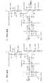
[発光装置10]
図1は、発光装置10の等価回路図である。図1では、以下に説明するダイオード、サイリスタ、抵抗などを、一般的に用いられる記号で示す。他の図面でも同様である。また、図1において、例えば接地電位(GND)である基準電位(以下では、基準電位Vsubと表記する。)は、“▽”で示す。なお、サイリスタとは、アノード、カソード、及び少なくとも1つのゲートを有し、アノードとカソードとの間に電圧が印加されている状態で一定以上の電圧がゲートに印加されることによりオン状態となり、又は、一定以上の電圧がゲートに印加されている状態でアノードとカソードとの間に電圧が印加されることによりオン状態となり、保持電流以上の電流がアノードとカソード間に流れている間はオン状態を維持する素子である。[Light emitting device 10]
FIG. 1 is an equivalent circuit diagram of the
発光装置10は、発光部100と制御部110とを備える。
発光部100は、発光素子部101と水平方向転送部102と垂直方向転送部103とを備える。なお、水平方向転送部102を、h方向転送部102と表記し、垂直方向転送部103を、v方向転送部103と表記する。水平方向及び垂直方向については、後述する。
発光素子部101は、発光素子の一例としてレーザ光を出射するレーザダイオードLDを備える。なお、レーザダイオードLDは、例えば垂直共振器面発光レーザVCSEL(Vertical Cavity Surface Emitting Laser)である。発光部100は、後述するように自己走査型発光素子アレイ(SLED:Self-Scanning Light Emitting Device)として構成されている。The
The
The light emitting
図1においては、発光素子部101は、4×4のマトリクス(二次元状)に配列された16個のレーザダイオードLDを備える。なお、二次元状とは、次元の数が二つあることをいい、例えば次に説明する水平方向と垂直方向とに広がっていることをいう。ここで、図1の紙面において、右から左へ向かう方向を水平方向とし、“h”又は“h方向”と表記する。そして、上から下に向かう方向を垂直方向とし、“v”又は“v方向”と表記する。ここでは、h方向とv方向とは、直交するとするが、直交しなくてもよい。 In FIG. 1, the light emitting
発光素子部101は、h方向にレーザダイオードLD11、LD12、LD13、LD14が配列された行、レーザダイオードLD21、LD22、LD23、LD24が配列された行、レーザダイオードLD31、LD32、LD33、LD34が配列された行、レーザダイオードLD41、LD42、LD43、LD44が配列された行を備える。これらの行が、この順でv方向に配列されている。つまり、発光部100は、v方向にレーザダイオードLD11、LD21、LD31、LD41が配列された列、レーザダイオードLD12、LD22、LD32、L42が配列された列、レーザダイオードLD13、LD23、LD33、LD43が配列された列、レーザダイオードLD14、LD24、LD34、LD44が配列された列を備えている。 The light emitting
上記のように、レーザダイオードLDをそれぞれ区別する場合は、「LD11」のように二桁の数字を付す。なお、h方向の数字の代わりに「i」を、v方向の数字の代わりに「j」を付して、「LDji」と表記する場合もある。また、他の場合も同様であるが、h方向のみに数字を付す場合、個々の数字を付す代わりに「i」を、v方向のみに数字を付す場合、個々の数字を付す代わりに「j」を付す場合がある。ここでは、i、jは1〜4の整数である。 As described above, when distinguishing between the laser diodes LD, a two-digit number such as “LD11” is attached. In some cases, "i" is attached instead of the numeral in the h direction, and "j" is attached in place of the numeral in the v direction, to be represented as "LDji". The same applies to other cases. However, when a number is given only in the h direction, “i” is assigned instead of an individual number, and when a number is assigned only in the v direction, “j” is assigned instead of an individual number. May be appended. Here, i and j are integers of 1 to 4.
そして、発光素子部101は、16個の駆動サイリスタBと16個の駆動サイリスタUとさらに備える。各駆動サイリスタB、Uは、各レーザダイオードLDと接続されている。ここでは、レーザダイオードLD、駆動サイリスタB、駆動サイリスタUの順となるように、各レーザダイオードLDと各駆動サイリスタB、Uとが直列接続されている。つまり、レーザダイオードLD、駆動サイリスタB及び駆動サイリスタUが組を構成している。よって、駆動サイリスタB、Uには、接続されるレーザダイオードLDと同じ数字を付して、それぞれを区別する。 Further, the light emitting
本明細書では、「〜」は、番号によってそれぞれが区別された複数の構成要素を示すもので、「〜」の前後に記載されたもの及びその間の番号のものを含むことを意味する。例えば、レーザダイオードLD11〜14は、レーザダイオードLD11から番号順にレーザダイオードLD14までを含む。 In this specification, “to” indicates a plurality of components that are each distinguished by a number, and includes those described before and after “to” and those with numbers between them. For example, the laser diodes LD11 to LD14 include the laser diode LD11 to the laser diode LD14 in numerical order.
h方向転送部102は、4個の転送サイリスタThと、4個の結合ダイオードDhと、4個の接続ダイオードDaと、4個の抵抗Rhとを備える。さらに、h方向転送部102は、スタートダイオードDhsを備える。 The h-
転送サイリスタThは、h方向に転送サイリスタTh1、Th2、Th3、Th4の順で配列されている。そして、結合ダイオードDhは、h方向に結合ダイオードDh1、Dh2、Dh3、Dh4の順で配列されている。なお、結合ダイオードDh1、Dh2、Dh3は、転送サイリスタTh1、Th2、Th3、Th4の各間に設けられ、結合ダイオードDh4は、転送サイリスタTh4の結合ダイオードDh3が設けられた側と反対側に設けられている。接続ダイオードDa及び抵抗Rhも、同様にh方向に配列されている。
転送サイリスタTh、結合ダイオードDh、接続ダイオードDa、抵抗Rhは、h方向に配列されているので、一桁の数字が付される。なお、個々の数字を付す代わりに「i」を付す場合がある。The transfer thyristors Th are arranged in the h direction in the order of the transfer thyristors Th1, Th2, Th3, and Th4. The coupling diodes Dh are arranged in the h direction in the order of the coupling diodes Dh1, Dh2, Dh3, and Dh4. The coupling diodes Dh1, Dh2, and Dh3 are provided between the transfer thyristors Th1, Th2, Th3, and Th4, and the coupling diode Dh4 is provided on the side of the transfer thyristor Th4 that is opposite to the side on which the coupling diode Dh3 is provided. ing. The connection diode Da and the resistor Rh are also arranged in the h direction.
Since the transfer thyristor Th, the coupling diode Dh, the connection diode Da, and the resistor Rh are arranged in the h direction, they are denoted by single-digit numbers. Note that “i” may be added instead of individual numbers.
v方向転送部103は、4個の転送サイリスタTvと、4個の結合ダイオードDvと、4個の設定サイリスタSと、4個の接続ダイオードDbと、4個の接続抵抗Rcと、4個の抵抗Rvとを備える。さらに、v方向転送部103は、スタートダイオードDvsを備える。 The v-
転送サイリスタTvは、v方向に転送サイリスタTv1、Tv2、Tv3、Tv4の順で配列されている。そして、結合ダイオードDvは、v方向に結合ダイオードDv1、Dv2、Dv3、Dv4の順で配列されている。なお、結合ダイオードDv1、Dv2、Dv3は、転送サイリスタTv1、Tv2、Tv3、Tv4の各間に設けられ、結合ダイオードDv4は、転送サイリスタTv4の結合ダイオードDv3が設けられた側と反対側に設けられている。
設定サイリスタSは、v方向に設定サイリスタS1、S2、S3、S4の順で配列されている。
接続ダイオードDb、接続抵抗Rc及び抵抗Rvも、同様にv方向に配列されている。
転送サイリスタTv、結合ダイオードDv、設定サイリスタS、接続ダイオードDb、接続抵抗Rc及び抵抗Rvは、v方向に配列されているので、一桁の数字が付される。なお、個々の数字を付す代わりに「j」を付す場合がある。The transfer thyristors Tv are arranged in the v direction in the order of the transfer thyristors Tv1, Tv2, Tv3, and Tv4. The coupling diodes Dv are arranged in the v direction in the order of the coupling diodes Dv1, Dv2, Dv3, and Dv4. The coupling diodes Dv1, Dv2, Dv3 are provided between the transfer thyristors Tv1, Tv2, Tv3, Tv4, and the coupling diode Dv4 is provided on the side of the transfer thyristor Tv4 opposite to the side on which the coupling diode Dv3 is provided. ing.
The setting thyristors S are arranged in the v direction in the order of the setting thyristors S1, S2, S3, and S4.
The connection diode Db, the connection resistance Rc, and the resistance Rv are similarly arranged in the v direction.
Since the transfer thyristor Tv, the coupling diode Dv, the setting thyristor S, the connection diode Db, the connection resistance Rc, and the resistance Rv are arranged in the v direction, a single-digit number is assigned. Note that "j" may be added instead of individual numbers.
レーザダイオードLD、結合ダイオードDh、Dv及び接続ダイオードDa、Dbは、アノードとカソードとを備える2端子素子である。
転送サイリスタTh、Tv、設定サイリスタS及び駆動サイリスタU、Bは、アノード、カソード、ゲートを備える3端子素子である。
ここで、転送サイリスタThは、第1の転送素子の一例であり、転送サイリスタTvは、第2の転送素子の一例である。駆動サイリスタUは、第1の駆動素子の一例及び第1のサイリスタの一例であり、駆動サイリスタBは、第2の駆動素子の一例及び第2のサイリスタの一例である。設定サイリスタSは、設定素子の一例である。The laser diode LD, the coupling diodes Dh and Dv, and the connection diodes Da and Db are two-terminal elements having an anode and a cathode.
The transfer thyristors Th and Tv, the setting thyristor S, and the drive thyristors U and B are three-terminal elements having an anode, a cathode, and a gate.
Here, the transfer thyristor Th is an example of a first transfer element, and the transfer thyristor Tv is an example of a second transfer element. The drive thyristor U is an example of a first drive element and an example of a first thyristor, and the drive thyristor B is an example of a second drive element and an example of a second thyristor. The setting thyristor S is an example of a setting element.
次に、上記の各素子(レーザダイオードLD、駆動サイリスタU、B、転送サイリスタTh、Tvなど)の接続関係を説明する。
前述したように、レーザダイオードLDjiと駆動サイリスタBjiと駆動サイリスタUjiとは直列接続された組を構成する。すなわち、レーザダイオードLDjiのアノードは、基準電位Vsubに接続され、カソードは、駆動サイリスタBjiのアノードに接続されている。駆動サイリスタBjiのカソードは、駆動サイリスタUijのアノードに接続されている。そして、駆動サイリスタUijのカソードは、レーザダイオードLDijに発光のための電流を供給する点灯信号Vonが供給される点灯信号線54に接続されている。Next, a description will be given of the connection relationship between the above-described elements (laser diode LD, drive thyristors U and B, transfer thyristors Th and Tv, and the like).
As described above, the laser diode LDji, the drive thyristor Bji, and the drive thyristor Uji form a series-connected set. That is, the anode of the laser diode LDji is connected to the reference potential Vsub, and the cathode is connected to the anode of the drive thyristor Bji. The cathode of the drive thyristor Bji is connected to the anode of the drive thyristor Uij. The cathode of the driving thyristor Uij is connected to a
つまり、直列接続されたレーザダイオードLDji、駆動サイリスタBji及び駆動サイリスタUjiの組の全ては、レーザダイオードLDjiのアノードが基準電位Vsubに、駆動サイリスタUjiのカソードが点灯信号線54に、並列接続されている。なお、点灯信号線54は、点灯電極の一例である。 In other words, all of the sets of the laser diode LDji, the drive thyristor Bji, and the drive thyristor Uji connected in series have the anode of the laser diode LDji connected to the reference potential Vsub, and the cathode of the drive thyristor Uji connected to the
h方向転送部102において、転送サイリスタThiは、アノードが基準電位Vsubに接続されている。奇数番号の転送サイリスタTh1、Th3は、カソードが転送信号線52に接続されている。転送信号線52には、制御部110から転送信号φh1が供給される。偶数番号の転送サイリスタTh2、Th4は、カソードが転送信号線53に接続されている。転送信号線53には、制御部110から転送信号φh2が供給される。 In the h-
結合ダイオードDhiは、直列接続されている。つまり、一つの結合ダイオードDhのカソードが+h方向に隣接する結合ダイオードDhのアノードに接続されている。そして、結合ダイオードDhiのアノードは、転送サイリスタThiのゲートに接続されている。また、転送サイリスタThiのゲートは、抵抗Rhiを介して、h方向転送部102にh方向電源電位Vgk1が供給される電源線51に接続されている。
スタートダイオードDhsは、アノードが転送信号φh2の供給される転送信号線53に接続され、カソードが結合ダイオードDh1のアノードに接続されている。The coupling diodes Dhi are connected in series. That is, the cathode of one coupling diode Dh is connected to the anode of the coupling diode Dh adjacent in the + h direction. The anode of the coupling diode Dhi is connected to the gate of the transfer thyristor Thi. Further, the gate of the transfer thyristor Thi is connected to the
The start diode Dhs has an anode connected to the
そして、接続ダイオードDaiは、アノードが転送サイリスタThiのゲートに接続され、カソードが駆動サイリスタUji(j=1〜4)のゲートに並列接続されている。 The connection diode Dai has an anode connected to the gate of the transfer thyristor Thi and a cathode connected in parallel to the gates of the drive thyristors Uji (j = 1 to 4).
v方向転送部103において、転送サイリスタTvjは、アノードが基準電位Vsubに接続されている。奇数番号の転送サイリスタTv1、Tv3は、カソードが転送信号線62に接続されている。転送信号線62には、制御部110から転送信号φv1が供給される。偶数番号の転送サイリスタTv2、Tv4は、カソードが転送信号線63に接続されている。転送信号線63には、制御部110から転送信号φv2が供給される。 In the v-
結合ダイオードDvjは、直列接続されている。つまり、一つの結合ダイオードDvのカソードが+v方向に隣接する結合ダイオードDvのアノードに接続されている。そして、結合ダイオードDvjのアノードは、転送サイリスタTvjのゲートに接続されている。また、転送サイリスタTvjのゲートは、抵抗Rvjを介して、v方向転送部103にv方向電源電位Vgk2が供給される電源線61に接続されている。
スタートダイオードDvsは、アノードが転送信号φv2の供給される転送信号線63に接続され、カソードが結合ダイオードDv1のアノードに接続されている。The coupling diodes Dvj are connected in series. That is, the cathode of one coupling diode Dv is connected to the anode of the coupling diode Dv adjacent in the + v direction. The anode of the coupling diode Dvj is connected to the gate of the transfer thyristor Tvj. The gate of the transfer thyristor Tvj is connected to a
The start diode Dvs has an anode connected to the
設定サイリスタSjは、アノードが基準電位Vsubに接続され、カソードが制御部110から設定信号φsが供給される設定信号線64に接続されている。 The setting thyristor Sj has an anode connected to the reference potential Vsub and a cathode connected to the
そして、接続ダイオードDbjは、アノードが転送サイリスタTvjのゲートに接続され、カソードが設定サイリスタSjのゲートに接続されている。 The connection diode Dbj has an anode connected to the gate of the transfer thyristor Tvj and a cathode connected to the gate of the setting thyristor Sj.
さらに、接続抵抗Rcjは、一方が設定サイリスタSjのゲートに接続され、他方が駆動サイリスタBji(i=1〜4)のゲートに並列接続されている。 Further, one of the connection resistors Rcj is connected to the gate of the setting thyristor Sj, and the other is connected in parallel to the gate of the driving thyristor Bji (i = 1 to 4).
制御部110の構成を説明する。
制御部110は、h方向転送信号生成部120と、v方向転送信号生成部130と、設定信号生成部140と、点灯信号生成部150と、基準電位生成部160と、h方向電源電位生成部170と、v方向電源電位生成部180とを備える。制御部110は、電子回路で構成されている。例えば、制御部110は、集積回路(IC)として構成されていてもよい。The configuration of the
The
h方向転送信号生成部120は、転送信号φh1、φh2を生成し、それぞれを発光部100の転送信号線52、53に供給する。v方向転送信号生成部130は、転送信号φv1、φv2を生成し、それぞれを発光部100の転送信号線62、63に供給する。
設定信号生成部140は、設定信号φsを生成し、発光部100の設定信号線64に供給する。The h-direction
The setting
なお、h方向転送信号生成部120と転送信号線52、53との間には、不図示の電流制限抵抗がそれぞれ設けられ、転送信号線52、53の電位の変動が、h方向転送信号生成部120に及ばないようになっている。v方向転送信号生成部130と転送信号線62、63との間、及び、設定信号生成部140と設定信号線64との間も同様である。つまり、転送信号線52、53の電位は、転送サイリスタThの動作状態、つまりオン状態又はオフ状態により電変動する。同様に、転送信号線62、63の電位は、転送サイリスタTvの動作状態、つまりオン状態又はオフ状態により電変動する。
これらの制限抵抗は、発光部100に設けられてもよく、制御部110に設けられてもよい。また、これらの制限抵抗は、発光部100と制御部110との間に設けられてもよい。Note that current limiting resistors (not shown) are provided between the h-direction transfer
These limiting resistances may be provided in the
点灯信号生成部150は、点灯信号Vonを生成し、発光部100の点灯信号線54に供給する。 The lighting
基準電位生成部160は、基準電位Vsubを生成し、発光部100に供給する。
h方向電源電位生成部170は、h方向電源電位Vgk1を生成し、発光部100の電源線51に供給する。v方向電源電位生成部180は、v方向電源電位Vgk2を生成し、発光部100の電源線61に供給する。The reference
The h-direction power supply
h方向転送信号生成部120、v方向転送信号生成部130、設定信号生成部140及び点灯信号生成部150の生成する信号と、基準電位生成部160、h方向電源電位生成部170及びv方向電源電位生成部180の生成する電位については、後述する。
発光部100は、供給された信号及び電位によって動作する。The signals generated by the h-direction
The
以上においては、発光部100は、レーザダイオードLDが4×4の二次元的に配置されているとしたが、4×4に限定されない。i×jにおけるi及び/又はjは、4以外の複数の数値であってもよい。そして、h方向転送部102に含まれる転送サイリスタThなどの数は、iであればよい。また、v方向転送部103に含まれる転送サイリスタTv、設定サイリスタSなどの数は、jであればよい。なお、転送サイリスタThなどの数は、iを超える数であってもよいし、iより少ない数であってもよい。同様に、転送サイリスタTv、設定サイリスタSなどの数は、jを超える数であってもよいし、jより少ない数であってもよい。 In the above description, the
なお、図1では、発光部100において、制御部110からの信号及び電位が供給される線との接続部分に符号を付していない。なお、接続部分は、“□”で表記している。しかし、以下に示す図においては、制御部110が供給する信号又は電位に端子を付して表記することがある。例えば、h方向転送信号生成部120から転送信号φh1が供給される接続部分を、“φh1端子”と表記する。 Note that, in FIG. 1, in the
(発光部100)
発光部100は、レーザ光を出射しうる半導体材料で構成される。例えば、発光部100は、GaAs系の化合物半導体で構成されている。ここでは、後述する発光部100の断面図(後述する図3(a)、(b)、図5(a)、(b)参照)に示すように、p型のGaAsで構成された基板80上に、GaAs系の化合物半導体層が複数積層された半導体層積層体にて構成されている。そして、基板80は、基板80の裏面に形成された裏面電極99を介して供給される基準電位Vsubに設定されている。まず、平面レイアウトを説明する。なお、裏面電極99は、基準電極の一例である。(Light emitting unit 100)
The
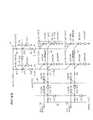
図2は、発光部100の平面レイアウトの一例を示す図である。
発光部100は、前述した半導体層積層体がメサエッチングにより素子間分離された複数のアイランドで構成されている。ここでは、図2に示すアイランド301〜308により、発光部100の平面レイアウトを説明する。FIG. 2 is a diagram illustrating an example of a planar layout of the
The
アイランド301には、駆動サイリスタU11と駆動サイリスタB11とレーザダイオードLD11とが設けられている。駆動サイリスタU11と駆動サイリスタB11とレーザダイオードLD11とは、積層されて直列接続されている。図2では、駆動サイリスタU11と駆動サイリスタB11とレーザダイオードLD11とを、U/B/LD11と表記する。なお、後述するように、基板80側からレーザダイオードLD11、駆動サイリスタB11、駆動サイリスタU11の順で積層されている。つまり、駆動サイリスタU11は上側、駆動サイリスタB11は下側にある。以下では、駆動サイリスタU11と駆動サイリスタB11とレーザダイオードLD11との直列接続を、駆動サイリスタU/駆動サイリスタB/レーザダイオードLD又はU/B/LDと表記する。積層された駆動サイリスタU/駆動サイリスタB/レーザダイオードLDは、発光デバイスの一例である。
アイランド301と同様なアイランドに、iが2〜4でjが2〜4のレーザダイオードLDjiと駆動サイリスタBjiと駆動サイリスタUjiとの組が構成されている。
なお、駆動サイリスタU11と駆動サイリスタB11とレーザダイオードLD11とは、積層によらないで、直列接続されていてもよい。The
In an island similar to the
The drive thyristor U11, the drive thyristor B11, and the laser diode LD11 may be connected in series without being stacked.
アイランド302には、転送サイリスタTh1と結合ダイオードDh1と接続ダイオードDa1とが設けられている。アイランド302と同様なアイランドに、iが2〜4の転送サイリスタThiと結合ダイオードDhiと接続ダイオードDaiとが設けられている。 The
アイランド303には、抵抗Rh1が設けられている。アイランド303と同様なアイランドに、iが2〜4の抵抗Rhiが設けられている。
アイランド304には、スタートダイオードDhsが設けられている。The island Rh is provided with a resistor Rh1. In an island similar to the
The
アイランド305には、転送サイリスタTv1と結合ダイオードDv1と接続ダイオードDb1とが設けられている。アイランド305と同様なアイランドに、jが2〜4の転送サイリスタTvjと結合ダイオードDvjと接続ダイオードDbjとが設けられている。 The
アイランド306には、設定サイリスタS1と接続抵抗Rc1とが設けられている。アイランド306と同様なアイランドに、jが2〜4の設定サイリスタSjと接続抵抗Rcjとが設けられている。 The
アイランド307には、抵抗Rv1が設けられている。アイランド307と同様なアイランドに、jが2〜4の抵抗Rhjが設けられている。
アイランド308には、スタートダイオードDvsが設けられている。The
The
接続関係などの詳細は、後述する発光素子部101、h方向転送部102、v方向転送部103の断面構造と合わせて説明する。
なお、図2においては、後述する配線とアイランドとの接続点に設けられるスルーホールを〇で示している。Details such as the connection relationship will be described together with the cross-sectional structure of the light emitting
In FIG. 2, a through hole provided at a connection point between a wiring and an island, which will be described later, is indicated by a triangle.
次に、発光素子部101の断面構造を説明する。
図3は、駆動サイリスタU/駆動サイリスタB/レーザダイオードLDの断面図である。図3(a)は、図2におけるIIIA−IIIA線での断面図、図3(b)は、図2におけるIIIB−IIIB線での断面図である。つまり、図3(a)においては、U/B/LD11、U/B/LD12、U/B/LD13及びU/B/LD14が記載されている。図3(b)には、U/B/LD11、U/B/LD21、U/B/LD31及びU/B/LD41が記載されている。Next, a cross-sectional structure of the light emitting
FIG. 3 is a sectional view of the drive thyristor U / drive thyristor B / laser diode LD. 3A is a sectional view taken along the line IIIA-IIIA in FIG. 2, and FIG. 3B is a sectional view taken along the line IIIB-IIIB in FIG. That is, FIG. 3A illustrates U / B / LD11, U / B / LD12, U / B / LD13, and U / B / LD14. FIG. 3B shows U / B / LD11, U / B / LD21, U / B / LD31, and U / B / LD41.
図3(a)の駆動サイリスタU11/駆動サイリスタB11/レーザダイオードLD11(図中においては、U/B/LD11と表記)の断面に示すように、p型のGaAsの基板80上に、レーザダイオードLD11を構成するp型のアノード層(以下では、pアノード層と表記する。以下同様である。)81、発光層82、n型のカソード層(nカソード層)83が積層されている。そして、nカソード層83上に、トンネル接合層84が積層されている。そして、トンネル接合層84上に、駆動サイリスタB11を構成するp型のアノード層(pアノード層)85、電圧低減層86、n型のゲート層(nゲート層)87、p型のゲート層(pゲート層)88、n型のカソード層(nカソード層)89が設けられている。さらに、nカソード層89上に、トンネル接合層90が積層されている。そして、トンネル接合層90上に、駆動サイリスタU11を構成するp型のアノード層(pアノード層)91、電圧低減層92、n型のゲート層(nゲート層)93、p型のゲート層(pゲート層)94、n型のカソード層(nカソード層)95が設けられている。そして、これらの半導体層積層体がメサエッチングにより分離されている。 As shown in the cross section of the drive thyristor U11 / drive thyristor B11 / laser diode LD11 (denoted as U / B / LD11 in the figure) in FIG. 3A, a laser diode is provided on a p-
以上説明したように、レーザダイオードLD11は、pアノード層81、発光層82及びnカソード層83により構成されている。駆動サイリスタB11は、pアノード層85、電圧低減層86、nゲート層87、pゲート層88及びnカソード層89により構成されている。そして、駆動サイリスタU11は、pアノード層91、電圧低減層92、nゲート層93、pゲート層94及びnカソード層95により構成されている。
そして、レーザダイオードLD11と駆動サイリスタB11とが、トンネル接合層84を介して積層され、駆動サイリスタB11と駆動サイリスタU11とが、トンネル接合層90を介して積層されている。As described above, the laser diode LD11 includes the
The laser diode LD11 and the drive thyristor B11 are stacked via a
そして、レーザダイオードLDのpアノード層81には、電流狭窄層が含まれている。電流狭窄層とは、レーザダイオードLDに流れる電流の経路を狭窄する層である。電流狭窄層には、例えば、AlAsのように、酸化によりAl2O3が形成されることで、電気抵抗が高くなる層が用いられる。この場合、メサエッチングにより露出した部分(周辺部)から酸化を進め、中央部は酸化されないようにすることができる。すると、中央部が、電流が流れやすい領域(電流通過領域α)となり、酸化された周辺部が、電流が流れにくい領域(電流阻止領域β)となる。メサエッチングに起因した欠陥が多い周辺部は、非発光再結合が起こりやすい。よって、周辺部を電流阻止領域βとすることで、非発光再結合に消費される電力が抑制され、低消費電力化及び光取り出し効率の向上が図れる。なお、光取り出し効率とは、電力当たりに取り出すことができる光量である。The p-
ここでは、レーザダイオードLDの出射する光は、駆動サイリスタB、Uを透過して、基板80と反対側から出射するとしている。図3(a)、(b)では、出射する光を矢印で示している。そして、図3(a)のU/B/LD11における中央部が光出射口γである。 Here, the light emitted from the laser diode LD passes through the drive thyristors B and U, and is emitted from the side opposite to the
そして、図3(a)、(b)に示すように、点灯信号線54は、駆動サイリスタU11のnカソード層95上の一部に設けられたnオーミック電極331に接続されている。
また、図3(a)のU/B/LD11に示すように、hゲート信号線55は、駆動サイリスタUのpゲート層94上に設けられたpオーミック電極352に接続されている。つまり、アイランド301の積層半導体層の一部において、厚さ方向にnカソード層95を除去して、pゲート層94の表面を露出させ、露出したpゲート層94にpオーミック電極352を設けて、hゲート信号線55を接続している。ここで、pゲート層94上に設けられたpオーミック電極352を、駆動サイリスタU11のゲート端子又はゲートと表記することがある。なお、pゲート層94を駆動サイリスタU11のゲートと表記することがある。pオーミック電極352又はpゲート層94が第1のゲートの一例である。Then, as shown in FIGS. 3A and 3B, the
Further, as shown by the U / B /
また、図3(b)のU/B/LD11示すように、vゲート信号線65は、駆動サイリスタUのpゲート層88上に設けられたpオーミック電極351に接続されている。つまり、アイランド301の積層半導体層の一部において、厚さ方向にnカソード層95、pゲート層94、nゲート層93、電圧低減層92、pアノード層91、トンネル接合層90及びnカソード層89を除去して、pゲート層88の表面を露出させ、露出したpゲート層88にpオーミック電極351を設けて、vゲート信号線65を接続している。ここで、pゲート層88上に設けられたpオーミック電極351を、駆動サイリスタB11のゲート端子又はゲートと表記することがある。なお、pゲート層88を駆動サイリスタB11のゲートと表記することがある。pオーミック電極351又はpゲート層88が第2のゲートの一例である。 Further, as shown by U / B /
上記の接続する部分を除いて、アイランド301、vゲート信号線65、hゲート信号線55及び点灯信号線54のそれぞれの間は、絶縁層96、97、98を介して絶縁されている。つまり、アイランド301の表面が、絶縁層96で覆われている。そして、絶縁層96上にvゲート信号線65が形成されている。絶縁層96により、アイランド301を構成する積層半導体層とvゲート信号線65とが絶縁されている。次に、vゲート信号線65上に絶縁層97が設けられている。そして、絶縁層97上にhゲート信号線55が設けられている。つまり、絶縁層97により、vゲート信号線65とhゲート信号線55とが絶縁されている。そして、hゲート信号線55上に絶縁層98が設けられている。絶縁層98上に点灯信号線54が設けられている。つまり絶縁層98により、hゲート信号線55と点灯信号線54とが絶縁されている。このようにして、hゲート信号線55とvゲート信号線65と点灯信号線54とが互いに絶縁されている。他の、hゲート信号線56〜58、vゲート信号線66〜68も同様である。 Except for the connection portions described above, the
図4は、上側の駆動サイリスタU11/下側の駆動サイリスタB11/レーザダイオードLD11を備えるアイランド301の拡大平面図である。ここでは、駆動サイリスタU11/駆動サイリスタB11/レーザダイオードLD11で説明するが、他の駆動サイリスタB/駆動サイリスタU/レーザダイオードLDも同様である。図4では、アイランド301に加え、hゲート信号線55、vゲート信号線65及び点灯信号線54を示している。なお、点灯信号線54は、下部の構造を見やすくするために、破線で示している。また、図4では、vゲート信号線65が−h方向につながっていないが、他の駆動サイリスタB/駆動サイリスタU/レーザダイオードLDでは、−h方向につながっている場合がある。同様に、図4では、hゲート信号線55が+v方向につながっているが、+v方向につながっていない場合がある(図2参照)。 FIG. 4 is an enlarged plan view of the
図4に示すように、アイランド301は、表面の外形が円形であって、中央部が光を出射する円形の光出射口γとなっている。なお、アイランド301の表面の外形は、平面形状は、円形でなくてもよく、四角形状、四角形を超える多角形など他の形状であってもよい。光出射口γの平面形状も同様である。 As shown in FIG. 4, the
そして、アイランド301は、周辺部の一部において、厚さ方向にnカソード層95が除去されて、pゲート層94が露出している。露出したpゲート層94上にp型の半導体層に対してオーミック接触しやすいpオーミック電極352が設けられている。そして、pオーミック電極352にhゲート信号線55が接続されている。
同様に、アイランド301は、周辺部の他の一部において、厚さ方向にnカソード層95、pゲート層94、nゲート層93、電圧低減層92、pアノード層91、トンネル接合層90、nカソード層89が除去されて、pゲート層88が露出している。露出したpゲート層88上にp型の半導体層に対してオーミック接触しやすいpオーミック電極351が設けられている。そして、pオーミック電極351にvゲート信号線65が接続されている。In the
Similarly, the
さらに、アイランド301において、残されたnカソード層95で構成されるn領域311において、nカソード層95上にU字状にn型の半導体層に対してオーミック接触しやすいnオーミック電極331が設けられている。そして、nオーミック電極331に点灯信号線54が接続されている。
なお、pオーミック電極351、352及びnオーミック電極331は、光出射口γを取り囲むように構成されている。そして、光の出射が妨げられないように、hゲート信号線55、vゲート信号線65及び点灯信号線54は、光出射口γを覆わないに設けられている。Further, in the
The p-
前述したように、アイランド301、hゲート信号線55、vゲート信号線65及び点灯信号線54は、絶縁層96、97、98により互いに短絡することがないように構成されている。なお、絶縁層96、97、98に設けられたスルーホールは、便宜的に円で示しているが、他の形状であってもよい。 As described above, the
なお、図3(a)、(b)において示したように、レーザダイオードLDが出射する光は、駆動サイリスタB及び駆動サイリスタUを透過して出射される。その他の実施例として、レーザダイオードLDが出射する光が通過する位置(光出射口γ)に繋がる駆動サイリスタB、Uの一部又はすべてを除去してもよい。このようにして、駆動サイリスタB、Uによる光吸収を低減もしくは無くしてもよい。または、レーザダイオードLDが出射する光の方向を、基板80側(裏面出射)としてもよい。 Note that, as shown in FIGS. 3A and 3B, the light emitted from the laser diode LD passes through the drive thyristor B and the drive thyristor U and is emitted. As another embodiment, some or all of the drive thyristors B and U connected to the position (light emission port γ) through which the light emitted from the laser diode LD passes may be removed. In this way, light absorption by the drive thyristors B and U may be reduced or eliminated. Alternatively, the direction of the light emitted from the laser diode LD may be set to the
図5は、h方向転送部102の転送サイリスタTh1、結合ダイオードDh1及び接続ダイオードDa1を含むアイランド302と、v方向転送部103の転送サイリスタTv1、結合ダイオードDv1及び接続ダイオードDb1を含むアイランド305と、設定サイリスタS1及び接続抵抗Rc1を含むアイランド306の断面図である。図5(a)は、図2のVA−VA線でのアイランド302の断面図、図5(b)は、図2のVB−VB線でのアイランド305及びアイランド306の断面図である。 FIG. 5 shows an
まず、図5(a)に示すアイランド302を説明する。
アイランド302は、v方向に結合ダイオードDh1、転送サイリスタTh1及び接続ダイオードDa1を備える。
そして、アイランド302は、アイランド301におけるレーザダイオードLD11を構成するpアノード層81、発光層82、nカソード層83と、駆動サイリスタB11を構成するpアノード層85、電圧低減層86、nゲート層87、pゲート層88、nカソード層89と、nカソード層83とpアノード層85との間に設けられたトンネル接合層84とを備える。つまり、アイランド302は、アイランド301が備えた駆動サイリスタUを構成するpアノード層91、電圧低減層92、nゲート層93、pゲート層94、nカソード層95、及び、nカソード層89とpアノード層91との間に設けられたトンネル接合層90を備えない。
つまり、半導体層積層体において、トンネル接合層90、pアノード層91、電圧低減層92、nゲート層93、pゲート層94及びnカソード層95が除去されている。
そして、アイランド302の周囲には、基板80が露出している。First, the
The
The
That is, in the semiconductor layer laminate, the
The
転送サイリスタTh1は、nカソード層89、pゲート層88、nゲート層87、電圧低減層86及びpアノード層85により構成されている。つまり、nカソード層89がカソード、pゲート層88がゲート、pアノード層85がアノードとなっている。そして、nカソード層89で構成されたn領域313上に設けられたnオーミック電極333がカソード端子となって、転送信号線52に接続されている。nカソード層89を除去して露出させたpゲート層88上に設けられたpオーミック電極353(図2参照)がゲート端子となって、アイランド303に設けられた抵抗Rh1の一方の端子(図2に示す符号なしのpオーミック電極)に接続されるとともに、スタートダイオードDhsのアノード端子であるpオーミック電極354に接続されている。 The transfer thyristor Th1 includes an
さらに、アイランド302の一部は、厚さ方向にnカソード層89、pゲート層88、nゲート層87及び電圧低減層86が除去されて、pアノード層85を露出させている。露出させたpアノード層85と露出させた基板80とが、pオーミック電極71により接続されている。つまり、転送サイリスタTh1のアノードであるpアノード層85には、基準電位Vsubが印加される。そして、レーザダイオードLDを構成するpアノード層81、発光層82及びnカソード層83は、pオーミック電極71により短絡されて、発光することがない。
なお、カソード端子となるnオーミック電極333、ゲート端子となるpオーミック電極353が設けられない場合がある。よって、転送サイリスタThにおいて、nカソード層89をカソード、pゲート層88をゲート、pアノード層85をアノードと表記することがある。後述する転送サイリスタTv及び設定サイリスタSにおいても同様である。Further, in a part of the
Note that the n-
図5(a)においては、pオーミック電極71を結合ダイオードDh1に隣接した部分に記載した。しかし、図2に示すように、アイランド302、303、これらと同様のアイランド及びアイランド304において、厚さ方向にnカソード層89、pゲート層88、nゲート層87及び電圧低減層86をメサエッチングしてアイランド間を素子分離し、pアノード層85、トンネル接合層84、nカソード層83、発光層82及びpアノード層81を残してもよい。この場合には、図2に示したように、基板80とpアノード層85とを接続するpオーミック電極71が共通に設けられる。つまり、pオーミック電極71を設ける領域が小さくなる。 In FIG. 5A, the
結合ダイオードDh1は、nカソード層89とpゲート層88とにより構成されている。つまり、結合ダイオードDh1は、nカソード層89で構成されたn領域314上に設けられたnオーミック電極334がカソード端子となって、配線60に接続されている。配線60は、アイランド302と同様な隣接するアイランドにおける転送サイリスタTh2のゲート端子(アイランド302のpオーミック電極353と同様なゲート端子)に接続されている(図2参照)。 The coupling diode Dh1 includes an
一方、結合ダイオードDh1は、pゲート層88上に設けられたpオーミック電極353がアノード端子となって、アイランド303に設けられた抵抗Rh1の一方の端子(図2に示す符号なしのpオーミック電極)に接続される。なお、結合ダイオードDh1のアノードとなるpゲート層88は、転送サイリスタTh1のpゲート層88と共通である。つまり、pゲート層88を介して、結合ダイオードDh1のアノードと、転送サイリスタTh1のゲートとが、接続されている。
なお、カソード端子となるnオーミック電極334及びアノード端子となるpオーミック電極353が設けられない場合がある。よって、結合ダイオードDhにおいて、nカソード層89をカソード、pゲート層88をアノードと表記することがある。後述する結合ダイオードDv及び接続ダイオードDa、Dbにおいても同様である。On the other hand, the coupling diode Dh1 is configured such that the p-
In some cases, the
接続ダイオードDa1は、結合ダイオードDh1と同様にnカソード層89とpゲート層88とにより構成されている。つまり、接続ダイオードDa1は、nカソード層89で構成されたn領域312上に設けられたnオーミック電極332がアノード端子となって、配線55に接続されている。一方、接続ダイオードDa1のアノードとなるpゲート層88は、転送サイリスタTh1のpゲート層88と共通であって、pゲート層88を介して、接続ダイオードDa1のアノードと、転送サイリスタTh1のゲートとに接続されている。配線55は、アイランド301に設けられた駆動サイリスタU11のゲートに接続されている(図3(a)参照)。 The connection diode Da1 includes an n-
なお、図示していないが、抵抗Rh1が設けられるアイランド303では、nカソード層89を除去して露出させたpゲート層88上に設けた一組のpオーミック電極(符号なし)の間のpゲート層88を抵抗に用いる。そして、一方のpオーミック電極がアイランド302に設けられた転送サイリスタTh1のゲートであるpオーミック電極353に接続されている。他方のpオーミック電極が電源線51に接続されている。 Although not shown, in the
同様に、図示していないが、スタートダイオードDhsが設けられるアイランド304でも同様である。つまり、nカソード層89で構成されるn領域315上に設けられたnオーミック電極335が転送信号線53に接続されている。nカソード層89を除去して露出させたpゲート層88上に設けたpオーミック電極354が配線59に接続されている。配線59は、アイランド302に設けられた転送サイリスタTh1のゲートであるpオーミック電極353に接続されている。 Similarly, although not shown, the same applies to the
次に、図5(b)に示すアイランド305、306を説明する。
アイランド305は、h方向に接続ダイオードDb1、転送サイリスタTv1及び結合ダイオードDv1を備える。アイランド305の構成は、アイランド302と同様であるので詳細な説明を省略する。なお、抵抗Rv1が設けられるアイランド307及びスタートダイオードDvsが設けられるアイランド308も同様であるので説明を省略する。Next, the
The
アイランド306は、h方向に接続抵抗Rc1及び設定サイリスタS1を備える。設定サイリスタS1は、転送サイリスタTh1と同様に、nカソード層89、pゲート層88、nゲート層87、電圧低減層86及びpアノード層85により構成されている。つまり、nカソード層89がカソード、pゲート層88がゲート、pアノード層85がアノードとなっている。そして、nカソード層89で構成されたn領域319上に設けられたnオーミック電極339がカソード端子となって、設定信号線64に接続されている。nカソード層89を除去して露出させたpゲート層88上に設けられたpオーミック電極356がゲート端子となって、配線69に接続されている。そして、配線69は、アイランド305の接続ダイオードDb1のnカソード層89で構成されたn領域316上に設けられたカソード端子であるnオーミック電極336に接続されている。つまり、接続ダイオードDb1のカソードと設定サイリスタS1のゲートとが配線69により接続されている。 The
また、アイランド306において、nカソード層89を除去して露出させたpゲート層88上に設けられたpオーミック電極357がvゲート信号線65に接続されている。つまり、アイランド306において、設定サイリスタS1の部分からpオーミック電極357までのpゲート層88が抵抗として機能して、接続抵抗Rc1を構成する。 In the
なお、アイランド305の一部は、厚さ方向にnカソード層89、pゲート層88、nゲート層87及び電圧低減層86が除去されて、pアノード層85を露出させている。そして、露出させたpアノード層85と露出させた基板80とが、pオーミック電極72により接続されている。なお、アイランド305とアイランド306とは、厚さ方向にnカソード層89、pゲート層88、nゲート層87及び電圧低減層86が除去されることで、素子分離されている。つまり、pアノード層85は、アイランド305とアイランド306とで共通である。よって、アイランド305、306のpアノード層85は、基準電位Vsubが供給される。そして、レーザダイオードLDを構成するpアノード層81、発光層82、nカソード層83は、pオーミック電極72により短絡されて、発光することがない。
なお、他のアイランドも同様である。Note that the
The same applies to other islands.
なお、図2に示すように、アイランド305、306、307、これらと同様のアイランドイ及びアイランド308において、厚さ方向にnカソード層89、pゲート層88、nゲート層87及び電圧低減層86を除去してアイランド間を素子分離し、pアノード層85、トンネル接合層84、nカソード層83、発光層82及びpアノード層81を残してもよい。この場合には、図2に示しているように、基板80とpアノード層85とを接続するpオーミック電極72を共通に設ければよい。なお、pオーミック電極71とpオーミック電極72とを共通に設けるように、構成してもよい。 As shown in FIG. 2, in the
以上のように、複数の半導体層を積層した半導体層積層体をメサエッチングにより分離し、一部の層を除去することなどにより、図1に等価回路を示した発光部100が構成される。 As described above, the
<サイリスタ>
次に、サイリスタ(転送サイリスタTh、Tv、設定サイリスタS及び駆動サイリスタU、B)の基本的な動作を説明する。図5(a)に示したように、アイランド302における転送サイリスタTh1のpアノード層85は、基板80に接続されて基準電位Vsubに設定されている。よって、以下では、転送サイリスタTh1をサイリスタの一例として説明する。<Thyristor>
Next, basic operations of the thyristors (the transfer thyristors Th and Tv, the setting thyristor S, and the drive thyristors U and B) will be described. As shown in FIG. 5A, the
図6は、サイリスタの動作を説明する図である。図6(a)は、電圧低減層86を備えない場合、図6(b)は、電圧低減層86を備える場合、図6(c)は、サイリスタ特性である。なお、図6(c)では、電圧を絶対値で示している。また、図6(c)において、電圧低減層86を備えないサイリスタの特性は、「電圧低減層なし」であり、電圧低減層86を備えるサイリスタの特性は、「電圧低減層あり」である。
図5(a)に示すように、転送サイリスタTh1は、pアノード層85、電圧低減層86、nゲート層87、pゲート層88、nカソード層89が積層されて構成されている。そして、pアノード層85は、基準電位Vsubが供給されている。FIG. 6 is a diagram illustrating the operation of the thyristor. 6A shows the case where the
As shown in FIG. 5A, the transfer thyristor Th1 is configured by stacking a p-
さて、図6(a)に示す電圧低減層86を備えないサイリスタは、pアノード層85、nゲート層87、pゲート層88及びnカソード層89が積層されて構成されている。なお、n領域313を除いて、nカソード層89が除去され、pゲート層88が露出している。そして、nカソード層89のn領域313上にnオーミック電極333がカソード端子として設けられ、pゲート層88上にpオーミック電極353がゲート電極として設けられている。
一方、図6(b)に示す電圧低減層86を備えるサイリスタでは、pアノード層85とnゲート層87との間に電圧低減層86を備える。The thyristor without the
On the other hand, the thyristor including the
サイリスタは、前述したように、アノード、カソード、ゲートの3端子を有する半導体素子であって、例えば、GaAs、GaAlAs、AlAsなどによるp型の半導体層(pアノード層85、pゲート層88など)、n型の半導体層(nゲート層87、nカソード層89など)を積層して構成されている。つまり、サイリスタは、pnpn構造を成している。ここでは、p型の半導体層とn型の半導体層とで構成されるpn接合の順方向電位(拡散電位)Vdを一例として1.5Vとして説明する。 As described above, the thyristor is a semiconductor element having three terminals of an anode, a cathode, and a gate. For example, a p-type semiconductor layer of GaAs, GaAlAs, AlAs, or the like (
まず、図6(a)に示す電圧低減層86を備えないサイリスタの動作を説明する。
一例として、pアノード層85の基準電位Vsubをハイレベルの電位(以下では「H」と表記する。)として0V、制御部110におけるh方向電源電位生成部170が供給するh方向電源電位Vgk1をローレベルの電位(以下では「L」と表記する。)として−3.3Vとして説明する。なお、「H(0V)」、「L(−3.3V)」と表記することがある。図1に示したように、h方向電源電位Vgk1が供給される電源線51は、抵抗Rh1を介して、転送サイリスタTh1のゲートに接続されている。First, the operation of the thyristor without the
As an example, the reference potential Vsub of the
アノードとカソードとの間に電流が流れていないオフ状態のサイリスタは、しきい電圧(図6(c)のVs)より低い電位(絶対値が大きい負の電位)がカソードに印加されるとオン状態に移行(ターンオン)する。ここで、サイリスタのしきい電圧は、ゲートの電位からpn接合の順方向電位Vd(1.5V)を引いた値である。
オン状態になると、サイリスタのゲートは、アノードの電位に近い電位になる。ここでは、アノードは0Vであるので、ゲートは、0Vになるとする。また、オン状態のサイリスタのカソードは、アノードの電位からpn接合の順方向電位Vd(1.5V)を引いた電位に近い電位(絶対値を保持電圧と表記する。)となる。ここでは、アノードは0Vであるので、オン状態のサイリスタのカソードは、−1.5Vに近い電位(絶対値が1.5Vより大きい負の電位)となる(図6(c)のVh′)。ここでは、保持電圧は、1.5Vであるとする。A thyristor in an off state in which no current flows between the anode and the cathode is turned on when a potential (a negative potential having a large absolute value) lower than a threshold voltage (Vs in FIG. 6C) is applied to the cathode. Transition to a state (turn on). Here, the threshold voltage of the thyristor is a value obtained by subtracting the forward potential Vd (1.5 V) of the pn junction from the potential of the gate.
When turned on, the gate of the thyristor has a potential close to the potential of the anode. Here, since the anode is at 0V, the gate is assumed to be at 0V. Further, the cathode of the thyristor in the ON state has a potential close to the potential obtained by subtracting the forward potential Vd (1.5 V) of the pn junction from the potential of the anode (the absolute value is referred to as a holding voltage). Here, since the anode is at 0 V, the cathode of the thyristor in the ON state has a potential close to -1.5 V (a negative potential having an absolute value larger than 1.5 V) (Vh 'in FIG. 6C). . Here, it is assumed that the holding voltage is 1.5V.
オン状態のサイリスタは、カソードにオン状態を維持するために必要な電位より低い電位(絶対値が大きい負の電位)が継続的に印加され、オン状態を維持しうる電流(保持電流)が供給されると、オン状態を維持する。
一方、オン状態のサイリスタは、カソードがオン状態を維持するために必要な電位(上記の−1.5Vに近い電位)より高い電位(絶対値が小さい負の電位、0V又は正の電位)になると、オフ状態に移行(ターンオフ)する。In the on-state thyristor, a potential (a negative potential having a large absolute value) lower than a potential necessary for maintaining the on-state is continuously applied to the cathode, and a current (holding current) capable of maintaining the on-state is supplied. Then, the on state is maintained.
On the other hand, the thyristor in the on state has a potential (negative potential, 0 V or positive potential with a small absolute value) higher than the potential (potential close to -1.5 V described above) required for maintaining the cathode in the on state. Then, it shifts to the off state (turns off).
次に、図6(b)に示す電圧低減層86を備える場合のサイリスタの動作について説明する。
サイリスタにおける立ち上がり電圧(図6(c)におけるVr)は、サイリスタを構成する半導体層積層体におけるもっとも小さいバンドギャップのエネルギ(バンドギャップエネルギ)によって決まる。なお、サイリスタにおける立ち上がり電圧Vrとは、図6(c)に示すように、サイリスタのオン状態における電流を、電圧軸に外挿した際の電圧である。Next, the operation of the thyristor provided with the
The rising voltage of the thyristor (Vr in FIG. 6C) is determined by the energy of the smallest band gap (band gap energy) in the semiconductor layer stack constituting the thyristor. The rising voltage Vr in the thyristor is a voltage obtained by extrapolating the current in the ON state of the thyristor to a voltage axis, as shown in FIG.
電圧低減層86は、pアノード層85、nゲート層87、pゲート層88、nカソード層89に比べ、バンドギャップエネルギが小さい層である。よって、電圧低減層86を備えるサイリスタの立ち上がり電圧Vrは、電圧低減層86を備えない図6(a)に示すサイリスタの立ち上がり電圧Vr′に比べて低い。さらに、電圧低減層86は、一例として、発光層82のバンドギャップよりも小さいバンドギャップを有する層である。 The
ここでは、サイリスタ(転送サイリスタTh、Tv、設定サイリスタS、駆動サイリスタB、U)は発光素子として利用されるものではなく、あくまでレーザダイオードLDなどの発光素子を駆動するために設けられている。よって、レーザダイオードLDなどの発光素子の発光波長とは無関係にバンドギャップが決められる。そこで、発光層82のバンドギャップよりも小さいバンドギャップを有する電圧低減層86を設けると、サイリスタの立ち上がり電圧をVr′からVrに低減させられる(Vr′>Vr)。ここでは、サイリスタの立ち上がり電圧Vr、Vr′で説明したが、サイリスタがオン状態を維持する電圧である保持電圧(図6(c)におけるVh、Vh′)も同様である。ここでは、保持電圧は、電圧低減層86を備えない場合の1.5V(Vh′)から電圧低減層86を備える場合には、0.8V(Vh)になるとする。 Here, the thyristors (the transfer thyristors Th and Tv, the setting thyristors S, and the driving thyristors B and U) are not used as light emitting elements, but are provided only for driving light emitting elements such as a laser diode LD. Therefore, the band gap is determined regardless of the emission wavelength of the light emitting element such as the laser diode LD. Therefore, when the
一方、サイリスタのしきい電圧(図6(c)におけるVs)は、逆バイアスになった半導体層の空乏層で決まる。よって、電圧低減層86を設けても、サイリスタのしきい電圧に及ぼす影響が小さい。ここでは、しきい電圧は、電圧低減層86を備えても備えなくとも同じであるとする。なお、しきい電圧は、スイッチング電圧と呼ばれることがある。 On the other hand, the threshold voltage of the thyristor (Vs in FIG. 6C) is determined by the reverse-biased depletion layer of the semiconductor layer. Therefore, even if the
上記において説明したサイリスタの動作は、アノード及びカソードが共に「H」である状態において、カソードに電位が印加された場合の動作である。このとき、ゲートの電位に順方向電位Vdが加えられた電位(絶対値)がカソードに加えられると、サイリスタがターンオンしてオン状態になる。そして、サイリスタのアノードとカソードと間が、保持電圧になる。電圧低減層86を備える場合には、絶対値において0.8Vになる。 The operation of the thyristor described above is an operation when a potential is applied to the cathode in a state where both the anode and the cathode are at “H”. At this time, when a potential (absolute value) obtained by adding the forward potential Vd to the gate potential is applied to the cathode, the thyristor is turned on and turned on. Then, the voltage between the anode and the cathode of the thyristor becomes the holding voltage. When the
一方、カソードとゲートと間が順バイアス状態になって、電流が流れている場合には、アノードとカソードとの間に、保持電圧(絶対値)以上が印加されると、サイリスタはオフ状態からオン状態に移行する。つまり、サイリスタを構成する寄生バイポーラトランジスタ、この場合npnバイポーラトランジスタのベース−エミッタ間が順バイアスになっているために、アノード−カソード間に保持電圧以上の電位が印加されると、サイリスタはオン状態に移行する。電圧低減層86を備えるサイリスタでは、絶対値において0.8Vが印加されればオン状態に移行する。 On the other hand, when a current is flowing between the cathode and the gate in a forward bias state and a holding voltage (absolute value) or more is applied between the anode and the cathode, the thyristor is turned off. Move to ON state. That is, since a parasitic bipolar transistor constituting a thyristor, in this case, a forward bias is applied between the base and the emitter of the npn bipolar transistor, the thyristor is turned on when a potential higher than the holding voltage is applied between the anode and the cathode. Move to The thyristor including the
図7は、半導体層積層体を構成する材料のバンドギャップエネルギを説明する図である。
GaAsの格子定数は、約5.65Åである。AlAsの格子定数は、約5.66Åである。よって、この格子定数に近い材料は、GaAs基板に対してエピタキシャル成長しうる。例えば、GaAsとAlAsとの化合物であるAlGaAsやGeは、GaAs基板に対してエピタキシャル成長しうる。
また、InPの格子定数は、約5.87Åである。この格子定数に近い材料は、InP基板に対してエピタキシャル成長しうる。
また、GaNの格子定数は、成長面によって異なるが、a面が3.19Å、c面が5.17Åである。この格子定数に近い材料はGaN基板に対してエピタキシャル成長しうる。FIG. 7 is a diagram illustrating the band gap energy of the material forming the semiconductor layer stack.
The lattice constant of GaAs is about 5.65 °. The lattice constant of AlAs is about 5.66 °. Therefore, a material having a lattice constant close to this can grow epitaxially on a GaAs substrate. For example, AlGaAs or Ge, which is a compound of GaAs and AlAs, can be epitaxially grown on a GaAs substrate.
The lattice constant of InP is about 5.87 °. Materials near this lattice constant can grow epitaxially on InP substrates.
The lattice constant of GaN depends on the growth plane, but is 3.19 ° for the a-plane and 5.17 ° for the c-plane. Materials near this lattice constant can grow epitaxially on GaN substrates.
そして、GaAs、InP及びGaNに対して、サイリスタの立ち上がり電圧が小さくなる材料は、これら各材料のバンドギャップエネルギよりもバンドギャップエネルギが小さい材料である。一例として、図7に網点で示す範囲の材料である。つまり、網点で示す範囲の材料を、サイリスタを構成する層として用いると、サイリスタの立ち上がり電圧(図6(c)に示すVr)が、網点で示す領域の材料のバンドギャップエネルギになる。
例えば、GaAsのバンドギャップエネルギは、約1.43eVである。よって、電圧低減層86を用いない場合のサイリスタの立ち上がり電圧(図6(c)に示すVr′)は、約1.43Vとなる。しかし、網点で示す範囲の材料を、サイリスタを構成する層とするか、又は、含むことで、サイリスタの立ち上がり電圧(図6(c)に示すVr)は、0V超且つ1.43V未満としうる(0V<Vr<1.43V)。
これにより、サイリスタがオン状態にある時の、電力消費が低減される。A material having a smaller thyristor start-up voltage than GaAs, InP and GaN is a material having a smaller band gap energy than the band gap energy of each of these materials. As an example, it is a material in a range indicated by a halftone dot in FIG. That is, when a material in a range indicated by a halftone dot is used as a layer constituting the thyristor, a rising voltage of the thyristor (Vr in FIG. 6C) becomes a band gap energy of a material in a region indicated by a halftone dot.
For example, the band gap energy of GaAs is about 1.43 eV. Therefore, the rising voltage of the thyristor (Vr ′ shown in FIG. 6C) when the
This reduces power consumption when the thyristor is on.
網点で示す範囲の材料としては、GaAsに対してバンドギャップエネルギが約0.67eVのGeがある。また、InPに対してバンドギャップエネルギが約0.36eVのInAsがある。また、GaAs基板又はInP基板に対して、GaAsとInPとの化合物、InNとInSbとの化合物、InNとInAsとの化合物などにおいて、バンドギャップエネルギが、小さい材料を用いうる。特に、GaInNAsをベースとした混合化合物が適している。これらに、Al、Ga、As、P、Sbなどが含まれてもよい。また、GaNに対してはGaNPが電圧低減層86となりうる。他にも、(1)メタモリフィック成長などによるInN層、InGaN層、GaNAs層、(2)InN、InGaN、InNAs、InNSb、GaNAsからなる量子ドット、(3)GaNの格子定数(a面)の2倍に相当するInAsSb層などを電圧低減層86として導入しうる。これらに、Al、Ga、N、As、P、Sbなどが含まれてよい。 As a material in a range indicated by a halftone dot, there is Ge whose band gap energy is about 0.67 eV with respect to GaAs. Further, there is InAs having a band gap energy of about 0.36 eV with respect to InP. Further, a material having a small band gap energy can be used for a compound of GaAs and InP, a compound of InN and InSb, a compound of InN and InAs, or the like for a GaAs substrate or an InP substrate. In particular, mixed compounds based on GaInNAs are suitable. These may include Al, Ga, As, P, Sb, and the like. Further, for GaN, GaNP can serve as the
すなわち、電圧低減層86は、サイリスタのスイッチング電圧Vsを維持しつつ、立ち上がり電圧を低下させる。これにより、オン状態のサイリスタに印加される保持電圧が低減され、消費電力が低減される。また、サイリスタのしきい電圧(図6(c)のVs)はpアノード層85、nゲート層87、pゲート層88、nカソード層89の材料や不純物濃度等を調整することで任意の値に設定される。ただし、電圧低減層86の挿入位置によってしきい電圧が変化することがある。 That is, the
また、図6(b)では、電圧低減層86を一つ設けた例を示しているが、複数設けてもよい。例えば、pアノード層85とnゲート層87との間、nゲート層87とpゲート層88との間、及び、pゲート層88とnカソード層89との間にそれぞれ電圧低減層86を設けた場合や、nゲート層87内に一つ、pゲート層88内にもう一つ設けてもよい。その他にも、pアノード層85、nゲート層87、pゲート層88、nカソード層89の内から2、3層を選択し、それぞれの層内に設けてもよい。これらの電圧低減層の導電型は、電圧低減層を設けたアノード層、カソード層、ゲート層と合わせてもよいし、i型であってもよい。 FIG. 6B shows an example in which one
電圧低減層86として用いられる材料は、GaAs、InPなどに比べると成長が難しく、品質が劣る。よって、電圧低減層86内部に欠陥が発生しやすく、その上に成長する例えばGaAsなどの半導体内に欠陥が伸びていく。
前述したように、レーザダイオードLDなどの発光素子の発光特性は、半導体層に含まれる欠陥の影響を受けやすい。一方、サイリスタ(転送サイリスタTh、Tv、設定サイリスタS、駆動サイリスタB、U)は、ターンオンして、レーザダイオードLDに電流が供給できればよい。よって、電圧低減層86を含むサイリスタを発光層として用いるのではなく、電圧低減のために用いるのであれば、サイリスタを構成する半導体層に欠陥が含まれてもよい。The material used for the
As described above, the light-emitting characteristics of a light-emitting element such as a laser diode LD are easily affected by defects included in a semiconductor layer. On the other hand, the thyristors (the transfer thyristors Th and Tv, the setting thyristor S, and the drive thyristors B and U) need only be turned on and can supply current to the laser diode LD. Therefore, if the thyristor including the
そこで、基板80上に、レーザダイオードLD及びレーザダイオードLDと同様の構造を設け、その上に、電圧低減層86を含む転送サイリスタTh、Tv、設定サイリスタS及び駆動サイリスタB、Uを設けるようにすればよい。これにより、レーザダイオードLDにおける欠陥の発生を抑制し、発光特性が欠陥の影響を受けにくいようになる。また、転送サイリスタTh、Tv、設定サイリスタS及び駆動サイリスタB、Uをモノリシックに積層しうる。 Therefore, the laser diode LD and the same structure as the laser diode LD are provided on the
<レーザダイオードLDと駆動サイリスタB、Uとの積層構造>
次に、図3(a)、(b)に示した、駆動サイリスタU/駆動サイリスタB/レーザダイオードLDの構造を説明する。図3(a)に示したように、レーザダイオードLDと駆動サイリスタBとは、トンネル接合層84を介して積層されて、直列接続されている。また、駆動サイリスタBと駆動サイリスタUとは、トンネル接合層90を介して積層されて、直列接続されている。<Laminated structure of laser diode LD and drive thyristors B and U>
Next, the structure of the drive thyristor U / drive thyristor B / laser diode LD shown in FIGS. 3A and 3B will be described. As shown in FIG. 3A, the laser diode LD and the drive thyristor B are stacked via a
レーザダイオードLDと駆動サイリスタBとの間のトンネル接合層84により、トンネル接合層84、90について説明する。
図8は、レーザダイオードLDと下側の駆動サイリスタBとの積層構造をさらに説明する図である。図8(a)は、レーザダイオードLDと駆動サイリスタBとの積層構造における模式的なエネルギーバンド図、図8(b)は、トンネル接合層84の逆バイアス状態におけるエネルギーバンド図、図8(c)は、トンネル接合層84の電流電圧特性を示す。なお、電圧低減層86の記載を省略する。The tunnel junction layers 84 and 90 will be described with reference to the
FIG. 8 is a diagram further illustrating the stacked structure of the laser diode LD and the lower drive thyristor B. FIG. 8A is a schematic energy band diagram of a stacked structure of the laser diode LD and the driving thyristor B, FIG. 8B is an energy band diagram of the
図8(a)のエネルギーバンド図に示すように、トンネル接合層84は、n型の不純物を高濃度に添加したn++層84aと、p型の不純物を高濃度に添加したp++層84bとの接合である。レーザダイオードLDと駆動サイリスタBとのそれぞれが順バイアスになるように電圧を印加すると、トンネル接合層84を構成するn++層84aとp++層84bとの間が逆バイアスになる。As shown in the energy band diagram of FIG. 8A, the
しかし、トンネル接合層84は、n型の不純物を高濃度に添加したn++層84aと、p型の不純物を高濃度に添加したp++層84bとの接合であるため、空乏領域の幅が狭く、順バイアスされると、n++層84a側の伝導帯(コンダクションバンド)からp++層84b側の価電子帯(バレンスバンド)に電子がトンネルする。この際、負性抵抗特性が表れる(図8(c)の順バイアス側(+V)参照)。However, since the
一方、図8(b)に示すように、トンネル接合層84は、逆バイアス(−V)されると、p++層84b側の価電子帯(バレンスバンド)の電位Evが、n++層84a側の伝導帯(コンダクションバンド)の電位Ecより上になる。そして、p++層84bの価電子帯(バレンスバンド)から、n++層84a側の伝導帯(コンダクションバンド)に電子がトンネルする。そして、逆バイアス電圧(−V)が大きくなるほど、電子がトンネルしやすくなる。すなわち、図8(c)の逆バイアス側(−V)に示すように、トンネル接合層84(トンネル接合)は、逆バイアスが大きいほど、電流が流れやすい。On the other hand, as shown in FIG. 8B, when the
よって、図8(a)に示すように、駆動サイリスタBがターンオンすると、トンネル接合層84が逆バイアスであっても、レーザダイオードLDと駆動サイリスタBとの間で電流が流れる。トンネル接合層90も同様であって、レーザダイオードLDに電流が流れるためには、駆動サイリスタUもターンオンすることが必要である。以下では、トンネル接合層84、90において、電位降下がないとして説明する。 Therefore, as shown in FIG. 8A, when the drive thyristor B is turned on, a current flows between the laser diode LD and the drive thyristor B even if the
なお、トンネル接合層84の代わりに、金属的な導電性を有し、III−V族の化合物半導体層にエピタキシャル成長するIII−V族化合物層を用いてもよい。金属的導電性III−V族化合物層の材料の一例として説明するInNAsは、例えばInNの組成比xが約0.1〜約0.8の範囲において、バンドギャップエネルギが負になる。また、InNSbは、例えばInNの組成比xが約0.2〜約0.75の範囲において、バンドギャップエネルギが負になる。バンドギャップエネルギが負になることは、バンドギャップを持たないことを意味する。よって、金属と同様な導電特性(伝導特性)を示すことになる。すなわち、金属的な導電特性(導電性)とは、金属と同様に電位に勾配があれば電流が流れることをいう。 Instead of the
そして、GaAs、InPなどのIII−V族化合物(半導体)の格子定数は、5.6Å〜5.9Åの範囲にある。そして、この格子定数は、Siの格子定数の約5.43Å、Geの格子定数の約5.66Åに近い。
これに対して、同様にIII−V族化合物であるInNの格子定数は、閃亜鉛鉱構造において約5.0Å、InAsの格子定数は、約6.06Åである。よって、InNとInAsとの化合物であるInNAsの格子定数は、GaAsなどの5.6Å〜5.9Åに近い値になりうる。
また、III−V族化合物であるInSbの格子定数は、約6.48Åである。よって、InNの格子定数の約5.0Åであるので、InSbとInNとの化合物であるInNSbの格子定数は、GaAsなど5.6Å〜5.9Åに近い値になりうる。The lattice constant of a III-V compound (semiconductor) such as GaAs or InP is in the range of 5.6 to 5.9. The lattice constant is close to the lattice constant of Si, approximately 5.43 °, and the lattice constant of Ge, approximately 5.66 °.
On the other hand, the lattice constant of InN, which is also a group III-V compound, is about 5.0 ° in the zinc blende structure, and the lattice constant of InAs is about 6.06 °. Therefore, the lattice constant of InNAs, which is a compound of InN and InAs, can be close to 5.6 ° to 5.9 ° of GaAs or the like.
The lattice constant of InSb, which is a group III-V compound, is about 6.48 °. Therefore, since the lattice constant of InN is about 5.0 °, the lattice constant of InNSb, which is a compound of InSb and InN, can be close to 5.6 ° to 5.9 ° such as GaAs.
すなわち、InNAs及びInNSbは、GaAsなどのIII−V族化合物(半導体)の層に対してモノリシックにエピタキシャル成長させうる。また、InNAs又はInNSbの層上に、GaAsなどのIII−V族化合物(半導体)の層をエピタキシャル成長によりモノリシックに積層させうる。 That is, InNAs and InNSb can be monolithically grown epitaxially on a layer of a III-V compound (semiconductor) such as GaAs. Further, a layer of a III-V compound (semiconductor) such as GaAs may be monolithically stacked on the InNAs or InNSb layer by epitaxial growth.
よって、トンネル接合層84の代わりに、金属的導電性III−V族化合物層を介して、レーザダイオードLDと駆動サイリスタBとを直列接続されるように積層すれば、レーザダイオードLDのnカソード層83と駆動サイリスタBのpアノード層85とが逆バイアスになることが抑制される。 Therefore, when the laser diode LD and the drive thyristor B are stacked so as to be connected in series via a metallic conductive group III-V compound layer instead of the
(半導体層積層体の構成)
半導体層積層体は、前述したように、基板80上に、pアノード層81、発光層82、nカソード層83、トンネル接合層84、pアノード層85、電圧低減層86、nゲート層87、pゲート層88、nカソード層89、トンネル接合層90、pアノード層91、電圧低減層92、nゲート層93、pゲート層94及びnカソード層95が積層されて構成されている。(Structure of semiconductor layer laminate)
As described above, the semiconductor layer laminate includes, on the
上述したように、基板80は、p型のGaAsを例として説明するが、n型のGaAs、不純物を添加していないイントリンシック(i)のGaAsでもよい。また、InP、GaN、InAs、その他III−V族、II−VI材料からなる半導体基板、サファイア、Si、Geなどでもよい。基板を変更した場合、基板上にモノリシックに積層される材料は、基板の格子定数に略整合(歪構造、歪緩和層、メタモルフィック成長を含む)する材料を用いる。一例として、InAs基板上には、InAs、InAsSb、GaInAsSbなどを使用し、InP基板上にはInP、InGaAsPなどを使用し、GaN基板上又はサファイア基板上には、GaN、AlGaN、InGaNを使用し、Si基板上にはSi、SiGe、GaPなどを使用する。ただし、基板80が電気絶縁性である場合には、基準電位Vsubを供給する配線を別途設けることが必要となる。また、基板80を除く半導体層積層体を他の支持基板に張り付け、他の支持基板上に半導体層積層体を設ける場合は、支持基板と格子定数が整合している必要はない。 As described above, the
pアノード層81は、下側p層、電流狭窄層、上側p層を順に積層して構成されている。下側p層、上側p層は、例えば不純物濃度5×10¹⁷/cm3のp型のAl0.9GaAsである。Al組成は、0〜1の範囲で変更してもよい。
電流狭窄層は、例えばAlAs又はAlの不純物濃度が高いp型のAlGaAsである。Alが酸化されてAl2O3が形成されることにより、電気抵抗が高くなって、電流阻止領域βが形成されるものであればよい。なお、GaAs、AlGaAsなどの半導体層に水素イオン(H+)を打ち込むことで、電流阻止領域βを形成してもよい(H+イオン打ち込み)。The
The current confinement layer is, for example, AlAs or p-type AlGaAs having a high impurity concentration of Al. It suffices that Al is oxidized to form Al2 O3 , thereby increasing the electric resistance and forming the current blocking region β. The current blocking region β may be formed by implanting hydrogen ions (H+ ) into a semiconductor layer such as GaAs or AlGaAs (H+ ion implantation).
発光層82は、井戸(ウエル)層と障壁(バリア)層とが交互に積層された量子井戸構図である。井戸層は、例えばGaAs、AlGaAs、InGaAs、GaAsP、AlGaInP、GaInAsP、GaInPなどであり、障壁層は、AlGaAs、GaAs、GaInP、GaInAsPなどである。なお、発光層82は、量子線(量子ワイヤ)や量子箱(量子ドット)であってもよい。 The
トンネル接合層84は、n型の不純物を高濃度に添加したn++層84aとn型の不純物を高濃度に添加したp++層84bとの接合(図8(a)参照。)で構成されている。n++層84a及びp++層84bは、例えば不純物濃度1×10²⁰/cm3と高濃度である。なお、通常の接合の不純物濃度は、1017/cm3台〜1018/cm3台である。n++層84aとp++層84bとの組み合わせ(以下では、n++層84a/p++層84bで表記する。)は、例えばn++GaInP/p++GaAs、n++GaInP/p++AlGaAs、n++GaAs/p++GaAs、n++AlGaAs/p++AlGaAs、n++InGaAs/p++InGaAs、n++GaInAsP/p++GaInAsP、n++GaAsSb/p++GaAsSbである。なお、組み合わせを相互に変更したものでもよい。The
pアノード層85は、例えば不純物濃度1×10¹⁸/cm3のp型のAl0.9GaAsである。Al組成は、0〜1の範囲で変更してもよい。
電圧低減層86については、前述した。
nゲート層87は、例えば不純物濃度1×10¹⁷/cm3のn型のAl0.9GaAsである。Al組成は、0〜1の範囲で変更してもよい。
pゲート層88は、例えば不純物濃度1×10¹⁷/cm3のp型のAl0.9GaAsである。Al組成は、0〜1の範囲で変更してもよい。
nカソード層89は、例えば不純物濃度1×10¹⁸/cm3のn型のAl0.9GaAsである。Al組成は、0〜1の範囲で変更してもよい。The
The
The
The
The n-
トンネル接合層90は、トンネル接合層84と同様であってよい。
pアノード層91、電圧低減層92、nゲート層93、pゲート層94、nカソード層95は、pアノード層85、電圧低減層86、nゲート層87、pゲート層88、nカソード層89と同様であってよい。The
The
これらの半導体層は、例えば有機金属気相成長法(MOCVD:Metal Organic Chemical Vapor Deposition)、分子線エピタキシー法(MBE:Molecular Beam Epitaxy)などによって積層され、半導体層積層体が形成される。 These semiconductor layers are stacked by, for example, a metal organic chemical vapor deposition (MOCVD) method or a molecular beam epitaxy (MBE) method to form a semiconductor layer stack.
なお、上記のAlGaAs系の材料の代わりに、GaInPなどで構成してもよい。また、GaN基板、InP系基板を用いて構成してもよい。また、pアノード層81、発光層82、nカソード層83で構成されるレーザダイオードLDと、pアノード層85、電圧低減層86、nゲート層87、pゲート層88、nカソード層89で構成される駆動サイリスタBと、pアノード層91、電圧低減層92、nゲート層93、pゲート層94、nカソード層95で構成される駆動サイリスタUとのそれぞれは、格子定数が異なる材料で作成されていてもよい。メタモルフィック成長や、レーザダイオードLDと駆動サイリスタB、Uとを別々に成長させてお互いを張り付けることで実現してもよい。その際、トンネル接合層84、90は接するどちらかの層の格子定数に略整合していればよい。
例えば、GaN基板上において、pアノード層81、発光層82、nカソード層83で構成されるレーザダイオードLDをGaN基板と略同じ格子定数の材料を用いて成長し、その後、レーザダイオードLD上に、メタモルフィック成長にて、格子定数をInNに近づけるための層(メタモルフィック層)を形成する。そして、トンネル接合層84と、pアノード層85、電圧低減層86、nゲート層87、pゲート層88、nカソード層89で構成される駆動サイリスタBと、トンネル接合層90と、pアノード層91、電圧低減層92、nゲート層93、pゲート層94、nカソード層95で構成される駆動サイリスタUとを、InNの格子定数に近づけた材料(エネルギーバンドギャップがGaNよりも小さい材料)を用いてメタモルフィック層上に成長する。これにより、例えば、トンネル接合の品質や性能が改善し、またサイリスタのオン時の駆動電圧(保持電圧)が低減される。Note that, instead of the AlGaAs-based material, GaInP or the like may be used. Further, a GaN substrate or an InP-based substrate may be used. Further, the laser diode LD includes
For example, on a GaN substrate, a laser diode LD composed of a p-
発光部100は、公知のフォトリソグラフィ、エッチングなどの技術によって製造しうるので、製造方法については説明を省略する。 Since the
(発光装置10の動作)
図9は、発光装置10において、レーザダイオードLDの点灯/非点灯を制御する例を示す図である。ここでは、図1、図2などで説明したレーザダイオードLDが4×4で配列された場合を一例として説明する。図9において、点灯(発光)させるレーザダイオードLDを「〇」、非点灯(消灯)させるレーザダイオードLDを「×」で示している。なお、点灯させるレーザダイオードLDを点灯対象のレーザダイオードLDと表記する。ここでは、レーザダイオードLD11、LD12、LD14、LD21、LD23、LD32、LD34、LD41、LD42、LD44を点灯(発光)させ、レーザダイオードLD13、LD22、LD24、LD31、LD33、LD43を非点灯(消灯)させるとする。(Operation of Light Emitting Device 10)
FIG. 9 is a diagram illustrating an example of controlling the lighting / non-lighting of the laser diode LD in the
つまり、発光装置10を見た場合、図9の「〇」部分が点灯(発光)した状態が見られることになる。なお、図9で見られる状態は、図1をそのまま見た状態に対応する。図2に対しては、90°回転させた状態に対応する。 That is, when the light-emitting
(タイミングチャート)
図10は、発光装置10を駆動するためのタイミングチャートである。発光装置10は、4×4のレーザダイオードLDを備え、図9で示した点灯/非点灯の状態に制御される。図10において、アルファベット順(a、b、c、…)に時間が経過するとする。なお、電位に変化が発生するタイミングについては、適時符号を付して説明する。
図10に示すタイミングチャートには、レーザダイオードLDを点灯又は非点灯に設定する設定期間P(1)〜P(4)と、点灯に設定された点灯対象のレーザダイオードLDを並列に点灯状態に維持する点灯維持期間Pcとが設けられている。(Timing chart)
FIG. 10 is a timing chart for driving the
In the timing chart shown in FIG. 10, the setting periods P (1) to P (4) in which the laser diode LD is set to be turned on or off, and the lighting target laser diode LD set to be turned on are turned on in parallel. The sustaining lighting period Pc is provided.
時刻aから時刻fまでは、レーザダイオードLD11、LD21、LD31、L41に対する設定期間P(1)、時刻fから時刻kまでは、レーザダイオードLD12、LD22、LD32、L42に対する設定期間P(2)、時刻kから時刻pまでは、レーザダイオードLD13、LD23、LD33、LD43対する設定期間P(3)、時刻pから時刻uまでは、レーザダイオードLD14、LD24、LD34、L44対する設定期間P(4)である。そして、時刻uから時刻vまでは、点灯に設定された点灯対象のレーザダイオードLDを並列に点灯状態に維持する点灯維持期間Pcである。つまり、設定期間P(1)〜P(4)において、点灯対象のレーザダイオードLDの点灯が完了した時点において、点灯対象のレーザダイオードLDを並列に点灯状態に維持する点灯維持期間Pcが開始する。
ここでは、設定期間P(1)を第1の期間の一例とすると、設定期間P(2)〜P(4)のいずれが第2の期間の一例である。また、点灯維持期間Pcが第3の期間の一例である。図10では、設定期間P(1)が、点灯維持期間Pcより、長く表記されているが、点灯維持期間Pcが設定期間P(1)より、長く設定されるのがよい。第1の期間の一例である設定期間P(1)が第3の期間の一例である点灯維持期間Pcより長い場合に比べ、複数のレーザダイオードLD間において発光順に依存する発光量の差が低減する。From time a to time f, the setting period P (1) for the laser diodes LD11, LD21, LD31, L41, from time f to time k, the setting period P (2) for the laser diodes LD12, LD22, LD32, L42, From time k to time p, a set period P (3) for the laser diodes LD13, LD23, LD33, and LD43, and from time p to time u, a set period P (4) for the laser diodes LD14, LD24, LD34, and L44. is there. The period from time u to time v is a lighting maintaining period Pc in which the lighting target laser diodes LD set to be turned on are kept in the lighting state in parallel. That is, in the set periods P (1) to P (4), when the lighting of the laser diode LD to be lit is completed, the lighting sustaining period Pc for keeping the laser diodes LD to be lit in a lit state starts in parallel. .
Here, assuming that the set period P (1) is an example of the first period, any of the set periods P (2) to P (4) is an example of the second period. The lighting maintenance period Pc is an example of a third period. In FIG. 10, the set period P (1) is longer than the lighting sustain period Pc, but the lighting sustain period Pc is preferably set longer than the set period P (1). Compared with the case where the set period P (1), which is an example of the first period, is longer than the lighting sustain period Pc, which is an example of the third period, the difference in the light emission amount depending on the light emission order among the plurality of laser diodes LD is reduced. I do.
図1を参照しつつ、図10のフローチャートを説明する。
ここで、基準電位Vsubは「H(0V)」、h方向電源電位Vgk1、v方向電源電位Vgk2は「L(−3.3V)」とする。
時刻aにおいて、図1に示す制御部110に電源が供給される。すると、基準電位Vsubが「H(0V)」、h方向電源電位Vgk1、v方向電源電位Vgk2が「L(−3.3V)」に設定される。
次に、各信号(転送信号φh1、φh2、φv1、φv2、設定信号φs及び点灯信号Von)の波形を説明する。The flowchart of FIG. 10 will be described with reference to FIG.
Here, the reference potential Vsub is “H (0 V)”, and the h-direction power supply potential Vgk1 and the v-direction power supply potential Vgk2 are “L (−3.3 V)”.
At time a, power is supplied to the
Next, waveforms of each signal (the transfer signals φh1, φh2, φv1, φv2, the setting signal φs, and the lighting signal Von) will be described.
まず、転送信号φh1、φh2を説明する。転送信号φh1、φh2は、「H(0V)」と「L(−3.3V)」との電位を有する信号である。
転送信号φh1は、時刻aにおいて「H(0V)」であって、時刻aと時刻bとの間の時刻a1において「L(−3.3V)」に移行する。そして、時刻fと時刻gとの間の時刻f2において、「H(0V)」に戻る。さらに、時刻kと時刻lとの間の時刻k1において、再び「L(−3.3V)」に移行する。転送信号φh1は、時刻aから時刻kまでの設定期間P(1)、P(2)の波形を、時刻kから時刻uまでにおいて繰り返す信号である。First, the transfer signals φh1 and φh2 will be described. The transfer signals φh1 and φh2 are signals having potentials of “H (0 V)” and “L (−3.3 V)”.
The transfer signal φh1 is “H (0 V)” at time a, and shifts to “L (−3.3 V)” at time a1 between time a and time b. Then, at time f2 between time f and time g, the processing returns to “H (0 V)”. Further, at time k1 between time k and
一方、転送信号φh2は、時刻aにおいて「H(0V)」であって、時刻fと時刻gとの間の時刻f1において「L(−3.3V)」に移行する。なお、時刻f1は、前述の時刻f2より前の時刻である。そして、時刻kと時刻lとの間の時刻k2において、「H(0V)」に戻る。なお、時刻k2は、前述の時刻k1より後の時刻である。さらに、時刻pと時刻qとの間の時刻p1において、「L(−3.3V)」に移行し、時刻uと時刻vとの間の時刻u1において、「H(0V)」に移行する。転送信号φh2は、基本的には、時刻kから時刻uまでの設定期間P(3)、P(4)の波形を繰り返す信号である。ただし、時刻aから時刻kまでは動作を開始する期間であるため、転送信号φh2は、時刻kから時刻uまでの波形と異なっている。 On the other hand, the transfer signal φh2 is “H (0 V)” at time a, and shifts to “L (−3.3 V)” at time f1 between time f and time g. The time f1 is a time before the above-described time f2. Then, at the time k2 between the time k and the
以上説明したように、時刻aから時刻a1を除く設定期間P(1)〜P(4)において、転送信号φh1と転送信号φh2とは、時刻f1から時刻f2までのように、「L(−3.3V)」となる期間が重なるようにして、「H(0V)」と「L(−3.3V)」とを繰り返す信号である。 As described above, in the set periods P (1) to P (4) excluding the time a to the time a1, the transfer signal φh1 and the transfer signal φh2 change to “L (−)” from the time f1 to the time f2. 3.3V) ", and" H (0 V) "and" L (-3.3 V) "are repeated.
次に、転送信号φv1、φv2を説明する。転送信号φv1、φv2は、「H(0V)」と「L(−3.3V)」との電位を有する信号である。ここでは、設定期間P(1)において、転送信号φv1、φv2を説明する。
転送信号φv1は、時刻aにおいて「H(0V)」であって、時刻aと時刻bとの間の時刻a2において「L(−3.3V)」に移行する。なお、時刻a2は、前述した時刻a1より後の時刻である。そして、時刻bと時刻cとの間の時刻b3において、「H(0V)」に移行する。さらに、時刻cと時刻dとの間の時刻c2において、「L(−3.3V)」に移行する。そして、時刻dと時刻eとの間の時刻d2で「H(0V)」に移行する。さらに、時刻fでは、「H(0V)」が維持される。
転送信号φv1は、時刻aから時刻fまでの設定期間P(1)の波形を、設定期間P(2)〜P(4)において繰り返す信号である。Next, the transfer signals φv1 and φv2 will be described. The transfer signals φv1 and φv2 are signals having potentials of “H (0 V)” and “L (−3.3 V)”. Here, the transfer signals φv1 and φv2 in the set period P (1) will be described.
The transfer signal φv1 is “H (0 V)” at time a, and shifts to “L (−3.3 V)” at time a2 between time a and time b. The time a2 is a time after the time a1 described above. Then, at time b3 between time b and time c, the state shifts to “H (0 V)”. Further, at time c2 between time c and time d, the state shifts to “L (−3.3 V)”. Then, at time d2 between time d and time e, the state shifts to “H (0 V)”. Further, at time f, “H (0 V)” is maintained.
The transfer signal φv1 is a signal that repeats the waveform of the set period P (1) from time a to time f in the set periods P (2) to P (4).
転送信号φv2は、時刻aにおいて「H(0V)」であって、時刻bと時刻cとの間の時刻b2において「L(−3.3V)」に移行する。なお、時刻b2は、前述の時刻b3より前の時刻である。そして、時刻cと時刻dとの間の時刻c3において、「H(0V)」に移行する。なお、時刻c3は、時刻c2より後の時刻である。さらに、時刻dと時刻eとの間の時刻d1において、「L(−3.3V)」に移行する。なお、時刻d1は前述の時刻d2より前の時刻である。そして、時刻eと時刻fとの間の時刻e2において、「H」(0V)に移行する。そして、時刻fで「H(0V)」を維持する。
転送信号φv1は、時刻aから時刻fまでの設定期間P(1)の波形を、設定期間P(2)〜P(4)において繰り返す信号である。The transfer signal φv2 is “H (0 V)” at time a and shifts to “L (−3.3 V)” at time b2 between time b and time c. The time b2 is a time before the above-described time b3. Then, at time c3 between time c and time d, the state shifts to “H (0 V)”. The time c3 is a time after the time c2. Further, at time d1 between time d and time e, the state shifts to “L (−3.3 V)”. The time d1 is a time before the above-mentioned time d2. Then, at time e2 between time e and time f, the state shifts to “H” (0 V). Then, “H (0 V)” is maintained at time f.
The transfer signal φv1 is a signal that repeats the waveform of the set period P (1) from time a to time f in the set periods P (2) to P (4).
以上説明したように、転送信号φv1と転送信号φv2とは、時刻bから時刻fまでの期間においては、時刻b2から時刻b3までのように、「L(−3.3V)」となる期間が重なるようにして、「H(0V)」と「L(−3.3V)」とを繰り返す信号である。なお、時刻aから時刻a2までは、動作を開始する期間であるため、時刻aでは、転送信号φv1と転送信号φv2とは、共に「H(0V)」となっている。 As described above, the transfer signal φv1 and the transfer signal φv2 have a “L (−3.3 V)” period from the time b2 to the time f3 during the period from the time b to the time f. It is a signal that repeats "H (0 V)" and "L (-3.3 V)" so as to overlap. Since the operation is started from time a to time a2, the transfer signal φv1 and the transfer signal φv2 are both “H (0 V)” at time a.
次に、設定信号φsを説明する。設定信号φsは、「H(0V)」と「L′(−3V)」との電位を有する信号である。ここでは、設定期間P(1)において、設定信号φsを説明する。
設定信号φsは、時刻aにおいて「H(0V)」であって、時刻bにおいて「L′(−3V)」に移行する。そして、時刻bと時刻cとの間の時刻b1において、「H(0V)」に移行する。なお、時刻b1は、前述の時刻b2より前の時刻である。Next, the setting signal φs will be described. The setting signal φs is a signal having a potential of “H (0 V)” and a potential of “L ′ (−3 V)”. Here, the setting signal φs in the setting period P (1) will be described.
The setting signal φs is “H (0 V)” at time a and shifts to “L ′ (−3 V)” at time b. Then, at time b1 between time b and time c, the state shifts to “H (0 V)”. The time b1 is a time before the above-described time b2.
ここでは、図9に示すように、レーザダイオードLD11を点灯させるとしている。よって、時刻bにおいて、設定信号φsを「H(0V)」から「L′(−3V)」に移行させている。つまり、設定信号φsは、レーザダイオードLDを点灯させる場合に、「H(0V)」から「L′(−3V)」に移行させる。そして、時刻bと時刻cとの間の時刻b1において、「H」(0V)に移行させている。なお、時刻b1は、前述の時刻b2より前の時刻である。
また、図9に示すように、レーザダイオードLD21を点灯させるとしているので、時刻cにおいて、設定信号φsを「H(0V)」から「L′(−3V)」に移行させる。そして、時刻cと時刻dとの間の時刻c1において、「H(0V)」に移行させている。なお、時刻c1は、前述の時刻c2より前の時刻である。
そして、レーザダイオードLD31を消灯のままとしているので、時刻dと時刻eの間においては、設定信号φsを「H(0V)」に維持している。Here, as shown in FIG. 9, the laser diode LD11 is turned on. Therefore, at time b, the setting signal φs is shifted from “H (0 V)” to “L ′ (−3 V)”. That is, the setting signal φs shifts from “H (0 V)” to “L ′ (−3 V)” when the laser diode LD is turned on. Then, at time b1 between time b and time c, the state is shifted to “H” (0 V). The time b1 is a time before the above-described time b2.
Further, as shown in FIG. 9, since the laser diode LD21 is turned on, at time c, the setting signal φs is shifted from “H (0 V)” to “L ′ (−3 V)”. Then, at time c1 between time c and time d, the state is shifted to “H (0 V)”. The time c1 is a time before the above-mentioned time c2.
Since the laser diode LD31 is kept off, the setting signal φs is maintained at “H (0 V)” between the time d and the time e.
以上説明したように、設定信号φsは、レーザダイオードLDを点灯又は非点灯に設定する信号であって、予め定められた期間において、「L′(−3V)」に移行することにより、点灯対象のレーザダイオードLDを点灯させ、「H(0V)」を維持することにより、レーザダイオードLDを非点灯にしている。 As described above, the setting signal φs is a signal for setting the laser diode LD to be turned on or off, and is set to “L ′ (−3 V)” during a predetermined period, thereby turning on the laser diode LD. By turning on the laser diode LD and maintaining "H (0 V)", the laser diode LD is turned off.
設定期間P(1)の時刻bから時刻cまでは、レーザダイオードLD11を点灯又は非点灯に設定する期間、時刻cから時刻dまでは、レーザダイオードLD21を点灯又は非点灯に設定する期間、時刻dから時刻eまでは、レーザダイオードLD31を点灯又は非点灯に設定する期間、時刻eから時刻fまでは、レーザダイオードLD41を点灯又は非点灯に設定する期間に該当する。なお、時刻aから時刻bまでは、動作が開始する期間である。
設定期間P(2)は、レーザダイオードLD12、LD22、LD32、LD42を点灯又は非点灯に設定する期間、設定期間P(3)は、レーザダイオードLD13、LD23、LD33、LD43を点灯又は非点灯に設定する期間、設定期間P(4)は、レーザダイオードLD14、LD24、LD34、LD44を点灯又は非点灯に設定する期間である。From time b to time c in the setting period P (1), a period during which the laser diode LD11 is set to light or non-light, from time c to time d, a period during which the laser diode LD21 is set to light or non-light, and time The period from d to time e corresponds to a period during which the laser diode LD31 is set to be turned on or off, and the period from time e to time f corresponds to a period during which the laser diode LD41 is set to be turned on or off. Note that the period from time a to time b is a period during which the operation starts.
The set period P (2) is a period in which the laser diodes LD12, LD22, LD32, and LD42 are set to be turned on or off, and the set period P (3) is for turning on or off the laser diodes LD13, LD23, LD33, and LD43. The set period, the set period P (4), is a period in which the laser diodes LD14, LD24, LD34, and LD44 are turned on or off.
次に、点灯信号Vonを説明する。点灯信号Vonは、「H(0V)」と「L(−3.3V)」との電位を有する信号である。点灯信号Vonは、時刻aにおいて、「H(0V)」から「L(−3.3V)」に移行する。そして、時刻vにおいて、「H(0V)」に移行する。 Next, the lighting signal Von will be described. The lighting signal Von is a signal having a potential of “H (0 V)” and a potential of “L (−3.3 V)”. The lighting signal Von shifts from “H (0 V)” to “L (−3.3 V)” at time a. Then, at time v, the state shifts to “H (0 V)”.
ここでは、設定期間P(1)において、レーザダイオードLD11、LD21、LD31、LD41を順次点灯又は非点灯に設定する。設定期間P(1)に続く設定期間P(2)において、レーザダイオードLD12、LD22、LD32、LD42を順次点灯又は非点灯に設定する。設定期間P(2)に続く設定期間P(3)において、レーザダイオードLD13、LD23、LD33、LD43を順次点灯又は非点灯に設定する。設定期間P(3)に続く設定期間P(4)において、レーザダイオードLD14、LD24、LD34、LD44を順次点灯又は非点灯に設定する。
そして、点灯維持期間Pcにおいて、点灯に設定されたレーザダイオードLDを並行して点灯を維持する。Here, in the set period P (1), the laser diodes LD11, LD21, LD31, and LD41 are sequentially set to be turned on or off. In a setting period P (2) subsequent to the setting period P (1), the laser diodes LD12, LD22, LD32, and LD42 are sequentially set to light-on or light-off. In a setting period P (3) following the setting period P (2), the laser diodes LD13, LD23, LD33, and LD43 are sequentially set to light-on or light-off. In a setting period P (4) subsequent to the setting period P (3), the laser diodes LD14, LD24, LD34, and LD44 are sequentially set to light-on or light-off.
Then, in the lighting maintaining period Pc, the laser diodes LD set to be turned on are kept turned on in parallel.
そして、点灯維持期間Pcが終了する時刻vにおいて、点灯信号Vonが「L(−3.3V)」から「H(0V)」に移行することにより、点灯を維持した全てのレーザダイオードLDが消灯する。その後、時刻aに戻る。
そして、設定信号φsの「L′(−3V)」である期間により、点灯対象のレーザダイオードLDを選択する。Then, at time v when the lighting maintenance period Pc ends, the lighting signal Von shifts from “L (−3.3 V)” to “H (0 V)”, so that all the laser diodes LD that have been turned on are turned off. I do. Thereafter, the process returns to time a.
Then, the laser diode LD to be turned on is selected according to the period of the setting signal φs being “L ′ (−3 V)”.
以下では、図10に示したタイミングチャートの特定の時刻における発光部100の動作を、図1に示した等価回路の一部を抽出した図を参照しつつ説明する。なお、図中、サイリスタ(転送サイリスタTh1、Tv1、設定サイリスタS1、駆動サイリスタU11、B11など)がオン状態にあるとき、“On”と表記し、オフ状態にあるとき、“Off”と表記する。また、電位を[ ]で示す。
(1)時刻a1
図11は、時刻a1での動作を説明する図である。図11(a)は、時刻a1の直前の状態、図11(b)は、時刻a1の直後の状態である。ここでは、駆動サイリスタB11/駆動サイリスタU11/レーザダイオードLD11に関連する部分の等価回路を示す。また、時刻a1の直前とは、時刻a1において、転送信号φh1が「H(0V)」から「L(−3.3V)」に移行する前の状態であって、転送信号φh1が「H(0V)」である状態である。一方、時刻a1の直後とは、転送信号φh1が「L(−3.3V)」となった状態である。Hereinafter, the operation of the
(1) Time a1
FIG. 11 is a diagram illustrating the operation at time a1. FIG. 11A shows a state immediately before the time a1, and FIG. 11B shows a state immediately after the time a1. Here, an equivalent circuit of a portion related to the drive thyristor B11 / drive thyristor U11 / laser diode LD11 is shown. Also, immediately before the time a1 is a state before the transfer signal φh1 shifts from “H (0 V)” to “L (−3.3 V)” at the time a1, and the transfer signal φh1 becomes “H ( 0V). " On the other hand, immediately after time a1 is a state in which the transfer signal φh1 has become “L (−3.3 V)”.
まず、図11(a)の時刻a1の直前の状態を説明する。
時刻aにおいて、制御部110により、h方向電源電位Vgk1、v方向電源電位Vgk2が、「L(−3.3V)」に設定される。なお、基準電位Vsubは、「H(0V)」である。これにより、発光部100の電源線51、電源線61が、「L(−3.3V)」になる(図1参照)。
そして、転送信号φh1、φh2、φv1、φv2、設定信号φsは、「H(0V)」に設定される。点灯信号Vonは、「H(0V)」から「L(−3.3V)」に移行する。すると、発光部100の転送信号線52、53、62、63及び設定信号線64が、「H(0V)」になる。そして、発光部100の点灯信号線54が、「L(−3.3V)」になる。First, the state immediately before time a1 in FIG.
At time a, the
Then, the transfer signals φh1, φh2, φv1, φv2, and the setting signal φs are set to “H (0 V)”. The lighting signal Von shifts from “H (0 V)” to “L (−3.3 V)”. Then, the
すると、h方向転送部102において、スタートダイオードDhsは、アノードが「H(0V)」の転送信号φh2が供給される転送信号線53に接続され、カソードが抵抗Rh1を介して、「L(−3.3V)」のh方向電源電位Vgk1が供給される電源線51に接続されている。よって、スタートダイオードDhsは、カソードが−1.5Vに設定される。スタートダイオードDhsのカソードは転送サイリスタTh1のゲートに接続されているので、転送サイリスタTh1は、ゲートが−1.5Vとなり、しきい電圧が−3Vになる。なお、ゲートが転送サイリスタTh1に結合ダイオードDv1で接続された転送サイリスタTh2は、ゲートが−3Vになり、しきい電圧が−4.5Vになる。転送サイリスタTh3、Th4は、転送サイリスタTh1のゲートが−1.5Vになった影響は及ばず、ゲートが抵抗Rh3、Rh4に接続された電源線51のh方向電源電位Vhk1の「H(−3.3V)」となり、しきい電圧が−4.8Vになる。
なお、v方向転送部103においても、同様であるので、説明を省略する。Then, in the h-
Note that the same applies to the v-
つまり、時刻a1の直前の状態において、転送サイリスタTh1は、ゲートが−1.5Vになり、しきい電圧が−3Vである。同様に、転送サイリスタTv1は、ゲートが−1.5Vになり、しきい電圧が−3Vである。そして、転送サイリスタTh1、転送サイリスタTv1、設定サイリスタS1、駆動サイリスタU11、B11のいずれもオフ状態である。 That is, in the state immediately before the time point a1, the transfer thyristor Th1 has a gate of −1.5 V and a threshold voltage of −3 V. Similarly, the transfer thyristor Tv1 has a gate of -1.5 V and a threshold voltage of -3 V. Then, all of the transfer thyristor Th1, the transfer thyristor Tv1, the setting thyristor S1, and the drive thyristors U11 and B11 are off.
次に、時刻a1の直後の状態について説明する。
時刻a1において、転送信号φh1が「H(0V)」から「L(−3.3V)」に移行すると、転送信号φh1が供給される転送信号線52が「L(−3.3V)」になる。これにより、しきい電圧が−3Vであった転送サイリスタTh1がターンオンして、オン状態に移行する。すると、転送サイリスタTh1は、ゲートが0Vになる。接続ダイオードDa1を介して、駆動サイリスタU11は、ゲートが−1.5Vになる。駆動サイリスタU11のカソードは、「L(−3.3V)」の点灯信号Vonが供給される点灯信号線54に接続されている。ゲートは、pゲート層88であり、カソードは、nカソード層89であるので、ゲート−カソード間に1.8Vの順バイアスが印加される。順方向電位Vdは−1.5Vであるので、ゲート−カソード間に電流が流れる状態になる。なお、接続ダイオードDa1のカソードに接続された他の駆動サイリスタU21、U31、U41においても、ゲート−カソード間に電流が流れる状態になる。図11(b)では、ゲート−カソードをG−Kと表記し、電流が流れた状態を(G−K間電流)と表記する。Next, a state immediately after the time a1 will be described.
At time a1, when the transfer signal φh1 shifts from “H (0V)” to “L (−3.3V)”, the
時刻a1の直後の状態では、駆動サイリスタU11、U21、U31、U41は、アノード−カソード間に、絶対値で保持電圧Vh(0.8V)以上の電位が印加されると、オン状態に移行可能な状態になっている。 In a state immediately after time a1, the drive thyristors U11, U21, U31, and U41 can shift to an on state when a potential equal to or higher than the holding voltage Vh (0.8 V) is applied between the anode and the cathode in absolute value. It is in a state.
(2)時刻a2及び時刻b
図12は、時刻a2及び時刻bでの動作を説明する図である。図12(a)は、時刻a2の直後の状態、図12(b)は、時刻bの直後の状態である。時刻a2の直後とは、時刻a2において転送信号φv1が「H(0V)」から「L(−3.3V)」に移行した後であって、転送信号φv1が「L(−3.3V)」の状態である。また、時刻b1の直後とは、時刻b1において設定信号φsが「H(0V)」から「L′(−3V)」に移行した後であって、設定信号φsが「L′(−3V)」である状態である。(2) Time a2 and time b
FIG. 12 is a diagram illustrating the operation at time a2 and time b. FIG. 12A shows a state immediately after time a2, and FIG. 12B shows a state immediately after time b. Immediately after the time a2 is after the transfer signal φv1 transitions from “H (0 V)” to “L (−3.3 V)” at the time a2, and the transfer signal φv1 becomes “L (−3.3 V)”. "Is in the state. Immediately after the time b1 is after the setting signal φs shifts from “H (0 V)” to “L ′ (−3 V)” at the time b1, and the setting signal φs changes to “L ′ (−3V)”. ".
まず、図12(a)に示す時刻a2の直後の状態を説明する。
時刻a2において、転送信号φv1が「H(0V)」から「L(−3.3V)」に移行すると、転送信号φv1が供給される転送信号線62が「L(−3.3V)」に移行する。すると、しきい電圧が−3Vであった転送サイリスタTv1がターンオンして、オン状態に移行する。これにより、転送サイリスタTv1は、ゲートが0Vになる。すると、接続ダイオードDb1を介して、設定サイリスタS1は、ゲートが−1.5Vになって、しきい電圧が−3Vになる。また、接続抵抗Rc1を介して、駆動サイリスタB11は、ゲートが−1.5Vになる。これにより、駆動サイリスタB11のカソード(駆動サイリスタU11のアノード)は、−3Vになる。このため、駆動サイリスタU11のアノード−カソード間に印加される電位は絶対値において0.3Vであって、駆動サイリスタU11をオン状態にする電位である0.8Vより小さい。駆動サイリスタU11はオフ状態にある。First, the state immediately after time a2 shown in FIG.
At time a2, when the transfer signal φv1 shifts from “H (0 V)” to “L (−3.3 V)”, the
次に、図12(b)に示す時刻bの直後の状態を説明する。
時刻bにおいて、設定信号φsが「H(0V)」から「L′(−3V)」に移行すると、しきい電圧が−3Vであった設定サイリスタS1がターンオンして、オン状態に移行する。すると、設定サイリスタS1は、ゲートが0Vになる。すると、接続抵抗Rc1を介して、駆動サイリスタB11は、ゲートが0Vになる。これにより、駆動サイリスタB11のカソード(駆動サイリスタU11のアノード)は、−1.5Vになる。これにより、駆動サイリスタU11のカソード−アノード間に印加される電位は−1.8Vになって、駆動サイリスタU11は、ターンオンしてオン状態になる。Next, a state immediately after time b shown in FIG.
At time b, when the setting signal φs shifts from “H (0 V)” to “L ′ (−3 V)”, the setting
駆動サイリスタU11がオン状態になって、駆動サイリスタU11に電流が流れ始めると、駆動サイリスタB11のゲート−カソード間にも電流が流れる。すると、駆動サイリスタB11のゲートは、接続抵抗Rc1の電位降下により、−0.8Vに近づく。これにより、駆動サイリスタB11のカソード(駆動サイリスタU11のアノード)が、−2.3Vに近づく。このとき、駆動サイリスタB11のアノードは、レーザダイオードLD11のカソードに接続されているので−1.5Vになる。つまり、駆動サイリスタB11のアノード−カソード間には、0.8Vが印加される。これにより、駆動サイリスタB11は、ターンオンしてオン状態になる。すると、矢印で示すように、レーザダイオードLD11、駆動サイリスタB11及び駆動サイリスタU11に電流が流れて、レーザダイオードLD11が点灯する。 When the drive thyristor U11 is turned on and current starts flowing through the drive thyristor U11, current also flows between the gate and the cathode of the drive thyristor B11. Then, the gate of the drive thyristor B11 approaches -0.8 V due to the potential drop of the connection resistance Rc1. As a result, the cathode of the drive thyristor B11 (the anode of the drive thyristor U11) approaches -2.3V. At this time, since the anode of the drive thyristor B11 is connected to the cathode of the laser diode LD11, the voltage is -1.5V. That is, 0.8 V is applied between the anode and the cathode of the drive thyristor B11. As a result, the drive thyristor B11 is turned on and turned on. Then, as indicated by an arrow, a current flows through the laser diode LD11, the drive thyristor B11, and the drive thyristor U11, and the laser diode LD11 is turned on.
なお、発光部100の構造によっては、駆動サイリスタU11がターンオンした直後に、駆動サイリスタB11のゲートの電位が−0.8Vになる前に、駆動サイリスタB11がターンオンすることがある。
ここで、駆動サイリスタUをターンオンさせるためにゲートに供給される電位(ここでは、一例として−1.5V)及び駆動サイリスタBをターンオンさせるためにゲートに供給される電位(ここでは、一例として−0.8V)は、駆動サイリスタB、Uの各ゲートに入力される制御信号の一例である。Note that, depending on the structure of the
Here, the potential supplied to the gate to turn on the drive thyristor U (here, -1.5 V as an example) and the potential supplied to the gate to turn on the drive thyristor B (here, as an example- 0.8V) is an example of a control signal input to each gate of the drive thyristors B and U.
(3)時刻b1及び時刻b2
図13は、時刻b1及び時刻b2での動作を説明する図である。図13(a)は、時刻b1の直後の状態、図13(b)は、時刻b2の直後の状態である。時刻b1の直後とは、時刻b1において設定信号φsが「L′(−3V)」から「H(0V)」に移行した後であって、設定信号φsが「H(0V)」の状態である。また、時刻b2の直後とは、時刻b2において転送信号φv2が「H(0V)」から「L(−3.3V)」に移行した後であって、転送信号φv2が「L(−3.3V)」である状態である。(3) Time b1 and time b2
FIG. 13 is a diagram illustrating the operation at time b1 and time b2. FIG. 13A shows a state immediately after the time b1, and FIG. 13B shows a state immediately after the time b2. Immediately after the time b1 is after the setting signal φs has shifted from “L ′ (−3V)” to “H (0V)” at the time b1, and the setting signal φs is in the state of “H (0V)”. is there. Immediately after the time b2 is after the transfer signal φv2 shifts from “H (0 V)” to “L (−3.3 V)” at the time b2, and the transfer signal φv2 changes to “L (−3. 3V) ".
まず、図13(a)の時刻b1の直後の状態を説明する。
時刻b1において、設定信号φsが「L′(−3V)」から「H(0V)」に移行する。すると、設定信号φsが供給される設定信号線64が「H(0V)」となる。設定サイリスタS1のカソードは設定信号線64に接続されているので、設定サイリスタS1は、アノードとカソードとが共に「H(0V)」になって、ターンオフしてオフ状態になる。
このとき、点灯信号Vonは「L(−3.3V)」を維持しているので、駆動サイリスタB11、U11はオン状態を維持する。よって、駆動サイリスタU11、駆動サイリスタB11及びレーザダイオードLD11に電流が流れて、レーザダイオードLD11は点灯を維持する。First, the state immediately after time b1 in FIG.
At time b1, the setting signal φs shifts from “L ′ (−3V)” to “H (0V)”. Then, the
At this time, since the lighting signal Von maintains “L (−3.3 V)”, the drive thyristors B11 and U11 maintain the ON state. Therefore, current flows through the drive thyristor U11, the drive thyristor B11, and the laser diode LD11, and the laser diode LD11 maintains lighting.
一例であるが、上記の状態において、駆動サイリスタU11のカソードは、−3.3V(点灯信号Von)、レーザダイオードLD11のアノードは、0V(基準電位Vsub)となっている。そして、駆動サイリスタU11のゲート及びアノードと、駆動サイリスタB11のカソードとは、−1.5V〜−2.5Vになっている。なお、図13では、−2.5Vとしている。また、駆動サイリスタB11のゲート及びアノードと、レーザダイオードLD11のカソードとは、−1.7Vになっている。ここで、レーザダイオードLD11には、0.2Vの電位降下があるとしている。 As an example, in the above state, the cathode of the drive thyristor U11 is at -3.3 V (lighting signal Von), and the anode of the laser diode LD11 is at 0 V (reference potential Vsub). The gate and anode of the drive thyristor U11 and the cathode of the drive thyristor B11 are at -1.5V to -2.5V. In FIG. 13, the voltage is -2.5V. The gate and anode of the drive thyristor B11 and the cathode of the laser diode LD11 are at -1.7V. Here, it is assumed that the laser diode LD11 has a potential drop of 0.2V.
次に、図13(b)の時刻b2の直後の状態を説明する。なお、図13(b)では、転送サイリスタTv2、駆動サイリスタU21/駆動サイリスタB21/レーザダイオードLD21などを追記している。
時刻b2において、転送信号φv2が「H(0V)」から「L(−3.3V)」に移行すると、転送信号φv2が供給される転送信号線63が「L(−3.3V)」になる。すると、しきい電圧が−3Vになっていた転送サイリスタTv2は、ターンオンしてオン状態になる。すると、転送サイリスタTv2はゲートが0Vになって、駆動サイリスタB21のゲートが−1.5Vになる。このとき、駆動サイリスタU21のゲート−カソード間には、電流が流れている。しかし、駆動サイリスタU21のアノード(駆動サイリスタB21のカソード)は−3Vであるので、駆動サイリスタU21は、ターンオンしない。Next, the state immediately after time b2 in FIG. 13B will be described. In FIG. 13B, a transfer thyristor Tv2, a drive thyristor U21, a drive thyristor B21, a laser diode LD21, and the like are added.
At time b2, when the transfer signal φv2 shifts from “H (0 V)” to “L (−3.3 V)”, the
このとき、点灯信号Vonが「L(−3.3V)」を維持しているので、駆動サイリスタB11、U11は、オン状態を維持する。よって、レーザダイオードLD11、駆動サイリスタB11及び駆動サイリスタU11に電流が流れて、レーザダイオードLD11が点灯を維持する。 At this time, since the lighting signal Von maintains “L (−3.3 V)”, the drive thyristors B11 and U11 maintain the ON state. Therefore, current flows through the laser diode LD11, the drive thyristor B11, and the drive thyristor U11, and the laser diode LD11 maintains lighting.
なお、時刻b3において、転送信号φv1が「L(−3.3V)」から「H(0V)」に移行する。すると、転送信号φv1が供給される転送信号線62が「H(0V)」になる。これにより、転送サイリスタTv1のアノードとカソードとが共に基準電位Vsubと同じ「H(0V)」になるため、転送サイリスタTv1がターンオフしてオフ状態に移行する。そして、転送サイリスタTv1は、ゲートがv方向電源電位Vgk2の「L(−3.3V)」になる。つまり、転送サイリスタTv1は、しきい電圧が−4.8Vになる。一方、設定サイリスタS1は、ゲートが接続抵抗Rc1を介して駆動サイリスタB11のゲートに接続されている。前述したように、駆動サイリスタB11は、ゲートが−1.7Vになっている。よって、設定サイリスタS1は、しきい電圧が−3.2Vになっている。
このときも、点灯信号Vonは「L(−3.3V)」を維持しているので、駆動サイリスタB11、U11は、オン状態を維持する。よって、駆動サイリスタU11、駆動サイリスタB11及びレーザダイオードLD11に電流が流れて、レーザダイオードLD11は、点灯を維持する。At time b3, the transfer signal φv1 shifts from “L (−3.3 V)” to “H (0 V)”. Then, the
Also at this time, since the lighting signal Von maintains “L (−3.3 V)”, the drive thyristors B11 and U11 maintain the ON state. Therefore, current flows through the drive thyristor U11, the drive thyristor B11, and the laser diode LD11, and the laser diode LD11 maintains lighting.
時刻b3では、転送サイリスタTv2がオン状態になっている。よって、転送サイリスタTv2のゲートは0Vとなっている。設定サイリスタS2はゲートが転送サイリスタTv2のゲートに接続ダイオードDv2を介して接続されているので、設定サイリスタS2は、しきい電圧が−3Vになっている。
時刻cにおいて、設定信号φsを「H(0V)」から「L′(−3V)」に移行させると、設定信号φsが供給される設定信号線64が「L′(−3V)」になる。すると、しきい電圧が−3Vの設定サイリスタS2は、ターンオンしてオン状態になる。これにより、前述したように、駆動サイリスタU21、B21がターンオンしてオン状態になり、レーザダイオードLD21、駆動サイリスタB21及び駆動サイリスタU21に電流が流れて、レーザダイオードLD21が点灯する。
なお、設定サイリスタS1は、しきい電圧が−3.2Vであるので、ターンオンしない。At time b3, the transfer thyristor Tv2 is on. Therefore, the gate of the transfer thyristor Tv2 is at 0V. Since the setting thyristor S2 has a gate connected to the gate of the transfer thyristor Tv2 via the connection diode Dv2, the threshold voltage of the setting thyristor S2 is -3V.
At time c, when the setting signal φs is shifted from “H (0 V)” to “L ′ (−3 V)”, the
Note that the setting thyristor S1 does not turn on because the threshold voltage is -3.2V.
一方、時刻dのように、設定信号φsを「H(0V)」から「L′(−3V)」に移行させず、「H(0V)」のままに維持すれば、設定信号φsが供給される設定信号線64が「H(0V)」のままに維持される。このため、設定サイリスタSは、ターンオンしない。よって、図12(a)で示した時刻a2の直後と同様に、駆動サイリスタBは、ゲートが−1.5Vに維持される。したがって、駆動サイリスタBはカソード(駆動サイリスタUのアノード)が−3Vに維持され、駆動サイリスタUは、オフ状態に維持される。つまり、レーザダイオードLDは点灯しない。 On the other hand, if the setting signal φs is not shifted from “H (0 V)” to “L ′ (−3 V)” and maintained at “H (0 V)” as at time d, the setting signal φs is supplied. The
なお、駆動サイリスタBのゲートが−1.5Vになった際、駆動サイリスタBのゲート−カソード間にわずかな電流が流れた場合に、駆動サイリスタBがターンオンするおそれがある。このような駆動サイリスタBのターンオンを避けるために、転送サイリスタTvのゲートと駆動サイリスタBのゲートとの間に、抵抗やダイオードを追加して駆動サイリスタBのゲートの電位をさらに負側に設定するようにしてもよい。 When the voltage of the gate of the drive thyristor B becomes −1.5 V, when a small current flows between the gate and the cathode of the drive thyristor B, the drive thyristor B may be turned on. In order to avoid such turn-on of the drive thyristor B, a resistor or a diode is added between the gate of the transfer thyristor Tv and the gate of the drive thyristor B to set the potential of the gate of the drive thyristor B further to the negative side. You may do so.
以上のようにして、転送サイリスタTh1がオン状態である時刻bから時刻fまでの間において、レーザダイオードLD11、LD21、LD31、LD41を順次点灯又は非点灯に設定する。つまり、点灯対象のレーザダイオードLDを順次点灯するように制御する。 As described above, the laser diodes LD11, LD21, LD31, and LD41 are sequentially turned on or off from the time point b to the time point f when the transfer thyristor Th1 is on. That is, control is performed so that the laser diodes LD to be turned on are sequentially turned on.
(4)時刻f1
図14は、時刻f1での動作を説明する図である。つまり、図14は、時刻f1の直後の状態を示す。なお、時刻f1の直後とは、転送信号φh2が「H(0V)」から「L(−3.3V)」に移行した直後であって、転送信号φh2が「L(−3.3V)」の状態である。図10に示すように、この状態では、レーザダイオードLD11、LD21、LD41が点灯に、レーザダイオードLD31が非点灯に設定されている。図14では、点灯のレーザダイオードLD11の部分と非点灯のレーザダイオードLD13の部分とに加え、これらか点灯又は非点灯に設定されるレーザダイオードLD12、LD32に関連する部分を示す。(4) Time f1
FIG. 14 is a diagram illustrating the operation at time f1. That is, FIG. 14 shows a state immediately after the time f1. The time immediately after the time f1 is immediately after the transfer signal φh2 shifts from “H (0 V)” to “L (−3.3 V)”, and the transfer signal φh2 becomes “L (−3.3 V)”. It is a state of. As shown in FIG. 10, in this state, the laser diodes LD11, LD21, and LD41 are set to light, and the laser diode LD31 is set to non-light. FIG. 14 shows a portion related to the laser diodes LD12 and LD32 set to be turned on or turned off in addition to the portion of the turned on laser diode LD11 and the portion of the turned off laser diode LD13.
時刻f1の直前(転送信号φh1がd「L(−3.3V)」で、転送信号φh2が「H(0V)」の状態)の時刻fでは、これまで説明したように、転送サイリスタTh1がオン状態になっている。また、図10に示すように、転送信号φv1、φv2が「H(0V)」になっていて、転送サイリスタTv1、Tv3がオフ状態にある。しかし、点灯信号Vonは、「L(−3.3V)」であって、駆動サイリスタU11及び駆動サイリスタB11はオン状態であって、駆動サイリスタU11、駆動サイリスタB11及びレーザダイオードLD11に電流が流れて、レーザダイオードLD11が点灯状態を維持している。レーザダイオードL21、L41も同様である。 Immediately before the time f1 (the transfer signal φh1 is d “L (−3.3 V)” and the transfer signal φh2 is “H (0 V)”), at the time f, the transfer thyristor Th1 is switched as described above. It is on. Further, as shown in FIG. 10, the transfer signals φv1 and φv2 are “H (0 V)”, and the transfer thyristors Tv1 and Tv3 are off. However, the lighting signal Von is “L (−3.3 V)”, the drive thyristor U11 and the drive thyristor B11 are in the ON state, and current flows through the drive thyristor U11, the drive thyristor B11, and the laser diode LD11. , The laser diode LD11 maintains the lighting state. The same applies to the laser diodes L21 and L41.
時刻f1において、転送信号φh2が「H(0V)」から「L(−3.3V)」に移行すると、転送信号φhが供給される転送信号線53が「L(−3.3V)」になる。これにより、しきい電圧が−3Vになっていた転送サイリスタTv2がターンオンする。すると、転送サイリスタTv1のゲートが0Vになり、駆動サイリスタU12は、ゲートが−1.5Vになって、ゲート−カソード間に電流が流れる。なお、他の駆動サイリスタU22、U32、U42も同様である。 At time f1, when the transfer signal φh2 shifts from “H (0V)” to “L (−3.3V)”, the
このとき、駆動サイリスタU11、B11がオン状態であるので、駆動サイリスタB12は、ゲートが−1.7Vになっている。よって、駆動サイリスタB11は、カソード(駆動サイリスタU12のアノード)が順方向電位Vd(1.5V)を引いた−3.2Vになる。したがって、駆動サイリスタU12は、アノード−カソード間が絶対値において0.1Vが印加された状態であり、ターンオンするための0.8Vに対して小さい。このため、駆動サイリスタU12は、ターンオンしない。 At this time, since the drive thyristors U11 and B11 are in the ON state, the gate of the drive thyristor B12 is at -1.7V. Therefore, the driving thyristor B11 has a cathode (the anode of the driving thyristor U12) of -3.2 V obtained by subtracting the forward potential Vd (1.5 V). Therefore, the drive thyristor U12 is in a state in which an absolute value of 0.1 V is applied between the anode and the cathode, and is smaller than 0.8 V for turning on. Therefore, the drive thyristor U12 does not turn on.
駆動サイリスタB12のゲートがオン状態の駆動サイリスタB11のゲートに接続されても、転送サイリスタTh2がオン状態に移行しても、駆動サイリスタB12に接続された駆動サイリスタU12は、ターンオンしない。 Even if the gate of the drive thyristor B12 is connected to the gate of the drive thyristor B11 in the ON state or the transfer thyristor Th2 shifts to the ON state, the drive thyristor U12 connected to the drive thyristor B12 does not turn on.
一方、駆動サイリスタB32はゲートが非点灯のレーザダイオードLD31を駆動する駆動サイリスタB31のゲートに接続されており、転送サイリスタTv3のゲートは、−3.3V近傍に維持される。つまり、駆動サイリスタB32は、ゲートが−1.7V以下である。よって、駆動サイリスタU32は、ターンオンすることがない。 On the other hand, the drive thyristor B32 is connected to the gate of the drive thyristor B31 that drives the laser diode LD31 whose gate is not lit, and the gate of the transfer thyristor Tv3 is maintained near -3.3V. That is, the gate of the drive thyristor B32 is −1.7 V or less. Therefore, the drive thyristor U32 does not turn on.
以上説明したように、駆動サイリスタB12、B32は、ゲートが−1.7V以下であるので、転送サイリスタTh2がターンオンしても、駆動サイリスタB12、B32、駆動サイリスタU12、U32はオフ状態を維持する。よって、レーザダイオードLD12、LD32は、点灯しない。
ここでは、レーザダイオードLD12、LD32を例として説明した。レーザダイオードLD22、42は、レーザダイオードLD12と同様である。As described above, since the gates of the drive thyristors B12 and B32 are −1.7 V or less, the drive thyristors B12 and B32 and the drive thyristors U12 and U32 maintain the off state even when the transfer thyristor Th2 is turned on. . Therefore, the laser diodes LD12 and LD32 are not turned on.
Here, the laser diodes LD12 and LD32 have been described as examples. The laser diodes LD22 and LD42 are similar to the laser diode LD12.
次に、図示しないが、時刻f2において、転送信号φh1が「L(−3.3V)」から「H(0V)」に移行すると、転送信号φh1が接続された転送信号線52が「H(0V)」になる。これにより、転送サイリスタTh1がターンオフしてオフ状態になる。すると、転送サイリスタTh1は、ゲートが抵抗Rh1を介して、「L(−3.3V)」になる。よって、駆動サイリスタU11のゲートは、−1.5Vでなくなる。しかし、レーザダイオードLD11及び駆動サイリスタB11はオン状態であって、レーザダイオードLD11は、点灯状態を維持している。そして、前述したように、駆動サイリスタU11のアノードは、−2.5Vになっている。よって、オン状態の駆動サイリスタU11のゲートは、アノードの電位である−2.5Vになる。 Next, although not shown, when the transfer signal φh1 shifts from “L (−3.3 V)” to “H (0 V)” at time f2, the
(5)時刻i
図15は、時刻iでの動作を説明する図である。つまり、図15は、時刻iの直後の状態を示す。なお、時刻iの直後とは、転送信号φv2が「L(−3.3V)」から「H(0V)」に移行し、設定信号φsが「H(0V)」から「L′(−3V)」に移行した直後であって、転送信号φv2が「H(0V)」及び設定信号φsが「L′(−3V)」である状態である。(5) Time i
FIG. 15 is a diagram illustrating the operation at time i. That is, FIG. 15 shows a state immediately after time i. Immediately after the time i, the transfer signal φv2 shifts from “L (−3.3 V)” to “H (0 V)”, and the setting signal φs changes from “H (0 V)” to “L ′ (−3 V). )), The transfer signal φv2 is “H (0 V)” and the setting signal φs is “L ′ (−3 V)”.
なお、時刻iの前の時刻f2において、転送信号φh1が「L(−3.3V)」から「H(0V)」に移行し、転送信号φh1が供給される転送信号線52が「H(0V)」になる。これにより、転送サイリスタTh1がオフ状態になっている。また、時刻hと時刻iとの間の時刻h1において、転送信号φv1が「H(0V)」から「L(−3.3V)」に移行し、転送信号φv1が供給される転送信号線62が「L(−3.3V)」になる。これにより、転送サイリスタTv3がターンオンしている。転送サイリスタTv1、Tv4はオフ状態、転送サイリスタTv2はオン状態である。
よって、時刻h1において、設定サイリスタS2、S3は、ゲートが−1.5Vになって、しきい電圧が−3Vになっている。なお、他の設定サイリスタS1、S4のしきい電圧は、−3Vより低い状態になっている。At time f2 before time i, the transfer signal φh1 shifts from “L (−3.3 V)” to “H (0 V)”, and the
Therefore, at time h1, the setting thyristors S2 and S3 have their gates at -1.5V and their threshold voltages at -3V. Note that the threshold voltages of the other setting thyristors S1 and S4 are lower than -3V.
時刻hと時刻iとの間の時刻h2において、まず、転送信号φv2が「L(−3.3V)」から「H(0V)」に移行すると、転送信号φv2が供給される転送信号線63が「H(0V)」になる。これにより、転送サイリスタTv2がターンオフしてオン状態になる。すると、設定サイリスタS2は、しきい電圧が−3Vになる。なお、時刻h2は、前述した時刻h1より後の時刻である。
そして、時刻iにおいて、設定信号φsが「H(0V)」から「L′(−3V)」に移行すると、設定信号φsが供給される設定信号線64が「L′(−3V)」になる。これにより、しきい電圧が−3Vの設定サイリスタS3がターンオンする。すると、時刻bで説明したように、駆動サイリスタU32、B32がターンオンして、レーザダイオードLD32が点灯する。
なお、非点灯のレーザダイオードLD31を駆動する駆動サイリスタU31は、ゲートが−2.5Vであるので、ゲート−カソード間の電位差が0.8Vであるため、順方向電位Vd(1.5V)より小さい。よって、ゲート−カソード間には、電流が流れない。したがって、駆動サイリスタU31、D31は、ターンオンしない。At time h2 between time h and time i, first, when the transfer signal φv2 shifts from “L (−3.3 V)” to “H (0 V)”, the
Then, at time i, when the setting signal φs shifts from “H (0 V)” to “L ′ (−3 V)”, the
The drive thyristor U31 that drives the non-lighted laser diode LD31 has a gate of -2.5 V, and therefore has a potential difference between the gate and the cathode of 0.8 V. small. Therefore, no current flows between the gate and the cathode. Therefore, the drive thyristors U31 and D31 do not turn on.
つまり、オン状態の転送サイリスタTvに接続された設定サイリスタSが設定信号φsの「H(0V)」から「L′(−3V)」への移行によりターンオンすることにより、オン状態の転送サイリスタThとオン状態の転送サイリスタTvとに接続される駆動サイリスタB及び駆動サイリスタUがターンオンして、レーザダイオードLDが点灯するようになっている。そして、少なくとも一方がオフ状態の転送サイリスタThと転送サイリスタTvとに接続された駆動サイリスタB及び駆動サイリスタUは、ターンオンしない。
なお、ターンオンしてオン状態になった駆動サイリスタB及び駆動サイリスタUは、点灯信号Vonが「L(−3.3V)」である限り、オン状態を維持する。つまり、オン状態になった駆動サイリスタB及び駆動サイリスタUで駆動されるレーザダイオードLDは、並行して点灯状態を維持する。That is, the setting thyristor S connected to the on-state transfer thyristor Tv is turned on by the transition of the setting signal φs from “H (0 V)” to “L ′ (−3 V)”, and thereby the on-state transfer thyristor Th is turned on. The drive thyristor B and the drive thyristor U connected to the transfer thyristor Tv and the transfer thyristor Tv in the on state are turned on, and the laser diode LD is turned on. Then, the drive thyristor B and the drive thyristor U connected to the transfer thyristor Th and the transfer thyristor Tv, at least one of which is in the off state, do not turn on.
The drive thyristor B and the drive thyristor U that have been turned on and turned on maintain the on state as long as the lighting signal Von is “L (−3.3 V)”. That is, the laser diodes LD driven by the driving thyristors B and the driving thyristors U which are turned on maintain the lighting state in parallel.
よって、図10における時刻vにおいて、点灯信号Vonを「L(−3.3V)」から「H(0V)」に移行することで、並列して点灯状態であったレーザダイオードLDは、消灯して、非点灯状態に移行する。 Therefore, at time v in FIG. 10, by shifting the lighting signal Von from “L (−3.3 V)” to “H (0 V)”, the laser diodes LD that have been turned on in parallel are turned off. To a non-lighting state.
以上において、図10に示したタイミングチャートの主要な時刻を取り上げて発光部100の動作を説明した。他の時刻の動作は、説明した動作から容易に理解されるので説明を省略する。 In the above, the operation of the
以下では、図1及び図10を参照して、h方向転送部102及びv方向転送部103の動作を補足説明する。
h方向転送部102では、時刻aにおいて、転送サイリスタTh1のしきい電圧がスタートダイオードDhsにより、−3Vになっている。よって、時刻a1において、転送信号φh1が「H(0V)」から「L(−3.3V)」に移行すると、転送サイリスタTh1がターンオンしてオン状態になる。すると、転送サイリスタTh1のゲートが0Vになるため、結合ダイオードDh1を介して接続された転送サイリスタTh2は、ゲートが−1.5Vになり、しきい電圧が−3Vになる。すると、時刻f1において、転送信号φh2が「H(0V)」から「L(−3.3V)」に移行すると、しきい電圧が−3Vの転送サイリスタTh2がターンオンしてオン状態になる。すると、時刻a1と同様にして、転送サイリスタTh3は、しきい電圧が−3Vになる。Hereinafter, the operations of the h-
In the h-
次に、時刻f2において、転送信号φh1が「L(−3.3V)」から「H(0V)」に移行すると、転送サイリスタTh1がターンオフしてオフ状態になる。すると、転送サイリスタTh1は、ゲートがh方向電源電位Vgk1の「L(−3.3V)」になって、しきい電圧が−4.8Vになる。そして、結合ダイオードDh1が逆方向バイアス状態となるため、転送サイリスタTh1のゲートが0Vである影響が及ばなくなる。つまり、転送信号φh1、φh2を、「L(−3.3V)」の状態の重なる期間を有するように、「H(0V)」と「L(−3.3V)」とが交互に出現する信号とする。このようにすることで、転送サイリスタTh1〜Th4のオン状態を順に移行させる。 Next, at time f2, when the transfer signal φh1 changes from “L (−3.3V)” to “H (0V)”, the transfer thyristor Th1 is turned off and turned off. Then, the gate of the transfer thyristor Th1 becomes “L (−3.3V)” of the h-direction power supply potential Vgk1, and the threshold voltage becomes −4.8V. Then, since the coupling diode Dh1 is in a reverse bias state, the effect of the gate of the transfer thyristor Th1 being 0 V is not affected. That is, “H (0 V)” and “L (−3.3 V)” appear alternately so that the transfer signals
図10において、時刻a1から時刻f2までの期間において、転送サイリスタTh1がオン状態、時刻f1から時刻k2までの期間において、転送サイリスタTh2がオン状態、時刻k1から時刻p2までの期間において、転送サイリスタTh3がオン状態、時刻p1から時刻u1までの期間において、転送サイリスタTh4がオン状態である。なお、時刻k1、k2は、時刻kと時刻lとの間の時刻であって、時刻k1が時刻k2より先である。また、時刻p1、p2は、時刻pと時刻qとの間の時刻であって、時刻p1が時刻p2より先である。 In FIG. 10, the transfer thyristor Th1 is on in the period from time a1 to time f2, the transfer thyristor Th2 is on in the period from time f1 to time k2, and the transfer thyristor Th is in the period from time k1 to time p2. Th3 is on, and the transfer thyristor Th4 is on during a period from time p1 to time u1. The times k1 and k2 are times between the times k and 1 and the time k1 is earlier than the time k2. The times p1 and p2 are times between the times p and q, and the time p1 is earlier than the time p2.
v方向転送部103でも同様であって、転送信号φv1、φv2を、「L(−3.3V)」の状態の重なる期間を有するように、「H(0V)」と「L(−3.3V)」とになる信号とする。このようにすることで、転送サイリスタTv1〜Tv4は、オン状態が順に移行する。
設定期間P(1)で説明すると、時刻a2から時刻b3までの期間において、転送サイリスタTv1がオン状態、時刻b2から時刻c3までの期間において、転送サイリスタTv2がオン状態、時刻c2から時刻d2までの期間において、転送サイリスタTv3がオン状態、時刻d1から時刻e2までの期間において、転送サイリスタTv4がオン状態である。
設定期間P(2)〜P(4)は、設定期間P(1)と同様である。The same applies to the v-
Explaining the setting period P (1), the transfer thyristor Tv1 is in the ON state in the period from time a2 to time b3, the transfer thyristor Tv2 is in the ON state in the period from time b2 to time c3, and from time c2 to time d2. , The transfer thyristor Tv3 is in the ON state, and in the period from time d1 to time e2, the transfer thyristor Tv4 is in the ON state.
The set periods P (2) to P (4) are the same as the set period P (1).
そして、時刻b、c、d、eにおいて、設定信号φsを「H(0V)」から「L′(−3V)」に移行させれば、オン状態の転送サイリスタThとオン状態の転送サイリスタTvとに接続されたレーザダイオードLDが点灯する。一方、時刻b、c、d、eにおいて、設定信号φsを「H(0V)」に維持すれば、オン状態の転送サイリスタThとオン状態の転送サイリスタTvとに接続されたレーザダイオードLDが非点灯のままとなる。
つまり、転送サイリスタTh及び転送サイリスタTvをオン状態にすることで、点灯又は非点灯に設定するレーザダイオードLDが選択される。Then, at time b, c, d, and e, when the setting signal φs is shifted from “H (0 V)” to “L ′ (−3 V)”, the on-state transfer thyristor Th and the on-state transfer thyristor Tv Illuminates the laser diode LD connected to. On the other hand, if the setting signal φs is maintained at “H (0 V)” at times b, c, d, and e, the laser diode LD connected to the on-state transfer thyristor Th and the on-state transfer thyristor Tv becomes non-conductive. It remains lit.
That is, by turning on the transfer thyristor Th and the transfer thyristor Tv, the laser diode LD set to be turned on or off is selected.
ここでは、レーザダイオードLDが4×4で配列された場合を説明した。h方向におけるレーザダイオードLDの数を増やす場合には、図10において、設定期間P(3)、P(4)を繰り返せばよい。一方、v方向におけるレーザダイオードLDの数を増やす場合には、図10の設定期間P(1)において、時刻bから時刻dまでの信号を時刻dから繰り返すように挿入すればよい。他の設定期間P(2)〜P(4)においても同様である。
なお、発光素子部101のレーザダイオードLDの数は、各行、各列において、同じでなくともよい。つまり、設定サイリスタSに接続されるレーザダイオードLDの数は、同じでなくともよく、1個であってもよい。そして、レーザダイオードLDの数に合わせて、図10に示すタイミングチャートを調整すればよい。
また、レーザダイオードLDを点灯又は非点灯に設定する設定期間P(1)〜P(4)の後に点灯維持期間Pcを設ける代わりに、レーザダイオードLDを点灯又は非点灯に設定する設定期間P(1)〜P(4)を複数回繰り返すことで、階調点灯をおこなってもよい。すなわち、例えば、256階調を表現したい場合、設定期間P(1)〜P(4)を255回繰り返すように設定し、表現したい階調に対応した繰り返し回数のタイミングで各々のレーザダイオードLDがオンするように制御してもよい。Here, the case where the laser diodes LD are arranged in 4 × 4 has been described. To increase the number of laser diodes LD in the h direction, the setting periods P (3) and P (4) may be repeated in FIG. On the other hand, when increasing the number of laser diodes LD in the v direction, the signal from time b to time d may be inserted so as to be repeated from time d in the set period P (1) in FIG. The same applies to the other set periods P (2) to P (4).
Note that the number of laser diodes LD in the light emitting
Also, instead of providing the lighting maintaining period Pc after the setting periods P (1) to P (4) for setting the laser diode LD to light or non-light, a setting period P ( The gradation lighting may be performed by repeating 1) to P (4) a plurality of times. That is, for example, when 256 gradations are desired to be expressed, the setting periods P (1) to P (4) are set to be repeated 255 times, and each laser diode LD is set at the timing of the number of repetitions corresponding to the gradation desired to be expressed. It may be controlled to turn on.
また、上記で説明した信号(転送信号φh1、φh2、φv1、φv2、設定信号φs、点灯信号Von)及び電位(h方向電源電位Vgk1、v方向電源電位Vgk2、基準電位Vsub)は、一例であって、上記のように発光部100を動作させられるものであれば、他の値を用いてもよい。 The signals (the transfer signals φh1, φh2, φv1, φv2, the setting signal φs, the lighting signal Von) and the potentials (the h-direction power supply potential Vgk1, the v-direction power supply potential Vgk2, and the reference potential Vsub) described above are examples. Other values may be used as long as the
結合ダイオードDh、Dv、接続ダイオードDa、Dbは、電位の変化を伝達できるものであればよく、抵抗などを用いてもよい。 The coupling diodes Dh and Dv and the connection diodes Da and Db only need to be able to transmit a change in potential, and may be resistors or the like.
なお、最初に点灯させるレーザダイオードLDの行、例えばレーザダイオードLD11、LD21、LD31、LD41を、その後に点灯させるレーザダイオードLDの行、例えばレーザダイオードLD12、LD22、LD32、LD42より、vゲート信号線65〜68における川下側に配置するとよい。このようにすることで、オン状態のレーザダイオードLD、駆動サイリスタU、Bが、後にオン状態に移行するレーザダイオードLD、駆動サイリスタU、Bの動作に影響することが抑制される。
またその他、半導体材料や駆動電圧に合わせて、回路の適正な位置に抵抗やダイオードを付加したり、抵抗をダイオードに変更したりすることで、動作を安定化させてもよい。例えば、接続抵抗Rcは接続ダイオードであってもよい。Note that a row of the laser diode LD to be turned on first, for example, the laser diodes LD11, LD21, LD31, and LD41, and a row of the laser diode LD to be turned on thereafter, for example, the laser diodes LD12, LD22, LD32, and LD42, form a v-gate signal line. It is good to arrange on the downstream side in 65-68. By doing so, it is suppressed that the laser diode LD and the drive thyristors U and B in the on-state affect the operations of the laser diode LD and the drive thyristors U and B, which shift to the on-state later.
In addition, the operation may be stabilized by adding a resistor or a diode at an appropriate position in the circuit or changing the resistor to a diode in accordance with the semiconductor material or the driving voltage. For example, the connection resistance Rc may be a connection diode.
図2に示すように、発光部100の基板80上において、φh1端子、φh2端子及びVgk1端子は、転送サイリスタThの配列と略直交する方向に設けられてもよく、φv1端子、φv2端子、Vgk2端子及びφs端子は、転送サイリスタTvの配列と略直交する方向に設けられてもよい。このようにすることで、複数のレーザダイオードLDの配列によっては、均一に電流又は/及び電圧が供給される。 As shown in FIG. 2, on the
また、h方向転送部102及びv方向転送部103(図1参照)上にBCB(ベンゾシクロブテン:Benzocyclobutene)等の厚膜絶縁膜を設け、その上に複数の端子(φh1端子、φh2端子、Vgk1端子、φv1端子、φv2端子、φs端子、Von端子)を設けることで、小型化、低コスト化される。また、転送サイリスタTh、Tvや設定サイリスタSからの光が遮られる。 A thick insulating film such as BCB (Benzocyclobutene) is provided on the h-
また、本実施の形態では、転送サイリスタThの数はiと同じ数であり、転送サイリスタTv及び設定サイリスタSの数はjと同じ数である。しかし、発光部100の駆動を高速化するために、一つの転送サイリスタTvに複数の設定サイリスタSを接続させたり、設定信号線64を複数本設けたりしてもよい。また、同一基板上又は分割された複数の基板上に、発光部100を複数個並べて並行に駆動してもよい。このようにすれば、駆動が高速化される。 In the present embodiment, the number of transfer thyristors Th is the same as i, and the number of transfer thyristors Tv and the number of set thyristors S are the same as j. However, in order to speed up the driving of the
なお、発光部100の変形例として、図1に示した発光部100の等価回路において、接続ダイオードDaのそれぞれのカソードと電源線51との間にそれぞれ抵抗で接続してもよい。同様に、接続ダイオードDbのそれぞれのカソード(接続ダイオードDbのカソードと接続抵抗Rcとの間)と電源線61との間にそれぞれ抵抗を設けて接続してもよい。このようにすることで、駆動サイリスタUのゲート及び駆動サイリスタBのゲートの電位の制御がより確実になり、発光部100の動作がより安定になる。
また、半導体材料や駆動電圧に合わせて、回路の適正な位置に抵抗やダイオードを付加したり、抵抗をダイオードに変更したりするなどにより、動作を安定化させてもよい。例えば、接続抵抗Rcは接続ダイオードであってもよい。As a modified example of the
In addition, the operation may be stabilized by adding a resistor or a diode at an appropriate position in the circuit or changing the resistor to a diode in accordance with the semiconductor material or the driving voltage. For example, the connection resistance Rc may be a connection diode.
以上においては、電流狭窄層は、pアノード層81に設けたが、他の層に設けてもよい。例えば、nカソード層89、pアノード層91又はnカソード層95に設けてもよい。
また、レーザダイオードLDを基板80側に設けたが、基板80側から、駆動サイリスタU、駆動サイリスタB、そしてレーザダイオードLDを積層するようにしてもよい。
さらに、駆動サイリスタUと駆動サイリスタBとの間に、レーザダイオードLDを設けてもよい。なお、駆動サイリスタUと駆動サイリスタBとを直接接続すると、駆動サイリスタU及び駆動サイリスタBが動作しやすい。
そして、レーザダイオードLDの代わりに、発光ダイオードLEDであってもよい。
なお、h方向電源電位Vgk1とv方向電源電位Vgk2は同じ電位「L(−3.3V)」に設定しており、同じ電位で使用が可能である場合は、h方向電源電位生成部170とv方向電源電位生成部180とを、ひとつにまとめてもよい。
また、転送サイリスタTh、Tv間は、結合ダイオードDh、Dvで接続しているが、結合ダイオードの代わりに結合トランジスタで接続してもよい。In the above description, the current confinement layer is provided in the
Although the laser diode LD is provided on the
Further, a laser diode LD may be provided between the drive thyristor U and the drive thyristor B. When the drive thyristor U and the drive thyristor B are directly connected, the drive thyristor U and the drive thyristor B operate easily.
Then, instead of the laser diode LD, a light emitting diode LED may be used.
Note that the h-direction power supply potential Vgk1 and the v-direction power supply potential Vgk2 are set to the same potential “L (−3.3 V)”, and if they can be used at the same potential, the h-direction power supply
The transfer thyristors Th and Tv are connected by coupling diodes Dh and Dv, but may be connected by coupling transistors instead of the coupling diodes.
[光計測装置1]
上記した発光装置10は、光計測に用いうる。
図16は、発光装置10を用いた光計測装置1を説明する図である。
光計測装置1は、上記した発光装置10と、光を受光する受光部11と、データを処理する処理部12とを備える。そして、光計測装置1に対向して計測対象物(対象物)13が置かれている。なお、図16において、計測対象物13は、一例として人である。そして、図16は、上方から見た図である。[Optical measurement device 1]
The
FIG. 16 is a diagram illustrating the
The
発光装置10は、前述したように二次元状に配置されたレーザダイオードLDを点灯して、実線で示すように発光装置10を中心として円錐状に広がった光を出射する。 The
受光部11は、計測対象物13により反射された光を受光するデバイスである。受光部11は、破線で示すように受光部11に向かう光を受光する。受光部11は、二次元方向から光を受光する撮像デバイスであるとよい。 The
処理部12は、データを入出力する入出力部を備えたコンピュータとして構成されている。そして、処理部12は、光に関する情報を処理して、計測対象物13までの距離や計測対象物13の3次元形状を算出する。
光計測装置1の処理部12は、発光装置10を制御し、発光装置10から短い期間において光を出射させる。つまり、発光装置10は、パルス状に光を出射する。すると、処理部12は、発光装置10が光を出射した時刻と、受光部11が計測対象物13からの反射光を受光した時刻との時間差から、発光装置10から出射されてから、計測対象物13に反射して、受光部11に到達するまでの光路長を算出する。発光装置10及び受光部11の位置やこれらの間隔は予め定められている。よって、処理部12は、発光装置10、受光部11からの距離又は基準とする点(以下では、基準点と表記する。)から、計測対象物13までの距離を計測する。なお、基準点とは、発光装置10及び受光部11から予め定められた位置に設けられた点(ポイント)である。The
The
この方法は、光の到達時間を基にした測量法であって、タイムオブフライト(TOF)法と呼ばれる。
この方法を、計測対象物13上の複数の点(ポイント)に対して行えば、計測対象物13の三次元的な形状が計測される。前述したように、発光装置10からの出射光は、二次元に広がって計測対象物13に照射される。そして、計測対象物13における発光装置10との距離が短い部分からの反射光が、いち早く受光部11に入射する。上記した二次元画像を取得する撮像デバイスを用いた場合、フレーム画像には、反射光が到達した部分に輝点が記録される。一連の複数のフレーム画像において記録された輝点から、それぞれの輝点に対して、光路長が算出される。そして、発光装置10、受光部11からの距離又は基準点からの距離が算出される。つまり、計測対象物13の三次元形状が算出される。This method is a surveying method based on the arrival time of light and is called a time of flight (TOF) method.
If this method is performed on a plurality of points on the
また、別の方法として、ストラクチャードライト法を用いた光測量法にも本実施の形態の発光装置10を使用してもよい。使用する装置は図16に示した発光装置10を用いた光計測装置1とほぼ同じである。異なる点は、計測対象物13に照射する光のパターンは無数の光ドット(ランダムパターン)であり、これを受光部11で受光する。そして処理部12は、光に関する情報を処理する。ここで、処理の仕方として、前出の時間差を求めるものではなく、無数の光ドットの位置ずれ量を算出することで計測対象物13までの距離や計測対象物13の三次元形状を算出する。従来この方式に用いられる光源は、ランダムに配置された二次元VCSELアレイ等が使用されるが、照射するランダムパターンは、予め定められた1〜4パターン程度である(ストラクチャードライトFix方式)。一方、本実施の形態の発光装置10は、照射させたい光ドットを外部からの信号、ここでは設定信号φsによって自由に設定できるため、より多くのランダムパターンで光を照射することができる(ストラクチャードライトProgrammable方式)。 Further, as another method, the
以上のような、光計測装置1は、物品までの距離を算出することに適用させうる。また、物品の形状を算出させて、物品の識別に適用されうる。そして、人の顔の形状を算出させて、識別(顔認証)に適用されうる。さらに、車に積載することにより、前方、後方、側方などにおける障害物の検出に適用されうる。このように、光計測装置1は、距離や形状などの算出に広く用いられうる。 The
[画像形成装置2]
上記した発光装置10は、画像を形成する画像形成に用いうる。
図17は、発光装置10を用いた画像形成装置2を説明する図である。
画像形成装置2は、上記した発光装置10と、駆動制御部14と、光を受光するスクリーン15と、を備える。[Image forming apparatus 2]
The
FIG. 17 is a diagram illustrating the
The
画像形成装置2の動作を説明する。
発光装置10は、前述したように、二次元状に配置されたレーザダイオードLDを点灯又は非点灯に設定する。そして、点灯維持期間Pcにおいて、レーザダイオードLDを並行して点灯させる。つまり、二次元の静止画像(二次元画像)が得られる。よって、画像信号が入力を受け付け、二次元画像が形成されるように、画像信号に基づき発光装置10を駆動する駆動制御部14により、点灯維持期間Pcをフレームとして、順次書き換えることにより、二次元画像の動画像が得られる。これらの二次元状の静止画像や動画像が、スクリーン15に投影される。The operation of the
As described above, the
以上においては、レーザダイオードLDは、点灯又は非点灯であるとした。しかし、全てのレーザダイオードLDを予め発光状態としておいて、発光強度を増加させるように制御してもよい。また、レーザダイオードLDの代わりに、発光ダイオードLEDであってもよい。 In the above description, the laser diode LD is turned on or off. However, all the laser diodes LD may be set in a light emitting state in advance, and control may be performed to increase the light emission intensity. Further, instead of the laser diode LD, a light emitting diode LED may be used.
1…光計測装置、2…画像形成装置、10…発光装置、11…受光部、12…処理部、13…計測対象物、14…駆動制御部、15…スクリーン、51、61…電源線、52、53、62、63…転送信号線、54…点灯信号線、55〜58…hゲート信号線、64…設定信号線、65〜68…vゲート信号線、71、72…pオーミック電極、80…基板81、85、91…pアノード層、82…発光層、83、89、95…nカソード層、84、90…トンネル接合層、86、92…電圧低減層、87、93…nゲート層、88、94…pゲート層、96、97、98…絶縁層、99…裏面電極、100…発光部、101…発光素子部、102…水平方向転送部(h方向転送部)、103…垂直方向転送部(v方向転送部)、110…制御部、120…h方向転送信号生成部、130…v方向転送信号生成部、140…設定信号生成部、150…点灯信号生成部、160…基準電位生成部、170…h方向電源電位生成部、180…v方向電源電位生成部、301〜308…アイランド、α…電流通過領域、β…電流阻止領域、γ…光出射口、φh1、φh2、φv1、φv2…転送信号、φs…設定信号、B、U…駆動サイリスタ、Da、Db…接続ダイオード、Dh、Dv…結合ダイオード、Dhs、Dvs…スタートダイオード、LD…レーザダイオード、P…設定期間、Pc…点灯維持期間、Rc…接続抵抗、Rh、Rv…抵抗、S…設定サイリスタ、Th、Tv…転送サイリスタ、Vgk1…h方向電源電位、Vgk2…v方向電源電位、Von…点灯信号DESCRIPTION OF
Claims (16)
Translated fromJapanese順にオン状態になる複数の第2の転送素子と、
複数の前記第1の転送素子の各々に接続され、当該第1の転送素子がオン状態になることにより、オン状態への移行が可能な状態になる複数の第1の駆動素子と、
複数の前記第2の転送素子の各々に接続され、当該第2の転送素子がオン状態になることにより、オン状態への移行が可能な状態になる複数の設定素子と、
複数の前記設定素子の各々に接続され、当該設定素子がオン状態になることにより、オン状態への移行が可能な状態になる複数の第2の駆動素子と、
複数の前記第1の駆動素子の各々と、複数の前記第2の駆動素子の各々とに接続され、当該第1の駆動素子及び当該第2の駆動素子がオン状態になることにより、発光又は発光強度が増加する複数の発光素子と、を備え、
複数の前記設定素子の少なくとも1つに、前記第1の駆動素子と前記第2の駆動素子と前記発光素子との組が複数接続されるとともに、複数の当該発光素子が二次元状に配置された発光装置。A plurality of first transfer elements sequentially turned on;
A plurality of second transfer elements sequentially turned on;
A plurality of first driving elements connected to each of the plurality of first transfer elements, the plurality of first driving elements being in a state where transition to the on state is possible when the first transfer elements are turned on;
A plurality of setting elements which are connected to each of the plurality of second transfer elements and which are in a state where transition to the on state is possible by turning on the second transfer element;
A plurality of second drive elements that are connected to each of the plurality of setting elements, and that are set to be in an on state, so that a transition to an on state is possible;
When each of the plurality of first driving elements and each of the plurality of second driving elements are connected to each other, and the first driving element and the second driving element are turned on, light emission or A plurality of light-emitting elements whose emission intensity increases,
A plurality of sets of the first driving element, the second driving element, and the light emitting element are connected to at least one of the plurality of setting elements, and the plurality of light emitting elements are arranged two-dimensionally. Light emitting device.
前記発光素子に発光又は発光強度を増加させる電流は、前記点灯電極から供給されることを特徴とする請求項3に記載の発光装置。A first driving element connected in series, a lighting electrode provided in common to each of the set of the second driving element and the light emitting element,
The light emitting device according to claim 3, wherein a current for increasing light emission or light emission intensity to the light emitting element is supplied from the lighting electrode.
前記第1の駆動素子、前記第2の駆動素子及び前記発光素子は、当該第1の駆動素子、当該第2の駆動素子及び当該発光素子の順に積層され、当該発光素子側に前記基準電極が接続され、当該第1の駆動素子側に前記点灯電極が接続されることを特徴する請求項5に記載の発光装置。A reference electrode for supplying a reference potential, and a lighting electrode for supplying a current for increasing the light emission or the light emission intensity of the light emitting element,
The first driving element, the second driving element, and the light emitting element are stacked in the order of the first driving element, the second driving element, and the light emitting element, and the reference electrode is provided on the light emitting element side. The light-emitting device according to claim 5, wherein the light-emitting electrode is connected to the first drive element, and the light-emitting electrode is connected to the first drive element.
第1の期間において、複数の前記第1の転送素子の内のオン状態である第1の転送素子に接続された複数の発光素子のうち、点灯対象の発光素子を複数の前記第2の転送素子により順次点灯するよう制御し、
前記第1の期間に続く第2の期間において、複数の前記第1の転送素子の内の次にオン状態になった第1の転送素子に接続された複数の発光素子のうち、点灯対象の発光素子を複数の前記第2の転送素子により順次点灯するよう制御し、
前記第2の期間に続く第3の期間において、前記第1の期間及び当該第2の期間において点灯させた複数の発光素子が並行してオン状態を維持するよう制御する請求項7に記載の発光装置。The control unit includes:
In the first period, of the plurality of light-emitting elements connected to the first transfer element in the on state among the plurality of first transfer elements, the light-emitting element to be turned on is changed to the plurality of second transfer elements. Control to turn on sequentially by the element,
In the second period following the first period, of the plurality of light-emitting elements connected to the first transfer element that has been turned on next among the plurality of first transfer elements, the light-emitting target Controlling the light emitting elements to be sequentially turned on by the plurality of second transfer elements;
The control according to claim 7, wherein in a third period following the second period, a plurality of light-emitting elements illuminated in the first period and the second period are controlled to maintain an ON state in parallel. Light emitting device.
前記第1の期間よりも前記第3の期間の方が長くなるように制御する請求項9に記載の発光装置。The control unit includes:
The light emitting device according to claim 9, wherein the control is performed such that the third period is longer than the first period.
前記第2の駆動素子は第2のゲート端子を有するサイリスタであり、
前記第1の駆動素子は前記第1のゲート端子を介して前記第1の転送素子と接続され、
前記第2の駆動素子は前記第2のゲート端子を介して前記設定素子と接続されている請求項1乃至10のいずれか1項に記載の発光装置。The first driving element is a thyristor having a first gate terminal;
The second driving element is a thyristor having a second gate terminal;
The first drive element is connected to the first transfer element via the first gate terminal;
The light emitting device according to claim 1, wherein the second driving element is connected to the setting element via the second gate terminal.
前記発光装置から光が照射された対象物から、反射光を受光する受光部と、
前記受光部が受光した光に関する情報を処理して、前記発光装置から前記対象物までの距離、又は当該対象物の形状を計測する処理部と、
を備える光計測装置。A light emitting device according to claim 1,
From a target irradiated with light from the light emitting device, a light receiving unit that receives reflected light,
A processing unit that processes information related to light received by the light receiving unit, and measures a distance from the light emitting device to the target, or a shape of the target,
An optical measurement device comprising:
画像信号の入力を受け付け、前記発光装置から出射される光によって二次元画像が形成されるように、当該画像信号に基づき当該発光装置を駆動する駆動制御部と、
を備える画像形成装置。A light emitting device according to claim 1,
A drive control unit that receives the input of the image signal and drives the light emitting device based on the image signal so that a two-dimensional image is formed by light emitted from the light emitting device;
An image forming apparatus comprising:
第2のゲートを備える第2のサイリスタと、
発光素子とを備え、
前記第1のサイリスタ、前記第2のサイリスタ及び前記発光素子が積層されて直列接続されている発光デバイス。A first thyristor comprising a first gate;
A second thyristor comprising a second gate;
A light emitting element,
A light emitting device in which the first thyristor, the second thyristor, and the light emitting element are stacked and connected in series.
Priority Applications (2)
| Application Number | Priority Date | Filing Date | Title |
|---|---|---|---|
| JP2018160812AJP7293589B2 (en) | 2018-08-29 | 2018-08-29 | Light emitting device, optical measuring device, image forming device and light emitting device |
| US16/535,087US20200077478A1 (en) | 2018-08-29 | 2019-08-08 | Light-emitting apparatus, optical measuring instrument, image forming apparatus, and light-emitting device |
Applications Claiming Priority (1)
| Application Number | Priority Date | Filing Date | Title |
|---|---|---|---|
| JP2018160812AJP7293589B2 (en) | 2018-08-29 | 2018-08-29 | Light emitting device, optical measuring device, image forming device and light emitting device |
Publications (2)
| Publication Number | Publication Date |
|---|---|
| JP2020035879Atrue JP2020035879A (en) | 2020-03-05 |
| JP7293589B2 JP7293589B2 (en) | 2023-06-20 |
Family
ID=69639203
Family Applications (1)
| Application Number | Title | Priority Date | Filing Date |
|---|---|---|---|
| JP2018160812AActiveJP7293589B2 (en) | 2018-08-29 | 2018-08-29 | Light emitting device, optical measuring device, image forming device and light emitting device |
Country Status (2)
| Country | Link |
|---|---|
| US (1) | US20200077478A1 (en) |
| JP (1) | JP7293589B2 (en) |
Cited By (6)
| Publication number | Priority date | Publication date | Assignee | Title |
|---|---|---|---|---|
| CN113410751A (en)* | 2020-03-17 | 2021-09-17 | 富士胶片商业创新有限公司 | Light emitting element array and device using the same |
| JP2022151903A (en)* | 2021-03-29 | 2022-10-12 | 富士フイルムビジネスイノベーション株式会社 | Light emitting device and measuring device |
| JP2022165805A (en)* | 2021-04-20 | 2022-11-01 | 富士フイルムビジネスイノベーション株式会社 | Light emission device and measurement apparatus |
| JP2023042123A (en)* | 2021-09-14 | 2023-03-27 | 富士フイルムビジネスイノベーション株式会社 | Light-emitting device and light-measuring apparatus |
| JP2023063706A (en)* | 2021-10-25 | 2023-05-10 | 富士フイルムビジネスイノベーション株式会社 | Light-emitting device and measurement device |
| WO2025032979A1 (en)* | 2023-08-07 | 2025-02-13 | ソニーセミコンダクタソリューションズ株式会社 | Light-emitting device and ranging device |
Families Citing this family (6)
| Publication number | Priority date | Publication date | Assignee | Title |
|---|---|---|---|---|
| JP7073685B2 (en)* | 2017-11-22 | 2022-05-24 | 富士フイルムビジネスイノベーション株式会社 | Luminous components, printheads and image forming equipment |
| US12082512B2 (en)* | 2019-10-24 | 2024-09-03 | Microsoft Technology Licensing, Llc | Semiconductor-superconductor hybrid device |
| DE102020102074A1 (en)* | 2020-01-29 | 2021-07-29 | HELLA GmbH & Co. KGaA | Light, in particular headlights, with a light-emitting diode matrix and with a controlled power source |
| US20220311209A1 (en)* | 2021-03-29 | 2022-09-29 | Fujifilm Business Innovation Corp. | Light-emitting device and measurement device |
| JP2023112933A (en)* | 2022-02-02 | 2023-08-15 | 富士フイルムビジネスイノベーション株式会社 | Light emitting apparatus and measuring device |
| JP2023117941A (en)* | 2022-02-14 | 2023-08-24 | 富士フイルムビジネスイノベーション株式会社 | Light source device, light emitting device, and measuring device |
Citations (11)
| Publication number | Priority date | Publication date | Assignee | Title |
|---|---|---|---|---|
| JPH07142761A (en)* | 1993-11-18 | 1995-06-02 | Mitsubishi Electric Corp | Photoreceptor element and its array, device and method for sensing picture |
| JP2003114644A (en)* | 2001-10-03 | 2003-04-18 | Matsushita Electric Ind Co Ltd | Active matrix display device and driving method thereof |
| KR20070032029A (en)* | 2002-04-26 | 2007-03-20 | 도시바 마쯔시따 디스플레이 테크놀로지 컴퍼니, 리미티드 | EL display |
| JP2008107807A (en)* | 2006-09-29 | 2008-05-08 | Semiconductor Energy Lab Co Ltd | Liquid crystal display device and electronic apparatus |
| US20140132162A1 (en)* | 2012-11-14 | 2014-05-15 | Yun-Ho Kim | Display device and emitting driver for the same |
| US20150130691A1 (en)* | 2013-11-11 | 2015-05-14 | Samsung Display Co., Ltd. | Organic light emitting diode display |
| JP2015194577A (en)* | 2014-03-31 | 2015-11-05 | ソニー株式会社 | Display device and electronic device |
| US20150364107A1 (en)* | 2014-06-17 | 2015-12-17 | LuxVue Technology Corporation | Interactive display panel with ir diodes |
| JP2016042195A (en)* | 2015-11-12 | 2016-03-31 | 株式会社半導体エネルギー研究所 | Display device |
| US20170200412A1 (en)* | 2016-01-13 | 2017-07-13 | Shanghai Jing Peng Invest Management Co., Ltd. | Display device and pixel circuit thereof |
| JP2017174906A (en)* | 2016-03-22 | 2017-09-28 | 富士ゼロックス株式会社 | Light emitting component, print head, and image forming apparatus |
Family Cites Families (2)
| Publication number | Priority date | Publication date | Assignee | Title |
|---|---|---|---|---|
| US4772886A (en)* | 1985-11-15 | 1988-09-20 | Alps Electric Co., Ltd. | Matrix driver |
| JP3234131B2 (en)* | 1995-06-23 | 2001-12-04 | 株式会社東芝 | Liquid crystal display |
- 2018
- 2018-08-29JPJP2018160812Apatent/JP7293589B2/enactiveActive
- 2019
- 2019-08-08USUS16/535,087patent/US20200077478A1/ennot_activeAbandoned
Patent Citations (11)
| Publication number | Priority date | Publication date | Assignee | Title |
|---|---|---|---|---|
| JPH07142761A (en)* | 1993-11-18 | 1995-06-02 | Mitsubishi Electric Corp | Photoreceptor element and its array, device and method for sensing picture |
| JP2003114644A (en)* | 2001-10-03 | 2003-04-18 | Matsushita Electric Ind Co Ltd | Active matrix display device and driving method thereof |
| KR20070032029A (en)* | 2002-04-26 | 2007-03-20 | 도시바 마쯔시따 디스플레이 테크놀로지 컴퍼니, 리미티드 | EL display |
| JP2008107807A (en)* | 2006-09-29 | 2008-05-08 | Semiconductor Energy Lab Co Ltd | Liquid crystal display device and electronic apparatus |
| US20140132162A1 (en)* | 2012-11-14 | 2014-05-15 | Yun-Ho Kim | Display device and emitting driver for the same |
| US20150130691A1 (en)* | 2013-11-11 | 2015-05-14 | Samsung Display Co., Ltd. | Organic light emitting diode display |
| JP2015194577A (en)* | 2014-03-31 | 2015-11-05 | ソニー株式会社 | Display device and electronic device |
| US20150364107A1 (en)* | 2014-06-17 | 2015-12-17 | LuxVue Technology Corporation | Interactive display panel with ir diodes |
| JP2016042195A (en)* | 2015-11-12 | 2016-03-31 | 株式会社半導体エネルギー研究所 | Display device |
| US20170200412A1 (en)* | 2016-01-13 | 2017-07-13 | Shanghai Jing Peng Invest Management Co., Ltd. | Display device and pixel circuit thereof |
| JP2017174906A (en)* | 2016-03-22 | 2017-09-28 | 富士ゼロックス株式会社 | Light emitting component, print head, and image forming apparatus |
Cited By (9)
| Publication number | Priority date | Publication date | Assignee | Title |
|---|---|---|---|---|
| CN113410751A (en)* | 2020-03-17 | 2021-09-17 | 富士胶片商业创新有限公司 | Light emitting element array and device using the same |
| JP2021150388A (en)* | 2020-03-17 | 2021-09-27 | 富士フイルムビジネスイノベーション株式会社 | Light-emitting element array, light-emitting device, optical device, measurement device, and information processing apparatus |
| JP7463782B2 (en) | 2020-03-17 | 2024-04-09 | 富士フイルムビジネスイノベーション株式会社 | Light emitting element array, light emitting device, optical device, measuring device, and information processing device |
| JP2022151903A (en)* | 2021-03-29 | 2022-10-12 | 富士フイルムビジネスイノベーション株式会社 | Light emitting device and measuring device |
| JP2022165805A (en)* | 2021-04-20 | 2022-11-01 | 富士フイルムビジネスイノベーション株式会社 | Light emission device and measurement apparatus |
| JP7647283B2 (en) | 2021-04-20 | 2025-03-18 | 富士フイルムビジネスイノベーション株式会社 | Light emitting device and measuring device |
| JP2023042123A (en)* | 2021-09-14 | 2023-03-27 | 富士フイルムビジネスイノベーション株式会社 | Light-emitting device and light-measuring apparatus |
| JP2023063706A (en)* | 2021-10-25 | 2023-05-10 | 富士フイルムビジネスイノベーション株式会社 | Light-emitting device and measurement device |
| WO2025032979A1 (en)* | 2023-08-07 | 2025-02-13 | ソニーセミコンダクタソリューションズ株式会社 | Light-emitting device and ranging device |
Also Published As
| Publication number | Publication date |
|---|---|
| JP7293589B2 (en) | 2023-06-20 |
| US20200077478A1 (en) | 2020-03-05 |
Similar Documents
| Publication | Publication Date | Title |
|---|---|---|
| JP7293589B2 (en) | Light emitting device, optical measuring device, image forming device and light emitting device | |
| USRE49953E1 (en) | Light emitting device, optical measurement apparatus, and image forming apparatus | |
| US11303097B2 (en) | Light-emitting device, optical apparatus, optical measurement apparatus, and image forming apparatus | |
| JP6245319B1 (en) | Light emitting component, print head, image forming apparatus, and semiconductor multilayer substrate | |
| US20170277065A1 (en) | Light emitting component, print head, and image forming apparatus | |
| CN113410751B (en) | Light emitting element array and device using the same | |
| JP6729079B2 (en) | Light emitting component and light emitting device | |
| WO2017169670A1 (en) | Light emitting component, print head, and image forming device | |
| JP6369613B1 (en) | Light emitting component, print head, and image forming apparatus | |
| US20230070027A1 (en) | Surface emitting laser element array, light emitting device, optical device, measurement device, and information processing apparatus | |
| US20200225602A1 (en) | Light emitting component, print head, image forming apparatus, and light irradiating device | |
| JP2018019086A (en) | Laminated structure, light-emitting component, print head, and image forming apparatus | |
| JP2022168784A (en) | Light-emitting component, light-emitting element array chip, and optical measurement device | |
| JP7059547B2 (en) | Laminated structures, light emitting components, printheads and image forming equipment | |
| JP2019057647A (en) | Light-emitting component, print head and image formation device | |
| JP6332543B2 (en) | Light emitting component, print head, and image forming apparatus | |
| US20220344908A1 (en) | Light-emitting component, light-emitting element array chip, and optical measurement apparatus | |
| CN115249949A (en) | Light emitting component, light emitting element array chip, and optical measuring apparatus | |
| JP2018142716A (en) | Light-emitting component and semiconductor laminated substrate | |
| JPH1126810A (en) | Semiconductor light emitting device | |
| JP2019096682A (en) | Light emitting component, print head, image forming apparatus, and method for manufacturing light emitting component |
Legal Events
| Date | Code | Title | Description |
|---|---|---|---|
| A621 | Written request for application examination | Free format text:JAPANESE INTERMEDIATE CODE: A621 Effective date:20210721 | |
| A977 | Report on retrieval | Free format text:JAPANESE INTERMEDIATE CODE: A971007 Effective date:20220516 | |
| A131 | Notification of reasons for refusal | Free format text:JAPANESE INTERMEDIATE CODE: A131 Effective date:20220524 | |
| A521 | Request for written amendment filed | Free format text:JAPANESE INTERMEDIATE CODE: A523 Effective date:20220725 | |
| A131 | Notification of reasons for refusal | Free format text:JAPANESE INTERMEDIATE CODE: A131 Effective date:20221004 | |
| A521 | Request for written amendment filed | Free format text:JAPANESE INTERMEDIATE CODE: A523 Effective date:20221202 | |
| A131 | Notification of reasons for refusal | Free format text:JAPANESE INTERMEDIATE CODE: A131 Effective date:20230221 | |
| A521 | Request for written amendment filed | Free format text:JAPANESE INTERMEDIATE CODE: A523 Effective date:20230420 | |
| TRDD | Decision of grant or rejection written | ||
| A01 | Written decision to grant a patent or to grant a registration (utility model) | Free format text:JAPANESE INTERMEDIATE CODE: A01 Effective date:20230509 | |
| A61 | First payment of annual fees (during grant procedure) | Free format text:JAPANESE INTERMEDIATE CODE: A61 Effective date:20230522 | |
| R150 | Certificate of patent or registration of utility model | Ref document number:7293589 Country of ref document:JP Free format text:JAPANESE INTERMEDIATE CODE: R150 |