JP2019530982A - Selective lateral depression of SiN - Google Patents
Selective lateral depression of SiNDownload PDFInfo
- Publication number
- JP2019530982A JP2019530982AJP2019518433AJP2019518433AJP2019530982AJP 2019530982 AJP2019530982 AJP 2019530982AJP 2019518433 AJP2019518433 AJP 2019518433AJP 2019518433 AJP2019518433 AJP 2019518433AJP 2019530982 AJP2019530982 AJP 2019530982A
- Authority
- JP
- Japan
- Prior art keywords
- silicon nitride
- region
- etching
- plasma
- trench
- Prior art date
- Legal status (The legal status is an assumption and is not a legal conclusion. Google has not performed a legal analysis and makes no representation as to the accuracy of the status listed.)
- Ceased
Links
Images


Classifications
- H—ELECTRICITY
- H01—ELECTRIC ELEMENTS
- H01L—SEMICONDUCTOR DEVICES NOT COVERED BY CLASS H10
- H01L21/00—Processes or apparatus adapted for the manufacture or treatment of semiconductor or solid state devices or of parts thereof
- H01L21/02—Manufacture or treatment of semiconductor devices or of parts thereof
- H01L21/04—Manufacture or treatment of semiconductor devices or of parts thereof the devices having potential barriers, e.g. a PN junction, depletion layer or carrier concentration layer
- H01L21/18—Manufacture or treatment of semiconductor devices or of parts thereof the devices having potential barriers, e.g. a PN junction, depletion layer or carrier concentration layer the devices having semiconductor bodies comprising elements of Group IV of the Periodic Table or AIIIBV compounds with or without impurities, e.g. doping materials
- H01L21/30—Treatment of semiconductor bodies using processes or apparatus not provided for in groups H01L21/20 - H01L21/26
- H01L21/302—Treatment of semiconductor bodies using processes or apparatus not provided for in groups H01L21/20 - H01L21/26 to change their surface-physical characteristics or shape, e.g. etching, polishing, cutting
- H01L21/306—Chemical or electrical treatment, e.g. electrolytic etching
- H01L21/3065—Plasma etching; Reactive-ion etching
- H—ELECTRICITY
- H01—ELECTRIC ELEMENTS
- H01J—ELECTRIC DISCHARGE TUBES OR DISCHARGE LAMPS
- H01J37/00—Discharge tubes with provision for introducing objects or material to be exposed to the discharge, e.g. for the purpose of examination or processing thereof
- H01J37/32—Gas-filled discharge tubes
- H01J37/32009—Arrangements for generation of plasma specially adapted for examination or treatment of objects, e.g. plasma sources
- H01J37/32357—Generation remote from the workpiece, e.g. down-stream
- H—ELECTRICITY
- H01—ELECTRIC ELEMENTS
- H01L—SEMICONDUCTOR DEVICES NOT COVERED BY CLASS H10
- H01L21/00—Processes or apparatus adapted for the manufacture or treatment of semiconductor or solid state devices or of parts thereof
- H01L21/02—Manufacture or treatment of semiconductor devices or of parts thereof
- H01L21/02104—Forming layers
- H01L21/02107—Forming insulating materials on a substrate
- H01L21/02109—Forming insulating materials on a substrate characterised by the type of layer, e.g. type of material, porous/non-porous, pre-cursors, mixtures or laminates
- H01L21/02112—Forming insulating materials on a substrate characterised by the type of layer, e.g. type of material, porous/non-porous, pre-cursors, mixtures or laminates characterised by the material of the layer
- H01L21/02123—Forming insulating materials on a substrate characterised by the type of layer, e.g. type of material, porous/non-porous, pre-cursors, mixtures or laminates characterised by the material of the layer the material containing silicon
- H01L21/0217—Forming insulating materials on a substrate characterised by the type of layer, e.g. type of material, porous/non-porous, pre-cursors, mixtures or laminates characterised by the material of the layer the material containing silicon the material being a silicon nitride not containing oxygen, e.g. SixNy or SixByNz
- H—ELECTRICITY
- H01—ELECTRIC ELEMENTS
- H01L—SEMICONDUCTOR DEVICES NOT COVERED BY CLASS H10
- H01L21/00—Processes or apparatus adapted for the manufacture or treatment of semiconductor or solid state devices or of parts thereof
- H01L21/02—Manufacture or treatment of semiconductor devices or of parts thereof
- H01L21/02104—Forming layers
- H01L21/02107—Forming insulating materials on a substrate
- H01L21/02109—Forming insulating materials on a substrate characterised by the type of layer, e.g. type of material, porous/non-porous, pre-cursors, mixtures or laminates
- H01L21/02205—Forming insulating materials on a substrate characterised by the type of layer, e.g. type of material, porous/non-porous, pre-cursors, mixtures or laminates the layer being characterised by the precursor material for deposition
- H01L21/02208—Forming insulating materials on a substrate characterised by the type of layer, e.g. type of material, porous/non-porous, pre-cursors, mixtures or laminates the layer being characterised by the precursor material for deposition the precursor containing a compound comprising Si
- H—ELECTRICITY
- H01—ELECTRIC ELEMENTS
- H01L—SEMICONDUCTOR DEVICES NOT COVERED BY CLASS H10
- H01L21/00—Processes or apparatus adapted for the manufacture or treatment of semiconductor or solid state devices or of parts thereof
- H01L21/02—Manufacture or treatment of semiconductor devices or of parts thereof
- H01L21/02104—Forming layers
- H01L21/02107—Forming insulating materials on a substrate
- H01L21/02296—Forming insulating materials on a substrate characterised by the treatment performed before or after the formation of the layer
- H01L21/02318—Forming insulating materials on a substrate characterised by the treatment performed before or after the formation of the layer post-treatment
- H01L21/02321—Forming insulating materials on a substrate characterised by the treatment performed before or after the formation of the layer post-treatment introduction of substances into an already existing insulating layer
- H01L21/02323—Forming insulating materials on a substrate characterised by the treatment performed before or after the formation of the layer post-treatment introduction of substances into an already existing insulating layer introduction of oxygen
- H—ELECTRICITY
- H01—ELECTRIC ELEMENTS
- H01L—SEMICONDUCTOR DEVICES NOT COVERED BY CLASS H10
- H01L21/00—Processes or apparatus adapted for the manufacture or treatment of semiconductor or solid state devices or of parts thereof
- H01L21/02—Manufacture or treatment of semiconductor devices or of parts thereof
- H01L21/04—Manufacture or treatment of semiconductor devices or of parts thereof the devices having potential barriers, e.g. a PN junction, depletion layer or carrier concentration layer
- H01L21/18—Manufacture or treatment of semiconductor devices or of parts thereof the devices having potential barriers, e.g. a PN junction, depletion layer or carrier concentration layer the devices having semiconductor bodies comprising elements of Group IV of the Periodic Table or AIIIBV compounds with or without impurities, e.g. doping materials
- H01L21/30—Treatment of semiconductor bodies using processes or apparatus not provided for in groups H01L21/20 - H01L21/26
- H01L21/31—Treatment of semiconductor bodies using processes or apparatus not provided for in groups H01L21/20 - H01L21/26 to form insulating layers thereon, e.g. for masking or by using photolithographic techniques; After treatment of these layers; Selection of materials for these layers
- H01L21/3105—After-treatment
- H01L21/311—Etching the insulating layers by chemical or physical means
- H01L21/31105—Etching inorganic layers
- H01L21/31111—Etching inorganic layers by chemical means
- H01L21/31116—Etching inorganic layers by chemical means by dry-etching
- H—ELECTRICITY
- H01—ELECTRIC ELEMENTS
- H01L—SEMICONDUCTOR DEVICES NOT COVERED BY CLASS H10
- H01L21/00—Processes or apparatus adapted for the manufacture or treatment of semiconductor or solid state devices or of parts thereof
- H01L21/67—Apparatus specially adapted for handling semiconductor or electric solid state devices during manufacture or treatment thereof; Apparatus specially adapted for handling wafers during manufacture or treatment of semiconductor or electric solid state devices or components ; Apparatus not specifically provided for elsewhere
- H01L21/67005—Apparatus not specifically provided for elsewhere
- H01L21/67011—Apparatus for manufacture or treatment
- H01L21/67017—Apparatus for fluid treatment
- H01L21/67063—Apparatus for fluid treatment for etching
- H01L21/67069—Apparatus for fluid treatment for etching for drying etching
Landscapes
- Engineering & Computer Science (AREA)
- Physics & Mathematics (AREA)
- Power Engineering (AREA)
- Condensed Matter Physics & Semiconductors (AREA)
- General Physics & Mathematics (AREA)
- Manufacturing & Machinery (AREA)
- Computer Hardware Design (AREA)
- Microelectronics & Electronic Packaging (AREA)
- Chemical & Material Sciences (AREA)
- Chemical Kinetics & Catalysis (AREA)
- General Chemical & Material Sciences (AREA)
- Inorganic Chemistry (AREA)
- Plasma & Fusion (AREA)
- Analytical Chemistry (AREA)
- Drying Of Semiconductors (AREA)
- Semiconductor Memories (AREA)
Abstract
Translated fromJapaneseDescription
Translated fromJapanese[0001]本技術は半導体のプロセス及び機器に関する。より具体的には、本技術は、垂直構造体において窒化ケイ素を横方向にエッチングすることに関する。 [0001] The present technology relates to semiconductor processes and equipment. More specifically, the present technology relates to laterally etching silicon nitride in a vertical structure.
[0002]集積回路は、基板表面上に複雑にパターニングされた材料層を作り出すプロセスによって実現される。基板上にパターニングされた材料を作り出すには、露出した材料を取り除くよう制御される方法が必要である。化学エッチングは、フォトレジスト内のパターンを下層に転写すること、層を薄化すること、又は、表面上にすでに存在しているフィーチャの横方向寸法を細くすることを含む、多種多様な目的のために使用される。多くの場合、1つの材料を別のものよりも迅速にエッチングし、例えばパターン転写プロセスを促進する、エッチングプロセスを有することが望ましい。かかるエッチングプロセスは、第1の材料に対して選択的であると言われる。材料、回路、及びプロセスに多様性があることの結果として、多種多様な材料に対する選択性を有するエッチングプロセスが、開発されてきた。 [0002] Integrated circuits are realized by the process of creating a complex patterned material layer on a substrate surface. Creating a patterned material on a substrate requires a method that is controlled to remove the exposed material. Chemical etching can be used for a wide variety of purposes, including transferring a pattern in the photoresist to the underlying layer, thinning the layer, or reducing the lateral dimensions of features already present on the surface. Used for. In many cases, it is desirable to have an etching process that etches one material more quickly than another, e.g., facilitates the pattern transfer process. Such an etching process is said to be selective to the first material. As a result of the diversity of materials, circuits, and processes, etching processes have been developed that have selectivity for a wide variety of materials.
[0003]エッチングプロセスは、このプロセスで使用される材料に基づき、湿式又は乾式と称されうる。湿式HFエッチングは、酸化ケイ素を、他の誘電体及び材料よりも優先的に除去する。しかし、湿式プロセスは、制約を受けた(constrained)一部のトレンチに浸透することは困難なことがあり、時には残留材料を変形させうる。基板処理領域の中に形成された局所プラズマ内で行われるドライエッチングは、制約がより厳しいトレンチにも浸透可能であり、繊細な残留構造体の変形は低減しうる。しかし、局部プラズマは、放電の際の電気アークの発生により、基板を損傷することがある。 [0003] The etching process may be referred to as wet or dry based on the materials used in the process. Wet HF etching removes silicon oxide preferentially over other dielectrics and materials. However, wet processes can be difficult to penetrate some of the constrained trenches and can sometimes deform the residual material. The dry etching performed in the local plasma formed in the substrate processing region can penetrate into the more restrictive trench, and the deformation of the delicate residual structure can be reduced. However, the local plasma may damage the substrate due to the generation of an electric arc during discharge.
[0004]ゆえに、高品質なデバイス及び構造体を作り出すために使用されうる、改良型のシステム及び方法が必要とされている。上記の必要性及びその他の必要性は、本技術によって対処される。 [0004] Therefore, there is a need for improved systems and methods that can be used to create high quality devices and structures. The above and other needs are addressed by the present technology.
[0005]窒化ケイ素を横方向にエッチングするための方法及びシステムは、半導体処理チャンバの遠隔プラズマ領域に、フッ素含有前駆体及び酸素含有前駆体を流入させることを含みうる。この方法は、フッ素含有前駆体及び酸素含有前駆体のプラズマ放出物を生成するために、遠隔プラズマ領域内でプラズマを形成することを含みうる。方法は、半導体処理チャンバの処理領域にプラズマ放出物を流入させることも含みうる。基板は、処理領域の中に配置されてよく、かつ、窒化ケイ素と酸化ケイ素とが交互になった層を含む積み重なった層を通るように形成された、トレンチを含みうる。方法は、酸化ケイ素の層を実質的に維持しつつ、トレンチの側壁から窒化ケイ素の層を横方向にエッチングすることも、含みうる。窒化ケイ素の層は、トレンチの側壁から10nm未満だけ、横方向にエッチングされうる。 [0005] A method and system for laterally etching silicon nitride can include flowing a fluorine-containing precursor and an oxygen-containing precursor into a remote plasma region of a semiconductor processing chamber. The method may include forming a plasma in the remote plasma region to produce a plasma emission of fluorine-containing precursor and oxygen-containing precursor. The method can also include flowing a plasma emission into the processing region of the semiconductor processing chamber. The substrate may be disposed in the processing region and may include a trench formed through a stacked layer including alternating layers of silicon nitride and silicon oxide. The method may also include laterally etching the silicon nitride layer from the sidewalls of the trench while substantially maintaining the silicon oxide layer. The silicon nitride layer may be etched laterally by less than 10 nm from the trench sidewalls.
[0006]実施形態では、酸素含有前駆体とフッ素含有前駆体との流量比は約50:1以上でありうる。交互になった材料が積み重なった層は、窒化ケイ素と酸化ケイ素とが交互になった層を少なくとも50層含んでよく、トレンチは、約100:1以上のアスペクト比を特徴としうる。実施形態では、この横方向エッチングは、約−100°C〜約100°Cの温度で実施されてよく、かつ、約0°C以下の温度で実施されうる。横方向エッチングは、約1Torr以下のチャンバ作動圧力で実施されうる。 [0006] In an embodiment, the flow ratio of the oxygen-containing precursor to the fluorine-containing precursor can be about 50: 1 or greater. The layer of alternating material stack may include at least 50 alternating layers of silicon nitride and silicon oxide, and the trench may be characterized by an aspect ratio of about 100: 1 or greater. In embodiments, this lateral etching may be performed at a temperature of about −100 ° C. to about 100 ° C. and may be performed at a temperature of about 0 ° C. or less. Lateral etching may be performed at a chamber operating pressure of about 1 Torr or less.
[0007]一部の実施形態では、窒化ケイ素の層は、約6nm以下だけ横方向にエッチングされうる。加えて、この横方向エッチングは、フッ素化酸化物(fluorinated oxide)を作り出すために窒化ケイ素の一部分を酸化させることを含みうる。フッ素化酸化物中のフッ素は、窒化ケイ素の酸化した部分を通って拡散して、窒化ケイ素を横方向にエッチングしうる。加えて、このエッチング方法は、窒化ケイ素からフッ素化酸化物を除去することを更に含みうる。実施形態では、フッ素化酸化物を除去することは、フッ素含有前駆体及び水素含有前駆体から発生したプラズマ放出物を用いてフッ素化酸化物をエッチングすることを、含みうる。実施形態では、トレンチの上側領域における窒化ケイ素の層と、トレンチの下側領域における窒化ケイ素の層では、横方向エッチング量が約30%未満しか相違しないことがある。 [0007] In some embodiments, the layer of silicon nitride can be laterally etched by no more than about 6 nm. In addition, this lateral etching can include oxidizing a portion of the silicon nitride to create a fluorinated oxide. Fluorine in the fluorinated oxide can diffuse through the oxidized portion of silicon nitride and etch the silicon nitride laterally. In addition, the etching method can further include removing the fluorinated oxide from the silicon nitride. In an embodiment, removing the fluorinated oxide may include etching the fluorinated oxide using plasma emissions generated from the fluorine-containing precursor and the hydrogen-containing precursor. In embodiments, the silicon nitride layer in the upper region of the trench and the silicon nitride layer in the lower region of the trench may differ by less than about 30% in lateral etching.
[0008]本技術は、半導体処理チャンバの遠隔プラズマ領域にフッ素含有前駆体及び酸素含有前駆体を流入させることを含みうる、エッチング方法も含みうる。この方法は、フッ素含有前駆体及び酸素含有前駆体の一次プラズマ放出物を生成するために、遠隔プラズマ領域内でプラズマを形成することを含みうる。方法は、半導体処理チャンバの処理領域に一次プラズマ放出物を流入させることを含みうる。基板は、処理領域の中に配置されてよく、かつ、窒化ケイ素と酸化ケイ素とが交互になった層を含む積み重なった層を通るように形成された、トレンチを含みうる。方法は、窒化ケイ素の各層にフッ素化酸化物領域を作り出すために、トレンチの側壁から窒化ケイ素の一部分を酸化させることを含みうる。方法は、二次プラズマ放出物を発生させるために、半導体処理チャンバの遠隔プラズマ領域にフッ素含有前駆体を流入させつつプラズマを生成することも含みうる。方法は、半導体処理チャンバの処理領域に二次プラズマ放出物を流入させることを含みうる。方法は、また更に、窒化ケイ素の各層から、フッ素化酸化物領域を横方向にエッチングすることを含みうる。 [0008] The technology may also include an etching method that may include flowing a fluorine-containing precursor and an oxygen-containing precursor into a remote plasma region of the semiconductor processing chamber. The method can include forming a plasma in a remote plasma region to produce a primary plasma emission of a fluorine-containing precursor and an oxygen-containing precursor. The method can include flowing a primary plasma emission into a processing region of a semiconductor processing chamber. The substrate may be disposed in the processing region and may include a trench formed through a stacked layer including alternating layers of silicon nitride and silicon oxide. The method may include oxidizing a portion of the silicon nitride from the sidewalls of the trench to create a fluorinated oxide region in each layer of silicon nitride. The method may also include generating a plasma while flowing a fluorine-containing precursor into a remote plasma region of the semiconductor processing chamber to generate a secondary plasma emission. The method can include flowing a secondary plasma emission into a processing region of a semiconductor processing chamber. The method can still further include laterally etching the fluorinated oxide region from each layer of silicon nitride.
[0009]例示的な方法では、一次プラズマ放出物を発生させるために使用される酸素含有前駆体とフッ素含有前駆体との流量比は、約60:1以上でありうる。一部の実施形態では、窒化ケイ素は、約1nm〜約8nmの深さまで酸化されうる。窒化ケイ素の層と共にトレンチの底部が少なくとも部分的に酸化されてよく、トレンチの底部は、約5nm以下だけエッチングされうる。例示的なエッチング方法における半導体処理チャンバの中の温度は、約0°C以下でありうる。窒化ケイ素の各層からフッ素化酸化物領域を横方向にエッチングすることは、半導体処理チャンバに水素含有前駆体を流入させることを更に含みうる。窒化ケイ素の酸化した部分は、酸化ケイ素の層よりも品質が低い酸化物を含みうる。加えて、例示的な方法では、トレンチの上側領域における窒化ケイ素の層と、トレンチの下側領域における窒化ケイ素の層では、横方向エッチング量が約20%未満しか相違しないことがある。 [0009] In an exemplary method, the flow ratio of oxygen-containing precursor to fluorine-containing precursor used to generate the primary plasma emission can be about 60: 1 or greater. In some embodiments, the silicon nitride can be oxidized to a depth of about 1 nm to about 8 nm. The bottom of the trench may be at least partially oxidized along with the silicon nitride layer, and the bottom of the trench may be etched by about 5 nm or less. The temperature in the semiconductor processing chamber in an exemplary etching method can be about 0 ° C. or less. Etching the fluorinated oxide region laterally from each layer of silicon nitride can further include flowing a hydrogen-containing precursor into the semiconductor processing chamber. The oxidized portion of silicon nitride may include an oxide of lower quality than the silicon oxide layer. In addition, in the exemplary method, the silicon nitride layer in the upper region of the trench and the silicon nitride layer in the lower region of the trench may differ by less than about 20% in lateral etching.
[0010]かかる技術は、従来型のシステム及び技法よりも多くの数の利点を提供しうる。例えば、このプロセスにより、メモリホール(memory hole)内の層が微細に縮小されうる。加えて、本技術の実施形態の工程が全て、単一のチャンバ内で実施されうる。上記の実施形態及びその他の実施形態は、その利点や特徴の多くと共に、後述の説明及び添付図と併せて、より詳細に説明される。 [0010] Such techniques may provide a number of advantages over conventional systems and techniques. For example, by this process, a layer in a memory hole can be finely reduced. In addition, all the steps of embodiments of the present technology may be performed in a single chamber. The above and other embodiments are described in more detail in conjunction with the following description and accompanying figures, along with many of the advantages and features thereof.
[0011]開示されている技術の性質及び利点についての更なる理解は、本明細書の以下の部分及び図面を参照することによって得られる。 [0011] A further understanding of the nature and advantages of the disclosed techniques may be gained by reference to the remaining portions of the specification and the drawings.
[0019]いくつかの図は概略図として含まれている。図は例示のためのものであり、縮尺どおりであると明記されていない限り縮尺どおりと見なすべきではないと、理解されたい。加えて、図は、概略図として、理解を支援するために提供されており、実際の描写と比較すると、全ての態様又は情報を含むわけではないことがあり、かつ、例示のために強調された素材を含みうる。 [0019] Several figures are included as schematics. It should be understood that the figures are for illustration purposes and should not be considered to scale unless explicitly stated to scale. In addition, the figures are provided as schematics to aid understanding and may not include all aspects or information when compared to the actual depictions, and are emphasized for illustrative purposes. May include other materials.
[0020]付随する図では、類似した構成要素及び/又はフィーチャは同じ参照符号を有しうる。更に、同種の様々な構成要素は、類似した構成要素同士を区別する文字により、参照符号に従って区別されうる。本明細書において第1の参照符号のみが使用されている場合、その説明は、文字に関わりなく、同じ第1の参照符号を有する類似した構成要素のうちのいずれにも適用可能である。 [0020] In the accompanying figures, similar components and / or features may have the same reference number. Furthermore, various components of the same type can be distinguished according to reference signs by letters that distinguish similar components. Where only the first reference number is used herein, the description is applicable to any of the similar components having the same first reference number, regardless of the letter.
[0021]2D NANDから3D NANDへの移行において、多くのプロセス動作は垂直動作から水平動作に改変される。加えて、3D NAND構造体の形成されるセル数が増大するにつれて、メモリホール及び他の構造体のアスペクト比も(時には劇的に)増大する。3D NAND処理において、プレースホルダ層と誘電体材料との積層体が、電極間誘電体層又はIPD層を形成しうる。これらのプレースホルダ層には、材料が完全に除去されて金属に置き換えられる前に構造体を配置するために、多種多様な動作が実施されうる。セル構造体の一方の側にメタライゼーションが組み込まれうる時には、構造体の他方の側に、浮動ゲート又は電荷トラップ層の形成といった工程が既に実施されていることがある。これらの層はメモリホールの中に形成されうるが、垂直方向に分離されたメモリセル間のクロストークが生じうる。この連鎖(communication)を低減する1つの方式は、誘電体材料が個々のセル材料層を隣接するセルから更に分離させることを可能にするために、上記の層を形成する前にプレースホルダ材料をエッチングすることを含みうる。 [0021] In the transition from 2D NAND to 3D NAND, many process operations are modified from vertical operation to horizontal operation. In addition, as the number of cells formed with 3D NAND structures increases, the aspect ratio of memory holes and other structures also (sometimes dramatically) increases. In 3D NAND processing, a stack of placeholder layers and dielectric material can form an interelectrode dielectric layer or IPD layer. A variety of operations can be performed on these placeholder layers to place the structure before the material is completely removed and replaced with metal. When metallization can be incorporated on one side of the cell structure, steps such as formation of a floating gate or charge trap layer may already be performed on the other side of the structure. These layers can be formed in the memory holes, but crosstalk can occur between vertically separated memory cells. One way to reduce this communication is to place the placeholder material before forming the above layers to allow the dielectric material to further separate individual cell material layers from adjacent cells. Etching may be included.
[0022]これらのメモリホールのアスペクト比は高いので、ホールの底部のセルにアクセスするための全長を通り抜けることが困難でありうる。従来型の乾式エッチング技法では、前駆体をメモリホールの底部まで十分に拡散させることが困難でありうる。したがって、エッチング剤(etchants)は、多くの場合、底部セル層に到達すらしていないうちに上部セル層のエッチングを開始し、底部セル層には到達しないこともある。これにより、メモリホール全体にV形状が作り出されることになる。そこでは、実質的なエッチングは、メモリホールの上部又はその付近のプレースホルダ材料において行われ、メモリホールの底部又はその付近では、最低程度のエッチングしか実施されない(時にはエッチングが実施されない)ことがある。したがって、多くの従来型技法では、層(電荷トラップ層など)の形成前にセルプレースホルダ材料の各々にアクセスしてプレースホルダの横方向エッチングを実施するために、湿式エッチングが利用される。しかし、湿式エッチングは、他のエッチング技法よりも強力なものであり、プレースホルダ材料を必要又は所望を超えてエッチングすることがある。例えば、湿式エッチングは、10nmを超えて各層をエッチングすることがあり、他のメモリホールまでほぼ貫通するほど、各層をエッチングしうる。これにより、セル層を適切な又は望ましい場所に配置することがより困難になり、構造体が弱体化して変形が引き起こされうる。 [0022] Because of the high aspect ratio of these memory holes, it may be difficult to traverse the full length to access the cell at the bottom of the hole. With conventional dry etching techniques, it may be difficult to sufficiently diffuse the precursor to the bottom of the memory hole. Thus, the etchants often begin etching the top cell layer before reaching the bottom cell layer and may not reach the bottom cell layer. As a result, a V shape is created in the entire memory hole. There, substantial etching is performed on the placeholder material at or near the top of the memory hole, and only a minimal degree of etching (sometimes no etching is performed) at or near the bottom of the memory hole. . Thus, many conventional techniques utilize wet etching to access each of the cell placeholder materials and perform a lateral etch of the placeholder prior to formation of a layer (such as a charge trap layer). However, wet etching is more powerful than other etching techniques and may etch placeholder material beyond necessary or desired. For example, in wet etching, each layer may be etched beyond 10 nm, and each layer can be etched as much as it penetrates to other memory holes. This makes it more difficult to place the cell layer in a suitable or desirable location, which can weaken the structure and cause deformation.
[0023]本技術は、セルの上側領域に実質的なエッチングが行われる前に、前駆体がセル材料を通って適切に拡散することを可能にする、乾式エッチングプロセスを実施することによって、上記の問題を克服するものである。ある種のバリア層を作り出すことによって、エッチング剤は、メモリホール全体への完全拡散が行われうる程度まで、鈍化されうる、ゆえに、メモリホールの上部とメモリホールの底部のプレースホルダ材料のいずれにも、同様のエッチングプロファイルが形成されうる。これにより、他の乾式エッチング技法とは異なり、垂直積層体全体を通じて均一なサイズのセルを作り出すことが可能になりうる。加えて、湿式エッチングを実施し、次いで基板を乾燥させるために複数のチャンバ間で処理済み基板を移送することが必要になる湿式エッチング技法とは異なり、プロセス全体が単一のチャンバ内で実施されうる。 [0023] The present technology provides the above by performing a dry etch process that allows the precursor to properly diffuse through the cell material before substantial etching is performed on the upper region of the cell. To overcome the problem. By creating some kind of barrier layer, the etchant can be blunted to the extent that complete diffusion through the entire memory hole can be performed, and thus either on the top of the memory hole or the placeholder material at the bottom of the memory hole. Also, a similar etching profile can be formed. This can make it possible to create cells of uniform size throughout the vertical stack, unlike other dry etching techniques. In addition, the entire process is performed in a single chamber, unlike wet etching techniques that require performing a wet etch and then transferring the processed substrate between multiple chambers to dry the substrate. sell.
[0024]以下の開示は、開示されている技術を利用する具体的なエッチングプロセスを規定にしたがって特定するものであるが、システム及び方法は、記載されているチャンバで行われうる堆積プロセス及び洗浄プロセスに対しても等しく適用可能であることが、容易に理解されよう。したがって、この技術は、エッチングのプロセス又はチャンバで使用されるものだけに限定されると見なすべきではない。更に、本技術の基礎を提供するために例示的なチャンバについて説明しているが、本技術は、実際には、記載されている単一チャンバ工程を可能にしうるいかなる半導体処理チャンバにも適用されうることを、理解されたい。 [0024] Although the following disclosure specifies, by definition, a specific etching process that utilizes the disclosed techniques, the system and method are applicable to deposition processes and cleanings that can be performed in the described chamber. It will be readily appreciated that the process is equally applicable. Thus, this technique should not be regarded as limited to those used in etching processes or chambers. Furthermore, although an exemplary chamber is described to provide the basis for the technology, the technology is practically applicable to any semiconductor processing chamber that can enable the single chamber process described. I want you to understand.
[0025]図1は、実施形態による、堆積チャンバ、エッチングチャンバ、ベーキングチャンバ、及び硬化チャンバによる処理システム100の一実施形態の上面図を示している。この図では、一対の前面開口型統一ポッド(FOUP)102が多種多様なサイズの基板を供給する。これらの基板はロボットアーム104によって受け取られ、低圧保持エリア106内に置かれてから、タンデムセクション109a〜c内にある基板処理チャンバ108a〜fのうちの1つの中に配置される。基板ウエハを保持エリア106から基板処理チャンバ108a〜fに、及びその逆に搬送するために、第2ロボットアーム110が使用されうる。各基板処理チャンバ108a〜fは、周期的層堆積(CLD)、原子層堆積(ALD)、化学気相堆積(CVD)、物理的気相堆積(PVD)、エッチング、予洗浄、脱ガス、配向付け、及び他の基板プロセスに加えて、本書に記載の乾式エッチングプロセスを含む、数々の基板処理工程を実施するよう、装備されうる。 [0025] FIG. 1 illustrates a top view of one embodiment of a
[0026]基板処理チャンバ108a〜fは、基板ウエハ上での誘電膜の堆積、アニーリング、硬化、及び/又はエッチングのための一又は複数のシステム構成要素を含みうる。一構成では、2対の処理チャンバ(例えば108c〜dと108e〜f)が、基板上に誘電材料を堆積させるために使用されてよく、第3の対の処理チャンバ(例えば108a〜b)が、堆積された誘電体をエッチングするために使用されうる。別の構成では、3対全てのチャンバ(例えば108a〜f)が、基板上の誘電体膜をエッチングするよう構成されうる。記載しているプロセスのうちの一又は複数の任意のものは、種々の実施形態に示している製造システムから分離された一又は複数のチャンバ内で実行することも、可能である。システム100によって、誘電体膜のための堆積チャンバ、エッチングチャンバ、アニールチャンバ、及び硬化チャンバという更なる構成も想定されることが、認識されよう。 [0026] The
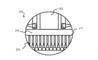
[0027]図2Aは、処理チャンバの中に区切られたプラズマ生成領域を有する例示的なプロセスチャンバシステム200の断面図を示している。膜(例えば、窒化チタン、窒化タンタル、タングステン、シリコン、ポリシリコン、酸化ケイ素、窒化ケイ素、酸窒化ケイ素、酸炭化ケイ素等)のエッチング中に、プロセスガスが、ガス注入アセンブリ205を通って第1プラズマ領域215に流入しうる。遠隔プラズマシステム(RPS)201が、オプションでシステムに含まれてよく、第1ガスを処理しうる。次いで第1ガスは、ガス注入アセンブリ205を通って移動する。注入アセンブリ205は、2つ以上の別個のガス供給チャネルを含んでよく、第2チャネル(図示せず)が含まれている場合には、第2チャネルはRPS201を迂回しうる。 [0027] FIG. 2A shows a cross-sectional view of an exemplary
[0028]冷却プレート203、面板217、イオンサプレッサ223、シャワーヘッド225、及び、基板255が上に配置される基板支持ペデスタル265が図示されており、これらは各々、実施形態に従って含まれうる。ペデスタル265は、基板の温度を制御するために熱交換流体が流通する熱交換チャネルを有しうる。この熱交換チャネルは、処理工程において基板又はウエハを加熱及び/又は冷却するよう動作しうる。ペデスタル265のウエハ支持プラッタは、アルミニウム、セラミック、又はそれらの組み合わせを含んでよく、更に、埋め込み型抵抗加熱素子を使用して、相対的に高い温度(例えば約100℃以下〜約1100°C以上)に到達するように抵抗加熱されうる。 [0028] Cooling
[0029]面板217は、上部が狭く、底部に向かって広がっている、ピラミッド形の、円錐形の、又は別の類似した構造のものでありうる。加えて、面板217は、図示しているように平坦であってもよく、プロセスガスを分散させるために使用される複数の貫通チャネルを含みうる。プラズマ生成ガス及び/又はプラズマ励起種は、RPS201の使用に応じて、第1プラズマ領域215内により均一に送られるよう、図2Bに示している面板217の複数の孔を通過しうる。 [0029]
[0030]例示的な構成は、ガス注入アセンブリ205を、面板217によって第1プラズマ領域215から区切られたガス供給領域258に通じているようにすることを含んでよく、これにより、上記のガス/種が、面板217の孔を通って第1プラズマ領域215に流入する。構造的及び動作的な特徴は、第1プラズマ領域215から供給領域258、ガス注入アセンブリ205、及び流体供給システム210に戻る、プラズマの大量逆流を防止するよう選択されうる。面板217(又はチャンバの上部導電性部分)及びシャワーヘッド225は、これらのフィーチャも間に絶縁リング220が配置された状態で図示されている。これにより、シャワーヘッド225及び/又はイオンサプレッサ223に対して面板217にAC電位が印加されることが可能になる。絶縁リング220は、面板217とシャワーヘッド225及び/又はイオンサプレッサ223との間に配置されてよく、第1プラズマ領域内での容量結合プラズマ(CCP)の形成を可能にする。加えて、バッフル(図示せず)が、第1プラズマ領域215内に配置されうるか、さもなければ、ガス注入アセンブリ205を通ってこの領域に流入する流体の流れに影響を与えるよう、ガス注入アセンブリ205に連結されうる。 [0030] An exemplary configuration may include allowing the
[0031]イオンサプレッサ223は、その構造の全体を通じて複数の開孔を画定するプレート又は他の形状寸法を含んでよく、この構造は、第1プラズマ領域215から出るイオン帯電種の移動を抑制すると共に、非荷電中性種又はラジカル種が、イオンサプレッサ223を通過してサプレッサとシャワーヘッドとの間の活性ガス送達領域に入ることを可能にするよう、構成されている。実施形態では、イオンサプレッサ223は、多種多様な開孔構成を有する有孔プレートを含みうる。上記の非荷電種は、開孔を通じて低反応性キャリアガスと共に搬送される、高反応性種を含みうる。上述したように、孔を通るイオン種の移動は、低減されること、場合によっては完全に抑制されることが可能である。イオンサプレッサ223を通過するイオン種の量を制御することにより、有利には、下にあるウエハ基板と接触することになる混合ガスに対する制御を向上させることが可能であり、ひいては、混合ガスの堆積特性及び/又はエッチング特性の制御も向上させうる。例えば、混合ガスのイオン濃度を調節することで、混合ガスのエッチング選択性(例えばSiNx:SiOxのエッチング比、Si:SiOxのエッチング比など)を大幅に変えることが可能である。堆積が実施される代替的な実施形態では、誘電材料の共形型堆積と流動可能型堆積とのバランスを変化させることも可能である。 [0031] The
[0032]イオンサプレッサ223の複数の開孔は、イオンサプレッサ223を通る活性ガス(すなわちイオン種、ラジカル種、及び/又は中性種)の通過を制御するよう構成されうる。例えば、孔のアスペクト比(すなわち孔の直径対長さの比)及び/又は孔の形状寸法は、イオンサプレッサ223を通過する活性ガス中のイオン帯電種の流れを減少させるように制御されうる。イオンサプレッサ223の孔は、プラズマ励起領域215に面しているテーパ部と、シャワーヘッド225に面している円筒部とを含みうる。円筒部は、シャワーヘッド225を通るイオン種の流れを制御するよう、成形され、寸法設定されうる。サプレッサを通るイオン種の流れを制御する追加手段として、イオンサプレッサ223に調節可能な電気的バイアスが印加されることもある。 [0032] The plurality of apertures in the
[0033]イオンサプレッサ223は、プラズマ生成領域から基板まで移動するイオン帯電種の量を減少させるか、又はかかるイオン帯電種をなくすよう、機能しうる。それでも、非荷電中性種及びラジカル種は、イオンサプレッサの開口を通過して基板と反応しうる。実施形態では、基板を取り囲んでいる反応領域におけるイオン帯電種の完全な除去は実施されない可能性があることに、留意すべきである。ある場合には、エッチングプロセス及び/又は堆積プロセスを実施するために、イオン種は基板に到達することが意図されている。このような場合、イオンサプレッサは、プロセスに役立つレベルで反応領域内のイオン種の濃度を制御するための一助となりうる。 [0033] The
[0034]シャワーヘッド225は、イオンサプレッサ223と組み合わされて、第1プラズマ領域215内に存在するプラズマが基板処理領域233内のガスを直接励起しないことを可能しつつも、励起種がチャンバプラズマ領域215から基板処理領域233内へと移動することを可能しうる。この方式では、チャンバは、エッチング中の基板255にプラズマが接触することを防止するよう、構成されうる。これにより、有利には、基板上にパターニングされた多種多様で複雑な構造体及び膜が保護されうる。かかる複雑な構造体及び膜は、生成されたプラズマが直接接触すると、損傷され、位置ずれし、さもなければ歪みうる。加えて、プラズマが基板に接触すること又は基板平面に接近することが可能である場合、酸化物種がエッチングを行う速度が上昇しうる。したがって、材料の露出した領域が酸化物である場合、基板から離れたところにプラズマを維持することで、この材料は更に保護されうる。 [0034] The
[0035]処理システムは、面板217、イオンサプレッサ223、シャワーヘッド225、及び/又はペデスタル265に電力を提供して、第1プラズマ領域215又は処理領域233内にプラズマを生成するよう、処理チャンバ内に電気的に接続された、電力供給源240を更に含みうる。この電力供給源は、実施されるプロセスに応じてチャンバに調節可能な量の電力を送るよう、構成されうる。かかる構成により、実施中のプロセスにおいて調整可能な(tunable)プラズマが使用されることが可能になりうる。オンオフ機能が与えられていることが多い遠隔プラズマユニットとは異なり、調整可能なプラズマは、特定の量の電力をプラズマ領域215に送るよう構成されうる。これにより、ひいては、前駆体によって作り出されるエッチングプロファイルを強化するためにこれらの前駆体が特定の方式で分離されうるような、特定のプラズマ特性の開発が可能になりうる。 [0035] The processing system provides power to the
[0036]プラズマは、シャワーヘッド225の上方のチャンバプラズマ領域215と、シャワーヘッド225の下方の基板処理領域233のいずれかにおいて、点火されうる。プラズマは、チャンバプラズマ領域215内に、そこに流入したフッ素含有前駆体や他の前駆体などからラジカル前駆体を発生させるために存在しうる。堆積中にチャンバプラズマ領域215内でプラズマを点火するためには、典型的には高周波(RF)範囲内の交流電圧が、処理チャンバの上部導電性部分(面板217など)と、シャワーヘッド225及び/又はイオンサプレッサ223との間に印加されうる。RF電力供給源は、13.56MHzの高RF周波数を発生させうるが、単独で又は13.56MHzの周波数と組み合わされて、別の周波数も発生させうる。 [0036] Plasma can be ignited in either the
[0037]図2Bは、面板217を通る処理ガスの分散に影響を与えるフィーチャの詳細図253である。図2A及び図2Bに示しているように、面板217、冷却プレート203、及びガス注入アセンブリ205は、ガス供給領域258を画定するよう、互いに組み合わされている。ガス供給領域258には、ガス注入アセンブリ205からプロセスガスが送られうる。ガスは、ガス供給領域258に充満し、面板217の開孔259を通って第1プラズマ領域215に流れうる。開孔259は、流れを実質的に一方向へ導くよう構成されうる。これにより、プロセスガスは、処理領域233に流入しうるが、面板217を横断した後にガス供給領域258内に逆流することは部分的又は全面的に防止されうる。 [0037] FIG. 2B is a
[0038]処理チャンバセクション200で使用されるシャワーヘッド225などのガス分散アセンブリは、デュアルチャネルシャワーヘッド(DCSH)と称されてよく、図3に記載の実施形態において更に詳述される。デュアルチャネルシャワーヘッドは、処理領域内に送られる前のエッチング剤とチャンバ構成要素との相互作用、及びエッチング剤同士の相互作用を制限するために、処理領域233の外部でエッチング剤が分離されることを可能にする、エッチングプロセスを提供しうる。 [0038] A gas distribution assembly such as the
[0039]シャワーヘッド225は、上側プレート214と下側プレート216とを備えうる。プレート同士は、プレート間の空間218を画定するよう、互いに連結されうる。プレートは、上側プレート及び下側プレートを通る第1流体チャネル219、及び下側プレート216を通る第2流体チャネル221が設けられるように、連結されうる。形成されたチャネルは、空間218から下側プレート216を通る、第2流体チャネル221だけを介する流体アクセスを提供するよう構成されてよく、第1流体チャネル219は、プレートと第2流体チャネル221との間の空間218から流体的に隔離されうる。空間218は、ガス分散アセンブリ225の一方の側を通じて、流体アクセス可能でありうる。 [0039] The
[0040]図3は、実施形態による、処理チャンバで使用されるシャワーヘッド325の底面図である。シャワーヘッド325は、図2Aに示しているシャワーヘッド225に対応しうる。第1流体チャネル219を図示している貫通孔365は、シャワーヘッド225を通る前駆体の流れを制御し、それに影響を与えるように、複数の形状及び構成を有しうる。第2流体チャネル221を図示している小孔375は、シャワーヘッドの表面上に(貫通孔365の間であっても)実質的に均等に分布してよく、前駆体がシャワーヘッドから出る際の前駆体の混合を他の構成よりも均一にするための一助となりうる。 [0040] FIG. 3 is a bottom view of a
[0041]前述のチャンバは、エッチング方法を含む例示的な方法を実施するのに使用されうる。図4を参照するに、本技術の実施形態による方法400の例示的な工程が示されている。方法の第1工程に先立って、基板は、方法400が実施されうるチャンバの処理領域の中に配置される前に一又は複数の方式で処理されうる。例えば、基板上にIPD層が形成されてよく、次いで、一又は複数のメモリホール又はトレンチが、積み重なった層を通るように形成されうる。IPD層は、任意の数の材料を含んでよく、プレースホルダ材料と誘電体材料とが交互になった層を含みうる。実施形態では、誘電体材料は、酸化ケイ素でありうるか又は酸化ケイ素を含んでよく、プレースホルダ材料は、窒化ケイ素でありうるか又は窒化ケイ素を含みうる。以下の開示では窒化ケイ素及び酸化ケイ素について記述するが、上記の2つの層に使用されることが既知の他の任意の材料が、これらの層のうちの一又は複数を代替しうる。これらの工程の一部又は全部が、前述のように複数のチャンバ若しくはシステムツール内で実施されうるか、又は、方法400の工程が実施されるチャンバを含みうる1つのシステムツールの別々のチャンバ内で実施されうる。 [0041] The chambers described above can be used to perform exemplary methods, including etching methods. With reference to FIG. 4, illustrated are exemplary steps of a
[0042]方法400は、工程405において、半導体処理チャンバの遠隔プラズマ領域に、フッ素含有前駆体及び酸素含有前駆体を流入させることを含みうる。例示的なチャンバは前述したチャンバ200であってよく、チャンバ200は、RPSユニット201と第1プラズマ領域215の一方又は両方を含みうる。これらの領域のいずれか又は両方が、工程405で使用される遠隔プラズマ領域になりうる。工程410において、プラズマが遠隔プラズマ領域内で生成されてよく、このプラズマは、フッ素含有前駆体及び酸素含有前駆体のプラズマ放出物を生成しうる。工程415において、プラズマ放出物がチャンバの処理領域へと流れうる。プラズマ放出物は処理領域内の基板と相互作用してよく、この基板は、積み重なった材料層を通るように形成されたトレンチを含みうる。積み重なった材料層は、例えば窒化ケイ素と酸化ケイ素とが交互になった層を含みうる(ただし、他のプレースホルダ材料及び/又は誘電体材料も使用されうる)。工程420において、前駆体が窒化ケイ素の層を横方向にエッチングしうる。この横方向エッチングは、トレンチ(メモリホールなど)全体で実施されてよく、トレンチ内の側壁から、窒化ケイ素の各層の露出した部分に沿って行われうる。一部の実施形態では、横方向エッチングは、窒化ケイ素層に選択的に実施されてよく、酸化ケイ素又は他の誘電体材料の介在層は実質的に維持されうる。方法400は、横方向エッチング工程が終了するまでの例示的ないくつかの工程において、窒化ケイ素を、トレンチの側壁から10nm未満だけ、横方向にエッチングしうる。 [0042] The
[0043]方法400は、より全体的な拡散が行われることを可能にするためにエッチング速度を低下させること、より全体的な拡散が行われることを可能にするために吸着/脱着速度を低下させることを伴ってよく、又は、ある種のバリアであって、それを通ってエッチング剤が、トレンチ全体へのより全体的な拡散が行われることを可能にする速度で拡散しうる、バリアを伴いうる。例えば、方法400は、窒化ケイ素のエッチングされるべき部分を酸化させることを含みうる。誘電体層は酸化ケイ素でありうるか又は酸化ケイ素を含みうるので、酸化は、窒化ケイ素層のトレンチ全体に露出している(例えばトレンチ側壁を形成している)領域に、優先的又は独占的に行われうる。酸化は、フッ素の又はその他のエッチング剤成分を含んでよく、かかるエッチング剤成分は、酸化した部分を通って拡散して、窒化ケイ素層をエッチングしうる。形成された窒化ケイ素のフッ素化酸化物領域により、トレンチ又はメモリホールの側壁から約10nm以下の、窒化ケイ素の制御された除去が可能になりうる。 [0043] The
[0044]この方法において使用される前駆体は、フッ素含有前駆体だけでなく酸素含有前駆体も含みうる。例示的なフッ素含有前駆体は、三フッ化窒素(NF3)であってよく、これが遠隔プラズマ領域に流入しうる。遠隔プラズマ領域は、処理領域から分離されているが、処理領域に流体的に連結されうる。その他のフッ素源も、三フッ化窒素と併用されうるか、又は三フッ化窒素の代替物として使用されうる。通常、フッ素含有前駆体は、遠隔プラズマ領域に流入してよく、かつ、原子状フッ素、二原子フッ素、三フッ化窒素、四フッ化炭素、フッ化水素、二フッ化キセノン、及び、半導体処理に使用されるか又は役立つ他の様々なフッ素含有前駆体、という群から選択された、少なくとも1つの前駆体を含みうる。酸素含有前駆体は、多種多様な流体を含んでよく、原子状酸素、分子状酸素、N2O、NO、NO2、オゾン、又は、半導体処理に使用されうるか又は役立ちうる他の酸素含有前駆体、のうちの一又は複数を含みうる。前駆体は任意の数のキャリアガスも含んでよく、キャリアガスは、窒素、ヘリウム、アルゴン、又は、他のノーブルな、不活性の、若しくは役に立つ前駆体を含みうる。キャリアガスは前駆体を希釈するために使用されてよく、これにより、エッチング速度が更に低下して、トレンチ全体への十分な拡散が可能になりうる。[0044] The precursors used in this method can include not only fluorine-containing precursors but also oxygen-containing precursors. An exemplary fluorine-containing precursor may be nitrogen trifluoride (NF3 ), which can flow into the remote plasma region. The remote plasma region is separate from the processing region, but can be fluidly coupled to the processing region. Other fluorine sources can be used in combination with nitrogen trifluoride or can be used as an alternative to nitrogen trifluoride. Typically, the fluorine-containing precursor may flow into the remote plasma region and is atomic fluorine, diatomic fluorine, nitrogen trifluoride, carbon tetrafluoride, hydrogen fluoride, xenon difluoride, and semiconductor processing May include at least one precursor selected from the group of various other fluorine-containing precursors used or useful. Oxygen-containing precursors may include a wide variety of fluids, including atomic oxygen, molecular oxygen, N2 O, NO, NO2 , ozone, or other oxygen-containing precursors that may be used or useful in semiconductor processing. One or more of the bodies may be included. The precursor may include any number of carrier gases, and the carrier gas may include nitrogen, helium, argon, or other noble, inert, or useful precursor. The carrier gas may be used to dilute the precursor, which can further reduce the etch rate and allow sufficient diffusion throughout the trench.
[0045]方法400は、実施形態では、前駆体の酸素とフッ素との比率を調整することを伴いうる。例えば、酸素前駆体とフッ素前駆体との比率は、実施形態では、約20:1以上の流量比を含みうる。酸素流量を増大させ、フッ素の含有を制限することにより、エッチングの開始に先立って窒化ケイ素の露出した領域に酸化が行われうる。したがって、酸化層は、バリア層(それを通ってフッ素含有エッチング剤が拡散しうる)と同様に作用しうる。窒化ケイ素の酸化部分を通って拡散する時間は、前駆体をメモリホール又はトレンチの底まで拡散させる時間よりも長くなりうる。この方式では、窒化ケイ素の露出した領域をエッチングする前に、この領域の各々に沿って酸化層が形成されうる。次いで、エッチング剤がトレンチ及び酸化領域の全体に均一に分散され、窒化ケイ素の露出した各領域に実質的に同等量のエッチングを行うことが可能になりうる。同様に、混合物中のフッ素の量を制限することによって、窒化ケイ素の露出した各領域からエッチングされる材料の量が制御されうる。 [0045] The
[0046]方法400などの例示的な方法では、酸素含有前駆体とフッ素含有前駆体との比率は、除去されるべき窒化ケイ素の厚さに関連しうる。例えば、より多くの窒化ケイ素を除去しうる方法では、前駆体中に更なるフッ素含有前駆体が含まれうるか、又は、動作時間が延長されうる。トレンチ内の酸化ケイ素の露出した各領域に約10nm未満の横方向エッチングを行うためには、酸素含有前駆体とフッ素含有前駆体との比率は、約25:1以上でありうるか、又は、約30:1以上、約35:1以上、約40:1以上、約45:1以上、約50:1以上、約55:1以上、約60:1以上、約65:1以上、約70:1以上、約75:1以上、約80:1以上、若しくはそれ以上、並びに、上述の範囲のいずれかの中に含まれる任意のより細かな範囲でありうる。例えば、約60:1以上の流量により、窒化ケイ素の露出した各領域にフッ素化酸化物領域を形成することが可能になりうる。流量比は、実施形態では、トレンチの長さ全体にわたってエッチングされる窒化ケイ素の量を低減するために、40:1を上回るように維持されうる。混合物中のフッ素の量が増加されると、酸化部分が形成される前に、トレンチの上部又はその付近の窒化ケイ素の領域でエッチングが開始されうる。このような場合でも、トレンチ内には、トレンチの上部から底部に至る窒化ケイ素層のV型プロファイルなどのプロファイルが作り出されうる。 [0046] In an exemplary method, such as
[0047]横方向エッチングが実施されうるトレンチ又はメモリホールのアスペクト比は高いことから、従来型の乾式技術では、V型プロファイルが不可避なこともある。例示的なトレンチの直径又は幅は数ナノメートル〜数十ナノメートル以下でありうる一方で、このトレンチの高さはおよそ数ミクロン以上でありうる。これにより、20:1を上回る、50:1を上回る、75:1を上回る、100:1を上回る、又はそれを超えることもある、アスペクト比(又は高さと幅との比率)が生じうる。したがって、実施形態では、各トレンチ内で、25層を超える、50層を超える、75層を超える、又は100層を超える、交互になったプレースホルダ材料と誘電体材料とが形成され、処理されうる。 [0047] Due to the high aspect ratio of trenches or memory holes where lateral etching can be performed, V-type profiles may be unavoidable with conventional dry technology. While the diameter or width of an exemplary trench can be a few nanometers to tens of nanometers or less, the height of the trench can be approximately a few microns or more. This can result in an aspect ratio (or ratio of height to width) that is greater than 20: 1, greater than 50: 1, greater than 75: 1, greater than 100: 1, or even greater. Thus, in embodiments, in each trench, more than 25 layers, more than 50 layers, more than 75 layers, or more than 100 layers, alternating placeholder and dielectric materials are formed and processed. sell.
[0048]乾式エッチング剤又はガス状エッチング剤が移動しうる距離が長いことから、エッチング剤がトレンチの底部に到達していなくとも、トレンチの上部領域は大量のエッチング剤に暴露されることがある。この方式では、トレンチの上方領域にある窒化ケイ素は、トレンチの底の部分よりも多くエッチングされうる。湿式エッチング技法は、より均一に窒化ケイ素の層をエッチングしうるが、エッチング剤の特性及び滞留時間により、10ナノメートル前後だけエッチングすることは不可能でありうる。したがって、本技術とは異なり、各窒化ケイ素層から一定量の材料(例えば数ナノメートルのみ)を微細にエッチングすることが可能でありうると共に、エッチングされる窒化ケイ素のプロファイルが平坦に、又はトレンチ全体を通じて実質的に同じようになりうる、従来型の技術はない。しかし本技術は、より均一なエッチングプロセスが行われることを可能にするために、記載されている方式のうちの任意のものでエッチング剤を制限することによって、拡散経路の拡張を相殺しうる。 [0048] Due to the long distance traveled by dry or gaseous etchants, the upper region of the trench may be exposed to a large amount of etchant even if the etchant does not reach the bottom of the trench. . In this manner, the silicon nitride in the upper region of the trench can be etched more than the bottom portion of the trench. Wet etching techniques can more uniformly etch a layer of silicon nitride, but due to the properties of the etchant and the residence time, it may not be possible to etch only around 10 nanometers. Thus, unlike the present technology, it may be possible to finely etch a certain amount of material (eg only a few nanometers) from each silicon nitride layer and the etched silicon nitride profile is flat or trenched There is no conventional technique that can be substantially the same throughout. However, the technique can offset the diffusion path expansion by limiting the etchant in any of the manners described to allow a more uniform etching process to be performed.
[0049]プロセス条件も、本技術による方法400並びに他のエッチング方法において実施される工程に影響を与えうる。方法400の各工程は、実施形態では、一定の温度において実施されうるが、一部の実施形態では、種々の工程中に温度が調節されうる。例えば、横方向エッチング工程420における基板、ペデスタル、又はチャンバの温度は、実施形態において、約−100°C〜約100°Cに維持されうる。温度は更に、約80°C以下、約60°C以下、約40°C以下、約20°C以下、約0°C以下、約−20°C以下、約−40°C以下、又はこれらを下回るように、維持されうる。温度はエッチングプロセス自体に影響を与えることがあり、高温は、エッチング速度を上昇させうるか、エッチングを増大させうるか、又は、他の影響をもたらしうる。同様に、低温により、エッチング動作は鈍化することがあり、エッチングの前に又は最低限度のエッチングしか行われていないうちに窒化ケイ素を部分的に酸化させることが、可能になりうる。ゆえに、一部の実施形態では、温度を約0°C以下に維持することで、トレンチの上部とトレンチの底部における窒化ケイ素のエッチング量がより均一になりうる。温度が上昇するにつれて、エッチング動作が更に誘電体領域に影響を与え始めることがあり、誘電体材料(酸化ケイ素など)の露出した角部又は領域が若干丸くなりうる。 [0049] Process conditions may also affect the steps performed in
[0050]チャンバ内の圧力も実施される工程に影響を与えることがあり、実施形態では、チャンバ圧力は、約10Torr未満、約5Torr未満、又は約1Torr未満に維持されうる。実施形態では、約1Torr以下の圧力により、前駆体又はプラズマ放出物がより容易にトレンチ又はメモリホールに流入することが可能になりうる。しかし、圧力が約0.5Torr未満に低減されると、遠隔プラズマは、影響を受けることがあり、安定性が低下しうるか、又は不安定になりうる。前述したように、遠隔プラズマは、RPSユニットを含んでよく、ウエハ平面のプラズマを制限するか又はなくすためにチャンバの処理領域から物理的に区切られた、チャンバの領域又は部分であることもある。RPSユニットが利用される一部の実施形態では、プラズマを安定させるためにRPSユニット内の高圧を維持すると共に、トレンチ内の前駆体又はプラズマ放出物の流れを改善するようチャンバ内の低圧を維持するために、チョークが利用されうる。したがって、チャンバ内でターボ分子ポンプが利用され、チャンバ圧力を数ミリTorrまで引き下げることが可能になる一方で、RPSは約0.6Torr以上に維持される。 [0050] Pressure in the chamber may also affect the process being performed, and in embodiments, the chamber pressure may be maintained at less than about 10 Torr, less than about 5 Torr, or less than about 1 Torr. In embodiments, a pressure of about 1 Torr or less may allow precursors or plasma emissions to flow more easily into the trench or memory hole. However, when the pressure is reduced below about 0.5 Torr, the remote plasma may be affected and may become less stable or unstable. As described above, the remote plasma may include an RPS unit and may be a region or portion of the chamber that is physically separated from the processing region of the chamber to limit or eliminate the wafer plane plasma. . In some embodiments where an RPS unit is utilized, the high pressure in the RPS unit is maintained to stabilize the plasma and the low pressure in the chamber is maintained to improve the flow of precursor or plasma emissions in the trench. A choke can be used to do this. Thus, a turbomolecular pump is utilized in the chamber, allowing the chamber pressure to be reduced to a few milliTorr while maintaining the RPS above about 0.6 Torr.
[0051]チャンバ条件、流量比、及びその他の動作特性は、窒化ケイ素領域の制御されたエッチングを実施するよう、調節されうる。例えば、窒化ケイ素の各領域は、トレンチ側壁から、約10nm以下の距離又は深さまで横方向にエッチングされうる。加えて、本技術により、窒化ケイ素が、堆積されるべき材料の厚さに応じて、約9nm以下、約8nm以下、約7nm以下、約6nm以下、約5nm以下、約4nm以下、約3nm以下、約2nm以下、約1nm以下、又はこれらを下回る距離又は深さまで、横方向にエッチングされることが可能になりうる。実施形態では、窒化ケイ素の各層は、トレンチ側壁から、約1nm〜約7nm、又は約2nm〜約6nmの深さ又は距離まで、エッチングされうる。 [0051] Chamber conditions, flow ratios, and other operating characteristics can be adjusted to perform a controlled etch of the silicon nitride region. For example, each region of silicon nitride can be etched laterally from a trench sidewall to a distance or depth of about 10 nm or less. In addition, the present technology allows silicon nitride to be about 9 nm or less, about 8 nm or less, about 7 nm or less, about 6 nm or less, about 5 nm or less, about 4 nm or less, about 3 nm or less, depending on the thickness of the material to be deposited. , About 2 nm or less, about 1 nm or less, or a distance or depth below them can be allowed to be etched laterally. In embodiments, each layer of silicon nitride can be etched from the trench sidewalls to a depth or distance of about 1 nm to about 7 nm, or about 2 nm to about 6 nm.
[0052]本技術による工程を実施することによって、エッチング能力(power)は、エッチング物質の拡散能力に関連して低下しうる。これにより、トレンチ又はメモリホール内に露出した各窒化ケイ素領域に、より均一であるか、実質的に均一であるか、又は本質的に(essentially)均一である、エッチングを実施することが可能になりうる。実施形態では、トレンチ又はメモリホールの上部又はその付近(例えば、上部から2層以内、4層以内、6層以内、8層以内、10層以内、又はそれを上回る数の層以内)の窒化ケイ素領域において、側壁から測定して、トレンチ又はメモリホールの底部又はその付近(例えば、底部から2層以内、4層以内、6層以内、8層以内、10層以内、又はそれを上回る数の層以内)の窒化ケイ素の層又は領域と同様の量の材料が、エッチングされうる。 [0052] By performing a process according to the present technology, the etch power may be reduced in relation to the ability of the etchant to diffuse. This allows each silicon nitride region exposed in the trench or memory hole to be etched more uniformly, substantially uniform, or essentially uniform. Can be. In embodiments, silicon nitride at or near the top of a trench or memory hole (eg, within 2 layers, 4 layers, 6 layers, 8 layers, 10 layers, or more layers from the top). In the region, the number of layers measured from the side wall or near the bottom of the trench or memory hole (for example, within 2 layers, within 4 layers, within 6 layers, within 8 layers, within 10 layers, or more from the bottom) A similar amount of material can be etched.
[0053]比較されている2つの層は、構造体における積み重なった層(これらを通ってトレンチ又はメモリホールがエッチングされている)の総数に応じて、少なくとも1層、少なくとも5層、少なくとも11層、少なくとも21層、少なくとも51層又はそれを上回る数の層によって、分離されうる。比較されている2つの層の横方向エッチングは、上方の層が下方の層よりも30%以下しか多くエッチングされないという意味において、約30%以下しか相違しないことがある。加えて、本技術により2つの層の横方向エッチングが実施されれば、この2つの層の間のエッチングされる窒化ケイ素の量の差異は、約25%以下、約20%以下、約15%以下、約10%以下、約5%以下、約1%以下、又はゼロになり、差異がゼロになる場合には、酸化ケイ素の両方の領域は、トレンチの側壁から等しい深さ又は距離までエッチングされる。 [0053] The two layers being compared are at least one layer, at least five layers, at least eleven layers, depending on the total number of stacked layers in the structure through which the trench or memory hole has been etched. Can be separated by at least 21 layers, at least 51 layers or more. The lateral etching of the two layers being compared may differ by no more than about 30% in the sense that the upper layer is etched no more than 30% more than the lower layer. In addition, if two layers are laterally etched according to the present technique, the difference in the amount of silicon nitride etched between the two layers is less than about 25%, less than about 20%, about 15% Below, about 10% or less, about 5% or less, about 1% or less, or zero, and if the difference is zero, both regions of silicon oxide are etched to an equal depth or distance from the sidewalls of the trench. Is done.
[0054]上記のように、横方向エッチングは、窒化ケイ素層のトレンチに隣接した部分を酸化させることを含んでよく、フッ素化酸化物を形成することを伴いうる。フッ素化酸化物中の又はフッ素化酸化物の近位のフッ素は、窒化ケイ素又は窒化ケイ素の酸化した部分を横方向にエッチングする工程において、層又は酸化した部分を通って拡散しうる。一部の実施形態では、方法はこの段階で終了しうる。例えば、このプロセスにより、酸化した窒化ケイ素のトレンチに隣接した領域は、例えば約1nm、約2nm、又はそれよりも多く、部分的に除去されうる。したがって、酸化が窒化ケイ素内にもっと深く浸透していても、材料は単なるプレースホルダであり、その後に除去されうるので、後続の工程は実施されうる。しかし、一部の実施形態では、方法は、窒化ケイ素からフッ素化酸化物を除去することを更に含みうる。これらの工程は、以下で図5を参照して解説するが、例えばフッ素含有前駆体及び水素含有前駆体から発生したプラズマ放出物を用いて、フッ素化酸化物をエッチングすることを含みうる。 [0054] As noted above, lateral etching may include oxidizing portions of the silicon nitride layer adjacent to the trenches and may involve forming a fluorinated oxide. Fluorine in or near the fluorinated oxide can diffuse through the layer or oxidized portion in the lateral etching of silicon nitride or oxidized portions of silicon nitride. In some embodiments, the method may end at this stage. For example, with this process, the region adjacent to the oxidized silicon nitride trench can be partially removed, for example, about 1 nm, about 2 nm, or more. Thus, even if the oxidation penetrates deeper into the silicon nitride, the material is merely a placeholder and can be removed thereafter so that subsequent steps can be performed. However, in some embodiments, the method can further include removing the fluorinated oxide from the silicon nitride. These steps, described below with reference to FIG. 5, may include etching the fluorinated oxide using, for example, plasma emissions generated from a fluorine-containing precursor and a hydrogen-containing precursor.
[0055]図5は、本技術の実施形態による、方法500の例示的な工程を示している。方法500は、上述した方法400の工程の一部又は全部、及び、そこで述べた構成要素又は条件のうち任意のものを含みうる。方法500は、例えば、半導体処理チャンバの遠隔プラズマ領域に、フッ素含有前駆体及び酸素含有前駆体を流入させることを含みうる。一部の実施形態では、前駆体のうちの一又は複数が遠隔プラズマ領域に流入しうる一方で、一又は複数の別の前駆体は、遠隔プラズマ領域を迂回してよく、後続のプラズマ処理においてプラズマ放出物と接触しうる。遠隔プラズマ領域は、処理チャンバの仕切られた領域、又は処理チャンバに流体的に連結された遠隔セクションを含む、一又は複数の遠隔プラズマ領域を含みうる。したがって、一部の前駆体は、他のラジカル成分との接触によってのみ励起されうる他の実施形態では、全ての前駆体が遠隔プラズマ領域を通って流れうる。 [0055] FIG. 5 illustrates example steps of a
[0056]工程505において、プラズマは、一次前駆体でありうる上記の前駆体で形成されうる。プラズマは、フッ素含有前駆体及び酸素含有前駆体の一次プラズマ放出物を生成しうる。一次プラズマ放出物は、基板が収納されている処理チャンバの処理領域に流入しうる。基板は、前述したような、窒化ケイ素と酸化ケイ素とが交互になった層を含む積み重なった層を通るように形成された、トレンチ(メモリホールなど)を含みうる。工程510において、窒化ケイ素の各層にフッ素化酸化物領域を作り出すために、窒化ケイ素のトレンチ側壁から延在している部分が、一次プラズマ放出物によって酸化されうる。 [0056] In
[0057]その後、酸化工程が実施されたのと同じチャンバ内で、更なる工程が実施されうる。例えば、方法500は、工程515において、二次プラズマ放出物を発生させるために、半導体処理チャンバの遠隔プラズマ領域にフッ素含有前駆体を流入させつつプラズマを生成することを、更に含みうる。工程515は、水素含有前駆体などの更なる前駆体を含みうる。水素含有前駆体は、水素、炭化水素、水、過酸化水素、又は、当業者であれば理解しうる、水素を含みうるその他の物質を、含みうる。二次前駆体には、キャリアガスや不活性物質といった更なる前駆体も含まれうる。前駆体のうちの一又は複数は二次プラズマ放出物を発生させるために使用されてよく、実施形態では、これらの前駆体の一部又は全部が、二次プラズマ放出物を発生させるために遠隔プラズマ領域に存在しうる。加えて、前駆体のうちの一又は複数は、遠隔プラズマ領域を迂回してよく、処理チャンバの更なる領域に流入しうる。上記の前駆体は、処理領域又はチャンバの別のどこかの領域において、プラズマ放出物と混合されうる。 [0057] Further steps may then be performed in the same chamber in which the oxidation step was performed. For example, the
[0058]二次プラズマ放出物は、生成されると、半導体処理チャンバの処理領域に流入してよく、そこで、基板と接触し、トレンチ内に拡散しうる。工程520において、酸化した窒化ケイ素又はフッ素酸化物領域が、窒化ケイ素の各層から横方向にエッチングされうる。したがって、窒化ケイ素は、約1nm〜約8nm、又は前述した他の範囲のいずれかの深さまで、酸化されうる。加えて、工程510では、窒化ケイ素層は、例えば前記の任意の深さ又は距離まで、トレンチ側壁から部分的にエッチングされうるが、窒化ケイ素層の酸化した部分は、この工程の後にも維持されうる。この酸化した領域は、例えば構造体のセル領域を分離させうる酸化ケイ素の誘電体層よりも、品質が低い酸化物でありうる。したがって、横方向エッチング工程520は、高品質の酸化ケイ素よりも低品質の酸化ケイ素を選択するプロセスを伴いうる。 [0058] As secondary plasma emissions are generated, they may flow into the processing region of the semiconductor processing chamber where they may contact the substrate and diffuse into the trenches. In
[0059]上述したように、この工程により、酸化ケイ素の層に、トレンチの上部から底部まで実質的に均一な、上部−底部ローディングとも称されるエッチングが行われうる。これにより、トレンチの上側領域における窒化ケイ素の層と、トレンチの下側領域における窒化ケイ素の層での横方向エッチング量が、約20%未満、又は前述した差異及び/又は深さのいずれかの分しか、相違しないことが可能になりうる。この均一性は、部分的には、工程が実施される条件により生じうる。例えば、一次プラズマ放出物を発生させるために使用される酸素含有前駆体とフッ素含有前駆体との流量比は、約60:1以上でありうる。これにより、酸化層(これを通ってフッ素が拡散しうる)の形成が可能になりうる。このことが、前駆体がトレンチ全体に拡散している間の、窒化ケイ素領域のエッチング速度を鈍化又は低下させうる。加えて、このエッチング方法における半導体処理チャンバの中の温度は、その時点でのエッチング速度を更に低下させるために、約0°C以下にされうる。 [0059] As described above, this step can cause the silicon oxide layer to be etched, also referred to as top-bottom loading, which is substantially uniform from the top to the bottom of the trench. This allows the amount of lateral etching in the silicon nitride layer in the upper region of the trench and the silicon nitride layer in the lower region of the trench to be less than about 20%, or any of the aforementioned differences and / or depths. Only minutes may be possible to make a difference. This uniformity can be caused in part by the conditions under which the process is performed. For example, the flow ratio of oxygen-containing precursor to fluorine-containing precursor used to generate the primary plasma emission can be about 60: 1 or higher. This may allow the formation of an oxide layer (through which fluorine can diffuse). This can slow or reduce the etch rate of the silicon nitride region while the precursor diffuses throughout the trench. In addition, the temperature in the semiconductor processing chamber in this etching method can be reduced to about 0 ° C. or less in order to further reduce the current etch rate.
[0060]図6Aから図6Cを参照するに、本技術の実施形態による、処理中の基板600の概略断面図を示している。図6Aに示しているように、基板605は、基板の上にある複数の積み重なった層であって、シリコン、シリコンゲルマニウム、又は他の基板材料でありうる、複数の積み重なった層を有しうる。これらの層は、層になっている、酸化ケイ素でありうる誘電体材料610と、窒化ケイ素でありうるプレースホルダ材料620とを含む、IPD層を含みうる。プレースホルダ材料620は、後続工程で個々のメモリセルを作り出すために除去されることになっている材料でありうるか、又はかかる材料を含みうる。7つの材料層だけが図示されているが、例示的な構造体は、任意の数の前述した層を含みうる。メモリホールでありうるトレンチ630は、積層構造を通って基板605の平面に達するように画定されうる。トレンチ630は、誘電体材料610とプレースホルダ材料620とが交互になった層で構成されうる、側壁632によって画定されうる。 [0060] Referring to FIGS. 6A-6C, there is shown a schematic cross-sectional view of a
[0061]図6Bでは、本技術による方法が図4から図5に関連して上述したように実施された後の構造体が示されている。窒化ケイ素層620の各露出面の一部分が酸化されて、酸化した領域625が作り出されうる。酸化した領域は、窒化ケイ素の一部分をエッチングするためのフッ素化酸化物でありうる。図示していないが、酸化領域625は、前述したように、トレンチ630の側壁632から、例えば、最大で若しくはおおよそ1nm、2nm、3nm、又はそれを上回る距離まで、又はその距離を越えて、部分的に陥凹化されうる。例えば誘電体層610は既に酸化物でありうるので、これらの層は酸化による影響を受けないことがある。しかし、基板605は酸化薄層627を含んでよく、酸化薄層627は、窒化ケイ素層620の酸化の深さを下回りうるか、又はかかる深さと等しいものでありうる。他の実施形態では、基板は、最低限しか酸化されないか、又は実質的に酸化されないことがある。 [0061] In FIG. 6B, the structure is shown after the method according to the present technique has been performed as described above in connection with FIGS. A portion of each exposed surface of the
[0062]図6Cでは、本技術による更なる方法又は工程が図4から図5に関連して上述したように実施された後の構造体が示されている。窒化ケイ素層620の酸化した部分を除去するために、エッチング工程が実施されうる。エッチングにより酸化した部分が除去されてよく、これにより、窒化ケイ素の、トレンチ630及び酸化ケイ素層610から陥凹化した領域が形成されうる。これらの層は、約10nm未満、約2nm〜約6nm、又は、この開示の他所に記載したいずれかの範囲内で、陥凹化しうる。基板605は、トレンチ630の底部が最低限しかエッチングされず、約5nm以下の量しか減少せず、約3nm以下、約2nm以下、約1nm以下という量しか減少しないことがあるか、又は、窒化ケイ素の横方向エッチング工程において実質的に維持されうる。 [0062] In FIG. 6C, the structure is shown after further methods or steps according to the present technique have been performed as described above in connection with FIGS. An etching process may be performed to remove the oxidized portion of the
[0063]上記の説明には、本技術の様々な実施形態の理解を促すために、解説を目的として多数の詳細事項を明記してきた。しかし、特定の実施形態は、これらの詳細事項の一部がなくとも、又は追加の詳細実行があっても実践されうることが、当業者には自明であろう。 [0063] In the description above, numerous details have been set forth for purposes of explanation in order to facilitate understanding of various embodiments of the technology. However, it will be apparent to one skilled in the art that particular embodiments may be practiced without some of these details or with additional details.
[0064]いくつかの実施形態を開示したが、実施形態の本質から逸脱しなければ、様々な改変例、代替構造、及び均等物が使用されうることは、当業者によって認識されよう。加えて、本技術を不必要に不明瞭にすることを避けるために、いくつかの周知のプロセス及び要素については説明していない。したがって、上記の説明は、本技術の範囲を限定するものと解釈すべきでない。加えて、方法又はプロセスは連続した又は段階的なものとして説明されうるが、これらの工程が同時に又は記載とは異なった順序で実施されうることを、理解されたい。 [0064] Although several embodiments have been disclosed, those skilled in the art will recognize that various modifications, alternative constructions, and equivalents may be used without departing from the essence of the embodiments. In addition, some well-known processes and elements have not been described in order to avoid unnecessarily obscuring the present technology. Accordingly, the above description should not be taken as limiting the scope of the technology. In addition, although a method or process may be described as sequential or stepwise, it should be understood that these steps may be performed simultaneously or in a different order than described.
[0065]値の範囲が提供されている場合、その範囲の上限値と下限値との間の介在値の各々は、(文脈上そうでないと明確に指示されない限り)下限値の最も小さい単位まで具体的に開示されると理解される。記載された範囲における任意の記載値同士又は記載されていない介在値同士の間のより狭い範囲、及び、かかる記載範囲における他の記載値又は介在値は全て、包含される。上記の狭い範囲の上限値及び下限値は、個別に、この範囲に含まれうるか又はこの範囲から除外されうる。この狭い範囲に限界値のいずれかが含まれるか、どちらも含まれないか、又は両方が含まれる場合の各範囲も、記載範囲内に特に除外された限界値があることを条件として、本技術に包含される。記載範囲が限界値の一方又は両方を含む場合、含有された限界値のいずれか又は両方を除外する範囲も、含まれる。 [0065] Where a range of values is provided, each intervening value between the upper and lower limits of the range is to the smallest unit of the lower limit (unless explicitly indicated otherwise in the context). It is understood that it is specifically disclosed. Narrower ranges between any stated values in the stated range or intervening intervening values and all other stated or intervening values in such stated ranges are all included. The upper and lower limits of the narrow range can be individually included in or excluded from this range. Each range in which this narrow range contains either or both of the limit values, or both are included, provided that there is a limit value specifically excluded within the stated range. Included in technology. Where the stated range includes one or both of the limit values, ranges excluding either or both of the included limit values are also included.
[0066]本書及び付随する特許請求の範囲において、単数形の「1つの(a、an)」、及び「前記(the)」は、(文脈上そうでないと明確に指示されない限り)複数形の意味を含む。ゆえに、例えば、「1つの前駆体(a precursor)」への言及は、複数のかかる前駆体を含み、「前記層(the layer)」への言及は、当業者には既知の一又は複数の層及びその均等物への言及を含み、その他も同様である。 [0066] In this document and the appended claims, the singular forms “a”, “an”, and “the” refer to the plural form unless the context clearly dictates otherwise. Includes meaning. Thus, for example, reference to “a precursor” includes a plurality of such precursors, and reference to “the layer” includes one or more known to those skilled in the art. Includes references to layers and their equivalents, and so on.
[0067]また、「備える(comprise(s)/comprising)」、「含有する(contain(s)/containing)」、「含む(include(s)/including)」という語は、この明細書及び以下の特許請求の範囲で使用される場合には、記載された特徴、整数、構成要素、又は工程の存在を特定することを意図しているが、一又は複数の、他の特徴、整数、構成要素、工程、作用、又はグループの存在又は追加を除外するものではない。 [0067] Also, the terms “comprise (s) / comprising”, “contain (s) / containing”, “include (s) / inclusion” are used in this specification and below. Is intended to identify the presence of the described feature, integer, component, or process, but may include one or more other features, integers, configurations It does not exclude the presence or addition of elements, steps, actions or groups.
Claims (15)
Translated fromJapanese前記フッ素含有前駆体及び前記酸素含有前駆体のプラズマ放出物を生成するために、前記遠隔プラズマ領域内でプラズマを形成することと、
前記半導体処理チャンバの処理領域に前記プラズマ放出物を流入させることであって、前記処理領域の中に基板が配置されており、前記基板は、窒化ケイ素と酸化ケイ素とが交互になった層を含む積み重なった層を通るように形成された、トレンチを備える、前記プラズマ放出物を流入させることと、
前記酸化ケイ素の層を実質的に維持しつつ、前記トレンチの側壁から前記窒化ケイ素の層を横方向にエッチングすることであって、前記窒化ケイ素の層は、前記トレンチの前記側壁から10nm未満だけ横方向にエッチングされる、前記窒化ケイ素の層を横方向にエッチングすることとを含む、エッチング方法。Flowing a fluorine-containing precursor and an oxygen-containing precursor into a remote plasma region of a semiconductor processing chamber;
Forming a plasma in the remote plasma region to produce plasma emissions of the fluorine-containing precursor and the oxygen-containing precursor;
Flowing the plasma emission into a processing region of the semiconductor processing chamber, wherein a substrate is disposed in the processing region, the substrate comprising layers of alternating silicon nitride and silicon oxide. Flowing said plasma emission comprising a trench formed to pass through a stacked layer including;
Etching the silicon nitride layer laterally from the sidewalls of the trench while substantially maintaining the silicon oxide layer, wherein the silicon nitride layer is less than 10 nm from the sidewalls of the trench; Etching laterally, etching the silicon nitride layer laterally.
前記フッ素含有前駆体及び前記酸素含有前駆体の一次プラズマ放出物を生成するために、前記遠隔プラズマ領域内でプラズマを形成することと、
前記半導体処理チャンバの処理領域に前記一次プラズマ放出物を流入させることであって、前記処理領域の中に基板が配置されており、前記基板は、窒化ケイ素と酸化ケイ素とが交互になった層を含む積み重なった層を通るように形成された、トレンチを備える、前記一次プラズマ放出物を流入させることと、
窒化ケイ素の各層にフッ素化酸化物領域を作り出すために、前記トレンチの側壁から前記窒化ケイ素の一部分を酸化させることと、
二次プラズマ放出物を発生させるために、前記半導体処理チャンバの前記遠隔プラズマ領域にフッ素含有前駆体を流入させつつプラズマを生成することと、
前記半導体処理チャンバの前記処理領域に前記二次プラズマ放出物を流入させることと、
窒化ケイ素の各層から前記フッ素化酸化物領域を横方向にエッチングすることとを含む、エッチング方法。Flowing a fluorine-containing precursor and an oxygen-containing precursor into a remote plasma region of a semiconductor processing chamber;
Forming a plasma in the remote plasma region to produce a primary plasma emission of the fluorine-containing precursor and the oxygen-containing precursor;
Injecting the primary plasma emission into a processing region of the semiconductor processing chamber, wherein a substrate is disposed in the processing region, the substrate comprising layers of alternating silicon nitride and silicon oxide Flowing said primary plasma emission comprising a trench formed to pass through a stacked layer comprising:
Oxidizing a portion of the silicon nitride from the sidewalls of the trench to create a fluorinated oxide region in each layer of silicon nitride;
Generating a plasma while flowing a fluorine-containing precursor into the remote plasma region of the semiconductor processing chamber to generate secondary plasma emissions;
Flowing the secondary plasma emission into the processing region of the semiconductor processing chamber;
Etching the fluorinated oxide region laterally from each layer of silicon nitride.
Applications Claiming Priority (3)
| Application Number | Priority Date | Filing Date | Title |
|---|---|---|---|
| US15/288,898 | 2016-10-07 | ||
| US15/288,898US10062579B2 (en) | 2016-10-07 | 2016-10-07 | Selective SiN lateral recess |
| PCT/US2017/055431WO2018067881A1 (en) | 2016-10-07 | 2017-10-05 | Selective sin lateral recess |
Publications (1)
| Publication Number | Publication Date |
|---|---|
| JP2019530982Atrue JP2019530982A (en) | 2019-10-24 |
Family
ID=61829044
Family Applications (1)
| Application Number | Title | Priority Date | Filing Date |
|---|---|---|---|
| JP2019518433ACeasedJP2019530982A (en) | 2016-10-07 | 2017-10-05 | Selective lateral depression of SiN |
Country Status (6)
| Country | Link |
|---|---|
| US (2) | US10062579B2 (en) |
| JP (1) | JP2019530982A (en) |
| KR (1) | KR20190053282A (en) |
| CN (1) | CN109906500A (en) |
| TW (1) | TW201826383A (en) |
| WO (1) | WO2018067881A1 (en) |
Cited By (3)
| Publication number | Priority date | Publication date | Assignee | Title |
|---|---|---|---|---|
| JP2020167277A (en)* | 2019-03-29 | 2020-10-08 | アプライド マテリアルズ インコーポレイテッドApplied Materials,Incorporated | Semiconductor processing chamber multi-stage mixing device |
| US11515179B2 (en) | 2018-02-15 | 2022-11-29 | Applied Materials, Inc. | Semiconductor processing chamber multistage mixing apparatus |
| JP2023530554A (en)* | 2021-03-12 | 2023-07-19 | アプライド マテリアルズ インコーポレイテッド | Removal of isotropic silicon nitride |
Families Citing this family (84)
| Publication number | Priority date | Publication date | Assignee | Title |
|---|---|---|---|---|
| US10283321B2 (en) | 2011-01-18 | 2019-05-07 | Applied Materials, Inc. | Semiconductor processing system and methods using capacitively coupled plasma |
| US9132436B2 (en) | 2012-09-21 | 2015-09-15 | Applied Materials, Inc. | Chemical control features in wafer process equipment |
| US10256079B2 (en) | 2013-02-08 | 2019-04-09 | Applied Materials, Inc. | Semiconductor processing systems having multiple plasma configurations |
| US9362130B2 (en) | 2013-03-01 | 2016-06-07 | Applied Materials, Inc. | Enhanced etching processes using remote plasma sources |
| US9309598B2 (en) | 2014-05-28 | 2016-04-12 | Applied Materials, Inc. | Oxide and metal removal |
| US9966240B2 (en) | 2014-10-14 | 2018-05-08 | Applied Materials, Inc. | Systems and methods for internal surface conditioning assessment in plasma processing equipment |
| US9355922B2 (en) | 2014-10-14 | 2016-05-31 | Applied Materials, Inc. | Systems and methods for internal surface conditioning in plasma processing equipment |
| US11637002B2 (en) | 2014-11-26 | 2023-04-25 | Applied Materials, Inc. | Methods and systems to enhance process uniformity |
| US10573496B2 (en) | 2014-12-09 | 2020-02-25 | Applied Materials, Inc. | Direct outlet toroidal plasma source |
| US10224210B2 (en) | 2014-12-09 | 2019-03-05 | Applied Materials, Inc. | Plasma processing system with direct outlet toroidal plasma source |
| US11257693B2 (en) | 2015-01-09 | 2022-02-22 | Applied Materials, Inc. | Methods and systems to improve pedestal temperature control |
| US20160225652A1 (en) | 2015-02-03 | 2016-08-04 | Applied Materials, Inc. | Low temperature chuck for plasma processing systems |
| US9728437B2 (en) | 2015-02-03 | 2017-08-08 | Applied Materials, Inc. | High temperature chuck for plasma processing systems |
| US9741593B2 (en) | 2015-08-06 | 2017-08-22 | Applied Materials, Inc. | Thermal management systems and methods for wafer processing systems |
| US9691645B2 (en) | 2015-08-06 | 2017-06-27 | Applied Materials, Inc. | Bolted wafer chuck thermal management systems and methods for wafer processing systems |
| US9349605B1 (en) | 2015-08-07 | 2016-05-24 | Applied Materials, Inc. | Oxide etch selectivity systems and methods |
| US10504700B2 (en) | 2015-08-27 | 2019-12-10 | Applied Materials, Inc. | Plasma etching systems and methods with secondary plasma injection |
| US10504754B2 (en) | 2016-05-19 | 2019-12-10 | Applied Materials, Inc. | Systems and methods for improved semiconductor etching and component protection |
| US10522371B2 (en) | 2016-05-19 | 2019-12-31 | Applied Materials, Inc. | Systems and methods for improved semiconductor etching and component protection |
| US9865484B1 (en) | 2016-06-29 | 2018-01-09 | Applied Materials, Inc. | Selective etch using material modification and RF pulsing |
| US10629473B2 (en) | 2016-09-09 | 2020-04-21 | Applied Materials, Inc. | Footing removal for nitride spacer |
| US9934942B1 (en) | 2016-10-04 | 2018-04-03 | Applied Materials, Inc. | Chamber with flow-through source |
| US10546729B2 (en) | 2016-10-04 | 2020-01-28 | Applied Materials, Inc. | Dual-channel showerhead with improved profile |
| US10062579B2 (en) | 2016-10-07 | 2018-08-28 | Applied Materials, Inc. | Selective SiN lateral recess |
| US10163696B2 (en) | 2016-11-11 | 2018-12-25 | Applied Materials, Inc. | Selective cobalt removal for bottom up gapfill |
| US10242908B2 (en) | 2016-11-14 | 2019-03-26 | Applied Materials, Inc. | Airgap formation with damage-free copper |
| US10026621B2 (en) | 2016-11-14 | 2018-07-17 | Applied Materials, Inc. | SiN spacer profile patterning |
| US10566206B2 (en) | 2016-12-27 | 2020-02-18 | Applied Materials, Inc. | Systems and methods for anisotropic material breakthrough |
| JP6767885B2 (en)* | 2017-01-18 | 2020-10-14 | 東京エレクトロン株式会社 | Protective film forming method |
| US10431429B2 (en) | 2017-02-03 | 2019-10-01 | Applied Materials, Inc. | Systems and methods for radial and azimuthal control of plasma uniformity |
| US10319739B2 (en) | 2017-02-08 | 2019-06-11 | Applied Materials, Inc. | Accommodating imperfectly aligned memory holes |
| US10943834B2 (en) | 2017-03-13 | 2021-03-09 | Applied Materials, Inc. | Replacement contact process |
| US10319649B2 (en) | 2017-04-11 | 2019-06-11 | Applied Materials, Inc. | Optical emission spectroscopy (OES) for remote plasma monitoring |
| US11276559B2 (en) | 2017-05-17 | 2022-03-15 | Applied Materials, Inc. | Semiconductor processing chamber for multiple precursor flow |
| JP7176860B6 (en) | 2017-05-17 | 2022-12-16 | アプライド マテリアルズ インコーポレイテッド | Semiconductor processing chamber to improve precursor flow |
| US11276590B2 (en) | 2017-05-17 | 2022-03-15 | Applied Materials, Inc. | Multi-zone semiconductor substrate supports |
| US10497579B2 (en) | 2017-05-31 | 2019-12-03 | Applied Materials, Inc. | Water-free etching methods |
| US10920320B2 (en) | 2017-06-16 | 2021-02-16 | Applied Materials, Inc. | Plasma health determination in semiconductor substrate processing reactors |
| US10541246B2 (en) | 2017-06-26 | 2020-01-21 | Applied Materials, Inc. | 3D flash memory cells which discourage cross-cell electrical tunneling |
| US10727080B2 (en) | 2017-07-07 | 2020-07-28 | Applied Materials, Inc. | Tantalum-containing material removal |
| US10541184B2 (en) | 2017-07-11 | 2020-01-21 | Applied Materials, Inc. | Optical emission spectroscopic techniques for monitoring etching |
| US10354889B2 (en) | 2017-07-17 | 2019-07-16 | Applied Materials, Inc. | Non-halogen etching of silicon-containing materials |
| US10043674B1 (en) | 2017-08-04 | 2018-08-07 | Applied Materials, Inc. | Germanium etching systems and methods |
| US10170336B1 (en) | 2017-08-04 | 2019-01-01 | Applied Materials, Inc. | Methods for anisotropic control of selective silicon removal |
| US10297458B2 (en) | 2017-08-07 | 2019-05-21 | Applied Materials, Inc. | Process window widening using coated parts in plasma etch processes |
| US10128086B1 (en)* | 2017-10-24 | 2018-11-13 | Applied Materials, Inc. | Silicon pretreatment for nitride removal |
| US10283324B1 (en)* | 2017-10-24 | 2019-05-07 | Applied Materials, Inc. | Oxygen treatment for nitride etching |
| US10424487B2 (en) | 2017-10-24 | 2019-09-24 | Applied Materials, Inc. | Atomic layer etching processes |
| US10256112B1 (en) | 2017-12-08 | 2019-04-09 | Applied Materials, Inc. | Selective tungsten removal |
| US10903054B2 (en) | 2017-12-19 | 2021-01-26 | Applied Materials, Inc. | Multi-zone gas distribution systems and methods |
| US11328909B2 (en) | 2017-12-22 | 2022-05-10 | Applied Materials, Inc. | Chamber conditioning and removal processes |
| US10854426B2 (en) | 2018-01-08 | 2020-12-01 | Applied Materials, Inc. | Metal recess for semiconductor structures |
| US10964512B2 (en) | 2018-02-15 | 2021-03-30 | Applied Materials, Inc. | Semiconductor processing chamber multistage mixing apparatus and methods |
| TWI766433B (en) | 2018-02-28 | 2022-06-01 | 美商應用材料股份有限公司 | Systems and methods to form airgaps |
| US10593560B2 (en) | 2018-03-01 | 2020-03-17 | Applied Materials, Inc. | Magnetic induction plasma source for semiconductor processes and equipment |
| US10319600B1 (en) | 2018-03-12 | 2019-06-11 | Applied Materials, Inc. | Thermal silicon etch |
| US10497573B2 (en) | 2018-03-13 | 2019-12-03 | Applied Materials, Inc. | Selective atomic layer etching of semiconductor materials |
| US10573527B2 (en) | 2018-04-06 | 2020-02-25 | Applied Materials, Inc. | Gas-phase selective etching systems and methods |
| US10490406B2 (en) | 2018-04-10 | 2019-11-26 | Appled Materials, Inc. | Systems and methods for material breakthrough |
| US10699879B2 (en) | 2018-04-17 | 2020-06-30 | Applied Materials, Inc. | Two piece electrode assembly with gap for plasma control |
| US10886137B2 (en) | 2018-04-30 | 2021-01-05 | Applied Materials, Inc. | Selective nitride removal |
| US10755941B2 (en) | 2018-07-06 | 2020-08-25 | Applied Materials, Inc. | Self-limiting selective etching systems and methods |
| US10872778B2 (en) | 2018-07-06 | 2020-12-22 | Applied Materials, Inc. | Systems and methods utilizing solid-phase etchants |
| US10672642B2 (en) | 2018-07-24 | 2020-06-02 | Applied Materials, Inc. | Systems and methods for pedestal configuration |
| JP7209567B2 (en)* | 2018-07-30 | 2023-01-20 | 東京エレクトロン株式会社 | Etching method and etching apparatus |
| US11049755B2 (en) | 2018-09-14 | 2021-06-29 | Applied Materials, Inc. | Semiconductor substrate supports with embedded RF shield |
| US10892198B2 (en) | 2018-09-14 | 2021-01-12 | Applied Materials, Inc. | Systems and methods for improved performance in semiconductor processing |
| US11062887B2 (en) | 2018-09-17 | 2021-07-13 | Applied Materials, Inc. | High temperature RF heater pedestals |
| US11417534B2 (en)* | 2018-09-21 | 2022-08-16 | Applied Materials, Inc. | Selective material removal |
| US11682560B2 (en) | 2018-10-11 | 2023-06-20 | Applied Materials, Inc. | Systems and methods for hafnium-containing film removal |
| US11121002B2 (en) | 2018-10-24 | 2021-09-14 | Applied Materials, Inc. | Systems and methods for etching metals and metal derivatives |
| US11437242B2 (en) | 2018-11-27 | 2022-09-06 | Applied Materials, Inc. | Selective removal of silicon-containing materials |
| US11721527B2 (en) | 2019-01-07 | 2023-08-08 | Applied Materials, Inc. | Processing chamber mixing systems |
| US10920319B2 (en) | 2019-01-11 | 2021-02-16 | Applied Materials, Inc. | Ceramic showerheads with conductive electrodes |
| TW202117847A (en) | 2019-07-17 | 2021-05-01 | 美商得昇科技股份有限公司 | Processing of workpiece using deposition process and etch process |
| JP7648599B2 (en)* | 2019-08-07 | 2025-03-18 | アプライド マテリアルズ インコーポレイテッド | Modified Stack for 3D NAND |
| KR102590870B1 (en) | 2020-04-10 | 2023-10-19 | 주식회사 히타치하이테크 | Etching method |
| US11242600B2 (en)* | 2020-06-17 | 2022-02-08 | Applied Materials, Inc. | High temperature face plate for deposition application |
| CN112234067A (en)* | 2020-10-14 | 2021-01-15 | 长江存储科技有限责任公司 | Method and apparatus for manufacturing semiconductor device |
| US11295960B1 (en) | 2021-03-09 | 2022-04-05 | Hitachi High-Tech Corporation | Etching method |
| CN116918042A (en) | 2022-02-14 | 2023-10-20 | 株式会社日立高新技术 | Etching treatment method |
| WO2024134702A1 (en) | 2022-12-19 | 2024-06-27 | 株式会社日立ハイテク | Etching method |
| KR20250029648A (en)* | 2023-08-23 | 2025-03-05 | 주식회사 원익아이피에스 | Method of etching thin film |
| CN120693680A (en) | 2024-01-22 | 2025-09-23 | 株式会社日立高新技术 | Etching method |
Citations (3)
| Publication number | Priority date | Publication date | Assignee | Title |
|---|---|---|---|---|
| WO2015038252A1 (en)* | 2013-09-16 | 2015-03-19 | Applied Materials, Inc. | Selective etch of silicon nitride |
| US20160181116A1 (en)* | 2014-12-18 | 2016-06-23 | Lam Research Corporation | Selective nitride etch |
| JP2016149537A (en)* | 2015-01-29 | 2016-08-18 | エア プロダクツ アンド ケミカルズ インコーポレイテッドAir Products And Chemicals Incorporated | Method and precursors for manufacturing 3d devices |
Family Cites Families (1677)
| Publication number | Priority date | Publication date | Assignee | Title |
|---|---|---|---|---|
| US2369620A (en) | 1941-03-07 | 1945-02-13 | Battelle Development Corp | Method of coating cupreous metal with tin |
| US3451840A (en) | 1965-10-06 | 1969-06-24 | Us Air Force | Wire coated with boron nitride and boron |
| US3401302A (en) | 1965-11-01 | 1968-09-10 | Humphreys Corp | Induction plasma generator including cooling means, gas flow means, and operating means therefor |
| US3537474A (en) | 1968-02-19 | 1970-11-03 | Varian Associates | Push button vacuum control valve and vacuum system using same |
| US3756511A (en) | 1971-02-02 | 1973-09-04 | Kogyo Kaihatsu Kenyusho | Nozzle and torch for plasma jet |
| US3969077A (en) | 1971-12-16 | 1976-07-13 | Varian Associates | Alkali metal leak detection method and apparatus |
| US4397812A (en) | 1974-05-24 | 1983-08-09 | Richardson Chemical Company | Electroless nickel polyalloys |
| US4632857A (en) | 1974-05-24 | 1986-12-30 | Richardson Chemical Company | Electrolessly plated product having a polymetallic catalytic film underlayer |
| US4232060A (en) | 1979-01-22 | 1980-11-04 | Richardson Chemical Company | Method of preparing substrate surface for electroless plating and products produced thereby |
| US3937857A (en) | 1974-07-22 | 1976-02-10 | Amp Incorporated | Catalyst for electroless deposition of metals |
| US4006047A (en) | 1974-07-22 | 1977-02-01 | Amp Incorporated | Catalysts for electroless deposition of metals on comparatively low-temperature polyolefin and polyester substrates |
| US4341592A (en) | 1975-08-04 | 1982-07-27 | Texas Instruments Incorporated | Method for removing photoresist layer from substrate by ozone treatment |
| US4190488A (en) | 1978-08-21 | 1980-02-26 | International Business Machines Corporation | Etching method using noble gas halides |
| US4265943A (en) | 1978-11-27 | 1981-05-05 | Macdermid Incorporated | Method and composition for continuous electroless copper deposition using a hypophosphite reducing agent in the presence of cobalt or nickel ions |
| US4234628A (en) | 1978-11-28 | 1980-11-18 | The Harshaw Chemical Company | Two-step preplate system for polymeric surfaces |
| US4214946A (en) | 1979-02-21 | 1980-07-29 | International Business Machines Corporation | Selective reactive ion etching of polysilicon against SiO2 utilizing SF6 -Cl2 -inert gas etchant |
| US4361441A (en) | 1979-04-17 | 1982-11-30 | Plasma Holdings N.V. | Treatment of matter in low temperature plasmas |
| US4209357A (en) | 1979-05-18 | 1980-06-24 | Tegal Corporation | Plasma reactor apparatus |
| IT1130955B (en) | 1980-03-11 | 1986-06-18 | Oronzio De Nora Impianti | PROCEDURE FOR THE FORMATION OF ELECTROCES ON THE SURFACES OF SEMI-PERMEABLE MEMBRANES AND ELECTRODE-MEMBRANE SYSTEMS SO PRODUCED |
| US4361418A (en) | 1980-05-06 | 1982-11-30 | Risdon Corporation | High vacuum processing system having improved recycle draw-down capability under high humidity ambient atmospheric conditions |
| NL8004005A (en) | 1980-07-11 | 1982-02-01 | Philips Nv | METHOD FOR MANUFACTURING A SEMICONDUCTOR DEVICE |
| US4340462A (en) | 1981-02-13 | 1982-07-20 | Lam Research Corporation | Adjustable electrode plasma processing chamber |
| US4368223A (en) | 1981-06-01 | 1983-01-11 | Asahi Glass Company, Ltd. | Process for preparing nickel layer |
| DE3205345A1 (en) | 1982-02-15 | 1983-09-01 | Philips Patentverwaltung Gmbh, 2000 Hamburg | "METHOD FOR THE PRODUCTION OF FLUOREDOTED LIGHT-CONDUCTING FIBERS" |
| US4585920A (en) | 1982-05-21 | 1986-04-29 | Tegal Corporation | Plasma reactor removable insert |
| JPS591671A (en) | 1982-05-28 | 1984-01-07 | Fujitsu Ltd | Plasma cvd device |
| JPS59126778A (en) | 1983-01-11 | 1984-07-21 | Tokyo Denshi Kagaku Kabushiki | Method and device for plasma etching |
| JPS6060060A (en) | 1983-09-12 | 1985-04-06 | 株式会社日立製作所 | Switchgear for door of railway rolling stock |
| US4579618A (en) | 1984-01-06 | 1986-04-01 | Tegal Corporation | Plasma reactor apparatus |
| US4656052A (en) | 1984-02-13 | 1987-04-07 | Kyocera Corporation | Process for production of high-hardness boron nitride film |
| US4656076A (en) | 1985-04-26 | 1987-04-07 | Triquint Semiconductors, Inc. | Self-aligned recessed gate process |
| US4807016A (en) | 1985-07-15 | 1989-02-21 | Texas Instruments Incorporated | Dry etch of phosphosilicate glass with selectivity to undoped oxide |
| US4610775A (en) | 1985-07-26 | 1986-09-09 | Westinghouse Electric Corp. | Method and apparatus for clearing short-circuited, high-voltage cathodes in a sputtering chamber |
| JPS6245119A (en) | 1985-08-23 | 1987-02-27 | Matsushita Electric Ind Co Ltd | Dry etching device |
| US4749440A (en) | 1985-08-28 | 1988-06-07 | Fsi Corporation | Gaseous process and apparatus for removing films from substrates |
| US4668335A (en) | 1985-08-30 | 1987-05-26 | Advanced Micro Devices, Inc. | Anti-corrosion treatment for patterning of metallic layers |
| US4690746A (en) | 1986-02-24 | 1987-09-01 | Genus, Inc. | Interlayer dielectric process |
| US4715937A (en) | 1986-05-05 | 1987-12-29 | The Board Of Trustees Of The Leland Stanford Junior University | Low-temperature direct nitridation of silicon in nitrogen plasma generated by microwave discharge |
| US4951601A (en) | 1986-12-19 | 1990-08-28 | Applied Materials, Inc. | Multi-chamber integrated process system |
| US4960488A (en) | 1986-12-19 | 1990-10-02 | Applied Materials, Inc. | Reactor chamber self-cleaning process |
| US5228501A (en) | 1986-12-19 | 1993-07-20 | Applied Materials, Inc. | Physical vapor deposition clamping mechanism and heater/cooler |
| US5000113A (en) | 1986-12-19 | 1991-03-19 | Applied Materials, Inc. | Thermal CVD/PECVD reactor and use for thermal chemical vapor deposition of silicon dioxide and in-situ multi-step planarized process |
| JPS63204726A (en) | 1987-02-20 | 1988-08-24 | Anelva Corp | Vacuum processing equipment |
| US5322976A (en) | 1987-02-24 | 1994-06-21 | Polyonics Corporation | Process for forming polyimide-metal laminates |
| KR910006164B1 (en) | 1987-03-18 | 1991-08-16 | 가부시키가이샤 도시바 | Making method and there device of thin film |
| US4793897A (en) | 1987-03-20 | 1988-12-27 | Applied Materials, Inc. | Selective thin film etch process |
| US4786360A (en) | 1987-03-30 | 1988-11-22 | International Business Machines Corporation | Anisotropic etch process for tungsten metallurgy |
| US5198034A (en) | 1987-03-31 | 1993-03-30 | Epsilon Technology, Inc. | Rotatable substrate supporting mechanism with temperature sensing device for use in chemical vapor deposition equipment |
| EP0286306B1 (en) | 1987-04-03 | 1993-10-06 | Fujitsu Limited | Method and apparatus for vapor deposition of diamond |
| US4913929A (en) | 1987-04-21 | 1990-04-03 | The Board Of Trustees Of The Leland Stanford Junior University | Thermal/microwave remote plasma multiprocessing reactor and method of use |
| JP2598019B2 (en) | 1987-06-01 | 1997-04-09 | 富士通株式会社 | Photoreceptor manufacturing method |
| US4753898A (en) | 1987-07-09 | 1988-06-28 | Motorola, Inc. | LDD CMOS process |
| US4904621A (en) | 1987-07-16 | 1990-02-27 | Texas Instruments Incorporated | Remote plasma generation process using a two-stage showerhead |
| US4867841A (en) | 1987-07-16 | 1989-09-19 | Texas Instruments Incorporated | Method for etch of polysilicon film |
| US4857140A (en) | 1987-07-16 | 1989-08-15 | Texas Instruments Incorporated | Method for etching silicon nitride |
| US4820377A (en) | 1987-07-16 | 1989-04-11 | Texas Instruments Incorporated | Method for cleanup processing chamber and vacuum process module |
| US4828649A (en) | 1987-07-16 | 1989-05-09 | Texas Instruments Incorporated | Method for etching an aluminum film doped with silicon |
| JPS6432627A (en) | 1987-07-29 | 1989-02-02 | Hitachi Ltd | Low-temperature dry etching method |
| US4919750A (en) | 1987-09-14 | 1990-04-24 | International Business Machines Corporation | Etching metal films with complexing chloride plasma |
| US4810520A (en) | 1987-09-23 | 1989-03-07 | Magnetic Peripherals Inc. | Method for controlling electroless magnetic plating |
| US5180435A (en) | 1987-09-24 | 1993-01-19 | Research Triangle Institute, Inc. | Remote plasma enhanced CVD method and apparatus for growing an epitaxial semiconductor layer |
| US4991542A (en) | 1987-10-14 | 1991-02-12 | The Furukawa Electric Co., Ltd. | Method of forming a thin film by plasma CVD and apapratus for forming a thin film |
| US4981551A (en) | 1987-11-03 | 1991-01-01 | North Carolina State University | Dry etching of silicon carbide |
| US4792378A (en) | 1987-12-15 | 1988-12-20 | Texas Instruments Incorporated | Gas dispersion disk for use in plasma enhanced chemical vapor deposition reactor |
| JP2804037B2 (en) | 1988-02-05 | 1998-09-24 | 株式会社東芝 | Dry etching method |
| JPH01297141A (en) | 1988-05-25 | 1989-11-30 | Canon Inc | Microwave plasma processing device |
| US4900856A (en) | 1988-05-26 | 1990-02-13 | Ethyl Corporation | Preparation of metal halide-amine complexes |
| JPH029115A (en) | 1988-06-28 | 1990-01-12 | Mitsubishi Electric Corp | semiconductor manufacturing equipment |
| JPH02114525A (en) | 1988-10-24 | 1990-04-26 | Toshiba Corp | Organic compound film removal method and removal device |
| JPH02114530A (en) | 1988-10-25 | 1990-04-26 | Mitsubishi Electric Corp | Thin film forming equipment |
| KR930004115B1 (en) | 1988-10-31 | 1993-05-20 | 후지쓰 가부시끼가이샤 | Ashing method and apparatus |
| US5030319A (en) | 1988-12-27 | 1991-07-09 | Kabushiki Kaisha Toshiba | Method of oxide etching with condensed plasma reaction product |
| US4985372A (en) | 1989-02-17 | 1991-01-15 | Tokyo Electron Limited | Method of forming conductive layer including removal of native oxide |
| JP2823276B2 (en) | 1989-03-18 | 1998-11-11 | 株式会社東芝 | Method for manufacturing X-ray mask and apparatus for controlling internal stress of thin film |
| US4946903A (en) | 1989-03-27 | 1990-08-07 | The Research Foundation Of State University Of Ny | Oxyfluoropolymers having chemically reactive surface functionality and increased surface energies |
| US5186718A (en) | 1989-05-19 | 1993-02-16 | Applied Materials, Inc. | Staged-vacuum wafer processing system and method |
| US5061838A (en) | 1989-06-23 | 1991-10-29 | Massachusetts Institute Of Technology | Toroidal electron cyclotron resonance reactor |
| US5270125A (en) | 1989-07-11 | 1993-12-14 | Redwood Microsystems, Inc. | Boron nutride membrane in wafer structure |
| US4993358A (en) | 1989-07-28 | 1991-02-19 | Watkins-Johnson Company | Chemical vapor deposition reactor and method of operation |
| US5013691A (en) | 1989-07-31 | 1991-05-07 | At&T Bell Laboratories | Anisotropic deposition of silicon dioxide |
| US5028565A (en) | 1989-08-25 | 1991-07-02 | Applied Materials, Inc. | Process for CVD deposition of tungsten layer on semiconductor wafer |
| US4994404A (en) | 1989-08-28 | 1991-02-19 | Motorola, Inc. | Method for forming a lightly-doped drain (LDD) structure in a semiconductor device |
| US4980018A (en) | 1989-11-14 | 1990-12-25 | Intel Corporation | Plasma etching process for refractory metal vias |
| EP0447155B1 (en) | 1990-03-12 | 1995-07-26 | Ngk Insulators, Ltd. | Wafer heaters for use in semi-conductor-producing apparatus, heating units using such wafer heaters, and production of heaters |
| JP2960466B2 (en) | 1990-03-19 | 1999-10-06 | 株式会社日立製作所 | Method and apparatus for forming wiring insulating film of semiconductor device |
| US5089441A (en) | 1990-04-16 | 1992-02-18 | Texas Instruments Incorporated | Low-temperature in-situ dry cleaning process for semiconductor wafers |
| US5328810A (en) | 1990-05-07 | 1994-07-12 | Micron Technology, Inc. | Method for reducing, by a factor or 2-N, the minimum masking pitch of a photolithographic process |
| US5147692A (en) | 1990-05-08 | 1992-09-15 | Macdermid, Incorporated | Electroless plating of nickel onto surfaces such as copper or fused tungston |
| US5069938A (en) | 1990-06-07 | 1991-12-03 | Applied Materials, Inc. | Method of forming a corrosion-resistant protective coating on aluminum substrate |
| US5238499A (en) | 1990-07-16 | 1993-08-24 | Novellus Systems, Inc. | Gas-based substrate protection during processing |
| US5083030A (en) | 1990-07-18 | 1992-01-21 | Applied Photonics Research | Double-sided radiation-assisted processing apparatus |
| US5235139A (en) | 1990-09-12 | 1993-08-10 | Macdermid, Incorprated | Method for fabricating printed circuits |
| US5089442A (en) | 1990-09-20 | 1992-02-18 | At&T Bell Laboratories | Silicon dioxide deposition method using a magnetic field and both sputter deposition and plasma-enhanced cvd |
| KR930011413B1 (en) | 1990-09-25 | 1993-12-06 | 가부시키가이샤 한도오따이 에네루기 겐큐쇼 | Plasma cvd method for using pulsed waveform |
| EP0478233B1 (en) | 1990-09-27 | 1996-01-03 | AT&T Corp. | Process for fabricating integrated circuits |
| JPH04142738A (en) | 1990-10-04 | 1992-05-15 | Sony Corp | Dry-etching method |
| JPH04355917A (en) | 1990-10-12 | 1992-12-09 | Seiko Epson Corp | Semiconductor device manufacturing equipment |
| JPH0817171B2 (en) | 1990-12-31 | 1996-02-21 | 株式会社半導体エネルギー研究所 | Plasma generator and etching method using the same |
| US5549780A (en) | 1990-10-23 | 1996-08-27 | Semiconductor Energy Laboratory Co., Ltd. | Method for plasma processing and apparatus for plasma processing |
| JP2640174B2 (en) | 1990-10-30 | 1997-08-13 | 三菱電機株式会社 | Semiconductor device and manufacturing method thereof |
| JP3206916B2 (en) | 1990-11-28 | 2001-09-10 | 住友電気工業株式会社 | Method for reducing defect concentration, method for producing optical glass for transmitting ultraviolet light, and optical glass for transmitting ultraviolet light |
| US5578130A (en) | 1990-12-12 | 1996-11-26 | Semiconductor Energy Laboratory Co., Ltd. | Apparatus and method for depositing a film |
| WO1992012535A1 (en) | 1991-01-08 | 1992-07-23 | Fujitsu Limited | Process for forming silicon oxide film |
| JP2697315B2 (en) | 1991-01-23 | 1998-01-14 | 日本電気株式会社 | Method of forming fluorine-containing silicon oxide film |
| JP2787142B2 (en) | 1991-03-01 | 1998-08-13 | 上村工業 株式会社 | Electroless tin, lead or their alloy plating method |
| DE4107006A1 (en) | 1991-03-05 | 1992-09-10 | Siemens Ag | METHOD FOR ANISOTROPICALLY DRYING ALUMINUM OR BZW. ALUMINUM ALLOYS CONTAINING LADDER RAILINGS IN INTEGRATED SEMICONDUCTOR CIRCUITS |
| US5897751A (en) | 1991-03-11 | 1999-04-27 | Regents Of The University Of California | Method of fabricating boron containing coatings |
| US5330578A (en) | 1991-03-12 | 1994-07-19 | Semiconductor Energy Laboratory Co., Ltd. | Plasma treatment apparatus |
| US5290383A (en) | 1991-03-24 | 1994-03-01 | Tokyo Electron Limited | Plasma-process system with improved end-point detecting scheme |
| WO1992017900A1 (en) | 1991-04-03 | 1992-10-15 | Eastman Kodak Company | HIGH DURABILITY MASK FOR DRY ETCHING OF GaAs |
| EP0511448A1 (en) | 1991-04-30 | 1992-11-04 | International Business Machines Corporation | Method and apparatus for in-situ and on-line monitoring of a trench formation process |
| JPH04341568A (en) | 1991-05-16 | 1992-11-27 | Toshiba Corp | Thin film forming method and thin film forming apparatus |
| JP2699695B2 (en) | 1991-06-07 | 1998-01-19 | 日本電気株式会社 | Chemical vapor deposition |
| US5203911A (en) | 1991-06-24 | 1993-04-20 | Shipley Company Inc. | Controlled electroless plating |
| US6074512A (en) | 1991-06-27 | 2000-06-13 | Applied Materials, Inc. | Inductively coupled RF plasma reactor having an overhead solenoidal antenna and modular confinement magnet liners |
| US6077384A (en) | 1994-08-11 | 2000-06-20 | Applied Materials, Inc. | Plasma reactor having an inductive antenna coupling power through a parallel plate electrode |
| US5279865A (en) | 1991-06-28 | 1994-01-18 | Digital Equipment Corporation | High throughput interlevel dielectric gap filling process |
| JPH0521393A (en) | 1991-07-11 | 1993-01-29 | Sony Corp | Plasma processor |
| JPH0562936A (en) | 1991-09-03 | 1993-03-12 | Mitsubishi Electric Corp | Plasma processor and plasma cleaning method |
| US5240497A (en) | 1991-10-08 | 1993-08-31 | Cornell Research Foundation, Inc. | Alkaline free electroless deposition |
| JPH05226480A (en) | 1991-12-04 | 1993-09-03 | Nec Corp | Manufacture of semiconductor device |
| US5279669A (en) | 1991-12-13 | 1994-01-18 | International Business Machines Corporation | Plasma reactor for processing substrates comprising means for inducing electron cyclotron resonance (ECR) and ion cyclotron resonance (ICR) conditions |
| US5290382A (en) | 1991-12-13 | 1994-03-01 | Hughes Aircraft Company | Methods and apparatus for generating a plasma for "downstream" rapid shaping of surfaces of substrates and films |
| US5352636A (en) | 1992-01-16 | 1994-10-04 | Applied Materials, Inc. | In situ method for cleaning silicon surface and forming layer thereon in same chamber |
| US5300463A (en) | 1992-03-06 | 1994-04-05 | Micron Technology, Inc. | Method of selectively etching silicon dioxide dielectric layers on semiconductor wafers |
| JP3084497B2 (en) | 1992-03-25 | 2000-09-04 | 東京エレクトロン株式会社 | Method for etching SiO2 film |
| JP2773530B2 (en) | 1992-04-15 | 1998-07-09 | 日本電気株式会社 | Method for manufacturing semiconductor device |
| JP2792335B2 (en) | 1992-05-27 | 1998-09-03 | 日本電気株式会社 | Method for manufacturing semiconductor device |
| DE69320963T2 (en) | 1992-06-22 | 1999-05-12 | Lam Research Corp., Fremont, Calif. | PLASMA CLEANING METHOD FOR REMOVING RESIDUES IN A PLASMA TREATMENT CHAMBER |
| US5534072A (en) | 1992-06-24 | 1996-07-09 | Anelva Corporation | Integrated module multi-chamber CVD processing system and its method for processing subtrates |
| US5252178A (en) | 1992-06-24 | 1993-10-12 | Texas Instruments Incorporated | Multi-zone plasma processing method and apparatus |
| US5286297A (en) | 1992-06-24 | 1994-02-15 | Texas Instruments Incorporated | Multi-electrode plasma processing apparatus |
| JP3688726B2 (en) | 1992-07-17 | 2005-08-31 | 株式会社東芝 | Manufacturing method of semiconductor device |
| US5380560A (en) | 1992-07-28 | 1995-01-10 | International Business Machines Corporation | Palladium sulfate solution for the selective seeding of the metal interconnections on polyimide dielectrics for electroless metal deposition |
| US5248371A (en) | 1992-08-13 | 1993-09-28 | General Signal Corporation | Hollow-anode glow discharge apparatus |
| US5292370A (en) | 1992-08-14 | 1994-03-08 | Martin Marietta Energy Systems, Inc. | Coupled microwave ECR and radio-frequency plasma source for plasma processing |
| US5271972A (en) | 1992-08-17 | 1993-12-21 | Applied Materials, Inc. | Method for depositing ozone/TEOS silicon oxide films of reduced surface sensitivity |
| US5326427A (en) | 1992-09-11 | 1994-07-05 | Lsi Logic Corporation | Method of selectively etching titanium-containing materials on a semiconductor wafer using remote plasma generation |
| US5306530A (en) | 1992-11-23 | 1994-04-26 | Associated Universities, Inc. | Method for producing high quality thin layer films on substrates |
| JP2809018B2 (en) | 1992-11-26 | 1998-10-08 | 日本電気株式会社 | Semiconductor device and manufacturing method thereof |
| KR100238629B1 (en) | 1992-12-17 | 2000-01-15 | 히가시 데쓰로 | Stage having eletrostatic chuck and plasma processing apparatus using same |
| US5500249A (en) | 1992-12-22 | 1996-03-19 | Applied Materials, Inc. | Uniform tungsten silicide films produced by chemical vapor deposition |
| US5756402A (en) | 1992-12-28 | 1998-05-26 | Kabushiki Kaisha Toshiba | Method of etching silicon nitride film |
| US5624582A (en) | 1993-01-21 | 1997-04-29 | Vlsi Technology, Inc. | Optimization of dry etching through the control of helium backside pressure |
| US5366585A (en) | 1993-01-28 | 1994-11-22 | Applied Materials, Inc. | Method and apparatus for protection of conductive surfaces in a plasma processing reactor |
| US5345999A (en) | 1993-03-17 | 1994-09-13 | Applied Materials, Inc. | Method and apparatus for cooling semiconductor wafers |
| US5302233A (en) | 1993-03-19 | 1994-04-12 | Micron Semiconductor, Inc. | Method for shaping features of a semiconductor structure using chemical mechanical planarization (CMP) |
| JP3236111B2 (en) | 1993-03-31 | 2001-12-10 | キヤノン株式会社 | Plasma processing apparatus and processing method |
| US5800686A (en) | 1993-04-05 | 1998-09-01 | Applied Materials, Inc. | Chemical vapor deposition chamber with substrate edge protection |
| KR0142150B1 (en) | 1993-04-09 | 1998-07-15 | 윌리엄 티. 엘리스 | Method for Etching Boron Nitride |
| US5416048A (en) | 1993-04-16 | 1995-05-16 | Micron Semiconductor, Inc. | Method to slope conductor profile prior to dielectric deposition to improve dielectric step-coverage |
| EP0628644B1 (en) | 1993-05-27 | 2003-04-02 | Applied Materials, Inc. | Improvements in or relating to susceptors suitable for use in chemical vapour deposition devices |
| US5591269A (en) | 1993-06-24 | 1997-01-07 | Tokyo Electron Limited | Vacuum processing apparatus |
| US5292682A (en) | 1993-07-06 | 1994-03-08 | Eastman Kodak Company | Method of making two-phase charge coupled device |
| US5413670A (en) | 1993-07-08 | 1995-05-09 | Air Products And Chemicals, Inc. | Method for plasma etching or cleaning with diluted NF3 |
| US5560779A (en) | 1993-07-12 | 1996-10-01 | Olin Corporation | Apparatus for synthesizing diamond films utilizing an arc plasma |
| WO1995002900A1 (en) | 1993-07-15 | 1995-01-26 | Astarix, Inc. | Aluminum-palladium alloy for initiation of electroless plating |
| DE69421465T2 (en) | 1993-07-30 | 2000-02-10 | Applied Materials, Inc. | Process for the deposition of silicon nitride on silicon surfaces |
| US5483920A (en) | 1993-08-05 | 1996-01-16 | Board Of Governors Of Wayne State University | Method of forming cubic boron nitride films |
| US5685946A (en) | 1993-08-11 | 1997-11-11 | The United States Of America As Represented By The Administrator Of The National Aeronautics And Space Administration | Method of producing buried porous silicon-geramanium layers in monocrystalline silicon lattices |
| US5468597A (en) | 1993-08-25 | 1995-11-21 | Shipley Company, L.L.C. | Selective metallization process |
| US5614055A (en) | 1993-08-27 | 1997-03-25 | Applied Materials, Inc. | High density plasma CVD and etching reactor |
| US5865896A (en) | 1993-08-27 | 1999-02-02 | Applied Materials, Inc. | High density plasma CVD reactor with combined inductive and capacitive coupling |
| US5384284A (en) | 1993-10-01 | 1995-01-24 | Micron Semiconductor, Inc. | Method to form a low resistant bond pad interconnect |
| SE501888C2 (en) | 1993-10-18 | 1995-06-12 | Ladislav Bardos | A method and apparatus for generating a discharge in own vapor from a radio frequency electrode for continuous self-sputtering of the electrode |
| US5505816A (en) | 1993-12-16 | 1996-04-09 | International Business Machines Corporation | Etching of silicon dioxide selectively to silicon nitride and polysilicon |
| US5415890A (en) | 1994-01-03 | 1995-05-16 | Eaton Corporation | Modular apparatus and method for surface treatment of parts with liquid baths |
| US5403434A (en) | 1994-01-06 | 1995-04-04 | Texas Instruments Incorporated | Low-temperature in-situ dry cleaning process for semiconductor wafer |
| JP3188363B2 (en) | 1994-01-21 | 2001-07-16 | エフエスアイ・インターナショナル・インコーポレーテッド | Temperature controller using circulating coolant and temperature control method therefor |
| US5399237A (en) | 1994-01-27 | 1995-03-21 | Applied Materials, Inc. | Etching titanium nitride using carbon-fluoride and carbon-oxide gas |
| US5451259A (en) | 1994-02-17 | 1995-09-19 | Krogh; Ole D. | ECR plasma source for remote processing |
| US5439553A (en) | 1994-03-30 | 1995-08-08 | Penn State Research Foundation | Controlled etching of oxides via gas phase reactions |
| EP0680072B1 (en) | 1994-04-28 | 2003-10-08 | Applied Materials, Inc. | A method of operating a high density plasma CVD reactor with combined inductive and capacitive coupling |
| US5468342A (en) | 1994-04-28 | 1995-11-21 | Cypress Semiconductor Corp. | Method of etching an oxide layer |
| US6110838A (en) | 1994-04-29 | 2000-08-29 | Texas Instruments Incorporated | Isotropic polysilicon plus nitride stripping |
| US5531835A (en) | 1994-05-18 | 1996-07-02 | Applied Materials, Inc. | Patterned susceptor to reduce electrostatic force in a CVD chamber |
| US5665640A (en) | 1994-06-03 | 1997-09-09 | Sony Corporation | Method for producing titanium-containing thin films by low temperature plasma-enhanced chemical vapor deposition using a rotating susceptor reactor |
| US5628829A (en) | 1994-06-03 | 1997-05-13 | Materials Research Corporation | Method and apparatus for low temperature deposition of CVD and PECVD films |
| US5580421A (en) | 1994-06-14 | 1996-12-03 | Fsi International | Apparatus for surface conditioning |
| US5767373A (en) | 1994-06-16 | 1998-06-16 | Novartis Finance Corporation | Manipulation of protoporphyrinogen oxidase enzyme activity in eukaryotic organisms |
| JP3501524B2 (en) | 1994-07-01 | 2004-03-02 | 東京エレクトロン株式会社 | Vacuum exhaust system for processing equipment |
| JP3411678B2 (en) | 1994-07-08 | 2003-06-03 | 東京エレクトロン株式会社 | Processing equipment |
| US5592358A (en) | 1994-07-18 | 1997-01-07 | Applied Materials, Inc. | Electrostatic chuck for magnetic flux processing |
| US5563105A (en) | 1994-09-30 | 1996-10-08 | International Business Machines Corporation | PECVD method of depositing fluorine doped oxide using a fluorine precursor containing a glass-forming element |
| JPH08107101A (en) | 1994-10-03 | 1996-04-23 | Fujitsu Ltd | Plasma processing apparatus and plasma processing method |
| US5597439A (en) | 1994-10-26 | 1997-01-28 | Applied Materials, Inc. | Process gas inlet and distribution passages |
| TW344897B (en) | 1994-11-30 | 1998-11-11 | At&T Tcorporation | A process for forming gate oxides possessing different thicknesses on a semiconductor substrate |
| US5558717A (en) | 1994-11-30 | 1996-09-24 | Applied Materials | CVD Processing chamber |
| CN1053764C (en) | 1994-12-09 | 2000-06-21 | 中国科学院微电子中心 | Beam caused electrographic technology |
| US5792376A (en) | 1995-01-06 | 1998-08-11 | Kabushiki Kaisha Toshiba | Plasma processing apparatus and plasma processing method |
| US5772770A (en) | 1995-01-27 | 1998-06-30 | Kokusai Electric Co, Ltd. | Substrate processing apparatus |
| JPH08279495A (en) | 1995-02-07 | 1996-10-22 | Seiko Epson Corp | Plasma processing apparatus and method |
| US5571576A (en) | 1995-02-10 | 1996-11-05 | Watkins-Johnson | Method of forming a fluorinated silicon oxide layer using plasma chemical vapor deposition |
| US5670066A (en) | 1995-03-17 | 1997-09-23 | Lam Research Corporation | Vacuum plasma processing wherein workpiece position is detected prior to chuck being activated |
| US6039851A (en) | 1995-03-22 | 2000-03-21 | Micron Technology, Inc. | Reactive sputter faceting of silicon dioxide to enhance gap fill of spaces between metal lines |
| JPH08264510A (en) | 1995-03-27 | 1996-10-11 | Toshiba Corp | Silicon nitride film etching method and etching apparatus |
| US5571577A (en) | 1995-04-07 | 1996-11-05 | Board Of Trustees Operating Michigan State University | Method and apparatus for plasma treatment of a surface |
| JP3270852B2 (en) | 1995-04-20 | 2002-04-02 | 東京エレクトロン株式会社 | Pressure adjusting device and room communication method using the same |
| US20010028922A1 (en) | 1995-06-07 | 2001-10-11 | Sandhu Gurtej S. | High throughput ILD fill process for high aspect ratio gap fill |
| TW323387B (en) | 1995-06-07 | 1997-12-21 | Tokyo Electron Co Ltd | |
| JP3599204B2 (en) | 1995-06-08 | 2004-12-08 | アネルバ株式会社 | CVD equipment |
| JP2814370B2 (en) | 1995-06-18 | 1998-10-22 | 東京エレクトロン株式会社 | Plasma processing equipment |
| US5997962A (en) | 1995-06-30 | 1999-12-07 | Tokyo Electron Limited | Plasma process utilizing an electrostatic chuck |
| US6197364B1 (en) | 1995-08-22 | 2001-03-06 | International Business Machines Corporation | Production of electroless Co(P) with designed coercivity |
| US5755859A (en) | 1995-08-24 | 1998-05-26 | International Business Machines Corporation | Cobalt-tin alloys and their applications for devices, chip interconnections and packaging |
| US6053982A (en) | 1995-09-01 | 2000-04-25 | Asm America, Inc. | Wafer support system |
| US6228751B1 (en) | 1995-09-08 | 2001-05-08 | Semiconductor Energy Laboratory Co., Ltd. | Method of manufacturing a semiconductor device |
| US5719085A (en) | 1995-09-29 | 1998-02-17 | Intel Corporation | Shallow trench isolation technique |
| US5716506A (en) | 1995-10-06 | 1998-02-10 | Board Of Trustees Of The University Of Illinois | Electrochemical sensors for gas detection |
| JPH09106898A (en) | 1995-10-09 | 1997-04-22 | Anelva Corp | Plasma CVD apparatus, plasma processing apparatus and plasma CVD method |
| US5635086A (en) | 1995-10-10 | 1997-06-03 | The Esab Group, Inc. | Laser-plasma arc metal cutting apparatus |
| JPH09106899A (en) | 1995-10-11 | 1997-04-22 | Anelva Corp | Plasma CVD apparatus and method and dry etching apparatus and method |
| US5814238A (en) | 1995-10-12 | 1998-09-29 | Sandia Corporation | Method for dry etching of transition metals |
| US5910340A (en) | 1995-10-23 | 1999-06-08 | C. Uyemura & Co., Ltd. | Electroless nickel plating solution and method |
| US6015724A (en) | 1995-11-02 | 2000-01-18 | Semiconductor Energy Laboratory Co. | Manufacturing method of a semiconductor device |
| US5648125A (en) | 1995-11-16 | 1997-07-15 | Cane; Frank N. | Electroless plating process for the manufacture of printed circuit boards |
| US5599740A (en) | 1995-11-16 | 1997-02-04 | Taiwan Semiconductor Manufacturing Company, Ltd. | Deposit-etch-deposit ozone/teos insulator layer method |
| US5846598A (en) | 1995-11-30 | 1998-12-08 | International Business Machines Corporation | Electroless plating of metallic features on nonmetallic or semiconductor layer without extraneous plating |
| US5756400A (en) | 1995-12-08 | 1998-05-26 | Applied Materials, Inc. | Method and apparatus for cleaning by-products from plasma chamber surfaces |
| US5733816A (en) | 1995-12-13 | 1998-03-31 | Micron Technology, Inc. | Method for depositing a tungsten layer on silicon |
| US6261637B1 (en) | 1995-12-15 | 2001-07-17 | Enthone-Omi, Inc. | Use of palladium immersion deposition to selectively initiate electroless plating on Ti and W alloys for wafer fabrication |
| WO1997022733A1 (en) | 1995-12-19 | 1997-06-26 | Fsi International | Electroless deposition of metal films with spray processor |
| US5883012A (en) | 1995-12-21 | 1999-03-16 | Motorola, Inc. | Method of etching a trench into a semiconductor substrate |
| WO1997024761A1 (en) | 1995-12-27 | 1997-07-10 | Lam Research Corporation | Methods and apparatus for filling trenches in a semiconductor wafer |
| US5679606A (en) | 1995-12-27 | 1997-10-21 | Taiwan Semiconductor Manufacturing Company, Ltd. | method of forming inter-metal-dielectric structure |
| DE69636880T2 (en) | 1995-12-28 | 2007-11-15 | Taiyo Nippon Sanso Corporation | Method and arrangement for transporting substrate disks |
| US5824599A (en) | 1996-01-16 | 1998-10-20 | Cornell Research Foundation, Inc. | Protected encapsulation of catalytic layer for electroless copper interconnect |
| US5891513A (en) | 1996-01-16 | 1999-04-06 | Cornell Research Foundation | Electroless CU deposition on a barrier layer by CU contact displacement for ULSI applications |
| US5674787A (en) | 1996-01-16 | 1997-10-07 | Sematech, Inc. | Selective electroless copper deposited interconnect plugs for ULSI applications |
| US6036878A (en) | 1996-02-02 | 2000-03-14 | Applied Materials, Inc. | Low density high frequency process for a parallel-plate electrode plasma reactor having an inductive antenna |
| US5872052A (en) | 1996-02-12 | 1999-02-16 | Micron Technology, Inc. | Planarization using plasma oxidized amorphous silicon |
| US5648175A (en) | 1996-02-14 | 1997-07-15 | Applied Materials, Inc. | Chemical vapor deposition reactor system and integrated circuit |
| US6004884A (en) | 1996-02-15 | 1999-12-21 | Lam Research Corporation | Methods and apparatus for etching semiconductor wafers |
| TW335517B (en) | 1996-03-01 | 1998-07-01 | Hitachi Ltd | Apparatus and method for processing plasma |
| US5656093A (en) | 1996-03-08 | 1997-08-12 | Applied Materials, Inc. | Wafer spacing mask for a substrate support chuck and method of fabricating same |
| JPH09260356A (en) | 1996-03-22 | 1997-10-03 | Toshiba Corp | Dry etching method |
| US6065425A (en) | 1996-03-25 | 2000-05-23 | Canon Kabushiki Kaisha | Plasma process apparatus and plasma process method |
| KR20000005011A (en) | 1996-03-25 | 2000-01-25 | 알만드 피. 뉴커만스 | Apparatus and method for attaching an implantable hearing aid microactuator |
| US5858876A (en) | 1996-04-01 | 1999-01-12 | Chartered Semiconductor Manufacturing, Ltd. | Simultaneous deposit and etch method for forming a void-free and gap-filling insulator layer upon a patterned substrate layer |
| US5712185A (en) | 1996-04-23 | 1998-01-27 | United Microelectronics | Method for forming shallow trench isolation |
| US5843847A (en) | 1996-04-29 | 1998-12-01 | Applied Materials, Inc. | Method for etching dielectric layers with high selectivity and low microloading |
| US6176667B1 (en) | 1996-04-30 | 2001-01-23 | Applied Materials, Inc. | Multideck wafer processing system |
| KR100230981B1 (en) | 1996-05-08 | 1999-11-15 | 김광호 | Plasma Etching Method in Semiconductor Device Manufacturing Process |
| US5660957A (en) | 1996-05-16 | 1997-08-26 | Fujitsu Limited | Electron-beam treatment procedure for patterned mask layers |
| US6048798A (en) | 1996-06-05 | 2000-04-11 | Lam Research Corporation | Apparatus for reducing process drift in inductive coupled plasma etching such as oxide layer |
| US5820723A (en) | 1996-06-05 | 1998-10-13 | Lam Research Corporation | Universal vacuum chamber including equipment modules such as a plasma generating source, vacuum pumping arrangement and/or cantilevered substrate support |
| US5863376A (en) | 1996-06-05 | 1999-01-26 | Lam Research Corporation | Temperature controlling method and apparatus for a plasma processing chamber |
| JPH1068094A (en) | 1996-06-13 | 1998-03-10 | Samsung Electron Co Ltd | Etching gas mixture for transition metal thin film and method of etching transition metal thin film using the same |
| US5846373A (en) | 1996-06-28 | 1998-12-08 | Lam Research Corporation | Method for monitoring process endpoints in a plasma chamber and a process monitoring arrangement in a plasma chamber |
| US5846883A (en) | 1996-07-10 | 1998-12-08 | Cvc, Inc. | Method for multi-zone high-density inductively-coupled plasma generation |
| US5993916A (en) | 1996-07-12 | 1999-11-30 | Applied Materials, Inc. | Method for substrate processing with improved throughput and yield |
| US5846332A (en) | 1996-07-12 | 1998-12-08 | Applied Materials, Inc. | Thermally floating pedestal collar in a chemical vapor deposition chamber |
| US6170428B1 (en) | 1996-07-15 | 2001-01-09 | Applied Materials, Inc. | Symmetric tunable inductively coupled HDP-CVD reactor |
| US5781693A (en) | 1996-07-24 | 1998-07-14 | Applied Materials, Inc. | Gas introduction showerhead for an RTP chamber with upper and lower transparent plates and gas flow therebetween |
| US5868897A (en) | 1996-07-31 | 1999-02-09 | Toyo Technologies, Inc. | Device and method for processing a plasma to alter the surface of a substrate using neutrals |
| US5661093A (en) | 1996-09-12 | 1997-08-26 | Applied Materials, Inc. | Method for the stabilization of halogen-doped films through the use of multiple sealing layers |
| US5888906A (en) | 1996-09-16 | 1999-03-30 | Micron Technology, Inc. | Plasmaless dry contact cleaning method using interhalogen compounds |
| US5747373A (en) | 1996-09-24 | 1998-05-05 | Taiwan Semiconductor Manufacturing Company Ltd. | Nitride-oxide sidewall spacer for salicide formation |
| US5846375A (en) | 1996-09-26 | 1998-12-08 | Micron Technology, Inc. | Area specific temperature control for electrode plates and chucks used in semiconductor processing equipment |
| US5835334A (en) | 1996-09-30 | 1998-11-10 | Lam Research | Variable high temperature chuck for high density plasma chemical vapor deposition |
| US5904827A (en) | 1996-10-15 | 1999-05-18 | Reynolds Tech Fabricators, Inc. | Plating cell with rotary wiper and megasonic transducer |
| US6308654B1 (en) | 1996-10-18 | 2001-10-30 | Applied Materials, Inc. | Inductively coupled parallel-plate plasma reactor with a conical dome |
| US5951776A (en) | 1996-10-25 | 1999-09-14 | Applied Materials, Inc. | Self aligning lift mechanism |
| KR100237825B1 (en) | 1996-11-05 | 2000-01-15 | 윤종용 | Pedestal of Semiconductor Device Manufacturing Equipment |
| US5804259A (en) | 1996-11-07 | 1998-09-08 | Applied Materials, Inc. | Method and apparatus for depositing a multilayered low dielectric constant film |
| US5812403A (en) | 1996-11-13 | 1998-09-22 | Applied Materials, Inc. | Methods and apparatus for cleaning surfaces in a substrate processing system |
| US5939831A (en) | 1996-11-13 | 1999-08-17 | Applied Materials, Inc. | Methods and apparatus for pre-stabilized plasma generation for microwave clean applications |
| US5968587A (en) | 1996-11-13 | 1999-10-19 | Applied Materials, Inc. | Systems and methods for controlling the temperature of a vapor deposition apparatus |
| US5963840A (en) | 1996-11-13 | 1999-10-05 | Applied Materials, Inc. | Methods for depositing premetal dielectric layer at sub-atmospheric and high temperature conditions |
| US5994209A (en) | 1996-11-13 | 1999-11-30 | Applied Materials, Inc. | Methods and apparatus for forming ultra-shallow doped regions using doped silicon oxide films |
| US6019848A (en) | 1996-11-13 | 2000-02-01 | Applied Materials, Inc. | Lid assembly for high temperature processing chamber |
| US6114216A (en) | 1996-11-13 | 2000-09-05 | Applied Materials, Inc. | Methods for shallow trench isolation |
| US5935340A (en) | 1996-11-13 | 1999-08-10 | Applied Materials, Inc. | Method and apparatus for gettering fluorine from chamber material surfaces |
| US5935334A (en) | 1996-11-13 | 1999-08-10 | Applied Materials, Inc. | Substrate processing apparatus with bottom-mounted remote plasma system |
| US5873781A (en) | 1996-11-14 | 1999-02-23 | Bally Gaming International, Inc. | Gaming machine having truly random results |
| US5882786A (en) | 1996-11-15 | 1999-03-16 | C3, Inc. | Gemstones formed of silicon carbide with diamond coating |
| US5830805A (en) | 1996-11-18 | 1998-11-03 | Cornell Research Foundation | Electroless deposition equipment or apparatus and method of performing electroless deposition |
| US5844195A (en) | 1996-11-18 | 1998-12-01 | Applied Materials, Inc. | Remote plasma source |
| US6152070A (en) | 1996-11-18 | 2000-11-28 | Applied Materials, Inc. | Tandem process chamber |
| US5855681A (en) | 1996-11-18 | 1999-01-05 | Applied Materials, Inc. | Ultra high throughput wafer vacuum processing system |
| US5695810A (en) | 1996-11-20 | 1997-12-09 | Cornell Research Foundation, Inc. | Use of cobalt tungsten phosphide as a barrier material for copper metallization |
| JP2819498B2 (en)* | 1996-11-26 | 1998-10-30 | 台湾茂▲しい▼電子股▲ふん▼有限公司 | Manufacturing method of DRAM having case type capacitor having wrinkles on both sides |
| FR2756663B1 (en) | 1996-12-04 | 1999-02-26 | Berenguer Marc | PROCESS FOR TREATING A SEMICONDUCTOR SUBSTRATE COMPRISING A SURFACE TREATMENT STEP |
| US5951896A (en) | 1996-12-04 | 1999-09-14 | Micro C Technologies, Inc. | Rapid thermal processing heater technology and method of use |
| JPH10172792A (en) | 1996-12-05 | 1998-06-26 | Tokyo Electron Ltd | Plasma processing device |
| US6312554B1 (en) | 1996-12-05 | 2001-11-06 | Applied Materials, Inc. | Apparatus and method for controlling the ratio of reactive to non-reactive ions in a semiconductor wafer processing chamber |
| US5843538A (en) | 1996-12-09 | 1998-12-01 | John L. Raymond | Method for electroless nickel plating of metal substrates |
| US5948702A (en) | 1996-12-19 | 1999-09-07 | Texas Instruments Incorporated | Selective removal of TixNy |
| US5953635A (en) | 1996-12-19 | 1999-09-14 | Intel Corporation | Interlayer dielectric with a composite dielectric stack |
| US6120640A (en) | 1996-12-19 | 2000-09-19 | Applied Materials, Inc. | Boron carbide parts and coatings in a plasma reactor |
| KR100234539B1 (en) | 1996-12-24 | 1999-12-15 | 윤종용 | Etching Device for Semiconductor Device Manufacturing |
| US5788825A (en) | 1996-12-30 | 1998-08-04 | Samsung Electronics Co., Ltd. | Vacuum pumping system for a sputtering device |
| US5955037A (en) | 1996-12-31 | 1999-09-21 | Atmi Ecosys Corporation | Effluent gas stream treatment system having utility for oxidation treatment of semiconductor manufacturing effluent gases |
| DE19700231C2 (en) | 1997-01-07 | 2001-10-04 | Geesthacht Gkss Forschung | Device for filtering and separating flow media |
| US5913147A (en) | 1997-01-21 | 1999-06-15 | Advanced Micro Devices, Inc. | Method for fabricating copper-aluminum metallization |
| US5882424A (en) | 1997-01-21 | 1999-03-16 | Applied Materials, Inc. | Plasma cleaning of a CVD or etch reactor using a low or mixed frequency excitation field |
| JPH10223608A (en) | 1997-02-04 | 1998-08-21 | Sony Corp | Manufacture of semiconductor device |
| US5800621A (en) | 1997-02-10 | 1998-09-01 | Applied Materials, Inc. | Plasma source for HDP-CVD chamber |
| US6035101A (en) | 1997-02-12 | 2000-03-07 | Applied Materials, Inc. | High temperature multi-layered alloy heater assembly and related methods |
| US6013584A (en) | 1997-02-19 | 2000-01-11 | Applied Materials, Inc. | Methods and apparatus for forming HDP-CVD PSG film used for advanced pre-metal dielectric layer applications |
| US6190233B1 (en) | 1997-02-20 | 2001-02-20 | Applied Materials, Inc. | Method and apparatus for improving gap-fill capability using chemical and physical etchbacks |
| US6479373B2 (en) | 1997-02-20 | 2002-11-12 | Infineon Technologies Ag | Method of structuring layers with a polysilicon layer and an overlying metal or metal silicide layer using a three step etching process with fluorine, chlorine, bromine containing gases |
| DE19706682C2 (en)* | 1997-02-20 | 1999-01-14 | Bosch Gmbh Robert | Anisotropic fluorine-based plasma etching process for silicon |
| US5990000A (en) | 1997-02-20 | 1999-11-23 | Applied Materials, Inc. | Method and apparatus for improving gap-fill capability using chemical and physical etchbacks |
| US6328803B2 (en) | 1997-02-21 | 2001-12-11 | Micron Technology, Inc. | Method and apparatus for controlling rate of pressure change in a vacuum process chamber |
| US6059643A (en) | 1997-02-21 | 2000-05-09 | Aplex, Inc. | Apparatus and method for polishing a flat surface using a belted polishing pad |
| US5789300A (en) | 1997-02-25 | 1998-08-04 | Advanced Micro Devices, Inc. | Method of making IGFETs in densely and sparsely populated areas of a substrate |
| KR100295518B1 (en) | 1997-02-25 | 2001-11-30 | 아끼구사 나오유끼 | Etching method of silicon nitride layer and manufacturing method of semiconductor device |
| US6039834A (en) | 1997-03-05 | 2000-03-21 | Applied Materials, Inc. | Apparatus and methods for upgraded substrate processing system with microwave plasma source |
| TW418461B (en) | 1997-03-07 | 2001-01-11 | Tokyo Electron Ltd | Plasma etching device |
| US5850105A (en) | 1997-03-21 | 1998-12-15 | Advanced Micro Devices, Inc. | Substantially planar semiconductor topography using dielectrics and chemical mechanical polish |
| TW376547B (en) | 1997-03-27 | 1999-12-11 | Matsushita Electric Industrial Co Ltd | Method and apparatus for plasma processing |
| US6030666A (en) | 1997-03-31 | 2000-02-29 | Lam Research Corporation | Method for microwave plasma substrate heating |
| US5786276A (en) | 1997-03-31 | 1998-07-28 | Applied Materials, Inc. | Selective plasma etching of silicon nitride in presence of silicon or silicon oxides using mixture of CH3F or CH2F2 and CF4 and O2 |
| US6017414A (en) | 1997-03-31 | 2000-01-25 | Lam Research Corporation | Method of and apparatus for detecting and controlling in situ cleaning time of vacuum processing chambers |
| JPH10284360A (en) | 1997-04-02 | 1998-10-23 | Hitachi Ltd | Substrate temperature control device and method |
| US5968610A (en) | 1997-04-02 | 1999-10-19 | United Microelectronics Corp. | Multi-step high density plasma chemical vapor deposition process |
| US5866483A (en) | 1997-04-04 | 1999-02-02 | Applied Materials, Inc. | Method for anisotropically etching tungsten using SF6, CHF3, and N2 |
| US6174450B1 (en) | 1997-04-16 | 2001-01-16 | Lam Research Corporation | Methods and apparatus for controlling ion energy and plasma density in a plasma processing system |
| US6204200B1 (en) | 1997-05-05 | 2001-03-20 | Texas Instruments Incorporated | Process scheme to form controlled airgaps between interconnect lines to reduce capacitance |
| US6149828A (en) | 1997-05-05 | 2000-11-21 | Micron Technology, Inc. | Supercritical etching compositions and method of using same |
| US5969422A (en) | 1997-05-15 | 1999-10-19 | Advanced Micro Devices, Inc. | Plated copper interconnect structure |
| US6189483B1 (en) | 1997-05-29 | 2001-02-20 | Applied Materials, Inc. | Process kit |
| US6083344A (en) | 1997-05-29 | 2000-07-04 | Applied Materials, Inc. | Multi-zone RF inductively coupled source configuration |
| US6136685A (en) | 1997-06-03 | 2000-10-24 | Applied Materials, Inc. | High deposition rate recipe for low dielectric constant films |
| US5937323A (en) | 1997-06-03 | 1999-08-10 | Applied Materials, Inc. | Sequencing of the recipe steps for the optimal low-k HDP-CVD processing |
| US6706334B1 (en) | 1997-06-04 | 2004-03-16 | Tokyo Electron Limited | Processing method and apparatus for removing oxide film |
| US5872058A (en) | 1997-06-17 | 1999-02-16 | Novellus Systems, Inc. | High aspect ratio gapfill process by using HDP |
| US5885749A (en) | 1997-06-20 | 1999-03-23 | Clear Logic, Inc. | Method of customizing integrated circuits by selective secondary deposition of layer interconnect material |
| US5933757A (en) | 1997-06-23 | 1999-08-03 | Lsi Logic Corporation | Etch process selective to cobalt silicide for formation of integrated circuit structures |
| US6388226B1 (en) | 1997-06-26 | 2002-05-14 | Applied Science And Technology, Inc. | Toroidal low-field reactive gas source |
| US6815633B1 (en) | 1997-06-26 | 2004-11-09 | Applied Science & Technology, Inc. | Inductively-coupled toroidal plasma source |
| US6150628A (en) | 1997-06-26 | 2000-11-21 | Applied Science And Technology, Inc. | Toroidal low-field reactive gas source |
| US6518155B1 (en) | 1997-06-30 | 2003-02-11 | Intel Corporation | Device structure and method for reducing silicide encroachment |
| US6184121B1 (en) | 1997-07-10 | 2001-02-06 | International Business Machines Corporation | Chip interconnect wiring structure with low dielectric constant insulator and methods for fabricating the same |
| US5944049A (en) | 1997-07-15 | 1999-08-31 | Applied Materials, Inc. | Apparatus and method for regulating a pressure in a chamber |
| JPH1136076A (en) | 1997-07-16 | 1999-02-09 | Tokyo Electron Ltd | Cvd deposition apparatus and cvd deposition method |
| US6007635A (en) | 1997-11-26 | 1999-12-28 | Micro C Technologies, Inc. | Platform for supporting a semiconductor substrate and method of supporting a substrate during rapid high temperature processing |
| US6090212A (en) | 1997-08-15 | 2000-07-18 | Micro C Technologies, Inc. | Substrate platform for a semiconductor substrate during rapid high temperature processing and method of supporting a substrate |
| US5814365A (en) | 1997-08-15 | 1998-09-29 | Micro C Technologies, Inc. | Reactor and method of processing a semiconductor substate |
| US5926737A (en) | 1997-08-19 | 1999-07-20 | Tokyo Electron Limited | Use of TiCl4 etchback process during integrated CVD-Ti/TiN wafer processing |
| US6258170B1 (en) | 1997-09-11 | 2001-07-10 | Applied Materials, Inc. | Vaporization and deposition apparatus |
| US6063688A (en) | 1997-09-29 | 2000-05-16 | Intel Corporation | Fabrication of deep submicron structures and quantum wire transistors using hard-mask transistor width definition |
| US6161500A (en) | 1997-09-30 | 2000-12-19 | Tokyo Electron Limited | Apparatus and method for preventing the premature mixture of reactant gases in CVD and PECVD reactions |
| US6364957B1 (en) | 1997-10-09 | 2002-04-02 | Applied Materials, Inc. | Support assembly with thermal expansion compensation |
| US6688375B1 (en) | 1997-10-14 | 2004-02-10 | Applied Materials, Inc. | Vacuum processing system having improved substrate heating and cooling |
| GB9722028D0 (en) | 1997-10-17 | 1997-12-17 | Shipley Company Ll C | Plating of polymers |
| US6379575B1 (en) | 1997-10-21 | 2002-04-30 | Applied Materials, Inc. | Treatment of etching chambers using activated cleaning gas |
| US6136693A (en) | 1997-10-27 | 2000-10-24 | Chartered Semiconductor Manufacturing Ltd. | Method for planarized interconnect vias using electroless plating and CMP |
| US6013191A (en) | 1997-10-27 | 2000-01-11 | Advanced Refractory Technologies, Inc. | Method of polishing CVD diamond films by oxygen plasma |
| US6063712A (en) | 1997-11-25 | 2000-05-16 | Micron Technology, Inc. | Oxide etch and method of etching |
| US6136165A (en) | 1997-11-26 | 2000-10-24 | Cvc Products, Inc. | Apparatus for inductively-coupled-plasma-enhanced ionized physical-vapor deposition |
| US5849639A (en) | 1997-11-26 | 1998-12-15 | Lucent Technologies Inc. | Method for removing etching residues and contaminants |
| US6079356A (en) | 1997-12-02 | 2000-06-27 | Applied Materials, Inc. | Reactor optimized for chemical vapor deposition of titanium |
| US6077780A (en) | 1997-12-03 | 2000-06-20 | Advanced Micro Devices, Inc. | Method for filling high aspect ratio openings of an integrated circuit to minimize electromigration failure |
| US6143476A (en) | 1997-12-12 | 2000-11-07 | Applied Materials Inc | Method for high temperature etching of patterned layers using an organic mask stack |
| US5976327A (en) | 1997-12-12 | 1999-11-02 | Applied Materials, Inc. | Step coverage and overhang improvement by pedestal bias voltage modulation |
| US6083844A (en) | 1997-12-22 | 2000-07-04 | Lam Research Corporation | Techniques for etching an oxide layer |
| US6415858B1 (en) | 1997-12-31 | 2002-07-09 | Temptronic Corporation | Temperature control system for a workpiece chuck |
| US6406759B1 (en) | 1998-01-08 | 2002-06-18 | The University Of Tennessee Research Corporation | Remote exposure of workpieces using a recirculated plasma |
| US6140234A (en) | 1998-01-20 | 2000-10-31 | International Business Machines Corporation | Method to selectively fill recesses with conductive metal |
| US6635578B1 (en) | 1998-02-09 | 2003-10-21 | Applied Materials, Inc | Method of operating a dual chamber reactor with neutral density decoupled from ion density |
| US5932077A (en) | 1998-02-09 | 1999-08-03 | Reynolds Tech Fabricators, Inc. | Plating cell with horizontal product load mechanism |
| US6074514A (en) | 1998-02-09 | 2000-06-13 | Applied Materials, Inc. | High selectivity etch using an external plasma discharge |
| US6340435B1 (en) | 1998-02-11 | 2002-01-22 | Applied Materials, Inc. | Integrated low K dielectrics and etch stops |
| US6627532B1 (en) | 1998-02-11 | 2003-09-30 | Applied Materials, Inc. | Method of decreasing the K value in SiOC layer deposited by chemical vapor deposition |
| US6186091B1 (en) | 1998-02-11 | 2001-02-13 | Silicon Genesis Corporation | Shielded platen design for plasma immersion ion implantation |
| US6054379A (en) | 1998-02-11 | 2000-04-25 | Applied Materials, Inc. | Method of depositing a low k dielectric with organo silane |
| US6197688B1 (en) | 1998-02-12 | 2001-03-06 | Motorola Inc. | Interconnect structure in a semiconductor device and method of formation |
| US6171661B1 (en) | 1998-02-25 | 2001-01-09 | Applied Materials, Inc. | Deposition of copper with increased adhesion |
| US6892669B2 (en) | 1998-02-26 | 2005-05-17 | Anelva Corporation | CVD apparatus |
| JP4151862B2 (en) | 1998-02-26 | 2008-09-17 | キヤノンアネルバ株式会社 | CVD equipment |
| US6551939B2 (en) | 1998-03-17 | 2003-04-22 | Anneal Corporation | Plasma surface treatment method and resulting device |
| US5920792A (en) | 1998-03-19 | 1999-07-06 | Winbond Electronics Corp | High density plasma enhanced chemical vapor deposition process in combination with chemical mechanical polishing process for preparation and planarization of intemetal dielectric layers |
| US6565729B2 (en) | 1998-03-20 | 2003-05-20 | Semitool, Inc. | Method for electrochemically depositing metal on a semiconductor workpiece |
| US6194038B1 (en) | 1998-03-20 | 2001-02-27 | Applied Materials, Inc. | Method for deposition of a conformal layer on a substrate |
| US6197181B1 (en) | 1998-03-20 | 2001-03-06 | Semitool, Inc. | Apparatus and method for electrolytically depositing a metal on a microelectronic workpiece |
| US6602434B1 (en) | 1998-03-27 | 2003-08-05 | Applied Materials, Inc. | Process for etching oxide using hexafluorobutadiene or related fluorocarbons and manifesting a wide process window |
| US6203657B1 (en) | 1998-03-31 | 2001-03-20 | Lam Research Corporation | Inductively coupled plasma downstream strip module |
| US6395150B1 (en) | 1998-04-01 | 2002-05-28 | Novellus Systems, Inc. | Very high aspect ratio gapfill using HDP |
| EP1070346A1 (en) | 1998-04-02 | 2001-01-24 | Applied Materials, Inc. | Method for etching low k dielectrics |
| US6198616B1 (en) | 1998-04-03 | 2001-03-06 | Applied Materials, Inc. | Method and apparatus for supplying a chucking voltage to an electrostatic chuck within a semiconductor wafer processing system |
| US6174810B1 (en) | 1998-04-06 | 2001-01-16 | Motorola, Inc. | Copper interconnect structure and method of formation |
| US6117245A (en) | 1998-04-08 | 2000-09-12 | Applied Materials, Inc. | Method and apparatus for controlling cooling and heating fluids for a gas distribution plate |
| US5997649A (en) | 1998-04-09 | 1999-12-07 | Tokyo Electron Limited | Stacked showerhead assembly for delivering gases and RF power to a reaction chamber |
| US6113771A (en) | 1998-04-21 | 2000-09-05 | Applied Materials, Inc. | Electro deposition chemistry |
| US6416647B1 (en) | 1998-04-21 | 2002-07-09 | Applied Materials, Inc. | Electro-chemical deposition cell for face-up processing of single semiconductor substrates |
| US6179924B1 (en) | 1998-04-28 | 2001-01-30 | Applied Materials, Inc. | Heater for use in substrate processing apparatus to deposit tungsten |
| US6093594A (en) | 1998-04-29 | 2000-07-25 | Advanced Micro Devices, Inc. | CMOS optimization method utilizing sacrificial sidewall spacer |
| US6081414A (en) | 1998-05-01 | 2000-06-27 | Applied Materials, Inc. | Apparatus for improved biasing and retaining of a workpiece in a workpiece processing system |
| US6030881A (en) | 1998-05-05 | 2000-02-29 | Novellus Systems, Inc. | High throughput chemical vapor deposition process capable of filling high aspect ratio structures |
| US6218288B1 (en) | 1998-05-11 | 2001-04-17 | Micron Technology, Inc. | Multiple step methods for forming conformal layers |
| US6509283B1 (en) | 1998-05-13 | 2003-01-21 | National Semiconductor Corporation | Thermal oxidation method utilizing atomic oxygen to reduce dangling bonds in silicon dioxide grown on silicon |
| US6007785A (en) | 1998-05-20 | 1999-12-28 | Academia Sinica | Apparatus for efficient ozone generation |
| US6302964B1 (en) | 1998-06-16 | 2001-10-16 | Applied Materials, Inc. | One-piece dual gas faceplate for a showerhead in a semiconductor wafer processing system |
| US6148761A (en) | 1998-06-16 | 2000-11-21 | Applied Materials, Inc. | Dual channel gas distribution plate |
| KR100296137B1 (en) | 1998-06-16 | 2001-08-07 | 박종섭 | method for fabricating semiconductor device having HDP-CVD oxide layer as passivation layer |
| US6086677A (en) | 1998-06-16 | 2000-07-11 | Applied Materials, Inc. | Dual gas faceplate for a showerhead in a semiconductor wafer processing system |
| US6147009A (en) | 1998-06-29 | 2000-11-14 | International Business Machines Corporation | Hydrogenated oxidized silicon carbon material |
| DE69929607T2 (en) | 1998-06-30 | 2006-07-27 | Semitool, Inc., Kalispell | METALIZATION STRUCTURES FOR MICROELECTRONIC APPLICATIONS AND METHOD FOR PRODUCING THESE STRUCTURES |
| US6562128B1 (en) | 2001-11-28 | 2003-05-13 | Seh America, Inc. | In-situ post epitaxial treatment process |
| US6037018A (en) | 1998-07-01 | 2000-03-14 | Taiwan Semiconductor Maufacturing Company | Shallow trench isolation filled by high density plasma chemical vapor deposition |
| US6248429B1 (en) | 1998-07-06 | 2001-06-19 | Micron Technology, Inc. | Metallized recess in a substrate |
| JP2000026975A (en) | 1998-07-09 | 2000-01-25 | Komatsu Ltd | Surface treatment equipment |
| KR100265866B1 (en) | 1998-07-11 | 2000-12-01 | 황철주 | Apparatus for manufacturing semiconductor device |
| US6182603B1 (en) | 1998-07-13 | 2001-02-06 | Applied Komatsu Technology, Inc. | Surface-treated shower head for use in a substrate processing chamber |
| US6063683A (en) | 1998-07-27 | 2000-05-16 | Acer Semiconductor Manufacturing, Inc. | Method of fabricating a self-aligned crown-shaped capacitor for high density DRAM cells |
| US6436816B1 (en) | 1998-07-31 | 2002-08-20 | Industrial Technology Research Institute | Method of electroless plating copper on nitride barrier |
| US6162370A (en) | 1998-08-28 | 2000-12-19 | Ashland Inc. | Composition and method for selectively etching a silicon nitride film |
| US6383951B1 (en) | 1998-09-03 | 2002-05-07 | Micron Technology, Inc. | Low dielectric constant material for integrated circuit fabrication |
| US6440863B1 (en) | 1998-09-04 | 2002-08-27 | Taiwan Semiconductor Manufacturing Company | Plasma etch method for forming patterned oxygen containing plasma etchable layer |
| US6165912A (en) | 1998-09-17 | 2000-12-26 | Cfmt, Inc. | Electroless metal deposition of electronic components in an enclosable vessel |
| US6037266A (en) | 1998-09-28 | 2000-03-14 | Taiwan Semiconductor Manufacturing Company | Method for patterning a polysilicon gate with a thin gate oxide in a polysilicon etcher |
| JP3725708B2 (en) | 1998-09-29 | 2005-12-14 | 株式会社東芝 | Semiconductor device |
| US6277733B1 (en) | 1998-10-05 | 2001-08-21 | Texas Instruments Incorporated | Oxygen-free, dry plasma process for polymer removal |
| JP3764594B2 (en) | 1998-10-12 | 2006-04-12 | 株式会社日立製作所 | Plasma processing method |
| US6180523B1 (en) | 1998-10-13 | 2001-01-30 | Industrial Technology Research Institute | Copper metallization of USLI by electroless process |
| US6228758B1 (en) | 1998-10-14 | 2001-05-08 | Advanced Micro Devices, Inc. | Method of making dual damascene conductive interconnections and integrated circuit device comprising same |
| US6251802B1 (en) | 1998-10-19 | 2001-06-26 | Micron Technology, Inc. | Methods of forming carbon-containing layers |
| US6107199A (en) | 1998-10-24 | 2000-08-22 | International Business Machines Corporation | Method for improving the morphology of refractory metal thin films |
| JP3064268B2 (en) | 1998-10-29 | 2000-07-12 | アプライド マテリアルズ インコーポレイテッド | Film forming method and apparatus |
| US6176198B1 (en) | 1998-11-02 | 2001-01-23 | Applied Materials, Inc. | Apparatus and method for depositing low K dielectric materials |
| US6462371B1 (en) | 1998-11-24 | 2002-10-08 | Micron Technology Inc. | Films doped with carbon for use in integrated circuit technology |
| US6203863B1 (en) | 1998-11-27 | 2001-03-20 | United Microelectronics Corp. | Method of gap filling |
| US6251236B1 (en) | 1998-11-30 | 2001-06-26 | Applied Materials, Inc. | Cathode contact ring for electrochemical deposition |
| US6258220B1 (en) | 1998-11-30 | 2001-07-10 | Applied Materials, Inc. | Electro-chemical deposition system |
| US6228233B1 (en) | 1998-11-30 | 2001-05-08 | Applied Materials, Inc. | Inflatable compliant bladder assembly |
| US6015747A (en) | 1998-12-07 | 2000-01-18 | Advanced Micro Device | Method of metal/polysilicon gate formation in a field effect transistor |
| US6242349B1 (en) | 1998-12-09 | 2001-06-05 | Advanced Micro Devices, Inc. | Method of forming copper/copper alloy interconnection with reduced electromigration |
| US6364954B2 (en) | 1998-12-14 | 2002-04-02 | Applied Materials, Inc. | High temperature chemical vapor deposition chamber |
| EP1014434B1 (en) | 1998-12-24 | 2008-03-26 | ATMEL Germany GmbH | Method for anisotropically plasma dry-etching a silicon nitride layer with a gas mixture containing fluorine |
| DE19901210A1 (en) | 1999-01-14 | 2000-07-27 | Siemens Ag | Semiconductor component and method for its production |
| US6499425B1 (en) | 1999-01-22 | 2002-12-31 | Micron Technology, Inc. | Quasi-remote plasma processing method and apparatus |
| TW428256B (en) | 1999-01-25 | 2001-04-01 | United Microelectronics Corp | Structure of conducting-wire layer and its fabricating method |
| JP3330554B2 (en) | 1999-01-27 | 2002-09-30 | 松下電器産業株式会社 | Etching method |
| US6245669B1 (en) | 1999-02-05 | 2001-06-12 | Taiwan Semiconductor Manufacturing Company | High selectivity Si-rich SiON etch-stop layer |
| US6740247B1 (en) | 1999-02-05 | 2004-05-25 | Massachusetts Institute Of Technology | HF vapor phase wafer cleaning and oxide etching |
| US6010962A (en) | 1999-02-12 | 2000-01-04 | Taiwan Semiconductor Manufacturing Company | Copper chemical-mechanical-polishing (CMP) dishing |
| US6245670B1 (en) | 1999-02-19 | 2001-06-12 | Advanced Micro Devices, Inc. | Method for filling a dual damascene opening having high aspect ratio to minimize electromigration failure |
| TW469534B (en) | 1999-02-23 | 2001-12-21 | Matsushita Electric Industrial Co Ltd | Plasma processing method and apparatus |
| US6291282B1 (en) | 1999-02-26 | 2001-09-18 | Texas Instruments Incorporated | Method of forming dual metal gate structures or CMOS devices |
| US6136163A (en) | 1999-03-05 | 2000-10-24 | Applied Materials, Inc. | Apparatus for electro-chemical deposition with thermal anneal chamber |
| US6312995B1 (en) | 1999-03-08 | 2001-11-06 | Advanced Micro Devices, Inc. | MOS transistor with assisted-gates and ultra-shallow “Psuedo” source and drain extensions for ultra-large-scale integration |
| US6197705B1 (en) | 1999-03-18 | 2001-03-06 | Chartered Semiconductor Manufacturing Ltd. | Method of silicon oxide and silicon glass films deposition |
| US6797189B2 (en) | 1999-03-25 | 2004-09-28 | Hoiman (Raymond) Hung | Enhancement of silicon oxide etch rate and nitride selectivity using hexafluorobutadiene or other heavy perfluorocarbon |
| US6238582B1 (en) | 1999-03-30 | 2001-05-29 | Veeco Instruments, Inc. | Reactive ion beam etching method and a thin film head fabricated using the method |
| US6144099A (en) | 1999-03-30 | 2000-11-07 | Advanced Micro Devices, Inc. | Semiconductor metalization barrier |
| JP2000290777A (en) | 1999-04-07 | 2000-10-17 | Tokyo Electron Ltd | Gas treating device, buffle member, and gas treating method |
| US6263830B1 (en) | 1999-04-12 | 2001-07-24 | Matrix Integrated Systems, Inc. | Microwave choke for remote plasma generator |
| US6099697A (en) | 1999-04-13 | 2000-08-08 | Applied Materials, Inc. | Method of and apparatus for restoring a support surface in a semiconductor wafer processing system |
| US6110836A (en) | 1999-04-22 | 2000-08-29 | Applied Materials, Inc. | Reactive plasma etch cleaning of high aspect ratio openings |
| US6110832A (en) | 1999-04-28 | 2000-08-29 | International Business Machines Corporation | Method and apparatus for slurry polishing |
| US6541671B1 (en) | 2002-02-13 | 2003-04-01 | The Regents Of The University Of California | Synthesis of 2H- and 13C-substituted dithanes |
| US6310755B1 (en) | 1999-05-07 | 2001-10-30 | Applied Materials, Inc. | Electrostatic chuck having gas cavity and method |
| JP3099066B1 (en) | 1999-05-07 | 2000-10-16 | 東京工業大学長 | Manufacturing method of thin film structure |
| JP3482904B2 (en) | 1999-05-10 | 2004-01-06 | 松下電器産業株式会社 | Plasma processing method and apparatus |
| EP1198610A4 (en) | 1999-05-14 | 2004-04-07 | Univ California | PLASMA POWER GENERATING DEVICE WITH A LARGE PRESSURE RANGE AT LOW TEMPERATURES |
| US7091605B2 (en) | 2001-09-21 | 2006-08-15 | Eastman Kodak Company | Highly moisture-sensitive electronic device element and method for fabrication |
| US6129829A (en) | 1999-05-14 | 2000-10-10 | Thompson; Donald E. | Electrostatic filter for dielectric fluid |
| JP2000331993A (en) | 1999-05-19 | 2000-11-30 | Mitsubishi Electric Corp | Plasma processing equipment |
| US6323128B1 (en) | 1999-05-26 | 2001-11-27 | International Business Machines Corporation | Method for forming Co-W-P-Au films |
| EP1115147A4 (en) | 1999-05-26 | 2007-05-02 | Tadahiro Ohmi | PLASMA TREATMENT DEVICE |
| JP3320685B2 (en) | 1999-06-02 | 2002-09-03 | 株式会社半導体先端テクノロジーズ | Fine pattern forming method |
| US6916399B1 (en) | 1999-06-03 | 2005-07-12 | Applied Materials Inc | Temperature controlled window with a fluid supply system |
| US6565661B1 (en) | 1999-06-04 | 2003-05-20 | Simplus Systems Corporation | High flow conductance and high thermal conductance showerhead system and method |
| US20020033233A1 (en) | 1999-06-08 | 2002-03-21 | Stephen E. Savas | Icp reactor having a conically-shaped plasma-generating section |
| US6174812B1 (en) | 1999-06-08 | 2001-01-16 | United Microelectronics Corp. | Copper damascene technology for ultra large scale integration circuits |
| US6367413B1 (en) | 1999-06-15 | 2002-04-09 | Tokyo Electron Limited | Apparatus for monitoring substrate biasing during plasma processing of a substrate |
| US6821571B2 (en) | 1999-06-18 | 2004-11-23 | Applied Materials Inc. | Plasma treatment to enhance adhesion and to minimize oxidation of carbon-containing layers |
| US6161576A (en) | 1999-06-23 | 2000-12-19 | Mks Instruments, Inc. | Integrated turbo pump and control valve system |
| US6110530A (en) | 1999-06-25 | 2000-08-29 | Applied Materials, Inc. | CVD method of depositing copper films by using improved organocopper precursor blend |
| US6277752B1 (en) | 1999-06-28 | 2001-08-21 | Taiwan Semiconductor Manufacturing Company | Multiple etch method for forming residue free patterned hard mask layer |
| FR2795555B1 (en) | 1999-06-28 | 2002-12-13 | France Telecom | METHOD FOR MANUFACTURING A SEMICONDUCTOR DEVICE INCLUDING AN ALTERNATIVELY STACKED LAYER OF SILICON AND LAYERS OF DIELECTRIC MATERIAL |
| US6245192B1 (en) | 1999-06-30 | 2001-06-12 | Lam Research Corporation | Gas distribution apparatus for semiconductor processing |
| US6415736B1 (en) | 1999-06-30 | 2002-07-09 | Lam Research Corporation | Gas distribution apparatus for semiconductor processing |
| US6516815B1 (en) | 1999-07-09 | 2003-02-11 | Applied Materials, Inc. | Edge bead removal/spin rinse dry (EBR/SRD) module |
| US6352081B1 (en) | 1999-07-09 | 2002-03-05 | Applied Materials, Inc. | Method of cleaning a semiconductor device processing chamber after a copper etch process |
| US6258223B1 (en) | 1999-07-09 | 2001-07-10 | Applied Materials, Inc. | In-situ electroless copper seed layer enhancement in an electroplating system |
| US6351013B1 (en) | 1999-07-13 | 2002-02-26 | Advanced Micro Devices, Inc. | Low-K sub spacer pocket formation for gate capacitance reduction |
| US6342733B1 (en) | 1999-07-27 | 2002-01-29 | International Business Machines Corporation | Reduced electromigration and stressed induced migration of Cu wires by surface coating |
| US6281135B1 (en) | 1999-08-05 | 2001-08-28 | Axcelis Technologies, Inc. | Oxygen free plasma stripping process |
| US6237527B1 (en) | 1999-08-06 | 2001-05-29 | Axcelis Technologies, Inc. | System for improving energy purity and implant consistency, and for minimizing charge accumulation of an implanted substrate |
| US6235643B1 (en) | 1999-08-10 | 2001-05-22 | Applied Materials, Inc. | Method for etching a trench having rounded top and bottom corners in a silicon substrate |
| EP1077480B1 (en) | 1999-08-17 | 2008-11-12 | Applied Materials, Inc. | Method and apparatus to enhance properties of Si-O-C low K films |
| US6602806B1 (en) | 1999-08-17 | 2003-08-05 | Applied Materials, Inc. | Thermal CVD process for depositing a low dielectric constant carbon-doped silicon oxide film |
| EP1077479A1 (en) | 1999-08-17 | 2001-02-21 | Applied Materials, Inc. | Post-deposition treatment to enchance properties of Si-O-C low K film |
| KR100750420B1 (en) | 1999-08-17 | 2007-08-21 | 동경 엘렉트론 주식회사 | Plasma assisted process execution method and plasma assisted process execution reactor |
| EP1077274A1 (en) | 1999-08-17 | 2001-02-21 | Applied Materials, Inc. | Lid cooling mechanism and method for optimized deposition of low-k dielectric using tri methylsilane-ozone based processes |
| JP4220075B2 (en) | 1999-08-20 | 2009-02-04 | 東京エレクトロン株式会社 | Film forming method and film forming apparatus |
| US6322716B1 (en) | 1999-08-30 | 2001-11-27 | Cypress Semiconductor Corp. | Method for conditioning a plasma etch chamber |
| US6375748B1 (en) | 1999-09-01 | 2002-04-23 | Applied Materials, Inc. | Method and apparatus for preventing edge deposition |
| US6441492B1 (en) | 1999-09-10 | 2002-08-27 | James A. Cunningham | Diffusion barriers for copper interconnect systems |
| US6548414B2 (en) | 1999-09-14 | 2003-04-15 | Infineon Technologies Ag | Method of plasma etching thin films of difficult to dry etch materials |
| JP3514186B2 (en) | 1999-09-16 | 2004-03-31 | 日新電機株式会社 | Thin film forming method and apparatus |
| US6503843B1 (en) | 1999-09-21 | 2003-01-07 | Applied Materials, Inc. | Multistep chamber cleaning and film deposition process using a remote plasma that also enhances film gap fill |
| US6432819B1 (en) | 1999-09-27 | 2002-08-13 | Applied Materials, Inc. | Method and apparatus of forming a sputtered doped seed layer |
| US6287643B1 (en) | 1999-09-30 | 2001-09-11 | Novellus Systems, Inc. | Apparatus and method for injecting and modifying gas concentration of a meta-stable or atomic species in a downstream plasma reactor |
| US6153935A (en) | 1999-09-30 | 2000-11-28 | International Business Machines Corporation | Dual etch stop/diffusion barrier for damascene interconnects |
| US6321587B1 (en) | 1999-10-15 | 2001-11-27 | Radian International Llc | Solid state fluorine sensor system and method |
| US6423284B1 (en) | 1999-10-18 | 2002-07-23 | Advanced Technology Materials, Inc. | Fluorine abatement using steam injection in oxidation treatment of semiconductor manufacturing effluent gases |
| US6364949B1 (en) | 1999-10-19 | 2002-04-02 | Applied Materials, Inc. | 300 mm CVD chamber design for metal-organic thin film deposition |
| KR100338768B1 (en) | 1999-10-25 | 2002-05-30 | 윤종용 | Method for removing oxide layer and semiconductor manufacture apparatus for removing oxide layer |
| DE29919142U1 (en) | 1999-10-30 | 2001-03-08 | Agrodyn Hochspannungstechnik GmbH, 33803 Steinhagen | Plasma nozzle |
| US6551924B1 (en) | 1999-11-02 | 2003-04-22 | International Business Machines Corporation | Post metalization chem-mech polishing dielectric etch |
| JP3366301B2 (en) | 1999-11-10 | 2003-01-14 | 日本電気株式会社 | Plasma CVD equipment |
| US6162302A (en) | 1999-11-16 | 2000-12-19 | Agilent Technologies | Method of cleaning quartz substrates using conductive solutions |
| US8114245B2 (en) | 1999-11-26 | 2012-02-14 | Tadahiro Ohmi | Plasma etching device |
| US6465350B1 (en) | 1999-11-29 | 2002-10-15 | Texas Instruments Incorporated | Aluminum nitride thin film formation on integrated circuits |
| US6573194B2 (en) | 1999-11-29 | 2003-06-03 | Texas Instruments Incorporated | Method of growing surface aluminum nitride on aluminum films with low energy barrier |
| US6599842B2 (en) | 1999-11-29 | 2003-07-29 | Applied Materials, Inc. | Method for rounding corners and removing damaged outer surfaces of a trench |
| WO2001040537A1 (en) | 1999-11-30 | 2001-06-07 | The Regents Of The University Of California | Method for producing fluorinated diamond-like carbon films |
| US6342453B1 (en) | 1999-12-03 | 2002-01-29 | Applied Materials, Inc. | Method for CVD process control for enhancing device performance |
| DE10060002B4 (en) | 1999-12-07 | 2016-01-28 | Komatsu Ltd. | Device for surface treatment |
| KR20010062209A (en) | 1999-12-10 | 2001-07-07 | 히가시 데쓰로 | Processing apparatus with a chamber having therein a high-etching resistant sprayed film |
| JP3659101B2 (en) | 1999-12-13 | 2005-06-15 | 富士ゼロックス株式会社 | Nitride semiconductor device and manufacturing method thereof |
| JP4695238B2 (en) | 1999-12-14 | 2011-06-08 | 東京エレクトロン株式会社 | Pressure control method |
| KR100385133B1 (en) | 1999-12-16 | 2003-05-22 | 엘지전자 주식회사 | System of Multiplexing and Demultiplexing Cell in the Switching System |
| US6277763B1 (en) | 1999-12-16 | 2001-08-21 | Applied Materials, Inc. | Plasma processing of tungsten using a gas mixture comprising a fluorinated gas and oxygen |
| US6225745B1 (en) | 1999-12-17 | 2001-05-01 | Axcelis Technologies, Inc. | Dual plasma source for plasma process chamber |
| WO2001046492A1 (en) | 1999-12-22 | 2001-06-28 | Tokyo Electron Limited | Method and system for reducing damage to substrates during plasma processing with a resonator source |
| US6350697B1 (en) | 1999-12-22 | 2002-02-26 | Lam Research Corporation | Method of cleaning and conditioning plasma reaction chamber |
| US6534809B2 (en) | 1999-12-22 | 2003-03-18 | Agilent Technologies, Inc. | Hardmask designs for dry etching FeRAM capacitor stacks |
| US6238513B1 (en) | 1999-12-28 | 2001-05-29 | International Business Machines Corporation | Wafer lift assembly |
| KR100767762B1 (en) | 2000-01-18 | 2007-10-17 | 에이에스엠 저펜 가부시기가이샤 | A CVD semiconductor-processing device provided with a remote plasma source for self cleaning |
| US6477980B1 (en) | 2000-01-20 | 2002-11-12 | Applied Materials, Inc. | Flexibly suspended gas distribution manifold for plasma chamber |
| US6772827B2 (en) | 2000-01-20 | 2004-08-10 | Applied Materials, Inc. | Suspended gas distribution manifold for plasma chamber |
| US6656831B1 (en) | 2000-01-26 | 2003-12-02 | Applied Materials, Inc. | Plasma-enhanced chemical vapor deposition of a metal nitride layer |
| US6494959B1 (en) | 2000-01-28 | 2002-12-17 | Applied Materials, Inc. | Process and apparatus for cleaning a silicon surface |
| JP3723712B2 (en) | 2000-02-10 | 2005-12-07 | 株式会社日立国際電気 | Substrate processing apparatus and substrate processing method |
| KR100378871B1 (en) | 2000-02-16 | 2003-04-07 | 주식회사 아펙스 | showerhead apparatus for radical assisted deposition |
| US6743473B1 (en) | 2000-02-16 | 2004-06-01 | Applied Materials, Inc. | Chemical vapor deposition of barriers from novel precursors |
| US6573030B1 (en) | 2000-02-17 | 2003-06-03 | Applied Materials, Inc. | Method for depositing an amorphous carbon layer |
| US6319766B1 (en) | 2000-02-22 | 2001-11-20 | Applied Materials, Inc. | Method of tantalum nitride deposition by tantalum oxide densification |
| US6350320B1 (en) | 2000-02-22 | 2002-02-26 | Applied Materials, Inc. | Heater for processing chamber |
| US6391788B1 (en) | 2000-02-25 | 2002-05-21 | Applied Materials, Inc. | Two etchant etch method |
| US6958098B2 (en) | 2000-02-28 | 2005-10-25 | Applied Materials, Inc. | Semiconductor wafer support lift-pin assembly |
| JP2001319885A (en) | 2000-03-02 | 2001-11-16 | Hitachi Kokusai Electric Inc | Substrate processing apparatus and semiconductor manufacturing method |
| JP3979791B2 (en) | 2000-03-08 | 2007-09-19 | 株式会社ルネサステクノロジ | Semiconductor device and manufacturing method thereof |
| US6537707B1 (en) | 2000-03-15 | 2003-03-25 | Agilent Technologies, Inc. | Two-stage roughing and controlled deposition rates for fabricating laser ablation masks |
| US6900596B2 (en) | 2002-07-09 | 2005-05-31 | Applied Materials, Inc. | Capacitively coupled plasma reactor with uniform radial distribution of plasma |
| US6528751B1 (en) | 2000-03-17 | 2003-03-04 | Applied Materials, Inc. | Plasma reactor with overhead RF electrode tuned to the plasma |
| US6527968B1 (en) | 2000-03-27 | 2003-03-04 | Applied Materials Inc. | Two-stage self-cleaning silicon etch process |
| JP3433721B2 (en) | 2000-03-28 | 2003-08-04 | ティーディーケイ株式会社 | Dry etching method and fine processing method |
| JP4056195B2 (en) | 2000-03-30 | 2008-03-05 | 株式会社ルネサステクノロジ | Manufacturing method of semiconductor integrated circuit device |
| AU2001247685A1 (en) | 2000-03-30 | 2001-10-15 | Tokyo Electron Limited | Method of and apparatus for tunable gas injection in a plasma processing system |
| DE10016340C1 (en) | 2000-03-31 | 2001-12-06 | Promos Technologies Inc | Fabrication of deep trench in semiconductor substrate during e.g., fabrication of deep-trench type capacitor utilizes plasma etching composition comprising hydrogen bromide, nitrogen fluoride, chlorine gas, and helium/oxygen gas mixture |
| US6558564B1 (en) | 2000-04-05 | 2003-05-06 | Applied Materials Inc. | Plasma energy control by inducing plasma instability |
| JP2001355074A (en) | 2000-04-10 | 2001-12-25 | Sony Corp | Electroless plating method and apparatus |
| US7892974B2 (en) | 2000-04-11 | 2011-02-22 | Cree, Inc. | Method of forming vias in silicon carbide and resulting devices and circuits |
| KR20010096229A (en) | 2000-04-18 | 2001-11-07 | 황 철 주 | Apparatus and method for forming ultra-thin film of semiconductor device |
| US6762129B2 (en) | 2000-04-19 | 2004-07-13 | Matsushita Electric Industrial Co., Ltd. | Dry etching method, fabrication method for semiconductor device, and dry etching apparatus |
| JP2001308023A (en) | 2000-04-21 | 2001-11-02 | Tokyo Electron Ltd | Heat treatment apparatus and method |
| US6458718B1 (en) | 2000-04-28 | 2002-10-01 | Asm Japan K.K. | Fluorine-containing materials and processes |
| JP2001313282A (en) | 2000-04-28 | 2001-11-09 | Nec Corp | Method of dry etching |
| US6387207B1 (en) | 2000-04-28 | 2002-05-14 | Applied Materials, Inc. | Integration of remote plasma generator with semiconductor processing chamber |
| KR100367662B1 (en) | 2000-05-02 | 2003-01-10 | 주식회사 셈테크놀러지 | Hyperthermal Neutral Particle Beam Source and Neutral Particle Beam Processing Apparatus Employing the Same |
| JP3662472B2 (en) | 2000-05-09 | 2005-06-22 | エム・エフエスアイ株式会社 | Substrate surface treatment method |
| EP1435654A3 (en) | 2000-05-10 | 2004-07-14 | Ibiden Co., Ltd. | Electrostatic chuck |
| US6679981B1 (en) | 2000-05-11 | 2004-01-20 | Applied Materials, Inc. | Inductive plasma loop enhancing magnetron sputtering |
| KR100638916B1 (en) | 2000-05-17 | 2006-10-25 | 동경 엘렉트론 주식회사 | Processing unit and its maintenance method |
| JP3448737B2 (en) | 2000-05-25 | 2003-09-22 | 住友重機械工業株式会社 | Wafer chuck cooling plate and wafer chuck |
| US6418874B1 (en) | 2000-05-25 | 2002-07-16 | Applied Materials, Inc. | Toroidal plasma source for plasma processing |
| US6645585B2 (en) | 2000-05-30 | 2003-11-11 | Kyocera Corporation | Container for treating with corrosive-gas and plasma and method for manufacturing the same |
| JP2002194547A (en) | 2000-06-08 | 2002-07-10 | Applied Materials Inc | Method for depositing amorphous carbon layer |
| KR20010111058A (en) | 2000-06-09 | 2001-12-15 | 조셉 제이. 스위니 | Full area temperature controlled electrostatic chuck and method of fabricating same |
| US6603269B1 (en) | 2000-06-13 | 2003-08-05 | Applied Materials, Inc. | Resonant chamber applicator for remote plasma source |
| US6509623B2 (en) | 2000-06-15 | 2003-01-21 | Newport Fab, Llc | Microelectronic air-gap structures and methods of forming the same |
| US6391753B1 (en) | 2000-06-20 | 2002-05-21 | Advanced Micro Devices, Inc. | Process for forming gate conductors |
| US6645550B1 (en) | 2000-06-22 | 2003-11-11 | Applied Materials, Inc. | Method of treating a substrate |
| US6427623B2 (en) | 2000-06-23 | 2002-08-06 | Anelva Corporation | Chemical vapor deposition system |
| US6620723B1 (en) | 2000-06-27 | 2003-09-16 | Applied Materials, Inc. | Formation of boride barrier layers using chemisorption techniques |
| JP4371543B2 (en) | 2000-06-29 | 2009-11-25 | 日本電気株式会社 | Remote plasma CVD apparatus and film forming method |
| US6303418B1 (en) | 2000-06-30 | 2001-10-16 | Chartered Semiconductor Manufacturing Ltd. | Method of fabricating CMOS devices featuring dual gate structures and a high dielectric constant gate insulator layer |
| DE10032607B4 (en) | 2000-07-07 | 2004-08-12 | Leo Elektronenmikroskopie Gmbh | Particle beam device with a particle source to be operated in ultra-high vacuum and a cascade-shaped pump arrangement for such a particle beam device |
| US6440870B1 (en) | 2000-07-12 | 2002-08-27 | Applied Materials, Inc. | Method of etching tungsten or tungsten nitride electrode gates in semiconductor structures |
| US6736987B1 (en) | 2000-07-12 | 2004-05-18 | Techbank Corporation | Silicon etching apparatus using XeF2 |
| US6794311B2 (en) | 2000-07-14 | 2004-09-21 | Applied Materials Inc. | Method and apparatus for treating low k dielectric layers to reduce diffusion |
| KR100366623B1 (en) | 2000-07-18 | 2003-01-09 | 삼성전자 주식회사 | Method for cleaning semiconductor substrate or LCD substrate |
| US6764958B1 (en) | 2000-07-28 | 2004-07-20 | Applied Materials Inc. | Method of depositing dielectric films |
| US6939434B2 (en) | 2000-08-11 | 2005-09-06 | Applied Materials, Inc. | Externally excited torroidal plasma source with magnetic control of ion distribution |
| US6677242B1 (en) | 2000-08-12 | 2004-01-13 | Applied Materials Inc. | Integrated shallow trench isolation approach |
| US6800830B2 (en) | 2000-08-18 | 2004-10-05 | Hitachi Kokusai Electric, Inc. | Chemistry for boron diffusion barrier layer and method of application in semiconductor device fabrication |
| US6446572B1 (en) | 2000-08-18 | 2002-09-10 | Tokyo Electron Limited | Embedded plasma source for plasma density improvement |
| US6335288B1 (en) | 2000-08-24 | 2002-01-01 | Applied Materials, Inc. | Gas chemistry cycling to achieve high aspect ratio gapfill with HDP-CVD |
| US6459066B1 (en) | 2000-08-25 | 2002-10-01 | Board Of Regents, The University Of Texas System | Transmission line based inductively coupled plasma source with stable impedance |
| US6372657B1 (en) | 2000-08-31 | 2002-04-16 | Micron Technology, Inc. | Method for selective etching of oxides |
| JP2002075972A (en) | 2000-09-04 | 2002-03-15 | Hitachi Ltd | Method for manufacturing semiconductor device |
| JP4484345B2 (en) | 2000-09-11 | 2010-06-16 | 東京エレクトロン株式会社 | Semiconductor device and manufacturing method thereof |
| US6465366B1 (en) | 2000-09-12 | 2002-10-15 | Applied Materials, Inc. | Dual frequency plasma enhanced chemical vapor deposition of silicon carbide layers |
| JP4717295B2 (en) | 2000-10-04 | 2011-07-06 | 株式会社半導体エネルギー研究所 | Dry etching apparatus and etching method |
| US6461974B1 (en) | 2000-10-06 | 2002-10-08 | Lam Research Corporation | High temperature tungsten etching process |
| DK200001497A (en) | 2000-10-08 | 2002-04-09 | Scanavo As | Storage device for a data carrier |
| KR100375102B1 (en) | 2000-10-18 | 2003-03-08 | 삼성전자주식회사 | Method for CVD and apparatus for performing the same in semiconductor device processing |
| US6403491B1 (en) | 2000-11-01 | 2002-06-11 | Applied Materials, Inc. | Etch method using a dielectric etch chamber with expanded process window |
| US6610362B1 (en) | 2000-11-20 | 2003-08-26 | Intel Corporation | Method of forming a carbon doped oxide layer on a substrate |
| KR100382725B1 (en) | 2000-11-24 | 2003-05-09 | 삼성전자주식회사 | Method of manufacturing semiconductor device in the clustered plasma apparatus |
| US6291348B1 (en) | 2000-11-30 | 2001-09-18 | Advanced Micro Devices, Inc. | Method of forming Cu-Ca-O thin films on Cu surfaces in a chemical solution and semiconductor device thereby formed |
| AUPR179500A0 (en) | 2000-11-30 | 2000-12-21 | Saintech Pty Limited | Ion source |
| US6544340B2 (en) | 2000-12-08 | 2003-04-08 | Applied Materials, Inc. | Heater with detachable ceramic top plate |
| US6448537B1 (en) | 2000-12-11 | 2002-09-10 | Eric Anton Nering | Single-wafer process chamber thermal convection processes |
| US6461972B1 (en) | 2000-12-22 | 2002-10-08 | Lsi Logic Corporation | Integrated circuit fabrication dual plasma process with separate introduction of different gases into gas flow |
| US6533910B2 (en) | 2000-12-29 | 2003-03-18 | Lam Research Corporation | Carbonitride coated component of semiconductor processing equipment and method of manufacturing thereof |
| US6537429B2 (en) | 2000-12-29 | 2003-03-25 | Lam Research Corporation | Diamond coatings on reactor wall and method of manufacturing thereof |
| US6500772B2 (en) | 2001-01-08 | 2002-12-31 | International Business Machines Corporation | Methods and materials for depositing films on semiconductor substrates |
| US20020124867A1 (en) | 2001-01-08 | 2002-09-12 | Apl Co., Ltd. | Apparatus and method for surface cleaning using plasma |
| FR2819341B1 (en) | 2001-01-11 | 2003-06-27 | St Microelectronics Sa | METHOD FOR INTEGRATING A DRAM CELL |
| US6879981B2 (en) | 2001-01-16 | 2005-04-12 | Corigin Ltd. | Sharing live data with a non cooperative DBMS |
| US6849854B2 (en) | 2001-01-18 | 2005-02-01 | Saintech Pty Ltd. | Ion source |
| JP4644943B2 (en) | 2001-01-23 | 2011-03-09 | 東京エレクトロン株式会社 | Processing equipment |
| US6743732B1 (en) | 2001-01-26 | 2004-06-01 | Taiwan Semiconductor Manufacturing Company | Organic low K dielectric etch with NH3 chemistry |
| US6893969B2 (en) | 2001-02-12 | 2005-05-17 | Lam Research Corporation | Use of ammonia for etching organic low-k dielectrics |
| US6537733B2 (en) | 2001-02-23 | 2003-03-25 | Applied Materials, Inc. | Method of depositing low dielectric constant silicon carbide layers |
| US6878206B2 (en) | 2001-07-16 | 2005-04-12 | Applied Materials, Inc. | Lid assembly for a processing system to facilitate sequential deposition techniques |
| US6348407B1 (en) | 2001-03-15 | 2002-02-19 | Chartered Semiconductor Manufacturing Inc. | Method to improve adhesion of organic dielectrics in dual damascene interconnects |
| JP3924483B2 (en) | 2001-03-19 | 2007-06-06 | アイピーエス リミテッド | Chemical vapor deposition equipment |
| KR100423953B1 (en) | 2001-03-19 | 2004-03-24 | 디지웨이브 테크놀러지스 주식회사 | Chemical Vapor Deposition Apparatus |
| JP5013353B2 (en) | 2001-03-28 | 2012-08-29 | 隆 杉野 | Film forming method and film forming apparatus |
| US20020177321A1 (en) | 2001-03-30 | 2002-11-28 | Li Si Yi | Plasma etching of silicon carbide |
| US7084070B1 (en) | 2001-03-30 | 2006-08-01 | Lam Research Corporation | Treatment for corrosion in substrate processing |
| US6670278B2 (en) | 2001-03-30 | 2003-12-30 | Lam Research Corporation | Method of plasma etching of silicon carbide |
| FR2823032B1 (en) | 2001-04-03 | 2003-07-11 | St Microelectronics Sa | ELECTROMECHANICAL RESONATOR WITH VIBRATING BEAM |
| US20020144657A1 (en) | 2001-04-05 | 2002-10-10 | Chiang Tony P. | ALD reactor employing electrostatic chuck |
| JP3707394B2 (en) | 2001-04-06 | 2005-10-19 | ソニー株式会社 | Electroless plating method |
| US6761796B2 (en) | 2001-04-06 | 2004-07-13 | Axcelis Technologies, Inc. | Method and apparatus for micro-jet enabled, low-energy ion generation transport in plasma processing |
| US20030019428A1 (en) | 2001-04-28 | 2003-01-30 | Applied Materials, Inc. | Chemical vapor deposition chamber |
| JP4549022B2 (en) | 2001-04-30 | 2010-09-22 | ラム リサーチ コーポレイション | Method and apparatus for controlling spatial temperature distribution across the surface of a workpiece support |
| US6914009B2 (en) | 2001-05-07 | 2005-07-05 | Applied Materials Inc | Method of making small transistor lengths |
| US6740601B2 (en) | 2001-05-11 | 2004-05-25 | Applied Materials Inc. | HDP-CVD deposition process for filling high aspect ratio gaps |
| US20020170678A1 (en) | 2001-05-18 | 2002-11-21 | Toshio Hayashi | Plasma processing apparatus |
| US20020197823A1 (en) | 2001-05-18 | 2002-12-26 | Yoo Jae-Yoon | Isolation method for semiconductor device |
| US6717189B2 (en) | 2001-06-01 | 2004-04-06 | Ebara Corporation | Electroless plating liquid and semiconductor device |
| US6573606B2 (en) | 2001-06-14 | 2003-06-03 | International Business Machines Corporation | Chip to wiring interface with single metal alloy layer applied to surface of copper interconnect |
| US6506291B2 (en) | 2001-06-14 | 2003-01-14 | Applied Materials, Inc. | Substrate support with multilevel heat transfer mechanism |
| DE10296935T5 (en) | 2001-06-14 | 2004-04-22 | Mattson Technology Inc., Fremont | Barrier reinforcement process for copper vias (or interconnects) |
| US20060191637A1 (en) | 2001-06-21 | 2006-08-31 | John Zajac | Etching Apparatus and Process with Thickness and Uniformity Control |
| US6685803B2 (en) | 2001-06-22 | 2004-02-03 | Applied Materials, Inc. | Plasma treatment of processing gases |
| US20030000647A1 (en) | 2001-06-29 | 2003-01-02 | Applied Materials, Inc. | Substrate processing chamber |
| US6770166B1 (en) | 2001-06-29 | 2004-08-03 | Lam Research Corp. | Apparatus and method for radio frequency de-coupling and bias voltage control in a plasma reactor |
| US6596599B1 (en) | 2001-07-16 | 2003-07-22 | Taiwan Semiconductor Manufacturing Company | Gate stack for high performance sub-micron CMOS devices |
| US20030029715A1 (en) | 2001-07-25 | 2003-02-13 | Applied Materials, Inc. | An Apparatus For Annealing Substrates In Physical Vapor Deposition Systems |
| US6846745B1 (en) | 2001-08-03 | 2005-01-25 | Novellus Systems, Inc. | High-density plasma process for filling high aspect ratio structures |
| US6596654B1 (en) | 2001-08-24 | 2003-07-22 | Novellus Systems, Inc. | Gap fill for high aspect ratio structures |
| JP3914452B2 (en) | 2001-08-07 | 2007-05-16 | 株式会社ルネサステクノロジ | Manufacturing method of semiconductor integrated circuit device |
| US6984288B2 (en) | 2001-08-08 | 2006-01-10 | Lam Research Corporation | Plasma processor in plasma confinement region within a vacuum chamber |
| US7179556B2 (en) | 2001-08-10 | 2007-02-20 | Denso Corporation | Fuel cell system |
| KR20040018558A (en) | 2001-08-13 | 2004-03-03 | 가부시키 가이샤 에바라 세이사꾸쇼 | Semiconductor device and production method therefor, and plating solution |
| US20030038305A1 (en) | 2001-08-21 | 2003-02-27 | Wasshuber Christoph A. | Method for manufacturing and structure of transistor with low-k spacer |
| US6753506B2 (en) | 2001-08-23 | 2004-06-22 | Axcelis Technologies | System and method of fast ambient switching for rapid thermal processing |
| US6762127B2 (en) | 2001-08-23 | 2004-07-13 | Yves Pierre Boiteux | Etch process for dielectric materials comprising oxidized organo silane materials |
| WO2003021002A1 (en) | 2001-08-29 | 2003-03-13 | Tokyo Electron Limited | Apparatus and method for plasma processing |
| WO2003018867A1 (en) | 2001-08-29 | 2003-03-06 | Applied Materials, Inc. | Semiconductor processing using an efficiently coupled gas source |
| US6796314B1 (en) | 2001-09-07 | 2004-09-28 | Novellus Systems, Inc. | Using hydrogen gas in a post-etch radio frequency-plasma contact cleaning process |
| KR100441297B1 (en) | 2001-09-14 | 2004-07-23 | 주성엔지니어링(주) | Remote plasma-Assisted CCP type PECVD apparatus |
| US20030054608A1 (en) | 2001-09-17 | 2003-03-20 | Vanguard International Semiconductor Corporation | Method for forming shallow trench isolation in semiconductor device |
| US6555467B2 (en) | 2001-09-28 | 2003-04-29 | Sharp Laboratories Of America, Inc. | Method of making air gaps copper interconnect |
| US6462372B1 (en) | 2001-10-09 | 2002-10-08 | Silicon-Based Technology Corp. | Scaled stack-gate flash memory device |
| US6656837B2 (en) | 2001-10-11 | 2003-12-02 | Applied Materials, Inc. | Method of eliminating photoresist poisoning in damascene applications |
| AU2002301252B2 (en) | 2001-10-12 | 2007-12-20 | Bayer Aktiengesellschaft | Photovoltaic modules with a thermoplastic hot-melt adhesive layer and a process for their production |
| US6855906B2 (en) | 2001-10-16 | 2005-02-15 | Adam Alexander Brailove | Induction plasma reactor |
| US20030072639A1 (en) | 2001-10-17 | 2003-04-17 | Applied Materials, Inc. | Substrate support |
| KR100433091B1 (en) | 2001-10-23 | 2004-05-28 | 주식회사 하이닉스반도체 | Method for forming metal line using damascene process |
| JP3759895B2 (en) | 2001-10-24 | 2006-03-29 | 松下電器産業株式会社 | Etching method |
| US7780785B2 (en) | 2001-10-26 | 2010-08-24 | Applied Materials, Inc. | Gas delivery apparatus for atomic layer deposition |
| US6916398B2 (en) | 2001-10-26 | 2005-07-12 | Applied Materials, Inc. | Gas delivery apparatus and method for atomic layer deposition |
| US20030087488A1 (en) | 2001-11-07 | 2003-05-08 | Tokyo Electron Limited | Inductively coupled plasma source for improved process uniformity |
| JP4040284B2 (en) | 2001-11-08 | 2008-01-30 | 住友大阪セメント株式会社 | Electrode built-in susceptor for plasma generation and manufacturing method thereof |
| JP2003158080A (en) | 2001-11-22 | 2003-05-30 | Mitsubishi Electric Corp | Semiconductor manufacturing apparatus, deposit removing method in semiconductor manufacturing apparatus, and semiconductor device manufacturing method |
| KR100443121B1 (en) | 2001-11-29 | 2004-08-04 | 삼성전자주식회사 | Method for processing of semiconductor and apparatus for processing of semiconductor |
| US6794290B1 (en) | 2001-12-03 | 2004-09-21 | Novellus Systems, Inc. | Method of chemical modification of structure topography |
| JP4392852B2 (en) | 2001-12-07 | 2010-01-06 | 東京エレクトロン株式会社 | Exhaust ring mechanism and plasma processing apparatus used in plasma processing apparatus |
| AU2002354103A1 (en) | 2001-12-07 | 2003-06-17 | Tokyo Electron Limited | Nitriding method for insulation film, semiconductor device and production method for semiconductor device, substrate treating device and substrate treating method |
| US6905968B2 (en) | 2001-12-12 | 2005-06-14 | Applied Materials, Inc. | Process for selectively etching dielectric layers |
| JP2006501634A (en) | 2001-12-13 | 2006-01-12 | アプライド マテリアルズ インコーポレイテッド | Method and apparatus for etching a substrate |
| US6890850B2 (en) | 2001-12-14 | 2005-05-10 | Applied Materials, Inc. | Method of depositing dielectric materials in damascene applications |
| US6605874B2 (en) | 2001-12-19 | 2003-08-12 | Intel Corporation | Method of making semiconductor device using an interconnect |
| AU2002366943A1 (en) | 2001-12-20 | 2003-07-09 | Tokyo Electron Limited | Method and apparatus comprising a magnetic filter for plasma processing a workpiece |
| US20030116439A1 (en) | 2001-12-21 | 2003-06-26 | International Business Machines Corporation | Method for forming encapsulated metal interconnect structures in semiconductor integrated circuit devices |
| US20030116087A1 (en) | 2001-12-21 | 2003-06-26 | Nguyen Anh N. | Chamber hardware design for titanium nitride atomic layer deposition |
| KR100442167B1 (en) | 2001-12-26 | 2004-07-30 | 주성엔지니어링(주) | Method of removing native oxide film |
| US20030124842A1 (en) | 2001-12-27 | 2003-07-03 | Applied Materials, Inc. | Dual-gas delivery system for chemical vapor deposition processes |
| KR100484258B1 (en) | 2001-12-27 | 2005-04-22 | 주식회사 하이닉스반도체 | Method for fabricating semiconductor device |
| US6828241B2 (en) | 2002-01-07 | 2004-12-07 | Applied Materials, Inc. | Efficient cleaning by secondary in-situ activation of etch precursor from remote plasma source |
| US6942929B2 (en) | 2002-01-08 | 2005-09-13 | Nianci Han | Process chamber having component with yttrium-aluminum coating |
| US6827815B2 (en) | 2002-01-15 | 2004-12-07 | Applied Materials, Inc. | Showerhead assembly for a processing chamber |
| US6869880B2 (en) | 2002-01-24 | 2005-03-22 | Applied Materials, Inc. | In situ application of etch back for improved deposition into high-aspect-ratio features |
| US20040060514A1 (en) | 2002-01-25 | 2004-04-01 | Applied Materials, Inc. A Delaware Corporation | Gas distribution showerhead |
| US6998014B2 (en) | 2002-01-26 | 2006-02-14 | Applied Materials, Inc. | Apparatus and method for plasma assisted deposition |
| US6866746B2 (en) | 2002-01-26 | 2005-03-15 | Applied Materials, Inc. | Clamshell and small volume chamber with fixed substrate support |
| US7138014B2 (en) | 2002-01-28 | 2006-11-21 | Applied Materials, Inc. | Electroless deposition apparatus |
| TWI239794B (en) | 2002-01-30 | 2005-09-11 | Alps Electric Co Ltd | Plasma processing apparatus and method |
| US7226504B2 (en) | 2002-01-31 | 2007-06-05 | Sharp Laboratories Of America, Inc. | Method to form thick relaxed SiGe layer with trench structure |
| US6632325B2 (en) | 2002-02-07 | 2003-10-14 | Applied Materials, Inc. | Article for use in a semiconductor processing chamber and method of fabricating same |
| US7033447B2 (en) | 2002-02-08 | 2006-04-25 | Applied Materials, Inc. | Halogen-resistant, anodized aluminum for use in semiconductor processing apparatus |
| US7048814B2 (en) | 2002-02-08 | 2006-05-23 | Applied Materials, Inc. | Halogen-resistant, anodized aluminum for use in semiconductor processing apparatus |
| US6821348B2 (en) | 2002-02-14 | 2004-11-23 | 3M Innovative Properties Company | In-line deposition processes for circuit fabrication |
| US7479304B2 (en) | 2002-02-14 | 2009-01-20 | Applied Materials, Inc. | Gas distribution plate fabricated from a solid yttrium oxide-comprising substrate |
| US6656848B1 (en) | 2002-02-22 | 2003-12-02 | Scientific Systems Research Limited | Plasma chamber conditioning |
| JP3921234B2 (en) | 2002-02-28 | 2007-05-30 | キヤノンアネルバ株式会社 | Surface treatment apparatus and manufacturing method thereof |
| US6677167B2 (en) | 2002-03-04 | 2004-01-13 | Hitachi High-Technologies Corporation | Wafer processing apparatus and a wafer stage and a wafer processing method |
| US6646233B2 (en) | 2002-03-05 | 2003-11-11 | Hitachi High-Technologies Corporation | Wafer stage for wafer processing apparatus and wafer processing method |
| US20060252265A1 (en) | 2002-03-06 | 2006-11-09 | Guangxiang Jin | Etching high-kappa dielectric materials with good high-kappa foot control and silicon recess control |
| US20030168174A1 (en) | 2002-03-08 | 2003-09-11 | Foree Michael Todd | Gas cushion susceptor system |
| US7252011B2 (en) | 2002-03-11 | 2007-08-07 | Mks Instruments, Inc. | Surface area deposition trap |
| US7256370B2 (en) | 2002-03-15 | 2007-08-14 | Steed Technology, Inc. | Vacuum thermal annealer |
| JP3813562B2 (en) | 2002-03-15 | 2006-08-23 | 富士通株式会社 | Semiconductor device and manufacturing method thereof |
| US20040003828A1 (en) | 2002-03-21 | 2004-01-08 | Jackson David P. | Precision surface treatments using dense fluids and a plasma |
| US6913651B2 (en) | 2002-03-22 | 2005-07-05 | Blue29, Llc | Apparatus and method for electroless deposition of materials on semiconductor substrates |
| JP4053326B2 (en) | 2002-03-27 | 2008-02-27 | 東芝松下ディスプレイテクノロジー株式会社 | Thin film transistor manufacturing method |
| US6541397B1 (en) | 2002-03-29 | 2003-04-01 | Applied Materials, Inc. | Removable amorphous carbon CMP stop |
| US6843858B2 (en) | 2002-04-02 | 2005-01-18 | Applied Materials, Inc. | Method of cleaning a semiconductor processing chamber |
| US20030190426A1 (en) | 2002-04-03 | 2003-10-09 | Deenesh Padhi | Electroless deposition method |
| US6921556B2 (en) | 2002-04-12 | 2005-07-26 | Asm Japan K.K. | Method of film deposition using single-wafer-processing type CVD |
| US6897532B1 (en) | 2002-04-15 | 2005-05-24 | Cypress Semiconductor Corp. | Magnetic tunneling junction configuration and a method for making the same |
| US6616967B1 (en) | 2002-04-15 | 2003-09-09 | Texas Instruments Incorporated | Method to achieve continuous hydrogen saturation in sparingly used electroless nickel plating process |
| US7013834B2 (en) | 2002-04-19 | 2006-03-21 | Nordson Corporation | Plasma treatment system |
| KR100448714B1 (en) | 2002-04-24 | 2004-09-13 | 삼성전자주식회사 | Insulating layer in Semiconductor Device with Multi-nanolaminate Structure of SiNx and BN and Method for Forming the Same |
| JP3773189B2 (en) | 2002-04-24 | 2006-05-10 | 独立行政法人科学技術振興機構 | Window probe, plasma monitoring apparatus, and plasma processing apparatus |
| US6528409B1 (en) | 2002-04-29 | 2003-03-04 | Advanced Micro Devices, Inc. | Interconnect structure formed in porous dielectric material with minimized degradation and electromigration |
| US6908862B2 (en) | 2002-05-03 | 2005-06-21 | Applied Materials, Inc. | HDP-CVD dep/etch/dep process for improved deposition into high aspect ratio features |
| JP2003324072A (en) | 2002-05-07 | 2003-11-14 | Nec Electronics Corp | Semiconductor manufacturing equipment |
| US20030215570A1 (en) | 2002-05-16 | 2003-11-20 | Applied Materials, Inc. | Deposition of silicon nitride |
| TW538497B (en) | 2002-05-16 | 2003-06-21 | Nanya Technology Corp | Method to form a bottle-shaped trench |
| US6825051B2 (en) | 2002-05-17 | 2004-11-30 | Asm America, Inc. | Plasma etch resistant coating and process |
| US6500728B1 (en) | 2002-05-24 | 2002-12-31 | Taiwan Semiconductor Manufacturing Company | Shallow trench isolation (STI) module to improve contact etch process window |
| US20030224217A1 (en) | 2002-05-31 | 2003-12-04 | Applied Materials, Inc. | Metal nitride formation |
| KR100434110B1 (en) | 2002-06-04 | 2004-06-04 | 삼성전자주식회사 | Method of Manufacturing Semiconductor Device |
| US20030230385A1 (en) | 2002-06-13 | 2003-12-18 | Applied Materials, Inc. | Electro-magnetic configuration for uniformity enhancement in a dual chamber plasma processing system |
| TWI275661B (en) | 2002-06-14 | 2007-03-11 | Sekisui Chemical Co Ltd | Oxide film forming method and oxide film forming apparatus |
| US6924191B2 (en) | 2002-06-20 | 2005-08-02 | Applied Materials, Inc. | Method for fabricating a gate structure of a field effect transistor |
| DE10229037A1 (en) | 2002-06-28 | 2004-01-29 | Robert Bosch Gmbh | Device and method for producing chlorine trifluoride and plant for etching semiconductor substrates with this device |
| US20040072446A1 (en) | 2002-07-02 | 2004-04-15 | Applied Materials, Inc. | Method for fabricating an ultra shallow junction of a field effect transistor |
| US6767844B2 (en) | 2002-07-03 | 2004-07-27 | Taiwan Semiconductor Manufacturing Co., Ltd | Plasma chamber equipped with temperature-controlled focus ring and method of operating |
| US6838125B2 (en) | 2002-07-10 | 2005-01-04 | Applied Materials, Inc. | Method of film deposition using activated precursor gases |
| US7357138B2 (en) | 2002-07-18 | 2008-04-15 | Air Products And Chemicals, Inc. | Method for etching high dielectric constant materials and for cleaning deposition chambers for high dielectric constant materials |
| US7988398B2 (en) | 2002-07-22 | 2011-08-02 | Brooks Automation, Inc. | Linear substrate transport apparatus |
| EP1585999A4 (en) | 2002-08-02 | 2008-09-17 | E A Fischione Instr Inc | Methods and apparatus for preparing specimens for microscopy |
| US20040058293A1 (en) | 2002-08-06 | 2004-03-25 | Tue Nguyen | Assembly line processing system |
| US6921555B2 (en) | 2002-08-06 | 2005-07-26 | Tegal Corporation | Method and system for sequential processing in a two-compartment chamber |
| US20060040055A1 (en) | 2002-08-06 | 2006-02-23 | Tegal Corporation | Method and system for sequential processing in a two-compartment chamber |
| US20060046412A1 (en) | 2002-08-06 | 2006-03-02 | Tegal Corporation | Method and system for sequential processing in a two-compartment chamber |
| JP3861036B2 (en) | 2002-08-09 | 2006-12-20 | 三菱重工業株式会社 | Plasma CVD equipment |
| US7541270B2 (en) | 2002-08-13 | 2009-06-02 | Micron Technology, Inc. | Methods for forming openings in doped silicon dioxide |
| US20040033677A1 (en) | 2002-08-14 | 2004-02-19 | Reza Arghavani | Method and apparatus to prevent lateral oxidation in a transistor utilizing an ultra thin oxygen-diffusion barrier |
| US6781173B2 (en) | 2002-08-29 | 2004-08-24 | Micron Technology, Inc. | MRAM sense layer area control |
| US6946033B2 (en) | 2002-09-16 | 2005-09-20 | Applied Materials Inc. | Heated gas distribution plate for a processing chamber |
| JP3991315B2 (en) | 2002-09-17 | 2007-10-17 | キヤノンアネルバ株式会社 | Thin film forming apparatus and method |
| US7335609B2 (en) | 2004-08-27 | 2008-02-26 | Applied Materials, Inc. | Gap-fill depositions introducing hydroxyl-containing precursors in the formation of silicon containing dielectric materials |
| JP4260450B2 (en) | 2002-09-20 | 2009-04-30 | 東京エレクトロン株式会社 | Manufacturing method of electrostatic chuck in vacuum processing apparatus |
| US7166200B2 (en) | 2002-09-30 | 2007-01-23 | Tokyo Electron Limited | Method and apparatus for an improved upper electrode plate in a plasma processing system |
| US20070051471A1 (en) | 2002-10-04 | 2007-03-08 | Applied Materials, Inc. | Methods and apparatus for stripping |
| KR100500852B1 (en) | 2002-10-10 | 2005-07-12 | 최대규 | Remote plasma generator |
| US6991959B2 (en) | 2002-10-10 | 2006-01-31 | Asm Japan K.K. | Method of manufacturing silicon carbide film |
| JP4606713B2 (en) | 2002-10-17 | 2011-01-05 | ルネサスエレクトロニクス株式会社 | Semiconductor device and manufacturing method thereof |
| TW587139B (en) | 2002-10-18 | 2004-05-11 | Winbond Electronics Corp | Gas distribution system and method for the plasma gas in the chamber |
| US6699380B1 (en) | 2002-10-18 | 2004-03-02 | Applied Materials Inc. | Modular electrochemical processing system |
| US6802944B2 (en) | 2002-10-23 | 2004-10-12 | Applied Materials, Inc. | High density plasma CVD process for gapfill into high aspect ratio features |
| US7628897B2 (en) | 2002-10-23 | 2009-12-08 | Applied Materials, Inc. | Reactive ion etching for semiconductor device feature topography modification |
| US6853043B2 (en) | 2002-11-04 | 2005-02-08 | Applied Materials, Inc. | Nitrogen-free antireflective coating for use with photolithographic patterning |
| JP2004165317A (en) | 2002-11-12 | 2004-06-10 | Renesas Technology Corp | Semiconductor device and method of manufacturing the same |
| EP1420080A3 (en) | 2002-11-14 | 2005-11-09 | Applied Materials, Inc. | Apparatus and method for hybrid chemical deposition processes |
| KR100862658B1 (en) | 2002-11-15 | 2008-10-10 | 삼성전자주식회사 | Gas injection device of semiconductor processing system |
| US6861332B2 (en) | 2002-11-21 | 2005-03-01 | Intel Corporation | Air gap interconnect method |
| US6902628B2 (en) | 2002-11-25 | 2005-06-07 | Applied Materials, Inc. | Method of cleaning a coated process chamber component |
| JP2004179426A (en) | 2002-11-27 | 2004-06-24 | Tokyo Electron Ltd | Cleaning method of substrate processing apparatus |
| US6713873B1 (en) | 2002-11-27 | 2004-03-30 | Intel Corporation | Adhesion between dielectric materials |
| TW561068B (en) | 2002-11-29 | 2003-11-11 | Au Optronics Corp | Nozzle head with excellent corrosion resistance for dry etching process and anti-corrosion method thereof |
| US7396773B1 (en) | 2002-12-06 | 2008-07-08 | Cypress Semiconductor Company | Method for cleaning a gate stack |
| DE10260352A1 (en) | 2002-12-20 | 2004-07-15 | Infineon Technologies Ag | Method of manufacturing a capacitor arrangement and capacitor arrangement |
| US20040118344A1 (en) | 2002-12-20 | 2004-06-24 | Lam Research Corporation | System and method for controlling plasma with an adjustable coupling to ground circuit |
| US6806949B2 (en) | 2002-12-31 | 2004-10-19 | Tokyo Electron Limited | Monitoring material buildup on system components by optical emission |
| US6720213B1 (en) | 2003-01-15 | 2004-04-13 | International Business Machines Corporation | Low-K gate spacers by fluorine implantation |
| US6808748B2 (en) | 2003-01-23 | 2004-10-26 | Applied Materials, Inc. | Hydrogen assisted HDP-CVD deposition process for aggressive gap-fill technology |
| US7500445B2 (en) | 2003-01-27 | 2009-03-10 | Applied Materials, Inc. | Method and apparatus for cleaning a CVD chamber |
| US7316761B2 (en) | 2003-02-03 | 2008-01-08 | Applied Materials, Inc. | Apparatus for uniformly etching a dielectric layer |
| US7205248B2 (en) | 2003-02-04 | 2007-04-17 | Micron Technology, Inc. | Method of eliminating residual carbon from flowable oxide fill |
| US7078351B2 (en) | 2003-02-10 | 2006-07-18 | Taiwan Semiconductor Manufacturing Company, Ltd. | Photoresist intensive patterning and processing |
| US6982175B2 (en) | 2003-02-14 | 2006-01-03 | Unaxis Usa Inc. | End point detection in time division multiplexed etch processes |
| US20060137613A1 (en) | 2004-01-27 | 2006-06-29 | Shigeru Kasai | Plasma generating apparatus, plasma generating method and remote plasma processing apparatus |
| KR101276694B1 (en) | 2003-02-14 | 2013-06-19 | 어플라이드 머티어리얼스, 인코포레이티드 | Cleaning of native oxide with hydrogen-containing radicals |
| US20040195208A1 (en) | 2003-02-15 | 2004-10-07 | Pavel Elizabeth G. | Method and apparatus for performing hydrogen optical emission endpoint detection for photoresist strip and residue removal |
| US6969619B1 (en) | 2003-02-18 | 2005-11-29 | Novellus Systems, Inc. | Full spectrum endpoint detection |
| WO2004075274A1 (en) | 2003-02-19 | 2004-09-02 | Matsushita Electric Industrial Co., Ltd. | Method for introducing impurities |
| DE10308870B4 (en) | 2003-02-28 | 2006-07-27 | Austriamicrosystems Ag | Bipolar transistor with improved base-emitter junction and method of manufacture |
| US6913992B2 (en) | 2003-03-07 | 2005-07-05 | Applied Materials, Inc. | Method of modifying interlayer adhesion |
| CN100388434C (en) | 2003-03-12 | 2008-05-14 | 东京毅力科创株式会社 | Substrate holding structure and plasma processing apparatus for semiconductor processing |
| US6951821B2 (en) | 2003-03-17 | 2005-10-04 | Tokyo Electron Limited | Processing system and method for chemically treating a substrate |
| US20040182315A1 (en) | 2003-03-17 | 2004-09-23 | Tokyo Electron Limited | Reduced maintenance chemical oxide removal (COR) processing system |
| JP2004296467A (en) | 2003-03-25 | 2004-10-21 | Hitachi Kokusai Electric Inc | Substrate processing equipment |
| US20040187787A1 (en) | 2003-03-31 | 2004-09-30 | Dawson Keith E. | Substrate support having temperature controlled substrate support surface |
| US7575692B2 (en) | 2003-04-11 | 2009-08-18 | Hoya Corporation | Method for etching chromium thin film and method for producing photomask |
| US7037376B2 (en) | 2003-04-11 | 2006-05-02 | Applied Materials Inc. | Backflush chamber clean |
| US7126225B2 (en) | 2003-04-15 | 2006-10-24 | Taiwan Semiconductor Manufacturing Company, Ltd. | Apparatus and method for manufacturing a semiconductor wafer with reduced delamination and peeling |
| US6942753B2 (en) | 2003-04-16 | 2005-09-13 | Applied Materials, Inc. | Gas distribution plate assembly for large area plasma enhanced chemical vapor deposition |
| US6872909B2 (en) | 2003-04-16 | 2005-03-29 | Applied Science And Technology, Inc. | Toroidal low-field reactive gas and plasma source having a dielectric vacuum vessel |
| TWI227565B (en) | 2003-04-16 | 2005-02-01 | Au Optronics Corp | Low temperature poly-Si thin film transistor and method of manufacturing the same |
| US20040211357A1 (en) | 2003-04-24 | 2004-10-28 | Gadgil Pradad N. | Method of manufacturing a gap-filled structure of a semiconductor device |
| US6830624B2 (en) | 2003-05-02 | 2004-12-14 | Applied Materials, Inc. | Blocker plate by-pass for remote plasma clean |
| US6903511B2 (en) | 2003-05-06 | 2005-06-07 | Zond, Inc. | Generation of uniformly-distributed plasma |
| DE10320472A1 (en) | 2003-05-08 | 2004-12-02 | Kolektor D.O.O. | Plasma treatment for cleaning copper or nickel |
| US7045020B2 (en) | 2003-05-22 | 2006-05-16 | Applied Materials, Inc. | Cleaning a component of a process chamber |
| US6713835B1 (en) | 2003-05-22 | 2004-03-30 | International Business Machines Corporation | Method for manufacturing a multi-level interconnect structure |
| US20040237897A1 (en) | 2003-05-27 | 2004-12-02 | Hiroji Hanawa | High-Frequency electrostatically shielded toroidal plasma and radical source |
| JP4108633B2 (en) | 2003-06-20 | 2008-06-25 | シャープ株式会社 | THIN FILM TRANSISTOR, MANUFACTURING METHOD THEREOF, AND ELECTRONIC DEVICE |
| US7067432B2 (en) | 2003-06-26 | 2006-06-27 | Applied Materials, Inc. | Methodology for in-situ and real-time chamber condition monitoring and process recovery during plasma processing |
| KR100853388B1 (en) | 2003-06-27 | 2008-08-21 | 도쿄엘렉트론가부시키가이샤 | Cleaning method and substrate processing method |
| US7151277B2 (en) | 2003-07-03 | 2006-12-19 | The Regents Of The University Of California | Selective etching of silicon carbide films |
| JP4245996B2 (en) | 2003-07-07 | 2009-04-02 | 株式会社荏原製作所 | Cap film forming method by electroless plating and apparatus used therefor |
| US7368392B2 (en) | 2003-07-10 | 2008-05-06 | Applied Materials, Inc. | Method of fabricating a gate structure of a field effect transistor having a metal-containing gate electrode |
| US6995073B2 (en) | 2003-07-16 | 2006-02-07 | Intel Corporation | Air gap integration |
| JP3866694B2 (en) | 2003-07-30 | 2007-01-10 | 株式会社日立ハイテクノロジーズ | LSI device etching method and apparatus |
| US7256134B2 (en) | 2003-08-01 | 2007-08-14 | Applied Materials, Inc. | Selective etching of carbon-doped low-k dielectrics |
| JP4239750B2 (en) | 2003-08-13 | 2009-03-18 | セイコーエプソン株式会社 | Microlens and microlens manufacturing method, optical device, optical transmission device, laser printer head, and laser printer |
| US20050035455A1 (en) | 2003-08-14 | 2005-02-17 | Chenming Hu | Device with low-k dielectric in close proximity thereto and its method of fabrication |
| US7182816B2 (en) | 2003-08-18 | 2007-02-27 | Tokyo Electron Limited | Particulate reduction using temperature-controlled chamber shield |
| US7361865B2 (en) | 2003-08-27 | 2008-04-22 | Kyocera Corporation | Heater for heating a wafer and method for fabricating the same |
| US7521000B2 (en) | 2003-08-28 | 2009-04-21 | Applied Materials, Inc. | Process for etching photomasks |
| US6903031B2 (en) | 2003-09-03 | 2005-06-07 | Applied Materials, Inc. | In-situ-etch-assisted HDP deposition using SiF4 and hydrogen |
| US7282244B2 (en) | 2003-09-05 | 2007-10-16 | General Electric Company | Replaceable plate expanded thermal plasma apparatus and method |
| US7030034B2 (en) | 2003-09-18 | 2006-04-18 | Micron Technology, Inc. | Methods of etching silicon nitride substantially selectively relative to an oxide of aluminum |
| US6967405B1 (en) | 2003-09-24 | 2005-11-22 | Yongsik Yu | Film for copper diffusion barrier |
| JP2005101141A (en) | 2003-09-24 | 2005-04-14 | Renesas Technology Corp | Semiconductor integrated circuit device and manufacturing method thereof |
| US7071532B2 (en) | 2003-09-30 | 2006-07-04 | International Business Machines Corporation | Adjustable self-aligned air gap dielectric for low capacitance wiring |
| US7371688B2 (en) | 2003-09-30 | 2008-05-13 | Air Products And Chemicals, Inc. | Removal of transition metal ternary and/or quaternary barrier materials from a substrate |
| KR20030083663A (en) | 2003-10-04 | 2003-10-30 | 삼영플랜트주식회사 | Method and apparatus for manufacturing a sand and stone using a construction waste matter |
| JP4399227B2 (en) | 2003-10-06 | 2010-01-13 | 株式会社フジキン | Chamber internal pressure control device and internal pressure controlled chamber |
| US7408225B2 (en) | 2003-10-09 | 2008-08-05 | Asm Japan K.K. | Apparatus and method for forming thin film using upstream and downstream exhaust mechanisms |
| US20050087517A1 (en) | 2003-10-09 | 2005-04-28 | Andrew Ott | Adhesion between carbon doped oxide and etch stop layers |
| US7581511B2 (en) | 2003-10-10 | 2009-09-01 | Micron Technology, Inc. | Apparatus and methods for manufacturing microfeatures on workpieces using plasma vapor processes |
| JP2005116907A (en)* | 2003-10-10 | 2005-04-28 | Matsushita Electric Ind Co Ltd | Manufacturing method of semiconductor device |
| US7125792B2 (en) | 2003-10-14 | 2006-10-24 | Infineon Technologies Ag | Dual damascene structure and method |
| US7465358B2 (en) | 2003-10-15 | 2008-12-16 | Applied Materials, Inc. | Measurement techniques for controlling aspects of a electroless deposition process |
| US20070111519A1 (en) | 2003-10-15 | 2007-05-17 | Applied Materials, Inc. | Integrated electroless deposition system |
| JP2005129666A (en) | 2003-10-22 | 2005-05-19 | Canon Inc | Processing method and apparatus |
| JP2005129688A (en) | 2003-10-23 | 2005-05-19 | Hitachi Ltd | Manufacturing method of semiconductor device |
| US7053994B2 (en) | 2003-10-28 | 2006-05-30 | Lam Research Corporation | Method and apparatus for etch endpoint detection |
| KR100561848B1 (en) | 2003-11-04 | 2006-03-16 | 삼성전자주식회사 | Helical resonator type plasma processing device |
| US7709392B2 (en) | 2003-11-05 | 2010-05-04 | Taiwan Semiconductor Manufacturing Co., Ltd. | Low K dielectric surface damage control |
| JP4273932B2 (en) | 2003-11-07 | 2009-06-03 | 株式会社島津製作所 | Surface wave excitation plasma CVD equipment |
| US20050103267A1 (en) | 2003-11-14 | 2005-05-19 | Hur Gwang H. | Flat panel display manufacturing apparatus |
| JP4256763B2 (en) | 2003-11-19 | 2009-04-22 | 東京エレクトロン株式会社 | Plasma processing method and plasma processing apparatus |
| US20050145341A1 (en) | 2003-11-19 | 2005-07-07 | Masaki Suzuki | Plasma processing apparatus |
| JP4393844B2 (en) | 2003-11-19 | 2010-01-06 | 東京エレクトロン株式会社 | Plasma film forming apparatus and plasma film forming method |
| KR100558925B1 (en) | 2003-11-24 | 2006-03-10 | 세메스 주식회사 | Wafer Edge Etching Equipment |
| US20050109276A1 (en) | 2003-11-25 | 2005-05-26 | Applied Materials, Inc. | Thermal chemical vapor deposition of silicon nitride using BTBAS bis(tertiary-butylamino silane) in a single wafer chamber |
| US20050112876A1 (en) | 2003-11-26 | 2005-05-26 | Chih-Ta Wu | Method to form a robust TiCI4 based CVD TiN film |
| US7431966B2 (en) | 2003-12-09 | 2008-10-07 | Micron Technology, Inc. | Atomic layer deposition method of depositing an oxide on a substrate |
| US7081407B2 (en) | 2003-12-16 | 2006-07-25 | Lam Research Corporation | Method of preventing damage to porous low-k materials during resist stripping |
| US7220497B2 (en) | 2003-12-18 | 2007-05-22 | Lam Research Corporation | Yttria-coated ceramic components of semiconductor material processing apparatuses and methods of manufacturing the components |
| US6958286B2 (en) | 2004-01-02 | 2005-10-25 | International Business Machines Corporation | Method of preventing surface roughening during hydrogen prebake of SiGe substrates |
| US6893967B1 (en) | 2004-01-13 | 2005-05-17 | Advanced Micro Devices, Inc. | L-shaped spacer incorporating or patterned using amorphous carbon or CVD organic materials |
| US6852584B1 (en) | 2004-01-14 | 2005-02-08 | Tokyo Electron Limited | Method of trimming a gate electrode structure |
| US7361605B2 (en) | 2004-01-20 | 2008-04-22 | Mattson Technology, Inc. | System and method for removal of photoresist and residues following contact etch with a stop layer present |
| US20060033678A1 (en) | 2004-01-26 | 2006-02-16 | Applied Materials, Inc. | Integrated electroless deposition system |
| US7012027B2 (en) | 2004-01-27 | 2006-03-14 | Taiwan Semiconductor Manufacturing Company, Ltd. | Zirconium oxide and hafnium oxide etching using halogen containing chemicals |
| US7064078B2 (en) | 2004-01-30 | 2006-06-20 | Applied Materials | Techniques for the use of amorphous carbon (APF) for various etch and litho integration scheme |
| US7528074B2 (en) | 2004-02-09 | 2009-05-05 | Foundation For Advancement Of International Science | Method of manufacturing a semiconductor device and method of etching an insulating film |
| US7291550B2 (en) | 2004-02-13 | 2007-11-06 | Chartered Semiconductor Manufacturing Ltd. | Method to form a contact hole |
| US7015415B2 (en) | 2004-02-18 | 2006-03-21 | Dry Plasma Systems, Inc. | Higher power density downstream plasma |
| JP4707959B2 (en) | 2004-02-20 | 2011-06-22 | 日本エー・エス・エム株式会社 | Shower plate, plasma processing apparatus and plasma processing method |
| JP4698251B2 (en) | 2004-02-24 | 2011-06-08 | アプライド マテリアルズ インコーポレイテッド | Movable or flexible shower head mounting |
| US7780793B2 (en) | 2004-02-26 | 2010-08-24 | Applied Materials, Inc. | Passivation layer formation by plasma clean process to reduce native oxide growth |
| US20070123051A1 (en) | 2004-02-26 | 2007-05-31 | Reza Arghavani | Oxide etch with nh4-nf3 chemistry |
| US20050230350A1 (en) | 2004-02-26 | 2005-10-20 | Applied Materials, Inc. | In-situ dry clean chamber for front end of line fabrication |
| US20060051966A1 (en) | 2004-02-26 | 2006-03-09 | Applied Materials, Inc. | In-situ chamber clean process to remove by-product deposits from chemical vapor etch chamber |
| US7407893B2 (en) | 2004-03-05 | 2008-08-05 | Applied Materials, Inc. | Liquid precursors for the CVD deposition of amorphous carbon films |
| US8037896B2 (en) | 2004-03-09 | 2011-10-18 | Mks Instruments, Inc. | Pressure regulation in remote zones |
| US7196342B2 (en) | 2004-03-10 | 2007-03-27 | Cymer, Inc. | Systems and methods for reducing the influence of plasma-generated debris on the internal components of an EUV light source |
| US7682985B2 (en) | 2004-03-17 | 2010-03-23 | Lam Research Corporation | Dual doped polysilicon and silicon germanium etch |
| US7109521B2 (en) | 2004-03-18 | 2006-09-19 | Cree, Inc. | Silicon carbide semiconductor structures including multiple epitaxial layers having sidewalls |
| US7582555B1 (en) | 2005-12-29 | 2009-09-01 | Novellus Systems, Inc. | CVD flowable gap fill |
| US7291360B2 (en) | 2004-03-26 | 2007-11-06 | Applied Materials, Inc. | Chemical vapor deposition plasma process using plural ion shower grids |
| US7695590B2 (en) | 2004-03-26 | 2010-04-13 | Applied Materials, Inc. | Chemical vapor deposition plasma reactor having plural ion shower grids |
| US7244474B2 (en) | 2004-03-26 | 2007-07-17 | Applied Materials, Inc. | Chemical vapor deposition plasma process using an ion shower grid |
| US7697260B2 (en) | 2004-03-31 | 2010-04-13 | Applied Materials, Inc. | Detachable electrostatic chuck |
| US7358192B2 (en) | 2004-04-08 | 2008-04-15 | Applied Materials, Inc. | Method and apparatus for in-situ film stack processing |
| US7273526B2 (en) | 2004-04-15 | 2007-09-25 | Asm Japan K.K. | Thin-film deposition apparatus |
| US8083853B2 (en) | 2004-05-12 | 2011-12-27 | Applied Materials, Inc. | Plasma uniformity control by gas diffuser hole design |
| US7785672B2 (en) | 2004-04-20 | 2010-08-31 | Applied Materials, Inc. | Method of controlling the film properties of PECVD-deposited thin films |
| US7018941B2 (en) | 2004-04-21 | 2006-03-28 | Applied Materials, Inc. | Post treatment of low k dielectric films |
| TWI249774B (en) | 2004-04-23 | 2006-02-21 | Nanya Technology Corp | Forming method of self-aligned contact for semiconductor device |
| US7115974B2 (en) | 2004-04-27 | 2006-10-03 | Taiwan Semiconductor Manfacturing Company, Ltd. | Silicon oxycarbide and silicon carbonitride based materials for MOS devices |
| US20050238807A1 (en) | 2004-04-27 | 2005-10-27 | Applied Materials, Inc. | Refurbishment of a coated chamber component |
| US7708859B2 (en) | 2004-04-30 | 2010-05-04 | Lam Research Corporation | Gas distribution system having fast gas switching capabilities |
| US20050266691A1 (en) | 2004-05-11 | 2005-12-01 | Applied Materials Inc. | Carbon-doped-Si oxide etch using H2 additive in fluorocarbon etch chemistry |
| US8328939B2 (en) | 2004-05-12 | 2012-12-11 | Applied Materials, Inc. | Diffuser plate with slit valve compensation |
| US8074599B2 (en) | 2004-05-12 | 2011-12-13 | Applied Materials, Inc. | Plasma uniformity control by gas diffuser curvature |
| KR101197084B1 (en) | 2004-05-21 | 2012-11-07 | 가부시키가이샤 한도오따이 에네루기 켄큐쇼 | Semiconductor device and manufacturing method thereof |
| US7049200B2 (en) | 2004-05-25 | 2006-05-23 | Applied Materials Inc. | Method for forming a low thermal budget spacer |
| KR100624566B1 (en) | 2004-05-31 | 2006-09-19 | 주식회사 하이닉스반도체 | Semiconductor device having a fluid insulating film on top of capacitor and its manufacturing method |
| US7651583B2 (en) | 2004-06-04 | 2010-01-26 | Tokyo Electron Limited | Processing system and method for treating a substrate |
| US20050274324A1 (en) | 2004-06-04 | 2005-12-15 | Tokyo Electron Limited | Plasma processing apparatus and mounting unit thereof |
| US20050274396A1 (en) | 2004-06-09 | 2005-12-15 | Hong Shih | Methods for wet cleaning quartz surfaces of components for plasma processing chambers |
| US7226852B1 (en) | 2004-06-10 | 2007-06-05 | Lam Research Corporation | Preventing damage to low-k materials during resist stripping |
| US7430496B2 (en) | 2004-06-16 | 2008-09-30 | Tokyo Electron Limited | Method and apparatus for using a pressure control system to monitor a plasma processing system |
| US7253107B2 (en) | 2004-06-17 | 2007-08-07 | Asm International N.V. | Pressure control system |
| US7122949B2 (en) | 2004-06-21 | 2006-10-17 | Neocera, Inc. | Cylindrical electron beam generating/triggering device and method for generation of electrons |
| US20050284573A1 (en) | 2004-06-24 | 2005-12-29 | Egley Fred D | Bare aluminum baffles for resist stripping chambers |
| US7220687B2 (en) | 2004-06-25 | 2007-05-22 | Applied Materials, Inc. | Method to improve water-barrier performance by changing film surface morphology |
| US20060005856A1 (en) | 2004-06-29 | 2006-01-12 | Applied Materials, Inc. | Reduction of reactive gas attack on substrate heater |
| US8349128B2 (en) | 2004-06-30 | 2013-01-08 | Applied Materials, Inc. | Method and apparatus for stable plasma processing |
| US20060000802A1 (en) | 2004-06-30 | 2006-01-05 | Ajay Kumar | Method and apparatus for photomask plasma etching |
| US7097779B2 (en) | 2004-07-06 | 2006-08-29 | Tokyo Electron Limited | Processing system and method for chemically treating a TERA layer |
| JP2006049817A (en) | 2004-07-07 | 2006-02-16 | Showa Denko Kk | Plasma processing method and plasma etching method |
| US20060165994A1 (en) | 2004-07-07 | 2006-07-27 | General Electric Company | Protective coating on a substrate and method of making thereof |
| US7845309B2 (en) | 2004-07-13 | 2010-12-07 | Nordson Corporation | Ultra high speed uniform plasma processing system |
| KR100614648B1 (en) | 2004-07-15 | 2006-08-23 | 삼성전자주식회사 | Substrate Processing Apparatus Used for Manufacturing Semiconductor Devices |
| US7767561B2 (en) | 2004-07-20 | 2010-08-03 | Applied Materials, Inc. | Plasma immersion ion implantation reactor having an ion shower grid |
| KR100584485B1 (en) | 2004-07-20 | 2006-05-29 | 동부일렉트로닉스 주식회사 | How to prevent metal corrosion of semiconductor devices |
| US20060016783A1 (en) | 2004-07-22 | 2006-01-26 | Dingjun Wu | Process for titanium nitride removal |
| JP4492947B2 (en) | 2004-07-23 | 2010-06-30 | ルネサスエレクトロニクス株式会社 | Manufacturing method of semiconductor device |
| US7217626B2 (en) | 2004-07-26 | 2007-05-15 | Texas Instruments Incorporated | Transistor fabrication methods using dual sidewall spacers |
| JP4579611B2 (en) | 2004-07-26 | 2010-11-10 | 株式会社日立ハイテクノロジーズ | Dry etching method |
| US20060021703A1 (en) | 2004-07-29 | 2006-02-02 | Applied Materials, Inc. | Dual gas faceplate for a showerhead in a semiconductor wafer processing system |
| US7381291B2 (en) | 2004-07-29 | 2008-06-03 | Asm Japan K.K. | Dual-chamber plasma processing apparatus |
| US7806077B2 (en) | 2004-07-30 | 2010-10-05 | Amarante Technologies, Inc. | Plasma nozzle array for providing uniform scalable microwave plasma generation |
| US7192863B2 (en) | 2004-07-30 | 2007-03-20 | Texas Instruments Incorporated | Method of eliminating etch ridges in a dual damascene process |
| US20060024954A1 (en) | 2004-08-02 | 2006-02-02 | Zhen-Cheng Wu | Copper damascene barrier and capping layer |
| WO2006020424A2 (en) | 2004-08-02 | 2006-02-23 | Veeco Instruments Inc. | Multi-gas distribution injector for chemical vapor deposition reactors |
| JP4718141B2 (en) | 2004-08-06 | 2011-07-06 | 東京エレクトロン株式会社 | Thin film forming method and thin film forming apparatus |
| US7247570B2 (en) | 2004-08-19 | 2007-07-24 | Micron Technology, Inc. | Silicon pillars for vertical transistors |
| US20060043066A1 (en) | 2004-08-26 | 2006-03-02 | Kamp Thomas A | Processes for pre-tapering silicon or silicon-germanium prior to etching shallow trenches |
| US20060042752A1 (en) | 2004-08-30 | 2006-03-02 | Rueger Neal R | Plasma processing apparatuses and methods |
| CN101053063B (en) | 2004-09-01 | 2012-10-03 | 艾克塞利斯技术公司 | Apparatus and plasma ashing method for increasing photoresist removal rate |
| US7115525B2 (en) | 2004-09-02 | 2006-10-03 | Micron Technology, Inc. | Method for integrated circuit fabrication using pitch multiplication |
| US7329576B2 (en) | 2004-09-02 | 2008-02-12 | Micron Technology, Inc. | Double-sided container capacitors using a sacrificial layer |
| JP2006108629A (en) | 2004-09-10 | 2006-04-20 | Toshiba Corp | Manufacturing method of semiconductor device |
| US20060292846A1 (en) | 2004-09-17 | 2006-12-28 | Pinto Gustavo A | Material management in substrate processing |
| US7268084B2 (en) | 2004-09-30 | 2007-09-11 | Tokyo Electron Limited | Method for treating a substrate |
| JP4467453B2 (en) | 2004-09-30 | 2010-05-26 | 日本碍子株式会社 | Ceramic member and manufacturing method thereof |
| US7138767B2 (en) | 2004-09-30 | 2006-11-21 | Tokyo Electron Limited | Surface wave plasma processing system and method of using |
| US7544251B2 (en) | 2004-10-07 | 2009-06-09 | Applied Materials, Inc. | Method and apparatus for controlling temperature of a substrate |
| US7148155B1 (en) | 2004-10-26 | 2006-12-12 | Novellus Systems, Inc. | Sequential deposition/anneal film densification method |
| US7053003B2 (en) | 2004-10-27 | 2006-05-30 | Lam Research Corporation | Photoresist conditioning with hydrogen ramping |
| JP2006128485A (en) | 2004-10-29 | 2006-05-18 | Asm Japan Kk | Semiconductor processing apparatus |
| US20060093756A1 (en) | 2004-11-03 | 2006-05-04 | Nagarajan Rajagopalan | High-power dielectric seasoning for stable wafer-to-wafer thickness uniformity of dielectric CVD films |
| US20060097397A1 (en) | 2004-11-10 | 2006-05-11 | Russell Stephen W | Method for forming a dual layer, low resistance metallization during the formation of a semiconductor device |
| US7618515B2 (en) | 2004-11-15 | 2009-11-17 | Tokyo Electron Limited | Focus ring, plasma etching apparatus and plasma etching method |
| EP1662546A1 (en) | 2004-11-25 | 2006-05-31 | The European Community, represented by the European Commission | Inductively coupled plasma processing apparatus |
| US7722737B2 (en) | 2004-11-29 | 2010-05-25 | Applied Materials, Inc. | Gas distribution system for improved transient phase deposition |
| US7052553B1 (en) | 2004-12-01 | 2006-05-30 | Lam Research Corporation | Wet cleaning of electrostatic chucks |
| US7256121B2 (en) | 2004-12-02 | 2007-08-14 | Texas Instruments Incorporated | Contact resistance reduction by new barrier stack process |
| FR2878913B1 (en) | 2004-12-03 | 2007-01-19 | Cit Alcatel | CONTROL OF PARTIAL GAS PRESSURES FOR PROCESS OPTIMIZATION |
| US20060118240A1 (en) | 2004-12-03 | 2006-06-08 | Applied Science And Technology, Inc. | Methods and apparatus for downstream dissociation of gases |
| JP2006193822A (en) | 2004-12-16 | 2006-07-27 | Sharp Corp | Plating apparatus, plating method, semiconductor device, and manufacturing method of semiconductor device |
| US20060130971A1 (en) | 2004-12-21 | 2006-06-22 | Applied Materials, Inc. | Apparatus for generating plasma by RF power |
| JP2006179693A (en) | 2004-12-22 | 2006-07-06 | Shin Etsu Chem Co Ltd | Electrostatic chuck with heater |
| JP4191137B2 (en) | 2004-12-24 | 2008-12-03 | 東京エレクトロン株式会社 | Cleaning method for substrate processing apparatus |
| US7365016B2 (en) | 2004-12-27 | 2008-04-29 | Dalsa Semiconductor Inc. | Anhydrous HF release of process for MEMS devices |
| KR100653722B1 (en) | 2005-01-05 | 2006-12-05 | 삼성전자주식회사 | Method for manufacturing a semiconductor device having a low dielectric film |
| US7465953B1 (en) | 2005-01-07 | 2008-12-16 | Board Of Regents, The University Of Texas System | Positioning of nanoparticles and fabrication of single election devices |
| US7253123B2 (en) | 2005-01-10 | 2007-08-07 | Applied Materials, Inc. | Method for producing gate stack sidewall spacers |
| KR100610019B1 (en) | 2005-01-11 | 2006-08-08 | 삼성전자주식회사 | Plasma distribution device and dry stripping device having same |
| US20060162661A1 (en) | 2005-01-22 | 2006-07-27 | Applied Materials, Inc. | Mixing energized and non-energized gases for silicon nitride deposition |
| US7829243B2 (en) | 2005-01-27 | 2010-11-09 | Applied Materials, Inc. | Method for plasma etching a chromium layer suitable for photomask fabrication |
| JP4601439B2 (en) | 2005-02-01 | 2010-12-22 | 株式会社日立ハイテクノロジーズ | Plasma processing equipment |
| GB0502149D0 (en) | 2005-02-02 | 2005-03-09 | Boc Group Inc | Method of operating a pumping system |
| US7341943B2 (en) | 2005-02-08 | 2008-03-11 | Taiwan Semiconductor Manufacturing Co., Ltd. | Post etch copper cleaning using dry plasma |
| US20060183270A1 (en) | 2005-02-14 | 2006-08-17 | Tessera, Inc. | Tools and methods for forming conductive bumps on microelectronic elements |
| JP4475136B2 (en) | 2005-02-18 | 2010-06-09 | 東京エレクトロン株式会社 | Processing system, pre-processing apparatus and storage medium |
| US7344912B1 (en) | 2005-03-01 | 2008-03-18 | Spansion Llc | Method for patterning electrically conducting poly(phenyl acetylene) and poly(diphenyl acetylene) |
| JP4506677B2 (en) | 2005-03-11 | 2010-07-21 | 東京エレクトロン株式会社 | Film forming method, film forming apparatus, and storage medium |
| JP2006261217A (en) | 2005-03-15 | 2006-09-28 | Canon Anelva Corp | Thin film formation method |
| JP4518986B2 (en) | 2005-03-17 | 2010-08-04 | 東京エレクトロン株式会社 | Atmospheric transfer chamber, post-processing transfer method, program, and storage medium |
| US20060252252A1 (en) | 2005-03-18 | 2006-11-09 | Zhize Zhu | Electroless deposition processes and compositions for forming interconnects |
| US20060246217A1 (en) | 2005-03-18 | 2006-11-02 | Weidman Timothy W | Electroless deposition process on a silicide contact |
| US7435454B2 (en) | 2005-03-21 | 2008-10-14 | Tokyo Electron Limited | Plasma enhanced atomic layer deposition system and method |
| US20060210723A1 (en) | 2005-03-21 | 2006-09-21 | Tokyo Electron Limited | Plasma enhanced atomic layer deposition system and method |
| KR100610465B1 (en) | 2005-03-25 | 2006-08-08 | 주식회사 하이닉스반도체 | Manufacturing Method of Semiconductor Device |
| US7442274B2 (en) | 2005-03-28 | 2008-10-28 | Tokyo Electron Limited | Plasma etching method and apparatus therefor |
| US20060215347A1 (en) | 2005-03-28 | 2006-09-28 | Tokyo Electron Limited | Processing apparatus and recording medium |
| KR100689826B1 (en) | 2005-03-29 | 2007-03-08 | 삼성전자주식회사 | High density plasma chemical vapor deposition methods using fluorine-containing chemical etching gas and methods of manufacturing semiconductor devices using the same |
| JP4860167B2 (en) | 2005-03-30 | 2012-01-25 | 東京エレクトロン株式会社 | Load lock device, processing system, and processing method |
| US7789962B2 (en) | 2005-03-31 | 2010-09-07 | Tokyo Electron Limited | Device and method for controlling temperature of a mounting table, a program therefor, and a processing apparatus including same |
| US20060228889A1 (en) | 2005-03-31 | 2006-10-12 | Edelberg Erik A | Methods of removing resist from substrates in resist stripping chambers |
| US7288482B2 (en) | 2005-05-04 | 2007-10-30 | International Business Machines Corporation | Silicon nitride etching methods |
| US7431856B2 (en) | 2005-05-18 | 2008-10-07 | National Research Council Of Canada | Nano-tip fabrication by spatially controlled etching |
| KR100731164B1 (en) | 2005-05-19 | 2007-06-20 | 주식회사 피에조닉스 | Apparatus of chemical vapor deposition with a shower head and method therof |
| US20060266288A1 (en) | 2005-05-27 | 2006-11-30 | Applied Materials, Inc. | High plasma utilization for remote plasma clean |
| JP4853857B2 (en) | 2005-06-15 | 2012-01-11 | 東京エレクトロン株式会社 | Substrate processing method, computer-readable recording medium, and substrate processing apparatus |
| US20060286774A1 (en) | 2005-06-21 | 2006-12-21 | Applied Materials. Inc. | Method for forming silicon-containing materials during a photoexcitation deposition process |
| CN101010448B (en) | 2005-06-23 | 2010-09-29 | 东京毅力科创株式会社 | Constitutional member for semiconductor processing apparatus and method for producing same |
| JP4554461B2 (en) | 2005-07-26 | 2010-09-29 | 株式会社日立ハイテクノロジーズ | Manufacturing method of semiconductor device |
| US8535443B2 (en) | 2005-07-27 | 2013-09-17 | Applied Materials, Inc. | Gas line weldment design and process for CVD aluminum |
| US8709162B2 (en) | 2005-08-16 | 2014-04-29 | Applied Materials, Inc. | Active cooling substrate support |
| US7833381B2 (en) | 2005-08-18 | 2010-11-16 | David Johnson | Optical emission interferometry for PECVD using a gas injection hole |
| DE102006038885B4 (en) | 2005-08-24 | 2013-10-10 | Wonik Ips Co., Ltd. | Method for depositing a Ge-Sb-Te thin film |
| US20070056925A1 (en) | 2005-09-09 | 2007-03-15 | Lam Research Corporation | Selective etch of films with high dielectric constant with H2 addition |
| US20070066084A1 (en) | 2005-09-21 | 2007-03-22 | Cory Wajda | Method and system for forming a layer with controllable spstial variation |
| WO2007035880A2 (en) | 2005-09-21 | 2007-03-29 | Applied Materials, Inc. | Method and apparatus for forming device features in an integrated electroless deposition system |
| JP4823628B2 (en) | 2005-09-26 | 2011-11-24 | 東京エレクトロン株式会社 | Substrate processing method and recording medium |
| DE102005047081B4 (en) | 2005-09-30 | 2019-01-31 | Robert Bosch Gmbh | Process for the plasma-free etching of silicon with the etching gas ClF3 or XeF2 |
| US8102123B2 (en) | 2005-10-04 | 2012-01-24 | Topanga Technologies, Inc. | External resonator electrode-less plasma lamp and method of exciting with radio-frequency energy |
| US7438534B2 (en) | 2005-10-07 | 2008-10-21 | Edwards Vacuum, Inc. | Wide range pressure control using turbo pump |
| KR100703014B1 (en) | 2005-10-26 | 2007-04-06 | 삼성전자주식회사 | Silicon oxide etchant and method for manufacturing semiconductor device using same |
| EP1780779A3 (en) | 2005-10-28 | 2008-06-11 | Interuniversitair Microelektronica Centrum ( Imec) | A plasma for patterning advanced gate stacks |
| US7884032B2 (en) | 2005-10-28 | 2011-02-08 | Applied Materials, Inc. | Thin film deposition |
| US20070099806A1 (en) | 2005-10-28 | 2007-05-03 | Stewart Michael P | Composition and method for selectively removing native oxide from silicon-containing surfaces |
| US7696101B2 (en) | 2005-11-01 | 2010-04-13 | Micron Technology, Inc. | Process for increasing feature density during the manufacture of a semiconductor device |
| TWI332532B (en) | 2005-11-04 | 2010-11-01 | Applied Materials Inc | Apparatus and process for plasma-enhanced atomic layer deposition |
| US20070107750A1 (en) | 2005-11-14 | 2007-05-17 | Sawin Herbert H | Method of using NF3 for removing surface deposits from the interior of chemical vapor deposition chambers |
| JP4918778B2 (en) | 2005-11-16 | 2012-04-18 | 株式会社日立製作所 | Manufacturing method of semiconductor integrated circuit device |
| US20070117396A1 (en) | 2005-11-22 | 2007-05-24 | Dingjun Wu | Selective etching of titanium nitride with xenon difluoride |
| US7704887B2 (en) | 2005-11-22 | 2010-04-27 | Applied Materials, Inc. | Remote plasma pre-clean with low hydrogen pressure |
| KR100663668B1 (en) | 2005-12-07 | 2007-01-09 | 주식회사 뉴파워 프라즈마 | Plasma processing apparatus for parallel processing of a plurality of substrates |
| US7405160B2 (en) | 2005-12-13 | 2008-07-29 | Tokyo Electron Limited | Method of making semiconductor device |
| US7662723B2 (en) | 2005-12-13 | 2010-02-16 | Lam Research Corporation | Methods and apparatus for in-situ substrate processing |
| US7449538B2 (en) | 2005-12-30 | 2008-11-11 | Hynix Semiconductor Inc. | Hard mask composition and method for manufacturing semiconductor device |
| JP2007191792A (en) | 2006-01-19 | 2007-08-02 | Atto Co Ltd | Gas separation type showerhead |
| KR100712727B1 (en) | 2006-01-26 | 2007-05-04 | 주식회사 아토 | Shower head with insulator |
| US8173228B2 (en) | 2006-01-27 | 2012-05-08 | Applied Materials, Inc. | Particle reduction on surfaces of chemical vapor deposition processing apparatus |
| US7494545B2 (en) | 2006-02-03 | 2009-02-24 | Applied Materials, Inc. | Epitaxial deposition process and apparatus |
| KR100785164B1 (en) | 2006-02-04 | 2007-12-11 | 위순임 | Multiple output remote plasma generator and substrate processing system having same |
| KR100678696B1 (en) | 2006-02-08 | 2007-02-06 | 주식회사 뉴파워 프라즈마 | Self-enhanced plasma source with ferrite core assembly to form an annular plasma |
| KR100752622B1 (en) | 2006-02-17 | 2007-08-30 | 한양대학교 산학협력단 | Remote Plasma Generator |
| US20070207275A1 (en) | 2006-02-21 | 2007-09-06 | Applied Materials, Inc. | Enhancement of remote plasma source clean for dielectric films |
| CN101378850A (en) | 2006-02-21 | 2009-03-04 | 应用材料股份有限公司 | Enhanced Remote Plasma Source Cleaning for Dielectric Coatings |
| RU2008140382A (en) | 2006-03-16 | 2010-04-27 | Новартис АГ (CH) | HETEROCYCLIC ORGANIC COMPOUNDS, FOR example, FOR THE TREATMENT OF MELANOMA |
| US7381651B2 (en) | 2006-03-22 | 2008-06-03 | Axcelis Technologies, Inc. | Processes for monitoring the levels of oxygen and/or nitrogen species in a substantially oxygen and nitrogen-free plasma ashing process |
| US7977245B2 (en) | 2006-03-22 | 2011-07-12 | Applied Materials, Inc. | Methods for etching a dielectric barrier layer with high selectivity |
| WO2007112454A2 (en) | 2006-03-28 | 2007-10-04 | Stratusys Inc. | Apparatus and method for processing substrates using one or more vacuum transfer chamber units |
| US8343280B2 (en) | 2006-03-28 | 2013-01-01 | Tokyo Electron Limited | Multi-zone substrate temperature control system and method of operating |
| US7780865B2 (en) | 2006-03-31 | 2010-08-24 | Applied Materials, Inc. | Method to improve the step coverage and pattern loading for dielectric films |
| US7906032B2 (en) | 2006-03-31 | 2011-03-15 | Tokyo Electron Limited | Method for conditioning a process chamber |
| JP5042517B2 (en) | 2006-04-10 | 2012-10-03 | ルネサスエレクトロニクス株式会社 | Manufacturing method of semiconductor device |
| CN100539080C (en) | 2006-04-12 | 2009-09-09 | 中芯国际集成电路制造(上海)有限公司 | Form the method for multi-crystal silicon floating bar structure by autoregistration |
| US20070243714A1 (en) | 2006-04-18 | 2007-10-18 | Applied Materials, Inc. | Method of controlling silicon-containing polymer build up during etching by using a periodic cleaning step |
| US7488685B2 (en) | 2006-04-25 | 2009-02-10 | Micron Technology, Inc. | Process for improving critical dimension uniformity of integrated circuit arrays |
| US8226769B2 (en) | 2006-04-27 | 2012-07-24 | Applied Materials, Inc. | Substrate support with electrostatic chuck having dual temperature zones |
| US20070254169A1 (en) | 2006-04-28 | 2007-11-01 | Kamins Theodore I | Structures including organic self-assembled monolayers and methods of making the structures |
| US7297564B1 (en) | 2006-05-02 | 2007-11-20 | Sharp Laboratories Of America, Inc. | Fabrication of vertical sidewalls on (110) silicon substrates for use in Si/SiGe photodetectors |
| US7601607B2 (en) | 2006-05-15 | 2009-10-13 | Chartered Semiconductor Manufacturing, Ltd. | Protruded contact and insertion of inter-layer-dielectric material to match damascene hardmask to improve undercut for low-k interconnects |
| JP5578389B2 (en) | 2006-05-16 | 2014-08-27 | Nltテクノロジー株式会社 | Laminated film pattern forming method and gate electrode forming method |
| US20070266946A1 (en) | 2006-05-22 | 2007-11-22 | Byung-Chul Choi | Semiconductor device manufacturing apparatus and method of using the same |
| JP5119609B2 (en) | 2006-05-25 | 2013-01-16 | 東京エレクトロン株式会社 | Film forming method, film forming apparatus, storage medium, and semiconductor device |
| US7825038B2 (en) | 2006-05-30 | 2010-11-02 | Applied Materials, Inc. | Chemical vapor deposition of high quality flow-like silicon dioxide using a silicon containing precursor and atomic oxygen |
| US20070277734A1 (en) | 2006-05-30 | 2007-12-06 | Applied Materials, Inc. | Process chamber for dielectric gapfill |
| US7790634B2 (en) | 2006-05-30 | 2010-09-07 | Applied Materials, Inc | Method for depositing and curing low-k films for gapfill and conformal film applications |
| US20070281106A1 (en) | 2006-05-30 | 2007-12-06 | Applied Materials, Inc. | Process chamber for dielectric gapfill |
| US7665951B2 (en) | 2006-06-02 | 2010-02-23 | Applied Materials, Inc. | Multiple slot load lock chamber and method of operation |
| JP5069427B2 (en) | 2006-06-13 | 2012-11-07 | 北陸成型工業株式会社 | Shower plate, and plasma processing apparatus, plasma processing method and electronic device manufacturing method using the same |
| US7932181B2 (en) | 2006-06-20 | 2011-04-26 | Lam Research Corporation | Edge gas injection for critical dimension uniformity improvement |
| US20070296967A1 (en) | 2006-06-27 | 2007-12-27 | Bhupendra Kumra Gupta | Analysis of component for presence, composition and/or thickness of coating |
| US8114781B2 (en) | 2006-06-29 | 2012-02-14 | Tokyo Electron Limited | Substrate processing method and substrate processing apparatus |
| US7416989B1 (en) | 2006-06-30 | 2008-08-26 | Novellus Systems, Inc. | Adsorption based material removal process |
| US7618889B2 (en) | 2006-07-18 | 2009-11-17 | Applied Materials, Inc. | Dual damascene fabrication with low k materials |
| US9275887B2 (en) | 2006-07-20 | 2016-03-01 | Applied Materials, Inc. | Substrate processing with rapid temperature gradient control |
| GB0616131D0 (en) | 2006-08-14 | 2006-09-20 | Oxford Instr Plasma Technology | Surface processing apparatus |
| US20080045030A1 (en) | 2006-08-15 | 2008-02-21 | Shigeru Tahara | Substrate processing method, substrate processing system and storage medium |
| US20080124937A1 (en) | 2006-08-16 | 2008-05-29 | Songlin Xu | Selective etching method and apparatus |
| KR100761757B1 (en) | 2006-08-17 | 2007-09-28 | 삼성전자주식회사 | Film formation method |
| KR100818708B1 (en) | 2006-08-18 | 2008-04-01 | 주식회사 하이닉스반도체 | Method of manufacturing semiconductor device including surface cleaning |
| US7575007B2 (en) | 2006-08-23 | 2009-08-18 | Applied Materials, Inc. | Chamber recovery after opening barrier over copper |
| US8110787B1 (en) | 2006-08-23 | 2012-02-07 | ON Semiconductor Trading, Ltd | Image sensor with a reflective waveguide |
| US20080063810A1 (en) | 2006-08-23 | 2008-03-13 | Applied Materials, Inc. | In-situ process state monitoring of chamber |
| US7611980B2 (en) | 2006-08-30 | 2009-11-03 | Micron Technology, Inc. | Single spacer process for multiplying pitch by a factor greater than two and related intermediate IC structures |
| US7452766B2 (en) | 2006-08-31 | 2008-11-18 | Micron Technology, Inc. | Finned memory cells and the fabrication thereof |
| US20080075668A1 (en) | 2006-09-27 | 2008-03-27 | Goldstein Alan H | Security Device Using Reversibly Self-Assembling Systems |
| CN101153396B (en) | 2006-09-30 | 2010-06-09 | 中芯国际集成电路制造(上海)有限公司 | Plasma etching method |
| JP2008103645A (en) | 2006-10-20 | 2008-05-01 | Toshiba Corp | Production method of semiconductor device |
| US20080099147A1 (en) | 2006-10-26 | 2008-05-01 | Nyi Oo Myo | Temperature controlled multi-gas distribution assembly |
| US7655571B2 (en) | 2006-10-26 | 2010-02-02 | Applied Materials, Inc. | Integrated method and apparatus for efficient removal of halogen residues from etched substrates |
| JP2008109043A (en) | 2006-10-27 | 2008-05-08 | Oki Electric Ind Co Ltd | Semiconductor device manufacturing method and semiconductor device |
| US7943005B2 (en) | 2006-10-30 | 2011-05-17 | Applied Materials, Inc. | Method and apparatus for photomask plasma etching |
| US8002946B2 (en) | 2006-10-30 | 2011-08-23 | Applied Materials, Inc. | Mask etch plasma reactor with cathode providing a uniform distribution of etch rate |
| US20080102640A1 (en) | 2006-10-30 | 2008-05-01 | Applied Materials, Inc. | Etching oxide with high selectivity to titanium nitride |
| US7880232B2 (en) | 2006-11-01 | 2011-02-01 | Micron Technology, Inc. | Processes and apparatus having a semiconductor fin |
| US7725974B2 (en) | 2006-11-02 | 2010-06-01 | Hughes Randall L | Shoe and foot cleaning and disinfecting system |
| US20080178805A1 (en) | 2006-12-05 | 2008-07-31 | Applied Materials, Inc. | Mid-chamber gas distribution plate, tuned plasma flow control grid and electrode |
| US7939422B2 (en) | 2006-12-07 | 2011-05-10 | Applied Materials, Inc. | Methods of thin film process |
| JP2010512650A (en) | 2006-12-11 | 2010-04-22 | アプライド マテリアルズ インコーポレイテッド | Dry photoresist removal process and equipment |
| TWM318795U (en) | 2006-12-18 | 2007-09-11 | Lighthouse Technology Co Ltd | Package structure |
| WO2008074672A1 (en) | 2006-12-20 | 2008-06-26 | Nxp B.V. | Improving adhesion of diffusion barrier on cu containing interconnect element |
| US7922863B2 (en) | 2006-12-22 | 2011-04-12 | Applied Materials, Inc. | Apparatus for integrated gas and radiation delivery |
| JP5229711B2 (en) | 2006-12-25 | 2013-07-03 | 国立大学法人名古屋大学 | Pattern forming method and semiconductor device manufacturing method |
| US20080156631A1 (en) | 2006-12-27 | 2008-07-03 | Novellus Systems, Inc. | Methods of Producing Plasma in a Container |
| JP2008163430A (en) | 2006-12-28 | 2008-07-17 | Jtekt Corp | High corrosion resistance member and method for manufacturing the same |
| US20080157225A1 (en) | 2006-12-29 | 2008-07-03 | Suman Datta | SRAM and logic transistors with variable height multi-gate transistor architecture |
| KR20080063988A (en) | 2007-01-03 | 2008-07-08 | 삼성전자주식회사 | Etching Device Using Neutral Beam |
| US8097105B2 (en) | 2007-01-11 | 2012-01-17 | Lam Research Corporation | Extending lifetime of yttrium oxide as a plasma chamber material |
| JP5168907B2 (en) | 2007-01-15 | 2013-03-27 | 東京エレクトロン株式会社 | Plasma processing apparatus, plasma processing method, and storage medium |
| JP4421618B2 (en) | 2007-01-17 | 2010-02-24 | 東京エレクトロン株式会社 | Manufacturing method of fin-type field effect transistor |
| US7728364B2 (en) | 2007-01-19 | 2010-06-01 | International Business Machines Corporation | Enhanced mobility CMOS transistors with a V-shaped channel with self-alignment to shallow trench isolation |
| JP4299863B2 (en) | 2007-01-22 | 2009-07-22 | エルピーダメモリ株式会社 | Manufacturing method of semiconductor device |
| US8444926B2 (en) | 2007-01-30 | 2013-05-21 | Applied Materials, Inc. | Processing chamber with heated chamber liner |
| KR100878015B1 (en) | 2007-01-31 | 2009-01-13 | 삼성전자주식회사 | Oxide removal method and trench filling method |
| JP5048352B2 (en) | 2007-01-31 | 2012-10-17 | 東京エレクトロン株式会社 | Substrate processing method and substrate processing apparatus |
| KR100843236B1 (en) | 2007-02-06 | 2008-07-03 | 삼성전자주식회사 | Micro pattern formation method of semiconductor device using double patterning process |
| JP2008205219A (en) | 2007-02-20 | 2008-09-04 | Masato Toshima | Showerhead, and cvd apparatus using the same showerhead |
| US20080202892A1 (en) | 2007-02-27 | 2008-08-28 | Smith John M | Stacked process chambers for substrate vacuum processing tool |
| CN100577866C (en) | 2007-02-27 | 2010-01-06 | 中微半导体设备(上海)有限公司 | Gas shower head assembly used in plasma reaction chamber, its manufacturing method and its refurbishment and reuse method |
| US20080216901A1 (en) | 2007-03-06 | 2008-09-11 | Mks Instruments, Inc. | Pressure control for vacuum processing system |
| US7977249B1 (en) | 2007-03-07 | 2011-07-12 | Novellus Systems, Inc. | Methods for removing silicon nitride and other materials during fabrication of contacts |
| US20080216958A1 (en) | 2007-03-07 | 2008-09-11 | Novellus Systems, Inc. | Plasma Reaction Apparatus Having Pre-Seasoned Showerheads and Methods for Manufacturing the Same |
| JP2010521820A (en) | 2007-03-12 | 2010-06-24 | 東京エレクトロン株式会社 | Dynamic temperature backside gas control to improve process uniformity within the substrate |
| KR100853485B1 (en) | 2007-03-19 | 2008-08-21 | 주식회사 하이닉스반도체 | Method of manufacturing semiconductor device having recess gate |
| US20080233709A1 (en) | 2007-03-22 | 2008-09-25 | Infineon Technologies North America Corp. | Method for removing material from a semiconductor |
| US7815814B2 (en) | 2007-03-23 | 2010-10-19 | Tokyo Electron Limited | Method and system for dry etching a metal nitride |
| JP4418027B2 (en) | 2007-03-28 | 2010-02-17 | キヤノンアネルバ株式会社 | Vacuum processing equipment |
| JP4988402B2 (en) | 2007-03-30 | 2012-08-01 | 株式会社日立ハイテクノロジーズ | Plasma processing equipment |
| US8235001B2 (en) | 2007-04-02 | 2012-08-07 | Hitachi Kokusai Electric Inc. | Substrate processing apparatus and method for manufacturing semiconductor device |
| WO2008129977A1 (en) | 2007-04-17 | 2008-10-30 | Ulvac, Inc. | Film forming apparatus |
| JP5282419B2 (en) | 2007-04-18 | 2013-09-04 | ソニー株式会社 | Semiconductor device and manufacturing method thereof |
| JP5135879B2 (en) | 2007-05-21 | 2013-02-06 | 富士電機株式会社 | Method for manufacturing silicon carbide semiconductor device |
| KR100777043B1 (en) | 2007-05-22 | 2007-11-16 | 주식회사 테스 | Amorphous carbon film formation method and semiconductor device manufacturing method using same |
| US8084105B2 (en) | 2007-05-23 | 2011-12-27 | Applied Materials, Inc. | Method of depositing boron nitride and boron nitride-derived materials |
| US7942969B2 (en) | 2007-05-30 | 2011-05-17 | Applied Materials, Inc. | Substrate cleaning chamber and components |
| US7807578B2 (en) | 2007-06-01 | 2010-10-05 | Applied Materials, Inc. | Frequency doubling using spacer mask |
| US20090004873A1 (en) | 2007-06-26 | 2009-01-01 | Intevac, Inc. | Hybrid etch chamber with decoupled plasma controls |
| JP5008478B2 (en) | 2007-06-27 | 2012-08-22 | 東京エレクトロン株式会社 | Substrate processing apparatus and shower head |
| US7585716B2 (en) | 2007-06-27 | 2009-09-08 | International Business Machines Corporation | High-k/metal gate MOSFET with reduced parasitic capacitance |
| US20090000641A1 (en) | 2007-06-28 | 2009-01-01 | Applied Materials, Inc. | Methods and apparatus for cleaning deposition chamber parts using selective spray etch |
| KR100877107B1 (en) | 2007-06-28 | 2009-01-07 | 주식회사 하이닉스반도체 | Method of forming interlayer insulating film of semiconductor device |
| JP4438008B2 (en) | 2007-06-29 | 2010-03-24 | 東京エレクトロン株式会社 | Substrate processing equipment |
| US8021514B2 (en) | 2007-07-11 | 2011-09-20 | Applied Materials, Inc. | Remote plasma source for pre-treatment of substrates prior to deposition |
| US8197636B2 (en) | 2007-07-12 | 2012-06-12 | Applied Materials, Inc. | Systems for plasma enhanced chemical vapor deposition and bevel edge etching |
| JP5660753B2 (en) | 2007-07-13 | 2015-01-28 | アプライド マテリアルズ インコーポレイテッドApplied Materials,Incorporated | High temperature cathode for plasma etching |
| DE102007033685A1 (en) | 2007-07-19 | 2009-01-22 | Robert Bosch Gmbh | A method of etching a layer on a silicon semiconductor substrate |
| US8488971B2 (en) | 2007-07-19 | 2013-07-16 | Koninklijke Philips N.V. | Method, system and device for transmitting lighting device data |
| US8008166B2 (en) | 2007-07-26 | 2011-08-30 | Applied Materials, Inc. | Method and apparatus for cleaning a substrate surface |
| EP2042516A1 (en) | 2007-09-27 | 2009-04-01 | Protaffin Biotechnologie AG | Glycosaminoglycan-antagonising MCP-1 mutants and methods of using same |
| US8367227B2 (en) | 2007-08-02 | 2013-02-05 | Applied Materials, Inc. | Plasma-resistant ceramics with controlled electrical resistivity |
| KR20100045954A (en) | 2007-08-21 | 2010-05-04 | 파나소닉 주식회사 | Plasma processing device and method of monitoring plasma discharge state in plasma processing device |
| KR101190074B1 (en) | 2007-08-31 | 2012-10-11 | 도쿄엘렉트론가부시키가이샤 | Semiconductor device manufacturing method |
| JP5347294B2 (en) | 2007-09-12 | 2013-11-20 | 東京エレクトロン株式会社 | Film forming apparatus, film forming method, and storage medium |
| US20120122319A1 (en) | 2007-09-19 | 2012-05-17 | Hironobu Shimizu | Coating method for coating reaction tube prior to film forming process |
| US7781332B2 (en) | 2007-09-19 | 2010-08-24 | International Business Machines Corporation | Methods to mitigate plasma damage in organosilicate dielectrics using a protective sidewall spacer |
| JP5194125B2 (en) | 2007-09-25 | 2013-05-08 | ラム リサーチ コーポレーション | Temperature control module for showerhead electrode assembly, showerhead electrode assembly and method for controlling temperature of upper electrode of showerhead electrode assembly |
| US20090084317A1 (en) | 2007-09-28 | 2009-04-02 | Applied Materials, Inc. | Atomic layer deposition chamber and components |
| US7838361B2 (en) | 2007-09-28 | 2010-11-23 | Hynix Semiconductor Inc. | Method for fabricating recess gate in semiconductor device |
| US8298931B2 (en) | 2007-09-28 | 2012-10-30 | Sandisk 3D Llc | Dual damascene with amorphous carbon for 3D deep via/trench application |
| EP2215282B1 (en) | 2007-10-11 | 2016-11-30 | Valence Process Equipment, Inc. | Chemical vapor deposition reactor |
| US7838390B2 (en) | 2007-10-12 | 2010-11-23 | Samsung Electronics Co., Ltd. | Methods of forming integrated circuit devices having ion-cured electrically insulating layers therein |
| US7976631B2 (en) | 2007-10-16 | 2011-07-12 | Applied Materials, Inc. | Multi-gas straight channel showerhead |
| US20090095222A1 (en) | 2007-10-16 | 2009-04-16 | Alexander Tam | Multi-gas spiral channel showerhead |
| US20090095221A1 (en) | 2007-10-16 | 2009-04-16 | Alexander Tam | Multi-gas concentric injection showerhead |
| US7871926B2 (en) | 2007-10-22 | 2011-01-18 | Applied Materials, Inc. | Methods and systems for forming at least one dielectric layer |
| US8252696B2 (en) | 2007-10-22 | 2012-08-28 | Applied Materials, Inc. | Selective etching of silicon nitride |
| CN101889329B (en) | 2007-10-31 | 2012-07-04 | 朗姆研究公司 | High lifetime consumable silicon nitride-silicon dioxide plasma processing components |
| TWI508129B (en) | 2007-10-31 | 2015-11-11 | Lam Res Corp | Temperature control module using gas pressure to control thermal conductance between liquid coolant and component body |
| EP2208221A4 (en) | 2007-11-01 | 2010-12-15 | Eugene Technology Co Ltd | Apparatus for surface-treating wafer using high-frequency inductively-coupled plasma |
| US7964040B2 (en) | 2007-11-08 | 2011-06-21 | Applied Materials, Inc. | Multi-port pumping system for substrate processing chambers |
| CN104037065A (en) | 2007-11-08 | 2014-09-10 | 朗姆研究公司 | Pitch reduction using oxide spacer |
| JP5172617B2 (en) | 2007-11-12 | 2013-03-27 | シャープ株式会社 | Vapor growth apparatus and vapor growth method |
| US7704849B2 (en) | 2007-12-03 | 2010-04-27 | Micron Technology, Inc. | Methods of forming trench isolation in silicon of a semiconductor substrate by plasma |
| DE202008016190U1 (en) | 2007-12-04 | 2009-03-19 | Parabel Ag | Multilayer solar element |
| US8187486B1 (en) | 2007-12-13 | 2012-05-29 | Novellus Systems, Inc. | Modulating etch selectivity and etch rate of silicon nitride thin films |
| US8512509B2 (en) | 2007-12-19 | 2013-08-20 | Applied Materials, Inc. | Plasma reactor gas distribution plate with radially distributed path splitting manifold |
| US7989329B2 (en) | 2007-12-21 | 2011-08-02 | Applied Materials, Inc. | Removal of surface dopants from a substrate |
| CN101903996B (en) | 2007-12-21 | 2013-04-03 | 应用材料公司 | Method and apparatus for controlling temperature of a substrate |
| US8129029B2 (en) | 2007-12-21 | 2012-03-06 | Applied Materials, Inc. | Erosion-resistant plasma chamber components comprising a metal base structure with an overlying thermal oxidation coating |
| US20090170331A1 (en) | 2007-12-27 | 2009-07-02 | International Business Machines Corporation | Method of forming a bottle-shaped trench by ion implantation |
| WO2009084194A1 (en) | 2007-12-28 | 2009-07-09 | Tokyo Electron Limited | Etching method for metal film and metal oxide film, and manufacturing method for semiconductor device |
| US7910477B2 (en) | 2007-12-28 | 2011-03-22 | Texas Instruments Incorporated | Etch residue reduction by ash methodology |
| US8018023B2 (en) | 2008-01-14 | 2011-09-13 | Kabushiki Kaisha Toshiba | Trench sidewall protection by a carbon-rich layer in a semiconductor device |
| US7998864B2 (en) | 2008-01-29 | 2011-08-16 | International Business Machines Corporation | Noble metal cap for interconnect structures |
| US20090191711A1 (en) | 2008-01-30 | 2009-07-30 | Ying Rui | Hardmask open process with enhanced cd space shrink and reduction |
| TW200933812A (en) | 2008-01-30 | 2009-08-01 | Promos Technologies Inc | Process for forming trench isolation structure and semiconductor device produced thereby |
| US20090194810A1 (en) | 2008-01-31 | 2009-08-06 | Masahiro Kiyotoshi | Semiconductor device using element isolation region of trench isolation structure and manufacturing method thereof |
| US20090214825A1 (en) | 2008-02-26 | 2009-08-27 | Applied Materials, Inc. | Ceramic coating comprising yttrium which is resistant to a reducing plasma |
| TWI478275B (en) | 2008-02-26 | 2015-03-21 | Kyocera Corp | A wafer support portion and a method of manufacturing the same, and an electrostatic chuck using the same |
| JP5188849B2 (en) | 2008-03-14 | 2013-04-24 | Sppテクノロジーズ株式会社 | Plasma processing equipment |
| US9520275B2 (en) | 2008-03-21 | 2016-12-13 | Tokyo Electron Limited | Mono-energetic neutral beam activated chemical processing system and method of using |
| JP5352103B2 (en) | 2008-03-27 | 2013-11-27 | 東京エレクトロン株式会社 | Heat treatment apparatus and treatment system |
| DE102008016425B4 (en) | 2008-03-31 | 2015-11-19 | Advanced Micro Devices, Inc. | A method of patterning a metallization layer by reducing degradation of the dielectric material caused by resist removal |
| US20090258162A1 (en) | 2008-04-12 | 2009-10-15 | Applied Materials, Inc. | Plasma processing apparatus and method |
| JP2009266952A (en) | 2008-04-23 | 2009-11-12 | Seiko Epson Corp | Method for manufacturing and manufacturing apparatus for device |
| US7977246B2 (en) | 2008-04-25 | 2011-07-12 | Applied Materials, Inc. | Thermal annealing method for preventing defects in doped silicon oxide surfaces during exposure to atmosphere |
| US8252194B2 (en) | 2008-05-02 | 2012-08-28 | Micron Technology, Inc. | Methods of removing silicon oxide |
| US20090275206A1 (en) | 2008-05-05 | 2009-11-05 | Applied Materials, Inc. | Plasma process employing multiple zone gas distribution for improved uniformity of critical dimension bias |
| US20090274590A1 (en) | 2008-05-05 | 2009-11-05 | Applied Materials, Inc. | Plasma reactor electrostatic chuck having a coaxial rf feed and multizone ac heater power transmission through the coaxial feed |
| US20090277587A1 (en) | 2008-05-09 | 2009-11-12 | Applied Materials, Inc. | Flowable dielectric equipment and processes |
| US8357435B2 (en) | 2008-05-09 | 2013-01-22 | Applied Materials, Inc. | Flowable dielectric equipment and processes |
| US20090277874A1 (en) | 2008-05-09 | 2009-11-12 | Applied Materials, Inc. | Method and apparatus for removing polymer from a substrate |
| US8277670B2 (en) | 2008-05-13 | 2012-10-02 | Lam Research Corporation | Plasma process with photoresist mask pretreatment |
| KR100998011B1 (en) | 2008-05-22 | 2010-12-03 | 삼성엘이디 주식회사 | Chemical Vapor Deposition Equipment |
| KR101006848B1 (en) | 2008-05-28 | 2011-01-14 | 주식회사 코미코 | Substrate support device and substrate processing apparatus including same |
| DE102008026134A1 (en) | 2008-05-30 | 2009-12-17 | Advanced Micro Devices, Inc., Sunnyvale | Microstructure device with a metallization structure with self-aligned air gaps between dense metal lines |
| KR20090128913A (en) | 2008-06-11 | 2009-12-16 | 성균관대학교산학협력단 | Texturing device and method of silicon substrate for solar cell |
| JP2010003826A (en) | 2008-06-19 | 2010-01-07 | Toshiba Corp | Method of manufacturing semiconductor device |
| JP5222040B2 (en) | 2008-06-25 | 2013-06-26 | 東京エレクトロン株式会社 | Microwave plasma processing equipment |
| EP2290124A1 (en) | 2008-06-27 | 2011-03-02 | Mitsubishi Heavy Industries, Ltd. | Vacuum processing apparatus and method for operating vacuum processing apparatus |
| JP5211332B2 (en) | 2008-07-01 | 2013-06-12 | 株式会社ユーテック | Plasma CVD apparatus, DLC film and thin film manufacturing method |
| US8206506B2 (en) | 2008-07-07 | 2012-06-26 | Lam Research Corporation | Showerhead electrode |
| US8161906B2 (en) | 2008-07-07 | 2012-04-24 | Lam Research Corporation | Clamped showerhead electrode assembly |
| KR101245430B1 (en) | 2008-07-11 | 2013-03-19 | 도쿄엘렉트론가부시키가이샤 | Plasma processing apparatus and plasma processing method |
| JP4473344B2 (en) | 2008-07-15 | 2010-06-02 | キヤノンアネルバ株式会社 | Plasma processing method and plasma processing apparatus |
| US8336188B2 (en) | 2008-07-17 | 2012-12-25 | Formfactor, Inc. | Thin wafer chuck |
| JP2011253832A (en) | 2008-07-24 | 2011-12-15 | Canon Anelva Corp | Resist trimming method and trimming device |
| KR20100013980A (en) | 2008-08-01 | 2010-02-10 | 주식회사 하이닉스반도체 | Method of fabricating the trench isolation layer for semiconductor device |
| US20100025370A1 (en) | 2008-08-04 | 2010-02-04 | Applied Materials, Inc. | Reactive gas distributor, reactive gas treatment system, and reactive gas treatment method |
| KR101582785B1 (en) | 2008-08-12 | 2016-01-07 | 어플라이드 머티어리얼스, 인코포레이티드 | Electrostatic chuck assembly |
| EP2324687B1 (en) | 2008-08-20 | 2016-01-27 | Vision Dynamics Holding B.V. | Device for generating a plasma discharge for patterning the surface of a substrate |
| US8268729B2 (en) | 2008-08-21 | 2012-09-18 | International Business Machines Corporation | Smooth and vertical semiconductor fin structure |
| KR100997502B1 (en) | 2008-08-26 | 2010-11-30 | 금호석유화학 주식회사 | Organic anti-reflective coating composition comprising ring-opened phthalic anhydride and method for preparing same |
| KR101025741B1 (en) | 2008-09-02 | 2011-04-04 | 주식회사 하이닉스반도체 | Method for manufacturing active pillar of vertical channel transistor |
| US8871645B2 (en) | 2008-09-11 | 2014-10-28 | Applied Materials, Inc. | Semiconductor devices suitable for narrow pitch applications and methods of fabrication thereof |
| US8168268B2 (en) | 2008-12-12 | 2012-05-01 | Ovishinsky Innovation, LLC | Thin film deposition via a spatially-coordinated and time-synchronized process |
| US7709396B2 (en) | 2008-09-19 | 2010-05-04 | Applied Materials, Inc. | Integral patterning of large features along with array using spacer mask patterning process flow |
| US20100081285A1 (en) | 2008-09-30 | 2010-04-01 | Tokyo Electron Limited | Apparatus and Method for Improving Photoresist Properties |
| US7968441B2 (en) | 2008-10-08 | 2011-06-28 | Applied Materials, Inc. | Dopant activation anneal to achieve less dopant diffusion (better USJ profile) and higher activation percentage |
| US7928003B2 (en) | 2008-10-10 | 2011-04-19 | Applied Materials, Inc. | Air gap interconnects using carbon-based films |
| US7910491B2 (en) | 2008-10-16 | 2011-03-22 | Applied Materials, Inc. | Gapfill improvement with low etch rate dielectric liners |
| US8207470B2 (en) | 2008-10-20 | 2012-06-26 | Industry-University Cooperation Foundation Hanyang University | Apparatus for generating remote plasma |
| US20100099263A1 (en) | 2008-10-20 | 2010-04-22 | Applied Materials, Inc. | Nf3/h2 remote plasma process with high etch selectivity of psg/bpsg over thermal oxide and low density surface defects |
| US8173547B2 (en) | 2008-10-23 | 2012-05-08 | Lam Research Corporation | Silicon etch with passivation using plasma enhanced oxidation |
| US20100101727A1 (en) | 2008-10-27 | 2010-04-29 | Helin Ji | Capacitively coupled remote plasma source with large operating pressure range |
| JP5396065B2 (en) | 2008-10-28 | 2014-01-22 | 株式会社日立製作所 | Manufacturing method of semiconductor device |
| US8206829B2 (en) | 2008-11-10 | 2012-06-26 | Applied Materials, Inc. | Plasma resistant coatings for plasma chamber components |
| US20100116788A1 (en) | 2008-11-12 | 2010-05-13 | Lam Research Corporation | Substrate temperature control by using liquid controlled multizone substrate support |
| JP5358165B2 (en) | 2008-11-26 | 2013-12-04 | ルネサスエレクトロニクス株式会社 | Manufacturing method of semiconductor integrated circuit device |
| US20100144140A1 (en) | 2008-12-10 | 2010-06-10 | Novellus Systems, Inc. | Methods for depositing tungsten films having low resistivity for gapfill applications |
| US20100147219A1 (en) | 2008-12-12 | 2010-06-17 | Jui Hai Hsieh | High temperature and high voltage electrode assembly design |
| US8540844B2 (en) | 2008-12-19 | 2013-09-24 | Lam Research Corporation | Plasma confinement structures in plasma processing systems |
| US8869741B2 (en) | 2008-12-19 | 2014-10-28 | Lam Research Corporation | Methods and apparatus for dual confinement and ultra-high pressure in an adjustable gap plasma chamber |
| US8058179B1 (en) | 2008-12-23 | 2011-11-15 | Novellus Systems, Inc. | Atomic layer removal process with higher etch amount |
| JP2010154699A (en) | 2008-12-26 | 2010-07-08 | Hitachi Ltd | Magnetic flux variable type rotating electrical machine |
| US20100183825A1 (en) | 2008-12-31 | 2010-07-22 | Cambridge Nanotech Inc. | Plasma atomic layer deposition system and method |
| KR101587601B1 (en) | 2009-01-14 | 2016-01-25 | 삼성전자주식회사 | Method for manufacturing nonvolatile memory device |
| US20100187694A1 (en) | 2009-01-28 | 2010-07-29 | Chen-Hua Yu | Through-Silicon Via Sidewall Isolation Structure |
| KR20100087915A (en) | 2009-01-29 | 2010-08-06 | 삼성전자주식회사 | Semiconductor memory device with cylinder type storage node and method of fabricating the same |
| US7964517B2 (en) | 2009-01-29 | 2011-06-21 | Texas Instruments Incorporated | Use of a biased precoat for reduced first wafer defects in high-density plasma process |
| CN102301458B (en) | 2009-01-31 | 2016-01-20 | 应用材料公司 | Method and apparatus for etching |
| KR101527195B1 (en) | 2009-02-02 | 2015-06-10 | 삼성전자주식회사 | Nonvolatile memory device having vertical structure |
| JP5210191B2 (en) | 2009-02-03 | 2013-06-12 | 東京エレクトロン株式会社 | Silicon nitride film dry etching method |
| JP2010180458A (en) | 2009-02-06 | 2010-08-19 | Kit:Kk | Method for forming oxide layer on aluminum surface and method for manufacturing semiconductor device |
| KR101617781B1 (en) | 2009-02-13 | 2016-05-03 | 어플라이드 머티어리얼스, 인코포레이티드 | Rf bus and rf return bus for plasma chamber electrode |
| KR101566922B1 (en) | 2009-02-16 | 2015-11-09 | 삼성전자주식회사 | Method for forming metal silicide layer of semiconductor device combining just dry etching and chemical dry etching |
| US8148749B2 (en) | 2009-02-19 | 2012-04-03 | Fairchild Semiconductor Corporation | Trench-shielded semiconductor device |
| US20110048325A1 (en) | 2009-03-03 | 2011-03-03 | Sun Hong Choi | Gas Distribution Apparatus and Substrate Processing Apparatus Having the Same |
| WO2010102125A2 (en) | 2009-03-05 | 2010-09-10 | Applied Materials, Inc. | Inductively coupled plasma reactor having rf phase control and methods of use thereof |
| US20110124144A1 (en) | 2009-03-17 | 2011-05-26 | Roth & Rau Ag | Substrate processing system and substrate processing method |
| KR101539699B1 (en) | 2009-03-19 | 2015-07-27 | 삼성전자주식회사 | Non-volatile memory device having three-dimensional structure and manufacturing method thereof |
| US8312839B2 (en) | 2009-03-24 | 2012-11-20 | Applied Materials, Inc. | Mixing frequency at multiple feeding points |
| JP5657262B2 (en) | 2009-03-27 | 2015-01-21 | 東京エレクトロン株式会社 | Plasma processing equipment |
| KR101534357B1 (en) | 2009-03-31 | 2015-07-06 | 도쿄엘렉트론가부시키가이샤 | Substrate support device and substrate support method |
| JP5501807B2 (en) | 2009-03-31 | 2014-05-28 | 東京エレクトロン株式会社 | Processing equipment |
| US8026179B2 (en) | 2009-04-09 | 2011-09-27 | Macronix International Co., Ltd. | Patterning method and integrated circuit structure |
| US8272346B2 (en) | 2009-04-10 | 2012-09-25 | Lam Research Corporation | Gasket with positioning feature for clamped monolithic showerhead electrode |
| US8193075B2 (en) | 2009-04-20 | 2012-06-05 | Applied Materials, Inc. | Remote hydrogen plasma with ion filter for terminating silicon dangling bonds |
| US9431237B2 (en) | 2009-04-20 | 2016-08-30 | Applied Materials, Inc. | Post treatment methods for oxide layers on semiconductor devices |
| JP5710591B2 (en) | 2009-04-20 | 2015-04-30 | アプライド マテリアルズ インコーポレイテッドApplied Materials,Incorporated | Enhanced removal of residual fluorine radicals using a silicon coating on the process chamber walls |
| SG10201401671SA (en) | 2009-04-21 | 2014-07-30 | Applied Materials Inc | Cvd apparatus for improved film thickness non-uniformity and particle performance |
| US8110889B2 (en) | 2009-04-28 | 2012-02-07 | Applied Materials, Inc. | MOCVD single chamber split process for LED manufacturing |
| US8623141B2 (en) | 2009-05-18 | 2014-01-07 | Taiwan Semiconductor Manufacturing Co., Ltd. | Piping system and control for semiconductor processing |
| WO2010141257A2 (en) | 2009-06-03 | 2010-12-09 | Applied Materials, Inc. | Method and apparatus for etching |
| US8492292B2 (en) | 2009-06-29 | 2013-07-23 | Applied Materials, Inc. | Methods of forming oxide layers on substrates |
| JP5777615B2 (en) | 2009-07-15 | 2015-09-09 | アプライド マテリアルズ インコーポレイテッドApplied Materials,Incorporated | Flow control mechanism of CVD chamber |
| US8124531B2 (en) | 2009-08-04 | 2012-02-28 | Novellus Systems, Inc. | Depositing tungsten into high aspect ratio features |
| US7935643B2 (en) | 2009-08-06 | 2011-05-03 | Applied Materials, Inc. | Stress management for tensile films |
| US8404598B2 (en) | 2009-08-07 | 2013-03-26 | Applied Materials, Inc. | Synchronized radio frequency pulsing for plasma etching |
| US7989365B2 (en) | 2009-08-18 | 2011-08-02 | Applied Materials, Inc. | Remote plasma source seasoning |
| KR101095119B1 (en) | 2009-08-19 | 2011-12-16 | 삼성전기주식회사 | Die package and its manufacturing method |
| US20120223048A1 (en) | 2009-08-26 | 2012-09-06 | Veeco Process Equipment Inc. | System for Fabricating a Pattern on Magnetic Recording Media |
| US20110117728A1 (en) | 2009-08-27 | 2011-05-19 | Applied Materials, Inc. | Method of decontamination of process chamber after in-situ chamber clean |
| US8211808B2 (en) | 2009-08-31 | 2012-07-03 | Applied Materials, Inc. | Silicon-selective dry etch for carbon-containing films |
| WO2011027515A1 (en) | 2009-09-02 | 2011-03-10 | 積水化学工業株式会社 | Method for etching silicon-containing film |
| US8997909B2 (en) | 2009-09-03 | 2015-04-07 | Game Changers, Llc | Air cushion transport |
| WO2011028349A2 (en) | 2009-09-04 | 2011-03-10 | Applied Materials, Inc. | Remote hydrogen plasma source of silicon containing film deposition |
| US20110061810A1 (en) | 2009-09-11 | 2011-03-17 | Applied Materials, Inc. | Apparatus and Methods for Cyclical Oxidation and Etching |
| US20110065276A1 (en) | 2009-09-11 | 2011-03-17 | Applied Materials, Inc. | Apparatus and Methods for Cyclical Oxidation and Etching |
| US20110061812A1 (en) | 2009-09-11 | 2011-03-17 | Applied Materials, Inc. | Apparatus and Methods for Cyclical Oxidation and Etching |
| JP5648349B2 (en) | 2009-09-17 | 2015-01-07 | 東京エレクトロン株式会社 | Deposition equipment |
| US8216640B2 (en) | 2009-09-25 | 2012-07-10 | Hermes-Epitek Corporation | Method of making showerhead for semiconductor processing apparatus |
| US8329587B2 (en) | 2009-10-05 | 2012-12-11 | Applied Materials, Inc. | Post-planarization densification |
| WO2011044451A2 (en) | 2009-10-09 | 2011-04-14 | Applied Materials, Inc. | Multi-gas centrally cooled showerhead design |
| EP2315028A1 (en) | 2009-10-26 | 2011-04-27 | Atlas Antibodies AB | PODXL protein in colorectal cancer |
| CN102598131B (en) | 2009-11-04 | 2016-04-13 | 应用材料公司 | For the Plasma ion implantation technique that the magnetic disk medium of patterning is applied |
| JP5257328B2 (en) | 2009-11-04 | 2013-08-07 | 東京エレクトロン株式会社 | Substrate processing apparatus, substrate processing method, and storage medium |
| JP2013510438A (en) | 2009-11-06 | 2013-03-21 | ラムバス・インコーポレーテッド | Three-dimensional memory array stack structure |
| US8455364B2 (en) | 2009-11-06 | 2013-06-04 | International Business Machines Corporation | Sidewall image transfer using the lithographic stack as the mandrel |
| US8771538B2 (en) | 2009-11-18 | 2014-07-08 | Applied Materials, Inc. | Plasma source design |
| KR20110054840A (en) | 2009-11-18 | 2011-05-25 | 주식회사 아토 | Shower head assembly and thin film deposition apparatus having same |
| US8742665B2 (en) | 2009-11-18 | 2014-06-03 | Applied Materials, Inc. | Plasma source design |
| WO2011066508A2 (en) | 2009-11-30 | 2011-06-03 | Applied Materials, Inc. | Chamber for processing hard disk drive substrates |
| WO2011072143A2 (en) | 2009-12-09 | 2011-06-16 | Novellus Systems, Inc. | Novel gap fill integration |
| US8604697B2 (en) | 2009-12-09 | 2013-12-10 | Jehara Corporation | Apparatus for generating plasma |
| US8202803B2 (en) | 2009-12-11 | 2012-06-19 | Tokyo Electron Limited | Method to remove capping layer of insulation dielectric in interconnect structures |
| WO2011070945A1 (en) | 2009-12-11 | 2011-06-16 | 株式会社アルバック | Thin film manufacturing apparatus, thin film manufacturing method, and method for manufacturing semiconductor device |
| US20110140229A1 (en) | 2009-12-16 | 2011-06-16 | Willy Rachmady | Techniques for forming shallow trench isolation |
| US8274017B2 (en) | 2009-12-18 | 2012-09-25 | Applied Materials, Inc. | Multifunctional heater/chiller pedestal for wide range wafer temperature control |
| US20110151677A1 (en) | 2009-12-21 | 2011-06-23 | Applied Materials, Inc. | Wet oxidation process performed on a dielectric material formed from a flowable cvd process |
| US8501629B2 (en) | 2009-12-23 | 2013-08-06 | Applied Materials, Inc. | Smooth SiConi etch for silicon-containing films |
| JP4927158B2 (en) | 2009-12-25 | 2012-05-09 | 東京エレクトロン株式会社 | Substrate processing method, recording medium storing program for executing substrate processing method, and substrate processing apparatus |
| US8329262B2 (en) | 2010-01-05 | 2012-12-11 | Applied Materials, Inc. | Dielectric film formation using inert gas excitation |
| JP5710209B2 (en) | 2010-01-18 | 2015-04-30 | 東京エレクトロン株式会社 | Electromagnetic power feeding mechanism and microwave introduction mechanism |
| JP5166458B2 (en) | 2010-01-22 | 2013-03-21 | 株式会社東芝 | Semiconductor device and manufacturing method thereof |
| JP5608384B2 (en) | 2010-02-05 | 2014-10-15 | 東京エレクトロン株式会社 | Semiconductor device manufacturing method and plasma etching apparatus |
| EP2360292B1 (en) | 2010-02-08 | 2012-03-28 | Roth & Rau AG | Parallel plate reactor for uniform thin film deposition with reduced tool foot-print |
| US8361338B2 (en) | 2010-02-11 | 2013-01-29 | Taiwan Semiconductor Manufacturing Company, Ltd. | Hard mask removal method |
| US20110198034A1 (en) | 2010-02-11 | 2011-08-18 | Jennifer Sun | Gas distribution showerhead with coating material for semiconductor processing |
| JP5476152B2 (en) | 2010-02-16 | 2014-04-23 | 積水化学工業株式会社 | Silicon nitride etching method and apparatus |
| US8456009B2 (en) | 2010-02-18 | 2013-06-04 | Taiwan Semiconductor Manufacturing Company, Ltd. | Semiconductor structure having an air-gap region and a method of manufacturing the same |
| JP5662079B2 (en) | 2010-02-24 | 2015-01-28 | 東京エレクトロン株式会社 | Etching method |
| US20110207332A1 (en) | 2010-02-25 | 2011-08-25 | Taiwan Semiconductor Manufacturing Co., Ltd. | Thin film coated process kits for semiconductor manufacturing tools |
| JP2013521650A (en) | 2010-03-05 | 2013-06-10 | アプライド マテリアルズ インコーポレイテッド | Conformal layer by radical component CVD |
| EP2548238B8 (en) | 2010-03-16 | 2015-06-17 | SanDisk 3D, LLC | Method of forming bottom electrodes for use with metal oxide resistivity switching layers |
| JP5450187B2 (en) | 2010-03-16 | 2014-03-26 | 株式会社日立ハイテクノロジーズ | Plasma processing apparatus and plasma processing method |
| US8435902B2 (en) | 2010-03-17 | 2013-05-07 | Applied Materials, Inc. | Invertable pattern loading with dry etch |
| KR20130055582A (en) | 2010-03-17 | 2013-05-28 | 어플라이드 머티어리얼스, 인코포레이티드 | Method and apparatus for remote plasma source assisted silicon-containing film deposition |
| US8574447B2 (en) | 2010-03-31 | 2013-11-05 | Lam Research Corporation | Inorganic rapid alternating process for silicon etch |
| US20110256692A1 (en) | 2010-04-14 | 2011-10-20 | Applied Materials, Inc. | Multiple precursor concentric delivery showerhead |
| US8637411B2 (en) | 2010-04-15 | 2014-01-28 | Novellus Systems, Inc. | Plasma activated conformal dielectric film deposition |
| US20110256421A1 (en) | 2010-04-16 | 2011-10-20 | United Technologies Corporation | Metallic coating for single crystal alloys |
| US8288268B2 (en) | 2010-04-29 | 2012-10-16 | International Business Machines Corporation | Microelectronic structure including air gap |
| US20110265951A1 (en) | 2010-04-30 | 2011-11-03 | Applied Materials, Inc. | Twin chamber processing system |
| US8562742B2 (en) | 2010-04-30 | 2013-10-22 | Applied Materials, Inc. | Apparatus for radial delivery of gas to a chamber and methods of use thereof |
| US8496756B2 (en) | 2010-04-30 | 2013-07-30 | Applied Materials, Inc. | Methods for processing substrates in process systems having shared resources |
| US8475674B2 (en) | 2010-04-30 | 2013-07-02 | Applied Materials, Inc. | High-temperature selective dry etch having reduced post-etch solid residue |
| US20110265884A1 (en) | 2010-04-30 | 2011-11-03 | Applied Materials, Inc. | Twin chamber processing system with shared vacuum pump |
| US20110278260A1 (en) | 2010-05-14 | 2011-11-17 | Applied Materials, Inc. | Inductive plasma source with metallic shower head using b-field concentrator |
| US8361906B2 (en) | 2010-05-20 | 2013-01-29 | Applied Materials, Inc. | Ultra high selectivity ashable hard mask film |
| US20140154668A1 (en) | 2010-05-21 | 2014-06-05 | The Trustees Of Princeton University | Structures for Enhancement of Local Electric Field, Light Absorption, Light Radiation, Material Detection and Methods for Making and Using of the Same. |
| US9324576B2 (en) | 2010-05-27 | 2016-04-26 | Applied Materials, Inc. | Selective etch for silicon films |
| JP5751895B2 (en) | 2010-06-08 | 2015-07-22 | 株式会社日立国際電気 | Semiconductor device manufacturing method, cleaning method, and substrate processing apparatus |
| US8373239B2 (en) | 2010-06-08 | 2013-02-12 | International Business Machines Corporation | Structure and method for replacement gate MOSFET with self-aligned contact using sacrificial mandrel dielectric |
| JP2011258768A (en) | 2010-06-09 | 2011-12-22 | Sumitomo Electric Ind Ltd | Silicon carbide substrate, substrate with epitaxial layer, semiconductor device and method of manufacturing silicon carbide substrate |
| US20110304078A1 (en) | 2010-06-14 | 2011-12-15 | Applied Materials, Inc. | Methods for removing byproducts from load lock chambers |
| JP5463224B2 (en) | 2010-07-09 | 2014-04-09 | 日本発條株式会社 | Manufacturing method of plate with flow path, plate with flow path, temperature control plate, cold plate, and shower plate |
| US20120009796A1 (en) | 2010-07-09 | 2012-01-12 | Applied Materials, Inc. | Post-ash sidewall healing |
| US8278203B2 (en) | 2010-07-28 | 2012-10-02 | Sandisk Technologies Inc. | Metal control gate formation in non-volatile storage |
| US9184028B2 (en) | 2010-08-04 | 2015-11-10 | Lam Research Corporation | Dual plasma volume processing apparatus for neutral/ion flux control |
| US8869742B2 (en) | 2010-08-04 | 2014-10-28 | Lam Research Corporation | Plasma processing chamber with dual axial gas injection and exhaust |
| US9449793B2 (en) | 2010-08-06 | 2016-09-20 | Lam Research Corporation | Systems, methods and apparatus for choked flow element extraction |
| JP5198611B2 (en) | 2010-08-12 | 2013-05-15 | 株式会社東芝 | Gas supply member, plasma processing apparatus, and method for forming yttria-containing film |
| US8222125B2 (en) | 2010-08-12 | 2012-07-17 | Ovshinsky Innovation, Llc | Plasma deposition of amorphous semiconductors at microwave frequencies |
| WO2012052858A1 (en) | 2010-08-16 | 2012-04-26 | L'air Liquide Societe Anonyme Pour L'etude Et L'exploitation Des Procedes Georges Claude | Etching of oxide materials |
| KR20120022251A (en) | 2010-09-01 | 2012-03-12 | 삼성전자주식회사 | Plasma etching method and apparatus thereof |
| US8573152B2 (en) | 2010-09-03 | 2013-11-05 | Lam Research Corporation | Showerhead electrode |
| US8580699B2 (en) | 2010-09-10 | 2013-11-12 | Applied Materials, Inc. | Embedded catalyst for atomic layer deposition of silicon oxide |
| KR20120029291A (en) | 2010-09-16 | 2012-03-26 | 삼성전자주식회사 | Semiconductor devices and methods of fabricating the same |
| US8840754B2 (en) | 2010-09-17 | 2014-09-23 | Lam Research Corporation | Polar regions for electrostatic de-chucking with lift pins |
| US8993434B2 (en) | 2010-09-21 | 2015-03-31 | Applied Materials, Inc. | Methods for forming layers on a substrate |
| US8633423B2 (en) | 2010-10-14 | 2014-01-21 | Applied Materials, Inc. | Methods and apparatus for controlling substrate temperature in a process chamber |
| KR101209003B1 (en) | 2010-10-14 | 2012-12-06 | 주식회사 유진테크 | Method and apparatus for manufacturing memory device having 3 dimensional structure |
| US8183134B2 (en) | 2010-10-19 | 2012-05-22 | Taiwan Semiconductor Manufacturing Company, Ltd. | Semiconductor device and manufacturing method with improved epitaxial quality of III-V compound on silicon surfaces |
| US20120097330A1 (en) | 2010-10-20 | 2012-04-26 | Applied Materials, Inc. | Dual delivery chamber design |
| JP5544343B2 (en) | 2010-10-29 | 2014-07-09 | 東京エレクトロン株式会社 | Deposition equipment |
| WO2012058377A2 (en) | 2010-10-29 | 2012-05-03 | Applied Materials, Inc. | Methods for etching oxide layers using process gas pulsing |
| US9111994B2 (en) | 2010-11-01 | 2015-08-18 | Magnachip Semiconductor, Ltd. | Semiconductor device and method of fabricating the same |
| US8133349B1 (en) | 2010-11-03 | 2012-03-13 | Lam Research Corporation | Rapid and uniform gas switching for a plasma etch process |
| US8389416B2 (en) | 2010-11-22 | 2013-03-05 | Tokyo Electron Limited | Process for etching silicon with selectivity to silicon-germanium |
| KR20120058962A (en) | 2010-11-30 | 2012-06-08 | 삼성전자주식회사 | Fabricating method of semiconductor device |
| US8475103B2 (en) | 2010-12-09 | 2013-07-02 | Hamilton Sundstand Corporation | Sealing washer assembly for large diameter holes on flat surfaces |
| US8470713B2 (en) | 2010-12-13 | 2013-06-25 | International Business Machines Corporation | Nitride etch for improved spacer uniformity |
| US8741778B2 (en) | 2010-12-14 | 2014-06-03 | Applied Materials, Inc. | Uniform dry etch in two stages |
| US9719169B2 (en) | 2010-12-20 | 2017-08-01 | Novellus Systems, Inc. | System and apparatus for flowable deposition in semiconductor fabrication |
| JP5728221B2 (en) | 2010-12-24 | 2015-06-03 | 東京エレクトロン株式会社 | Substrate processing method and storage medium |
| US20120177846A1 (en) | 2011-01-07 | 2012-07-12 | Applied Materials, Inc. | Radical steam cvd |
| KR101529578B1 (en) | 2011-01-14 | 2015-06-19 | 성균관대학교산학협력단 | Apparatus and method for treating substrate using plasma |
| US20120180954A1 (en) | 2011-01-18 | 2012-07-19 | Applied Materials, Inc. | Semiconductor processing system and methods using capacitively coupled plasma |
| US10283321B2 (en) | 2011-01-18 | 2019-05-07 | Applied Materials, Inc. | Semiconductor processing system and methods using capacitively coupled plasma |
| US9018692B2 (en) | 2011-01-19 | 2015-04-28 | Macronix International Co., Ltd. | Low cost scalable 3D memory |
| US8363476B2 (en) | 2011-01-19 | 2013-01-29 | Macronix International Co., Ltd. | Memory device, manufacturing method and operating method of the same |
| US9443749B2 (en) | 2011-01-20 | 2016-09-13 | Tokyo Electron Limited | Vacuum processing apparatus |
| US8723423B2 (en) | 2011-01-25 | 2014-05-13 | Advanced Energy Industries, Inc. | Electrostatic remote plasma source |
| KR101732936B1 (en) | 2011-02-14 | 2017-05-08 | 삼성전자주식회사 | Method for forming fine patterns of a semiconductor device |
| US8771539B2 (en) | 2011-02-22 | 2014-07-08 | Applied Materials, Inc. | Remotely-excited fluorine and water vapor etch |
| WO2012118847A2 (en) | 2011-02-28 | 2012-09-07 | Inpria Corportion | Solution processible hardmarks for high resolusion lithography |
| WO2012148568A1 (en) | 2011-03-01 | 2012-11-01 | Applied Materials, Inc. | Method and apparatus for substrate transfer and radical confinement |
| US10453694B2 (en) | 2011-03-01 | 2019-10-22 | Applied Materials, Inc. | Abatement and strip process chamber in a dual loadlock configuration |
| WO2012118951A2 (en) | 2011-03-01 | 2012-09-07 | King Abdullah University Of Science And Technology | Silicon germanium mask for deep silicon etching |
| KR101937115B1 (en) | 2011-03-04 | 2019-01-09 | 노벨러스 시스템즈, 인코포레이티드 | Hybrid ceramic showerhead |
| FR2972563B1 (en) | 2011-03-07 | 2013-03-01 | Altis Semiconductor Snc | METHOD FOR TREATING AN OXIDIZED METAL NITRIDE LAYER |
| US8999856B2 (en) | 2011-03-14 | 2015-04-07 | Applied Materials, Inc. | Methods for etch of sin films |
| US9064815B2 (en) | 2011-03-14 | 2015-06-23 | Applied Materials, Inc. | Methods for etch of metal and metal-oxide films |
| US20120238108A1 (en) | 2011-03-14 | 2012-09-20 | Applied Materials, Inc. | Two-stage ozone cure for dielectric films |
| TWI534291B (en) | 2011-03-18 | 2016-05-21 | 應用材料股份有限公司 | Showerhead assembly |
| JP5837178B2 (en) | 2011-03-22 | 2015-12-24 | アプライド マテリアルズ インコーポレイテッドApplied Materials,Incorporated | Liner assembly for chemical vapor deposition chambers |
| JP5994772B2 (en) | 2011-03-23 | 2016-09-21 | 住友大阪セメント株式会社 | Electrostatic chuck device |
| US8980418B2 (en) | 2011-03-24 | 2015-03-17 | Uchicago Argonne, Llc | Sequential infiltration synthesis for advanced lithography |
| JP6003011B2 (en) | 2011-03-31 | 2016-10-05 | 東京エレクトロン株式会社 | Substrate processing equipment |
| JP5864879B2 (en) | 2011-03-31 | 2016-02-17 | 東京エレクトロン株式会社 | Substrate processing apparatus and control method thereof |
| JP5815967B2 (en) | 2011-03-31 | 2015-11-17 | 東京エレクトロン株式会社 | Substrate cleaning apparatus and vacuum processing system |
| US9196463B2 (en) | 2011-04-07 | 2015-11-24 | Varian Semiconductor Equipment Associates, Inc. | System and method for plasma monitoring using microwaves |
| US8460569B2 (en) | 2011-04-07 | 2013-06-11 | Varian Semiconductor Equipment Associates, Inc. | Method and system for post-etch treatment of patterned substrate features |
| US8815720B2 (en) | 2011-04-12 | 2014-08-26 | Varian Semiconductor Equipment Associates, Inc. | Method of etching a workpiece |
| US9695510B2 (en) | 2011-04-21 | 2017-07-04 | Kurt J. Lesker Company | Atomic layer deposition apparatus and process |
| US8415250B2 (en) | 2011-04-29 | 2013-04-09 | International Business Machines Corporation | Method of forming silicide contacts of different shapes selectively on regions of a semiconductor device |
| US8298954B1 (en) | 2011-05-06 | 2012-10-30 | International Business Machines Corporation | Sidewall image transfer process employing a cap material layer for a metal nitride layer |
| US20120285621A1 (en) | 2011-05-10 | 2012-11-15 | Applied Materials, Inc. | Semiconductor chamber apparatus for dielectric processing |
| US9012283B2 (en) | 2011-05-16 | 2015-04-21 | International Business Machines Corporation | Integrated circuit (IC) chip having both metal and silicon gate field effect transistors (FETs) and method of manufacture |
| US8663389B2 (en) | 2011-05-21 | 2014-03-04 | Andrew Peter Clarke | Method and apparatus for crystal growth using a membrane-assisted semi-closed reactor |
| JP5563522B2 (en) | 2011-05-23 | 2014-07-30 | 東京エレクトロン株式会社 | Plasma processing equipment |
| US8562785B2 (en) | 2011-05-31 | 2013-10-22 | Lam Research Corporation | Gas distribution showerhead for inductively coupled plasma etch reactor |
| KR101390900B1 (en) | 2011-05-31 | 2014-04-30 | 세메스 주식회사 | Apparatus for treating substrate |
| US8466073B2 (en) | 2011-06-03 | 2013-06-18 | Applied Materials, Inc. | Capping layer for reduced outgassing |
| WO2012169747A2 (en) | 2011-06-09 | 2012-12-13 | 한국기초과학지원연구원 | Plasma-generating source comprising a belt-type magnet, and thin-film deposition system using same |
| US8637372B2 (en) | 2011-06-29 | 2014-01-28 | GlobalFoundries, Inc. | Methods for fabricating a FINFET integrated circuit on a bulk silicon substrate |
| US8883637B2 (en) | 2011-06-30 | 2014-11-11 | Novellus Systems, Inc. | Systems and methods for controlling etch selectivity of various materials |
| US9117867B2 (en) | 2011-07-01 | 2015-08-25 | Applied Materials, Inc. | Electrostatic chuck assembly |
| US9054048B2 (en) | 2011-07-05 | 2015-06-09 | Applied Materials, Inc. | NH3 containing plasma nitridation of a layer on a substrate |
| KR20110086540A (en) | 2011-07-12 | 2011-07-28 | 조인숙 | Selective Etching Method of Film Using Fluorine Compound |
| US8741775B2 (en) | 2011-07-20 | 2014-06-03 | Applied Materials, Inc. | Method of patterning a low-K dielectric film |
| JP2013033965A (en) | 2011-07-29 | 2013-02-14 | Semes Co Ltd | Substrate processing apparatus, substrate processing facility, and substrate processing method |
| US20130034666A1 (en) | 2011-08-01 | 2013-02-07 | Applied Materials, Inc. | Inductive plasma sources for wafer processing and chamber cleaning |
| US8771536B2 (en) | 2011-08-01 | 2014-07-08 | Applied Materials, Inc. | Dry-etch for silicon-and-carbon-containing films |
| KR101271247B1 (en) | 2011-08-02 | 2013-06-07 | 주식회사 유진테크 | Equipment for manufacturing semiconductor |
| CN102915902B (en) | 2011-08-02 | 2015-11-25 | 中微半导体设备(上海)有限公司 | A kind of plasma processing apparatus of capacitance coupling type and substrate processing method thereof |
| US9117759B2 (en)* | 2011-08-10 | 2015-08-25 | Micron Technology, Inc. | Methods of forming bulb-shaped trenches in silicon |
| US20130045605A1 (en) | 2011-08-18 | 2013-02-21 | Applied Materials, Inc. | Dry-etch for silicon-and-nitrogen-containing films |
| US8735291B2 (en) | 2011-08-25 | 2014-05-27 | Tokyo Electron Limited | Method for etching high-k dielectric using pulsed bias power |
| US8679982B2 (en) | 2011-08-26 | 2014-03-25 | Applied Materials, Inc. | Selective suppression of dry-etch rate of materials containing both silicon and oxygen |
| US8679983B2 (en) | 2011-09-01 | 2014-03-25 | Applied Materials, Inc. | Selective suppression of dry-etch rate of materials containing both silicon and nitrogen |
| US20130217243A1 (en) | 2011-09-09 | 2013-08-22 | Applied Materials, Inc. | Doping of dielectric layers |
| US8808562B2 (en) | 2011-09-12 | 2014-08-19 | Tokyo Electron Limited | Dry metal etching method |
| US8927390B2 (en) | 2011-09-26 | 2015-01-06 | Applied Materials, Inc. | Intrench profile |
| US20130260564A1 (en) | 2011-09-26 | 2013-10-03 | Applied Materials, Inc. | Insensitive dry removal process for semiconductor integration |
| US8664012B2 (en) | 2011-09-30 | 2014-03-04 | Tokyo Electron Limited | Combined silicon oxide etch and contamination removal process |
| US8551891B2 (en) | 2011-10-04 | 2013-10-08 | Applied Materials, Inc. | Remote plasma burn-in |
| US9653267B2 (en) | 2011-10-06 | 2017-05-16 | Applied Materials, Inc. | Temperature controlled chamber liner |
| US8808563B2 (en) | 2011-10-07 | 2014-08-19 | Applied Materials, Inc. | Selective etch of silicon by way of metastable hydrogen termination |
| US20130087309A1 (en) | 2011-10-11 | 2013-04-11 | Applied Materials, Inc. | Substrate support with temperature control |
| JP5740281B2 (en) | 2011-10-20 | 2015-06-24 | 東京エレクトロン株式会社 | Metal film dry etching method |
| US9666414B2 (en) | 2011-10-27 | 2017-05-30 | Applied Materials, Inc. | Process chamber for etching low k and other dielectric films |
| US9017481B1 (en) | 2011-10-28 | 2015-04-28 | Asm America, Inc. | Process feed management for semiconductor substrate processing |
| US20130115372A1 (en) | 2011-11-08 | 2013-05-09 | Primestar Solar, Inc. | High emissivity distribution plate in vapor deposition apparatus and processes |
| JP5779482B2 (en) | 2011-11-15 | 2015-09-16 | 株式会社日立ハイテクノロジーズ | Plasma processing apparatus and plasma processing method |
| US8652298B2 (en) | 2011-11-21 | 2014-02-18 | Lam Research Corporation | Triode reactor design with multiple radiofrequency powers |
| US8900364B2 (en) | 2011-11-29 | 2014-12-02 | Intermolecular, Inc. | High productivity vapor processing system |
| US8440523B1 (en) | 2011-12-07 | 2013-05-14 | International Business Machines Corporation | Micromechanical device and methods to fabricate same using hard mask resistant to structure release etch |
| US8988848B2 (en) | 2011-12-15 | 2015-03-24 | Applied Materials, Inc. | Extended and independent RF powered cathode substrate for extreme edge tunability |
| KR20130072911A (en) | 2011-12-22 | 2013-07-02 | 에스케이하이닉스 주식회사 | Nonvolatile memory device and method for fabricating the same |
| KR101878311B1 (en) | 2011-12-30 | 2018-07-17 | 삼성전자주식회사 | Method of forming semiconductor device using high-K layer for spacer etch stop and related device |
| US8603891B2 (en) | 2012-01-20 | 2013-12-10 | Micron Technology, Inc. | Methods for forming vertical memory devices and apparatuses |
| JP6010406B2 (en) | 2012-01-27 | 2016-10-19 | 東京エレクトロン株式会社 | Microwave radiation mechanism, microwave plasma source, and surface wave plasma processing apparatus |
| US8747686B2 (en) | 2012-01-27 | 2014-06-10 | Applied Materials, Inc. | Methods of end point detection for substrate fabrication processes |
| SG11201403527UA (en) | 2012-02-08 | 2014-09-26 | Iwatani Corp | Method for treating inner surface of chlorine trifluoride supply passage in apparatus using chlorine trifluoride |
| US20130175654A1 (en) | 2012-02-10 | 2013-07-11 | Sylvain Muckenhirn | Bulk nanohole structures for thermoelectric devices and methods for making the same |
| JP6545460B2 (en) | 2012-02-29 | 2019-07-17 | アプライド マテリアルズ インコーポレイテッドApplied Materials,Incorporated | Abatement and stripping process chamber in load lock configuration |
| TWI602283B (en) | 2012-03-27 | 2017-10-11 | 諾發系統有限公司 | Tungsten feature fill |
| US8937800B2 (en) | 2012-04-24 | 2015-01-20 | Applied Materials, Inc. | Electrostatic chuck with advanced RF and temperature uniformity |
| US9161428B2 (en) | 2012-04-26 | 2015-10-13 | Applied Materials, Inc. | Independent control of RF phases of separate coils of an inductively coupled plasma reactor |
| US20130284369A1 (en) | 2012-04-26 | 2013-10-31 | Applied Materials, Inc. | Two-phase operation of plasma chamber by phase locked loop |
| US9948214B2 (en) | 2012-04-26 | 2018-04-17 | Applied Materials, Inc. | High temperature electrostatic chuck with real-time heat zone regulating capability |
| CN104247003B (en) | 2012-04-26 | 2018-06-15 | 应用材料公司 | Method and apparatus for preventing bonding adhesive erosion of electrostatic chucks |
| US9394615B2 (en) | 2012-04-27 | 2016-07-19 | Applied Materials, Inc. | Plasma resistant ceramic coated conductive article |
| US9976215B2 (en) | 2012-05-01 | 2018-05-22 | Taiwan Semiconductor Manufacturing Co., Ltd. | Semiconductor film formation apparatus and process |
| JP2013235912A (en) | 2012-05-08 | 2013-11-21 | Tokyo Electron Ltd | Method for etching substrate to be processed and plasma etching device |
| US20130298942A1 (en) | 2012-05-14 | 2013-11-14 | Applied Materials, Inc. | Etch remnant removal |
| FR2991320B1 (en) | 2012-06-05 | 2014-06-27 | Commissariat Energie Atomique | PROCESS FOR THE PREPARATION OF METHYL AMINES |
| US8974164B2 (en) | 2012-06-26 | 2015-03-10 | Newfrey Llc | Plastic high heat fastener |
| US8916477B2 (en) | 2012-07-02 | 2014-12-23 | Novellus Systems, Inc. | Polysilicon etch with high selectivity |
| US9034773B2 (en) | 2012-07-02 | 2015-05-19 | Novellus Systems, Inc. | Removal of native oxide with high selectivity |
| US8802572B2 (en) | 2012-07-10 | 2014-08-12 | Applied Materials, Inc. | Method of patterning a low-k dielectric film |
| US9267739B2 (en) | 2012-07-18 | 2016-02-23 | Applied Materials, Inc. | Pedestal with multi-zone temperature control and multiple purge capabilities |
| US9184030B2 (en) | 2012-07-19 | 2015-11-10 | Lam Research Corporation | Edge exclusion control with adjustable plasma exclusion zone ring |
| US9631273B2 (en) | 2012-07-25 | 2017-04-25 | Taiwan Semiconductor Manufacturing Company, Ltd. | Apparatus for dielectric deposition process |
| US9373517B2 (en) | 2012-08-02 | 2016-06-21 | Applied Materials, Inc. | Semiconductor processing with DC assisted RF power for improved control |
| US8772888B2 (en) | 2012-08-10 | 2014-07-08 | Avalanche Technology Inc. | MTJ MRAM with stud patterning |
| US8747680B1 (en) | 2012-08-14 | 2014-06-10 | Everspin Technologies, Inc. | Method of manufacturing a magnetoresistive-based device |
| JP2015529395A (en) | 2012-08-23 | 2015-10-05 | アプライド マテリアルズ インコーポレイテッドApplied Materials,Incorporated | Method and hardware for cleaning a UV chamber |
| US8993058B2 (en) | 2012-08-28 | 2015-03-31 | Applied Materials, Inc. | Methods and apparatus for forming tantalum silicate layers on germanium or III-V semiconductor devices |
| US20140062285A1 (en) | 2012-08-29 | 2014-03-06 | Mks Instruments, Inc. | Method and Apparatus for a Large Area Inductive Plasma Source |
| JP6027374B2 (en) | 2012-09-12 | 2016-11-16 | 東京エレクトロン株式会社 | Plasma processing apparatus and filter unit |
| US9034770B2 (en) | 2012-09-17 | 2015-05-19 | Applied Materials, Inc. | Differential silicon oxide etch |
| US9023734B2 (en) | 2012-09-18 | 2015-05-05 | Applied Materials, Inc. | Radical-component oxide etch |
| US9390937B2 (en) | 2012-09-20 | 2016-07-12 | Applied Materials, Inc. | Silicon-carbon-nitride selective etch |
| US9132436B2 (en) | 2012-09-21 | 2015-09-15 | Applied Materials, Inc. | Chemical control features in wafer process equipment |
| US20140099794A1 (en) | 2012-09-21 | 2014-04-10 | Applied Materials, Inc. | Radical chemistry modulation and control using multiple flow pathways |
| US9018022B2 (en) | 2012-09-24 | 2015-04-28 | Lam Research Corporation | Showerhead electrode assembly in a capacitively coupled plasma processing apparatus |
| TWI604528B (en) | 2012-10-02 | 2017-11-01 | 應用材料股份有限公司 | Directional sio2 etch using plasma pre-treatment and high-temperature etchant deposition |
| TWI591712B (en) | 2012-10-03 | 2017-07-11 | 應用材料股份有限公司 | Directional sio2 etch using low-temperature etchant deposition and plasma post-treatment |
| US9165783B2 (en) | 2012-11-01 | 2015-10-20 | Applied Materials, Inc. | Method of patterning a low-k dielectric film |
| JP6035117B2 (en) | 2012-11-09 | 2016-11-30 | 東京エレクトロン株式会社 | Plasma etching method and plasma etching apparatus |
| US8765574B2 (en) | 2012-11-09 | 2014-07-01 | Applied Materials, Inc. | Dry etch process |
| US8969212B2 (en) | 2012-11-20 | 2015-03-03 | Applied Materials, Inc. | Dry-etch selectivity |
| US9064816B2 (en) | 2012-11-30 | 2015-06-23 | Applied Materials, Inc. | Dry-etch for selective oxidation removal |
| US8980763B2 (en) | 2012-11-30 | 2015-03-17 | Applied Materials, Inc. | Dry-etch for selective tungsten removal |
| US9777564B2 (en) | 2012-12-03 | 2017-10-03 | Pyrophase, Inc. | Stimulating production from oil wells using an RF dipole antenna |
| US9982343B2 (en) | 2012-12-14 | 2018-05-29 | Applied Materials, Inc. | Apparatus for providing plasma to a process chamber |
| US20140166618A1 (en) | 2012-12-14 | 2014-06-19 | The Penn State Research Foundation | Ultra-high speed anisotropic reactive ion etching |
| US9111877B2 (en) | 2012-12-18 | 2015-08-18 | Applied Materials, Inc. | Non-local plasma oxide etch |
| US8921234B2 (en) | 2012-12-21 | 2014-12-30 | Applied Materials, Inc. | Selective titanium nitride etching |
| JP6328931B2 (en) | 2012-12-31 | 2018-05-23 | ローム アンド ハース エレクトロニック マテリアルズ エルエルシーRohm and Haas Electronic Materials LLC | Photoresist pattern trimming method |
| US9165823B2 (en) | 2013-01-08 | 2015-10-20 | Macronix International Co., Ltd. | 3D stacking semiconductor device and manufacturing method thereof |
| US9093389B2 (en) | 2013-01-16 | 2015-07-28 | Applied Materials, Inc. | Method of patterning a silicon nitride dielectric film |
| JP6080571B2 (en) | 2013-01-31 | 2017-02-15 | 東京エレクトロン株式会社 | Mounting table and plasma processing apparatus |
| US8970114B2 (en) | 2013-02-01 | 2015-03-03 | Lam Research Corporation | Temperature controlled window of a plasma processing chamber component |
| US10256079B2 (en) | 2013-02-08 | 2019-04-09 | Applied Materials, Inc. | Semiconductor processing systems having multiple plasma configurations |
| JP2014154421A (en) | 2013-02-12 | 2014-08-25 | Tokyo Electron Ltd | Plasma processing apparatus, plasma processing method, and high-frequency generator |
| EP2600063A3 (en)* | 2013-02-19 | 2014-05-07 | Alstom Technology Ltd | Method of operating a gas turbine with staged and/or sequential combustion |
| US20140234466A1 (en) | 2013-02-21 | 2014-08-21 | HGST Netherlands B.V. | Imprint mold and method for making using sidewall spacer line doubling |
| US9362130B2 (en) | 2013-03-01 | 2016-06-07 | Applied Materials, Inc. | Enhanced etching processes using remote plasma sources |
| TWI487004B (en) | 2013-03-01 | 2015-06-01 | Winbond Electronics Corp | Patterning method and method of forming memory device |
| US9040422B2 (en) | 2013-03-05 | 2015-05-26 | Applied Materials, Inc. | Selective titanium nitride removal |
| US8801952B1 (en) | 2013-03-07 | 2014-08-12 | Applied Materials, Inc. | Conformal oxide dry etch |
| US8859433B2 (en) | 2013-03-11 | 2014-10-14 | International Business Machines Corporation | DSA grapho-epitaxy process with etch stop material |
| US8946023B2 (en) | 2013-03-12 | 2015-02-03 | Sandisk Technologies Inc. | Method of making a vertical NAND device using sequential etching of multilayer stacks |
| US20140262031A1 (en) | 2013-03-12 | 2014-09-18 | Sergey G. BELOSTOTSKIY | Multi-mode etch chamber source assembly |
| CN105122431A (en) | 2013-03-13 | 2015-12-02 | 应用材料公司 | Pulsed pc plasma etching process and apparatus |
| TWI591211B (en) | 2013-03-13 | 2017-07-11 | 應用材料股份有限公司 | Methods of etching films comprising transition metals |
| US20140273525A1 (en) | 2013-03-13 | 2014-09-18 | Intermolecular, Inc. | Atomic Layer Deposition of Reduced-Leakage Post-Transition Metal Oxide Films |
| US20140273451A1 (en) | 2013-03-13 | 2014-09-18 | Applied Materials, Inc. | Tungsten deposition sequence |
| US9006106B2 (en) | 2013-03-14 | 2015-04-14 | Applied Materials, Inc. | Method of removing a metal hardmask |
| US9556507B2 (en) | 2013-03-14 | 2017-01-31 | Applied Materials, Inc. | Yttria-based material coated chemical vapor deposition chamber heater |
| WO2014159427A1 (en) | 2013-03-14 | 2014-10-02 | Applied Materials, Inc | Resist hardening and development processes for semiconductor device manufacturing |
| US9276011B2 (en) | 2013-03-15 | 2016-03-01 | Micron Technology, Inc. | Cell pillar structures and integrated flows |
| WO2014145263A1 (en) | 2013-03-15 | 2014-09-18 | Dr. Py Institute, Llc | Single-use needle assembly and method |
| US20140271097A1 (en) | 2013-03-15 | 2014-09-18 | Applied Materials, Inc. | Processing systems and methods for halide scavenging |
| US8946076B2 (en) | 2013-03-15 | 2015-02-03 | Micron Technology, Inc. | Methods of fabricating integrated structures, and methods of forming vertically-stacked memory cells |
| JP5386046B1 (en) | 2013-03-27 | 2014-01-15 | エピクルー株式会社 | Susceptor support and epitaxial growth apparatus provided with this susceptor support |
| US10941501B2 (en) | 2013-03-29 | 2021-03-09 | Analytical Specialties, Inc. | Method and composition for metal finishing |
| US9245761B2 (en) | 2013-04-05 | 2016-01-26 | Lam Research Corporation | Internal plasma grid for semiconductor fabrication |
| US9230819B2 (en) | 2013-04-05 | 2016-01-05 | Lam Research Corporation | Internal plasma grid applications for semiconductor fabrication in context of ion-ion plasma processing |
| US20140308758A1 (en) | 2013-04-10 | 2014-10-16 | Applied Materials, Inc. | Patterning magnetic memory |
| US8748322B1 (en) | 2013-04-16 | 2014-06-10 | Applied Materials, Inc. | Silicon oxide recess etch |
| US20140311581A1 (en) | 2013-04-19 | 2014-10-23 | Applied Materials, Inc. | Pressure controller configuration for semiconductor processing applications |
| US9720022B2 (en) | 2015-05-19 | 2017-08-01 | Lam Research Corporation | Systems and methods for providing characteristics of an impedance matching model for use with matching networks |
| US8895449B1 (en) | 2013-05-16 | 2014-11-25 | Applied Materials, Inc. | Delicate dry clean |
| US20140342569A1 (en) | 2013-05-16 | 2014-11-20 | Applied Materials, Inc. | Near surface etch selectivity enhancement |
| US9114438B2 (en) | 2013-05-21 | 2015-08-25 | Applied Materials, Inc. | Copper residue chamber clean |
| US9082826B2 (en) | 2013-05-24 | 2015-07-14 | Lam Research Corporation | Methods and apparatuses for void-free tungsten fill in three-dimensional semiconductor features |
| JP6002087B2 (en) | 2013-05-29 | 2016-10-05 | 東京エレクトロン株式会社 | Graphene generation method |
| US20140357083A1 (en) | 2013-05-31 | 2014-12-04 | Applied Materials, Inc. | Directed block copolymer self-assembly patterns for advanced photolithography applications |
| US10808317B2 (en) | 2013-07-03 | 2020-10-20 | Lam Research Corporation | Deposition apparatus including an isothermal processing zone |
| US9493879B2 (en) | 2013-07-12 | 2016-11-15 | Applied Materials, Inc. | Selective sputtering for pattern transfer |
| US8871651B1 (en) | 2013-07-12 | 2014-10-28 | Globalfoundries Inc. | Mask formation processing |
| US8932947B1 (en) | 2013-07-23 | 2015-01-13 | Applied Materials, Inc. | Methods for forming a round bottom silicon trench recess for semiconductor applications |
| US9362163B2 (en) | 2013-07-30 | 2016-06-07 | Lam Research Corporation | Methods and apparatuses for atomic layer cleaning of contacts and vias |
| KR102154112B1 (en) | 2013-08-01 | 2020-09-09 | 삼성전자주식회사 | a semiconductor device including metal interconnections and method for fabricating the same |
| US20150050812A1 (en) | 2013-08-13 | 2015-02-19 | Globalfoundries Inc. | Wafer-less auto clean of processing chamber |
| US9543163B2 (en) | 2013-08-20 | 2017-01-10 | Applied Materials, Inc. | Methods for forming features in a material layer utilizing a combination of a main etching and a cyclical etching process |
| JP2016529736A (en)* | 2013-08-27 | 2016-09-23 | 東京エレクトロン株式会社 | How to trim a hard mask horizontally |
| US9773648B2 (en) | 2013-08-30 | 2017-09-26 | Applied Materials, Inc. | Dual discharge modes operation for remote plasma |
| JP5837012B2 (en) | 2013-09-12 | 2015-12-24 | ラピスセミコンダクタ株式会社 | MONITORING METHOD, PLASMA MONITORING METHOD, MONITORING SYSTEM, AND PLASMA MONITORING SYSTEM |
| US9230980B2 (en) | 2013-09-15 | 2016-01-05 | Sandisk Technologies Inc. | Single-semiconductor-layer channel in a memory opening for a three-dimensional non-volatile memory device |
| US9051655B2 (en) | 2013-09-16 | 2015-06-09 | Applied Materials, Inc. | Boron ionization for aluminum oxide etch enhancement |
| US8980758B1 (en) | 2013-09-17 | 2015-03-17 | Applied Materials, Inc. | Methods for etching an etching stop layer utilizing a cyclical etching process |
| TWI660429B (en) | 2013-09-27 | 2019-05-21 | 美商應用材料股份有限公司 | Method of enabling seamless cobalt gap-fill |
| US8951429B1 (en) | 2013-10-29 | 2015-02-10 | Applied Materials, Inc. | Tungsten oxide processing |
| US9214377B2 (en) | 2013-10-31 | 2015-12-15 | Applied Materials, Inc. | Methods for silicon recess structures in a substrate by utilizing a doping layer |
| US9236265B2 (en) | 2013-11-04 | 2016-01-12 | Applied Materials, Inc. | Silicon germanium processing |
| US9576809B2 (en) | 2013-11-04 | 2017-02-21 | Applied Materials, Inc. | Etch suppression with germanium |
| JP6033496B2 (en) | 2013-11-06 | 2016-11-30 | マットソン テクノロジー インコーポレイテッドMattson Technology, Inc. | Novel mask removal method for vertical NAND devices |
| US9520303B2 (en) | 2013-11-12 | 2016-12-13 | Applied Materials, Inc. | Aluminum selective etch |
| US9330937B2 (en) | 2013-11-13 | 2016-05-03 | Intermolecular, Inc. | Etching of semiconductor structures that include titanium-based layers |
| US8945414B1 (en) | 2013-11-13 | 2015-02-03 | Intermolecular, Inc. | Oxide removal by remote plasma treatment with fluorine and oxygen radicals |
| US9245762B2 (en) | 2013-12-02 | 2016-01-26 | Applied Materials, Inc. | Procedure for etch rate consistency |
| US9117855B2 (en) | 2013-12-04 | 2015-08-25 | Applied Materials, Inc. | Polarity control for remote plasma |
| US20150170926A1 (en) | 2013-12-16 | 2015-06-18 | David J. Michalak | Dielectric layers having ordered elongate pores |
| US20150170879A1 (en) | 2013-12-17 | 2015-06-18 | Applied Materials, Inc. | Semiconductor system assemblies and methods of operation |
| US20150171008A1 (en) | 2013-12-17 | 2015-06-18 | GLOBAL FOUNDRIES Singapore Ptd. Ltd. | Integrated circuits with dummy contacts and methods for producing such integrated circuits |
| US9263278B2 (en) | 2013-12-17 | 2016-02-16 | Applied Materials, Inc. | Dopant etch selectivity control |
| US9287095B2 (en) | 2013-12-17 | 2016-03-15 | Applied Materials, Inc. | Semiconductor system assemblies and methods of operation |
| US20150170943A1 (en) | 2013-12-17 | 2015-06-18 | Applied Materials, Inc. | Semiconductor system assemblies and methods of operation |
| US9190293B2 (en) | 2013-12-18 | 2015-11-17 | Applied Materials, Inc. | Even tungsten etch for high aspect ratio trenches |
| US9622375B2 (en) | 2013-12-31 | 2017-04-11 | Applied Materials, Inc. | Electrostatic chuck with external flow adjustments for improved temperature distribution |
| US9111907B2 (en) | 2014-01-02 | 2015-08-18 | Globalfoundries Inc. | Silicide protection during contact metallization and resulting semiconductor structures |
| US20150200042A1 (en) | 2014-01-10 | 2015-07-16 | Applied Materials, Inc. | Recessing ultra-low k dielectric using remote plasma source |
| US9287134B2 (en) | 2014-01-17 | 2016-03-15 | Applied Materials, Inc. | Titanium oxide etch |
| US9396989B2 (en) | 2014-01-27 | 2016-07-19 | Applied Materials, Inc. | Air gaps between copper lines |
| US9293568B2 (en) | 2014-01-27 | 2016-03-22 | Applied Materials, Inc. | Method of fin patterning |
| US20150214066A1 (en) | 2014-01-27 | 2015-07-30 | Applied Materials, Inc. | Method for material removal in dry etch reactor |
| US9502218B2 (en) | 2014-01-31 | 2016-11-22 | Applied Materials, Inc. | RPS assisted RF plasma source for semiconductor processing |
| US9385028B2 (en) | 2014-02-03 | 2016-07-05 | Applied Materials, Inc. | Air gap process |
| US9305749B2 (en) | 2014-02-10 | 2016-04-05 | Applied Materials, Inc. | Methods of directing magnetic fields in a plasma source, and associated systems |
| JP6059165B2 (en) | 2014-02-19 | 2017-01-11 | 東京エレクトロン株式会社 | Etching method and plasma processing apparatus |
| US9499898B2 (en) | 2014-03-03 | 2016-11-22 | Applied Materials, Inc. | Layered thin film heater and method of fabrication |
| US9299575B2 (en) | 2014-03-17 | 2016-03-29 | Applied Materials, Inc. | Gas-phase tungsten etch |
| US9299538B2 (en) | 2014-03-20 | 2016-03-29 | Applied Materials, Inc. | Radial waveguide systems and methods for post-match control of microwaves |
| US9299537B2 (en) | 2014-03-20 | 2016-03-29 | Applied Materials, Inc. | Radial waveguide systems and methods for post-match control of microwaves |
| US9136273B1 (en) | 2014-03-21 | 2015-09-15 | Applied Materials, Inc. | Flash gate air gap |
| US9190290B2 (en) | 2014-03-31 | 2015-11-17 | Applied Materials, Inc. | Halogen-free gas-phase silicon etch |
| US9903020B2 (en) | 2014-03-31 | 2018-02-27 | Applied Materials, Inc. | Generation of compact alumina passivation layers on aluminum plasma equipment components |
| US9269590B2 (en) | 2014-04-07 | 2016-02-23 | Applied Materials, Inc. | Spacer formation |
| KR102175763B1 (en)* | 2014-04-09 | 2020-11-09 | 삼성전자주식회사 | Semiconductor Memory Device And Method Of Fabricating The Same |
| US9881788B2 (en) | 2014-05-22 | 2018-01-30 | Lam Research Corporation | Back side deposition apparatus and applications |
| US9309598B2 (en) | 2014-05-28 | 2016-04-12 | Applied Materials, Inc. | Oxide and metal removal |
| US20150345029A1 (en) | 2014-05-28 | 2015-12-03 | Applied Materials, Inc. | Metal removal |
| US9773683B2 (en) | 2014-06-09 | 2017-09-26 | American Air Liquide, Inc. | Atomic layer or cyclic plasma etching chemistries and processes |
| US9666449B2 (en) | 2014-06-17 | 2017-05-30 | Micron Technology, Inc. | Conductors having a variable concentration of germanium for governing removal rates of the conductor during control gate formation |
| US9406523B2 (en) | 2014-06-19 | 2016-08-02 | Applied Materials, Inc. | Highly selective doped oxide removal method |
| US9378969B2 (en) | 2014-06-19 | 2016-06-28 | Applied Materials, Inc. | Low temperature gas-phase carbon removal |
| US20150371865A1 (en) | 2014-06-19 | 2015-12-24 | Applied Materials, Inc. | High selectivity gas phase silicon nitride removal |
| US20150371861A1 (en) | 2014-06-23 | 2015-12-24 | Applied Materials, Inc. | Protective silicon oxide patterning |
| KR102248205B1 (en) | 2014-06-25 | 2021-05-04 | 삼성전자주식회사 | Semiconductor device having vertical channel and air gap |
| KR20160002543A (en) | 2014-06-30 | 2016-01-08 | 세메스 주식회사 | Substrate treating apparatus |
| US20160005833A1 (en) | 2014-07-03 | 2016-01-07 | Applied Materials, Inc. | Feol low-k spacers |
| US9425058B2 (en) | 2014-07-24 | 2016-08-23 | Applied Materials, Inc. | Simplified litho-etch-litho-etch process |
| US9159606B1 (en) | 2014-07-31 | 2015-10-13 | Applied Materials, Inc. | Metal air gap |
| US9378978B2 (en) | 2014-07-31 | 2016-06-28 | Applied Materials, Inc. | Integrated oxide recess and floating gate fin trimming |
| US9496167B2 (en) | 2014-07-31 | 2016-11-15 | Applied Materials, Inc. | Integrated bit-line airgap formation and gate stack post clean |
| US9165786B1 (en) | 2014-08-05 | 2015-10-20 | Applied Materials, Inc. | Integrated oxide and nitride recess for better channel contact in 3D architectures |
| US20160042968A1 (en) | 2014-08-05 | 2016-02-11 | Applied Materials, Inc. | Integrated oxide and si etch for 3d cell channel mobility improvements |
| US20160043099A1 (en) | 2014-08-05 | 2016-02-11 | Applied Materials, Inc. | Wordline 3d flash memory air gap |
| US9659753B2 (en) | 2014-08-07 | 2017-05-23 | Applied Materials, Inc. | Grooved insulator to reduce leakage current |
| US9553102B2 (en) | 2014-08-19 | 2017-01-24 | Applied Materials, Inc. | Tungsten separation |
| US9558928B2 (en) | 2014-08-29 | 2017-01-31 | Lam Research Corporation | Contact clean in high-aspect ratio structures |
| US9355856B2 (en) | 2014-09-12 | 2016-05-31 | Applied Materials, Inc. | V trench dry etch |
| US9735009B2 (en) | 2014-09-15 | 2017-08-15 | Applied Materials, Inc. | Pre-clean of silicon germanium for pre-metal contact at source and drain and pre-high K at channel |
| US9368364B2 (en) | 2014-09-24 | 2016-06-14 | Applied Materials, Inc. | Silicon etch process with tunable selectivity to SiO2 and other materials |
| US10083818B2 (en) | 2014-09-24 | 2018-09-25 | Applied Materials, Inc. | Auto frequency tuned remote plasma source |
| US9355862B2 (en) | 2014-09-24 | 2016-05-31 | Applied Materials, Inc. | Fluorine-based hardmask removal |
| US9613822B2 (en) | 2014-09-25 | 2017-04-04 | Applied Materials, Inc. | Oxide etch selectivity enhancement |
| CN105448737A (en) | 2014-09-30 | 2016-03-30 | 联华电子股份有限公司 | Etching process method for forming silicon groove and fin field effect transistor |
| US9240315B1 (en) | 2014-10-10 | 2016-01-19 | Applied Materials, Inc. | CVD oxide surface pre-conditioning by inductively coupled O2 plasma |
| US9966240B2 (en) | 2014-10-14 | 2018-05-08 | Applied Materials, Inc. | Systems and methods for internal surface conditioning assessment in plasma processing equipment |
| US9355922B2 (en) | 2014-10-14 | 2016-05-31 | Applied Materials, Inc. | Systems and methods for internal surface conditioning in plasma processing equipment |
| US9652567B2 (en) | 2014-10-20 | 2017-05-16 | Lam Research Corporation | System, method and apparatus for improving accuracy of RF transmission models for selected portions of an RF transmission path |
| US9825051B2 (en) | 2014-10-22 | 2017-11-21 | Sandisk Technologies Llc | Three dimensional NAND device containing fluorine doped layer and method of making thereof |
| US9508529B2 (en) | 2014-10-23 | 2016-11-29 | Lam Research Corporation | System, method and apparatus for RF power compensation in a plasma processing system |
| US10102321B2 (en) | 2014-10-24 | 2018-10-16 | Lam Research Corporation | System, method and apparatus for refining radio frequency transmission system models |
| US9202708B1 (en) | 2014-10-24 | 2015-12-01 | Applied Materials, Inc. | Doped silicon oxide etch |
| US9368369B2 (en)* | 2014-11-06 | 2016-06-14 | Applied Materials, Inc. | Methods for forming a self-aligned contact via selective lateral etch |
| US9799509B2 (en) | 2014-11-26 | 2017-10-24 | Asm Ip Holding B.V. | Cyclic aluminum oxynitride deposition |
| US11637002B2 (en) | 2014-11-26 | 2023-04-25 | Applied Materials, Inc. | Methods and systems to enhance process uniformity |
| US9299583B1 (en) | 2014-12-05 | 2016-03-29 | Applied Materials, Inc. | Aluminum oxide selective etch |
| JP6320282B2 (en) | 2014-12-05 | 2018-05-09 | 東京エレクトロン株式会社 | Etching method |
| US10573496B2 (en) | 2014-12-09 | 2020-02-25 | Applied Materials, Inc. | Direct outlet toroidal plasma source |
| US10224210B2 (en) | 2014-12-09 | 2019-03-05 | Applied Materials, Inc. | Plasma processing system with direct outlet toroidal plasma source |
| US9536749B2 (en) | 2014-12-15 | 2017-01-03 | Lam Research Corporation | Ion energy control by RF pulse shape |
| US9396961B2 (en) | 2014-12-22 | 2016-07-19 | Lam Research Corporation | Integrated etch/clean for dielectric etch applications |
| US9502258B2 (en) | 2014-12-23 | 2016-11-22 | Applied Materials, Inc. | Anisotropic gap etch |
| US9633867B2 (en) | 2015-01-05 | 2017-04-25 | Lam Research Corporation | Method and apparatus for anisotropic tungsten etching |
| US9431268B2 (en) | 2015-01-05 | 2016-08-30 | Lam Research Corporation | Isotropic atomic layer etch for silicon and germanium oxides |
| US9425041B2 (en) | 2015-01-06 | 2016-08-23 | Lam Research Corporation | Isotropic atomic layer etch for silicon oxides using no activation |
| US9343272B1 (en) | 2015-01-08 | 2016-05-17 | Applied Materials, Inc. | Self-aligned process |
| US11257693B2 (en) | 2015-01-09 | 2022-02-22 | Applied Materials, Inc. | Methods and systems to improve pedestal temperature control |
| US9373522B1 (en) | 2015-01-22 | 2016-06-21 | Applied Mateials, Inc. | Titanium nitride removal |
| US9449846B2 (en) | 2015-01-28 | 2016-09-20 | Applied Materials, Inc. | Vertical gate separation |
| US20160225652A1 (en) | 2015-02-03 | 2016-08-04 | Applied Materials, Inc. | Low temperature chuck for plasma processing systems |
| US9728437B2 (en) | 2015-02-03 | 2017-08-08 | Applied Materials, Inc. | High temperature chuck for plasma processing systems |
| US20160237570A1 (en) | 2015-02-13 | 2016-08-18 | Applied Materials, Inc. | Gas delivery apparatus for process equipment |
| US9275834B1 (en) | 2015-02-20 | 2016-03-01 | Applied Materials, Inc. | Selective titanium nitride etch |
| US9343358B1 (en) | 2015-02-23 | 2016-05-17 | Sandisk Technologies Inc. | Three-dimensional memory device with stress compensation layer within a word line stack |
| US9881805B2 (en) | 2015-03-02 | 2018-01-30 | Applied Materials, Inc. | Silicon selective removal |
| TWI670749B (en) | 2015-03-13 | 2019-09-01 | 美商應用材料股份有限公司 | Plasma source coupled to a process chamber |
| US9478433B1 (en) | 2015-03-30 | 2016-10-25 | Applied Materials, Inc. | Cyclic spacer etching process with improved profile control |
| US20160307772A1 (en) | 2015-04-15 | 2016-10-20 | Applied Materials, Inc. | Spacer formation process with flat top profile |
| KR102452593B1 (en) | 2015-04-15 | 2022-10-11 | 삼성전자주식회사 | Method for fabricating semiconductor devices |
| US9870899B2 (en) | 2015-04-24 | 2018-01-16 | Lam Research Corporation | Cobalt etch back |
| US9576788B2 (en) | 2015-04-24 | 2017-02-21 | Applied Materials, Inc. | Cleaning high aspect ratio vias |
| US9659791B2 (en) | 2015-07-16 | 2017-05-23 | Applied Materials, Inc. | Metal removal with reduced surface roughness |
| US9741593B2 (en) | 2015-08-06 | 2017-08-22 | Applied Materials, Inc. | Thermal management systems and methods for wafer processing systems |
| US9691645B2 (en) | 2015-08-06 | 2017-06-27 | Applied Materials, Inc. | Bolted wafer chuck thermal management systems and methods for wafer processing systems |
| US9972504B2 (en) | 2015-08-07 | 2018-05-15 | Lam Research Corporation | Atomic layer etching of tungsten for enhanced tungsten deposition fill |
| US9349605B1 (en) | 2015-08-07 | 2016-05-24 | Applied Materials, Inc. | Oxide etch selectivity systems and methods |
| US9620376B2 (en) | 2015-08-19 | 2017-04-11 | Lam Research Corporation | Self limiting lateral atomic layer etch |
| US10504700B2 (en) | 2015-08-27 | 2019-12-10 | Applied Materials, Inc. | Plasma etching systems and methods with secondary plasma injection |
| US9837286B2 (en) | 2015-09-04 | 2017-12-05 | Lam Research Corporation | Systems and methods for selectively etching tungsten in a downstream reactor |
| US9564338B1 (en) | 2015-09-08 | 2017-02-07 | Applied Materials, Inc. | Silicon-selective removal |
| US9460959B1 (en) | 2015-10-02 | 2016-10-04 | Applied Materials, Inc. | Methods for pre-cleaning conductive interconnect structures |
| US10192751B2 (en) | 2015-10-15 | 2019-01-29 | Lam Research Corporation | Systems and methods for ultrahigh selective nitride etch |
| US20170133202A1 (en) | 2015-11-09 | 2017-05-11 | Lam Research Corporation | Computer addressable plasma density modification for etch and deposition processes |
| US20170178899A1 (en) | 2015-12-18 | 2017-06-22 | Lam Research Corporation | Directional deposition on patterned structures |
| TWI692799B (en) | 2015-12-18 | 2020-05-01 | 美商應用材料股份有限公司 | Cleaning method |
| US9831097B2 (en) | 2015-12-18 | 2017-11-28 | Applied Materials, Inc. | Methods for selective etching of a silicon material using HF gas without nitrogen etchants |
| JP6907217B2 (en) | 2016-01-20 | 2021-07-21 | アプライド マテリアルズ インコーポレイテッドApplied Materials,Incorporated | Lateral hard mask Hybrid carbon hard mask for shrinking recesses |
| US10147588B2 (en) | 2016-02-12 | 2018-12-04 | Lam Research Corporation | System and method for increasing electron density levels in a plasma of a substrate processing system |
| US10504754B2 (en) | 2016-05-19 | 2019-12-10 | Applied Materials, Inc. | Systems and methods for improved semiconductor etching and component protection |
| US10522371B2 (en) | 2016-05-19 | 2019-12-31 | Applied Materials, Inc. | Systems and methods for improved semiconductor etching and component protection |
| US9865484B1 (en) | 2016-06-29 | 2018-01-09 | Applied Materials, Inc. | Selective etch using material modification and RF pulsing |
| US20180025900A1 (en) | 2016-07-22 | 2018-01-25 | Applied Materials, Inc. | Alkali metal and alkali earth metal reduction |
| US10083961B2 (en) | 2016-09-07 | 2018-09-25 | International Business Machines Corporation | Gate cut with integrated etch stop layer |
| US10062575B2 (en) | 2016-09-09 | 2018-08-28 | Applied Materials, Inc. | Poly directional etch by oxidation |
| US10629473B2 (en) | 2016-09-09 | 2020-04-21 | Applied Materials, Inc. | Footing removal for nitride spacer |
| WO2018052477A2 (en) | 2016-09-15 | 2018-03-22 | Applied Materials, Inc. | An integrated method for wafer outgassing reduction |
| US10062585B2 (en) | 2016-10-04 | 2018-08-28 | Applied Materials, Inc. | Oxygen compatible plasma source |
| US9721789B1 (en) | 2016-10-04 | 2017-08-01 | Applied Materials, Inc. | Saving ion-damaged spacers |
| US9934942B1 (en) | 2016-10-04 | 2018-04-03 | Applied Materials, Inc. | Chamber with flow-through source |
| US10546729B2 (en) | 2016-10-04 | 2020-01-28 | Applied Materials, Inc. | Dual-channel showerhead with improved profile |
| US10062579B2 (en) | 2016-10-07 | 2018-08-28 | Applied Materials, Inc. | Selective SiN lateral recess |
| US9947549B1 (en) | 2016-10-10 | 2018-04-17 | Applied Materials, Inc. | Cobalt-containing material removal |
| US9768034B1 (en) | 2016-11-11 | 2017-09-19 | Applied Materials, Inc. | Removal methods for high aspect ratio structures |
| US10163696B2 (en) | 2016-11-11 | 2018-12-25 | Applied Materials, Inc. | Selective cobalt removal for bottom up gapfill |
| US10026621B2 (en) | 2016-11-14 | 2018-07-17 | Applied Materials, Inc. | SiN spacer profile patterning |
| US10242908B2 (en) | 2016-11-14 | 2019-03-26 | Applied Materials, Inc. | Airgap formation with damage-free copper |
| US10566206B2 (en) | 2016-12-27 | 2020-02-18 | Applied Materials, Inc. | Systems and methods for anisotropic material breakthrough |
| US10431429B2 (en) | 2017-02-03 | 2019-10-01 | Applied Materials, Inc. | Systems and methods for radial and azimuthal control of plasma uniformity |
| US10403507B2 (en) | 2017-02-03 | 2019-09-03 | Applied Materials, Inc. | Shaped etch profile with oxidation |
| US9779956B1 (en) | 2017-02-06 | 2017-10-03 | Lam Research Corporation | Hydrogen activated atomic layer etching |
| US10043684B1 (en) | 2017-02-06 | 2018-08-07 | Applied Materials, Inc. | Self-limiting atomic thermal etching systems and methods |
| US10319739B2 (en) | 2017-02-08 | 2019-06-11 | Applied Materials, Inc. | Accommodating imperfectly aligned memory holes |
| US20180261686A1 (en) | 2017-03-13 | 2018-09-13 | Applied Materials, Inc. | Transistor sidewall formation process |
| US10943834B2 (en) | 2017-03-13 | 2021-03-09 | Applied Materials, Inc. | Replacement contact process |
| US10049891B1 (en) | 2017-05-31 | 2018-08-14 | Applied Materials, Inc. | Selective in situ cobalt residue removal |
| US10043674B1 (en) | 2017-08-04 | 2018-08-07 | Applied Materials, Inc. | Germanium etching systems and methods |
- 2016
- 2016-10-07USUS15/288,898patent/US10062579B2/enactiveActive
- 2017
- 2017-10-05JPJP2019518433Apatent/JP2019530982A/ennot_activeCeased
- 2017-10-05WOPCT/US2017/055431patent/WO2018067881A1/ennot_activeCeased
- 2017-10-05KRKR1020197013052Apatent/KR20190053282A/ennot_activeAbandoned
- 2017-10-05CNCN201780061602.XApatent/CN109906500A/enactivePending
- 2017-10-06TWTW106134428Apatent/TW201826383A/enunknown
- 2017-10-24USUS15/792,328patent/US10319603B2/ennot_activeExpired - Fee Related
Patent Citations (3)
| Publication number | Priority date | Publication date | Assignee | Title |
|---|---|---|---|---|
| WO2015038252A1 (en)* | 2013-09-16 | 2015-03-19 | Applied Materials, Inc. | Selective etch of silicon nitride |
| US20160181116A1 (en)* | 2014-12-18 | 2016-06-23 | Lam Research Corporation | Selective nitride etch |
| JP2016149537A (en)* | 2015-01-29 | 2016-08-18 | エア プロダクツ アンド ケミカルズ インコーポレイテッドAir Products And Chemicals Incorporated | Method and precursors for manufacturing 3d devices |
Cited By (4)
| Publication number | Priority date | Publication date | Assignee | Title |
|---|---|---|---|---|
| US11515179B2 (en) | 2018-02-15 | 2022-11-29 | Applied Materials, Inc. | Semiconductor processing chamber multistage mixing apparatus |
| JP2020167277A (en)* | 2019-03-29 | 2020-10-08 | アプライド マテリアルズ インコーポレイテッドApplied Materials,Incorporated | Semiconductor processing chamber multi-stage mixing device |
| JP2023530554A (en)* | 2021-03-12 | 2023-07-19 | アプライド マテリアルズ インコーポレイテッド | Removal of isotropic silicon nitride |
| JP7630530B2 (en) | 2021-03-12 | 2025-02-17 | アプライド マテリアルズ インコーポレイテッド | Isotropic Silicon Nitride Removal |
Also Published As
| Publication number | Publication date |
|---|---|
| US10062579B2 (en) | 2018-08-28 |
| CN109906500A (en) | 2019-06-18 |
| TW201826383A (en) | 2018-07-16 |
| KR20190053282A (en) | 2019-05-17 |
| WO2018067881A1 (en) | 2018-04-12 |
| US10319603B2 (en) | 2019-06-11 |
| US20180102255A1 (en) | 2018-04-12 |
| US20180102256A1 (en) | 2018-04-12 |
Similar Documents
| Publication | Publication Date | Title |
|---|---|---|
| JP2019530982A (en) | Selective lateral depression of SiN | |
| US11004689B2 (en) | Thermal silicon etch | |
| US10854426B2 (en) | Metal recess for semiconductor structures | |
| US10541246B2 (en) | 3D flash memory cells which discourage cross-cell electrical tunneling | |
| US9449846B2 (en) | Vertical gate separation | |
| US9165786B1 (en) | Integrated oxide and nitride recess for better channel contact in 3D architectures | |
| JP2019533910A (en) | Removal method for high aspect ratio structures | |
| JP7401593B2 (en) | Systems and methods for forming voids | |
| US10283324B1 (en) | Oxygen treatment for nitride etching | |
| JP2023530554A (en) | Removal of isotropic silicon nitride | |
| US20240290623A1 (en) | Processing methods to improve etched silicon-and-germanium-containing material surface roughness | |
| TWI817471B (en) | Metal etch in high aspect-ratio features | |
| JP2023530814A (en) | Systems and methods for tungsten-containing film removal | |
| JP2023530561A (en) | Systems and methods for nitride-containing film removal | |
| TWI837885B (en) | Metal deposition and etch in high aspect-ratio features | |
| US10128086B1 (en) | Silicon pretreatment for nitride removal | |
| US20230386830A1 (en) | Highly conformal metal etch in high aspect ratio semiconductor features | |
| US12431360B2 (en) | Selective etching between silicon-and-germanium-containing materials with varying germanium concentrations |
Legal Events
| Date | Code | Title | Description |
|---|---|---|---|
| A621 | Written request for application examination | Free format text:JAPANESE INTERMEDIATE CODE: A621 Effective date:20190529 | |
| A131 | Notification of reasons for refusal | Free format text:JAPANESE INTERMEDIATE CODE: A131 Effective date:20200630 | |
| A521 | Request for written amendment filed | Free format text:JAPANESE INTERMEDIATE CODE: A523 Effective date:20200930 | |
| A01 | Written decision to grant a patent or to grant a registration (utility model) | Free format text:JAPANESE INTERMEDIATE CODE: A01 Effective date:20210126 | |
| A045 | Written measure of dismissal of application [lapsed due to lack of payment] | Free format text:JAPANESE INTERMEDIATE CODE: A045 Effective date:20210831 |