JP2019512197A - Wireless power transfer in an electronic device having a tuning metal - Google Patents
Wireless power transfer in an electronic device having a tuning metalDownload PDFInfo
- Publication number
- JP2019512197A JP2019512197AJP2018538814AJP2018538814AJP2019512197AJP 2019512197 AJP2019512197 AJP 2019512197AJP 2018538814 AJP2018538814 AJP 2018538814AJP 2018538814 AJP2018538814 AJP 2018538814AJP 2019512197 AJP2019512197 AJP 2019512197A
- Authority
- JP
- Japan
- Prior art keywords
- magnetic field
- power
- tuning element
- externally generated
- conductive coil
- Prior art date
- Legal status (The legal status is an assumption and is not a legal conclusion. Google has not performed a legal analysis and makes no representation as to the accuracy of the status listed.)
- Pending
Links
Images


Classifications
- H—ELECTRICITY
- H01—ELECTRIC ELEMENTS
- H01F—MAGNETS; INDUCTANCES; TRANSFORMERS; SELECTION OF MATERIALS FOR THEIR MAGNETIC PROPERTIES
- H01F27/00—Details of transformers or inductances, in general
- H01F27/02—Casings
- H—ELECTRICITY
- H01—ELECTRIC ELEMENTS
- H01F—MAGNETS; INDUCTANCES; TRANSFORMERS; SELECTION OF MATERIALS FOR THEIR MAGNETIC PROPERTIES
- H01F27/00—Details of transformers or inductances, in general
- H01F27/34—Special means for preventing or reducing unwanted electric or magnetic effects, e.g. no-load losses, reactive currents, harmonics, oscillations, leakage fields
- H01F27/36—Electric or magnetic shields or screens
- H01F27/366—Electric or magnetic shields or screens made of ferromagnetic material
- H—ELECTRICITY
- H01—ELECTRIC ELEMENTS
- H01F—MAGNETS; INDUCTANCES; TRANSFORMERS; SELECTION OF MATERIALS FOR THEIR MAGNETIC PROPERTIES
- H01F38/00—Adaptations of transformers or inductances for specific applications or functions
- H01F38/14—Inductive couplings
- H—ELECTRICITY
- H02—GENERATION; CONVERSION OR DISTRIBUTION OF ELECTRIC POWER
- H02J—CIRCUIT ARRANGEMENTS OR SYSTEMS FOR SUPPLYING OR DISTRIBUTING ELECTRIC POWER; SYSTEMS FOR STORING ELECTRIC ENERGY
- H02J50/00—Circuit arrangements or systems for wireless supply or distribution of electric power
- H02J50/005—Mechanical details of housing or structure aiming to accommodate the power transfer means, e.g. mechanical integration of coils, antennas or transducers into emitting or receiving devices
- H—ELECTRICITY
- H02—GENERATION; CONVERSION OR DISTRIBUTION OF ELECTRIC POWER
- H02J—CIRCUIT ARRANGEMENTS OR SYSTEMS FOR SUPPLYING OR DISTRIBUTING ELECTRIC POWER; SYSTEMS FOR STORING ELECTRIC ENERGY
- H02J50/00—Circuit arrangements or systems for wireless supply or distribution of electric power
- H02J50/10—Circuit arrangements or systems for wireless supply or distribution of electric power using inductive coupling
- H02J50/12—Circuit arrangements or systems for wireless supply or distribution of electric power using inductive coupling of the resonant type
- H—ELECTRICITY
- H02—GENERATION; CONVERSION OR DISTRIBUTION OF ELECTRIC POWER
- H02J—CIRCUIT ARRANGEMENTS OR SYSTEMS FOR SUPPLYING OR DISTRIBUTING ELECTRIC POWER; SYSTEMS FOR STORING ELECTRIC ENERGY
- H02J7/00—Circuit arrangements for charging or depolarising batteries or for supplying loads from batteries
- H02J7/007—Regulation of charging or discharging current or voltage
- H02J7/00712—Regulation of charging or discharging current or voltage the cycle being controlled or terminated in response to electric parameters
- H02J7/007182—Regulation of charging or discharging current or voltage the cycle being controlled or terminated in response to electric parameters in response to battery voltage
- H—ELECTRICITY
- H02—GENERATION; CONVERSION OR DISTRIBUTION OF ELECTRIC POWER
- H02J—CIRCUIT ARRANGEMENTS OR SYSTEMS FOR SUPPLYING OR DISTRIBUTING ELECTRIC POWER; SYSTEMS FOR STORING ELECTRIC ENERGY
- H02J7/00—Circuit arrangements for charging or depolarising batteries or for supplying loads from batteries
- H02J7/02—Circuit arrangements for charging or depolarising batteries or for supplying loads from batteries for charging batteries from AC mains by converters
- H02J7/04—Regulation of charging current or voltage
- H—ELECTRICITY
- H04—ELECTRIC COMMUNICATION TECHNIQUE
- H04B—TRANSMISSION
- H04B5/00—Near-field transmission systems, e.g. inductive or capacitive transmission systems
- H04B5/20—Near-field transmission systems, e.g. inductive or capacitive transmission systems characterised by the transmission technique; characterised by the transmission medium
- H04B5/24—Inductive coupling
- H04B5/26—Inductive coupling using coils
- H—ELECTRICITY
- H04—ELECTRIC COMMUNICATION TECHNIQUE
- H04B—TRANSMISSION
- H04B5/00—Near-field transmission systems, e.g. inductive or capacitive transmission systems
- H04B5/70—Near-field transmission systems, e.g. inductive or capacitive transmission systems specially adapted for specific purposes
- H04B5/79—Near-field transmission systems, e.g. inductive or capacitive transmission systems specially adapted for specific purposes for data transfer in combination with power transfer
- H—ELECTRICITY
- H02—GENERATION; CONVERSION OR DISTRIBUTION OF ELECTRIC POWER
- H02J—CIRCUIT ARRANGEMENTS OR SYSTEMS FOR SUPPLYING OR DISTRIBUTING ELECTRIC POWER; SYSTEMS FOR STORING ELECTRIC ENERGY
- H02J50/00—Circuit arrangements or systems for wireless supply or distribution of electric power
- H02J50/80—Circuit arrangements or systems for wireless supply or distribution of electric power involving the exchange of data, concerning supply or distribution of electric power, between transmitting devices and receiving devices
Landscapes
- Engineering & Computer Science (AREA)
- Power Engineering (AREA)
- Computer Networks & Wireless Communication (AREA)
- Signal Processing (AREA)
- Charge And Discharge Circuits For Batteries Or The Like (AREA)
- Near-Field Transmission Systems (AREA)
Abstract
Translated fromJapaneseDescription
Translated fromJapanese本開示はワイヤレス電力伝達に関し、詳細には、同調金属体を有する電子デバイスにおけるワイヤレス電力伝達に関する。 The present disclosure relates to wireless power transfer, and in particular to wireless power transfer in an electronic device having a tuning metal body.
ワイヤレス電力伝達は、モバイルフォン、コンピュータタブレットなどのポータブル電子デバイスにおいてますます普及している機能である。なぜなら、そのようなデバイスでは通常、バッテリー寿命が長くかつバッテリー重量が軽いことが要求されるからである。電線を使用せずに電子デバイスに電力を供給できることは、ポータブル電子デバイスのユーザにとって好都合なソリューションをもたらす。ワイヤレス電力充電システムは、たとえば、ユーザが物理的な電気接続なしに電子デバイスを充電し、かつ/または電子デバイスに電力を供給するのを可能にする場合があり、したがって、電子デバイスの動作にとって必要な構成要素の数を減らし電子デバイスの使用を簡略化する。 Wireless power transfer is an increasingly popular feature in portable electronic devices such as mobile phones, computer tablets and the like. This is because such devices usually require long battery life and low battery weight. The ability to power electronic devices without the use of wires provides a convenient solution for users of portable electronic devices. A wireless power charging system may, for example, allow a user to charge an electronic device and / or provide power to the electronic device without a physical electrical connection, and thus is necessary for the operation of the electronic device Reduce the number of components and simplify the use of electronic devices.
ワイヤレス電力伝達は、消費者電子デバイスにおいて電源が制限されることに起因する問題への独創的なソリューションを製造業者が開発するのを可能にする。ワイヤレス電力伝達は、電力アダプタおよび充電コードなどの従来の充電ハードウェアをなくすことができるので(ユーザと製造業者の両方にとって)全体的なコストを低減させる場合がある。ワイヤレス電力送信機および/またはワイヤレス電力受信機を構成する構成要素(たとえば、磁気コイル、充電プレートなど)は様々なサイズおよび形状を有するので、モバイルハンドヘルドデバイスからコンピュータラップトップまでの広範囲のデバイスに関する工業デザインおよびサポートの点において融通性に富んでいる。 Wireless power transfer enables manufacturers to develop creative solutions to problems caused by power limitations in consumer electronic devices. Wireless power transfer may reduce the overall cost (for both the user and the manufacturer) as conventional charging hardware such as power adapters and charging cords may be eliminated. The components (eg, magnetic coils, charging plates, etc.) that make up the wireless power transmitter and / or wireless power receiver have various sizes and shapes, so the industry for a wide range of devices from mobile handheld devices to computer laptops Flexible in terms of design and support.
本開示の態様によると、ワイヤレス電力伝達のための電子装置は、第1の磁場に磁気結合するように構成された導電体を含み得る。第1の同調要素が、導電体に電気接続され得る。導電性コイルが、導電体によって画定された開口に巻き付けられてよく、導電性コイルは、第2の磁場に磁気結合するように構成されてよい。 According to aspects of the present disclosure, an electronic device for wireless power transfer may include a conductor configured to magnetically couple to a first magnetic field. The first tuning element may be electrically connected to the conductor. A conductive coil may be wound around the opening defined by the conductor, and the conductive coil may be configured to magnetically couple to the second magnetic field.
いくつかの実施形態では、電子装置は、導電性コイルに電気接続された第2の同調要素をさらに含み得る。第1および第2の同調要素は各々、1つまたは複数のキャパシタを備え得る。第1および第2の同調要素のいずれかまたは両方が、1つまたは複数のインダクタをさらに備え得る。 In some embodiments, the electronic device may further include a second tuning element electrically connected to the conductive coil. The first and second tuning elements may each comprise one or more capacitors. Either or both of the first and second tuning elements may further comprise one or more inductors.
いくつかの実施形態では、第1の磁場は、ワイヤレス電力送信機によって生成された外部生成磁場であってよく、導電体は、外部生成磁場に結合されたことに応答して、第2の磁場を生成する。電子装置は、導電性コイルに接続された整流器をさらに含み得る。整流器は、装置を備える電子機器に電力を供給するために、導電性コイル中で誘導される電流を整流するように構成され得る。 In some embodiments, the first magnetic field may be an externally generated magnetic field generated by the wireless power transmitter, and the conductor is responsive to being coupled to the externally generated magnetic field. Generate The electronic device may further include a rectifier connected to the conductive coil. The rectifier may be configured to rectify the current induced in the conductive coil to power the electronics comprising the device.
いくつかの実施形態では、第2の磁場は外部生成磁場であってよく、導電性コイルは、外部生成磁場に結合されたことに応答して、第1の磁場を生成し得る。電子装置は、導電体に接続された整流器をさらに備え得る。整流器は、装置を備える電子機器に電力を供給するために、導電体中で誘導される電流を整流するように構成され得る。 In some embodiments, the second magnetic field may be an externally generated magnetic field, and the conductive coil may generate the first magnetic field in response to being coupled to the externally generated magnetic field. The electronic device may further comprise a rectifier connected to the conductor. The rectifier may be configured to rectify the current induced in the conductor to power the electronics comprising the device.
いくつかの実施形態では、電子装置は、第1の同調要素がその上に配設されたプリント回路基板をさらに含み得る。コネクタが、第1の同調要素を導電体に電気接続し得る。 In some embodiments, the electronic device may further include a printed circuit board on which the first tuning element is disposed. A connector may electrically connect the first tuning element to the electrical conductor.
いくつかの実施形態では、電子装置は、プリント回路基板をさらに含み得る。導電性コイルは、導電体とプリント回路基板との間に配設され得る。電子装置は、導電性コイルとプリント回路基板との間に配設されたフェライト材料をさらに含み得る。 In some embodiments, the electronic device may further include a printed circuit board. The conductive coil may be disposed between the conductor and the printed circuit board. The electronic device may further include a ferrite material disposed between the conductive coil and the printed circuit board.
いくつかの実施形態では、第1の同調要素および導電体は、第1の同調要素によって規定される共振周波数を有する回路を構成し得る。電子装置は、第1の同調要素および導電体を備える回路の共振周波数に実質的に等しい共振周波数を有する回路を画定するように、導電性コイルに電気接続された第2の同調要素をさらに含み得る。いくつかの実施形態では、第2の同調要素は、第1の同調要素および導電体を備える回路の共振周波数とは異なる共振周波数を有する回路を画定するように、導電性コイルに電気接続され得る。 In some embodiments, the first tuning element and the conductor may constitute a circuit having a resonant frequency defined by the first tuning element. The electronic device further includes a second tuning element electrically connected to the conductive coil to define a circuit having a resonant frequency substantially equal to a resonant frequency of the circuit comprising the first tuning element and the conductor. obtain. In some embodiments, the second tuning element can be electrically connected to the conductive coil to define a circuit having a resonant frequency different from the resonant frequency of the circuit comprising the first tuning element and the conductor .
いくつかの実施形態では、電子装置は、電子機器を収容するように構成された金属エンクロージャをさらに含み得る。金属エンクロージャは、導電体を備え得る。 In some embodiments, the electronic device may further include a metal enclosure configured to house the electronic device. The metal enclosure may comprise a conductor.
いくつかの実施形態では、電子装置は、装置を備える電子機器を収容するように構成された非金属エンクロージャをさらに含み得る。導電体および導電性コイルは、エンクロージャ内に収容され得る。 In some embodiments, the electronic device may further include a non-metallic enclosure configured to house an electronic device comprising the device. Electrical conductors and conductive coils may be housed within the enclosure.
いくつかの実施形態では、装置は装着可能電子デバイスである。 In some embodiments, the device is a wearable electronic device.
本開示の態様によると、電子デバイスへのワイヤレス電力伝達のための方法は、導電性構造から発出する誘導磁場を生じるために、外部生成磁場を、電子デバイスのためのハウジングを備える導電性構造に磁気結合するステップを含み得る。誘導磁場は、電力受信要素中で電流を誘導するように、電力受信要素に磁気結合され得る。電力受信要素は、導電性構造から電気的に絶縁され得る。電力受信要素中で誘導された電流から、電力が生じられ得る。 According to an aspect of the present disclosure, a method for wireless power transfer to an electronic device comprises generating an externally generated magnetic field into a conductive structure comprising a housing for the electronic device to produce an induced magnetic field emanating from the conductive structure. Magnetic coupling may be included. An inductive magnetic field may be magnetically coupled to the power receiving element to induce a current in the power receiving element. The power receiving element may be electrically isolated from the conductive structure. Power may be generated from the current induced in the power receiving element.
いくつかの実施形態では、導電性構造を含む回路の共振周波数は、外部生成磁場の周波数に実質的に等しい。 In some embodiments, the resonant frequency of the circuit including the conductive structure is substantially equal to the frequency of the externally generated magnetic field.
いくつかの実施形態では、電力受信要素を含む回路の共振周波数は、外部生成磁場の周波数に実質的に等しい。 In some embodiments, the resonant frequency of the circuit including the power receiving element is substantially equal to the frequency of the externally generated magnetic field.
いくつかの実施形態では、外部生成磁場を導電性構造に磁気結合するステップは、第1の同調要素に電気接続された導電体を備える第1の回路中で電流を誘導するステップを含み得る。誘導磁場を電力受信要素に磁気結合するステップは、第2の同調要素に電気接続された導電性コイルを備える第2の回路中で電流を誘導するステップを含み得る。第1の回路および第2の回路のいずれかまたは両方の、共振周波数は、外部生成磁場の周波数に実質的に等しい。 In some embodiments, magnetically coupling an externally generated magnetic field to the conductive structure may include inducing a current in a first circuit comprising a conductor electrically connected to the first tuning element. Magnetically coupling the inductive magnetic field to the power receiving element may include inducing a current in a second circuit comprising a conductive coil electrically connected to the second tuning element. The resonant frequency of either or both of the first circuit and the second circuit is substantially equal to the frequency of the externally generated magnetic field.
いくつかの実施形態では、電力を生じることは、電力受信要素中で誘導された電流を整流することを含み得る。 In some embodiments, generating power may include rectifying a current induced in the power receiving element.
本開示の態様によると、電子装置が、装置を備える電子構成要素を封入するように構成されたハウジングを含み得る。ハウジングは、金属部分を備え得る。第1の同調要素が、ハウジングの金属部分に接続され得る。ハウジングの金属部分は、外部生成磁場に磁気結合されたことに応答して、電流のフローをその中で誘導させることを可能にする形状を有し得る。電流のフローに応答して、金属部分から誘導磁場が発出し得る。装置は、導電性コイルを含み得る。導電性コイル中で電流のフローを生じるように誘導磁場に磁気結合されたことに応答して、導電性コイル中で電流のフローが誘導され得る。整流器が、負荷に電力を供給するように、導電性構造中で誘導された電流を整流するように構成され得る。 According to aspects of the present disclosure, an electronic device may include a housing configured to enclose an electronic component comprising the device. The housing may comprise a metal part. A first tuning element may be connected to the metal part of the housing. The metal portion of the housing may have a shape that allows current flow to be induced therein in response to being magnetically coupled to the externally generated magnetic field. An induced magnetic field can be emitted from the metal part in response to the flow of current. The device may include a conductive coil. Current flow can be induced in the conductive coil in response to being magnetically coupled to the inductive magnetic field to cause current flow in the conductive coil. A rectifier may be configured to rectify the current induced in the conductive structure to supply power to the load.
いくつかの実施形態では、ハウジングの金属部分は、それを通る開口を画定し、開口から金属部分の周縁までのスロットを画定し得る。 In some embodiments, the metal portion of the housing may define an opening therethrough and may define a slot from the opening to the perimeter of the metal portion.
いくつかの実施形態では、整流器は、導電性コイルに電気接続され得る。 In some embodiments, the rectifier can be electrically connected to the conductive coil.
いくつかの実施形態では、第1の同調要素およびハウジングの金属部分は、第2の同調要素および導電性コイルによって規定される共振周波数に実質的に等しい共振周波数を規定し得る。 In some embodiments, the first tuning element and the metal portion of the housing may define a resonant frequency substantially equal to the resonant frequency defined by the second tuning element and the conductive coil.
いくつかの実施形態では、第1の同調要素およびハウジングの金属部分は、第2の同調要素および導電性コイルによって規定される共振周波数とは異なる共振周波数を規定し得る。 In some embodiments, the first tuning element and the metal portion of the housing may define a resonant frequency that is different than the resonant frequency defined by the second tuning element and the conductive coil.
本開示の態様によると、電子デバイス中で電力をワイヤレス受信するための装置が、電子デバイスの電子機器を収容するための手段を含み得る。収容するための手段は、外部生成磁場に磁気結合するための手段から発出する誘導磁場を生じるように、外部生成磁場に磁気結合するための手段を含む金属部分を有し得る。外部生成磁場に磁気結合するための手段は、共振周波数で共振するように、外部生成磁場に磁気結合するための手段を同調するための手段に電気接続される。装置は、電流を誘導するために誘導磁場に磁気結合するための手段をさらに含む。誘導磁場に磁気結合するための手段は、外部生成磁場に磁気結合するための手段から電気的に絶縁される。装置は、誘導磁場に磁気結合するための第2の手段において誘導された電流から電力を生じるための手段をさらに含む。 According to aspects of the present disclosure, an apparatus for wirelessly receiving power in an electronic device may include means for housing the electronics of the electronic device. The means for containing may comprise a metal part comprising means for magnetically coupling to the externally generated magnetic field so as to generate an induced magnetic field emanating from the means for magnetically coupling to the externally generated magnetic field. The means for magnetically coupling to the externally generated magnetic field is electrically connected to the means for tuning the means for magnetically coupling to the externally generated magnetic field to be resonant at the resonant frequency. The apparatus further comprises means for magnetically coupling to the induced magnetic field to induce an electrical current. The means for magnetically coupling to the induced magnetic field is electrically isolated from the means for magnetically coupling to the externally generated magnetic field. The apparatus further includes means for producing power from the current induced in the second means for magnetically coupling to the induced magnetic field.
いくつかの実施形態では、外部生成磁場に磁気結合するための手段および誘導磁場に磁気結合するための手段のいずれかまたは両方は、外部生成磁場の周波数に実質的に等しい共振周波数を有する。 In some embodiments, the means for magnetically coupling to the externally generated magnetic field and / or the means for magnetically coupling to the induced magnetic field have a resonant frequency substantially equal to the frequency of the externally generated magnetic field.
いくつかの実施形態では、誘導磁場に磁気結合するための手段は、導電性コイルを備える。 In some embodiments, the means for magnetically coupling to the induced magnetic field comprises a conductive coil.
以下の詳細な説明および添付図面は、本開示の性質および利点のより十分な理解を提供する。 The following detailed description and the accompanying drawings provide a more complete understanding of the nature and advantages of the present disclosure.
以下の説明、とりわけ図面に関して、示されている詳細事項は、実例による説明を目的とした例を示したものであり、本開示の原理および概念面の説明を可能にするために示されたものであることを強調しておく。この点に関して、本開示の基本的な理解のために必要であるものを超える実施態様の詳細を示すための試みはなされていない。以下の議論は、図面に関連して、本開示による実施形態がどのようにして実践される場合があるのかを当業者に明白にする。同様または同じ参照番号が、様々な図面において、および記述を支持する際に、同様または同じ要素を識別するか、またはそうでなければ指すのに使用される場合がある。 The details set forth with respect to the following description, and in particular the drawings, are by way of illustration for the purpose of illustration and are provided to enable explanation of the principles and conceptual aspects of the disclosure. I emphasize that it is. In this regard, no attempt has been made to show details of the embodiments beyond what is necessary for a basic understanding of the present disclosure. The following discussion will make apparent to those skilled in the art how embodiments in accordance with the present disclosure may be practiced in connection with the drawings. Similar or identical reference numbers may be used to identify or otherwise indicate similar or identical elements in the various drawings and in supporting the description.
以下の説明では、本開示の完全な理解を可能にするために、説明の目的で、多数の例および特定の詳細が記載される。特許請求の範囲に表される本開示は、これらの例における特徴の一部または全部を、単独で、または以下で説明する他の特徴と組み合わせて含む場合があり、本明細書で説明する特徴および概念の変更形態および等価物をさらに含む場合がある。 In the following description, for the purposes of explanation, numerous examples and specific details are set forth in order to provide a thorough understanding of the present disclosure. The disclosure as expressed in the claims may include some or all of the features in these examples, alone or in combination with other features described below, and the features described herein. And may further include conceptual variations and equivalents.
ワイヤレス電力伝達は、物理的な電気導体を使用することなく、電場、磁場、電磁場などに関連する任意の形態のエネルギーを、またはその他の方法で送信機から受信機に伝達することを指し得る(たとえば、電力は、自由空間を通して伝達され得る)。電力伝達を実現するために、ワイヤレス場(たとえば、磁場または電磁場)内に出力された電力は、「電力受信要素」によって受信され、捕捉され、または結合される場合がある。 Wireless power transfer can refer to transferring any form of energy associated with an electric field, magnetic field, electromagnetic field, etc. or otherwise from a transmitter to a receiver without using a physical electrical conductor ( For example, power can be transmitted through free space). The power output in the wireless field (e.g., magnetic or electromagnetic field) may be received, captured or combined by the "power receiving element" to achieve power transfer.
図1は、例示的な実施形態によるワイヤレス電力伝達システム100の機能ブロック図である。入力電力102が電源(この図では図示せず)から送信機104に供給され、エネルギー伝達を実施するためのワイヤレス場(たとえば、磁場または電磁場)105が生成され得る。受信機108がワイヤレス場105に結合し、出力電力110に結合されたデバイス(この図では図示せず)による貯蔵または消費のための出力電力110を生成し得る。送信機104と受信機108は、距離112だけ分離され得る。送信機104は、受信機108にエネルギーを送信/結合するための電力送信要素114を含み得る。受信機108は、送信機104から送られたエネルギーを受け取り、または捕捉/結合するための電力受信要素118を含み得る。 FIG. 1 is a functional block diagram of a wireless
1つの例示的実施形態では、送信機104および受信機108は、相互共振関係に従って構成され得る。受信機108の共振周波数と送信機104の共振周波数とが実質的に同じであり、または非常に近いとき、送信機104と受信機108との間の伝送損失が低減される。したがって、ワイヤレス電力伝達はより長い距離にわたって行われてよい。したがって、共振誘導結合技法が、効率の改善と、様々な距離にわたる、様々な誘導電力送信および受信要素構成による電力伝達とを可能にする場合がある。 In one exemplary embodiment,
いくつかの実施形態では、ワイヤレス場105は、送信機104の「近距離場」に相当し得る。近距離場は、電力送信要素114から電力を最小限に抑えて放射する電力送信要素114内の電流および電荷から生じる強い反応場が存在する領域に相当し得る。近距離場は、電力送信要素114の約1波長(または、波長の数分の一)内に存在する領域に相当し得る。 In some embodiments,
いくつかの実施形態では、効率的なエネルギー伝達は、電磁波のエネルギーの大部分を遠距離場に伝搬するのではなく、ワイヤレス場105内のエネルギーの大部分を電力受信要素118に結合することによって発生する場合がある。 In some embodiments, efficient energy transfer is achieved by coupling most of the energy in the
いくつかの実施態様では、送信機104は、電力送信要素114の共振周波数に相当する周波数を有する時変磁場(または電磁場)105を出力してよい。受信機108がワイヤレス場105内にあるとき、時間変動磁場(または電磁場)は、電力受信要素118内の電流を誘導し得る。上述したように、電力受信要素118が電力送信要素114の周波数で共振するように共振回路として構成される場合、エネルギーが効率的に伝達される場合がある。電力受信要素118において誘導された交流(AC)信号が、負荷を充電するまたは負荷に電力供給するために提供される場合がある直流(DC)信号を生じさせるために整流されてよい。 In some embodiments,
図2は、別の例示的な実施形態によるワイヤレス電力伝達システム200の機能ブロック図である。システム200は、送信機204および受信機208を含み得る。送信機204(本明細書では、電力伝達ユニット、PTUとも呼ばれる)は、発振器222と、ドライバ回路224と、フロントエンド回路226とを含み得る送信回路機構206を含んでよい。発振器222は、周波数制御信号223に応答して調節し得る所望の周波数において発振器信号を生成するように構成され得る。発振器222は、ドライバ回路224に発振器信号を供給することができる。ドライバ回路224は、入力電圧信号(VD)225に基づいて、たとえば、電力送信要素214の共振周波数において、電力送信要素214を駆動するように構成されてよい。ドライバ回路224は、発振器222から方形波を受信し、正弦波を出力するスイッチング増幅器であり得る。 FIG. 2 is a functional block diagram of a wireless
フロントエンド回路226は、高調波または他の望ましくない周波数をフィルタリングするように構成されたフィルタ回路を含んでよい。フロントエンド回路226は、送信機204のインピーダンスを電力送信要素214のインピーダンスに整合させるように構成された整合回路を含んでよい。以下においてより詳細に説明するように、フロントエンド回路226は、電力送信要素214を含む共振回路を作成するための同調回路を含んでよい。電力送信要素214を駆動した結果として、電力送信要素214は、バッテリー236を充電するかまたは場合によっては負荷に電力供給するのに十分なレベルで電力をワイヤレスに出力するためのワイヤレス場205を生成し得る。 The
送信機204は、送信回路機構206に動作可能に結合されるとともに送信回路機構206の1つまたは複数の態様を制御するかまたは電力の伝達の管理に関連する他の動作を遂行するように構成されたコントローラ240をさらに含み得る。コントローラ240は、マイクロコントローラまたはプロセッサであってよい。コントローラ240は、特定用途向け集積回路(ASIC)として実装されてよい。コントローラ240は、直接的または間接的に、送信回路機構206の各構成要素に動作可能に接続され得る。コントローラ240は、送信回路機構206の構成要素の各々から情報を受信し、受信した情報に基づいて算出を実施するようにさらに構成され得る。コントローラ240は、その構成要素の動作を調節し得る構成要素の各々のための制御信号(たとえば、信号223)を生成するように構成され得る。したがって、コントローラ240は、それによって実施された演算の結果に基づいて、電力伝達を調節または管理するように構成されてよい。送信機204は、たとえば、コントローラ240にワイヤレス電力伝達の管理に関係する機能などの特定の機能を実施させるための命令などのデータを記憶するように構成されたメモリ(図示せず)をさらに含み得る。 The
受信機208(本明細書では電力受信ユニット、PRUとも呼ぶ)は、フロントエンド回路232と整流器回路234とを含み得る受信回路機構210を含んでよい。フロントエンド回路232は、受信回路機構210のインピーダンスを電力受信要素218のインピーダンスに整合させるように構成された整合回路を含み得る。以下において説明するように、フロントエンド回路232は、電力受信要素218を含む共振回路を作成するための同調回路をさらに含み得る。整流器回路234は、図2に示すように、バッテリー236を充電するために、AC電力入力からDC電力出力を生成し得る。受信機208および送信機204は、追加として、別個の通信チャネル219(たとえば、Bluetooth(登録商標)、Zigbee、セルラーなど)上で通信し得る。受信機208および送信機204は、代替的に、ワイヤレス場205の特性を使用する帯域内シグナリングを介して通信し得る。 The receiver 208 (also referred to herein as a power receiving unit, PRU) may include receiving
受信機208は、送信機204によって送信され、受信機208によって受信される電力量がバッテリー236を充電するのに適切であるかどうかを判断するように構成され得る。いくつかの実施形態では、送信機204は、エネルギー伝達を行うための直接場結合係数(k)を有する主に非放射性の場を生成するように構成され得る。受信機208が、ワイヤレス場205に直接結合してよく、出力または受信回路機構210に結合されたバッテリー(または負荷)236によって蓄積または消費される出力電力を生成し得る。
受信機208は、ワイヤレス電力受信機208の1つまたは複数の態様の管理に関して上述したように送信コントローラ240と同様に構成されたコントローラ250をさらに含み得る。受信機208は、たとえば、コントローラ250にワイヤレス電力伝達の管理に関係する機能などの特定の機能を実施させるための命令などのデータを記憶するように構成されたメモリ(図示せず)をさらに含み得る。
上述したように、送信機204と受信機208は、ある距離だけ分離されてよく、送信機204と受信機208との間の伝送損失を最小限に抑えるように相互共振関係に従って構成されてよい。 As mentioned above,
図3は、例示的な実施形態による、図2の送信回路機構206または受信回路機構210の一部分の概略図である。図3に示すように、送信または受信回路機構350は、電力送信または受信要素352と同調回路360とを含み得る。電力送信または受信要素352はまた、アンテナもしくは「ループ」アンテナと呼ばれるか、またはアンテナもしくは「ループ」アンテナとして構成される場合がある。「アンテナ」という用語は、一般に、別のアンテナへの結合のためのエネルギーをワイヤレスに出力または受信することができる構成要素を指す。電力送信または受信要素352はまた、本明細書では「磁気」アンテナ、または誘導コイル、共振器、もしくは共振器の一部と呼ばれるか、またはそれらとして構成され得る。電力送信または受信要素352はまた、電力をワイヤレスに出力または受信するように構成されるタイプのコイルまたは共振器と呼ばれる場合がある。本明細書で使用する電力送信要素または受信要素352は、電力をワイヤレスに出力し、かつ/または受信するように構成されるタイプの「電力伝達構成要素」の例である。電力送信要素または受信要素352は、空芯、またはフェライトコアなどの物理コア(この図には示さず)を含み得る。 FIG. 3 is a schematic diagram of a portion of the transmit
電力送信または受信要素352が同調回路360を含む共振回路または共振器として構成されるとき、電力送信または受信要素352の共振周波数は、インダクタンスおよびキャパシタンスに基づき得る。インダクタンスは、単に、電力送信または受信要素352を形成するコイルおよび/または他のインダクタによって作成されるインダクタンスであってよい。キャパシタンス(たとえば、キャパシタ)は、所望の共振周波数における共振構造を作成するように同調回路360によって提供されてよい。非限定的な例として、同調回路360は、共振回路を作成するように送信および/または受信回路機構350に追加され得る、キャパシタ354およびキャパシタ356を備えてよい。 When the power transmitting or receiving
同調回路360は、電力送信または受信要素352をもつ共振回路を形成するための他の構成要素を含み得る。別の非限定的な例として、同調回路360は、回路機構350の2つの端子間に並列に配置されたキャパシタ(図示せず)を含み得る。さらに他の設計が可能である。いくつかの実施形態では、フロントエンド回路226内の同調回路は、フロントエンド回路232内の同調回路と同じ設計(たとえば、360)を有し得る。他の実施形態では、フロントエンド回路226は、フロントエンド回路232とは異なる同調回路設計を使用してよい。 The
電力送信要素に関しては、信号358は、電力送信または受信要素352の共振周波数に実質的に相当する周波数を有し、電力送信または受信要素352への入力であってよい。電力受信要素に関しては、信号358は、電力送信または受信要素352の共振周波数に実質的に相当する周波数を有し、電力送信または受信要素352からの出力であってよい。本明細書で開示する態様は、概して共振ワイヤレス電力伝達に向けられてよいが、本明細書で開示する態様は、ワイヤレス電力伝達のための非共振実装形態内で使用されてよい。 For the power transmitting element, signal 358 has a frequency substantially corresponding to the resonant frequency of power transmitting or receiving
図4Aおよび図4Bは、本開示による電子デバイス40(たとえば、スマートフォン、コンピュータタブレット、ラップトップなど)の例を示す。電子デバイス40は、電子デバイス40を備える電子機器(図示せず)を収容するための背面エンクロージャ(ハウジング)400を含み得る。いくつかの実施形態では、背面エンクロージャ400は金属製(金属裏蓋)であってよい。いくつかの実施形態では、背面エンクロージャ400は、いくつかの金属部分402a、402、402bに分割され得る。部分402aおよび402は、空間またはギャップ404を画定するように離間され得る。通信アンテナ(図示せず)は、通信信号の送信および受信を可能にするように、ギャップ404に相対して整列され得る。同様に、部分402および402bは、追加通信アンテナ(図示せず)用の空間またはギャップ406を画定するように離間され得る。 4A and 4B illustrate examples of electronic devices 40 (eg, smartphones, computer tablets, laptops, etc.) in accordance with the present disclosure.
金属部分402は、背面エンクロージャ400の一部分を画定するように形成された導電体(構造)を備え得る。本開示によると、金属部分402は、電力受信要素を画定するように、開ループ412の形状を有し得る。図4Bは、たとえば、金属部分402が、金属部分402を通って形成される開口408を画定し得ることを示す。開口408は、たとえば、カメラのレンズ(図示せず)を保持するのに使用され得る。スロット410が、金属部分402によって画定され、それを通して形成され、開口408と金属部分402の周縁におけるエッジとの間の伸長が、開ループ412を画定し得る。電流フロー422は渦電流のフローを表すが、これについては以下で説明する。
図5は、本開示の態様による、金属部分402の追加詳細を示す概略表現である。いくつかの実施形態では、たとえば、金属部分402はキャパシタC1に電気接続されてよく、したがって回路512を作成する。図5に示すように、たとえば、金属部分402が開ループ412(図4B)の形状で形成されるので、金属部分402は、インダクタンスLmodelと直列に接続された抵抗Rmodelとしてモデル化され得る。キャパシタC1は回路512を完成する。FIG. 5 is a schematic representation showing additional details of
いくつかの実施形態では、電力受信要素502が、開口408に巻き付けられた導電性材料の多巻きコイルによって画定され得る。電力受信要素502は、金属部分402の内側表面に付着されるか、またはそうでなければ隣に配設され得る。いくつかの実施形態では、電力受信要素502はキャパシタC2に接続され得る。様々な実施形態では、他の回路または回路要素がキャパシタC2と置き換わり得ることが理解されよう。いくつかの実施形態(図示せず)では、キャパシタC2が省かれてよい。In some embodiments, the
いくつかの実施形態では、整流するための手段が電力受信要素502に接続され得る。たとえば、整流器504が、回路512から電気的に分離する回路を画定するように、電力受信要素502とキャパシタC2の組合せに接続され得る。整流器504は、直流(DC)出力電圧Vout(DC電力)を生じるように電力受信要素502中で交流(AC)信号を整流するための、どの適切な設計であってもよい。出力電圧Voutは電子デバイス(40、図4A)中の負荷(たとえば、デバイスエレクトロニクス)506に供給され得る。In some embodiments, means for rectifying may be connected to the
いくつかの実施形態では、電力受信要素502を備える、導電性材料のコイルは、開口408に隣接して、開口408に巻き付けられ得る。他の実施形態では、電力受信要素502は、開口408よりも大きいエリアを取り囲むように、より大きい全周の辺りを取り巻いてよい。図5Aは、たとえば、電力受信要素502が金属部分402の周縁に巻き付けられ得ることを示す。他の実施形態では、電力受信要素502の全周は、開口408と金属部分402の全周との間のどこにあってもよいことが理解されよう。 In some embodiments, a coil of conductive material comprising the
図6を参照すると、動作中、金属部分402が外部生成磁場(たとえば、図1に示すワイヤレス電力伝達システム100のワイヤレス場105)に露出されると、金属部分402は外部生成磁場に結合することができ、結合に応答して、電流(たとえば、渦電流)のフローが金属部分402中で誘導され得る。この電流フローは、図中では、回路512中の電流602のフローとして概略的に表される。比較のために、図4Bは、キャパシタC1が省かれるとき、誘導電流422が金属部分402中でどのように流れ得るかを示す。Referring to FIG. 6, in operation, when
金属部分402が抵抗RmodelとインダクタンスLmodelの直列接続としてモデル化され得ることを思い起こすと、インダクタンスLmodelと直列接続したキャパシタC1は、インダクタンスLmodelによって提示されるリアクタンスを打ち消すか、または少なくとも大幅に削減し得る。原理上、キャパシタC1のキャパシタンスが適切に選択された場合、LmodelおよびC1のリアクタンス成分、それぞれjωLmodelおよび1/jωC1が互いを打ち消すことになり、純粋な抵抗成分、すなわちRmodelを残す。回路512中のリアクタンス成分を打ち消すか、または少なくとも大幅に削減すると、金属部分402中で誘導される電流602のフローが増大し、したがってワイヤレス電力伝達が増大し得る。Recalling that the
金属部分402中で誘導された電流602のフローは、金属部分402から発出する磁場(誘導磁場)を作成することができ、これは、図6において影付きエリア604によって概略的に表される。金属部分402はしたがって、磁場、すなわち誘導磁場604を生成するための手段として働き得る。電力受信要素502は誘導磁場604に結合してよく、結果として電力受信要素502中で電流606のフローを生じる。電力受信要素502はしたがって、電流606のフローを生じるための手段として働き得る。 The flow of current 602 induced in the
電力受信要素502中で誘導された電流606のフローは、DC電圧Voutを生じるように、適切な整流器(たとえば、整流器504)を使用して整流されてよく、この電圧は、負荷506(たとえば、デバイスエレクトロニクス、バッテリーなど)に電力供給するのに使用され得る。したがって、適切に選択されたキャパシタC1は、金属部分402中の電流602の誘導フローを最大限にすることができ、これにより、電力受信要素502によって結合され得る誘導磁場604が最大限になり得る。The flow of current 606 induced in the
本開示によると、金属部分402の共振周波数が、回路512の共振周波数を設定するように、キャパシタC1用のキャパシタンスの適切な選択によって同調され得る(金属部分402を「同調する」)。共振時において、無効分LmodelおよびC1は、特定の周波数において実質的に消える。同様に、電力受信要素502の共振周波数は、電力受信要素502を備える回路の共振周波数を設定するように、キャパシタC2用のキャパシタンスの適切な選択によって同調され得る。According to the present disclosure, the resonant frequency of the
図6Aを参照すると、本開示によると、送信コイル(たとえば、図1の電力送信要素114中)から電力受信要素502への電力伝達(たとえば、引き渡される電力の量および引渡しの効率)が、送信コイルと金属部分402との間の相互インダクタンスM1(およびしたがって、結合)ならびに/または金属部分402と電力受信要素502との間の相互インダクタンスM2を変えることによって制御され得る。たとえば、送信コイルと電力受信要素502との間の結合は、送信コイルと金属部分402との間の相互インダクタンスM1と、金属部分402と電力受信要素502との間の相互インダクタンスM2の両方を最大限にすることによって、電力伝達用に最大限にされ得る。最大相互インダクタンスは、金属部分402と電力受信要素502の両方の共振周波数を、送信コイルによって生成される外部生成磁場の周波数と実質的に等しくなるように設定することによって達成され得る。 Referring to FIG. 6A, according to the present disclosure, power transfer (eg, amount of power delivered and efficiency of delivery) from the transmit coil (eg, in power transmit
いくつかの状況において、最大未満の電力伝達が望ましい場合がある。電力伝達の程度は、相互インダクタンスを下げることによって制御され得る。たとえば、金属部分402の共振周波数は、送信コイルと金属部分402との間の相互インダクタンスM1を低減するように、外部生成磁場の周波数とは異なる周波数に設定されてよく(「共振外」であると呼ばれる)、同時に、電力受信要素502の共振周波数は、外部生成磁場の周波数と実質的に等しいままにする。送信コイルと金属部分402との間の相互インダクタンスM1を低減することには、送信コイルから電力受信要素502への電力伝達を低減するという全体的効果があり得る。逆に、金属部分402の共振周波数は、外部生成磁場の周波数と実質的に等しいままであってよく、その間、電力受信要素502の共振周波数は、金属部分402と電力受信要素502との間の相互インダクタンスM2を低減するように、外部生成磁場の周波数とは異なる周波数に設定されてよい。いくつかの実施形態では、送信コイルと金属部分402との間の相互インダクタンスM2と、金属部分402と電力受信要素502との間の相互インダクタンスの両方が、たとえば、金属部分402と電力受信要素502の両方を、外部生成磁場の周波数に関して共振外になるように同調することによって低減され得る。 In some situations, less than maximum power transfer may be desirable. The degree of power transfer can be controlled by reducing the mutual inductance. For example, the resonant frequency of the
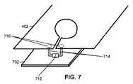
図5、図5A、および図6を再び参照すると、概略表現は、金属部分402に電気接続されたキャパシタC1を示す。いくつかの実施形態では、キャパシタC1は、金属部分402に直接接続され(たとえば、はんだ付けされ)得る。他の実施形態では、キャパシタC1を金属部分402に直接取り付けることは現実的でない場合がある。図7は、したがって、本開示の他の実施形態による、キャパシタC1を使用して金属部分402を同調する特定の実装形態の例を示す。電子デバイス(たとえば、図4Aの40)のデバイスエレクトロニクスを備えるプリント回路基板(PCB)702上に、同調要素712が配設され得る。PCB702に取り付けられ、同調要素712に接続されたコネクタ714(たとえば、ポゴピン)は、金属部分402上に形成された接触点716との電気的接触をするように同調要素712から伸びてよく、したがって同調要素712を金属部分402に電気接続する。Referring again to FIGS. 5, 5A and 6, the schematic representation shows capacitor C1 electrically connected to
様々な実施形態では、同調要素712は、どの適切な回路機構または回路要素であってもよい。いくつかの実施形態では、たとえば、同調要素712は、キャパシタC1(図5)などのキャパシタであってよい。他の実施形態では、同調要素712は、可変キャパシタ、直列接続キャパシタ、並列接続キャパシタなどを含むキャパシタのネットワークを含み得る。上で言及したように、金属部分402は、そのループ形状412(図4B)によって、それに関連付けられたインダクタンスLmodel(図5)を有する。いくつかの実施形態では、金属部分402のインダクタンスは変更され得る。したがって、いくつかの実施形態では、同調要素712は、金属部分402および同調要素712によって提示される総インダクタンスを増大または減少するための1つまたは複数の誘導性要素を含み得る。In various embodiments, tuning
本開示によると、金属部分402および電力受信要素502の役割は反対にしてよい。図8を参照すると、たとえば、いくつかの実施形態では、金属部分402は電力受信要素802として働き得る。整流器814は、回路812を画定するように、金属部分402に接続され得る。いくつかの実施形態では、同調キャパシタC1(または他の同調回路)が、たとえば、回路812の共振周波数を同調するように、回路812に追加され得る。磁場を生成するための手段は、開口408に巻き付けられた導電性材料のコイル804を含み得る。キャパシタC2が、コイル804およびキャパシタC2によって画定される回路の共振周波数を同調するように、コイル804に接続され得る。According to the present disclosure, the roles of the
上述したように、送信コイル(たとえば、電力送信要素114、図1)から電力受信要素802への電力伝達は、送信コイルと電力受信要素802との間の相互インダクタンスおよび/または電力受信要素802とコイル804との間の相互インダクタンスを制御することによって制御され得る。たとえば、電力受信要素802は、送信コイルと電力受信要素802との間の相互インダクタンスを改変するために、送信コイルによって生成された外部磁場の周波数に関して共振するか、または共振外になるように(たとえば、C1を同調することによって)同調され得る。同様に、コイル804は、電力受信要素802とコイル804との間の相互インダクタンスを改変するために、外部磁場の周波数に関して共振するか、または共振外になるように(たとえば、C2を同調することによって)同調され得る。As discussed above, the transfer of power from the transmit coil (eg, power transmit
図8Aを参照すると、他の実施形態では、コイル804は省かれてよく、電力受信要素802(金属部分402を使用して実現される)、ならびにキャパシタC1および整流器814を備える共振回路812のみを残す。Referring to FIG. 8A, in another embodiment,
図9および図9Aを参照すると、本開示による実施形態が、装着可能電子デバイスを含み得る。いくつかの実施形態では、たとえば、装着可能電子デバイス90は、締め具94に接続されたデバイス本体92を含み得る。装着可能電子デバイス90は、スマートウォッチ、フィットネス監視デバイスなどであってよい。 Referring to FIGS. 9 and 9A, embodiments according to the present disclosure may include wearable electronic devices. In some embodiments, for example, the wearable
デバイス本体92は、金属部分902を含み得る。金属部分902は、中央開口908と、開口908および金属部分902の周縁を接続するスロット910とを画定する開ループ形状を有し得る。キャパシタC1が、キャパシタC1によって同調される回路を画定するように、金属部分902に接続され得る。デバイス本体92は、開口908に巻き付けられた電力受信要素(たとえば、コイル)912を含み得る。電力受信要素912は、キャパシタC2に(たとえば、電力受信要素912を同調するように)、および外部生成磁場に露出されると、電力受信要素912中で誘導された電流のフローを使用してDC電圧Voutを生じるように、整流器904に接続され得る。
いくつかの実施形態では、金属部分902は、装着可能電子デバイス90を備えるデバイスエレクトロニクス(図示せず)を収容するためのハウジングとして働き得る。図9Aを参照すると、他の実施形態では、装着可能電子デバイス91が、金属部分902および電力受信要素912を収容するための非金属製ハウジング96を含み得るデバイス本体93を含み得る。 In some embodiments, the
上述したように、送信コイル(たとえば、電力送信要素114、図1)から電力受信要素912への電力伝達は、送信コイルと電力受信要素912との間の相互インダクタンスおよび/または電力受信要素912と金属部分902との間の相互インダクタンスを制御することによって制御され得る。たとえば、電力受信要素912は、送信コイルと電力受信要素912との間の相互インダクタンスを改変するために、送信コイルによって生成された外部磁場の周波数に関して共振するか、または共振外になるように(たとえば、C2を同調することによって)同調され得る。同様に、金属部分902は、電力受信要素912と金属部分902との間の相互インダクタンスを改変するために、外部磁場の周波数に関して共振するか、または共振外になるように(たとえば、C1を同調することによって)同調され得る。As discussed above, the transfer of power from the transmit coil (eg, power transmit
図10を参照すると、本開示による実施形態が、ポータブルコンピュータ、たとえば、ラップトップコンピュータ、コンピュータタブレットなどを含み得る。いくつかの実施形態では、たとえば、ポータブルコンピュータ10が、ディスプレイ1004およびデバイスエレクトロニクス(たとえば、回路機構、バッテリーなど)1006、ならびにワイヤレス電力受信機1010を収容するための前面エンクロージャ1002および背面エンクロージャ1008を備え得る。背面エンクロージャ1008は、ワイヤレス電力受信機能と干渉しないために、非金属製材料であってよい。本開示によるワイヤレス電力受信機1010の詳細について、ここで記載する。 Referring to FIG. 10, an embodiment in accordance with the present disclosure may include a portable computer, such as a laptop computer, a computer tablet, and the like. In some embodiments, for example,
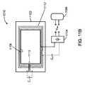
図11Aおよび図11Bは、本開示の実施形態によるワイヤレス電力受信機1010の詳細を示す概略表現である。ワイヤレス電力受信機1010は、開口1108、ならびに開口1108と金属部分1102の周縁との間に伸びるスロット1110を画定する開ループの形状を有する金属部分1102を含み得る。電力受信要素(たとえば、コイル)1112が、開口1108に巻き付けられ得る。整流器1104が、外部生成磁場に応答して電力受信要素1112中で起こり得る電流のフローからDC電圧Voutを生じるように、電力受信要素1112に接続され得る。11A and 11B are schematic representations showing details of a
電力受信機1010によって生成され得る磁場がデバイスエレクトロニクス1006に結合するのを防止するために、電力受信要素1112とデバイスエレクトロニクス1006との間にフェライトレイヤ1122が配設され得る。フェライトレイヤ1122は、金属部分1102の詳細をより明白に示すために、図11Bでは省かれている。 A
キャパシタC1が、金属部分1102と送信コイルとの間の相互インダクタンスを改変するために、金属部分1102を、外部生成磁場と共振するか、または外部生成磁場と共振しないように同調するのに使用され得る。同様に、キャパシタC2が、電力受信要素1112と金属部分1102との間の相互インダクタンスを改変するために、電力受信要素1112を、外部生成磁場と共振するか、または共振しないように同調するのに使用され得る。Capacitor C1 is used to tune
本開示の実施形態によると、電力受信機1010は、図10に示すポータブルコンピュータ10のエリアよりも小さいエリアを有し得る。いくつかの実施形態では、電力受信機1010のエリアは、ポータブルコンピュータ10のエリアの50%未満であり得る。同調金属部分1102の増幅効果により、コイル1112は、外部生成磁場により強く結合し、したがって、同調金属部分1112などの増幅要素を使用しないワイヤレス電力伝達システムにおけるよりも大きい電力伝達を達成し得る。したがって、電力受信機1010は、より小さくてよく、それでも、より大きいワイヤレス電力伝達システムと比較して、同様の電力伝達を達成し得る。 According to embodiments of the present disclosure,
上記の説明は、特定の実施形態の態様がどのように実装される場合があるかの例とともに、本開示の様々な実施形態を示す。上記の例は、唯一の実施形態であると見なすべきではなく、これらは、以下の特許請求の範囲によって規定されるような特定の実施形態の融通性および利点を例示するために提示される。上記の開示および以下の特許請求の範囲に基づいて、特許請求の範囲によって規定される本開示の範囲から逸脱することなく、他の構成、実施形態、実施態様、および等価物が採用されてよい。 The above description illustrates various embodiments of the present disclosure, with examples of how aspects of particular embodiments may be implemented. The above examples should not be considered as the only embodiments, which are presented to illustrate the flexibility and advantages of particular embodiments as defined by the following claims. Based on the above disclosure and the following claims, other configurations, embodiments, implementations and equivalents may be employed without departing from the scope of the present disclosure as defined by the claims. .
10 ポータブルコンピュータ
40 電子デバイス
90 装着可能電子デバイス
91 装着可能電子デバイス
92 デバイス本体
93 デバイス本体
94 締め具
96 非金属製ハウジング
100 ワイヤレス電力伝達システム
104 送信機
105 ワイヤレス場
108 受信機
114 電力送信要素
118 電力受信要素
200 ワイヤレス電力伝達システム、システム
204 送信機
205 ワイヤレス場
206 送信回路機構
208 受信機、ワイヤレス電力受信機
210 受信回路機構
214 電力送信要素
218 電力受信要素
219 通信チャネル
222 発振器
223 周波数制御信号
224 ドライバ回路
226 フロントエンド回路
232 フロントエンド回路
234 整流器回路
236 バッテリー
240 コントローラ、送信コントローラ
250 コントローラ
350 送信または受信回路機構、送信および/または受信回路機構、回路機構
352 電力送信または受信要素
354 キャパシタ
356 キャパシタ
358 信号
360 同調回路
400 背面エンクロージャ(ハウジング)
402 金属部分、部分
402a 金属部分、部分
402b 金属部分、部分
404 空間、ギャップ
406 ギャップ
408 開口
410 スロット
412 開ループ、ループ形状
422 電流フロー
502 電力受信要素
504 整流器
506 負荷
512 回路
604 誘導磁場、影付きエリア
606 電流
702 プリント回路基板(PCB)
712 同調要素
714 コネクタ
716 接触点
802 電力受信要素
804 コイル
812 回路、共振回路
814 整流器
902 金属部分
904 整流器
908 中央開口、開口
910 スロット
912 電力受信要素
1002 前面エンクロージャ
1004 ディスプレイ
1006 デバイスエレクトロニクス
1008 背面エンクロージャ
1010 ワイヤレス電力受信機、電力受信機
1102 金属部分
1104 整流器
1006 デバイスエレクトロニクス
1108 開口
1110 スロット
1112 電力受信要素、コイル、同調金属部分
1122 フェライトレイヤ10 portable computers
40 electronic devices
90 Wearable Electronic Devices
91 Wearable Electronic Devices
92 Device body
93 Device body
94 Fasteners
96 Non-metallic housing
100 Wireless Power Transfer System
104 transmitter
105 Wireless Field
108 Receiver
114 power transmission element
118 Power receiving element
200 Wireless Power Transfer System, System
204 transmitter
205 Wireless Field
206 Transmission circuit
208 receiver, wireless power receiver
210 Receiver circuitry
214 Power transmission element
218 Power receiving element
219 communication channel
222 Oscillator
223 frequency control signal
224 driver circuit
226 front end circuit
232 front end circuit
234 Rectifier Circuit
236 Battery
240 controller, transmit controller
250 controller
350 transmit or receive circuitry, transmit and / or receive circuitry, circuitry
352 Power transmit or receive element
354 capacitor
356 capacitor
358 signals
360 tuning circuit
400 rear enclosure (housing)
402 Metal parts, parts
402a metal parts, parts
402b metal parts, parts
404 space, gap
406 gap
408 opening
410 slots
412 Open loop, loop shape
422 current flow
502 Power receiving element
504 Rectifier
506 load
512 circuits
604 Induced magnetic field, shaded area
606 current
702 Printed Circuit Board (PCB)
712 tuning element
714 connector
716 contact points
802 Power receiving element
804 coil
812 circuit, resonant circuit
814 Rectifier
902 Metal part
904 Rectifier
908 Central opening, opening
910 slots
912 Power receiving element
1002 front enclosure
1004 Display
1006 Device Electronics
1008 rear enclosure
1010 Wireless Power Receiver, Power Receiver
1102 Metal part
1104 Rectifier
1006 Device Electronics
1108 opening
1110 slots
1112 Power receiving element, coil, tuning metal part
1122 Ferrite layer
Claims (30)
Translated fromJapanese第1の磁場に磁気結合するように構成された導電体と、
前記導電体に電気接続された第1の同調要素と、
前記導電体によって画定された開口に巻き付けられた導電性コイルであって、第2の磁場に磁気結合するように構成された、導電性コイルと
を備える、装置。An electronic device for wireless power transfer,
A conductor configured to magnetically couple to the first magnetic field;
A first tuning element electrically connected to the conductor;
A conductive coil wound around an opening defined by the conductor, the conductive coil configured to magnetically couple to a second magnetic field.
前記第1の同調要素を前記導電体に電気接続するコネクタと
をさらに備える、請求項1に記載の装置。A printed circuit board on which the first tuning element is disposed;
The apparatus of claim 1, further comprising a connector electrically connecting the first tuning element to the electrical conductor.
前記電子デバイスのためのハウジングを備える導電性構造を介して外部生成磁場に磁気結合して、前記導電性構造から発出する誘導磁場を生じるステップと、
電力受信要素を介して前記誘導磁場に磁気結合して、前記電力受信要素中で電流を誘導するステップであって、前記電力受信要素は、前記導電性構造から電気的に絶縁される、ステップと、
前記電力受信要素中で誘導された前記電流から電力を生じるステップと
を含む、方法。A method for wireless power transfer to an electronic device, comprising:
Magnetically coupling to an externally generated magnetic field via a conductive structure comprising a housing for the electronic device to produce an induced magnetic field emanating from the conductive structure;
Magnetically coupling to the inductive magnetic field via a power receiving element to induce a current in the power receiving element, the power receiving element being electrically isolated from the conductive structure ,
Generating power from the current induced in the power receiving element.
前記装置を備える電子構成要素を封入するように構成されたハウジングであって、金属部分を備える、ハウジングと、
前記ハウジングの前記金属部分に接続された第1の同調要素であって、前記ハウジングの前記金属部分は、外部生成磁場に磁気結合されたことに応答して、電流のフローをその中で誘導させることを可能にする形状を有し、前記電流のフローに応答して、前記金属部分から誘導磁場が発出する、第1の同調要素と、
導電性コイルであって、前記誘導磁場に磁気結合されたことに応答して、前記導電性コイル中で電流のフローが誘導される、導電性コイルと、
負荷に電力を供給するために、前記導電性コイル中で誘導される電流を整流するように構成された整流器と
を備える、装置。An apparatus for wirelessly receiving power,
A housing configured to enclose an electronic component comprising the device, the housing comprising a metal part;
A first tuning element connected to the metal portion of the housing, wherein the metal portion of the housing induces current flow therein in response to being magnetically coupled to an externally generated magnetic field A first tuning element having a shape that makes it possible to generate an induced magnetic field from the metal part in response to the flow of the current;
A conductive coil, in response to being magnetically coupled to the inductive magnetic field, a flow of current is induced in the conductive coil;
And a rectifier configured to rectify a current induced in the conductive coil to provide power to a load.
前記電子デバイスの電子機器を収容するための手段であって、外部生成磁場に磁気結合するための手段から発出する誘導磁場を生じるように、前記外部生成磁場に磁気結合するための前記手段を備える金属部分を有し、前記外部生成磁場に磁気結合するための前記手段は、共振周波数で共振するように、前記外部生成磁場に磁気結合するための前記手段を同調するための手段に電気接続される、手段と、
電流を誘導するために前記誘導磁場に磁気結合するための手段であって、前記外部生成磁場に磁気結合するための前記手段から電気的に絶縁された、手段と、
前記誘導磁場に磁気結合するための前記手段において誘導された前記電流から電力を生じるための手段と
を備える、装置。An apparatus for wirelessly receiving power at an electronic device, the apparatus comprising:
Means for housing the electronics of the electronic device, the means for magnetically coupling to the externally generated magnetic field to produce an induced magnetic field emanating from the means for magnetically coupling to the externally generated magnetic field The means for magnetically coupling to the externally generated magnetic field is electrically connected to the means for magnetically coupling to the externally generated magnetic field so as to be resonant at a resonant frequency. Means, and
Means for magnetically coupling to the induced magnetic field to induce an electrical current, the means electrically isolated from the means for magnetically coupling to the externally generated magnetic field;
Means for producing power from the current induced in the means for magnetic coupling to the induced magnetic field.
Applications Claiming Priority (5)
| Application Number | Priority Date | Filing Date | Title |
|---|---|---|---|
| US201662288685P | 2016-01-29 | 2016-01-29 | |
| US62/288,685 | 2016-01-29 | ||
| US15/231,325 | 2016-08-08 | ||
| US15/231,325US10333334B2 (en) | 2016-01-29 | 2016-08-08 | Wireless power transfer in an electronic device having a tuned metallic body |
| PCT/US2017/012072WO2017131931A1 (en) | 2016-01-29 | 2017-01-04 | Wireless power transfer in an electronic device having a tuned metallic body |
Publications (2)
| Publication Number | Publication Date |
|---|---|
| JP2019512197Atrue JP2019512197A (en) | 2019-05-09 |
| JP2019512197A5 JP2019512197A5 (en) | 2020-02-06 |
Family
ID=59385744
Family Applications (1)
| Application Number | Title | Priority Date | Filing Date |
|---|---|---|---|
| JP2018538814APendingJP2019512197A (en) | 2016-01-29 | 2017-01-04 | Wireless power transfer in an electronic device having a tuning metal |
Country Status (8)
| Country | Link |
|---|---|
| US (2) | US10333334B2 (en) |
| EP (1) | EP3408915B1 (en) |
| JP (1) | JP2019512197A (en) |
| KR (1) | KR20180105655A (en) |
| CN (1) | CN108684208A (en) |
| AU (1) | AU2017211647B2 (en) |
| TW (1) | TW201801445A (en) |
| WO (2) | WO2017131916A1 (en) |
Families Citing this family (5)
| Publication number | Priority date | Publication date | Assignee | Title |
|---|---|---|---|---|
| US10333334B2 (en) | 2016-01-29 | 2019-06-25 | Qualcomm Incorporated | Wireless power transfer in an electronic device having a tuned metallic body |
| US10505254B2 (en)* | 2017-07-28 | 2019-12-10 | Stmicroelectronics, Inc. | Antenna design for active load modulation in a near field communication transponder device |
| US10462417B2 (en)* | 2017-08-31 | 2019-10-29 | Apple Inc. | Methods and apparatus for reducing electromagnetic interference resultant from data transmission over a high-speed audio/visual interface |
| US10629533B2 (en)* | 2018-03-13 | 2020-04-21 | Toshiba Memory Corporation | Power island segmentation for selective bond-out |
| CN117278077A (en)* | 2022-06-14 | 2023-12-22 | 台湾东电化股份有限公司 | Wireless transmission module |
Citations (5)
| Publication number | Priority date | Publication date | Assignee | Title |
|---|---|---|---|---|
| WO2009031639A1 (en)* | 2007-09-06 | 2009-03-12 | Showa Denko K.K. | Non-contact charge type accumulator |
| JP2012525816A (en)* | 2009-04-28 | 2012-10-22 | クアルコム,インコーポレイテッド | Parasitic device for wireless power transfer |
| JP2014090585A (en)* | 2012-10-30 | 2014-05-15 | Canon Inc | Electronic device, control method, and computer program |
| WO2014167881A1 (en)* | 2013-04-08 | 2014-10-16 | 株式会社村田製作所 | Communication terminal |
| US20150380827A1 (en)* | 2013-02-22 | 2015-12-31 | Nokia Technologies Oy | Apparatus and methods for wireless coupling |
Family Cites Families (36)
| Publication number | Priority date | Publication date | Assignee | Title |
|---|---|---|---|---|
| US7521890B2 (en) | 2005-12-27 | 2009-04-21 | Power Science Inc. | System and method for selective transfer of radio frequency power |
| US8855554B2 (en)* | 2008-03-05 | 2014-10-07 | Qualcomm Incorporated | Packaging and details of a wireless power device |
| US20160087687A1 (en) | 2008-09-27 | 2016-03-24 | Witricity Corporation | Communication in a wireless power transmission system |
| US8907531B2 (en) | 2008-09-27 | 2014-12-09 | Witricity Corporation | Wireless energy transfer with variable size resonators for medical applications |
| US20120242159A1 (en) | 2008-09-27 | 2012-09-27 | Herbert Toby Lou | Multi-resonator wireless energy transfer for appliances |
| US20120112691A1 (en) | 2008-09-27 | 2012-05-10 | Kurs Andre B | Wireless energy transfer for vehicles |
| US20120248981A1 (en) | 2008-09-27 | 2012-10-04 | Aristeidis Karalis | Multi-resonator wireless energy transfer for lighting |
| AU2010213557A1 (en) | 2009-02-13 | 2011-09-01 | Witricity Corporation | Wireless energy transfer in lossy environments |
| US9088307B2 (en)* | 2010-12-29 | 2015-07-21 | National Semiconductor Corporation | Non-resonant and quasi-resonant system for wireless power transmission to multiple receivers |
| JP2012143146A (en)* | 2011-01-03 | 2012-07-26 | Samsung Electronics Co Ltd | Wireless power transmission apparatus and wireless power transmission system thereof |
| CA2868986C (en) | 2011-03-30 | 2021-07-27 | Ambature Inc. | Electrical, mechanical, computing, and/or other devices formed of extremely low resistance materials |
| US9496755B2 (en) | 2011-09-26 | 2016-11-15 | Qualcomm Incorporated | Systems, methods, and apparatus for rectifier filtering for input waveform shaping |
| US20130127252A1 (en) | 2011-11-17 | 2013-05-23 | William S. Yerazunis | Wireless Energy Transfer with Perfect Magnetic Conductors |
| US9225388B2 (en) | 2012-07-03 | 2015-12-29 | Intel Corporation | Transmitting magnetic field through metal chassis using fractal surfaces |
| CN105051304A (en) | 2012-07-25 | 2015-11-11 | 总锁有限责任公司 | Integrated antenna coil in a metallic body |
| DE112013000735T5 (en)* | 2012-12-20 | 2014-11-06 | Murata Manufacturing Co., Ltd. | Information terminal apparatus |
| US9876535B2 (en) | 2013-02-21 | 2018-01-23 | Qualcomm Incorporated | Modular inductive power transfer power supply and method of operation |
| US9431169B2 (en) | 2013-06-07 | 2016-08-30 | Qualcomm Incorporated | Primary power supply tuning network for two coil device and method of operation |
| US20150009077A1 (en)* | 2013-07-03 | 2015-01-08 | Samsung Electronics Co., Ltd. | Cover of a mobile device and mobile device including the same |
| WO2015041066A1 (en)* | 2013-09-17 | 2015-03-26 | 株式会社村田製作所 | Camera module, and electronic apparatus |
| US10147538B2 (en) | 2013-11-08 | 2018-12-04 | Nokia Technologies Oy | Coil arrangement |
| CN103560598A (en)* | 2013-11-12 | 2014-02-05 | 天津工业大学 | Enhanced type electromagnetic resonance subway wireless power supply system |
| US9461500B2 (en) | 2013-11-21 | 2016-10-04 | Htc Corporation | Wireless charging receiving device and wireless charging system using the same |
| JP6297863B2 (en)* | 2014-03-03 | 2018-03-20 | Ihi運搬機械株式会社 | Non-contact power feeding system and vehicle power feeding device |
| US9730002B2 (en) | 2014-04-10 | 2017-08-08 | Avago Technologies General Ip (Singapore) Pte. Ltd. | Mechanical enclosures for a communication device |
| US10381875B2 (en) | 2014-07-07 | 2019-08-13 | Qualcomm Incorporated | Wireless power transfer through a metal object |
| US20160111889A1 (en) | 2014-10-20 | 2016-04-21 | Qualcomm Incorporated | Segmented conductive back cover for wireless power transfer |
| CN104333149B (en) | 2014-11-13 | 2017-03-01 | 矽力杰半导体技术(杭州)有限公司 | Tuning circuit, tuning methods and mode of resonance contactless power supply device |
| US10581284B2 (en) | 2014-12-16 | 2020-03-03 | Samsung Electronics Co., Ltd. | Wireless charger and wireless power receiver |
| CN104821667B (en)* | 2015-03-16 | 2017-02-22 | 中国计量学院 | Magnetic coupling resonant wireless electric energy transmission device based on low frequency PWM rectifier |
| US10476304B2 (en) | 2015-05-27 | 2019-11-12 | Qualcomm Incorporated | Wireless power receive coil for metal backed device |
| CN105119036B (en) | 2015-09-18 | 2019-03-15 | 深圳市信维通信股份有限公司 | A kind of near-field communication and wireless charging integral antenna based on metal rear shell |
| US10361588B2 (en) | 2015-12-07 | 2019-07-23 | Qualcomm Incorporated | Coupled resonator in a metal back cover |
| US20170170689A1 (en) | 2015-12-14 | 2017-06-15 | Qualcomm Incorporated | Wireless charging of metal framed electronic devices |
| US10333334B2 (en)* | 2016-01-29 | 2019-06-25 | Qualcomm Incorporated | Wireless power transfer in an electronic device having a tuned metallic body |
| US9827430B1 (en) | 2017-02-02 | 2017-11-28 | Qualcomm Incorporated | Injected conductive tattoos for powering implants |
- 2016
- 2016-08-08USUS15/231,325patent/US10333334B2/enactiveActive
- 2016-09-14USUS15/265,395patent/US10312716B2/enactiveActive
- 2016-12-28WOPCT/US2016/068829patent/WO2017131916A1/ennot_activeCeased
- 2017
- 2017-01-04AUAU2017211647Apatent/AU2017211647B2/enactiveActive
- 2017-01-04WOPCT/US2017/012072patent/WO2017131931A1/ennot_activeCeased
- 2017-01-04KRKR1020187021255Apatent/KR20180105655A/ennot_activeWithdrawn
- 2017-01-04EPEP17700587.3Apatent/EP3408915B1/enactiveActive
- 2017-01-04CNCN201780008384.3Apatent/CN108684208A/enactivePending
- 2017-01-04JPJP2018538814Apatent/JP2019512197A/enactivePending
- 2017-01-13TWTW106101116Apatent/TW201801445A/enunknown
Patent Citations (5)
| Publication number | Priority date | Publication date | Assignee | Title |
|---|---|---|---|---|
| WO2009031639A1 (en)* | 2007-09-06 | 2009-03-12 | Showa Denko K.K. | Non-contact charge type accumulator |
| JP2012525816A (en)* | 2009-04-28 | 2012-10-22 | クアルコム,インコーポレイテッド | Parasitic device for wireless power transfer |
| JP2014090585A (en)* | 2012-10-30 | 2014-05-15 | Canon Inc | Electronic device, control method, and computer program |
| US20150380827A1 (en)* | 2013-02-22 | 2015-12-31 | Nokia Technologies Oy | Apparatus and methods for wireless coupling |
| WO2014167881A1 (en)* | 2013-04-08 | 2014-10-16 | 株式会社村田製作所 | Communication terminal |
Also Published As
| Publication number | Publication date |
|---|---|
| CN108684208A (en) | 2018-10-19 |
| US10312716B2 (en) | 2019-06-04 |
| EP3408915B1 (en) | 2022-03-16 |
| BR112018015387A2 (en) | 2018-12-18 |
| US20170222481A1 (en) | 2017-08-03 |
| TW201801445A (en) | 2018-01-01 |
| US20170222467A1 (en) | 2017-08-03 |
| AU2017211647A1 (en) | 2018-07-19 |
| WO2017131931A1 (en) | 2017-08-03 |
| EP3408915A1 (en) | 2018-12-05 |
| US10333334B2 (en) | 2019-06-25 |
| AU2017211647B2 (en) | 2020-08-20 |
| KR20180105655A (en) | 2018-09-28 |
| WO2017131916A1 (en) | 2017-08-03 |
Similar Documents
| Publication | Publication Date | Title |
|---|---|---|
| US9742203B2 (en) | Distributed resonators for wireless power transfer | |
| CN107408823B (en) | Multi-turn coil on metal backboard | |
| JP6612863B2 (en) | Segmented conductive back cover for wireless power transfer | |
| AU2017211647B2 (en) | Wireless power transfer in an electronic device having a tuned metallic body | |
| US20170093172A1 (en) | Multiple-axis wireless power receiver | |
| US10361588B2 (en) | Coupled resonator in a metal back cover | |
| US20170155282A1 (en) | Enhanced coupling in a wearable resonator | |
| HK1257336A1 (en) | Wireless power transfer in an electronic device having a tuned metallic body | |
| US20170229913A1 (en) | Wireless power transfer in wearable devices | |
| BR112018015387B1 (en) | WIRELESS ENERGY TRANSFER IN AN ELECTRONIC DEVICE WITH A TUNE METAL BODY |
Legal Events
| Date | Code | Title | Description |
|---|---|---|---|
| A521 | Request for written amendment filed | Free format text:JAPANESE INTERMEDIATE CODE: A523 Effective date:20180731 | |
| A521 | Request for written amendment filed | Free format text:JAPANESE INTERMEDIATE CODE: A523 Effective date:20191218 | |
| A621 | Written request for application examination | Free format text:JAPANESE INTERMEDIATE CODE: A621 Effective date:20191218 | |
| A977 | Report on retrieval | Free format text:JAPANESE INTERMEDIATE CODE: A971007 Effective date:20201216 | |
| A131 | Notification of reasons for refusal | Free format text:JAPANESE INTERMEDIATE CODE: A131 Effective date:20210104 | |
| A02 | Decision of refusal | Free format text:JAPANESE INTERMEDIATE CODE: A02 Effective date:20210802 |