JP2019512196A - Memister-based logic gate - Google Patents
Memister-based logic gateDownload PDFInfo
- Publication number
- JP2019512196A JP2019512196AJP2018562725AJP2018562725AJP2019512196AJP 2019512196 AJP2019512196 AJP 2019512196AJP 2018562725 AJP2018562725 AJP 2018562725AJP 2018562725 AJP2018562725 AJP 2018562725AJP 2019512196 AJP2019512196 AJP 2019512196A
- Authority
- JP
- Japan
- Prior art keywords
- memristor
- output
- gate
- logic
- xor
- Prior art date
- Legal status (The legal status is an assumption and is not a legal conclusion. Google has not performed a legal analysis and makes no representation as to the accuracy of the status listed.)
- Granted
Links
Images


Classifications
- G—PHYSICS
- G06—COMPUTING OR CALCULATING; COUNTING
- G06F—ELECTRIC DIGITAL DATA PROCESSING
- G06F7/00—Methods or arrangements for processing data by operating upon the order or content of the data handled
- G06F7/38—Methods or arrangements for performing computations using exclusively denominational number representation, e.g. using binary, ternary, decimal representation
- G06F7/48—Methods or arrangements for performing computations using exclusively denominational number representation, e.g. using binary, ternary, decimal representation using non-contact-making devices, e.g. tube, solid state device; using unspecified devices
- G06F7/50—Adding; Subtracting
- G06F7/501—Half or full adders, i.e. basic adder cells for one denomination
- G—PHYSICS
- G11—INFORMATION STORAGE
- G11C—STATIC STORES
- G11C11/00—Digital stores characterised by the use of particular electric or magnetic storage elements; Storage elements therefor
- G11C11/56—Digital stores characterised by the use of particular electric or magnetic storage elements; Storage elements therefor using storage elements with more than two stable states represented by steps, e.g. of voltage, current, phase, frequency
- G11C11/5685—Digital stores characterised by the use of particular electric or magnetic storage elements; Storage elements therefor using storage elements with more than two stable states represented by steps, e.g. of voltage, current, phase, frequency using storage elements comprising metal oxide memory material, e.g. perovskites
- G—PHYSICS
- G11—INFORMATION STORAGE
- G11C—STATIC STORES
- G11C13/00—Digital stores characterised by the use of storage elements not covered by groups G11C11/00, G11C23/00, or G11C25/00
- G11C13/0002—Digital stores characterised by the use of storage elements not covered by groups G11C11/00, G11C23/00, or G11C25/00 using resistive RAM [RRAM] elements
- G11C13/0007—Digital stores characterised by the use of storage elements not covered by groups G11C11/00, G11C23/00, or G11C25/00 using resistive RAM [RRAM] elements comprising metal oxide memory material, e.g. perovskites
- H—ELECTRICITY
- H03—ELECTRONIC CIRCUITRY
- H03K—PULSE TECHNIQUE
- H03K19/00—Logic circuits, i.e. having at least two inputs acting on one output; Inverting circuits
- H03K19/0175—Coupling arrangements; Interface arrangements
- H03K19/017509—Interface arrangements
- H—ELECTRICITY
- H03—ELECTRONIC CIRCUITRY
- H03K—PULSE TECHNIQUE
- H03K19/00—Logic circuits, i.e. having at least two inputs acting on one output; Inverting circuits
- H03K19/02—Logic circuits, i.e. having at least two inputs acting on one output; Inverting circuits using specified components
- H03K19/173—Logic circuits, i.e. having at least two inputs acting on one output; Inverting circuits using specified components using elementary logic circuits as components
- H—ELECTRICITY
- H03—ELECTRONIC CIRCUITRY
- H03K—PULSE TECHNIQUE
- H03K19/00—Logic circuits, i.e. having at least two inputs acting on one output; Inverting circuits
- H03K19/20—Logic circuits, i.e. having at least two inputs acting on one output; Inverting circuits characterised by logic function, e.g. AND, OR, NOR, NOT circuits
- H03K19/21—EXCLUSIVE-OR circuits, i.e. giving output if input signal exists at only one input; COINCIDENCE circuits, i.e. giving output only if all input signals are identical
- H—ELECTRICITY
- H10—SEMICONDUCTOR DEVICES; ELECTRIC SOLID-STATE DEVICES NOT OTHERWISE PROVIDED FOR
- H10N—ELECTRIC SOLID-STATE DEVICES NOT OTHERWISE PROVIDED FOR
- H10N70/00—Solid-state devices having no potential barriers, and specially adapted for rectifying, amplifying, oscillating or switching
- H10N70/20—Multistable switching devices, e.g. memristors
- H—ELECTRICITY
- H10—SEMICONDUCTOR DEVICES; ELECTRIC SOLID-STATE DEVICES NOT OTHERWISE PROVIDED FOR
- H10N—ELECTRIC SOLID-STATE DEVICES NOT OTHERWISE PROVIDED FOR
- H10N70/00—Solid-state devices having no potential barriers, and specially adapted for rectifying, amplifying, oscillating or switching
- H10N70/801—Constructional details of multistable switching devices
- H10N70/881—Switching materials
- H10N70/883—Oxides or nitrides
Landscapes
- Engineering & Computer Science (AREA)
- Physics & Mathematics (AREA)
- Computer Hardware Design (AREA)
- Computing Systems (AREA)
- General Engineering & Computer Science (AREA)
- Mathematical Physics (AREA)
- General Physics & Mathematics (AREA)
- Mathematical Analysis (AREA)
- Computational Mathematics (AREA)
- Pure & Applied Mathematics (AREA)
- Theoretical Computer Science (AREA)
- Chemical & Material Sciences (AREA)
- Materials Engineering (AREA)
- Mathematical Optimization (AREA)
- Metal-Oxide And Bipolar Metal-Oxide Semiconductor Integrated Circuits (AREA)
- Logic Circuits (AREA)
- Semiconductor Integrated Circuits (AREA)
Abstract
Translated fromJapaneseDescription
Translated fromJapanese本発明は、少なくとも1つのメモリスタが論理ゲートアーキテクチャに使用される、論理ゲート、又は複数論理ゲートに関する。 The present invention relates to logic gates or multiple logic gates, wherein at least one memristor is used in a logic gate architecture.
メモリスタ(「メモリ・レジスタ」の略)は、将来性の高いナノスケール・プログラマブル抵抗メモリ装置として現れている。かかる装置は、高密度不揮発メモリ、物理的複製防止機能(physically uncloneable function: PUFs、又は「パフ」)、神経形態学的システム、及び論理設計などの分野に、既に用途を見いだしている。 Memristor (abbreviation "memory register") is emerging as a promising nanoscale programmable resistive memory device. Such devices have already found use in areas such as high density non-volatile memory, physically uncloneable functions (PUFs, or "puffs"), neuromorphic systems, and logic design.
しかしながら、既存のメモリスタベースの論理アーキテクチャの多くは、マルチプルクロック周期で動作し、演算用の複雑な制御論理を必要とする。その結果、これらは、既存のCMOS技術との統合は容易ではなく、既存のアーキテクチャと互換性の無い複雑な制御回路を要求する。さらに、CMOSの容量は、CMOSベースのシステムにおける不十分な上限限界をより高周波数に設定する阻害要因である。論理ゲート回路の電力消費を減らし、かつチップ面積利用を改善するという課題も存在する。 However, many existing memristor-based logic architectures operate on multiple clock cycles and require complex control logic for operations. As a result, they are not easy to integrate with existing CMOS technology and require complex control circuits that are not compatible with existing architectures. Furthermore, CMOS capacitance is a limiting factor that sets the upper limit inadequate for CMOS based systems to higher frequencies. There is also the problem of reducing the power consumption of the logic gate circuit and improving the chip area utilization.
本発明は、上記課題の観点から発明された。 The present invention was invented from the viewpoint of the above-mentioned subject.
本発明の論理ゲートは、第1入力部及び第2入力部と、各が正極端子及び負極端子を有する第1メモリスタ、第2メモリスタ、第3メモリスタ及び第4メモリスタと、第1出力部及び第2出力部と、を備える。 The logic gate according to the present invention includes a first memory, a second memory, a third memory, a fourth memory, a first output, and a first memory, each having a positive terminal and a negative terminal. And 2 output units.
第1メモリスタの負極端子と第2メモリスタの正極端子とは、共通に第1入力部に接続される。第3メモリスタの負極端子と、第4メモリスタの正極端子とは、第2入力部に共通に接続される。第2メモリスタの負極端子と、第4メモリスタの負極端子とは、第1出力部に共通に接続される。第1メモリスタの正極端子と、第3メモリスタの正極端子とは、第2出力部に共通に接続される。 The negative terminal of the first memristor and the positive terminal of the second memristor are commonly connected to the first input. The negative terminal of the third memristor and the positive terminal of the fourth memristor are commonly connected to the second input unit. The negative terminal of the second memristor and the negative terminal of the fourth memristor are commonly connected to the first output unit. The positive terminal of the first memristor and the positive terminal of the third memristor are commonly connected to the second output unit.
使用するときは、出力部の少なくとも一方の電圧、則ち、第1及び第2出力部間の電位差は、第1及び第2入力部に印加された電圧に対する論理演算に相当する。 When used, the voltage of at least one of the outputs, ie the potential difference between the first and second outputs, corresponds to a logical operation on the voltage applied to the first and second inputs.
本発明のさらなる概念は、従属請求項において定義される。 Further concepts of the invention are defined in the dependent claims.
本発明の実施の形態を、図面を参照して記載する。 Embodiments of the present invention will be described with reference to the drawings.
装置を流れる電流によって電気抵抗が変化する装置として、当該分野では、メモリスタが知られている。抵抗は、最小値RONと最大値ROFFとを有する。抵抗は、切り替えられ、また不揮発であるので(抵抗値は「記憶される」)、メモリスタは、メモリ素子として使用できる。図1は、メモリスタの記号を示す。本実施の形態では、斜線領域は「正極」端子2を示し、他方の端子4は「負極」端子である。正極端子2及び負極端子4に印加される電圧は、それぞれVp、Vnである。メモリスタは、Vp−Vn>VMのとき、低抵抗RONに切り替わる。なお、VMは、メモリスタ(メモリスタ装置)に固有な閾値であり、それ以外は、高抵抗ROFFに切り替わる。本明細書で使用される「正極」及び「負極」の言葉は、メモリスタの端子を区別し、また、上記スイッチング動作を定義するラベルである。当該分野において、端子は、イン・アウト、活性・不活性、入力・出力、±等の他のラベルとしても使用されることがある。A memristor is known in the art as a device whose electrical resistance changes due to the current flowing through the device. The resistor has a minimum value RON and a maximum value ROFF . Because resistors are switched and are non-volatile (resistance values are "stored"), memristor can be used as a memory element. FIG. 1 shows the symbol of memristor. In the present embodiment, the shaded area indicates the "positive electrode" terminal 2, and the
メモリスタは、TiO2(例えば、ドープ領域及びアンドープ領域、並びにPt電極)、Ag/Ag5In5Sb60Te30/Ta; Ag-a-LSMO-Pt (アモルファス亜マンガン酸塩薄膜中のAg ナノフィラメント)、及び他の強誘電体及びドープト重合材料などの様々な材料から作製される。本発明の実施の形態は、メモリスタの特性があるならば、特定の材料に限定されない。しかしながら、実施の形態によっては、必要とされる材料及び電圧は、CMOSエレクトロニクスと互換性を有する。Memisters can be made of TiO2 (eg, doped and undoped regions, and Pt electrodes), Ag / Ag5 In5 Sb60 Te30 / Ta; Ag-a-LSMO-Pt (Ag nanolayers in amorphous manganite thin films) It is made of various materials such as filaments) and other ferroelectric and doped polymeric materials. The embodiment of the present invention is not limited to a specific material as long as it has the characteristics of memristor. However, depending on the embodiment, the required materials and voltages are compatible with CMOS electronics.
本発明の第1の実施の形態は、図2に示されるような純粋メモリスタXORアーキテクチャ10である。XORアーキテクチャは、4つのメモリスタM1,M2,M3,M4を含む。第1メモリスタM1の負極端子と第2メモリスタM2の正極端子とは、共通に(PT)第1入力部Aに接続されている。第3メモリスタM3の負極端子と第4メモリスタM4の正極端子とは、共通に(PB)第2入力部Bに接続されている。第2メモリスタM2の負極端子と第4メモリスタM4の負極端子とは、共通に(PR)第1出力部12に接続されている。第1メモリスタM1の正極端子と第3メモリスタM3の正極端子とは、共通に(PL)第2出力部14に接続されている。第1及び第2出力部12、14に現れる電圧を、それぞれVL1、VL2と表す。The first embodiment of the present invention is a pure
表1に要約するように、VL1及びVL2の間の電位差、則ちは、仮想負荷抵抗RLの両端に現れる電圧は、入力部A及びBに印加される入力電圧に対してXOR演算のように振る舞う。この場合、入力電圧は、low、則ちOFF論理状態に対する0V、及びhigh、則ちON論理状態に対する+V1のうちのいずれかである。この表において、V1>VMであり、CMOS論理回路におけるVDDに等価であると仮定され、ON状態電圧を表す。これを主題1に説明する。
テーマ1: 図2の純粋メモリスタ回路は、表1に示されるXOR機能を実現する。
列1:回路には電流が流れない。
列2:この場合、Aを介したM2の正極端子の電圧は0Vであり、V1VがBを介したM3の負極端子に現れるため、メモリスタM2=M3=ROFFである。これに対して、メモリスタM4,M1は、正極端子がV1Vに近く、負極端子が0Vに近いため、メモリスタM4=M1=RONになる。分圧のために、PRでの電圧は、V1Vに上昇し、PLでの電圧は0Vに向けて降下する。ここで、電流は、B→PB→PR→VL1→VL2→PL→PT→Aの順に流れる。故に、これが論理1である。
列3:これは、列2に類似する。この場合、M1=M4=ROFF、一方、M2=M3=RONになる。PRの電圧がV1Vに向けて上昇し、PLの電圧は0Vに向けて降下する。電流は、A→PT→PR→VL1→VL2→PL→PB→Aの順に流れる。故に、これが論理1である。
列4:この場合、PL(VL2)及びPR(VL1)の両方が同一電圧レベルであり、RLを流れる電流はない。故に、これが論理0(ゼロ)である。As summarized in Table 1, the potential difference between VL1 and VL2 , ie, the voltage appearing across the virtual load resistance RL , XOR's the input voltage applied to the inputs A and B Behave like. In this case, the input voltage is either low, 0V for the OFF logic state, and high, ie + V1 for the ON logic state. In this table, it is assumed that V1 > VM , which is assumed to be equivalent to VDD in the CMOS logic circuit, and represents the ON state voltage. This will be described in subject 1.
Theme 1: The pure memristor circuit of FIG. 2 implements the XOR function shown in Table 1.
Column 1: no current flows in the circuit.
Column 2: In this case, the voltage of the positive terminal of M2 through A is 0 V, and V1 V appears at the negative terminal of M3 through B, so Memister M2 = M3 = ROFF . On the other hand, since the positive terminals of the memristors M4 and M1 are close to V1 V and the negative terminals thereof are close to 0 V, the memristor M4 = M1 = RON . Because of the voltage division, the voltage at PR rises to V1 V and the voltage at PL drops towards 0 V. Here, current flows in the order of B → PB → PR → VL1 → VL2 → PL → PT → A. Hence, this is a logic one.
Column 3: This is similar to column 2. In this case, M1 = M4 = ROFF while M2 = M3 = RON . The voltage at PR rises towards V1 V and the voltage at PL falls towards 0 V. Current flows in the order ofA → P T → P R → V L1 → V L2 → P L → P B → A. Hence, this is a logic one.
Column 4: In this case, both PL (VL2 ) and PR (VL1 ) are at the same voltage level and there is no current flow through RL. Hence, this is a logic 0 (zero).
これら演算は、入力と同じクロック周期で生じる。ここで、図2の回路は、単一周期で表1にあるXOR機能を呈する。故に、
であり、以下が、図2の回路に対して真(true)となる。These operations occur in the same clock cycle as the input. Here, the circuit of FIG. 2 exhibits the XOR function shown in Table 1 in a single cycle. Therefore,
And the following is true for the circuit of FIG.
これらの回路は、大抵の既存の技術が要求する追加の制御入力・論理回路を必要とせずに、既存のCMOS技術とのシームレスな統合に適している。ここで、NMOSトランジスタ(NMOST)及びPMOSトランジスタ(PMOST)は、飽和領域及びカットオフ領域で動作すると仮定する。以下の解析は、これらの論理ゲートの演算の正確さを説明する。
テーマ2:図3のNMOST及び図4のPMOSTは、以下の論理演算をそれぞれ実行する。
証明:証明は、最初に式(3)に注目することによって続く。
原理1:図3の回路は、論理XOR(VXOR)及びAND(VAND)演算を同時に行い、図4の回路は、論理XNOR(VXNOR)及びOR(VOR)演算を同時に行う。
証明:式(2)及び式(1)によれば、図3及び4の回路は、それぞれAND及びOR演算を実現する。図3がXOR演算を実現することを証明するために、式(1)及び式(2)からVL1及びVL2をそれぞれ式(4)に代入する。
これは、
さて、図4について、式(5)は、式(4)の単なる逆、則ち
である。このように、証明は続く。These circuits are suitable for seamless integration with existing CMOS technology without the need for additional control inputs and logic required by most existing technologies. Here, it is assumed that the NMOS transistor (NMOST) and the PMOS transistor (PMOST) operate in the saturation region and the cutoff region. The following analysis illustrates the correctness of the operation of these logic gates.
Theme 2: NMOST in FIG. 3 and PMOST in FIG. 4 execute the following logical operations.
Proof: The proof continues by first focusing on equation (3).
Principle 1: The circuit of FIG. 3 simultaneously performs logical XOR (VXOR ) and AND (VAND ) operations, and the circuit of FIG. 4 simultaneously performs logical XNOR (VXNOR ) and OR (VOR ) operations.
Proof: According to equations (2) and (1), the circuits of FIGS. 3 and 4 implement AND and OR operations, respectively. In order to prove that FIG. 3 implements the XOR operation, VL1 and VL2 are substituted into the equation (4) from the equations (1) and (2), respectively.
this is,
Now, with respect to FIG. 4, the equation (5) is simply the reverse of the equation (4).
It is. Thus, the proof continues.
図2,3及び4の回路は、「弱」(バッファーレス)出力を実現する。しかしながら、1つ以上CMOSインバータ・バッファ・ステージは、全電圧スイング及び電流ドライブ用に出力部で加えられる。例えば、図3の出力部32(VXOR)に接続されるCMOSインバータ(2つのトランジスタを備える)は、出力を「強」XNORゲートへと変換し、一方、図4の出力部44(VXNOR)に接続されるCMOSインバータは、出力を「強」XORゲートに変換する。これは、3T−4MバッファXOR/XNORゲートを作成し、このゲートは、従来構成に比較して、必要とするトランジスタの数を少なくできる。The circuits of FIGS. 2, 3 and 4 provide a "weak" (bufferless) output. However, one or more CMOS inverter buffer stages are added at the output for full voltage swing and current drive. For example, a CMOS inverter (with two transistors) connected to output 32 (VXOR ) of FIG. 3 converts the output to a “strong” XNOR gate, while output 44 (VXNOR) of FIG. A CMOS inverter connected to converts the output into a "strong" XOR gate. This creates a 3T-4M buffer XOR / XNOR gate, which can reduce the number of transistors required compared to conventional configurations.
論理ゲート回路の設計ルールを検討する。ID,satを、NMOST及びPMOSTに対するドレイン飽和電流とする。図3の回路に対する設計ルールを記載し、同様な設計ルールを図4に適用する。構成が正確に動作することを保証するために、トランジスタが飽和領域及びカットオフ領域で動作することが保証されることを必要とする。
このとき、M2=M4=RONであり、一方M1=M3=ROFFである。また、VL1が関係する限り、M2||M4=RON||RONである。ここで、ID,sat=(VDD−VDS,sat)/(RD+RON||RON)→(RD+RON/2)=(VDD−VDS,sat)/ID,satである。
At this time, M2 = M4 = RON , while M1 = M3 = ROFF . Also, as long as VL1 is concerned, M2 │M4 = RON │RON . Here, ID, sat = (VDD -VDS, sat ) / (RD + RON || RON ) → (RD + RON / 2) = (VDD -VDS, sat ) / ID , Sat.
本発明の実施の形態を、いくつかのメモリスタモデルで検証し、構成は、RON及びROFFの範囲に対して適切に動作する。低RONに対しては、高抵抗値RDが必要になり、一方高RONに対しては、RDは削除しても良い。抵抗RDは、ディスクリートな抵抗成分であり、又はナノワイヤであっても良く、又はミクロ回路接続での固有抵抗であっても良い。The embodiments of the present invention are verified with several memristor models, and the configuration works properly for the range of RON and ROFF . For low RON , a high resistance value RD is required, whereas for high RON the RD may be deleted. The resistance RD may be a discrete resistance component or may be a nanowire or may be a specific resistance at the microcircuit connection.
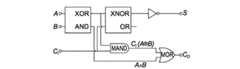
<全加算器の実施の形態>
アーキテクチャの多機能性(則ち、単一ゲートにおける1つ以上の論理演算出力)は、より複雑な回路のコンパクトな設計を提供する。これは、全加算回路設計において証明される。図5は、アンバッファ(弱)XOR−XOR 2T−10M全加算器設計を示す。これは、各々が図3の回路に相当する2つの多機能論理ゲート30を含んでいる。加算されるべき2ビットが、入力部A,Bに印加され、入力キャリービットが端子Ciに印加される。総数ビットが、出力端子Sに現れ、出力キャリービットが端子Coに現れる。<Embodiment of Full Adder>
The versatility of the architecture (ie, one or more logical operations output in a single gate) provides a compact design of more complex circuits. This is demonstrated in full adder circuit design. FIG. 5 shows an unbuffered (weak) XOR-XOR 2T-10M full adder design. It includes two
バッファタイプ及びアンバッファの全加算器の選択が設計された。これらの構造の説明を簡単にするために、図6から8を参照する。図6は、ORゲートを形成するために接続された2つのメモリスタを示す。このORゲートは、メモリスタORゲート、又はMORゲートと呼ばれ、対応する記号を図面の右手側に示す。図7は、ANDゲートを形成するために接続された2つのメモリスタを示す。このANDゲートは、メモリスタANDゲート、又はMANDゲートと呼ばれ、対応する記号を図面の右手側に示す。図8は、インバータ(NOTゲート)を形成するために接続された2つのトランジスタを示す。このインバータは、反転バッファとして動作し、対応する記号を図面の右手側に示す。 Selection of buffer type and unbuffered full adders was designed. To simplify the description of these structures, reference is made to FIGS. FIG. 6 shows two memristors connected to form an OR gate. This OR gate is called a memristor OR gate or a MOR gate and the corresponding symbols are shown on the right hand side of the figure. FIG. 7 shows two memristors connected to form an AND gate. This AND gate is called a memristor AND gate or a MAND gate and the corresponding symbols are shown on the right hand side of the figure. FIG. 8 shows two transistors connected to form an inverter (NOT gate). This inverter acts as an inverting buffer and the corresponding symbols are shown on the right hand side of the figure.
構造を表2に示す。「アーキテクチャ」の欄は、第1及び第2総和ステージにおける図3及び4のアーキテクチャを使用する可能な方法の全てを示す。「アンバッファ」及び「バッファタイプ」の欄は、アンバッファ及びバッファタイプ全加算器に対し、使用されるトランジスタ及びメモリスタ素子の個数と、必要とされる素子(構成要素)の全体数とをまとめている。対応する回路をアンバッファ用に図9aーdに示し、バッファタイプ用に図10a−d(a−dは、表2に示すアーキテクチャの列1−4に相当)に示す。図9及び10において、XOR及びANDとラベルが付された出力部を有するボックスは、図3の回路であり、OR及びXNORとラベルが付された出力部を有するボックスは、図4の回路である。他の記号は、図6から8の回路に相当する。図9aの回路は、図5の回路と同じであるが、メモリスタM5、M6がMORゲート記号に置換されている。The structure is shown in Table 2. The "Architecture" column shows all of the possible ways of using the architectures of FIGS. 3 and 4 in the first and second summing stages. The "Unbuffered" and "Buffered" columns summarize the number of transistors and memristor elements used and the total number of required elements (components) for unbuffered and buffered type full adders. ing. The corresponding circuits are shown in FIGS. 9 a-d for unbuffering and in FIGS. 10 a-d for buffer types (ad corresponding to columns 1-4 of the architecture shown in Table 2). 9 and 10, the box with the outputs labeled XOR and AND is the circuit of FIG. 3 and the box with the outputs labeled OR and XNOR is the circuit of FIG. is there. Other symbols correspond to the circuits of FIGS. The circuit of FIG. 9a is the same as the circuit of FIG. 5, but memristors M5 and M6 are replaced by MOR gate symbols.
表2において、「バッファタイプ」の欄は、CMOSインバータを備え、出力部(図10に示す回路)でスイングする全電圧を達成する構成を表す。この欄において、XOR−XOR構成は、最もコンパクトであり(10T−12M)、高い信頼性性能を示す。この回路を図10aに示す。分かるように、CMOSインバータは、各XOR出力部に接続され、キャリーは二重に反転される。ここで、これは、3T+3T+4T=10T、且つ8M+2M+2M=12Mを必要とする。これは、既存の構成、例えば16T−18M及び27T−2Mを使う構成よりも実質的に優れている。 In Table 2, the "buffer type" column represents a configuration that includes a CMOS inverter to achieve a full voltage swing at the output (the circuit shown in FIG. 10). In this column, the XOR-XOR configuration is the most compact (10T-12M) and exhibits high reliability performance. This circuit is shown in FIG. 10a. As can be seen, a CMOS inverter is connected to each XOR output and the carry is double inverted. Here, this requires 3T + 3T + 4T = 10T, and 8M + 2M + 2M = 12M. This is substantially superior to existing configurations, such as those using 16T-18M and 27T-2M.
<性能>
メモリスタは、VTEAMモデルに基づいたVerilog-Aにコード化され(Kvatinsky, S., Ramadan, M., Friedman, E. G., Kolodny, A.: 'VTEAM: A General Model for Voltage-Controlled Memristors', IEEE Trans. Circuits Syst. II: Express briefs, 2015, 62, (8), PP. 786-790)、回路は、Cadence Virtuoso(登録商標)において設計されてシミュレートされた。
また、これは、RONに亘って約0.24Vの降下を保証して、設計ルール(2)を満足する。ROFFが高くなるにつれて、例えばROFF=80KΩの場合、電力性能もより良くなる。<Performance>
Memista is encoded in Verilog-A based on VTEAM model (Kvantsky, S., Ramadan, M., Friedman, EG, Kolodny, A .: 'VTEAM: A General Model for Voltage-Controlled Memristors', IEEE Trans Circuits Syst. II: Express briefs, 2015, 62, (8), PP. 786-790), circuits were designed and simulated in Cadence Virtuoso®.
Also, this guarantees a drop of approximately 0.24 V across RON , satisfying design rule (2). As ROFF increases, for example, when ROFF = 80 KΩ, the power performance also improves.
本発明の3T−4Mの実施の形態の性能を、Mishra等からのCMOSベース構成と比較した(Mishra, S. S., Agrawal, A. K., Nagaria, R. K.: 'A comparative performance analysis of various CMOS design techniques for XOR and XNOR circuits', International Journal on Emerging Technologies, 2010, 1, (1), pp. 1-10)。表3の最初の2つの列は、3T−4M XOR及びXNORゲート(それぞれ図4及び3に相当し、XNOR又はXORの出力部において図8のさらなる2Tインバータ・バッファを備える)の性能を表す。一方、最後の2つの列は、Mishra等の10T/8T CMOS XOR/XNORゲートの性能を表す。後者の構成は、「弱」6T XORゲートに基づいている。負荷容量は、1フェムトファラッド(fF)になると考えられた。電力(単位はマイクロワット(μW))は、全静的及びダイナミック電力の平均である。本発明の実施の形態による両構成は、一貫した性能を8GHzに維持しながらも、必要とされる電力がCMOS構成よりもかなり少なくなる。実際、CMOS構成は、4GHz周波数近傍で機能しなくなった(正しい動作を示す「Stat」又はステータス欄:通過又は失敗)。さらに、バッファタイプXNOR構成の実施の形態は、バッファタイプXOR構成の実施の携帯よりも相当電力効率が良い。これは、NMOST対PMOSTの使用によるところであり、これらは、図3及び4に示すように接続されている。 The performance of the 3T-4M embodiment of the present invention was compared to the CMOS-based configuration from Mishra et al. (Mishra, SS, Agrawal, AK, Nagaria, RK: 'A comparative performance analysis of various CMOS design techniques for XOR and XNOR circuits', International Journal on Emerging Technologies, 2010, 1, (1), pp. 1-10). The first two columns of Table 3 represent the performance of 3T-4M XOR and XNOR gates (corresponding to FIGS. 4 and 3 respectively, with the additional 2T inverter buffer of FIG. 8 at the output of XNOR or XOR). The last two columns, on the other hand, represent the performance of a 10T / 8T CMOS XOR / XNOR gate such as Mishra et al. The latter configuration is based on a "weak" 6T XOR gate. The loading capacity was considered to be 1 femtofarad (fF). Power (in microwatts (μW)) is the average of all static and dynamic power. Both configurations according to embodiments of the present invention require much less power than CMOS configurations while maintaining consistent performance at 8 GHz. In fact, the CMOS configuration has failed near the 4 GHz frequency ("Stat" or status column indicating correct operation: pass or fail). Furthermore, embodiments of the buffer type XNOR configuration are significantly more power efficient than the mobile implementation of the buffer type XOR configuration. This is due to the use of NMOST vs. PMOST, which are connected as shown in FIGS.
図11は、周知の構成と比較した、8GHzでの上記3T−4MバッファタイプXORゲート実施の形態の性能を示す。上部の2つの信号は、端子A及びBに印加される入力電圧であり、3番目のグラフは、Mishra等の10T CMOS XORゲートの出力である。4番目のグラフは、Mathew等からの6T−2Mハイブリッド・メモリスタCMOSベースのXOR構成の出力である(Mathew, J., Chakraborty, R. S., Sahoo, D. P., Yang, Y., Pradhan, D.K.: 'A novel memristor based physically uncloneable function', ELSEVIER, INTEGRATION, the VLSI journal, 2015 51, pp. 37-45)。最下段のグラフは、3T−4MバッファタイプXORゲートの実施の形態の出力である。不適切な論理演算や不完全な電圧スイングによって分かるように、比較例の10TCMOS及び6T−2M XORゲートは、機能しない。 FIG. 11 shows the performance of the above 3T-4M buffer type XOR gate implementation at 8 GHz compared to the known configuration. The top two signals are the input voltage applied to terminals A and B, and the third graph is the output of a 10T CMOS XOR gate such as Mishra et al. The fourth graph is the output of the 6T-2M hybrid Memorista CMOS-based XOR configuration from Mathew et al. (Mathew, J., Chakraborty, RS, Sahoo, DP, Yang, Y., Pradhan, DK: 'A: novel memristor based physically uncloneable function ', ELSEVIER, INTEGRATION, the VLSI journal, 2015, 51, pp. 37-45). The bottom graph is the output of the 3T-4M buffer type XOR gate embodiment. The comparative 10 TCMOS and 6T-2M XOR gates do not work, as evidenced by improper logic operations and incomplete voltage swings.
表2におけるバッファタイプ全加算器構成も、様々な周波数でテストされた。最初の列からの10T−12M構成(XOR−XORアーキテクチャ)は、8GHzで正確に動作し、63.53μWの電力を必要とした。これは、単一のCMOS XORゲートによって消費される電力よりも低い(表3)。 The buffer type full adder configuration in Table 2 was also tested at various frequencies. The 10T-12M configuration (XOR-XOR architecture) from the first column worked correctly at 8 GHz and required 63.53 μW of power. This is lower than the power consumed by a single CMOS XOR gate (Table 3).
<さらなる変形例>
図2を参照すると、メモリスタM2,M4は、入力部A,BについてのORゲートを形成し、このORは、出力部12に現れる電圧VL1になる(図6の「MOR」ゲートを参照)。メモリスタM1,M3は、入力部A,BについてのANDゲートを形成し、このANDは、出力部14に現れる電圧VL2になる(図7の「MAND」ゲートを参照)。図2の純メモリスタアーキテクチャは、XORゲートのように動作する(表1)。ここで、NMOS及びPMOSトランジスタが、適切に動作し、且つXOR及びXNORゲート機能を提供するためには、VL1>=VL2である(図3及び4)。<Further modification>
With reference to FIG. 2, the memristor M2 , M4 form an OR gate for the inputs A, B, which becomes the voltage VL1 appearing at the output 12 (see the “MOR” gate of FIG. reference). The memristor M1 , M3 form an AND gate for the inputs A, B, which will be the voltage VL2 appearing at the output 14 (see “MAND” gate in FIG. 7). The pure memristor architecture of FIG. 2 acts like an XOR gate (Table 1). Here, in order for the NMOS and PMOS transistors to operate properly and provide XOR and XNOR gate functions, VL1 > = VL2 (FIGS. 3 and 4).
図12の回路60に示されるように、メモリスタの極性を反転させることも可能である。出力部62での電圧VL1は、入力部A,BでのAND演算であり、出力部64での電圧VL2は、OR演算であり、則ち、AND及びORゲートが図2に比較してスワッピングされる。この場合、回路は、純メモリスタXNOR機能のように動作する。しかしながら、この場合、トランジスタTが動作してXOR及びXNOR機能を提供するためには、VL2>=VL1を保証する必要がある(図13及び14をそれぞれ参照)。VL1及びVL2の役割は、図3及び4に比較して、図13及び14において逆になることに留意する(端子12,14及び端子64,62を参照)。これらの変化によって、図13の回路は、図3の回路と同じであり、図14の回路は、図4の回路と同じである。As shown in
高性能多機能論理アーキテクチャが現れ、既存のCMOS技術とシームレスに統合されうる。一の実施の形態は、1つのトランジスタ及び4つのメモリスタ(1T−4M)からなる構成であり、この構成は、既存の技術に比較して、必要とされるトランジスタ及びメモリスタの数がかなり少ない。発明を具体化する構成は、特に高周波数でのチップ面積、電力消費、及び信頼性能の観点から、ハイブリッドCMOSメモリスタ構成と同様に、既存のCMOSよりも格段に優れている。 A high performance multifunction logic architecture emerges and can be seamlessly integrated with existing CMOS technology. One embodiment is a configuration consisting of one transistor and four memristor (1T-4M), which requires significantly less number of transistors and memristor compared to existing technologies. Configurations embodying the invention are significantly superior to existing CMOS, as well as hybrid CMOS memristor configurations, particularly in terms of chip area at high frequency, power consumption, and reliability performance.
特に、1T−4M構成は、単一の周期において、則ち入力が印加される同一周期の間に、複数機能(XOR/AND又はXNOR/OR)を実現し、既存の技術に比較して、オーバーヘッドの最も少ない状態で、既存のCMOS技術にシームレスに統合される。メモリスタの1つの長所は、メモリスタを3Dに組むことができることであり、一方、CMOSでは、2Dの組み立てのみが可能である。これによって、メモリスタは、Z軸に沿って組み立て、CMOSレイアウトのX−Y軸に亘って層をなすように配置されることが可能になる。さらに、CMOSの容量は、CMOSベースシステムのかなり乏しい上方限界をより高周波数に設定する阻害要因である。CMOSベース構成のこれらの短所は、本発明の実施の形態においてCMOSトランジスタの個数を減らすことによってアドレスされる。これは、高周波数での実施の形態の信頼性をかなり改善するのみならず、電力消費をかなり減らして、チップ面積利用をより良いものとする。後者は、空間がCMOS層内に解放されるので可能になる。このCMOS層内では、CMOS機能が、CMOS技術のみに依存したユニットによって組み込まれる。提案された実施の形態は、メモリスタカウントの減少も可能にする。 In particular, the 1T-4M configuration implements multiple functions (XOR / AND or XNOR / OR) in a single period, ie during the same period when the input is applied, compared to existing techniques, Seamlessly integrated into existing CMOS technology with minimal overhead. One advantage of memristor is that it can be assembled in 3D, while in CMOS only 2D assembly is possible. This allows the memristor to be assembled along the Z-axis and arranged to be layered across the XY layout of the CMOS layout. Furthermore, CMOS capacitance is a limiting factor that sets the rather poor upper bound of CMOS based systems to higher frequencies. These shortcomings of CMOS based configurations are addressed by reducing the number of CMOS transistors in embodiments of the present invention. This not only significantly improves the reliability of the high frequency embodiment but also significantly reduces power consumption and makes chip area utilization better. The latter is possible because space is released into the CMOS layer. Within this CMOS layer, the CMOS functionality is incorporated by a unit dependent only on CMOS technology. The proposed embodiment also enables the reduction of memristor counts.
さらに、本発明を具体化するアーキテクチャの多機能性の特徴によって、本明細書で定義される、最適化・低複雑度・全加算回路によって証明されるような、コンパクト且つ効率的なシステムの設計が可能になる。 Furthermore, the compact and efficient design of the system as evidenced by the optimization, low complexity, full adder circuit defined herein by the multifunctional features of the architecture embodying the invention. Becomes possible.
M1、M2、M3、M4 メモリスタ
A、B 入力部
12,14 出力部M1 , M2 , M3 , M4 memristor A,
Claims (11)
Translated fromJapanese各が正極端子及び負極端子を有する第1メモリスタ、第2メモリスタ、第3メモリスタ及び第4メモリスタと、
第1出力部及び第2出力部と、
を備え、
前記第1メモリスタの負極端子と前記第2メモリスタの正極端子とは、前記第1入力部に共通に接続され、
前記第3メモリスタの負極端子と前記第4メモリスタの正極端子とは、前記第2入力部に共通に接続され、
前記第2メモリスタの負極端子と前記第4メモリスタの負極端子とは、前記第1出力部に共通に接続され、
前記第1メモリスタの正極端子と前記第3メモリスタの正極端子とは、前記第2出力部に共通に接続され、
使用するときは、前記出力部の少なくとも一方の電圧、則ち、前記第1及び第2出力部間の電位差は、前記第1及び第2入力部に印加された電圧に対する論理演算の結果に相当する、論理ゲート。A first input unit and a second input unit;
A first memristor, a second memristor, a third memristor and a fourth memristor, each having a positive terminal and a negative terminal;
A first output unit and a second output unit;
Equipped with
The negative terminal of the first memristor and the positive terminal of the second memristor are commonly connected to the first input unit,
The negative terminal of the third memristor and the positive terminal of the fourth memristor are commonly connected to the second input unit,
The negative terminal of the second memristor and the negative terminal of the fourth memristor are commonly connected to the first output unit,
The positive terminal of the first memristor and the positive terminal of the third memristor are commonly connected to the second output unit,
When used, the voltage of at least one of the outputs, ie, the potential difference between the first and second outputs, corresponds to the result of a logical operation on the voltage applied to the first and second inputs. To be a logic gate.
前記トランジスタのゲートは、前記第1及び第2出力部の一方に接続され、
前記トランジスタのドレインは、前記第1及び第2出力部の他方に接続され、
前記トランジスタのソースは、正又は負の供給電圧に接続されるか、又は接地される、請求項1又は2に記載の論理ゲート。Further comprising a transistor,
The gate of the transistor is connected to one of the first and second output parts,
The drain of the transistor is connected to the other of the first and second outputs.
A logic gate according to claim 1 or 2, wherein the source of the transistor is connected to the positive or negative supply voltage or is grounded.
前記インバータの入力部は、前記第1及び第2出力部の一方に接続されて、バッファタイプの出力を前記インバータの出力部に提供する、請求項1から7のいずれか一に記載の論理ゲート。Equipped with at least one inverter,
8. A logic gate as claimed in any one of the preceding claims, wherein the input of the inverter is connected to one of the first and second outputs to provide a buffer type output at the output of the inverter. .
11. The full adder circuit of claim 10, further comprising at least two additional memristors configured to provide at least one of an OR gate and an AND gate.
Applications Claiming Priority (3)
| Application Number | Priority Date | Filing Date | Title |
|---|---|---|---|
| GB1603089.2 | 2016-02-23 | ||
| GB1603089.2AGB2548081B (en) | 2016-02-23 | 2016-02-23 | Logic gate |
| PCT/GB2017/050431WO2017144862A1 (en) | 2016-02-23 | 2017-02-20 | Memristor based logic gate |
Publications (2)
| Publication Number | Publication Date |
|---|---|
| JP2019512196Atrue JP2019512196A (en) | 2019-05-09 |
| JP6888029B2 JP6888029B2 (en) | 2021-06-16 |
Family
ID=55753025
Family Applications (1)
| Application Number | Title | Priority Date | Filing Date |
|---|---|---|---|
| JP2018562725AActiveJP6888029B2 (en) | 2016-02-23 | 2017-02-20 | Memory star-based logic gate |
Country Status (6)
| Country | Link |
|---|---|
| US (1) | US10860291B2 (en) |
| EP (1) | EP3420556B1 (en) |
| JP (1) | JP6888029B2 (en) |
| KR (1) | KR102704612B1 (en) |
| GB (1) | GB2548081B (en) |
| WO (1) | WO2017144862A1 (en) |
Cited By (1)
| Publication number | Priority date | Publication date | Assignee | Title |
|---|---|---|---|---|
| JP7546948B2 (en) | 2019-10-02 | 2024-09-09 | オックスフォード ブルックス ユニバーシティ | Sensors |
Families Citing this family (30)
| Publication number | Priority date | Publication date | Assignee | Title |
|---|---|---|---|---|
| US10516398B2 (en)* | 2016-05-24 | 2019-12-24 | Technion Research & Development Foundation Limited | Logic design with unipolar memristors |
| US10171083B2 (en) | 2016-12-05 | 2019-01-01 | Board Of Regents, The University Of Texas System | Memristor logic design using driver circuitry |
| WO2018193338A1 (en)* | 2017-04-20 | 2018-10-25 | King Abdullah University Of Science And Technology | Stochastic memristor logic devices |
| GB201708512D0 (en) | 2017-05-26 | 2017-07-12 | Univ Southampton | Tunable cmos circuit, template matching module, neural spike recording system, and fuzzy logic gate |
| US9921808B1 (en)* | 2017-06-02 | 2018-03-20 | Board Of Regents, The University Of Texas System | Memristor-based adders using memristors-as-drivers (MAD) gates |
| CN109308920B (en)* | 2017-07-27 | 2020-11-13 | 中芯国际集成电路制造(上海)有限公司 | Power supply control circuit for static random access memory array |
| US10305484B2 (en) | 2017-09-08 | 2019-05-28 | Board Of Regents, The University Of Texas System | Memristor-based dividers using memristors-as-drivers (MAD) gates |
| US10706923B2 (en) | 2017-09-08 | 2020-07-07 | Arizona Board Of Regents On Behalf Of Arizona State University | Resistive random-access memory for exclusive NOR (XNOR) neural networks |
| US10318242B2 (en) | 2017-09-08 | 2019-06-11 | Board Of Regents, The University Of Texas System | Memristor-based multipliers using memristors-as-drivers (MAD) gates |
| CN108449080B (en)* | 2018-04-20 | 2020-06-05 | 西南大学 | A full-add circuit based on CMOS inverters and memristors |
| CN109032561B (en)* | 2018-07-20 | 2022-10-14 | 福州大学 | Reversible logic adder circuit with carry bypass output as carry selection |
| CN110634516B (en)* | 2018-11-16 | 2021-10-01 | 中山大学 | Programmable Multifunction Spin Logic Adder/Subtracter |
| KR102156357B1 (en)* | 2018-12-17 | 2020-09-15 | 연세대학교 산학협력단 | Image acquisition system and method for acquiring a uniform interval image using an swipe line imaging sensor, and fingerprint authentication system and controller system including the same |
| CN110690891B (en)* | 2019-09-26 | 2021-03-02 | 郑州轻工业学院 | Four-input-four-output multifunctional encoder circuit based on memristor |
| CN111046617B (en)* | 2019-12-23 | 2024-04-09 | 杭州电子科技大学 | Memristor-based three-value digital logic gate circuit |
| DE102020206792A1 (en) | 2020-05-29 | 2021-12-02 | Fraunhofer-Gesellschaft zur Förderung der angewandten Forschung eingetragener Verein | Device and method for generating hardware-based, physically non-clonable functions and their use |
| DE102020206790A1 (en) | 2020-05-29 | 2021-12-02 | Fraunhofer-Gesellschaft zur Förderung der angewandten Forschung eingetragener Verein | Device and method for hardware-based generation of random numbers and number sequences |
| US11653578B2 (en)* | 2020-12-01 | 2023-05-16 | International Business Machines Corporation | Phase-change material-based XOR logic gates |
| CN112910457B (en)* | 2021-01-21 | 2023-04-14 | 西南大学 | A memristor-based data selector and its IC topology |
| CN113285705B (en)* | 2021-04-26 | 2022-05-17 | 杭州电子科技大学 | Mixed CMOS-memristor full adder circuit |
| KR102521515B1 (en)* | 2021-05-24 | 2023-04-13 | 경북대학교 산학협력단 | Design method of the ternary logic using memristors and mosfets, recording medium and device for performing the method |
| CN113362872B (en)* | 2021-06-16 | 2022-04-01 | 华中科技大学 | Memristor-based complete nonvolatile Boolean logic circuit and operation method |
| CN113872589B (en)* | 2021-09-03 | 2025-04-25 | 杭州电子科技大学 | Balanced three-value multiplexer circuit based on memristor |
| KR102656337B1 (en)* | 2021-11-26 | 2024-04-11 | 경희대학교 산학협력단 | Semiconductor device based on ternary precision xnor logic and neuromorphic computing system including the same |
| CN114244349B (en)* | 2021-12-06 | 2025-04-29 | 国网辽宁省电力有限公司信息通信分公司 | A one-bit binary adder circuit based on memristor |
| CN114741050B (en)* | 2022-04-11 | 2024-07-26 | 安徽工程大学 | Full adder circuit, high carry circuit and adder based on memristor and CMOS transistor |
| US20230421156A1 (en)* | 2022-06-24 | 2023-12-28 | Qualcomm Incorporated | Glitch absorbing buffer for digital circuits |
| CN116488636A (en)* | 2023-04-25 | 2023-07-25 | 南京邮电大学 | Universal logic circuit based on memristor design |
| US12345757B2 (en)* | 2023-05-01 | 2025-07-01 | Mellanox Technologies, Ltd | Decoupling cells testability |
| CN117595859B (en)* | 2024-01-19 | 2024-05-14 | 山东云海国创云计算装备产业创新中心有限公司 | A logic circuit, output method and electronic device based on memristor |
Family Cites Families (17)
| Publication number | Priority date | Publication date | Assignee | Title |
|---|---|---|---|---|
| JPH05152936A (en) | 1991-11-29 | 1993-06-18 | Oki Electric Ind Co Ltd | Logic circuit |
| US5859548A (en)* | 1996-07-24 | 1999-01-12 | Lg Semicon Co., Ltd. | Charge recycling differential logic (CRDL) circuit and devices using the same |
| EP1752871A1 (en)* | 2005-07-20 | 2007-02-14 | STMicroelectronics (Research & Development) Limited | Multiplier with speed optimised carry save adder tree |
| JP5388525B2 (en)* | 2008-09-25 | 2014-01-15 | 株式会社東芝 | Programmable logic circuit |
| WO2010068221A1 (en)* | 2008-12-12 | 2010-06-17 | Hewlett-Packard Development Company, L.P. | Memristive device |
| US8274312B2 (en)* | 2011-02-25 | 2012-09-25 | The United States Of America As Represented By The Secretary Of The Air Force | Self-reconfigurable memristor-based analog resonant computer |
| EP2815478B1 (en)* | 2012-02-15 | 2017-03-22 | Qualcomm Incorporated | Surge protection for differential input/output interfaces |
| CN102811051B (en)* | 2012-07-09 | 2014-10-29 | 华中科技大学 | A logic gate circuit based on memristor |
| US8773167B2 (en)* | 2012-07-30 | 2014-07-08 | Hewlett-Packard Development Company, L.P. | Implementing logic circuits with memristors |
| TWI469325B (en)* | 2012-07-31 | 2015-01-11 | Ind Tech Res Inst | Logic gate |
| US9412940B2 (en)* | 2012-08-03 | 2016-08-09 | Ecole Polytechnique Federale De Lausanne (Epfl) | Resistive switching element and use thereof |
| KR20140071556A (en)* | 2012-11-26 | 2014-06-12 | 전북대학교산학협력단 | Memristor bridge circuit, and memristive bridge synapse circuit and neuron circuit using the same |
| FR3001571B1 (en)* | 2013-01-30 | 2016-11-25 | Commissariat Energie Atomique | METHOD FOR PROGRAMMING A MEMORY DEVICE WITH BIPOLAR SWITCHING |
| US20150019468A1 (en)* | 2013-07-09 | 2015-01-15 | Knowmtech, Llc | Thermodynamic computing |
| US9299917B2 (en)* | 2013-09-30 | 2016-03-29 | Northwestern University | Magnetic tunnel junctions with control wire |
| US9685954B2 (en)* | 2014-03-09 | 2017-06-20 | Technion Research & Development Foundation Ltd. | Pure memristive logic gate |
| CN104124960B (en) | 2014-06-20 | 2018-02-23 | 华中科技大学 | A kind of non-volatile boolean calculation circuit and its operating method |
- 2016
- 2016-02-23GBGB1603089.2Apatent/GB2548081B/ennot_activeExpired - Fee Related
- 2017
- 2017-02-20KRKR1020187027383Apatent/KR102704612B1/enactiveActive
- 2017-02-20JPJP2018562725Apatent/JP6888029B2/enactiveActive
- 2017-02-20USUS16/079,160patent/US10860291B2/enactiveActive
- 2017-02-20WOPCT/GB2017/050431patent/WO2017144862A1/ennot_activeCeased
- 2017-02-20EPEP17706875.6Apatent/EP3420556B1/enactiveActive
Cited By (1)
| Publication number | Priority date | Publication date | Assignee | Title |
|---|---|---|---|---|
| JP7546948B2 (en) | 2019-10-02 | 2024-09-09 | オックスフォード ブルックス ユニバーシティ | Sensors |
Also Published As
| Publication number | Publication date |
|---|---|
| JP6888029B2 (en) | 2021-06-16 |
| KR20180115773A (en) | 2018-10-23 |
| KR102704612B1 (en) | 2024-09-06 |
| EP3420556A1 (en) | 2019-01-02 |
| GB201603089D0 (en) | 2016-04-06 |
| GB2548081A (en) | 2017-09-13 |
| GB2548081B (en) | 2019-10-02 |
| EP3420556B1 (en) | 2020-04-08 |
| US20190056915A1 (en) | 2019-02-21 |
| WO2017144862A1 (en) | 2017-08-31 |
| US10860291B2 (en) | 2020-12-08 |
Similar Documents
| Publication | Publication Date | Title |
|---|---|---|
| JP6888029B2 (en) | Memory star-based logic gate | |
| Wang et al. | High-density memristor-CMOS ternary logic family | |
| Zanotti et al. | Smart logic-in-memory architecture for low-power non-von neumann computing | |
| Balatti et al. | Normally-off logic based on resistive switches—Part I: Logic gates | |
| CN1333528C (en) | Reconfigurable logical circuit using transistor having spin-dependent transmission characteristics | |
| CN106941350B (en) | A memristor-based XOR gate circuit and design and fabrication method | |
| CN105739944A (en) | Multi-system additive operation circuit based on memristors and operation method thereof | |
| CN105356876B (en) | Memristor-Based Logic Gates | |
| CN103051307B (en) | Memristor-based non-volatile D trigger | |
| Teimoori et al. | A novel hybrid CMOS-memristor logic circuit using Memristor Ratioed Logic | |
| WO2012108151A1 (en) | Nonvolatile latch circuit, nonvolatile flip-flop circuit and nonvolatile signal processing device | |
| WO2023155439A1 (en) | Electronic device and memristor-based logic gate circuit thereof | |
| US8324932B2 (en) | High-speed static XOR circuit | |
| Puglisi et al. | SIMPLY: Design of a RRAM-based smart logic-in-memory architecture using RRAM compact model | |
| US8218714B2 (en) | Neuron MOS transistor based multi-digit multi-valued counter | |
| JPH01216622A (en) | Logic circuit | |
| CN105869672B (en) | A kind of non-volatile FPGA programming dot circuits and its operating method based on RRAM | |
| WO2018105719A1 (en) | Reading device and logic device | |
| Yang et al. | Novel memristive logic architectures | |
| JP6291947B2 (en) | Drive circuit, integrated circuit device, and charge pump circuit control method | |
| Mozafari et al. | A Novel Architecture for Memristor-Based Logic | |
| WO2018207831A1 (en) | Programmable logic circuit and semiconductor device using same | |
| CN105210297A (en) | Circuit implementing xor operation, circuit implementing xnor operation, and array circuit | |
| JP4097912B2 (en) | NOT circuit and electronic circuit using the same | |
| Zain et al. | Simulation study of memristor aided logic (MAGIC) based on CMOS NOR gate |
Legal Events
| Date | Code | Title | Description |
|---|---|---|---|
| A621 | Written request for application examination | Free format text:JAPANESE INTERMEDIATE CODE: A621 Effective date:20200114 | |
| A977 | Report on retrieval | Free format text:JAPANESE INTERMEDIATE CODE: A971007 Effective date:20200819 | |
| A131 | Notification of reasons for refusal | Free format text:JAPANESE INTERMEDIATE CODE: A131 Effective date:20200825 | |
| A601 | Written request for extension of time | Free format text:JAPANESE INTERMEDIATE CODE: A601 Effective date:20201120 | |
| A521 | Request for written amendment filed | Free format text:JAPANESE INTERMEDIATE CODE: A523 Effective date:20210122 | |
| TRDD | Decision of grant or rejection written | ||
| A01 | Written decision to grant a patent or to grant a registration (utility model) | Free format text:JAPANESE INTERMEDIATE CODE: A01 Effective date:20210420 | |
| A61 | First payment of annual fees (during grant procedure) | Free format text:JAPANESE INTERMEDIATE CODE: A61 Effective date:20210519 | |
| R150 | Certificate of patent or registration of utility model | Ref document number:6888029 Country of ref document:JP Free format text:JAPANESE INTERMEDIATE CODE: R150 | |
| R250 | Receipt of annual fees | Free format text:JAPANESE INTERMEDIATE CODE: R250 | |
| R250 | Receipt of annual fees | Free format text:JAPANESE INTERMEDIATE CODE: R250 |