JP2019211508A - Semiconductor module, method for manufacturing the same, and method for communication using the same - Google Patents
Semiconductor module, method for manufacturing the same, and method for communication using the sameDownload PDFInfo
- Publication number
- JP2019211508A JP2019211508AJP2018104842AJP2018104842AJP2019211508AJP 2019211508 AJP2019211508 AJP 2019211508AJP 2018104842 AJP2018104842 AJP 2018104842AJP 2018104842 AJP2018104842 AJP 2018104842AJP 2019211508 AJP2019211508 AJP 2019211508A
- Authority
- JP
- Japan
- Prior art keywords
- semiconductor
- semiconductor chip
- wiring
- semiconductor module
- insulating film
- Prior art date
- Legal status (The legal status is an assumption and is not a legal conclusion. Google has not performed a legal analysis and makes no representation as to the accuracy of the status listed.)
- Granted
Links
Images


Classifications
- H—ELECTRICITY
- H04—ELECTRIC COMMUNICATION TECHNIQUE
- H04B—TRANSMISSION
- H04B10/00—Transmission systems employing electromagnetic waves other than radio-waves, e.g. infrared, visible or ultraviolet light, or employing corpuscular radiation, e.g. quantum communication
- H04B10/80—Optical aspects relating to the use of optical transmission for specific applications, not provided for in groups H04B10/03 - H04B10/70, e.g. optical power feeding or optical transmission through water
- G—PHYSICS
- G02—OPTICS
- G02B—OPTICAL ELEMENTS, SYSTEMS OR APPARATUS
- G02B6/00—Light guides; Structural details of arrangements comprising light guides and other optical elements, e.g. couplings
- G02B6/10—Light guides; Structural details of arrangements comprising light guides and other optical elements, e.g. couplings of the optical waveguide type
- G02B6/12—Light guides; Structural details of arrangements comprising light guides and other optical elements, e.g. couplings of the optical waveguide type of the integrated circuit kind
- G02B6/12004—Combinations of two or more optical elements
- G—PHYSICS
- G02—OPTICS
- G02B—OPTICAL ELEMENTS, SYSTEMS OR APPARATUS
- G02B6/00—Light guides; Structural details of arrangements comprising light guides and other optical elements, e.g. couplings
- G02B6/24—Coupling light guides
- G02B6/42—Coupling light guides with opto-electronic elements
- G02B6/4201—Packages, e.g. shape, construction, internal or external details
- G02B6/4274—Electrical aspects
- H—ELECTRICITY
- H01—ELECTRIC ELEMENTS
- H01L—SEMICONDUCTOR DEVICES NOT COVERED BY CLASS H10
- H01L24/00—Arrangements for connecting or disconnecting semiconductor or solid-state bodies; Methods or apparatus related thereto
- H01L24/91—Methods for connecting semiconductor or solid state bodies including different methods provided for in two or more of groups H01L24/80 - H01L24/90
- H01L24/92—Specific sequence of method steps
- H—ELECTRICITY
- H01—ELECTRIC ELEMENTS
- H01L—SEMICONDUCTOR DEVICES NOT COVERED BY CLASS H10
- H01L25/00—Assemblies consisting of a plurality of semiconductor or other solid state devices
- H01L25/16—Assemblies consisting of a plurality of semiconductor or other solid state devices the devices being of types provided for in two or more different subclasses of H10B, H10D, H10F, H10H, H10K or H10N, e.g. forming hybrid circuits
- H01L25/167—Assemblies consisting of a plurality of semiconductor or other solid state devices the devices being of types provided for in two or more different subclasses of H10B, H10D, H10F, H10H, H10K or H10N, e.g. forming hybrid circuits comprising optoelectronic devices, e.g. LED, photodiodes
- G—PHYSICS
- G02—OPTICS
- G02B—OPTICAL ELEMENTS, SYSTEMS OR APPARATUS
- G02B6/00—Light guides; Structural details of arrangements comprising light guides and other optical elements, e.g. couplings
- G02B6/10—Light guides; Structural details of arrangements comprising light guides and other optical elements, e.g. couplings of the optical waveguide type
- G02B6/12—Light guides; Structural details of arrangements comprising light guides and other optical elements, e.g. couplings of the optical waveguide type of the integrated circuit kind
- G02B2006/12083—Constructional arrangements
- G02B2006/12107—Grating
- G—PHYSICS
- G02—OPTICS
- G02B—OPTICAL ELEMENTS, SYSTEMS OR APPARATUS
- G02B6/00—Light guides; Structural details of arrangements comprising light guides and other optical elements, e.g. couplings
- G02B6/24—Coupling light guides
- G02B6/26—Optical coupling means
- G02B6/30—Optical coupling means for use between fibre and thin-film device
- G02B6/305—Optical coupling means for use between fibre and thin-film device and having an integrated mode-size expanding section, e.g. tapered waveguide
- G—PHYSICS
- G02—OPTICS
- G02B—OPTICAL ELEMENTS, SYSTEMS OR APPARATUS
- G02B6/00—Light guides; Structural details of arrangements comprising light guides and other optical elements, e.g. couplings
- G02B6/24—Coupling light guides
- G02B6/42—Coupling light guides with opto-electronic elements
- G—PHYSICS
- G02—OPTICS
- G02B—OPTICAL ELEMENTS, SYSTEMS OR APPARATUS
- G02B6/00—Light guides; Structural details of arrangements comprising light guides and other optical elements, e.g. couplings
- G02B6/24—Coupling light guides
- G02B6/42—Coupling light guides with opto-electronic elements
- G02B6/4201—Packages, e.g. shape, construction, internal or external details
- G02B6/4204—Packages, e.g. shape, construction, internal or external details the coupling comprising intermediate optical elements, e.g. lenses, holograms
- G02B6/4206—Optical features
- H—ELECTRICITY
- H01—ELECTRIC ELEMENTS
- H01L—SEMICONDUCTOR DEVICES NOT COVERED BY CLASS H10
- H01L2224/00—Indexing scheme for arrangements for connecting or disconnecting semiconductor or solid-state bodies and methods related thereto as covered by H01L24/00
- H01L2224/01—Means for bonding being attached to, or being formed on, the surface to be connected, e.g. chip-to-package, die-attach, "first-level" interconnects; Manufacturing methods related thereto
- H01L2224/02—Bonding areas; Manufacturing methods related thereto
- H01L2224/03—Manufacturing methods
- H01L2224/036—Manufacturing methods by patterning a pre-deposited material
- H01L2224/0361—Physical or chemical etching
- H01L2224/03616—Chemical mechanical polishing [CMP]
- H—ELECTRICITY
- H01—ELECTRIC ELEMENTS
- H01L—SEMICONDUCTOR DEVICES NOT COVERED BY CLASS H10
- H01L2224/00—Indexing scheme for arrangements for connecting or disconnecting semiconductor or solid-state bodies and methods related thereto as covered by H01L24/00
- H01L2224/01—Means for bonding being attached to, or being formed on, the surface to be connected, e.g. chip-to-package, die-attach, "first-level" interconnects; Manufacturing methods related thereto
- H01L2224/02—Bonding areas; Manufacturing methods related thereto
- H01L2224/04—Structure, shape, material or disposition of the bonding areas prior to the connecting process
- H01L2224/05—Structure, shape, material or disposition of the bonding areas prior to the connecting process of an individual bonding area
- H01L2224/05001—Internal layers
- H01L2224/0502—Disposition
- H01L2224/05025—Disposition the internal layer being disposed on a via connection of the semiconductor or solid-state body
- H—ELECTRICITY
- H01—ELECTRIC ELEMENTS
- H01L—SEMICONDUCTOR DEVICES NOT COVERED BY CLASS H10
- H01L2224/00—Indexing scheme for arrangements for connecting or disconnecting semiconductor or solid-state bodies and methods related thereto as covered by H01L24/00
- H01L2224/01—Means for bonding being attached to, or being formed on, the surface to be connected, e.g. chip-to-package, die-attach, "first-level" interconnects; Manufacturing methods related thereto
- H01L2224/02—Bonding areas; Manufacturing methods related thereto
- H01L2224/04—Structure, shape, material or disposition of the bonding areas prior to the connecting process
- H01L2224/05—Structure, shape, material or disposition of the bonding areas prior to the connecting process of an individual bonding area
- H01L2224/05001—Internal layers
- H01L2224/05099—Material
- H01L2224/05186—Material with a principal constituent of the material being a non metallic, non metalloid inorganic material
- H—ELECTRICITY
- H01—ELECTRIC ELEMENTS
- H01L—SEMICONDUCTOR DEVICES NOT COVERED BY CLASS H10
- H01L2224/00—Indexing scheme for arrangements for connecting or disconnecting semiconductor or solid-state bodies and methods related thereto as covered by H01L24/00
- H01L2224/01—Means for bonding being attached to, or being formed on, the surface to be connected, e.g. chip-to-package, die-attach, "first-level" interconnects; Manufacturing methods related thereto
- H01L2224/02—Bonding areas; Manufacturing methods related thereto
- H01L2224/04—Structure, shape, material or disposition of the bonding areas prior to the connecting process
- H01L2224/05—Structure, shape, material or disposition of the bonding areas prior to the connecting process of an individual bonding area
- H01L2224/0554—External layer
- H01L2224/05541—Structure
- H01L2224/05546—Dual damascene structure
- H—ELECTRICITY
- H01—ELECTRIC ELEMENTS
- H01L—SEMICONDUCTOR DEVICES NOT COVERED BY CLASS H10
- H01L2224/00—Indexing scheme for arrangements for connecting or disconnecting semiconductor or solid-state bodies and methods related thereto as covered by H01L24/00
- H01L2224/01—Means for bonding being attached to, or being formed on, the surface to be connected, e.g. chip-to-package, die-attach, "first-level" interconnects; Manufacturing methods related thereto
- H01L2224/02—Bonding areas; Manufacturing methods related thereto
- H01L2224/04—Structure, shape, material or disposition of the bonding areas prior to the connecting process
- H01L2224/05—Structure, shape, material or disposition of the bonding areas prior to the connecting process of an individual bonding area
- H01L2224/0554—External layer
- H01L2224/0556—Disposition
- H01L2224/05567—Disposition the external layer being at least partially embedded in the surface
- H—ELECTRICITY
- H01—ELECTRIC ELEMENTS
- H01L—SEMICONDUCTOR DEVICES NOT COVERED BY CLASS H10
- H01L2224/00—Indexing scheme for arrangements for connecting or disconnecting semiconductor or solid-state bodies and methods related thereto as covered by H01L24/00
- H01L2224/01—Means for bonding being attached to, or being formed on, the surface to be connected, e.g. chip-to-package, die-attach, "first-level" interconnects; Manufacturing methods related thereto
- H01L2224/02—Bonding areas; Manufacturing methods related thereto
- H01L2224/04—Structure, shape, material or disposition of the bonding areas prior to the connecting process
- H01L2224/05—Structure, shape, material or disposition of the bonding areas prior to the connecting process of an individual bonding area
- H01L2224/0554—External layer
- H01L2224/0556—Disposition
- H01L2224/05568—Disposition the whole external layer protruding from the surface
- H—ELECTRICITY
- H01—ELECTRIC ELEMENTS
- H01L—SEMICONDUCTOR DEVICES NOT COVERED BY CLASS H10
- H01L2224/00—Indexing scheme for arrangements for connecting or disconnecting semiconductor or solid-state bodies and methods related thereto as covered by H01L24/00
- H01L2224/01—Means for bonding being attached to, or being formed on, the surface to be connected, e.g. chip-to-package, die-attach, "first-level" interconnects; Manufacturing methods related thereto
- H01L2224/02—Bonding areas; Manufacturing methods related thereto
- H01L2224/04—Structure, shape, material or disposition of the bonding areas prior to the connecting process
- H01L2224/05—Structure, shape, material or disposition of the bonding areas prior to the connecting process of an individual bonding area
- H01L2224/0554—External layer
- H01L2224/0556—Disposition
- H01L2224/05569—Disposition the external layer being disposed on a redistribution layer on the semiconductor or solid-state body
- H—ELECTRICITY
- H01—ELECTRIC ELEMENTS
- H01L—SEMICONDUCTOR DEVICES NOT COVERED BY CLASS H10
- H01L2224/00—Indexing scheme for arrangements for connecting or disconnecting semiconductor or solid-state bodies and methods related thereto as covered by H01L24/00
- H01L2224/01—Means for bonding being attached to, or being formed on, the surface to be connected, e.g. chip-to-package, die-attach, "first-level" interconnects; Manufacturing methods related thereto
- H01L2224/02—Bonding areas; Manufacturing methods related thereto
- H01L2224/04—Structure, shape, material or disposition of the bonding areas prior to the connecting process
- H01L2224/05—Structure, shape, material or disposition of the bonding areas prior to the connecting process of an individual bonding area
- H01L2224/0554—External layer
- H01L2224/05599—Material
- H01L2224/056—Material with a principal constituent of the material being a metal or a metalloid, e.g. boron [B], silicon [Si], germanium [Ge], arsenic [As], antimony [Sb], tellurium [Te] and polonium [Po], and alloys thereof
- H01L2224/05638—Material with a principal constituent of the material being a metal or a metalloid, e.g. boron [B], silicon [Si], germanium [Ge], arsenic [As], antimony [Sb], tellurium [Te] and polonium [Po], and alloys thereof the principal constituent melting at a temperature of greater than or equal to 950°C and less than 1550°C
- H01L2224/05647—Copper [Cu] as principal constituent
- H—ELECTRICITY
- H01—ELECTRIC ELEMENTS
- H01L—SEMICONDUCTOR DEVICES NOT COVERED BY CLASS H10
- H01L2224/00—Indexing scheme for arrangements for connecting or disconnecting semiconductor or solid-state bodies and methods related thereto as covered by H01L24/00
- H01L2224/01—Means for bonding being attached to, or being formed on, the surface to be connected, e.g. chip-to-package, die-attach, "first-level" interconnects; Manufacturing methods related thereto
- H01L2224/02—Bonding areas; Manufacturing methods related thereto
- H01L2224/07—Structure, shape, material or disposition of the bonding areas after the connecting process
- H01L2224/08—Structure, shape, material or disposition of the bonding areas after the connecting process of an individual bonding area
- H01L2224/081—Disposition
- H01L2224/0812—Disposition the bonding area connecting directly to another bonding area, i.e. connectorless bonding, e.g. bumpless bonding
- H01L2224/08135—Disposition the bonding area connecting directly to another bonding area, i.e. connectorless bonding, e.g. bumpless bonding the bonding area connecting between different semiconductor or solid-state bodies, i.e. chip-to-chip
- H01L2224/08145—Disposition the bonding area connecting directly to another bonding area, i.e. connectorless bonding, e.g. bumpless bonding the bonding area connecting between different semiconductor or solid-state bodies, i.e. chip-to-chip the bodies being stacked
- H01L2224/08146—Disposition the bonding area connecting directly to another bonding area, i.e. connectorless bonding, e.g. bumpless bonding the bonding area connecting between different semiconductor or solid-state bodies, i.e. chip-to-chip the bodies being stacked the bonding area connecting to a via connection in the body
- H—ELECTRICITY
- H01—ELECTRIC ELEMENTS
- H01L—SEMICONDUCTOR DEVICES NOT COVERED BY CLASS H10
- H01L2224/00—Indexing scheme for arrangements for connecting or disconnecting semiconductor or solid-state bodies and methods related thereto as covered by H01L24/00
- H01L2224/01—Means for bonding being attached to, or being formed on, the surface to be connected, e.g. chip-to-package, die-attach, "first-level" interconnects; Manufacturing methods related thereto
- H01L2224/02—Bonding areas; Manufacturing methods related thereto
- H01L2224/07—Structure, shape, material or disposition of the bonding areas after the connecting process
- H01L2224/09—Structure, shape, material or disposition of the bonding areas after the connecting process of a plurality of bonding areas
- H01L2224/0951—Function
- H01L2224/09515—Bonding areas having different functions
- H01L2224/09517—Bonding areas having different functions including bonding areas providing primarily mechanical support
- H—ELECTRICITY
- H01—ELECTRIC ELEMENTS
- H01L—SEMICONDUCTOR DEVICES NOT COVERED BY CLASS H10
- H01L2224/00—Indexing scheme for arrangements for connecting or disconnecting semiconductor or solid-state bodies and methods related thereto as covered by H01L24/00
- H01L2224/01—Means for bonding being attached to, or being formed on, the surface to be connected, e.g. chip-to-package, die-attach, "first-level" interconnects; Manufacturing methods related thereto
- H01L2224/10—Bump connectors; Manufacturing methods related thereto
- H01L2224/12—Structure, shape, material or disposition of the bump connectors prior to the connecting process
- H01L2224/13—Structure, shape, material or disposition of the bump connectors prior to the connecting process of an individual bump connector
- H01L2224/13001—Core members of the bump connector
- H01L2224/13099—Material
- H01L2224/131—Material with a principal constituent of the material being a metal or a metalloid, e.g. boron [B], silicon [Si], germanium [Ge], arsenic [As], antimony [Sb], tellurium [Te] and polonium [Po], and alloys thereof
- H—ELECTRICITY
- H01—ELECTRIC ELEMENTS
- H01L—SEMICONDUCTOR DEVICES NOT COVERED BY CLASS H10
- H01L2224/00—Indexing scheme for arrangements for connecting or disconnecting semiconductor or solid-state bodies and methods related thereto as covered by H01L24/00
- H01L2224/01—Means for bonding being attached to, or being formed on, the surface to be connected, e.g. chip-to-package, die-attach, "first-level" interconnects; Manufacturing methods related thereto
- H01L2224/10—Bump connectors; Manufacturing methods related thereto
- H01L2224/15—Structure, shape, material or disposition of the bump connectors after the connecting process
- H01L2224/16—Structure, shape, material or disposition of the bump connectors after the connecting process of an individual bump connector
- H01L2224/161—Disposition
- H01L2224/16135—Disposition the bump connector connecting between different semiconductor or solid-state bodies, i.e. chip-to-chip
- H01L2224/16145—Disposition the bump connector connecting between different semiconductor or solid-state bodies, i.e. chip-to-chip the bodies being stacked
- H—ELECTRICITY
- H01—ELECTRIC ELEMENTS
- H01L—SEMICONDUCTOR DEVICES NOT COVERED BY CLASS H10
- H01L2224/00—Indexing scheme for arrangements for connecting or disconnecting semiconductor or solid-state bodies and methods related thereto as covered by H01L24/00
- H01L2224/01—Means for bonding being attached to, or being formed on, the surface to be connected, e.g. chip-to-package, die-attach, "first-level" interconnects; Manufacturing methods related thereto
- H01L2224/10—Bump connectors; Manufacturing methods related thereto
- H01L2224/15—Structure, shape, material or disposition of the bump connectors after the connecting process
- H01L2224/16—Structure, shape, material or disposition of the bump connectors after the connecting process of an individual bump connector
- H01L2224/161—Disposition
- H01L2224/16151—Disposition the bump connector connecting between a semiconductor or solid-state body and an item not being a semiconductor or solid-state body, e.g. chip-to-substrate, chip-to-passive
- H01L2224/16221—Disposition the bump connector connecting between a semiconductor or solid-state body and an item not being a semiconductor or solid-state body, e.g. chip-to-substrate, chip-to-passive the body and the item being stacked
- H01L2224/16225—Disposition the bump connector connecting between a semiconductor or solid-state body and an item not being a semiconductor or solid-state body, e.g. chip-to-substrate, chip-to-passive the body and the item being stacked the item being non-metallic, e.g. insulating substrate with or without metallisation
- H01L2224/16227—Disposition the bump connector connecting between a semiconductor or solid-state body and an item not being a semiconductor or solid-state body, e.g. chip-to-substrate, chip-to-passive the body and the item being stacked the item being non-metallic, e.g. insulating substrate with or without metallisation the bump connector connecting to a bond pad of the item
- H—ELECTRICITY
- H01—ELECTRIC ELEMENTS
- H01L—SEMICONDUCTOR DEVICES NOT COVERED BY CLASS H10
- H01L2224/00—Indexing scheme for arrangements for connecting or disconnecting semiconductor or solid-state bodies and methods related thereto as covered by H01L24/00
- H01L2224/73—Means for bonding being of different types provided for in two or more of groups H01L2224/10, H01L2224/18, H01L2224/26, H01L2224/34, H01L2224/42, H01L2224/50, H01L2224/63, H01L2224/71
- H01L2224/732—Location after the connecting process
- H01L2224/73251—Location after the connecting process on different surfaces
- H—ELECTRICITY
- H01—ELECTRIC ELEMENTS
- H01L—SEMICONDUCTOR DEVICES NOT COVERED BY CLASS H10
- H01L2224/00—Indexing scheme for arrangements for connecting or disconnecting semiconductor or solid-state bodies and methods related thereto as covered by H01L24/00
- H01L2224/80—Methods for connecting semiconductor or other solid state bodies using means for bonding being attached to, or being formed on, the surface to be connected
- H01L2224/80001—Methods for connecting semiconductor or other solid state bodies using means for bonding being attached to, or being formed on, the surface to be connected by connecting a bonding area directly to another bonding area, i.e. connectorless bonding, e.g. bumpless bonding
- H01L2224/80003—Methods for connecting semiconductor or other solid state bodies using means for bonding being attached to, or being formed on, the surface to be connected by connecting a bonding area directly to another bonding area, i.e. connectorless bonding, e.g. bumpless bonding involving a temporary auxiliary member not forming part of the bonding apparatus
- H01L2224/80006—Methods for connecting semiconductor or other solid state bodies using means for bonding being attached to, or being formed on, the surface to be connected by connecting a bonding area directly to another bonding area, i.e. connectorless bonding, e.g. bumpless bonding involving a temporary auxiliary member not forming part of the bonding apparatus being a temporary or sacrificial substrate
- H—ELECTRICITY
- H01—ELECTRIC ELEMENTS
- H01L—SEMICONDUCTOR DEVICES NOT COVERED BY CLASS H10
- H01L2224/00—Indexing scheme for arrangements for connecting or disconnecting semiconductor or solid-state bodies and methods related thereto as covered by H01L24/00
- H01L2224/80—Methods for connecting semiconductor or other solid state bodies using means for bonding being attached to, or being formed on, the surface to be connected
- H01L2224/80001—Methods for connecting semiconductor or other solid state bodies using means for bonding being attached to, or being formed on, the surface to be connected by connecting a bonding area directly to another bonding area, i.e. connectorless bonding, e.g. bumpless bonding
- H01L2224/808—Bonding techniques
- H01L2224/80894—Direct bonding, i.e. joining surfaces by means of intermolecular attracting interactions at their interfaces, e.g. covalent bonds, van der Waals forces
- H01L2224/80895—Direct bonding, i.e. joining surfaces by means of intermolecular attracting interactions at their interfaces, e.g. covalent bonds, van der Waals forces between electrically conductive surfaces, e.g. copper-copper direct bonding, surface activated bonding
- H—ELECTRICITY
- H01—ELECTRIC ELEMENTS
- H01L—SEMICONDUCTOR DEVICES NOT COVERED BY CLASS H10
- H01L2224/00—Indexing scheme for arrangements for connecting or disconnecting semiconductor or solid-state bodies and methods related thereto as covered by H01L24/00
- H01L2224/80—Methods for connecting semiconductor or other solid state bodies using means for bonding being attached to, or being formed on, the surface to be connected
- H01L2224/80001—Methods for connecting semiconductor or other solid state bodies using means for bonding being attached to, or being formed on, the surface to be connected by connecting a bonding area directly to another bonding area, i.e. connectorless bonding, e.g. bumpless bonding
- H01L2224/808—Bonding techniques
- H01L2224/80894—Direct bonding, i.e. joining surfaces by means of intermolecular attracting interactions at their interfaces, e.g. covalent bonds, van der Waals forces
- H01L2224/80896—Direct bonding, i.e. joining surfaces by means of intermolecular attracting interactions at their interfaces, e.g. covalent bonds, van der Waals forces between electrically insulating surfaces, e.g. oxide or nitride layers
- H—ELECTRICITY
- H01—ELECTRIC ELEMENTS
- H01L—SEMICONDUCTOR DEVICES NOT COVERED BY CLASS H10
- H01L2224/00—Indexing scheme for arrangements for connecting or disconnecting semiconductor or solid-state bodies and methods related thereto as covered by H01L24/00
- H01L2224/91—Methods for connecting semiconductor or solid state bodies including different methods provided for in two or more of groups H01L2224/80 - H01L2224/90
- H01L2224/92—Specific sequence of method steps
- H01L2224/922—Connecting different surfaces of the semiconductor or solid-state body with connectors of different types
- H01L2224/9222—Sequential connecting processes
- H—ELECTRICITY
- H01—ELECTRIC ELEMENTS
- H01L—SEMICONDUCTOR DEVICES NOT COVERED BY CLASS H10
- H01L2224/00—Indexing scheme for arrangements for connecting or disconnecting semiconductor or solid-state bodies and methods related thereto as covered by H01L24/00
- H01L2224/93—Batch processes
- H01L2224/94—Batch processes at wafer-level, i.e. with connecting carried out on a wafer comprising a plurality of undiced individual devices
- H—ELECTRICITY
- H01—ELECTRIC ELEMENTS
- H01L—SEMICONDUCTOR DEVICES NOT COVERED BY CLASS H10
- H01L24/00—Arrangements for connecting or disconnecting semiconductor or solid-state bodies; Methods or apparatus related thereto
- H01L24/01—Means for bonding being attached to, or being formed on, the surface to be connected, e.g. chip-to-package, die-attach, "first-level" interconnects; Manufacturing methods related thereto
- H01L24/02—Bonding areas ; Manufacturing methods related thereto
- H01L24/03—Manufacturing methods
- H—ELECTRICITY
- H01—ELECTRIC ELEMENTS
- H01L—SEMICONDUCTOR DEVICES NOT COVERED BY CLASS H10
- H01L24/00—Arrangements for connecting or disconnecting semiconductor or solid-state bodies; Methods or apparatus related thereto
- H01L24/01—Means for bonding being attached to, or being formed on, the surface to be connected, e.g. chip-to-package, die-attach, "first-level" interconnects; Manufacturing methods related thereto
- H01L24/02—Bonding areas ; Manufacturing methods related thereto
- H01L24/04—Structure, shape, material or disposition of the bonding areas prior to the connecting process
- H01L24/05—Structure, shape, material or disposition of the bonding areas prior to the connecting process of an individual bonding area
- H—ELECTRICITY
- H01—ELECTRIC ELEMENTS
- H01L—SEMICONDUCTOR DEVICES NOT COVERED BY CLASS H10
- H01L24/00—Arrangements for connecting or disconnecting semiconductor or solid-state bodies; Methods or apparatus related thereto
- H01L24/01—Means for bonding being attached to, or being formed on, the surface to be connected, e.g. chip-to-package, die-attach, "first-level" interconnects; Manufacturing methods related thereto
- H01L24/02—Bonding areas ; Manufacturing methods related thereto
- H01L24/07—Structure, shape, material or disposition of the bonding areas after the connecting process
- H01L24/08—Structure, shape, material or disposition of the bonding areas after the connecting process of an individual bonding area
- H—ELECTRICITY
- H01—ELECTRIC ELEMENTS
- H01L—SEMICONDUCTOR DEVICES NOT COVERED BY CLASS H10
- H01L24/00—Arrangements for connecting or disconnecting semiconductor or solid-state bodies; Methods or apparatus related thereto
- H01L24/01—Means for bonding being attached to, or being formed on, the surface to be connected, e.g. chip-to-package, die-attach, "first-level" interconnects; Manufacturing methods related thereto
- H01L24/02—Bonding areas ; Manufacturing methods related thereto
- H01L24/07—Structure, shape, material or disposition of the bonding areas after the connecting process
- H01L24/09—Structure, shape, material or disposition of the bonding areas after the connecting process of a plurality of bonding areas
- H—ELECTRICITY
- H01—ELECTRIC ELEMENTS
- H01L—SEMICONDUCTOR DEVICES NOT COVERED BY CLASS H10
- H01L24/00—Arrangements for connecting or disconnecting semiconductor or solid-state bodies; Methods or apparatus related thereto
- H01L24/01—Means for bonding being attached to, or being formed on, the surface to be connected, e.g. chip-to-package, die-attach, "first-level" interconnects; Manufacturing methods related thereto
- H01L24/10—Bump connectors ; Manufacturing methods related thereto
- H01L24/12—Structure, shape, material or disposition of the bump connectors prior to the connecting process
- H01L24/13—Structure, shape, material or disposition of the bump connectors prior to the connecting process of an individual bump connector
- H—ELECTRICITY
- H01—ELECTRIC ELEMENTS
- H01L—SEMICONDUCTOR DEVICES NOT COVERED BY CLASS H10
- H01L24/00—Arrangements for connecting or disconnecting semiconductor or solid-state bodies; Methods or apparatus related thereto
- H01L24/01—Means for bonding being attached to, or being formed on, the surface to be connected, e.g. chip-to-package, die-attach, "first-level" interconnects; Manufacturing methods related thereto
- H01L24/10—Bump connectors ; Manufacturing methods related thereto
- H01L24/15—Structure, shape, material or disposition of the bump connectors after the connecting process
- H01L24/16—Structure, shape, material or disposition of the bump connectors after the connecting process of an individual bump connector
- H—ELECTRICITY
- H01—ELECTRIC ELEMENTS
- H01L—SEMICONDUCTOR DEVICES NOT COVERED BY CLASS H10
- H01L24/00—Arrangements for connecting or disconnecting semiconductor or solid-state bodies; Methods or apparatus related thereto
- H01L24/80—Methods for connecting semiconductor or other solid state bodies using means for bonding being attached to, or being formed on, the surface to be connected
- H01L24/81—Methods for connecting semiconductor or other solid state bodies using means for bonding being attached to, or being formed on, the surface to be connected using a bump connector
- H—ELECTRICITY
- H01—ELECTRIC ELEMENTS
- H01L—SEMICONDUCTOR DEVICES NOT COVERED BY CLASS H10
- H01L2924/00—Indexing scheme for arrangements or methods for connecting or disconnecting semiconductor or solid-state bodies as covered by H01L24/00
- H01L2924/10—Details of semiconductor or other solid state devices to be connected
- H01L2924/11—Device type
- H01L2924/13—Discrete devices, e.g. 3 terminal devices
- H01L2924/1304—Transistor
- H01L2924/1306—Field-effect transistor [FET]
- H—ELECTRICITY
- H01—ELECTRIC ELEMENTS
- H01L—SEMICONDUCTOR DEVICES NOT COVERED BY CLASS H10
- H01L2924/00—Indexing scheme for arrangements or methods for connecting or disconnecting semiconductor or solid-state bodies as covered by H01L24/00
- H01L2924/10—Details of semiconductor or other solid state devices to be connected
- H01L2924/11—Device type
- H01L2924/14—Integrated circuits
- H01L2924/141—Analog devices
- H01L2924/1426—Driver
- H—ELECTRICITY
- H04—ELECTRIC COMMUNICATION TECHNIQUE
- H04B—TRANSMISSION
- H04B10/00—Transmission systems employing electromagnetic waves other than radio-waves, e.g. infrared, visible or ultraviolet light, or employing corpuscular radiation, e.g. quantum communication
- H04B10/80—Optical aspects relating to the use of optical transmission for specific applications, not provided for in groups H04B10/03 - H04B10/70, e.g. optical power feeding or optical transmission through water
- H04B10/801—Optical aspects relating to the use of optical transmission for specific applications, not provided for in groups H04B10/03 - H04B10/70, e.g. optical power feeding or optical transmission through water using optical interconnects, e.g. light coupled isolators, circuit board interconnections
Landscapes
- Physics & Mathematics (AREA)
- Engineering & Computer Science (AREA)
- Microelectronics & Electronic Packaging (AREA)
- General Physics & Mathematics (AREA)
- Computer Hardware Design (AREA)
- Optics & Photonics (AREA)
- Power Engineering (AREA)
- Condensed Matter Physics & Semiconductors (AREA)
- Electromagnetism (AREA)
- Computer Networks & Wireless Communication (AREA)
- Signal Processing (AREA)
- Optical Integrated Circuits (AREA)
- Light Receiving Elements (AREA)
- Optical Couplings Of Light Guides (AREA)
Abstract
Translated fromJapaneseDescription
Translated fromJapanese本発明は、半導体モジュールおよびその製造方法、並びに、半導体モジュールを用いた通信方法に関し、例えば、光信号および電気信号の伝搬を行う半導体モジュールに好適に利用できるものである。 The present invention relates to a semiconductor module, a manufacturing method thereof, and a communication method using the semiconductor module, and can be suitably used for, for example, a semiconductor module that propagates an optical signal and an electric signal.
近年、光通信を行う半導体装置として、シリコンフォトニクス技術が開発されている。シリコンフォトニクス技術では、半導体基板上に、シリコンなどの半導体を材料とした光信号用の伝送線路を形成し、この光信号用の伝送線路により形成される種々の光デバイスと、電子デバイスとを集積したフォトニクスチップが使用される。また、このフォトニクスチップを制御するためのドライバチップを、フォトニクスチップ上に搭載することで、光信号および電気信号の伝搬を行う半導体モジュールの集積化が検討されている。 In recent years, silicon photonics technology has been developed as a semiconductor device for optical communication. In silicon photonics technology, an optical signal transmission line made of a semiconductor such as silicon is formed on a semiconductor substrate, and various optical devices and electronic devices formed by the optical signal transmission line are integrated. Photonics chips are used. Also, integration of a semiconductor module that propagates an optical signal and an electric signal by mounting a driver chip for controlling the photonics chip on the photonics chip is under consideration.
特許文献1〜4には、光導波路などの光デバイスが形成された基板上に、ドライバチップを搭載する技術が開示されている。
フォトニクスチップを有する光通信用の半導体モジュールにおいて、フォトニクスチップのサイズは、半導体素子から構成される電子回路が形成されたドライバチップのサイズよりも大きい場合が多い。これは、フォトニクスチップにおいては、光の伝送距離が長くなっても伝搬損失が非常に小さいため、ドライバチップにおいて、電気の伝送距離を最短とする方が、全体的な伝搬損失を低減し、消費電力を最小にできるからである。更に、フォトニクスチップの上面側の方向、または、フォトニクスチップの側面側の方向から光の入出力を行うことができる。 In a semiconductor module for optical communication having a photonics chip, the size of the photonics chip is often larger than the size of a driver chip on which an electronic circuit composed of semiconductor elements is formed. This is because in photonics chips, the propagation loss is very small even if the light transmission distance is long. Therefore, in the driver chip, the shortest electrical transmission distance reduces the overall propagation loss and consumes power. This is because power can be minimized. Furthermore, light can be input / output from the direction of the upper surface side of the photonics chip or the direction of the side surface side of the photonics chip.
しかし、このような光信号および電気信号の伝搬を行う半導体モジュールでは、フォトニクスチップとドライバチップとの間で、体積当たりのデータ伝送量(帯域密度)を最大化し、データ伝送エネルギーの効率(情報量当たりの消費電力)を向上させることが困難である。また、半導体モジュールの高集積化のための設計自由度が低いので、半導体モジュールの微細化に対応し難いという問題がある。 However, in semiconductor modules that propagate such optical signals and electrical signals, the data transmission volume (band density) per volume is maximized between the photonics chip and the driver chip, and the efficiency of data transmission energy (information volume) Power consumption) is difficult to improve. Further, since the degree of freedom in design for high integration of semiconductor modules is low, there is a problem that it is difficult to cope with miniaturization of semiconductor modules.
その他の課題と新規な特徴は、本明細書の記述および添付図面から明らかになるであろう。 Other problems and novel features will become apparent from the description of the specification and the accompanying drawings.
一実施の形態によれば、半導体モジュールは、光デバイス、および、光デバイスの上方に形成された第1配線を備える第1半導体チップと、電気回路の一部を構成する半導体素子、および、半導体素子の上方に形成された第2配線を備える第2半導体チップと、を有する。ここで、第2半導体チップは、第1半導体チップ上に搭載され、第1配線と第2配線とが直接接するように、第1半導体チップの表面は、第2半導体チップの表面と接合している。 According to one embodiment, a semiconductor module includes an optical device, a first semiconductor chip including a first wiring formed above the optical device, a semiconductor element that forms part of an electric circuit, and a semiconductor And a second semiconductor chip having a second wiring formed above the element. Here, the second semiconductor chip is mounted on the first semiconductor chip, and the surface of the first semiconductor chip is joined to the surface of the second semiconductor chip so that the first wiring and the second wiring are in direct contact with each other. Yes.
一実施の形態によれば、半導体モジュールの性能を向上させることができる。 According to one embodiment, the performance of the semiconductor module can be improved.
以下の実施の形態においては便宜上その必要があるときは、複数のセクションまたは実施の形態に分割して説明するが、特に明示した場合を除き、それらはお互いに無関係なものではなく、一方は他方の一部または全部の変形例、詳細、補足説明などの関係にある。また、以下の実施の形態において、要素の数など(個数、数値、量、範囲などを含む)に言及する場合、特に明示した場合および原理的に明らかに特定の数に限定される場合などを除き、その特定の数に限定されるものではなく、特定の数以上でも以下でもよい。さらに、以下の実施の形態において、その構成要素(要素ステップなども含む)は、特に明示した場合および原理的に明らかに必須であると考えられる場合などを除き、必ずしも必須のものではないことは言うまでもない。同様に、以下の実施の形態において、構成要素などの形状、位置関係などに言及するときは、特に明示した場合および原理的に明らかにそうでないと考えられる場合などを除き、実質的にその形状などに近似または類似するものなどを含むものとする。このことは、上記数値および範囲についても同様である。 In the following embodiments, when it is necessary for the sake of convenience, the description will be divided into a plurality of sections or embodiments. However, unless otherwise specified, they are not irrelevant to each other. There are some or all of the modifications, details, supplementary explanations, and the like. Also, in the following embodiments, when referring to the number of elements (including the number, numerical value, quantity, range, etc.), particularly when clearly indicated and when clearly limited to a specific number in principle, etc. Except, it is not limited to the specific number, and may be more or less than the specific number. Further, in the following embodiments, the constituent elements (including element steps and the like) are not necessarily indispensable unless otherwise specified and apparently indispensable in principle. Needless to say. Similarly, in the following embodiments, when referring to the shape and positional relationship of components and the like, the shape is substantially the same unless otherwise specified and the case where it is not clearly apparent in principle. And the like are included. The same applies to the above numerical values and ranges.
以下、実施の形態を図面に基づいて詳細に説明する。なお、実施の形態を説明するための全図において、同一の機能を有する部材には同一の符号を付し、その繰り返しの説明は省略する。また、以下の実施の形態では、特に必要なとき以外は同一または同様な部分の説明を原則として繰り返さない。また、実施の形態で用いる断面図においては、図面を見易くするためにハッチング等を省略する場合もある。 Hereinafter, embodiments will be described in detail with reference to the drawings. Note that components having the same function are denoted by the same reference symbols throughout the drawings for describing the embodiments, and the repetitive description thereof will be omitted. In the following embodiments, the description of the same or similar parts will not be repeated in principle unless particularly necessary. In the cross-sectional views used in the embodiments, hatching or the like may be omitted in order to make the drawing easy to see.
(実施の形態1)
図1には、光信号および電気信号の伝搬を行う半導体装置である半導体モジュールMJの平面図が示されており、図2には、半導体モジュールMJの断面図が示されている。半導体モジュールMJは、半導体チップCHP1と、半導体チップCHP1上に搭載された半導体チップCHP2を有する。半導体チップCHP1は、光導波路などの光デバイスを備えたフォトニクスチップである。半導体チップCHP2は、半導体チップCHP1と電気信号の伝搬を行い、且つ、CPU(central processing unit)などの電気回路が形成されているドライバチップである。(Embodiment 1)
FIG. 1 shows a plan view of a semiconductor module MJ, which is a semiconductor device that propagates optical signals and electrical signals, and FIG. 2 shows a cross-sectional view of the semiconductor module MJ. The semiconductor module MJ has a semiconductor chip CHP1 and a semiconductor chip CHP2 mounted on the semiconductor chip CHP1. The semiconductor chip CHP1 is a photonics chip provided with an optical device such as an optical waveguide. The semiconductor chip CHP2 is a driver chip that propagates electric signals with the semiconductor chip CHP1 and in which an electric circuit such as a CPU (central processing unit) is formed.
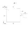
図1に示されるように、半導体モジュールMJの外部には、光通信機器として、レーザ光LZを発光する発光部を有するレーザダイオードチップLDが設けられている。半導体モジュールMJのうち半導体チップCHP1は、直接または光ファイバなどを介して、レーザダイオードチップLDからのレーザ光LZの受光が可能であり、図示はしていないが、半導体モジュールMJ外部に取り付けられる光ファイバなどの光通信機器と光の送受信を行うことができる。すなわち、半導体モジュールMJは、光の送受信が可能な光通信用のインターポーザであるとも言える。 As shown in FIG. 1, a laser diode chip LD having a light emitting unit that emits laser light LZ is provided as an optical communication device outside the semiconductor module MJ. Among the semiconductor modules MJ, the semiconductor chip CHP1 can receive the laser light LZ from the laser diode chip LD directly or via an optical fiber. Although not shown, the light is attached to the outside of the semiconductor module MJ. Light can be transmitted / received to / from an optical communication device such as a fiber. That is, it can be said that the semiconductor module MJ is an optical communication interposer capable of transmitting and receiving light.
また、後で詳細に説明するが、半導体チップCHP1の平面サイズは、半導体チップCHP2の平面サイズとほぼ同じである。図1に示されるように、平面視において、半導体モジュールMJは、X方向に沿った第1辺S1および第2辺S2、並びに、Y方向に沿った第3辺S3および第4辺S4を有し、半導体チップCHP1および半導体チップCHP2も、これらに対応する第1辺S1〜第4辺S4を有する。なお、X方向およびY方向は、互いに交差し、互いに直交している。 As will be described in detail later, the planar size of the semiconductor chip CHP1 is substantially the same as the planar size of the semiconductor chip CHP2. As shown in FIG. 1, in a plan view, the semiconductor module MJ has a first side S1 and a second side S2 along the X direction, and a third side S3 and a fourth side S4 along the Y direction. The semiconductor chip CHP1 and the semiconductor chip CHP2 also have a first side S1 to a fourth side S4 corresponding to these. Note that the X direction and the Y direction intersect each other and are orthogonal to each other.
ここで、第1辺S1を用いて例示すると、平面視において、半導体チップCHP1の第1辺S1の位置は、半導体チップCHP2の第1辺S1の位置と、5μm以内の範囲で一致している。このような関係は、各々の第2辺S2〜第4辺S4についても同様である。 Here, using the first side S1 as an example, the position of the first side S1 of the semiconductor chip CHP1 coincides with the position of the first side S1 of the semiconductor chip CHP2 within a range of 5 μm or less in plan view. . Such a relationship is the same for each of the second side S2 to the fourth side S4.
すなわち、平面視において、半導体チップCHP1の外周は、半導体チップCHP2の外周と所定の範囲内で一致し、具体的には、半導体チップCHP2の外周と5μm以内の範囲で一致している。言い換えれば、半導体チップCHP1の側面と、半導体チップCHP2の側面とは、面一である。更に言い換えれば、半導体チップCHP1の第1辺S1〜第4辺S4の位置と、半導体チップCHP2の第1辺S1〜第4辺S4の位置とのずれが、それぞれ5μm以内である。 That is, in plan view, the outer periphery of the semiconductor chip CHP1 coincides with the outer periphery of the semiconductor chip CHP2 within a predetermined range, and specifically coincides with the outer periphery of the semiconductor chip CHP2 within a range of 5 μm or less. In other words, the side surface of the semiconductor chip CHP1 and the side surface of the semiconductor chip CHP2 are flush with each other. In other words, the deviation between the positions of the first side S1 to the fourth side S4 of the semiconductor chip CHP1 and the positions of the first side S1 to the fourth side S4 of the semiconductor chip CHP2 is within 5 μm, respectively.
以降の本実施の形態において、半導体チップCHP1の平面サイズ、および、半導体チップCHP2の平面サイズが、同じ、または、ほぼ同じと記したときは、上述のように、半導体チップCHP1の外周が、半導体チップCHP2の外周と5μm以内の範囲で一致していることを意味する。 In the following embodiment, when the planar size of the semiconductor chip CHP1 and the planar size of the semiconductor chip CHP2 are the same or substantially the same, as described above, the outer periphery of the semiconductor chip CHP1 is the semiconductor This means that it matches the outer periphery of the chip CHP2 within a range of 5 μm or less.
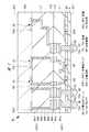
以下に、図2を用いて、本実施の形態の半導体モジュールMJに含まれる半導体チップCHP1および半導体チップCHP2の構造について説明する。図2に示されるように、半導体チップCHP1は、表面TS1および裏面BS1を有し、半導体チップCHP2は、表面TS2および裏面BS2を有している。表面TS1および表面TS2は、向かい合わせになっており、互いに接合している。すなわち、図2では、半導体チップCHP2が逆さになっている状態が示されている。 Hereinafter, the structure of the semiconductor chip CHP1 and the semiconductor chip CHP2 included in the semiconductor module MJ of the present embodiment will be described with reference to FIG. As shown in FIG. 2, the semiconductor chip CHP1 has a front surface TS1 and a back surface BS1, and the semiconductor chip CHP2 has a front surface TS2 and a back surface BS2. The surface TS1 and the surface TS2 face each other and are joined to each other. That is, FIG. 2 shows a state where the semiconductor chip CHP2 is inverted.
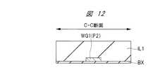
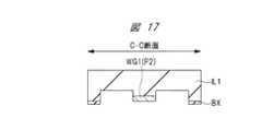
また、図2の断面図において、半導体モジュールMJの側面(半導体チップCHP1の側面)のうち、光導波路WG1に近い側面が、図1に示される辺S4に対応している。 In the cross-sectional view of FIG. 2, the side surface close to the optical waveguide WG1 among the side surfaces of the semiconductor module MJ (side surface of the semiconductor chip CHP1) corresponds to the side S4 shown in FIG.
<半導体チップCHP1の構造>
本実施の形態では、半導体チップCHP1に含まれる主な構成として、光デバイス(光半導体素子)である光導波路WG1、光変調器OMおよび受光器ORが示されている。<Structure of Semiconductor Chip CHP1>
In the present embodiment, an optical waveguide WG1, which is an optical device (optical semiconductor element), an optical modulator OM, and a light receiver OR are shown as main components included in the semiconductor chip CHP1.
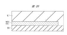
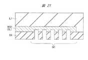
光導波路WG1、光変調器OMおよび受光器ORは、それぞれ絶縁膜BX上に形成されており、同層の半導体層が加工されて形成されている。このような半導体層は、例えばシリコンからなる。また、絶縁層BXは、例えば酸化シリコンからなり、例えば500nm〜3μmの厚さを有する。 The optical waveguide WG1, the optical modulator OM, and the light receiver OR are each formed on the insulating film BX, and are formed by processing the same semiconductor layer. Such a semiconductor layer is made of, for example, silicon. The insulating layer BX is made of, for example, silicon oxide and has a thickness of, for example, 500 nm to 3 μm.
光導波路WG1は、主に、各光デバイスを光学的に接続するための光信号の伝搬路であり、例えば半導体層からなる。本実施の形態の図面では詳細に図示していないが、光導波路WG1は、光変調器OMおよび受光器ORのような他の光デバイスと接続されている。 The optical waveguide WG1 is mainly an optical signal propagation path for optically connecting the optical devices, and is made of, for example, a semiconductor layer. Although not shown in detail in the drawings of the present embodiment, the optical waveguide WG1 is connected to other optical devices such as an optical modulator OM and a light receiver OR.
光変調器OMを構成する半導体層は、例えば、p型、i型(真性半導体)およびn型の領域を含み、これらによってpin構造が構成されている。そして、p型およびn型の領域は、プラグなどを介して、それぞれ上層の配線M1aに電気的に接続されている。この配線M1aから供給される電圧により、半導体層内のキャリア密度を変化させることで、半導体層内の屈折率が変化する。これにより、光変調器OMを伝搬する光に対する実効的な屈折率が変化して、光変調器OMから出力される光の位相を変化させることができる。 The semiconductor layer constituting the optical modulator OM includes, for example, p-type, i-type (intrinsic semiconductor), and n-type regions, and a pin structure is constituted by these. The p-type and n-type regions are electrically connected to the upper wiring M1a through plugs or the like. By changing the carrier density in the semiconductor layer by the voltage supplied from the wiring M1a, the refractive index in the semiconductor layer changes. As a result, the effective refractive index for the light propagating through the optical modulator OM changes, and the phase of the light output from the optical modulator OM can be changed.
受光器ORは、例えばp型の不純物が導入された半導体層と、このp型の半導体層上に形成され、その表面がn型であるi型のゲルマニウム層とを含み、これらによってpin構造が構成されている。n型のゲルマニウム層およびp型の半導体層は、プラグなどを介して、それぞれ上層の配線M1aに電気的に接続されている。これによって、pin構造おいて光起電力効果により流れる直流電流を、受光器ORの外部に取り出すことができる。 The optical receiver OR includes, for example, a semiconductor layer into which a p-type impurity is introduced, and an i-type germanium layer formed on the p-type semiconductor layer and having an n-type surface, thereby forming a pin structure. It is configured. The n-type germanium layer and the p-type semiconductor layer are each electrically connected to the upper wiring M1a via a plug or the like. As a result, a direct current flowing due to the photovoltaic effect in the pin structure can be taken out of the light receiver OR.
また、後で説明するが、半導体チップCHP1では、半導体チップCHP1の裏面BS1において、半導体基板SB1が除去されている。このため、受光器ORは、裏面BS1側において、半導体モジュールMJ外部の光通信機器からの光を受光することができる。 As will be described later, in the semiconductor chip CHP1, the semiconductor substrate SB1 is removed from the back surface BS1 of the semiconductor chip CHP1. For this reason, the light receiver OR can receive light from the optical communication device outside the semiconductor module MJ on the back surface BS1 side.
光導波路WG1、光変調器OMおよび受光器ORの上方には、例えば酸化シリコンからなる層間絶縁膜IL1が形成されている。このように、光導波路WG1、光変調器OMおよび受光器ORの各々の周囲は、互いに同じ材料からなる絶縁膜BXおよび層間絶縁膜IL1に覆われている。そして、絶縁膜BXおよび層間絶縁膜IL1は、光導波路WG1、光変調器OMおよび受光器ORを構成する材料の屈折率よりも、低い屈折率を有する材料からなる。このため、光導波路WG1、光変調器OMおよび受光器ORは、光デバイスのコア層として機能し、絶縁膜BXおよび層間絶縁膜IL1は、光デバイスのクラッド層として機能する。 An interlayer insulating film IL1 made of, for example, silicon oxide is formed above the optical waveguide WG1, the optical modulator OM, and the light receiver OR. In this way, the periphery of each of the optical waveguide WG1, the optical modulator OM, and the light receiver OR is covered with the insulating film BX and the interlayer insulating film IL1 made of the same material. The insulating film BX and the interlayer insulating film IL1 are made of a material having a refractive index lower than that of the material constituting the optical waveguide WG1, the optical modulator OM, and the light receiver OR. For this reason, the optical waveguide WG1, the optical modulator OM, and the light receiver OR function as a core layer of the optical device, and the insulating film BX and the interlayer insulating film IL1 function as a cladding layer of the optical device.
層間絶縁膜IL1中には、1層目の配線M1aと、配線M1aの上方に2層目の配線M2aが形成されている。層間絶縁膜IL1は、実際には多層の絶縁膜の積層膜からなり、配線M1aおよび配線M2aは、各層の絶縁膜中に形成されているが、本実施の形態では、このような多層の絶縁膜を層間絶縁膜IL1として図示している。光デバイスは、配線M1aおよび配線M2aに電気的に接続されている。配線M1aおよび配線M2aは、所謂ダマシン構造またはデュアルダマシン構造の配線であり、銅を主体とした導電性膜からなる。ダマシン構造またはデュアルダマシン構造とは、層間絶縁膜IL1などの絶縁膜に溝を形成し、この溝内に窒化タンタル膜などのバリアメタル膜を介して、銅を主体とした導電性膜を埋め込み、その後、溝外のバリアメタル膜および導電性膜を、CMP(chemical mechanical polishing)法によって除去することで形成される配線構造である。 In the interlayer insulating film IL1, a first layer wiring M1a and a second layer wiring M2a are formed above the wiring M1a. The interlayer insulating film IL1 is actually composed of a multilayer film of multilayer insulating films, and the wiring M1a and the wiring M2a are formed in the insulating films of the respective layers. In this embodiment, such a multilayer insulating film is used. The film is illustrated as an interlayer insulating film IL1. The optical device is electrically connected to the wiring M1a and the wiring M2a. The wiring M1a and the wiring M2a are wiring having a so-called damascene structure or dual damascene structure, and are made of a conductive film mainly composed of copper. In the damascene structure or dual damascene structure, a groove is formed in an insulating film such as an interlayer insulating film IL1, and a conductive film mainly composed of copper is embedded in the groove through a barrier metal film such as a tantalum nitride film. Thereafter, the barrier metal film and the conductive film outside the trench are removed by CMP (chemical mechanical polishing) method.
光デバイスの下方には絶縁膜BXが形成されているが、絶縁膜BXの下面には、更に、例えば酸化シリコンからなる絶縁膜IFが形成されている。 An insulating film BX is formed below the optical device, but an insulating film IF made of, for example, silicon oxide is further formed on the lower surface of the insulating film BX.
絶縁膜BXと、光導波路WG1、光変調器OMおよび受光器ORなどに使用される半導体層とは、元々、SOI(Silicon on Insulator)基板の一部である。本実施の形態では、SOI基板の支持基板である半導体基板SB1を除去している。この時、絶縁膜BXの一部も除去され、絶縁膜BXの厚さが薄くなり、絶縁膜BXがクラッド層として機能できる程度の厚さを保てなくなる恐れがある。このため、絶縁膜IFは、半導体チップCHP1の裏面BS1側において、クラッド層としての役目も果たす。なお、この目的が絶縁膜BXのみで十分に達成できるならば、本実施の形態において、絶縁膜IFは必須ではない。 The insulating film BX and the semiconductor layers used for the optical waveguide WG1, the optical modulator OM, the light receiver OR, and the like are originally part of an SOI (Silicon on Insulator) substrate. In the present embodiment, the semiconductor substrate SB1, which is a support substrate for the SOI substrate, is removed. At this time, part of the insulating film BX is also removed, the thickness of the insulating film BX becomes thin, and there is a possibility that the insulating film BX cannot maintain a thickness that can function as a cladding layer. Therefore, the insulating film IF also serves as a cladding layer on the back surface BS1 side of the semiconductor chip CHP1. Note that the insulating film IF is not essential in the present embodiment if this object can be sufficiently achieved only by the insulating film BX.
絶縁膜IFの下面側(半導体チップCHP1の裏面BS1側)には、例えば銅膜またはアルミニウム膜を有するパッド電極PADが形成されている。また、パッド電極PADは、貫通電極TGVを介して、配線M1aに電気的に接続されている。貫通電極TGVは、裏面BS1側から配線M1aに達するように、絶縁膜BXおよび絶縁膜IFを貫通し、層間絶縁膜IL1の一部が除去されることで形成された孔内に、例えば銅からなる導電性膜を埋め込むことで構成される。 A pad electrode PAD having, for example, a copper film or an aluminum film is formed on the lower surface side of the insulating film IF (the back surface BS1 side of the semiconductor chip CHP1). The pad electrode PAD is electrically connected to the wiring M1a through the through electrode TGV. The through electrode TGV penetrates the insulating film BX and the insulating film IF so as to reach the wiring M1a from the back surface BS1 side, and is formed from, for example, copper in a hole formed by removing a part of the interlayer insulating film IL1. It is configured by embedding a conductive film.
パッド電極PADの下面には、外部接続用端子として、例えば半田からなるバンプ電極BEが形成されている。図示はしていないが、このバンプ電極BEは、他の配線基板または他の半導体チップなどに接続される。従って、半導体チップCHP1は、他の配線基板または他の半導体チップなどのような半導体モジュールMJ外部の電気機器と、電気信号の伝達を行うことができる。 On the lower surface of the pad electrode PAD, a bump electrode BE made of, for example, solder is formed as an external connection terminal. Although not shown, the bump electrode BE is connected to another wiring board or another semiconductor chip. Therefore, the semiconductor chip CHP1 can transmit an electric signal to / from an electric device outside the semiconductor module MJ such as another wiring board or another semiconductor chip.
<半導体チップCHP2の構造>
本実施の形態では、半導体チップCHP2に含まれる主な構成として、半導体素子であるMISFET1Q〜3Qとが示されている。<Structure of semiconductor chip CHP2>
In the present embodiment,
半導体チップCHP2の裏面BS2側には、p型の不純物が導入されたシリコンからなる半導体基板(基板)SB2が設けられている。従って、半導体基板SB2の裏面は、半導体チップCHP2の裏面BS2である。 On the back surface BS2 side of the semiconductor chip CHP2, a semiconductor substrate (substrate) SB2 made of silicon into which p-type impurities are introduced is provided. Therefore, the back surface of the semiconductor substrate SB2 is the back surface BS2 of the semiconductor chip CHP2.
半導体基板SB2の表面には、p型のウェル領域PW1〜PW3、および、n型のウェル領域NWが形成されている。本実施の形態では、ウェル領域PW1にMISFET1Qが形成され、ウェル領域PW2にMISFET2Qが形成され、ウェル領域PW3に容量素子が形成され、ウェル領域NWにMISFET3Qが形成されている例を示している。これらのMISFET1Q〜3Qは、半導体チップCHP2内に形成されている電気回路の一部を構成する半導体素子である。 On the surface of the semiconductor substrate SB2, p-type well regions PW1 to PW3 and an n-type well region NW are formed. In the present embodiment, an example is shown in which the
なお、詳細な説明は省略するが、MISFET1QおよびMISFET2Qは、n型のトランジスタであり、n型のソース領域、n型のドレイン領域、ゲート絶縁膜およびゲート電極を有する。また、MISFET3Qは、p型のトランジスタであり、p型のソース領域、p型のドレイン領域、ゲート絶縁膜およびゲート電極を有する。ウェル領域PW3は、n型の拡散領域およびp型の拡散領域を有する容量素子を構成し、この容量素子は、例えばアナログ回路のACハイパスフィルタの一部として設けられている。 Although detailed description is omitted, the
半導体基板SB2上には、半導体素子(MISFET1Q〜3Q)を覆うように、層間絶縁膜IL2が形成されており、層間絶縁膜IL2中には、半導体素子の上方に多層配線層が形成されている。図2では、このような多層配線層として、配線M1b〜M6bが示されており、半導体素子は配線M1b〜M6bに電気的に接続されている。これらの配線M1b〜M6bの構造は、半導体チップCHP1の配線M1aおよび配線M2aと同様に、例えばダマシン構造またはデュアルダマシン構造である。層間絶縁膜IL2は、実際には多層の絶縁膜の積層膜からなり、配線M1b〜M6bは、各層の絶縁膜中に形成されているが、本実施の形態では、このような多層の絶縁膜を層間絶縁膜IL2として図示している。 An interlayer insulating film IL2 is formed on the semiconductor substrate SB2 so as to cover the semiconductor elements (
<半導体モジュールMJの構成および特徴>
本実施の形態における半導体モジュールMJは、半導体チップCHP1および半導体チップCHP2を有し、半導体チップCHP1の表面TS1および半導体チップCHP2の表面TS2が、互いに接合している。具体的には、半導体チップCHP1の層間絶縁膜IL1の上面が、半導体チップCHP2の層間絶縁膜IL2の上面と接合し、半導体チップCHP1の最上層配線である配線M2aの上面が、半導体チップCHP2の最上層配線である配線M6bの上面と接合している。<Configuration and Features of Semiconductor Module MJ>
The semiconductor module MJ in the present embodiment has a semiconductor chip CHP1 and a semiconductor chip CHP2, and the surface TS1 of the semiconductor chip CHP1 and the surface TS2 of the semiconductor chip CHP2 are joined to each other. Specifically, the upper surface of the interlayer insulating film IL1 of the semiconductor chip CHP1 is joined to the upper surface of the interlayer insulating film IL2 of the semiconductor chip CHP2, and the upper surface of the wiring M2a that is the uppermost layer wiring of the semiconductor chip CHP1 is connected to the upper surface of the semiconductor chip CHP2. It is joined to the upper surface of the wiring M6b which is the uppermost layer wiring.
このように、半導体チップCHP1および半導体チップCHP2は、互いに直接接している配線M2aおよび配線M6bを介して、電気信号の伝達を行うことができる。また、半導体チップCHP1のバンプ電極BEを介して、半導体チップCHP1外部の電気機器(他の配線基板または他の半導体チップなど)から半導体チップCHP2へ、電気信号の伝達を行うことができる。また、半導体チップCHP1は、レーザダイオードチップLDおよび光ファイバなど、半導体モジュールMJ外部の光通信機器と光の送受信を行うことができる。 As described above, the semiconductor chip CHP1 and the semiconductor chip CHP2 can transmit electric signals through the wiring M2a and the wiring M6b that are in direct contact with each other. In addition, an electrical signal can be transmitted from an electrical device (another wiring board or another semiconductor chip) outside the semiconductor chip CHP1 to the semiconductor chip CHP2 via the bump electrode BE of the semiconductor chip CHP1. The semiconductor chip CHP1 can transmit and receive light to and from an optical communication device outside the semiconductor module MJ, such as a laser diode chip LD and an optical fiber.
以下に、半導体モジュールMJと、半導体モジュールMJ外部の光通信機器および電気機器との通信方法について説明する。 Hereinafter, a communication method between the semiconductor module MJ and an optical communication device and an electric device outside the semiconductor module MJ will be described.
電気信号から光信号へ変換する場合は、まず、半導体モジュールMJ外部の電気機器からの第1電気信号を、バンプ電極BE、貫通電極TGVおよび配線M1aを介して、半導体チップCHP1内で受信する。次に、半導体チップCHP1が受信した第1電気信号を、配線M2aおよび配線M6bを介して、半導体チップCHP1から半導体チップCHP2へ送信する。次に、半導体チップCHP2が受信した第1電気信号を、半導体チップCHP2のMISFET1Q〜3Qなどを用いて、第2電気信号などに加工する。次に、第2電気信号を、半導体チップCHP2から半導体チップCHP1へ送信する。次に、半導体チップCHP1が受信した第2電気信号を、半導体チップCHP1の光デバイス(光導波路WG1、光変調器OMおよび受光器OR)を用いて、光信号へ変換する。その後、光信号が、半導体モジュールMJ外部の光通信機器(光ファイバなど)へ送信される。 When converting an electrical signal to an optical signal, first, a first electrical signal from an electrical device outside the semiconductor module MJ is received in the semiconductor chip CHP1 via the bump electrode BE, the through electrode TGV, and the wiring M1a. Next, the first electrical signal received by the semiconductor chip CHP1 is transmitted from the semiconductor chip CHP1 to the semiconductor chip CHP2 via the wiring M2a and the wiring M6b. Next, the first electric signal received by the semiconductor chip CHP2 is processed into a second electric signal or the like using the
光信号から電気信号へ変換する場合は、上記と逆の通信経路を辿ればよい。すなわち、まず、半導体モジュールMJ外部の光通信機器(レーザダイオードチップLDなど)からの光信号を、半導体チップCHP1で受信する。次に、半導体チップCHP1が受信した光信号を、半導体チップCHP1の光デバイスを用いて、第3電気信号へ変換する。次に、第3電気信号を、半導体チップCHP1から半導体チップCHP2へ送信する。次に、半導体チップCHP2が受信した第3電気信号を、半導体チップCHP2のMISFET1Q〜3Qなどを用いて、第4電気信号などに加工する。その後、第4電気信号が、半導体チップCHP1のバンプ電極BE、貫通電極TGV、配線M1aおよび配線M2aを介して、半導体モジュールMJ外部の電気機器へ送信される。 When converting from an optical signal to an electric signal, the reverse communication path may be followed. That is, first, an optical signal from an optical communication device (such as a laser diode chip LD) outside the semiconductor module MJ is received by the semiconductor chip CHP1. Next, the optical signal received by the semiconductor chip CHP1 is converted into a third electrical signal using the optical device of the semiconductor chip CHP1. Next, the third electrical signal is transmitted from the semiconductor chip CHP1 to the semiconductor chip CHP2. Next, the third electrical signal received by the semiconductor chip CHP2 is processed into a fourth electrical signal or the like using the
また、従来技術においては、上述の先行技術文献などに示されるように、フォトニクスチップである半導体チップCHP1の平面サイズが、ドライバチップである半導体チップCHP2の平面サイズよりも大きくなるように形成されていた。 In the prior art, as shown in the above-mentioned prior art documents, the planar size of the semiconductor chip CHP1 that is a photonics chip is formed to be larger than the planar size of the semiconductor chip CHP2 that is a driver chip. It was.
これに対して、本実施の形態では、図1で説明したように、半導体チップCHP1の平面サイズ、および、半導体チップCHP2の平面サイズは同じである。より具体的には、平面視において、半導体チップCHP1の外周は、半導体チップCHP2の外周と5μm以内の範囲で一致している。 In contrast, in the present embodiment, as described in FIG. 1, the planar size of the semiconductor chip CHP1 and the planar size of the semiconductor chip CHP2 are the same. More specifically, in plan view, the outer periphery of the semiconductor chip CHP1 coincides with the outer periphery of the semiconductor chip CHP2 within a range of 5 μm or less.
従って、半導体チップCHP1と半導体チップCHP2との実装密度が最大となっているので、両チップ間において、単位体積当たりのデータ伝送量を最大化し、データ伝送エネルギーの効率を向上させることができる。従って、半導体チップCHP1および半導体チップCHP2を有する半導体モジュールMJの性能を向上させることができる。 Therefore, since the mounting density of the semiconductor chips CHP1 and CHP2 is maximized, the amount of data transmission per unit volume can be maximized between the two chips, and the efficiency of data transmission energy can be improved. Therefore, the performance of the semiconductor module MJ having the semiconductor chip CHP1 and the semiconductor chip CHP2 can be improved.
また、半導体チップCHP1の平面サイズを、半導体チップCHP2の平面サイズと同じにすることができるので、半導体モジュールMJを高集積化することが可能であり、半導体モジュールMJの微細化を図ることができる。 Further, since the planar size of the semiconductor chip CHP1 can be made the same as the planar size of the semiconductor chip CHP2, the semiconductor module MJ can be highly integrated, and the semiconductor module MJ can be miniaturized. .
また、従来技術においては、上述の先行技術文献などに示されるように、フォトニクスチップが、ドライバチップに層間絶縁膜のみを介して接合されているため、フォトニクスチップおよびドライバチップの接合強度が十分でない。 Further, in the prior art, as shown in the above-mentioned prior art documents and the like, since the photonics chip is bonded to the driver chip only through the interlayer insulating film, the bonding strength between the photonics chip and the driver chip is not sufficient. .
これに対して、本実施の形態では、半導体チップCHP1の表面TS1および半導体チップCHP2の表面TS2において、半導体チップCHP1の配線M2aおよび半導体チップCHP2の配線M6bが互いに直接接合している。このため、半導体チップCHP1と半導体チップCHP2との間の抵抗を最小にすることができるとともに、半導体チップCHP1と半導体チップCHP2の接合強度を高めることができる。従って、上記の半導体チップCHP1と半導体チップCHP2との間のデータ伝送エネルギーの効率を最大にすることができる。また、半導体チップCHP1と半導体チップCHP2との接続は、配線M2aおよび配線M6bからなる積層配線を引き回すことで達成できる。すなわち、厚さの厚い積層配線によって、半導体チップCHP1内および半導体チップCHP2内の所望の箇所まで配線を引き回せるため、設計の自由度が増し、配線抵抗を低く抑制することができる。 On the other hand, in the present embodiment, the wiring M2a of the semiconductor chip CHP1 and the wiring M6b of the semiconductor chip CHP2 are directly joined to each other on the surface TS1 of the semiconductor chip CHP1 and the surface TS2 of the semiconductor chip CHP2. For this reason, the resistance between the semiconductor chip CHP1 and the semiconductor chip CHP2 can be minimized, and the bonding strength between the semiconductor chip CHP1 and the semiconductor chip CHP2 can be increased. Therefore, the efficiency of data transmission energy between the semiconductor chip CHP1 and the semiconductor chip CHP2 can be maximized. Further, the connection between the semiconductor chip CHP1 and the semiconductor chip CHP2 can be achieved by drawing a laminated wiring composed of the wiring M2a and the wiring M6b. That is, since the wiring can be routed to a desired location in the semiconductor chip CHP1 and the semiconductor chip CHP2 by the thick laminated wiring, the degree of design freedom is increased, and the wiring resistance can be suppressed low.
<半導体モジュールMJの製造方法>
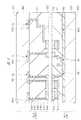
以下に、図3〜図6を用いて、本実施の形態の半導体モジュールMJの製造方法を説明する。なお、図3〜図6では、最終的に図2の半導体モジュールMJが形成される領域に着目して説明するが、図3〜図6は、実際には、半導体モジュールMJが形成される領域を複数備えるウェハ状態における製造工程の断面図となっている。<Method for Manufacturing Semiconductor Module MJ>
Below, the manufacturing method of the semiconductor module MJ of this Embodiment is demonstrated using FIGS. 3 to 6 will be described focusing attention on a region where the semiconductor module MJ of FIG. 2 is finally formed, FIG. 3 to FIG. 6 are actually regions where the semiconductor module MJ is formed. It is sectional drawing of the manufacturing process in the wafer state provided with two or more.
まず、図3に示されるように、半導体チップCHP1となる領域を複数有するウェハWF1と、半導体チップCHP2となる領域を複数有するウェハWF2とを、それぞれ準備する。 First, as shown in FIG. 3, a wafer WF1 having a plurality of regions to be semiconductor chips CHP1 and a wafer WF2 having a plurality of regions to be semiconductor chips CHP2 are prepared.
ウェハWF1では、半導体基板SB1上に絶縁膜BXが形成され、絶縁膜BX上に光デバイス(光導波路WG1、光変調器OMおよび受光器ORなど)、層間絶縁膜IL1、配線M1aおよび配線M2aが形成されている。なお、半導体基板SB1、絶縁膜BX、並びに、光導波路WG1、光変調器OMおよび受光器ORなどに使用される半導体層は、それぞれ、SOI基板の一部である。 In wafer WF1, insulating film BX is formed on semiconductor substrate SB1, and optical devices (such as optical waveguide WG1, optical modulator OM, and light receiver OR), interlayer insulating film IL1, wiring M1a, and wiring M2a are formed on insulating film BX. Is formed. Note that the semiconductor layers used for the semiconductor substrate SB1, the insulating film BX, the optical waveguide WG1, the optical modulator OM, the light receiver OR, and the like are each part of the SOI substrate.
ウェハWF2では、半導体基板SB2上にMISFET1Q〜3Qが形成され、MISFET1Q〜3Q上に、層間絶縁膜IL2および配線M2a〜M6bが形成されている。 In the wafer WF2,
このようなウェハWF1およびウェハWF2を準備した後、ウェハWF1の表面TS1と、ウェハWF2の表面TS2とが向き合うように、ウェハWF1に対してウェハWF2を反転させる、または、ウェハWF2に対してウェハWF1を反転させる。 After preparing the wafer WF1 and the wafer WF2, the wafer WF2 is reversed with respect to the wafer WF1 or the wafer WF2 is reversed so that the surface TS1 of the wafer WF1 and the surface TS2 of the wafer WF2 face each other. Invert WF1.
次に、図4に示されるように、ウェハWF1の表面TS1と、ウェハWF2の表面TS2とを互いに接合させる。この時、半導体チップCHP1となる領域が、半導体チップCHP2となる領域と重なるように、ウェハWF1とウェハWF2との位置合わせが行われる。これにより、ウェハWF1の層間絶縁膜IL1および配線M2aが、それぞれ、ウェハWF2の層間絶縁膜IL2および配線M6bに接合される。 Next, as shown in FIG. 4, the surface TS1 of the wafer WF1 and the surface TS2 of the wafer WF2 are bonded to each other. At this time, the wafer WF1 and the wafer WF2 are aligned so that the region to be the semiconductor chip CHP1 overlaps the region to be the semiconductor chip CHP2. Thereby, interlayer insulating film IL1 and wiring M2a of wafer WF1 are bonded to interlayer insulating film IL2 and wiring M6b of wafer WF2, respectively.
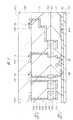
次に、図5に示されるように、ウェハWF1の裏面BS1に対して研磨処理を行い、半導体基板SB1を除去することで、ウェハWF1の裏面BS1側において、絶縁膜BXを露出させる。 Next, as shown in FIG. 5, the back surface BS1 of the wafer WF1 is subjected to a polishing process to remove the semiconductor substrate SB1, thereby exposing the insulating film BX on the back surface BS1 side of the wafer WF1.
次に、絶縁膜BXの下面に、例えばCVD法によって、酸化シリコンからなる絶縁膜IFを形成する。絶縁膜IFの厚さは、例えば1μm〜2μmである。 Next, an insulating film IF made of silicon oxide is formed on the lower surface of the insulating film BX by, for example, a CVD method. The thickness of the insulating film IF is, for example, 1 μm to 2 μm.
なお、必要であれば、これらの工程の前後に、ウェハWF2の裏面BS2を研磨して半導体基板SB2を薄くしてもよい。 If necessary, the semiconductor substrate SB2 may be thinned by polishing the back surface BS2 of the wafer WF2 before and after these steps.
次に、図6に示されるように、まず、ウェハWF1の裏面BS1側から配線M1aに達するように、絶縁膜BXおよび絶縁膜IFを貫通し、層間絶縁膜IL1の一部を除去することで、孔を形成する。次に、この孔内に、例えば銅からなる導電性膜を埋め込む。次に、絶縁膜IFの下面側(ウェハWF1の裏面BS1側)に、例えば銅膜またはアルミニウム膜を含む導電性膜を形成し、この導電性膜をパターニングすることで、パッド電極PADを形成する。次に、パッド電極PADに接するように、例えば半田ボールからなるバンプ電極BEを形成する。 Next, as shown in FIG. 6, first, the insulating film BX and the insulating film IF are penetrated so as to reach the wiring M1a from the back surface BS1 side of the wafer WF1, and a part of the interlayer insulating film IL1 is removed. , Forming holes. Next, a conductive film made of, for example, copper is embedded in the hole. Next, a conductive film including, for example, a copper film or an aluminum film is formed on the lower surface side of the insulating film IF (the back surface BS1 side of the wafer WF1), and the pad electrode PAD is formed by patterning the conductive film. . Next, a bump electrode BE made of, for example, a solder ball is formed so as to be in contact with the pad electrode PAD.
図6の製造工程後、互いに接合しているウェハWF1およびウェハWF2を、ダイシング工程によって個片化することで、図2に示されるような、互いに接合している半導体チップCHP1および半導体チップCHP2が複数個取得される。すなわち、複数の半導体モジュールMJが形成される。 After the manufacturing process of FIG. 6, the wafer WF1 and the wafer WF2 bonded to each other are separated into individual pieces by a dicing process, so that the semiconductor chips CHP1 and CHP2 bonded to each other as shown in FIG. Multiple items are acquired. That is, a plurality of semiconductor modules MJ are formed.
このように、ウェハWF1およびウェハWF2が互いに接合された状態において、ダイシング工程を行っているので、半導体チップCHP1の平面サイズ、および、半導体チップCHP2の平面サイズは同じとなる。 As described above, since the dicing process is performed in the state where the wafer WF1 and the wafer WF2 are bonded to each other, the planar size of the semiconductor chip CHP1 and the planar size of the semiconductor chip CHP2 are the same.
ここで、ダイシング工程には、ブレードまたはレーザによる手法が用いられるが、本願発明者らの検討によれば、これらの手法では、各チップのサイズに多少のばらつきがあることが判った。また、層間絶縁膜IL1および層間絶縁膜IL2のような絶縁膜と、半導体基板SB2のようなシリコンとでは、熱膨張係数が異なるため、ダイシング工程後に、半導体チップCHP1および半導体チップCHP2の各々の平面サイズが変化することもある。 Here, although a technique using a blade or a laser is used for the dicing process, according to the study by the present inventors, it has been found that there is some variation in the size of each chip in these techniques. In addition, since the thermal expansion coefficients are different between the insulating film such as the interlayer insulating film IL1 and the interlayer insulating film IL2 and silicon such as the semiconductor substrate SB2, the respective planes of the semiconductor chip CHP1 and the semiconductor chip CHP2 are obtained after the dicing process. The size may change.
特に、本実施の形態のように、互いに接合されたウェハWF1およびウェハWF2を一括してダイシングする場合、1つの半導体モジュールMJにおける平面サイズのばらつきが大きくなる。このようなばらつきは、5μm以内の範囲である。すなわち、本実施の形態の半導体モジュールMJでは、図1で説明したように、半導体チップCHP1の第1辺S1〜第4辺S4の位置と、半導体チップCHP2の第1辺S1〜第4辺S4の位置とのずれが、それぞれ5μm以内である。 In particular, when the wafers WF1 and WF2 bonded to each other are diced together as in the present embodiment, the variation in the planar size of one semiconductor module MJ increases. Such variation is within a range of 5 μm. That is, in the semiconductor module MJ of the present embodiment, as described in FIG. 1, the positions of the first side S1 to the fourth side S4 of the semiconductor chip CHP1 and the first side S1 to the fourth side S4 of the semiconductor chip CHP2. The deviation from the position of each is within 5 μm.
(実施の形態2)
以下に、実施の形態2の半導体モジュールMJを、図7を用いて説明する。なお、以下の説明では、実施の形態1との相違点を主に説明する。(Embodiment 2)
The semiconductor module MJ according to the second embodiment will be described below with reference to FIG. In the following description, differences from the first embodiment will be mainly described.
図7に示されるように、実施の形態2では、半導体チップCHP1の最上層配線である配線M2aの一部が、ダミー配線DW1として形成され、半導体チップCHP2の最上層配線である配線M6bの一部が、ダミー配線DW2として形成されている。 As shown in FIG. 7, in the second embodiment, a part of the wiring M2a that is the uppermost layer wiring of the semiconductor chip CHP1 is formed as the dummy wiring DW1, and is one of the wirings M6b that is the uppermost layer wiring of the semiconductor chip CHP2. The part is formed as a dummy wiring DW2.
ダミー配線DW1およびダミー配線DW2は、半導体チップCHP1の光デバイス(光導波路WG1、光変調器OMおよび受光器ORなど)、および、半導体チップCHP1のMISFET1Q〜3Qのような半導体素子とは電気的に接続されていない配線であり、フローティング配線である。 The dummy wiring DW1 and the dummy wiring DW2 are electrically different from the optical devices (such as the optical waveguide WG1, the optical modulator OM, and the light receiver OR) of the semiconductor chip CHP1 and the semiconductor elements such as the
このようなダミー配線DW1およびダミー配線DW2を設ける目的は、主に、配線M2aおよび配線M6bを形成する際の研磨処理によるディッシングを防止するためである。すなわち、配線M2aまたは配線M6bと同層の配線層では、互いに隣接する配線の間隔が大きくなると、ディッシングの問題が生じ易い。従って、そのような間隔の広い領域にダミー配線DW1およびダミー配線DW2を設けることで、ディッシングを防止できる。 The purpose of providing the dummy wiring DW1 and the dummy wiring DW2 is mainly to prevent dishing due to the polishing process when forming the wiring M2a and the wiring M6b. That is, in a wiring layer in the same layer as the wiring M2a or the wiring M6b, a problem of dishing is likely to occur when the interval between adjacent wirings is increased. Therefore, dishing can be prevented by providing the dummy wiring DW1 and the dummy wiring DW2 in such a wide-spaced region.
また、実施の形態2では、半導体チップCHP1のダミー配線DW1と、半導体チップCHP2のダミー配線DW2とを、互いに接合するように配置している。ダミー配線DW1を含む配線M2a、および、ダミー配線DW2および配線M6bは、銅を主体とした導電性膜によって構成されている。銅は、層間絶縁膜IL1または層間絶縁膜IL2と直接接していると、層間絶縁膜IL1中または層間絶縁膜IL2中へ拡散し易い傾向がある。ダマシン構造である配線M2aおよび配線M6bは、その側面および底面はバリアメタル膜で囲まれているが、その上面にはバリアメタル膜は形成されていない。そのため、ダミー配線DW1とダミー配線DW2とを、互いに向き合わせることで、ダミー配線DW1とダミー配線DW2に含まれる銅が、層間絶縁膜IL1中または層間絶縁膜IL2中へ拡散されることを、出来るだけ抑制することができる。 In the second embodiment, the dummy wiring DW1 of the semiconductor chip CHP1 and the dummy wiring DW2 of the semiconductor chip CHP2 are arranged so as to be joined to each other. The wiring M2a including the dummy wiring DW1, and the dummy wiring DW2 and the wiring M6b are formed of a conductive film mainly composed of copper. When copper is in direct contact with the interlayer insulating film IL1 or the interlayer insulating film IL2, the copper tends to diffuse into the interlayer insulating film IL1 or the interlayer insulating film IL2. The wiring M2a and the wiring M6b having the damascene structure are surrounded by a barrier metal film on the side surface and the bottom surface, but no barrier metal film is formed on the top surface. Therefore, by making the dummy wiring DW1 and the dummy wiring DW2 face each other, the copper contained in the dummy wiring DW1 and the dummy wiring DW2 can be diffused into the interlayer insulating film IL1 or the interlayer insulating film IL2. Can only be suppressed.
すなわち、ディッシングの抑制だけを目的とするならば、ダミー配線DW1とダミー配線DW2とを互いに接合させる必要はない。しかし、層間絶縁膜IL1中または層間絶縁膜IL2中へ銅の拡散を考慮し、ダミー配線DW1とダミー配線DW2とを互いに接合させることで、半導体モジュールMJ全体の信頼性を向上させることができる。 That is, if the purpose is only to suppress dishing, it is not necessary to join the dummy wiring DW1 and the dummy wiring DW2 to each other. However, the reliability of the entire semiconductor module MJ can be improved by bonding the dummy wiring DW1 and the dummy wiring DW2 to each other in consideration of the diffusion of copper into the interlayer insulating film IL1 or the interlayer insulating film IL2.
更に、金属膜であるダミー配線DW1とダミー配線DW2とを互いに接合させることで、層間絶縁膜IL1と層間絶縁膜IL2とを互いに接合させるよりも、大きな接着力を得ることができる。すなわち、半導体チップCHP1と半導体チップCHP2との接合強度を向上させることができる。 Further, by bonding the dummy wiring DW1 and the dummy wiring DW2 which are metal films to each other, a larger adhesive force can be obtained than when the interlayer insulating film IL1 and the interlayer insulating film IL2 are bonded to each other. That is, the bonding strength between the semiconductor chip CHP1 and the semiconductor chip CHP2 can be improved.
(実施の形態3)
以下に、実施の形態3の半導体モジュールMJおよびその製造方法を、図8〜図13を用いて説明する。なお、以下の説明では、実施の形態1との相違点を主に説明する。(Embodiment 3)
Hereinafter, the semiconductor module MJ of the third embodiment and the manufacturing method thereof will be described with reference to FIGS. In the following description, differences from the first embodiment will be mainly described.
図8に示されるように、実施の形態3では、半導体チップCHP1のうち、レーザダイオードチップLDからのレーザ光LZを受光する側面付近に、スポットサイズコンバータSSCが設けられている。 As shown in FIG. 8, in the third embodiment, a spot size converter SSC is provided in the vicinity of the side surface of the semiconductor chip CHP1 that receives the laser light LZ from the laser diode chip LD.
<スポットサイズコンバータSSCについて>
フォトニクスチップである半導体チップCHP1と、レーザダイオードチップLDとの接続において、光導波路WG1を伝搬する光のスポットサイズと、レーザ光LZのような発光素子のスポットサイズと違いが問題なる場合がある。例えば、互いにスポットサイズの異なる光導波路WG1と発光素子とをそのまま光学的に接続すると、接続部分における光損失が大きくなってしまうという問題が生じる。また、光導波路WG1と光ファイバなどとの接続においても、ほぼ同様の問題が生じる。<About Spot Size Converter SSC>
In the connection between the semiconductor chip CHP1 that is a photonics chip and the laser diode chip LD, there may be a problem between the spot size of light propagating through the optical waveguide WG1 and the spot size of a light emitting element such as the laser beam LZ. For example, if the optical waveguide WG1 having a different spot size and the light emitting element are optically connected as they are, a problem arises that the optical loss at the connection portion increases. In addition, substantially the same problem occurs in the connection between the optical waveguide WG1 and the optical fiber.
例えば、光導波路WG1を伝搬する光のスポットサイズは、サブミクロンのオーダーとなるが、光ファイバや発光素子における光のスポットサイズは、数ミクロンのオーダーとなる。このため、スポットサイズの相対的に小さな光を伝搬する光導波路WG1と、スポットサイズの相対的に大きな光を伝搬する光ファイバまたは発光素子との間に、光のスポットサイズを変換する光デバイスとして、スポットサイズコンバータ(スポットサイズ変換器)SSCを挿入することが有効である。 For example, the spot size of light propagating through the optical waveguide WG1 is on the order of submicrons, but the spot size of light in an optical fiber or a light emitting element is on the order of several microns. Therefore, as an optical device that converts the spot size of light between the optical waveguide WG1 that propagates light having a relatively small spot size and an optical fiber or light emitting element that propagates light having a relatively large spot size. It is effective to insert a spot size converter (spot size converter) SSC.
そこで、図8に示されるように、実施の形態3では、スポットサイズコンバータSSCとして、光導波路WG1の一部に加えて、更に、光導波路WG1の下方に光導波路WG2を設けている。この光導波路WG2は、絶縁膜BXと絶縁膜IF1との間に形成され、例えば窒化シリコンからなる絶縁膜によって形成されている。光導波路WG2の厚さは、例えば1μm〜2μmである。ここで、光導波路WG2は、光が伝搬する経路であり、コア層として機能する。また、絶縁膜BXの下面と、光導波路WG2の下面とは、光導波路WG2を構成する材料の屈折率よりも、低い屈折率を有する材料からなる絶縁膜IFによって覆われている。従って、絶縁膜IFは、クラッド層として機能している。また、光導波路WG2の一方の側面は、絶縁膜IFに覆われておらず、露出している。すなわち、半導体チップCHP2の第4辺S4において、光導波路WG2の一方の側面は、露出しており、レーザダイオードチップLDからレーザ光LZを直接受光できる。 Therefore, as shown in FIG. 8, in the third embodiment, as the spot size converter SSC, in addition to a part of the optical waveguide WG1, an optical waveguide WG2 is further provided below the optical waveguide WG1. The optical waveguide WG2 is formed between the insulating film BX and the insulating film IF1, and is formed of an insulating film made of, for example, silicon nitride. The thickness of the optical waveguide WG2 is, for example, 1 μm to 2 μm. Here, the optical waveguide WG2 is a path through which light propagates, and functions as a core layer. Further, the lower surface of the insulating film BX and the lower surface of the optical waveguide WG2 are covered with an insulating film IF made of a material having a lower refractive index than that of the material constituting the optical waveguide WG2. Therefore, the insulating film IF functions as a cladding layer. Further, one side surface of the optical waveguide WG2 is not covered with the insulating film IF and is exposed. That is, on the fourth side S4 of the semiconductor chip CHP2, one side surface of the optical waveguide WG2 is exposed, and the laser light LZ can be directly received from the laser diode chip LD.
図9は、スポットサイズコンバータSSCの一部を構成する光導波路WG1を拡大した要部平面図を示しており、図10および図11は、それぞれ図9のB−B線およびC−C線に沿った断面を示している。なお、図9のA−A線に沿った断面は、図8に示されるスポットサイズコンバータSSCに対応している。 9 shows an enlarged plan view of a main part of the optical waveguide WG1 constituting a part of the spot size converter SSC. FIGS. 10 and 11 are taken along lines BB and CC in FIG. 9, respectively. A cross section along is shown. The cross section along the line AA in FIG. 9 corresponds to the spot size converter SSC shown in FIG.
図9〜図11に示されるように、光導波路WG1は、光導波路WG1の延在方向(X方向)に沿って、部分P1と部分P2とを有する。平面視において、光導波路WG1の部分P1は、光導波路WG1の延在方向(X方向)と直交する方向(Y方向)の幅がほぼ同じであり、光導波路WG1の部分P2は、Y方向の幅が連続的に狭くなるような、テーパ形状である。 As shown in FIGS. 9 to 11, the optical waveguide WG1 has a portion P1 and a portion P2 along the extending direction (X direction) of the optical waveguide WG1. In plan view, the portion P1 of the optical waveguide WG1 has substantially the same width in the direction (Y direction) orthogonal to the extending direction (X direction) of the optical waveguide WG1, and the portion P2 of the optical waveguide WG1 The taper shape is such that the width is continuously narrowed.
また、実施の形態3では、絶縁膜BXの厚さが、実施の形態1と比較して薄く、例えば30nm〜400nmである。すなわち、光導波路WG1と光導波路WG2との間隔は、例えば30nm〜400nmである。 In the third embodiment, the insulating film BX is thinner than the first embodiment, for example, 30 nm to 400 nm. That is, the distance between the optical waveguide WG1 and the optical waveguide WG2 is, for example, 30 nm to 400 nm.
ここで、光導波路WG1および光導波路WG2は、それぞれ、レーザダイオードチップLDからレーザ光LZを受光する。このとき、光導波路WG1と光導波路WG2との間には、絶縁膜BXが存在しているため、光導波路WG2内を伝搬するレーザ光LZは、光導波路WG1内へは伝搬しないように思われる。例えば、実施の形態1では、光導波路WG1下に形成されている絶縁膜BXは、クラッド層として機能していた。 Here, each of the optical waveguide WG1 and the optical waveguide WG2 receives the laser light LZ from the laser diode chip LD. At this time, since the insulating film BX exists between the optical waveguide WG1 and the optical waveguide WG2, it seems that the laser light LZ propagating in the optical waveguide WG2 does not propagate into the optical waveguide WG1. . For example, in the first embodiment, the insulating film BX formed under the optical waveguide WG1 functions as a cladding layer.
しかしながら、実施の形態3では、エバネッセント光の染み出し距離よりも小さくなるように、絶縁膜BXの厚さを薄くしている。すなわち、光導波路WG1と光導波路WG2との間隔は、例えば30nm〜400nmであり、エバネッセント光の染み出し距離よりも小さい。このため、エバネッセント光によって、光導波路WG2内のレーザ光LZは、光導波路WG2から光導波路WG1へ伝搬することができる。 However, in the third embodiment, the thickness of the insulating film BX is reduced so as to be smaller than the permeation distance of the evanescent light. In other words, the distance between the optical waveguide WG1 and the optical waveguide WG2 is, for example, 30 nm to 400 nm, and is smaller than the evanescent light leakage distance. For this reason, the laser light LZ in the optical waveguide WG2 can be propagated from the optical waveguide WG2 to the optical waveguide WG1 by the evanescent light.
従って、光導波路WG2が受光したレーザ光LZが、光導波路WG2の内部を伝搬するにつれて、光導波路WG2と隣接する光導波路WG1のテーパ部分である部分P2を介して、光導波路WG2から光導波路WG1にレーザ光LZの分布が移動する。このレーザ光LZの分布の移動は、テーパ部分である部分P2の形状に依存する。このように、光導波路WG1を伝搬する光のスポットサイズと、レーザダイオードチップLDなどの光のスポットサイズが異なっていても、スポットサイズコンバータSSCによって、光損失を抑制することができる。 Accordingly, as the laser beam LZ received by the optical waveguide WG2 propagates through the optical waveguide WG2, the optical waveguide WG1 is guided from the optical waveguide WG2 via the portion P2 which is a tapered portion of the optical waveguide WG1 adjacent to the optical waveguide WG2. The distribution of the laser beam LZ moves. The movement of the distribution of the laser beam LZ depends on the shape of the portion P2, which is a tapered portion. Thus, even if the spot size of the light propagating through the optical waveguide WG1 and the spot size of the light such as the laser diode chip LD are different, the light loss can be suppressed by the spot size converter SSC.
<スポットサイズコンバータSSCの製造方法>
以下に、図12および図13を用いて、実施の形態3の半導体モジュールMJの一部であるスポットサイズコンバータSSCの製造工程を説明する。図12および図13は、図9のC−C線に沿った断面であり、実施の形態1の図5で説明した、半導体基板SB1の研磨工程から絶縁膜IFの形成工程までの間の工程に対応している。<Method of manufacturing spot size converter SSC>
The manufacturing process of the spot size converter SSC which is a part of the semiconductor module MJ of the third embodiment will be described below with reference to FIGS. 12 and 13 are cross-sectional views taken along the line C-C in FIG. 9, and the steps from the polishing process of the semiconductor substrate SB1 to the formation process of the insulating film IF described in FIG. 5 of the first embodiment. It corresponds to.
まず、図12に示されるように、実施の形態1の図5で説明した手法と同様に、半導体基板SB1の研磨処理を行い、更にドライエッチング処理を追加することで、絶縁膜BXが露出される。ここで、絶縁膜BXの厚さは、例えば500nm〜3μmとなる。次に、研磨処理を継続し、更にウェットエッチング処理を行うことで、絶縁膜BXの厚さを薄くする。この工程により、絶縁膜BXの厚さは、例えば30nm〜400nm程度となる。 First, as shown in FIG. 12, similarly to the method described with reference to FIG. 5 of the first embodiment, the semiconductor substrate SB1 is subjected to the polishing process, and further the dry etching process is added to expose the insulating film BX. The Here, the thickness of the insulating film BX is, for example, 500 nm to 3 μm. Next, the polishing process is continued, and the wet etching process is further performed to reduce the thickness of the insulating film BX. By this step, the thickness of the insulating film BX becomes, for example, about 30 nm to 400 nm.
次に、図13に示されるように、絶縁膜BXの下面に、例えばCVD法によって、例えば窒化シリコンからなる絶縁膜を形成する。この絶縁膜の厚さは、例えば1μm〜2μmである。次に、フォトリソグラフィ法およびエッチング処理を用いて、この絶縁膜をパターニングすることで、光導波路WG2を形成する。 Next, as shown in FIG. 13, an insulating film made of, for example, silicon nitride is formed on the lower surface of the insulating film BX by, eg, CVD. The thickness of this insulating film is, for example, 1 μm to 2 μm. Next, the optical waveguide WG2 is formed by patterning this insulating film using a photolithography method and an etching process.
その後、実施の形態1の図5で説明した手法と同様に、絶縁膜IFを形成することで、図11の構造が得られる。実施の形態3では、絶縁膜IFは、絶縁膜BXだけでなく、光導波路WG2も覆うように形成される。 Thereafter, similarly to the method described in FIG. 5 of the first embodiment, the structure of FIG. 11 is obtained by forming the insulating film IF. In the third embodiment, the insulating film IF is formed so as to cover not only the insulating film BX but also the optical waveguide WG2.
ここで、光導波路WG1上に光導波路WG2を形成することで、実施の形態3のスポットサイズコンバータSSCと同様なデバイスを形成することも考えられるが、その場合には、光導波路WG1を構成する半導体層上にて、光導波路WG2を形成するために種々のドライエッチング処理などが必要となる。そうすると、光導波路WG1にエッチングダメージが加わる、または、光導波路WG1中にチャージアップが発生するなどの不具合が起こる恐れがある。特に、実施の形態3の光導波路WG2の厚さは、例えば1μm〜2μmであるため、上記ドライエッチング処理を時間の長いオーバーエッチングで行う必要があり、そうすると、上記エッチングダメージおよび上記チャージアップなどの不具合が起こる恐れも大きくなり易い。 Here, it is conceivable to form a device similar to the spot size converter SSC of the third embodiment by forming the optical waveguide WG2 on the optical waveguide WG1, but in this case, the optical waveguide WG1 is configured. Various dry etching processes are required to form the optical waveguide WG2 on the semiconductor layer. In this case, there is a possibility that problems such as etching damage to the optical waveguide WG1 or charge up in the optical waveguide WG1 may occur. In particular, since the thickness of the optical waveguide WG2 of the third embodiment is, for example, 1 μm to 2 μm, it is necessary to perform the dry etching process by long-time over-etching. The risk of failure is likely to increase.
これに対して、実施の形態3では、半導体チップCHP1の裏面BS1側を利用して、光導波路WG1の下に光導波路WG2を形成することができる。そのため、光導波路WG1に対して、上記の不具合を発生させる恐れを抑制することができるので、スポットサイズコンバータSSCの性能を向上させることができる。 On the other hand, in the third embodiment, the optical waveguide WG2 can be formed under the optical waveguide WG1 using the back surface BS1 side of the semiconductor chip CHP1. Therefore, the possibility of causing the above-described problems with respect to the optical waveguide WG1 can be suppressed, so that the performance of the spot size converter SSC can be improved.
また、実施の形態3の技術を、上述の実施の形態2に組み合わせて適用することもできる。 Further, the technique of the third embodiment can be applied in combination with the above-described second embodiment.
(変形例1)
以下に、変形例1の半導体モジュールMJおよびその製造方法を、図14〜図18を用いて説明する。なお、以下の説明では、実施の形態3との相違点を主に説明する。(Modification 1)
Below, the semiconductor module MJ of the
図14に示されるように、変形例1では、実施の形態3と同様の目的で、スポットサイズコンバータSSCが設けられている。しかしながら、変形例1では、実施の形態3と異なり、スポットサイズコンバータSSCを構成する光導波路WG1と光導波路WG2との間において、絶縁膜BXが除去されており、光導波路WG2は光導波路WG1に直接接している。 As shown in FIG. 14, in the first modification, a spot size converter SSC is provided for the same purpose as in the third embodiment. However, in the first modification, unlike the third embodiment, the insulating film BX is removed between the optical waveguide WG1 and the optical waveguide WG2 constituting the spot size converter SSC, and the optical waveguide WG2 becomes the optical waveguide WG1. Direct contact.
なお、スポットサイズコンバータSSCの一部を構成する光導波路WG1の平面図は、実施の形態3で説明した図9と同様であり、図9のA−A線に沿った断面が、図14に示されるスポットサイズコンバータSSCに対応している。また、図15および図16は、それぞれ図9のB−B線およびC−C線に沿った断面を示している。 The plan view of the optical waveguide WG1 constituting a part of the spot size converter SSC is the same as FIG. 9 described in the third embodiment, and the cross section taken along the line AA in FIG. Corresponds to the spot size converter SSC shown. 15 and 16 show cross sections taken along lines BB and CC in FIG. 9, respectively.
図15および図16に示されるように、光導波路WG2である窒化シリコン膜などの絶縁膜は、光導波路WG1の下面だけでなく、光導波路WG1の側面(X方向に沿った側面)も覆っている。そして、光導波路WG2の下面は、絶縁膜IFによって覆われている。 As shown in FIGS. 15 and 16, the insulating film such as a silicon nitride film that is the optical waveguide WG2 covers not only the lower surface of the optical waveguide WG1, but also the side surface (side surface along the X direction) of the optical waveguide WG1. Yes. The lower surface of the optical waveguide WG2 is covered with the insulating film IF.
実施の形態3では、光導波路WG2は光導波路WG1に直接接しているため、光導波路WG2内を伝搬するレーザ光LZは、実施の形態3のようにエバネッセント光を利用することなく、光導波路WG2から光導波路WG1へ容易に伝搬することができる。 In the third embodiment, since the optical waveguide WG2 is in direct contact with the optical waveguide WG1, the laser light LZ propagating in the optical waveguide WG2 does not use the evanescent light as in the third embodiment, and the optical waveguide WG2 Can easily propagate to the optical waveguide WG1.
また、光導波路WG2は、光導波路WG1に直接接しているだけでなく、光導波路WG1の下面および側面も覆っている。従って、仮に、光導波路WG1から漏れる光があったとしても、光導波路WG2によって、その漏れた光を吸収することができる。すなわち、光損失を抑制することができる。 The optical waveguide WG2 not only directly contacts the optical waveguide WG1, but also covers the lower surface and side surfaces of the optical waveguide WG1. Therefore, even if there is light leaking from the optical waveguide WG1, the leaked light can be absorbed by the optical waveguide WG2. That is, light loss can be suppressed.
なお、変形例1では、光導波路WG2の上面の位置が、光導波路WG1の上面の位置よりも高いまで達しているが、光導波路WG2の上面の位置は、光導波路WG1の上面の位置よりも低くてもよい。また、光導波路WG2を光導波路WG1に直接接しさせる目的のみであれば、光導波路WG2の上面の位置は、光導波路WG1の下面の位置と同じであってもよい。すなわち、光導波路WG2の上面の位置は、光導波路WG1の下面の位置と同じか、光導波路WG1の下面の位置より高い。 In
<変形例1のスポットサイズコンバータSSCの製造方法>
以下に、図17および図18を用いて、変形例1の半導体モジュールMJの一部であるスポットサイズコンバータSSCの製造工程を説明する。図17および図18は、図9のC−C線に沿った断面であり、実施の形態3の図12および図13で説明した工程に対応している。<Method for Manufacturing Spot Size Converter SSC of
Hereinafter, a manufacturing process of the spot size converter SSC which is a part of the semiconductor module MJ of the first modification will be described with reference to FIGS. 17 and 18. FIGS. 17 and 18 are cross sections taken along the line CC of FIG. 9 and correspond to the steps described in FIGS. 12 and 13 of the third embodiment.
まず、図17に示されるように、実施の形態1の図5で説明した手法と同様に、半導体基板SB1の研磨処理を行うことで、絶縁膜BXが露出される。次に、フォトリソグラフィ法およびエッチング処理を用いて、スポットサイズコンバータSSCとなる領域の絶縁膜BXを選択的に除去する。そして、更にエッチング処理を継続させることで、層間絶縁膜IL1の一部を除去する。 First, as shown in FIG. 17, the insulating film BX is exposed by performing the polishing process on the semiconductor substrate SB <b> 1 in the same manner as the method described in FIG. 5 of the first embodiment. Next, the insulating film BX in the region to be the spot size converter SSC is selectively removed using a photolithography method and an etching process. Further, by further continuing the etching process, a part of the interlayer insulating film IL1 is removed.
次に、図18に示されるように、絶縁膜BXの下面に、例えばCVD法によって、例えば窒化シリコンからなる絶縁膜を形成する。この絶縁膜の厚さは、例えば1μm〜2μmである。次に、フォトリソグラフィ法およびエッチング処理を用いて、この絶縁膜をパターニングすることで、光導波路WG2を形成する。 Next, as shown in FIG. 18, an insulating film made of, for example, silicon nitride is formed on the lower surface of the insulating film BX by, eg, CVD. The thickness of this insulating film is, for example, 1 μm to 2 μm. Next, the optical waveguide WG2 is formed by patterning this insulating film using a photolithography method and an etching process.
その後、実施の形態1の図5で説明した手法と同様に、絶縁膜IFを形成することで、図16の構造が得られる。変形例1では、絶縁膜IFは、絶縁膜BXだけでなく、光導波路WG2も覆うように形成される。 Thereafter, similarly to the method described in FIG. 5 of the first embodiment, the structure of FIG. 16 is obtained by forming the insulating film IF. In the first modification, the insulating film IF is formed so as to cover not only the insulating film BX but also the optical waveguide WG2.
(実施の形態4)
以下に、実施の形態4の半導体モジュールMJおよびその製造方法を、図19〜図21を用いて説明する。なお、以下の説明では、実施の形態1との相違点を主に説明する。(Embodiment 4)
Hereinafter, the semiconductor module MJ and the manufacturing method thereof according to the fourth embodiment will be described with reference to FIGS. In the following description, differences from the first embodiment will be mainly described.
図19に示されるように、実施の形態4では、半導体チップCHP1内に、光導波路WG1と接続されるグレーティングカプラ(Grating Coupler)GCを設けている。なお、グレーティングカプラGCは、光導波路WG1、光変調器OMおよび受光器ORなどと同層の半導体層を加工することで形成されている。実施の形態4では、便宜上、上記半導体層を半導体層SLとして説明している。 As shown in FIG. 19, in the fourth embodiment, a grating coupler GC connected to the optical waveguide WG1 is provided in the semiconductor chip CHP1. The grating coupler GC is formed by processing the same semiconductor layer as the optical waveguide WG1, the optical modulator OM, the light receiver OR, and the like. In the fourth embodiment, the semiconductor layer is described as the semiconductor layer SL for convenience.
<グレーティングカプラGCについて>
グレーティングカプラGCは、光導波路WG1の1種であり、光導波路WG1を伝搬する光に半導体モジュールMJ外部の光通信機器から入射するレーザ光を結合する、または、光導波路WG1を伝搬する光を半導体モジュールMJ外部の光通信機器へ出射する光デバイスである。<About Grating Coupler GC>
The grating coupler GC is a kind of the optical waveguide WG1, and couples the light propagating from the optical communication device outside the semiconductor module MJ to the light propagating through the optical waveguide WG1, or the light propagating through the optical waveguide WG1 as a semiconductor. This is an optical device that emits light to an optical communication device outside the module MJ.
図19では、グレーティングカプラGCを介して、光導波路WG1から半導体モジュールMJ外部の光通信機器へ光を出射する場合について、光の伝搬経路を模式的に矢印で示している。また、グレーティングカプラGCを介して、半導体モジュールMJ外部の光通信機器から光導波路WG1へ光を入射する場合は、この矢印の向きが逆となる。なお、図19では、光の伝搬経路を判り易くするため、グレーティングカプラGCおよび光導波路WG1の周辺のハッチングを省略している。 In FIG. 19, when light is emitted from the optical waveguide WG1 to the optical communication device outside the semiconductor module MJ via the grating coupler GC, the light propagation path is schematically indicated by arrows. Further, when light is incident on the optical waveguide WG1 from the optical communication device outside the semiconductor module MJ via the grating coupler GC, the direction of this arrow is reversed. In FIG. 19, hatching around the grating coupler GC and the optical waveguide WG1 is omitted in order to make the light propagation path easy to understand.
グレーティングカプラGCを伝搬する光は、光導波路面に、伝搬方向に沿って設けられた凹部(溝部)および凸部(突起部)により、周期的屈折率変調(導波路グレーティング)が行われ、ある特定の方向に回析放射される。実施の形態4では、図19に示されるように、グレーティングカプラGCの凹部および凸部は、半導体チップCHP1の裏面BS1側に向けて設けられている。そのため、光の回折方向は、裏面BS1側に向かう方向が支配的となる。 The light propagating through the grating coupler GC is subjected to periodic refractive index modulation (waveguide grating) by a concave portion (groove portion) and a convex portion (projection portion) provided along the propagation direction on the optical waveguide surface. Diffracted radiation in a specific direction. In the fourth embodiment, as shown in FIG. 19, the concave and convex portions of the grating coupler GC are provided toward the back surface BS1 side of the semiconductor chip CHP1. Therefore, the direction of light diffraction is dominant in the direction toward the back surface BS1.
実施の形態4では、半導体チップCHP1の表面TS1側には、半導体チップCHP2が設けられている。このため、グレーティングカプラGCと、半導体モジュールMJ外部の光通信機器との光通信は、表面TS1側で行うことが困難であり、裏面BS1側で行うことが有効である。ここで、グレーティングカプラGCの下方において、半導体チップCHP1の裏面BS1では、半導体基板SB1が除去され、絶縁膜IFが露出している。このため、グレーティングカプラGCは、裏面BS1側において、半導体モジュールMJ外部の光通信機器と、光通信を行うことができる。そして、上述のように、グレーティングカプラGCの凹部および凸部は、裏面BS1側に向けて設けられているので、上記光の伝搬を効率的に行うことができる。 In the fourth embodiment, the semiconductor chip CHP2 is provided on the surface TS1 side of the semiconductor chip CHP1. For this reason, it is difficult to perform optical communication between the grating coupler GC and the optical communication device outside the semiconductor module MJ on the front surface TS1 side, and it is effective to perform on the back surface BS1 side. Here, below the grating coupler GC, the semiconductor substrate SB1 is removed and the insulating film IF is exposed on the back surface BS1 of the semiconductor chip CHP1. Therefore, the grating coupler GC can perform optical communication with the optical communication device outside the semiconductor module MJ on the back surface BS1 side. As described above, since the concave portion and the convex portion of the grating coupler GC are provided toward the back surface BS1, the light can be efficiently propagated.
<グレーティングカプラGCの製造方法>
以下に、図20および図21を用いて、変形例1の半導体モジュールMJの一部であるグレーティングカプラGCの製造工程を説明する。図20および図21は、グレーティングカプラGCの形成領域を拡大した要部断面図を示しており、実施の形態1の図5で説明した、半導体基板SB1の研磨工程から絶縁膜IFの形成工程までの間の工程に対応している。<Manufacturing method of grating coupler GC>
Hereinafter, a manufacturing process of the grating coupler GC which is a part of the semiconductor module MJ of the first modification will be described with reference to FIGS. FIGS. 20 and 21 are enlarged cross-sectional views showing the principal region where the grating coupler GC is formed. From the polishing step of the semiconductor substrate SB1 to the formation step of the insulating film IF described in FIG. 5 of the first embodiment. It corresponds to the process between.
まず、図20に示されるように、実施の形態1の図5で説明した手法と同様に、半導体基板SB1の研磨処理を行うことで、絶縁膜BXが露出される。 First, as shown in FIG. 20, the insulating film BX is exposed by performing the polishing process on the semiconductor substrate SB <b> 1 in the same manner as the method described in FIG. 5 of the first embodiment.
次に、図21に示されるように、フォトリソグラフィ法およびエッチング処理を用いて、絶縁膜BXの一部を選択的にパターニングする。その後、エッチングガスを変更し、エッチング処理を継続することで、半導体層SLを貫通しないように、半導体層SLに凹部(溝部)を形成する。この時、エッチングされなかった領域が、凸部となる。このように、半導体層SLが加工されて、半導体チップCHP1の裏面BS1側に向けて設けられた凹部および凸部を有するグレーティングカプラGCが形成される。 Next, as shown in FIG. 21, a part of the insulating film BX is selectively patterned by using a photolithography method and an etching process. Thereafter, by changing the etching gas and continuing the etching process, a recess (groove) is formed in the semiconductor layer SL so as not to penetrate the semiconductor layer SL. At this time, a region that has not been etched becomes a convex portion. In this manner, the semiconductor layer SL is processed to form a grating coupler GC having a concave portion and a convex portion provided toward the back surface BS1 side of the semiconductor chip CHP1.
その後、実施の形態1の図5で説明した手法と同様に、絶縁膜IFを形成することで、図16の構造が得られる。絶縁膜IFは、グレーティングカプラGCの凹部および凸部を覆うように形成される。 Thereafter, similarly to the method described in FIG. 5 of the first embodiment, the structure of FIG. 16 is obtained by forming the insulating film IF. The insulating film IF is formed so as to cover the concave and convex portions of the grating coupler GC.
また、実施の形態4の技術を、上述の実施の形態2および実施の形態3に組み合わせて適用することもできる。 Further, the technique of the fourth embodiment can be applied in combination with the above-described second and third embodiments.
(変形例2)
以下に、変形例2の半導体モジュールMJを、図22を用いて説明する。なお、以下の説明では、実施の形態4との相違点を主に説明する。(Modification 2)
Hereinafter, a semiconductor module MJ of
図22に示されるように、変形例2では、実施の形態4と同様の目的で、グレーティングカプラGCが設けられている。そして、変形例2では、グレーティングカプラGCの上方に、反射膜RFが設けられている。言い換えれば、平面視において、グレーティングカプラGCと重なる位置に、反射膜RFが設けられている。 As shown in FIG. 22, in the second modification, a grating coupler GC is provided for the same purpose as in the fourth embodiment. In the second modification, the reflective film RF is provided above the grating coupler GC. In other words, the reflective film RF is provided at a position overlapping the grating coupler GC in plan view.
実施の形態4で説明したように、グレーティングカプラGCの凹部および凸部は、半導体チップCHP1の裏面BS1側に向けて設けられているため、光の回折方向は、裏面BS1側へ向かう方向が支配的である。しかしながら、半導体チップCHP1の裏面BS1側に回析せず、半導体チップCHP1の表面TS1側に回析する光も存在している。具体的には、70%程度の光が裏面BS1側に回析し、30%程度の光が表面TS1側に回析している。この表面TS1側に回析した光は、光損失に直結する。 As described in the fourth embodiment, since the concave and convex portions of the grating coupler GC are provided toward the back surface BS1 side of the semiconductor chip CHP1, the direction of light diffraction is dominated by the direction toward the back surface BS1 side. Is. However, there is also light that does not diffract on the back surface BS1 side of the semiconductor chip CHP1 but diffracts on the front surface TS1 side of the semiconductor chip CHP1. Specifically, about 70% of light is diffracted on the back surface BS1 side, and about 30% of light is diffracted on the front surface TS1 side. The light diffracted on the surface TS1 side is directly connected to optical loss.
反射膜RFは、このような表面TS1側に回析した光を裏面BS1側に反射させ、光損失を抑制するために設けられている。従って、反射膜RFは、グレーティングカプラGCの上面全体を覆っていることが好ましい。 The reflection film RF is provided in order to reflect the light diffracted on the surface TS1 side to the back surface BS1 side and suppress light loss. Therefore, it is preferable that the reflective film RF covers the entire upper surface of the grating coupler GC.
また、このような反射膜RFは、導電性膜によって構成されるが、光の反射率を高めるために、反射膜RFは、金属膜によって構成されていることが好ましい。図22では、反射膜RFが、配線M1aと同じ材料で形成され、配線M1aと同層に形成され、且つ、配線M1aと同じ工程で形成された場合を例示している。この場合、製造工程を簡略化することができる。 In addition, such a reflective film RF is composed of a conductive film, but in order to increase the reflectance of light, the reflective film RF is preferably composed of a metal film. FIG. 22 illustrates a case where the reflective film RF is formed of the same material as the wiring M1a, is formed in the same layer as the wiring M1a, and is formed in the same process as the wiring M1a. In this case, the manufacturing process can be simplified.
また、反射膜RFは、配線M2aと同じ材料で形成され、配線M2aと同層に形成され、且つ、配線M2aと同じ工程で形成されていてもよい。配線M1aまたは配線M2aの選択については、グレーティングカプラGC内を伝搬する光の波長によって、より適切な方を選択することができる。 The reflective film RF may be formed of the same material as the wiring M2a, formed in the same layer as the wiring M2a, and may be formed in the same process as the wiring M2a. As for the selection of the wiring M1a or the wiring M2a, a more appropriate one can be selected depending on the wavelength of light propagating in the grating coupler GC.
また、反射膜RFは、配線M1aまたは配線M2aとは別の導電性膜によって形成されてもよい。このような導電性膜は、配線M1aまたは配線M2aとは別工程によって形成される。この場合、反射膜RFを別途形成するための製造コストが増加するが、反射膜RFの材料は、配線M1aまたは配線M2aに使用される材料に限られず、所望の反射率が得られるように、自由に選択できる。このような導電性膜としては、例えば窒化チタン膜、窒化タンタル膜またはタングステン膜のような金属膜が挙げられる。 The reflective film RF may be formed of a conductive film different from the wiring M1a or the wiring M2a. Such a conductive film is formed in a separate process from the wiring M1a or the wiring M2a. In this case, the manufacturing cost for separately forming the reflective film RF increases, but the material of the reflective film RF is not limited to the material used for the wiring M1a or the wiring M2a, and a desired reflectance can be obtained. You can choose freely. Examples of such a conductive film include a metal film such as a titanium nitride film, a tantalum nitride film, or a tungsten film.
また、変形例2では、図22に示されるように、受光器ORの上方にも反射膜RFを設けている。言い換えれば、平面視において、受光器ORと重なる位置に、反射膜RFが設けられている。実施の形態1で説明したように、半導体チップCHP1の裏面BS1では、半導体基板SB1が除去されているので、受光器ORは、裏面BS1側において、半導体モジュールMJ外部の光通信機器からの光を受光することができる。このとき、受光器ORの上方に反射膜RFが設けられていることで、受光器ORを透過した光を反射させ、反射した光を受光器ORで受光することができる。なお、図22では、光の伝搬経路を判り易くするため、グレーティングカプラGCの周辺と同様に、受光器ORの周辺のハッチングも省略している。 In
また、裏面BS1側において、半導体モジュールMJ外部の光通信機器から半導体チップCHP1(受光器ORおよびグレーティングカプラGC)へ入射させる光の角度は、反射膜RFに対して垂直ではなく、反射膜RFに対する垂線から斜めに傾けた角度とすることが好ましい。この理由は、入射角度が垂直であった場合、入射した光と、反射膜RFから反射した光とが重なり、互いの波長を打ち消しあう恐れがあるからである。 Further, on the back surface BS1 side, the angle of light incident on the semiconductor chip CHP1 (the light receiver OR and the grating coupler GC) from the optical communication device outside the semiconductor module MJ is not perpendicular to the reflective film RF, but relative to the reflective film RF. It is preferable that the angle be inclined obliquely from the normal. This is because when the incident angle is vertical, the incident light and the light reflected from the reflective film RF may overlap and cancel each other's wavelengths.
以上、本願発明者らによってなされた発明をその実施の形態に基づき具体的に説明したが、本発明は上記実施の形態に限定されるものではなく、その要旨を逸脱しない範囲で種々変更可能である。 As mentioned above, the invention made by the inventors of the present application has been specifically described based on the embodiment. However, the present invention is not limited to the embodiment described above, and various modifications can be made without departing from the scope of the invention. is there.
例えば、半導体チップCHP1において、配線M1aのような最上層配線より下層の配線は、ダマシン構造の配線ではなく、窒化チタン膜、アルミニウム膜および窒化チタン膜を積層させ、この積層膜をパターニングすることによって形成された配線であってもよい。この場合、配線の形成し、配線を覆うように層間絶縁膜を形成した後、層間絶縁膜の上面に対してCMP法による研磨処理を行うことによって、層間絶縁膜が平坦化される。 For example, in the semiconductor chip CHP1, the lower layer wiring such as the wiring M1a is not a damascene structure wiring, but a titanium nitride film, an aluminum film, and a titanium nitride film are stacked and this stacked film is patterned. It may be a formed wiring. In this case, after the wiring is formed and the interlayer insulating film is formed so as to cover the wiring, the upper surface of the interlayer insulating film is subjected to a polishing process by a CMP method, thereby planarizing the interlayer insulating film.
また、半導体チップCHP1では、多層配線として、配線M1aおよび配線M2aの2層配線を例示したが、半導体チップCHP1の多層配線は、3層以上であってもよい。また、半導体チップCHP2では、多層配線として、配線M1b〜配線M6bの6層配線を例示したが、半導体チップCHP2の多層配線は、6層より少なくてもよいし、6層より多くてもよい。 Further, in the semiconductor chip CHP1, the two-layer wiring of the wiring M1a and the wiring M2a is illustrated as the multilayer wiring, but the multilayer wiring of the semiconductor chip CHP1 may be three or more layers. In the semiconductor chip CHP2, the six-layer wiring of the wiring M1b to the wiring M6b is illustrated as the multilayer wiring. However, the multilayer wiring of the semiconductor chip CHP2 may be less than six layers or more than six layers.
その他、上記実施の形態に記載された内容の一部を以下に記載する。 In addition, a part of the contents described in the above embodiment will be described below.
[付記1]
光デバイス、前記光デバイスの上方に形成され、且つ、前記光デバイスに電気的に接続された第1配線、および、前記第1配線と同層に形成され、且つ、前記光デバイスに電気的に接続されていない第1ダミー配線を備える第1半導体チップと、
電気回路の一部を構成する半導体素子、前記半導体素子の上方に形成され、且つ、前記半導体素子に電気的に接続された第2配線、および、前記第2配線と同層に形成され、且つ、前記半導体素子に電気的に接続されていない第2ダミー配線を備える第2半導体チップと、
を有し、
前記第2半導体チップは、前記第1半導体チップ上に搭載され、
前記第1配線と前記第2配線とが直接接し、且つ、前記第1ダミー配線と前記第2ダミー配線とが直接接するように、前記第1半導体チップの表面は、前記第2半導体チップの表面と接合している、半導体モジュール。[Appendix 1]
An optical device, a first wiring formed above the optical device and electrically connected to the optical device, and formed in the same layer as the first wiring, and electrically connected to the optical device A first semiconductor chip comprising a first dummy wiring that is not connected;
A semiconductor element constituting a part of an electric circuit, a second wiring formed above the semiconductor element and electrically connected to the semiconductor element, and formed in the same layer as the second wiring; and A second semiconductor chip comprising a second dummy wiring not electrically connected to the semiconductor element;
Have
The second semiconductor chip is mounted on the first semiconductor chip;
The surface of the first semiconductor chip is the surface of the second semiconductor chip so that the first wiring and the second wiring are in direct contact with each other, and the first dummy wiring and the second dummy wiring are in direct contact with each other. A semiconductor module joined with
[付記2]
光デバイス、および、前記光デバイスの上方に形成され、且つ、前記光デバイスに電気的に接続された第1配線を備える第1半導体チップと、
電気回路の一部を構成する半導体素子、および、前記半導体素子の上方に形成され、且つ、前記半導体素子に電気的に接続された第2配線を備える第2半導体チップと、
を有し、
前記第2半導体チップは、前記第1半導体チップ上に搭載され、
前記第1配線と前記第2配線とが直接接するように、前記第1半導体チップの表面は、前記第2半導体チップの表面と接合し、
前記光デバイスは、半導体層からなる第1光導波路と、少なくとも前記第1光導波路の下方に形成され、且つ、絶縁膜からなる第2光導波路とを有する、半導体モジュール。[Appendix 2]
A first semiconductor chip comprising an optical device and a first wiring formed above the optical device and electrically connected to the optical device;
A semiconductor element constituting a part of an electric circuit, and a second semiconductor chip including a second wiring formed above the semiconductor element and electrically connected to the semiconductor element;
Have
The second semiconductor chip is mounted on the first semiconductor chip;
The surface of the first semiconductor chip is bonded to the surface of the second semiconductor chip so that the first wiring and the second wiring are in direct contact with each other.
The optical device includes a first optical waveguide made of a semiconductor layer, and a second optical waveguide formed at least below the first optical waveguide and made of an insulating film.
[付記3]
光デバイス、および、前記光デバイスの上方に形成され、且つ、前記光デバイスに電気的に接続された第1配線を備える第1半導体チップと、
電気回路の一部を構成する半導体素子、および、前記半導体素子の上方に形成され、且つ、前記半導体素子に電気的に接続された第2配線を備える第2半導体チップと、
を有し、
前記第2半導体チップは、前記第1半導体チップ上に搭載され、
前記第1配線と前記第2配線とが直接接するように、前記第1半導体チップの表面は、前記第2半導体チップの表面と接合し、
前記光デバイスは、凹部および凸部を有するグレーティングカプラを含み、
前記グレーティングカプラの前記凹部および前記凸部は、前記第1半導体チップの裏面側に向けて設けられている、半導体モジュール。[Appendix 3]
A first semiconductor chip comprising an optical device and a first wiring formed above the optical device and electrically connected to the optical device;
A semiconductor element constituting a part of an electric circuit, and a second semiconductor chip including a second wiring formed above the semiconductor element and electrically connected to the semiconductor element;
Have
The second semiconductor chip is mounted on the first semiconductor chip;
The surface of the first semiconductor chip is bonded to the surface of the second semiconductor chip so that the first wiring and the second wiring are in direct contact with each other.
The optical device includes a grating coupler having a concave portion and a convex portion,
The semiconductor module, wherein the concave portion and the convex portion of the grating coupler are provided toward a back surface side of the first semiconductor chip.
[付記4]
光デバイス、および、前記光デバイスの上方に形成され、且つ、前記光デバイスに電気的に接続された第1配線を備える第1半導体チップと、
電気回路の一部を構成する半導体素子、および、前記半導体素子の上方に形成され、且つ、前記半導体素子に電気的に接続された第2配線を備える第2半導体チップと、
を有し、
前記第2半導体チップは、前記第1半導体チップ上に搭載され、
前記第1配線と前記第2配線とが直接接するように、前記第1半導体チップの表面が、前記第2半導体チップの表面と接合している、半導体モジュールを用いた通信方法において、
前記半導体モジュール外部の電気機器からの第1電気信号を、前記第1半導体チップで受信する工程、
前記第1半導体チップが受信した前記第1電気信号を、前記第1半導体チップから前記第2半導体チップへ送信する工程、
前記第2半導体チップが受信した前記第1電気信号を、前記半導体素子を用いて、第2電気信号に加工する工程、
前記第2電気信号を、第2半導体チップから前記第1半導体チップへ送信する工程、
前記第1半導体チップが受信した前記第2電気信号を、前記光デバイスを用いて、光信号へ変換する工程、
前記光信号を、前記第1半導体チップから前記半導体モジュール外部の光通信機器へ送信する工程、を有する、通信方法。[Appendix 4]
A first semiconductor chip comprising an optical device and a first wiring formed above the optical device and electrically connected to the optical device;
A semiconductor element constituting a part of an electric circuit, and a second semiconductor chip including a second wiring formed above the semiconductor element and electrically connected to the semiconductor element;
Have
The second semiconductor chip is mounted on the first semiconductor chip;
In the communication method using a semiconductor module, the surface of the first semiconductor chip is bonded to the surface of the second semiconductor chip so that the first wiring and the second wiring are in direct contact with each other.
Receiving a first electric signal from an electric device outside the semiconductor module by the first semiconductor chip;
Transmitting the first electrical signal received by the first semiconductor chip from the first semiconductor chip to the second semiconductor chip;
Processing the first electrical signal received by the second semiconductor chip into a second electrical signal using the semiconductor element;
Transmitting the second electrical signal from a second semiconductor chip to the first semiconductor chip;
Converting the second electrical signal received by the first semiconductor chip into an optical signal using the optical device;
Transmitting the optical signal from the first semiconductor chip to an optical communication device outside the semiconductor module.
[付記5]
光デバイス、および、前記光デバイスの上方に形成され、且つ、前記光デバイスに電気的に接続された第1配線を備える第1半導体チップと、
電気回路の一部を構成する半導体素子、および、前記半導体素子の上方に形成され、且つ、前記半導体素子に電気的に接続された第2配線を備える第2半導体チップと、
を有し、
前記第2半導体チップは、前記第1半導体チップ上に搭載され、
前記第1配線と前記第2配線とが直接接するように、前記第1半導体チップの表面が、前記第2半導体チップの表面と接合している、半導体モジュールを用いた通信方法において、
前記半導体モジュール外部の光通信機器からの光信号を、前記第1半導体チップで受信する工程、
前記第1半導体チップが受信した前記光信号を、前記光デバイスを用いて、第3電気信号へ変換する工程、
前記第3電気信号を、前記第1半導体チップから前記第2半導体チップへ送信する工程、
前記第2半導体チップが受信した前記第3電気信号を、前記半導体素子を用いて、第4電気信号に加工する工程、
第4電気信号を、前記外部接続用端子および前記貫通電極を介して、前記半導体モジュール外部の電気機器へ送信する工程、を有する、通信方法。[Appendix 5]
A first semiconductor chip comprising an optical device and a first wiring formed above the optical device and electrically connected to the optical device;
A semiconductor element constituting a part of an electric circuit, and a second semiconductor chip including a second wiring formed above the semiconductor element and electrically connected to the semiconductor element;
Have
The second semiconductor chip is mounted on the first semiconductor chip;
In the communication method using a semiconductor module, the surface of the first semiconductor chip is bonded to the surface of the second semiconductor chip so that the first wiring and the second wiring are in direct contact with each other.
Receiving an optical signal from an optical communication device outside the semiconductor module by the first semiconductor chip;
Converting the optical signal received by the first semiconductor chip into a third electrical signal using the optical device;
Transmitting the third electrical signal from the first semiconductor chip to the second semiconductor chip;
Processing the third electrical signal received by the second semiconductor chip into a fourth electrical signal using the semiconductor element;
Transmitting a fourth electrical signal to an electrical device outside the semiconductor module via the external connection terminal and the through electrode.
[付記6]
光デバイス、および、前記光デバイスの上方に形成され、且つ、前記光デバイスに電気的に接続された第1配線を備える第1半導体チップと、
電気回路の一部を構成する半導体素子、および、前記半導体素子の上方に形成され、且つ、前記半導体素子に電気的に接続された第2配線を備える第2半導体チップと、
を有する半導体モジュールにおいて、
前記第2半導体チップは、前記第1半導体チップ上に搭載され、
前記第1配線と前記第2配線とが直接接するように、前記第1半導体チップの表面が、前記第2半導体チップの表面と接合し、
前記第1半導体チップCHP1の裏面側において、前記半導体モジュール外部の電気機器および光通信機器と、それぞれ電気信号および光信号の伝達が可能である、半導体モジュール。[Appendix 6]
A first semiconductor chip comprising an optical device and a first wiring formed above the optical device and electrically connected to the optical device;
A semiconductor element constituting a part of an electric circuit, and a second semiconductor chip including a second wiring formed above the semiconductor element and electrically connected to the semiconductor element;
In a semiconductor module having
The second semiconductor chip is mounted on the first semiconductor chip;
The surface of the first semiconductor chip is joined to the surface of the second semiconductor chip so that the first wiring and the second wiring are in direct contact with each other,
A semiconductor module capable of transmitting an electric signal and an optical signal to an electric device and an optical communication device outside the semiconductor module on the back surface side of the first semiconductor chip CHP1.
1Q〜3Q MISFET
BE バンプ電極
BS1、BS2 裏面
BX 絶縁膜
CHP1、CHP2 半導体チップ
DW1、DW2 ダミー配線
GC グレーティングカプラ
IF 絶縁膜
IL1、IL2 層間絶縁膜
LD レーザダイオードチップ
LZ レーザ光
M1a、M2a 配線
M1b〜M6b 配線
MJ 半導体モジュール
NW ウェル領域
OM 光変調器
OR 受光器
P1、P2 部分
PAD パッド電極
PW1〜PW3 ウェル領域
RF 反射膜
S1〜S4 辺
SB1、SB2 半導体基板
SL 半導体層
SSC スポットサイズコンバータ
TGV 貫通電極
TS1、TS2 表面
WF1、WF2 ウェハ
WG1、WG2 光導波路1Q-3Q MISFET
BE Bump electrodes BS1, BS2 Back surface BX Insulating film CHP1, CHP2 Semiconductor chip DW1, DW2 Dummy wiring GC Grating coupler IF Insulating film IL1, IL2 Interlayer insulating film LD Laser diode chip LZ Laser light M1a, M2a wiring M1b-M6b wiring MJ Semiconductor module NW Well region OM Optical modulator OR Receiver P1, P2 Partial PAD Pad electrode PW1-PW3 Well region RF Reflective film S1-S4 Side SB1, SB2 Semiconductor substrate SL Semiconductor layer SSC Spot size converter TGV Through electrode TS1, TS2 Surface WF1, WF2 Wafer WG1, WG2 Optical waveguide
Claims (20)
Translated fromJapanese電気回路の一部を構成する半導体素子、および、前記半導体素子の上方に形成され、且つ、前記半導体素子に電気的に接続された第2配線を備える第2半導体チップと、
を有し、
前記第2半導体チップは、前記第1半導体チップ上に搭載され、
前記第1配線と前記第2配線とが直接接するように、前記第1半導体チップの表面は、前記第2半導体チップの表面と接合している、半導体モジュール。A first semiconductor chip comprising an optical device and a first wiring formed above the optical device and electrically connected to the optical device;
A semiconductor element constituting a part of an electric circuit, and a second semiconductor chip including a second wiring formed above the semiconductor element and electrically connected to the semiconductor element;
Have
The second semiconductor chip is mounted on the first semiconductor chip;
A semiconductor module, wherein a surface of the first semiconductor chip is bonded to a surface of the second semiconductor chip so that the first wiring and the second wiring are in direct contact with each other.
平面視において、前記第1半導体チップの外周は、前記第2半導体チップの外周と5μm以内の範囲で一致している、半導体モジュール。The semiconductor module according to claim 1,
In a plan view, the outer periphery of the first semiconductor chip is coincident with the outer periphery of the second semiconductor chip within a range of 5 μm or less.
平面視において、前記第1半導体チップおよび前記第2半導体チップは、それぞれ、第1方向に沿った第1辺および第2辺と、前記第1方向と交差する第2方向に沿った第3辺および第4辺とを有し、
前記第1半導体チップの第1辺および前記第2半導体チップの第1辺は、5μm以内の範囲で一致し、
前記第1半導体チップの第2辺および前記第2半導体チップの第2辺は、5μm以内の範囲で一致し、
前記第1半導体チップの第3辺および前記第2半導体チップの第3辺は、5μm以内の範囲で一致し、
前記第1半導体チップの第4辺および前記第2半導体チップの第4辺は、5μm以内の範囲で一致している、半導体モジュール。The semiconductor module according to claim 1,
In plan view, the first semiconductor chip and the second semiconductor chip are respectively a first side and a second side along a first direction, and a third side along a second direction intersecting the first direction. And a fourth side,
The first side of the first semiconductor chip and the first side of the second semiconductor chip coincide with each other within a range of 5 μm,
The second side of the first semiconductor chip and the second side of the second semiconductor chip coincide within a range of 5 μm,
The third side of the first semiconductor chip and the third side of the second semiconductor chip coincide within a range of 5 μm,
The semiconductor module, wherein the fourth side of the first semiconductor chip and the fourth side of the second semiconductor chip are matched within a range of 5 μm or less.
前記第2半導体チップにおいて、前記半導体素子の下方には半導体基板が設けられ、
前記第1半導体チップにおいて、前記光デバイスの下方には半導体基板が設けられていない、半導体モジュール。The semiconductor module according to claim 1,
In the second semiconductor chip, a semiconductor substrate is provided below the semiconductor element,
A semiconductor module, wherein a semiconductor substrate is not provided below the optical device in the first semiconductor chip.
前記第1半導体チップは、
前記光デバイスの上方に形成され、且つ、前記第1配線を含む第1多層配線と、
前記光デバイスの下方に形成され、且つ、前記第1半導体チップの裏面側に形成された第1絶縁膜と、
前記第1絶縁膜の下面に形成されたパッド電極と、
前記第1絶縁膜を貫通し、且つ、前記パッド電極および前記第1配線に電気的に接続された貫通電極と、
前記パッド電極の下面に形成された外部接続用端子と、
を有し、
前記第2半導体チップは、
表面および裏面を有する半導体基板と、
前記半導体基板の前記表面の上方に形成され、且つ、前記第2配線を含む第2多層配線と、
を有し、
前記半導体素子は、前記半導体基板の前記表面に形成されている、半導体モジュール。The semiconductor module according to claim 1,
The first semiconductor chip is
A first multilayer wiring formed above the optical device and including the first wiring;
A first insulating film formed below the optical device and formed on the back side of the first semiconductor chip;
A pad electrode formed on the lower surface of the first insulating film;
A through electrode penetrating the first insulating film and electrically connected to the pad electrode and the first wiring;
An external connection terminal formed on the lower surface of the pad electrode;
Have
The second semiconductor chip is
A semiconductor substrate having a front surface and a back surface;
A second multilayer wiring formed above the surface of the semiconductor substrate and including the second wiring;
Have
The semiconductor module is a semiconductor module formed on the surface of the semiconductor substrate.
前記第1半導体チップは、前記第1配線と同層に形成され、且つ、前記光デバイスに電気的に接続されていない第1ダミー配線を含み、
前記第2半導体チップは、前記第2配線と同層に形成され、且つ、前記半導体素子に電気的に接続されていない第2ダミー配線を含み、
前記第1ダミー配線は、前記第2ダミー配線に直接接している、半導体モジュール。The semiconductor module according to claim 1,
The first semiconductor chip includes a first dummy wiring that is formed in the same layer as the first wiring and is not electrically connected to the optical device;
The second semiconductor chip includes a second dummy wiring that is formed in the same layer as the second wiring and is not electrically connected to the semiconductor element,
The semiconductor module, wherein the first dummy wiring is in direct contact with the second dummy wiring.
前記第1半導体チップは、
前記光デバイスの下方に形成された第3絶縁膜と、
前記第3絶縁膜の下面に形成された第4絶縁膜と、
を有し、
前記光デバイスは、
前記第1絶縁膜上に形成された第1光導波路と、
前記第3絶縁膜と前記第4絶縁膜との間に形成された第2光導波路と、
を有する、半導体モジュール。The semiconductor module according to claim 1,
The first semiconductor chip is
A third insulating film formed below the optical device;
A fourth insulating film formed on the lower surface of the third insulating film;
Have
The optical device is:
A first optical waveguide formed on the first insulating film;
A second optical waveguide formed between the third insulating film and the fourth insulating film;
A semiconductor module.
前記光デバイスは、
半導体層からなる第1光導波路と、
前記第1光導波路の下面に直接接し、且つ、絶縁膜からなる第2光導波路と、
を有する、半導体モジュール。The semiconductor module according to claim 1,
The optical device is:
A first optical waveguide made of a semiconductor layer;
A second optical waveguide directly in contact with the lower surface of the first optical waveguide and made of an insulating film;
A semiconductor module.
前記第2光導波路は、前記第1光導波路の前記下面および側面を覆っている、半導体モジュール。The semiconductor module according to claim 8, wherein
The second optical waveguide covers the lower surface and side surfaces of the first optical waveguide.
前記光デバイスは、凹部および凸部を有するグレーティングカプラを含み、
前記グレーティングカプラの前記凹部および前記凸部は、前記第1半導体チップの裏面側に向けて設けられ、
前記グレーティングカプラの下方には、第5絶縁膜が形成され、
前記第1半導体チップの裏面において、前記第5絶縁膜が露出されている、
半導体モジュール。The semiconductor module according to claim 1,
The optical device includes a grating coupler having a concave portion and a convex portion,
The concave portion and the convex portion of the grating coupler are provided toward the back surface side of the first semiconductor chip,
A fifth insulating film is formed below the grating coupler,
The fifth insulating film is exposed on a back surface of the first semiconductor chip;
Semiconductor module.
前記グレーティングカプラの上方に、反射膜が形成されている、半導体モジュール。The semiconductor module according to claim 10, wherein
A semiconductor module, wherein a reflective film is formed above the grating coupler.
前記反射膜は、前記第1配線と同じ材料で形成されている、半導体モジュール。The semiconductor module according to claim 11, wherein
The reflective module is a semiconductor module formed of the same material as the first wiring.
前記グレーティングカプラは、前記第1半導体チップの前記裏面側において、前記半導体モジュール外部の光通信機器と、光通信を行うことが可能である、半導体モジュール。The semiconductor module according to claim 10, wherein
The grating coupler is a semiconductor module capable of optical communication with an optical communication device outside the semiconductor module on the back surface side of the first semiconductor chip.
前記光デバイスは、受光器を有し、
前記受光器の下方には、第6絶縁膜が形成され、
前記第1半導体チップの裏面において、前記第6絶縁膜が露出されている、
半導体モジュール。The semiconductor module according to claim 1,
The optical device has a light receiver,
A sixth insulating film is formed below the light receiver,
The sixth insulating film is exposed on the back surface of the first semiconductor chip;
Semiconductor module.
前記受光器の上方に、反射膜が形成されている、半導体モジュール。The semiconductor module according to claim 13.
A semiconductor module, wherein a reflective film is formed above the light receiver.
前記反射膜は、前記第1配線と同じ材料で形成されている、半導体モジュール。The semiconductor module according to claim 11, wherein
The reflective module is a semiconductor module formed of the same material as the first wiring.
前記受光器は、前記第1半導体チップの前記裏面側において、前記半導体モジュール外部の光通信機器からの光を受光可能である、半導体モジュール。The semiconductor module according to claim 14, wherein
The said light receiver is a semiconductor module which can receive the light from the optical communication apparatus outside the said semiconductor module in the said back surface side of the said 1st semiconductor chip.
前記半導体モジュール外部の電気機器からの第1電気信号を、前記外部接続用端子および前記貫通電極を介して、前記第1半導体チップで受信する工程、
前記第1半導体チップが受信した前記第1電気信号を、前記第1半導体チップから前記第2半導体チップへ送信する工程、
前記第2半導体チップが受信した前記第1電気信号を、前記半導体素子を用いて、第2電気信号に加工する工程、
前記第2電気信号を、第2半導体チップから前記第1半導体チップへ送信する工程、
前記第1半導体チップが受信した前記第2電気信号を、前記光デバイスを用いて、光信号へ変換する工程、
前記光信号を、前記第1半導体チップから前記半導体モジュール外部の光通信機器へ送信する工程、
を有する、通信方法。In the communication method using the semiconductor module according to claim 5,
Receiving a first electrical signal from an electrical device external to the semiconductor module at the first semiconductor chip via the external connection terminal and the through electrode;
Transmitting the first electrical signal received by the first semiconductor chip from the first semiconductor chip to the second semiconductor chip;
Processing the first electrical signal received by the second semiconductor chip into a second electrical signal using the semiconductor element;
Transmitting the second electrical signal from a second semiconductor chip to the first semiconductor chip;
Converting the second electrical signal received by the first semiconductor chip into an optical signal using the optical device;
Transmitting the optical signal from the first semiconductor chip to an optical communication device outside the semiconductor module;
A communication method.
前記半導体モジュール外部の光通信機器からの光信号を、前記第1半導体チップで受信する工程、
前記第1半導体チップが受信した前記光信号を、前記光デバイスを用いて、第3電気信号へ変換する工程、
前記第3電気信号を、前記第1半導体チップから前記第2半導体チップへ送信する工程、
前記第2半導体チップが受信した前記第3電気信号を、前記半導体素子を用いて、第4電気信号に加工する工程、
前記第4電気信号を、前記外部接続用端子および前記貫通電極を介して、前記半導体モジュール外部の電気機器へ送信する工程、
を有する、通信方法。In the communication method using the semiconductor module according to claim 5,
Receiving an optical signal from an optical communication device outside the semiconductor module by the first semiconductor chip;
Converting the optical signal received by the first semiconductor chip into a third electrical signal using the optical device;
Transmitting the third electrical signal from the first semiconductor chip to the second semiconductor chip;
Processing the third electrical signal received by the second semiconductor chip into a fourth electrical signal using the semiconductor element;
Transmitting the fourth electrical signal to an electrical device outside the semiconductor module via the external connection terminal and the through electrode;
A communication method.
(b)第2半導体基板、前記第2半導体基板上に形成され、且つ、電気回路の一部を構成する半導体素子、および、前記半導体素子の上方に形成され、且つ、前記半導体素子に電気的に接続された第2配線を備える第2半導体チップとなる領域を複数有する第2ウェハを準備する工程、
(c)前記(a)工程および前記(b)工程後に、前記第1配線と前記第2配線とが直接接するように、前記第1ウェハの表面と前記第2ウェハの表面とを接合する工程、
(d)前記(c)工程後、前記第1半導体基板を除去する工程、
(e)前記(d)工程後、互いに接合された前記第1ウェハと前記第2ウェハとを個片化することによって、互いに接合された前記第1半導体チップおよび前記第2半導体チップを有する半導体モジュールを、複数形成する工程、
を有する、半導体モジュールの製造方法。(A) a first semiconductor substrate, an optical device formed on the first semiconductor substrate, and a first wiring formed above the optical device and electrically connected to the optical device. Preparing a first wafer having a plurality of regions to be one semiconductor chip;
(B) a second semiconductor substrate, a semiconductor element formed on the second semiconductor substrate and constituting a part of an electric circuit, and formed above the semiconductor element and electrically connected to the semiconductor element Preparing a second wafer having a plurality of regions to be second semiconductor chips each having a second wiring connected to
(C) A step of bonding the surface of the first wafer and the surface of the second wafer so that the first wiring and the second wiring are in direct contact after the steps (a) and (b). ,
(D) a step of removing the first semiconductor substrate after the step (c);
(E) The semiconductor having the first semiconductor chip and the second semiconductor chip bonded to each other by separating the first wafer and the second wafer bonded to each other after the step (d) A step of forming a plurality of modules;
A method for manufacturing a semiconductor module.
Priority Applications (2)
| Application Number | Priority Date | Filing Date | Title |
|---|---|---|---|
| JP2018104842AJP7112254B2 (en) | 2018-05-31 | 2018-05-31 | Semiconductor module and communication method using semiconductor module |
| US16/408,100US11137560B2 (en) | 2018-05-31 | 2019-05-09 | Semiconductor module, manufacturing method thereof, and communication method using the same |
Applications Claiming Priority (1)
| Application Number | Priority Date | Filing Date | Title |
|---|---|---|---|
| JP2018104842AJP7112254B2 (en) | 2018-05-31 | 2018-05-31 | Semiconductor module and communication method using semiconductor module |
Publications (3)
| Publication Number | Publication Date |
|---|---|
| JP2019211508Atrue JP2019211508A (en) | 2019-12-12 |
| JP2019211508A5 JP2019211508A5 (en) | 2020-12-17 |
| JP7112254B2 JP7112254B2 (en) | 2022-08-03 |
Family
ID=68692432
Family Applications (1)
| Application Number | Title | Priority Date | Filing Date |
|---|---|---|---|
| JP2018104842AActiveJP7112254B2 (en) | 2018-05-31 | 2018-05-31 | Semiconductor module and communication method using semiconductor module |
Country Status (2)
| Country | Link |
|---|---|
| US (1) | US11137560B2 (en) |
| JP (1) | JP7112254B2 (en) |
Families Citing this family (3)
| Publication number | Priority date | Publication date | Assignee | Title |
|---|---|---|---|---|
| US11614592B2 (en)* | 2020-01-22 | 2023-03-28 | Taiwan Semiconductor Manufacturing Co., Ltd. | Semiconductor devices and methods of manufacture |
| US11487059B2 (en) | 2021-02-19 | 2022-11-01 | Globalfoundries U.S. Inc. | Photonics integrated circuit with silicon nitride waveguide edge coupler |
| US11837547B2 (en)* | 2021-10-08 | 2023-12-05 | Globalfoundries U.S. Inc. | PIC die with optical deflector for ambient light |
Citations (10)
| Publication number | Priority date | Publication date | Assignee | Title |
|---|---|---|---|---|
| JPH08201666A (en)* | 1995-01-28 | 1996-08-09 | Sony Corp | Transmitter / receiver optical module |
| JP2004133446A (en)* | 2002-09-20 | 2004-04-30 | Nippon Telegr & Teleph Corp <Ntt> | Optical module and manufacturing method |
| JP2006085177A (en)* | 2004-09-17 | 2006-03-30 | Fujitsu Ltd | Optical device and method for manufacturing optical device |
| WO2009107742A1 (en)* | 2008-02-28 | 2009-09-03 | 日本電気株式会社 | Semiconductor device |
| JP2011203604A (en)* | 2010-03-26 | 2011-10-13 | Oki Electric Industry Co Ltd | Optical element and method for manufacturing the same |
| JP2012256736A (en)* | 2011-06-09 | 2012-12-27 | Sony Corp | Semiconductor device |
| WO2016185883A1 (en)* | 2015-05-18 | 2016-11-24 | ソニー株式会社 | Semiconductor device and imaging device |
| US20170115458A1 (en)* | 2015-10-21 | 2017-04-27 | Luxtera, Inc. | Method And System For A Chip-On-Wafer-On-Substrate Assembly |
| US20170139142A1 (en)* | 2015-11-13 | 2017-05-18 | Cisco Technology, Inc. | Photonic chip with an evanescent coupling interface |
| US20180100970A1 (en)* | 2016-10-12 | 2018-04-12 | Electronics And Telecommunications Research Institute | Optical coupler |
Family Cites Families (12)
| Publication number | Priority date | Publication date | Assignee | Title |
|---|---|---|---|---|
| US6785447B2 (en)* | 1998-10-09 | 2004-08-31 | Fujitsu Limited | Single and multilayer waveguides and fabrication process |
| US7076135B2 (en)* | 2002-09-20 | 2006-07-11 | Nippon Telegraph And Telephone Corporation | Optical module and manufacturing method therefor |
| WO2008136479A1 (en)* | 2007-05-01 | 2008-11-13 | Nec Corporation | Waveguide path coupling-type photodiode |
| KR100918381B1 (en)* | 2007-12-17 | 2009-09-22 | 한국전자통신연구원 | Semiconductor integrated circuit including diffraction grating coupler for optical communication and method of forming the same |
| US8031991B2 (en)* | 2008-05-28 | 2011-10-04 | Lightwire Inc. | Low index, large mode field diameter optical coupler |
| US7955887B2 (en) | 2008-06-03 | 2011-06-07 | International Business Machines Corporation | Techniques for three-dimensional circuit integration |
| US7897428B2 (en) | 2008-06-03 | 2011-03-01 | International Business Machines Corporation | Three-dimensional integrated circuits and techniques for fabrication thereof |
| KR20110017545A (en)* | 2009-08-14 | 2011-02-22 | 한국전자통신연구원 | Optical coupler |
| JP5696513B2 (en)* | 2011-02-08 | 2015-04-08 | ソニー株式会社 | SOLID-STATE IMAGING DEVICE, ITS MANUFACTURING METHOD, AND ELECTRONIC DEVICE |
| US9541718B2 (en) | 2013-03-29 | 2017-01-10 | Photonics Electronics Technology Research Association | Photoelectric hybrid device and method for manufacturing same |
| JP6602687B2 (en) | 2016-02-22 | 2019-11-06 | 技術研究組合光電子融合基盤技術研究所 | Opto-electric hybrid device |
| US10284824B2 (en)* | 2017-01-20 | 2019-05-07 | Caeleste Cvba | Opto-electronic stacked sensor |
- 2018
- 2018-05-31JPJP2018104842Apatent/JP7112254B2/enactiveActive
- 2019
- 2019-05-09USUS16/408,100patent/US11137560B2/enactiveActive
Patent Citations (10)
| Publication number | Priority date | Publication date | Assignee | Title |
|---|---|---|---|---|
| JPH08201666A (en)* | 1995-01-28 | 1996-08-09 | Sony Corp | Transmitter / receiver optical module |
| JP2004133446A (en)* | 2002-09-20 | 2004-04-30 | Nippon Telegr & Teleph Corp <Ntt> | Optical module and manufacturing method |
| JP2006085177A (en)* | 2004-09-17 | 2006-03-30 | Fujitsu Ltd | Optical device and method for manufacturing optical device |
| WO2009107742A1 (en)* | 2008-02-28 | 2009-09-03 | 日本電気株式会社 | Semiconductor device |
| JP2011203604A (en)* | 2010-03-26 | 2011-10-13 | Oki Electric Industry Co Ltd | Optical element and method for manufacturing the same |
| JP2012256736A (en)* | 2011-06-09 | 2012-12-27 | Sony Corp | Semiconductor device |
| WO2016185883A1 (en)* | 2015-05-18 | 2016-11-24 | ソニー株式会社 | Semiconductor device and imaging device |
| US20170115458A1 (en)* | 2015-10-21 | 2017-04-27 | Luxtera, Inc. | Method And System For A Chip-On-Wafer-On-Substrate Assembly |
| US20170139142A1 (en)* | 2015-11-13 | 2017-05-18 | Cisco Technology, Inc. | Photonic chip with an evanescent coupling interface |
| US20180100970A1 (en)* | 2016-10-12 | 2018-04-12 | Electronics And Telecommunications Research Institute | Optical coupler |
Non-Patent Citations (1)
| Title |
|---|
| LUO XIANSHU, ET AL.: "CMOS-compatible multi-layered waveguide platform for silicon hybrid integrated circuits", 2016 INTERNATIONAL CONFERENCE ON OPTICAL MEMS AND NANOPHOTONICS, vol. Mo3.7-1, JPN7021002972, 31 July 2006 (2006-07-31), US, pages 1 - 2, ISSN: 0004741990* |
Also Published As
| Publication number | Publication date |
|---|---|
| US20190372676A1 (en) | 2019-12-05 |
| US11137560B2 (en) | 2021-10-05 |
| JP7112254B2 (en) | 2022-08-03 |
Similar Documents
| Publication | Publication Date | Title |
|---|---|---|
| US10818650B2 (en) | Semiconductor module and method of manufacturing the same, and method of communication using the same | |
| US11079540B2 (en) | Semiconductor device | |
| CN115248477B (en) | Package and method of forming the same | |
| JP6703811B2 (en) | Semiconductor device and manufacturing method thereof | |
| CN114975310A (en) | Integrated circuit element and method for manufacturing integrated circuit element | |
| JP6533118B2 (en) | Semiconductor device manufacturing method | |
| US11137560B2 (en) | Semiconductor module, manufacturing method thereof, and communication method using the same | |
| JP2017032680A (en) | Semiconductor device | |
| JP2016218132A (en) | Semiconductor device | |
| TW201921705A (en) | Semiconductor device and method of manufacturing same | |
| US10416481B2 (en) | Semiconductor device | |
| CN110031931B (en) | Semiconductor device | |
| JP2014154884A (en) | Three-dimensional monolithic electronic-photonic integrated circuit | |
| CN101128761A (en) | Vertical stacking of multiple integrated circuits including SOI-based optical components | |
| JP5429160B2 (en) | Semiconductor optical wiring apparatus and semiconductor optical wiring method | |
| JP2006047894A (en) | Optical waveguide device | |
| WO2020095355A1 (en) | Optical semiconductor device, optical module and method for producing optical semiconductor device | |
| US11322668B2 (en) | Semiconductor device | |
| JP4654801B2 (en) | PHOTOELECTRIC CONVERSION DEVICE, ITS MANUFACTURING METHOD, AND OPTICAL INFORMATION PROCESSING DEVICE | |
| JP2015064413A (en) | Optical semiconductor device and manufacturing method thereof | |
| JP2019158977A (en) | Semiconductor device and method for manufacturing the same | |
| JP2015179205A (en) | semiconductor device |
Legal Events
| Date | Code | Title | Description |
|---|---|---|---|
| A521 | Request for written amendment filed | Free format text:JAPANESE INTERMEDIATE CODE: A523 Effective date:20201016 | |
| A621 | Written request for application examination | Free format text:JAPANESE INTERMEDIATE CODE: A621 Effective date:20201016 | |
| A977 | Report on retrieval | Free format text:JAPANESE INTERMEDIATE CODE: A971007 Effective date:20210730 | |
| A131 | Notification of reasons for refusal | Free format text:JAPANESE INTERMEDIATE CODE: A131 Effective date:20210810 | |
| A521 | Request for written amendment filed | Free format text:JAPANESE INTERMEDIATE CODE: A523 Effective date:20211007 | |
| A131 | Notification of reasons for refusal | Free format text:JAPANESE INTERMEDIATE CODE: A131 Effective date:20220405 | |
| A521 | Request for written amendment filed | Free format text:JAPANESE INTERMEDIATE CODE: A523 Effective date:20220523 | |
| TRDD | Decision of grant or rejection written | ||
| A01 | Written decision to grant a patent or to grant a registration (utility model) | Free format text:JAPANESE INTERMEDIATE CODE: A01 Effective date:20220712 | |
| A61 | First payment of annual fees (during grant procedure) | Free format text:JAPANESE INTERMEDIATE CODE: A61 Effective date:20220722 | |
| R150 | Certificate of patent or registration of utility model | Ref document number:7112254 Country of ref document:JP Free format text:JAPANESE INTERMEDIATE CODE: R150 |