JP2019207705A - Information processor - Google Patents
Information processorDownload PDFInfo
- Publication number
- JP2019207705A JP2019207705AJP2019124736AJP2019124736AJP2019207705AJP 2019207705 AJP2019207705 AJP 2019207705AJP 2019124736 AJP2019124736 AJP 2019124736AJP 2019124736 AJP2019124736 AJP 2019124736AJP 2019207705 AJP2019207705 AJP 2019207705A
- Authority
- JP
- Japan
- Prior art keywords
- layer
- map
- unit
- input
- information processing
- Prior art date
- Legal status (The legal status is an assumption and is not a legal conclusion. Google has not performed a legal analysis and makes no representation as to the accuracy of the status listed.)
- Withdrawn
Links
Images


Classifications
- G—PHYSICS
- G06—COMPUTING OR CALCULATING; COUNTING
- G06T—IMAGE DATA PROCESSING OR GENERATION, IN GENERAL
- G06T1/00—General purpose image data processing
- G06T1/20—Processor architectures; Processor configuration, e.g. pipelining
- G—PHYSICS
- G06—COMPUTING OR CALCULATING; COUNTING
- G06F—ELECTRIC DIGITAL DATA PROCESSING
- G06F13/00—Interconnection of, or transfer of information or other signals between, memories, input/output devices or central processing units
- G06F13/14—Handling requests for interconnection or transfer
- G06F13/20—Handling requests for interconnection or transfer for access to input/output bus
- G06F13/24—Handling requests for interconnection or transfer for access to input/output bus using interrupt
- G—PHYSICS
- G06—COMPUTING OR CALCULATING; COUNTING
- G06F—ELECTRIC DIGITAL DATA PROCESSING
- G06F13/00—Interconnection of, or transfer of information or other signals between, memories, input/output devices or central processing units
- G06F13/38—Information transfer, e.g. on bus
- G06F13/42—Bus transfer protocol, e.g. handshake; Synchronisation
- G06F13/4204—Bus transfer protocol, e.g. handshake; Synchronisation on a parallel bus
- G06F13/4221—Bus transfer protocol, e.g. handshake; Synchronisation on a parallel bus being an input/output bus, e.g. ISA bus, EISA bus, PCI bus, SCSI bus
- G—PHYSICS
- G06—COMPUTING OR CALCULATING; COUNTING
- G06F—ELECTRIC DIGITAL DATA PROCESSING
- G06F3/00—Input arrangements for transferring data to be processed into a form capable of being handled by the computer; Output arrangements for transferring data from processing unit to output unit, e.g. interface arrangements
- G06F3/14—Digital output to display device ; Cooperation and interconnection of the display device with other functional units
- G06F3/147—Digital output to display device ; Cooperation and interconnection of the display device with other functional units using display panels
- G—PHYSICS
- G09—EDUCATION; CRYPTOGRAPHY; DISPLAY; ADVERTISING; SEALS
- G09G—ARRANGEMENTS OR CIRCUITS FOR CONTROL OF INDICATING DEVICES USING STATIC MEANS TO PRESENT VARIABLE INFORMATION
- G09G2380/00—Specific applications
- G09G2380/02—Flexible displays
- Y—GENERAL TAGGING OF NEW TECHNOLOGICAL DEVELOPMENTS; GENERAL TAGGING OF CROSS-SECTIONAL TECHNOLOGIES SPANNING OVER SEVERAL SECTIONS OF THE IPC; TECHNICAL SUBJECTS COVERED BY FORMER USPC CROSS-REFERENCE ART COLLECTIONS [XRACs] AND DIGESTS
- Y02—TECHNOLOGIES OR APPLICATIONS FOR MITIGATION OR ADAPTATION AGAINST CLIMATE CHANGE
- Y02D—CLIMATE CHANGE MITIGATION TECHNOLOGIES IN INFORMATION AND COMMUNICATION TECHNOLOGIES [ICT], I.E. INFORMATION AND COMMUNICATION TECHNOLOGIES AIMING AT THE REDUCTION OF THEIR OWN ENERGY USE
- Y02D10/00—Energy efficient computing, e.g. low power processors, power management or thermal management
Landscapes
- Engineering & Computer Science (AREA)
- Theoretical Computer Science (AREA)
- Physics & Mathematics (AREA)
- General Physics & Mathematics (AREA)
- General Engineering & Computer Science (AREA)
- Electroluminescent Light Sources (AREA)
- User Interface Of Digital Computer (AREA)
Abstract
Description
Translated fromJapanese本発明の一態様は、情報処理装置、プログラムまたは半導体装置に関する。One embodiment of the present invention relates to an information processing device, a program, or a semiconductor device.
なお、本発明の一態様は、上記の技術分野に限定されない。本明細書等で開示する発明の
一態様の技術分野は、物、方法、または、製造方法に関するものである。または、本発明
の一態様は、プロセス、マシン、マニュファクチャ、または、組成物(コンポジション・
オブ・マター)に関するものである。そのため、より具体的に本明細書で開示する本発明
の一態様の技術分野としては、半導体装置、表示装置、発光装置、蓄電装置、記憶装置、
それらの駆動方法、または、それらの製造方法、を一例として挙げることができる。Note that one embodiment of the present invention is not limited to the above technical field. The technical field of one embodiment of the invention disclosed in this specification and the like relates to an object, a method, or a manufacturing method. Alternatively, one embodiment of the present invention includes a process, a machine, a manufacture, or a composition (composition
Of matter). Therefore, the technical field of one embodiment of the present invention disclosed in this specification more specifically includes a semiconductor device, a display device, a light-emitting device, a power storage device, a memory device,
These driving methods or manufacturing methods thereof can be given as an example.
情報伝達手段に係る社会基盤が充実されている。これにより、多様で潤沢な情報を職場や
自宅だけでなく外出先でも情報処理装置を用いて取得、加工または発信できるようになっ
ている。The social infrastructure for information transmission means is substantial. As a result, diverse and abundant information can be acquired, processed, or transmitted not only at work and at home but also on the go using the information processing apparatus.
このような背景において、携帯可能な情報処理装置が盛んに開発されている。In such a background, portable information processing apparatuses have been actively developed.
例えば、携帯可能な情報処理装置は持ち歩いて使用されることが多く、落下により思わぬ
力が情報処理装置およびそれに用いられる表示装置に加わることがある。破壊されにくい
表示装置の一例として、発光層を分離する構造体と第2の電極層との密着性が高められた
構成が知られている(特許文献1)。For example, portable information processing apparatuses are often used while being carried, and unexpected force may be applied to the information processing apparatus and the display device used for the information processing due to falling. As an example of a display device that is not easily destroyed, a configuration in which adhesion between a structure that separates a light emitting layer and a second electrode layer is improved is known (Patent Document 1).
本発明の一態様は、利便性または信頼性に優れた新規な情報処理装置を提供することを課
題の一とする。または、新規な情報処理装置を提供することを課題の一とする。An object of one embodiment of the present invention is to provide a novel information processing device that is highly convenient or reliable. Another object is to provide a novel information processing device.
なお、これらの課題の記載は、他の課題の存在を妨げるものではない。なお、本発明の一
態様は、これらの課題の全てを解決する必要はないものとする。なお、これら以外の課題
は、明細書、図面、請求項などの記載から、自ずと明らかとなるものであり、明細書、図
面、請求項などの記載から、これら以外の課題を抽出することが可能である。Note that the description of these problems does not disturb the existence of other problems. Note that one embodiment of the present invention does not have to solve all of these problems. Issues other than these will be apparent from the description of the specification, drawings, claims, etc., and other issues can be extracted from the descriptions of the specification, drawings, claims, etc. It is.
本発明の一態様は、マップを供給する入力部と、マップを供給される演算装置と、を有す
る情報処理装置である。One embodiment of the present invention is an information processing device including an input unit that supplies a map and an arithmetic device to which the map is supplied.
マップは、背景マップおよび一次マップを含む。The map includes a background map and a primary map.
演算装置は、マップに基づいて所定の命令を供給するプログラムを記憶する記憶部と、プ
ログラムを実行する演算部と、を備える。The arithmetic device includes a storage unit that stores a program that supplies a predetermined instruction based on the map, and an arithmetic unit that executes the program.
プログラムは、割り込み処理を実行しパターンを抽出する第1のステップと、パターンを
参照テーブルと照合し、所定のパターンと一致する場合に第3のステップに進み、含まれ
ていない場合は第1のステップに進む第2のステップと、所定のパターンに関連付けられ
た命令を供給し、第1のステップに進む第3のステップと、を備える。The program executes a first step of executing an interrupt process and extracts a pattern, and compares the pattern with a reference table, and proceeds to a third step if the pattern matches a predetermined pattern. A second step proceeding to the step, and a third step supplying an instruction associated with the predetermined pattern and proceeding to the first step.
また、割り込み処理は、背景マップおよび一次マップを取得し、背景マップおよび一次マ
ップに差がある場合は第5のステップに進み、差がない場合は割り込み処理を終了する第
4のステップと、背景マップおよび一次マップに基づいて、二次マップを生成する二次マ
ップ生成処理を行う第5のステップと、二次マップに基づいて二値化マップを生成する第
6のステップと、二値化マップに基づいてラベリングデータを生成する第7のステップと
、ラベリングデータに基づいてデータセットを生成または更新する第8のステップと、デ
ータセットに含まれるパターンを抽出する第9のステップと、を含む。The interrupt process acquires a background map and a primary map, and if there is a difference between the background map and the primary map, the process proceeds to a fifth step, and if there is no difference, the fourth step ends the interrupt process; A fifth step of performing a secondary map generating process for generating a secondary map based on the map and the primary map, a sixth step of generating a binarized map based on the secondary map, and a binarized map The seventh step of generating the labeling data based on the data, the eighth step of generating or updating the data set based on the labeling data, and the ninth step of extracting the pattern included in the data set.
上記本発明の一態様の情報処理装置は、マップを供給する入力部と、プログラムを記憶す
る記憶部と、を含んで構成される。また、プログラムは、マップからデータセットを生成
する割り込み処理と、割り込み処理で生成されたデータセットからパターンを抽出するス
テップと、抽出されたパターンが参照テーブルに含まれる場合に参照テーブルで関連付け
られた命令を供給するステップと、を備える。The information processing apparatus according to one embodiment of the present invention includes an input unit that supplies a map and a storage unit that stores a program. The program also associates an interrupt process for generating a data set from the map, a step for extracting a pattern from the data set generated by the interrupt process, and the reference table if the extracted pattern is included in the reference table. Providing instructions.
なお、マップは検知情報および検知した位置に係る位置情報を含むデータであり、データ
セットは連続する複数のマップを含み、例えばマップの時系列をデータセットに用いるこ
とができる。The map is data including detection information and position information related to the detected position, and the data set includes a plurality of continuous maps. For example, a time series of maps can be used for the data set.
これにより、入力部を用いて所定の命令を供給することができる。その結果、利便性また
は信頼性に優れた新規な情報処理装置を提供することができる。または、新規な情報処理
装置を提供することができる。Thereby, a predetermined command can be supplied using the input unit. As a result, a novel information processing apparatus that is highly convenient or reliable can be provided. Alternatively, a novel information processing device can be provided.
また、本発明の一態様は、二次マップ生成処理が、一次マップから背景マップを差し引く
第10のステップと、一様なデータを加えて嵩上げされたマップを生成する第11のステ
ップと、嵩上げされたマップに含まれる上限値を超える値を上限値に変換し、下限値を下
回る値を下限値に変換する第12のステップと、を備える上記の情報処理装置である。Further, according to one aspect of the present invention, the secondary map generation processing includes a tenth step of subtracting the background map from the primary map, an eleventh step of generating a map raised by adding uniform data, And a twelfth step of converting a value exceeding an upper limit value included in the map to an upper limit value and converting a value lower than the lower limit value to a lower limit value.
上記本発明の一態様の情報処理装置は、記憶部を含み、当該記憶部が一次マップから背景
マップを差し引くステップを備えるプログラムを記憶する。The information processing apparatus according to one embodiment of the present invention includes a storage unit, and the storage unit stores a program including a step of subtracting a background map from a primary map.
なお、使用者に使用されていない状態の入力部が供給するマップを背景マップに用いるこ
とができる。A map supplied by the input unit that is not used by the user can be used as the background map.
これにより、入力部が供給するマップから雑音を取り除くことができる。また、雑音が取
り除かれたマップを用いて所定の命令を供給することができる。その結果、利便性または
信頼性に優れた新規な情報処理装置を提供することができる。または、新規な情報処理装
置を提供することができる。Thereby, noise can be removed from the map supplied by the input unit. In addition, a predetermined command can be supplied using the map from which noise is removed. As a result, a novel information processing apparatus that is highly convenient or reliable can be provided. Alternatively, a novel information processing device can be provided.
また、本発明の一態様は、プログラムが、第3のステップに替えて、所定のパターンに関
連付けられた命令を供給する第13のステップと、背景マップを生成する第14のステッ
プと、背景マップを更新し、第1のステップに進む第15のステップと、を含む、上記の
情報処理装置である。Further, according to one aspect of the present invention, in place of the third step, the program provides a thirteenth step of supplying an instruction associated with a predetermined pattern, a fourteenth step of generating a background map, and a background map And the fifteenth step of proceeding to the first step.
上記本発明の一態様の情報処理装置は、記憶部を含み、当該記憶部は、背景マップを生成
するステップと、背景マップを更新するステップと、を備えるプログラムを記憶する。The information processing apparatus according to one embodiment of the present invention includes a storage unit, and the storage unit stores a program including a step of generating a background map and a step of updating the background map.
これにより、入力部の状態に基づいた背景マップを更新することができる。その結果、利
便性または信頼性に優れた新規な情報処理装置を提供することができる。または、新規な
情報処理装置を提供することができる。Thereby, the background map based on the state of the input unit can be updated. As a result, a novel information processing apparatus that is highly convenient or reliable can be provided. Alternatively, a novel information processing device can be provided.
また、本発明の一態様は、入力部が、マトリクス状に配置された複数の検知ユニットと、
行方向に配設される複数の検知ユニットと電気的に接続される第1の制御線(選択信号線
ともいう)と、列方向に配設される複数の検知ユニットと電気的に接続される信号線と、
を有する情報処理装置である。One embodiment of the present invention includes a plurality of detection units in which input units are arranged in a matrix;
A first control line (also referred to as a selection signal line) electrically connected to a plurality of detection units arranged in the row direction and a plurality of detection units arranged in the column direction are electrically connected. A signal line,
Is an information processing apparatus.
そして、検知ユニットは、制御端子が第1の制御線に電気的に接続され、第1の端子が信
号線に電気的に接続される第1のスイッチと、第1の電極が第1のスイッチの第2の端子
に電気的に接続され、第2の電極が第1の電源線と電気的に接続される増幅トランジスタ
と、第1の電極が増幅トランジスタのゲートおよび導電膜と電気的に接続され、第2の電
極が第2の制御線と電気的に接続される容量素子と、第1の端子が増幅トランジスタのゲ
ートと電気的に接続され、制御端子が第3の制御線と電気的に接続され、第2の端子が第
2の電源線と電気的に接続される第2のスイッチを備える、上記の情報処理装置である。The detection unit includes a first switch having a control terminal electrically connected to the first control line, a first terminal electrically connected to the signal line, and a first electrode serving as the first switch. An amplifying transistor electrically connected to the second terminal, the second electrode being electrically connected to the first power supply line, and the first electrode being electrically connected to the gate and the conductive film of the amplifying transistor. A capacitive element in which the second electrode is electrically connected to the second control line, a first terminal is electrically connected to the gate of the amplification transistor, and a control terminal is electrically connected to the third control line. And the second terminal is electrically connected to the second power supply line. The information processing apparatus includes the second switch.
また、本発明の一態様は、入力部が、折り畳まれた状態または展開された状態にすること
ができる上記の情報処理装置である。Another embodiment of the present invention is the above information processing device in which the input portion can be in a folded state or an unfolded state.
なお、本明細書中において、発光装置とは画像表示デバイス、もしくは光源(照明装置含
む)を指す。また、発光装置にコネクター、例えばFPC(Flexible prin
ted circuit)もしくはTCP(Tape Carrier Package
)が取り付けられたモジュール、TCPの先にプリント配線板が設けられたモジュール、
または発光素子が形成された基板にCOG(Chip On Glass)方式によりI
C(集積回路)が直接実装されたモジュールも全て発光装置に含むものとする。Note that in this specification, a light-emitting device refers to an image display device or a light source (including a lighting device). In addition, a connector such as an FPC (Flexible print) is connected to the light emitting device.
ted circuit) or TCP (Tape Carrier Package)
), A module provided with a printed wiring board at the end of TCP,
Alternatively, the substrate on which the light-emitting element is formed is formed by a COG (Chip On Glass) method.
All modules directly mounted with C (integrated circuit) are also included in the light emitting device.
本明細書に添付した図面では、構成要素を機能ごとに分類し、互いに独立したブロックと
してブロック図を示しているが、実際の構成要素は機能ごとに完全に切り分けることが難
しく、一つの構成要素が複数の機能に係わることもあり得る。In the drawings attached to the present specification, the components are classified by function, and the block diagram is shown as an independent block. However, it is difficult to completely separate the actual components for each function. May involve multiple functions.
本明細書においてトランジスタが有するソースとドレインは、トランジスタの極性及び各
端子に与えられる電位の高低によって、その呼び方が入れ替わる。一般的に、nチャネル
型トランジスタでは、低い電位が与えられる端子がソースと呼ばれ、高い電位が与えられ
る端子がドレインと呼ばれる。また、pチャネル型トランジスタでは、低い電位が与えら
れる端子がドレインと呼ばれ、高い電位が与えられる端子がソースと呼ばれる。本明細書
では、便宜上、ソースとドレインとが固定されているものと仮定して、トランジスタの接
続関係を説明する場合があるが、実際には上記電位の関係に従ってソースとドレインの呼
び方が入れ替わる。In this specification, the terms “source” and “drain” of a transistor interchange with each other depending on the polarity of the transistor or the level of potential applied to each terminal. In general, in an n-channel transistor, a terminal to which a low potential is applied is called a source, and a terminal to which a high potential is applied is called a drain. In a p-channel transistor, a terminal to which a low potential is applied is called a drain, and a terminal to which a high potential is applied is called a source. In this specification, for the sake of convenience, the connection relationship between transistors may be described on the assumption that the source and the drain are fixed. However, the names of the source and the drain are actually switched according to the above-described potential relationship. .
本明細書においてトランジスタのソースとは、活性層として機能する半導体膜の一部であ
るソース領域、或いは上記半導体膜に接続されたソース電極を意味する。同様に、トラン
ジスタのドレインとは、上記半導体膜の一部であるドレイン領域、或いは上記半導体膜に
接続されたドレイン電極を意味する。また、ゲートはゲート電極を意味する。In this specification, the source of a transistor means a source region that is part of a semiconductor film functioning as an active layer or a source electrode connected to the semiconductor film. Similarly, a drain of a transistor means a drain region that is part of the semiconductor film or a drain electrode connected to the semiconductor film. The gate means a gate electrode.
本明細書においてトランジスタが直列に接続されている状態とは、例えば、第1のトラン
ジスタのソースまたはドレインの一方のみが、第2のトランジスタのソースまたはドレイ
ンの一方のみに接続されている状態を意味する。また、トランジスタが並列に接続されて
いる状態とは、第1のトランジスタのソースまたはドレインの一方が第2のトランジスタ
のソースまたはドレインの一方に接続され、第1のトランジスタのソースまたはドレイン
の他方が第2のトランジスタのソースまたはドレインの他方に接続されている状態を意味
する。なお、「膜」という言葉と、「層」という言葉とは、場合によっては、または、状
況に応じて、互いに入れ替えることが可能である。例えば、「導電層」という用語を、「
導電膜」という用語に変更することが可能な場合がある。または、例えば、「絶縁膜」と
いう用語を、「絶縁層」という用語に変更することが可能な場合がある。In this specification, the state where the transistors are connected in series means, for example, a state where only one of the source and the drain of the first transistor is connected to only one of the source and the drain of the second transistor. To do. In addition, the state where the transistors are connected in parallel means that one of the source and the drain of the first transistor is connected to one of the source and the drain of the second transistor, and the other of the source and the drain of the first transistor is connected. It means a state of being connected to the other of the source and the drain of the second transistor. Note that the terms “film” and “layer” can be interchanged with each other depending on the case or circumstances. For example, the term "conductive layer"
It may be possible to change to the term “conductive film”. Alternatively, for example, the term “insulating film” may be changed to the term “insulating layer” in some cases.
本明細書において接続とは、電気的な接続を意味しており、電流、電圧または電位が、供
給可能、或いは伝送可能な状態に相当する。従って、接続している状態とは、直接接続し
ている状態を必ずしも指すわけではなく、電流、電圧または電位が、供給可能、或いは伝
送可能であるように、配線、抵抗、ダイオード、トランジスタなどの回路素子を介して間
接的に接続している状態も、その範疇に含む。In this specification, the connection means an electrical connection, and corresponds to a state where current, voltage, or potential can be supplied or transmitted. Therefore, the connected state does not necessarily indicate a directly connected state, and a wiring, a resistor, a diode, a transistor, or the like is provided so that current, voltage, or potential can be supplied or transmitted. The state of being indirectly connected through a circuit element is also included in the category.
本明細書において回路図上は独立している構成要素どうしが接続されている場合であって
も、実際には、例えば配線の一部が電極として機能する場合など、一の導電膜が、複数の
構成要素の機能を併せ持っている場合もある。本明細書において接続とは、このような、
一の導電膜が、複数の構成要素の機能を併せ持っている場合も、その範疇に含める。In this specification, even when independent components on the circuit diagram are connected to each other, in practice, for example, when a part of the wiring functions as an electrode, In some cases, it also has the functions of the components. In this specification, connection means such as
The case where one conductive film has functions of a plurality of components is also included in the category.
また、本明細書中において、トランジスタの第1の電極または第2の電極の一方がソース
電極を、他方がドレイン電極を指す。In this specification, one of a first electrode and a second electrode of a transistor refers to a source electrode, and the other refers to a drain electrode.
本発明の一態様によれば、利便性または信頼性に優れた新規な情報処理装置を提供できる
。または、新規な情報処理装置または、新規な半導体装置を提供できる。According to one embodiment of the present invention, a novel information processing device that is highly convenient or reliable can be provided. Alternatively, a novel information processing device or a novel semiconductor device can be provided.
なお、これらの効果の記載は、他の効果の存在を妨げるものではない。なお、本発明の一
態様は、必ずしも、これらの効果の全てを有する必要はない。なお、これら以外の効果は
、明細書、図面、請求項などの記載から、自ずと明らかとなるものであり、明細書、図面
、請求項などの記載から、これら以外の効果を抽出することが可能である。Note that the description of these effects does not disturb the existence of other effects. Note that one embodiment of the present invention does not necessarily have all of these effects. It should be noted that the effects other than these are naturally obvious from the description of the specification, drawings, claims, etc., and it is possible to extract the effects other than these from the description of the specifications, drawings, claims, etc. It is.
本発明の一態様の情報処理装置は、マップを供給する入力部と、プログラムを記憶する記
憶部と、を含んで構成される。また、プログラムは、マップからデータセットを生成する
割り込み処理と、割り込み処理で生成されたデータセットからパターンを抽出するステッ
プと、抽出されたパターンが参照テーブルに含まれる場合に参照テーブルで関連付けられ
た命令を供給するステップと、を備える。An information processing apparatus according to one embodiment of the present invention includes an input unit that supplies a map and a storage unit that stores a program. The program also associates an interrupt process for generating a data set from the map, a step for extracting a pattern from the data set generated by the interrupt process, and the reference table if the extracted pattern is included in the reference table. Providing instructions.
なお、マップは検知情報および検知した位置に係る位置情報を含むデータであり、データ
セットは連続する複数のマップを含み、例えばマップの時系列をデータセットに用いるこ
とができる。The map is data including detection information and position information related to the detected position, and the data set includes a plurality of continuous maps. For example, a time series of maps can be used for the data set.
これにより、入力部を用いて所定の命令を供給することができる。その結果、利便性また
は信頼性に優れた新規な情報処理装置を提供することができる。または、新規な情報処理
装置を提供することができる。Thereby, a predetermined command can be supplied using the input unit. As a result, a novel information processing apparatus that is highly convenient or reliable can be provided. Alternatively, a novel information processing device can be provided.
実施の形態について、図面を用いて詳細に説明する。但し、本発明は以下の説明に限定さ
れず、本発明の趣旨及びその範囲から逸脱することなくその形態及び詳細を様々に変更し
得ることは当業者であれば容易に理解される。従って、本発明は以下に示す実施の形態の
記載内容に限定して解釈されるものではない。なお、以下に説明する発明の構成において
、同一部分又は同様な機能を有する部分には同一の符号を異なる図面間で共通して用い、
その繰り返しの説明は省略する。Embodiments will be described in detail with reference to the drawings. However, the present invention is not limited to the following description, and it is easily understood by those skilled in the art that modes and details can be variously changed without departing from the spirit and scope of the present invention. Therefore, the present invention should not be construed as being limited to the description of the embodiments below. Note that in the structures of the invention described below, the same portions or portions having similar functions are denoted by the same reference numerals in different drawings, and
The repeated description is omitted.
(実施の形態1)
本実施の形態では、本発明の一態様の情報処理装置の構成について、図1乃至図3を参照
しながら説明する。(Embodiment 1)
In this embodiment, a structure of an information processing device of one embodiment of the present invention will be described with reference to FIGS.
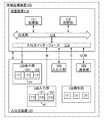
図1は本発明の一態様の情報処理装置の構成を説明するブロック図である。図2は本発明
の一態様の情報処理装置の記憶部が記憶するプログラムを説明するフロー図である。図3
は本発明の一態様の情報処理装置に用いることができる入力部の構成を説明するブロック
図および動作を説明するマップの模式図である。FIG. 1 is a block diagram illustrating a configuration of an information processing device of one embodiment of the present invention. FIG. 2 is a flowchart illustrating a program stored in the storage unit of the information processing apparatus according to one embodiment of the present invention. FIG.
These are a block diagram explaining the structure of the input part which can be used for the information processing apparatus of 1 aspect of this invention, and the schematic diagram of the map explaining operation | movement.
図2(A)は本発明の一態様のプログラムの主の部分を説明するフロー図であり、図2(
B)は割り込み処理を説明するフロー図であり、図2(C)は二次マップ生成処理を説明
するフロー図である。FIG. 2A is a flowchart for explaining a main part of the program of one embodiment of the present invention.
FIG. 2B is a flowchart illustrating interrupt processing, and FIG. 2C is a flowchart illustrating secondary map generation processing.
図3(A−1)は入力部の構成を説明するブロック図であり、図3(A−2)は入力部の
検知ユニットの構成を説明する回路図である。図3(D−1)および図3(D−2)は本
発明の一態様のプログラムの二値化マップを生成するステップと、ラベリングデータを生
成するステップを説明するための、マップの模式図である。FIG. 3A-1 is a block diagram illustrating the configuration of the input unit, and FIG. 3A-2 is a circuit diagram illustrating the configuration of the detection unit of the input unit. 3D-1 and 3D-2 are schematic diagrams of maps for explaining the steps of generating a binarized map of the program according to one embodiment of the present invention and the step of generating labeling data. It is.
<情報処理装置の構成例1.>
本実施の形態で説明する情報処理装置100は、マップMを供給する入力部140と、マ
ップMを供給される演算装置110と、を有する(図1参照)。<Configuration example 1 of information processing apparatus>>
The information processing apparatus 100 described in the present embodiment includes an
マップMは、背景マップMBKおよび一次マップM1を含む。The map M includes a background map MBK and a primary map M1.
演算装置110は、記憶部112と演算部111を備える。The calculation device 110 includes a
記憶部112は、マップMに基づいて所定の命令を供給するプログラムを記憶する。The
演算部111は、以下のステップを備えるプログラムを実行する。The
《第1のステップ》
第1のステップにおいて、割り込み処理を実行しパターンを抽出する(図2(A)(S1
)参照)。なお割り込み処理の詳細は第4のステップ乃至第9のステップにおいて説明す
る。<< First Step >>
In the first step, interrupt processing is executed to extract a pattern (FIG. 2 (A) (S1
)reference). The details of the interrupt process will be described in the fourth to ninth steps.
《第2のステップ》
第2のステップにおいて、パターンを参照テーブルと照合し、所定のパターンと一致する
場合に第3のステップに進み、所定のパターンと一致しない場合は第1のステップに進む
(図2(A)(S2)参照)。<< Second Step >>
In the second step, the pattern is checked against the reference table. If the pattern matches the predetermined pattern, the process proceeds to the third step. If the pattern does not match the predetermined pattern, the process proceeds to the first step (FIG. 2 (A) ( (See S2)).
これにより、情報処理装置100の使用者は、入力部140に近接または/および接触さ
せた指やスタイラス等を、所定のパターンを描くように移動して、入力部140にジェス
チャーを供給することができる。Accordingly, the user of the information processing apparatus 100 can supply a gesture to the
《第3のステップ》
第3のステップにおいて、所定のパターンに関連付けられた命令を供給し、第1のステッ
プに進む(図2(A)(S3)参照)。《Third step》
In the third step, an instruction associated with a predetermined pattern is supplied, and the process proceeds to the first step (see FIG. 2A and S3).
また、割り込み処理は以下のステップを具備する。The interrupt process includes the following steps.
《第4のステップ》
第4のステップにおいて、背景マップMBKおよび一次マップM1を取得し、背景マップ
MBKおよび一次マップM1に差がある場合は第5のステップに進み、差がない場合は割
り込み処理を終了する(図2(B)(T4)参照)。<< Fourth Step >>
In the fourth step, the background map MBK and the primary map M1 are acquired. If there is a difference between the background map MBK and the primary map M1, the process proceeds to the fifth step, and if there is no difference, the interrupt process is terminated (FIG. 2). (See (B) (T4)).
背景マップMBKは基準となるマップである。例えば、検出できる対象物が近接または/
および接触していない状態で、入力部140が供給する信号を、背景マップMBKに用い
ることができる。The background map MBK is a reference map. For example, a detectable object is close or /
In addition, the signal supplied by the
例えば、入力部140が背景マップMBKを取得した時間と異なる時間に取得したマップ
を、一次マップM1に用いることができる。具体的には、入力部140が所定の間隔で供
給するマップによって、逐次更新されるマップを、一次マップM1に用いることができる
。For example, a map acquired at a time different from the time when the
《第5のステップ》
第5のステップにおいて、背景マップMBKおよび一次マップM1に基づいて、二次マッ
プM2を生成する二次マップ生成処理を行う(図2(B)(T5)参照)。<< 5th step >>
In the fifth step, a secondary map generation process for generating the secondary map M2 is performed based on the background map MBK and the primary map M1 (see FIG. 2B (T5)).
なお、さまざまな方法を二次マップ生成処理に用いることができる。詳細は後に説明する
。Various methods can be used for the secondary map generation process. Details will be described later.
《第6のステップ》
第6のステップにおいて、二次マップM2に基づいて二値化マップMBIを生成する(図
2(B)(T6)参照)。<< Sixth Step >>
In the sixth step, a binarized map MBI is generated based on the secondary map M2 (see FIG. 2B and T6).
例えば、8行8列の二次マップM2を模式的に示す(図3(C−3)参照)。また、二次
マップM2を二値化して得た二値化マップMBIを模式的に示す(図3(D−1)参照)
。なお、セルの値の差異が可視化されるように、異なるハッチがセルの値に基づいて付さ
れている。For example, an 8-by-8 secondary map M2 is schematically shown (see FIG. 3C-3). In addition, a binarized map MBI obtained by binarizing the secondary map M2 is schematically shown (see FIG. 3D-1).
. Note that different hatches are added based on the cell values so that the difference in cell values is visualized.
マップの値を二値化する方法に様々な方法を用いることができる。例えば、8bitのデ
ータを用いる場合、各セルの値を0または255に二値化することができる。なお、二値
化をする際に用いる閾値を使用者が決定してもよいし、演算装置が決定してもよい。Various methods can be used for binarizing the map values. For example, when 8-bit data is used, the value of each cell can be binarized to 0 or 255. In addition, the user may determine the threshold value used when binarizing, or the arithmetic unit may determine.
《第7のステップ》
第7のステップにおいて、二値化マップMBIに基づいてラベリングデータLDを生成す
る(図2(B)(T7)参照)。<< Seventh Step >>
In the seventh step, labeling data LD is generated based on the binarization map MBI (see FIG. 2B and T7).
ラベリングをする方法に様々な方法を用いることができる。例えば、隣接するセルの値と
比較して同じ値である場合に同じラベルを付与するステップを、各セルについて行う(図
3(D−2)参照)。Various methods can be used for labeling. For example, the step of assigning the same label when the value is the same as the value of an adjacent cell is performed for each cell (see FIG. 3D-2).
これにより、同一のラベルが付された領域ごとに位置情報を特定することができる。例え
ば、同一のラベルが付された領域の重心を当該領域の位置情報とすることができる。Thereby, position information can be specified for each region to which the same label is attached. For example, the center of gravity of a region with the same label can be used as the position information of the region.
その結果、入力部140に近接または/および接触するものの検知情報と位置情報が関連
付けられたラベリングデータLDを生成することができる。As a result, it is possible to generate the labeling data LD in which the detection information and the position information that are close to and / or in contact with the
《第8のステップ》
第8のステップにおいて、ラベリングデータLDに基づいてデータセットを生成または更
新する(図2(B)(T8)参照)。<< Eighth Step >>
In the eighth step, a data set is generated or updated based on the labeling data LD (see FIG. 2B and T8).
《第9のステップ》
第9のステップにおいて、データセットに含まれるパターンを抽出する(図2(B)(T
9)参照)。<< Ninth Step >>
In the ninth step, patterns included in the data set are extracted (FIG. 2B (T
9)).
データセットは連続する複数のラベリングデータを含む。例えばラベリングデータLDの
時系列をデータセットに用いることができる。The data set includes a plurality of continuous labeling data. For example, a time series of labeling data LD can be used for the data set.
なお、ラベリングデータLDは、入力部140に近接または/および接触するものの検知
情報と位置情報が関連付けられたデータである。Note that the labeling data LD is data in which detection information and position information of what is close to and / or in contact with the
例えば、入力部140に近接または/および接触するものの数、位置、入力部140まで
の距離等をラベリングデータLDに含ませることができる。For example, the number, position, distance to the
このようなデータセットを用いると、入力部140に近接または/および接触するものの
移動に伴う軌跡を知り、そのパターンを抽出することができる。By using such a data set, it is possible to know the trajectory associated with the movement of the object close to and / or in contact with the
具体的には、およそ同じ場所をタップする指が描く軌跡、一方向にドラッグする指が描く
軌跡またはピンチする二つの指が間隔を広げながら描く軌跡などを抽出することができる
。なお、第9のステップを終えた後、割り込み処理を終了する。Specifically, a trajectory drawn by a finger tapping approximately the same place, a trajectory drawn by a finger dragging in one direction, or a trajectory drawn while increasing the interval between two fingers to be pinched can be extracted. Note that after completing the ninth step, the interrupt processing ends.
データセットは連続する複数のマップを含む。例えばマップの時系列をデータセットに用
いることができる。マップの時系列を含むデータセットを用いると、入力部140に近接
または/および接触するものの移動に伴う軌跡を知ることができる。The data set includes a plurality of consecutive maps. For example, a time series of maps can be used for the data set. By using a data set including a time series of maps, it is possible to know a trajectory associated with the movement of an object that approaches or / and contacts the
上記本発明の一態様の情報処理装置100は、マップMを供給する入力部140と、プロ
グラムを記憶する記憶部112と、を含んで構成される。また、プログラムは、マップM
からデータセットを生成する割り込み処理と、割り込み処理で生成されたデータセットか
らパターンを抽出するステップと、抽出されたパターンが参照テーブルに含まれる場合に
参照テーブルで関連付けられた命令を供給するステップと、を備える。The information processing apparatus 100 according to one aspect of the present invention includes the
An interrupt process for generating a data set from, a step of extracting a pattern from the data set generated by the interrupt process, and a step of supplying an instruction associated with the reference table when the extracted pattern is included in the reference table; .
なお、マップMは検知情報および検知した位置に係る位置情報を含むデータであり、デー
タセットは連続する複数のマップを含み、例えばマップの時系列をデータセットに用いる
ことができる。The map M is data including detection information and position information related to the detected position, and the data set includes a plurality of continuous maps. For example, a time series of maps can be used for the data set.
これにより、入力部140を用いて所定の命令を供給することができる。その結果、利便
性または信頼性に優れた新規な情報処理装置を提供することができる。または、新規な情
報処理装置を提供することができる。Accordingly, a predetermined command can be supplied using the
例えば、情報処理装置100の使用者は、入力部140に近接させた指や掌等を用いて、
様々な操作命令を情報処理装置100に供給することができる。For example, the user of the information processing apparatus 100 uses a finger, a palm, or the like brought close to the
Various operation commands can be supplied to the information processing apparatus 100.
例えば、終了命令(プログラムを終了する命令)を含む操作命令を供給することができる
。For example, an operation instruction including an end instruction (an instruction to end the program) can be supplied.
以下に、情報処理装置を構成する個々の要素について説明する。なお、これらの構成は明
確に分離できず、一つの構成が他の構成を兼ねる場合や他の構成の一部を含む場合がある
。Below, each element which comprises information processing apparatus is demonstrated. Note that these configurations cannot be clearly separated, and one configuration may serve as another configuration or may include a part of another configuration.
例えばタッチセンサが表示パネルに重ねられたタッチパネルは、表示部130であるとと
もに、入力部140でもある。For example, a touch panel in which a touch sensor is superimposed on a display panel is not only the display unit 130 but also the
なお、本実施の形態では表示部130の表示面側に入力部140が重ねられた構成を有す
るタッチセンサを例に説明するが、この構成に限られない。具体的には、入力部140の
検知面側に表示部130が重ねられた構成であってもよいし、表示部130と入力部14
0が一体の構造を有していてもよい。言い換えると、オン・セル型のタッチパネルであっ
てもイン・セル型のタッチパネルであってもよい。In the present embodiment, a touch sensor having a configuration in which the
0 may have an integral structure. In other words, it may be an on-cell type touch panel or an in-cell type touch panel.
《全体の構成》
情報処理装置100は、入出力装置120または演算装置110を有する(図1参照)。<Overall configuration>
The information processing apparatus 100 includes an input / output device 120 or an arithmetic device 110 (see FIG. 1).
《入出力装置120》
入出力装置120は、表示情報Vを供給され、マップMまたは検知情報Sを供給すること
ができる。また、演算装置110と入出力装置120は互いにさまざまな情報を供給し供
給されることができる。<< Input / output device 120 >>
The input / output device 120 is supplied with the display information V and can supply the map M or the detection information S. Further, the arithmetic device 110 and the input / output device 120 can supply and supply various information to each other.
入出力装置120は、表示部130、入力部140、入出力部145、検知部150また
は通信部160を有する。The input / output device 120 includes a display unit 130, an
《表示部130》
表示部130は、表示情報Vが供給され、表示情報Vを表示することができる。<< Display unit 130 >>
The display unit 130 is supplied with the display information V and can display the display information V.
表示部130は表示領域131を備え、表示情報Vを表示領域131に表示する。The display unit 130 includes a
表示領域131は、第1の表示領域131(11)、第1の屈曲できる表示領域131(
21)、第2の表示領域131(12)、第2の屈曲できる表示領域131(22)およ
び第3の表示領域131(13)を備えてもよい。The
21), a second display area 131 (12), a second bendable display area 131 (22), and a third display area 131 (13).
第1の屈曲できる表示領域131(21)および第2の屈曲できる表示領域131(22
)は、表示情報Vを表示することができるだけでなく屈曲することができる。The first bendable display area 131 (21) and the second bendable display area 131 (22)
) Can not only display the display information V but also bend it.
例えば、第1の屈曲できる表示領域131(21)および第2の屈曲できる表示領域13
1(22)は、10mm以下、好ましくは8mm以下、より好ましくは5mm以下、特に
好ましくは4mm以下の曲率半径で屈曲することができる。For example, the first bendable display area 131 (21) and the second
1 (22) can be bent with a radius of curvature of 10 mm or less, preferably 8 mm or less, more preferably 5 mm or less, and particularly preferably 4 mm or less.
表示部130は、第1の屈曲できる表示領域131(21)に第1の畳み目が形成される
ように折り畳むことができる。また、第1の畳み目を広げて表示部130を展開すること
ができる。The display unit 130 can be folded so that a first fold is formed in the first bendable display area 131 (21). Further, the display unit 130 can be expanded by expanding the first fold.
表示部130は、第2の屈曲できる表示領域131(22)に第2の畳み目が形成される
ように折り畳むことができる。また、第2の畳み目を広げて表示部130を展開すること
ができる。The display unit 130 can be folded so that a second fold is formed in the second bendable display region 131 (22). Further, the display unit 130 can be expanded by expanding the second fold.
第1の表示領域131(11)と第2の表示領域131(12)を、一体で駆動してもよ
い。例えば、一の走査線駆動回路が走査線を選択する信号を供給する構成としてもよい。The first display area 131 (11) and the second display area 131 (12) may be driven integrally. For example, one scanning line driving circuit may supply a signal for selecting a scanning line.
第1の表示領域131(11)と第2の表示領域131(12)を、別々に駆動してもよ
い。例えば、駆動回路をそれぞれの領域に設け、それぞれの走査線駆動回路がそれぞれの
走査線を選択する信号を供給する構成としてもよい。The first display area 131 (11) and the second display area 131 (12) may be driven separately. For example, a driving circuit may be provided in each region, and each scanning line driving circuit may supply a signal for selecting each scanning line.
例えば、情報処理装置100の待機状態において、第1の表示領域131(11)または
/および第1の屈曲できる表示領域131(21)のみを駆動して、他の領域の駆動を停
止してもよい。または、情報処理装置100の折り畳まれた状態において、第1の表示領
域131(11)または/および第1の屈曲できる表示領域131(21)のみを駆動し
て、他の視認できない領域の駆動を停止してもよい。他の領域の駆動を停止することによ
り、消費電力を低減することができる。For example, in the standby state of the information processing apparatus 100, even if only the first display area 131 (11) and / or the first bendable display area 131 (21) is driven and driving of other areas is stopped Good. Alternatively, in the folded state of the information processing apparatus 100, only the first display area 131 (11) and / or the first bendable display area 131 (21) is driven to drive other invisible areas. You may stop. Power consumption can be reduced by stopping driving in other regions.
《入力部140》
入力部140は、マップMを供給する。例えば、入力部140に近接または/および接触
するものを検知し、検知した情報を検知した位置に係る位置情報と関連付けて供給する。<
The
なお、マップMは検知情報および検知した位置に係る位置情報を含むデータである。また
、連続する複数のマップを含むデータをデータセットという。例えば、マップの時系列を
データセットに用いることができる。The map M is data including detection information and position information related to the detected position. Data including a plurality of continuous maps is called a data set. For example, a time series of maps can be used for the data set.
例えば、入力部140は、m行n列のマトリクス状に配置された複数の検知ユニットU(
m,n)を備える(図3(A−1)参照)。なお、mおよびnは自然数であり、mまたは
nの一方は2以上の自然数である。また、行方向に配設された複数の検知ユニットを電気
的に接続する第1の制御線等、列方向に配設された複数の検知ユニットを電気的に接続す
る信号線等を含むことができる。For example, the
m, n) (see FIG. 3A-1). Note that m and n are natural numbers, and one of m or n is a natural number of 2 or more. Further, it may include a signal line for electrically connecting a plurality of detection units arranged in the column direction, such as a first control line for electrically connecting a plurality of detection units arranged in the row direction. it can.
例えば、各検知ユニットU(m,n)が供給する検知信号と検知ユニットU(m,n)の
配置を関連付けたm行n列の行列を、マップMのデータの形式に用いることができる。具
体的には、m行n列の行列の要素(i,j)の値を、検知ユニットU(i,j)が供給す
る検知信号に基づく値とするデータの形式にしてもよい。なお、iはm以下の自然数であ
り,jはn以下の自然数である。For example, a matrix of m rows and n columns in which the detection signals supplied by the detection units U (m, n) and the arrangement of the detection units U (m, n) are associated can be used as the data format of the map M. Specifically, the value of the element (i, j) of the matrix of m rows and n columns may be in the form of data that is a value based on the detection signal supplied by the detection unit U (i, j). Note that i is a natural number of m or less, and j is a natural number of n or less.
なお、入力部140は、複数の検知ユニットU(m,n)、第1の制御線等またはこれら
を支持する基材を含むことができる。また、選択信号を供給することができる駆動回路ま
たは検知信号を供給することができる駆動回路等を含むことができる。Note that the
入力部140は、第1の入力部141(11)、第2の入力部141(12)、第3の入
力部141(13)第4の入力部141(21)および第5の入力部141(22)を備
える。The
入力部140は、表示部130と重なるように配置してもよい。The
具体的には、第1の表示領域131(11)に重ねて第1の入力部141(11)を、第
2の表示領域131(12)に重ねて第2の入力部141(12)を、第3の表示領域1
31(13)に重ねて第3の入力部141(13)を配置し、第1の屈曲できる表示領域
131(21)に重ねて屈曲することができる第4の入力部141(21)を配置する。
また、第2の屈曲できる表示領域131(22)に重ねて屈曲できる第5の入力部141
(22)を配置する。Specifically, the first input unit 141 (11) is overlaid on the first display region 131 (11), and the second input unit 141 (12) is overlaid on the second display region 131 (12). ,
3rd input part 141 (13) is arranged so that it may overlap with 31 (13), and 4th input part 141 (21) which can be bent over the display area 131 (21) which can be bent is arranged. To do.
Further, a
(22) is arranged.
なお、表示部130より使用者側に入力部140を配置する場合は、透光性を有する入力
部140を配置する。When the
第1の入力部141(11)は他の入力部と一体で駆動してもよいし、別々に駆動しても
よい。The first input unit 141 (11) may be driven integrally with other input units, or may be driven separately.
例えば、第1の入力部141(11)が消費する電力および第2の入力部141(12)
が消費する電力の合計が、第1の入力部141(11)が消費する電力より大きい場合、
情報処理装置100の待機状態において、第1の入力部141(11)のみを駆動して、
第2の入力部141(12)の駆動を停止してもよい。第2の入力部141(12)の駆
動を停止することにより、消費電力を低減することができる。For example, the power consumed by the first input unit 141 (11) and the second input unit 141 (12)
Is greater than the power consumed by the first input unit 141 (11),
In the standby state of the information processing apparatus 100, only the first input unit 141 (11) is driven,
The driving of the second input unit 141 (12) may be stopped. Power consumption can be reduced by stopping the driving of the second input unit 141 (12).
入力部に配設する検知素子は、近接または/および接触するもの(例えば指や掌)を検知
できるセンサであればよく、例えばコイル、磁気センサ、光電変換素子または/および一
方の電極が導電膜と電気的に接続された容量素子などを適用できる。なお、光電変換素子
を有する基板を光学式のタッチセンサと、容量素子をマトリクス状に有する基板を容量式
のタッチセンサと、いうことができる。The detection element disposed in the input unit may be any sensor that can detect proximity or / and contact (for example, a finger or palm). A capacitor element electrically connected to the capacitor can be used. Note that a substrate having photoelectric conversion elements can be referred to as an optical touch sensor, and a substrate having capacitor elements in a matrix can be referred to as a capacitive touch sensor.
《検知ユニットU(m,n)》
検知ユニットU(m,n)は、さまざまなものを検知する。例えば、近接または接触する
ものを検知して検知情報を供給する。例えば静電容量、照度、磁力、電波または圧力等を
検知して、検知した物理量に基づく情報を供給する。具体的には、容量素子、光電変換素
子、磁気検知素子、圧電素子または共振器等を検知素子に用いることができる。<< Detection unit U (m, n) >>
The detection unit U (m, n) detects various things. For example, the detection information is supplied by detecting the proximity or contact. For example, capacitance, illuminance, magnetic force, radio wave, pressure, or the like is detected, and information based on the detected physical quantity is supplied. Specifically, a capacitive element, a photoelectric conversion element, a magnetic sensing element, a piezoelectric element, a resonator, or the like can be used as the sensing element.
具体的には、大気中において、指などの大気より大きな誘電率を備えるものが導電膜に近
接すると、指と導電膜の間の静電容量が変化する。この静電容量の変化を検知して検知信
号を供給することができる。具体的には、導電膜および当該導電膜に一方の電極が接続さ
れた容量素子を用いることができる。静電容量の変化に伴い電荷の分配が引き起こされ、
容量素子の両端の電極の電圧が変化する。この電圧の変化を検知信号に用いることができ
る。Specifically, in the atmosphere, when an object such as a finger having a dielectric constant greater than that of the atmosphere approaches the conductive film, the capacitance between the finger and the conductive film changes. This change in capacitance can be detected and a detection signal can be supplied. Specifically, a conductive film and a capacitor in which one electrode is connected to the conductive film can be used. As the capacitance changes, charge distribution is caused,
The voltage of the electrodes at both ends of the capacitive element changes. This change in voltage can be used as a detection signal.
また、入力部140が、マトリクス状に配置された複数の検知ユニットUと、行方向に配
設される複数の検知ユニットUと電気的に接続される第1の制御線G1と、列方向に配設
される複数の検知ユニットUと電気的に接続される信号線DLと、を有する場合、例えば
、以下の構成を備える検知ユニットUを用いることができる。The
検知ユニットUは、制御端子が第1の制御線G1に電気的に接続され、第1の端子が信号
線DLに電気的に接続される第1のスイッチSW1を備える。The detection unit U includes a first switch SW1 whose control terminal is electrically connected to the first control line G1, and whose first terminal is electrically connected to the signal line DL.
また、第1の電極が第1のスイッチSW1の第2の端子に電気的に接続され、第2の電極
が第1の電源線VPIと電気的に接続される増幅トランジスタM10を備える。Further, the amplifier includes an amplification transistor M10 in which the first electrode is electrically connected to the second terminal of the first switch SW1, and the second electrode is electrically connected to the first power supply line VPI.
また、第1の電極が増幅トランジスタM10のゲートおよび導電膜と電気的に接続され、
第2の電極が第2の制御線CSと電気的に接続される容量素子C1を備える。なお、増幅
トランジスタM10のゲート、容量素子C1の第2の電極および導電膜が電気的に接続さ
れるノードをノードAとする。増幅トランジスタM10はノードAの電位に基づく大きさ
の電流を第1の電極と第2の電極の間に流す。これにより、例えば、信号線DLを流れる
電流に基づく情報を供給する回路を用いて、検知ユニットが供給する検知信号に基づく検
知情報を供給することができる。Further, the first electrode is electrically connected to the gate and the conductive film of the amplification transistor M10,
The second electrode includes a capacitor C1 that is electrically connected to the second control line CS. Note that a node to which the gate of the amplification transistor M10, the second electrode of the capacitor C1, and the conductive film are electrically connected is referred to as a node A. The amplification transistor M10 passes a current having a magnitude based on the potential of the node A between the first electrode and the second electrode. Thereby, for example, detection information based on the detection signal supplied by the detection unit can be supplied using a circuit that supplies information based on the current flowing through the signal line DL.
第1の端子が増幅トランジスタM10のゲートと電気的に接続され、制御端子が第3の制
御線RESと電気的に接続され、第2の端子が第2の電源線VRESと電気的に接続され
る第2のスイッチSW2を備える。The first terminal is electrically connected to the gate of the amplification transistor M10, the control terminal is electrically connected to the third control line RES, and the second terminal is electrically connected to the second power supply line VRES. A second switch SW2.
《検知部150》
検知部150は、情報処理装置100または/およびその周囲の状態を検知して検知情報
Sを供給することができる(図1参照)。<< Detector 150 >>
The detection unit 150 can detect the information processing apparatus 100 and / or its surrounding state and supply the detection information S (see FIG. 1).
検知部150は、入出力装置120が折り畳まれた状態かまたは展開された状態かを検知
し、入出力装置120の折り畳まれた状態または展開された状態を示す情報を含む検知情
報Sを供給する。具体的には、表示部130または/および入力部140が折り畳まれた
状態かまたは展開された状態かを検知する。The detection unit 150 detects whether the input / output device 120 is folded or unfolded, and supplies detection information S including information indicating the folded state or the unfolded state of the input / output device 120. . Specifically, it is detected whether the display unit 130 and / or the
入出力装置120の折り畳まれた状態または展開された状態は、各種のセンサを用いて検
知することができる。The folded or unfolded state of the input / output device 120 can be detected using various sensors.
例えば、メカニカルスイッチ、光学式スイッチ、磁気センサ、光電変換素子、MEMS圧
力センサまたは感圧センサ等を用いて入出力装置120の折り畳まれた状態を検知するこ
とができる。For example, the folded state of the input / output device 120 can be detected using a mechanical switch, an optical switch, a magnetic sensor, a photoelectric conversion element, a MEMS pressure sensor, a pressure sensor, or the like.
例えば、第2の表示領域131(12)または第3の表示領域131(13)の表示を遮
るものを検知して、表示部130の折り畳まれた状態を検知することができる。For example, it is possible to detect the folded state of the display unit 130 by detecting an object that blocks the display of the second display area 131 (12) or the third display area 131 (13).
具体的には、情報処理装置100に光電変換素子を、第2の表示領域131(12)に表
示される表示情報Vを入出力装置が折り畳まれた状態で検知するように配置し、当該光電
変換素子を用いて第3の表示領域131(13)を検知して、表示部130が第2の屈曲
できる表示領域131(22)で折り畳まれたか否かを検知することができる。Specifically, the photoelectric conversion element is arranged in the information processing apparatus 100 so as to detect the display information V displayed in the second display region 131 (12) in a state where the input / output device is folded, and The third display area 131 (13) can be detected using the conversion element, and it can be detected whether the display unit 130 is folded in the second bendable display area 131 (22).
なお、検知部150は、例えば加速度、角加速度、方位、圧力、GPS(Global
positioning System)信号、温度または湿度等を検知して、その情報
を供給してもよい。In addition, the detection part 150 is, for example, acceleration, angular acceleration, azimuth, pressure, GPS (Global
(positioning system) signal, temperature or humidity may be detected and the information may be supplied.
《通信部160》
通信部160は、通信情報COMを供給し供給される。通信部160は、演算装置110
が供給する情報COMを情報処理装置100の外部の機器または通信網に供給する。また
、情報COMを外部の機器または通信網から取得して供給する。<<
The
Supplies the information COM supplied to the device outside the information processing apparatus 100 or a communication network. Information COM is acquired from an external device or a communication network and supplied.
情報COMは、音声情報、画像情報等の他、様々な命令等を含むことができる。例えば、
表示情報Vを演算部111に生成または消去等させる操作命令を含むことができる。The information COM can include various instructions in addition to audio information, image information, and the like. For example,
An operation command for causing the
外部の機器または通信網に接続するための通信手段、例えばハブ、ルータまたはモデム等
を通信部160に適用できる。なお、接続方法は有線による方法に限らず、無線(例えば
電波または赤外線等)をもちいてもよい。A communication means for connecting to an external device or a communication network, such as a hub, a router, or a modem, can be applied to the
《入出力部145》
入出力部145は、さまざまな情報を供給し供給される。例えば、カメラ、マイク、読み
取り専用の外部記憶部、外部記憶部、スキャナー、スピーカまたはプリンタ等を入出力部
145に用いることができる。<< Input /
The input /
具体的には、デジタルカメラおよびデジタルビデオカメラ等をカメラに用いることができ
る。Specifically, a digital camera, a digital video camera, or the like can be used for the camera.
ハードディスクまたはリムーバブルメモリなどを外部記憶部に用いることができる。また
、CDROM、DVDROM等を読み取り専用の外部記憶部に用いることができる。A hard disk or a removable memory can be used for the external storage unit. Also, CDROM, DVDROM, etc. can be used as a read-only external storage unit.
《演算装置110》
演算装置110は、演算部111または記憶部112を備える。演算装置110は表示情
報Vを供給し、マップMまたは検知情報Sを供給される(図1参照)。<< Calculation device 110 >>
The computing device 110 includes a
例えば、演算装置110は、情報処理装置100の操作の用に供する画像を含む表示情報
Vを供給する。For example, the arithmetic device 110 supplies display information V including an image used for the operation of the information processing device 100.
また、演算装置110は、マップMを供給されてもよい。In addition, the arithmetic device 110 may be supplied with the map M.
例えば、表示部130に表示された操作の用に供する画像に重なる部分の入力部140を
指等で触れることにより、使用者は当該画像に関連付けられた操作命令を演算装置110
に供給できる。For example, when the user touches a part of the
Can supply.
また、演算装置110は、伝送路114と、入出力インターフェース115を有していて
もよい。Further, the arithmetic device 110 may have a
《演算部111》
演算部111は、記憶部112が記憶するプログラムを実行する。例えば、操作の用に供
する画像を表示した位置の位置情報Lが供給された場合に、演算部111は当該画像にあ
らかじめ関連付けられたプログラムを実行する。<<
The
《記憶部112》
記憶部112は、演算部111に実行させるプログラムを記憶する。<<
The
《入出力インターフェース・伝送路》
入出力インターフェース115は情報を供給し、情報が供給される。<Input / output interface and transmission path>
The input / output interface 115 supplies information and information is supplied.
伝送路114は情報を供給することができ、演算部111、記憶部112および入出力イ
ンターフェース115は情報を供給される。また、演算部111、記憶部112および入
出力インターフェース115は、情報を供給することができ、伝送路114は情報を供給
される。The
《筐体》
情報処理装置100は筐体を有していてもよい。筐体は、情報処理装置100に加わるさ
まざまな応力から演算装置110等を保護することができる。<Case>
The information processing apparatus 100 may have a housing. The housing can protect the arithmetic device 110 and the like from various stresses applied to the information processing apparatus 100.
金属、プラスチック、ガラスまたはセラミックス等を筐体に用いることができる。Metal, plastic, glass, ceramics, or the like can be used for the housing.
<情報処理装置の構成例2.>
本発明の一態様の情報処理装置の別の構成について、図2(C)および図3を参照しなが
ら説明する。<Configuration example 2 of information processing apparatus>>
Another structure of the information processing device of one embodiment of the present invention is described with reference to FIGS.
図2(C)は本発明の一態様の情報処理装置の記憶部が記憶するプログラムを説明するフ
ロー図である。FIG. 2C is a flowchart illustrating a program stored in the storage unit of the information processing device of one embodiment of the present invention.
図3(A−1)は本発明の一態様の情報処理装置の入力部140のブロック図であり、図
3(A−2)は入力部140に用いることができる検知ユニットの構成を説明する回路図
である。図3(B)乃至図3(D−2)は入力部140が供給するマップを説明するため
の模式図である。3A-1 is a block diagram of the
本実施の形態で説明する情報処理装置100の構成例2は、記憶部112が以下のステッ
プを備える二次マップ生成処理をするためのプログラムを記憶する点が、上記で説明する
情報処理装置100の構成例1と異なる。ここでは異なる構成について詳細に説明し、同
様の構成を用いることができる部分は、上記の説明を援用する。In the configuration example 2 of the information processing apparatus 100 described in the present embodiment, the information processing apparatus 100 described above is that the
演算部111は、記憶部112が記憶する以下のステップを備えるプログラムを実行する
。The
《第10のステップ》
第10のステップにおいて、一次マップM1から背景マップMBKを差し引く(図2(C
)(U10)参照)。<< Tenth Step >>
In the tenth step, the background map MBK is subtracted from the primary map M1 (FIG. 2 (C
) (See U10)).
背景マップMBKの模式図を示す(図3(B)参照)。なお、図示する背景マップは8行
8列のものであるが、これに限られない。また、異なる値のセルには異なるハッチが付さ
れている。A schematic diagram of the background map MBK is shown (see FIG. 3B). Although the illustrated background map is of 8 rows and 8 columns, it is not limited to this. Different cells are given different hatches.
一次マップM1の模式図を示す(図3(C−1)参照)。なお、図示する一次マップM1
は8行8列のものであるが、これに限られない。例えば、入力部140が検知できるもの
が近接または/および接触している状態で、入力部140が供給する信号を、一次マップ
に用いることができる。A schematic diagram of the primary map M1 is shown (see FIG. 3C-1). The primary map M1 shown in the figure
Is of 8 rows and 8 columns, but is not limited to this. For example, a signal supplied by the
一次マップM1を背景マップMBKと比較する。具体的には、一次マップM1から背景マ
ップMBKを差し引く。これにより、入力部140に近接または/および接触するものに
係る情報を取得できる。例えば、入力部140に近接または/および接触するものの数、
位置または入力部までの距離等を知ることができる(図3(C−2)参照)。The primary map M1 is compared with the background map MBK. Specifically, the background map MBK is subtracted from the primary map M1. As a result, information related to what is close to and / or in contact with the
The position or the distance to the input unit can be known (see FIG. 3C-2).
《第11のステップ》
第11のステップにおいて、第10のステップで得た結果に一様な値を加え、嵩上げされ
たマップを生成する(図2(C)(U11)参照)。<Eleventh step>
In the eleventh step, a uniform value is added to the result obtained in the tenth step to generate a raised map (see FIG. 2C (U11)).
例えば、同じ値を各セルに加える。具体的には、8bitの信号を用いる場合、中央の値
127を各セルに加えてもよい(図3(C−3)参照)。For example, add the same value to each cell. Specifically, when an 8-bit signal is used, a central value 127 may be added to each cell (see FIG. 3 (C-3)).
《第12のステップ》
第12のステップにおいて、嵩上げされたマップに含まれる上限値を超える値を上限値に
変換し、下限値を下回る値を下限値に変換する(図2(C)(U12)参照)。なお、こ
のマップが二次マップM2になる。また、第12のステップを終えたのち、二次マップ生
成処理を終了する。<< Twelfth Step >>
In the twelfth step, a value exceeding the upper limit value included in the raised map is converted into an upper limit value, and a value lower than the lower limit value is converted into a lower limit value (see FIG. 2C (U12)). This map becomes the secondary map M2. Moreover, after finishing the twelfth step, the secondary map generation process is terminated.
具体的には、8bitの信号を用いる場合、255より大きい値は255に変換し、0よ
り小さい値は0に変換する。Specifically, when an 8-bit signal is used, a value larger than 255 is converted to 255, and a value smaller than 0 is converted to 0.
本実施の形態で説明する情報処理装置100の構成例2は、記憶部112を含み、当該記
憶部112が一次マップM1から背景マップMBKを差し引くステップを備えるプログラ
ムを記憶する。Configuration example 2 of the information processing apparatus 100 described in the present embodiment includes a
なお、使用者に使用されていない状態の入力部140が供給するマップを背景マップMB
Kに用いることができる。Note that the map supplied by the
Can be used for K.
これにより、入力部が供給するマップから雑音を取り除くことができる。また、雑音が取
り除かれたマップを用いて所定の命令を供給することができる。その結果、利便性または
信頼性に優れた新規な情報処理装置を提供することができる。または、新規な情報処理装
置を提供することができる。Thereby, noise can be removed from the map supplied by the input unit. In addition, a predetermined command can be supplied using the map from which noise is removed. As a result, a novel information processing apparatus that is highly convenient or reliable can be provided. Alternatively, a novel information processing device can be provided.
<情報処理装置の構成例3.>
本発明の一態様の情報処理装置の別の構成について、図4を参照しながら説明する。<Configuration example 3 of information processing apparatus>>
Another structure of the information processing device of one embodiment of the present invention is described with reference to FIG.
図4は本発明の一態様のプログラムの主の部分の変形例を説明するフロー図である。FIG. 4 is a flowchart illustrating a modification of the main part of the program of one embodiment of the present invention.
本実施の形態で説明する情報処理装置100の構成例3は、記憶部112が、以下の第1
3のステップ乃至第15のステップを備えるプログラムを第3のステップに替えて記憶す
る点が、上記で説明する情報処理装置100の構成例1または構成例2と異なる。ここで
は異なる構成について詳細に説明し、同様の構成を用いることができる部分は、上記の説
明を援用する。In the configuration example 3 of the information processing apparatus 100 described in the present embodiment, the
The point which memorize | stores the program provided with 3 steps thru | or a 15th step instead of a 3rd step differs from the structural example 1 or the structural example 2 of the information processing apparatus 100 demonstrated above. Here, the different configurations will be described in detail, and the above description is used for portions where the same configurations can be used.
演算部111は、記憶部112が記憶する以下のステップを備えるプログラムを実行する
。The
《第13のステップ》
第13のステップにおいて、第2のステップで一致した所定のパターンに関連付けられた
命令を供給する。<< 13th Step >>
In a thirteenth step, an instruction associated with the predetermined pattern matched in the second step is supplied.
《第14のステップ》
第14のステップにおいて、背景マップMBKを生成する。<< 14th Step >>
In the fourteenth step, a background map MBK is generated.
例えば、入力部140が表示部130に重ねて設けられている場合、入力部140が表示
部130の動作状態の影響を受ける場合がある。具体的には、表示部130の表示素子の
動作が、入力部140の検知素子の動作に影響を与える場合がある。これにより、背景マ
ップMBKが表示情報Vの影響を受けて変化する場合がある。For example, when the
例えば、背景マップMBKが表示情報Vの影響を受けて変化する場合、表示情報Vの変化
に基づいて背景マップMBKを生成しなおしてもよい。具体的には、表示情報Vが第13
のステップにおいて供給した命令に基づいて供給された後に、一次マップM1を取得する
。そして、取得した一次マップM1を用いて背景マップMBKを生成してもよい。For example, when the background map MBK changes under the influence of the display information V, the background map MBK may be regenerated based on the change of the display information V. Specifically, the display information V is 13th.
After being supplied based on the instruction supplied in step (1), the primary map M1 is acquired. Then, the background map MBK may be generated using the acquired primary map M1.
《第15のステップ》
第15のステップにおいて、生成された背景マップMBKで背景マップを更新し、第1の
ステップに進む。<< 15th step >>
In the fifteenth step, the background map is updated with the generated background map MBK, and the process proceeds to the first step.
これにより、例えば入力部140が表示部130に重ねて配置されることにより、背景マ
ップMBKが表示情報Vに影響を受ける場合であっても、当該影響が加味された背景マッ
プMBKを新たに生成することができる。その結果、当該背景マップMBKを用いて、表
示情報Vに起因する影響を相殺することができる。Thereby, for example, even when the background map MBK is influenced by the display information V by arranging the
本実施の形態で説明する情報処理装置100の構成例2は、記憶部112を含み、当該記
憶部112は、背景マップMBKを生成するステップと、背景マップMBKを更新するス
テップと、を備えるプログラムを記憶する。Configuration example 2 of information processing apparatus 100 described in the present embodiment includes a
これにより、入力部の状態に基づいた背景マップを更新することができる。その結果、利
便性または信頼性に優れた新規な情報処理装置を提供することができる。または、新規な
情報処理装置を提供することができる。Thereby, the background map based on the state of the input unit can be updated. As a result, a novel information processing apparatus that is highly convenient or reliable can be provided. Alternatively, a novel information processing device can be provided.
なお、本実施の形態は、本明細書で示す他の実施の形態と適宜組み合わせることができる
。Note that this embodiment can be combined with any of the other embodiments described in this specification as appropriate.
(実施の形態2)
本実施の形態では、本発明の一態様の情報処理装置に用いることができる入出力装置の構
成について、図5および図6を参照しながら説明する。(Embodiment 2)
In this embodiment, structures of input / output devices that can be used for the information processing device of one embodiment of the present invention are described with reference to FIGS.
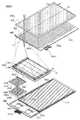
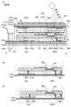
図5は本発明の一態様の入出力装置500TPの構成を説明する投影図である。なお、説
明の便宜のために検知ユニット602の一部および画素502の一部を拡大して図示して
いる。FIG. 5 is a projection view illustrating a structure of the input / output device 500TP of one embodiment of the present invention. For convenience of explanation, a part of the
図6(A)は図5に示す本発明の一態様の入出力装置500TPの切断線Z1−Z2にお
ける断面の構造を示す断面図であり、図6(B)および図6(C)は図6(A)に示す構
造の一部を置換することができる構造の変形例を示す断面図である。6A is a cross-sectional view illustrating a cross-sectional structure along the cutting line Z1-Z2 of the input / output device 500TP of one embodiment of the present invention illustrated in FIG. 5, and FIGS. 6B and 6C are diagrams. It is sectional drawing which shows the modification of the structure which can substitute a part of structure shown to 6 (A).
<入出力装置の構成例>
本実施の形態で説明する入出力装置500TPは、表示部500および表示部500に重
なる領域を備える入力部600を有する(図5参照)。<Configuration example of input / output device>
The input / output device 500TP described in this embodiment includes a
入力部600は、マトリクス状に配設される複数の検知ユニット602を有する。The
また、行方向(図中に矢印Rで示す)に配置される複数の検知ユニット602が電気的に
接続される第1の制御線G1または制御線RESなどを有する。In addition, the plurality of
また、列方向(図中に矢印Cで示す)に配置される複数の検知ユニット602が電気的に
接続される信号線DLなどを有する。In addition, a plurality of
検知ユニット602は検知回路を備える。検知回路は、第1の制御線G1、制御線RES
または信号線DLなどに電気的に接続される。The
Alternatively, it is electrically connected to the signal line DL or the like.
トランジスタまたは/および検知素子等を検知回路に用いることができる。例えば、導電
膜と、当該導電膜に電気的に接続される容量素子と、を検知素子に用いることができる。
また、容量素子と、当該容量素子に電気的に接続されるトランジスタと、を用いることが
できる。A transistor or / and a sensing element or the like can be used for the sensing circuit. For example, a conductive film and a capacitor electrically connected to the conductive film can be used for the detection element.
Further, a capacitor and a transistor electrically connected to the capacitor can be used.
容量素子650を検知回路に用いることができる。また、絶縁層653、絶縁層653を
挟持する第1の電極651および第2の電極652を容量素子650に用いることができ
る(図6(A)参照)。The
また、検知ユニット602はマトリクス状に配置された複数の窓部667を有する。窓部
667は可視光を透過し、遮光性の層BMを複数の窓部667の間に配設してもよい。The
窓部667に重なる領域を備える着色層を有する。着色層は、所定の色の光を透過する。
例えば、青色の光を透過する着色層CFB、緑色の光を透過する着色層CFGまたは赤色
の光を透過する着色層CFRを用いることができる。また、黄色の光を透過する着色層や
白色の光を透過する着色層を用いてもよい。なお、着色層をカラーフィルタということが
できる。A colored layer including a region overlapping with the
For example, a colored layer CFB that transmits blue light, a colored layer CFG that transmits green light, or a colored layer CFR that transmits red light can be used. Alternatively, a colored layer that transmits yellow light or a colored layer that transmits white light may be used. Note that the colored layer can be referred to as a color filter.
表示部500は、マトリクス状に配置された複数の画素502を有する。画素502は入
力部600の窓部667と重なる領域を備えるように配置されている。The
画素502は、検知ユニット602に比べて高い精細度で配設されてもよい。The
本実施の形態で説明する入出力装置500TPは、可視光を透過する窓部667を具備し
、マトリクス状に配設される複数の検知ユニット602を備える入力部600と、窓部6
67に重なる画素502を複数備える表示部500と、を有し、窓部667と画素502
の間に着色層を含んで構成される。また、それぞれの検知ユニットに他の検知ユニットへ
の電気的な干渉を低減することができるスイッチが配設されている。なお、トランジスタ
等をスイッチに用いることができる。The input / output device 500TP described in this embodiment includes a
67, a
It is comprised including a colored layer between. Each detection unit is provided with a switch that can reduce electrical interference to other detection units. Note that a transistor or the like can be used for the switch.
これにより、各検知ユニットが検知する検知情報を検知ユニットの位置情報と共に供給す
ることができる。また、画像を表示する画素の位置情報に関連付けて、検知情報を供給す
ることができる。また、検知情報を供給させない検知ユニットと信号線を非導通状態にす
ることで、検知信号を供給させる検知ユニットへの電気的な干渉を低減することができる
。その結果、利便性または信頼性に優れた新規な入出力装置500TPを提供することが
できる。Thereby, the detection information which each detection unit detects can be supplied with the positional information on a detection unit. In addition, detection information can be supplied in association with position information of a pixel displaying an image. In addition, by making the detection unit that does not supply detection information and the signal line non-conductive, electrical interference to the detection unit that supplies the detection signal can be reduced. As a result, a novel input / output device 500TP that is highly convenient or reliable can be provided.
例えば、入出力装置500TPの入力部600は検知情報を検知して位置情報と共に供給
することができる。具体的には、入出力装置500TPの使用者は、入力部600に触れ
た指等をポインタに用いて様々なジェスチャー(タップ、ドラッグ、スワイプまたはピン
チイン等)をすることができる。For example, the
入力部600は、入力部600に近接または接触する指等を検知して、検知した位置また
は軌跡等を含む検知情報を供給することができる。The
演算装置は供給された情報が所定の条件を満たすか否かをプログラム等に基づいて判断し
、所定のジェスチャーに関連付けられた命令を実行する。The arithmetic device determines whether the supplied information satisfies a predetermined condition based on a program or the like, and executes a command associated with a predetermined gesture.
これにより、入力部600の使用者は、指等を用いて所定のジェスチャーを供給し、所定
のジェスチャーに関連付けられた命令を演算装置に実行させることができる。Thereby, the user of the
例えば、入出力装置500TPの入力部600は、一の信号線に検知情報を供給すること
ができる複数の検知ユニットから一の検知ユニットを選択し、選択された検知ユニットを
除いた他の検知ユニットと当該一の信号線を非導通状態にすることができる。これにより
、選択されていない他の検知ユニットがもたらす選択された検知ユニットへの干渉を低減
することができる。For example, the
具体的には、選択されていない検知ユニットの検知素子がもたらす選択された検知ユニッ
トの検知素子への干渉を低減できる。Specifically, the interference of the selected detection unit to the detection element caused by the detection element of the unselected detection unit can be reduced.
例えば、容量素子および当該容量素子の一の電極が電気的に接続された導電膜を検知素子
に用いる場合において、選択されていない検知ユニットの導電膜の電位がもたらす、選択
された検知ユニットの導電膜の電位への干渉を低減することができる。具体的には、雑音
の低減に寄与することができる。For example, when a conductive film in which a capacitor element and one electrode of the capacitor element are electrically connected is used as a detection element, the conductivity of the selected detection unit is caused by the potential of the conductive film of an unselected detection unit. Interference with the membrane potential can be reduced. Specifically, it can contribute to noise reduction.
これにより、入出力装置500TPはその大きさに依存することなく、検知ユニットを駆
動して、検知情報を供給させることができる。例えば、ハンドヘルド型に用いることがで
きる大きさから、電子黒板に用いることができる大きさまで、さまざまな大きさの入出力
装置500TPを提供することができる。Accordingly, the input / output device 500TP can drive the detection unit and supply detection information without depending on the size of the input / output device 500TP. For example, the input / output device 500TP of various sizes can be provided from a size that can be used for a handheld type to a size that can be used for an electronic blackboard.
また、入出力装置500TPが折り畳まれた状態および展開された状態にすることができ
、且つ選択されていない検知ユニットが選択された検知ユニットにもたらす電気的な干渉
が、折り畳まれた状態と展開された状態とで異なる場合においても、入出力装置500T
Pの折り畳まれた状態または展開された状態に依存することなく検知ユニットを駆動して
、検知情報を供給させることができる。Further, the input / output device 500TP can be folded and unfolded, and electrical interference caused by the unselected detection unit to the selected detection unit is unfolded and unfolded. The input / output device 500T is different even when
The detection unit can be driven to supply detection information without depending on the folded state or the unfolded state of P.
また、入出力装置500TPの表示部500は表示情報Vを供給されることができる。例
えば、演算装置は表示情報Vを供給することができる。The
以上の構成に加えて、入出力装置500TPは以下の構成を備えることもできる。In addition to the above configuration, the input / output device 500TP may have the following configuration.
入出力装置500TPの入力部600は、駆動回路603gまたは駆動回路603dを備
えることができる。また、フレキシブルプリント基板FPC1を電気的に接続することが
できる。The
入出力装置500TPの表示部500は、信号線駆動回路503s、配線511または端
子519を備えてもよい。また、フレキシブルプリント基板FPC2と電気的に接続され
てもよい。The
また、使用に伴う傷の発生から入出力装置500TPを保護する機能を備える保護層67
0を備えることができる。例えば、セラミックコート層またはハードコート層を保護層6
70に用いることができる。具体的には、酸化アルミニウムを含む層またはUV硬化樹脂
等を含む層を用いることができる。また、入出力装置500TPが反射する外光の強度を
弱める機能を備える反射防止層670pを用いることができる。具体的には、円偏光板等
を用いることができる。Further, the protective layer 67 having a function of protecting the input / output device 500TP from generation of scratches due to use.
0 can be provided. For example, the ceramic coat layer or the hard coat layer is replaced with the protective layer 6.
70. Specifically, a layer containing aluminum oxide or a layer containing UV curable resin or the like can be used. The
以下に、入出力装置500TPを構成する個々の要素について説明する。なお、これらの
構成は明確に分離できず、一つの構成が他の構成を兼ねる場合や他の構成の一部を含む場
合がある。Hereinafter, individual elements constituting the input / output device 500TP will be described. Note that these configurations cannot be clearly separated, and one configuration may serve as another configuration or may include a part of another configuration.
例えば、複数の窓部667に重なる位置に着色層を備える入力部600は、入力部600
であるとともにカラーフィルタでもある。For example, the
It is also a color filter.
また、例えば入力部600が表示部500に重ねられた入出力装置500TPは、入力部
600であるとともに表示部500でもある。なお、表示部500に入力部600が重ね
られた入出力装置500TPをタッチパネルともいう。For example, the input / output device 500TP in which the
《全体の構成》
本実施の形態で説明する入出力装置500TPは、入力部600または表示部500を有
する。<Overall configuration>
The input / output device 500TP described in this embodiment includes an
なお、例えば実施の形態3乃至実施の形態5において説明する作製方法を用いて、入出力
装置500TPを作製することができる。Note that the input / output device 500TP can be manufactured using a manufacturing method described in
《入力部》
入力部600は、検知ユニット602、第1の制御線G1、信号線DLまたは基材610
を備える。<Input section>
The
Is provided.
例えば、入力部600を形成するための膜を基材610に成膜し、当該膜を加工して、入
力部600を形成することができる。For example, the
または、入力部600の一部を他の基材に形成し、当該一部を基材610に転置する方法
を用いて、入力部600を形成してもよい。Alternatively, the
《検知ユニット》
検知ユニット602は近接または接触するものを検知して検知信号を供給する。例えば静
電容量、照度、磁力、電波または圧力等を検知して、検知した物理量に基づく情報を供給
する。具体的には、容量素子、光電変換素子、磁気検知素子、圧電素子または共振器等を
検知素子に用いることができる。<Detection unit>
The
検知ユニット602は、検知素子および検知回路を備える。例えば、近接または接触する
ものとの間の静電容量の変化を検知する検知素子と検知回路を用いることができる。具体
的には、導電膜および導電膜と電気的に接続された検知回路を、検知ユニット602に用
いることができる。The
なお、大気中において、指などの大気より大きな誘電率を備えるものが導電膜に近接する
と、指と導電膜の間の静電容量が変化する。この静電容量の変化を検知して検知情報を供
給することができる。具体的には、導電膜および当該導電膜に一方の電極が接続された容
量素子を含む検知回路を検知ユニット602に用いることができる。In the atmosphere, when an object having a dielectric constant greater than that of the atmosphere, such as a finger, approaches the conductive film, the capacitance between the finger and the conductive film changes. Detection information can be supplied by detecting the change in capacitance. Specifically, a detection circuit including a conductive film and a capacitor in which one electrode is connected to the conductive film can be used for the
例えば、静電容量の変化に伴い容量素子との間で電荷の分配が引き起こされ、容量素子の
両端の電極の電圧が変化する。この電圧の変化を検知信号に用いることができる。具体的
には、容量素子650の一方の電極に電気的に接続された導電膜にものが近接することに
より、容量素子650の電極間の電圧は変化する(図6(A)参照)。For example, with the change in capacitance, charge is distributed with the capacitive element, and the voltage at the electrodes at both ends of the capacitive element changes. This change in voltage can be used as a detection signal. Specifically, the voltage between the electrodes of the
《スイッチ、トランジスタ》
検知ユニット602は、制御信号に基づいて導通状態または非導通状態にすることができ
るスイッチを備える。例えば、トランジスタM12をスイッチに用いることができる。《Switch, transistor》
The
また、検知信号を増幅するトランジスタを検知ユニット602に用いることができる。A transistor that amplifies the detection signal can be used for the
同一の工程で作製することができるトランジスタを、検知信号を増幅するトランジスタお
よびスイッチに用いることができる。これにより、作製工程が簡略化された入力部600
を提供できる。Transistors that can be manufactured in the same process can be used for transistors and switches that amplify a detection signal. Thereby, the
Can provide.
トランジスタは半導体層を備える。例えば、4族の元素、化合物半導体または酸化物半導
体を半導体層に用いることができる。具体的には、シリコンを含む半導体、ガリウムヒ素
を含む半導体またはインジウムを含む酸化物半導体などを半導体層に適用できる。また、
有機半導体などを半導体層に用いることができる。テトラセンやペンタセンなどのアセン
類、オリゴチオフェン誘導体、フタロシアニン類、ペリレン誘導体、ルブレン、Alq3
、TTF−TCNQ、ポリチオフェン(ポリ(3−ヘキシルチオフェン)(P3HT)な
ど)、ポリアセチレン、ポリフルオレン、ポリフェニレンビニレン、ポリピロール、ポリ
アニリン、アントラセン、テトラシアノキノジメタン (TCNQ)、ポリパラフェニレ
ンビニレン(PPV)などを有機半導体に用いることができる。The transistor includes a semiconductor layer. For example, a Group 4 element, a compound semiconductor, or an oxide semiconductor can be used for the semiconductor layer. Specifically, a semiconductor containing silicon, a semiconductor containing gallium arsenide, an oxide semiconductor containing indium, or the like can be used for the semiconductor layer. Also,
An organic semiconductor or the like can be used for the semiconductor layer. Acenes such as tetracene and pentacene, oligothiophene derivatives, phthalocyanines, perylene derivatives, rubrene, Alq3
, TTF-TCNQ, polythiophene (poly (3-hexylthiophene) (P3HT), etc.), polyacetylene, polyfluorene, polyphenylene vinylene, polypyrrole, polyaniline, anthracene, tetracyanoquinodimethane (TCNQ), polyparaphenylene vinylene (PPV) Can be used for organic semiconductors.
様々な結晶性を備える半導体層をトランジスタに用いることができる。例えば、非結晶を
含む半導体層、微結晶を含む半導体層、多結晶を含む半導体層または単結晶を含む半導体
層等を用いることができる。具体的には、アモルファスシリコン、レーザーアニールなど
の処理により結晶化したポリシリコンまたはSOI(Silicon On Insul
ator)技術を用いて形成された半導体層等を用いることができる。Semiconductor layers having various crystallinities can be used for the transistor. For example, a semiconductor layer containing non-crystal, a semiconductor layer containing microcrystal, a semiconductor layer containing polycrystal, a semiconductor layer containing single crystal, or the like can be used. Specifically, amorphous silicon, polysilicon crystallized by a process such as laser annealing, or SOI (Silicon On Insul).
For example, a semiconductor layer formed using an (attor) technique can be used.
半導体層に用いる酸化物半導体は、例えば、少なくともインジウム(In)、亜鉛(Zn
)及びM(Al、Ga、Ge、Y、Zr、Sn、La、CeまたはHf等の金属)を含む
In−M−Zn酸化物で表記される膜を含むことが好ましい。または、InとZnの双方
を含むことが好ましい。An oxide semiconductor used for the semiconductor layer is, for example, at least indium (In) or zinc (Zn
) And M (a metal such as Al, Ga, Ge, Y, Zr, Sn, La, Ce, or Hf), and a film represented by an In-M-Zn oxide is preferably included. Or it is preferable that both In and Zn are included.
スタビライザーとしては、ガリウム(Ga)、スズ(Sn)、ハフニウム(Hf)、アル
ミニウム(Al)、またはジルコニウム(Zr)等がある。また、他のスタビライザーと
しては、ランタノイドである、ランタン(La)、セリウム(Ce)、プラセオジム(P
r)、ネオジム(Nd)、サマリウム(Sm)、ユウロピウム(Eu)、ガドリニウム(
Gd)、テルビウム(Tb)、ジスプロシウム(Dy)、ホルミウム(Ho)、エルビウ
ム(Er)、ツリウム(Tm)、イッテルビウム(Yb)、ルテチウム(Lu)等がある
。Examples of the stabilizer include gallium (Ga), tin (Sn), hafnium (Hf), aluminum (Al), and zirconium (Zr). As other stabilizers, lanthanoids such as lanthanum (La), cerium (Ce), praseodymium (P
r), neodymium (Nd), samarium (Sm), europium (Eu), gadolinium (
Gd), terbium (Tb), dysprosium (Dy), holmium (Ho), erbium (Er), thulium (Tm), ytterbium (Yb), lutetium (Lu), and the like.
酸化物半導体膜を構成する酸化物半導体として、例えば、In−Ga−Zn系酸化物、I
n−Al−Zn系酸化物、In−Sn−Zn系酸化物、In−Hf−Zn系酸化物、In
−La−Zn系酸化物、In−Ce−Zn系酸化物、In−Pr−Zn系酸化物、In−
Nd−Zn系酸化物、In−Sm−Zn系酸化物、In−Eu−Zn系酸化物、In−G
d−Zn系酸化物、In−Tb−Zn系酸化物、In−Dy−Zn系酸化物、In−Ho
−Zn系酸化物、In−Er−Zn系酸化物、In−Tm−Zn系酸化物、In−Yb−
Zn系酸化物、In−Lu−Zn系酸化物、In−Sn−Ga−Zn系酸化物、In−H
f−Ga−Zn系酸化物、In−Al−Ga−Zn系酸化物、In−Sn−Al−Zn系
酸化物、In−Sn−Hf−Zn系酸化物、In−Hf−Al−Zn系酸化物、In−G
a系酸化物を用いることができる。As an oxide semiconductor included in the oxide semiconductor film, for example, an In—Ga—Zn-based oxide, I
n-Al-Zn-based oxide, In-Sn-Zn-based oxide, In-Hf-Zn-based oxide, In
-La-Zn-based oxide, In-Ce-Zn-based oxide, In-Pr-Zn-based oxide, In-
Nd—Zn oxide, In—Sm—Zn oxide, In—Eu—Zn oxide, In—G
d-Zn-based oxide, In-Tb-Zn-based oxide, In-Dy-Zn-based oxide, In-Ho
-Zn oxide, In-Er-Zn oxide, In-Tm-Zn oxide, In-Yb-
Zn-based oxide, In-Lu-Zn-based oxide, In-Sn-Ga-Zn-based oxide, In-H
f-Ga-Zn-based oxide, In-Al-Ga-Zn-based oxide, In-Sn-Al-Zn-based oxide, In-Sn-Hf-Zn-based oxide, In-Hf-Al-Zn-based Oxide, In-G
An a-based oxide can be used.
なお、ここで、In−Ga−Zn系酸化物とは、InとGaとZnを主成分として有する
酸化物という意味であり、InとGaとZnの比率は問わない。また、InとGaとZn
以外の金属元素が入っていてもよい。Note that here, an In—Ga—Zn-based oxide means an oxide containing In, Ga, and Zn as its main components, and there is no limitation on the ratio of In, Ga, and Zn. In, Ga, and Zn
Other metal elements may be contained.
《配線》
入力部600は、第1の制御線G1、制御線RESまたは信号線DLなどを備える。"wiring"
The
導電性を有する材料を、第1の制御線G1、制御線RESまたは信号線DL等に用いるこ
とができる。A conductive material can be used for the first control line G1, the control line RES, the signal line DL, or the like.
例えば、無機導電性材料、有機導電性材料、金属または導電性セラミックスなどを、配線
に用いることができる。For example, an inorganic conductive material, an organic conductive material, a metal, a conductive ceramic, or the like can be used for the wiring.
具体的には、アルミニウム、金、白金、銀、クロム、タンタル、チタン、モリブデン、タ
ングステン、ニッケル、鉄、コバルト、イットリウム、ジルコニウム、パラジウムまたは
マンガンから選ばれた金属元素、上述した金属元素を含む合金または上述した金属元素を
組み合わせた合金などを配線等に用いることができる。特に、アルミニウム、クロム、銅
、タンタル、チタン、モリブデン、タングステンの中から選択される一以上の元素を含む
と好ましい。特に、銅とマンガンの合金がウエットエッチング法を用いた微細加工に好適
である。Specifically, a metal element selected from aluminum, gold, platinum, silver, chromium, tantalum, titanium, molybdenum, tungsten, nickel, iron, cobalt, yttrium, zirconium, palladium, or manganese, and an alloy containing the above metal elements Alternatively, an alloy or the like in which the above metal elements are combined can be used for the wiring or the like. In particular, it is preferable that one or more elements selected from aluminum, chromium, copper, tantalum, titanium, molybdenum, and tungsten are included. In particular, an alloy of copper and manganese is suitable for fine processing using a wet etching method.
具体的には、アルミニウム膜上にチタン膜を積層する二層構造、窒化チタン膜上にチタン
膜を積層する二層構造、窒化チタン膜上にタングステン膜を積層する二層構造、窒化タン
タル膜または窒化タングステン膜上にタングステン膜を積層する二層構造、チタン膜と、
そのチタン膜上にアルミニウム膜を積層し、さらにその上にチタン膜を形成する三層構造
等を用いることができる。Specifically, a two-layer structure in which a titanium film is laminated on an aluminum film, a two-layer structure in which a titanium film is laminated on a titanium nitride film, a two-layer structure in which a tungsten film is laminated on a titanium nitride film, a tantalum nitride film or A two-layer structure in which a tungsten film is laminated on a tungsten nitride film, a titanium film, and
A three-layer structure in which an aluminum film is stacked on the titanium film and a titanium film is further formed thereon can be used.
具体的には、アルミニウム膜上にチタン、タンタル、タングステン、モリブデン、クロム
、ネオジムもしくはスカンジウムから選ばれた元素の膜を積層した積層膜、またはチタン
、タンタル、タングステン、モリブデン、クロム、ネオジムもしくはスカンジウムから選
ばれた複数の元素を組み合わせた合金膜を積層した積層膜、またはチタン、タンタル、タ
ングステン、モリブデン、クロム、ネオジムもしくはスカンジウムから選ばれた元素を含
む窒化膜を積層した積層膜を用いることができる。Specifically, a laminated film in which a film of an element selected from titanium, tantalum, tungsten, molybdenum, chromium, neodymium or scandium is laminated on an aluminum film, or from titanium, tantalum, tungsten, molybdenum, chromium, neodymium or scandium. A laminated film obtained by laminating an alloy film in which a plurality of selected elements are combined, or a laminated film obtained by laminating a nitride film containing an element selected from titanium, tantalum, tungsten, molybdenum, chromium, neodymium, or scandium can be used. .
または、酸化インジウム、インジウム錫酸化物、インジウム亜鉛酸化物、酸化亜鉛、ガリ
ウムを添加した酸化亜鉛などの導電性酸化物を用いることができる。Alternatively, a conductive oxide such as indium oxide, indium tin oxide, indium zinc oxide, zinc oxide, or zinc oxide to which gallium is added can be used.
または、グラフェンまたはグラファイトを用いることができる。グラフェンを含む膜は、
例えば膜状に形成された酸化グラフェンを含む膜を還元して形成することができる。還元
する方法としては、熱を加える方法や還元剤を用いる方法等を挙げることができる。Alternatively, graphene or graphite can be used. The film containing graphene
For example, a film containing graphene oxide formed in a film shape can be reduced. Examples of the reduction method include a method of applying heat and a method of using a reducing agent.
または、導電性高分子を用いることができる。Alternatively, a conductive polymer can be used.
《駆動回路》
駆動回路603gは、例えば所定のタイミングで選択信号を供給する機能を備える。具体
的には、選択信号を第1の制御線G1ごとに所定の順番で供給する機能を備える。また、
さまざまな回路を駆動回路603gに用いることができる。例えば、シフトレジスタ、フ
リップフロップ回路などの組み合わせ回路などを用いることができる。例えば、入力部6
00が表示部500の所定の動作に基づいて動作するように、駆動回路603gが選択信
号を供給してもよい。具体的には、表示部500の帰線期間中に入力部600が動作する
ように選択信号を供給してもよい。これにより、表示部500の動作に伴う雑音を入力部
600が検知してしまう不具合を軽減できる。<Drive circuit>
The
Various circuits can be used for the
The
駆動回路603dは、検知ユニット602が供給する検知信号に基づいて検知情報を供給
する。また、さまざまな回路を駆動回路603dに用いることができる。例えば、検知ユ
ニット602に配設された検知回路と電気的に接続されることにより、ソースフォロワ回
路やカレントミラー回路を構成することができる回路を、駆動回路603dに用いること
ができる。また、検知信号をデジタル信号に変換するアナログデジタル変換回路を備えて
いてもよい。The
《基材》
基材610は、製造工程に耐えられる程度の耐熱性および製造装置に適用可能な厚さおよ
び大きさを備えるものであれば、特に限定されない。特に、可撓性を有する材料を基材6
10に用いると、入力部600を折り畳んだ状態または展開された状態にすることができ
る。なお、表示部500が表示をする側に入力部600を配置する場合は、透光性を有す
る材料を基材610に用いる。"Base material"
The
10, the
有機材料、無機材料または有機材料と無機材料等の複合材料等を基材610に用いること
ができる。An organic material, an inorganic material, or a composite material such as an organic material and an inorganic material can be used for the
例えば、ガラス、セラミックスまたは金属等の無機材料を基材610に用いることができ
る。For example, an inorganic material such as glass, ceramics, or metal can be used for the
具体的には、無アルカリガラス、ソーダ石灰ガラス、カリガラスまたはクリスタルガラス
等を、基材610に用いることができる。Specifically, alkali-free glass, soda-lime glass, potash glass, crystal glass, or the like can be used for the
具体的には、金属酸化物膜、金属窒化物膜若しくは金属酸窒化物膜等を、基材610に用
いることができる。例えば、酸化珪素、窒化珪素、酸窒化珪素、アルミナ膜等を、基材6
10に用いることができる。Specifically, a metal oxide film, a metal nitride film, a metal oxynitride film, or the like can be used for the
10 can be used.
例えば、樹脂、樹脂フィルムまたはプラスチック等の有機材料を基材610に用いること
ができる。For example, an organic material such as a resin, a resin film, or plastic can be used for the
具体的には、ポリエステル、ポリオレフィン、ポリアミド、ポリイミド、ポリカーボネー
ト若しくはアクリル樹脂等の樹脂フィルムまたは樹脂板を、基材610に用いることがで
きる。Specifically, a resin film or a resin plate such as polyester, polyolefin, polyamide, polyimide, polycarbonate, or an acrylic resin can be used for the
例えば、薄板状のガラス板または無機材料等の膜を樹脂フィルム等に貼り合わせた複合材
料を基材610に用いることができる。For example, a composite material in which a thin glass plate or a film of an inorganic material or the like is bonded to a resin film or the like can be used for the
例えば、繊維状または粒子状の金属、ガラスもしくは無機材料等を樹脂フィルムに分散し
た複合材料を、基材610に用いることができる。For example, a composite material in which a fibrous or particulate metal, glass, inorganic material, or the like is dispersed in a resin film can be used for the
例えば、繊維状または粒子状の樹脂もしくは有機材料等を無機材料に分散した複合材料を
基材610に用いることができる。For example, a composite material in which a fibrous or particulate resin, an organic material, or the like is dispersed in an inorganic material can be used for the
また、単層の材料または複数の層が積層された積層材料を、基材610に用いることがで
きる。例えば、基材と基材に含まれる不純物の拡散を防ぐ絶縁層等が積層された積層材料
を、基材610に用いることができる。Further, a single layer material or a stacked material in which a plurality of layers is stacked can be used for the
具体的には、ガラスとガラスに含まれる不純物の拡散を防ぐ酸化シリコン膜、窒化シリコ
ン膜または酸化窒化シリコン膜等から選ばれた一または複数の膜が積層された積層材料を
、基材610に適用できる。Specifically, a laminated material in which one or a plurality of films selected from glass, a silicon oxide film, a silicon nitride film, a silicon oxynitride film, or the like that prevents diffusion of impurities contained in the glass is laminated on the
または、樹脂と樹脂を透過する不純物の拡散を防ぐ酸化シリコン膜、窒化シリコン膜また
は酸化窒化シリコン膜等が積層された積層材料を、基材610に適用できる。Alternatively, a stacked material in which a silicon oxide film, a silicon nitride film, a silicon oxynitride film, or the like that prevents diffusion of resin and impurities that pass through the resin can be applied to the
具体的には、可撓性を有する基材610b、不純物の拡散を防ぐバリア膜610aおよび
基材610bとバリア膜610aを貼り合わせる樹脂層610cの積層体を用いることが
できる(図6(A)参照)。Specifically, a stack of a
《フレキシブルプリント基板》
フレキシブルプリント基板FPC1は、タイミング信号、電源電位等を供給し、検知信号
を供給される。《Flexible printed circuit board》
The flexible printed circuit board FPC1 supplies a timing signal, a power supply potential, and the like, and is supplied with a detection signal.
《表示部》
表示部500は、画素502、走査線、信号線または基材510を備える(図5参照)。<Display section>
The
なお、基材510に表示部500を形成するための膜を成膜し、当該膜を加工して表示部
500を形成してもよい。Note that the
または、表示部500の一部を他の基材に形成し、当該一部を基材510に転置して、表
示部500を形成してもよい。Alternatively, a part of the
《画素》
画素502は副画素502B、副画素502Gおよび副画素502Rを含み、それぞれの
副画素は表示素子と表示素子を駆動する画素回路を備える。<Pixel>
The
《画素回路》
画素に能動素子を有するアクティブマトリクス方式、または、画素に能動素子を有しない
パッシブマトリクス方式を表示部に用いることが出来る。<Pixel circuit>
An active matrix method in which an active element is included in a pixel or a passive matrix method in which an active element is not included in a pixel can be used for the display portion.
アクティブマトリクス方式では、能動素子(アクティブ素子、非線形素子)として、トラ
ンジスタだけでなく、さまざまな能動素子(アクティブ素子、非線形素子)を用いること
が出来る。例えば、MIM(Metal Insulator Metal)、又はTF
D(Thin Film Diode)などを用いることも可能である。これらの素子は
、製造工程が少ないため、製造コストの低減、又は歩留まりの向上を図ることができる。
または、これらの素子は、素子のサイズが小さいため、開口率を向上させることができ、
低消費電力化や高輝度化をはかることが出来る。In the active matrix system, not only transistors but also various active elements (active elements and nonlinear elements) can be used as active elements (active elements and nonlinear elements). For example, MIM (Metal Insulator Metal) or TF
It is also possible to use D (Thin Film Diode) or the like. Since these elements have few manufacturing steps, manufacturing cost can be reduced or yield can be improved.
Or, since these elements have a small element size, the aperture ratio can be improved.
Low power consumption and high brightness can be achieved.
アクティブマトリクス方式以外のものとして、能動素子(アクティブ素子、非線形素子)
を用いないパッシブマトリクス型を用いることも可能である。能動素子(アクティブ素子
、非線形素子)を用いないため、製造工程が少ないため、製造コストの低減、又は歩留ま
りの向上を図ることができる。または、能動素子(アクティブ素子、非線形素子)を用い
ないため、開口率を向上させることができ、低消費電力化、又は高輝度化などを図ること
が出来る。Active elements (active elements, non-linear elements) other than active matrix systems
It is also possible to use a passive matrix type that does not use. Since no active element (active element or non-linear element) is used, the number of manufacturing steps is small, so that manufacturing costs can be reduced or yield can be improved. Alternatively, since an active element (an active element or a non-linear element) is not used, an aperture ratio can be improved, power consumption can be reduced, or luminance can be increased.
画素回路は、例えば、トランジスタ502tを含む。The pixel circuit includes, for example, a
表示部500はトランジスタ502tを覆う絶縁膜521を備える。絶縁膜521は画素
回路に起因する凹凸を平坦化するための層として用いることができる。また、絶縁膜52
1に不純物の拡散を抑制できる層を含む積層膜を適用することができる。これにより、不
純物の拡散によるトランジスタ502t等の信頼性の低下を抑制できる。The
1 can be a stacked film including a layer capable of suppressing diffusion of impurities. Accordingly, a decrease in reliability of the
《表示素子》
さまざまな表示素子を表示部500に用いることができる。例えば、電気泳動方式や電子
粉流体(登録商標)方式やエレクトロウェッティング方式などにより表示を行う表示素子
(電子インクともいう)、シャッター方式のMEMS表示素子、光干渉方式のMEMS表
示素子、液晶素子などを用いることができる。<Display element>
Various display elements can be used for the
また、透過型液晶ディスプレイ、半透過型液晶ディスプレイ、反射型液晶ディスプレイ、
直視型液晶ディスプレイなどに用いることができる表示素子を用いることができる。Also, transmissive liquid crystal display, transflective liquid crystal display, reflective liquid crystal display,
A display element that can be used for a direct-view liquid crystal display or the like can be used.
例えば、射出する光の色が異なる有機エレクトロルミネッセンス素子を副画素毎に適用し
てもよい。For example, you may apply the organic electroluminescent element from which the color of the emitted light differs for every subpixel.
例えば、白色の光を射出する有機エレクトロルミネッセンス素子を適用できる。For example, an organic electroluminescence element that emits white light can be applied.
例えば、発光素子550Rは、下部電極、上部電極、下部電極と上部電極の間に発光性の
有機化合物を含む層を有する。For example, the light-emitting
副画素502Rは発光モジュール580Rを備える。副画素502Rは、発光素子550
Rおよび発光素子550Rに電力を供給することができるトランジスタ502tを含む画
素回路を備える。また、発光モジュール580Rは発光素子550Rおよび光学素子(例
えば着色層CFR)を備える。The
A pixel circuit including a
なお、特定の波長の光を効率よく取り出せるように、発光モジュール580Rに微小共振
器構造を配設することができる。具体的には、特定の光を効率よく取り出せるように配置
された可視光を反射する膜および半反射・半透過する膜の間に発光性の有機化合物を含む
層を配置してもよい。Note that a microresonator structure can be provided in the
発光モジュール580Rは、光を取り出す方向に着色層CFRを有する。着色層は特定の
波長を有する光を透過するものであればよく、例えば赤色、緑色または青色等の光を選択
的に透過するものを用いることができる。なお、他の副画素を着色層が設けられていない
窓部に重なるように配置して、着色層を透過しないで発光素子の発する光を射出させても
よい。The
着色層CFRは発光素子550Rと重なる位置にある。これにより、発光素子550Rが
発する光の一部は着色層CFRを透過して、図中に示す矢印の方向の発光モジュール58
0Rの外部に射出される。The colored layer CFR is in a position overlapping the
Injected outside of 0R.
着色層(例えば着色層CFR)を囲むように遮光性の層BMがある。There is a light-shielding layer BM so as to surround the colored layer (for example, the colored layer CFR).
なお、光を取り出す側に封止材560が設けられている場合、封止材560は発光素子5
50Rと着色層CFRに接してもよい。Note that in the case where the sealing
50R may be in contact with the colored layer CFR.
下部電極は絶縁膜521の上に配設される。下部電極に重なる開口部が設けられた隔壁5
28を備える。なお、隔壁528の一部は下部電極の端部に重なる。The lower electrode is disposed on the insulating
28. Note that a part of the partition wall 528 overlaps with an end portion of the lower electrode.
下部電極は、上部電極との間に発光性の有機化合物を含む層を挟持して発光素子(例えば
発光素子550R)を構成する。画素回路は発光素子に電力を供給する。A light emitting element (for example, light emitting
また、隔壁528上に、基材610と基材510の間隔を制御するスペーサを有する。Further, a spacer for controlling the distance between the
なお、半透過型液晶ディスプレイや反射型液晶ディスプレイを実現する場合には、画素電
極の一部、または、全部が、反射電極としての機能を有するようにすればよい。例えば、
画素電極の一部、または、全部が、アルミニウム、銀、などを有するようにすればよい。Note that when a transflective liquid crystal display or a reflective liquid crystal display is realized, part or all of the pixel electrodes may have a function as a reflective electrode. For example,
A part or all of the pixel electrode may have aluminum, silver, or the like.
また、反射電極の下に、SRAMなどの記憶回路を設けることも可能である。これにより
、さらに、消費電力を低減することができる。また、適用する表示素子に好適な構成を様
々な画素回路から選択して用いることができる。Further, a memory circuit such as an SRAM can be provided under the reflective electrode. Thereby, power consumption can be further reduced. In addition, a structure suitable for a display element to be applied can be selected from various pixel circuits and used.
《基材》
可撓性を有する材料を基材510に用いることができる。例えば、基材610に用いるこ
とができる材料と同様の材料を基材510に適用することができる。"Base material"
A flexible material can be used for the
なお、基材510が透光性を必要としない場合は、例えば透光性を有しない材料、具体的
にはSUSまたはアルミニウム等を用いることができる。Note that in the case where the
例えば、可撓性を有する基材510bと、不純物の拡散を防ぐバリア膜510aと、基材
510bおよびバリア膜510aを貼り合わせる樹脂層510cと、が積層された積層体
を基材510に好適に用いることができる(図6(A)参照)。For example, a laminate in which a
《封止材》
封止材560は基材610と基材510を貼り合わせる機能を備える。封止材560は空
気より大きい屈折率を備える。また、例えば、発光素子550Rが射出する光を、着色層
CFRが設けられている側に取り出す場合、発光素子550Rと着色層CFRを光学的に
接合する機能を備える材料を、封止材560に用いることができる。例えば、屈折率が空
気より大きい材料、好ましくは1.1以上の屈折率を備える材料、より好ましくは1.2
以上の屈折率を備える材料を、封止材560に用いることができる。<Encapsulant>
The sealing
A material having the above refractive index can be used for the sealing
なお、画素回路または発光素子(例えば発光素子550R)は基材510と基材610の
間にある。Note that the pixel circuit or the light-emitting element (e.g., the light-emitting element 550 </ b> R) is between the
《信号線駆動回路の構成》
信号線駆動回路503sは画像信号を供給する。例えば、トランジスタ503tまたは容
量503cを含む。なお、画素回路と同一の工程で同一基板上に形成することができるト
ランジスタを駆動回路に用いることができる。<< Configuration of signal line driver circuit >>
The signal
《配線》
表示部500は、走査線、信号線および電源線等の配線を有する。さまざまな導電膜を用
いることができる。例えば、入力部600の配線に用いることができる導電膜と同様の材
料を用いることができる。"wiring"
The
表示部500は、信号を供給することができる配線511を備える。また、配線511と
電気的に接続される端子519を備える。なお、例えば画像信号および同期信号等の信号
を供給することができるフレキシブルプリント基板FPC2を端子519に電気的に接続
することができる。The
なお、フレキシブルプリント基板FPC2にはプリント配線基板(PWB)が取り付けら
れていても良い。Note that a printed wiring board (PWB) may be attached to the flexible printed circuit board FPC2.
《他の構成》
入出力装置500TPは、反射防止層670pを画素に重なる位置に備える。例えば、円
偏光板を反射防止層670pに用いることができる。<Other configuration>
The input / output device 500TP includes an
<入出力装置の変形例>
様々なトランジスタを入力部600または/および表示部500に適用できる。<Modified example of input / output device>
Various transistors can be applied to the
ボトムゲート型のトランジスタを入力部600に適用する場合の構成を図6(A)に示す
。A structure in the case where a bottom-gate transistor is applied to the
ボトムゲート型のトランジスタを表示部500に適用する場合の構成を図6(A)および
図6(B)に図示する。A structure in the case of applying a bottom-gate transistor to the
例えば、酸化物半導体、アモルファスシリコン等を含む半導体層を図6(A)に図示する
トランジスタ502tおよびトランジスタ503tに適用することができる。For example, a semiconductor layer containing an oxide semiconductor, amorphous silicon, or the like can be applied to the
例えば、レーザーアニールなどの処理により結晶化させた多結晶シリコンを含む半導体層
を、図6(B)に図示するトランジスタ502tおよびトランジスタ503tに適用する
ことができる。For example, a semiconductor layer containing polycrystalline silicon crystallized by a process such as laser annealing can be applied to the
トップゲート型のトランジスタを表示部500に適用する場合の構成を、図6(C)に図
示する。A structure in the case where a top-gate transistor is applied to the
例えば、多結晶シリコンまたは単結晶シリコン基板等から転置された単結晶シリコン膜等
を含む半導体層を、図6(C)に図示するトランジスタ502tおよびトランジスタ50
3tに適用することができる。For example, a
It can be applied to 3t.
なお、本実施の形態は、本明細書で示す他の実施の形態と適宜組み合わせることができる
。Note that this embodiment can be combined with any of the other embodiments described in this specification as appropriate.
(実施の形態3)
本実施の形態では、本発明の一態様の入力部、表示部または入出力装置を作製する際に用
いることができる積層体の作製方法について、図7を参照しながら説明する。(Embodiment 3)
In this embodiment, a method for manufacturing a stack which can be used for manufacturing the input portion, the display portion, or the input / output device of one embodiment of the present invention will be described with reference to FIGS.
図7は積層体を作製する工程を説明する模式図である。図7の左側に、加工部材および積
層体の構成を説明する断面図を示し、対応する上面図を、図7(C)を除いて右側に示す
。FIG. 7 is a schematic view for explaining a process for producing a laminate. 7 is a cross-sectional view illustrating the configuration of the processed member and the laminated body, and a corresponding top view is shown on the right side except for FIG. 7C.
<積層体の作製方法>
加工部材80から積層体81を作製する方法について、図7を参照しながら説明する。<Method for producing laminate>
A method of manufacturing the laminate 81 from the processed
加工部材80は、第1の基板F1と、第1の基板F1上の第1の剥離層F2と、第1の剥
離層F2に一方の面が接する第1の被剥離層F3と、第1の被剥離層F3の他方の面に一
方の面が接する接合層30と、接合層30の他方の面が接する基材S5と、を備える(図
7(A−1)および図7(A−2)参照)。The processing
なお、加工部材80の構成の詳細は、実施の形態5で説明する。Details of the configuration of the processed
《剥離の起点の形成》
剥離の起点F3sが接合層30の端部近傍に形成された加工部材80を準備する。《Formation of peeling start point》
A processed
剥離の起点F3sは、第1の被剥離層F3の一部が第1の基板F1から分離された構造を
有する。The peeling start point F3s has a structure in which a part of the first layer to be peeled F3 is separated from the first substrate F1.
第1の基板F1側から鋭利な先端で第1の被剥離層F3を刺突する方法またはレーザ等を
用いる方法(例えばレーザアブレーション法)等を用いて、第1の被剥離層F3の一部を
剥離層F2から部分的に剥離することができる。これにより、剥離の起点F3sを形成す
ることができる。A part of the first layer to be peeled F3 using a method of piercing the first layer to be peeled F3 with a sharp tip from the first substrate F1 side or a method using a laser or the like (for example, laser ablation method). Can be partially peeled from the release layer F2. Thereby, the peeling start point F3s can be formed.
《第1のステップ》
剥離の起点F3sがあらかじめ接合層30の端部近傍に形成された加工部材80を準備す
る(図7(B−1)および図7(B−2)参照)。<< First Step >>
A processed
《第2のステップ》
加工部材80の一方の表層80bを剥離する。これにより、加工部材80から第1の残部
80aを得る。<< Second Step >>
One
具体的には、接合層30の端部近傍に形成された剥離の起点F3sから、第1の基板F1
を第1の剥離層F2と共に第1の被剥離層F3から分離する(図7(C)参照)。これに
より、第1の被剥離層F3、第1の被剥離層F3に一方の面が接する接合層30および接
合層30の他方の面が接する基材S5を備える第1の残部80aを得る。Specifically, from the separation starting point F3s formed in the vicinity of the end of the
Is separated from the first peel-off layer F3 together with the first peel-off layer F2 (see FIG. 7C). Thereby, the
また、第1の剥離層F2と第1の被剥離層F3の界面近傍にイオンを照射して、静電気を
取り除きながら剥離してもよい。具体的には、イオナイザーを用いて生成されたイオンを
照射してもよい。Alternatively, ions may be irradiated to the vicinity of the interface between the first peeling layer F2 and the first peeled layer F3 to remove the static electricity while removing the static electricity. Specifically, you may irradiate the ion produced | generated using the ionizer.
また、第1の剥離層F2から第1の被剥離層F3を剥離する際に、第1の剥離層F2と第
1の被剥離層F3の界面に液体を浸透させる。または液体をノズル99から噴出させて吹
き付けてもよい。例えば、浸透させる液体または吹き付ける液体に水、極性溶媒等を用い
ることができる。Further, when the first peelable layer F3 is peeled from the first peelable layer F2, a liquid is infiltrated into the interface between the first peelable layer F2 and the first peelable layer F3. Alternatively, the liquid may be ejected from the
液体を浸透させることにより、剥離に伴い発生する静電気等の影響を抑制することができ
る。また、剥離層を溶かす液体を浸透しながら剥離してもよい。By infiltrating the liquid, it is possible to suppress the influence of static electricity or the like generated with the peeling. Moreover, you may peel, infiltrating the liquid which melt | dissolves a peeling layer.
特に、第1の剥離層F2に酸化タングステンを含む膜を用いる場合、水を含む液体を浸透
させながらまたは吹き付けながら第1の被剥離層F3を剥離すると、第1の被剥離層F3
に加わる剥離に伴う応力を低減することができ好ましい。In particular, when a film containing tungsten oxide is used for the first peeling layer F2, when the first peeling layer F3 is peeled off while infiltrating or spraying a liquid containing water, the first peeling layer F3
It is preferable because stress due to peeling applied to the film can be reduced.
《第3のステップ》
第1の接着層31を第1の残部80aに形成し(図7(D−1)および図7(D−2)参
照)、第1の接着層31を用いて第1の残部80aと第1の支持体41を貼り合わせる。
これにより、第1の残部80aから、積層体81を得る。《Third step》
The first
Thereby, the
具体的には、第1の支持体41と、第1の接着層31と、第1の被剥離層F3と、第1の
被剥離層F3に一方の面が接する接合層30と、接合層30の他方の面が接する基材S5
と、を備える積層体81を得る(図7(E−1)および図7(E−2)参照)。Specifically, the
To obtain a laminate 81 (see FIGS. 7E-1 and 7E-2).
なお、様々な方法を、接合層30を形成する方法に用いることができる。例えば、ディス
ペンサやスクリーン印刷法等を用いて接合層30を形成する。接合層30を接合層30に
用いる材料に応じた方法を用いて硬化する。例えば接合層30に光硬化型の接着剤を用い
る場合は、所定の波長の光を含む光を照射する。Various methods can be used for forming the
なお、本実施の形態は、本明細書で示す他の実施の形態と適宜組み合わせることができる
。Note that this embodiment can be combined with any of the other embodiments described in this specification as appropriate.
(実施の形態4)
本実施の形態では、本発明の一態様の入力部、表示部または入出力装置を作製する際に用
いることができる積層体の作製方法について、図8および図9を参照しながら説明する。(Embodiment 4)
In this embodiment, a method for manufacturing a stack which can be used for manufacturing the input portion, the display portion, or the input / output device of one embodiment of the present invention will be described with reference to FIGS.
図8および図9は積層体を作製する工程を説明する模式図である。図8および図9の左側
に、加工部材および積層体の構成を説明する断面図を示し、対応する上面図を、図8(C
)、図9(B)および図9(C)を除いて右側に示す。FIG. 8 and FIG. 9 are schematic views for explaining a process for producing a laminate. 8 and 9 are cross-sectional views illustrating the structure of the processed member and the laminate, and a corresponding top view is shown in FIG.
), And shown on the right side except FIG. 9 (B) and FIG. 9 (C).
<積層体の作製方法>
加工部材90から積層体92を作製する方法について、図8乃至図9を参照しながら説明
する。<Method for producing laminate>
A method of manufacturing the laminate 92 from the processed
加工部材90は、接合層30の他方の面が、基材S5に換えて第2の被剥離層S3の一方
の面に接する点が加工部材80と異なる。The processed
具体的には、基材S5に換えて、第2の基板S1、第2の基板S1上の第2の剥離層S2
、第2の剥離層S2と他方の面が接する第2の被剥離層S3を有し、第2の被剥離層S3
の一方の面が、接合層30の他方の面に接する点が、異なる。Specifically, in place of the base material S5, the second substrate S1 and the second release layer S2 on the second substrate S1.
The second peelable layer S3 has a second peelable layer S3 in contact with the second peelable layer S2, and the second peelable layer S3.
The difference is that one surface of the contact surface contacts the other surface of the
加工部材90は、第1の基板F1と、第1の剥離層F2と、第1の剥離層F2に一方の面
が接する第1の被剥離層F3と、第1の被剥離層F3の他方の面に一方の面が接する接合
層30と、接合層30の他方の面に一方の面が接する第2の被剥離層S3と、第2の被剥
離層S3の他方の面に一方の面が接する第2の剥離層S2と、第2の基板S1と、がこの
順に配置される(図8(A−1)および図8(A−2)参照)。The processed
なお、加工部材90の構成の詳細は、実施の形態5で説明する。Details of the configuration of the processed
《第1のステップ》
剥離の起点F3sが接合層30の端部近傍に形成された加工部材90を準備する(図8(
B−1)および図8(B−2)参照)。<< First Step >>
A
B-1) and FIG. 8 (B-2)).
剥離の起点F3sは、第1の被剥離層F3の一部が第1の基板F1から分離された構造を
有する。The peeling start point F3s has a structure in which a part of the first layer to be peeled F3 is separated from the first substrate F1.
例えば、第1の基板F1側から鋭利な先端で第1の被剥離層F3を刺突する方法またはレ
ーザ等を用いる方法(例えばレーザアブレーション法)等を用いて、第1の被剥離層F3
の一部を剥離層F2から部分的に剥離することができる。これにより、剥離の起点F3s
を形成することができる。For example, the first layer to be peeled F3 may be formed by using a method of piercing the first layer to be peeled F3 with a sharp tip from the first substrate F1 side or a method using a laser or the like (for example, laser ablation method).
Can be partially peeled from the release layer F2. As a result, the peeling start point F3s
Can be formed.
《第2のステップ》
加工部材90の一方の表層90bを剥離する。これにより、加工部材90から第1の残部
90aを得る。<< Second Step >>
One
具体的には、接合層30の端部近傍に形成された剥離の起点F3sから、第1の基板F1
を第1の剥離層F2と共に第1の被剥離層F3から分離する(図8(C)参照)。これに
より、第1の被剥離層F3と、第1の被剥離層F3に一方の面が接する接合層30と、接
合層30の他方の面に一方の面が接する第2の被剥離層S3と、第2の被剥離層S3の他
方の面に一方の面が接する第2の剥離層S2と、第2の基板S1と、がこの順に配置され
る第1の残部90aを得る。Specifically, from the separation starting point F3s formed in the vicinity of the end of the
Is separated from the first peel-off layer F3 together with the first peel-off layer F2 (see FIG. 8C). Accordingly, the first layer to be peeled F3, the
また、第2の剥離層S2と第2の被剥離層S3の界面近傍にイオンを照射して、静電気を
取り除きながら剥離してもよい。具体的には、イオナイザーを用いて生成されたイオンを
照射してもよい。Alternatively, ions may be irradiated to the vicinity of the interface between the second peeling layer S2 and the second peeled layer S3 to remove the static electricity. Specifically, you may irradiate the ion produced | generated using the ionizer.
また、第2の剥離層S2から第2の被剥離層S3を剥離する際に、第2の剥離層S2と第
2の被剥離層S3の界面に液体を浸透させる。または液体をノズル99から噴出させて吹
き付けてもよい。例えば、浸透させる液体または吹き付ける液体に水、極性溶媒等を用い
ることができる。Further, when the second peelable layer S3 is peeled from the second peelable layer S2, the liquid is allowed to permeate the interface between the second peelable layer S2 and the second peelable layer S3. Alternatively, the liquid may be ejected from the
液体を浸透させることにより、剥離に伴い発生する静電気等の影響を抑制することができ
る。また、剥離層を溶かす液体を浸透しながら剥離してもよい。By infiltrating the liquid, it is possible to suppress the influence of static electricity or the like generated with the peeling. Moreover, you may peel, infiltrating the liquid which melt | dissolves a peeling layer.
特に、第2の剥離層S2に酸化タングステンを含む膜を用いる場合、水を含む液体を浸透
させながらまたは吹き付けながら第2の被剥離層S3を剥離すると、第2の被剥離層S3
に加わる剥離に伴う応力を低減することができ好ましい。In particular, in the case where a film containing tungsten oxide is used for the second peeling layer S2, when the second peeling layer S3 is peeled off while infiltrating or spraying a liquid containing water, the second peeling layer S3
It is preferable because stress due to peeling applied to the film can be reduced.
《第3のステップ》
第1の残部90aに第1の接着層31を形成し(図8(D−1)および図8(D−2)参
照)、第1の接着層31を用いて第1の残部90aと第1の支持体41を貼り合わせる。
これにより、第1の残部90aから、積層体91を得る。《Third step》
The first
Thereby, the
具体的には、第1の支持体41と、第1の接着層31と、第1の被剥離層F3と、第1の
被剥離層F3に一方の面が接する接合層30と、接合層30の他方の面に一方の面が接す
る第2の被剥離層S3と、第2の被剥離層S3の他方の面に一方の面が接する第2の剥離
層S2と、第2の基板S1と、がこの順に配置された積層体91を得る(図8(E−1)
および図8(E−2)参照)。Specifically, the
And FIG. 8 (E-2)).
《第4のステップ》
積層体91の第1の接着層31の端部近傍にある第2の被剥離層S3の一部を、第2の基
板S1から分離して、第2の剥離の起点91sを形成する。<< Fourth Step >>
A part of the second layer to be peeled S3 in the vicinity of the end of the first
例えば、第1の支持体41および第1の接着層31を、第1の支持体41側から切削し、
且つ新たに形成された第1の接着層31の端部に沿って第2の被剥離層S3の一部を第2
の基板S1から分離する。For example, the
In addition, a part of the second layer to be peeled S3 is secondly formed along the end portion of the newly formed first
The substrate S1 is separated.
具体的には、第2の剥離層S2上の第2の被剥離層S3が設けられた領域にある、第1の
接着層31および第1の支持体41を、鋭利な先端を備える刃物等を用いて切削し、且つ
新たに形成された第1の接着層31の端部に沿って、第2の被剥離層S3の一部を第2の
基板S1から分離する(図9(A−1)および図9(A−2)参照)。Specifically, the first
このステップにより、新たに形成された第1の支持体41bおよび第1の接着層31の端
部近傍に剥離の起点91sが形成される。By this step, a
《第5のステップ》
積層体91から第2の残部91aを分離する。これにより、積層体91から第2の残部9
1aを得る(図9(C)参照)。<< 5th step >>
The second remaining
1a is obtained (see FIG. 9C).
具体的には、第1の接着層31の端部近傍に形成された剥離の起点91sから、第2の基
板S1を第2の剥離層S2と共に第2の被剥離層S3から分離する。これにより、第1の
支持体41bと、第1の接着層31と、第1の被剥離層F3と、第1の被剥離層F3に一
方の面が接する接合層30と、接合層30の他方の面に一方の面が接する第2の被剥離層
S3と、がこの順に配置される第2の残部91aを得る。Specifically, the second substrate S1 is separated from the second peelable layer S3 together with the second peelable layer S2 from the peeling
また、第2の剥離層S2と第2の被剥離層S3の界面近傍にイオンを照射して、静電気を
取り除きながら剥離してもよい。具体的には、イオナイザーを用いて生成されたイオンを
照射してもよい。Alternatively, ions may be irradiated to the vicinity of the interface between the second peeling layer S2 and the second peeled layer S3 to remove the static electricity. Specifically, you may irradiate the ion produced | generated using the ionizer.
また、第2の剥離層S2から第2の被剥離層S3を剥離する際に、第2の剥離層S2と第
2の被剥離層S3の界面に液体を浸透させる。または液体をノズル99から噴出させて吹
き付けてもよい。例えば、浸透させる液体または吹き付ける液体に水、極性溶媒等を用い
ることができる。Further, when the second peelable layer S3 is peeled from the second peelable layer S2, the liquid is allowed to permeate the interface between the second peelable layer S2 and the second peelable layer S3. Alternatively, the liquid may be ejected from the
液体を浸透させることにより、剥離に伴い発生する静電気等の影響を抑制することができ
る。また、剥離層を溶かす液体を浸透しながら剥離してもよい。By infiltrating the liquid, it is possible to suppress the influence of static electricity or the like generated with the peeling. Moreover, you may peel, infiltrating the liquid which melt | dissolves a peeling layer.
特に、第2の剥離層S2に酸化タングステンを含む膜を用いる場合、水を含む液体を浸透
させながらまたは吹き付けながら第2の被剥離層S3を剥離すると、第2の被剥離層S3
に加わる剥離に伴う応力を低減することができ好ましい。In particular, in the case where a film containing tungsten oxide is used for the second peeling layer S2, when the second peeling layer S3 is peeled off while infiltrating or spraying a liquid containing water, the second peeling layer S3
It is preferable because stress due to peeling applied to the film can be reduced.
《第6のステップ》
第2の残部91aに第2の接着層32を形成する(図9(D−1)および図9(D−2)
参照)。<< Sixth Step >>
The second
reference).
第2の接着層32を用いて第2の残部91aと第2の支持体42を貼り合わせる。このス
テップにより、第2の残部91aから、積層体92を得る(図9(E−1)および図9(
E−2)参照)。The second remaining
E-2)).
具体的には、第1の支持体41bと、第1の接着層31と、第1の被剥離層F3と、第1
の被剥離層F3に一方の面が接する接合層30と、接合層30の他方の面に一方の面が接
する第2の被剥離層S3と、第2の接着層32と、第2の支持体42と、をこの順に配置
される積層体92を得る。Specifically, the
<支持体に開口部を有する積層体の作製方法>
開口部を支持体に有する積層体の作製方法について、図10を参照しながら説明する。<Method for Producing Laminate Having Opening in Support>
A method for manufacturing a stacked body having an opening in a support will be described with reference to FIGS.
図10は、被剥離層の一部が露出する開口部を支持体に有する積層体の作製方法を説明す
る図である。図10の左側に、積層体の構成を説明する断面図を示し、対応する上面図を
右側に示す。FIG. 10 is a diagram illustrating a method for manufacturing a stacked body having an opening through which a part of a layer to be peeled is exposed in a support. A cross-sectional view illustrating the configuration of the stacked body is shown on the left side of FIG. 10, and a corresponding top view is shown on the right side.
図10(A−1)乃至図10(B−2)は、第1の支持体41bより小さい第2の支持体
42bを用いて開口部を有する積層体92cを作製する方法について説明する図である。10A-1 to 10B-2 are diagrams illustrating a method for manufacturing a
図10(C−1)乃至図10(D−2)は、第2の支持体42に形成された開口部を有す
る積層体92dを作製する方法について説明する図である。FIGS. 10C-1 to 10D-2 are diagrams illustrating a method for manufacturing a
《支持体に開口部を有する積層体の作製方法の例1》
上記の第6のステップにおいて、第2の支持体42に換えて、第1の支持体41bより小
さい第2の支持体42bを用いる点が異なる他は、同様のステップを有する積層体の作製
方法である。これにより、第2の被剥離層S3の一部が露出した状態の積層体を作製する
ことができる(図10(A−1)および図10(A−2)参照)。<< Example 1 of Manufacturing Method of Laminate Having Opening on Support >>
In the sixth step, a laminate manufacturing method having the same steps except that a
液状の接着剤を第2の接着層32に用いることができる。または、流動性が抑制され且つ
あらかじめ枚葉状に成形された接着剤(シート状の接着剤ともいう)を用いることができ
る。シート状の接着剤を用いると、第2の支持体42bより外側にはみ出す接着層32の
量を少なくすることができる。また、接着層32の厚さを容易に均一にすることができる
。A liquid adhesive can be used for the second
また、第2の被剥離層S3の露出した部分を切除して、第1の被剥離層F3が露出する状
態にしてもよい(図10(B−1)および図10(B−2)参照)。Alternatively, the exposed portion of the second layer to be peeled S3 may be cut out so that the first layer to be peeled F3 is exposed (see FIGS. 10B-1 and 10B-2). ).
具体的には、鋭利な先端を有する刃物等を用いて、露出した第2の被剥離層S3に傷を形
成する。次いで、例えば、傷の近傍に応力が集中するように粘着性を有するテープ等を露
出した第2の被剥離層S3の一部に貼付し、貼付されたテープ等と共に第2の被剥離層S
3の一部を剥離して、その一部を選択的に切除することができる。Specifically, scratches are formed on the exposed second layer to be peeled S3 using a blade or the like having a sharp tip. Next, for example, an adhesive tape or the like is applied to a part of the exposed second peelable layer S3 so that stress is concentrated in the vicinity of the scratch, and the second peelable layer S together with the stuck tape or the like.
Part of 3 can be peeled off and part of it can be selectively excised.
また、接合層30の第1の被剥離層F3に接着する力を抑制することができる層を、第1
の被剥離層F3の一部に選択的に形成してもよい。例えば、接合層30と接着しにくい材
料を選択的に形成してもよい。具体的には、有機材料を島状に蒸着してもよい。これによ
り、接合層30の一部を選択的に第2の被剥離層S3と共に容易に除去することができる
。その結果、第1の被剥離層F3を露出した状態にすることができる。In addition, a layer capable of suppressing the force of bonding of the
Alternatively, it may be selectively formed on a part of the layer to be peeled F3. For example, a material that is difficult to adhere to the
なお、例えば、第1の被剥離層F3が機能層と、機能層に電気的に接続された導電層F3
bと、を含む場合、導電層F3bを第2の積層体92cの開口部に露出させることができ
る。これにより、例えば開口部に露出された導電層F3bを、信号が供給される端子に用
いることができる。For example, the first layer to be peeled F3 is a functional layer and a conductive layer F3 electrically connected to the functional layer.
b, the conductive layer F3b can be exposed to the opening of the second
その結果、開口部に一部が露出した導電層F3bは、機能層が供給する信号を取り出すこ
とができる端子に用いることができる。または、機能層が供給される信号を外部の装置が
供給することができる端子に用いることができる。As a result, the conductive layer F3b partially exposed in the opening can be used as a terminal from which a signal supplied from the functional layer can be extracted. Alternatively, a signal to which a functional layer is supplied can be used for a terminal to which an external device can supply.
《支持体に開口部を有する積層体の作製方法の例2》
第2の支持体42に設ける開口部と重なるように設けられた開口部を有するマスク48を
、積層体92に形成する。次いで、マスク48の開口部に溶剤49を滴下する。これによ
り、溶剤49を用いてマスク48の開口部に露出した第2の支持体42を膨潤または溶解
することができる(図10(C−1)および図10(C−2)参照)。<< Example 2 of Manufacturing Method of Laminate Having Opening on Support >>
A
余剰の溶剤49を除去した後に、マスク48の開口部に露出した第2の支持体42を擦る
等をして、応力を加える。これにより、マスク48の開口部に重なる部分の第2の支持体
42等を除去することができる。After the excess solvent 49 is removed, stress is applied by rubbing the
また、接合層30を膨潤または溶解する溶剤を用いれば、第1の被剥離層F3を露出した
状態にすることができる(図10(D−1)および図10(D−2)参照)。In addition, if a solvent that swells or dissolves the
なお、本実施の形態は、本明細書で示す他の実施の形態と適宜組み合わせることができる
。Note that this embodiment can be combined with any of the other embodiments described in this specification as appropriate.
(実施の形態5)
本実施の形態では、本発明の一態様の入力部、表示部または入出力装置に加工することが
できる加工部材の構成について、図11を参照しながら説明する。(Embodiment 5)
In this embodiment, a structure of a processed member that can be processed into the input portion, the display portion, or the input / output device of one embodiment of the present invention will be described with reference to FIGS.
図11は積層体に加工することができる加工部材の構成を説明する模式図である。FIG. 11 is a schematic diagram illustrating the configuration of a processed member that can be processed into a laminate.
図11(A−1)は、積層体に加工することができる加工部材80の構成を説明する断面
図であり、図11(A−2)は、対応する上面図である。FIG. 11A-1 is a cross-sectional view illustrating a configuration of a processed
図11(B−1)は、積層体に加工することができる加工部材90の構成を説明する断面
図であり、図11(B−2)は、対応する上面図である。FIG. 11B-1 is a cross-sectional view illustrating a configuration of a processed
<1.加工部材の構成例>
加工部材80は、第1の基板F1と、第1の基板F1上の第1の剥離層F2と、第1の剥
離層F2に一方の面が接する第1の被剥離層F3と、第1の被剥離層F3の他方の面に一
方の面が接する接合層30と、接合層30の他方の面が接する基材S5と、を有する(図
11(A−1)および図11(A−2)参照)。<1. Example of processing member configuration>
The processing
なお、剥離の起点F3sが、接合層30の端部近傍に設けられていてもよい。The separation starting point F3s may be provided in the vicinity of the end of the
《第1の基板》
第1の基板F1は、製造工程に耐えられる程度の耐熱性および製造装置に適用可能な厚さ
および大きさを備えるものであれば、特に限定されない。<< First substrate >>
The first substrate F1 is not particularly limited as long as it has heat resistance enough to withstand the manufacturing process and a thickness and size applicable to the manufacturing apparatus.
有機材料、無機材料または有機材料と無機材料等の複合材料等を第1の基板F1に用いる
ことができる。An organic material, an inorganic material, a composite material of an organic material and an inorganic material, or the like can be used for the first substrate F1.
例えば、ガラス、セラミックス、金属等の無機材料を第1の基板F1に用いることができ
る。For example, an inorganic material such as glass, ceramics, or metal can be used for the first substrate F1.
具体的には、無アルカリガラス、ソーダ石灰ガラス、カリガラスまたはクリスタルガラス
等を、第1の基板F1に用いることができる。Specifically, alkali-free glass, soda-lime glass, potash glass, crystal glass, or the like can be used for the first substrate F1.
具体的には、金属酸化物膜、金属窒化物膜若しくは金属酸窒化物膜等を、第1の基板F1
に用いることができる。例えば、酸化珪素、窒化珪素、酸窒化珪素、アルミナ膜等を、第
1の基板F1に用いることができる。Specifically, a metal oxide film, a metal nitride film, a metal oxynitride film, or the like is formed on the first substrate F1.
Can be used. For example, silicon oxide, silicon nitride, silicon oxynitride, an alumina film, or the like can be used for the first substrate F1.
具体的には、SUSまたはアルミニウム等を、第1の基板F1に用いることができる。Specifically, SUS, aluminum, or the like can be used for the first substrate F1.
例えば、樹脂、樹脂フィルムまたはプラスチック等の有機材料を第1の基板F1に用いる
ことができる。For example, an organic material such as a resin, a resin film, or plastic can be used for the first substrate F1.
具体的には、ポリエステル、ポリオレフィン、ポリアミド、ポリイミド、ポリカーボネー
ト若しくはアクリル樹脂等の樹脂フィルムまたは樹脂板を、第1の基板F1に用いること
ができる。Specifically, a resin film or a resin plate such as polyester, polyolefin, polyamide, polyimide, polycarbonate, or acrylic resin can be used for the first substrate F1.
例えば、金属板、薄板状のガラス板または無機材料等の膜を樹脂フィルム等に貼り合わせ
た複合材料を第1の基板F1に用いることができる。For example, a composite material in which a film such as a metal plate, a thin glass plate, or an inorganic material is bonded to a resin film or the like can be used for the first substrate F1.
例えば、繊維状または粒子状の金属、ガラスもしくは無機材料等を樹脂フィルムに分散し
た複合材料を、第1の基板F1に用いることができる。For example, a composite material in which a fibrous or particulate metal, glass, inorganic material, or the like is dispersed in a resin film can be used for the first substrate F1.
例えば、繊維状または粒子状の樹脂もしくは有機材料等を無機材料に分散した複合材料を
、第1の基板F1に用いることができる。For example, a composite material in which a fibrous or particulate resin, an organic material, or the like is dispersed in an inorganic material can be used for the first substrate F1.
また、単層の材料または複数の層が積層された積層材料を、第1の基板F1に用いること
ができる。例えば、基材と基材に含まれる不純物の拡散を防ぐ絶縁層等が積層された積層
材料を、第1の基板F1に用いることができる。In addition, a single layer material or a stacked material in which a plurality of layers are stacked can be used for the first substrate F1. For example, a stacked material in which a base material and an insulating layer that prevents diffusion of impurities contained in the base material are stacked can be used for the first substrate F1.
具体的には、ガラスとガラスに含まれる不純物の拡散を防ぐ酸化シリコン膜、窒化シリコ
ン膜または酸化窒化シリコン膜等から選ばれた一または複数の膜が積層された積層材料を
、第1の基板F1に適用できる。Specifically, a laminated material in which one or a plurality of films selected from glass, a silicon oxide film, a silicon nitride film, a silicon oxynitride film, and the like that prevent diffusion of impurities contained in the glass is laminated, is used for the first substrate. Applicable to F1.
または、樹脂と樹脂を透過する不純物の拡散を防ぐ酸化シリコン膜、窒化シリコン膜また
は酸化窒化シリコン膜等が積層された積層材料を、第1の基板F1に適用できる。Alternatively, a stacked material in which a silicon oxide film, a silicon nitride film, a silicon oxynitride film, or the like that prevents resin and diffusion of impurities that permeate the resin is stacked can be applied to the first substrate F1.
《第1の剥離層》
第1の剥離層F2は、第1の基板F1と第1の被剥離層F3の間に設けられる。第1の剥
離層F2は、第1の基板F1から第1の被剥離層F3を分離できる境界がその近傍に形成
される層である。また、第1の剥離層F2は、その上に被剥離層が形成され、第1の被剥
離層F3の製造工程に耐えられる程度の耐熱性を備えるものであれば、特に限定されない
。<< First Release Layer >>
The first peeling layer F2 is provided between the first substrate F1 and the first peeled layer F3. The first peeling layer F2 is a layer in which a boundary capable of separating the first peeling layer F3 from the first substrate F1 is formed in the vicinity thereof. The first release layer F2 is not particularly limited as long as the release layer is formed on the first release layer F2 and has heat resistance enough to withstand the manufacturing process of the first release layer F3.
例えば無機材料または有機樹脂等を第1の剥離層F2に用いることができる。For example, an inorganic material, an organic resin, or the like can be used for the first peeling layer F2.
具体的には、タングステン、モリブデン、チタン、タンタル、ニオブ、ニッケル、コバル
ト、ジルコニウム、亜鉛、ルテニウム、ロジウム、パラジウム、オスミウム、イリジウム
、シリコンから選択された元素を含む金属、該元素を含む合金または該元素を含む化合物
等の無機材料を第1の剥離層F2に用いることができる。Specifically, a metal containing an element selected from tungsten, molybdenum, titanium, tantalum, niobium, nickel, cobalt, zirconium, zinc, ruthenium, rhodium, palladium, osmium, iridium, silicon, an alloy containing the element, or the An inorganic material such as a compound containing an element can be used for the first release layer F2.
具体的には、ポリイミド、ポリエステル、ポリオレフィン、ポリアミド、ポリカーボネー
ト若しくはアクリル樹脂等の有機材料を用いることができる。Specifically, an organic material such as polyimide, polyester, polyolefin, polyamide, polycarbonate, or acrylic resin can be used.
例えば、単層の材料または複数の層が積層された材料を第1の剥離層F2に用いることが
できる。For example, a single layer material or a material in which a plurality of layers are stacked can be used for the first peeling layer F2.
具体的には、タングステンを含む層とタングステンの酸化物を含む層が積層された材料を
第1の剥離層F2に用いることができる。Specifically, a material in which a layer containing tungsten and a layer containing an oxide of tungsten are stacked can be used for the first separation layer F2.
なお、タングステンの酸化物を含む層は、タングステンを含む層に他の層を積層する方法
を用いて形成することができる。具体的には、タングステンの酸化物を含む層を、タング
ステンを含む層に酸化シリコンまたは酸化窒化シリコン等を積層する方法により形成して
もよい。Note that the layer containing an oxide of tungsten can be formed by a method in which another layer is stacked on the layer containing tungsten. Specifically, a layer containing an oxide of tungsten may be formed by a method of stacking silicon oxide, silicon oxynitride, or the like on a layer containing tungsten.
また、タングステンの酸化物を含む層を、タングステンを含む層の表面を熱酸化処理、酸
素プラズマ処理、亜酸化窒素(N2O)プラズマ処理または酸化力の強い溶液(例えば、
オゾン水等)を用いる処理等により形成してもよい。In addition, a layer containing tungsten oxide, a surface of the layer containing tungsten being subjected to thermal oxidation treatment, oxygen plasma treatment, nitrous oxide (N2 O) plasma treatment, or a solution having strong oxidizing power (for example,
You may form by the process etc. which use ozone water etc.).
具体的には、ポリイミドを含む層を第1の剥離層F2に用いることができる。ポリイミド
を含む層は、第1の被剥離層F3を形成する際に要する様々な製造工程に耐えられる程度
の耐熱性を備える。Specifically, a layer containing polyimide can be used for the first peeling layer F2. The layer containing polyimide has heat resistance enough to withstand various manufacturing processes required when forming the first layer to be peeled F3.
例えば、ポリイミドを含む層は、200℃以上、好ましくは250℃以上、より好ましく
は300℃以上、より好ましくは350℃以上の耐熱性を備える。For example, the layer containing polyimide has heat resistance of 200 ° C. or higher, preferably 250 ° C. or higher, more preferably 300 ° C. or higher, more preferably 350 ° C. or higher.
第1の基板F1に形成されたモノマーを含む膜を加熱し、縮合したポリイミドを含む膜を
用いることができる。A film containing polyimide condensed by heating a film containing a monomer formed on the first substrate F1 can be used.
《第1の被剥離層》
第1の被剥離層F3は、第1の基板F1から分離することができ、製造工程に耐えられる
程度の耐熱性を備えるものであれば、特に限定されない。<< first peeled layer >>
The first peelable layer F3 is not particularly limited as long as it can be separated from the first substrate F1 and has heat resistance enough to withstand the manufacturing process.
第1の被剥離層F3を第1の基板F1から分離することができる境界は、第1の被剥離層
F3と第1の剥離層F2の間に形成されてもよく、第1の剥離層F2と第1の基板F1の
間に形成されてもよい。The boundary at which the first peelable layer F3 can be separated from the first substrate F1 may be formed between the first peelable layer F3 and the first peelable layer F2, and the first peelable layer It may be formed between F2 and the first substrate F1.
第1の被剥離層F3と第1の剥離層F2の間に境界が形成される場合は、第1の剥離層F
2は積層体に含まれず、第1の剥離層F2と第1の基板F1の間に境界が形成される場合
は、第1の剥離層F2は積層体に含まれる。When a boundary is formed between the first peelable layer F3 and the first peelable layer F2, the first peelable layer F
2 is not included in the stacked body, and when a boundary is formed between the first release layer F2 and the first substrate F1, the first release layer F2 is included in the stacked body.
無機材料、有機材料または単層の材料または複数の層が積層された積層材料等を第1の被
剥離層F3に用いることができる。An inorganic material, an organic material, a single layer material, a stacked material in which a plurality of layers are stacked, or the like can be used for the first layer F3.
例えば、金属酸化物膜、金属窒化物膜若しくは金属酸窒化物膜等の無機材料を、第1の被
剥離層F3に用いることができる。For example, an inorganic material such as a metal oxide film, a metal nitride film, or a metal oxynitride film can be used for the first peel-off layer F3.
具体的には、酸化珪素、窒化珪素、酸窒化珪素、アルミナ膜等を、第1の被剥離層F3に
用いることができる。Specifically, silicon oxide, silicon nitride, silicon oxynitride, an alumina film, or the like can be used for the first peel-off layer F3.
例えば、樹脂、樹脂フィルムまたはプラスチック等を、第1の被剥離層F3に用いること
ができる。For example, a resin, a resin film, a plastic, or the like can be used for the first layer to be peeled F3.
具体的には、ポリイミド膜等を、第1の被剥離層F3に用いることができる。Specifically, a polyimide film or the like can be used for the first layer to be peeled F3.
例えば、第1の剥離層F2と重なる機能層と、第1の剥離層F2と機能層の間に当該機能
層の機能を損なう不純物の拡散を防ぐことができる絶縁層と、が積層された構造を有する
材料を用いることができる。For example, a structure in which a functional layer that overlaps with the first peeling layer F2 and an insulating layer that can prevent diffusion of impurities that impair the function of the functional layer are stacked between the first peeling layer F2 and the functional layer. A material having the following can be used.
具体的には、厚さ0.7mmのガラス板を第1の基板F1に用い、第1の基板F1側から
順に厚さ200nmの酸化窒化珪素膜および30nmのタングステン膜が積層された積層
材料を第1の剥離層F2に用いる。そして、第1の剥離層F2側から順に厚さ600nm
の酸化窒化珪素膜および厚さ200nmの窒化珪素が積層された積層材料を含む膜を第1
の被剥離層F3に用いることができる。なお、酸化窒化珪素膜は、酸素の組成が窒素の組
成より多く、窒化酸化珪素膜は窒素の組成が酸素の組成より多い。Specifically, a laminated material in which a glass plate having a thickness of 0.7 mm is used for the first substrate F1, and a silicon oxynitride film having a thickness of 200 nm and a tungsten film having a thickness of 30 nm are sequentially stacked from the first substrate F1 side. Used for the first release layer F2. And thickness 600nm in order from the 1st peeling layer F2 side
First, a film including a laminated material in which a silicon oxynitride film and a silicon nitride film having a thickness of 200 nm are laminated is first.
It can be used for the layer to be peeled F3. Note that the silicon oxynitride film has a higher oxygen composition than the nitrogen composition, and the silicon nitride oxide film has a higher nitrogen composition than the oxygen composition.
具体的には、上記の第1の被剥離層F3に換えて、第1の剥離層F2側から順に厚さ60
0nmの酸化窒化珪素膜、厚さ200nmの窒化珪素、厚さ200nmの酸化窒化珪素膜
、厚さ140nmの窒化酸化珪素膜および厚さ100nmの酸化窒化珪素膜を積層された
積層材料を含む膜を第1の被剥離層F3に用いることができる。Specifically, instead of the first peelable layer F3, the thickness 60 is sequentially formed from the first peelable layer F2 side.
A film including a stacked material in which a 0 nm silicon oxynitride film, a 200 nm thick silicon nitride, a 200 nm thick silicon oxynitride film, a 140 nm thick silicon nitride oxide film, and a 100 nm thick silicon oxynitride film are stacked It can be used for the first layer to be peeled F3.
具体的には、第1の剥離層F2側から順に、ポリイミド膜と、酸化シリコンまたは窒化シ
リコン等を含む層と、機能層と、が順に積層された積層材料を用いることができる。Specifically, a stacked material in which a polyimide film, a layer containing silicon oxide, silicon nitride, or the like, and a functional layer are sequentially stacked from the first release layer F2 side can be used.
《機能層》
機能層は第1の被剥離層F3に含まれる。<Functional layer>
The functional layer is included in the first layer to be peeled F3.
例えば、機能回路、機能素子、光学素子または機能膜等もしくはこれらから選ばれた複数
を含む層を、機能層に用いることができる。For example, a functional circuit, a functional element, an optical element, a functional film, or the like, or a layer including a plurality selected from these can be used for the functional layer.
具体的には、表示装置に用いることができる表示素子、表示素子を駆動する画素回路、画
素回路を駆動する駆動回路、カラーフィルタまたは防湿膜等もしくはこれらから選ばれた
複数を含む層を挙げることができる。Specifically, a display element that can be used in a display device, a pixel circuit that drives the display element, a drive circuit that drives the pixel circuit, a color filter, a moisture-proof film, or a layer including a plurality selected from these Can do.
《接合層》
接合層30は、第1の被剥離層F3と基材S5を接合するものであれば、特に限定されな
い。<< bonding layer >>
The joining
無機材料、有機材料または無機材料と有機材料の複合材料等を接合層30に用いることが
できる。An inorganic material, an organic material, a composite material of an inorganic material and an organic material, or the like can be used for the
例えば、融点が400℃以下好ましくは300℃以下のガラス層または接着剤等を用いる
ことができる。For example, a glass layer or an adhesive having a melting point of 400 ° C. or lower, preferably 300 ° C. or lower can be used.
例えば、光硬化型接着剤、反応硬化型接着剤、熱硬化型接着剤または/および嫌気型接着
剤等の有機材料を接合層30に用いることができる。For example, an organic material such as a photocurable adhesive, a reactive curable adhesive, a thermosetting adhesive, and / or an anaerobic adhesive can be used for the
具体的には、エポキシ樹脂、アクリル樹脂、シリコーン樹脂、フェノール樹脂、ポリイミ
ド樹脂、イミド樹脂、PVC(ポリビニルクロライド)樹脂、PVB(ポリビニルブチラ
ル)樹脂、EVA(エチレンビニルアセテート)樹脂等を含む接着剤を用いることができ
る。Specifically, an adhesive including epoxy resin, acrylic resin, silicone resin, phenol resin, polyimide resin, imide resin, PVC (polyvinyl chloride) resin, PVB (polyvinyl butyral) resin, EVA (ethylene vinyl acetate) resin, etc. Can be used.
《基材》
基材S5は、製造工程に耐えられる程度の耐熱性および製造装置に適用可能な厚さおよび
大きさを備えるものであれば、特に限定されない。"Base material"
Base material S5 will not be specifically limited if it is provided with the heat resistance of the grade which can endure a manufacturing process, and the thickness and magnitude | size applicable to a manufacturing apparatus.
基材S5に用いることができる材料は、例えば、第1の基板F1と同様のものを用いるこ
とができる。As a material that can be used for the base material S5, for example, the same material as that of the first substrate F1 can be used.
《剥離の起点》
加工部材80は剥離の起点F3sを接合層30の端部近傍に有していてもよい。《Starting point of peeling》
The processed
剥離の起点F3sは、第1の被剥離層F3の一部が第1の基板F1から分離された構造を
有する。The peeling start point F3s has a structure in which a part of the first layer to be peeled F3 is separated from the first substrate F1.
第1の基板F1側から鋭利な先端で第1の被剥離層F3を刺突する方法またはレーザ等を
用いる方法(例えばレーザアブレーション法)等を用いて、第1の被剥離層F3の一部を
剥離層F2から部分的に剥離することができる。これにより、剥離の起点F3sを形成す
ることができる。A part of the first layer to be peeled F3 using a method of piercing the first layer to be peeled F3 with a sharp tip from the first substrate F1 side or a method using a laser or the like (for example, laser ablation method). Can be partially peeled from the release layer F2. Thereby, the peeling start point F3s can be formed.
<2.加工部材の構成例2>
積層体にすることができる、上記とは異なる加工部材の構成について、図11(B−1)
および図11(B−2)を参照しながら説明する。<2. Configuration Example 2 of Processing Member>
FIG. 11 (B-1) shows the structure of a processed member different from the above that can be a laminated body.
And it demonstrates, referring FIG. 11 (B-2).
加工部材90は、接合層30の他方の面が、基材S5に換えて第2の被剥離層S3の一方
の面に接する点が加工部材80と異なる。The processed
具体的には、加工部材90は、第1の剥離層F2および第1の剥離層F2に一方の面が接
する第1の被剥離層F3が形成された第1の基板F1と、第2の剥離層S2および第2の
剥離層S2に他方の面が接する第2の被剥離層S3が形成された第2の基板S1と、第1
の被剥離層F3の他方の面に一方の面を接し且つ第2の被剥離層S3の一方の面と他方の
面が接する接合層30と、を有する。(図11(B−1)および図11(B−2)参照)
。Specifically, the processed
And a
.
《第2の基板》
第2の基板S1は、第1の基板F1と同様のものを用いることができる。なお、第2の基
板S1を第1の基板F1と同一の構成とする必要はない。<< second substrate >>
The second substrate S1 can be the same as the first substrate F1. Note that the second substrate S1 need not have the same configuration as the first substrate F1.
《第2の剥離層》
第2の剥離層S2は、第1の剥離層F2と同様の構成を用いることができる。また、第2
の剥離層S2は、第1の剥離層F2と異なる構成を用いることもできる。<< second release layer >>
The second release layer S2 can have a configuration similar to that of the first release layer F2. Second
The release layer S2 may have a configuration different from that of the first release layer F2.
《第2の被剥離層》
第2の被剥離層S3は、第1の被剥離層F3と同様の構成を用いることができる。また、
第2の被剥離層S3は、第1の被剥離層F3と異なる構成を用いることもできる。<< Second peelable layer >>
The second layer to be peeled S3 can have a structure similar to that of the first layer to be peeled F3. Also,
The second layer to be peeled S3 may have a configuration different from that of the first layer to be peeled F3.
具体的には、第1の被剥離層F3が機能回路を備え、第2の被剥離層S3が当該機能回路
への不純物の拡散を防ぐ機能層を備える構成としてもよい。Specifically, the first peel-off layer F3 may include a functional circuit, and the second peel-off layer S3 may include a functional layer that prevents diffusion of impurities into the functional circuit.
具体的には、第1の被剥離層F3が第2の被剥離層S3に向けて光を射出する発光素子、
当該発光素子を駆動する画素回路、当該画素回路を駆動する駆動回路を備え、発光素子が
射出する光の一部を透過するカラーフィルタおよび発光素子への不純物の拡散を防ぐ防湿
膜を第2の被剥離層S3が備える構成としてもよい。なお、このような構成を有する加工
部材は、可撓性を有する表示装置として用いることができる積層体にすることができる。Specifically, a light emitting element in which the first peelable layer F3 emits light toward the second peelable layer S3,
A pixel circuit that drives the light-emitting element, a drive circuit that drives the pixel circuit, a color filter that transmits part of light emitted from the light-emitting element, and a moisture-proof film that prevents diffusion of impurities into the light-emitting element It is good also as a structure with which peeling layer S3 is provided. Note that the processed member having such a structure can be a stacked body that can be used as a flexible display device.
なお、本実施の形態は、本明細書で示す他の実施の形態と適宜組み合わせることができる
。Note that this embodiment can be combined with any of the other embodiments described in this specification as appropriate.
(実施の形態6)
本実施の形態では、本発明の一態様の情報処理装置の構成について、図12を参照しなが
ら説明する。(Embodiment 6)
In this embodiment, a structure of an information processing device of one embodiment of the present invention will be described with reference to FIG.
図12は本発明の一態様の情報処理装置を説明する図である。FIG. 12 illustrates an information processing device of one embodiment of the present invention.
図12(A)は本発明の一態様の情報処理装置K100の入出力装置K20が展開された
状態を説明する投影図であり、図12(B)は図12(A)の切断線X1−X2における
情報処理装置K100の断面図である。図12(C)は入出力装置K20が折り畳まれた
状態を説明する投影図である。12A is a projection view illustrating a state in which the input / output device K20 of the information processing device K100 according to one embodiment of the present invention is developed, and FIG. 12B is a cut line X1- It is sectional drawing of information processing apparatus K100 in X2. FIG. 12C is a projection view illustrating a state in which the input / output device K20 is folded.
<情報処理装置の構成例>
本実施の形態で説明する情報処理装置K100は、入出力装置K20と、演算装置K10
と、筐体K01(1)乃至筐体K01(3)を有する(図12参照)。<Configuration example of information processing apparatus>
The information processing device K100 described in the present embodiment includes an input / output device K20 and an arithmetic device K10.
And housings K01 (1) to K01 (3) (see FIG. 12).
《入出力装置》
入出力装置K20は、表示部K30および入力部K40を備える。入出力装置K20は、
表示情報Vを供給され且つ検知情報Sを供給する。<Input / output device>
The input / output device K20 includes a display unit K30 and an input unit K40. The input / output device K20
Display information V is supplied and detection information S is supplied.
表示部K30は表示情報Vを供給され、入力部K40は検知情報Sを供給する(図12(
B)参照)。The display unit K30 is supplied with the display information V, and the input unit K40 supplies the detection information S (FIG. 12 (
B)).
入力部K40と表示部K30が一体に重ねられた入出力装置K20は、表示部K30であ
るとともに、入力部K40でもある。The input / output device K20 in which the input unit K40 and the display unit K30 are integrally stacked is the display unit K30 and the input unit K40.
なお、入力部K40にタッチセンサを用い、表示部K30に表示パネルを用いた入出力装
置K20は、タッチパネルである。The input / output device K20 using a touch sensor for the input unit K40 and a display panel for the display unit K30 is a touch panel.
《表示部》
表示部K30は、第1の領域K31(11)、第1の屈曲できる領域K31(21)、第
2の領域K31(12)、第2の屈曲できる領域K31(22)および第3の領域K31
(13)がこの順で縞状に配置された領域K31を有する(図12(A)参照)。<Display section>
The display unit K30 includes a first region K31 (11), a first bendable region K31 (21), a second region K31 (12), a second bendable region K31 (22), and a third region K31.
(13) has a region K31 arranged in a striped pattern in this order (see FIG. 12A).
表示部K30は、第1の屈曲できる領域K31(21)に形成される第1の畳み目および
第2の屈曲できる領域K31(22)に形成される第2の畳み目で折り畳まれた状態およ
び展開された状態にすることができる(図12(A)および図12(C)参照)。The display unit K30 is folded at the first fold formed in the first bendable region K31 (21) and the second fold formed in the second bendable region K31 (22) and An unfolded state can be obtained (see FIGS. 12A and 12C).
《演算装置》
演算装置K10は、演算部および演算部に実行させるプログラムを記憶する記憶部を備え
る。また、表示情報Vを供給し且つ検知情報Sを供給される。《Calculation device》
The calculation device K10 includes a calculation unit and a storage unit that stores a program to be executed by the calculation unit. Further, display information V and detection information S are supplied.
《筐体》
筐体は、筐体K01(1)、ヒンジK02(1)、筐体K01(2)、ヒンジK02(2
)および筐体K01(3)を含み、この順に配置される。<Case>
The housings are a housing K01 (1), a hinge K02 (1), a housing K01 (2), and a hinge K02 (2).
) And the casing K01 (3), which are arranged in this order.
筐体K01(3)は、演算装置K10を収納する。また、筐体K01(1)乃至筐体K0
1(3)は、入出力装置K20を保持し、入出力装置K20を折り畳まれた状態または展
開された状態にすることができる(図12(B)参照)。The housing K01 (3) houses the arithmetic device K10. The casings K01 (1) to K0 are also provided.
1 (3) can hold the input / output device K20, and the input / output device K20 can be folded or unfolded (see FIG. 12B).
本実施の形態では、3つの筐体が2つのヒンジを用いて接続される構成を備える情報処理
装置を例示する。この構成を備える情報処理装置は、入出力装置K20を2か所で折って
折り畳むことができる。In the present embodiment, an information processing apparatus having a configuration in which three housings are connected using two hinges is illustrated. An information processing apparatus having this configuration can fold the input / output device K20 at two locations.
なお、n(nは2以上の自然数)個の筐体を(n−1)個のヒンジを用いて接続してもよ
い。この構成を備える情報処理装置は、入出力装置K20を(n−1)箇所で折って折り
畳むことができる。Note that n (n is a natural number of 2 or more) casings may be connected using (n−1) hinges. An information processing apparatus having this configuration can fold the input / output device K20 at (n-1) locations.
筐体K01(1)は、第1の領域K31(11)と重なり、釦K45(1)を備える。The housing K01 (1) overlaps with the first region K31 (11) and includes a button K45 (1).
筐体K01(2)は、第2の領域K31(12)と重なる。The housing K01 (2) overlaps with the second region K31 (12).
筐体K01(3)は、第3の領域K31(13)と重なり、演算装置K10、アンテナK
10AおよびバッテリーK10Bを収納する。The housing K01 (3) overlaps with the third region K31 (13), and the arithmetic device K10 and the antenna K
10A and battery K10B are accommodated.
ヒンジK02(1)は、第1の屈曲できる領域K31(21)と重なり、筐体K01(1
)を筐体K01(2)に対して回動可能に接続する。The hinge K02 (1) overlaps the first bendable region K31 (21), and the housing K01 (1
) Is pivotally connected to the housing K01 (2).
ヒンジK02(2)は、第2の屈曲できる領域K31(22)と重なり、筐体K01(2
)を筐体K01(3)に対して回動可能に接続する。The hinge K02 (2) overlaps with the second bendable region K31 (22), and the housing K01 (2
) Is pivotally connected to the housing K01 (3).
アンテナK10Aは、演算装置K10と電気的に接続され、信号を供給または供給される
。The antenna K10A is electrically connected to the arithmetic device K10 and is supplied with or supplied with a signal.
また、アンテナK10Aは、外部装置から無線で電力を供給され、電力をバッテリーK1
0Bに供給する。The antenna K10A is wirelessly supplied with power from an external device, and the power is supplied to the battery K1.
Supply to 0B.
バッテリーK10Bは、演算装置K10と電気的に接続され、電力を供給または供給され
る。The battery K10B is electrically connected to the arithmetic device K10 and supplied or supplied with electric power.
《折り畳みセンサ》
折り畳みセンサK41は、筐体が折り畳まれた状態かまたは展開された状態かを検知し、
筐体の状態を示す情報を供給する。<Folding sensor>
The folding sensor K41 detects whether the housing is folded or unfolded,
Information indicating the state of the housing is supplied.
演算装置K10は、筐体の状態を示す情報を供給される。The arithmetic device K10 is supplied with information indicating the state of the housing.
筐体の状態を示す情報が折り畳まれた状態を示す情報である場合、演算装置K10は第1
の領域K31(11)に第1の画像を含む表示情報Vを供給する(図12(C)参照)。When the information indicating the state of the housing is information indicating the folded state, the arithmetic device K10 is the first device.
The display information V including the first image is supplied to the area K31 (11) (see FIG. 12C).
また、筐体の状態を示す情報が展開された状態を示す情報である場合、演算装置K10は
表示部K30の領域K31に表示情報Vを供給する(図12(A)参照)。When the information indicating the state of the housing is information indicating the expanded state, the arithmetic device K10 supplies the display information V to the region K31 of the display unit K30 (see FIG. 12A).
なお、本実施の形態は、本明細書で示す他の実施の形態と適宜組み合わせることができる
。Note that this embodiment can be combined with any of the other embodiments described in this specification as appropriate.
(実施の形態7)
本実施の形態では、本発明の一態様の情報処理装置の構成について、図13を参照しなが
ら説明する。(Embodiment 7)
In this embodiment, the structure of the information processing device of one embodiment of the present invention will be described with reference to FIG.
図13は本発明の一態様の情報処理装置を説明する図である。FIG. 13 illustrates an information processing device of one embodiment of the present invention.
図13(A−1)乃至図13(A−3)は、本発明の一態様の情報処理装置の投影図であ
る。13A-1 to 13A-3 are projection views of an information processing device of one embodiment of the present invention.
図13(B−1)および図13(B−2)は、本発明の一態様の情報処理装置の投影図で
ある。13B-1 and 13B-2 are projection views of an information processing device of one embodiment of the present invention.
図13(C−1)乃至図13(C−2)は、本発明の一態様の情報処理装置の上面図およ
び底面図ある。13C-1 to 13C-2 are a top view and a bottom view of an information processing device of one embodiment of the present invention.
《情報処理装置A》
情報処理装置3000Aは、入出力部3120および入出力部3120を支持する筐体3
101を有する(図13(A−1)乃至図13(A−3)参照)。<< Information processing apparatus A >>
The
101 (see FIGS. 13A-1 to 13A-3).
また、情報処理装置3000Aは、演算部および演算部に実行させるプログラムを記憶す
る記憶部、演算部を駆動する電力を供給するバッテリーなどの電源を備える。The
なお、筐体3101は、演算部、記憶部またはバッテリーなどを収納する。Note that the
情報処理装置3000Aは、側面または/および上面に表示情報を表示することができる
。The
情報処理装置3000Aの使用者は、側面または/および上面に接する指を用いて操作命
令を供給することができる。A user of the
《情報処理装置B》
情報処理装置3000Bは、入出力部3120および入出力部3120bを有する(図1
3(B−1)および図13(B−2)参照)。<< Information processing apparatus B >>
The
3 (B-1) and FIG. 13 (B-2)).
また、情報処理装置3000Bは入出力部3120を支持する筐体3101および可撓性
を有するベルト状の筐体3101bを有する。The
また、情報処理装置3000Bは入出力部3120bを支持する筐体3101を有する。The
また、情報処理装置3000Bは、演算部および演算部に実行させるプログラムを記憶す
る記憶部、演算部を駆動する電力を供給するバッテリーなどの電源を備える。The
なお、筐体3101は、演算部、記憶部またはバッテリーなどを収納する。Note that the
情報処理装置3000Bは、筐体3101と可撓性を有するベルト状の筐体3101bに
支持される入出力部3120に表示情報を表示することができる。The
情報処理装置3000Bの使用者は、入出力部3120に接する指を用いて操作命令を供
給することができる。A user of the
《情報処理装置C》
情報処理装置3000Cは、入出力部3120ならびに入出力部3120を支持する筐体
3101および筐体3101bを有する(図13(C−1)乃至図13(C−2)参照)
。<< Information processing apparatus C >>
The
.
入出力部3120および筐体3101bは可撓性を有する。The input /
また、情報処理装置3000Cは、演算部および演算部に実行させるプログラムを記憶す
る記憶部、演算部を駆動する電力を供給するバッテリーなどの電源を備える。The
なお、筐体3101は、演算部、記憶部またはバッテリーなどを収納する。Note that the
情報処理装置3000Cは、筐体3101bの部分で二つに折り畳むことができる。The
なお、本実施の形態は、本明細書で示す他の実施の形態と適宜組み合わせることができる
。Note that this embodiment can be combined with any of the other embodiments described in this specification as appropriate.
C1 容量素子
FPC1 フレキシブルプリント基板
FPC2 フレキシブルプリント基板
F1 基板
F2 剥離層
F3 被剥離層
F3b 導電層
F3s 起点
G1 第1の制御線
K01 筐体
K02 ヒンジ
K10 演算装置
K10A アンテナ
K10B バッテリー
K20 入出力装置
K30 表示部
K31 領域
K40 入力部
K41 センサ
K45 釦
K100 情報処理装置
M1 一次マップ
M2 二次マップ
M10 増幅トランジスタ
M12 トランジスタ
S1 基板
S2 剥離層
S3 被剥離層
S5 基材
SW1 第1のスイッチ
SW2 第2のスイッチ
U 検知ユニット
30 接合層
31 接着層
32 接着層
41 支持体
41b 支持体
42 支持体
42b 支持体
48 マスク
49 溶剤
80 加工部材
80a 残部
80b 表層
81 積層体
90 加工部材
90a 残部
90b 表層
91 積層体
91a 残部
91s 起点
92 積層体
92c 積層体
92d 積層体
99 ノズル
100 情報処理装置
110 演算装置
111 演算部
112 記憶部
114 伝送路
115 入出力インターフェース
120 入出力装置
127 値
130 表示部
131 表示領域
140 入力部
141 入力部
145 入出力部
150 検知部
160 通信部
500 表示部
500TP 入出力装置
502 画素
502B 副画素
502G 副画素
502R 副画素
502t トランジスタ
503c 容量
503s 信号線駆動回路
503t トランジスタ
510 基材
510a バリア膜
510b 基材
510c 樹脂層
511 配線
519 端子
521 絶縁膜
528 隔壁
550R 発光素子
560 封止材
580R 発光モジュール
600 入力部
602 検知ユニット
603d 駆動回路
603g 駆動回路
610 基材
610a バリア膜
610b 基材
610c 樹脂層
650 容量素子
651 電極
652 電極
653 絶縁層
667 窓部
670 保護層
670p 反射防止層
3000A 情報処理装置
3000B 情報処理装置
3000C 情報処理装置
3101 筐体
3101b 筐体
3120 入出力部
3120b 入出力部C1 Capacitance element FPC1 Flexible printed circuit board FPC2 Flexible printed circuit board F1 Board F2 Peeling layer F3 Peeled layer F3b Conductive layer F3s Starting point G1 First control line K01 Housing K02 Hinge K10 Arithmetic device K10A Antenna K10B Battery K20 Input / output device K30 Display unit K31 area K40 input unit K41 sensor K45 button K100 information processing device M1 primary map M2 secondary map M10 amplifying transistor M12 transistor S1 substrate S2 release layer S3 release layer S5 base SW1 first switch SW2 second switch U detection unit 30 Bonding layer 31 Adhesive layer 32 Adhesive layer 41 Support body 41b Support body 42 Support body 42b Support body 48 Mask 49 Solvent 80 Processing member 80a Remaining portion 80b Surface layer 81 Laminate 90 Processing member 90a Remaining portion 90b Surface layer 91 Laminated body 91a Remaining portion 91s Starting point 92 Laminated body 92c Laminated body 92d Laminated body 99 Nozzle 100 Information processing apparatus 110 Arithmetic apparatus 111 Arithmetic section 112 Storage section 114 Transmission path 115 I / O interface 120 Input unit 141 Input unit 145 Input / output unit 150 Detection unit 160 Communication unit 500 Display unit 500TP Input / output device 502 Pixel 502B Subpixel 502G Subpixel 502R Subpixel 502t Transistor 503c Capacitance 503s Signal line driver circuit 503t Transistor 510 Base material 510a Barrier film 510b base material 510c resin layer 511 wiring 519 terminal 521 insulating film 528 partition 550R light emitting element 560 sealing material 580R light emitting module 600 input unit 602 detection unit 603d drive circuit 603g Dynamic circuit 610 Base material 610a Barrier film 610b Base material 610c Resin layer 650 Capacitance element 651 Electrode 652 Electrode 653 Insulating layer 667 Window 670 Protective layer 670p Antireflection layer 3000A Information processing device 3000B Information processing device 3000C Information processing device 3101 Housing 3101b Housing 3120 Input / output unit 3120b Input / output unit
Claims (1)
Translated fromJapanese前記演算装置は、前記入力部より背景マップおよび一次マップを供給され、
前記演算装置は、前記背景マップおよび前記一次マップに基づいて所定の命令を供給するプログラムを記憶する記憶部と、前記プログラムを実行する演算部と、を備え、
前記プログラムが実行する割り込み処理は、
前記背景マップおよび前記一次マップを取得し、前記背景マップおよび前記一次マップに差がある場合は第1のステップに進み、差がない場合は前記割り込み処理を終了する第2のステップと、
前記背景マップおよび前記一次マップに基づいて、二次マップを生成する二次マップ生成処理を行う第3のステップと、
前記二次マップに基づいて二値化マップを生成する第4のステップと、
前記二値化マップに基づいてラベリングデータを生成する第5のステップと、
前記ラベリングデータに基づいてデータセットを生成または更新する、第6のステップと、
前記データセットに含まれるパターンを抽出する第7のステップと、を備え、
前記二次マップ生成処理が、
前記一次マップから前記背景マップを差し引く第8のステップと、
一様なデータを加えて嵩上げされたマップを生成する第9のステップと、
前記嵩上げされたマップに含まれる上限値を超える値を上限値に変換し、下限値を下回る値を下限値に変換する第10のステップと、を備える情報処理装置。An input unit and an arithmetic unit;
The arithmetic device is supplied with a background map and a primary map from the input unit,
The arithmetic device includes a storage unit that stores a program that supplies a predetermined instruction based on the background map and the primary map, and an arithmetic unit that executes the program,
Interrupt processing executed by the program is as follows:
Acquiring the background map and the primary map, and if there is a difference between the background map and the primary map, proceed to a first step; otherwise, terminate the interrupt process;
A third step of performing a secondary map generation process for generating a secondary map based on the background map and the primary map;
A fourth step of generating a binarization map based on the secondary map;
A fifth step of generating labeling data based on the binarization map;
A sixth step of generating or updating a data set based on the labeling data;
And a seventh step of extracting a pattern included in the data set,
The secondary map generation process
An eighth step of subtracting the background map from the primary map;
A ninth step of adding uniform data to generate a raised map;
An information processing apparatus comprising: a tenth step of converting a value exceeding an upper limit value included in the raised map into an upper limit value and converting a value lower than the lower limit value into a lower limit value.
Applications Claiming Priority (2)
| Application Number | Priority Date | Filing Date | Title |
|---|---|---|---|
| JP2014095195 | 2014-05-02 | ||
| JP2014095195 | 2014-05-02 |
Related Parent Applications (1)
| Application Number | Title | Priority Date | Filing Date |
|---|---|---|---|
| JP2015090982ADivisionJP6552869B2 (en) | 2014-05-02 | 2015-04-28 | Information processing device |
Publications (1)
| Publication Number | Publication Date |
|---|---|
| JP2019207705Atrue JP2019207705A (en) | 2019-12-05 |
Family
ID=54355341
Family Applications (2)
| Application Number | Title | Priority Date | Filing Date |
|---|---|---|---|
| JP2015090982AActiveJP6552869B2 (en) | 2014-05-02 | 2015-04-28 | Information processing device |
| JP2019124736AWithdrawnJP2019207705A (en) | 2014-05-02 | 2019-07-03 | Information processor |
Family Applications Before (1)
| Application Number | Title | Priority Date | Filing Date |
|---|---|---|---|
| JP2015090982AActiveJP6552869B2 (en) | 2014-05-02 | 2015-04-28 | Information processing device |
Country Status (2)
| Country | Link |
|---|---|
| US (1) | US10497082B2 (en) |
| JP (2) | JP6552869B2 (en) |
Families Citing this family (3)
| Publication number | Priority date | Publication date | Assignee | Title |
|---|---|---|---|---|
| JP6518133B2 (en) | 2014-05-30 | 2019-05-22 | 株式会社半導体エネルギー研究所 | Input device |
| US9455281B2 (en) | 2014-06-19 | 2016-09-27 | Semiconductor Energy Laboratory Co., Ltd. | Touch sensor, touch panel, touch panel module, and display device |
| US10558265B2 (en) | 2015-12-11 | 2020-02-11 | Semiconductor Energy Laboratory Co., Ltd. | Input device and system of input device |
Family Cites Families (14)
| Publication number | Priority date | Publication date | Assignee | Title |
|---|---|---|---|---|
| JPH09325854A (en)* | 1996-06-05 | 1997-12-16 | Sharp Corp | Image processing type coordinate input device |
| US7643011B2 (en) | 2007-01-03 | 2010-01-05 | Apple Inc. | Noise detection in multi-touch sensors |
| KR101478045B1 (en)* | 2007-11-26 | 2014-12-31 | 삼성디스플레이 주식회사 | touch screen |
| US8432372B2 (en) | 2007-11-30 | 2013-04-30 | Microsoft Corporation | User input using proximity sensing |
| KR101318756B1 (en)* | 2009-02-20 | 2013-10-16 | 엘지디스플레이 주식회사 | Processing Method And Device of Touch Signal, And Flat Panel Display Using It |
| JP5510907B2 (en)* | 2009-12-01 | 2014-06-04 | 学校法人東京電機大学 | Touch position input device and touch position input method |
| US8493356B2 (en) | 2010-04-22 | 2013-07-23 | Maxim Integrated Products, Inc. | Noise cancellation technique for capacitive touchscreen controller using differential sensing |
| DE102011009710A1 (en)* | 2011-01-29 | 2012-08-02 | Volkswagen Ag | Method for operating a matrix touch screen, in particular a touch screen arranged in a motor vehicle |
| KR102010429B1 (en) | 2011-02-25 | 2019-08-13 | 가부시키가이샤 한도오따이 에네루기 켄큐쇼 | Light-emitting device and electronic device using light-emitting device |
| US20140362052A1 (en) | 2012-01-20 | 2014-12-11 | Light Blue Optics Ltd | Touch Sensitive Image Display Devices |
| US8988386B2 (en)* | 2012-01-27 | 2015-03-24 | Sony Corporation | Sensor managed apparatus, method and computer program product |
| US8831285B2 (en) | 2012-07-26 | 2014-09-09 | Hewlett-Packard Development Company, L.P. | Detecting objects with a depth sensor |
| JP5907022B2 (en) | 2012-09-20 | 2016-04-20 | カシオ計算機株式会社 | Image processing apparatus, image processing method, and program |
| KR102058699B1 (en)* | 2013-01-24 | 2019-12-26 | 삼성디스플레이 주식회사 | flexible display device having touch and bending sensing function |
- 2015
- 2015-04-28JPJP2015090982Apatent/JP6552869B2/enactiveActive
- 2015-05-01USUS14/702,173patent/US10497082B2/ennot_activeExpired - Fee Related
- 2019
- 2019-07-03JPJP2019124736Apatent/JP2019207705A/ennot_activeWithdrawn
Also Published As
| Publication number | Publication date |
|---|---|
| JP6552869B2 (en) | 2019-07-31 |
| US10497082B2 (en) | 2019-12-03 |
| US20150317265A1 (en) | 2015-11-05 |
| JP2015228208A (en) | 2015-12-17 |
Similar Documents
| Publication | Publication Date | Title |
|---|---|---|
| JP7317911B2 (en) | Information processing equipment | |
| KR102446013B1 (en) | Display device | |
| JP6474648B2 (en) | Detector and input device | |
| JP2020184079A (en) | Display device | |
| KR102664173B1 (en) | Information processing device, display device, and electronic apparatus | |
| TWI696103B (en) | Data processing device and driving method thereof | |
| JP2020038378A (en) | Semiconductor device | |
| JP2020060797A (en) | Display device | |
| JP2016021560A (en) | Peeling device | |
| JP2015228367A (en) | Semiconductor device, input / output device, and electronic device | |
| JP2019207705A (en) | Information processor | |
| JP2021180052A (en) | Semiconductor device and information processing device | |
| JP2015187854A (en) | Input device and input/output device | |
| WO2015181680A1 (en) | Information processing device | |
| JP6309337B2 (en) | Detection device, driving method of detection device, and input device | |
| JP6362412B2 (en) | Input/Output Devices | |
| JP2015176254A (en) | Information processing device |
Legal Events
| Date | Code | Title | Description |
|---|---|---|---|
| A621 | Written request for application examination | Free format text:JAPANESE INTERMEDIATE CODE: A621 Effective date:20190802 | |
| A977 | Report on retrieval | Free format text:JAPANESE INTERMEDIATE CODE: A971007 Effective date:20200714 | |
| A131 | Notification of reasons for refusal | Free format text:JAPANESE INTERMEDIATE CODE: A131 Effective date:20200721 | |
| A761 | Written withdrawal of application | Free format text:JAPANESE INTERMEDIATE CODE: A761 Effective date:20200811 |