JP2019204150A - Input-output apparatus for communication - Google Patents
Input-output apparatus for communicationDownload PDFInfo
- Publication number
- JP2019204150A JP2019204150AJP2018096925AJP2018096925AJP2019204150AJP 2019204150 AJP2019204150 AJP 2019204150AJP 2018096925 AJP2018096925 AJP 2018096925AJP 2018096925 AJP2018096925 AJP 2018096925AJP 2019204150 AJP2019204150 AJP 2019204150A
- Authority
- JP
- Japan
- Prior art keywords
- address
- bank
- queue
- write
- data
- Prior art date
- Legal status (The legal status is an assumption and is not a legal conclusion. Google has not performed a legal analysis and makes no representation as to the accuracy of the status listed.)
- Pending
Links
Images


Classifications
- H—ELECTRICITY
- H04—ELECTRIC COMMUNICATION TECHNIQUE
- H04L—TRANSMISSION OF DIGITAL INFORMATION, e.g. TELEGRAPHIC COMMUNICATION
- H04L49/00—Packet switching elements
- H04L49/90—Buffering arrangements
- H04L49/901—Buffering arrangements using storage descriptor, e.g. read or write pointers
- G—PHYSICS
- G06—COMPUTING OR CALCULATING; COUNTING
- G06F—ELECTRIC DIGITAL DATA PROCESSING
- G06F12/00—Accessing, addressing or allocating within memory systems or architectures
- G06F12/02—Addressing or allocation; Relocation
- G—PHYSICS
- G06—COMPUTING OR CALCULATING; COUNTING
- G06F—ELECTRIC DIGITAL DATA PROCESSING
- G06F12/00—Accessing, addressing or allocating within memory systems or architectures
- G06F12/02—Addressing or allocation; Relocation
- G06F12/06—Addressing a physical block of locations, e.g. base addressing, module addressing, memory dedication
Landscapes
- Engineering & Computer Science (AREA)
- Theoretical Computer Science (AREA)
- Computer Networks & Wireless Communication (AREA)
- Signal Processing (AREA)
- Physics & Mathematics (AREA)
- General Engineering & Computer Science (AREA)
- General Physics & Mathematics (AREA)
- Data Exchanges In Wide-Area Networks (AREA)
- Memory System (AREA)
Abstract
Translated fromJapaneseDescription
Translated fromJapanese本発明は、データ通信技術に関し、特に通信データ(フレームデータ)の入出力を行う通信用入出力装置で用いられるメモリアクセス制御技術に関する。 The present invention relates to a data communication technique, and more particularly to a memory access control technique used in a communication input / output device that inputs and outputs communication data (frame data).
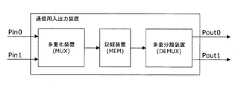
従来、インターネット等のデータ通信で使用されて、例えばイーサネット(登録商標)のフレームデータ等の通信データを入出力するための通信用入出力装置として、例えば、特許文献1のような構成が提案されている。図27は、従来の通信用入出力装置(内蔵メモリ)の構成を示すブロック図である。
この通信用入出力装置は、多重化装置MUX、記録装置MEM、および多重分離装置DEMUXから構成されている。Conventionally, for example, a configuration as disclosed in
This communication input / output device includes a multiplexing device MUX, a recording device MEM, and a demultiplexing device DEMUX.
MUXは、入力ポートごとに設けられたキュー指定情報付加部により、入力されたフレームデータに対して、当該フレームデータの出力先に対応するキュー指定情報を付加した後、多重化部により多重化して出力する。
MEMは、MUXから時分割多重で出力されたフレームデータを書込制御部により受け取り、各フレームデータに付加されているキュー指定情報とキューマップとを参照し、内蔵するデータメモリ内にフレームデータの出力先ごとに論理的に設けたキューのうち、キュー指定情報と対応するキューのアドレスへフレームデータを書き込む。また、MEMは、DEMUXからの読出指示に応じて、読出制御部により対応するキューからフレームデータを読み出して、DEMUXに出力する。The MUX adds the queue designation information corresponding to the output destination of the frame data to the input frame data by the queue designation information addition section provided for each input port, and then multiplexes it by the multiplexing section. Output.
The MEM receives the frame data output from the MUX by time division multiplexing by the write control unit, refers to the queue designation information and the queue map added to each frame data, and stores the frame data in the built-in data memory. Of the queues logically provided for each output destination, the frame data is written to the queue address corresponding to the queue designation information. Further, in response to a read instruction from the DEMUX, the MEM reads frame data from the corresponding queue by the read control unit and outputs the frame data to the DEMUX.
DEMUXは、読出部により、出力ポートごとの優先制御ロジックに基づき、MEM内の優先出力ポートに対応する出力先のキューからフレームデータを読み出して、振分部により対応する出力ポートへ振り分け、出力ポートごとに設けられた速度変換部により当該出力ポートの通信速度に変換して出力する。 The DEMUX reads out the frame data from the output destination queue corresponding to the priority output port in the MEM based on the priority control logic for each output port by the reading unit, and distributes the frame data to the corresponding output port by the distribution unit. The data is converted into the communication speed of the output port by a speed conversion unit provided for each output.
図28は、キューと出力ポートとの対応を示す説明図であり、出力ポート数が3の場合が示されている。図28(a)では、キューと出力ポートとが1対1に対応付けられているが、図28(b)のように、1対多に対応付けることにより、1つのフレームデータを複数の出力ポートが出力する場合に対応可能となる。また、図28(c)のように、出力ポートごとに、読出優先度に応じたキューを対応付けることもできる。 FIG. 28 is an explanatory diagram showing the correspondence between queues and output ports, and shows the case where the number of output ports is three. In FIG. 28A, queues and output ports are associated one-to-one, but as shown in FIG. 28B, one frame data is associated with a plurality of output ports. Can be handled when In addition, as shown in FIG. 28C, a queue corresponding to the read priority can be associated with each output port.
このような通信用入出力装置では、出力系統の増加に応じてMEMで必要とされる記憶容量が増大するため、データメモリとしてDRAMが用いられる。しかしながら、DRAMのアクセスには、各バンクにおけるロウアドレスの活性化に起因して待ち時間が発生するため、場合によっては、DRAMアクセスの実効スループットが極端に低下して、フレームデータの処理速度に追従できなくなり、通信品質が劣化するという問題点があった。 In such a communication input / output device, the storage capacity required by the MEM increases as the output system increases, so a DRAM is used as a data memory. However, since DRAM access has a waiting time due to the activation of the row address in each bank, in some cases, the effective throughput of the DRAM access is extremely reduced to follow the processing speed of frame data. There is a problem that communication quality is deteriorated because communication cannot be performed.
一般に、DRAMでは、任意のバンクの任意のロウアドレスにデータを書き込む場合、当該バンクにおいて当該ロウアドレスを活性化する必要があり、同一バンクの異なるロウアドレスにアクセスする場合には、当該ロウアドレスを用いたアクセスが完了するのを待ってから、新たなロウアドレスを活性化する必要があるため、同一バンクへのアクセスにおいて、ロウアドレスの活性化に起因して比較的大きな待ち時間が発生する。具体的には、同一バンクの異なるロウアドレスへのアクセスが連続した場合である。その他に待ち時間が発生する条件として、読み出し後の同一バンクに書き込みを行う場合、および、書き込み後の同一バンクから読み出しを行う場合がある。 In general, in a DRAM, when writing data to an arbitrary row address of an arbitrary bank, it is necessary to activate the row address in the bank. When accessing a different row address of the same bank, the row address is Since it is necessary to activate a new row address after waiting for the used access to be completed, a relatively large waiting time occurs due to the activation of the row address in accessing the same bank. Specifically, this is a case where accesses to different row addresses in the same bank are continuous. As other conditions for waiting time, there are a case where writing is performed in the same bank after reading and a case where reading is performed from the same bank after writing.
したがって、これら待ち時間がDRAMアクセスに関する実効スループットの低下原因となる。このため、特に、通信用入出力装置においては、短いフレームデータがバースト的に連続して入力される場合があり、このようなケースにおいて、頻繁に同一バンクの異なるロウアドレスへアクセスを行った場合、極端に実効スループットが低下する可能性がある。また、活性化処理が頻繁に発生するため電力消費が増大する。 Therefore, these waiting times cause a decrease in effective throughput related to DRAM access. Therefore, in particular, in communication I / O devices, short frame data may be input continuously in bursts. In such a case, when frequently accessing different row addresses in the same bank The effective throughput may be extremely reduced. In addition, since the activation process occurs frequently, power consumption increases.
本発明はこのような課題を解決するためのものであり、DRAMアクセスに関する実効スループットの低下を抑制でき、活性化処理に起因する電力消費を削減できるメモリアクセス制御技術を提供することを目的としている。 An object of the present invention is to provide a memory access control technique that can suppress a decrease in effective throughput related to DRAM access and reduce power consumption caused by activation processing. .
このような目的を達成するために、本発明にかかる通信用入出力装置は、順次入力される通信データに、当該通信データを出力すべき出力系統と対応するキューを示すキュー指定情報を付加して多重化する多重化装置と、前記多重化装置から転送された前記通信データを、データメモリ内に論理的に形成した複数のキューのうち前記キュー指定情報で指定された書込対象キューへ一時蓄積する記録装置と、前記キューのうち優先制御ロジックに基づき選択した出力系統と対応する読出対象キューから前記通信データを読み出し、当該出力系統と対応する出力ポートの通信速度に変換して出力する多重分離装置とを備える通信用入出力装置であって、前記記録装置は、バンクごとにライトポインタを有するDRAMからなり、前記キューの通信データを記憶する前記データメモリと、前記バンクごとに前記ライトポインタのロウアドレスが活性化状態であるか否かを示す活性化状態フラグを記憶するキュー制御メモリと、前記書込対象キューに前記通信データを書き込む際、前記バンクのうち活性化状態フラグが活性化状態であることを示しているバンクを書込対象バンクとして選択して当該通信データを書き込み、活性化状態フラグが活性化状態であることを示しているバンクが存在しない場合は、活性化状態フラグが非活性化状態であることを示しているバンクを書込対象バンクとして選択して当該バンクのライトポインタのロウアドレスを活性化した後に当該通信データを書き込むDRAMアクセス部とを備えている。 In order to achieve such an object, the communication input / output device according to the present invention adds queue designation information indicating a queue corresponding to an output system to which the communication data is to be output to communication data that is sequentially input. And the communication data transferred from the multiplexing device are temporarily stored in a write target queue designated by the queue designation information among a plurality of queues logically formed in a data memory. Multiplex that reads out the communication data from the queue to be read corresponding to the output system selected from the queue and the output system selected based on the priority control logic from the queue, converts it to the communication speed of the output port corresponding to the output system, and outputs it A communication input / output device comprising a separation device, wherein the recording device comprises a DRAM having a write pointer for each bank, and communication of the queue The data memory for storing data, a queue control memory for storing an activation state flag indicating whether or not the row address of the write pointer is in an activated state for each bank, and the write target queue with the queue When writing communication data, the bank indicating that the activation state flag is in the activated state among the banks is selected as the write target bank, the communication data is written, and the activation state flag is in the activated state. If there is no bank indicating that there is a bank, the bank indicating that the activation state flag is in the inactive state is selected as the bank to be written, and the row address of the write pointer in that bank is activated. And a DRAM access unit for writing the communication data.
また、本発明にかかる上記通信用入出力装置の一構成例は、前記記録装置が、前記データメモリの前記キューに対する書き込み・読み出しを制御する際に用いるキュー制御情報を記憶するキュー制御メモリと、前記キュー制御メモリのキュー制御情報に基づいて、前記多重化装置から転送された前記通信データの前記書込対象キューに対する書き込みを前記DRAMアクセス部に指示する書込制御部と、前記キュー制御メモリのキュー制御情報に基づいて、前記読出対象キューからの通信データの読み出しを前記DRAMアクセス部に指示し、読み出した通信データを前記多重分離装置へ転送する読出制御部とをさらに備え、前記キュー制御メモリは、前記活性化状態フラグを前記バンクごとに記憶するとともに、仮想データメモリ上で用いられる仮想格納アドレスごとに、当該仮想格納アドレスに書き込まれた通信データに後続する通信データの仮想格納アドレスを示す後続アドレスを記憶し、前記キューごとに、当該キューの通信データが書き込まれている前記仮想格納アドレスの先頭および最終を示すキュー先頭アドレスおよびキュー最終アドレスを記憶し、前記キューのそれぞれに共通して、前記ライトポインタとバンクごとに1対1に対応して次に通信データを書き込むべき仮想格納アドレスを示すバンクごとの次書込アドレスを記憶し、前記書込制御部は、前記書込対象キューに前記通信データを書き込む際、前記書込対象バンクとして選択したバンクの前記次書込アドレスからなる書込対象仮想アドレスに対する当該通信データの書き込みをDRAMアクセス部に指示し、当該書込対象キューのキュー最終アドレス、書込前のキュー最終アドレスに関する後続アドレス、および書込対象バンクとして選択したバンクの次書込アドレスをそれぞれ更新し、前記書込対象バンクの書込対象仮想アドレスに対応する現在のライトポインタのロウアドレスと更新後の次書込アドレスに対応する更新後のライトポインタのロウアドレスとが同じ場合は、前記書込対象バンクの活性化状態フラグを活性化状態であることを示す値とし、前記ロウアドレスが互いに異なる場合は、前記活性化状態フラグを非活性化状態とし、前記読出制御部は、前記読出対象キューから前記通信データを読み出す際、当該読出対象キューのキュー先頭アドレスからなる読出対象仮想アドレスに対する当該通信データの読み出しをDRAMアクセス部に指示し、当該読出対象キューのキュー先頭アドレス、読出対象バンクの次書込アドレス、および新たな読出対象バンクの次書込アドレスに関する後続アドレスをそれぞれ更新し、前記読出対象バンクの読出対象仮想アドレスに対応するリードポインタのロウアドレスと更新後の次書込アドレスに対応する更新後のライトポインタのロウアドレスとが同じ場合は、前記読出対象バンクの活性化状態フラグを活性化状態であることを示す値とし、前記ロウアドレスが互いに異なる場合は、前記活性化状態フラグを非活性化状態とするようにしたものである。 In addition, one configuration example of the communication input / output device according to the present invention includes: a queue control memory that stores queue control information used when the recording device controls writing / reading to / from the queue of the data memory; A write control unit that instructs the DRAM access unit to write the communication data transferred from the multiplexing device to the write target queue based on queue control information in the queue control memory; A read control unit for instructing the DRAM access unit to read communication data from the read target queue based on queue control information, and transferring the read communication data to the demultiplexing device; Stores the activation state flag for each bank and uses it on the virtual data memory For each virtual storage address, a subsequent address indicating a virtual storage address of communication data subsequent to the communication data written to the virtual storage address is stored, and the communication data of the queue is written for each queue A queue head address and a queue last address indicating the head and end of the virtual storage address are stored, and in common with each of the queues, communication data should be written next in a one-to-one correspondence with the write pointer for each bank. A next write address for each bank indicating a virtual storage address is stored, and the write control unit writes the communication data to the write target queue, and the next write of the bank selected as the write target bank Directs the DRAM access unit to write the communication data to the write target virtual address. Update the queue final address of the write target queue, the subsequent address related to the queue final address before writing, and the next write address of the bank selected as the write target bank, respectively. If the current write pointer row address corresponding to the target virtual address is the same as the updated write pointer row address corresponding to the updated next write address, the activation status flag of the write target bank is activated. When the row address is different from each other, the activation state flag is deactivated and the read control unit reads the communication data from the read target queue. Reads the communication data to the read target virtual address consisting of the queue head address of the read target queue. And instructing the access unit to update the queue start address of the read target queue, the next write address of the read target bank, and the subsequent address related to the next write address of the new read target bank, respectively. If the row address of the read pointer corresponding to the virtual address is the same as the row address of the updated write pointer corresponding to the updated next write address, the activation state flag of the read target bank is in the activated state. When the row addresses are different from each other, the activation state flag is inactivated.
また、本発明にかかる上記通信用入出力装置の一構成例は、前記記録装置が、前記キューごとに、当該キューが使用している前記仮想データメモリ上での仮想格納アドレスの数を示す使用アドレス数を記憶するキュー使用アドレス数メモリと、前記書込対象キューに前記通信データを書き込む際、当該通信データのデータ長に基づき、書き込みに必要となる仮想格納アドレスの数を示す必要アドレス数を算出し、前記キュー使用アドレス数メモリから取得した当該書込対象キューまたは前記キューの使用アドレス数に基づき、当該書き込みに使用可能な仮想格納アドレスの数を示す残りアドレス数を算出し、当該必要アドレス数と当該残りアドレス数とを比較することにより当該通信データの書込可否を判定し、書込可の判定に応じて当該通信データの書き込みを指示するアクセス調停部とをさらに備えるようにしたものである。 Also, in one configuration example of the communication input / output device according to the present invention, the recording device uses, for each queue, the number of virtual storage addresses on the virtual data memory used by the queue. Queue use address number memory for storing the number of addresses, and when writing the communication data to the write target queue, based on the data length of the communication data, the required address number indicating the number of virtual storage addresses required for writing Calculate the remaining number of addresses indicating the number of virtual storage addresses that can be used for the writing based on the number of used addresses of the write target queue or the queue acquired from the queue used address number memory and calculate the necessary address Is compared with the number of remaining addresses to determine whether or not the communication data can be written. Is obtained so as to further include an access arbitration unit for instructing the writing of data.
本発明によれば、多重化装置から転送された通信データを、データメモリ内に論理的に形成した複数のキューのうちキュー指定情報で指定された書込対象キューへ一時蓄積する記録装置において、データメモリをDRAMで構成した場合でも、ロウアドレスの活性化回数を低減することができる。このため、DRAMアクセスに関する実効スループットの低下を抑制でき、活性化処理に起因する電力消費を削減することが可能となる。
また、キュー制御情報を記憶するキュー制御メモリに、通信データ書き込み時に選択したバンクの情報を記憶でき、その情報を該当の通信データの読み出し時に使用できる。According to the present invention, in a recording device for temporarily storing communication data transferred from a multiplexing device in a write target queue designated by queue designation information among a plurality of queues logically formed in a data memory, Even when the data memory is composed of a DRAM, the number of activations of the row address can be reduced. For this reason, it is possible to suppress a decrease in effective throughput related to DRAM access, and it is possible to reduce power consumption caused by activation processing.
Further, the queue control memory for storing the queue control information can store the information of the bank selected at the time of writing the communication data, and can use the information at the time of reading the corresponding communication data.
次に、本発明の実施の形態について図面を参照して説明する。
[第1の実施の形態]
まず、図1を参照して、本発明の第1の実施の形態にかかる通信用入出力装置1について説明する。図1は、第1の実施の形態にかかる通信用入出力装置の構成を示すブロック図である。Next, embodiments of the present invention will be described with reference to the drawings.
[First Embodiment]
First, a communication input /
この通信用入出力装置1は、インターネット通信等で使用されて、例えばイーサネット(登録商標)のフレームデータ等の通信データを入出力するための通信用入出力装置であり、1つまたは複数の入力ポートから入力された通信データを、その通信データを出力すべき出力系統ごとに分離し、当該出力系統と対応する出力ポートの通信速度に変換して出力する機能を有している。 The communication input /
図1に示すように、通信用入出力装置1は、多重化装置(MUX)10、メモリアクセス制御機能内蔵型の多重分離装置(DEMUX)20、およびアクセス制御機能内蔵型の記録装置(MEM)30から構成されている。以下では、通信用入出力装置1で入出力する通信データがフレームデータである場合を例として説明するが、これに限定されるものではなく、パケットやATMセルなど各種の通信データを、フレームデータと同様にして入出力することも可能である。 As shown in FIG. 1, the communication input /
多重化装置10は、外部から順次入力されるフレームデータに、当該フレームデータを出力すべき出力系統と対応するキュー指定情報を付加して多重化する機能を有している。
記録装置30は、多重化装置10から転送されたフレームデータを、データメモリ内に論理的に形成した複数のキューのうち、当該フレームデータに付加されているキュー指定情報で指定された書込対象キューへ一時蓄積する機能を有している。
多重分離装置20は、記録装置30内のキューのうち優先制御に基づき選択した出力系統と対応する読出対象キューから、当該読出対象キューに一時蓄積されているフレームデータを読み出し、当該出力系統と対応する出力ポートの通信速度に変換して出力する機能を有している。The multiplexing
The
The
本実施の形態は、記録装置30において、データメモリ31をバンクごとにライトポインタを有するDRAMから構成して、バンクごとにライトポインタのロウアドレスが活性化状態であるか否かを示す活性化状態フラグを記憶するキュー制御メモリ33を備え、DRAMアクセス部32が、書込対象キューにフレームデータを書き込む際、バンクのうち活性化状態フラグが活性化状態であることを示しているバンクを書込対象バンクとして選択して当該フレームデータを書き込み、活性化状態フラグが活性化状態であることを示しているバンクが存在しない場合は、活性化状態フラグが非活性化状態であることを示しているバンクを書込対象バンクとして選択して当該バンクのライトポインタのロウアドレスを活性化した後に当該フレームデータを書き込むようにしたものである。 In the present embodiment, in the
本実施の形態では、図1に示すように、入力ポートPinとして2つの入力ポートPin0,Pin1が設けられ、出力ポートPoutとして2つの出力ポートPout0,Pout1が設けられている場合を例として説明するが、入力ポートPinおよび出力ポートPoutの数については、これに限定されるものではない。入力ポートPinおよび出力ポートPoutのいずれか一方または両方を3つ以上設けることも可能であり、入力ポート数と出力ポート数が異なっていてもよい。なお、入力ポート数は、1つであってもよい。 In this embodiment, as shown in FIG. 1, a case where two input ports Pin0 and Pin1 are provided as the input port Pin and two output ports Pout0 and Pout1 are provided as the output port Pout will be described as an example. However, the number of input ports Pin and output ports Pout is not limited to this. Three or more of either or both of the input port Pin and the output port Pout can be provided, and the number of input ports and the number of output ports may be different. Note that the number of input ports may be one.
[多重化装置]
次に、図1を参照して、本実施の形態にかかる通信用入出力装置1で用いられる多重化装置10について詳細に説明する。
図1に示すように、多重化装置10には、主な回路部として、キュー指定情報付加部11と多重化部12が設けられている。[Multiplexer]
Next, with reference to FIG. 1, the multiplexing
As shown in FIG. 1, the multiplexing
キュー指定情報付加部11は、入力ポートPin0,Pin1ごとに設けられて、対応する入力ポートPinから入力されるフレームデータに対して、当該フレームデータの出力先に対応するキュー指定情報と、当該フレームデータのフレーム長情報(Byte)とを付加して多重化部12へ出力する機能を有している。この際、フレーム長情報については、例えば、多重化部12にフレームデータを出力する際、当該フレームデータの先頭から最終までのByte数をフレーム長として計数したものを付加すればよい。 The queue designation
多重化部12は、各キュー指定情報付加部11に共通して1つ設けられて、各キュー指定情報付加部11から出力されたフレームデータを時分割で多重化して、記録装置30へ出力する機能を有している。
多重化装置10において、フレームデータの出力先に対応するキューの指定については、IEEE802.1D等のブリッジ機能により実現すればよく、具体的には、MACアドレス学習による出力ポート検索、VLAN−IDによる出力ポート指定等が可能である(特許文献1など参照)。Multiplexing
In the
[多重分離装置]
次に、図1を参照して、本実施の形態にかかる通信用入出力装置1で用いられる多重分離装置20について詳細説明する。
図1に示すように、多重分離装置20には、主な回路部として、読出部21、振分部22、および速度変換部23,24が設けられている。[Demultiplexer]
Next, the
As shown in FIG. 1, the
読出部21は、記録装置30から取得した各キューの蓄積状況や速度変換部23,24から出力された読出停止指示信号を参照し、出力ポートPout0,Pout1ごとの優先制御ロジックに基づいてフレームデータを優先して出力すべき出力系統を選択する機能と、当該出力系統と対応する読出対象キューからのフレームデータの読み出しを要求する読み出し要求を出力する機能と、これに応じて記録装置30から転送されたフレームデータを、振分部22へ出力する機能を有している。
優先制御ロジックについては、例えば各キューの容量が同じ場合であれば、読み出し可能なキューの中でキューに蓄積されている通信データの量が最も多いキューから読み出しを行う等、一般的な優先制御ロジックを用いればよい(特許文献1など参照)。The
For priority control logic, for example, if the capacity of each queue is the same, general priority control such as reading from the queue with the largest amount of communication data stored in the queue among readable queues. Logic may be used (see Patent Document 1).
また、読出部21は、記録装置30に読み出し要求を出力する際、読み出し対象となるキューを指定するキュー指定情報に加えて、読み出しデータのデータ量を示す読出データ量情報を記録装置30に指示する。
読出データ量情報については、例えば読み出しを行うキューのデータ蓄積量が予め設定した閾値以下の場合は、データ蓄積量に等しい値を読出データ量情報として出力し、閾値を超えていた場合は、閾値の値を読出データ量情報として出力すればよい。In addition, when the
For the read data amount information, for example, when the data accumulation amount of the queue to be read is equal to or less than a preset threshold value, a value equal to the data accumulation amount is output as the read data amount information. May be output as read data amount information.
振分部22は、読出部21から出力されたフレームデータを、当該フレームデータに付加されているキュー指定情報に基づいて、対応する出力ポートの速度変換部23,24へ振り分ける機能を有している。
速度変換部23,24は、出力ポートごとに設けられて、振分部22から振り分けられたフレームデータを当該出力ポートの通信速度に変換して出力する機能と、フレームデータの出力状況に応じて読出停止指示信号を読出部21に出力する機能とを有している。
なお、フレームデータに付加されているキュー指定情報は、振分部22もしくは速度変換部23,24で削除される。The
The
The queue designation information added to the frame data is deleted by the
[記録装置]
次に、図1を参照して、本実施の形態にかかる通信用入出力装置1で用いられる記録装置30について詳細説明する。[Recording device]
Next, the
図1に示すように、記録装置30には、主な回路部として、データメモリ31、DRAMアクセス部32、キュー制御メモリ33、書込制御部34、読出制御部35、キュー使用アドレス数メモリ36、およびアクセス調停部37が設けられている。 As shown in FIG. 1, the
データメモリ31は、バンク(Bank)ごとに複数のロウアドレス(Row Address)を有する一般的なDRAM(DRAMチップ)からなり、バンクごとのライトポインタを用いてフレームデータを記憶する機能を有している。具体的には、データメモリ31を1つ、もしくは、複数のDRAMチップで構成して、バンクごとのライトポインタに対応させればよく、出力系統ごとにそれぞれ1つのキューを持たせる構成の他、1つの出力系統に複数のキューを持たせることも可能である。本実施の形態では、1つのDRAMチップを複数のキューで共用することになる。 The
データメモリ31には、固有の格納アドレスを持つ複数の格納領域が設けられている。各キューはデータメモリ31の格納アドレスと同等な仮想格納アドレスを持つ仮想データメモリの仮想格納領域を、仮想格納アドレスの連続・不連続あるいは昇順・降順に関わらず任意に連結することにより構成されている。なお、仮想格納アドレスは、DRAMへのアクセスに用いる実際のロウアドレス、コラムアドレス(Column Address)、およびバンク番号とは独立した、フレームデータの管理に用いられるものであり、仮想的なメモリ空間におけるアドレス情報である。 The
仮想格納アドレスと実際のロウアドレスおよびコラムアドレスの組とは、バンクごとに1対1に対応する。同様に、次書込アドレスと、ライトポインタ(ロウアドレスとコラムアドレスを含む)も1対1に対応する。
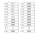
図2は、仮想データメモリの記憶例である。ここでは、それぞれ固有の仮想格納アドレスADM(0〜N:Nは2以上の整数)を持つ仮想格納領域ごとに、書込制御部34から書き込まれたデータを記憶している場合のイメージを示している。The virtual storage address and the set of the actual row address and column address correspond to each bank on a one-to-one basis. Similarly, the next write address and the write pointer (including the row address and the column address) have a one-to-one correspondence.
FIG. 2 is a storage example of the virtual data memory. Here, an image in a case where data written from the
この際、1フレームが1仮想アドレス分のデータサイズより長い場合、1フレームは、1仮想アドレス分のデータサイズに合わせて複数のデータDに分割され、それぞれ異なる複数の仮想格納アドレスに書き込まれる。例えば、図2の場合、バンク0の仮想格納アドレス0,1,4には、キューP1のデータP1−1,P1−2,P1−3が格納されており、バンク0の仮想格納アドレス2,3,5には、キューP2のデータP2−1,P2−2,P2−3が格納されている。これらデータの前後関係やフレームとの対応関係については、後述するアドレスキュー管理メモリで管理される。なお、1フレームが仮想格納領域のデータサイズより短い場合、フレームデータは1つの仮想格納領域に格納される。 At this time, if one frame is longer than the data size for one virtual address, one frame is divided into a plurality of data D in accordance with the data size for one virtual address, and written to a plurality of different virtual storage addresses. For example, in the case of FIG. 2, the virtual storage addresses 0, 1, and 4 of the
DRAMアクセス部32は、書込制御部34からのDRAM書込指示に応じて、データメモリ31内の対応するアドレスにフレームデータを書き込む機能と、読出制御部35からのDRAM読出指示に応じて、データメモリ31内の対応するアドレスからフレームデータを読み出す機能とを有している。 The
DRAMアクセス部32は、フレームデータを書き込む際、指示されたバンクの書込対象ロウアドレスが活性化状態にある場合に、指定された仮想格納アドレス(ロウアドレスおよびコラムアドレス)にフレームデータを書き込む機能と、当該書込対象ロウアドレスが活性化状態にない場合は、当該書込対象ロウアドレスを活性化した後にフレームデータを書き込む機能とを有している。 The
また、DRAMアクセス部32は、フレームデータを読み出す際、指示された読出対象バンクにおいて読出対象ロウアドレスが活性化状態にある場合は、当該読出対象バンクの読出対象ロウアドレスからフレームデータを読み出し、当該読出対象バンクで読出対象ロウアドレスが活性化状態にない場合は、当該読出対象バンクの読出対象ロウアドレスを活性化した後にフレームデータを読み出す機能とを有している。 When reading the frame data, the
キュー制御メモリ33は、例えばSRAMチップなどの半導体メモリからなり、データメモリ31上に形成されている各キューに対するフレームデータの書き込み・読み出しを制御する際に用いる各種のキュー制御情報を記憶する機能を有している。 The
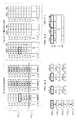
図3は、キュー制御メモリの構成を示すブロック図である。キュー制御メモリ33は、レジスタやメモリからなる複数の記憶部を含んでおり、主な記憶部として、空きアドレスレジスタ(VAR,UAR)33A、アドレスキュー管理メモリ(QM)33B、キュー先頭アドレスレジスタ(SAR)33C、キュー最終アドレスレジスタ(LAR)33D、アクセス履歴レジスタ(AAR)33E、作業用アドレスレジスタ(TMPV,TMPL,TMPS)33F、および、活性化状態フラグレジスタ(AFR)33Gを有している。なお、以下では理解を容易とするため、レジスタ名を変数名として用いて説明する場合がある。 FIG. 3 is a block diagram showing the configuration of the queue control memory. The
空きアドレスレジスタ(VAR,UAR)33Aは、各キューに共通して、バンク毎に次書込アドレスVARと未書込アドレスUARとを記憶する機能を有している。このうち、VAR(Valid Address Register)は、多重化装置10から次に受け取ったフレームデータを書き込む際、当該フレームデータを次に書き込むべき仮想格納アドレスを示すバンク毎のアドレス情報である。また、UAR(Unused Address Register)は、初期化後にまだ一度もデータが書き込まれていない同一バンク内の未使用の仮想格納アドレスのうちの先頭(若番)を示す格納アドレスである。 The empty address register (VAR, UAR) 33A has a function of storing the next write address VAR and the unwritten address UAR for each bank in common with each queue. Among them, VAR (Valid Address Register) is address information for each bank indicating a virtual storage address where the frame data to be written next when the frame data received from the multiplexing
本実施の形態では、フレームデータ書き込み時、各バンク内では、仮想格納アドレスの若番から順に使用することを基本としており、フレームデータの読み出しにより空き状態となった仮想格納アドレスについては、未使用の仮想格納アドレスより優先して再使用するものとする。なお、再使用する仮想格納アドレスの順序については、例えば直近に空き状態となった仮想格納アドレスから順に再使用するなど、任意の順序でよく、若番の順に限定されない。 In this embodiment, when writing frame data, it is basically used in order from the youngest virtual storage address in each bank, and the virtual storage address that has become free by reading frame data is unused. It shall be reused in preference to the virtual storage address. The order of the virtual storage addresses to be reused may be any order, for example, the virtual storage addresses that have recently become empty, and may be reused in order, and is not limited to the lowest number.
アドレスキュー管理メモリ(QM)33Bは、仮想格納アドレスADMごとに、後続仮想アドレスADD(ADDress)とポインタPN(Pointer of QM)とを記憶する機能を有している。
図4は、アドレスキュー管理メモリの記憶例である。このうち、ADDは、当該仮想格納アドレスに書き込まれた通信データに後続する通信データが格納されている仮想格納アドレス(バンク情報を含む)である。また、PNは、当該仮想格納アドレスに格納されているデータにフレームデータの最終データを含むか否かを示す情報(フレーム終端フラグ:EoF)である。The address queue management memory (QM) 33B has a function of storing a subsequent virtual address ADD (ADDress) and a pointer PN (Pointer of QM) for each virtual storage address ADM.
FIG. 4 is a storage example of the address queue management memory. Among these, ADD is a virtual storage address (including bank information) in which communication data following the communication data written to the virtual storage address is stored. PN is information (frame end flag: EoF) indicating whether or not the data stored at the virtual storage address includes the final data of the frame data.
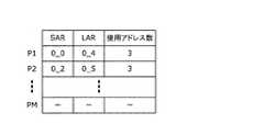
キュー先頭アドレスレジスタ(SAR)33Cは、キューごとに、キュー先頭アドレスSAR(Start Address register of PM)を記憶する機能を有している。
キュー最終アドレスレジスタ(LAR)33Dは、キューごとに、キュー最終アドレスLAR(Last Address register of PM)を記憶する機能を有している。The queue head address register (SAR) 33C has a function of storing a queue head address SAR (Start Address register of PM) for each queue.
The queue last address register (LAR) 33D has a function of storing a queue last address LAR (Last Address register of PM) for each queue.
図5は、キュー先頭アドレスレジスタおよびキュー最終アドレスレジスタの記憶例である。ここでは、キューを識別するためのキューID(キュー番号)ごとに、SARとLARを記憶している。このうち、SARは、当該キューのフレームデータが書き込まれている仮想格納アドレスの先頭を示すアドレス情報(バンク情報を含む)である。また、LARは、当該キューのフレームデータが書き込まれている仮想格納アドレスの最終を示すアドレス情報(バンク情報を含む)である。 FIG. 5 shows a storage example of the queue head address register and the queue last address register. Here, SAR and LAR are stored for each queue ID (queue number) for identifying the queue. Among these, SAR is address information (including bank information) indicating the head of the virtual storage address in which the frame data of the queue is written. LAR is address information (including bank information) indicating the end of the virtual storage address in which the frame data of the queue is written.
アクセス履歴レジスタ(AAR)33Eは、最後に書き込み指示、もしくは、読み出し指示を行った仮想格納アドレス(バンク情報を含む)をAAR_1として記録し、AAR_nはAAR_1の更新時にAAR_(n−1)の値に更新する(nは2以上の整数)。すなわち、直近n回分の書き込み指示、もしくは、読み出し指示の履歴を表示する。 The access history register (AAR) 33E records the virtual storage address (including bank information) at which the last write instruction or read instruction is recorded as AAR_1, and AAR_n is the value of AAR_ (n-1) when AAR_1 is updated. (N is an integer of 2 or more). That is, the history of the latest n write instructions or read instructions is displayed.
作業用アドレスレジスタ(TMPV,TMPL,TMPS)33Fは、各キューに共通して、作業用次書込アドレスTMPV(Temporary register for VAR)と、作業用キュー最終アドレスTMPL(Temporary register for LAR)と、作業用キュー先頭アドレスTMPS(Temporary register for SAR)とを記憶する機能を有している。 The work address register (TMPV, TMPL, TMPS) 33F is common to each queue, the work next write address TMPV (Temporary register for VAR), the work queue final address TMPL (Temporary register for LAR), It has a function of storing a work queue head address TMPS (Temporary register for SAR).
このうち、TMPVは、書き込み・読み出しを行うバンクの直前(更新前)の次書込アドレスVARを示すアドレス情報(バンク情報を含む)である。また、TMPLは、書き込みを行うキューの直前(更新前)のキュー最終アドレスLARである。TMPSは、読み出しを行うキューの直前(更新前)のキュー先頭アドレスSARを示すアドレス情報(バンク情報を含む)である。これらは、それぞれのデータの書き込み・読み出し作業の処理手順の関係から一時的にアドレス情報を保持するために使用されるものであるが、次の書き込み・読み出し作業に用いることもある。 Among these, TMPV is address information (including bank information) indicating the next write address VAR immediately before (before update) the bank in which writing / reading is performed. TMPL is the queue final address LAR immediately before (before update) the queue for writing. TMPS is address information (including bank information) indicating the queue head address SAR immediately before (before update) the queue to be read. These are used to temporarily hold address information because of the processing procedure of each data write / read operation, but may also be used for the next write / read operation.
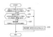
活性化状態フラグレジスタ(AFR)33Gは、各キューに共通して、バンク毎に活性化状態フラグAFRを記憶する機能を有している。AFR(Active Flag register)は、VARのロウアドレスが活性化状態であることを示すバンク毎のフラグである。書き込み・読み出しの対象となるバンクにおいて、書き込み・読み出し対象のロウアドレスと更新後のVARに対応する更新後のライトポインタのロウアドレスが同じ場合は、更新後のVARのロウアドレスが既に活性化状態なので、更新後の活性化状態フラグAFRを活性化状態であることを示す値とする。ロウアドレスが異なる場合は、更新後のVARのロウアドレスが非活性化状態なので、更新後の活性化状態フラグAFRを非活性化状態であることを示す値とする。 The activation state flag register (AFR) 33G has a function of storing an activation state flag AFR for each bank in common with each queue. An AFR (Active Flag Register) is a flag for each bank indicating that the VAR row address is in an activated state. If the row address of the write / read target and the row address of the updated write pointer corresponding to the updated VAR are the same in the bank to be written / read, the row address of the updated VAR is already activated. Therefore, the updated activation state flag AFR is set to a value indicating the activated state. If the row address is different, the updated VAR row address is in an inactive state, and therefore the updated activation state flag AFR is set to a value indicating that it is in an inactive state.
書込制御部34は、アクセス調停部37からの書き込み指示に応じて、アクセス履歴レジスタ(AAR)とバンク毎のVAR、UAR、およびAFRに基づいて、以下の最適バンク選択処理を実行することにより最適なバンクのVARを選択し、仮想格納アドレス(TMPV)を指定した、フレームデータの書き込みを指示するDRAM書込指示を、DRAMアクセス部32へ出力する機能を有している。 In response to a write instruction from the
図6は、最適バンク選択処理を示すフローチャートである。バンク(VAR)の選択は例えば、図6に示す手順で行う。
書込制御部34は、AARを用いてアクセス履歴が残っている各バンクでどのロウアドレスが活性化されているのかを管理している。また、バンク毎のAFRを用いて各バンクのVARのロウアドレスが活性化状態であるか否かを管理している。
書込制御部34は、これらAARおよびAFRを参照して、各バンクのVARのロウアドレスの内、活性化されているものを選択する。ただし、該当バンクのUARとVARの両方がバンク毎のメモリ容量の上限値に到達している場合には、該当バンクが満杯なので書き込み不可能なため、そのバンクは選択しない。FIG. 6 is a flowchart showing the optimum bank selection process. The selection of the bank (VAR) is performed, for example, according to the procedure shown in FIG.
The
The
なお、活性処理から書き込み・読み出しまでの所要時間が、書き込み・読み出し指示の最小入力間隔のn_min倍である場合、少なくとも直近n_min回分のAAR値を保持する必要がある。したがって、AARの履歴数nはn_min以上の数となる。後述する図15〜図21の説明図では、n=n_min=5の場合を例として説明している。アクセス履歴AAR_1〜AAR_(n_min)のいずれにも記録されていないバンクは、先行処理が既に完了しているので次の活性化処理をすぐに開始でき、直前の書き込み・読み出しから最少間隔で(スループット低下なしで)書き込みを行うことができる。一方、AAR_1〜AAR_(n_min)のいずれかに記録されているバンクは、進行中の先行処理が終わるまでは次の活性化処理を開始できないので、先行処理が完了するまで待つためスループットが低下する。 When the time required from the activation process to writing / reading is n_min times the minimum input interval of writing / reading instructions, it is necessary to hold at least the latest n_min AAR values. Accordingly, the history number n of AAR is a number equal to or greater than n_min. In the explanatory diagrams of FIGS. 15 to 21 described later, the case where n = n_min = 5 is described as an example. For banks that are not recorded in any of the access histories AAR_1 to AAR_ (n_min), the previous activation process has already been completed, so the next activation process can be started immediately, with a minimum interval from the previous write / read (throughput). Can be written (without degradation). On the other hand, the bank recorded in any one of AAR_1 to AAR_ (n_min) cannot start the next activation process until the preceding process in progress is completed, so that the throughput decreases because the process waits until the preceding process is completed. .
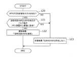
例えば、図6に示すように、まず、書込制御部34は、後述する図7の同一ロウアドレスVAR探索処理を実行することにより、各バンクのうちから、アクセス履歴AAR_1〜AAR_nに記録されている同一バンクの最新アクセス履歴と同じロウアドレスであって、かつ、選択可能なVARを探索する(ステップ100)。
ここで、探索条件に該当するバンクのVARであって、かつ、選択可能なVARが存在する場合(ステップ101:YES)、そのVARのロウアドレスが活性化されているので、そのVARを選択し(ステップ107)、一連の最適バンク選択処理を終了する。同一ロウアドレスVAR探索処理で書き込み先が決定する場合、書き込み先ロウアドレスが既に活性化されているので、活性化処理が不要、且つ、スループット低下が起きない。また、アクセス履歴が残っている範囲内で、ロウアドレスが直前にアクセスされているVARを探索でき、同一バンクの同一ロウアドレスへの連続書き込みを優先的に選択できる。For example, as shown in FIG. 6, first, the
Here, when the VAR of the bank satisfies the search condition and there is a selectable VAR (step 101: YES), the row address of the VAR is activated, so the VAR is selected. (Step 107), a series of optimum bank selection processing ends. When the write destination is determined by the same row address VAR search process, the write destination row address has already been activated, so that the activation process is unnecessary and the throughput does not decrease. Further, it is possible to search for a VAR whose row address has been accessed immediately before the access history remains, and to preferentially select continuous writing to the same row address in the same bank.
一方、AAR_1〜AAR_nに記録されている同一バンクの最新アクセス履歴と同じロウアドレスであってかつ選択可能なVARが存在しない場合(ステップ101:NO)、書込制御部34は、後述する図8の活性状態VAR探索処理を実行することにより、各バンクのうちから、AFRが活性化状態であることを示しているバンクのVARを探索する(ステップ102)。
ここで、探索条件に該当するバンクのVARであって、かつ、選択可能なVARが存在する場合(ステップ103:YES)、そのVARのロウアドレスが活性化されているので、そのVARを選択し(ステップ107)、一連の最適バンク選択処理を終了する。活性状態VAR探索処理で書き込み先が決定する場合、書き込み先ロウアドレスが既に活性化されているので、活性化処理が不要、且つ、スループット低下が起きない。また、アクセス履歴が残っていなくても、ロウアドレスが活性化されているVARが存在すれば、確実に探索できる。On the other hand, when there is no selectable VAR that has the same row address as the latest access history of the same bank recorded in AAR_1 to AAR_n (step 101: NO), the
Here, if the VAR of the bank satisfies the search condition and there is a selectable VAR (step 103: YES), the row address of the VAR is activated, so the VAR is selected. (Step 107), a series of optimum bank selection processing ends. When the write destination is determined by the active state VAR search process, the write destination row address has already been activated, so that the activation process is unnecessary and the throughput does not decrease. Even if no access history remains, if there is a VAR whose row address is activated, the search can be reliably performed.
一方、AFRが活性化状態を示すバンクであって、かつ、選択可能なVARが存在しない場合(ステップ103:NO)、書込制御部34は、後述する図9の記録なしバンクVAR探索処理を実行することにより、各バンクのうちから、AARのアクセス履歴AAR_1〜AAR_(n_min)のいずれにも記録されていない記録なしのバンクのVARを探索する(ステップ104)。
ここで、探索条件に該当するバンクのVARであって、かつ、選択可能なVARが存在する場合(ステップ105:YES)、そのVARを選択し(ステップ107)、一連の最適バンク選択処理を終了する。記録なしバンクVAR探索処理で書き込み先が決定する場合、すぐに活性化処理を開始できるのでスループット低下は起きないが、活性化処理は必要である。On the other hand, when the AFR is in the activated state and there is no selectable VAR (step 103: NO), the
Here, when the VAR of the bank satisfies the search condition and there is a selectable VAR (step 105: YES), the VAR is selected (step 107), and a series of optimum bank selection processing is completed. To do. When the write destination is determined by the bank VAR search process without recording, the activation process can be started immediately, so that the throughput does not decrease, but the activation process is necessary.
一方、記録なしのバンクであって、かつ、選択可能なVARが存在しない場合(ステップ105:NO)、書込制御部34は、後述する図10の先行処理最速完了バンクVAR探索処理を実行することにより、各バンクのうちから、AARのアクセス履歴AAR_1〜AAR_nに記録されている同一バンクの最新アクセス履歴が全バンク中で最古であるバンクのVARを探索し(ステップ106)、そのVARを選択し(ステップ107)、一連の最適バンク選択処理を終了する。記録なしバンクVAR探索処理までで書き込み先が決定しない場合、活性化処理とスループット低下は避けられない。先行処理最速完了バンクVAR探索処理では、最も早く活性化処理を開始できるVARを探索することで、なるべくスループット低下を軽減する。
なお、図6において、ステップ100とステップ102はどちらもロウアドレスが活性化されているVARを探索する処理なので、活性化処理に起因する電力消費を削減できるという点では同等の効果がある。よって、ステップ100−101は、省略してもよい。On the other hand, if the bank is not recorded and there is no selectable VAR (step 105: NO), the
In FIG. 6, since both
次に、図7を参照して、図6のステップ100で実行される同一ロウアドレスVAR探索処理について説明する。図7は、同一ロウアドレスVAR探索処理を示すフローチャートである。
まず、書込制御部34は、AAR選択用パラメータiに「1」を設定し、処理対象AAR_iとしてAAR_1を選択し(ステップ110)、各バンクのVARのうち、バンク番号とロウアドレスの両方がAAR_iと一致するVARを探索する(ステップ111)。ここでは、パラメータiが小さいほど、アクセス履歴AAR_iが新しいものとする。Next, the same row address VAR search process executed in
First, the
ステップ111において、該当するVARが存在する場合(ステップ111:YES)、書込制御部34は、同一ロウアドレスVARとUARの両方がバンク毎のメモリ容量の上限値に該当しているか確認する(ステップ113)。 In
ステップ113において、上限値に該当していない場合(ステップ113:NO)、書込制御部34は、探索結果として、ステップ111で探索した同一ロウアドレスVARを選択し(ステップ117)、一連の同一ロウアドレスVAR探索処理を終了する。 If the upper limit value is not met in step 113 (step 113: NO), the
一方、ステップ111において、該当するVARが存在しない場合(ステップ111:NO)、およびステップ113において、上限値に該当している場合(ステップ113:YES)のそれぞれの場合、書込制御部34は、iとAARの履歴数nとを比較して、すべてのAAR_iに関する探索が完了した確認し(ステップ114)、未探索のAAR_iがあれば(ステップ114:NO)、iをインクリメント(i=i+1)した後(ステップ115)、AAR_iのバンク番号が、それまでに選択したAAR_1〜AAR_(i−1)のいずれかと一致するか確認する(ステップ112)。 On the other hand, in
ステップ112において、一致するバンク番号が存在しない場合(ステップ112:NO)、書込制御部34は、ステップ111へ戻る。
また、ステップ112において、一致するバンク番号が存在する場合(ステップ112:YES)、書込制御部34は、ステップ114へ移行し、未探索のAAR_iがあれば(ステップ114:NO)、iをインクリメント(i=i+1)した後(ステップ115)、ステップ112へ戻る。If there is no matching bank number in step 112 (step 112: NO), the
In
ステップ114において、すべてのAAR_iに関する探索が完了した場合(ステップ114:YES)、書込制御部34は、探索結果として目的のVARが存在しない旨を選択し(ステップ116)、一連の同一ロウアドレスVAR探索処理を終了する。 If the search for all AAR_i is completed in step 114 (step 114: YES), the
次に、図8を参照して、図6のステップ102で実行される活性状態VAR探索処理について説明する。図8は、活性状態VAR探索処理を示すフローチャートである。
まず、書込制御部34は、各バンクのAFRを参照して活性状態を示すバンクを探索し(ステップ120)、活性状態であるバンクが存在する場合(ステップ120:YES)、活性状態VARとUARの両方がバンク毎のメモリ容量の上限値に該当しているか確認する(ステップ121)。Next, the active state VAR search process executed in
First, the
ステップ121において、上限値に該当していない場合(ステップ121:NO)、書込制御部34は、探索結果として、ステップ120で探索した活性状態VARを選択し(ステップ122)、一連の活性状態VAR探索処理を終了する。
一方、ステップ120において、活性状態であるバンクが存在しない場合(ステップ120:NO)、および、ステップ121において、上限値に該当している場合(ステップ121:YES)のそれぞれの場合、書込制御部34は、探索結果として、目的のVARが存在しない旨を選択し(ステップ123)、一連の活性状態VAR探索処理を終了する。If the upper limit is not met in step 121 (step 121: NO), the
On the other hand, in
次に、図9を参照して、図6のステップ104で実行される記録なしバンクVAR探索処理について説明する。図9は、記録なしバンクVAR探索処理を示すフローチャートである。
まず、書込制御部34は、AARのアクセス履歴を参照して、AAR_1〜AAR_(n_min)のいずれにも記録されていないバンクを探索し(ステップ130)。記録なしのバンクが存在する場合(ステップ130:YES)、当該バンクのUARとVARの両方がバンク毎のメモリ容量の上限値に該当しているか確認する(ステップ131)。Next, the unrecorded bank VAR search process executed in
First, the
ステップ131において、上限値に該当していない場合(ステップ131:NO)、書込制御部34は、探索結果として、ステップ130で探索した記録なしバンクのVARを選択し(ステップ132)、一連の記録なしバンクVAR探索処理を終了する。
一方、ステップ130において、記録なしのバンクが存在しない場合(ステップ130:NO)、および、ステップ131において、上限値に該当している場合(ステップ131:YES)のそれぞれの場合、書込制御部34は、探索結果として、目的のVARが存在しない旨を選択し(ステップ133)、一連の記録なしバンクVAR探索処理を終了する。In
On the other hand, in the case where there is no unrecorded bank in step 130 (step 130: NO) and in the case where the upper limit value is met in step 131 (step 131: YES), the
次に、図10を参照して、図6のステップ106で実行される先行処理最速完了バンクVAR探索処理について説明する。図10は、先行処理最速完了バンクVAR探索処理を示すフローチャートである。
まず、書込制御部34は、AAR選択用パラメータiに「1」を設定し、処理対象AAR_iとしてAAR_1を選択し(ステップ140)、各バンクのVARのうち、バンク番号とロウアドレスの両方がAAR_iと一致するVARを探索する(ステップ141)。Next, the preceding process fastest completion bank VAR search process executed in
First, the
ステップ141において、該当するVARが存在しない場合(ステップ141:NO)、書込制御部34は、ステップ141で探索したAAR_iのバンクを先行処理が最速で完了するバンクとして選択する(ステップ142)。 If there is no corresponding VAR in step 141 (step 141: NO), the
この後、書込制御部34は、iとAARの履歴数nとを比較して、すべてのAAR_iに関する探索が完了した確認し(ステップ143)、未探索のAAR_iがあれば(ステップ143:NO)、iをインクリメント(i=i+1)した後(ステップ144)、AAR_iのバンク番号が、それまでに選択したAAR_1〜AAR_(i−1)のいずれかと一致するか確認する(ステップ145)。 Thereafter, the
ステップ145において、一致するバンク番号が存在しない場合(ステップ145:NO)、ステップ141へ移行する。一致するバンク番号が存在する場合(ステップ145:YES)、ステップ143へ移行する。
なお、ステップ141において、該当するVARが存在する場合も(ステップ141:YES)、ステップ143へ移行する。If there is no matching bank number in step 145 (step 145: NO), the process proceeds to step 141. If there is a matching bank number (step 145: YES), the process proceeds to step 143.
In
ステップ143において、すべてのAAR_iに関する探索が完了した場合(ステップ143:YES)、書込制御部34は、探索結果として、ステップ142で最終的に選択された先行処理最速完了バンクのVARを選択し(ステップ146)、一連の先行処理最速完了バンクVAR探索処理を終了する。 If the search for all AAR_i is completed in step 143 (step 143: YES), the
読出制御部35は、アクセス調停部37からの読み出し指示に応じて、キュー制御メモリ33のキュー制御情報に基づいて、仮想格納アドレス(SAR)を指定した、読出対象キューからの先頭データの読み出しを指示するDRAM読出指示を、DRAMアクセス部32へ出力する機能と、DRAMアクセス部32を介して読出対象キューから読み出したデータをフレーム終端フラグおよびキュー指定情報とともに多重分離装置20へ転送する機能とを有している。 In response to a read instruction from the
キュー使用アドレス数メモリ36は、例えばSRAMチップなどの半導体メモリからなり、キューごとに、当該キューに蓄積されているフレームデータが使用している仮想アドレス数NKを記憶する機能と、多重分離装置20およびアクセス調停部37からの要求に応じて、指定されたキューの仮想アドレス数NKを出力する機能とを有している。
図11は、キュー使用アドレス数メモリの記憶例である。ここでは、キューを識別するためのキューID(キュー番号)ごとに、当該キューの仮想アドレス数NKが記憶されている。The queue use
FIG. 11 is a storage example of the queue use address number memory. Here, for each queue ID (queue number) for identifying a queue, the number NK of virtual addresses of the queue is stored.
アクセス調停部37は、多重化装置10から転送されたフレームデータを受け取り、当該フレームデータに付加されているフレーム長情報に基づき、フレームデータを1仮想アドレス分のデータサイズで複数のデータDに分割することにより書込回数を計算する機能と、この書込回数分だけ、それぞれのデータDに関する、当該フレームデータに付加されているキュー指定情報で指定された書込対象キューへの書き込みを指示する書き込み指示を書込制御部34に出力する機能と、当該フレームデータの書き込みにより増加する仮想アドレス数を、キュー使用アドレス数メモリ36の当該書込対象キューの仮想アドレス数NKに加算する機能とを有している。 The
また、アクセス調停部37は、多重分離装置20からの読み出し要求に応じて、当該読み出し要求の読出データ量情報で指定されたデータ量を1仮想アドレス分のデータサイズで分割することにより読出回数を計算する機能と、この読出回数分だけ、当該読み出し要求のキュー指定情報で指定された読出対象キューからのフレームデータの読み出しを指示する読み出し指示を読出制御部35へ出力する機能と、当該フレームデータの読み出しにより減少する仮想アドレス数を、キュー使用アドレス数メモリ36の当該書込対象キューの仮想アドレス数NKから減算する機能と、フレームデータの書き込みとの競合を調停し、読み出し可能なタイミングで読み出し指示を出力する機能とを有している。 Further, in response to a read request from the
[DRAMアクセス部]
次に、図12を参照して、本実施の形態にかかる記録装置30で用いられるDRAMアクセス部32について説明する。図12は、第1の実施の形態にかかるDRAMアクセス部の構成を示すブロック図である。
DRAMアクセス部32には、主な回路部として、FIFOメモリ32A、活性化処理部32B、アクセス種別判定部32C、DRAM書込部32D、およびDRAM読出部32Eが設けられている。[DRAM access section]
Next, with reference to FIG. 12, the
The
FIFOメモリ32Aは、一般的なFIFOメモリからなり、書込制御部34からのDRAM書込指示および読出制御部35からのDRAM読出指示を混在させて蓄積する機能と、活性化処理部32Bによるロウアドレスの活性化完了後、蓄積していたDRAM書込指示またはDRAM読出指示を入力順に読み出してアクセス種別判定部32Cへ出力する機能を有している。この際、アクセス種別判定のための情報として、書込制御部34からのDRAM書込指示なのか、もしくは、読出制御部35からのDRAM読出指示なのかを示す情報を、それぞれの指示と合わせてFIFOメモリ32Aに書き込んで、その情報もアクセス種別判定部32Cに出力するようにしてもよい。 The
なお、後述する図24に示すアクセス調停部37を使用する場合、書込制御部34からのDRAM書込指示と読出制御部35からのDRAM読出指示が同時に入力されることはないはずであるが、これらが同時に入力された場合には、FIFOメモリ32Aに対するDRAM書込指示の書込みを優先し、FIFOメモリ32Aに対するDRAM読出指示の書込みを待たせるようにすればよい。 When the
活性化処理部32Bは、FIFOメモリ32AにDRAM書込指示が蓄積された場合、当該書込対象ロウアドレスが活性化状態にない場合は、当該書込対象ロウアドレスを活性化する機能を有している。 The
また、活性化処理部32Bは、FIFOメモリ32AにDRAM読出指示が蓄積された場合、当該読出対象バンクにおいてDRAM読出指示で指定された読出対象ロウアドレスが活性化状態にない場合には、当該読出対象バンクにおいて読出対象ロウアドレスを活性化する機能と、当該読出対象バンクにおいて読出対象ロウアドレスとは異なるロウアドレスが活性化状態にある場合は、当該ロウアドレスへのアクセス完了に応じて、読出対象ロウアドレスを活性化する機能とを有している。 Further, the
アクセス種別判定部32Cは、FIFOメモリ32Aから出力されたDRAM書込指示をDRAM書込部32Dへ振り分けて出力する機能と、FIFOメモリ32Aから出力されたDRAM読出指示をDRAM読出部32Eへ振り分けて出力する機能とを有している。 The access
DRAM書込部32Dは、入力されたDRAM書込指示における書込対象ロウアドレスと書込対象バンクとの組み合わせに基づき、指示されたコラムアドレスに、DRAM書込指示で指定されたフレームデータ(データD)を書き込む機能を有している。 Based on the combination of the write target row address and the write target bank in the input DRAM write instruction, the
この際、1格納アドレス分のフレームデータ(データD)の書き込みに、複数のコラムアドレスが必要な場合は、DRAMの機能であるバーストモードを用いて、連続するコラムアドレスに書き込みを行うようにしてもよく、書込所要時間を短縮できる。
また、データメモリ31に対してEoF値(PN)の書き込みも行う場合は、フレームデータの書き込みと同時に行えばよい。At this time, if a plurality of column addresses are required for writing frame data (data D) for one storage address, the burst mode, which is a function of the DRAM, is used to write to consecutive column addresses. The writing time can be shortened.
Further, when the EoF value (PN) is also written to the
DRAM読出部32Eは、入力されたDRAM読出指示における読出対象ロウアドレスと読出対象バンクとの組み合わせに基づき、読出対象バンクの読出対象ロウアドレスのうち、指示されたコラムアドレスからフレームデータ(データD)を読み出して、キュー指定情報とともに読出制御部35へ出力する機能を有している。 Based on the combination of the read target row address and the read target bank in the input DRAM read instruction, the DRAM read
この際、1仮想格納アドレス分のフレームデータ(データD)の読み出しに、複数のコラムアドレスが必要な場合は、DRAMの機能であるバーストモードを用いて、連続するコラムアドレスから読み出しを行うようにしてもよく、読出所要時間を短縮できる。
また、データメモリ31に対してEoF値(PN)が書き込まれている場合は、フレームデータの読み出しと同時にEoF値の読み出しを行えばよい。At this time, when a plurality of column addresses are required for reading frame data (data D) for one virtual storage address, reading is performed from successive column addresses using the burst mode which is a function of the DRAM. The time required for reading can be shortened.
When the EoF value (PN) is written in the
読み出したEoF値は、フレームデータおよびキュー指定情報とともに読出制御部35へ出力すればよい。なお、データメモリ31にEoF値を書き込まない場合は、アドレスキュー管理メモリ(QM)33BにEoF値を書き込んでおき、読出制御部35がキュー指定情報とともにこのEoF値をDRAMアクセス部32に出力し、DRAM読出部32Eがデータメモリ31から読み出したフレームデータとともに、アクセス種別判定部32Cを介して受け取ったEoF値を読出制御部35へ出力すればよい。 The read EoF value may be output to the
[第1の実施の形態の動作]
次に、図13および図14を参照して、本実施の形態にかかる通信用入出力装置1で用いられる記録装置30の動作について説明する。
図13は、書込制御部における書込動作を示す説明図である。図14は、読出制御部における読出動作を示す説明図である。[Operation of First Embodiment]
Next, the operation of the
FIG. 13 is an explanatory diagram showing a write operation in the write control unit. FIG. 14 is an explanatory diagram showing a read operation in the read control unit.
[書き込み動作]
まず、図13を参照して、記録装置30の書込制御部34における書き込み動作について説明する。
書込制御部34は、アクセス調停部37からの書き込み指示に応じて、図13の処理動作を実行する。新たなデータを書込対象キューに書き込んだ場合、各キューによるデータメモリ31の格納アドレスの共用という観点からすれば、キュー制御情報における主な変化としては、書き込み前後において、書込対象キューに関するキュー最終アドレスLARと、書込前のキュー最終アドレスに関する後続仮想アドレスADDと、各キューに共通する次書込アドレスVAR(選択されたバンクのVARのみ)と、アクセス履歴レジスタ(AAR)と、活性化状態フラグレジスタ(AFR)とが変化する。なお、書込対象キューに対する最初の書き込みである場合は、書込対象キューに関するキュー先頭アドレスSARも変化する。[Write operation]
First, a writing operation in the
The
このため、図13の処理動作において、書込制御部34は、選択されたバンクの次書込アドレスVARに対する指定データの書き込み(書き込み指示の出力)、書込対象キューに関するキュー最終アドレスLARの更新、書込前のキュー最終アドレスに関する後続仮想アドレスADDの更新、各キューに共通する次書込アドレスVAR(選択されたバンクのVARのみ)の更新、各キューに共通する活性化状態フラグAFR(選択されたバンクのAFRのみ)の更新を行う。なお、書込対象キューに対する最初の書き込みである場合は、書込対象キューに関するキュー先頭アドレスの更新も行う。これら更新の詳細については動作例に基づいて後述する。 For this reason, in the processing operation of FIG. 13, the
この際、書込制御部34は、キュー制御メモリ33にアクセスすることにより、図13に示すステップW1〜W9を実行する。すなわち、LAR保持(W1)、LAR,SAR更新(W2)、VAR保持(W3)、ADD更新(W4)、VAR更新(W5)、PN更新(W6)、AAR更新(W7)、AFR更新(W8)、データ等の出力(W9)の順で処理を実行する。なお、図8の処理順序は、処理効率を考慮したものであるが、他の処理順序であってもよい。 At this time, the
[読み出し動作]
次に、図14を参照して、記録装置30の読出制御部35における読み出し動作について説明する。
読出制御部35は、アクセス調停部37からの読み出し指示に応じて、図14の処理動作を実行する。新たなデータを読出対象キューから読み出した場合、各キューによるデータメモリ31の格納アドレスの共用という観点からすれば、キュー制御情報における主な変化としては、読み出し前後において、読出対象キューに関するキュー先頭アドレスSARと、各キューに共通する次書込アドレスVAR(読出対象バンクのVARのみ)と、新たな次書込アドレスVAR(読出対象バンクのVARのみ)に関する後続仮想アドレスADDと、アクセス履歴レジスタ(AAR)と、各キューに共通する活性化状態フラグAFR(読出対象バンクのAFRのみ)とが変化する。[Read operation]
Next, with reference to FIG. 14, a reading operation in the
The
このため、図14の処理動作において、読出制御部35は、読出対象キューに関するキュー先頭アドレスSARに対するEoF(End of Frame:フレーム終端フラグ)の読み出し、読出対象キューに関するキュー先頭アドレスSARの更新、各キューに共通する次書込アドレスVAR(読出対象バンクのVARのみ)の更新、読出済仮想格納アドレスに関する後続仮想アドレスADDの更新、各キューに共通する活性化状態フラグAFR(読出対象バンクのAFRのみ)の更新、読み出し指示の出力を行う。これら更新の詳細については動作例に基づいて後述する。 For this reason, in the processing operation of FIG. 14, the
この際、読出制御部35は、キュー制御メモリ33にアクセスすることにより、図14に示すステップR1〜R8を実行する。すなわち、EoF出力(R1)、VAR保持(R2)、SAR保持(R3)、VAR更新(R4)、SAR更新(R5)、後続仮想アドレス更新(R6)、AAR更新(R7)、AFR更新(R8)、読み出し指示の出力の順で処理を実行する。なお、図9の処理順序は、処理効率を考慮したものであるが、他の処理順序であってもよい。 At this time, the
[動作例]
次に、図15〜図21を参照して、記録装置30におけるフレームデータの書込動作および読出動作について、キューP2にデータP2−3、P2−4を書き込んだ後、キューP1からデータP1−1〜P1−5を読み出し、さらにキューP1にデータP1−6を書き込む場合を例に説明する。
なお、動作例では、仮想格納アドレス「0〜7」はロウアドレス「0」に属し、仮想格納アドレス「8〜15」はロウアドレス「1」に属し、以下同様に、仮想格納アドレス「8×i+0〜8×i+7」はロウアドレス「i」に属するものとする。また、アクセス履歴レジスタAAR_1〜AAR_5に履歴が残っていない書き込み・読み出しは既に完了しているものとする。[Operation example]
Next, referring to FIG. 15 to FIG. 21, regarding the writing operation and reading operation of the frame data in the
In the operation example, the virtual storage address “0 to 7” belongs to the row address “0”, the virtual storage address “8 to 15” belongs to the row address “1”, and similarly, the virtual storage address “8 × It is assumed that “i + 0 to 8 × i + 7” belongs to the row address “i”. It is assumed that writing / reading in which no history remains in the access history registers AAR_1 to AAR_5 has already been completed.
[動作例_データP2−3書込直前]
図15は、データP2−3書込直前(データP2−2書込直後)のキュー制御情報を示す説明図である。ここでは、データP2−3書込直前すなわちデータP2−2が書込まれた直後におけるキュー制御情報が示されている。この状態において、仮想データメモリのうち、バンク0の仮想格納アドレス「0〜4」にキューP1のデータP1−1〜P1−5が書き込まれており、バンク0の仮想格納アドレス「5,6」にキューP2のデータP2−1,P2−2が書き込まれている。また、バンク0の仮想格納アドレス「7〜N」とバンク1およびバンク2は未使用である。[Operation example_immediately before writing data P2-3]
FIG. 15 is an explanatory diagram showing queue control information immediately before writing data P2-3 (immediately after writing data P2-2). Here, the queue control information is shown immediately before the data P2-3 is written, that is, immediately after the data P2-2 is written. In this state, in the virtual data memory, the data P1-1 to P1-5 of the queue P1 are written to the virtual storage addresses “0 to 4” of the
したがって、バンク0の次書込アドレスVARは「7」となり、バンク0の未書込アドレスUARも「7」である。また、キューP1のデータP1−1〜P1−5の順序に応じて、バンク0の仮想格納アドレス「0,1,2,3」に関する後続仮想アドレスADDはバンク0の「1,2,3,4」となる。キューP2のデータP2−1,P2−2の順序に応じて、バンク0の仮想格納アドレス「5」に関する後続仮想アドレスADDはバンク0の「6」となる。 Therefore, the next write address VAR of
なお、バンク0の仮想格納アドレス「0〜3」のポインタPNが「0」、仮想格納アドレス「4」のポインタPNが「1」となっており、データP1−1〜P1−5が連続するフレームでP1−5がフレーム終端であることがわかる。また、バンク0の仮想格納アドレス「5,6」のポインタPNが「0」となっており、データP2−1,P2−2には、フレーム終端が含まれていないことがわかる。
なお、バンク1およびバンク2の次書込アドレスVARと未書込アドレスUARはともに初期値の0である。未使用であるバンク0の仮想格納アドレス「7〜N」とバンク1およびバンク2のADD、PNはいかなる値が格納されていても無効となり、図中では「―」と記載してある。Note that the pointer PN of the virtual storage address “0-3” of the
Note that the next write address VAR and the unwritten address UAR of the
また、キューP1のキュー先頭アドレスSARは、データP1−1の仮想格納アドレス「バンク0の0」を示し、キュー最終アドレスLARは、データP1−5の仮想格納アドレス「バンク0の4」を示している。また、キューP2のキュー先頭アドレスSARは、データP2−1の仮想格納アドレス「バンク0の5」を示し、キュー最終アドレスLARは、データP2−2の仮想格納アドレス「バンク0の6」を示している。なお、作業用次書込アドレスTMPV、作業用キュー最終アドレスTMPLには、それぞれ「バンク0の6」、「バンク0の5」が格納されている。 Further, the queue head address SAR of the queue P1 indicates the virtual storage address “
また、バンク0の書込対象仮想アドレス「6」のロウアドレスは「0」、更新後のバンク0のVAR「7」のロウアドレスは「0」で同じなので、バンク0の活性化状態フラグAFRが活性化状態であることを示す「1」となっている。なお、書込対象仮想アドレスは、作業用次書込アドレスTMPVに格納されている。バンク1およびバンク2は未使用なので、AFRは初期設定時から更新されておらず、非活性化状態を示す「0」となっている。
また、アクセス履歴レジスタAAR_1〜AAR_5には、書き込み指示を行った仮想格納アドレス「バンク0の6」〜「バンク0の2」が新しい順に記録されている。Further, since the row address of the write target virtual address “6” in the
In the access history registers AAR_1 to AAR_5, the virtual storage addresses “bank 0-6” to “bank 0-2” for which the write instruction has been issued are recorded in order from the newest.
[動作例_データP2−3書込]
図15に示した状態において、キューP2のデータP2−3を書き込んだ場合、キュー制御情報は、図16のように変化する。図16は、データP2−3書込時におけるキュー制御情報の変化を示す説明図である。[Operation Example_Data P2-3 Write]
In the state shown in FIG. 15, when the data P2-3 of the queue P2 is written, the queue control information changes as shown in FIG. FIG. 16 is an explanatory diagram showing a change in queue control information when writing data P2-3.
まず、書込対象バンクを選択する。
はじめに、AARとVARを比較して、VARのロウアドレスが活性化されているバンクを探す(同一ロウアドレスVAR探索処理)。図15の状態において、AARに記録されている仮想アドレスはバンク0の「2〜6」のみであり、このケースでは、バンク0のロウアドレス「0」のみが活性化されている。バンク0のVARは「7」であり、このケースでは、ロウアドレスは「0」なので、活性化状態にある。従って、バンク0を選択する。その結果、活性化処理なしで書き込みを行うことになり、実効スループットの低下を抑制できるだけでなく、活性化処理による電力消費も削減できる。First, a write target bank is selected.
First, AAR and VAR are compared to find a bank in which the row address of VAR is activated (same row address VAR search process). In the state of FIG. 15, the virtual addresses recorded in the AAR are only “2 to 6” in
管理用メモリの更新に先立って、作業用次書込アドレスTMPVには選択したバンク0のVARの値「バンク0の7」を、作業用キュー最終アドレスTMPLにはキューP2のLARの値「バンク0の6」を、それぞれ格納する。 Prior to the management memory update, the work next write address TMPV has the VAR value “
次に、管理用メモリを更新する。
バンク0の次書込アドレスVARが示す書込対象仮想アドレス「7」にデータP2−3が書き込まれるため、P2−3がキューP2の新たな最終データとなり、キュー最終位置が仮想格納アドレス「バンク0の6」から「バンク0の7」に変化するため、キューP2のキュー最終アドレスLARが「バンク0の6」から「バンク0の7」に更新される。Next, the management memory is updated.
Since the data P2-3 is written to the write target virtual address “7” indicated by the next write address VAR of the
また、書込前にキュー最終データであったP2−2にP2−3が後続することになるため、P2−2の仮想格納アドレス「バンク0の6」の後続仮想アドレスADDとしてP2−3の仮想格納アドレス「バンク0の7」が設定される。なお、P2−2の仮想格納アドレスは作業用キュー最終アドレスTMPLに、P2−3の仮想格納アドレスは作業用次書込アドレスTMPVに、それぞれ格納されている。P2−3はフレーム終端ではないので、P2−3の仮想格納アドレス「バンク0の7」のポインタPNには「0」が設定される。 Since P2-3 follows P2-2 which was the last queue data before writing, P2-3 is set as the subsequent virtual address ADD of the virtual storage address “Bank 0-6” of P2-2. A virtual storage address “7 of
また、書込前の次書込アドレスVAR(バンク0用)が示していた書込対象仮想アドレス「7」にP2−3が書き込まれたため、バンク0の次書込アドレスVARが「7」から「8」に更新される。なお、バンク0のUARも「7」から「8」に更新されるが、バンク1およびバンク2のVARとUARは更新されない。 Further, since P2-3 is written to the write target virtual address “7” indicated by the next write address VAR (for bank 0) before writing, the next write address VAR of
また、バンク0の書込対象仮想アドレス「7」のロウアドレスは「0」、更新後のバンク0のVAR「8」のロウアドレスは「1」で異なるので、バンク0の活性化状態フラグAFRを「0」にする。なお、書込対象仮想アドレスは、作業用次書込アドレスTMPVに格納されている。バンク1およびバンク2はVARが更新されないので、AFRは更新されない。 Further, since the row address of the write target virtual address “7” in the
また、アクセス履歴レジスタAAR_2〜AAR_5はAAR_1〜AAR_4の値でそれぞれ更新され、AAR_1には最後に書き込み指示を行った仮想格納アドレス「バンク0の7」が記録される。 Further, the access history registers AAR_2 to AAR_5 are updated with the values of AAR_1 to AAR_4, respectively, and the virtual storage address “bank 0-7” at which the write instruction was last given is recorded in AAR_1.
[動作例_データP2−4書込]
図16に示した状態において、キューP2のデータP2−4を書き込んだ場合、キュー制御情報は、図17のように変化する。図17は、データP2−4書込時におけるキュー制御情報の変化を示す説明図である。[Operation Example_Data P2-4 Write]
When the data P2-4 of the queue P2 is written in the state shown in FIG. 16, the queue control information changes as shown in FIG. FIG. 17 is an explanatory diagram showing a change in queue control information when writing data P2-4.
まず、書込対象バンクを選択する。
はじめに、AARとVARを比較して、VARのロウアドレスが活性化されているバンクを探す(同一ロウアドレスVAR探索処理)。図16の状態において、AARに記録されている仮想アドレスはバンク0の「3〜7」のみであり、このケースでは、バンク0のロウアドレス「0」のみが活性化されている。バンク0のVARは「8」であり、このケースでは、ロウアドレスは「1」なので、非活性化状態にある。従って、バンク0は最後の書き込み(P2−3)が完了するまで待った後に活性化処理を行わないと次の書き込み(P2−4)ができないので、別のバンクを選択する。First, a write target bank is selected.
First, AAR and VAR are compared to find a bank in which the row address of VAR is activated (same row address VAR search process). In the state of FIG. 16, the virtual addresses recorded in the AAR are only “3 to 7” of
次に、AFRを参照して、VARのロウアドレスが活性化されているバンクを探す(活性状態VAR探索処理)。このケースでは、全てのバンクのAFRが「0(非活性化状態)」を示しているので、VARのロウアドレスが活性化されているバンクが存在しない。 Next, a bank in which the row address of VAR is activated is searched with reference to AFR (active state VAR search process). In this case, since the AFRs of all the banks indicate “0 (inactive state)”, there is no bank in which the VAR row address is activated.
次に、活性化処理をすぐに開始できるバンクを探す(記録なしバンクVAR探索処理)。このケースでは、バンク1およびバンク2はAARに仮想アドレスが記録されていないので、活性化処理をすぐに開始できる。従って、バンク1またはバンク2のいずれかを選択する(図17の例ではバンク1を選択している)。その結果、すぐに活性化処理を行った後に書き込みを行うことになり、実効スループットの低下を抑制できても、活性化処理のために電力を消費してしまう。 Next, a bank where the activation process can be started immediately is searched (bank VAR search process without recording). In this case, since the virtual addresses are not recorded in the AAR in the
管理用メモリの更新に先立って、作業用次書込アドレスTMPVには選択したバンク1のVARの値「バンク1の0」を、作業用キュー最終アドレスTMPLにはキューP2のLARの値「バンク0の7」を、それぞれ格納する。 Prior to updating the management memory, the VAR value “0 of
次に、管理用メモリを更新する。
バンク1の次書込アドレスVARが示す書込対象仮想アドレス「0」にデータP2−4が書き込まれるため、P2−4がキューP2の新たな最終データとなり、キュー最終位置が仮想格納アドレス「バンク0の7」から「バンク1の0」に変化するため、キューP2のキュー最終アドレスLARが「バンク0の7」から「バンク1の0」に更新される。Next, the management memory is updated.
Since the data P2-4 is written to the write target virtual address “0” indicated by the next write address VAR of the
また、書込前にキュー最終データであったP2−3にP2−4が後続することになるため、P2−3の仮想格納アドレス「バンク0の7」の後続仮想アドレスADDとしてP2−4の仮想格納アドレス「バンク1の0」が設定される。なお、P2−3の仮想格納アドレスは作業用キュー最終アドレスTMPLに、P2−4の仮想格納アドレスは作業用次書込アドレスTMPVに、それぞれ格納されている。P2−4はフレーム終端なので、P2−4の仮想格納アドレス「バンク1の0」のポインタPNには「1」が設定される。 Also, since P2-4 follows P2-3 which was the last queue data before writing, P2-4 is set as the subsequent virtual address ADD of the virtual storage address “Bank 0-7” of P2-3. A virtual storage address “0 of
また、書込前の次書込アドレスVAR(バンク1用)が示していた書込対象仮想アドレス「0」にP2−4が書き込まれたため、バンク1の次書込アドレスVARが「0」から「1」に更新される。なお、バンク1のUARも「0」から「1」に更新され、バンク0およびバンク2のVARとUARは更新されない。 Further, since P2-4 is written to the write target virtual address “0” indicated by the next write address VAR (for bank 1) before writing, the next write address VAR of
また、バンク1の書込対象仮想アドレス「0」のロウアドレスは「0」、更新後のバンク1のVAR「1」のロウアドレスは「0」で同じなので、バンク1の活性化状態フラグAFRを「1」にする。なお、書込対象仮想アドレスは、作業用次書込アドレスTMPVに格納されている。バンク0およびバンク2はVARが更新されないので、AFRは更新されない。 Further, since the row address of the write target virtual address “0” of the
また、アクセス履歴レジスタAAR_2〜AAR_5はAAR_1〜AAR_4の値でそれぞれ更新され、AAR_1には最後に書き込み指示を行った仮想格納アドレス「バンク1の0」が記録される。 Further, the access history registers AAR_2 to AAR_5 are respectively updated with the values of AAR_1 to AAR_4, and the virtual storage address “0 of
[動作例_データP1−1読出]
図17に示した状態において、キューP1のデータP1−1を読み出した場合、キュー制御情報は、図18のように変化する。図18は、データP1−1読出時におけるキュー制御情報の変化を示す説明図である。[Operation Example_Read Data P1-1]
In the state shown in FIG. 17, when the data P1-1 of the queue P1 is read, the queue control information changes as shown in FIG. FIG. 18 is an explanatory diagram showing changes in the queue control information when reading data P1-1.
まず、読出対象バンクを検索する。図17の状態において、キューP1に関するキュー先頭アドレスSARが示す読出対象仮想アドレスは「バンク0の0」である。従って、「バンク0の0」からデータP1−1を読み出す。なお、読出対象仮想アドレス「バンク0の0」のポインタPNが「0」を示しているので、P1−1はフレーム終端ではない。
管理用メモリの更新に先立って、作業用次書込アドレスTMPVには読み出し元バンク0のVARの値「バンク0の8」を、作業用キュー先頭アドレスTMPSにはキューP1のSARの値「バンク0の0」を、それぞれ格納する。First, the bank to be read is searched. In the state of FIG. 17, the read target virtual address indicated by the queue head address SAR regarding the queue P1 is “0 of
Prior to the update of the management memory, the VAR value “bank 0-8” of the read
次に、管理用メモリを更新する。
読出対象仮想アドレス「バンク0の0」のデータDは空き状態となり、キューP1に関するデータはP1−2〜P1−5の4つとなる。これにより、P1−2がキューP1の先頭データとなり、キュー先頭位置が仮想格納アドレス「バンク0の0」から「バンク0の1」に変化するため、キューP1に関するキュー先頭アドレスSARが「バンク0の0」から「バンク0の1」に更新される。なお、新しいキュー先頭位置は、読出対象仮想アドレス「バンク0の0」の後続仮想アドレスADDに格納されている。Next, the management memory is updated.
The data D of the read target virtual address “0 in
また、読出対象仮想アドレス「バンク0の0」のデータDが空き状態となったため、この仮想格納アドレス「バンク0の0」がバンク0用の次データの書込位置となる。これにより、バンク0用の次書込アドレスVARが「8」から「0」に更新される。また、これに伴って、読出前にバンク0の次書込アドレスVARであった仮想アドレス「8」が新しい次書込アドレスVAR「0」に後続することになるため、仮想格納アドレス「バンク0の0」の後続仮想アドレスADDとして「バンク0の8」が設定される。空き状態となった読出対象仮想アドレス「バンク0の0」のポインタPNは、いかなる値が格納されていても無効となる。なお、読出前に次書込アドレスVARであった仮想アドレスは、作業用次書込アドレスTMPVに格納されている。読み出しの場合は、バンク0のUARは更新されない。バンク1およびバンク2のVARとUARも更新されない。 Further, since the data D at the read target virtual address “0 in
また、バンク0の読出対象仮想アドレス「0」のロウアドレスは「0」、バンク0の更新後のVAR「0」のロウアドレスは「0」で同じなので、バンク0の活性化状態フラグAFRを「1」にする。なお、読出対象仮想アドレスは、作業用キュー先頭アドレスTMPSに格納されている。バンク1およびバンク2はVARが更新されないので、AFRは更新されない。 In addition, since the row address of the read target virtual address “0” in the
また、アクセス履歴レジスタAAR_2〜AAR_5はAAR_1〜AAR_4の値でそれぞれ更新され、AAR_1には最後に読み出し指示を行った仮想格納アドレス「バンク0の0」が記録される。 Further, the access history registers AAR_2 to AAR_5 are respectively updated with the values of AAR_1 to AAR_4, and the virtual storage address “0 of
[動作例_データP1−5読出直前]
図19は、データP1−5読出直前(データP1−4読出直後)のキュー制御情報を示す説明図であり、データP1−1〜データP1−3の読出対象仮想アドレスのポインタPNが「0(フレーム終端ではない)」であったため、図18の状態の後にデータP1−2,P1−3,P1−4が続けて読み出された状態を示している。データP1−2,P1−3,P1−4の読出時におけるキュー制御情報の変化は、図18と同様である。ここでは、データP1−5読出直前すなわちデータP1−4が読み出された直後におけるキュー制御情報が示されている。[Operation example_immediately before reading data P1-5]
FIG. 19 is an explanatory diagram showing queue control information immediately before reading data P1-5 (immediately after reading data P1-4). The pointer PN of the virtual address to be read of data P1-1 to data P1-3 is “0 ( Therefore, the data P1-2, P1-3, and P1-4 are continuously read after the state shown in FIG. The change in the queue control information when reading data P1-2, P1-3, and P1-4 is the same as that shown in FIG. Here, queue control information immediately before reading data P1-5, that is, immediately after reading data P1-4 is shown.
この状態において、仮想データメモリのうち、バンク0の仮想格納アドレス「0〜3」は空き状態で、バンク0の仮想格納アドレス「4」にキューP1のデータP1−5が書き込まれており、バンク0の仮想格納アドレス「5〜7」にキューP2のデータP2−1〜P2−3が書き込まれており、バンク1の仮想格納アドレス「0」にキューP2のデータP2−4が書き込まれている。また、バンク0の仮想格納アドレス「8〜N」、バンク1の仮想格納アドレス「1〜N」およびバンク2は未使用である。 In this state, in the virtual data memory, the virtual storage addresses “0 to 3” of the
また、直前のデータP1−4の読み出しにより読出対象仮想アドレス「バンク0の3」のデータDが空き状態となったため、この仮想格納アドレス「バンク0の3」がバンク0用の次データの書込位置となる。読み出しの場合は、バンク0の未書込アドレスUARは更新されない。また、データP1−1〜P1−4の読出によって空き状態となった仮想アドレスの順序に応じて、バンク0の仮想格納アドレス「1,2,3」に関する後続仮想アドレスADDはバンク0の「0,1,2」となる。空き状態となった読出対象仮想アドレス「バンク0の1」、「バンク0の2」、「バンク0の3」のポインタPNは、いかなる値が格納されていても無効となる。 Further, since the data D of the read target virtual address “Bank 0-3” becomes empty by reading the immediately preceding data P1-4, the virtual storage address “Bank 0-3” is written in the next data for the
また、キューP1のキュー先頭アドレスSARは、データP1−5の仮想格納アドレス「バンク0の4」を示し、キュー最終アドレスLARは、データP1−5の仮想格納アドレス「バンク0の4」を示している。また、キューP2のキュー先頭アドレスSARは、データP2−1の仮想格納アドレス「バンク0の5」を示し、キュー最終アドレスLARは、データP2−2の仮想格納アドレス「バンク1の0」を示している。なお、作業用次書込アドレスTMPV、作業用キュー先頭アドレスTMPSには、それぞれ「バンク0の2」、「バンク0の3」が格納されている。 Further, the queue head address SAR of the queue P1 indicates the virtual storage address “bank 0-4” of the data P1-5, and the queue end address LAR indicates the virtual storage address “bank 0-4” of the data P1-5. ing. The queue head address SAR of the queue P2 indicates the virtual storage address “bank 0-5” of the data P2-1, and the queue end address LAR indicates the virtual storage address “
また、バンク0の読出対象仮想アドレス「3」のロウアドレスは「0」、バンク0の更新後のVAR「3」のロウアドレスは「0」で同じなので、バンク0の活性化状態フラグAFRが「1」となっている。なお、読出対象仮想アドレスは、作業用キュー先頭アドレスTMPSに格納されている。バンク1およびバンク2は図18の状態からVARが更新されていないので、AFRは更新されていない。 Further, since the row address of the read target virtual address “3” of the
また、アクセス履歴レジスタAAR_1〜AAR_5には、読み出し指示・書き込み指示を行った仮想格納アドレス「バンク0の3」〜「バンク0の0」、「バンク1の0」が新しい順に記録されている。 Further, in the access history registers AAR_1 to AAR_5, virtual storage addresses “bank 0-3” to “
[動作例_データP1−5読出]
データP1−4の読出対象仮想アドレスのポインタPNが「0(フレーム終端ではない)」であったため、図19に示した状態において、キューP1のデータP1−5を読み出した場合、キュー制御情報は、図20のように変化する。図20は、データP1−5読出時におけるキュー制御情報の変化を示す説明図である。[Operation example_Read data P1-5]
Since the pointer PN of the read target virtual address of the data P1-4 is “0 (not the end of frame)”, when the data P1-5 of the queue P1 is read in the state shown in FIG. 19, the queue control information is As shown in FIG. FIG. 20 is an explanatory diagram showing a change in queue control information at the time of reading data P1-5.
まず、読出対象バンクを検索する。図19の状態において、キューP1に関するキュー先頭アドレスSARが示す読出対象仮想アドレスは「バンク0の4」である。従って、「バンク0の4」からデータP1−5を読み出す。なお、読出対象仮想アドレス「バンク0の4」のポインタPNが「1」を示しているので、P1−5はフレーム終端である。
管理用メモリの更新に先立って、作業用次書込アドレスTMPVには読み出し元バンク0のVARの値「バンク0の3」を、作業用キュー先頭アドレスTMPSにはキューP1のSARの値「バンク0の4」を、それぞれ格納する。
次に、管理用メモリを更新する。First, the bank to be read is searched. In the state of FIG. 19, the read target virtual address indicated by the queue head address SAR regarding the queue P1 is “bank 0-4”. Therefore, the data P1-5 is read from “bank 0-4”. Since the pointer PN of the read target virtual address “4 in
Prior to the update of the management memory, the VAR value “bank 0-3” of the read
Next, the management memory is updated.
読出対象仮想アドレス「バンク0の4」のデータDは空き状態となり、キューP1に関するデータはなくなる。これにより、キューP1の使用アドレス数は「0」となり、キューP1に関するキュー先頭アドレスSAR、および、キューP1に関するキュー最終アドレスLARにいかなる値が格納されても無効となる。 The data D of the read target virtual address “4 of
また、読出対象仮想アドレス「バンク0の4」のデータDは空き状態となったため、この仮想格納アドレス「バンク0の4」がバンク0用の次データの書込位置となる。これにより、バンク0用の次書込アドレスVARが「3」から「4」に更新される。また、これに伴って、読出前にバンク0の次書込アドレスVARであった仮想アドレス「3」が新しい次書込アドレスVAR「4」に後続することになるため、仮想格納アドレス「バンク0の4」の後続仮想アドレスADDとして「バンク0の3」が設定される。空き状態となった読出対象仮想アドレス「バンク0の4」のポインタPNは、いかなる値が格納されていても無効となる。なお、読出前に次書込アドレスVARであった仮想アドレスは、作業用次書込アドレスTMPVに格納されている。読み出しの場合は、バンク0のUARは更新されない。バンク1およびバンク2のVARとUARも更新されない。 Further, since the data D of the read target virtual address “Bank 0-4” is in an empty state, the virtual storage address “Bank 0-4” becomes the write position of the next data for
また、バンク0の読出対象仮想アドレス「4」のロウアドレスは「0」、バンク0の更新後のVAR「4」のロウアドレスは「0」で同じなので、バンク0の活性化状態フラグAFRを「1」にする。なお、読出対象仮想アドレスは、作業用キュー先頭アドレスTMPSに格納されている。バンク1およびバンク2はVARが更新されないので、AFRは更新されない。 Further, since the row address of the read target virtual address “4” of the
また、アクセス履歴レジスタAAR_2〜AAR_5はAAR_1〜AAR_4の値でそれぞれ更新され、AAR_1には最後に読み出し指示を行った仮想格納アドレス「バンク0の4」が記録される。 Further, the access history registers AAR_2 to AAR_5 are updated with the values of AAR_1 to AAR_4, respectively, and the virtual storage address “bank 0-4” which is last instructed to read is recorded in AAR_1.
[動作例_データP1−6書込]
図20に示した状態において、キューP1のデータP1−6を書き込んだ場合、キュー制御情報は、図21のように変化する。図21は、データP1−6書込時におけるキュー制御情報の変化を示す説明図である。[Operation Example_Data P1-6 Write]
In the state shown in FIG. 20, when the data P1-6 of the queue P1 is written, the queue control information changes as shown in FIG. FIG. 21 is an explanatory diagram showing a change in queue control information at the time of writing data P1-6.
まず、書込対象バンクを選択する。
はじめに、AARとVARを比較して、VARのロウアドレスが活性化されているバンクを探す(同一ロウアドレスVAR探索処理)。図20の状態において、AARに記録されている仮想アドレスはバンク0の「0〜4」のみであり、このケースでは、バンク0のロウアドレス「0」のみが活性化されている。バンク0のVARは「4」であり、このケースでは、ロウアドレスは「0」なので、活性化状態にある。First, a write target bank is selected.
First, AAR and VAR are compared to find a bank in which the row address of VAR is activated (same row address VAR search process). In the state of FIG. 20, the virtual addresses recorded in the AAR are only “0 to 4” of
従って、バンク0を選択して書き込みを行ってもよいが、直前のアクセスが読み出しであることを考慮してここでは別のバンクを選択する。
なお、このケースでバンク0を選択しない理由は、DRAMの仕様上、読み出し後の同一バンクに書き込みを行う場合に待ち時間が発生し、実効スループットが低下するためである。Therefore, the
In this case, the reason why the
次に、AFRを参照して、VARのロウアドレスが活性化されているバンク(バンク0以外)を探す(活性状態VAR探索処理)。このケースでは、バンク1のAFRが「1(活性化状態)」を示しているので、バンク1を選択する。その結果、活性化処理なしで書き込みを行うことになり、実効スループットの低下を抑制できるだけでなく、活性化処理による電力消費も削減できる。 Next, referring to AFR, a bank (other than bank 0) in which the VAR row address is activated is searched (active state VAR search process). In this case, since the AFR of the
AFRがない従来の構成の場合、このケースでは、バンク1のVARのロウアドレスが活性化状態にあることを見落してしまう。従って、活性化処理をすぐに開始できるバンクを探すことになり、このケースでは、バンク1およびバンク2はAARに仮想アドレスが記録されていないので、バンク1とバンク2のいずれかを選択する。ここでバンク2を選択してしまうと、すぐに活性化処理を行った後に書き込みを行うことになり、実効スループットの低下を抑制できても、活性化処理のために電力を消費してしまう。 In the case of the conventional configuration without the AFR, in this case, it is overlooked that the row address of the VAR of the
管理用メモリの更新に先立って、作業用次書込アドレスTMPVに選択したバンク1のVARの値「バンク1の1」を、作業用キュー最終アドレスTMPLにはキューP1のLARの値を、それぞれ格納する。ただし、書込前のキューP1の使用アドレス数が「0」だったので、LARが示す値は無効な値である。 Prior to updating the management memory, the VAR value “1 of
次に、管理用メモリを更新する。
バンク1の次書込アドレスVARが示す書込対象仮想アドレス「1」にデータP1−6が書き込まれるため、P1−6がキューP1の最終データとなり、キュー最終位置が仮想格納アドレス「バンク1の1」となるため、キューP1のキュー最終アドレスLARが「バンク1の1」に更新される。
なお、書込前のキューP1の使用アドレス数が「0」だったので、データP1−6はキューP1の先頭位置でもあり、キューP1のキュー先頭アドレスSARも「バンク1の1」に更新される。Next, the management memory is updated.
Since the data P1-6 is written to the write target virtual address “1” indicated by the next write address VAR of the
Since the number of used addresses of the queue P1 before writing is “0”, the data P1-6 is also the head position of the queue P1, and the queue head address SAR of the queue P1 is also updated to “1 of
キューP1にはデータP1−6に先行するデータがないので、まだ、P1−6の仮想格納アドレスは後続仮想アドレスADDとして設定されない。P1−6がフレーム終端の場合はP1−6の仮想格納アドレス「バンク1の1」のポインタPNには「1」が設定され、フレーム終端でない場合はポインタPNには「0」が設定される。 Since there is no data preceding the data P1-6 in the queue P1, the virtual storage address of P1-6 is not yet set as the subsequent virtual address ADD. When P1-6 is the frame end, “1” is set to the pointer PN of the virtual storage address “1 of
また、書込前の次書込アドレスVAR(バンク1用)が示していた書込対象仮想アドレス「1」にP1−6が書き込まれたため、バンク1の次書込アドレスVARが「1」から「2」に更新される。なお、バンク1のUARも「1」から「2」に更新され、バンク0およびバンク2のVARとUARは更新されない。 Further, since P1-6 is written to the write target virtual address “1” indicated by the next write address VAR (for bank 1) before writing, the next write address VAR of
また、バンク1の書込対象仮想アドレス「1」のロウアドレスは「0」、バンク1の更新号のVAR「2」のロウアドレスは「0」で同じなので、バンク1の活性化状態フラグAFRを「1」とする。なお、書込対象仮想アドレスは、作業用次書込アドレスTMPVに格納されている。バンク0およびバンク2はVARが更新されないので、AFRは更新されない。 Further, since the row address of the write target virtual address “1” of the
また、アクセス履歴レジスタAAR_2〜AAR_5はAAR_1〜AAR_4の値でそれぞれ更新され、AAR_1には最後に書き込み指示を行った仮想格納アドレス「バンク1の1」が記録される。 Further, the access history registers AAR_2 to AAR_5 are updated with the values of AAR_1 to AAR_4, respectively, and the virtual storage address “
なお、読み出し直後の同一バンクへの書き込みを避けるために、読み出し直後であることを表示する手段として活性化状態フラグAFRを利用してもよい。例えば、読み出し時に読出対象仮想アドレスと更新後のVARのロウアドレスが同じ場合に、すぐにAFRを「1」にするのではなく、一旦AFRを「0」にした後に予め定められた時間が経過したタイミングで「1」にするようにしてもよい。 In order to avoid writing to the same bank immediately after reading, the activation state flag AFR may be used as means for displaying that it is immediately after reading. For example, when the read target virtual address and the updated VAR row address are the same at the time of reading, instead of immediately setting AFR to “1”, a predetermined time has elapsed after setting AFR to “0” once. It may be set to “1” at the timing.
ただし、予め定められた時間が経過する前に次の書き込み・読み出しが実施された場合は、書き込み・読み出し処理によるAFRの更新を優先する。
AARとVARの比較でVARのロウアドレスが活性化されているバンクが見つかっても、そのバンクのAFRが「0」になっていれば読み出し直後であることがわかるので、別のバンクを選択するようにして待ち時間の発生を回避できる。However, when the next writing / reading is performed before a predetermined time elapses, priority is given to the update of the AFR by the writing / reading processing.
Even if a bank in which the row address of VAR is activated is found by comparing AAR and VAR, if the AFR of that bank is “0”, it can be seen that it is immediately after reading, so another bank is selected. In this way, the waiting time can be avoided.
[DRAM書込動作]
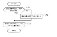
次に、図22を参照して、本実施の形態にかかるDRAMアクセス部32におけるDRAM書込動作について説明する。図22は、DRAM書込処理を示すフローチャートである。
DRAMアクセス部32は、書込制御部34からのDRAM書込指示に応じて、図22のDRAM書込処理を実行する。[DRAM write operation]
Next, with reference to FIG. 22, a DRAM write operation in the
The
まず、活性化処理部32Bは、FIFOメモリ32Aに蓄積されたDRAM書込指示で指定された書込対象ロウアドレスが活性化状態にあるか確認し(ステップ170)、書込対象ロウアドレスが活性化状態にない場合は(ステップ170:NO)、書込対象ロウアドレスの活性化を行って(ステップ171)、活性化処理を完了する。なお、書込対象ロウアドレスが活性化状態にある場合(ステップ170:YES)、何もせず活性化処理を完了する。 First, the
活性化処理部32Bでの活性化処理を完了後、DRAM書込指示はFIFOメモリ32Aから出力され、アクセス種別判定部32Cを介してDRAM書込部32Dに入力される。
これに応じて、DRAM書込部32Dは、入力されたDRAM書込指示に対応するコラムアドレスに、DRAM書込指示で指定されたフレームデータ(データD)を書き込んだ後(ステップ172)、一連のDRAM書込処理を終了する。After completing the activation processing in the
In response, the
本実施の形態では、データメモリ31を構成するDRAMにフレームデータを書き込む際、書込制御部34により、DRAMが持つ各バンクのうちから、書込対象ロウアドレスが活性化状態にあるバンクが書込対象バンクとして優先的に選択される。これにより、同一バンクの異なるロウアドレスへの書き込みが発生する確率が低減されることになる。このため、フレームデータ書込時におけるロウアドレスの活性化や、異なるロウアドレスに対するアクセス完了を待つ回数が削減されることになり、DRAMアクセスの実効スループットの低下が抑制される。 In this embodiment, when writing frame data to the DRAM constituting the
[DRAM読出動作]
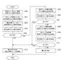
次に、図23を参照して、本実施の形態にかかるDRAMアクセス部32におけるDRAM読出動作について説明する。図23は、DRAM読出処理を示すフローチャートである。
DRAMアクセス部32は、読出制御部35からのDRAM読出指示に応じて、図23のDRAM読出処理を実行する。[DRAM read operation]
Next, with reference to FIG. 23, a DRAM read operation in the
The
まず、活性化処理部32Bは、FIFOメモリ32Aに蓄積されたDRAM読出指示で指定された読出対象バンクにおいて、読出対象ロウアドレスが活性化状態にあるか確認し(ステップ180)、読出対象ロウアドレスが活性化状態にある場合(ステップ180:YES)、何もせず活性化処理を完了する。 First, the
活性化処理部32Bでの活性化処理を完了後、DRAM読出指示はFIFOメモリ32Aから出力され、アクセス種別判定部32Cを介してDRAM読出部32Eに入力される。
これに応じて、DRAM読出部32Eは、入力されたDRAM読出指示に対応する読出対象バンクの読出対象ロウアドレスのうち、指示されたコラムアドレスからフレームデータ(データD)を読み出した後(ステップ184)、DRAM読出処理を終了する。After completing the activation process in the
In response, DRAM read
また、読出対象バンクの読出対象ロウアドレスが活性化状態にない場合(ステップ180:NO)、活性化処理部32Bは、読出対象バンクにおいて異なるロウアドレスが活性化状態にあるか確認する(ステップ181)。
ここで、異なるロウアドレスが活性化状態にない場合(ステップ181:NO)、活性化処理部32Bは、読出対象バンクの読出対象ロウアドレスを活性化し(ステップ183)、活性化処理を完了する。これにより、DRAM読出部32Eにおいて、活性化された読出対象ロウアドレスからの読み出しが行われることになる。If the read target row address of the read target bank is not in the activated state (step 180: NO), the
If a different row address is not in the activated state (step 181: NO), the
また、異なるロウアドレスが活性化状態にある場合(ステップ181:YES)、活性化処理部32Bは、異なるロウアドレスへのアクセスが完了するまで待機した後(ステップ182)、ステップ183へ移行して、前述と同様に読出対象ロウアドレスの活性化を行う。 If a different row address is in the activated state (step 181: YES), the
このように、データメモリ31を構成するDRAMからフレームデータを読み出す際、読出対象となるフレームデータが特定のバンクに書き込まれていることから、書き込み時のように、ロウアドレスが活性化状態にあるバンクを選択することはできない。このため、同一バンクの異なるロウアドレスからの読み出しや、書き込み後の同一バンクからの読み出しにおいて待ち時間が発生するものとなる。なお、同一バンクの異なるロウアドレスからの読み出しについては、異なるロウアドレスからの読み出しが連続しないように、例えば、両者の間に書き込みが挿入されるよう処理間隔をあけるようにしてもよい。 As described above, when reading frame data from the DRAM constituting the
[第1の実施の形態の効果]
このように、本実施の形態は、記録装置30において、データメモリ31をバンクごとにライトポインタを有するDRAMから構成して、バンクごとにライトポインタのロウアドレスが活性化状態であるか否かを示す活性化状態フラグを記憶するキュー制御メモリ33を備え、書込対象キューにフレームデータを書き込む際、バンクのうち活性化状態フラグが活性化状態であることを示しているバンクを書込対象バンクとして選択して当該フレームデータを書き込み、活性化状態フラグが活性化状態であることを示しているバンクが存在しない場合は、活性化状態フラグが非活性化状態であることを示しているバンクを書込対象バンクとして選択して当該バンクのライトポインタのロウアドレスを活性化した後に当該フレームデータを書き込むようにしたものである。[Effect of the first embodiment]
As described above, according to the present embodiment, in the
一般に、DRAMでは、任意のバンクの任意のロウアドレスにデータを書き込む場合、当該バンクにおいて当該ロウアドレスを活性化する必要があり、同一バンクの異なるロウアドレスにアクセスする場合には、当該ロウアドレスを用いたアクセスが完了するのを待ってから、新たなロウアドレスを活性化する必要があるため、同一バンクへのアクセスにおいて、ロウアドレスの活性化に起因して比較的大きな待ち時間が発生する。具体的には、同一バンクの異なるロウアドレスへのアクセスが連続した場合である。その他に待ち時間が発生する条件として、読み出し後の同一バンクに書き込みを行う場合、および、書き込み後の同一バンクから読み出しを行う場合がある。 In general, in a DRAM, when writing data to an arbitrary row address of an arbitrary bank, it is necessary to activate the row address in the bank. When accessing a different row address of the same bank, the row address is Since it is necessary to activate a new row address after waiting for the used access to be completed, a relatively large waiting time occurs due to the activation of the row address in accessing the same bank. Specifically, this is a case where accesses to different row addresses in the same bank are continuous. As other conditions for waiting time, there are a case where writing is performed in the same bank after reading and a case where reading is performed from the same bank after writing.
本実施形態によれば、データメモリ31を構成するDRAMにフレームデータを書き込む際、DRAMが持つ各バンクのうちから、活性化状態フラグが活性化状態であることを示しているバンクが書込対象バンクとして優先的に選択される。
これにより、同一バンクの異なるロウアドレスへの書き込みが発生する確率を低減することができる。したがって、フレームデータ書込時におけるロウアドレスの活性化や、異なるロウアドレスに対するアクセス完了を待つ回数を低減させることができ、DRAMアクセスに関する実効スループットの低下を抑制し、活性化処理に起因する電力消費を削減することが可能となる。According to the present embodiment, when writing the frame data to the DRAM constituting the
This can reduce the probability of writing to different row addresses in the same bank. Therefore, it is possible to reduce the number of times of waiting for the activation of the row address at the time of writing the frame data and the completion of the access to the different row address, suppressing the decrease in the effective throughput related to the DRAM access, and the power consumption caused by the activation process. Can be reduced.
また、本実施の形態において、記録装置30において、仮想格納アドレスごとに、当該仮想格納アドレスに書き込まれた通信データに後続する通信データの仮想格納アドレスを示す後続アドレスを記憶し、キューごとに、当該キューの通信データが書き込まれている仮想格納アドレスの先頭および最終を示すキュー先頭アドレスおよびキュー最終アドレスを記憶し、各キューに共通して、次に通信データを書き込むべき仮想格納アドレスを示す次書込アドレスをバンクごとに記憶するようにしてもよい。 In the present embodiment, the
これに加えて、書込制御部34が、書込対象キューに通信データを書き込む(書き込み指示を行う)際、選択されたバンクの次書込アドレスからなる書込対象仮想アドレスに当該通信データを書き込み、当該書込対象キューのキュー最終アドレス、書込前のキュー最終アドレスに関する後続仮想アドレス、および選択されたバンクの次書込アドレスをそれぞれ更新し、読出制御部35が、読出対象キューから通信データを読み出す(読み出し指示を行う)際、当該読出対象キューのキュー先頭アドレスからなる読出対象仮想アドレス(バンク情報を含む)から当該通信データを読み出し、当該読出対象キューのキュー先頭アドレス、読出対象バンクの次書込アドレス、および新たな次書込アドレス(読出対象バンク用)に関する後続仮想アドレスをそれぞれ更新するようにしてもよい。 In addition to this, when the
これにより、各キューのフレームデータが、空き状態にある仮想格納アドレスに順次書き込まれ、フレームデータが読み出された仮想格納アドレスが再び空き状態として管理されることになる。またキューごとに書き込まれた順序でフレームデータの仮想格納アドレスが管理されることになる。空き状態にある仮想格納アドレスについては、複数のキューで共用することができ、従来のキューごとに予めアドレス範囲を固定的に確保しておく場合と比較して、メモリの使用効率を高めることが可能となる。このため、メモリ容量の増大を行う必要がなくなり、結果として回路規模やコストの増大を抑制することが可能となる。 As a result, the frame data of each queue is sequentially written to the virtual storage address in the free state, and the virtual storage address from which the frame data has been read out is managed again as a free state. Further, the virtual storage address of the frame data is managed in the order of writing for each queue. A virtual storage address in an empty state can be shared by a plurality of queues, and the use efficiency of the memory can be improved as compared with a case where a fixed address range is secured in advance for each conventional queue. It becomes possible. For this reason, it is not necessary to increase the memory capacity, and as a result, an increase in circuit scale and cost can be suppressed.
また、本実施の形態において、書込制御部34が書込対象として選択されたバンクの次書込アドレスを更新する際に、書込対象バンクの書込対象仮想アドレスに対応する現在のライトポインタのロウアドレスと更新後の次書込アドレスに対応する更新後のライトポインタのロウアドレスが同じ場合は書込対象バンクの活性化状態フラグを活性化状態であることを示す値とし、ロウアドレスが異なる場合はフラグを非活性化状態とするようにしてもよい。 In the present embodiment, when the
また、読出制御部35が読出対象バンクの次書込アドレス更新する際に、読出対象バンクの読出対象仮想アドレスに対応するリードポインタのロウアドレスと更新後の次書込アドレスに対応する更新後のライトポインタのロウアドレスが同じ場合は読出対象バンクの活性化状態フラグを活性化状態であることを示す値とし、ロウアドレスが異なる場合はフラグを非活性化状態とするようにしてもよい。 Further, when the
これに加えて、直近n回分の書込または読出対象となったアドレスからなるアクセス履歴を記憶し、書込制御部34が、書込対象キューへの書き込み指示を行う際、および、読出制御部35が、読出対象キューからの読み出し指示を行う際に、書込または読出対象仮想アドレスをアクセス履歴に追加してもよい。 In addition to this, an access history consisting of addresses that have been subjected to writing or reading for the latest n times is stored, and when the
これにより、活性化状態フラグが活性化状態であることを示しているバンクが存在しない場合でも、先行の書き込み・読み出しが既に完了しているバンク、あるいは、先行の書き込み・読み出しが最も早く完了するバンクがわかることになる。その結果、活性化処理をすぐに開始できるバンク、または、最も早く活性化処理を開始できるバンクを選択して書き込み指示を行うことにより、DRAMアクセスに関する実効スループットの低下を抑制することが可能となる。 As a result, even when there is no bank indicating that the activation state flag is in the activated state, the preceding writing / reading is completed or the preceding writing / reading is completed earliest. You will know the bank. As a result, it is possible to suppress a decrease in effective throughput related to DRAM access by selecting a bank that can start the activation process immediately or a bank that can start the activation process earliest. .
また、アクセス履歴に残っている範囲に限り、活性化状態フラグが活性化状態であることを示しているバンクが複数ある場合において、最も後に書込指示または読出指示を行ったバンクがわかることになる。その結果、1個のフレームデータから1仮想アドレス分のデータサイズに合わせて分割された複数のデータDを同一バンクの同一ロウアドレスに書き込むことが可能となる。 Further, only in the range remaining in the access history, when there are a plurality of banks in which the activation state flag indicates the activated state, it is possible to know the bank that has performed the write instruction or the read instruction most recently. Become. As a result, it is possible to write a plurality of data D divided from one frame data according to the data size of one virtual address to the same row address of the same bank.
また、本実施の形態は、QM内のADD値等の初期値を設定する必要が無いという特徴がある。本実施の形態において、通信用入出力装置1の起動時に初期値を設定する必要がある情報はVAR、UAR、AARと、AFRのみである(図13の「Initialization」を参照)。従って、初期設定を行うための回路の規模、もしくは、初期設定を行うためのソフトウエアの規模が極めて小さく、初期設定に要する時間も極めて小さいという効果が有る。
なお、図13等において、EoF値格納用のPNをQM内に搭載する場合を例示しているが、PNをDRAM内に搭載することも可能である。In addition, this embodiment has a feature that it is not necessary to set an initial value such as an ADD value in the QM. In the present embodiment, only the VAR, UAR, AAR, and AFR information that need to set initial values when the communication input /
In FIG. 13 and the like, the case where the PN for storing the EoF value is mounted in the QM is illustrated, but it is also possible to mount the PN in the DRAM.
[第2の実施の形態]
次に、図24を参照して、本発明の第2の実施の形態にかかる通信用入出力装置1について説明する。図24は、第2の実施の形態にかかるアクセス調停部の構成を示すブロック図である。[Second Embodiment]
Next, with reference to FIG. 24, a communication input /
第1の実施の形態にかかる通信用入出力装置1において、仮想データメモリの仮想格納アドレスを複数のキューで共用するようにした際に、例えば、特定の出力系統に関するフレームデータが多量に入力された場合、仮想データメモリの仮想格納アドレスが当該出力系統のキューにより占有されてしまうという場合がある。このような格納アドレスの占有は、第1の実施の形態に限定されるものではなく、格納アドレスを複数のキューで共用する構成であれば、いずれの構成であっても発生しうる。したがって、このような格納アドレスの占有が発生した場合、他の出力系統のキューが十分な格納アドレス数を使用できず、フレームデータの破棄が発生しやすくなり、通信品質が劣化する原因となる。 In the communication input /
本実施の形態は、このような複数のキューによる格納アドレスの共用時における、特定キューによる格納アドレスの占有を回避することを目的とし、記録装置30において、アクセス調停部37が、書込対象キューにフレームデータを書き込む(書き込み指示を行う)際、当該フレームデータのデータ長に基づき、書き込みに必要となる仮想格納アドレスの数を示す必要アドレス数を算出し、キュー使用アドレス数メモリ36から取得した当該書込対象キューまたは各キューの使用仮想アドレス数に基づき、当該書き込みに使用可能な仮想格納アドレスの数を示す残り仮想アドレス数を算出し、当該必要アドレス数と当該残り仮想アドレス数とを比較することにより当該フレームデータの書込可否を判定し、書込可の判定に応じて書込制御部34に対して当該フレームデータの書き込みを指示するようにしたものである。 The purpose of this embodiment is to avoid occupying a storage address by a specific queue when the storage address is shared by a plurality of queues. In the
図24に示すように、本実施の形態において、アクセス調停部37には、主な回路部として、書込可否判定部37A、書込用FIFO37B、読出受付部37C、読出用FIFO37D、優先制御部37E、キュー使用アドレス数更新部37F、および指示出力部37Gが設けられている。 As shown in FIG. 24, in the present embodiment, the
書込可否判定部37Aは、多重化装置10から転送されたフレームデータに付加されているキュー指定情報およびフレーム長情報と、キューごとに予め設定されている判定用アドレス数情報と、各キューの使用仮想アドレス数とに基づいて、書込可能か否か判定する機能と、書込可の判定結果に応じて、当該フレームデータを、データメモリ31に設けられている格納領域の1仮想アドレス分のデータサイズに分割し、得られたデータにキュー指定情報を付加した書き込み指示を、それぞれ書込用FIFO37Bに書き込む機能とを有している。 The write enable / disable determining
判定用アドレス数情報には、当該キュー指定情報で指定された書込対象キューで使用可能な最大仮想アドレス数NKmaxと、当該書込対象キューに対して使用が保証されている最低保証仮想アドレス数NKminとが含まれている。
図25は、判定用アドレス数情報の構成例である。ここではキューを識別するためのキューIDごとに、最大仮想アドレス数NKmaxと最低保証仮想アドレス数NKminとが設定されている。これら判定用アドレス数情報は、例えばキュー使用アドレス数更新部37F、あるいはアクセス調停部37の内部メモリ(図示せず)で記憶されている。The determination address number information includes the maximum number of virtual addresses NKmax that can be used in the write target queue specified by the queue specification information, and the minimum guaranteed virtual address number that is guaranteed to be used for the write target queue. NKmin.
FIG. 25 is a configuration example of the determination address number information. Here, for each queue ID for identifying a queue, a maximum virtual address number NKmax and a minimum guaranteed virtual address number NKmin are set. The determination address number information is stored in, for example, the queue use address
読出受付部37Cは、多重分離装置20から出力された読み出し要求の読出データ量情報に基づいて、データメモリ31に対する読み出し回数を計算し、その読み出し回数だけ当該読み出し要求のキュー指定情報を読み出し指示として読出用FIFO37Dに書き込む機能を有している。この計算は、読出データ量情報が示すデータ量をデータメモリ31の1仮想アドレスあたりのデータサイズで除算した値を読み出し回数とし、剰余がある場合は読み出し回数に1を加算すればよい。 The
優先制御部37Eは、書込用FIFO37Bもしくは読出用FIFO37Dから、書き込み指示もしくは読み出し指示を読み出して、キュー使用アドレス数更新部37Fへ出力する機能と、書込用FIFO37Bと読出用FIFO37Dの双方に、書き込み指示と読み出し指示が存在する場合は、書込用FIFO37Bからの書き込み指示を優先して読み出す機能とを有している。 The
キュー使用アドレス数更新部37Fは、優先制御部37Eから書き込み指示が入力された場合は、キュー使用アドレス数メモリ36のうち、当該書き込み指示のキュー指定情報と対応する書込対象キューの使用仮想アドレス数に1を加算し、当該書き込み指示を指示出力部37Gへ出力する機能と、優先制御部37Eから読み出し指示が入力された場合は、キュー使用アドレス数メモリ36のうち、当該読み出し指示のキュー指定情報と対応する読出対象キューの使用仮想アドレス数から1を減算し、当該読み出し指示を指示出力部37Gへ出力する機能とを有している。 When a write instruction is input from the
指示出力部37Gは、キュー使用アドレス数更新部37Fから書き込み指示が入力された場合は、当該書き込み指示を書込制御部34へ出力する機能と、読み出し指示が入力された場合は、当該読み出し指示を読出制御部35へ出力する機能とを有している。 The
[第2の実施の形態の動作]
次に、図26を参照して、本実施の形態にかかるアクセス調停部37の動作として、フレームデータの書き込み時における書込判定動作について説明する。図26は、第2の実施の形態にかかる書込可否判定処理を示すフローチャートである。
記録装置30のアクセス調停部37は、多重化装置10から転送されたフレームデータごとに、図26の書込可否判定処理に基づいて、書込可否を判定する。[Operation of Second Embodiment]
Next, with reference to FIG. 26, a write determination operation at the time of writing frame data will be described as the operation of the
The
まず、アクセス調停部37は、キュー使用アドレス数メモリ36から全キューに関する使用仮想アドレス数NKを取得して(ステップ200)、全キューが使用している合計仮想アドレス数NKAを算出し(ステップ201)、書込対象となる対象フレームデータの書き込みに要する必要仮想アドレス数NFを算出する(ステップ202)。 First, the
この後、仮想データメモリの仮想格納アドレスの総アドレス数NAからNKAを減算することにより、対象フレームデータの書き込みに使用可能な仮想格納アドレスの数を示す残り仮想アドレス数NRを算出し(ステップ203)、NFとNRとを比較する(ステップ204)。
ここで、NF>NRの場合(ステップ204:YES)、アクセス調停部37は、書込不可と判定して対象フレームデータを破棄し(ステップ213)、当該対象フレームデータに関する書込判定処理を終了する。Thereafter, by subtracting NKA from the total address number NA of the virtual storage addresses of the virtual data memory, the remaining virtual address number NR indicating the number of virtual storage addresses that can be used for writing the target frame data is calculated (step 203). ), NF and NR are compared (step 204).
Here, when NF> NR (step 204: YES), the
一方、NF≦NRの場合(ステップ204:NO)、アクセス調停部37は、指定された書込対象キューの最大仮想アドレス数NKmaxをキュー使用アドレス数メモリ36等から取得して(ステップ205)、NKmaxからNKを減算することにより残り仮想アドレス数NRを算出し(ステップ206)、NFとNRとを比較する(ステップ207)。
ここで、NF>NRの場合(ステップ207:YES)、アクセス調停部37は、書込不可と判定して対象フレームデータを破棄し(ステップ213)、当該対象フレームデータに関する書込判定処理を終了する。On the other hand, when NF ≦ NR (step 204: NO), the
Here, when NF> NR (step 207: YES), the
一方、NF≦NRの場合(ステップ207:NO)、アクセス調停部37は、全キューに関する最低保証仮想アドレス数NKminをキュー使用アドレス数メモリ36から取得し(ステップ208)、全キューを一括して最低限保証すべき総保証仮想アドレス数NAminを算出する(ステップ209)。この際、任意のキューのキュー使用仮想アドレス数NKがその最低保証仮想アドレス数以上である場合は、当該キューの保証仮想アドレス数としてキュー使用仮想アドレス数NKを加算し、キュー使用仮想アドレス数NKがその最低保証仮想アドレス数未満である場合は、当該キューの保証仮想アドレス数として最低保証仮想アドレス数NKminを加算する。 On the other hand, when NF ≦ NR (step 207: NO), the
この後、アクセス調停部37は、NAからNAminを減算することにより残り仮想アドレス数NRを算出し(ステップ210)、NFとNRとを比較する(ステップ211)。
ここで、NF>NRの場合(ステップ211:YES)、アクセス調停部37は、書込不可と判定して対象フレームデータを破棄し(ステップ213)、当該対象フレームデータに関する書込判定処理を終了する。Thereafter, the
Here, if NF> NR (step 211: YES), the
一方、NF≦NRの場合(ステップ211:NO)、アクセス調停部37は、対象フレームデータについて書込可と判定し(ステップ212)、当該対象フレームデータに関する書込判定処理を終了する。
この後、この書込可の判定に応じて、アクセス調停部37は、対象フレームデータを1仮想アドレス分のデータサイズに分割し、得られたデータにキュー指定情報を付加した書き込み指示を、それぞれ書込用FIFO37Bに書き込むことになる。On the other hand, if NF ≦ NR (step 211: NO), the
Thereafter, the
[第2の実施の形態の効果]
このように、本実施の形態は、記録装置30において、キュー使用アドレス数メモリ36が、キューごとに、当該キューが使用している仮想格納アドレスの数を示す使用アドレス数を記憶し、アクセス調停部37が、書込対象キューに通信データを書き込む(書き込み指示を行う)際、当該通信データのデータ長に基づき、書き込みに必要となる仮想格納アドレスの数を示す必要アドレス数を算出し、キュー使用アドレス数メモリ36から取得した当該書込対象キューまたは各キューの使用仮想アドレス数等に基づき、当該書き込みに使用可能な仮想格納アドレスの数を示す残り仮想アドレス数を算出し、当該必要アドレス数と当該残り仮想アドレス数とを比較することにより当該通信データの書込可否を判定し、書込可の判定に応じて書込制御部34に対して当該通信データの書き込みを指示するようにしたものである。[Effect of the second embodiment]
As described above, according to the present embodiment, in the
したがって、それぞれのキューによる仮想格納アドレスの使用数が制限されるため、任意の出力系統と対応するキューによる仮想格納アドレスの占有を抑止することができる。このため、特定の出力系統に関するフレームデータが多量に入力された場合でも、他の出力系統のキューが十分な仮想格納アドレス数を使用することが可能となる。これにより、フレームデータの破棄やこれによる通信品質の劣化を抑制することが可能となるとともに、これら対策として、メモリ容量の増大を行う必要がなくなり、結果として回路規模やコストの増大を抑制することが可能となる。 Therefore, since the number of virtual storage addresses used by each queue is limited, occupation of the virtual storage address by a queue corresponding to an arbitrary output system can be suppressed. For this reason, even when a large amount of frame data related to a specific output system is input, it is possible for the queues of other output systems to use a sufficient number of virtual storage addresses. As a result, it becomes possible to suppress the discarding of frame data and the deterioration of communication quality due to this, and as a countermeasure, it is not necessary to increase the memory capacity, and as a result, the increase in circuit scale and cost is suppressed. Is possible.
なお、本実施の形態におけるNKA及びNAminの算出は、キュー使用アドレス数メモリ36を更新する際に同時に算出(加算、減算等)することができる。
本実施の形態において、図24の構成のアクセス調停部37を用いる場合、書込用FIFO37Bに書き込み指示データが存在していると誤って書込可能と判定してしまう可能性がある。誤った判定を防止するためには、各キューの使用仮想アドレス数としてキュー使用アドレス数メモリ36の情報に書込用FIFO37B内の仮想アドレス数(書き込み指示の数)を加算した値を使用するか、NAもしくはNKmaxとして書込用FIFO37B内の仮想アドレス数(書き込み指示の数)を減算した値を使用すればよい。Note that NKA and NAmin in this embodiment can be calculated (added, subtracted, etc.) at the same time when the queue use
In the present embodiment, when the
[実施の形態の拡張]
以上、実施形態を参照して本発明を説明したが、本発明は上記実施形態に限定されるものではない。本発明の構成や詳細には、本発明のスコープ内で当業者が理解しうる様々な変更をすることができる。また、各実施形態については、矛盾しない範囲で任意に組み合わせて実施することができる。[Extended embodiment]
The present invention has been described above with reference to the embodiments, but the present invention is not limited to the above embodiments. Various changes that can be understood by those skilled in the art can be made to the configuration and details of the present invention within the scope of the present invention. In addition, each embodiment can be implemented in any combination within a consistent range.
上記の各実施の形態において、通信用入出力装置1でマルチキャストフレームを処理する場合、出力系統の1つとしてマルチキャスト用出力系統を設けるとともに多重分離装置20内の振分部22にマルチキャストフレームを複数の速度変換部23に出力する手段を設け、記録装置30のデータメモリ31内に論理的に形成した一部のキューをこのマルチキャスト用出力系統に対応するキューとして割り当てるようにしてもよい。
これにより、外部から多重化装置10に入力されたマルチキャストフレームが、データメモリ31内のマルチキャスト用出力系統に対応するキューに一時格納され、当該キューから多重分離装置20によりマルチキャストフレームが読み出されて複数の出力ポートから出力される。In each of the above embodiments, when the communication input /
As a result, the multicast frame input from the outside to the
1…通信用入出力装置、10…多重化装置、11…キュー指定情報付加部、12…多重化部、20…多重分離装置、21…読出部、22…振分部、23,24…速度変換部、30…記録装置、31…データメモリ、32…DRAMアクセス部、32A…FIFOメモリ、32B…活性化処理部、32C…アクセス種別判定部、32D…DRAM書込部、32E…DRAM読出部、33…キュー制御メモリ、34…書込制御部、35…読出制御部、36…キュー使用アドレス数メモリ、37…アクセス調停部、37A…書込可否判定部、37B…書込用FIFO、37C…読出受付部、37D…読出用FIFO、37E…優先制御部、37F…キュー使用アドレス数更新部、37G…指示出力部。 DESCRIPTION OF
Claims (3)
Translated fromJapanese前記記録装置は、
バンクごとにライトポインタを有するDRAMからなり、前記キューの通信データを記憶する前記データメモリと、
前記バンクごとに前記ライトポインタのロウアドレスが活性化状態であるか否かを示す活性化状態フラグを記憶するキュー制御メモリと、
前記書込対象キューに前記通信データを書き込む際、前記バンクのうち活性化状態フラグが活性化状態であることを示しているバンクを書込対象バンクとして選択して当該通信データを書き込み、活性化状態フラグが活性化状態であることを示しているバンクが存在しない場合は、活性化状態フラグが非活性化状態であることを示しているバンクを書込対象バンクとして選択して当該バンクのライトポインタのロウアドレスを活性化した後に当該通信データを書き込むDRAMアクセス部と
を備えることを特徴とする通信用入出力装置。A multiplexing device that multiplexes by adding queue designation information indicating a queue corresponding to an output system to which the communication data is to be output, and the communication data transferred from the multiplexing device. Corresponding to a recording device for temporarily storing in a queue to be written designated by the queue designation information among a plurality of queues logically formed in the data memory, and an output system selected based on the priority control logic among the queues A communication input / output device comprising: a demultiplexer that reads the communication data from the read target queue and converts the communication data into a communication speed of an output port corresponding to the output system;
The recording device includes:
The data memory, which comprises a DRAM having a write pointer for each bank, stores communication data of the queue,
A queue control memory for storing an activation state flag indicating whether or not the row address of the write pointer is activated for each bank;
When writing the communication data to the write target queue, the bank indicating that the activation state flag is in the active state among the banks is selected as the write target bank, and the communication data is written and activated. If there is no bank indicating that the status flag is in the activated state, the bank indicating that the activated state flag is in the inactivated state is selected as the write target bank, and the bank is written. And a DRAM access unit for writing the communication data after activating the row address of the pointer.
前記記録装置は、
前記キュー制御メモリのキュー制御情報に基づいて、前記多重化装置から転送された前記通信データの前記書込対象キューに対する書き込みを前記DRAMアクセス部に指示する書込制御部と、
前記キュー制御メモリのキュー制御情報に基づいて、前記読出対象キューからの通信データの読み出しを前記DRAMアクセス部に指示し、読み出した通信データを前記多重分離装置へ転送する読出制御部とをさらに備え、
前記キュー制御メモリは、前記活性化状態フラグを前記バンクごとに記憶するとともに、仮想データメモリ上で用いられる仮想格納アドレスごとに、当該仮想格納アドレスに書き込まれた通信データに後続する通信データの仮想格納アドレスを示す後続アドレスを記憶し、前記キューごとに、当該キューの通信データが書き込まれている前記仮想格納アドレスの先頭および最終を示すキュー先頭アドレスおよびキュー最終アドレスを記憶し、前記キューのそれぞれに共通して、前記ライトポインタとバンクごとに1対1に対応して次に通信データを書き込むべき仮想格納アドレスを示すバンクごとの次書込アドレスを記憶し、
前記書込制御部は、前記書込対象キューに前記通信データを書き込む際、前記書込対象バンクとして選択したバンクの前記次書込アドレスからなる書込対象仮想アドレスに対する当該通信データの書き込みをDRAMアクセス部に指示し、当該書込対象キューのキュー最終アドレス、書込前のキュー最終アドレスに関する後続アドレス、および書込対象バンクとして選択したバンクの次書込アドレスをそれぞれ更新し、前記書込対象バンクの書込対象仮想アドレスに対応する現在のライトポインタのロウアドレスと更新後の次書込アドレスに対応する更新後のライトポインタのロウアドレスとが同じ場合は、前記書込対象バンクの活性化状態フラグを活性化状態であることを示す値とし、前記ロウアドレスが互いに異なる場合は、前記活性化状態フラグを非活性化状態とし、
前記読出制御部は、前記読出対象キューから前記通信データを読み出す際、当該読出対象キューのキュー先頭アドレスからなる読出対象仮想アドレスに対する当該通信データの読み出しをDRAMアクセス部に指示し、当該読出対象キューのキュー先頭アドレス、読出対象バンクの次書込アドレス、および新たな読出対象バンクの次書込アドレスに関する後続アドレスをそれぞれ更新し、前記読出対象バンクの読出対象仮想アドレスに対応するリードポインタのロウアドレスと更新後の次書込アドレスに対応する更新後のライトポインタのロウアドレスとが同じ場合は、前記読出対象バンクの活性化状態フラグを活性化状態であることを示す値とし、前記ロウアドレスが互いに異なる場合は、前記活性化状態フラグを非活性化状態とする
ことを特徴とする通信用入出力装置。The communication input / output device according to claim 1,
The recording device includes:
A write control unit that instructs the DRAM access unit to write the communication data transferred from the multiplexing device to the write target queue based on queue control information in the queue control memory;
A read control unit that instructs the DRAM access unit to read communication data from the read target queue based on queue control information in the queue control memory, and transfers the read communication data to the demultiplexer; ,
The queue control memory stores the activation state flag for each bank, and for each virtual storage address used on the virtual data memory, virtual communication data following the communication data written to the virtual storage address is stored. A subsequent address indicating a storage address is stored, and for each of the queues, a queue start address and a queue end address indicating the start and end of the virtual storage address in which communication data of the queue is written are stored. In common, the next write address for each bank indicating a virtual storage address to which communication data is to be written next is stored in correspondence with each of the write pointer and each bank,
When the write control unit writes the communication data to the write target queue, the write control unit writes the communication data to the write target virtual address including the next write address of the bank selected as the write target bank. The access unit is instructed to update the queue last address of the write target queue, the subsequent address related to the queue final address before writing, and the next write address of the bank selected as the write target bank, respectively. If the current write pointer row address corresponding to the write target virtual address of the bank is the same as the updated write pointer row address corresponding to the updated next write address, the write target bank is activated. When the status flag is a value indicating an activated state and the row addresses are different from each other, the activated The status flag is set to the inactive state,
When reading the communication data from the read target queue, the read control unit instructs the DRAM access unit to read the communication data for the read target virtual address consisting of the queue head address of the read target queue, and The queue start address, the next write address of the read target bank, and the subsequent address related to the next write address of the new read target bank are updated, and the row address of the read pointer corresponding to the read target virtual address of the read target bank is updated. When the row address of the updated write pointer corresponding to the updated next write address is the same, the activation state flag of the bank to be read is set to a value indicating the activated state, and the row address is If they are different from each other, the activated state flag should be deactivated. An input / output device for communication.
前記記録装置は、
前記キューごとに、当該キューが使用している前記仮想データメモリ上での仮想格納アドレスの数を示す使用アドレス数を記憶するキュー使用アドレス数メモリと、
前記書込対象キューに前記通信データを書き込む際、当該通信データのデータ長に基づき、書き込みに必要となる仮想格納アドレスの数を示す必要アドレス数を算出し、前記キュー使用アドレス数メモリから取得した当該書込対象キューまたは前記キューの使用アドレス数に基づき、当該書き込みに使用可能な仮想格納アドレスの数を示す残りアドレス数を算出し、当該必要アドレス数と当該残りアドレス数とを比較することにより当該通信データの書込可否を判定し、書込可の判定に応じて当該通信データの書き込みを指示するアクセス調停部と
をさらに備えることを特徴とする通信用入出力装置。The communication input / output device according to claim 1 or 2,
The recording device includes:
A queue use address number memory for storing a use address number indicating the number of virtual storage addresses on the virtual data memory used by the queue for each queue;
When writing the communication data to the write target queue, the necessary address number indicating the number of virtual storage addresses required for writing is calculated based on the data length of the communication data, and obtained from the queue use address number memory By calculating the number of remaining addresses indicating the number of virtual storage addresses that can be used for the writing based on the number of addresses used in the writing target queue or the queue, and comparing the number of necessary addresses with the number of remaining addresses An communication input / output device, further comprising: an access arbitration unit that determines whether or not the communication data can be written, and instructs writing of the communication data in accordance with the determination of whether or not the communication data can be written.
Priority Applications (3)
| Application Number | Priority Date | Filing Date | Title |
|---|---|---|---|
| JP2018096925AJP2019204150A (en) | 2018-05-21 | 2018-05-21 | Input-output apparatus for communication |
| PCT/JP2019/018560WO2019225336A1 (en) | 2018-05-21 | 2019-05-09 | Communication input-output device |
| US17/057,055US11546276B2 (en) | 2018-05-21 | 2019-05-09 | Communication input-output device |
Applications Claiming Priority (1)
| Application Number | Priority Date | Filing Date | Title |
|---|---|---|---|
| JP2018096925AJP2019204150A (en) | 2018-05-21 | 2018-05-21 | Input-output apparatus for communication |
Publications (1)
| Publication Number | Publication Date |
|---|---|
| JP2019204150Atrue JP2019204150A (en) | 2019-11-28 |
Family
ID=68615854
Family Applications (1)
| Application Number | Title | Priority Date | Filing Date |
|---|---|---|---|
| JP2018096925APendingJP2019204150A (en) | 2018-05-21 | 2018-05-21 | Input-output apparatus for communication |
Country Status (3)
| Country | Link |
|---|---|
| US (1) | US11546276B2 (en) |
| JP (1) | JP2019204150A (en) |
| WO (1) | WO2019225336A1 (en) |
Cited By (1)
| Publication number | Priority date | Publication date | Assignee | Title |
|---|---|---|---|---|
| JP2022046413A (en)* | 2020-09-10 | 2022-03-23 | ウェスタン デジタル テクノロジーズ インコーポレーテッド | Enhanced read-ahead capability for storage devices |
Citations (4)
| Publication number | Priority date | Publication date | Assignee | Title |
|---|---|---|---|---|
| JP2016158024A (en)* | 2015-02-23 | 2016-09-01 | 日本電信電話株式会社 | Communication input / output device |
| JP2016157284A (en)* | 2015-02-25 | 2016-09-01 | 日本電信電話株式会社 | Communication input / output device |
| JP2018032129A (en)* | 2016-08-23 | 2018-03-01 | 日本電信電話株式会社 | Input/output device for communication |
| JP2018032925A (en)* | 2016-08-23 | 2018-03-01 | 日本電信電話株式会社 | Communication input / output device |
Family Cites Families (9)
| Publication number | Priority date | Publication date | Assignee | Title |
|---|---|---|---|---|
| US5842033A (en)* | 1992-06-30 | 1998-11-24 | Discovision Associates | Padding apparatus for passing an arbitrary number of bits through a buffer in a pipeline system |
| US5889714A (en)* | 1997-11-03 | 1999-03-30 | Digital Equipment Corporation | Adaptive precharge management for synchronous DRAM |
| US6571323B2 (en)* | 1999-03-05 | 2003-05-27 | Via Technologies, Inc. | Memory-access management method and system for synchronous dynamic Random-Access memory or the like |
| US20040088472A1 (en)* | 2002-10-31 | 2004-05-06 | Nystuen John M. | Multi-mode memory controller |
| US7761656B2 (en)* | 2007-08-22 | 2010-07-20 | Advanced Micro Devices, Inc. | Detection of speculative precharge |
| US8151008B2 (en)* | 2008-07-02 | 2012-04-03 | Cradle Ip, Llc | Method and system for performing DMA in a multi-core system-on-chip using deadline-based scheduling |
| JP2011010195A (en) | 2009-06-29 | 2011-01-13 | Nippon Telegr & Teleph Corp <Ntt> | Input/output device for communication |
| US8576713B2 (en)* | 2010-04-23 | 2013-11-05 | Ixia | Traffic generator with priority flow control |
| US10320034B2 (en)* | 2017-03-03 | 2019-06-11 | The Boeing Company | Modular battery with battery cell and submodule interconnectivity |
- 2018
- 2018-05-21JPJP2018096925Apatent/JP2019204150A/enactivePending
- 2019
- 2019-05-09WOPCT/JP2019/018560patent/WO2019225336A1/ennot_activeCeased
- 2019-05-09USUS17/057,055patent/US11546276B2/enactiveActive
Patent Citations (4)
| Publication number | Priority date | Publication date | Assignee | Title |
|---|---|---|---|---|
| JP2016158024A (en)* | 2015-02-23 | 2016-09-01 | 日本電信電話株式会社 | Communication input / output device |
| JP2016157284A (en)* | 2015-02-25 | 2016-09-01 | 日本電信電話株式会社 | Communication input / output device |
| JP2018032129A (en)* | 2016-08-23 | 2018-03-01 | 日本電信電話株式会社 | Input/output device for communication |
| JP2018032925A (en)* | 2016-08-23 | 2018-03-01 | 日本電信電話株式会社 | Communication input / output device |
Cited By (2)
| Publication number | Priority date | Publication date | Assignee | Title |
|---|---|---|---|---|
| JP2022046413A (en)* | 2020-09-10 | 2022-03-23 | ウェスタン デジタル テクノロジーズ インコーポレーテッド | Enhanced read-ahead capability for storage devices |
| JP7170093B2 (en) | 2020-09-10 | 2022-11-11 | ウェスタン デジタル テクノロジーズ インコーポレーテッド | Improved read-ahead capabilities for storage devices |
Also Published As
| Publication number | Publication date |
|---|---|
| WO2019225336A1 (en) | 2019-11-28 |
| US20210184993A1 (en) | 2021-06-17 |
| US11546276B2 (en) | 2023-01-03 |
Similar Documents
| Publication | Publication Date | Title |
|---|---|---|
| CN102377682B (en) | Queue management method and device based on variable-length packets stored in fixed-size location | |
| US8225026B2 (en) | Data packet access control apparatus and method thereof | |
| US10740006B2 (en) | System and method for enabling high read rates to data element lists | |
| US8090921B2 (en) | Processing device, computer system, and mobile apparatus | |
| US9785367B2 (en) | System and method for enabling high read rates to data element lists | |
| US20170364291A1 (en) | System and Method for Implementing Hierarchical Distributed-Linked Lists for Network Devices | |
| JP6611011B2 (en) | Communication input / output device | |
| WO2019225336A1 (en) | Communication input-output device | |
| JP6570075B2 (en) | Communication input / output device | |
| US20070086428A1 (en) | Network packet storage method and network packet transmitting apparatus using the same | |
| JP6351073B2 (en) | Communication input / output device | |
| JP2016158024A (en) | Communication input / output device | |
| JP2019032699A (en) | Communication input / output device | |
| US7836231B2 (en) | Buffer control method and device thereof | |
| JP2019032727A (en) | Communication input / output device | |
| JP2019032705A (en) | Input/output device for communication | |
| US20170017568A1 (en) | System And Method For Implementing Distributed-Linked Lists For Network Devices | |
| US7529857B2 (en) | Data processing apparatus and data transfer control method | |
| JP2000299686A (en) | Scheduling device | |
| JP2014074993A (en) | Semiconductor device | |
| Wang et al. | Block-based packet buffer with deterministic packet departures | |
| EP3244582B1 (en) | Switch and data accessing method thereof | |
| US12417791B2 (en) | Direct memory access (DMA) circuit and operation method thereof | |
| JP2014194672A (en) | Memory control device and memory control method | |
| JP6212059B2 (en) | Communication input / output device |
Legal Events
| Date | Code | Title | Description |
|---|---|---|---|
| A621 | Written request for application examination | Free format text:JAPANESE INTERMEDIATE CODE: A621 Effective date:20200819 | |
| A131 | Notification of reasons for refusal | Free format text:JAPANESE INTERMEDIATE CODE: A131 Effective date:20210803 | |
| A521 | Request for written amendment filed | Free format text:JAPANESE INTERMEDIATE CODE: A523 Effective date:20211004 | |
| A02 | Decision of refusal | Free format text:JAPANESE INTERMEDIATE CODE: A02 Effective date:20220201 |