Movatterモバイル変換


[0]ホーム

URL:


JP2019192782A - Video display unit and video display device - Google Patents

Video display unit and video display device
Download PDF

Info

Publication number
JP2019192782A
JP2019192782AJP2018084070AJP2018084070AJP2019192782AJP 2019192782 AJP2019192782 AJP 2019192782AJP 2018084070 AJP2018084070 AJP 2018084070AJP 2018084070 AJP2018084070 AJP 2018084070AJP 2019192782 AJP2019192782 AJP 2019192782A
Authority
JP
Japan
Prior art keywords
package
video display
light emitting
covering member
circuit board
Prior art date
Legal status (The legal status is an assumption and is not a legal conclusion. Google has not performed a legal analysis and makes no representation as to the accuracy of the status listed.)
Granted
Application number
JP2018084070A
Other languages
Japanese (ja)
Other versions
JP7087630B2 (en
Inventor
聡 切通
Satoshi Kiridoori
聡 切通
斎藤 雄作
Yusaku Saito
雄作 斎藤
幹人 森部
Mikito Moribe
幹人 森部
寺西将人
Masato Teranishi
将人 寺西
Current Assignee (The listed assignees may be inaccurate. Google has not performed a legal analysis and makes no representation or warranty as to the accuracy of the list.)
Mitsubishi Electric Corp
Original Assignee
Mitsubishi Electric Corp
Priority date (The priority date is an assumption and is not a legal conclusion. Google has not performed a legal analysis and makes no representation as to the accuracy of the date listed.)
Filing date
Publication date
Application filed by Mitsubishi Electric CorpfiledCriticalMitsubishi Electric Corp
Priority to JP2018084070ApriorityCriticalpatent/JP7087630B2/en
Publication of JP2019192782ApublicationCriticalpatent/JP2019192782A/en
Application grantedgrantedCritical
Publication of JP7087630B2publicationCriticalpatent/JP7087630B2/en
Activelegal-statusCriticalCurrent
Anticipated expirationlegal-statusCritical

Links

Images

Landscapes

Abstract

Translated fromJapanese

【課題】従来よりも防水性能に優れた映像表示ユニット、及びその映像表示ユニットを備える映像表示装置を提供する。【解決手段】本発明に係る映像表示ユニットは、回路基板22と、回路基板22の上にマトリクス状に複数配置された発光装置と、回路基板22の上に形成されて回路基板22を被覆する被覆部材23とを備え、発光装置は、上面に凹部が形成されたパッケージ32と、凹部に配置された発光素子と、凹部に充填されており、発光素子が封止され、さらにパッケージ32の上面より盛り上がって形成された封止部材37とを有し、被覆部材23は、さらに、パッケージ32の側面、及びパッケージ32と封止部材37との境界面の外縁部51を被覆するものである。【選択図】図5PROBLEM TO BE SOLVED: To provide a video display unit having more excellent waterproof performance than ever, and a video display device provided with the video display unit. A video display unit according to the present invention includes a circuit board, a plurality of light emitting devices arranged in a matrix on the circuit board, and a circuit board formed on the circuit board to cover the circuit board. The light-emitting device includes a covering member 23, and the light-emitting device includes a package 32 having a recess formed in the upper surface, a light-emitting element disposed in the recess, and the light-emitting element filled in the recess, and the light-emitting element is sealed. The covering member 23 further covers the side surface of the package 32 and the outer edge portion 51 of the boundary surface between the package 32 and the sealing member 37. [Selection diagram] Fig. 5

Description

Translated fromJapanese

本発明は、映像表示ユニット、及び映像表示ユニットを備える映像表示装置に関する。  The present invention relates to a video display unit and a video display device including the video display unit.

映像表示装置は、道路近傍、スポーツ施設、建物壁等、屋外に設置され、映像を見る人物に種々の情報を提供する。映像表示装置は、マトリクス状に複数配置された映像表示ユニットを備える。  The video display device is installed outdoors such as in the vicinity of a road, a sports facility, a building wall, etc., and provides various information to a person watching the video. The video display device includes a plurality of video display units arranged in a matrix.

映像表示装置は、屋外に設置され、雨水にさらされる。そのため、映像表示ユニットに複数配置された発光装置には、防水性能が要求される。例えば、特許文献1には、発光装置へ電力を供給するリードフレームが防水用樹脂で被覆される構造が開示されている。  The video display device is installed outdoors and exposed to rainwater. Therefore, waterproof performance is required for a plurality of light emitting devices arranged in the video display unit. For example, Patent Document 1 discloses a structure in which a lead frame that supplies power to a light emitting device is covered with a waterproof resin.

特開2012−54533号公報JP 2012-54533 A

しかしながら、従来の映像表示ユニットでは、発光装置のパッケージと封止部材との境界面の外縁部から水が浸入する可能性があり、防水性能が十分ではないという課題があった。  However, the conventional video display unit has a problem that water may enter from the outer edge portion of the boundary surface between the light emitting device package and the sealing member, and the waterproof performance is not sufficient.

本発明は上述の課題を解決するためになされたもので、従来よりも防水性能に優れた映像表示ユニット、及びその映像表示ユニットを備える映像表示装置を提供することを目的とする。  The present invention has been made to solve the above-described problems, and an object thereof is to provide a video display unit that is more waterproof than the conventional one and a video display device including the video display unit.

本発明に係る映像表示ユニットは、回路基板と、回路基板の上にマトリクス状に複数配置された発光装置と、回路基板の上に形成されて回路基板を被覆する被覆部材とを備え、発光装置は、上面に凹部が形成されたパッケージと、凹部に配置された発光素子と、凹部に充填されており、発光素子が封止され、さらにパッケージの上面より盛り上がって形成された封止部材とを有し、被覆部材は、さらに、パッケージの側面、及びパッケージと封止部材との境界面の外縁部を被覆する。  An image display unit according to the present invention includes a circuit board, a plurality of light emitting devices arranged in a matrix on the circuit board, and a covering member that is formed on the circuit board and covers the circuit board. Includes a package having a concave portion formed on the upper surface, a light emitting element disposed in the concave portion, a sealing member formed by filling the concave portion, sealing the light emitting element, and further rising from the upper surface of the package. The covering member further covers a side surface of the package and an outer edge portion of a boundary surface between the package and the sealing member.

本発明によれば、発光装置のパッケージと封止部との境界面の外縁部を被覆部材で被覆するため、従来よりも防水性能に優れた映像表示ユニット、及びその映像表示ユニットを備える映像表示装置を提供することができる。  According to the present invention, since the outer edge portion of the boundary surface between the package and the sealing portion of the light emitting device is covered with the covering member, the image display unit having a waterproof performance superior to that of the related art and the image display including the image display unit are provided. An apparatus can be provided.

本発明の実施の形態1に係る映像表示装置の平面図及び側面図である。It is the top view and side view of a video display apparatus which concern on Embodiment 1 of this invention.本発明の実施の形態1に係る映像表示装置の使用態様を示す構成図である。It is a block diagram which shows the usage condition of the video display apparatus which concerns on Embodiment 1 of this invention.本発明の実施の形態1に係る映像表示ユニットの平面図及び側面図である。It is the top view and side view of a video display unit which concern on Embodiment 1 of this invention.本発明の実施の形態1に係る発光装置の平面図、正面図、及び断面図である。It is the top view, front view, and sectional drawing of the light-emitting device concerning Embodiment 1 of this invention.本発明の実施の形態1に係る映像表示ユニットの断面図の一部である。It is a part of sectional drawing of the video display unit which concerns on Embodiment 1 of this invention.本発明の実施の形態1に係る発光装置の凸レンズの作用の説明図である。It is explanatory drawing of an effect | action of the convex lens of the light-emitting device which concerns on Embodiment 1 of this invention.本発明の実施の形態2に係る映像表示ユニットの断面図の一部である。It is a part of sectional drawing of the video display unit which concerns onEmbodiment 2 of this invention.

実施の形態1.
本発明の実施の形態1に係る映像表示ユニット及び映像表示装置について、添付の図面を参照しながら説明する。なお、各図中、同一または相当する部分には同一の符号を付し、その重複説明は、適宜、簡略化ないし省略する。
また、説明の便宜上、各図中に示す部分のサイズ、形状の比例関係等が誇張される場合がある。
Embodiment 1 FIG.
A video display unit and a video display apparatus according to Embodiment 1 of the present invention will be described with reference to the accompanying drawings. In the drawings, the same or corresponding parts are denoted by the same reference numerals, and the duplicate description thereof is simplified or omitted as appropriate.
In addition, for convenience of explanation, the proportional relationship between the sizes and shapes of the portions shown in the drawings may be exaggerated.

映像表示装置1の構成について説明する。
図1(a)は、本発明の実施の形態1に係る映像表示装置1の平面図である。図1(b)は、本発明の実施の形態1に係る映像表示装置1の側面図である。映像表示装置1は、図1に示すように、筐体2と、縦方向及び横方向にマトリクス状に複数配置された映像表示ユニット21と、映像表示ユニット21の表示を制御する表示制御部11とを備える。映像表示装置1は、映像表示ユニット21を複数備え、複数の映像表示ユニット21はマトリクス状に配置される。
The configuration of the video display device 1 will be described.
FIG. 1A is a plan view of a video display device 1 according to Embodiment 1 of the present invention. FIG.1 (b) is a side view of the video display apparatus 1 which concerns on Embodiment 1 of this invention. As shown in FIG. 1, the video display device 1 includes ahousing 2, a plurality ofvideo display units 21 arranged in a matrix in the vertical and horizontal directions, and adisplay control unit 11 that controls display of thevideo display unit 21. With. The video display device 1 includes a plurality ofvideo display units 21, and the plurality ofvideo display units 21 are arranged in a matrix.

筐体2の形状は、直方体である。筐体2の材料としては、ステンレス鋼またはアルミニウム等の金属が用いられる。筐体2は、金属を材料とするため、防水性能及び剛性を有する。これにより、筐体2は、筐体2の内部に配置される映像表示ユニット21の一部及び表示制御部11を、水分、塵芥、及び外力から保護することができる。  The shape of thehousing 2 is a rectangular parallelepiped. As the material of thehousing 2, a metal such as stainless steel or aluminum is used. Since thehousing 2 is made of metal, it has waterproof performance and rigidity. Thereby, the housing |casing 2 can protect a part ofvideo display unit 21 arrange | positioned inside the housing |casing 2, and thedisplay control part 11 from a water | moisture content, dust, and external force.

筐体2の1つの面には、開口部が形成されている。その開口部に、縦方向及び横方向にマトリクス状に複数配置された映像表示ユニット21が、水密性を有した状態で、嵌め込まれる。後述するように、映像表示ユニット21のうち、筐体2の外部に露出する回路基板22及び発光装置31は、被覆部材23により被覆されるため、映像表示装置1としては防水性能を有する。  An opening is formed on one surface of thehousing 2. A plurality ofvideo display units 21 arranged in a matrix in the vertical direction and the horizontal direction are fitted into the openings in a state having water tightness. As will be described later, in thevideo display unit 21, thecircuit board 22 and thelight emitting device 31 exposed to the outside of thehousing 2 are covered with the coveringmember 23, so that the video display device 1 has waterproof performance.

因みに、図1では、映像表示ユニット21が縦方向及び横方向にマトリクス状に複数配置されている様子を分かり易くするために、隣接する映像表示ユニット21の間に隙間があるように描かれているが、実際には隣接する映像表示ユニット21の間に隙間はなく、隣接する映像表示ユニット21は密着している。  Incidentally, in FIG. 1, in order to make it easy to understand that a plurality ofvideo display units 21 are arranged in a matrix in the vertical direction and the horizontal direction, thevideo display units 21 are drawn with a gap between adjacentvideo display units 21. In reality, however, there is no gap between the adjacentvideo display units 21, and the adjacentvideo display units 21 are in close contact with each other.

映像表示装置1は、任意の個数の映像表示ユニット21が配置された表示画面3を備え、任意の表示画面3のサイズを実現することができる。例えば、図1に示す映像表示装置1は、縦方向に2列、横方向に3列、配置された映像表示ユニット21を備える映像表示装置1である。映像表示装置1は、表示画面3が映像を見る人物の方向に向くように、設置される。映像表示装置1は任意の表示画面3のサイズを実現することができるため、表示画面3のサイズを大きくして大型の映像を表示し、遠くにいる人物が映像を見る、または、多数の人物が映像を同時に見ることが可能となる。  The video display device 1 includes a display screen 3 on which an arbitrary number ofvideo display units 21 are arranged, and can realize an arbitrary size of the display screen 3. For example, the video display device 1 shown in FIG. 1 is a video display device 1 includingvideo display units 21 arranged in two rows in the vertical direction and three rows in the horizontal direction. The video display device 1 is installed so that the display screen 3 faces the person viewing the video. Since the video display device 1 can realize an arbitrary size of the display screen 3, the display screen 3 is enlarged to display a large video, and a distant person sees the video, or a large number of people Can watch the video at the same time.

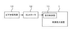
図2は、本発明の実施の形態1に係る映像表示装置1の使用態様を示す構成図である。表示制御部11は、図2に示すように、映像表示装置1に備えられ、回路基板22に配置される電気回路である。表示制御部11は、図示しない電源から個々の発光素子33へ供給される電力を制御して発光素子33の輝度を調整することにより、発光素子33を備える発光装置31の輝度及び発色を調整する。このようにして、表示制御部11は、映像表示装置1に表示される映像の表示制御を行う。  FIG. 2 is a configuration diagram showing how the video display device 1 according to Embodiment 1 of the present invention is used. As shown in FIG. 2, thedisplay control unit 11 is an electric circuit provided in the video display device 1 and disposed on thecircuit board 22. Thedisplay control unit 11 adjusts the luminance and color of thelight emitting device 31 including thelight emitting element 33 by controlling the power supplied to eachlight emitting element 33 from a power source (not shown) to adjust the luminance of thelight emitting element 33. . In this way, thedisplay control unit 11 performs display control of the video displayed on the video display device 1.

映像表示装置1は、図2に示すように、コントローラ12を介してビデオ信号源13に接続される。ビデオ信号源13は、例えば、事前に保存されたビデオ信号をコントローラ12に出力するサーバである。コントローラ12は、ビデオ信号源13から入力されたビデオ信号を、映像表示装置1における発光装置31の配列に合わせて変換し、個々の発光装置31の輝度及び発色を決定し、表示制御部11に出力するコンピュータである。  As shown in FIG. 2, the video display device 1 is connected to avideo signal source 13 via acontroller 12. Thevideo signal source 13 is, for example, a server that outputs a video signal stored in advance to thecontroller 12. Thecontroller 12 converts the video signal input from thevideo signal source 13 in accordance with the arrangement of thelight emitting devices 31 in the video display device 1, determines the luminance and color development of eachlight emitting device 31, and sends it to thedisplay control unit 11. It is a computer that outputs.

このように、映像表示装置1は、マトリクス状に複数配置された映像表示ユニット21の上に、マトリクス状に複数配置された発光装置31の輝度及び発色を個々独立に調整し、画像を表示する。そして、画像を時間の経過に従って変化させ、動画像(映像)を表示する。  As described above, the video display device 1 individually adjusts the luminance and color of thelight emitting devices 31 arranged in a matrix on thevideo display units 21 arranged in a matrix, and displays an image. . Then, the image is changed over time, and a moving image (video) is displayed.

映像表示ユニット21の構成について説明する。
図3(a)は、本発明の実施の形態1に係る映像表示ユニット21の平面図である。図3(b)は、本発明の実施の形態1に係る映像表示ユニット21の側面図である。映像表示ユニット21は、図3に示すように、回路基板22と、回路基板22の上に縦方向及び横方向にマトリクス状に複数配置された発光装置31と、回路基板22の上に形成されて回路基板22を被覆する被覆部材23とを備える。映像表示ユニット21は、図3に示すように、縦方向に4列、横方向に4列、配置された発光装置31を備える。隣接する発光装置31の間隔としては、例えば10mmまたは16mm等が用いられるが、映像表示ユニット21または映像表示装置1に要求される解像度に応じて任意に決定される。
The configuration of thevideo display unit 21 will be described.
FIG. 3A is a plan view of thevideo display unit 21 according to Embodiment 1 of the present invention. FIG. 3B is a side view of thevideo display unit 21 according to Embodiment 1 of the present invention. As shown in FIG. 3, thevideo display unit 21 is formed on thecircuit board 22, a plurality oflight emitting devices 31 arranged in a matrix in the vertical and horizontal directions on thecircuit board 22, and thecircuit board 22. And a coveringmember 23 that covers thecircuit board 22. As shown in FIG. 3, thevideo display unit 21 includeslight emitting devices 31 arranged in four rows in the vertical direction and four rows in the horizontal direction. For example, 10 mm or 16 mm is used as the interval between the adjacentlight emitting devices 31, and is arbitrarily determined according to the resolution required for thevideo display unit 21 or the video display device 1.

回路基板22の表面には、図示しない配線パターンが形成される。発光装置31は、その配線パターンの上に、はんだ付け等で電気的に接続される。電源からの電力は、配線パターンを介して、個々の発光装置31に供給される。  A wiring pattern (not shown) is formed on the surface of thecircuit board 22. Thelight emitting device 31 is electrically connected to the wiring pattern by soldering or the like. The power from the power source is supplied to each light emittingdevice 31 via the wiring pattern.

回路基板22の材料としては、ガラス繊維性の布を重ねたものにエポキシ樹脂を含浸させたガラスエポキシ樹脂が用いられるが、その他の材料を用いてもよい。  As a material of thecircuit board 22, a glass epoxy resin obtained by impregnating an epoxy resin with a glass fiber cloth piled up is used, but other materials may be used.

発光装置31の構成について説明する。
図4(a)は、本発明の実施の形態1に係る発光装置31の平面図である。図4(b)は、本発明の実施の形態1に係る発光装置31の正面図である。図4(c)は、図4(a)に示す発光装置31をB−B線で矢視した断面図である。発光装置31は、図4に示すように、上面に凹部44が形成されたパッケージ32と、パッケージ32の凹部44に配置された発光素子33と、発光素子33の正極と電気的に接続された第1リードフレーム34と、発光素子33の負極と電気的に接続された第2リードフレーム35と、発光素子33の負極と第2リードフレーム35とを電気的に接続するワイヤと、パッケージ32の凹部44に充填されており発光素子33が封止されパッケージ32の上面41より盛り上がって形成された封止部材37とを備える。
The configuration of thelight emitting device 31 will be described.
FIG. 4A is a plan view of thelight emitting device 31 according to Embodiment 1 of the present invention. FIG.4 (b) is a front view of the light-emittingdevice 31 which concerns on Embodiment 1 of this invention. FIG.4 (c) is sectional drawing which looked at the light-emittingdevice 31 shown to Fig.4 (a) at the BB line. As shown in FIG. 4, thelight emitting device 31 is electrically connected to apackage 32 having arecess 44 formed on the upper surface, alight emitting element 33 disposed in therecess 44 of thepackage 32, and a positive electrode of thelight emitting element 33. Afirst lead frame 34; asecond lead frame 35 electrically connected to the negative electrode of thelight emitting element 33; a wire electrically connecting the negative electrode of thelight emitting element 33 and thesecond lead frame 35; And a sealingmember 37 that is filled in therecess 44 and sealed with thelight emitting element 33 and formed so as to rise from theupper surface 41 of thepackage 32.

本発明の実施の形態1では、図4に示すように、いわゆる3in1型の発光装置31を用いる。したがって、発光装置31は、発光素子33として3つの発光素子33r、33g、33bを、第1リードフレーム34として3つの第1リードフレーム34r、34g、34bを、第2リードフレーム35として3つの第2リードフレーム35r、35g、35bを、ワイヤとして3つのワイヤ36r、36g、36bを備える。  In the first embodiment of the present invention, as shown in FIG. 4, a so-called 3 in 1 typelight emitting device 31 is used. Accordingly, thelight emitting device 31 includes three light emittingelements 33r, 33g, and 33b as thelight emitting element 33, threefirst lead frames 34r, 34g, and 34b as thefirst lead frame 34, and three first lead frames 35 as thesecond lead frame 35. The twolead frames 35r, 35g, and 35b are provided with threewires 36r, 36g, and 36b as wires.

パッケージ32の形状は直方体である。図4に示すように、パッケージ32には、上面41に凹部44が形成される。凹部44は、逆円錐台の形状であって、上面41からパッケージ32の内側に形成された窪みである。凹部44は、パッケージ32の側面45及び底面46を逆円錐台の形状の外周としている。  The shape of thepackage 32 is a rectangular parallelepiped. As shown in FIG. 4, arecess 44 is formed on theupper surface 41 of thepackage 32. Therecess 44 has a shape of an inverted truncated cone, and is a recess formed from theupper surface 41 to the inside of thepackage 32. Therecess 44 has aside surface 45 and abottom surface 46 of thepackage 32 as an outer periphery in the shape of an inverted truncated cone.

パッケージ32の凹部44には、図4に示すように、発光素子33r、33g、33b、第1リードフレーム34r、34g、34b、第2リードフレーム35r、35g、35b、及びワイヤ36r、36g、36bが配置される。発光素子33r、33g、33bは、縦方向に一列に並ぶ。  4, thelight emitting elements 33r, 33g, 33b, thefirst lead frames 34r, 34g, 34b, thesecond lead frames 35r, 35g, 35b, and thewires 36r, 36g, 36b Is placed. Thelight emitting elements 33r, 33g, and 33b are arranged in a line in the vertical direction.

発光素子33rは赤色の光を発光し、発光素子33gは緑色の光を発光し、発光素子33bは青色の光を発光する。発光素子33r、33g、33bは、個々独立に任意の電力が供給され、個々独立に任意の輝度の光を発光する。したがって、発光装置31としては、任意の輝度及び発色を実現することができる。  Thelight emitting element 33r emits red light, thelight emitting element 33g emits green light, and thelight emitting element 33b emits blue light. Thelight emitting elements 33r, 33g, and 33b are supplied with arbitrary electric power independently and emit light of arbitrary luminance independently. Therefore, thelight emitting device 31 can realize arbitrary luminance and color development.

発光素子33としては、発光ダイオードまたは半導体レーザのような化合物半導体素子が用いられる。化合物半導体素子は、構成するインジウム(In)、アルミニウム(Al)、またはガリウム(Ga)等の組成を調整することにより、発光する光の波長を、赤、緑、青、等の任意の波長に調整することができる。  As thelight emitting element 33, a compound semiconductor element such as a light emitting diode or a semiconductor laser is used. The compound semiconductor element adjusts the composition of indium (In), aluminum (Al), gallium (Ga), etc., to adjust the wavelength of emitted light to an arbitrary wavelength such as red, green, blue, etc. Can be adjusted.

発光素子33rは、図4に示すように、パッケージ32の凹部44の底面46に配置された第1リードフレーム34rの上に、配置される。発光素子33rの正極は、第1リードフレーム34rと電気的に接続される。発光素子33rの負極は、ワイヤ36rを介して、パッケージ32の凹部44の底面46に配置された第2リードフレーム35rと、電気的に接続される。  As shown in FIG. 4, thelight emitting element 33 r is disposed on thefirst lead frame 34 r disposed on thebottom surface 46 of therecess 44 of thepackage 32. The positive electrode of thelight emitting element 33r is electrically connected to thefirst lead frame 34r. The negative electrode of thelight emitting element 33r is electrically connected to thesecond lead frame 35r disposed on thebottom surface 46 of therecess 44 of thepackage 32 through thewire 36r.

発光素子33gは、図4に示すように、パッケージ32の凹部44の底面46に配置された第1リードフレーム34gの上に、配置される。発光素子33gの正極は、第1リードフレーム34gと電気的に接続される。発光素子33gの負極は、ワイヤ36gを介して、パッケージ32の凹部44の底面46に配置された第2リードフレーム35gと、電気的に接続される。  As illustrated in FIG. 4, thelight emitting element 33 g is disposed on thefirst lead frame 34 g disposed on thebottom surface 46 of therecess 44 of thepackage 32. The positive electrode of thelight emitting element 33g is electrically connected to thefirst lead frame 34g. The negative electrode of thelight emitting element 33g is electrically connected to thesecond lead frame 35g disposed on thebottom surface 46 of therecess 44 of thepackage 32 via thewire 36g.

発光素子33bは、図4に示すように、パッケージ32の凹部44の底面46に配置された第1リードフレーム34bの上に、配置される。発光素子33bの正極は、第1リードフレーム34bと電気的に接続される。発光素子33bの負極は、ワイヤ36bを介して、パッケージ32の凹部44の底面46に配置された第2リードフレーム35bと、電気的に接続される。  As shown in FIG. 4, thelight emitting element 33 b is disposed on thefirst lead frame 34 b disposed on thebottom surface 46 of therecess 44 of thepackage 32. The positive electrode of thelight emitting element 33b is electrically connected to thefirst lead frame 34b. The negative electrode of thelight emitting element 33b is electrically connected to thesecond lead frame 35b disposed on thebottom surface 46 of therecess 44 of thepackage 32 through thewire 36b.

第1リードフレーム34r、34g、34b、及び第2リードフレーム35r、35g、35bの材料としては、金、銅等の金属が用いられる。第1リードフレーム34r、34g、34b、及び第2リードフレーム35r、35g、35bは、電源からの電力を発光素子33へ供給する。  As materials for thefirst lead frames 34r, 34g, 34b and thesecond lead frames 35r, 35g, 35b, metals such as gold and copper are used. Thefirst lead frames 34r, 34g, 34b and thesecond lead frames 35r, 35g, 35b supply power from the power source to thelight emitting element 33.

第1リードフレーム34gの形状は、板状である。第1リードフレーム34gは、図4(c)に示すように、一端がパッケージ32の凹部44の底面46に位置し、パッケージ32の凹部44の底面46に沿ってパッケージ32の凹部44の左側の側面45に向かって延び、パッケージ32の凹部44の左側の側面45からパッケージ32の内部を通過してパッケージ32の底面43に突出し、パッケージ32の底面43に沿ってパッケージ32の左側の側面42の方向に向かって延び、パッケージ32の左側の側面42の下方から突出する。  Thefirst lead frame 34g has a plate shape. As shown in FIG. 4C, one end of thefirst lead frame 34g is located on thebottom surface 46 of therecess 44 of thepackage 32, and thefirst lead frame 34g is located on the left side of therecess 44 of thepackage 32 along thebottom surface 46 of therecess 44 of thepackage 32. It extends toward theside surface 45, passes through the inside of thepackage 32 from theleft side surface 45 of therecess 44 of thepackage 32, protrudes to thebottom surface 43 of thepackage 32, and extends along thebottom surface 43 of thepackage 32 to theleft side surface 42 of thepackage 32. It extends in the direction and projects from below theleft side surface 42 of thepackage 32.

第1リードフレーム34r、34bも、上述の第1リードフレーム34gと同様の形状、構造及び機能有する。  The first lead frames 34r and 34b also have the same shape, structure and function as thefirst lead frame 34g described above.

第2リードフレーム35gの形状は、板状である。第2リードフレーム35gは、図4(c)に示すように、一端がパッケージ32の凹部44の底面46に位置し、パッケージ32の凹部44の底面46に沿ってパッケージ32の凹部44の右側の側面45に向かって延び、パッケージ32の凹部44の右側の側面45からパッケージ32の内部を通過してパッケージ32の底面43に突出し、パッケージ32の底面43に沿ってパッケージ32の右側の側面42の方向に向かって延び、パッケージ32の右側の側面42の下方から突出する。  Thesecond lead frame 35g has a plate shape. 4C, one end of thesecond lead frame 35g is positioned on thebottom surface 46 of theconcave portion 44 of thepackage 32, and the right side of theconcave portion 44 of thepackage 32 along thebottom surface 46 of theconcave portion 44 of thepackage 32. It extends toward theside surface 45, passes through the inside of thepackage 32 from theright side surface 45 of therecess 44 of thepackage 32, protrudes to thebottom surface 43 of thepackage 32, and extends along thebottom surface 43 of thepackage 32 to theright side surface 42 of thepackage 32. It extends in the direction and protrudes from below theright side surface 42 of thepackage 32.

第2リードフレーム35r、35bも、上述の第2リードフレーム35gと同様の形状、構造及び効果を有する。  The second lead frames 35r and 35b also have the same shape, structure and effect as the above-described secondlead frame 35g.

このように、第1リードフレーム34r、34g、34b、及び第2リードフレーム35r、35g、35bは、一部がパッケージ32に埋め込まれるように、配置される。したがって、第1リードフレーム34r、34g、34b、及び第2リードフレーム35r、35g、35bは、パッケージ32にしっかりと固定されるため、映像表示装置1が震動する環境に設置された場合でも、電気的な断線から免れることができる。  As described above, the first lead frames 34 r, 34 g, 34 b and the second lead frames 35 r, 35 g, 35 b are arranged so as to be partially embedded in thepackage 32. Accordingly, thefirst lead frames 34r, 34g, 34b and thesecond lead frames 35r, 35g, 35b are firmly fixed to thepackage 32, so that even when the video display device 1 is installed in an environment that vibrates, the electric Can be freed from a severe disconnection.

第1リードフレーム34r、34g、34b、及び第2リードフレーム35r、35g、35bのサイズは、パッケージ32のサイズ等に応じて任意に選択される。  The sizes of thefirst lead frames 34r, 34g, 34b and thesecond lead frames 35r, 35g, 35b are arbitrarily selected according to the size of thepackage 32 and the like.

ワイヤ36r、36g、36bは、発光素子33r、33g、33bと、第2リードフレーム35r、35g、35bとを、それぞれ電気的に接続する導電性の配線である。ワイヤ36r、36g、36bの材料としては、金、銅等の金属が用いられる。  Thewires 36r, 36g, and 36b are conductive wirings that electrically connect thelight emitting elements 33r, 33g, and 33b and thesecond lead frames 35r, 35g, and 35b, respectively. As a material of thewires 36r, 36g, and 36b, a metal such as gold or copper is used.

パッケージ32の凹部44に配置された、発光素子33r、33g、33b、第1リードフレーム34r、34g、34bの一部、第2リードフレーム35r、35g、35bの一部、及びワイヤ36r、36g、36bは、パッケージ32の凹部44に充填された封止部材37により、封止される。これにより、発光素子33r、33g、33b、第1リードフレーム34r、34g、34bの一部、第2リードフレーム35r、35g、35bの一部、及びワイヤ36r、36g、36bを、水分、塵芥、外力等から保護することができる。  Thelight emitting elements 33r, 33g, 33b, a part of thefirst lead frames 34r, 34g, 34b, a part of thesecond lead frames 35r, 35g, 35b, and thewires 36r, 36g, arranged in therecess 44 of thepackage 32, 36 b is sealed by a sealingmember 37 filled in therecess 44 of thepackage 32. Thus, thelight emitting elements 33r, 33g, 33b, a part of thefirst lead frames 34r, 34g, 34b, a part of thesecond lead frames 35r, 35g, 35b, and thewires 36r, 36g, 36b It can be protected from external forces.

パッケージ32のサイズは、映像表示ユニット21に要求される画素サイズ等に応じて任意に選択される。パッケージ32の材料としては、エポキシ樹脂等の樹脂が用いられる。なお、パッケージ32に用いられる樹脂は、発光素子33r、33g、33bが発光する光を吸収する樹脂が用いられる。これにより、隣接する画素の混色を防止することができる。  The size of thepackage 32 is arbitrarily selected according to the pixel size required for thevideo display unit 21. As a material of thepackage 32, a resin such as an epoxy resin is used. The resin used for thepackage 32 is a resin that absorbs light emitted from thelight emitting elements 33r, 33g, and 33b. Thereby, color mixing of adjacent pixels can be prevented.

封止部材37としては、シリコン樹脂等の樹脂が用いられる。なお、封止部材37に用いられる樹脂は、発光素子33r、33g、33bが発光する光を透過する樹脂、つまり発光素子33r、33g、33bが発光する光に対して透明な樹脂が用いられる。これにより、発光素子33r、33g、33bが発光した光が、発光装置31の外部に出射することができ、映像表示装置1を見る人物が映像を知覚することができる。  As the sealingmember 37, a resin such as a silicone resin is used. The resin used for the sealingmember 37 is a resin that transmits light emitted from thelight emitting elements 33r, 33g, and 33b, that is, a resin that is transparent to light emitted from thelight emitting elements 33r, 33g, and 33b. Thereby, the light emitted by thelight emitting elements 33r, 33g, and 33b can be emitted to the outside of thelight emitting device 31, and the person who views the video display device 1 can perceive the video.

封止部材37は、次のようにして、パッケージ32の凹部44に充填される。先ず、封止部材37が、液体の状態で、パッケージ32の凹部44に注入される。パッケージ32の凹部44は、液体状態の封止部材37で、充填される。このとき、パッケージ32の凹部44の容積を超える量の封止部材37が注入されると、余分な封止部材37が、表面張力の作用で、パッケージ32の上面41より凸レンズの一部形状をなして盛り上がる。この状態で封止部材37が硬化すると、パッケージ32の凹部44を充填し、さらにパッケージ32の上面41より凸レンズの一部形状をなして盛り上がった封止部材37が、形成される。ここで、パッケージ32の上面41より盛り上がる凸レンズの一部形状とは、平凸レンズの形状に相当する。  The sealingmember 37 is filled in therecess 44 of thepackage 32 as follows. First, the sealingmember 37 is injected into therecess 44 of thepackage 32 in a liquid state. Therecess 44 of thepackage 32 is filled with a sealingmember 37 in a liquid state. At this time, when an amount of the sealingmember 37 exceeding the volume of theconcave portion 44 of thepackage 32 is injected, theextra sealing member 37 causes a partial shape of the convex lens from theupper surface 41 of thepackage 32 due to the action of surface tension. It ’s exciting. When the sealingmember 37 is cured in this state, the sealingmember 37 that fills theconcave portion 44 of thepackage 32 and further rises from theupper surface 41 of thepackage 32 to form a part of the convex lens is formed. Here, the partial shape of the convex lens raised from theupper surface 41 of thepackage 32 corresponds to the shape of a plano-convex lens.

図5は、本発明の実施の形態1に係る映像表示ユニット21を図3(a)に示すA−A線に相当する位置から矢視した断面の一部を示す図である。封止部材37がパッケージ32の凹部44を充填するため、パッケージ32と封止部材37との間には、パッケージ32の凹部44の側面45及び底面46からなる境界面が形成される。ここで、図3及び図5に示すように、パッケージ32と封止部材37との境界面の外縁部51を、被覆部材で被覆されていない場合にパッケージ32と封止部材37との境界面が外部の空間と接触する部分と定義する。つまり、パッケージ32と封止部材37との境界面の外縁部51は、パッケージ32の上面41より凸レンズの一部形状をなして盛り上がった封止部材37を取り囲む周縁部でもある。  FIG. 5 is a view showing a part of a cross section of thevideo display unit 21 according to Embodiment 1 of the present invention as viewed from the position corresponding to the line AA shown in FIG. Since the sealingmember 37 fills therecess 44 of thepackage 32, a boundary surface including aside surface 45 and abottom surface 46 of therecess 44 of thepackage 32 is formed between thepackage 32 and the sealingmember 37. Here, as shown in FIGS. 3 and 5, when theouter edge portion 51 of the boundary surface between thepackage 32 and the sealingmember 37 is not covered with the covering member, the boundary surface between thepackage 32 and the sealingmember 37. Is defined as the part in contact with the external space. That is, theouter edge portion 51 at the boundary surface between thepackage 32 and the sealingmember 37 is also a peripheral portion surrounding the sealingmember 37 that is raised from theupper surface 41 of thepackage 32 to form a partial shape of a convex lens.

図6は、図4(c)に示す発光装置31の断面図で、凸レンズの作用を説明する図である。パッケージ32の上面41より凸レンズの一部形状をなして盛り上がった封止部材37が示す、凸レンズの作用について、図6を参照して、説明する。封止部材37が凸レンズの一部形状をなして盛り上がっていないと仮定すると、つまり封止部材37が水平面であると仮定すると、発光素子33が発光した光は封止部材37の周縁部に入射角iで入射し、屈折角rで出射する。しかし、実際には、封止部材37は凸レンズの一部形状をなして盛り上がっているため、発光素子33gが発光した光は封止部材37の周縁部に入射角iで入射し、屈折角rで出射する。入射角iは入射角iより小さいため、屈折角rは屈折角rよりも小さくなる。したがって、封止部材37が凸レンズの一部形状をなして盛り上がっている場合には、発光装置31を出射した光の方向は光軸61に近くなり、集光特性が向上し、映像表示ユニット21は鮮明な映像を表示することができる。FIG. 6 is a cross-sectional view of thelight emitting device 31 shown in FIG. The operation of the convex lens shown by the sealingmember 37 raised from theupper surface 41 of thepackage 32 in the shape of a part of the convex lens will be described with reference to FIG. Assuming that the sealingmember 37 does not rise as a part of the convex lens, that is, if the sealingmember 37 is assumed to be a horizontal plane, the light emitted from thelight emitting element 33 enters the peripheral portion of the sealingmember 37. It enters at an angle i0 and exits at a refraction angle r0 . However, in practice, the sealingmember 37 because it has raised forms part of a convex lens shape, thelight emitting element 33g emits light is incident at an incident angle i1 to the peripheral portion of the sealingmember 37, the angle of refraction emitted at r1. Since the incident angle i1 is smaller than the incident angle i0 , the refraction angle r1 is smaller than the refraction angle r0 . Therefore, when the sealingmember 37 is raised by forming a partial shape of a convex lens, the direction of the light emitted from thelight emitting device 31 is close to theoptical axis 61, the light collection characteristic is improved, and thevideo display unit 21. Can display clear video.

ところで、封止部材37は液体の状態でパッケージ32の凹部44に注入されるため、パッケージ32の凹部44に封止部材37を隙間なく充填することができる。しかし、長期間に亘る使用の中で、パッケージ32及び封止部材37は膨張と収縮を繰り返し、封止部材37がパッケージ32の凹部44の側面45から剥離してしまう場合がある。何ら対策がない場合は、パッケージ32の凹部44の側面45と封止部材37との間に生じた隙間から水が浸入し、発光素子33r、33g、33b、第1リードフレーム34r、34g、34b、第2リードフレーム35r、35g、35b、またはワイヤ36r、36g、36bが腐食し、映像表示装置1に表示される映像の劣化の原因となる。  By the way, since the sealingmember 37 is injected into therecess 44 of thepackage 32 in a liquid state, the sealingmember 37 can be filled in therecess 44 of thepackage 32 without a gap. However, thepackage 32 and the sealingmember 37 repeatedly expand and contract during use over a long period of time, and the sealingmember 37 may peel from theside surface 45 of therecess 44 of thepackage 32 in some cases. If no countermeasures are taken, water enters from the gap formed between theside surface 45 of therecess 44 of thepackage 32 and the sealingmember 37, and thelight emitting elements 33r, 33g, 33b, thefirst lead frames 34r, 34g, 34b. Thesecond lead frames 35r, 35g, and 35b or thewires 36r, 36g, and 36b are corroded to cause deterioration of an image displayed on the image display device 1.

そこで、本発明では、図3及び図5で示すように、パッケージ32と封止部材37との境界面の外縁部51を、被覆部材23で被覆する構造を採用する。  Therefore, in the present invention, as shown in FIGS. 3 and 5, a structure in which theouter edge portion 51 of the boundary surface between thepackage 32 and the sealingmember 37 is covered with the coveringmember 23 is employed.

被覆部材23は、次のようにして、回路基板22の上に形成されて、回路基板22を被覆する。被覆部材23は、液体の状態で、回路基板22の上に縦方向及び横方向にマトリクス状に配列した個々の発光装置31の間に、注入される。注入された被覆部材23は、先ず回路基板22の上で徐々に広がり、回路基板22を被覆する。さらに被覆部材23が注入されると、被覆部材23の液面は徐々に上昇していく。被覆部材23が、パッケージ32と封止部材37との境界面の外縁部51を被覆した時に、被覆部材23の注入は停止される。このとき、発光装置31の周囲の被覆部材23の液面は、図5に示すように、表面張力の作用により、発光装置31に近づくにつれて、次第に盛り上がり、高くなる。この状態で被覆部材23が硬化すると、被覆部材23が、回路基板22、パッケージ32の側面42の下方から突出した第1リードフレーム34r、34g、34b、及び第2リードフレーム35r、35g、35b、パッケージ32の側面42、並びにパッケージ32と封止部材37との境界面の外縁部51を被覆し、かつ、発光装置31に近づくにつれて、被覆部材23が次第に盛り上がり高くなる構造が形成される。  The coveringmember 23 is formed on thecircuit board 22 as follows to cover thecircuit board 22. The coveringmember 23 is injected between the individuallight emitting devices 31 arranged in a matrix in the vertical and horizontal directions on thecircuit board 22 in a liquid state. The coated coveringmember 23 is first spread gradually on thecircuit board 22 to cover thecircuit board 22. When the coveringmember 23 is further injected, the liquid level of the coveringmember 23 gradually increases. When the coveringmember 23 covers theouter edge portion 51 of the boundary surface between thepackage 32 and the sealingmember 37, the injection of the coveringmember 23 is stopped. At this time, as shown in FIG. 5, the liquid level of the coveringmember 23 around thelight emitting device 31 gradually rises and becomes higher as it approaches thelight emitting device 31 due to the action of surface tension. When the coveringmember 23 is cured in this state, the coveringmember 23 is protruded from below thecircuit board 22, theside surface 42 of thepackage 32, and thefirst lead frames 34r, 34g, 34b, and thesecond lead frames 35r, 35g, 35b, A structure is formed in which theside surface 42 of thepackage 32 and theouter edge portion 51 of the boundary surface between thepackage 32 and the sealingmember 37 are covered and the coveringmember 23 gradually rises as thelight emitting device 31 is approached.

このようにして形成された被覆部材23は、回路基板22、並びにパッケージ32の側面42の下方から突出した第1リードフレーム34r、34g、34b、及び第2リードフレーム35r、35g、35bを被覆するため、回路基板22の上に形成された配線パターン、並びにパッケージ32の側面42の下方から突出した第1リードフレーム34r、34g、34b、及び第2リードフレーム35r、35g、35bを、水分による腐食から保護することができる。  The coveringmember 23 thus formed covers thecircuit board 22 and thefirst lead frames 34r, 34g, 34b and thesecond lead frames 35r, 35g, 35b protruding from below theside surface 42 of thepackage 32. Therefore, the wiring pattern formed on thecircuit board 22 and thefirst lead frames 34r, 34g, 34b and thesecond lead frames 35r, 35g, 35b protruding from below theside surface 42 of thepackage 32 are corroded by moisture. Can be protected from.

また、被覆部材23は、パッケージ32と封止部材37との境界面の外縁部51を被覆するため、長期間の使用の中で封止部材37がパッケージ32の凹部44の側面45から剥離してしまった場合でも、パッケージ32の凹部44の側面45と封止部材37との間に生じた隙間への水の浸入を防止し、発光素子33r、33g、33b、第1リードフレーム34r、34g、34b、第2リードフレーム35r、35g、35b、またはワイヤ36r、36g、36bを、水分による腐食から保護することができる。  Further, since the coveringmember 23 covers theouter edge portion 51 of the boundary surface between thepackage 32 and the sealingmember 37, the sealingmember 37 peels from theside surface 45 of therecess 44 of thepackage 32 during long-term use. Even if it has, the intrusion of water into the gap formed between theside surface 45 of therecess 44 of thepackage 32 and the sealingmember 37 is prevented, and thelight emitting elements 33r, 33g, 33b, thefirst lead frames 34r, 34g , 34b, thesecond lead frames 35r, 35g, 35b or thewires 36r, 36g, 36b can be protected from corrosion due to moisture.

さらに、被覆部材23は、図3及び図5に示すように、パッケージ32と封止部材37との境界面の外縁部51を被覆し、さらにパッケージ32の上面41より凸レンズの一部形状をなして盛り上がった封止部材37の周辺部も被覆する。このため、長期間の使用の中で封止部材37がパッケージ32の凹部44の側面45から剥離し、パッケージ32の凹部44の側面45と封止部材37との間に隙間が生じた場合でも、隙間への水の浸入を確実に防止することができる。  Further, as shown in FIGS. 3 and 5, the coveringmember 23 covers theouter edge portion 51 of the boundary surface between thepackage 32 and the sealingmember 37, and further forms a part of the convex lens from theupper surface 41 of thepackage 32. The peripheral part of the sealingmember 37 raised is also covered. For this reason, even when the sealingmember 37 peels from theside surface 45 of therecess 44 of thepackage 32 during a long period of use, and a gap is generated between theside surface 45 of therecess 44 of thepackage 32 and the sealingmember 37. Intrusion of water into the gap can be reliably prevented.

被覆部材23としては、シリコン樹脂等の樹脂が用いられる。なお、被覆部材23に用いられる樹脂は、太陽光等の可視光を吸収する樹脂、つまり可視光に対して不透明な樹脂である。被覆部材23が可視光を吸収するため、回路基板22の表面における太陽光等の外光の反射を抑制することができ、映像表示ユニット21に表示される映像のコントラストを向上することができる。  As the coveringmember 23, a resin such as silicon resin is used. The resin used for the coveringmember 23 is a resin that absorbs visible light such as sunlight, that is, a resin that is opaque to visible light. Since the coveringmember 23 absorbs visible light, reflection of external light such as sunlight on the surface of thecircuit board 22 can be suppressed, and the contrast of an image displayed on theimage display unit 21 can be improved.

以上のように、本発明の実施の形態1では、被覆部材23が発光装置31のパッケージ32と封止部との境界面の外縁部を被覆するため、従来よりも防水性能に優れた映像表示ユニット21、及びその映像表示ユニット21を備える映像表示装置1を提供することができる。  As described above, in the first embodiment of the present invention, since the coveringmember 23 covers the outer edge portion of the boundary surface between thepackage 32 and the sealing portion of thelight emitting device 31, an image display that is superior in waterproof performance than before. Theunit 21 and the video display device 1 including thevideo display unit 21 can be provided.

実施の形態2.
本発明の実施の形態2に係る映像表示ユニット21及び映像表示装置1について添付の図面を参照しながら説明する。なお、実施の形態2に係る映像表示ユニット21及び映像表示装置1の説明において、実施の形態1に係る映像表示ユニット21及び映像表示装置1の構成と共通する構成要素には共通の符号を用い、その説明の一部または全部を適宜省略する場合がある。
Embodiment 2. FIG.
Avideo display unit 21 and a video display device 1 according toEmbodiment 2 of the present invention will be described with reference to the accompanying drawings. In the description of thevideo display unit 21 and the video display device 1 according to the second embodiment, common reference numerals are used for components that are common to the configurations of thevideo display unit 21 and the video display device 1 according to the first embodiment. Some or all of the description may be omitted as appropriate.

図7は、本発明の実施の形態2に係る映像表示ユニット21を、図3(a)に示すA−A線に相当する位置から矢視した断面の一部を示す図である。映像表示ユニット21は、図7に示すように、回路基板22と、回路基板22の上に縦方向及び横方向にマトリクス状に複数配置された発光装置31と、回路基板22の上に形成されて回路基板22を被覆する第1被覆部材24と、回路基板22の上に形成されてパッケージ32の側面42及びパッケージ32と封止部材37との境界面の外縁部51を被覆する第2被覆部材25とを備える。  FIG. 7 is a view showing a part of a cross section of thevideo display unit 21 according to the second embodiment of the present invention as viewed from the position corresponding to the line AA shown in FIG. As shown in FIG. 7, thevideo display unit 21 is formed on thecircuit board 22, a plurality of light emittingdevices 31 arranged in a matrix in the vertical and horizontal directions on thecircuit board 22, and thecircuit board 22. Afirst covering member 24 that covers thecircuit board 22 and a second covering that is formed on thecircuit board 22 and covers theside surface 42 of thepackage 32 and theouter edge 51 of the boundary surface between thepackage 32 and the sealingmember 37. And amember 25.

第1被覆部材24及び第2被覆部材25は、次のようにして、回路基板22の上に形成する。先ず、実施の形態1と同様に、第2被覆部材25が、液体の状態で、回路基板22の上に縦方向及び横方向にマトリクス状に配列した個々の発光装置31の間に、注入される。注入された第2被覆部材25は、先ず回路基板22の上に徐々に広がり、回路基板22の上を被覆する。さらに第2被覆部材25が注入されると、第2被覆部材25の液面は徐々に上昇していく。第2被覆部材25が、パッケージ32と封止部材37との境界面の外縁部51を被覆した時に、第2被覆部材25の注入が停止される。このとき、発光装置31の周囲の第2被覆部材25の液面は、表面張力の作用により、発光装置31に近づくにつれて、次第に盛り上がり、高くなる。この状態で第2被覆部材25が硬化すると、第2被覆部材25が、回路基板22、パッケージ32の側面42の下方から突出した第1リードフレーム34r、34g、34b、及び第2リードフレーム35r、35g、35b、パッケージ32の側面42、並びにパッケージ32と封止部材37との境界面の外縁部51を被覆し、かつ、発光装置31に近づくにつれて、第2被覆部材25が次第に盛り上がり高くなる構造が形成される。  Thefirst covering member 24 and thesecond covering member 25 are formed on thecircuit board 22 as follows. First, as in the first embodiment, thesecond covering member 25 is injected between the individuallight emitting devices 31 arranged in a matrix in the vertical and horizontal directions on thecircuit board 22 in a liquid state. The The injected second coveringmember 25 first gradually spreads over thecircuit board 22 and covers thecircuit board 22. When thesecond covering member 25 is further injected, the liquid level of thesecond covering member 25 gradually rises. When thesecond covering member 25 covers theouter edge portion 51 of the boundary surface between thepackage 32 and the sealingmember 37, the injection of thesecond covering member 25 is stopped. At this time, the liquid level of thesecond covering member 25 around thelight emitting device 31 gradually rises and becomes higher as it approaches thelight emitting device 31 due to the action of surface tension. When thesecond covering member 25 is cured in this state, thesecond covering member 25 is provided with thefirst lead frames 34r, 34g, 34b, and thesecond lead frame 35r protruding from below theside surface 42 of thecircuit board 22, thepackage 32, and thesecond lead frame 35r. 35g, 35b, theside surface 42 of thepackage 32, and theouter edge portion 51 of the boundary surface between thepackage 32 and the sealingmember 37, and thesecond covering member 25 gradually rises and becomes higher as thelight emitting device 31 is approached. Is formed.

次に、回路基板22の上に縦方向及び横方向にマトリクス状に配置した個々の発光装置31の周囲が、図示しないマスク部材により、マスクされる。マスク部材でマスクされていない部分の第2被覆部材25が、エッチングにより、回路基板22の上から除去される。マスク部材が、取り除かれる。  Next, the periphery of each light emittingdevice 31 arranged in a matrix in the vertical direction and the horizontal direction on thecircuit board 22 is masked by a mask member (not shown). The portion of thesecond covering member 25 that is not masked by the mask member is removed from above thecircuit board 22 by etching. The mask member is removed.

次に、第1被覆部材24が、液体の状態で、第2被覆部材25が除去された部分に注入される。注入された第1被覆部材24は、第2被覆部材25が除去された部分の回路基板22の上で徐々に広がり、回路基板22の上を被覆する。さらに第1被覆部材24が注入されると、第1被覆部材24の液面は徐々に上昇していく。第1被覆部材24と第2被覆部材25との接続部において、第1被覆部材24の液面の高さH1が、除去されずに残っている第2被覆部材25の高さH2に達する前に、第1被覆部材24の注入が停止される。この状態で第1被覆部材24が硬化すると、第1被覆部材24と第2被覆部材25との接続部において、回路基板22からの第1被覆部材24の高さH1が、回路基板22からの第2被覆部材25の高さH2よりも低い構造が形成される。  Next, the1st coating member 24 is inject | poured into the part from which the2nd coating member 25 was removed in the liquid state. The injected first coveringmember 24 gradually spreads on the portion of thecircuit board 22 where thesecond covering member 25 is removed, and covers thecircuit board 22. Further, when thefirst covering member 24 is injected, the liquid level of thefirst covering member 24 gradually rises. Before the height H1 of the liquid level of thefirst covering member 24 reaches the height H2 of thesecond covering member 25 remaining without being removed at the connection portion between thefirst covering member 24 and thesecond covering member 25. In addition, the injection of thefirst covering member 24 is stopped. When thefirst covering member 24 is cured in this state, the height H1 of thefirst covering member 24 from thecircuit board 22 at the connecting portion between thefirst covering member 24 and thesecond covering member 25 is from thecircuit board 22. A structure lower than the height H2 of thesecond covering member 25 is formed.

このようにして形成された第1被覆部材24は、回路基板22を被覆するため、回路基板22の上に形成された配線パターンを、水分による腐食から保護することができる。  Since thefirst covering member 24 formed in this manner covers thecircuit board 22, the wiring pattern formed on thecircuit board 22 can be protected from corrosion due to moisture.

また、第2被覆部材25は、パッケージ32の側面42の下方から突出した第1リードフレーム34r、34g、34b、及び第2リードフレーム35r、35g、35bを被覆するため、パッケージ32の側面42の下方から突出した第1リードフレーム34r、34g、34b、及び第2リードフレーム35r、35g、35bを、水分による腐食から保護することができる。  Further, thesecond covering member 25 covers thefirst lead frames 34r, 34g, 34b and thesecond lead frames 35r, 35g, 35b protruding from below theside surface 42 of thepackage 32. Thefirst lead frames 34r, 34g, and 34b and thesecond lead frames 35r, 35g, and 35b protruding from below can be protected from corrosion due to moisture.

また、第2被覆部材25は、パッケージ32と封止部材37との境界面の外縁部51を被覆するため、長期間の使用の中でパッケージ32の凹部44の側面45から封止部材37が剥離してしまった場合でも、パッケージ32の凹部44の側面45と封止部材37との間に生じた隙間への水の浸入を防止し、発光素子33r、33g、33b、第1リードフレーム34r、34g、34b、第2リードフレーム35r、35g、35b、またはワイヤ36r、36g、36bを、水分による腐食から保護することができる。  Further, since thesecond covering member 25 covers theouter edge portion 51 of the boundary surface between thepackage 32 and the sealingmember 37, the sealingmember 37 is removed from theside surface 45 of theconcave portion 44 of thepackage 32 during long-term use. Even if it is peeled off, water can be prevented from entering the gap formed between theside surface 45 of therecess 44 of thepackage 32 and the sealingmember 37, and thelight emitting elements 33r, 33g, 33b, and thefirst lead frame 34r. , 34g, 34b, thesecond lead frames 35r, 35g, 35b, or thewires 36r, 36g, 36b can be protected from moisture corrosion.

さらに、第2被覆部材25は、図3及び図7に示すように、パッケージ32と封止部材37との境界面の外縁部51を被覆し、さらにパッケージ32の上面41より凸レンズの一部形状をなして盛り上がった封止部材37の周辺部も被覆する。このため、長期間の使用の中で封止部材37がパッケージ32の凹部44の側面45から剥離し、パッケージ32の凹部44の側面45と封止部材37との間に隙間が生じた場合でも、隙間への水の浸入を確実に防止することができる。  Further, as shown in FIGS. 3 and 7, thesecond covering member 25 covers theouter edge portion 51 of the boundary surface between thepackage 32 and the sealingmember 37, and further, a partial shape of the convex lens from theupper surface 41 of thepackage 32. The peripheral portion of the sealingmember 37 that rises up is also covered. For this reason, even when the sealingmember 37 peels from theside surface 45 of therecess 44 of thepackage 32 during a long period of use, and a gap is generated between theside surface 45 of therecess 44 of thepackage 32 and the sealingmember 37. Intrusion of water into the gap can be reliably prevented.

第1覆部材としては、シリコン樹脂等の樹脂が用いられる。第1被覆部材24に用いられる樹脂は、太陽光等の可視光を吸収する樹脂、つまり可視光に対して不透明な樹脂である。これにより、回路基板22の表面における太陽光等の外光の反射を抑制することができ、映像表示ユニット21に表示される映像のコントラストを向上することができる。  As the first covering member, a resin such as silicon resin is used. The resin used for thefirst covering member 24 is a resin that absorbs visible light such as sunlight, that is, a resin that is opaque to visible light. Thereby, reflection of external light such as sunlight on the surface of thecircuit board 22 can be suppressed, and the contrast of an image displayed on theimage display unit 21 can be improved.

第2覆部材としては、シリコン樹脂等の樹脂が用いられる。第2被覆部材25に用いられる樹脂は、発光素子33r、33g、33bが発光する光を透過する樹脂、つまり発光素子33r、33g、33bが発光する光に対して透明な樹脂である。これにより、第2被覆部材25が、パッケージ32の上面41より凸レンズの一部形状をなして盛り上がった封止部材37の周辺部を被覆しても、発光素子33r、33g、33bが発光する光が効率よく映像表示ユニット21の外部に出射することができるため、映像表示ユニット21の消費電力を低減することができる。  As the second covering member, a resin such as a silicon resin is used. The resin used for thesecond covering member 25 is a resin that transmits light emitted from thelight emitting elements 33r, 33g, and 33b, that is, a resin that is transparent to light emitted from thelight emitting elements 33r, 33g, and 33b. As a result, even if thesecond covering member 25 covers the peripheral portion of the sealingmember 37 that forms a part of the convex lens from theupper surface 41 of thepackage 32, the light emitted from thelight emitting elements 33r, 33g, and 33b. Can be efficiently emitted to the outside of thevideo display unit 21, so that the power consumption of thevideo display unit 21 can be reduced.

第1被覆部材24は、液面の高さH1が、除去されずに残っている第2被覆部材25の高さH2に達する前に、注入が停止される。したがって、可視光を吸収する第1被覆部材24の注入量過多により、第1被覆部材24が発光装置31を被覆してしまい、発光装置31が発色できないという事態を防止することができる。また、第1被覆部材24の注入量が少なくて済むため、第1被覆部材24のコストを低減することができる。  Injection of thefirst covering member 24 is stopped before the liquid surface height H1 reaches the height H2 of thesecond covering member 25 remaining without being removed. Therefore, it is possible to prevent a situation in which thefirst covering member 24 covers thelight emitting device 31 due to an excessive injection amount of thefirst covering member 24 that absorbs visible light, and thelight emitting device 31 cannot develop color. Further, since the injection amount of thefirst covering member 24 can be small, the cost of thefirst covering member 24 can be reduced.

以上のように、本発明の実施の形態2では、第2被覆部材25が発光装置31のパッケージ32と封止部との境界面の外縁部を被覆するため、従来よりも防水性能に優れた映像表示ユニット21、及びその映像表示ユニット21を備える映像表示装置1を提供することができる。  As described above, in the second embodiment of the present invention, since thesecond covering member 25 covers the outer edge portion of the boundary surface between thepackage 32 and the sealing portion of thelight emitting device 31, the waterproof performance is superior to the conventional one. Thevideo display unit 21 and the video display device 1 including thevideo display unit 21 can be provided.

また、本発明の実施の形態2では、発光素子33r、33g、33bが発光する光が透過する第2被覆部材25が、パッケージ32と封止部材37との境界面の外縁部51、及びパッケージ32の上面41より凸レンズの一部形状をなして盛り上がった封止部材37の周辺部を被覆し、発光素子33r、33g、33bが発光する光が効率よく映像表示ユニット21の外部に出射することができるため、映像表示ユニット21、及び映像表示装置1の消費電力を低減することができる。  Further, in the second embodiment of the present invention, thesecond covering member 25 through which the light emitted from thelight emitting elements 33r, 33g, and 33b transmits is theouter edge portion 51 of the boundary surface between thepackage 32 and the sealingmember 37, and the package. The light emitted from thelight emitting elements 33r, 33g, and 33b is efficiently emitted to the outside of theimage display unit 21 by covering the periphery of the sealingmember 37 that is raised from theupper surface 41 of theconvex lens 32. Therefore, the power consumption of thevideo display unit 21 and the video display device 1 can be reduced.

以上、本発明の実施の形態を説明したが、本発明は、上記の実施の形態に限定されるものではなく、その発明の範囲において、各実施の形態を自由に組み合わせたり、各実施の形態を適宜変更、省略したりすることができる。  Although the embodiments of the present invention have been described above, the present invention is not limited to the above-described embodiments, and each embodiment can be freely combined or each embodiment can be combined within the scope of the invention. Can be changed or omitted as appropriate.

例えば、回路基板22の上に縦方向及び横方向にマトリクス状に複数配置された発光装置31の例を示したが、斜め方向にマトリクス状に複数配置された発光装置31としてもよい。  For example, the example of thelight emitting devices 31 arranged in a matrix in the vertical direction and the horizontal direction on thecircuit board 22 is shown, but a plurality of light emittingdevices 31 arranged in a matrix in the oblique direction may be used.

また、映像表示ユニット21は、縦方向に4列、横方向に4列、配置された発光装置31を備えるとしたが、縦方向に5列、横方向に10列、等それ以外の個数が配置された発光装置31を備えるとしてもよい。  Thevideo display unit 21 is provided with thelight emitting devices 31 arranged in four rows in the vertical direction and four rows in the horizontal direction, but there are other numbers such as 5 rows in the vertical direction and 10 rows in the horizontal direction. Thelight emitting device 31 may be provided.

また、発光装置31はいわゆる3in1型の発光装置31としたが、いわゆる1in1型の発光装置31等、他の型の発光装置31としてもよい。  Thelight emitting device 31 is a so-called 3 in 1 typelight emitting device 31, but may be another type of light emittingdevice 31 such as a so called 1 in 1 typelight emitting device 31.

また、1つの発光装置31のパッケージ32の凹部44で、3つの発光素子33r、33g、33bは、縦方向に一列に並んで配置されているとしたが、横方向に一列に並んで配置されてもよく、または、一列に並ばずに配置されてもよい。  Further, although the threelight emitting elements 33r, 33g, and 33b are arranged in a line in the vertical direction in therecess 44 of thepackage 32 of onelight emitting device 31, they are arranged in a line in the horizontal direction. Or they may be arranged in a line.

また、発光素子33r、33g、33bの正極と第1リードフレーム34r、34g、34bとをそれぞれ電気的に接続し、発光素子33r、33g、33bの負極と第2リードフレーム35r、35g、35bとをそれぞれ電気的に接続するとしたが、逆に、発光素子33r、33g、33bの正極と第2リードフレーム35r、35g、35bとをそれぞれ電気的に接続し、発光素子33r、33g、33bの負極と第1リードフレーム34r、34g、34bとをそれぞれ電気的に接続するとしてもよい。  The positive electrodes of thelight emitting elements 33r, 33g, and 33b are electrically connected to thefirst lead frames 34r, 34g, and 34b, respectively. The negative electrodes of thelight emitting elements 33r, 33g, and 33b and thesecond lead frames 35r, 35g, and 35b are connected to each other. However, conversely, the positive electrodes of thelight emitting elements 33r, 33g, and 33b and thesecond lead frames 35r, 35g, and 35b are electrically connected to each other, and the negative electrodes of thelight emitting elements 33r, 33g, and 33b are connected. And thefirst lead frames 34r, 34g, and 34b may be electrically connected to each other.

また、パッケージ32の上面41に、逆円錐台の形状の凹部が形成されたとしたが、逆円錐台の形状に限らず、逆角錐台の形状等、他の形状であってもよい。  Moreover, although the concave part of the shape of an inverted truncated cone was formed in theupper surface 41 of thepackage 32, other shapes, such as not only the shape of an inverted truncated cone but the shape of an inverted truncated pyramid, may be sufficient.

また、第1被覆部材24の液面の高さH1が、第2被覆部材25の高さH2より低いとしたが、逆に、第1被覆部材24の液面の高さH1が、第2被覆部材25の高さH2より高くてもよい。  Further, although the liquid surface height H1 of thefirst covering member 24 is lower than the height H2 of thesecond covering member 25, conversely, the liquid surface height H1 of thefirst covering member 24 is second. It may be higher than the height H2 of the coveringmember 25.

1 映像表示装置、2 筐体、3 表示画面、11 表示制御部、12 コントローラ、13 ビデオ信号源、21 映像表示ユニット、22 回路基板、23 被覆部材、24 第1被覆部材、25 第2被覆部材、31 発光装置、32 パッケージ、33、33r、33g、33b 発光素子、34、34r、34g、34b 第1リードフレーム、35、35r、35g、35b 第2リードフレーム、36r、36g、36b ワイヤ、37 封止部材、41 パッケージの上面、42 パッケージの側面、43 パッケージの底面、44 パッケージの凹部、45 パッケージの凹部の側面、46 パッケージの凹部の底面、51 パッケージと封止部材との境界面の外縁部、61 光軸DESCRIPTION OF SYMBOLS 1 Video display apparatus, 2 Housing | casing, 3 Display screen, 11 Display control part, 12 Controller, 13 Video signal source, 21 Video display unit, 22 Circuit board, 23 Coating member, 24 1st coating member, 25 2nd coating member , 31 Light emitting device, 32 package, 33, 33r, 33g, 33b Light emitting element, 34, 34r, 34g, 34b First lead frame, 35, 35r, 35g, 35b Second lead frame, 36r, 36g, 36b Wire, 37 Sealing member, 41 package top surface, 42 package side surface, 43 package bottom surface, 44 package recess, 45 package recess side surface, 46 package recess bottom surface, 51 outer edge of interface between package and sealing member Part, 61 optical axis

Claims (6)

Translated fromJapanese
回路基板と、
前記回路基板の上にマトリクス状に複数配置された発光装置と、
前記回路基板の上に形成されて前記回路基板を被覆する被覆部材と、
を備え、
前記発光装置は、
上面に凹部が形成されたパッケージと、
前記凹部に配置された発光素子と、
前記凹部に充填されており、前記発光素子が封止され、さらに前記パッケージの上面より盛り上がって形成された封止部材と、
を有し、
前記被覆部材は、さらに、前記パッケージの側面、及び前記パッケージと前記封止部材との境界面の外縁部を被覆する、
映像表示ユニット。
A circuit board;
A plurality of light emitting devices arranged in a matrix on the circuit board;
A covering member that is formed on the circuit board and covers the circuit board;
With
The light emitting device
A package having a recess formed on the upper surface;
A light emitting device disposed in the recess;
A sealing member that is filled in the recess, is sealed with the light emitting element, and is further raised from the upper surface of the package;
Have
The covering member further covers a side surface of the package and an outer edge portion of a boundary surface between the package and the sealing member.
Video display unit.
前記封止部材のうち、前記パッケージの上面より盛り上がって形成された部分は、凸レンズの一部形状をなす、
請求項1に記載の映像表示ユニット。
Of the sealing member, the portion formed to rise from the upper surface of the package forms a part of a convex lens.
The video display unit according to claim 1.
前記被覆部材は、可視光を吸収する樹脂である、
請求項1または2に記載の映像表示ユニット。
The covering member is a resin that absorbs visible light,
The video display unit according to claim 1 or 2.
前記被覆部材は、
前記回路基板を被覆する第1被覆部材と、
前記パッケージの側面、及び前記パッケージと前記封止部材との境界面の外縁部を被覆する第2被覆部材と、
を備え、
第1被覆部材は、可視光を吸収する樹脂であり、
第2被覆部材は、前記発光素子が発光する光を透過する樹脂である、
請求項1または2に記載の映像表示ユニット。
The covering member is
A first covering member for covering the circuit board;
A second covering member that covers a side surface of the package and an outer edge portion of a boundary surface between the package and the sealing member;
With
The first covering member is a resin that absorbs visible light,
The second covering member is a resin that transmits light emitted from the light emitting element.
The video display unit according to claim 1 or 2.
前記第1被覆部材と前記第2被覆部材との接続部において、回路基板からの第1被覆部材の高さが、回路基板からの第2被覆部材の高さよりも低い、
請求項4に記載の映像表示ユニット。
In the connection portion between the first covering member and the second covering member, the height of the first covering member from the circuit board is lower than the height of the second covering member from the circuit board.
The video display unit according to claim 4.
請求項1から請求項5のいずれか一項に記載の映像表示ユニットを複数備え、
前記複数の映像表示ユニットは、マトリクス状に配置された映像表示装置。
A plurality of video display units according to any one of claims 1 to 5,
The plurality of video display units are video display devices arranged in a matrix.
JP2018084070A2018-04-252018-04-25 Video display unit and video display deviceActiveJP7087630B2 (en)

Priority Applications (1)

Application NumberPriority DateFiling DateTitle
JP2018084070AJP7087630B2 (en)2018-04-252018-04-25 Video display unit and video display device

Applications Claiming Priority (1)

Application NumberPriority DateFiling DateTitle
JP2018084070AJP7087630B2 (en)2018-04-252018-04-25 Video display unit and video display device

Publications (2)

Publication NumberPublication Date
JP2019192782Atrue JP2019192782A (en)2019-10-31
JP7087630B2 JP7087630B2 (en)2022-06-21

Family

ID=68387844

Family Applications (1)

Application NumberTitlePriority DateFiling Date
JP2018084070AActiveJP7087630B2 (en)2018-04-252018-04-25 Video display unit and video display device

Country Status (1)

CountryLink
JP (1)JP7087630B2 (en)

Cited By (1)

* Cited by examiner, † Cited by third party
Publication numberPriority datePublication dateAssigneeTitle
JP6735957B1 (en)*2020-01-242020-08-05三菱電機株式会社 LED display panel and method for manufacturing LED display panel

Citations (6)

* Cited by examiner, † Cited by third party
Publication numberPriority datePublication dateAssigneeTitle
US4774434A (en)*1986-08-131988-09-27Innovative Products, Inc.Lighted display including led's mounted on a flexible circuit board
JP2002223005A (en)*2001-01-262002-08-09Toyoda Gosei Co Ltd Light emitting diode and display device
JP2007242792A (en)*2006-03-072007-09-20Avago Technologies Ecbu Ip (Singapore) Pte LtdLight emitting diode
JP2009258455A (en)*2008-04-182009-11-05Nichia CorpDisplay unit and method of manufacturing the same
WO2012067153A1 (en)*2010-11-172012-05-24横浜ゴム株式会社Silicone resin composition; and usage method for silicone resin-containing structure using same, optical semiconductor element sealed body using same, and said silicone resin composition using same
WO2018003027A1 (en)*2016-06-292018-01-04三菱電機株式会社Display device and method for manufacturing display device

Patent Citations (6)

* Cited by examiner, † Cited by third party
Publication numberPriority datePublication dateAssigneeTitle
US4774434A (en)*1986-08-131988-09-27Innovative Products, Inc.Lighted display including led's mounted on a flexible circuit board
JP2002223005A (en)*2001-01-262002-08-09Toyoda Gosei Co Ltd Light emitting diode and display device
JP2007242792A (en)*2006-03-072007-09-20Avago Technologies Ecbu Ip (Singapore) Pte LtdLight emitting diode
JP2009258455A (en)*2008-04-182009-11-05Nichia CorpDisplay unit and method of manufacturing the same
WO2012067153A1 (en)*2010-11-172012-05-24横浜ゴム株式会社Silicone resin composition; and usage method for silicone resin-containing structure using same, optical semiconductor element sealed body using same, and said silicone resin composition using same
WO2018003027A1 (en)*2016-06-292018-01-04三菱電機株式会社Display device and method for manufacturing display device

Cited By (2)

* Cited by examiner, † Cited by third party
Publication numberPriority datePublication dateAssigneeTitle
JP6735957B1 (en)*2020-01-242020-08-05三菱電機株式会社 LED display panel and method for manufacturing LED display panel
WO2021149234A1 (en)*2020-01-242021-07-29三菱電機株式会社Led display panel and method for producing led display panel

Also Published As

Publication numberPublication date
JP7087630B2 (en)2022-06-21

Similar Documents

PublicationPublication DateTitle
US10566383B2 (en)Light emitting diode display
KR102486308B1 (en)Display module and coating method for the same
KR102238284B1 (en)LED Pixel Package including Active Pixel IC and Method Thereof
JP2007279480A (en) Liquid crystal display
JP6312586B2 (en) Display unit, video display apparatus, and display unit manufacturing method
JP2007096318A (en) Light emitting device package and backlight unit using the same
JP6418812B2 (en) Display device
KR20120000210A (en) Liquid crystal panel with a built-in camera module and its manufacturing method
KR20180000177A (en)Light emitting package and display device having thereof
CN114242874A (en)Display screen, display device and manufacturing method of display screen
CN116744734B (en)Display panel and display device
TWI578579B (en) Light emitting device, display unit and image display device
JP2017187710A (en)Display device
JP2009026846A (en)Led package, and display device
KR101844247B1 (en)Light emitting diode array and back light unit and liquid crystal display device comprising the light emitting diode array
JP7087630B2 (en) Video display unit and video display device
JP2014071399A (en)Color filter substrate, electrooptical device, and electronic apparatus
TW201638911A (en)Display
WO2020100862A1 (en)Display device and method for manufacturing same, electronic device, and illumination device
JP6599128B2 (en) Display device
KR20170139991A (en)Light emitting package and display device having thereof
KR100765712B1 (en) Light emitting device package and manufacturing method thereof
CN204740816U (en) TV Wall
KR20230030113A (en)Display device
US20240387788A1 (en)Hybrid-display

Legal Events

DateCodeTitleDescription
A621Written request for application examination

Free format text:JAPANESE INTERMEDIATE CODE: A621

Effective date:20201130

A977Report on retrieval

Free format text:JAPANESE INTERMEDIATE CODE: A971007

Effective date:20211102

A131Notification of reasons for refusal

Free format text:JAPANESE INTERMEDIATE CODE: A131

Effective date:20211130

A521Request for written amendment filed

Free format text:JAPANESE INTERMEDIATE CODE: A523

Effective date:20220114

TRDDDecision of grant or rejection written
RD01Notification of change of attorney

Free format text:JAPANESE INTERMEDIATE CODE: A7421

Effective date:20220427

A01Written decision to grant a patent or to grant a registration (utility model)

Free format text:JAPANESE INTERMEDIATE CODE: A01

Effective date:20220510

A61First payment of annual fees (during grant procedure)

Free format text:JAPANESE INTERMEDIATE CODE: A61

Effective date:20220523

R151Written notification of patent or utility model registration

Ref document number:7087630

Country of ref document:JP

Free format text:JAPANESE INTERMEDIATE CODE: R151


[8]ページ先頭

©2009-2025 Movatter.jp