JP2019191144A - Test device and operation method of the same - Google Patents
Test device and operation method of the sameDownload PDFInfo
- Publication number
- JP2019191144A JP2019191144AJP2018231502AJP2018231502AJP2019191144AJP 2019191144 AJP2019191144 AJP 2019191144AJP 2018231502 AJP2018231502 AJP 2018231502AJP 2018231502 AJP2018231502 AJP 2018231502AJP 2019191144 AJP2019191144 AJP 2019191144A
- Authority
- JP
- Japan
- Prior art keywords
- test
- test board
- insulating
- test apparatus
- board
- Prior art date
- Legal status (The legal status is an assumption and is not a legal conclusion. Google has not performed a legal analysis and makes no representation as to the accuracy of the status listed.)
- Pending
Links
Images


Classifications
- G—PHYSICS
- G01—MEASURING; TESTING
- G01R—MEASURING ELECTRIC VARIABLES; MEASURING MAGNETIC VARIABLES
- G01R31/00—Arrangements for testing electric properties; Arrangements for locating electric faults; Arrangements for electrical testing characterised by what is being tested not provided for elsewhere
- G01R31/28—Testing of electronic circuits, e.g. by signal tracer
- G01R31/317—Testing of digital circuits
- G01R31/3181—Functional testing
- G01R31/319—Tester hardware, i.e. output processing circuits
- G01R31/31903—Tester hardware, i.e. output processing circuits tester configuration
- G—PHYSICS
- G01—MEASURING; TESTING
- G01R—MEASURING ELECTRIC VARIABLES; MEASURING MAGNETIC VARIABLES
- G01R1/00—Details of instruments or arrangements of the types included in groups G01R5/00 - G01R13/00 and G01R31/00
- G01R1/02—General constructional details
- G01R1/04—Housings; Supporting members; Arrangements of terminals
- G—PHYSICS
- G01—MEASURING; TESTING
- G01R—MEASURING ELECTRIC VARIABLES; MEASURING MAGNETIC VARIABLES
- G01R23/00—Arrangements for measuring frequencies; Arrangements for analysing frequency spectra
- G01R23/02—Arrangements for measuring frequency, e.g. pulse repetition rate; Arrangements for measuring period of current or voltage
- G—PHYSICS
- G01—MEASURING; TESTING
- G01R—MEASURING ELECTRIC VARIABLES; MEASURING MAGNETIC VARIABLES
- G01R31/00—Arrangements for testing electric properties; Arrangements for locating electric faults; Arrangements for electrical testing characterised by what is being tested not provided for elsewhere
- G01R31/28—Testing of electronic circuits, e.g. by signal tracer
- G01R31/282—Testing of electronic circuits specially adapted for particular applications not provided for elsewhere
- G01R31/2822—Testing of electronic circuits specially adapted for particular applications not provided for elsewhere of microwave or radiofrequency circuits
- G—PHYSICS
- G01—MEASURING; TESTING
- G01R—MEASURING ELECTRIC VARIABLES; MEASURING MAGNETIC VARIABLES
- G01R31/00—Arrangements for testing electric properties; Arrangements for locating electric faults; Arrangements for electrical testing characterised by what is being tested not provided for elsewhere
- G01R31/28—Testing of electronic circuits, e.g. by signal tracer
- G01R31/317—Testing of digital circuits
- G01R31/3181—Functional testing
- G01R31/319—Tester hardware, i.e. output processing circuits
- G01R31/31917—Stimuli generation or application of test patterns to the device under test [DUT]
- G01R31/31924—Voltage or current aspects, e.g. driver, receiver
- H—ELECTRICITY
- H05—ELECTRIC TECHNIQUES NOT OTHERWISE PROVIDED FOR
- H05K—PRINTED CIRCUITS; CASINGS OR CONSTRUCTIONAL DETAILS OF ELECTRIC APPARATUS; MANUFACTURE OF ASSEMBLAGES OF ELECTRICAL COMPONENTS
- H05K5/00—Casings, cabinets or drawers for electric apparatus
- H05K5/06—Hermetically-sealed casings
- H—ELECTRICITY
- H05—ELECTRIC TECHNIQUES NOT OTHERWISE PROVIDED FOR
- H05K—PRINTED CIRCUITS; CASINGS OR CONSTRUCTIONAL DETAILS OF ELECTRIC APPARATUS; MANUFACTURE OF ASSEMBLAGES OF ELECTRICAL COMPONENTS
- H05K9/00—Screening of apparatus or components against electric or magnetic fields
- G—PHYSICS
- G01—MEASURING; TESTING
- G01R—MEASURING ELECTRIC VARIABLES; MEASURING MAGNETIC VARIABLES
- G01R1/00—Details of instruments or arrangements of the types included in groups G01R5/00 - G01R13/00 and G01R31/00
- G01R1/02—General constructional details
- G01R1/06—Measuring leads; Measuring probes
- G01R1/067—Measuring probes
- G01R1/06772—High frequency probes
Landscapes
- Physics & Mathematics (AREA)
- General Physics & Mathematics (AREA)
- Engineering & Computer Science (AREA)
- General Engineering & Computer Science (AREA)
- Microelectronics & Electronic Packaging (AREA)
- Testing Of Individual Semiconductor Devices (AREA)
- Tests Of Electronic Circuits (AREA)
- Diaphragms For Electromechanical Transducers (AREA)
- Beans For Foods Or Fodder (AREA)
- Control And Other Processes For Unpacking Of Materials (AREA)
Abstract
Translated fromJapaneseDescription
Translated fromJapanese本発明は、全体として試験装置およびその操作方法に関する。 The present invention generally relates to a test apparatus and an operation method thereof.
試験装置は、モデムの電子デバイスとシステム、特に、相対的高い周波数(例えば、無線周波数RF)で動作する電子デバイスとシステムの製造とメンテナンスに用いられている。試験プロセスにおいて、試験結果に影響を及ぼす外部干渉またはノイズを避けるために、被試験体(DUT)は、絶縁箱内に設けられた試験盤に配置されることがある。 Test equipment is used in the manufacture and maintenance of modem electronic devices and systems, particularly electronic devices and systems that operate at relatively high frequencies (eg, radio frequency RF). In order to avoid external interference or noise that affects the test results in the test process, the device under test (DUT) may be placed on a test board provided in an insulating box.
また、コンバータ(例えば、リレーまたはフィルタ)は、試験盤から外部の試験装置(例えば、電源、オシロスコープまたはデジタル制御回路)への信号送信(例えば、直流(DC)信号または相対的低い周波数の信号)のため、絶縁箱と一体になる。 Converters (eg, relays or filters) can also send signals from test panels to external test equipment (eg, power supplies, oscilloscopes or digital control circuits) (eg, direct current (DC) signals or relatively low frequency signals). Therefore, it is integrated with the insulation box.
しかしながら、被試験体(DUT)が、絶縁箱内に設けられた試験盤に配置される場合、このような試験盤全体とDUTを封入あるいは覆う絶縁箱は、サイズが相対的に大きく、コストも相対的に大きくなる。
また、コンバータが絶縁箱と一体になる場合、このようなコンバータの設計が試験盤の変化によって異なるので、そのコストが増加する。さらに、外部ノイズまたは干渉は、コンバータまたは絶縁箱とコンバータの間の空間を通って絶縁箱に入り、試験結果に大きな悪影響を及ぼすことがある。However, when the device under test (DUT) is placed on a test board provided in an insulating box, the entire test board and the insulating box enclosing or covering the DUT are relatively large in size and cost. It becomes relatively large.
Further, when the converter is integrated with the insulating box, the cost of the converter increases because the design of such a converter varies depending on the change of the test panel. Furthermore, external noise or interference can enter the insulation box through the space between the converter or the insulation box and the converter and can have a significant adverse effect on the test results.
1つ以上の実施形態において、本発明の1つの態様によれば、試験装置は、第1の絶縁筺体と、第1の絶縁筺体に連結される第2の絶縁筺体と、第1の部分および第2の部分を含む試験盤を含む。第1の絶縁筺体と第2の絶縁筺体は、試験盤の第1の部分を覆い、試験盤の第2の部分を露出させる。 In one or more embodiments, according to one aspect of the present invention, a test apparatus includes a first insulating housing, a second insulating housing coupled to the first insulating housing, a first portion, and A test board including a second portion is included. The first and second insulators cover the first portion of the test board and expose the second portion of the test board.
1つ以上の実施形態には、本発明の他の態様によれば、試験装置は、第1の絶縁カバーと、第1の絶縁カバーに連結される第2の絶縁カバーと、試験盤を含み、第1の絶縁カバーと第2の絶縁カバーが試験盤により分離される。 In one or more embodiments, according to another aspect of the invention, a test apparatus includes a first insulating cover, a second insulating cover coupled to the first insulating cover, and a test board. The first insulating cover and the second insulating cover are separated by the test board.
図面と詳細な説明に用いられる共通の参照符号は、同じまたは同様の部材を示す。本発明は、添付図面と併用される以下の詳細な説明から理解されやすい。 Common reference numerals used in the drawings and detailed description indicate the same or similar elements. The present invention will be readily understood from the following detailed description taken in conjunction with the accompanying drawings.
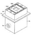
図1は、本発明のいくつかの実施形態による試験装置1の断面図を示す。試験装置1は、絶縁箱10、コンバータ12、チャック13、被試験体(DUT)15および試験盤19を含む。 FIG. 1 shows a cross-sectional view of a test apparatus 1 according to some embodiments of the present invention. The test apparatus 1 includes an
絶縁箱10は、第1の筺体10a(第1のカバー、下部筺体または下部カバーとも呼ばれる)および第2の筺体10b(第2のカバー、上部筺体または上部カバーとも呼ばれる)を含む。第1の筺体10aは、底面と、その底面の近くあるいは周りに設けられる側面を有する。第2の筺体10bは、上面と、その上面の近くあるいは周りに設けられる側面を有する。第1の筺体10aの側面は、第2の筺体10bの側面に対応して(例えば、連続して)設けられてDUT15と試験盤19を収容する空間10s(またはチャンバー)を形成する。第1の筺体10aと第2の筺体10bは緊密に接続され、外部の電磁波の放射が絶縁箱10に入り試験結果に影響を及ぼすことを防ぐ。第2の筺体10bは、その上面にチャック13を収容する開口または穴10bhを限定する。試験操作において、チャック13は、開口10bh内に配置されDUT15と接触する。 The
絶縁箱10は、第1の筺体10aの1つ以上の側面に配置されている接続部材10cと12を含む。例えば、接続部材10cと12は、第1の筺体10aの側面を貫通し、絶縁箱10の内部と絶縁箱10の外部の間に接続界面を形成し得る。いくつかの実施形態では、接続部材10cと接続部材12は、第1の筺体10aの同じ側面に配置されてもよい。あるいは、接続部材10cと接続部材12は、第1の筺体10aの異なる側面に配置される。いくつかの実施形態では、絶縁箱10は、設計の仕様によっては任意の数の接続部材を含むことがある。 The
いくつかの実施形態では、接続部材10cは、相対的な高周波信号(例えば、RF信号)を送信する。例えば、接続部材10cは、約500メガヘルツ(MHz)から約12ギガヘルツ(GHz)、約500MHzから約3GHz、約500MHzから約6GHz、約3GHzから約6GHz、および/または約6GHzから約12GHzの周波数の信号を送信する。例えば、接続部材10cはRFコネクタである。 In some embodiments, connecting
いくつかの実施形態では、接続部材12は、相対的な低周波信号または直流(DC)信号を送信する。例えば、接続12は、供給電力、デジタル信号などを送信する。例えば、接続部材10cは、約500MHzより低い低周波数の信号を送信する。例えば、接続部材12は、コンバータ、リレーまたはフィルタを含む。例えば、接続部材12は、低周波信号またはDC信号を送信するコネクタ(例えば、RS−232コネクタ)を備える回路基板であってもよい。 In some embodiments, the connecting
DUT15は試験盤19に配置されている。いくつかの実施形態では、DUT15は、高い周波数(例えば、約500MHzより高い周波数)で作動するチープまたはダイ付き回路、モジュールまたはデバイスである。DUT15は、例えば、ワイヤボンディング技術またはフリップチップ技術で試験盤19に電気的に接続されることができる。 The
試験盤19は、プリント回路基板(PCB)などの回路基板である。試験盤19は、単層のPCB、二層のPCBまたは多層のPCBであってもよい。いくつかの実施形態では、試験盤19は、FR−1回路基板、CEM−1回路基板、CEM−3回路基板、FR−4回路基板、またはほかの任意の適切な回路基板を含んでもよい。 The
試験盤19は、接続部材10cと高周波信号(例えば、RF信号)を送信または受信するDUT15のピンまたはノードに電気的に接続されている端子19aを含んでもよい。例えば、試験盤19の端子19aは、接続部材10cに電気的に接続されて、DUTから絶縁箱10の外部のデバイス(例えば、オシロスコープ、ベクトルネットワークアナライザ、スペクトラムアナライザなどの試験デバイス)へ高周波信号を送信するおよび/または絶縁箱10の外部のデバイスから高周波信号を受信する。 The
試験盤19は、接続部材12とDC信号または低周波信号(例えば、デジタル信号)を送信または受信するDUT15のピンまたはノードとに電気的に接続される端子19bを含んでもよい。例えば、試験盤19の端子19bは、接続部材12に電気的に接続されて、絶縁箱10の外部のデバイス(例えば、電源、デジタル制御回路など)から供給電力またはデジタル信号を受信するおよび/またはDUT15から絶縁箱10の外部のデバイスへ低周波信号を送信する。 The
図1に示すように、DUT15と試験盤19が絶縁箱10により覆われるか封入されるので、第1の筺体10aと第2の筺体10bにより限定される空間10sの幅W11または長さは、試験盤19の幅W12または長さの同等かそれ以上である。例えば、試験盤19の一端、または試験盤19の反対する両端は、筺体10と接触してもよい。例えば、空間10sの断面積は、試験盤19の断面積の同等かそれ以上である。これを可能にするのに、大きい絶縁箱10が実装されることがある。しかし、このような絶縁箱10は、DUT15の試験コストを増加させる。なお、絶縁箱10において試験盤19を支持するサポート(図1に図示せず)は、試験盤19の形状に合わせるために特製されることがある。したがって、異なる種類の試験盤が使用される場合に、サポートと絶縁箱は、試験盤19の形状とサイズに合わせるために変更されることがあり、またDUT15の試験コストを増加させる。 As shown in FIG. 1, since the
さらに、DUT15に電力またはデジタル信号を提供するために、接続部材12(例えば、コンバータ、リレーまたはフィルタ)は、絶縁箱10の第1の筺体10aの側面と一体になってもよい。しかし、外部のノイズまたは干渉は、接続部材12および/または接続部材12と第1の筺体10aの側面の間の空間を通って絶縁箱10に入ることがあり、試験結果に悪影響を及ぼす。また、接続部材12の設計は、試験盤の設計によって異なることがあるので、DUT15の試験コストを増加させる。 Further, in order to provide power or digital signals to the
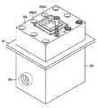
図2Aは、本発明のいくつかの実施形態による試験装置2の断面図を示す。試験装置2は、絶縁箱20、チャック23、被試験体(DUT)25および試験盤29を含む。 FIG. 2A shows a cross-sectional view of a test apparatus 2 according to some embodiments of the present invention. The test apparatus 2 includes an insulating box 20, a
絶縁箱20は、第1の筺体20a(第1のカバー、下部筺体または下部カバーとも呼ばれる)と、第1の筺体20aに連結される第2の筺体20b(第2のカバー、上部筺体または上部カバーとも呼ばれる)を含む。第1の筺体20aは、底面と、その底面の近くあるいは周りに設けられる側面を有する。第2の筺体20bは、上面と、その上面の近くあるいは周りに設けられる側面を有する。第1の筺体20aと第2の筺体20bは絶縁筺体であってもよい。第1の筺体20aの側面は、第2の筺体20bの側面に対応して(例えば、連続して)設けられて、DUT25と試験盤29の1つ以上の部分(例えば、部分291と292)を覆うか収容する空間20s(またはチャンバー)を形成し、また、試験盤29のほかの部分(例えば、部分293)を露出させる。第2の筺体20bは、その上面にチャック23を収容する開口または穴20bh1を限定する。試験操作において、チャック23は、チャック23と第2の筺体20bを緊密に封止するように、開口20bh1内に配置されDUT25と接触する。 The insulating box 20 includes a
第1の筺体20aと第2の筺体20bにより限定される空間20sの幅W21または長さは、試験盤29の幅W23または長さより短い(例えば、約0.95倍以下、約0.9倍以下、または約0.85倍以下で短い)。例えば、空間20sの断面積は、本発明のいくつかの実施形態による試験装置2の斜視図を示す図2Bに示すように、試験盤29の断面積より小さい(例えば、約0.95倍以下、約0.9倍以下、または約0.85倍以下で小さい)。また、第1の筺体20aの幅W22または長さも、試験盤29の幅W23または長さより短い(例えば、約0.95倍以下、約0.9倍以下、または約0.85倍以下で短い)。例えば、第1の筺体20aの底面の断面積は、図2Bに示すように、試験盤29の断面積より小さい(例えば、約0.95倍以下、約0.9倍以下、または約0.85倍以下で小さい)。 The width W21 or length of the
いくつかの実施形態では、第1の筺体20aは、その1つ以上の側壁の内面および/または試験盤29(例えば、試験盤29の部分292)と接触する表面に放射線吸収層20a1を含む。いくつかの実施形態では、第2の筺体20bは、その1つ以上の側壁の内面および/または試験盤29(例えば、試験盤29の部分292)と接触する表面に放射線吸収層20b1を含む。放射線吸収層20a1と20b1は、電磁波の放射が絶縁箱20に入ることを防ぐためのものである。 In some embodiments, the
絶縁箱20は、第1の筺体20aの1つ以上の側面に配置されている接続部材20cを含む。例えば、接続部材20cは、第1の筺体20aの側面を貫通して絶縁箱20の内部と絶縁箱20の外部の間に接続界面を形成し得る。いくつかの実施形態では、絶縁箱20は、設計の仕様によっては任意の数の接続部材を含んでもよい。いくつかの実施形態では、接続部材20cは、相対的な高周波信号(例えば、RF信号)を送信する。例えば、接続部材20cは、約500MHzから約12GHz、約500MHzから約3GHz、約500MHzから約6GHz、約3GHzから約6GHz、および/または約6GHzから約12GHzの周波数の信号を送信する。例えば、接続部材20cはRFコネクタである。 The insulating box 20 includes a
DUT25は試験盤29に配置されている。例えば、DUT25は、試験盤29の部分291に配置されている。いくつかの実施形態では、DUT25は、高い周波数(例えば、約500MHzより高い周波数)で作動するチープまたはダイ付き回路、モジュールまたはデバイスである。DUT25は、例えば、ワイヤボンディング技術またはフリップチップ技術で試験盤29に電気的に接続されることができる。 The
試験盤29は、プリント回路基板(PCB)などの回路基板を含む。試験盤29は、単層のPCB、二層のPCBまたは多層のPCBであってもよい。いくつかの実施形態では、試験盤29は、FR−1回路基板、CEM−1回路基板、CEM−3回路基板、FR−4回路基板、または任意のほかの適切な回路基板を含んでもよい。部分291が第1の筺体20aと第2の筺体により限定される空間20s内に配置され、部分293が絶縁箱20から露出されまたはその外部に位置し、部分292が部分291と293の間に配置されている。部分292は、第1の筺体20aおよび第2の筺体20bに接触するおよび/または放射線吸収層20a1および20b1に接触する。いくつかの実施形態では、試験盤29は、試験盤29の1つ以上の部分(例えば、部分291と293)を覆い、試験盤29のほかの部分(例えば、部分292)を露出させる保護層(例えば、ソルダマスク)29pを含む。 The
試験盤29は、試験盤29の部分291に配置されている端子29aを含んでもよい。端子29aは、接続部材20cと高周波信号(例えば、RF信号)を送信または受信するDUT25に電気的に接続されている。例えば、試験盤29の端子29aは、接続部材20cに電気的に接続されて、DUT25から絶縁箱20の外部のデバイス(例えば、オシロスコープ、ベクトルネットワークアナライザ、スペクトラムアナライザなどの試験デバイス)へ高周波信号を送信するおよび/または絶縁箱20の外部のデバイスから高周波信号を受信する。 The
試験盤29は、試験盤29の部分293に配置されている端子29bを含んでもよい。例えば、端子29bは、絶縁箱20から露出されまたはその外部に位置する。端子29bは、DC信号または低周波信号(例えば、デジタル信号)を送信または受信するDUT25のピンまたはノードに電気的に接続されている。例えば、試験盤29の端子29bは、外部のデバイス(例えば、電源、デジタル制御回路など)に電気的に接続されて、供給電力またはデジタル信号を受信するおよび/またはDUT25から外部のデバイスに低周波信号を送信する。 The
外部の干渉またはノイズが低周波信号またはDC信号に相対的小さい影響を及ぼすので、試験盤29の端子29bは、実質的な悪影響がない限り絶縁箱20の外部に配置されてもよい。言い換えれば、絶縁箱20は、DUT25と高周波信号を送信および/または受信する試験盤29の端子29aを覆い、DC信号および/または低周波信号を送信および/または受信する試験盤29の端子29bを露出させるように設計されることができる。したがって、図1の絶縁箱10に比べて、図2Aの絶縁箱20のサイズを著しく低減でき、絶縁箱20の製造コストを低減することができる。また、試験盤29は、第1の筺体20aと第2の筺体20bの間に挟まれるので、試験盤29を支持するサポートが省かれ、また、DUT25の試験コストを低減できる。 Since external interference or noise has a relatively small effect on the low frequency signal or DC signal, the terminal 29b of the
なお、絶縁箱20からのDC信号および/または低周波信号を送信するおよび/または受信する試験盤29の端子29bを露出させることにより、図1に示すような接続部材12(例えば、コンバータ、リレーまたはフィルタ)が省かれ、DUT25の試験コストを低減でき、また、外部ノイズまたは干渉がコンバータ、リレーまたはフィルタを通って絶縁箱20に入ることが防がれ、絶縁箱20の遮断性能を向上させることができる。いくつかの実施形態では、図1の絶縁箱10の遮断性能は約34.5dBから約44.8dBの範囲にあるが、図2の絶縁箱20の遮断性能は約74.2dBから約75.5dBの範囲にある。特に、接続部材12が配置される図1の絶縁箱10の側面の遮断性能は約34.5dBであるが、図2の絶縁箱20の側面の遮断性能は約74.2dBである。 1 is exposed by exposing a terminal 29b of a
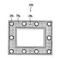
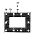
図3A、図3Bおよび図3Cは、本発明のいくつかの実施形態による異なる種類の試験盤(39A、39Bと39C)の上面図を示す。いくつかの実施形態では、試験盤39A、39Bおよび39Cは、図2Aと2Bに示すような試験装置2に使用されることができる。図3A、3Bおよび3Cに示すように、各々の試験盤39A、39Bおよび39Cは、試験盤39A、39Bおよび39Cの周縁に沿って配置される複数の穴29hを限定する。穴29hは、試験操作において試験盤39A、39Bおよび39Cの位置決めと締結の目的で、図2Bに示すように、第2の筺体20bの開口20bh2に対応して(例えば、隣接して)配置されている。また、各々の試験盤39A、39Bおよび39Cは複数の接地部材29gを含む。いくつかの実施形態では、接地部材は、図2Aの試験盤29の部分292に配置されるか、あるいは試験盤39A、39Bおよび39Cの対応する部分に配置される。接地部材29gは、試験盤29を貫通して試験盤29の上面から試験盤29の底面まで伸びる。いくつかの実施形態では、接地部材29は、絶縁箱20の遮断性能またはシールド性能を向上させるために、第1の筺体20aと第2の筺体20bに電気的に接続される。いくつかの実施形態では、各々の接地部材29の第1の部分がそれぞれ試験盤の底面から露出され、各々の接地部材29の第2の部分がそれぞれ試験盤の上面から露出され、第1の筺体20aが接地部材29のそれぞれの第1の部分と接触し、第2の筺体20bが接地部材29のそれぞれの第2の部分と接触する。 3A, 3B and 3C show top views of different types of test boards (39A, 39B and 39C) according to some embodiments of the present invention. In some embodiments,
いくつかの実施形態では、試験盤39A、39Bおよび39Cは異なる用途のために設計されることができる。例えば、試験盤39Aが約3GHz以下の周波数で作動するDUT25に適用でき、試験盤39Bが約6GHz以下の周波数で作動するDUT25に適用でき、試験盤39Cが約12GHz以下の周波数で作動するDUT25に適用できる。図3A、図3Bおよび図3Cに示すように、2つの隣接する接地部材29gの間の距離(またはピッチ)は、DUT25の操作周波数が増加するにつれて減少する。 In some embodiments,
図4A、図4Bおよび図4Cは、本発明のいくつかの実施形態による図2Aと図2Bに示すような試験装置2を操作する方法を示す。 4A, 4B and 4C illustrate a method of operating a test apparatus 2 as shown in FIGS. 2A and 2B according to some embodiments of the present invention.
図4Aを参照し、第1の筺体20aを設ける。図4Aに示すように、第1の筺体20aは、試験盤の位置決めと締結の目的で、配置された試験盤(例えば、試験盤29、39A、39Bおよび39C)の穴に対応する複数の穴20ahを限定する。 Referring to FIG. 4A, a
図4Bを参照し、試験盤29を第1の筺体20a上に置き、試験盤29の穴が第1の筺体20aの穴20ahに整列させる。そして、高周波信号を送信する試験盤29の端子(例えば、図2Aの端子29a)は、第1の筺体20aの側面に接続部材20cに電気的に接続されている。 Referring to FIG. 4B, the
その後、第2の筺体20bは、試験盤29に配置されてDUT25と試験盤29の1つ以上の部分(例えば、部分291と292)を覆い、試験盤29のほかの部分(例えば、部分293)を露出させる。また、試験盤29の穴は、第2の筺体20bの穴20bh2に整列させる。そして、第1の筺体20a、第2の筺体20bと試験盤29は、例えば、ねじ41またはほかの任意の適切な締め具により締められることがある。いくつかの実施形態では、試験盤29は、試験盤39A、39B、39Cとほかの任意の適切な試験盤に置き換えてもよい。 Thereafter, the
図4Cを参照し、第1の筺体20a、第2の筺体20bと試験盤29が締められた後に、チャック23は、チャック23と第2の筺体20bが緊密に封止されるように、第2の筺体20bの開口20bh1内に配置されDUT25と接触する。そして、接続部材20cは、試験デバイス(例えば、オシロスコープ、ベクトルネットワークアナライザ、スペクトラムアナライザなど)に電気的に接続されてDUT25に対して試験を行う。 Referring to FIG. 4C, after the
ここに使用される用語「ほぼ」、「実質的に」、「実質的な」および「約」は、小さな変動を説明し意味するのに使用される。事情または状況と併用される時に、それらの用語は、事情または状況がまさにそのとおりに起こる場合と、事情または状況が近似に生じる場合を言う。例えば、数値と併用される時に、それらの用語は、その数値の±10%以下、例えば、±5%以下、±4%以下、±3%以下、±2%以下、±1%以下、±0.5%以下、±0.1%以下、または±0.05%以下の変動の範囲を言う。例えば、2つの数値は、その差が平均値の±10%以下、例えば、±5%以下、±4%以下、±3%以下、±2%以下、±1%以下、±0.5%以下、±0.1%以下、または±0.05%以下であれば、「実質的に」同じであると見なされてもよい。 As used herein, the terms “approximately”, “substantially”, “substantial” and “about” are used to describe and imply small variations. When used in conjunction with a situation or situation, the terms refer to when the situation or situation occurs exactly as it is and when the situation or situation occurs approximately. For example, when used in conjunction with a numerical value, those terms are ± 10% or less of the numerical value, eg, ± 5% or less, ± 4% or less, ± 3% or less, ± 2% or less, ± 1% or less, ± A variation range of 0.5% or less, ± 0.1% or less, or ± 0.05% or less. For example, the difference between two numerical values is ± 10% or less of the average value, for example ± 5% or less, ± 4% or less, ± 3% or less, ± 2% or less, ± 1% or less, ± 0.5% Hereinafter, it may be considered “substantially” the same if it is ± 0.1% or less, or ± 0.05% or less.
2つの表面は、その2つの表面のずれが5μm以下、2μm以下、1μm以下、または0.5μm以下であれば、共平面または実質的に共平面であると見なされてもよい。 Two surfaces may be considered coplanar or substantially coplanar if the deviation between the two surfaces is 5 μm or less, 2 μm or less, 1 μm or less, or 0.5 μm or less.
いくつかの実施形態の説明では、部材がほかの部材の「上に」または「上方に」設けられることは、前者の部材が直接に後者の部材の上にある(例えば、物理接触がある)場合と、1つ以上の介在部材が前者の部材と後者の部材の間に位置する場合を含む。 In the description of some embodiments, a member is provided “on” or “above” another member so that the former member is directly on the latter member (eg, there is physical contact). And the case where one or more intervening members are located between the former member and the latter member.
ここに使用される用語「伝導性の」、「導電性の」および「導電性」は、電流を伝導する能力を言う。導電性の材料は、典型的に電流の流れに抵抗が小さいかあるいは抵抗がない材料を意味する。導電性の1つの測定単位として、メートルにつきシーメンス(S/m)が挙げられる。典型的には、導電性の材料は、ほぼ104S/m以上、例えば、少なくとも105S/mまたは少なくとも106S/mの導電性を有する材料である。材料の導電性は温度によって異なることがある。特に断りがない場合に、材料の導電性は室温で測定されたものである。The terms “conductive”, “conductive” and “conductive” as used herein refer to the ability to conduct current. By conductive material is meant a material that typically has little or no resistance to current flow. One unit of measurement for conductivity is Siemens (S / m) per meter. Typically, the conductive material is a material having a conductivity of approximately 104 S / m or more, eg, at least 105 S / m or at least 106 S / m. The conductivity of the material can vary with temperature. Unless otherwise noted, the conductivity of the material was measured at room temperature.
本発明は、その具体的な実施形態を参照しながら説明され図示されたが、それらの説明と図面は本発明を限定するものではない。添付の特許請求の範囲により限定される本発明の精神と範囲から逸脱することなく、実施形態において様々な変形が可能であり、等価部材に置換できることは、当業者にとって明らかである。図面は必ず縮尺にに一致するものとは限らない。製造プロセスにおける変動などにより、本発明の図面表現と実物の間に区別が発生することがある。具体的に図示されない本発明のほかの実施形態がある。仕様と図面は、限定性のものではなく、例示性のものと見なされる。本発明の目的、精神および範囲を逸脱することなく、特定の状況、材料、組成物、方法、またはプロセスに変更を施してもよい。すべてのこのような変更は添付の特許請求の範囲にあることを意図する。ここに開示される方法は特定の順序で行われる特定の操作を参照しながら説明されるが、これらの操作は、本発明の教示から逸脱することなく組み合わせ、細分され、または再順序付けられて等価方法を形成できると了承される。したがって、特にここに断りがない場合に、操作の順序と分類は、本発明を限定するものではない。 Although the invention has been described and illustrated with reference to specific embodiments thereof, the description and drawings are not intended to limit the invention. It will be apparent to those skilled in the art that various modifications and variations can be made in the embodiments without departing from the spirit and scope of the invention as defined by the appended claims. The drawings are not necessarily drawn to scale. Due to variations in the manufacturing process, a distinction may occur between the drawing representation of the present invention and the actual product. There are other embodiments of the invention that are not specifically illustrated. The specification and drawings are to be regarded as illustrative rather than restrictive. Changes may be made in the particular situation, material, composition, method, or process without departing from the purpose, spirit, and scope of the invention. All such modifications are intended to be within the scope of the appended claims. Although the methods disclosed herein are described with reference to specific operations performed in a specific order, these operations can be combined, subdivided, or reordered equivalently without departing from the teachings of the present invention. It is acknowledged that a method can be formed. Accordingly, unless otherwise noted herein, the order and classification of operations do not limit the invention.
Claims (20)
Translated fromJapanese前記第1の絶縁筺体に連結される第2の絶縁筺体と、を含む試験装置であって、
前記第1の絶縁筺体と前記第2の絶縁筺体は、試験盤の第1の部分を覆い、前記試験盤の第2の部分を露出させることを特徴とする試験装置。A first insulating housing;
A test apparatus comprising: a second insulating housing coupled to the first insulating housing,
The test apparatus according to claim 1, wherein the first insulating casing and the second insulating casing cover a first portion of the test board and expose the second portion of the test board.
前記第3の部分は、前記第2の絶縁筺体および前記第1の絶縁筺体と接触し、
前記第3の部分は、接地部材を含む、
請求項1に記載の試験装置。The test board further includes a third portion disposed between the first portion and the second portion,
The third portion is in contact with the second insulating housing and the first insulating housing;
The third portion includes a ground member.
The test apparatus according to claim 1.
前記第2の絶縁筺体は、前記試験盤の第3の部分に対向する第2の放射線吸収層を含む、
請求項7に記載の試験装置。The first insulating housing includes a first radiation absorbing layer facing a third portion of the test board,
The second insulating housing includes a second radiation absorbing layer facing a third portion of the test board.
The test apparatus according to claim 7.
前記第1の絶縁カバーに連結される第2の絶縁カバーと、を含む試験装置であって、
前記第1の絶縁カバーと前記第2の絶縁カバーが試験盤により分離されることを特徴とする試験装置。A first insulating cover;
A test apparatus including a second insulating cover coupled to the first insulating cover,
The test apparatus, wherein the first insulating cover and the second insulating cover are separated by a test board.
前記第1の絶縁カバーと前記第2の絶縁カバーにより限定される前記空間内に配置されている第1の部分と、
前記第1の絶縁カバーと前記第2の絶縁カバーから露出される第2の部分と、を含む請求項13に記載の試験装置。Space is limited by the first insulating cover and the second insulating cover, and the test board is
A first portion disposed in the space defined by the first insulating cover and the second insulating cover;
The test apparatus according to claim 13, comprising: the first insulating cover and a second portion exposed from the second insulating cover.
前記第3の部分は、前記第2の絶縁カバーおよび前記第1の絶縁カバーと接触し、
前記第3の部分は、複数の接地部材を含む、
請求項16に記載の試験装置。The test board further includes a third portion disposed between the first portion and the second portion,
The third portion is in contact with the second insulating cover and the first insulating cover;
The third portion includes a plurality of ground members.
The test apparatus according to claim 16.
前記第2の絶縁カバーは、前記試験盤の第3の部分に対向する第2の放射線吸収層を含む、
請求項18に記載の試験装置。The first insulating cover includes a first radiation absorbing layer facing a third portion of the test board,
The second insulating cover includes a second radiation absorbing layer facing the third portion of the test board.
The test apparatus according to claim 18.
The test apparatus according to claim 14, wherein the second portion of the test panel includes a first connection member, and the first connection member transmits or receives a signal having a frequency of 500 MHz or less.
Applications Claiming Priority (2)
| Application Number | Priority Date | Filing Date | Title |
|---|---|---|---|
| US15/956,703 | 2018-04-18 | ||
| US15/956,703US10753973B2 (en) | 2018-04-18 | 2018-04-18 | Test apparatus and method for operating the same |
Publications (1)
| Publication Number | Publication Date |
|---|---|
| JP2019191144Atrue JP2019191144A (en) | 2019-10-31 |
Family
ID=65035626
Family Applications (1)
| Application Number | Title | Priority Date | Filing Date |
|---|---|---|---|
| JP2018231502APendingJP2019191144A (en) | 2018-04-18 | 2018-12-11 | Test device and operation method of the same |
Country Status (4)
| Country | Link |
|---|---|
| US (1) | US10753973B2 (en) |
| JP (1) | JP2019191144A (en) |
| CN (2) | CN110389263A (en) |
| TW (2) | TWM569530U (en) |
Families Citing this family (3)
| Publication number | Priority date | Publication date | Assignee | Title |
|---|---|---|---|---|
| US10753973B2 (en)* | 2018-04-18 | 2020-08-25 | Ase Test, Inc. | Test apparatus and method for operating the same |
| CN110618372B (en)* | 2019-09-06 | 2021-12-17 | 苏州浪潮智能科技有限公司 | Immersion liquid cooling-based high-precision electrical loss testing device for PCB laminated board |
| CN118805089A (en)* | 2022-02-10 | 2024-10-18 | 基思利仪器有限责任公司 | Solderless high current, high voltage, high bandwidth test fixture |
Citations (6)
| Publication number | Priority date | Publication date | Assignee | Title |
|---|---|---|---|---|
| JPH08102592A (en)* | 1994-09-30 | 1996-04-16 | Hioki Ee Corp | Electromagnetic shield case for mounting board |
| JPH10142291A (en)* | 1996-11-13 | 1998-05-29 | Advantest Corp | Ic tester |
| JP2002141380A (en)* | 2000-11-06 | 2002-05-17 | Orion Mach Co Ltd | Inspection equipment for semiconductor wafer |
| JP2006047306A (en)* | 2004-07-30 | 2006-02-16 | Agilent Technol Inc | Method and apparatus for electromagnetic interference shielding in an automatic test system |
| US7023227B1 (en)* | 2002-02-12 | 2006-04-04 | National Semiconductor Corporation | Apparatus for socketing and testing integrated circuits and methods of operating the same |
| WO2009025070A1 (en)* | 2007-08-23 | 2009-02-26 | Advantest Corporation | Test system and daughter unit |
Family Cites Families (19)
| Publication number | Priority date | Publication date | Assignee | Title |
|---|---|---|---|---|
| JP3608289B2 (en)* | 1996-03-28 | 2005-01-05 | 安藤電気株式会社 | Shield box for air measurement and coaxial cable measurement |
| US6861857B2 (en)* | 2001-10-17 | 2005-03-01 | Gaylan W. Moushon | Apparatus and method for positioning an integrated circuit for test |
| US7256600B2 (en)* | 2004-12-21 | 2007-08-14 | Teradyne, Inc. | Method and system for testing semiconductor devices |
| TWM327525U (en)* | 2007-06-29 | 2008-02-21 | I Lai Test Probes And Test Fixtures Co Ltd | Testing tool of memory module |
| WO2011084518A2 (en)* | 2009-12-15 | 2011-07-14 | Bind Biosciences, Inc. | Therapeutic polymeric nanoparticles comprising corticosteroids and methods of making and using same |
| US8044673B1 (en)* | 2010-04-28 | 2011-10-25 | Lajos Burgyan | Method and apparatus for positioning and contacting singulated semiconductor dies |
| CN203151850U (en)* | 2013-02-16 | 2013-08-21 | 保定奥普节能科技股份有限公司 | Ballast with low conducted interference |
| US20150116161A1 (en)* | 2013-10-28 | 2015-04-30 | Skycross, Inc. | Antenna structures and methods thereof for determining a frequency offset based on a signal magnitude measurement |
| US9874602B2 (en)* | 2014-10-17 | 2018-01-23 | Nxp Usa, Inc. | Test board support platform for supporting a test board |
| CN104837327A (en)* | 2015-05-21 | 2015-08-12 | 小米科技有限责任公司 | Circuit protection structure and electronic device |
| KR102328101B1 (en)* | 2015-07-07 | 2021-11-17 | 삼성전자주식회사 | Probe card, thermal insulation cover assembly for probe card, and apparatus of testing semiconducotr device including the probe card |
| KR102332339B1 (en)* | 2015-07-08 | 2021-12-01 | 삼성전자주식회사 | Vacuum socket and semiconductor detecting device including the same |
| US10665942B2 (en)* | 2015-10-16 | 2020-05-26 | At&T Intellectual Property I, L.P. | Method and apparatus for adjusting wireless communications |
| CN109315011A (en)* | 2016-06-10 | 2019-02-05 | At&T知识产权部有限合伙公司 | Method and apparatus for radio distributed antenna system with clock reference |
| BR112018075611A2 (en)* | 2016-06-10 | 2019-08-20 | At & T Ip I Lp | network termination and methods for use with it |
| US10718805B2 (en)* | 2016-06-14 | 2020-07-21 | Micron Technology, Inc. | Apparatus and methods for testing devices |
| US10291311B2 (en)* | 2016-09-09 | 2019-05-14 | At&T Intellectual Property I, L.P. | Method and apparatus for mitigating a fault in a distributed antenna system |
| CN206341346U (en)* | 2016-12-29 | 2017-07-18 | 广州飞达音响股份有限公司 | A kind of linear array sound equipment power amplifier |
| US10753973B2 (en)* | 2018-04-18 | 2020-08-25 | Ase Test, Inc. | Test apparatus and method for operating the same |
- 2018
- 2018-04-18USUS15/956,703patent/US10753973B2/enactiveActive
- 2018-06-08TWTW107207680Upatent/TWM569530U/enunknown
- 2018-06-08CNCN201810585418.1Apatent/CN110389263A/enactivePending
- 2018-06-08CNCN201820883623.1Upatent/CN208488503U/enactiveActive
- 2018-06-08TWTW107119751Apatent/TWI808976B/enactive
- 2018-12-11JPJP2018231502Apatent/JP2019191144A/enactivePending
Patent Citations (6)
| Publication number | Priority date | Publication date | Assignee | Title |
|---|---|---|---|---|
| JPH08102592A (en)* | 1994-09-30 | 1996-04-16 | Hioki Ee Corp | Electromagnetic shield case for mounting board |
| JPH10142291A (en)* | 1996-11-13 | 1998-05-29 | Advantest Corp | Ic tester |
| JP2002141380A (en)* | 2000-11-06 | 2002-05-17 | Orion Mach Co Ltd | Inspection equipment for semiconductor wafer |
| US7023227B1 (en)* | 2002-02-12 | 2006-04-04 | National Semiconductor Corporation | Apparatus for socketing and testing integrated circuits and methods of operating the same |
| JP2006047306A (en)* | 2004-07-30 | 2006-02-16 | Agilent Technol Inc | Method and apparatus for electromagnetic interference shielding in an automatic test system |
| WO2009025070A1 (en)* | 2007-08-23 | 2009-02-26 | Advantest Corporation | Test system and daughter unit |
Also Published As
| Publication number | Publication date |
|---|---|
| TW201944761A (en) | 2019-11-16 |
| CN208488503U (en) | 2019-02-12 |
| US20190324082A1 (en) | 2019-10-24 |
| TWM569530U (en) | 2018-11-01 |
| CN110389263A (en) | 2019-10-29 |
| TWI808976B (en) | 2023-07-21 |
| US10753973B2 (en) | 2020-08-25 |
Similar Documents
| Publication | Publication Date | Title |
|---|---|---|
| AU2019215259B2 (en) | Radio frequency (RF) shielding structure for RF connector to microwave transmission interconnect regions and methods for manufacturing such RF shielding structure | |
| JP3415362B2 (en) | Impedance control interconnection device | |
| JP2019191144A (en) | Test device and operation method of the same | |
| US9660608B2 (en) | Low passive inter-modulation capacitor | |
| JP5323949B2 (en) | Mechanical and electrical connection device for coaxial cable for high-frequency signal transmission | |
| US10779395B1 (en) | Electromagnetic interference shield with integrated decoupling | |
| JP2011506925A (en) | ECO contactor | |
| US6818837B2 (en) | Wiring connection structure and transmitter using the same | |
| US11744057B1 (en) | Method and apparatus for a shielding structure of surface-mount devices | |
| CN104254945A (en) | Connection structure connecting high frequency circuit and waveguide, and manufacturing method for same | |
| KR20230127958A (en) | Radio-frequency arrangement having two interconnected radio-frequency components | |
| US11395418B2 (en) | Tuner module and receiving device | |
| JP2008263360A (en) | High frequency substrate equipment | |
| US12363875B2 (en) | Electronic assembly with electromagnetic shielding | |
| US6565385B1 (en) | Reducing electromagnetic emissions from a connector coupled to a printed circuit board | |
| KR102437243B1 (en) | Wireless communication apparatus capable of improving PIMD | |
| WO2020109649A1 (en) | Rf component |
Legal Events
| Date | Code | Title | Description |
|---|---|---|---|
| A521 | Request for written amendment filed | Free format text:JAPANESE INTERMEDIATE CODE: A523 Effective date:20181227 | |
| A621 | Written request for application examination | Free format text:JAPANESE INTERMEDIATE CODE: A621 Effective date:20211203 | |
| A977 | Report on retrieval | Free format text:JAPANESE INTERMEDIATE CODE: A971007 Effective date:20220331 | |
| A131 | Notification of reasons for refusal | Free format text:JAPANESE INTERMEDIATE CODE: A131 Effective date:20220405 | |
| A521 | Request for written amendment filed | Free format text:JAPANESE INTERMEDIATE CODE: A523 Effective date:20220705 | |
| A02 | Decision of refusal | Free format text:JAPANESE INTERMEDIATE CODE: A02 Effective date:20220920 |