JP2019144324A - Display device, and driver - Google Patents
Display device, and driverDownload PDFInfo
- Publication number
- JP2019144324A JP2019144324AJP2018026449AJP2018026449AJP2019144324AJP 2019144324 AJP2019144324 AJP 2019144324AJP 2018026449 AJP2018026449 AJP 2018026449AJP 2018026449 AJP2018026449 AJP 2018026449AJP 2019144324 AJP2019144324 AJP 2019144324A
- Authority
- JP
- Japan
- Prior art keywords
- signal line
- scanning signal
- transistor
- output
- display device
- Prior art date
- Legal status (The legal status is an assumption and is not a legal conclusion. Google has not performed a legal analysis and makes no representation as to the accuracy of the status listed.)
- Pending
Links
Images


Classifications
- G—PHYSICS
- G09—EDUCATION; CRYPTOGRAPHY; DISPLAY; ADVERTISING; SEALS
- G09G—ARRANGEMENTS OR CIRCUITS FOR CONTROL OF INDICATING DEVICES USING STATIC MEANS TO PRESENT VARIABLE INFORMATION
- G09G3/00—Control arrangements or circuits, of interest only in connection with visual indicators other than cathode-ray tubes
- G09G3/20—Control arrangements or circuits, of interest only in connection with visual indicators other than cathode-ray tubes for presentation of an assembly of a number of characters, e.g. a page, by composing the assembly by combination of individual elements arranged in a matrix no fixed position being assigned to or needed to be assigned to the individual characters or partial characters
- G09G3/22—Control arrangements or circuits, of interest only in connection with visual indicators other than cathode-ray tubes for presentation of an assembly of a number of characters, e.g. a page, by composing the assembly by combination of individual elements arranged in a matrix no fixed position being assigned to or needed to be assigned to the individual characters or partial characters using controlled light sources
- G09G3/30—Control arrangements or circuits, of interest only in connection with visual indicators other than cathode-ray tubes for presentation of an assembly of a number of characters, e.g. a page, by composing the assembly by combination of individual elements arranged in a matrix no fixed position being assigned to or needed to be assigned to the individual characters or partial characters using controlled light sources using electroluminescent panels
- G09G3/32—Control arrangements or circuits, of interest only in connection with visual indicators other than cathode-ray tubes for presentation of an assembly of a number of characters, e.g. a page, by composing the assembly by combination of individual elements arranged in a matrix no fixed position being assigned to or needed to be assigned to the individual characters or partial characters using controlled light sources using electroluminescent panels semiconductive, e.g. using light-emitting diodes [LED]
- G09G3/3208—Control arrangements or circuits, of interest only in connection with visual indicators other than cathode-ray tubes for presentation of an assembly of a number of characters, e.g. a page, by composing the assembly by combination of individual elements arranged in a matrix no fixed position being assigned to or needed to be assigned to the individual characters or partial characters using controlled light sources using electroluminescent panels semiconductive, e.g. using light-emitting diodes [LED] organic, e.g. using organic light-emitting diodes [OLED]
- G09G3/3266—Details of drivers for scan electrodes
- G—PHYSICS
- G09—EDUCATION; CRYPTOGRAPHY; DISPLAY; ADVERTISING; SEALS
- G09G—ARRANGEMENTS OR CIRCUITS FOR CONTROL OF INDICATING DEVICES USING STATIC MEANS TO PRESENT VARIABLE INFORMATION
- G09G3/00—Control arrangements or circuits, of interest only in connection with visual indicators other than cathode-ray tubes
- G09G3/20—Control arrangements or circuits, of interest only in connection with visual indicators other than cathode-ray tubes for presentation of an assembly of a number of characters, e.g. a page, by composing the assembly by combination of individual elements arranged in a matrix no fixed position being assigned to or needed to be assigned to the individual characters or partial characters
- G09G3/34—Control arrangements or circuits, of interest only in connection with visual indicators other than cathode-ray tubes for presentation of an assembly of a number of characters, e.g. a page, by composing the assembly by combination of individual elements arranged in a matrix no fixed position being assigned to or needed to be assigned to the individual characters or partial characters by control of light from an independent source
- G09G3/36—Control arrangements or circuits, of interest only in connection with visual indicators other than cathode-ray tubes for presentation of an assembly of a number of characters, e.g. a page, by composing the assembly by combination of individual elements arranged in a matrix no fixed position being assigned to or needed to be assigned to the individual characters or partial characters by control of light from an independent source using liquid crystals
- G09G3/3611—Control of matrices with row and column drivers
- G09G3/3674—Details of drivers for scan electrodes
- G09G3/3677—Details of drivers for scan electrodes suitable for active matrices only
- G—PHYSICS
- G09—EDUCATION; CRYPTOGRAPHY; DISPLAY; ADVERTISING; SEALS
- G09G—ARRANGEMENTS OR CIRCUITS FOR CONTROL OF INDICATING DEVICES USING STATIC MEANS TO PRESENT VARIABLE INFORMATION
- G09G2300/00—Aspects of the constitution of display devices
- G09G2300/04—Structural and physical details of display devices
- G—PHYSICS
- G09—EDUCATION; CRYPTOGRAPHY; DISPLAY; ADVERTISING; SEALS
- G09G—ARRANGEMENTS OR CIRCUITS FOR CONTROL OF INDICATING DEVICES USING STATIC MEANS TO PRESENT VARIABLE INFORMATION
- G09G2310/00—Command of the display device
- G09G2310/02—Addressing, scanning or driving the display screen or processing steps related thereto
- G09G2310/0264—Details of driving circuits
- G09G2310/0291—Details of output amplifiers or buffers arranged for use in a driving circuit
- G—PHYSICS
- G09—EDUCATION; CRYPTOGRAPHY; DISPLAY; ADVERTISING; SEALS
- G09G—ARRANGEMENTS OR CIRCUITS FOR CONTROL OF INDICATING DEVICES USING STATIC MEANS TO PRESENT VARIABLE INFORMATION
- G09G2310/00—Command of the display device
- G09G2310/06—Details of flat display driving waveforms
- G—PHYSICS
- G09—EDUCATION; CRYPTOGRAPHY; DISPLAY; ADVERTISING; SEALS
- G09G—ARRANGEMENTS OR CIRCUITS FOR CONTROL OF INDICATING DEVICES USING STATIC MEANS TO PRESENT VARIABLE INFORMATION
- G09G2320/00—Control of display operating conditions
- G09G2320/02—Improving the quality of display appearance
- G09G2320/0233—Improving the luminance or brightness uniformity across the screen
Landscapes
- Engineering & Computer Science (AREA)
- Physics & Mathematics (AREA)
- Computer Hardware Design (AREA)
- General Physics & Mathematics (AREA)
- Theoretical Computer Science (AREA)
- Chemical & Material Sciences (AREA)
- Crystallography & Structural Chemistry (AREA)
- Control Of Indicators Other Than Cathode Ray Tubes (AREA)
- Liquid Crystal Display Device Control (AREA)
- Devices For Indicating Variable Information By Combining Individual Elements (AREA)
Abstract
Translated fromJapaneseDescription
Translated fromJapanese本発明は表示デバイスに関する。 The present invention relates to a display device.
特許文献1には、異形(コーナを斜めに切り欠いた形状)の表示部の輝度ムラを抑える技術が開示されている。
特許文献1に記載の技術には、表示部の形状が制限されるのに加え、データ信号の調整が必要になるという問題がある。 The technique described in
本発明の一態様に係る表示デバイスは、複数のサブ画素に接続する第m走査信号線と、前記第m走査信号線よりも少ない数のサブ画素に接続する第n走査信号線と、複数段の出力回路を含み、前記第m走査信号線および前記第n走査信号線を駆動するドライバ回路とを備える表示デバイスであって、第m段の出力回路は、前記第m走査信号線に接続する第m出力トランジスタを含み、第n段の出力回路は、前記第n走査信号線に接続する第n出力トランジスタを含み、前記第n出力トランジスタは、前記第m出力トランジスタよりも駆動能力が小さい。 A display device according to one embodiment of the present invention includes an mth scan signal line connected to a plurality of subpixels, an nth scan signal line connected to a smaller number of subpixels than the mth scan signal line, and a plurality of stages. And a driver circuit that drives the m-th scanning signal line and the n-th scanning signal line, and the m-th stage output circuit is connected to the m-th scanning signal line. The m-th output transistor includes an n-th output transistor connected to the n-th scanning signal line, and the n-th output transistor has a driving capability smaller than that of the m-th output transistor.
本発明の一態様によれば、例えば異形の表示部の輝度ムラを抑えることができる。 According to one embodiment of the present invention, for example, luminance unevenness of an irregular display portion can be suppressed.
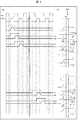
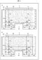
図1(a)は実施例1の表示デバイスの構成を示す模式図であり、図1(b)は表示デバイスの構成を示す断面図であり、図1(c)はサブ画素を示す回路図である。図1に示すように、表示デバイス2は、バックライトユニットBU、液晶パネルLP、ソースドライバSD、および表示制御回路DCCを備える。液晶パネルLPには、ゲートドライバGD1・GD2がモノリシックに形成される(GDM構造)。表示制御回路DCCは、ソースドライバSDおよびゲートドライバGD1・GD2を制御する。 FIG. 1A is a schematic diagram showing the configuration of the display device of Example 1, FIG. 1B is a cross-sectional view showing the configuration of the display device, and FIG. 1C is a circuit diagram showing sub-pixels. It is. As shown in FIG. 1, the
液晶パネルLPは、データ信号線DL、走査信号線Gm・Gn、ゲートドライバGD1・GD2を含むアクティブマトリクス基板3と、液晶層4と、カラーフィルタを含むカラーフィルタ基板5と、光学フィルム、タッチパネル等が含まれる機能層6とを備える。 The liquid crystal panel LP includes an
液晶パネルLPには切り欠き(ノッチ)NZが形成されており、異形の表示部DAには、複数のサブ画素(SPm・SPn・SPM・SPN)が設けられる。 A cutout (notch) NZ is formed in the liquid crystal panel LP, and a plurality of sub-pixels (SPm, SPn, SPM, SPN) are provided in the deformed display portion DA.
サブ画素SPi(i=m,n,M,N)は、画素トランジスタTRおよび画素電極PEを含み、第1方向D1に延伸する走査信号線Gi(i=m,n、M,N)と、第2方向D2に延伸するデータ信号線DLに接続する。具体的には、画素電極PEは画素トランジスタTRを介してデータ信号線DLに接続され、画素トランジスタTRのゲート電極が走査信号線Giに接続される。また、画素電極PEおよび共通電極com間に液晶容量Clcが形成され、画素電極PEおよび補助容量配線CSi間に補助容量Ccsが形成される。なお、補助容量配線CSiはアクティブマトリクス基板3に形成され、共通電極comはアクティブマトリクス基板3あるいはカラーフィルタ基板5に形成される。画素トランジスタのチャネルには、酸化物半導体(例えばIn−Ga−Zn−O系の半導体)、低温ポリシリコン(LTPS)等を用いることができる。 The sub-pixel SPi (i = m, n, M, N) includes the pixel transistor TR and the pixel electrode PE, and the scanning signal line Gi (i = m, n, M, N) extending in the first direction D1; Connected to the data signal line DL extending in the second direction D2. Specifically, the pixel electrode PE is connected to the data signal line DL via the pixel transistor TR, and the gate electrode of the pixel transistor TR is connected to the scanning signal line Gi. Further, a liquid crystal capacitor Clc is formed between the pixel electrode PE and the common electrode com, and an auxiliary capacitor Ccs is formed between the pixel electrode PE and the auxiliary capacitor line CSi. The auxiliary capacitance line CSi is formed on the
〔実施形態1〕
図1では、第2方向D2に延びるゲートドライバGD1・GD2が、表示部DAを取り囲む非表示部NAに設けられる。表示部DAには、切り欠きNZの第1方向D1に関する一方サイドに位置するサイド領域SA1および他方サイドに位置するサイド領域SA2、並びに切り欠きNZよりも内側(中央側)のメイン領域MAが含まれる。切り欠きNZと重なるように、カメラレンズ、各種センサ等を配することができる。
In FIG. 1, the gate drivers GD1 and GD2 extending in the second direction D2 are provided in the non-display area NA surrounding the display area DA. The display part DA includes a side region SA1 located on one side in the first direction D1 of the notch NZ, a side region SA2 located on the other side, and a main region MA on the inner side (center side) than the notch NZ. It is. A camera lens, various sensors, and the like can be arranged so as to overlap with the notch NZ.
走査信号線Gm(第m走査信号線)はメイン領域MAを通り、ゲートドライバGD1・GD2に接続される。走査信号線Gn(第n走査信号線)はサイド領域SA1を通り、ゲートドライバGD1に接続される。ゲートドライバGD1からみれば、走査信号線Gmはm番目(mは自然数)の走査信号線であり、走査信号線Gnはn番目(nはm以外の自然数)の走査信号線である。走査信号線GNはサイド領域SA2を通り、ゲートドライバGD2に接続される。走査信号線Gmは2つのゲートドライバGD1・GD2で駆動され、走査信号線Gnは1つのゲートドライバGD1で駆動されるが、走査信号線Gnに接続されるサブ画素の数は、走査信号線Gmに接続されるサブ画素の数の半分未満であるため、ゲートドライバGD1からみれば、走査信号線Gmよりも走査信号線Gnの方が低負荷(時定数が小さい)であり、同様に、ゲートドライバGD2からみれば、走査信号線Gmよりも走査信号線GNの方が低負荷である。 The scanning signal line Gm (m-th scanning signal line) passes through the main area MA and is connected to the gate drivers GD1 and GD2. The scanning signal line Gn (nth scanning signal line) passes through the side region SA1 and is connected to the gate driver GD1. When viewed from the gate driver GD1, the scanning signal line Gm is the mth (m is a natural number) scanning signal line, and the scanning signal line Gn is the nth (n is a natural number other than m) scanning signal line. The scanning signal line GN passes through the side region SA2 and is connected to the gate driver GD2. The scanning signal line Gm is driven by two gate drivers GD1 and GD2, and the scanning signal line Gn is driven by one gate driver GD1, but the number of sub-pixels connected to the scanning signal line Gn is the scanning signal line Gm. Therefore, the scanning signal line Gn has a lower load (smaller time constant) than the scanning signal line Gm, as seen from the gate driver GD1. From the viewpoint of the driver GD2, the scanning signal line GN has a lower load than the scanning signal line Gm.
図2(a)はドライバ(GD1)の構成を示す模式図であり、図2(b)は当該ドライバの動作を示すタイミングチャートである。図3(a)はドライバ(GD2)の構成を示す模式図であり、図3(b)は当該ドライバの動作を示すタイミングチャートであり、図4(a)(b)は実施形態1の出力回路の構成を示す説明図であり、図5は実施形態1の効果を示す波形図である。 FIG. 2A is a schematic diagram showing the configuration of the driver (GD1), and FIG. 2B is a timing chart showing the operation of the driver. 3A is a schematic diagram showing the configuration of the driver (GD2), FIG. 3B is a timing chart showing the operation of the driver, and FIGS. 4A and 4B are outputs of the first embodiment. FIG. 5 is an explanatory diagram showing a circuit configuration, and FIG. 5 is a waveform diagram showing the effect of the first embodiment.
実施形態1では、サイド領域を通る走査信号線Gn・GNが低負荷であることを考慮して、ゲートドライバGD1・GD2を、図2〜図4のように構成している。 In the first embodiment, the gate drivers GD1 and GD2 are configured as shown in FIGS. 2 to 4 in consideration that the scanning signal lines Gn and GN passing through the side regions have a low load.
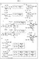
具体的には、ゲートドライバGD1は、複数段のフリップフロップおよび複数段の出力回路を含み、第m段のフリップフロップFmに接続する第m段の出力回路Xmは、走査信号線Gmに接続するトランジスタTm(出力トランジスタ)を含み、第n段のフリップフロップFnに接続する第n段の出力回路Xnは、走査信号線Gnに接続するトランジスタTn(出力トランジスタ)を含み、トランジスタTnは、トランジスタTmよりも駆動能力が小さい。トランジスタの駆動能力とは、ゲート・ソース間電圧を所定値にしたときのドレイン電流値である(駆動能力が大きいトランジスタはドレイン電流値が大きい)。 Specifically, the gate driver GD1 includes a plurality of stages of flip-flops and a plurality of stages of output circuits, and the m-th stage output circuit Xm connected to the m-th stage flip-flop Fm is connected to the scanning signal line Gm. The nth stage output circuit Xn including the transistor Tm (output transistor) and connected to the nth stage flip-flop Fn includes a transistor Tn (output transistor) connected to the scanning signal line Gn, and the transistor Tn includes the transistor Tm. The driving ability is smaller than that. The driving capability of a transistor is a drain current value when the gate-source voltage is set to a predetermined value (a transistor having a large driving capability has a large drain current value).
また、ゲートドライバGD2は、複数段のフリップフロップおよび複数段の出力回路を含み、第m段のフリップフロップFMに接続する第m段の出力回路XMは、走査信号線Gmに接続するトランジスタTM(出力トランジスタ)を含み、第n段のフリップフロップFNに接続する第n段の出力回路XNは、走査信号線GNに接続するトランジスタTN(出力トランジスタ)を含み、トランジスタTNは、トランジスタTMよりも駆動能力が小さい。 The gate driver GD2 includes a plurality of stages of flip-flops and a plurality of stages of output circuits. The m-th stage output circuit XM connected to the m-th stage flip-flop FM includes a transistor TM ( The n-th stage output circuit XN connected to the n-th flip-flop FN includes a transistor TN (output transistor) connected to the scanning signal line GN, and the transistor TN is driven more than the transistor TM. Small ability.
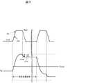
こうすれば、図2(b)、図3(b)および図5に示すように、出力回路Xnから走査信号線Gnに出力される走査パルスPnの戻り波形(図中にて破線で囲まれた立ち下がり波形)、および出力回路XNから走査信号線GNに出力される走査パルスPNの戻り波形を、出力回路Xmから走査信号線Gmに出力される走査パルスPmの戻り波形に揃えることができ、サイド領域SA1・SA2と、メイン領域MAとの輝度ムラを低減することができる。。 In this way, as shown in FIGS. 2B, 3B and 5, the return waveform of the scanning pulse Pn output from the output circuit Xn to the scanning signal line Gn (enclosed by a broken line in the figure). And the return waveform of the scan pulse PN output from the output circuit XN to the scan signal line GN can be aligned with the return waveform of the scan pulse Pm output from the output circuit Xm to the scan signal line Gm. Further, luminance unevenness between the side areas SA1 and SA2 and the main area MA can be reduced. .
図5に示すように、走査信号線Gmについては、走査パルスPmの戻り(立ち下がり)のタイミングで、画素電極PEの電圧VpがΔVmだけマイナス方向に引き込まれ、走査信号線Gnについては、走査パルスPnの戻り(立ち下がり)のタイミングで、画素電極PEの電圧VpがΔVnだけマイナス方向に引き込まれる。引き込み電圧ΔVm・ΔVnは、Cgd(走査信号線および画素電極間の寄生容量)に起因する。共通電極の電圧Vcomの最適値は引き込み電圧ΔVm・ΔVnに依存し、引き込み電圧ΔVm・ΔVnは走査パルスPm・Pnの戻り波形に依存するため、走査パルスPm・Pnの戻り波形を揃えることで、サイド領域SA1・SA2とメイン領域MAとでVcomの最適値が合致し、輝度ムラが抑制される。 As shown in FIG. 5, with respect to the scanning signal line Gm, the voltage Vp of the pixel electrode PE is drawn in the minus direction by ΔVm at the return (falling) timing of the scanning pulse Pm, and the scanning signal line Gn is scanned. At the return (falling) timing of the pulse Pn, the voltage Vp of the pixel electrode PE is pulled in the minus direction by ΔVn. The pull-in voltages ΔVm · ΔVn are caused by Cgd (parasitic capacitance between the scanning signal line and the pixel electrode). The optimum value of the common electrode voltage Vcom depends on the pull-in voltages ΔVm and ΔVn, and the pull-in voltages ΔVm and ΔVn depend on the return waveforms of the scan pulses Pm and Pn. Therefore, by aligning the return waveforms of the scan pulses Pm and Pn, The optimum value of Vcom is matched between the side areas SA1 and SA2 and the main area MA, and luminance unevenness is suppressed.
なお、出力回路Xn・XNを出力回路Xm・XMと同一構成とした場合は、図6のように、出力回路Xnからの走査パルスpnが、出力回路Xmからの走査パルスPmよりも急峻に戻る(ドロップする)ため、ΔVn>ΔVmとなり、サイド領域SA1・SA2のVcomの最適値が、メイン領域MAよりもマイナス方向にズレ、輝度ムラの発現、焼き付き(信頼性低下)のおそれがある。なお、Vcomの最適値のズレは画素電極PEに書き込むデータ信号側で調整することもできるが、この場合はソースドライバSDのカスタマイズが必要になるというデメリットがある。実施形態1ではアクティブマトリクス基板3におけるGDM(ゲートドライバモノリシック)の設計によって輝度ムラ対策ができるというメリットがある。 When the output circuits Xn and XN have the same configuration as the output circuits Xm and XM, as shown in FIG. 6, the scanning pulse pn from the output circuit Xn returns steeper than the scanning pulse Pm from the output circuit Xm. Therefore, ΔVn> ΔVm, and the optimum value of Vcom in the side areas SA1 and SA2 may be shifted in the negative direction from the main area MA, causing uneven brightness, and burn-in (decrease in reliability). The deviation of the optimum value of Vcom can be adjusted on the data signal side written to the pixel electrode PE, but in this case, there is a demerit that the source driver SD needs to be customized. The first embodiment is advantageous in that it is possible to take measures against luminance unevenness by designing a GDM (gate driver monolithic) in the
なお、例えば図2(a)のフリップフロップFmは、セット端子S、リセット端子R、および出力端子Qmを有するRSフリップフロップであり、出力端子Qmは出力回路Xmに接続され、出力回路Xmは、次段のフリップフロップFm+1のセット端子Sおよび前段のフリップフロップのリセット端子Rに接続される。 For example, the flip-flop Fm in FIG. 2A is an RS flip-flop having a set terminal S, a reset terminal R, and an output terminal Qm. The output terminal Qm is connected to the output circuit Xm. It is connected to the set terminal S of the next flip-flop Fm + 1 and the reset terminal R of the previous flip-flop.
図4(a)では、出力回路XmをnチャネルのトランジスタTm(出力トランジスタ)で構成し、トランジスタTmについては、ゲート端子をフリップフロップFmの出力Qmに接続し、一方の導通端子をクロック信号CKaの供給線に接続し、他方の導通端子を走査信号線Gmに接続する。また、出力回路XMをnチャネルのトランジスタTM(出力トランジスタ)で構成し、トランジスタTMについては、ゲート端子をフリップフロップFMの出力QMに接続し、一方の導通端子をクロック信号CKaの供給線に接続し、他方の導通端子を走査信号線Gmに接続する。また、出力回路XnをnチャネルのトランジスタTnで構成し、トランジスタTn(出力トランジスタ)については、ゲート端子をフリップフロップFnの出力Qnに接続し、一方の導通端子をクロック信号CKb(CKaとは逆位相)の供給線に接続し、他方の導通端子を走査信号線Gnに接続する。また、出力回路XNをnチャネルのトランジスタTN(出力トランジスタ)で構成し、トランジスタTNについては、ゲート端子をフリップフロップFNの出力QNに接続し、一方の導通端子をクロック信号CKbの供給線に接続し、他方の導通端子を走査信号線GNに接続する。 In FIG. 4A, the output circuit Xm is composed of an n-channel transistor Tm (output transistor), and for the transistor Tm, the gate terminal is connected to the output Qm of the flip-flop Fm, and one conduction terminal is connected to the clock signal CKa. The other conduction terminal is connected to the scanning signal line Gm. Further, the output circuit XM is composed of an n-channel transistor TM (output transistor). As for the transistor TM, the gate terminal is connected to the output QM of the flip-flop FM, and one conduction terminal is connected to the supply line of the clock signal CKa. Then, the other conduction terminal is connected to the scanning signal line Gm. Further, the output circuit Xn is composed of an n-channel transistor Tn. As for the transistor Tn (output transistor), the gate terminal is connected to the output Qn of the flip-flop Fn, and one conduction terminal is connected to the clock signal CKb (inverse of CKa). The other conduction terminal is connected to the scanning signal line Gn. Further, the output circuit XN is composed of an n-channel transistor TN (output transistor), and for the transistor TN, the gate terminal is connected to the output QN of the flip-flop FN, and one conduction terminal is connected to the supply line of the clock signal CKb. Then, the other conduction terminal is connected to the scanning signal line GN.
図4(a)では、フリップフロップの出力が「High」となっている状態で、クロック信号が「Low」から「High」になることで走査パルスが立ち上がる。クロック信号が「High」から「Low」になることで走査パルスが「High」から「Low」となる。 In FIG. 4A, the scanning pulse rises when the clock signal changes from “Low” to “High” while the output of the flip-flop is “High”. When the clock signal changes from “High” to “Low”, the scanning pulse changes from “High” to “Low”.
図4(a)では、トランジスタTmよりもトランジスタTnの駆動能力が小さく、トランジスタTMよりもトランジスタTNの駆動能力が小さい構成(具体例については後述)とする。 In FIG. 4A, the driving capability of the transistor Tn is smaller than that of the transistor Tm, and the driving capability of the transistor TN is smaller than that of the transistor TM (a specific example will be described later).
なお、図4(a)を図4(b)のように変形してもよい。具体的には、出力トランジスタ(Tm・TM・Tn・TN)のゲート端子(以下、ノードNdとする)と、フリップフロップの出力(Qm・QM・Qn・QN)との間にダイオード接続されたトランジスタTkを挿入し、ノードNdと走査信号線(Gm・GM・Gn・GN)との間にブートストラップ容量Cbを形成する。 Note that FIG. 4A may be modified as shown in FIG. Specifically, a diode connection is made between the gate terminal (hereinafter referred to as node Nd) of the output transistor (Tm · TM · Tn · TN) and the output (Qm · QM · Qn · QN) of the flip-flop. The transistor Tk is inserted, and a bootstrap capacitor Cb is formed between the node Nd and the scanning signal lines (Gm, GM, Gn, GN).
図4(b)の場合、フリップフロップの出力(Qm・QM・Qn・QN)が「High」になると、トランジスタTkを介してノードndがフリップフロップの出力電圧から閾値落ちした電位にプリチャージされる。その後、クロック信号が立ち上がると、ブートストラップ容量Cbを介してノードndが突き上げられる。この際、トランジスタTkはオフであってノードndがフローティングとなるので、ノードndはフリップフロップの出力電圧以上に突き上げられ、クロック信号の「High」レベルが閾値落ちすることなく走査信号線(Gm・GM・Gn・GN)に出力される。これにより、走査パルスの「High」レベルの低下を防ぐことができる。なお、ブートストラップ容量Cbは、容量素子でもよいし、出力トランジスタ(Tm・TM・Tn・TN)の寄生容量でもよい。 In the case of FIG. 4B, when the output (Qm, QM, Qn, QN) of the flip-flop becomes “High”, the node nd is precharged to a potential that is lower than the output voltage of the flip-flop via the transistor Tk. The Thereafter, when the clock signal rises, the node nd is pushed up via the bootstrap capacitor Cb. At this time, since the transistor Tk is off and the node nd is in a floating state, the node nd is pushed higher than the output voltage of the flip-flop, and the “High” level of the clock signal does not drop the threshold value. (GM · Gn · GN). As a result, it is possible to prevent the “High” level of the scan pulse from decreasing. The bootstrap capacitor Cb may be a capacitor element or a parasitic capacitor of an output transistor (Tm · TM · Tn · TN).
図4(c)では、出力回路Xmを、クロック信号CKaおよびフリップフロップFmの出力Qmが入力されるNAND、一方の導通端子がVdd(高電位側電源)に接続するpチャネルのトランジスタTp、およびnチャネルのトランジスタTmで構成し、トランジスタTmについては、ゲート端子をNANDの出力およびトランジスタTpのゲート端子に接続し、一方の導通端子をVss(低電位側電源)に接続し、他方の導通端子を、走査信号線GmおよびトランジスタTpの導通端子に接続する。また、出力回路XMを、クロック信号CKaおよびフリップフロップFMの出力QMが入力されるNAND、一方の導通端子がVdd(高電位側電源)に接続するpチャネルのトランジスタTp、およびnチャネルのトランジスタTMで構成し、トランジスタTMについては、ゲート端子をNANDの出力およびトランジスタTpのゲート端子に接続し、一方の導通端子をVssに接続し、他方の導通端子を、走査信号線GmおよびトランジスタTpの導通端子に接続する。また、出力回路Xnを、クロック信号CKbおよびフリップフロップFnの出力Qnが入力されるNAND、一方の導通端子がVddに接続するpチャネルのトランジスタTp、およびnチャネルのトランジスタTnで構成し、トランジスタTnについては、ゲート端子をNANDの出力およびトランジスタTpのゲート端子に接続し、一方の導通端子をVssに接続し、他方の導通端子を、走査信号線GnおよびトランジスタTpの導通端子に接続する。また、出力回路XNを、クロック信号CKbおよびフリップフロップFNの出力QNが入力されるNAND、一方の導通端子がVddに接続するpチャネルのトランジスタTp、およびnチャネルのトランジスタTNで構成し、トランジスタTNについては、ゲート端子をNANDの出力およびトランジスタTpのゲート端子に接続し、一方の導通端子をVssに接続し、他方の導通端子を、走査信号線GNおよびトランジスタTpの導通端子に接続する。 In FIG. 4C, the output circuit Xm is connected to a NAND to which the clock signal CKa and the output Qm of the flip-flop Fm are input, a p-channel transistor Tp whose one conduction terminal is connected to Vdd (high potential side power supply), and The transistor Tm is composed of an n-channel transistor Tm, the gate terminal of which is connected to the output of the NAND and the gate terminal of the transistor Tp, one conduction terminal is connected to Vss (low potential side power supply), and the other conduction terminal. Are connected to the scanning signal line Gm and the conduction terminal of the transistor Tp. The output circuit XM includes a NAND to which the clock signal CKa and the output QM of the flip-flop FM are input, a p-channel transistor Tp whose one conduction terminal is connected to Vdd (high potential side power supply), and an n-channel transistor TM. For the transistor TM, the gate terminal is connected to the NAND output and the gate terminal of the transistor Tp, one conduction terminal is connected to Vss, and the other conduction terminal is connected to the scanning signal line Gm and the transistor Tp. Connect to the terminal. The output circuit Xn includes a NAND to which the clock signal CKb and the output Qn of the flip-flop Fn are input, a p-channel transistor Tp whose one conduction terminal is connected to Vdd, and an n-channel transistor Tn. , The gate terminal is connected to the output of the NAND and the gate terminal of the transistor Tp, one conduction terminal is connected to Vss, and the other conduction terminal is connected to the scanning signal line Gn and the conduction terminal of the transistor Tp. The output circuit XN includes a NAND to which the clock signal CKb and the output QN of the flip-flop FN are input, a p-channel transistor Tp whose one conduction terminal is connected to Vdd, and an n-channel transistor TN. , The gate terminal is connected to the output of the NAND and the gate terminal of the transistor Tp, one conduction terminal is connected to Vss, and the other conduction terminal is connected to the scanning signal line GN and the conduction terminal of the transistor Tp.
図4(c)では、トランジスタTmよりもトランジスタTnの駆動能力が小さく、トランジスタTMよりもトランジスタTNの駆動能力が小さい構成(具体例については後述)とする。 In FIG. 4C, the driving capability of the transistor Tn is smaller than that of the transistor Tm, and the driving capability of the transistor TN is smaller than that of the transistor TM (a specific example will be described later).
図4(c)に示すNANDは、図4(d)に示すような、インバータin、アナログスイッチas、およびnチャネルのトランジスタTqを用いた回路で置き換えることができる。アナログスイッチasについては、2つの制御端子にフリップフロップの出力および反転出力を入力し、一方の導通端子にクロック信号を入力し、他方の導通端子をインバータivの入力端子に接続する。トランジスタTqについては、ゲート端子にフリップフロップの反転出力を入力し、一方の導通端子をVssに接続し、他方の導通端子を、インバータivの入力端子に接続する。 The NAND shown in FIG. 4C can be replaced with a circuit using an inverter in, an analog switch as, and an n-channel transistor Tq as shown in FIG. For the analog switch as, the output of the flip-flop and the inverted output are input to two control terminals, the clock signal is input to one conduction terminal, and the other conduction terminal is connected to the input terminal of the inverter iv. As for the transistor Tq, the inverted output of the flip-flop is input to the gate terminal, one conduction terminal is connected to Vss, and the other conduction terminal is connected to the input terminal of the inverter iv.
図4(e)では、出力回路Xmを、pチャネルのトランジスタTma(出力トランジスタ)およびnチャネルのトランジスタTmb(出力トランジスタ)の導通端子同士を接続して得られるCMOS型アナログスイッチで構成し、トランジスタTmaについては、ゲート端子をフリップフロップFmの出力Qmに接続し、一方の導通端子をクロック信号CKaの供給線に接続し、他方の導通端子を走査信号線Gmに接続する一方、トランジスタTmbについては、ゲート端子をフリップフロップFmの反転出力Qbmに接続し、一方の導通端子をクロック信号CKaの供給線に接続し、他方の導通端子を走査信号線Gmに接続する。また、出力回路XMを、pチャネルのトランジスタTMa(出力トランジスタ)およびnチャネルのトランジスタTMb(出力トランジスタ)の導通端子同士を接続して得られるCMOS型アナログスイッチで構成し、トランジスタTMaについては、ゲート端子をフリップフロップFMの出力QMに接続し、一方の導通端子をクロック信号CKaの供給線に接続し、他方の導通端子を走査信号線Gmに接続する一方、トランジスタTMbについては、ゲート端子をフリップフロップFMの反転出力QbMに接続し、一方の導通端子をクロック信号CKaの供給線に接続し、他方の導通端子を走査信号線Gmに接続する。また、出力回路Xnを、pチャネルのトランジスタTna(出力トランジスタ)およびnチャネルのトランジスタTnb(出力トランジスタ)の導通端子同士を接続して得られるCMOS型アナログスイッチで構成し、トランジスタTnaについては、ゲート端子をフリップフロップFnの出力Qnに接続し、一方の導通端子をクロック信号CKbの供給線に接続し、他方の導通端子を走査信号線Gnに接続する一方、トランジスタTnbについては、ゲート端子をフリップフロップFnの反転出力Qbnに接続し、一方の導通端子をクロック信号CKbの供給線に接続し、他方の導通端子を走査信号線Gnに接続する。また、出力回路XNを、pチャネルのトランジスタTNa(出力トランジスタ)およびnチャネルのトランジスタTNb(出力トランジスタ)の導通端子同士を接続して得られるCMOS型アナログスイッチで構成し、トランジスタTNaについては、ゲート端子をフリップフロップFNの出力QNに接続し、一方の導通端子をクロック信号CKbの供給線に接続し、他方の導通端子を走査信号線GNに接続する一方、トランジスタTNbについては、ゲート端子をフリップフロップFNの反転出力QbNに接続し、一方の導通端子をクロック信号CKbの供給線に接続し、他方の導通端子を走査信号線GNに接続する。 In FIG. 4E, the output circuit Xm is constituted by a CMOS type analog switch obtained by connecting the conduction terminals of a p-channel transistor Tma (output transistor) and an n-channel transistor Tmb (output transistor). For Tma, the gate terminal is connected to the output Qm of the flip-flop Fm, one conduction terminal is connected to the supply line of the clock signal CKa, and the other conduction terminal is connected to the scanning signal line Gm, while the transistor Tmb is The gate terminal is connected to the inverted output Qbm of the flip-flop Fm, one conduction terminal is connected to the supply line of the clock signal CKa, and the other conduction terminal is connected to the scanning signal line Gm. The output circuit XM is composed of a CMOS type analog switch obtained by connecting the conduction terminals of a p-channel transistor TMa (output transistor) and an n-channel transistor TMb (output transistor). The terminal is connected to the output QM of the flip-flop FM, one conduction terminal is connected to the supply line of the clock signal CKa, and the other conduction terminal is connected to the scanning signal line Gm, while the gate terminal of the transistor TMb is flip-flopped Is connected to the inverted output QbM of the clock FM, one conduction terminal is connected to the supply line of the clock signal CKa, and the other conduction terminal is connected to the scanning signal line Gm. The output circuit Xn is composed of a CMOS analog switch obtained by connecting the conduction terminals of a p-channel transistor Tna (output transistor) and an n-channel transistor Tnb (output transistor), and the transistor Tna has a gate The terminal is connected to the output Qn of the flip-flop Fn, one conduction terminal is connected to the supply line of the clock signal CKb, the other conduction terminal is connected to the scanning signal line Gn, and the gate terminal of the transistor Tnb is flip-flopped Fn is connected to the inverted output Qbn, one conduction terminal is connected to the supply line of the clock signal CKb, and the other conduction terminal is connected to the scanning signal line Gn. The output circuit XN is composed of a CMOS type analog switch obtained by connecting the conduction terminals of a p-channel transistor TNa (output transistor) and an n-channel transistor TNb (output transistor). The terminal is connected to the output QN of the flip-flop FN, one conduction terminal is connected to the supply line of the clock signal CKb, the other conduction terminal is connected to the scanning signal line GN, and the gate terminal of the transistor TNb is flip-flopped Is connected to the inverted output QbN of the clock FN, one conduction terminal is connected to the supply line of the clock signal CKb, and the other conduction terminal is connected to the scanning signal line GN.
図4(e)では、フリップフロップの出力が「High」、反転出力が「Low」となっている状態で、クロック信号が「Low」から「High」になることで走査パルスが立ち上がり、クロック信号が「High」から「Low」にとなることで走査パルスが戻る。 In FIG. 4E, when the output of the flip-flop is “High” and the inverted output is “Low”, the clock signal rises from “Low” to “High”, and the scan pulse rises. Changes from “High” to “Low” to return the scanning pulse.
図4(e)では、トランジスタTmaよりもトランジスタTnaの駆動能力が小さく、トランジスタTmbよりもトランジスタTnbの駆動能力が小さく、トランジスタTMaよりもトランジスタTNaの駆動能力が小さく、トランジスタTMbよりもトランジスタTNbの駆動能力が小さい構成(具体例については後述)とする。 In FIG. 4E, the driving capability of the transistor Tna is smaller than that of the transistor Tma, the driving capability of the transistor Tnb is smaller than that of the transistor Tmb, the driving capability of the transistor TNa is smaller than that of the transistor TMa, and the transistor TNb is smaller than that of the transistor TMb. It is assumed that the driving capability is small (specific examples will be described later).
なお、トランジスタTmaよりもトランジスタTnaの駆動能力が小さく、トランジスタTmbとトランジスタTnbの駆動能力が同等であり、トランジスタTMaよりもトランジスタTNaの駆動能力が小さく、トランジスタTMbとトランジスタTNbの駆動能力が同等である構成でもよい。また、トランジスタTmaとトランジスタTnaの駆動能力が同等で、トランジスタTmbよりもトランジスタTnbの駆動能力が小さく、トランジスタTMaとトランジスタTNaの駆動能力が同等で、トランジスタTMbよりもトランジスタTNbの駆動能力が小さい構成でもよい。トランジスタTna・Tnb・TNa・TNbの駆動能力については、走査パルスPnの立ち上がり波形および戻り波形が最適になるように決定すればよい。 Note that the driving capability of the transistor Tna is smaller than that of the transistor Tma, the driving capability of the transistor Tmb and the transistor Tnb is equal, the driving capability of the transistor TNa is smaller than that of the transistor TMa, and the driving capability of the transistor TMb and transistor TNb is equal. A certain configuration may be used. The transistor Tma and the transistor Tna have the same driving capability, the transistor Tnb has a lower driving capability than the transistor Tmb, the transistors TMa and the transistor TNa have the same driving capability, and the transistor TNb has a lower driving capability than the transistor TMb. But you can. The drive capability of the transistors Tna, Tnb, TNa, and TNb may be determined so that the rising waveform and the returning waveform of the scanning pulse Pn are optimized.
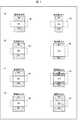
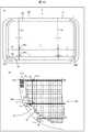
図7は、出力トランジスタの構成を示す平面図である。図7(a)〜図7(d)については、左側の(駆動能力大)構成が、図4のトランジスタ(出力トランジスタ)Tm・TM・Tma・Tmb・TMa・TMbに対応し、右側(駆動能力小)の構成が、図4のトランジスタ(出力トランジスタ)Tn・TN・Tna・Tnb・TNa・TNbに対応する。出力トランジスタは、アクティブマトリクス基板3の製造プロセスで形成され、そのチャネルには、酸化物半導体(例えばIn−Ga−Zn−O系の半導体)、低温ポリシリコン(LTPS)、アモルファスシリコン等を用いることができる。 FIG. 7 is a plan view showing the configuration of the output transistor. 7 (a) to 7 (d), the configuration on the left side (high driving capability) corresponds to the transistors (output transistors) Tm, TM, Tma, Tmb, TMa, and TMb in FIG. 4 corresponds to the transistors (output transistors) Tn, TN, Tna, Tnb, TNa, and TNb in FIG. The output transistor is formed by the manufacturing process of the
図7(a)では、ソース電極(ソース領域)SE、ドレイン電極(ドレイン領域)DEおよびチャネルCNを形成する際に、チャネル長を同一として、チャネル幅を小さくすることで駆動能力を小さくする(トランジスタのサイズも小さくなる)。図7(b)では、チャネル幅を同一として、チャネル長を長くすることで駆動能力を小さくする。図7(c)では、チャネル長およびチャネル幅を同一として、チャネルCNの両側に高抵抗領域HRを形成することで駆動能力を小さくする。図7(d)では、チャネル長およびチャネル幅を同一として、チャネルCNの不純物イオンのドーズ量を変えることで駆動能力を小さくする。 In FIG. 7A, when the source electrode (source region) SE, the drain electrode (drain region) DE, and the channel CN are formed, the channel length is the same and the driving capability is reduced by reducing the channel width ( The transistor size is also reduced). In FIG. 7B, the channel width is the same and the channel length is increased to reduce the driving capability. In FIG. 7C, the channel length and the channel width are the same, and the driving capability is reduced by forming the high resistance region HR on both sides of the channel CN. In FIG. 7D, the channel length and the channel width are the same, and the drive capability is reduced by changing the dose amount of the impurity ions in the channel CN.
図8は、実施形態1の表示デバイスの変形例を示す模式図である。図1(a)ではメイン領域MAを通る走査信号線Gmを2つのゲートドライバGD1・GD2に接続しているがこれに限定されない。図8(a)に示すように、各走査信号線を1つのゲートドライバ(GD1またはGD2)に接続する構成でもよい。この場合も、サイド領域を通る走査信号線Gn・GNが低負荷であるため、出力回路Xm・XM・Xn・XNを図4のように構成する。 FIG. 8 is a schematic diagram illustrating a modification of the display device according to the first embodiment. In FIG. 1A, the scanning signal line Gm passing through the main area MA is connected to the two gate drivers GD1 and GD2, but the present invention is not limited to this. As shown in FIG. 8A, the scanning signal lines may be connected to one gate driver (GD1 or GD2). Also in this case, since the scanning signal lines Gn and GN passing through the side region have a low load, the output circuits Xm, XM, Xn, and XN are configured as shown in FIG.
図1(a)ではゲートドライバGD1・GD2をアクティブマトリクス基板3にモノリシックに形成しているがこれに限定されない。図8(b)に示すように、ゲートドライバGD1・GD2を液晶パネルLPとは別のIC基板に設けることもできる。 In FIG. 1A, the gate drivers GD1 and GD2 are monolithically formed on the
図9は実施形態1の表示デバイスのさらなる変形例を示す模式図である。図9(a)に示すように、液晶パネルLP自体は矩形とし、表示部DAに切り欠きNZ(サブ画素が形成されない領域)を設けてもよいし、図9(b)に示すように、表示部DAに刳り貫きKZ(サブ画素が形成されない領域)を設けてもよい。これらの場合も、走査信号線Gnが走査信号線Gmよりも低負荷である(走査信号線Gnに接続するサブ画素が、走査信号線Gmに接続するサブ画素よりも少ない)ため、出力回路Xm・XM・Xn・XNを図4のように構成する。 FIG. 9 is a schematic view showing a further modification of the display device of the first embodiment. As shown in FIG. 9A, the liquid crystal panel LP itself may be rectangular, and a notch NZ (a region where no sub-pixel is formed) may be provided in the display unit DA. As shown in FIG. A KZ (a region where no sub-pixel is formed) may be provided through the display portion DA. Also in these cases, the scanning signal line Gn has a lower load than the scanning signal line Gm (the number of sub-pixels connected to the scanning signal line Gn is smaller than the sub-pixels connected to the scanning signal line Gm), so the output circuit Xm XM, Xn, and XN are configured as shown in FIG.
〔実施形態2〕
図10は実施形態2の表示デバイスの構成を示す模式図である。実施形態2では、図10(a)に示すように、走査信号線Gnが、サイド領域SA1・SA2を通り、2つのゲートドライバGD1・GD2に接続する構成とする。具体的には、走査信号線Gnに、切り欠きNZを避けるための迂回部Rsを設ける。この場合も、走査信号線Gnが走査信号線Gmよりも低負荷である(走査信号線Gnに接続するサブ画素が、走査信号線Gmに接続するサブ画素よりも少ない)ため、出力回路Xm・XM・Xn・XNを図4のように構成する。なお、図10(b)のように、各走査信号線を1つのゲートドライバ(GD1またはGD2)に接続する構成でもよい。[Embodiment 2]
FIG. 10 is a schematic diagram illustrating a configuration of a display device according to the second embodiment. In the second embodiment, as shown in FIG. 10A, the scanning signal line Gn passes through the side regions SA1 and SA2 and is connected to the two gate drivers GD1 and GD2. Specifically, a bypass portion Rs for avoiding the notch NZ is provided in the scanning signal line Gn. Also in this case, since the scanning signal line Gn has a lower load than the scanning signal line Gm (the number of subpixels connected to the scanning signal line Gn is smaller than the subpixel connected to the scanning signal line Gm), the output circuit Xm · XM, Xn, and XN are configured as shown in FIG. In addition, as shown in FIG. 10B, a configuration in which each scanning signal line is connected to one gate driver (GD1 or GD2) may be employed.
図11は、実施形態2の表示デバイスの変形例を示す模式図である。図11では、走査信号線Gnが、サイド領域SA1・SA2を通り、2つのゲートドライバGD1・GD2に接続する構成とし、切り欠きNZの近傍に、走査信号線Gnとの間で容量を形成する導電体Dzを設けることで、走査信号線Gnの負荷を調整(大きくする)ことができる。なお、導電体Dzには、共通電極の電圧Vcom等の定電位を供給する。なお、図11(b)のように、各走査信号線を1つのゲートドライバ(GD1またはGD2)に接続する構成でもよい。 FIG. 11 is a schematic diagram illustrating a modification of the display device according to the second embodiment. In FIG. 11, the scanning signal line Gn passes through the side regions SA1 and SA2 and is connected to the two gate drivers GD1 and GD2, and a capacitor is formed between the scanning signal line Gn and the notch NZ. By providing the conductor Dz, the load on the scanning signal line Gn can be adjusted (increased). Note that a constant potential such as a common electrode voltage Vcom is supplied to the conductor Dz. As shown in FIG. 11B, a configuration in which each scanning signal line is connected to one gate driver (GD1 or GD2) may be employed.
〔実施形態3〕
図12(a)は実施形態3の表示デバイスの構成を示す模式図であり、図12(b)は、表示部のコーナの拡大図である。図12のように、表示部DAのコーナを丸めて円弧状のエッジ(ラウンドエッジ)とする場合において、コーナ(切り欠きNZのサイド領域SA1)を通る走査信号線Gnの負荷は、コーナよりも中央側を通る走査信号線Gmよりも負荷が小さい、すなわち、走査信号線Gnに接続するサブ画素(サブ画素SPn含む)が、走査信号線Gmに接続するサブ画素(サブ画素SPm含む)よりも少ないため、出力回路Xm・Xnを図4のように構成する。[Embodiment 3]
FIG. 12A is a schematic diagram illustrating a configuration of the display device according to the third embodiment, and FIG. 12B is an enlarged view of a corner of the display unit. As shown in FIG. 12, when the corner of the display unit DA is rounded to form an arc-shaped edge (round edge), the load of the scanning signal line Gn passing through the corner (side area SA1 of the notch NZ) is larger than the corner. The load is smaller than the scanning signal line Gm passing through the center side, that is, the sub-pixel (including the sub-pixel SPn) connected to the scanning signal line Gn is smaller than the sub-pixel (including the sub-pixel SPm) connected to the scanning signal line Gm. Since there are few, the output circuit Xm * Xn is comprised like FIG.
表示部DAのコーナエッジKeを円弧状とする場合には、GDM構造のゲートドライバGD1の端部をコーナエッジKeに沿う(コーナエッジKeから等距離となる)ように形成するが、ゲートドライバGD1の端部に含まれる出力回路Xnを、図4および図7(a)のように構成する(例えば、トランジスタTnのチャネル幅を小さくする)ことで、出力回路Xnのサイズを出力回路Xmよりも小さくすることができる。こうすれば、横縞状の輝度ムラ(上下端部と中央部との輝度ムラ)を抑制しつつ、ゲートドライバGD1の端部(ラウンド部分)の形成領域を縮小させ、表示部DAを取り囲む非表示部(額縁領域)を小さくすることができる。図12(b)で示すコーナ以外の3つのコーナについても同様である。 When the corner edge Ke of the display section DA is formed in an arc shape, the end of the gate driver GD1 having the GDM structure is formed along the corner edge Ke (equal distance from the corner edge Ke), but the gate driver GD1. 4 is configured as shown in FIGS. 4 and 7A (for example, by reducing the channel width of the transistor Tn), the size of the output circuit Xn is made larger than that of the output circuit Xm. Can be small. In this way, while suppressing the horizontal stripe-shaped luminance unevenness (brightness unevenness between the upper and lower end portions and the central portion), the formation region of the end portion (round portion) of the gate driver GD1 is reduced, and the non-display surrounding the display portion DA The portion (frame area) can be reduced. The same applies to the three corners other than the corner shown in FIG.
なお、コーナを通る走査信号線Gnおよび走査信号線Guに関して、走査信号線Gnよりも外側を通る走査信号線Guの方が低負荷である(走査信号線Guに接続されるサブ画素の数は、走査信号線Gnに接続されるサブ画素の数よりも少ない)ことから、走査信号線Guに接続する出力回路Xuの出力トランジスタの駆動能力を出力回路Xnのそれよりも小さくすることもできる。なお、出力回路Xnに接続するフリップフロップFnと出力回路Xuに接続するフリップフロップFuとは、コーナエッジKeから等距離dをおいて配されている。 Regarding the scanning signal line Gn and the scanning signal line Gu passing through the corner, the scanning signal line Gu passing outside the scanning signal line Gn has a lower load (the number of sub-pixels connected to the scanning signal line Gu is Therefore, the driving capability of the output transistor of the output circuit Xu connected to the scanning signal line Gu can be made smaller than that of the output circuit Xn. The flip-flop Fn connected to the output circuit Xn and the flip-flop Fu connected to the output circuit Xu are arranged at an equal distance d from the corner edge Ke.
〔まとめ〕
本実施形態にかかる表示デバイスは、液晶ディスプレイに限られず、OLED(有機発光ダイオード)ディスプレイ、QLED(Quantum dot Light Emitting Diode)ディスプレイ等にも好適である。
〔態様1〕
複数のサブ画素に接続する第m走査信号線と、前記第m走査信号線よりも少ない数のサブ画素に接続する第n走査信号線と、複数段の出力回路を含み、前記第m走査信号線および前記第n走査信号線を駆動するドライバとを備える表示デバイスであって、第m段の出力回路は、前記第m走査信号線に接続する第m出力トランジスタを含み、第n段の出力回路は、前記第n走査信号線に接続する第n出力トランジスタを含み、前記第n出力トランジスタは、前記第m出力トランジスタよりも駆動能力が小さい表示デバイス。
〔態様2〕
切り欠きあるいは刳り貫きが形成された異形の表示部を備える例えば態様1記載の表示デバイス。
〔態様3〕
前記表示部は、前記切り欠きあるいは前記刳り貫きの一方サイドに位置するサイド領域を含み、前記第n走査信号線は前記サイド領域を通る例えば態様2記載の表示デバイス。
〔態様4〕
前記第n走査信号線と容量を形成し、定電圧が供給される導電体を備える例えば態様1〜3のいずれか1項に記載の表示デバイス。
〔態様5〕
前記第n出力トランジスタは、前記第m出力トランジスタよりもサイズが小さい例えば態様1〜4のいずれか1項に記載の表示デバイス。
〔態様6〕
前記表示部のコーナエッジが、曲線状あるいは前記第n走査信号線の延伸方向に対して斜線状であり、前記コーナエッジの外側には、前記ドライバの端部が、前記コーナエッジから等距離となるように形成され、前記ドライバの端部に前記第n段の出力回路が含まれる例えば態様2に記載の表示デバイス。
〔態様7〕
複数段の出力回路を含み、複数のサブ画素に接続する第m走査信号線と、前記第m走査信号線よりも少ない数のサブ画素に接続する第n走査信号線とを駆動するドライバであって、第n段の出力回路は、前記第n走査信号線に接続する第n出力トランジスタを含み、第m段の出力回路は、前記第m走査信号線に接続する第m出力トランジスタを含み、前記第n出力トランジスタは、前記第m出力トランジスタよりも駆動能力が小さいドライバ。[Summary]
The display device according to the present embodiment is not limited to a liquid crystal display, and is also suitable for an OLED (organic light emitting diode) display, a QLED (Quantum dot Light Emitting Diode) display, and the like.
[Aspect 1]
An m-th scanning signal line connected to a plurality of sub-pixels; an n-th scanning signal line connected to a smaller number of sub-pixels than the m-th scanning signal line; and a plurality of stages of output circuits. And a driver for driving the nth scanning signal line, wherein the mth stage output circuit includes an mth output transistor connected to the mth scanning signal line, and an nth stage output. The circuit includes an n-th output transistor connected to the n-th scanning signal line, and the n-th output transistor has a smaller driving capability than the m-th output transistor.
[Aspect 2]
A display device according to, for example,
[Aspect 3]
The display device according to
[Aspect 4]
The display device according to any one of
[Aspect 5]
The display device according to any one of
[Aspect 6]
The corner edge of the display section is curved or oblique with respect to the extending direction of the nth scanning signal line, and the end of the driver is equidistant from the corner edge outside the corner edge. The display device according to
[Aspect 7]
A driver including a plurality of stages of output circuits and driving an mth scanning signal line connected to a plurality of subpixels and an nth scanning signal line connected to a smaller number of subpixels than the mth scanning signal line. The nth stage output circuit includes an nth output transistor connected to the nth scanning signal line, and the mth stage output circuit includes an mth output transistor connected to the mth scanning signal line, The n-th output transistor is a driver having a driving capability smaller than that of the m-th output transistor.
2 表示デバイス
SPm・SPn サブ画素
Gm・Gn 走査信号線
Xm・Xn 出力回路
Tm・Tn (出力)トランジスタ
SA1・SA2 サイド領域
NZ 切り欠き2 Display device SPm / SPn Subpixel Gm / Gn Scanning signal line Xm / Xn Output circuit Tm / Tn (Output) Transistor SA1 / SA2 Side region NZ Notch
Claims (7)
Translated fromJapanese第m段の出力回路は、前記第m走査信号線に接続する第m出力トランジスタを含み、第n段の出力回路は、前記第n走査信号線に接続する第n出力トランジスタを含み、
前記第n出力トランジスタは、前記第m出力トランジスタよりも駆動能力が小さい表示デバイス。An m-th scanning signal line connected to a plurality of sub-pixels; an n-th scanning signal line connected to a smaller number of sub-pixels than the m-th scanning signal line; and a plurality of stages of output circuits. A display device comprising a line and a driver for driving the nth scanning signal line,
The m-th stage output circuit includes an m-th output transistor connected to the m-th scanning signal line, and the n-th stage output circuit includes an n-th output transistor connected to the n-th scanning signal line,
The n-th output transistor is a display device having a driving capability smaller than that of the m-th output transistor.
前記コーナエッジの外側には、前記ドライバの端部が、前記コーナエッジから等距離となるように形成され、
前記ドライバの端部に前記第n段の出力回路が含まれる請求項2に記載の表示デバイス。The corner edge of the display unit is curved or oblique with respect to the extending direction of the nth scanning signal line,
Outside the corner edge, the end of the driver is formed to be equidistant from the corner edge,
The display device according to claim 2, wherein the output circuit of the nth stage is included at an end of the driver.
第n段の出力回路は、前記第n走査信号線に接続する第n出力トランジスタを含み、第m段の出力回路は、前記第m走査信号線に接続する第m出力トランジスタを含み、
前記第n出力トランジスタは、前記第m出力トランジスタよりも駆動能力が小さいドライバ。A driver including a plurality of stages of output circuits and driving an mth scanning signal line connected to a plurality of subpixels and an nth scanning signal line connected to a smaller number of subpixels than the mth scanning signal line. And
The nth stage output circuit includes an nth output transistor connected to the nth scanning signal line, and the mth stage output circuit includes an mth output transistor connected to the mth scanning signal line,
The n-th output transistor is a driver having a driving capability smaller than that of the m-th output transistor.
Priority Applications (3)
| Application Number | Priority Date | Filing Date | Title |
|---|---|---|---|
| JP2018026449AJP2019144324A (en) | 2018-02-16 | 2018-02-16 | Display device, and driver |
| US16/238,546US20190259347A1 (en) | 2018-02-16 | 2019-01-03 | Display device and driver |
| CN201910034231.7ACN110164390A (en) | 2018-02-16 | 2019-01-15 | Show equipment, driver |
Applications Claiming Priority (1)
| Application Number | Priority Date | Filing Date | Title |
|---|---|---|---|
| JP2018026449AJP2019144324A (en) | 2018-02-16 | 2018-02-16 | Display device, and driver |
Publications (1)
| Publication Number | Publication Date |
|---|---|
| JP2019144324Atrue JP2019144324A (en) | 2019-08-29 |
Family
ID=67618052
Family Applications (1)
| Application Number | Title | Priority Date | Filing Date |
|---|---|---|---|
| JP2018026449APendingJP2019144324A (en) | 2018-02-16 | 2018-02-16 | Display device, and driver |
Country Status (3)
| Country | Link |
|---|---|
| US (1) | US20190259347A1 (en) |
| JP (1) | JP2019144324A (en) |
| CN (1) | CN110164390A (en) |
Families Citing this family (2)
| Publication number | Priority date | Publication date | Assignee | Title |
|---|---|---|---|---|
| CN108320693B (en)* | 2018-02-27 | 2022-04-19 | 京东方科技集团股份有限公司 | Grid driving circuit and driving method thereof, array substrate and display device |
| CN109904214B (en)* | 2019-03-29 | 2021-01-29 | 上海天马有机发光显示技术有限公司 | Display panel and display device comprising same |
Citations (5)
| Publication number | Priority date | Publication date | Assignee | Title |
|---|---|---|---|---|
| WO2009054166A1 (en)* | 2007-10-24 | 2009-04-30 | Sharp Kabushiki Kaisha | Display panel and display |
| JP2016148751A (en)* | 2015-02-12 | 2016-08-18 | 株式会社ジャパンディスプレイ | Display device |
| WO2017172375A1 (en)* | 2016-03-28 | 2017-10-05 | Groturbel Research Llc | Light-emitting diode displays |
| US20170337877A1 (en)* | 2016-05-19 | 2017-11-23 | Samsung Display Co., Ltd. | Display device |
| WO2018030207A1 (en)* | 2016-08-08 | 2018-02-15 | シャープ株式会社 | Display device |
Family Cites Families (6)
| Publication number | Priority date | Publication date | Assignee | Title |
|---|---|---|---|---|
| JP5210478B2 (en)* | 2001-08-31 | 2013-06-12 | 株式会社半導体エネルギー研究所 | Display device |
| CN100476909C (en)* | 2004-08-10 | 2009-04-08 | 精工爱普生株式会社 | Electro-optic device substrate, detection method thereof, electro-optic device and electronic equipment |
| KR100685814B1 (en)* | 2005-02-18 | 2007-02-22 | 삼성에스디아이 주식회사 | Scan driver and flat panel display with same |
| KR20080065458A (en)* | 2007-01-09 | 2008-07-14 | 삼성전자주식회사 | Display apparatus, control method thereof, and driving device for display panel |
| CN105788518B (en)* | 2014-12-25 | 2018-06-12 | 昆山工研院新型平板显示技术中心有限公司 | The uneven method and device compensated of display, display to display |
| CN107481669A (en)* | 2017-09-08 | 2017-12-15 | 武汉天马微电子有限公司 | Display panel and display device |
- 2018
- 2018-02-16JPJP2018026449Apatent/JP2019144324A/enactivePending
- 2019
- 2019-01-03USUS16/238,546patent/US20190259347A1/ennot_activeAbandoned
- 2019-01-15CNCN201910034231.7Apatent/CN110164390A/enactivePending
Patent Citations (5)
| Publication number | Priority date | Publication date | Assignee | Title |
|---|---|---|---|---|
| WO2009054166A1 (en)* | 2007-10-24 | 2009-04-30 | Sharp Kabushiki Kaisha | Display panel and display |
| JP2016148751A (en)* | 2015-02-12 | 2016-08-18 | 株式会社ジャパンディスプレイ | Display device |
| WO2017172375A1 (en)* | 2016-03-28 | 2017-10-05 | Groturbel Research Llc | Light-emitting diode displays |
| US20170337877A1 (en)* | 2016-05-19 | 2017-11-23 | Samsung Display Co., Ltd. | Display device |
| WO2018030207A1 (en)* | 2016-08-08 | 2018-02-15 | シャープ株式会社 | Display device |
Also Published As
| Publication number | Publication date |
|---|---|
| US20190259347A1 (en) | 2019-08-22 |
| CN110164390A (en) | 2019-08-23 |
Similar Documents
| Publication | Publication Date | Title |
|---|---|---|
| US12232385B2 (en) | Display substrate and display panel | |
| US10901442B2 (en) | Active-matrix substrate, display panel and display device including the same | |
| KR102360787B1 (en) | Built-in gate driver and display device using the same | |
| EP4068263B1 (en) | Shift register circuit and method for driving same, and gate driving circuit and display apparatus | |
| KR101409110B1 (en) | Display device | |
| CN111868807B (en) | display device | |
| CN101334983B (en) | Liquid crystal device and electronic apparatus | |
| US20190259345A1 (en) | Display panel | |
| KR102045730B1 (en) | Inverter and driving circuit and display device using the same | |
| CN102834871A (en) | Shift register | |
| CN106233368A (en) | Display device | |
| TW200919435A (en) | Electro-optical device, driving circuit, and electronic apparatus | |
| JP2019144325A (en) | Display panel | |
| CN111971729A (en) | Display device | |
| CN102714220B (en) | Shift register and display apparatus | |
| US10679578B2 (en) | Display device having driving circuitry with driving gate lines | |
| JP2019144324A (en) | Display device, and driver | |
| US11562707B2 (en) | Liquid crystal display device configured for speeding up gate drive of pixel transistors | |
| KR102416888B1 (en) | Display panel | |
| KR102587318B1 (en) | Gate driving circuit and display device having the same | |
| KR102175405B1 (en) | Shift resister | |
| US8665408B2 (en) | Liquid crystal display device | |
| JP2009162983A (en) | Electro-optical device, driving circuit, driving method, and electronic device | |
| KR20240113001A (en) | Scan signal driver and display device including the same | |
| JP2023142982A (en) | display device |
Legal Events
| Date | Code | Title | Description |
|---|---|---|---|
| A621 | Written request for application examination | Free format text:JAPANESE INTERMEDIATE CODE: A621 Effective date:20190111 | |
| A977 | Report on retrieval | Free format text:JAPANESE INTERMEDIATE CODE: A971007 Effective date:20190912 | |
| A131 | Notification of reasons for refusal | Free format text:JAPANESE INTERMEDIATE CODE: A131 Effective date:20191008 | |
| A02 | Decision of refusal | Free format text:JAPANESE INTERMEDIATE CODE: A02 Effective date:20200414 |