JP2019126074A - Interface circuit and information processing system - Google Patents
Interface circuit and information processing systemDownload PDFInfo
- Publication number
- JP2019126074A JP2019126074AJP2019040332AJP2019040332AJP2019126074AJP 2019126074 AJP2019126074 AJP 2019126074AJP 2019040332 AJP2019040332 AJP 2019040332AJP 2019040332 AJP2019040332 AJP 2019040332AJP 2019126074 AJP2019126074 AJP 2019126074A
- Authority
- JP
- Japan
- Prior art keywords
- signal
- transmission
- interface circuit
- external device
- differential
- Prior art date
- Legal status (The legal status is an assumption and is not a legal conclusion. Google has not performed a legal analysis and makes no representation as to the accuracy of the status listed.)
- Granted
Links
Images


Classifications
- H—ELECTRICITY
- H04—ELECTRIC COMMUNICATION TECHNIQUE
- H04L—TRANSMISSION OF DIGITAL INFORMATION, e.g. TELEGRAPHIC COMMUNICATION
- H04L5/00—Arrangements affording multiple use of the transmission path
- H04L5/02—Channels characterised by the type of signal
- G—PHYSICS
- G09—EDUCATION; CRYPTOGRAPHY; DISPLAY; ADVERTISING; SEALS
- G09G—ARRANGEMENTS OR CIRCUITS FOR CONTROL OF INDICATING DEVICES USING STATIC MEANS TO PRESENT VARIABLE INFORMATION
- G09G5/00—Control arrangements or circuits for visual indicators common to cathode-ray tube indicators and other visual indicators
- G09G5/003—Details of a display terminal, the details relating to the control arrangement of the display terminal and to the interfaces thereto
- G09G5/006—Details of the interface to the display terminal
- G09G5/008—Clock recovery
- H—ELECTRICITY
- H04—ELECTRIC COMMUNICATION TECHNIQUE
- H04L—TRANSMISSION OF DIGITAL INFORMATION, e.g. TELEGRAPHIC COMMUNICATION
- H04L25/00—Baseband systems
- H04L25/02—Details ; arrangements for supplying electrical power along data transmission lines
- H04L25/0264—Arrangements for coupling to transmission lines
- H04L25/0272—Arrangements for coupling to multiple lines, e.g. for differential transmission
- H—ELECTRICITY
- H04—ELECTRIC COMMUNICATION TECHNIQUE
- H04L—TRANSMISSION OF DIGITAL INFORMATION, e.g. TELEGRAPHIC COMMUNICATION
- H04L25/00—Baseband systems
- H04L25/02—Details ; arrangements for supplying electrical power along data transmission lines
- H04L25/14—Channel dividing arrangements, i.e. in which a single bit stream is divided between several baseband channels and reassembled at the receiver
- H—ELECTRICITY
- H04—ELECTRIC COMMUNICATION TECHNIQUE
- H04L—TRANSMISSION OF DIGITAL INFORMATION, e.g. TELEGRAPHIC COMMUNICATION
- H04L5/00—Arrangements affording multiple use of the transmission path
- H04L5/22—Arrangements affording multiple use of the transmission path using time-division multiplexing
- H—ELECTRICITY
- H04—ELECTRIC COMMUNICATION TECHNIQUE
- H04L—TRANSMISSION OF DIGITAL INFORMATION, e.g. TELEGRAPHIC COMMUNICATION
- H04L9/00—Cryptographic mechanisms or cryptographic arrangements for secret or secure communications; Network security protocols
- H04L9/08—Key distribution or management, e.g. generation, sharing or updating, of cryptographic keys or passwords
- H04L9/0816—Key establishment, i.e. cryptographic processes or cryptographic protocols whereby a shared secret becomes available to two or more parties, for subsequent use
- H04L9/0819—Key transport or distribution, i.e. key establishment techniques where one party creates or otherwise obtains a secret value, and securely transfers it to the other(s)
- H04L9/0825—Key transport or distribution, i.e. key establishment techniques where one party creates or otherwise obtains a secret value, and securely transfers it to the other(s) using asymmetric-key encryption or public key infrastructure [PKI], e.g. key signature or public key certificates
- H—ELECTRICITY
- H04—ELECTRIC COMMUNICATION TECHNIQUE
- H04N—PICTORIAL COMMUNICATION, e.g. TELEVISION
- H04N21/00—Selective content distribution, e.g. interactive television or video on demand [VOD]
- H04N21/40—Client devices specifically adapted for the reception of or interaction with content, e.g. set-top-box [STB]; Operations thereof
- H04N21/43—Processing of content or additional data, e.g. demultiplexing additional data from a digital video stream; Elementary client operations, e.g. monitoring of home network or synchronising decoder's clock; Client middleware
- H04N21/436—Interfacing a local distribution network, e.g. communicating with another STB or one or more peripheral devices inside the home
- H04N21/4363—Adapting the video stream to a specific local network, e.g. a Bluetooth® network
- H04N21/43632—Adapting the video stream to a specific local network, e.g. a Bluetooth® network involving a wired protocol, e.g. IEEE 1394
- H04N21/43635—HDMI
- H—ELECTRICITY
- H04—ELECTRIC COMMUNICATION TECHNIQUE
- H04N—PICTORIAL COMMUNICATION, e.g. TELEVISION
- H04N5/00—Details of television systems
- H04N5/44—Receiver circuitry for the reception of television signals according to analogue transmission standards
- G—PHYSICS
- G09—EDUCATION; CRYPTOGRAPHY; DISPLAY; ADVERTISING; SEALS
- G09G—ARRANGEMENTS OR CIRCUITS FOR CONTROL OF INDICATING DEVICES USING STATIC MEANS TO PRESENT VARIABLE INFORMATION
- G09G2370/00—Aspects of data communication
- G09G2370/04—Exchange of auxiliary data, i.e. other than image data, between monitor and graphics controller
- G09G2370/042—Exchange of auxiliary data, i.e. other than image data, between monitor and graphics controller for monitor identification
- G—PHYSICS
- G09—EDUCATION; CRYPTOGRAPHY; DISPLAY; ADVERTISING; SEALS
- G09G—ARRANGEMENTS OR CIRCUITS FOR CONTROL OF INDICATING DEVICES USING STATIC MEANS TO PRESENT VARIABLE INFORMATION
- G09G2370/00—Aspects of data communication
- G09G2370/04—Exchange of auxiliary data, i.e. other than image data, between monitor and graphics controller
- G09G2370/045—Exchange of auxiliary data, i.e. other than image data, between monitor and graphics controller using multiple communication channels, e.g. parallel and serial
- G09G2370/047—Exchange of auxiliary data, i.e. other than image data, between monitor and graphics controller using multiple communication channels, e.g. parallel and serial using display data channel standard [DDC] communication
- G—PHYSICS
- G09—EDUCATION; CRYPTOGRAPHY; DISPLAY; ADVERTISING; SEALS
- G09G—ARRANGEMENTS OR CIRCUITS FOR CONTROL OF INDICATING DEVICES USING STATIC MEANS TO PRESENT VARIABLE INFORMATION
- G09G2370/00—Aspects of data communication
- G09G2370/12—Use of DVI or HDMI protocol in interfaces along the display data pipeline
Landscapes
- Engineering & Computer Science (AREA)
- Signal Processing (AREA)
- Computer Networks & Wireless Communication (AREA)
- Multimedia (AREA)
- Power Engineering (AREA)
- Computer Hardware Design (AREA)
- Physics & Mathematics (AREA)
- General Physics & Mathematics (AREA)
- Theoretical Computer Science (AREA)
- Computer Security & Cryptography (AREA)
- Dc Digital Transmission (AREA)
- Two-Way Televisions, Distribution Of Moving Picture Or The Like (AREA)
- Human Computer Interaction (AREA)
- Cable Transmission Systems, Equalization Of Radio And Reduction Of Echo (AREA)
Abstract
Translated fromJapaneseDescription
Translated fromJapanese本技術は、インターフェース回路に関する。詳しくは、機器間で音声信号や映像信号などのデジタル信号を伝送するためのインターフェース回路および情報処理システムに関する。 The present technology relates to an interface circuit. More particularly, the present invention relates to an interface circuit and an information processing system for transmitting digital signals such as audio signals and video signals between devices.
近年、音声信号や映像信号などのデジタル信号を扱うAV(Audio/Visual)機器が普及するにつれて、これらAV機器間においてデジタル信号を伝送するためのインターフェースとして様々な方式のものが提案されている。このようなインターフェースとしては、例えば、IEEE(Institute of Electrical and Electronics Engineers)1394規格や、HDMI(High-Definition Multimedia Interface)規格(HDMIは登録商標)などが広く知られている。このようなインターフェースにおいて、メインの大容量チャンネルの伝送方向とは逆方向にオーディオ信号を伝送する技術が知られている。例えば、HDMI規格において、SPDIFと呼ばれるバイフェーズ変調信号を、TMDSと呼ばれるシリアル伝送路の伝送方向とは逆方向に伝送するインターフェース回路が提案されている(例えば、特許文献1参照。)。 In recent years, with the spread of AV (Audio / Visual) devices that handle digital signals such as audio signals and video signals, various types of interfaces have been proposed as interfaces for transmitting digital signals between these AV devices. As such an interface, for example, IEEE (Institute of Electrical and Electronics Engineers) 1394 standard, HDMI (High-Definition Multimedia Interface) standard (HDMI is a registered trademark), etc. are widely known. In such an interface, there is known a technology for transmitting an audio signal in the direction opposite to the transmission direction of the main large capacity channel. For example, in the HDMI standard, an interface circuit has been proposed which transmits a bi-phase modulation signal called SPDIF in the direction opposite to the transmission direction of the serial transmission line called TMDS (see, for example, Patent Document 1).
しかしながら、SPDIFのバイフェーズ変調信号は、実質3Mbps程度のオーディオ信号の伝送を想定したものであり、いわゆるHBR(High-Bitrate Audio)などの高品位オーディオ信号の伝送には適さない。仮にこのバイフェーズ変調信号を高速伝送した場合には、固定ビットレートによる同相信号であることから、不要な輻射が発生してしまい、ケーブル内の他の信号に影響を与えるおそれがある。 However, the SPDIF bi-phase modulation signal assumes transmission of an audio signal of about 3 Mbps, and is not suitable for transmission of high-definition audio signals such as so-called HBR (High-Bitrate Audio). If this bi-phase modulation signal is transmitted at high speed, unnecessary radiation occurs because it is an in-phase signal with a fixed bit rate, which may affect other signals in the cable.
本技術はこのような状況に鑑みて生み出されたものであり、メインの大容量チャンネルの伝送方向とは逆方向に信号を高速に伝送することを目的とする。 The present technology has been created in view of such a situation, and its object is to transmit a signal at high speed in the direction opposite to the transmission direction of the main large capacity channel.
本技術は、上述の問題点を解消するためになされたものであり、その第1の側面は、クロック成分を含む第1の信号を差動信号として伝送路を介して外部機器に送信する第1の送信部と、クロック成分を含む第2の信号を同相信号として上記伝送路に重畳して上記外部機器に送信する第2の送信部と、上記伝送路に含まれる一対の差動伝送路を介して上記外部機器と通信を行って、上記一対の差動伝送路のうち少なくとも一方の直流バイアス電位によって上記外部機器へ自装置の接続状態を通知する状態通知部とを具備するインターフェース回路である。これにより、差動伝送される第1の信号と同相伝送される第2の信号とを同一の伝送路により重畳して送信させるという作用をもたらす。 The present technology has been made to solve the above-mentioned problems, and a first aspect of the present invention is to transmit a first signal including a clock component as a differential signal to an external device through a transmission path. 1, a second transmission unit that superimposes a second signal including a clock component on the transmission path as an in-phase signal and transmits the superimposed signal to the external device, and a pair of differential transmissions included in the transmission path An interface circuit including a state notification unit that communicates with the external device via a path, and notifies the external device of the connection state of the own device by the DC bias potential of at least one of the pair of differential transmission paths It is. This brings about an effect of superimposing the first signal differentially transmitted and the second signal in phase transmission in the same transmission path and transmitting.
また、この第1の側面において、上記第1の信号は、オーディオ信号であってもよい。その伝送時の変調としては、例えば、MLT−3方式やNRZ方式などが想定される。 In the first aspect, the first signal may be an audio signal. As modulation at the time of transmission, for example, the MLT-3 system, the NRZ system, etc. are assumed.
また、この第1の側面において、上記第1の信号を暗号化および復号するためのやりとりを上記伝送路とは異なる第2の伝送路を介して上記外部機器と行う通信部をさらに具備してもよい。これにより、暗号化された第1の信号を送信させるという作用をもたらす。また、上記伝送路はHDMIケーブルを構成するユーティリティラインおよびホットプラグ検出ラインを利用することができ、上記第2の伝送路はHDMIケーブルを構成するディスプレイデータチャネルを利用することができる。 Further, according to the first aspect, the communication apparatus further includes a communication unit that performs an exchange for encrypting and decrypting the first signal with the external device through a second transmission line different from the transmission line. It is also good. This brings about the effect | action of transmitting an encrypted 1st signal. Also, the transmission line can use a utility line and a hot plug detection line that constitute an HDMI cable, and the second transmission line can use a display data channel that constitutes an HDMI cable.
また、本技術の第2の側面は、クロック成分を含む第1の信号を差動信号として伝送路を介して外部機器に送信する第1の送信部と、上記第1の信号を復号するための第2の信号を同相信号として上記伝送路に重畳して上記外部機器に送信する第2の送信部と、上記伝送路に含まれる一対の差動伝送路を介して上記外部機器と通信を行って、上記一対の差動伝送路のうち少なくとも一方の直流バイアス電位によって上記外部機器へ自装置の接続状態を通知する状態通知部とを具備するインターフェース回路である。これにより、差動伝送される第1の信号とその第1の信号を復号するための同相伝送される第2の信号とを同一の伝送路により重畳して送信させるという作用をもたらす。 A second aspect of the present technology is to decode a first transmission unit that transmits a first signal including a clock component as a differential signal to an external device via a transmission path, and the first signal. Communication with the external device via a second transmission unit that superimposes the second signal on the transmission path as an in-phase signal and transmits the superimposed signal to the external device, and a pair of differential transmission paths included in the transmission path And a state notification unit configured to notify the external device of the connection state of its own device by the DC bias potential of at least one of the pair of differential transmission paths. This brings about an effect of superimposing the first signal differentially transmitted and the second signal in-phase transmission for decoding the first signal on the same transmission path and transmitting them.
また、この第2の側面において、上記第1の信号は、オーディオ信号であってもよい。また、伝送路はHDMIケーブルを構成するユーティリティラインおよびホットプラグ検出ラインを利用することができる。 In the second aspect, the first signal may be an audio signal. In addition, the transmission line can use a utility line and a hot plug detection line that constitute an HDMI cable.
また、本技術の第3の側面は、外部機器から伝送路を介して受信した差動信号からクロック成分を含む第1の信号を抽出する第1の受信部と、上記外部機器から上記伝送路を介して受信した同相信号からクロック成分を含む第2の信号を抽出する第2の受信部と、上記伝送路に含まれる一対の差動伝送路を介して上記外部機器と通信を行って、上記一対の差動伝送路のうち少なくとも一方の直流バイアス電位によって上記外部機器からの接続状態の通知を受ける状態受領部とを具備するインターフェース回路である。これにより、差動伝送される第1の信号と同相伝送される第2の信号とを同一の伝送路により受信させるという作用をもたらす。 Further, according to a third aspect of the present technology, there is provided a first receiving unit that extracts a first signal including a clock component from a differential signal received from an external device via a transmission path, and the transmission path from the external device Communicating with the external device via a second receiving unit that extracts a second signal including a clock component from the in-phase signal received via the second communication unit, and the pair of differential transmission paths included in the transmission path. An interface circuit comprising: a state reception unit that receives a notification of a connection state from the external device by a DC bias potential of at least one of the pair of differential transmission paths. This brings about the effect that the first signal to be differentially transmitted and the second signal to be in-phase transmitted are received by the same transmission path.
また、この第3の側面において、上記第1の信号は、オーディオ信号であってもよい。 In the third aspect, the first signal may be an audio signal.
また、この第3の側面において、上記第1の信号を暗号化および復号するためのやりとりを上記伝送路とは異なる第2の伝送路を介して上記外部機器と行う通信部をさらに具備してもよい。これにより、暗号化された第1の信号を受信させるという作用をもたらす。また、上記伝送路はHDMIケーブルを構成するユーティリティラインおよびホットプラグ検出ラインを利用することができ、上記第2の伝送路はHDMIケーブルを構成するディスプレイデータチャネルを利用することができる。 Further, according to the third aspect, the communication apparatus further includes a communication unit that performs exchange for encrypting and decrypting the first signal with the external device through a second transmission line different from the transmission line. It is also good. This brings about the effect of receiving the encrypted first signal. Also, the transmission line can use a utility line and a hot plug detection line that constitute an HDMI cable, and the second transmission line can use a display data channel that constitutes an HDMI cable.
また、本技術の第4の側面は、外部機器から伝送路を介して受信した差動信号からクロック成分を含む第1の信号を抽出する第1の受信部と、上記外部機器から上記伝送路を介して受信した同相信号から上記第1の信号を復号するための第2の信号を抽出する第2の受信部と、上記伝送路に含まれる一対の差動伝送路を介して上記外部機器と通信を行って、上記一対の差動伝送路のうち少なくとも一方の直流バイアス電位によって上記外部機器からの接続状態の通知を受ける状態受領部とを具備するインターフェース回路である。これにより、差動伝送される第1の信号とその第1の信号を復号するための同相伝送される第2の信号とを同一の伝送路により受信させるという作用をもたらす。 Further, according to a fourth aspect of the present technology, there is provided a first receiving unit that extracts a first signal including a clock component from a differential signal received from an external device through a transmission path, and the transmission path from the external device A second reception unit for extracting a second signal for decoding the first signal from the in-phase signal received via the second transmission unit, and the external unit via a pair of differential transmission paths included in the transmission path And a state receiving unit configured to communicate with the device and receive a notification of a connection state from the external device by a DC bias potential of at least one of the pair of differential transmission paths. This brings about the effect of causing the same transmission path to receive the first signal to be differentially transmitted and the second signal to be in-phase transmitted for decoding the first signal.
また、この第4の側面において、上記第1の信号は、オーディオ信号であってもよい。また、伝送路はHDMIケーブルを構成するユーティリティラインおよびホットプラグ検出ラインを利用することができる。 In the fourth aspect, the first signal may be an audio signal. In addition, the transmission line can use a utility line and a hot plug detection line that constitute an HDMI cable.
また、本技術の第5の側面は、第1のインターフェース回路と第2のインターフェース回路とを伝送路を介して接続した情報処理システムであって、上記第1のインターフェース回路は、クロック成分を含む第1の信号を差動信号として上記伝送路を介して上記第2のインターフェース回路に送信する第1の送信部と、クロック成分を含む第2の信号を同相信号として上記伝送路に重畳して上記第2のインターフェース回路に送信する第2の送信部と、上記伝送路に含まれる一対の差動伝送路を介して上記第2のインターフェース回路と通信を行って、上記一対の差動伝送路のうち少なくとも一方の直流バイアス電位によって上記第2のインターフェース回路へ上記第1のインターフェース回路の接続状態を通知する状態通知部とを備え、上記第2のインターフェース回路は、上記第1のインターフェース回路から上記伝送路を介して受信した差動信号からクロック成分を含む第1の信号を抽出する第1の受信部と、上記第1のインターフェース回路から上記伝送路を介して受信した同相信号からクロック成分を含む第2の信号を抽出する第2の受信部と、上記伝送路に含まれる一対の差動伝送路を介して上記第1のインターフェース回路と通信を行って、上記一対の差動伝送路のうち少なくとも一方の直流バイアス電位によって上記第1のインターフェース回路からの接続状態の通知を受ける状態受領部とを備える情報処理システムである。これにより、差動伝送される第1の信号と同相伝送される第2の信号とを同一の伝送路により重畳して送信させ、受信させるという作用をもたらす。 A fifth aspect of the present technology is an information processing system in which a first interface circuit and a second interface circuit are connected via a transmission line, and the first interface circuit includes a clock component. Superimposing on the transmission line a first transmission section that transmits the first signal as a differential signal to the second interface circuit via the transmission line, and a second signal that includes a clock component as an in-phase signal Communication with the second interface circuit through the second transmission unit transmitting to the second interface circuit and the pair of differential transmission paths included in the transmission path, and the pair of differential transmissions A state notification unit for notifying the second interface circuit of the connection state of the first interface circuit by at least one DC bias potential of the path; A second interface circuit includes: a first receiver configured to extract a first signal including a clock component from a differential signal received from the first interface circuit via the transmission path; and the first interface circuit A second reception unit for extracting a second signal including a clock component from the in-phase signal received from the transmission line from the first transmission line, and the first reception section via a pair of differential transmission lines included in the transmission line; The information processing system includes a state reception unit that communicates with an interface circuit and receives a notification of a connection state from the first interface circuit by a DC bias potential of at least one of the pair of differential transmission paths. This brings about an effect of superimposing the first signal differentially transmitted and the second signal in phase transmission in the same transmission path and transmitting and receiving.
本技術によれば、メインの大容量チャンネルの伝送方向とは逆方向に信号を高速に伝送することができるという優れた効果を奏し得る。なお、ここに記載された効果は必ずしも限定されるものではなく、本開示中に記載されたいずれかの効果であってもよい。 According to the present technology, it is possible to achieve an excellent effect that signals can be transmitted at high speed in the direction opposite to the transmission direction of the main large-capacity channel. In addition, the effect described here is not necessarily limited, and may be any effect described in the present disclosure.
以下、本技術を実施するための形態(以下、実施の形態と称する)について説明する。説明は以下の順序により行う。
1.第1の実施の形態(逆方向信号伝送の例)
2.第2の実施の形態(著作権保護用鍵伝送の例)
3.第3の実施の形態(同相信号によるクロック信号伝送の例)
4.適用例Hereinafter, modes for implementing the present technology (hereinafter, referred to as embodiments) will be described. The description will be made in the following order.
1. First embodiment (example of reverse signal transmission)
2. Second Embodiment (Example of Copyright Protection Key Transmission)
3. Third embodiment (example of clock signal transmission by in-phase signal)
4. Application example
<1.第1の実施の形態>
[HDMI規格によるインターフェース]
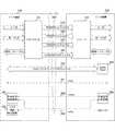
図1は、HDMI規格によるインターフェースの概念構成図である。HDMI規格では、基本となる高速伝送ラインによる伝送方向を一方向に定めており、送信側の機器をソース機器、受信側の機器をシンク機器と呼んでいる。この例では、ソース機器100およびシンク機器200がHDMIケーブル300により接続されている。そして、ソース機器100には送信動作を行うトランスミッタ101が含まれ、シンク機器200には受信動作を行うレシーバ201が含まれている。<1. First embodiment>
[Interface according to HDMI standard]
FIG. 1 is a conceptual block diagram of an interface according to the HDMI standard. In the HDMI standard, the transmission direction of the basic high-speed transmission line is defined in one direction, and the device on the transmission side is called a source device, and the device on the reception side is called a sink device. In this example, the
トランスミッタ101とレシーバ201との間の伝送には、TMDS(Transition Minimized Differential Signaling)と呼ばれるシリアル伝送方式が用いられる。HDMI規格では、映像信号および音声信号は3つのTMDSチャンネル310乃至330を用いて伝送される。すなわち、ある垂直同期信号から次の垂直同期信号までの区間の内、水平帰線区間および垂直帰線区間を除いた区間である有効画像区間において、非圧縮の1画面分の画像の画素データに対応する差動信号が、TMDSチャンネル310乃至330により、シンク機器200に向けて一方向に送信される。また、水平帰線区間または垂直帰線区間においては、音声データ、制御データまたはその他の補助データ等に対応する差動信号が、TMDSチャンネル310乃至330により、シンク機器200に向けて一方向に送信される。 For transmission between the
また、HDMI規格では、クロック信号がTMDSクロックチャンネル340により伝送される。TMDSチャンネル310乃至330の各々では、TMDSクロックチャンネル340により伝送される1クロックの間に、10ビット分の画素データを送信することができる。 Also, in the HDMI standard, a clock signal is transmitted by the
また、HDMI規格では、ディスプレイデータチャンネル(DDC:Display Data Channel)350が設けられる。このディスプレイデータチャンネル350は、本来、シンク機器200におけるEDID ROM282に記憶されるE−EDID情報をソース機器100が読み出すために用いられる。E−EDID(Enhanced Extended Display Identification Data)情報とは、シンク機器200がディスプレイ装置である場合に、その機種、解像度、色の特性およびタイミングなどの設定や性能に関する情報を示すものである。このE−EDID情報は、シンク機器200のEDID ROM282に保持される。 In the HDMI standard, a display data channel (DDC: Display Data Channel) 350 is provided. The
さらに、HDMI規格では、CEC(Consumer Electronics Control)ライン361、Utilityライン362およびHPD(Hot Plug Detect)ライン363等が設けられる。CECライン361は、機器制御信号の双方向通信を行うためのラインである。ディスプレイデータチャンネル350が機器間を1対1に接続するのに対して、このCECライン361はHDMIに接続される全機器において共有されて通信を行う。 Furthermore, in the HDMI standard, a Consumer Electronics Control (CEC)
HPDライン363は、HDMIのケーブルによって他の機器と接続されていること(ホットプラグ)を検知するためのラインである。HDMI1.4規格では、Utilityライン362およびHPDライン363を用いて、シンク機器200からソース機器100にオーディオ信号を同相信号として伝送するARC(Audio Return Channel)が定義されている。本発明の実施の形態では、これらUtilityライン362およびHPDライン363を用いて、シンク機器200からソース機器100に高品質オーディオ信号をより高速に伝送するために、オーディオ信号を差動信号として伝送する。 The
IEC(International Electrotechnical Commission:国際電気標準会議)などで規格化が行われているオーディオフォーマットは、1536KHzのフレームレートまで拡張されている。そのデータレートは最大で49.152Mbpsとなる。一方、HDMI1.4規格で定義されているUtilityライン362およびHPDライン363によるHECチャンネルは、100Base−T信号の伝送に対応しており、その伝送スピードは125Mbpsとなっている。したがって、この伝送路を使用することにより、現在想定されているオーディオの最大データレートの伝送は可能である。 The audio format standardized by IEC (International Electrotechnical Commission: International Electrotechnical Commission) or the like is extended to a frame rate of 1536 KHz. The data rate is up to 49.152 Mbps. On the other hand, the HEC channel by the
図2は、HDMI規格によるコネクタのピン配置例を示す図である。ここでは、タイプAと呼ばれるピン配置におけるピン番号301と信号名称302との対応関係が示されている。 FIG. 2 is a diagram showing an example of pin arrangement of a connector according to the HDMI standard. Here, the correspondence between
TMDSチャンネル310乃至330およびTMDSクロックチャンネル340は、それぞれ正極、シールドおよび負極の3ピンから構成されており、1乃至3番ピンがTMDSチャンネル330、4乃至6番ピンがTMDSチャンネル320、7乃至9番ピンがTMDSチャンネル310、10乃至12番ピンがTMDSクロックチャンネル340にそれぞれ対応している。 The
また、13番ピンがCECライン361に、14番ピンがUtilityライン362に、19番ピンがHPDライン363に、それぞれ対応している。また、ディスプレイデータチャンネル350は、シリアルクロック(SCL)、シリアルデータ(SDA)および接地(グランド)の3ピンから構成されており、15乃至17番ピンがそれぞれ対応する。なお、ディスプレイデータチャンネル350の接地(17番ピン)は、CECライン361の接地と共通化されている。18番ピンは電源供給ライン(+5V)に対応する。 The 13th pin corresponds to the
[ソース機器とシンク機器]
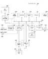
図3は、本発明の実施の形態におけるソース機器100およびシンク機器200の内部構成例について示す図である。ここでは、本技術の実施の形態における要部であるUtilityライン362およびHPDライン363に関する構成を示している。ソース機器100は、シンク機種検出回路110と、プラグ接続検出回路120と、ソース側受信回路140と、同相信号受信回路160と、差動信号受信回路170とを備えている。また、シンク機器200は、ソース機種検出回路210と、プラグ接続伝達回路220と、シンク側送信回路250と、同相信号送信回路260と、差動信号送信回路270とを備えている。[Source device and sink device]
FIG. 3 is a view showing an example of the internal configuration of the
Utilityライン362は、HDMI1.4規格から用いられるようになったラインである。ソース機器100におけるシンク機種検出回路110では、Utilityライン362を介してシンク機器200の機種を検出する。また、シンク機器200におけるソース機種検出回路210では、Utilityライン362を介してソース機器100の機種を検出する。ここにいう機種としては、例えば、HDMI1.4規格のようにUtilityライン362およびHPDライン363によりARCを伝送するようにした機種(以下、ARC対応機種という。)を想定することができる。 The
HPDライン363は、上述のとおりHDMIのケーブルによって他の機器と接続されていることを検知するためのラインである。シンク機器200におけるプラグ接続伝達回路220は、HPDライン363に接続する端子を所定の電圧にバイアスすることにより、シンク機器200が接続されている旨を伝達する。ソース機器100におけるプラグ接続検出回路120は、HPDライン363に接続する端子の電位を基準電位と比較することにより、シンク機器200の接続を検出する。 The
このような機能を有するUtilityライン362およびHPDライン363に対して、本技術の実施の形態では、ソース側受信回路140およびシンク側送信回路250を接続する。すなわち、ソース機器100におけるソース側受信回路140は、コンデンサ131および132と抵抗133とを介してUtilityライン362およびHPDライン363に接続する。また、シンク機器200におけるシンク側送信回路250は、コンデンサ231および232と抵抗233とを介してUtilityライン362およびHPDライン363に接続する。 In the embodiment of the present technology, the source
ソース側受信回路140は、Utilityライン362およびHPDライン363を用いてシンク機器200から伝送される同相信号を同相信号受信回路160に接続し、差動信号を差動信号受信回路170に接続する。 The source
シンク側送信回路250は、Utilityライン362およびHPDライン363を用いてソース機器100に伝送される同相信号を同相信号送信回路260に接続し、差動信号を差動信号送信回路270に接続する。 The sink
なお、本実施の形態において、シンク側送信回路250とソース側受信回路140における差動信号の伝送はAC結合により行われることが望ましい。 In the present embodiment, it is desirable that transmission of differential signals in the sink-
同相信号受信回路160および同相信号送信回路260は、SPDIF規格に準拠した単一方向通信を行うものである。ここで、SPDIF規格とは、デジタルオーディオ信号をリアルタイムに伝送するためのインターフェース規格であり、IECにおいて「IEC 60958」として規格化されている。このSPDIF規格において伝送されるSPDIF信号は、バイフェーズマーク変調されるため、その信号中にクロック成分を含んでいる。なお、これら同相信号受信回路160および同相信号送信回路260は、従来技術により実現される。 The in-phase
差動信号受信回路170および差動信号送信回路270は、本実施の形態において、オーディオ信号の単一方向通信を行うものである。この差動信号についても、データとそれに同期するクロックが伝送される。伝送時の変調としては、MLT−3方式やNRZ方式などが想定される。 The differential
MLT−3方式は、3段階の電圧レベルにより伝送を行うものであり、データが「0」の場合には変化せず、データが「1」の場合に変化する符号として定義される。HDMI1.4規格のHECチャンネルではこのMLT−3方式が採用されており、同様の物理層をオーディオ伝送に必要な周波数で駆動することにより本実施の形態における差動信号を伝送することができる。また、MLT−3方式を利用した場合には、伝送データからクロックを抽出することができる。100Base−Tと同様に、DCフリー化をするために、オーディオ信号に対してマンチェスター符号化を施してもよい。 The MLT-3 system performs transmission at three voltage levels, and is defined as a code that does not change when data is "0" but changes when data is "1". This MLT-3 system is adopted in the HEC channel of the HDMI 1.4 standard, and the differential signal in this embodiment can be transmitted by driving the same physical layer at a frequency necessary for audio transmission. When the MLT-3 method is used, a clock can be extracted from transmission data. Similar to 100Base-T, Manchester encoding may be performed on the audio signal to make it DC free.
NRZ方式は、ビット転送毎に電位をゼロに戻さない方式であり、データが「0」の場合にゼロ電位、データが「1」の場合にプラス電位となる。シンプルな方式であるが、DCフリー化およびクロック情報をデータに埋め込むために、8B10B等のコーディングが必要となる。8B10Bは、8ビットのデータにクロックを埋め込んで10ビットのデータに変換して転送する方式である。 The NRZ method is a method in which the potential is not returned to zero every bit transfer, and becomes zero potential when data is “0” and plus potential when data is “1”. Although this is a simple method, coding such as 8B10B is required to make DC free and embed clock information into data. In 8B10B, a clock is embedded in 8-bit data to convert it into 10-bit data and transfer it.
なお、同相信号受信回路160は、特許請求の範囲に記載の第2の受信部の一例である。また、差動信号受信回路170は、特許請求の範囲に記載の第1の受信部の一例である。また、同相信号送信回路260は、特許請求の範囲に記載の第2の送信部の一例である。また、差動信号送信回路270は、特許請求の範囲に記載の第1の送信部の一例である。また、プラグ接続検出回路120は、特許請求の範囲に記載の状態受領部の一例である。また、プラグ接続伝達回路220は、特許請求の範囲に記載の状態通知部の一例である。 The in-phase
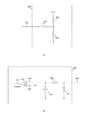
図4は、本技術の実施の形態におけるソース側受信回路140およびシンク側送信回路250の一構成例を示す図である。 FIG. 4 is a diagram showing a configuration example of the source
図4におけるaに示すように、シンク側送信回路250は、増幅器251と、加算器252および253とを備えている。 As shown in a of FIG. 4, the sink-
増幅器251は、差動信号送信回路270から供給される信号を増幅する増幅器である。この増幅器251の出力は差動信号になっており、加算器252には正極の信号が、加算器253には負極の信号がそれぞれ供給される。 The
加算器252は、同相信号送信回路260から供給される信号と増幅器251の正極出力とを加算する回路である。加算器253は、同相信号送信回路260から供給される信号と増幅器251の負極出力とを加算する回路である。 The
すなわち、増幅器251から出力される信号が差動信号であるのに対して、加算器252および253により重畳される信号は同相信号である。これにより、両信号は、同じ一対の信号線(Utilityライン362およびHPDライン363)によって伝送することが可能となる。 That is, while the signal output from the
図4におけるbに示すように、ソース側受信回路140は、増幅器141と、加算器142とを備えている。 As shown by b in FIG. 4, the source
増幅器141は、Utilityライン362およびHPDライン363からの信号を増幅する増幅器である。Utilityライン362およびHPDライン363の信号は差動信号になっており、増幅器141は差動入力により動作する。 The
加算器142は、増幅器141の出力の正極の信号と負極の信号とを加算する回路である。 The
すなわち、Utilityライン362およびHPDライン363によって伝送された信号のうち、差動信号が増幅器141によって抽出され、同相信号が加算器142によって抽出される。 That is, among the signals transmitted by the
図5は、本技術の実施の形態における動作の概要を示す図である。上述のように、14番ピンはUtilityライン362に対応し、19番ピンはHPDライン363に対応する。HDMI1.4規格以前の機器では、Utilityライン362およびHPDライン363によって同相信号または差動信号の何れも伝送されない。HDMI1.4規格のように同相信号が伝送される場合には、14番ピンおよび19番ピンに正極信号が重畳される。本実施の形態のように差動信号が伝送される場合には、14番ピンに正極信号が重畳され、19番ピンに負極信号が重畳される。本実施の形態では、同相信号および差動信号を同時に伝送することも可能である。 FIG. 5 is a diagram showing an outline of an operation in the embodiment of the present technology. As described above, the 14th pin corresponds to the
したがって、同相信号および差動信号は、Utilityライン362およびHPDライン363において互いに独立して伝送することができ、両信号を伝送する場合や一方の信号のみを伝送する場合でも、受信側(ソース側受信回路140)に特別な機構を要することなく対応することができる。 Therefore, the in-phase signal and the differential signal can be transmitted independently on the
シンク機器200側からの高品質オーディオ伝送がユーザによって所望された場合、ソース機器100またはシンク機器200は、CECライン361等によるコマンドや、DDC350による通信を用いて、その伝送機能のアクティベートを要求する。例えば、ユーザがシンク機器200としてのディスプレイのリモートコントローラを用いてその機能を選択した場合や、ソース機器100としてのオーディオ再生機を起動することによってその伝送機能を選択した場合が、これに該当する。アクティベート要求を受けたソース機器100またはシンク機器200は、自身がその伝送機能に対応しているか否かを、現在のTMDSチャンネルの使用状況等を鑑みて、そのアクティベート要求への回答として同様の方法で送信する。アクティベーション要求への回答を受領次第、または、回答を送信し次第、双方のデバイスとも構成を変更して、高品質オーディオ伝送を開始する。同様に、その伝送機能を中止または停止する際にも、同様のコマンド等のやり取りを行うことにより、実現することができる。 When high-quality audio transmission from the
[機種検出]
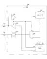
図6は、本技術の実施の形態におけるシンク機種検出回路110およびソース機種検出回路210の構成例を示す図である。[Model detection]
FIG. 6 is a diagram showing a configuration example of the sink
図6におけるaに示すように、シンク機種検出回路110は、抵抗111および112と、コンデンサ113と、比較器116とを備えている。抵抗111は、Utilityライン362を+5Vにプルアップするものである。この抵抗111は、ソース機器100が特定の機種である場合のみ存在し、ソース機器100が特定の機種でない場合にはプルアップが行われない。抵抗112およびコンデンサ113は、ローパスフィルタを構成するものである。このローパスフィルタの出力は信号線114に供給される。比較器116は、ローパスフィルタから信号線114に供給された直流電位を、信号線115に与えられた基準電位と比較するものである。 As shown in a of FIG. 6, the sink
また、図6におけるbに示すように、ソース機種検出回路210は、抵抗211および212と、コンデンサ213と、比較器216とを備えている。抵抗211は、Utilityライン362を接地電位にプルダウンするものである。この抵抗211は、シンク機器200が特定の機種である場合のみ存在し、シンク機器200が特定の機種でない場合にはプルダウンが行われない。抵抗212およびコンデンサ213は、ローパスフィルタを構成するものである。このローパスフィルタの出力は信号線215に供給される。比較器216は、ローパスフィルタから信号線215に供給された直流電位を、信号線214に与えられた基準電位と比較するものである。 Further, as shown by b in FIG. 6, the source
シンク機器200が特定の機種であれば抵抗211によるプルダウンが行われてUtilityライン362の電位が2.5Vとなり、シンク機器200が特定の機種でなければ開放されて5Vとなる。したがって、信号線115の基準電位を例えば3.75Vとすれば、信号線117の出力に基づいて、ソース機器100においてシンク機器200の機種を識別することができる。 If the
同様に、ソース機器100が特定の機種であれば抵抗111によるプルアップが行われてUtilityライン362の電位が2.5Vとなり、ソース機器100が特定の機種でなければ0Vとなる。したがって、信号線214の基準電位を例えば1.25Vとすれば、信号線217の出力に基づいて、シンク機器200においてソース機器100の機種を識別することができる。 Similarly, if the
これら機種検出のための信号は直流バイアス電位で伝達されるため、交流信号として伝達される同相信号および差動信号に影響を与えるものではない。 Since the signals for detecting these types of devices are transmitted at a DC bias potential, they do not affect the in-phase signal and the differential signal transmitted as an AC signal.
[接続検出]
図7は、本技術の実施の形態におけるプラグ接続検出回路120およびプラグ接続伝達回路220の構成例を示す図である。Connection Detection
FIG. 7 is a diagram showing a configuration example of the plug
図7におけるaに示すように、プラグ接続伝達回路220は、チョークコイル221と、抵抗222および223とを備えている。これらチョークコイル221、抵抗222および223は、HPDライン363を例えば約4Vにバイアスするものである。 As shown in a of FIG. 7, the plug
また、図7におけるbに示すように、プラグ接続検出回路120は、抵抗121および122と、コンデンサ123と、比較器126とを備えている。抵抗121は、HPDライン363を接地電位にプルダウンするものである。抵抗122およびコンデンサ123は、ローパスフィルタを構成するものである。このローパスフィルタの出力は信号線124に供給される。比較器126は、ローパスフィルタから信号線124に供給された直流電位を、信号線125に与えられた基準電位と比較するものである。 Further, as shown by b in FIG. 7, the plug
ここで、信号線125に基準電位として例えば1.4Vを与えるものとする。ソース機器100がHPDライン363に接続されていなければ、入力電位は抵抗121によるプルダウンされることにより信号線124の電位は信号線125の基準電位よりも低くなる。一方、ソース機器100がHPDライン363に接続されていれば、約4Vにバイアスされるため、信号線124の電位は信号線125の基準電位よりも高くなる。したがって、信号線127の出力に基づいて、ソース機器100においてシンク機器200の接続の有無を検出することができる。 Here, for example, 1.4 V is applied to the
これらプラグ接続検出のための信号は直流バイアス電位で伝達されるため、交流信号として伝達される同相信号および差動信号に影響を与えるものではない。 Since signals for detecting these plug connections are transmitted at a DC bias potential, they do not affect the in-phase signal and the differential signal transmitted as an AC signal.
このように、本技術の第1の実施の形態によれば、TMDSチャンネルとは独立した高品位オーディオ伝送路を形成することが可能になる。上述の実施の形態では、その伝送方向としてARCのようにTMDSチャンネルとは逆方向を想定したが、TMDSチャンネルと順方向にしてもよい。逆方向の場合は高品質オーディオ伝送に対応したARCアプリケーションを実現することができ、順方向の場合はビデオ伝送を必要としないオーディオ専用伝送アプリケーションを実現することができる。 Thus, according to the first embodiment of the present technology, it is possible to form a high definition audio transmission path independent of the TMDS channel. In the above embodiment, the transmission direction is assumed to be the reverse direction to the TMDS channel like ARC, but may be the forward direction to the TMDS channel. In the reverse direction, an ARC application compatible with high quality audio transmission can be realized, and in the forward direction, an audio only transmission application not requiring video transmission can be realized.
<2.第2の実施の形態>
上述の第1の実施の形態において高品質オーディオ伝送が可能になると、その伝送において著作権保護が必要になる場合がある。この第2の実施の形態では、著作権保護のために必要となる認証および鍵交換の手法について説明する。<2. Second embodiment>
If high quality audio transmission is enabled in the first embodiment described above, copyright protection may be required in the transmission. In the second embodiment, an authentication and key exchange method required for copyright protection will be described.
図8は、一般的な高品位コンテンツ伝送における著作権保護技術適用システムの概要を示す図である。この著作権保護技術適用システムでは、オーディオ信号を送信する送信機10と、そのオーディオ信号を受信する受信機20とを備える。 FIG. 8 is a diagram showing an outline of a copyright protection technology application system in general high-definition content transmission. This copyright protection technology application system includes a
送信機10は、送信部11と、暗号化部12と、通信部13と、認証/鍵交換部14とを備える。通信部13は、オーディオ信号の暗号化に必要な鍵交換や機器の認証のための通信を行うものである。認証/鍵交換部14は、通信部13を介して機器の認証や、鍵交換を行うものである。暗号化部12は、認証/鍵交換部14から供給された暗号鍵を用いてオーディオ信号を暗号化するものである。送信部11は、暗号化部12によって暗号化されたオーディオ信号を送信するものである。 The
受信機20は、受信部21と、復号化部22と、通信部23と、認証/鍵交換部24とを備えている。受信部21は、送信機10から送信された暗号化オーディオ信号を受信するものである。復号化部22は、受信部21によって受信された暗号化オーディオ信号を復号するものである。通信部23は、オーディオ信号の復号に必要な鍵交換や機器の認証のための通信を行うものである。認証/鍵交換部24は、通信部23を介して機器の認証や、鍵交換を行うものである。 The
すなわち、送信機10および受信機20は、暗号化オーディオ信号を伝送する伝送路とは別に、機器認証および鍵交換のための双方向通信チャンネルを有する。認証/鍵交換手順としては、例えばRSAの鍵ペアなど機器毎の秘密鍵をベースとした機器認証を行う。その通信過程において、双方が共有する乱数によってコンテンツ鍵を暗号化して送信機10から受信機20に送信することにより、送信機10および受信機20の双方において同じコンテンツ鍵を共有する。そして、そのコンテンツ鍵を用いて、例えばAESなどの暗号器および復号器によって、コンテンツ情報を送信機10では暗号化、受信機20では復号化することにより、安全に伝送する。なお、コンテンツ鍵は、その安全性をさらに高めるために、一定間隔で更新するようにしてもよい。 That is, the
なお、通信部13または通信部23は、特許請求の範囲に記載の通信部の一例である。 The
本技術の第2の実施の形態においては、上述の著作権保護のための通信路は以下のように実現することが考えられる。第1の実施例としては、HDMI規格のDDC350を利用することが考えられる。本技術の実施の形態による高品質オーディオ信号が伝送されている期間には、TMDSチャンネルによって映像信号の伝送は行われない。したがって、DDC350を本伝送の著作権保護情報通信に使ってもよい。TMDSチャンネルの伝送方向と順方向に通信する場合には、HDMI規格の通りでそのまま適用可能である。TMDSチャンネルの伝送方向と逆方向に通信する場合には、HDMI規格のDDC350による通信を逆方向で構成する必要がある。そこで、本技術の第2の実施の形態においては、後述するように、通常はシンク機器200側に実装されるDDCレジスタをソース機器100側にも実装し、シンク機器200をマスターとして動作させる。 In the second embodiment of the present technology, it is conceivable that the above-mentioned communication path for copyright protection is realized as follows. As a first embodiment, it is conceivable to use
第2の実施例としては、Utilityライン362およびHPDライン363に同相信号として重畳して通信する方法が考えられる。認証に必要なデータ伝送は、双方向で高々数100Kbps程度であるため、同相信号として重畳しても差動信号の品質を保つことが可能である。この第2の実施例によれば、DDC350における変更は不要となる。 As a second embodiment, a method may be considered in which the
以下では、著作権保護のための通信路の第1の実施例としてDDC350を双方向ラインに変更する例について説明する。図2により説明したように、DDC350は、シリアルクロック(SCL)、シリアルデータ(SDA)および接地(グランド)の3ピンから構成される。シンク機器200にはEDID ROM282などのレジスタ群が設けられ、SCLラインのタイミングに基づいてレジスタ群がアクセスされるとともに、SDAラインがドライブされる。 In the following, an example of changing the
[双方向DDC]
図9は、本技術の第2の実施の形態におけるソース機器100の構成例を示す図である。図10は、本技術の第2の実施の形態におけるシンク機器200の構成例を示す図である。ここでは、ソース機器100およびシンク機器200が、SCLライン351およびSDAライン352により接続される様子を示している。なお、ここでは、グランドラインを省略している。[Bidirectional DDC]
FIG. 9 is a diagram illustrating a configuration example of the
ソース機器100は、処理部181と、DDCレジスタ183と、セレクタ184と、ドライバ185乃至187とを備えている。同様に、シンク機器200は、処理部281と、DDCレジスタ283と、セレクタ284と、ドライバ285乃至287とを備えている。 The
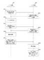
ソース機器100からシンク機器200にデータ伝送する場合、ソース機器100がマスターとなり、処理部181から伝送方向信号DIRとして「1」が出力される。これにより、ドライバ185が動作し、ドライバ186の出力がハイインピーダンスとなる。そのため、処理部181からのクロック信号CLKがSCLライン351に出力される。また、セレクタ184は、処理部181からのデータ信号DATAを選択する。そのため、ドライバ187を介してデータ信号DATAがSDAライン352に出力される。 When data is transmitted from the
この場合において、シンク機器200はスレーブとなり、処理部281から伝送方向信号DIRとして「0」が出力される。これにより、ドライバ286が動作し、ドライバ285の出力がハイインピーダンスとなる。そのため、SCLライン351の値がクロック信号CKとしてDDCレジスタ283に入力される。また、セレクタ284は、SDAライン352の値をデータ信号DとしてDDCレジスタ283に接続される。そのため、DDCレジスタ283は、クロック信号CKに従って、データ信号Dを保持または出力する。 In this case, the
一方、シンク機器200からソース機器100にデータ伝送する場合、シンク機器200がマスターとなり、処理部281から伝送方向信号DIRとして「1」が出力される。また、この場合、ソース機器100がスレーブとなり、処理部181から伝送方向信号DIRとして「0」が出力される。すなわち、ソース機器100およびシンク機器200が上述の場合とは逆の動作を行う。なお、この伝送方向の切り替えにあたっては、上述のようにソース機器100およびシンク機器200の双方において構成の変更が周知されている必要がある。 On the other hand, when data is transmitted from the
このようにして、DDC350が双方向化されることにより、ソース機器100およびシンク機器200の間において、著作権保護に必要な情報のやりとりが可能となる。 In this manner, by making the
[認証および鍵交換の手順]
図11は、本技術の第2の実施の形態における認証および鍵交換の手順の一例を示すシーケンス図である。[Authentication and key exchange procedure]
FIG. 11 is a sequence diagram illustrating an example of an authentication and key exchange procedure according to the second embodiment of the present technology.
まず、ソース機器100は、認証局による証明書が付与されたソース機器100の公開鍵をシンク機器200に対して送信する(S911)。ソース機器100の公開鍵を受信したシンク機器200は、認証局による証明書が付与されたシンク機器200の公開鍵およびデバイスIDをソース機器100に対して送信する(S921)。 First, the
シンク機器200の公開鍵およびデバイスIDを受信したソース機器100は、デバイスIDを参照して無効デバイスに該当しない旨を確認する(S913)。無効デバイスに該当する場合には処理を中止する。無効デバイスに該当しない場合には、ソース機器100は、乱数を発生して、その乱数をシンク機器200の公開鍵によって暗号化して、シンク機器200に送信する(S914)。 The
シンク機器200は、乱数を発生して、その乱数をソース機器100の公開鍵によって暗号化する。そして、シンク機器200は、ソース機器100から受信した暗号化データおよび自身で暗号化した暗号化データの両者を署名して、自身で暗号化した暗号化データと署名データとをソース機器100に送信する(S925)。 The
ソース機器100は、シンク機器200から受信した署名データを検証する(S916)。ここで、署名が正しくない場合には処理を中止する。署名が正しければ、シンク機器200から受信した暗号化データおよび自身で暗号化した暗号化データの両者を署名してシンク機器200に送信する。そして、ソース機器100自身が送信した乱数とシンク機器200から受信した暗号化データを復号したデータとから鍵を生成する(S917)。 The
シンク機器200は、ソース機器100から受信した署名データを検証する(S928)。ここで、署名が正しくない場合には処理を中止する。署名が正しければ、シンク機器200自身が送信した乱数とソース機器100から受信した暗号化データを復号したデータとから鍵を生成する(S929)。 The
このようにしてソース機器100およびシンク機器200の双方において生成された鍵は、オーディオ信号の暗号化および復号に用いられる。 The keys thus generated in both the
このように、本技術の第2の実施の形態によれば、著作権保護を施した状態で、高品質オーディオ伝送を実現することができる。 Thus, according to the second embodiment of the present technology, high quality audio transmission can be realized with copyright protection.
<3.第3の実施の形態>
上述の第1の実施の形態では、Utilityライン362およびHPDライン363を用いて、シンク機器200からソース機器100にクロック成分を含むオーディオ信号を差動信号として伝送していた。これに対し、この第3の実施の形態では、オーディオ信号を差動信号として伝送する一方で、オーディオ信号のクロック信号を同相信号として伝送する。なお、基本的な構成は第1の実施の形態と同様であるため、詳細な説明は省略する。<3. Third embodiment>
In the first embodiment described above, an audio signal including a clock component is transmitted as a differential signal from the
この第3の実施の形態において、クロック信号は、オーディオ信号のワードクロックを用いることができる。また、ワードクロックが高速となってしまう場合には、その基本クロックを用いてもよい。基本クロックの周波数としては、例えば、32KHz、44.1KHzまたは48KHzなどが想定される。基本クロックを用いた場合、実際のワードクロックはこれらの倍数となる。ただし、不要輻射を抑えるために、十分低速な信号となることが望ましい。 In the third embodiment, a clock signal can be a word clock of an audio signal. In addition, when the word clock becomes fast, the basic clock may be used. As the frequency of the basic clock, for example, 32 KHz, 44.1 KHz or 48 KHz etc. are assumed. When a basic clock is used, the actual word clock is a multiple of these. However, in order to suppress unwanted radiation, it is desirable that the signal be sufficiently slow.
この同相信号によるクロック信号は、オーディオ信号と同じ方向で伝送することにより、受信側で再生クロックを容易に生成することが可能になる。なお、この同相信号によるクロック信号を受信側から逆方向で伝送することにより、受信側のマスタークロックに同期した高品質再生用クロックとすることも考えられる。 By transmitting the clock signal by the in-phase signal in the same direction as the audio signal, it is possible to easily generate a reproduction clock on the receiving side. By transmitting a clock signal based on the in-phase signal in the reverse direction from the receiving side, it is also conceivable to set a high quality reproduction clock synchronized with the master clock on the receiving side.
<4.適用例>
上述の実施の形態では、HDMI規格に準じたインターフェース回路への適用例について説明したが、本技術は他の構成においても適用可能である。ここではその適用例として、ディスクプレイヤ、テレビ受信機およびデジタルカメラの適用例について説明する。<4. Application example>
Although the above-mentioned embodiment explained the example of application to the interface circuit based on HDMI standard, this art is applicable also in other composition. Here, as an application example, an application example of a disc player, a television receiver and a digital camera will be described.
図12は、本技術の実施の形態におけるディスクプレイヤ500の構成例を示す図である。このディスクプレイヤ500は、プロセッサ511と、フラッシュROM512と、SDRAM513と、表示制御部514とを備える。また、このディスクプレイヤ500は、SATAインターフェース521と、BDドライブ522と、イーサネット(登録商標)インターフェース523と、ネットワーク端子524とを備える。また、このディスクプレイヤ500は、高速バスインターフェース525と、HDMI送信部526と、HDMI端子527と、リモコン受信部529とを備える。また、このディスクプレイヤ500は、MPEGデコーダ533と、映像出力端子538と、音声出力端子539とを備える。また、このディスクプレイヤ500は、グラフィック生成回路542と、パネル駆動回路543と、表示パネル544とを備える。プロセッサ511、フラッシュROM512、SDRAM513、表示制御部514、SATAインターフェース521、イーサネットインターフェース523、MPEGデコーダ533は、バス510によって相互に接続される。 FIG. 12 is a diagram illustrating a configuration example of the disc player 500 according to the embodiment of the present technology. The disc player 500 includes a
プロセッサ511は、ディスクプレイヤ500の全体を制御するものである。フラッシュROM512は、プロセッサ511の動作に必要なプログラム等を記憶するメモリである。SDRAM513は、プロセッサ511の動作に必要なデータ等を記憶するメモリである。 The
SATAインターフェース521は、シリアルATAを接続するためのインターフェースである。BDドライブ522は、ブルーレイディスク(Blu-ray(登録商標)Disc)を駆動するためのディスクドライブである。イーサネットインターフェース523は、イーサネットを接続するためのインターフェースである。ネットワーク端子524は、イーサネットを接続するための端子である。 The
高速バスインターフェース525は、HDMI規格のUtilityライン362およびHPDライン363である。HDMI送信部526は、HDMI規格のインターフェースに対する送信回路である。HDMI端子527は、HDMI規格に整合する端子である。 The high-
リモコン受信部529は、ユーザの操作する(図示しない)リモコンからの信号を受信するものである。 The remote
MPEGデコーダ533は、MPEG規格に準ずる信号を復号するデコーダである。映像出力端子538は、映像信号を出力する端子である。音声出力端子539は、音声信号を出力する端子である。 The
表示制御部514は、表示パネル544における表示に必要な制御を行うものである。グラフィック生成回路542は、表示パネル544に表示するためのグラフィック画像を生成するものである。パネル駆動回路543は、表示パネル544を駆動するための回路である。表示パネル544は、映像を表示するパネルである。ここでは、表示パネル544を内蔵するディスクプレイヤ500を想定したが、表示パネル544を内蔵しないものも考えられる。 The
高速バスインターフェース525は、イーサネットインターフェース523とHDMI端子527との間に挿入される。この高速バスインターフェース525は、プロセッサ511から供給される送信データを、HDMI端子527からHDMIケーブルを介して相手側の機器に送信する。また、この高速バスインターフェース525は、HDMIケーブルからHDMI端子527を介して相手側の機器から受信された受信データをプロセッサ511に供給する。 The high-
コンテンツ記録時には、(図示しない)デジタルチューナを介して、イーサネットインターフェース523を介して、または、高速バスインターフェース525を介して、記録すべきコンテンツデータが取得される。このコンテンツデータは、SATAインターフェース521に入力され、BDドライブ522によってBDに記録される。このコンテンツデータは、SATAインターフェース521に接続された、(図示しない)HDD(ハードディスクドライブ)に記録されてもよい。 At the time of content recording, content data to be recorded is acquired via a digital tuner (not shown), via the
コンテンツ再生時には、BDドライブ522によりBDから再生されたコンテンツデータ(MPEGストリーム)は、SATAインターフェース521を介してMPEGデコーダ533に供給される。MPEGデコーダ533では、再生されたコンテンツデータに対してデコード処理が行われ、ベースバンドの画像および音声のデータが得られる。画像データは、グラフィック生成回路542を通じて映像出力端子538に出力される。また、音声データは、音声出力端子539に出力される。 At the time of content reproduction, content data (MPEG stream) reproduced from the BD by the BD drive 522 is supplied to the
また、コンテンツ再生時には、MPEGデコーダ533で得られた画像データが、ユーザ操作に応じて、グラフィック生成回路542を通じてパネル駆動回路543に供給され、表示パネル544に再生画像が表示される。また、MPEGデコーダ533で得られた音声データが、ユーザ操作に応じて、(図示しない)スピーカに供給され、再生画像に対応した音声が出力される。 Further, at the time of content reproduction, the image data obtained by the
また、このコンテンツ再生時に、MPEGデコーダ533で得られた画像および音声のデータをHDMIのTMDSチャンネルで送信する場合には、これら画像および音声のデータは、HDMI送信部526に供給されてパッキングされる。そして、このHDMI送信部526からHDMI端子527に、画像および音声のデータが出力される。 In addition, when the image and audio data obtained by the
また、コンテンツ再生時に、BDドライブ522で再生されたコンテンツデータをネットワークに送出する際には、このコンテンツデータは、イーサネットインターフェース523を介して、ネットワーク端子524に出力される。同様に、コンテンツ再生時に、BDドライブ522で再生されたコンテンツデータをHDMIケーブルの双方向通信路に送出する際には、そのコンテンツデータは、高速バスインターフェース525を介して、HDMI端子527に出力される。ここで、画像データを出力する前に、著作権保護技術、例えばHDCP、DTCP、DTCP+などを用いて暗号化してから伝送してもよい。 Further, when content data reproduced by the BD drive 522 is transmitted to the network at the time of content reproduction, the content data is output to the
図13は、本技術の実施の形態におけるテレビ受信機600の構成例を示す図である。このテレビ受信機600は、プロセッサ611と、フラッシュROM612と、SDRAM613と、表示制御部614とを備える。また、このテレビ受信機600は、イーサネットインターフェース623と、ネットワーク端子624とを備える。また、このテレビ受信機600は、高速バスインターフェース625と、HDMI受信部626と、HDMI端子627と、リモコン受信部629とを備える。また、このテレビ受信機600は、アンテナ端子631と、デジタルチューナ632と、MPEGデコーダ633とを備える。また、このテレビ受信機600は、映像信号処理回路641と、グラフィック生成回路642と、パネル駆動回路643と、表示パネル644とを備える。また、このテレビ受信機600は、音声信号処理回路651と、音声増幅回路653と、スピーカ654とを備える。プロセッサ611、フラッシュROM612、SDRAM613、表示制御部614、イーサネットインターフェース623、高速バスインターフェース625、および、MPEGデコーダ633は、バス610によって相互に接続される。 FIG. 13 is a diagram showing a configuration example of the
プロセッサ611は、テレビ受信機600の全体を制御するものである。フラッシュROM612は、プロセッサ611の動作に必要なプログラム等を記憶するメモリである。SDRAM613は、プロセッサ611の動作に必要なデータ等を記憶するメモリである。表示制御部614は、表示パネル644における表示に必要な制御を行うものである。 The
イーサネットインターフェース623は、イーサネットを接続するためのインターフェースである。ネットワーク端子624は、イーサネットを接続するための端子である。高速バスインターフェース625は、HDMI規格のUtilityライン362およびHPDライン363である。HDMI受信部626は、HDMI規格のインターフェースに対する送信回路である。HDMI端子627は、HDMI規格に整合する端子である。 The
リモコン受信部629は、ユーザの操作する(図示しない)リモコンからの信号を受信するものである。 The remote
アンテナ端子631は、(図示しない)受信アンテナによって受信されたテレビ放送信号を入力する端子である。デジタルチューナ632は、アンテナ端子631に入力されたテレビ放送信号を処理して、ユーザの選択チャネルに対応した所定のトランスポートストリームから、パーシャルTSを抽出するものである。 The
MPEGデコーダ633は、MPEG規格に準ずる信号を復号するデコーダである。MPEGデコーダ633は、デジタルチューナ632において得られる映像データのTSパケットにより構成される映像PESパケットに対してデコード処理を行って画像データを得る。また、MPEGデコーダ633は、デジタルチューナ632で得られる音声データのTSパケットにより構成される音声PESパケットに対してデコード処理を行って音声データを得る。 The
映像信号処理回路641およびグラフィック生成回路642は、MPEGデコーダ633において得られた画像データ、または、HDMI受信部626において受信された画像データに対して必要に応じて信号処理を行うものである。この信号処理としては、例えば、スケーリング処理(解像度変換処理)、グラフィックスデータの重畳処理、WCG画像のガンマ補正等が想定される。パネル駆動回路643は、グラフィック生成回路642から出力される映像(画像)データに基づいて、表示パネル644を駆動するための回路である。表示パネル644は、映像を表示するパネルである。この表示パネル644は、例えば、LCD(Liquid Crystal Display)、PDP(Plasma Display Panel)、有機EL(Organic Electro-Luminescence)パネル等によって構成され得る。 The video
なお、この実施の形態では、プロセッサ611の他に表示制御部614を有する例を示しているが、表示パネル644における表示をプロセッサ611が直接制御するようにしてもよい。また、プロセッサ611と表示制御部614は、1つのチップにより構成されてもよく、また、複数コアであってもよい。 In this embodiment, an example in which the
音声信号処理回路651は、MPEGデコーダ633において得られた音声データに対してD/A変換等の必要な処理を行うものである。音声増幅回路653は、音声信号処理回路651から出力される音声信号を増幅してスピーカ654に供給するものである。なお、スピーカ654は、モノラルでもステレオでもよい。また、スピーカ654は、1つでもよく、2つ以上でもよい。また、スピーカ654は、イヤホン、ヘッドホンでもよい。また、スピーカ654は、2.1チャネルや、5.1チャネルなどに対応するものであってもよい。また、スピーカ654は、テレビ受信機600と無線で接続してもよい。また、スピーカ654は、他機器であってもよい。 The audio
アンテナ端子631に入力されたテレビ放送信号は、デジタルチューナ632に供給される。このデジタルチューナ632では、テレビ放送信号を処理して、ユーザの選択チャネルに対応した所定のトランスポートストリームが出力される。そして、トランスポートストリームから、パーシャルTS(映像データのTSパケット、音声データのTSパケット)が抽出され、このパーシャルTSはMPEGデコーダ633に供給される。 The television broadcast signal input to the
MPEGデコーダ633では、映像データのTSパケットにより構成される映像PESパケットに対してデコード処理が行われて映像データが得られる。この映像データは、映像信号処理回路641およびグラフィック生成回路642において、必要に応じて、スケーリング処理(解像度変換処理)、グラフィックスデータの重畳処理等が行われた後に、パネル駆動回路643に供給される。そのため、表示パネル644には、ユーザの選択チャネルに対応した画像が表示される。 The
また、MPEGデコーダ633では、音声データのTSパケットにより構成される音声PESパケットに対してデコード処理が行われて音声データが得られる。この音声データは、音声信号処理回路651においてD/A変換等の必要な処理が行われ、さらに、音声増幅回路653で増幅された後に、スピーカ654に供給される。そのため、スピーカ654から、ユーザの選択チャネルに対応した音声が出力される。 Also, in the
また、ネットワーク端子624からイーサネットインターフェース623に供給され、または、HDMI端子627から高速バスインターフェース625を介して供給されるコンテンツデータ(画像データ、音声データ)は、MPEGデコーダ633に供給される。それ以降は、上述のテレビ放送信号の受信時と同様の動作となり、表示パネル644に画像が表示され、スピーカ654から音声が出力される。 Also, content data (image data, audio data) supplied from the
また、HDMI受信部626では、HDMI端子627にHDMIケーブルを介して接続されているディスクプレイヤ500から送信される画像データおよび音声データが取得される。画像データは、映像信号処理回路641に供給される。また、音声データは、直接、音声信号処理回路651に供給される。それ以降は、上述のテレビ放送信号の受信時と同様の動作となり、表示パネル644に画像が表示され、スピーカ654から音声が出力される。 Also, in the
図14は、本技術の実施の形態におけるデジタルカメラ700の構成例を示す図である。このデジタルカメラ700は、システム制御プロセッサ711と、フラッシュROM712と、SDRAM713と、表示制御部714とを備える。また、このデジタルカメラ700は、高速バスインターフェース725と、HDMI送信部726と、HDMI端子727と、ユーザ操作部728とを備える。また、このデジタルカメラ700は、グラフィック生成回路742と、パネル駆動回路743と、表示パネル744とを備える。また、このデジタルカメラ700は、イメージャ751と、イメージャドライバ752と、カメラ制御部753とを備える。また、このデジタルカメラ700は、撮像信号処理回路754と、マイクロフォン755と、音声信号処理回路756と、静止画像信号処理回路757と、動画像信号処理回路758と、記録再生部759と、メモリカード760とを備える。 FIG. 14 is a diagram showing a configuration example of the
システム制御プロセッサ711は、デジタルカメラ700の全体を制御するものである。フラッシュROM712は、システム制御プロセッサ711の動作に必要なプログラム等を記憶するメモリである。SDRAM713は、システム制御プロセッサ711の動作に必要なデータ等を記憶するメモリである。表示制御部714は、表示パネル744における表示に必要な制御を行うものである。 A
高速バスインターフェース725は、HDMI規格のUtilityライン362およびHPDライン363である。HDMI送信部726は、HDMI規格のインターフェースに対する送信回路である。HDMI端子727は、HDMI規格に整合する端子である。 The high-
ユーザ操作部728は、ユーザからの操作を受け付けるものである。このユーザ操作部728は、例えば、スイッチ、ホイール、近接/タッチにより指示入力を行うタッチパネル部、マウス、キーボード、カメラで指示入力を検出するジェスチャ入力部、音声により指示入力を行う音声入力部、さらにはリモートコントロールなどであってもよい。システム制御プロセッサ711は、ユーザ操作部728の操作状態を判断し、デジタルカメラ700の動作を制御する。ユーザは、ユーザ操作部728により、撮像(記録)操作、再生操作の他に、各種付加情報の入力操作等を行うことができる。 The
グラフィック生成回路742は、表示パネル744に表示するためのグラフィック画像を生成するものである。パネル駆動回路743は、表示パネル744を駆動するための回路である。表示パネル744は、映像を表示するパネルである。 The
イメージャ751は、受光した光信号を電気信号に変換する光電変換素子である。イメージャドライバ752は、イメージャ751を駆動するドライバである。カメラ制御部753は、イメージャドライバ752および撮像信号処理回路754を制御するものである。撮像信号処理回路754は、イメージャ751から供給された電気信号を撮像信号として信号処理を行うものである。 The
マイクロフォン755は、周囲の音声を変換して音声信号を生成するものである。
音声信号処理回路756は、マイクロフォン755によって生成された音声信号について信号処理を行うものである。The
The audio
静止画像信号処理回路757は、撮像信号処理回路754から供給された静止画像信号について信号処理を行うものである。動画像信号処理回路758は、撮像信号処理回路754および音声信号処理回路756から供給された動画像信号について信号処理を行うものである。 The still image
記録再生部759は、メモリカード760やフラッシュROM712などにアクセスして、静止画像データまたは動画像データを読み書きするものである。メモリカード760は、静止画像データまたは動画像データを記録する記録媒体である。 The recording and reproducing
イメージャ751において得られた撮像信号は、撮像信号処理回路754に供給されて処理され、この撮像信号処理回路754からは被写体に対応した画像データ(撮像画像データ)が得られる。静止画撮像時には、静止画像信号処理回路757では、撮像信号処理回路754から出力される画像データに対して、圧縮符号化処理等が施されて、静止画像データが生成される。この静止画像データは、記録再生部759により、メモリカード760等に記録される。 The imaging signal obtained by the
また、動画撮像時には、動画像信号処理回路758では、撮像信号処理回路754から出力される画像データに対して、音声信号処理回路756から出力される音声データとともに、記録メディアフォーマットに準じた圧縮符号化等の処理が施され、音声データが付加された動画像データが生成される。この動画像データは、記録再生部759により、メモリカード760等に記録される。 In addition, at the time of moving image capturing, in the moving image
静止画像の再生時には、メモリカード760等から静止画像データが読み出され、静止画像信号処理回路757で復号化等の処理が施されて再生画像データ得られる。この再生画像データはシステム制御プロセッサ711および動画像信号処理回路758を介してパネル駆動回路743に供給され、表示パネル744に、静止画像が表示される。 At the time of reproduction of a still image, still image data is read from the
動画像の再生時には、記録再生部759によりメモリカード760等から動画像データが読み出され、動画像信号処理回路758において復号化等の処理が施されて再生画像データが得られる。そして、再生画像データはパネル駆動回路743に供給され、表示パネル744に、動画像が表示される。 At the time of reproduction of a moving image, moving image data is read from the
メモリカード760等に記録されている静止画像データまたは動画像データに係る画像または音声のデータを外部機器(シンク機器)に送信する場合、メモリカード760から静止画画像データまたは動画像データが読み出される。そして、読み出された静止画画像データまたは動画像データは、静止画像信号処理回路757または動画像信号処理回路758に供給され、復号化等の処理が施されて、ベースバンドの画像および音声のデータが得られる。そして、このベースバンドの画像および音声のデータがHDMI送信部726に供給され、HDMI端子727に接続されたHDMIケーブルに送出される。 In the case of transmitting image or audio data relating to still image data or moving image data recorded in the
また、撮像信号処理回路754または音声信号処理回路756から直接出力される静止画像データまたは動画像データに係る画像または音声のデータを外部機器(シンク機器)に送信する場合、これらはHDMI送信部726に供給される。そして、HDMI端子727に接続されたHDMIケーブルに送出される。 In addition, in the case of transmitting image or audio data relating to still image data or moving image data directly output from the imaging
なお、上述の実施の形態は本技術を具現化するための一例を示したものであり、実施の形態における事項と、特許請求の範囲における発明特定事項とはそれぞれ対応関係を有する。同様に、特許請求の範囲における発明特定事項と、これと同一名称を付した本技術の実施の形態における事項とはそれぞれ対応関係を有する。ただし、本技術は実施の形態に限定されるものではなく、その要旨を逸脱しない範囲において実施の形態に種々の変形を施すことにより具現化することができる。 Note that the above-described embodiment shows an example for embodying the present technology, and the matters in the embodiment and the invention-specifying matters in the claims have correspondence relationships. Similarly, the invention specific matter in the claims and the matter in the embodiment of the present technology with the same name as this have a correspondence relation, respectively. However, the present technology is not limited to the embodiments, and can be embodied by variously modifying the embodiments without departing from the scope of the present technology.
また、上述の実施の形態において説明した処理手順は、これら一連の手順を有する方法として捉えてもよく、また、これら一連の手順をコンピュータに実行させるためのプログラム乃至そのプログラムを記憶する記録媒体として捉えてもよい。この記録媒体として、例えば、CD(Compact Disc)、MD(MiniDisc)、DVD(Digital Versatile Disc)、メモリカード、ブルーレイディスク(Blu-ray(登録商標)Disc)等を用いることができる。 Further, the processing procedure described in the above embodiment may be regarded as a method having a series of these procedures, and a program for causing a computer to execute the series of procedures or a recording medium storing the program. You may catch it. As this recording medium, for example, a CD (Compact Disc), an MD (Mini Disc), a DVD (Digital Versatile Disc), a memory card, a Blu-ray disc (Blu-ray (registered trademark) Disc) or the like can be used.
なお、本明細書に記載された効果はあくまで例示であって、限定されるものではなく、また、他の効果があってもよい。 In addition, the effect described in this specification is an illustration to the last, is not limited, and may have other effects.
なお、本技術は以下のような構成もとることができる。
(1)クロック成分を含む第1の信号を差動信号として伝送路を介して外部機器に送信する第1の送信部と、
クロック成分を含む第2の信号を同相信号として前記伝送路に重畳して前記外部機器に送信する第2の送信部と、
前記伝送路に含まれる一対の差動伝送路を介して前記外部機器と通信を行って、前記一対の差動伝送路のうち少なくとも一方の直流バイアス電位によって前記外部機器へ自装置の接続状態を通知する状態通知部と
を具備するインターフェース回路。
(2)前記第1の信号は、オーディオ信号である前記(1)に記載のインターフェース回路。
(3)前記第1の信号を暗号化および復号するためのやりとりを前記伝送路とは異なる第2の伝送路を介して前記外部機器と行う通信部をさらに具備する前記(1)または(2)に記載のインターフェース回路。
(4)前記伝送路はHDMIケーブルを構成するユーティリティラインおよびホットプラグ検出ラインであり、
前記第2の伝送路はHDMIケーブルを構成するディスプレイデータチャネルである
前記(3)に記載のインターフェース回路。
(5)クロック成分を含む第1の信号を差動信号として伝送路を介して外部機器に送信する第1の送信部と、
前記第1の信号を復号するための第2の信号を同相信号として前記伝送路に重畳して前記外部機器に送信する第2の送信部と、
前記伝送路に含まれる一対の差動伝送路を介して前記外部機器と通信を行って、前記一対の差動伝送路のうち少なくとも一方の直流バイアス電位によって前記外部機器へ自装置の接続状態を通知する状態通知部と
を具備するインターフェース回路。
(6)前記第1の信号は、オーディオ信号である前記(5)に記載のインターフェース回路。
(7)前記伝送路はHDMIケーブルを構成するユーティリティラインおよびホットプラグ検出ラインである前記(5)または(6)に記載のインターフェース回路。
(8)第1の信号を差動信号として伝送路を介して外部機器に送信する第1の送信部と、
前記第1の信号のクロック成分を含む第2の信号を同相信号として前記伝送路に重畳して前記外部機器に送信する第2の送信部と、
前記伝送路に含まれる一対の差動伝送路を介して前記外部機器と通信を行って、前記一対の差動伝送路のうち少なくとも一方の直流バイアス電位によって前記外部機器へ自装置の接続状態を通知する状態通知部と
を具備するインターフェース回路。
(9)前記第1の信号は、オーディオ信号である前記(8)に記載のインターフェース回路。
(10)前記伝送路はHDMIケーブルを構成するユーティリティラインおよびホットプラグ検出ラインである前記(8)または(9)に記載のインターフェース回路。
(11)外部機器から伝送路を介して受信した差動信号からクロック成分を含む第1の信号を抽出する第1の受信部と、
前記外部機器から前記伝送路を介して受信した同相信号からクロック成分を含む第2の信号を抽出する第2の受信部と、
前記伝送路に含まれる一対の差動伝送路を介して前記外部機器と通信を行って、前記一対の差動伝送路のうち少なくとも一方の直流バイアス電位によって前記外部機器からの接続状態の通知を受ける状態受領部と
を具備するインターフェース回路。
(12)前記第1の信号は、オーディオ信号である前記(11)に記載のインターフェース回路。
(13)前記第1の信号を暗号化および復号するためのやりとりを前記伝送路とは異なる第2の伝送路を介して前記外部機器と行う通信部をさらに具備する前記(11)または(12)に記載のインターフェース回路。
(14)前記伝送路はHDMIケーブルを構成するユーティリティラインおよびホットプラグ検出ラインであり、
前記第2の伝送路はHDMIケーブルを構成するディスプレイデータチャネルである
前記(11)から(13)のいずれかに記載のインターフェース回路。
(15)外部機器から伝送路を介して受信した差動信号からクロック成分を含む第1の信号を抽出する第1の受信部と、
前記外部機器から前記伝送路を介して受信した同相信号から前記第1の信号を復号するための第2の信号を抽出する第2の受信部と、
前記伝送路に含まれる一対の差動伝送路を介して前記外部機器と通信を行って、前記一対の差動伝送路のうち少なくとも一方の直流バイアス電位によって前記外部機器からの接続状態の通知を受ける状態受領部と
を具備するインターフェース回路。
(16)前記第1の信号は、オーディオ信号である前記(15)に記載のインターフェース回路。
(17)前記伝送路はHDMIケーブルを構成するユーティリティラインおよびホットプラグ検出ラインである前記(15)または(16)に記載のインターフェース回路。
(18)外部機器から伝送路を介して受信した差動信号から第1の信号を抽出する第1の受信部と、
前記外部機器から前記伝送路を介して受信した同相信号から前記第1の信号のクロック成分を含む第2の信号を抽出する第2の受信部と、
前記伝送路に含まれる一対の差動伝送路を介して前記外部機器と通信を行って、前記一対の差動伝送路のうち少なくとも一方の直流バイアス電位によって前記外部機器からの接続状態の通知を受ける状態受領部と
を具備するインターフェース回路。
(19)前記第1の信号は、オーディオ信号である前記(18)に記載のインターフェース回路。
(20)前記伝送路はHDMIケーブルを構成するユーティリティラインおよびホットプラグ検出ラインである前記(18)または(19)に記載のインターフェース回路。
(21)第1のインターフェース回路と第2のインターフェース回路とを伝送路を介して接続した情報処理システムであって、
前記第1のインターフェース回路は、クロック成分を含む第1の信号を差動信号として前記伝送路を介して前記第2のインターフェース回路に送信する第1の送信部と、クロック成分を含む第2の信号を同相信号として前記伝送路に重畳して前記第2のインターフェース回路に送信する第2の送信部と、前記伝送路に含まれる一対の差動伝送路を介して前記第2のインターフェース回路と通信を行って、前記一対の差動伝送路のうち少なくとも一方の直流バイアス電位によって前記第2のインターフェース回路へ前記第1のインターフェース回路の接続状態を通知する状態通知部とを備え、
前記第2のインターフェース回路は、前記第1のインターフェース回路から前記伝送路を介して受信した差動信号からクロック成分を含む第1の信号を抽出する第1の受信部と、前記第1のインターフェース回路から前記伝送路を介して受信した同相信号からクロック成分を含む第2の信号を抽出する第2の受信部と、前記伝送路に含まれる一対の差動伝送路を介して前記第1のインターフェース回路と通信を行って、前記一対の差動伝送路のうち少なくとも一方の直流バイアス電位によって前記第1のインターフェース回路からの接続状態の通知を受ける状態受領部とを備える
情報処理システム。The present technology can also be configured as follows.
(1) A first transmission unit that transmits a first signal including a clock component as a differential signal to an external device via a transmission path;
A second transmission unit that superimposes a second signal including a clock component as the in-phase signal on the transmission path and transmits the superimposed signal to the external device;
The external device communicates with the external device through the pair of differential transmission lines included in the transmission line, and the connection state of the own device to the external device is determined by the DC bias potential of at least one of the pair of differential transmission lines. An interface circuit comprising a state notification unit for notifying.
(2) The interface circuit according to (1), wherein the first signal is an audio signal.
(3) The communication system according to (1) or (2), further comprising: a communication unit that performs exchange for encrypting and decrypting the first signal with the external device via a second transmission path different from the transmission path. The interface circuit described in 6.).
(4) The transmission path is a utility line and a hot plug detection line which constitute an HDMI cable,
The interface circuit according to (3), wherein the second transmission path is a display data channel constituting an HDMI cable.
(5) a first transmission unit that transmits a first signal including a clock component as a differential signal to an external device via a transmission path;
A second transmission unit that superimposes a second signal for decoding the first signal on the transmission path as an in-phase signal and transmits the superimposed signal to the external device;
The external device communicates with the external device through the pair of differential transmission lines included in the transmission line, and the connection state of the own device to the external device is determined by the DC bias potential of at least one of the pair of differential transmission lines. An interface circuit comprising a state notification unit for notifying.
(6) The interface circuit according to (5), wherein the first signal is an audio signal.
(7) The interface circuit according to (5) or (6), wherein the transmission path is a utility line and a hot plug detection line which constitute an HDMI cable.
(8) a first transmission unit that transmits the first signal as a differential signal to an external device via the transmission path;
A second transmission unit that superimposes a second signal including a clock component of the first signal on the transmission path as an in-phase signal and transmits the superimposed signal to the external device;
The external device communicates with the external device through the pair of differential transmission lines included in the transmission line, and the connection state of the own device to the external device is determined by the DC bias potential of at least one of the pair of differential transmission lines. An interface circuit comprising a state notification unit for notifying.
(9) The interface circuit according to (8), wherein the first signal is an audio signal.
(10) The interface circuit according to (8) or (9), wherein the transmission path is a utility line and a hot plug detection line which constitute an HDMI cable.
(11) A first receiving unit for extracting a first signal including a clock component from a differential signal received from an external device through a transmission path,
A second receiving unit that extracts a second signal including a clock component from the in-phase signal received from the external device through the transmission path;
Communication is performed with the external device through a pair of differential transmission lines included in the transmission line, and notification of a connection state from the external device is made by the DC bias potential of at least one of the pair of differential transmission lines. An interface circuit comprising a receiving condition receiving unit.
(12) The interface circuit according to (11), wherein the first signal is an audio signal.
(13) The above (11) or (12) further comprising a communication unit for performing an exchange for encrypting and decrypting the first signal with the external device via a second transmission line different from the transmission line. The interface circuit described in 6.).
(14) The transmission path is a utility line and a hot plug detection line which constitute an HDMI cable,
The interface circuit according to any one of (11) to (13), wherein the second transmission path is a display data channel constituting an HDMI cable.
(15) a first receiving unit that extracts a first signal including a clock component from a differential signal received from an external device through a transmission path;
A second receiving unit that extracts a second signal for decoding the first signal from the in-phase signal received from the external device through the transmission path;
Communication is performed with the external device through a pair of differential transmission lines included in the transmission line, and notification of a connection state from the external device is made by the DC bias potential of at least one of the pair of differential transmission lines. An interface circuit comprising a receiving condition receiving unit.
(16) The interface circuit according to (15), wherein the first signal is an audio signal.
(17) The interface circuit according to (15) or (16), wherein the transmission path is a utility line and a hot plug detection line which constitute an HDMI cable.
(18) a first receiving unit that extracts a first signal from a differential signal received from an external device through a transmission path;
A second receiving unit that extracts a second signal including a clock component of the first signal from an in-phase signal received from the external device via the transmission path;
Communication is performed with the external device through a pair of differential transmission lines included in the transmission line, and notification of a connection state from the external device is made by the DC bias potential of at least one of the pair of differential transmission lines. An interface circuit comprising a receiving condition receiving unit.
(19) The interface circuit according to (18), wherein the first signal is an audio signal.
(20) The interface circuit according to (18) or (19), wherein the transmission path is a utility line and a hot plug detection line which constitute an HDMI cable.
(21) An information processing system in which a first interface circuit and a second interface circuit are connected via a transmission line,
The first interface circuit includes a first transmission unit that transmits a first signal including a clock component as a differential signal to the second interface circuit via the transmission path, and a second transmitter including a clock component. A second transmission unit that superimposes a signal as the in-phase signal on the transmission line and transmits the superimposed signal to the second interface circuit; and the second interface circuit via a pair of differential transmission lines included in the transmission line And a state notification unit for notifying the second interface circuit of the connection state of the first interface circuit by performing communication with the second interface circuit according to at least one of the pair of differential transmission paths.
A second reception circuit that extracts a first signal including a clock component from a differential signal received from the first interface circuit via the transmission path; and the first interface A second receiving unit for extracting a second signal including a clock component from the in-phase signal received from the circuit via the transmission path; and the first receiving portion via a pair of differential transmission paths included in the transmission path An information receiving system for communicating with the interface circuit and for receiving a notification of a connection state from the first interface circuit by a DC bias potential of at least one of the pair of differential transmission paths.
10 送信機
11 送信部
12 暗号化部
13、23 通信部
14、24 認証/鍵交換部
20 受信機
21 受信部
22 復号化部
100 ソース機器
101 トランスミッタ
110 シンク機種検出回路
120 プラグ接続検出回路
140 ソース側受信回路
160 同相信号受信回路
170 差動信号受信回路
200 シンク機器
201 レシーバ
210 ソース機種検出回路
220 プラグ接続伝達回路
250 シンク側送信回路
260 同相信号送信回路
270 差動信号送信回路
300 ケーブル
310、320、330 TMDSチャンネル
340 TMDSクロックチャンネル
350 ディスプレイデータチャンネル(DDC)
361 CECライン
362 Utilityライン
363 HPD(Hot Plug Detect)ライン
500 ディスクプレイヤ
600 テレビ受信機
700 デジタルカメラDESCRIPTION OF
361
Claims (21)
Translated fromJapaneseクロック成分を含む第2の信号を同相信号として前記伝送路に重畳して前記外部機器に送信する第2の送信部と、
前記伝送路に含まれる一対の差動伝送路を介して前記外部機器と通信を行って、前記一対の差動伝送路のうち少なくとも一方の直流バイアス電位によって前記外部機器へ自装置の接続状態を通知する状態通知部と
を具備するインターフェース回路。A first transmission unit that transmits a first signal including a clock component as a differential signal to an external device via a transmission path;
A second transmission unit that superimposes a second signal including a clock component as the in-phase signal on the transmission path and transmits the superimposed signal to the external device;
The external device communicates with the external device through the pair of differential transmission lines included in the transmission line, and the connection state of the own device to the external device is determined by the DC bias potential of at least one of the pair of differential transmission lines. An interface circuit comprising a state notification unit for notifying.
前記第2の伝送路はHDMIケーブルを構成するディスプレイデータチャネルである
請求項3記載のインターフェース回路。The transmission path is a utility line and a hot plug detection line that constitute an HDMI cable,
The interface circuit according to claim 3, wherein the second transmission path is a display data channel that constitutes an HDMI cable.
前記第1の信号を復号するための第2の信号を同相信号として前記伝送路に重畳して前記外部機器に送信する第2の送信部と、
前記伝送路に含まれる一対の差動伝送路を介して前記外部機器と通信を行って、前記一対の差動伝送路のうち少なくとも一方の直流バイアス電位によって前記外部機器へ自装置の接続状態を通知する状態通知部と
を具備するインターフェース回路。A first transmission unit that transmits a first signal including a clock component as a differential signal to an external device via a transmission path;
A second transmission unit that superimposes a second signal for decoding the first signal on the transmission path as an in-phase signal and transmits the superimposed signal to the external device;
The external device communicates with the external device through the pair of differential transmission lines included in the transmission line, and the connection state of the own device to the external device is determined by the DC bias potential of at least one of the pair of differential transmission lines. An interface circuit comprising a state notification unit for notifying.
前記第1の信号のクロック成分を含む第2の信号を同相信号として前記伝送路に重畳して前記外部機器に送信する第2の送信部と、
前記伝送路に含まれる一対の差動伝送路を介して前記外部機器と通信を行って、前記一対の差動伝送路のうち少なくとも一方の直流バイアス電位によって前記外部機器へ自装置の接続状態を通知する状態通知部と
を具備するインターフェース回路。A first transmission unit that transmits the first signal as a differential signal to an external device via the transmission path;
A second transmission unit that superimposes a second signal including a clock component of the first signal on the transmission path as an in-phase signal and transmits the superimposed signal to the external device;
The external device communicates with the external device through the pair of differential transmission lines included in the transmission line, and the connection state of the own device to the external device is determined by the DC bias potential of at least one of the pair of differential transmission lines. An interface circuit comprising a state notification unit for notifying.
前記外部機器から前記伝送路を介して受信した同相信号からクロック成分を含む第2の信号を抽出する第2の受信部と、
前記伝送路に含まれる一対の差動伝送路を介して前記外部機器と通信を行って、前記一対の差動伝送路のうち少なくとも一方の直流バイアス電位によって前記外部機器からの接続状態の通知を受ける状態受領部と
を具備するインターフェース回路。A first receiving unit that extracts a first signal including a clock component from a differential signal received from an external device via a transmission path;
A second receiving unit that extracts a second signal including a clock component from the in-phase signal received from the external device through the transmission path;
Communication is performed with the external device through a pair of differential transmission lines included in the transmission line, and notification of a connection state from the external device is made by the DC bias potential of at least one of the pair of differential transmission lines. An interface circuit comprising a receiving condition receiving unit.
前記第2の伝送路はHDMIケーブルを構成するディスプレイデータチャネルである
請求項11記載のインターフェース回路。The transmission path is a utility line and a hot plug detection line that constitute an HDMI cable,
The interface circuit according to claim 11, wherein the second transmission path is a display data channel constituting an HDMI cable.
前記外部機器から前記伝送路を介して受信した同相信号から前記第1の信号を復号するための第2の信号を抽出する第2の受信部と、
前記伝送路に含まれる一対の差動伝送路を介して前記外部機器と通信を行って、前記一対の差動伝送路のうち少なくとも一方の直流バイアス電位によって前記外部機器からの接続状態の通知を受ける状態受領部と
を具備するインターフェース回路。A first receiving unit that extracts a first signal including a clock component from a differential signal received from an external device via a transmission path;
A second receiving unit that extracts a second signal for decoding the first signal from the in-phase signal received from the external device through the transmission path;
Communication is performed with the external device through a pair of differential transmission lines included in the transmission line, and notification of a connection state from the external device is made by the DC bias potential of at least one of the pair of differential transmission lines. An interface circuit comprising a receiving condition receiving unit.
前記外部機器から前記伝送路を介して受信した同相信号から前記第1の信号のクロック成分を含む第2の信号を抽出する第2の受信部と、
前記伝送路に含まれる一対の差動伝送路を介して前記外部機器と通信を行って、前記一対の差動伝送路のうち少なくとも一方の直流バイアス電位によって前記外部機器からの接続状態の通知を受ける状態受領部と
を具備するインターフェース回路。A first receiving unit that extracts a first signal from a differential signal received from an external device via a transmission path;
A second receiving unit that extracts a second signal including a clock component of the first signal from an in-phase signal received from the external device via the transmission path;
Communication is performed with the external device through a pair of differential transmission lines included in the transmission line, and notification of a connection state from the external device is made by the DC bias potential of at least one of the pair of differential transmission lines. An interface circuit comprising a receiving condition receiving unit.
前記第1のインターフェース回路は、クロック成分を含む第1の信号を差動信号として前記伝送路を介して前記第2のインターフェース回路に送信する第1の送信部と、クロック成分を含む第2の信号を同相信号として前記伝送路に重畳して前記第2のインターフェース回路に送信する第2の送信部と、前記伝送路に含まれる一対の差動伝送路を介して前記第2のインターフェース回路と通信を行って、前記一対の差動伝送路のうち少なくとも一方の直流バイアス電位によって前記第2のインターフェース回路へ前記第1のインターフェース回路の接続状態を通知する状態通知部とを備え、
前記第2のインターフェース回路は、前記第1のインターフェース回路から前記伝送路を介して受信した差動信号からクロック成分を含む第1の信号を抽出する第1の受信部と、前記第1のインターフェース回路から前記伝送路を介して受信した同相信号からクロック成分を含む第2の信号を抽出する第2の受信部と、前記伝送路に含まれる一対の差動伝送路を介して前記第1のインターフェース回路と通信を行って、前記一対の差動伝送路のうち少なくとも一方の直流バイアス電位によって前記第1のインターフェース回路からの接続状態の通知を受ける状態受領部とを備える
情報処理システム。An information processing system in which a first interface circuit and a second interface circuit are connected via a transmission line,
The first interface circuit includes a first transmission unit that transmits a first signal including a clock component as a differential signal to the second interface circuit via the transmission path, and a second transmitter including a clock component. A second transmission unit that superimposes a signal as the in-phase signal on the transmission line and transmits the superimposed signal to the second interface circuit; and the second interface circuit via a pair of differential transmission lines included in the transmission line And a state notification unit for notifying the second interface circuit of the connection state of the first interface circuit by performing communication with the second interface circuit according to at least one of the pair of differential transmission paths.
A second reception circuit that extracts a first signal including a clock component from a differential signal received from the first interface circuit via the transmission path; and the first interface A second receiving unit for extracting a second signal including a clock component from the in-phase signal received from the circuit via the transmission path; and the first receiving portion via a pair of differential transmission paths included in the transmission path An information receiving system for communicating with the interface circuit and for receiving a notification of a connection state from the first interface circuit by a DC bias potential of at least one of the pair of differential transmission paths.
Applications Claiming Priority (2)
| Application Number | Priority Date | Filing Date | Title |
|---|---|---|---|
| JP2014121641 | 2014-06-12 | ||
| JP2014121641 | 2014-06-12 |
Related Parent Applications (1)
| Application Number | Title | Priority Date | Filing Date |
|---|---|---|---|
| JP2016527668ADivisionJP6493397B2 (en) | 2014-06-12 | 2015-03-24 | Interface circuit and information processing system |
Publications (2)
| Publication Number | Publication Date |
|---|---|
| JP2019126074Atrue JP2019126074A (en) | 2019-07-25 |
| JP6683276B2 JP6683276B2 (en) | 2020-04-15 |
Family
ID=54833262
Family Applications (2)
| Application Number | Title | Priority Date | Filing Date |
|---|---|---|---|
| JP2016527668AActiveJP6493397B2 (en) | 2014-06-12 | 2015-03-24 | Interface circuit and information processing system |
| JP2019040332AActiveJP6683276B2 (en) | 2014-06-12 | 2019-03-06 | Interface circuit and information processing system |
Family Applications Before (1)
| Application Number | Title | Priority Date | Filing Date |
|---|---|---|---|
| JP2016527668AActiveJP6493397B2 (en) | 2014-06-12 | 2015-03-24 | Interface circuit and information processing system |
Country Status (7)
| Country | Link |
|---|---|
| US (6) | US10218488B2 (en) |
| EP (2) | EP4072090A1 (en) |
| JP (2) | JP6493397B2 (en) |
| KR (2) | KR20170020744A (en) |
| CN (2) | CN108243628B (en) |
| RU (1) | RU2677265C2 (en) |
| WO (1) | WO2015190153A1 (en) |
Families Citing this family (9)
| Publication number | Priority date | Publication date | Assignee | Title |
|---|---|---|---|---|
| WO2016081624A1 (en)* | 2014-11-18 | 2016-05-26 | Branch Media Labs, Inc. | Automatic identification and mapping of consumer electronic devices to ports on an hdmi switch |
| CN109155871B (en)* | 2016-04-26 | 2020-11-13 | 麦克赛尔株式会社 | Image output system, image output device and connection cable |
| US10826875B1 (en)* | 2016-07-22 | 2020-11-03 | Servicenow, Inc. | System and method for securely communicating requests |
| JP6881711B2 (en)* | 2017-04-04 | 2021-06-02 | 株式会社精工技研 | Bidirectional signal transmission device |
| WO2019021900A1 (en)* | 2017-07-24 | 2019-01-31 | ソニー株式会社 | Transmission device, transmission method, cable, cable processing method, reception device and reception method |
| CN110995428B (en)* | 2019-12-13 | 2020-10-23 | 夏侯淑琴 | Electronic equipment using fusion access and corresponding access method |
| WO2023008606A1 (en)* | 2021-07-28 | 2023-02-02 | 엘지전자 주식회사 | Image display device |
| WO2023229482A1 (en)* | 2022-05-27 | 2023-11-30 | Александр Валерьевич ИВАНОВ | Like-a-manchester (lam) encoding |
| CN221669864U (en)* | 2024-01-29 | 2024-09-06 | 东莞市驰狼电子科技有限公司 | A transmitter |
Citations (5)
| Publication number | Priority date | Publication date | Assignee | Title |
|---|---|---|---|---|
| JP2002204272A (en)* | 2000-12-28 | 2002-07-19 | Matsushita Electric Ind Co Ltd | Signal transmission device and signal transmission system |
| US20080144647A1 (en)* | 2002-06-13 | 2008-06-19 | Jim Lyle | Method And Apparatus For A Two-Wire Serial Command Bus Interface |
| JP2011172156A (en)* | 2010-02-22 | 2011-09-01 | Sony Corp | Content reproduction system, content receiving apparatus, audio reproduction apparatus, content reproduction method and program |
| US20110283129A1 (en)* | 2010-05-05 | 2011-11-17 | Nxp B.V. | System and method for operating an electronic device having an hdmi port that is shared between hdmi source function and an hdmi sink function of the electronic device |
| JP2012142690A (en)* | 2010-12-28 | 2012-07-26 | Sony Corp | Electronic equipment, method of controlling the same, transmitter, and receiver |
Family Cites Families (32)
| Publication number | Priority date | Publication date | Assignee | Title |
|---|---|---|---|---|
| US6307543B1 (en)* | 1998-09-10 | 2001-10-23 | Silicon Image, Inc. | Bi-directional data transfer using two pair of differential lines as a single additional differential pair |
| US7133441B1 (en)* | 1999-02-23 | 2006-11-07 | Actelis Networks Inc. | High speed access system over copper cable plant |
| US7089444B1 (en)* | 2003-09-24 | 2006-08-08 | Altera Corporation | Clock and data recovery circuits |
| KR100587547B1 (en)* | 2004-04-07 | 2006-06-08 | 삼성전자주식회사 | Source device and method for controlling output to sink device by content |
| US7860398B2 (en)* | 2005-09-15 | 2010-12-28 | Finisar Corporation | Laser drivers for closed path optical cables |
| US20070186015A1 (en)* | 2006-02-08 | 2007-08-09 | Taft Frederick D | Custom edid content generation system and method |
| CN101535922B (en)* | 2006-11-07 | 2015-05-20 | 索尼株式会社 | Electronic apparatus and cable device |
| TW200822731A (en)* | 2006-11-09 | 2008-05-16 | Realtek Semiconductor Corp | Receiving device of audio-video system |
| US20080133249A1 (en)* | 2006-11-30 | 2008-06-05 | Hashiguchi Kohei | Audio data transmitting device and audio data receiving device |
| JP4715734B2 (en)* | 2006-12-05 | 2011-07-06 | 船井電機株式会社 | Optical disk device |
| JP2008158595A (en)* | 2006-12-20 | 2008-07-10 | Sony Corp | Information processor |
| CN100450243C (en)* | 2007-04-06 | 2009-01-07 | 东南大学 | End-to-end voice encryption device and method against vocoder compression |
| JP5240492B2 (en)* | 2007-06-26 | 2013-07-17 | ソニー株式会社 | Communication system and communication method |
| CN101150696B (en)* | 2007-10-19 | 2010-06-09 | 中兴通讯股份有限公司 | Method and device for improving receiving performance of high-definition multimedia interface |
| JP5337370B2 (en)* | 2007-11-13 | 2013-11-06 | ソニー エスパナ,エス.エー. | Display device, video signal transmission method in display device, transmission device, and video signal transmission method |
| JP4434267B2 (en)* | 2007-11-22 | 2010-03-17 | ソニー株式会社 | Interface circuit |
| JP5572929B2 (en)* | 2008-03-05 | 2014-08-20 | ソニー株式会社 | Transmitter |
| US9030976B2 (en)* | 2008-03-27 | 2015-05-12 | Silicon Image, Inc. | Bi-directional digital interface for video and audio (DIVA) |
| JP2009253468A (en)* | 2008-04-02 | 2009-10-29 | Canon Inc | Video controller and method of controlling the same |
| CN101277395B (en)* | 2008-04-09 | 2010-10-13 | 深圳市创凯电子有限公司 | Method and apparatus for partitioning HDMI and Display Port image signal |
| JP4645717B2 (en)* | 2008-09-26 | 2011-03-09 | ソニー株式会社 | Interface circuit and video apparatus |
| JP4670950B2 (en)* | 2008-12-09 | 2011-04-13 | ソニー株式会社 | COMMUNICATION DEVICE, COMMUNICATION METHOD, AND PROGRAM |
| KR20110012646A (en)* | 2009-07-31 | 2011-02-09 | 삼성전자주식회사 | Display device and control method of display device |
| US20220346943A1 (en)* | 2012-01-24 | 2022-11-03 | Alcon Inc. | Modular intraocular lens designs and methods |
| JP2013257730A (en)* | 2012-06-13 | 2013-12-26 | Hitachi Consumer Electronics Co Ltd | Transmission control device and transmission control method |
| KR101563876B1 (en)* | 2014-03-21 | 2015-10-28 | (주)비앤에스미디어 | Method for determination a priority of EDID of a teaching desk |
| KR102560850B1 (en)* | 2018-10-18 | 2023-07-27 | 삼성전자주식회사 | System including a plurality of display apparatus and control method of display apparatus |
| JP7266455B2 (en)* | 2019-04-26 | 2023-04-28 | キヤノン株式会社 | Display device, its control method, and program |
| KR102674618B1 (en)* | 2019-12-13 | 2024-06-12 | 삼성전자주식회사 | Display device and operating method for the same |
| JP7623207B2 (en)* | 2021-04-28 | 2025-01-28 | 富士フイルム株式会社 | Magnetic tape cartridge and magnetic recording/reproducing device |
| US12032072B2 (en)* | 2021-04-29 | 2024-07-09 | Qualcomm Incorporated | Positioning when SPS information is spoofed |
| US11845072B2 (en)* | 2021-05-03 | 2023-12-19 | Uop Llc | Process and apparatus for indirect catalyst heating |
- 2015
- 2015-03-24CNCN201580029798.5Apatent/CN108243628B/enactiveActive
- 2015-03-24KRKR1020167031545Apatent/KR20170020744A/ennot_activeAbandoned
- 2015-03-24USUS15/314,308patent/US10218488B2/enactiveActive
- 2015-03-24CNCN202110542836.4Apatent/CN113286109B/enactiveActive
- 2015-03-24KRKR1020227018769Apatent/KR102452212B1/enactiveActive
- 2015-03-24JPJP2016527668Apatent/JP6493397B2/enactiveActive
- 2015-03-24RURU2016147652Apatent/RU2677265C2/enactive
- 2015-03-24WOPCT/JP2015/058880patent/WO2015190153A1/enactiveApplication Filing
- 2015-03-24EPEP22174796.7Apatent/EP4072090A1/enactivePending
- 2015-03-24EPEP15805815.6Apatent/EP3157215B1/enactiveActive
- 2019
- 2019-01-16USUS16/249,264patent/US10805057B2/enactiveActive
- 2019-03-06JPJP2019040332Apatent/JP6683276B2/enactiveActive
- 2020
- 2020-09-16USUS17/022,356patent/US11271706B2/enactiveActive
- 2022
- 2022-02-22USUS17/676,972patent/US11716189B2/enactiveActive
- 2023
- 2023-06-22USUS18/339,383patent/US12184589B2/enactiveActive
- 2024
- 2024-12-30USUS19/004,479patent/US20250150244A1/enactivePending
Patent Citations (5)
| Publication number | Priority date | Publication date | Assignee | Title |
|---|---|---|---|---|
| JP2002204272A (en)* | 2000-12-28 | 2002-07-19 | Matsushita Electric Ind Co Ltd | Signal transmission device and signal transmission system |
| US20080144647A1 (en)* | 2002-06-13 | 2008-06-19 | Jim Lyle | Method And Apparatus For A Two-Wire Serial Command Bus Interface |
| JP2011172156A (en)* | 2010-02-22 | 2011-09-01 | Sony Corp | Content reproduction system, content receiving apparatus, audio reproduction apparatus, content reproduction method and program |
| US20110283129A1 (en)* | 2010-05-05 | 2011-11-17 | Nxp B.V. | System and method for operating an electronic device having an hdmi port that is shared between hdmi source function and an hdmi sink function of the electronic device |
| JP2012142690A (en)* | 2010-12-28 | 2012-07-26 | Sony Corp | Electronic equipment, method of controlling the same, transmitter, and receiver |
Also Published As
| Publication number | Publication date |
|---|---|
| JP6683276B2 (en) | 2020-04-15 |
| EP3157215A4 (en) | 2018-02-14 |
| KR20170020744A (en) | 2017-02-24 |
| US20220182210A1 (en) | 2022-06-09 |
| JP6493397B2 (en) | 2019-04-03 |
| JPWO2015190153A1 (en) | 2017-04-20 |
| CN113286109A (en) | 2021-08-20 |
| US20200412514A1 (en) | 2020-12-31 |
| WO2015190153A1 (en) | 2015-12-17 |
| US11716189B2 (en) | 2023-08-01 |
| CN108243628A (en) | 2018-07-03 |
| EP3157215B1 (en) | 2023-02-22 |
| US10805057B2 (en) | 2020-10-13 |
| CN108243628B (en) | 2021-06-08 |
| US20250150244A1 (en) | 2025-05-08 |
| EP3157215A1 (en) | 2017-04-19 |
| KR102452212B1 (en) | 2022-10-11 |
| US20230336320A1 (en) | 2023-10-19 |
| KR20220083844A (en) | 2022-06-20 |
| US11271706B2 (en) | 2022-03-08 |
| US20190165919A1 (en) | 2019-05-30 |
| RU2016147652A3 (en) | 2018-06-13 |
| US12184589B2 (en) | 2024-12-31 |
| CN113286109B (en) | 2025-05-09 |
| US10218488B2 (en) | 2019-02-26 |
| EP4072090A1 (en) | 2022-10-12 |
| RU2677265C2 (en) | 2019-01-16 |
| US20170195105A1 (en) | 2017-07-06 |
| RU2016147652A (en) | 2018-06-05 |
Similar Documents
| Publication | Publication Date | Title |
|---|---|---|
| JP6683276B2 (en) | Interface circuit and information processing system | |
| JP4752865B2 (en) | Interface circuit | |
| JP6863282B2 (en) | Receiver and receiving method | |
| JP6589875B2 (en) | Transmitting apparatus, transmitting method, receiving apparatus, and receiving method | |
| JPWO2017043378A1 (en) | Transmitting apparatus, transmitting method, receiving apparatus, and receiving method | |
| JP6439797B2 (en) | Interface circuit, transmission system, transmission direction control method and program | |
| JP6973403B2 (en) | Transmitter, transmitter, receiver and receiver | |
| JP6904250B2 (en) | Transmitter, transmitter, receiver and receiver | |
| JP6973402B2 (en) | Transmitter, transmitter, receiver and receiver | |
| JPWO2016052185A1 (en) | Transmitting apparatus, transmitting method, receiving apparatus, and receiving method |
Legal Events
| Date | Code | Title | Description |
|---|---|---|---|
| A521 | Request for written amendment filed | Free format text:JAPANESE INTERMEDIATE CODE: A523 Effective date:20190404 | |
| A621 | Written request for application examination | Free format text:JAPANESE INTERMEDIATE CODE: A621 Effective date:20190404 | |
| A977 | Report on retrieval | Free format text:JAPANESE INTERMEDIATE CODE: A971007 Effective date:20200220 | |
| TRDD | Decision of grant or rejection written | ||
| A01 | Written decision to grant a patent or to grant a registration (utility model) | Free format text:JAPANESE INTERMEDIATE CODE: A01 Effective date:20200225 | |
| A61 | First payment of annual fees (during grant procedure) | Free format text:JAPANESE INTERMEDIATE CODE: A61 Effective date:20200309 | |
| R151 | Written notification of patent or utility model registration | Ref document number:6683276 Country of ref document:JP Free format text:JAPANESE INTERMEDIATE CODE: R151 |