JP2019102545A - Electronic device - Google Patents
Electronic deviceDownload PDFInfo
- Publication number
- JP2019102545A JP2019102545AJP2017229423AJP2017229423AJP2019102545AJP 2019102545 AJP2019102545 AJP 2019102545AJP 2017229423 AJP2017229423 AJP 2017229423AJP 2017229423 AJP2017229423 AJP 2017229423AJP 2019102545 AJP2019102545 AJP 2019102545A
- Authority
- JP
- Japan
- Prior art keywords
- cover
- housing
- protrusion
- electronic device
- circuit board
- Prior art date
- Legal status (The legal status is an assumption and is not a legal conclusion. Google has not performed a legal analysis and makes no representation as to the accuracy of the status listed.)
- Pending
Links
- 238000005452bendingMethods0.000claimsabstractdescription23
- 230000004308accommodationEffects0.000claimsabstractdescription13
- 229910052751metalInorganic materials0.000claimsabstractdescription9
- 239000002184metalSubstances0.000claimsabstractdescription9
- 238000005192partitionMethods0.000claimsabstractdescription4
- 230000015572biosynthetic processEffects0.000claimsdescription25
- 230000001629suppressionEffects0.000claimsdescription9
- 230000009466transformationEffects0.000claimsdescription5
- 210000000078clawAnatomy0.000description7
- 230000000694effectsEffects0.000description7
- 239000000428dustSubstances0.000description6
- 238000003825pressingMethods0.000description5
- 239000000853adhesiveSubstances0.000description4
- 230000001070adhesive effectEffects0.000description4
- 230000005855radiationEffects0.000description4
- 238000000034methodMethods0.000description3
- 239000002775capsuleSubstances0.000description2
- 238000004512die castingMethods0.000description2
- 238000009434installationMethods0.000description2
- 230000008569processEffects0.000description2
- 239000011347resinSubstances0.000description2
- 229920005989resinPolymers0.000description2
- 238000004078waterproofingMethods0.000description2
- 238000010521absorption reactionMethods0.000description1
- 229910052782aluminiumInorganic materials0.000description1
- XAGFODPZIPBFFR-UHFFFAOYSA-NaluminiumChemical compound[Al]XAGFODPZIPBFFR-UHFFFAOYSA-N0.000description1
- 230000008901benefitEffects0.000description1
- 238000006243chemical reactionMethods0.000description1
- 238000004891communicationMethods0.000description1
- 238000004519manufacturing processMethods0.000description1
- 239000000463materialSubstances0.000description1
- 238000012986modificationMethods0.000description1
- 230000004048modificationEffects0.000description1
- 230000002265preventionEffects0.000description1
- 230000035939shockEffects0.000description1
- 230000008719thickeningEffects0.000description1
Images


Classifications
- H—ELECTRICITY
- H05—ELECTRIC TECHNIQUES NOT OTHERWISE PROVIDED FOR
- H05K—PRINTED CIRCUITS; CASINGS OR CONSTRUCTIONAL DETAILS OF ELECTRIC APPARATUS; MANUFACTURE OF ASSEMBLAGES OF ELECTRICAL COMPONENTS
- H05K5/00—Casings, cabinets or drawers for electric apparatus
- H05K5/0026—Casings, cabinets or drawers for electric apparatus provided with connectors and printed circuit boards [PCB], e.g. automotive electronic control units
- H05K5/0047—Casings, cabinets or drawers for electric apparatus provided with connectors and printed circuit boards [PCB], e.g. automotive electronic control units having a two-part housing enclosing a PCB
- H05K5/0052—Casings, cabinets or drawers for electric apparatus provided with connectors and printed circuit boards [PCB], e.g. automotive electronic control units having a two-part housing enclosing a PCB characterized by joining features of the housing parts
- H—ELECTRICITY
- H05—ELECTRIC TECHNIQUES NOT OTHERWISE PROVIDED FOR
- H05K—PRINTED CIRCUITS; CASINGS OR CONSTRUCTIONAL DETAILS OF ELECTRIC APPARATUS; MANUFACTURE OF ASSEMBLAGES OF ELECTRICAL COMPONENTS
- H05K5/00—Casings, cabinets or drawers for electric apparatus
- H05K5/0026—Casings, cabinets or drawers for electric apparatus provided with connectors and printed circuit boards [PCB], e.g. automotive electronic control units
- H05K5/0034—Casings, cabinets or drawers for electric apparatus provided with connectors and printed circuit boards [PCB], e.g. automotive electronic control units having an overmolded housing covering the PCB
- H—ELECTRICITY
- H05—ELECTRIC TECHNIQUES NOT OTHERWISE PROVIDED FOR
- H05K—PRINTED CIRCUITS; CASINGS OR CONSTRUCTIONAL DETAILS OF ELECTRIC APPARATUS; MANUFACTURE OF ASSEMBLAGES OF ELECTRICAL COMPONENTS
- H05K1/00—Printed circuits
- H05K1/18—Printed circuits structurally associated with non-printed electric components
- H—ELECTRICITY
- H05—ELECTRIC TECHNIQUES NOT OTHERWISE PROVIDED FOR
- H05K—PRINTED CIRCUITS; CASINGS OR CONSTRUCTIONAL DETAILS OF ELECTRIC APPARATUS; MANUFACTURE OF ASSEMBLAGES OF ELECTRICAL COMPONENTS
- H05K5/00—Casings, cabinets or drawers for electric apparatus
- H05K5/0026—Casings, cabinets or drawers for electric apparatus provided with connectors and printed circuit boards [PCB], e.g. automotive electronic control units
- H05K5/0065—Casings, cabinets or drawers for electric apparatus provided with connectors and printed circuit boards [PCB], e.g. automotive electronic control units wherein modules are associated together, e.g. electromechanical assemblies, modular structures
- H—ELECTRICITY
- H05—ELECTRIC TECHNIQUES NOT OTHERWISE PROVIDED FOR
- H05K—PRINTED CIRCUITS; CASINGS OR CONSTRUCTIONAL DETAILS OF ELECTRIC APPARATUS; MANUFACTURE OF ASSEMBLAGES OF ELECTRICAL COMPONENTS
- H05K5/00—Casings, cabinets or drawers for electric apparatus
- H05K5/0026—Casings, cabinets or drawers for electric apparatus provided with connectors and printed circuit boards [PCB], e.g. automotive electronic control units
- H05K5/0073—Casings, cabinets or drawers for electric apparatus provided with connectors and printed circuit boards [PCB], e.g. automotive electronic control units having specific features for mounting the housing on an external structure
- H—ELECTRICITY
- H05—ELECTRIC TECHNIQUES NOT OTHERWISE PROVIDED FOR
- H05K—PRINTED CIRCUITS; CASINGS OR CONSTRUCTIONAL DETAILS OF ELECTRIC APPARATUS; MANUFACTURE OF ASSEMBLAGES OF ELECTRICAL COMPONENTS
- H05K5/00—Casings, cabinets or drawers for electric apparatus
- H05K5/02—Details
- H05K5/0217—Mechanical details of casings
- H—ELECTRICITY
- H05—ELECTRIC TECHNIQUES NOT OTHERWISE PROVIDED FOR
- H05K—PRINTED CIRCUITS; CASINGS OR CONSTRUCTIONAL DETAILS OF ELECTRIC APPARATUS; MANUFACTURE OF ASSEMBLAGES OF ELECTRICAL COMPONENTS
- H05K5/00—Casings, cabinets or drawers for electric apparatus
- H05K5/02—Details
- H05K5/0247—Electrical details of casings, e.g. terminals, passages for cables or wiring
- H—ELECTRICITY
- H05—ELECTRIC TECHNIQUES NOT OTHERWISE PROVIDED FOR
- H05K—PRINTED CIRCUITS; CASINGS OR CONSTRUCTIONAL DETAILS OF ELECTRIC APPARATUS; MANUFACTURE OF ASSEMBLAGES OF ELECTRICAL COMPONENTS
- H05K5/00—Casings, cabinets or drawers for electric apparatus
- H05K5/04—Metal casings
Landscapes
- Engineering & Computer Science (AREA)
- Microelectronics & Electronic Packaging (AREA)
- Casings For Electric Apparatus (AREA)
Abstract
Description
Translated fromJapaneseこの明細書の開示は、機電一体の電子装置に関する。 The disclosure of this specification relates to an electronic device.
コンポーネントと該コンポーネントを制御する回路基板とが一体に組み付けられた機電一体の電子装置がある。コンポーネントと回路基板とは、共通の筐体に組み付けられて、全体として一体のモジュールを形成する。回路基板は、筐体に設けられた収容スペースに収容されるとともに、防水や防埃防塵の観点からカバーによって封じられる。すなわち、回路基板は、カバーが筐体に取り付けられることによって形成される収容空間に収容される。 There is a mechanical and electronic integral electronic device in which a component and a circuit board that controls the component are assembled integrally. The components and the circuit board are assembled in a common housing to form an integral module as a whole. The circuit board is housed in a housing space provided in the housing, and is sealed by a cover from the viewpoint of waterproofing, dust and dust prevention. That is, the circuit board is accommodated in the accommodation space formed by attaching the cover to the casing.
別体とされた2つの部材同士の取り付けについて、特許文献1に開示される車両用ドア構造では、ドアのインナパネルに設けられた機器組付作業口を塞ぐ蓋体が爪部を有し、爪部と機器組付作業口の開口端とが係合するようにされている。 With regard to the attachment of two separate members, in the vehicle door structure disclosed in Patent Document 1, the lid for closing the device assembling work opening provided on the inner panel of the door has a claw portion, The claws are engaged with the open end of the device assembling work opening.
ところで、コンポーネントを含む機電一体の電子装置においては、防水、防埃防塵、放熱、耐衝撃等を目的に、カバーと筐体とがともに金属で構成される。例えば、カバーおよび筐体をダイカストで成形する場合、特許文献1にあるような爪部や、爪部を受けるための受け部を形成することが困難になることがある。また、爪部が塑性変形して係合が弱くなる虞もある。 By the way, in the case of an electronic apparatus integral with components including a component, both the cover and the housing are made of metal for the purpose of waterproofing, dustproof, dustproof, heat radiation, shock resistance and the like. For example, when the cover and the housing are die-casted, it may be difficult to form the claw portion as in Patent Document 1 and a receiving portion for receiving the claw portion. In addition, there is a possibility that the claw portion may be plastically deformed to weaken the engagement.
この問題を解消するために、筐体の外周に、外側に突出した拡張部を設け、カバーが該拡張部を包むようにかしめて固定する方法が考えられるが、拡張部のぶんだけ筐体の体積が増加し、近年要求される省スペース化の要請に反してしまう。 In order to solve this problem, it is conceivable to provide an outwardly projecting extension around the outer periphery of the housing and crimp the cover so as to wrap the extension, but only by the volume of the extension. Increase, which is contrary to the recent demand for space saving.
また、かしめる工程を経るとき、カバーに曲げ応力が印加されるため、カバーの平面部に反りなどの変形が生じる虞もある。 In addition, since bending stress is applied to the cover when the caulking process is performed, there is a possibility that deformation such as warpage may occur in the flat portion of the cover.
そこで、この明細書の開示は、金属製の筐体とカバーを有する電子装置において、筐体の体積増加およびカバーの変形を抑制しつつ、相互の固定を可能にした電子装置を提供することを目的とする。 Therefore, the disclosure of this specification provides an electronic device having a metal housing and a cover, which can be fixed to each other while suppressing the volume increase of the housing and the deformation of the cover. To aim.
この明細書の開示は、上記目的を達成するために以下の技術的手段を採用する。なお、特許請求の範囲およびこの項に記載した括弧内の符号は、ひとつの態様として後述する実施形態に記載の具体的手段との対応関係を示すものであって、発明の技術的範囲を限定するものではない。 The disclosure of this specification adopts the following technical means to achieve the above object. In addition, the reference numerals in the parenthesis described in the claims and this section indicate the correspondence with specific means described in the embodiment described later as one aspect, and the technical scope of the invention is limited. It is not something to do.
上記目的を達成するために、この明細書に開示される電子装置は、コンポーネントと回路基板(40)とが隔壁(11b)を隔てて収容される金属製の筐体(10)と、筐体を蓋して回路基板を保護する金属製のカバー(20)と、を備え、カバーが回路基板を収容する収容空間(11a)側に突出する突出部(21)を有するとともに、筐体は突出部に対応する位置に、突出部が嵌合する受け部(50)を有し、カバーは、回路基板に対向する対向面(20a)において、突出部の形成位置を支点とし突出部の突出方向を向く曲げに対する曲げ剛性が平面構造よりも大きくなるように形成された変形抑制部(23)を有する。 In order to achieve the above object, the electronic device disclosed in the specification includes a metal case (10) in which a component and a circuit board (40) are separated by a partition (11b), and a case A cover (20) for covering the circuit board and protecting the circuit board, and the cover has a projecting portion (21) projecting toward the accommodation space (11a) side for accommodating the circuit board, and the casing projects In the position corresponding to the portion, there is a receiving portion (50) to which the projecting portion is fitted, and the cover has a forming direction of the projecting portion as a fulcrum and a projecting direction of the projecting portion on the opposing surface (20a) facing the circuit board Has a deformation suppressing portion (23) formed so as to have a bending rigidity to bending larger than that of the planar structure.
これによれば、突出部と受け部が嵌合することによってカバーと筐体とが固定されるので、例えば特許文献1のような爪部を設けることなく相互の固定を実現できる。また、かしめ固定のための拡張部を筐体に形成する必要がないので、電子装置全体の体格が大型化することを抑制できる。 According to this, since the cover and the housing are fixed by fitting the projection and the receiving portion, mutual fixing can be realized without providing a claw as in Patent Document 1, for example. Moreover, since it is not necessary to form the expansion part for caulking fixation in a housing | casing, it can suppress that the physique of the whole electronic device enlarges.
加えて、この電子装置は変形抑制部を有している。変形抑制部は、カバーが単なる平板(平面構造)である場合に較べて曲げ剛性が大きくなるように形成されるものである。カバーに形成された突出部と、筐体に形成された受け部とが嵌合することでカバーと筐体とが固定されるが、その際にカバーには突出部の形成位置を支点とした曲げ応力が生じる。変形抑制部は、突出部の形成位置を支点とした曲げ剛性が、単なる平板の形態よりも大きくなるように形成されているので、突出部を受け部に嵌合する際のカバーの変形を抑制することができる。 In addition, the electronic device has a deformation suppressing portion. The deformation suppressing portion is formed so as to increase the bending rigidity as compared with the case where the cover is a simple flat plate (planar structure). Although the cover and the case are fixed by fitting the protrusion formed on the cover and the receiving part formed on the case, the position of the protrusion on the cover is used as a fulcrum Bending stress occurs. The deformation suppressing portion is formed such that the bending rigidity with the forming position of the projecting portion as a fulcrum is larger than that of a mere flat plate, so that the deformation of the cover when fitting the projecting portion into the receiving portion is suppressed can do.
以下に、図面を参照しながら本開示を実施するための複数の形態を説明する。各形態において先行する形態で説明した事項に対応する部分には同一の参照符号を付して重複する説明を省略する場合がある。各形態において構成の一部のみを説明している場合は、構成の他の部分については先行して説明した他の形態を適用することができる。各形態で具体的に組み合わせが可能であることを明示している部分同士の組み合わせばかりではなく、特に組み合わせに支障が生じなければ、明示していなくても形態同士を部分的に組み合せることも可能である。 Hereinafter, a plurality of modes for carrying out the present disclosure will be described with reference to the drawings. The same referential mark may be attached | subjected to the part corresponding to the matter demonstrated by the form preceded in each form, and the overlapping description may be abbreviate | omitted. When only a part of the configuration is described in each form, the other forms described above can be applied to other parts of the configuration. Not only combinations of parts that clearly indicate that combinations are possible in each form, but combinations of forms may be partially combined even if they are not specified unless there is a problem in particular. It is possible.
(第1実施形態)
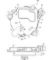
最初に、図1および図2を参照して、本実施形態に係る電子装置の概略構成について説明する。First Embodiment
First, the schematic configuration of the electronic device according to the present embodiment will be described with reference to FIGS. 1 and 2.
図1に示すように、電子装置100は、筐体10、カバー20およびコネクタ30を備え、回路基板40(図1において不可視)およびコンポーネントの一部である図示しないモータを備えている。筐体10およびカバー20はともに金属製である。その材料は例えばアルミであり、ダイカストによって所定の形状に成形されている。コネクタ30は樹脂製であり、筐体10に嵌合して一体のモジュールを成す。コンポーネントとは、上記のモータを含む概念であり、例えば、モータのような可動要素のほか、コネクタやバスバー、パワーモジュールなどの電気的要素も含む。 As shown in FIG. 1, the
筐体10は、回路基板40を収容する第1筐体11と、モータを収容する第2筐体12とを有している。図2に示すように、第1筐体11は有底の略円筒状であり、筒内に回路基板40を収容する収容空間11aを有する。回路基板40はその表面および裏面にマイコンやディスクリート部品などの電子部品が実装され、収容空間11aに収容された回路基板40は第1筐体11の底面11bにねじ留めされる。回路基板40にはコネクタ30から延びた図示しないリード線が接続され、外部機器との電気的な通信が可能になっている。また、底面11bのうち、収容空間11aを構成する面の一部には貫通孔11hが設けられ、第1筐体11の外側に設けられたモータから延びる制御端子が貫通孔11hを通って収容空間11a側に進入し、図示しないコネクタを介して回路基板40に接続されている。 The
また、第1筐体11は、中央近傍にベアリングを収容する軸受収容部11cと、他の部材に第1筐体11をねじ留めするための固定穴11dとを有している。 In addition, the
さらに、本実施形態における第1筐体11は、後述するカバー20に設けられた突出部21が嵌合される受け部50と、後述する弾性部22を収容する凹部51とを有している。突出部21、弾性部22、受け部50、凹部51およびその近傍の詳細な構造については後述する。 Furthermore, the
モータは第1筐体11の底面11bの外側の面に取り付けられるものであり、図示しないシャフトがベアリングとともに軸受収容部11cに収容されるように配置される。モータから延びる制御端子は、底面11bに設けられた貫通孔に挿通して回路基板40に至る。第2筐体12はモータの外側を覆うように第1筐体11に固定され、全体として一体的な筐体30の体をなす。すなわち、回路基板40とコンポーネントたるモータとは、第1筐体11の底面11bを隔壁とする2つの収容空間にそれぞれ収容されている。 The motor is attached to the outer surface of the
カバー20は、図1に示すように、第1筐体11の開口を覆うようにして固定され、回路基板40の収容空間を外部空間から隔離するものである。カバー20により収容空間に蓋をすることで回路基板40の防埃防塵を実現する。 As shown in FIG. 1, the
図1および図3に示すように、カバー20は、突出部21と、弾性部22と、変形抑制部23と、を有している。第1筐体11は、突出部21に対応する受け部50と、弾性部22に対応する凹部51とを有している。突出部21を受け部50に押し込むことで嵌合し、カバー20が第1筐体11に固定される。 As shown in FIGS. 1 and 3, the
本実施形態の突出部21は、カバー20の外縁近傍に設けられ円柱状に突起した部分である。突出部21はプレス加工等の方法により筐体10の収容空間側に突出するように成形されている。 The
弾性部22は、突出部21を受け部50に押し込む際に、突出部21に印加される力によるカバー20の変形を緩和するものである。具体的には、突出部21の形成位置を中心とした放射方向に直交する方向に延びて、図3に示すような、突出部21の形成位置を支点とし突出部21の突出方向を向く曲げの力Fに対して弾性変形可能に形成されている。本実施形態の弾性部22は、突出部21が形成された部分の周囲に形成され、より具体的には、突出部21のまわりを囲むように円環状に形成されている。突出部21がカバー20の外縁に設けられているため、弾性部22は、カバー20が存在していない部分には当然形成されず、図1に示すように、カバー20が存在する部分にC字状に形成されている。 The
弾性部22は、突出部21を筐体10側に押し込むエネルギーが、カバー20における弾性部22より外側の部分に伝播しにくいように、弾性エネルギーとして吸収可能な形状であれば良いが、例えば図3に示すように、V字状に曲げられた形状を採用することができる。本実施形態における弾性部22は、回路基板40に対向する対向面20aを正面視したとき、対向面20aに対してカバー20を構成する面が山折りされて弾性を有するようにされている。すなわち、カバー20には、突出部21の周囲に全周に亘ってV字状の折り曲げ部が形成されることによって弾性部22が構成されている。 The
突出部21および弾性部22の形状に対応して、第1筐体11には受け部50および凹部51が形成されている。受け部50は円筒状であり、受け部50に円柱状の突出部21が押し込まれることによって両者間のクリアランスが無くなり接合するようになっている。凹部51は、突出部21の周囲に形成された弾性部22に対応して、受け部50の周囲に円環状に形成されている。とくに、本実施形態では弾性部22がC字状に形成されているので、凹部51もこれに対応して、図2に示すようなC字状の構造になっている。凹部51は山折りに曲げられた弾性部22の収容空間側先端が第1筐体11に接触しないように設けられたものであり、これにより、弾性部22は弾性エネルギーを効率的に蓄積することができる。 A
カバー20は、突出部21が受け部50に押し込まれるとともに防水接着材24がカバー20と第1筐体11とを仲介して封止し、防水や防埃防塵の効果を奏する。 In the
さらに、カバー20は、変形抑制部23を有している。変形抑制部23は回路基板40を収容する収容空間側に凸となるようにカバー20の平面の一部が変形されて形成されたリブである。図1に示すように、本実施形態では変形抑制部23は2箇所に形成されている。変形抑制部23は突出部21が形成された位置を中心にして放射方向に延びて形成され、カバー20を外部空間から正面視するとカプセル形状にくり貫かれたように形成されている。図3に示すように、変形抑制部23は、対向面20a側に突出するように凹んだ形状になっている。 Furthermore, the
変形抑制部23は、上記のとおり突出部21の形状位置を中心に放射方向に延びて形成され、細長い形状になっている。よって、図3に示すような、突出部21の形成位置を支点とし突出部21の突出方向を向く曲げの力Fに対する曲げ剛性は、変形抑制部23が形成されず単純な平面よりも大きくなっている。 The
なお、変形抑制部23の形成数は2つに限定されず、1つでも良いし、3つ以上形成されていても良い。また、変形抑制部23は、突出部21の形成位置と、板片部25の形成位置とを結ぶ直線状に延びて形成されているとより好ましい。 In addition, the number of formation of the deformation |
さらに、カバー20は、図1および図4に示すように、板片部25を有している。板片部25は、突出部21の形成位置を1点として、カバー20を3点で固定できる位置に形成されている。板片部25は、カバー20のうち収容空間11aを覆う部分の外縁から、収容空間11aを覆う面に対して略直角に突出して形成されている。板片部25は、例えばプレス加工によりカバー20の外縁から突出した翼様の形状を成形後、該翼様の部分を筐体10側に折り曲げることによって形成することができる。板片部25は、カバー20が第1筐体11に固定される際に第1筐体11の側壁11fと擦れる程度に形成されている。つまり、板片部25は曲げによる弾性によって側壁11fを付勢した状態で固定されるのであり、カバー20の固定時には側壁11fとの間で摩擦固定が成される。 Furthermore, the
コネクタ30は、樹脂製のケースに図示しないリード線等が格納されて成る。ケースは筐体10のうち第1筐体11に嵌合するように成形されており、カバー20により第1筐体11が蓋される際に第1筐体11とカバー20に挟まれて固定される。コネクタ30が備えるリード線は回路基板40に接続されて回路基板40に実装されたマイコンなどの電子部品に接続される。回路基板40はコネクタ30を介して外部に設けられた電源や他の電子装置と相互に接続される。 The
次に、本実施形態における電子装置100を採用することによる作用効果について説明する。 Next, an operation and effect by adopting the
本実施形態におけるカバー20は、突出部21を有し、突出部21が筐体10に設けられた受け部50に嵌合することによってカバー20が固定される。突出部21は、例えばダイカストやプレス加工によって比較的容易に形成できるものである。よって、従来のように、カバーあるいは筐体のいずれかの部材に爪部とその受け部を形成する態様に較べて、安価にカバー20の固定に係る部分を形成することができる。 The
また、カバー20の筐体10への固定に際しては、筐体10の外縁より内側に形成された受け部50に対して、カバー20に形成された突出部21を嵌合させて固定するため、カバー20の固定に係る部分が筐体10の外縁より外側に飛び出ることはない。つまり、従来のようにカバーをかしめ固定するための拡張部を筐体の外周に外側に突出して設ける必要がない。このため、筐体10の体格を従来よりも小さくすることができ、電子装置100の設置場所について省スペース化ができるとともに、電子装置100の設置の自由度を向上させることができる。 Further, when the
さらに、カバー20は変形抑制部23を有している。変形抑制部23は、突出部21の形状位置を中心に放射方向に延びて形成され、細長い形状になっている。よって、突出部21の形成位置を支点とし突出部21の突出方向を向く曲げの力に対する曲げ剛性が、変形抑制部23が形成されず単純な平面よりも大きくなっている。このため、突出部21を受け部50に押し込む際のカバー20の平面の変形量を、変形抑制部23が形成されない態様に較べて抑制することができる。カバー20の変形量が抑制できることにより、電子装置100の近傍に配置された他の部品や部材への干渉を抑制することができる。変形抑制部23は、突出部21の形状位置を中心に放射方向に延びて形成されることが好ましいが、さらに好ましくは、上記したように、突出部21の形成位置と、板片部25の形成位置とを結ぶ直線状に延びて形成されているとよい。カバー20を曲げる応力は、カバー20の押し込み時に直接力が加わる突出部21と、摩擦により力が加わる板片部25において働くことが想定される。これに対して、突出部21の形成位置と、板片部25の形成位置とを結ぶ直線状に変形抑制部23が形成されることで、カバー20に印加される力に対して曲げ剛性を高めることができる。 Furthermore, the
さらに、カバー20は弾性部22を有している。弾性部22は、突出部21を筐体10側に押し込むエネルギーを、カバー20における弾性部22より外側の部分に伝播しにくいように、弾性エネルギーとして吸収する。このため、突出部21を受け部50に押し込む際のカバー20の平面の変形量を、弾性部22が形成されない態様に較べて抑制することができる。 Furthermore, the
弾性部22は、突出部21の形成位置を中心とした放射方向に直交する周方向に沿って少なくとも一部形成されていれば上記の効果を奏するが、より好ましくは、本実施形態における弾性部22のように、突出部21の周囲の全周に亘って形成されていると、カバー20を押し込むエネルギーを弾性エネルギーへの変換をより効果的におこなうことができる。 The
さらに、筐体10は、カバー20が接触する第1筐体11において、弾性部22に対応した凹部51を有している。凹部51はカバー20の対向面20aから内側に突出して形成された弾性部22の先端が第1筐体11に接触しないように設けられたものである。これにより、弾性部22が第1筐体11に対して宙に浮いた状態を維持できるので、弾性部22は弾性エネルギーを効率的に蓄積することができる。 Furthermore, the
なお、上記のように弾性部22は第1筐体11から完全に浮いた状態であることが好ましいが、図3に示すように、弾性部22の一部に防水接着材24が接触しても、弾性部22が直接第1筐体11に接触するような態様に較べて、弾性エネルギーを吸収する効果を奏する。これは、電子装置100の製造工程上、カバー20を筐体10に押し込んでから十分な時間が経過した後に防水接着材24が硬化するので、弾性部22は弾性エネルギーを吸収した形状で固定されるためである。すなわち、弾性部22が防水接着材24に接触することは、弾性エネルギーの吸収に対して影響を与えない。 In addition, although it is preferable that the
さらに、図4に示すように、筐体10は板片部25を有している。本実施形態における電子装置100は、1つの突出部21が受け部50に押し込まれることで嵌合し固定される。加えて、2つの板片部25が、突出部21と合わせて3点でカバー20を筐体10に固定する。板片部25は筐体10の側壁11fに接して摩擦固定されるので、突出部21の形成位置から遠い場所でもカバー20が反り上がることなく筐体10に蓋することができる。すなわち、弾性部22および変形抑制部23に加えて、板片部25を有することにより、カバー20の変形をより抑制することができる。 Furthermore, as shown in FIG. 4, the
また、突出部21の形成数は限定されないが、本実施形態のように、突出部21が1つだけ形成された態様では、突出部21の形成位置を中心にしてカバー20が筐体10に対して回転運動してしまう虞がある。これに対して、板片部25によりカバー20を筐体10に3点固定することで、カバー20の回転運動を抑制することができる。なお、回転運動の抑制という観点からは、突出部21を含めて少なくとも2点で固定されればその効果を発揮することができる。これに加えて、突出部21を含めて3点以上でカバー20を筐体10に固定することにより、カバー20を押し込むことによるカバー20の反りに起因する浮き上がりをより抑制することができる。 Although the number of
(第2実施形態)
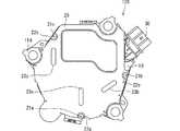
第1実施形態では、突出部21がカバー20の外縁近傍に形成され、板片部25とともにカバー20の外縁で筐体10に固定される例について説明した。これに対して、本実施形態における電子装置110は、図5に示すように、カバー20の略中央に1つの突出部21および弾性部22を有している。また、電子装置110は3つの板片部25を有している。Second Embodiment
In the first embodiment, the
弾性部22は突出部21の形成位置の周囲全周に亘って形成されている。加えて、電子装置110は、1つの変形抑制部23を有している。変形抑制部23は、第1実施形態と同様の形状を成し、突出部21の形成位置から放射方向に延びて形成されている。すなわち、変形抑制部23は、カバー20を外部空間から正面視するとカプセル形状にくり貫かれたように形成され、対向面20a側に突出するように凹んだ形状になっている。第1実施形態のように、複数の変形抑制部23が形成されていても良いが、1つであっても曲げ剛性を大きくできるので、突出部21を押し込むことによるカバー20の変形量を抑制することができる。また、複数の変形抑制部23を設けると、そのぶん筐体10に形成される収容空間11aの容積が減少してしまうため、変形抑制部23の形成数はできるだけ少ないほうが広い収容空間11aを確保することができる。 The
本実施形態における電子装置110も、3つの板片部25を有している。板片部25は、第1実施形態と同様に、カバー20の外縁に設けられ、第1筐体11の側壁11fに付勢するようになっている。板片部25は側壁11fに接触してカバー20を筐体10に摩擦固定している。すなわち、カバー20は、突出部21が受け部50に嵌合することによって固定されるとともに、3つの板片部25により摩擦固定され、合わせて4点で固定されている。 The
ところで、本実施形態における筐体10は、図6に示すように、側壁11fのうち板片部25が接触する部分の近傍に、側壁11fから外側にわずかに突出した突起部11gを有している。突起部11gは、突出部21の形成位置を回転中心としたカバー20の回転に伴う板片部25の軌道上において、板片部25の移動を妨げるようにして配置されている。すなわち、板片部25が突起部11gに当たることによって、カバー20がそれ以上回転しないようになっている。 By the way, as shown in FIG. 6, the
これによれば、例えば筐体10の受け部50に突出部21を押し込んだ後、意図的にカバー20を突出部21の形成位置を中心に回転させ、板片部25が突起部11gに当たったところでカバー20の回転を停止すれば、カバー20の位置を一意に決定することができる。 According to this, for example, after pushing the
このような突起部11gを有することによる効果は、本実施形態のように突出部21がカバー20の略中央に位置する態様において特に有意である。しかしながら、第1実施形態のように、突出部21がカバー20の外縁に形成されている態様であっても、突出部21が1つであるならば、突出部21の形成位置を中心にカバー20が回転する虞があるため、突起部11gを有することによりこの回転によるカバー20の位置ずれを抑制できる。 The effect of having such a
(第3実施形態)
第1実施形態および第2実施形態では、板片部25について、筐体10の側壁11fに対向する面と側壁11fとが面接触して摩擦固定に寄与する例を説明した。これに対して、本実施形態における板片部25は、図7に示すように、板片部25から側壁11f側に突出して接触するようにされた付勢部25aが設けられている。Third Embodiment
In the first embodiment and the second embodiment, an example in which the surface of the
本実施形態の付勢部25aは、板片部25の付け根の反対側である先端側近傍が折り曲げられて形成され、山折りにされた部分が側壁11fに線接触するようにされている。図7に示すように、本実施形態における板片部25は、付勢部25aによってカンチレバーのような構成となり、片持ち構造による板片部25の弾性によって付勢部25aが側壁11fに付勢されて、カバー20が筐体10に摩擦固定される。 The biasing
これによれば、第1実施形態や第2実施形態のように、板片部25が筐体10に対して面接触する態様に較べて、カバー20を筐体10に被せる際の位置決めにおいてクリアランスが生じるため、カバー20を筐体10に配置することが容易となる。 According to this, as in the first embodiment and the second embodiment, compared to the aspect in which the
(第4実施形態)
カバー20は、突出部21を複数有していても良い。図8および図9に示すように、本実施形態における電子装置120は、3つの突出部21と、突出部21に対応した3つの受け部50とを有している。なお、図8においては、3つの突出部21のそれぞれに符号21a,21b,21cを付与して示している。Fourth Embodiment
The
カバー20はその外縁部において互いに離れた位置に3つの突出部21を有しているので、カバー20は筐体10に対して3点固定される。これにより、突出部21が1つの態様に較べて、より強固にカバー20と筐体10とを固定することができる。また、3点で固定されることから、カバー20が回転方向にずれることも抑制できる。 The
また、カバー20は、それぞれの突出部21の形成位置の周囲に弾性部22が形成されている。具体的には、突出部21aの周囲に弾性部22aが形成され、突出部21bの周囲に弾性部22bが形成され、突出部21cの周囲に弾性部22cが形成されている。これにより、突出部21を筐体10に押し込む際にカバー20に与えられるエネルギーを弾性エネルギーとして弾性部22に吸収させることができ、カバー20の変形を抑制することができる。本実施形態における弾性部22は、カバー20の外縁に形成されているので、突出部21の形成位置の周囲全周に亘っては形成されず、一部が欠けたC字状に形成されている。 Further, in the
図9に示すように、カバー20に形成された突出部21に対応して、筐体10は3つの受け部50を有し、さらに、それぞれの受け部50の周囲に、弾性部22に対応した凹部51を有している。各凹部51は、弾性部22の形成位置に応じて第1筐体11の外縁に形成されるので、弾性部22と同様にC字状に形成されている。 As shown in FIG. 9, the
さらに、本実施形態におけるカバー20は、3つの変形抑制部23を有している。具体的には、突出部21aの形成位置の放射線上に長細く延びて形成された変形抑制部23aと、突出部21bの形成位置の放射線上に長細く延びて形成された変形抑制部23bと、突出部21cの形成位置の放射線上に長細く延びて形成された変形抑制部23cと、を有している。上記した各実施形態と同様に、カバー20は、変形抑制部23が形成されていることにより、カバー20が単なる平面である態様に較べて曲げ剛性を大きくできるので、突出部21が受け部50に押し込まれる際に印加される力に対して、カバー20の変形量を抑制することができる。 Furthermore, the
なお、複数の突出部21を有する態様における変形抑制部23について、必ずしも、1つの突出部21に対応して1つ以上の変形抑制部23が形成される必要はない。つまり、例えば本実施形態の電子装置120において、変形抑制部23cが形成されず、カバー20が変形抑制部23a,23bのみを有する態様でも良い。 In addition, about the deformation |
また、電子装置120におけるカバー20は、3つの突出部21によって筐体10に3点固定が可能なため、固定を補助する板片部25を有していないが、板片部25の存在を否定するものではなく、カバー20の外縁に形成されていても良い。 In addition, the
(その他の実施形態)
この明細書および図面等における開示は、例示された実施形態に制限されない。開示は、例示された実施形態と、それらに基づく当業者による変形態様を包含する。例えば、開示は、実施形態において示された部品および/または要素の組み合わせに限定されない。開示は、多様な組み合わせによって実施可能である。開示は、実施形態に追加可能な追加的な部分をもつことができる。開示は、実施形態の部品および/または要素が省略されたものを包含する。開示は、ひとつの実施形態と他の実施形態との間における部品および/または要素の置き換え、または組み合わせを包含する。開示される技術的範囲は、実施形態の記載に限定されない。開示されるいくつかの技術的範囲は、請求の範囲の記載によって示され、さらに請求の範囲の記載と均等の意味及び範囲内での全ての変更を含むものと解されるべきである。(Other embodiments)
The disclosure in this specification, the drawings and the like is not limited to the illustrated embodiments. The disclosure includes the illustrated embodiments and variations based on them by those skilled in the art. For example, the disclosure is not limited to the combination of parts and / or elements shown in the embodiments. The disclosure can be implemented in various combinations. The disclosure can have additional parts that can be added to the embodiments. The disclosure includes those in which parts and / or elements of the embodiments have been omitted. The disclosure includes replacements or combinations of parts and / or elements between one embodiment and another embodiment. The disclosed technical scope is not limited to the description of the embodiments. It is to be understood that the technical scopes disclosed herein are indicated by the description of the scope of the claims, and further include all modifications within the meaning and scope equivalent to the descriptions of the scope of the claims.
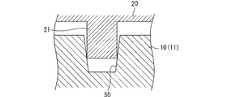
上記した各実施形態において、受け部50は円筒状にくり貫かれた構造として例示したが、図10に示すように、内壁がテーパを持って形成されても良い。この受け部50は、開口の直径が突出部21の直径よりも大きくされ、下方にいくにしたがって幅縮して突出部21の直径とほぼ同一か、あるいはやや小さい程度にされている。これにより、突出部21は、嵌め込まれる過程で受け部50に押圧され、変形しつつ受け部50と嵌合する。 In each of the above-described embodiments, the receiving
また、上記した各実施形態において、第1筐体11の側壁11fは、板片部25が接触する部分において、カバー20の平面に対して直角に切り立った構造として例示したが、図11に示すように、高勾配のテーパ形状にしても良い。板片部25は、カバー20が筐体10に嵌合する際に、側壁11fに面接触しながら弾性的に変形して筐体10を側面から挟むようにされる。これにより、側壁11fが垂直に切り立った態様に較べて、板片部25が側壁11fから受ける垂直抗力を大きくでき、摩擦力を大きくすることができる。よって、カバー20の筐体10に対する固定強度を大きくすることができる。 Further, in each of the embodiments described above, the
また、上記した各実施形態において、変形抑制部23であるリブや突出部21が、カバー20を構成する平面の一部をプレス変形して形成した例について説明したが、この例に限定されない。例えば図12に示すように、カバー20の平面の一部を厚くすることによって変形抑制部23を構成しても良い。この態様では、変形抑制部23は、カバー20の平面の一部が厚くなった部分が突出部21の形成位置から放射方向に延びた形状となっている。これにより、単なる平面形状に較べて、曲げ剛性を大きくすることができる。この他、単なる平面形状である態様に較べて曲げ剛性が大きくなる構造であれば、任意の構造を採用することができる。しかしながら、カバー20をプレス加工することによって変形抑制部23を形成できれば、他のプレス加工工程と工程を共通化できるなどのメリットがある。また、各実施形態では、変形抑制部23としてのリブが、回路基板40が収容される収容空間11a側に飛び出るように形成される例を示したが、収容空間11a側に空間的な余裕がない場合には、収容空間11aとは反対側、すなわち外部に向けて飛び出るようにリブを形成しても良い。 Further, in each of the above-described embodiments, although the rib or the
また、上記した各実施形態においては、弾性部22が突出部21の形成位置の周囲に形成される例について説明したが、同様の効果を奏する弾性部が板片部25の周囲にも形成されているとより好ましい。カバー20が筐体10に押し込まれる際には、筐体10との間で摩擦固定される板片部25にもカバー20を変形させうる応力が生じるので、突出部21の周囲だけでなく板片部25の周囲にも弾性部を有する態様が好ましい。また、同様の理由により、板片部25の形成位置を中心とした放射方向に延びる変形抑制部23が形成されているとより好ましい。よって、上記したように、変形抑制部23は、突出部21の形成位置と、板片部25の形成位置とを結ぶ直線状に延びて形成されているとよい。 In each of the above-described embodiments, the
10…筐体,11…第1筐体,12…第2筐体,20…カバー,21…突出部,22…弾性部,23…変形抑制部,30…コネクタ,40…回路基板,50…受け部,51…凹部DESCRIPTION OF
Claims (10)
Translated fromJapanese前記筐体を蓋して前記回路基板を保護する金属製のカバー(20)と、を備え、
前記カバーが前記回路基板を収容する収容空間(11a)側に突出する突出部(21)を有するとともに、前記筐体は前記突出部に対応する位置に、前記突出部が嵌合する受け部(50)を有し、
前記カバーは、前記回路基板に対向する対向面(20a)において、前記突出部の形成位置を支点とし前記突出部の突出方向を向く曲げに対する曲げ剛性が平面構造よりも大きくなるように形成された変形抑制部(23)を有する、電子装置。A metal case (10) in which the components and the circuit board (40) are accommodated with the partition wall (11b) separated;
And a metal cover (20) for covering the housing and protecting the circuit board.
The cover has a projecting portion (21) projecting toward the accommodation space (11a) that accommodates the circuit board, and the housing is a receiving portion in which the projecting portion is fitted at a position corresponding to the projecting portion ( 50),
The cover is formed such that the bending rigidity against bending in the direction of protrusion of the protrusion is higher than that of the planar structure on the facing surface (20a) facing the circuit board with the formation position of the protrusion as a fulcrum Electronic apparatus which has a deformation | transformation suppression part (23).
前記板片部は、少なくとも一部が前記筐体の側壁に接触して摩擦固定される、請求項1〜4のいずれか1項に記載の電子装置。The cover has a plate portion (25) formed to project along at least a part of the outer edge along the side wall (11f) of the housing;
The electronic device according to any one of claims 1 to 4, wherein at least a part of the plate piece portion is frictionally fixed in contact with a side wall of the housing.
前記筐体の側壁は、前記板片部が接触する部分の近傍であって、前記突出部の形成位置を回転中心とした前記カバーの回転に伴う前記板片部の軌道上に突起部(11g)を有する、請求項5または請求項6に記載の電子装置。In the case where the cover has only one protrusion,
The side wall of the housing is in the vicinity of the portion where the plate piece contacts, and a protrusion (11g) is formed on the track of the plate piece with the rotation of the cover centering on the formation position of the protrusion. The electronic device according to claim 5 or 6, further comprising
Priority Applications (2)
| Application Number | Priority Date | Filing Date | Title |
|---|---|---|---|
| JP2017229423AJP2019102545A (en) | 2017-11-29 | 2017-11-29 | Electronic device |
| US16/168,274US10420229B2 (en) | 2017-11-29 | 2018-10-23 | Electronic device |
Applications Claiming Priority (1)
| Application Number | Priority Date | Filing Date | Title |
|---|---|---|---|
| JP2017229423AJP2019102545A (en) | 2017-11-29 | 2017-11-29 | Electronic device |
Publications (1)
| Publication Number | Publication Date |
|---|---|
| JP2019102545Atrue JP2019102545A (en) | 2019-06-24 |
Family
ID=66632947
Family Applications (1)
| Application Number | Title | Priority Date | Filing Date |
|---|---|---|---|
| JP2017229423APendingJP2019102545A (en) | 2017-11-29 | 2017-11-29 | Electronic device |
Country Status (2)
| Country | Link |
|---|---|
| US (1) | US10420229B2 (en) |
| JP (1) | JP2019102545A (en) |
Families Citing this family (3)
| Publication number | Priority date | Publication date | Assignee | Title |
|---|---|---|---|---|
| JP7159834B2 (en)* | 2018-12-11 | 2022-10-25 | 日本電産株式会社 | Baseplate and hard disk drive |
| TW202517504A (en)* | 2019-12-27 | 2025-05-01 | 日商島野股份有限公司 | Components and gears for human-powered vehicles |
| KR102351834B1 (en)* | 2020-02-13 | 2022-01-14 | 엘에스일렉트릭(주) | Electronic control device |
Family Cites Families (7)
| Publication number | Priority date | Publication date | Assignee | Title |
|---|---|---|---|---|
| JP2007005729A (en) | 2005-06-27 | 2007-01-11 | Murata Mfg Co Ltd | Resin package |
| JP4725388B2 (en) | 2006-03-28 | 2011-07-13 | 三菱自動車工業株式会社 | Vehicle door structure |
| JP2012155986A (en) | 2011-01-26 | 2012-08-16 | Sanyo Electric Co Ltd | Power source device |
| CN110083212B (en)* | 2013-05-17 | 2023-07-14 | 索尼电脑娱乐公司 | Electronic equipment |
| JP6449694B2 (en)* | 2015-03-18 | 2019-01-09 | 日立オートモティブシステムズ株式会社 | Electronic control unit |
| JP6616493B2 (en)* | 2016-03-31 | 2019-12-04 | 株式会社ソニー・インタラクティブエンタテインメント | Electronics |
| US10206295B2 (en)* | 2016-08-19 | 2019-02-12 | Flextronics Ap, Llc | Securing a PCB in a plastic and metal housing |
- 2017
- 2017-11-29JPJP2017229423Apatent/JP2019102545A/enactivePending
- 2018
- 2018-10-23USUS16/168,274patent/US10420229B2/enactiveActive
Also Published As
| Publication number | Publication date |
|---|---|
| US20190166705A1 (en) | 2019-05-30 |
| US10420229B2 (en) | 2019-09-17 |
Similar Documents
| Publication | Publication Date | Title |
|---|---|---|
| US10292281B2 (en) | Electronic control device | |
| US11758667B2 (en) | Electronic control unit | |
| JP2019102545A (en) | Electronic device | |
| JP6531628B2 (en) | Case closing structure | |
| JP2020124046A (en) | Electric actuator | |
| JP6148598B2 (en) | connector | |
| JP2020124045A (en) | Electric actuator | |
| JP4866830B2 (en) | Automotive electronics | |
| JP5708969B2 (en) | Optical encoder | |
| JP4684340B2 (en) | Molded motor | |
| JP2023001851A (en) | Busbar cover and busbar routing structure | |
| JP5056694B2 (en) | Bending piping, bent piping assembly and hot water supply device | |
| JP4362421B2 (en) | motor | |
| JP5011794B2 (en) | Electric power steering device | |
| CN107514364B (en) | A kind of compressor | |
| JP2018105264A (en) | Motor compressor | |
| JP6087443B2 (en) | Stator, electric motor and air conditioner | |
| JP6037850B2 (en) | Grommet | |
| JP2017180213A (en) | Electric compressor | |
| JP5242297B2 (en) | Electrical junction box | |
| JP7200481B2 (en) | electronic device | |
| JP2009100593A (en) | Brush holder | |
| JP6263057B2 (en) | Connector connection structure | |
| JP2006014462A (en) | Motor and manufacturing method thereof | |
| CN218633532U (en) | Motor |