JP2019086821A - Communication medium - Google Patents
Communication mediumDownload PDFInfo
- Publication number
- JP2019086821A JP2019086821AJP2017211863AJP2017211863AJP2019086821AJP 2019086821 AJP2019086821 AJP 2019086821AJP 2017211863 AJP2017211863 AJP 2017211863AJP 2017211863 AJP2017211863 AJP 2017211863AJP 2019086821 AJP2019086821 AJP 2019086821A
- Authority
- JP
- Japan
- Prior art keywords
- coil
- communication medium
- communication
- flat plate
- plate electrode
- Prior art date
- Legal status (The legal status is an assumption and is not a legal conclusion. Google has not performed a legal analysis and makes no representation as to the accuracy of the status listed.)
- Pending
Links
Images


Landscapes
- Credit Cards Or The Like (AREA)
- Near-Field Transmission Systems (AREA)
Abstract
Translated fromJapaneseDescription
Translated fromJapanese本発明は、非接触型通信が可能な通信媒体に関する。 The present invention relates to a communication medium capable of contactless communication.
接触通信機能、および非接触通信機能を有するICチップを搭載したデュアルインターフェース型のICモジュールを製造し、そのICモジュールを組込んだICカード等のデュアルインターフェース型の通信媒体が製造されている。 A dual interface type IC module mounted with an IC chip having a contact communication function and a non-contact communication function is manufactured, and a dual interface communication medium such as an IC card incorporating the IC module is manufactured.
ここで、カード本体のアンテナ回路と電磁結合によって結合する、磁界接続コイルを有する電磁結合式のICモジュールを用いると、ICモジュールとカード本体の通信用コイルが直接には接合しないので、接合部へのストレスによりICモジュールとカード本体との電気的な結合が不安定になる問題が解決できる。 Here, when using an electromagnetic coupling type IC module having a magnetic field connection coil, which is coupled to the antenna circuit of the card main body by electromagnetic coupling, the communication coil for the IC module and the card main body is not directly joined. Can solve the problem that the electrical connection between the IC module and the card body becomes unstable due to stress.
ICモジュールが持つ磁界接続コイルとカード本体とが電磁結合により電気的に結合された通信媒体としては、例えば特許文献1から3に記載された通信媒体が知られている。 As communication media in which a magnetic field connection coil of an IC module and a card body are electrically coupled by electromagnetic coupling, communication media described in Patent Documents 1 to 3, for example, are known.
磁界接続コイルを有する電磁結合式のICモジュールには、カード本体のアンテナ回路の配線との電磁結合を介して電力が供給され、また、その電磁結合を介して、ICモジュールがカード本体の通信用コイルとの間で通信用の信号を送受信することができる。 The electromagnetic coupling type IC module having the magnetic field connection coil is supplied with power through electromagnetic coupling with the wiring of the antenna circuit of the card main body, and through the electromagnetic coupling, the IC module is used for communication of the card main body. A signal for communication can be transmitted and received with the coil.
特許文献1の通信媒体では、カード本体内のアンテナ基板の面に形成した結合用コイルとトランス結合(電磁結合)する磁界接続コイルを持つICモジュールを用い、カード本体のアンテナ基板においては、その結合用コイルとアンテナコイルと共振用容量性素子を並列に接続して共振回路が形成されていた。 The communication medium of Patent Document 1 uses an IC module having a magnetic field connecting coil which is coupled with a coupling coil formed on the surface of an antenna substrate in a card body and a transformer coil (electromagnetic coupling), and the antenna substrate of the card body is coupled A resonant circuit is formed by connecting in parallel the for-use coil, the antenna coil and the resonant capacitive element.
そのICモジュールでは、接触型外部機器との接触インターフェース用の端子(外部接触端子部)が表面に形成されており、そのICモジュールの側面あるいは裏面にトランス結合用の磁界接続コイルが形成されている。 In the IC module, a terminal (external contact terminal portion) for contact interface with a contact type external device is formed on the surface, and a magnetic connection coil for transformer coupling is formed on the side surface or the back surface of the IC module .
この通信媒体では、ICモジュールが持つ磁界接続コイルの巻き数とカード本体の結合用コイルの巻き数とを調整することによって、インピーダンスマッチングをとり、ICチップへの電力供給を最適化している。 In this communication medium, impedance matching is performed by adjusting the number of turns of the magnetic field connection coil of the IC module and the number of turns of the coupling coil of the card body, and power supply to the IC chip is optimized.
一方、カード本体に対するICモジュールの配置が規格(JIS X6320−2:2009(ISO/IEC7816:2007))により決まっていたり、カード本体にエンボスが形成可能なエンボス領域(例えば、JIS X6302−1:2005(ISO/IEC 7811−1:2002))を設ける必要がある。 On the other hand, the arrangement of the IC module with respect to the card body is determined by the standard (JIS X6320-2: 2009 (ISO / IEC 7816: 2007)), or an embossed area (e.g. JIS X6302-1: 2005) in which embossing can be formed on the card body. It is necessary to provide (ISO / IEC 7811-1: 2002).
しかし、共振用容量性素子が内蔵されている部分にエンボス加工が施されてしまうと、
加圧プレスにより共振用容量性素子の平板電極間の距離が変化することで共振用容量性素子の静電容量が変化してしまう。その結果、通信性能が完成品として想定していた範囲より逸脱してしまう可能性がある問題があった。However, if the part where the resonant capacitive element is built in is embossed,
When the distance between the flat plate electrodes of the capacitive element for resonance is changed by pressing and pressing, the capacitance of the capacitive element for resonance is changed. As a result, there is a problem that the communication performance may deviate from the range assumed as a finished product.
そのため、共振用容量性素子のパターンを避けた位置にエンボス加工を行う必要があるが、共振用容量性素子のパターンが占有する面積が広いため、エンボス加工を行える領域が狭くなる問題があった。また、ICモジュールが持つ磁界接続コイルとトランス結合するためのカード本体における結合用コイルも、エンボス加工を行える領域を狭くするため、結合用コイルの配置位置も制限され、その配置の自由度が低くなるという問題があった。 Therefore, it is necessary to emboss at a position avoiding the pattern of the capacitive element for resonance, but there is a problem that the area where embossing can be performed becomes narrow because the area occupied by the pattern of the capacitive element for resonance is large. . In addition, since the coupling coil in the card body for transformer coupling with the magnetic field connection coil of the IC module also narrows the area where embossing can be performed, the arrangement position of the coupling coil is also limited, and the degree of freedom in the arrangement is low. There was a problem of becoming
本発明は、このような問題点に鑑みてなされたものであって、幅広い周波数領域でアンテナ利得が高く良好な通信が可能で、かつ、エンボス加工を行える領域を広くした通信媒体を提供することを目的とする。 The present invention has been made in view of such problems, and provides a communication medium in which the antenna gain is high in a wide frequency range, high communication is possible, and the area in which embossing can be performed is widened. With the goal.
上記課題を解決するために、本発明は、ICモジュールをカード本体に設置して成る通信媒体であって、
前記ICモジュールが持つ磁界接続コイルと前記カード本体の結合用コイルをトランス結合させ、
前記カード本体の前記結合用コイルと並列に接続した通信用コイルと共振用容量性素子を有し、
前記通信用コイルが前記結合用コイルを囲んで巻かれ、前記結合用コイルと前記通信用コイルは互いに逆方向に巻かれていることを特徴とする通信媒体である。In order to solve the above problems, the present invention is a communication medium in which an IC module is installed in a card body,
Transformer coupling between a magnetic field connection coil of the IC module and a coupling coil of the card body;
A communication coil connected in parallel with the coupling coil of the card body and a capacitive element for resonance;
A communication medium is characterized in that the communication coil is wound around the coupling coil, and the coupling coil and the communication coil are wound in opposite directions.
本発明は、この構成により、幅広い周波数領域でアンテナ利得が高く、良好な通信が可能になる効果がある。 The present invention is advantageous in that the antenna gain is high in a wide frequency range and good communication is possible by this configuration.
また、本発明は、上記の通信媒体であって、前記通信用コイルの配線の一部を太らせた部分を、前記共振用容量性素子を構成する対向する平板電極の一部と共用させたことを特徴とする通信媒体である。 Further, according to the present invention, in the communication medium described above, a part obtained by thickening a part of the wire of the communication coil is shared with a part of the opposing flat plate electrode which constitutes the capacitive element for resonance. It is a communication medium characterized by the above.
また、本発明は、上記の通信媒体であって、前記結合用コイルが、アンテナ基板の上面側の結合用コイルと下面側の結合用コイルとの2層のコイルで構成されていることを特徴とする通信媒体である。 Further, according to the present invention, in the communication medium described above, the coupling coil is constituted by a two-layer coil of a coupling coil on the upper surface side of the antenna substrate and a coupling coil on the lower surface side. Communication media.
また、本発明は、上記の通信媒体であって、前記共振用容量性素子が、固定容量部平板電極のパターンと可変容量部複数平板電極パターンを有し、前記可変容量部複数平板電極パターンを、複数の平板電極を前記通信媒体の長手方向に配列して骨格用配線パターンで連結し、前記骨格用配線パターンと前記固定容量部平板電極のパターンを前記通信媒体の長手方向の何れか一方の端の通信用コイルに接続して連結したことを特徴とする通信媒体である。 The present invention is the communication medium as described above, wherein the resonant capacitive element has a pattern of a fixed capacitance flat electrode and a variable capacitance multiple flat electrode pattern, and the variable capacitance multi flat electrode pattern A plurality of flat plate electrodes are arranged in the longitudinal direction of the communication medium and connected by a skeletal wiring pattern, and the pattern of the skeletal wiring pattern and the pattern of the fixed capacitance portion flat electrode is either one of the longitudinal direction of the communication medium A communication medium characterized by being connected and connected to a communication coil at one end.
また、本発明は、上記の通信媒体であって、前記固定容量部平板電極のパターンが、前記カード本体の署名禁止領域内に形成されていることを特徴とする通信媒体である。 Further, the present invention is the communication medium as described above, wherein the pattern of the fixed capacitor portion flat plate electrode is formed in a signature prohibited area of the card body.
また、本発明は、上記の通信媒体であって、前記署名禁止領域の外に形成された前記可変容量部複数平板電極パターンの、前記通信媒体の長手方向の長さを、前記固定容量部平板電極のパターンの前記通信媒体の長手方向の長さより短く形成し、該長さの差分の領域に追加加工のエンボス加工領域を設けたことを特徴とする通信媒体である。 Further, according to the present invention, in the communication medium described above, the length in the longitudinal direction of the communication medium of the variable capacity portion plural flat plate electrode pattern formed outside the signature prohibited area is the fixed capacity portion flat plate. The communication medium is characterized in that the pattern of the electrode is formed shorter than the length in the longitudinal direction of the communication medium, and an embossed area for additional processing is provided in the area of the difference in length.
また、本発明は、上記の通信媒体であって、前記可変容量部複数平板電極パターンの前記骨格用配線パターンを切断することで、前記骨格用配線パターンが接続する通信用コイル側から遠い側の端の複数の平板電極のパターンを切り離し、該切り離された平板電極のパターンの領域にまで前記追加加工のエンボス加工領域を広げたことを特徴とする通信媒体である。 Further, according to the present invention, there is provided the communication medium as described above, wherein the skeleton wiring pattern of the plurality of flat plate electrode patterns of the variable capacitance portion is cut away from the communication coil side to which the skeleton wiring pattern is connected. A communication medium characterized in that a pattern of a plurality of flat plate electrodes at an end is separated and an embossed area of the additional processing is extended to the area of the pattern of the separated flat electrode.
本発明の通信媒体によれば、幅広い周波数領域でアンテナ利得が高く、良好な通信が可能になる効果がある。また、本発明によれば、通信媒体のカード本体における結合用コイルの配置の自由度を高めることができる効果がある。 According to the communication medium of the present invention, there is an effect that antenna gain is high in a wide frequency range and good communication is possible. Further, according to the present invention, it is possible to increase the degree of freedom in the arrangement of the coupling coil in the card body of the communication medium.
<第1の実施形態>
以下、本発明の通信媒体の第1の実施形態を、図1から図5を参照して説明する。図1は本発明のデュアルインターフェース型の通信媒体を模式的に示す断面図であり、図2は、その平面図である。図3はICモジュール20の平面図であり、図4は、カード本体10の内層に埋め込むアンテナ基板12の上面と下面の平面図である。図5は、等価回路図である。First Embodiment
Hereinafter, a first embodiment of the communication medium of the present invention will be described with reference to FIGS. 1 to 5. FIG. 1 is a cross-sectional view schematically showing a dual interface communication medium of the present invention, and FIG. 2 is a plan view thereof. FIG. 3 is a plan view of the
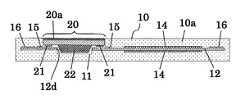
図1の断面図および図2の平面図に示すように、本発明のICカードタイプの通信媒体は、板状のカード本体10の凹部11にICモジュール20を設置して収納している。 As shown in the cross-sectional view of FIG. 1 and the plan view of FIG. 2, the IC card type communication medium of the present invention has the
図2の平面図では、カード本体10に埋め込んだICモジュール20の、カード本体10の表面に露出した接触式の外部接触端子20aと、カード本体10の内層に埋め込まれたアンテナ基板12に形成した結合用コイル15と通信用コイル16と共振用容量性素子
14を透視図で示す。In the plan view of FIG. 2, the
カード本体10は、図1の断面図のように、カード基材10a内に絶縁性のアンテナ基板12を埋め込み、また、カード基材10aに凹部11を設け、その凹部11にICモジュール20を収納して構成する。 In the
カード基材10a及びアンテナ基板12に用いる材料は、非晶質ポリエステルなどのポリエステル系材料、PVC(ポリ塩化ビニル)などの塩化ビニル系材料、ポリカーボネート系材料、PET(ポリエチレンテレフタレート)やPET−G(ポリエチレンテレフタレート共重合体)やポリエチレンナフタレート(PEN)などの、カード本体10やアンテナ基板12として一般的な絶縁性や耐久性を兼ね備えた材料を用いる。 Materials used for the
また、カード本体10には、エンボスが形成可能なエンボス加工領域RがICカードの規格(X 6302−1:2005(ISO/IEC 7811−1:2002))に基づいて、下辺より24mmに設定されている。 In addition, in the
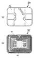
(ICモジュール20)
ICモジュール20は、図3(a)の平面図のように、外部の読取装置と接触型通信をするための外部接触端子20aをICモジュール20の基板上面に有する。そして、図3(b)の平面図のように、ICモジュール20の基板の下面に、非接触式通信部である磁界接続コイル21を設ける。図3(b)のICモジュール20の基板の下面の平面図は上面からの透視図で示す。(IC module 20)
As shown in the plan view of FIG. 3A, the
下面の磁界接続コイル21は、ICモジュール20のICチップ22の電極端子に電気接続する。この磁界接続コイル21は、図5の等価回路のように、アンテナ基板12の結合用コイル15とトランス結合(磁界結合)する。 The magnetic
また、図3(b)の平面図のように、ICモジュール20の基板の下面にICチップ22が設置され、樹脂で保護されている。ICモジュール20の基板の大きさは縦横9mm×11mmであり、その基板の下面に設置されたICチップ22の樹脂保護部分の大きさは縦横5mm×7mmある。 Further, as shown in the plan view of FIG. 3B, the
(アンテナ基板12)
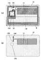
カード本体10の内層に埋め込むアンテナ基板12は、図4の平面図の様に、平面視で矩形状に形成する。アンテナ基板12の厚さは、例えば15〜50μm(マイクロメートル)である。(Antenna board 12)
The
図4(a)に、アンテナ基板12の上面の配線パターンを示し、図4(b)に、アンテナ基板12の下面の配線パターンを上面からの透視図で示す。アンテナ基板12の上面に、アンテナ回路として、結合用コイル15と、通信用コイル16と共振用容量性素子14を形成し、アンテナ基板12の下面に、立体交差させる配線と、アンテナ基板12の上面側の共振用容量性素子14と対向する共振用容量性素子14を形成する。 FIG. 4A shows a wiring pattern on the upper surface of the
この通信用コイル16と共振用容量性素子14と結合用コイル15によってブースタアンテナを構成する。通信用コイル16及び結合用コイル15は、直径30μm〜150μm程度の銅などのワイヤーにより形成してもよい。 A booster antenna is constituted by the
アンテナ基板12には、図1の断面図と図4の平面図の様に、ICモジュール20のICチップ22の樹脂保護部分を収容する位置に、アンテナ基板12の厚さ方向に貫通する収容孔12dを形成する。ICチップ22の樹脂保護部分の収容孔12dは、ICモジュ
ール20のICチップ22の樹脂保護部のサイズよりも同等かやや大き目に形成する。As shown in the cross-sectional view of FIG. 1 and the plan view of FIG. 4, the
アンテナ基板12の収容孔12dは、アンテナ基板12をカード基材10a内に埋め込んだ後でミリング加工、切削加工等のザグリ加工によりカード基材10aに凹部11を形成するのと同時に形成しても良い。 The
(共振用容量性素子14)
共振用容量性素子14を、図5の等価回路のように、アンテナ基板12の結合用コイル15、及び非接触型通信を行うための通信用コイル16に並列に接続する。共振用容量性素子14は静電容量を有し、結合用コイル15及び通信用コイル16に並列に接続した並列共振回路を構成する。(Resonant capacitive element 14)
The
共振用容量性素子14は、図4(a)に示すアンテナ基板12の上面と、図4(b)に示すアンテナ基板12の下面で対向させた幅広パターンによって形成する。その共振用容量性素子14の容量と、通信用コイル16のインダクタンスとで共振回路を形成する。 The
図5は、本発明の通信媒体の原理を説明するための等価回路図である。外部機器のリーダ/ライタの送受信回路が発生する高周波電磁界により、通信媒体の通信用コイル16に高周波電圧が誘起され、共振用容量性素子14の容量と、通信用コイル16のインダクタンスとで構成した共振回路に電流が流れる。 FIG. 5 is an equivalent circuit diagram for explaining the principle of the communication medium of the present invention. A high frequency voltage is induced in the
通信用コイル16と共振用容量性素子14の共振回路で受信した信号は、結合用コイル15に伝達される。そして、結合用コイル15とICモジュール20が持つ磁界接続コイル21との電磁結合によってICチップ22に信号が伝達される。 A signal received by the resonant circuit of the
共振用容量性素子14を結合用コイル15及び通信用コイル16に並列に接続してブースタアンテナを構成することで、共振用容量性素子14と結合用コイル15と通信用コイル16を直列に接続してブースタアンテナを構成した場合と比べて、同一共振周波数を有するL(コイル)とC(容量性素子の容量)による閉ループ共振回路のQ値を減らすことが可能となる。 The
ブースタアンテナの共振回路のQ値を減らすことで、製造公差に伴うブースタアンテナの共振周波数の変動に伴う通信特性への影響を減らすことができ、通信性能を安定させることが可能となる効果がある。 By reducing the Q value of the resonant circuit of the booster antenna, it is possible to reduce the influence on the communication characteristics due to the fluctuation of the resonant frequency of the booster antenna due to the manufacturing tolerance, and it is possible to stabilize the communication performance. .
実験の結果、本実施形態の構成で、共振用容量性素子14と通信用コイル16と結合用コイル15を並列に接続して共振回路を構成すると、その共振回路の共振点の周波数から2MHz以上離れた周波数領域において、それらを直列に接続して構成した共振回路よりも、アンテナ利得が高くなり、幅広い周波数領域で良好な通信が可能になる効果がある知見を得た。 As a result of the experiment, in the configuration of this embodiment, when the
これにより、本実施形態の構成は、幅広い周波数領域で良好な通信が可能であるため、製造公差に伴う通信用コイル16及び結合用コイル15の共振周波数の変動に伴う通信特性への影響を減らすことができ、通信性能を安定させることが可能になる効果がある。 Thereby, since the configuration of the present embodiment enables good communication in a wide frequency range, the influence on the communication characteristics due to the variation of the resonant frequency of the
(通信用コイル16)
アンテナ基板12における通信用コイル16は、非接触で外部機器のリーダ/ライタと通信し、結合用コイル15は、ICモジュール20が持つ磁界接続コイル21とトランス結合する。通信用コイル16と結合用コイル15は共振用容量性素子14に並列に接続してアンテナ回路の共振回路を構成する。(Coiling coil 16)
The
通信用コイル16は、図4(a)の平面図のように、結合用コイル15と共振用容量性素子14を囲む螺旋状の2巻きで形成し、通信用コイル16の外形の寸法を例えば、縦48.6mmで横79.6mmに形成する。 As shown in the plan view of FIG. 4A, the
通信用コイル16の配線幅は、エンボス加工領域Rの外で、カード本体10の外周に沿って配置される通信用コイル16の配線の幅を1mm以上の配線幅で形成することが望ましい。そうすることで配線の断線を防止できる効果がある。 As for the wiring width of the
図4(a)のように、エンボス加工領域R内では、通信用コイル16の配線幅を、エンボス加工領域Rの外での配線幅よりも広くする。エンボス加工領域R内で配線幅を広くすることで、エンボス加工領域Rにエンボスが形成されたときに配線が断線するのを防ぐことができる。 As shown in FIG. 4A, in the embossing region R, the wiring width of the
通信用コイル16の最も外側に配された端部には、通信用コイル16の配線幅よりも幅が広く略円形状に形成されたランド13cを設ける。ランド13cは、直径を2mm以上に形成し、ランド面内に設けた層間導通孔を介して、図4(b)の平面図のように、アンテナ基板12の下面のランド13dに電気接続して下面の配線に接続することで配線を立体交差させる。 At the outermost end of the
すなわち、このランド13cと20dはカード面の法線方向からの垂直視で互いに重なるように配置されており、ランド13c面上に設けた層間導通穴を介して反対側の面のランド13dに電気接続する。 That is, the
通信用コイル16と、その通信用コイル16が囲む結合用コイル15は、図4(a)のように、互いに逆方向に巻いて構成する。実験により、このように通信用コイル16が結合用コイル15を囲み、通信用コイル16と結合用コイル15の配線の方向を互いに逆方向に巻く構成のブースタアンテナの特性を解析した。 The
この様に構成することで、外部機器のリーダ/ライタから受ける磁界を通信用コイル16が受け取るだけでなく、結合用コイル15もリーダ/ライタから磁界を受け取り、互いに増幅する効果がある知見を得た。その結果、このブースタアンテナとICモジュール20が持つ磁界接続コイル21を組合せた際の非接触通信媒体の通信性能を向上させる効果がある。 With this configuration, not only the
すなわち、実験の結果、通信用コイル16と結合用コイル15の配線の方向を互いに同じ方向に巻いた場合と比べると、通信用コイル16のアンテナ利得が全周波数領域において高くなる効果がある知見を得た。 That is, as a result of the experiment, it is found that the antenna gain of the
また、通信用コイル16の巻数に関して実験した結果、巻き数が1.5巻きから2巻きで、アンテナ利得が最も高くなり、通信用コイル16の巻数がそれ以下またはそれ以上にするとアンテナ利得が低下する傾向がある知見を得た。 As a result of experiments on the number of turns of the
アンテナ利得の最大値からのアンテナ利得の低下が1dB程度までとなるコイルの巻数を実用的な構成であると考えると、通信用コイル16は、大きさがカードサイズ(85.6mm×54.0mm)以下であるが、概ね75mm×45mmよりも大きく、巻数が概ね1巻きから3巻きの間の通信用コイル16を用いることが望ましい。 If it is considered that the number of turns of the coil in which the decrease of the antenna gain from the maximum value of the antenna gain is about 1 dB is a practical configuration, the
(結合用コイル15)
結合用コイル15は、ICモジュール20が持つ磁界接続コイル21とトランス結合す
る。通信用コイル16は、非接触で外部機器のリーダ/ライタと通信する。通信用コイル16と結合用コイル15は共振用容量性素子14に並列に接続してアンテナ回路の共振回路を構成する。(Coupling coil 15)
The
この例では、結合用コイル15は、図4(a)のように、アンテナ基板12の上面に設けられ、結合用コイル15は、通信用コイル16で囲まれて、ICモジュール20の周りに螺旋状に5回巻回されている。 In this example, the
そして、結合用コイル15の外周端と通信用コイル16の内周端と共振用容量性素子14の一方の平板電極を金属配線により互いに電気的に接続することで、結合用コイル15と通信用コイル16と共振用容量性素子14を並列に接続する。また、結合用コイル15と通信用コイル16は互いに逆方向に巻いて構成する。 Then, the outer peripheral end of the
結合用コイル15は、エンボス加工領域R内での配線幅を、エンボス加工領域Rの外での配線幅よりも広く形成する。エンボス加工領域R内で配線幅を広くすることで、エンボス加工領域Rにエンボスが形成されたときに配線が断線するのを防ぐことができる。 The
図4(a)の平面図のように、結合用コイル15の最も内側に配された端部には、結合用コイル15の配線幅よりも幅が広く略円形状に形成されたランド13aが設けられている。ランド13aは、直径を2mm以上に形成し、ランド面内に設けた層間導通孔を介して、図4(b)の平面図のように、アンテナ基板12の下面のランド13bに電気接続して下面の配線に接続することで配線を立体交差させる。 As shown in the plan view of FIG. 4A, at the innermost end of the
アンテナ利得の最大値からのアンテナ利得の低下が1dB程度までとなるコイルの巻数を実用的な構成であると考えると、結合用コイル15は、内径がICモジュール20のICチップ22の樹脂保護部のサイズよりも2.5mm以上大きく、かつ5mmを超えない大きさに形成することが望ましい。 If it is considered that the number of turns of the coil in which the decrease of the antenna gain from the maximum value of the antenna gain is about 1 dB is a practical configuration, the
こうすることで、ブースタアンテナの結合用コイル15とICモジュール20が持つ磁界接続コイル21とのトランス結合の結合効率を下げすぎることがない。 By doing this, the coupling efficiency of the transformer coupling between the
結合用コイル15の内径をICモジュール20のICチップ22の樹脂保護部のサイズよりも2.5mm以上大きくしておくと、カード本体10にICモジュール20を取り付けるために、ザグリ加工でカード本体10に凹部11を形成し、その凹部11によって、アンテナ基板12の結合用コイル15の中央部に収容孔12dを形成する際に、加工の位置ズレによって結合用コイル15の内側が収容孔12dによって削り取られることが防止できる効果がある。そのため、安定した製造品質で通信媒体を製造できる効果がある。 If the inner diameter of the
また、結合用コイル15の巻数に関する実験の結果、巻数が増加する程アンテナ利得が改善する傾向を示した。そして、結合用コイル15の巻数が5巻き以上では、アンテナ利得がほぼ一定になる知見を得た。 In addition, as a result of the experiment on the number of turns of the
そして、結合用コイル15の巻数は、概ね4巻き以上にすることが望ましく、また、平面アンテナの配線スペースの制約により、大体8巻き程度を結合用コイル15巻き数の上限とすることが望ましい。 The number of turns of the
<第2の実施形態>
本発明の通信媒体の第2の実施形態を、図6を参照して説明する。通信媒体の断面構造は第1の実施形態の図1と同様である。図6(a)は、アンテナ基板12の上面の配線パターンを示し、図6(b)に、アンテナ基板12の下面の配線パターンを上面からの透視
図で示す。Second Embodiment
A second embodiment of the communication medium of the present invention will be described with reference to FIG. The cross-sectional structure of the communication medium is the same as that of FIG. 1 of the first embodiment. 6 (a) shows a wiring pattern on the top surface of the
第2の実施形態が第1の実施形態と相違する点は、図6(a)のように、アンテナ基板12の上面に形成する共振用容量性素子14の平板電極のパターンを、通信用コイル16のパターンの一部にし通信用コイル16と一体化させている点である。 The second embodiment is different from the first embodiment in that, as shown in FIG. 6A, the pattern of the flat plate electrode of the
また、第2の実施形態は、共振用容量性素子14が、一つの固定容量部平板電極(容量固定コンデンサ)14aを有する他に、複数の平板電極を骨格用配線パターンで連結して構成した可変容量部複数平板電極パターン14b及び14cで構成する可変容量部を有する点が第1の実施形態と相違する。 Further, in the second embodiment, in addition to one fixed capacitive portion flat plate electrode (capacitance fixed capacitor) 14a, the
図10(a)の様に、可変容量部の可変容量部複数平板電極パターン14bと14cは、複数の平板電極をアンテナ基板10の長手方向に並べ、骨格用配線パターンで連結して構成する。その骨格用配線パターンを配線切断部Cutで切断することで、いくつかの平板電極を共振用容量性素子14から切り離して、共振用容量性素子14の電極面積を変更することができる。すなわち、配線切断部Cutで切断することで、通信用コイル16側から遠い側の端の複数の平板電極のパターンを共振用容量性素子14から切り離すことができる。 As shown in FIG. 10A, a plurality of variable capacitance portion flat
そのようにして、共振用容量性素子14の有効な電極面積を変更することにより共振用容量性素子14の容量を変え、ブースタアンテナの共振周波数を正規な値に調整することができる。 Thus, the capacitance of the
特に本実施形態では、図6(a)の様に、アンテナ基板12の上面の共振用容量性素子14の平板電極のパターンを通信用コイル16のパターンと一体化して形成する。すなわち、通信用コイル16の配線の一部を太らせた部分を、共振用容量性素子14を構成する対向する平板電極の一部と共用させることで、共振用容量性素子14の平板電極パターンがアンテナ基板12を占有する面積を小さくできる。それにより、後加工でエンボス等を形成できる、共振用容量性素子14の平板電極パターン以外の領域を広くすることができる効果がある。 In particular, in the present embodiment, as shown in FIG. 6A, the pattern of the flat plate electrode of the
<第3の実施形態>
本発明の通信媒体の第3の実施形態を、図7を参照して説明する。通信媒体の断面構造は第1の実施形態の図1と同様である。図7(a)は、アンテナ基板12の上面の配線パターンを示し、図7(b)に、アンテナ基板12の下面の配線パターンを上面からの透視図で示す。Third Embodiment
A third embodiment of the communication medium of the present invention will be described with reference to FIG. The cross-sectional structure of the communication medium is the same as that of FIG. 1 of the first embodiment. 7A shows a wiring pattern on the upper surface of the
第3の実施形態が第1と第2の実施形態と相違する点は、結合用コイル15を、アンテナ基板12の上面側結合用コイル15aと下面側結合用コイル15bで構成する点である。 The third embodiment is different from the first and second embodiments in that the
第3の実施形態では、結合用コイル15を、アンテナ基板12の上面と下面を使って形成することで、結合用コイル15の内径と外径の径の差を、同一巻数の結合用コイル15を片面に形成するよりも小さくし、全体的に結合用コイルのサイズも小型化することが可能となる。 In the third embodiment, by forming the
それにより、結合用コイル15の径を、ICモジュール20が持つ磁界接続コイル21の径と同等程度の大きさまで小さくする。それにより、結合用コイル15とICモジュール20が持つ磁界接続コイル21とのトランス結合の結合効率を高め、ブースタアンテナとICモジュール20を組合せた際の非接触通信媒体の通信性能を向上させることができ
る効果がある。As a result, the diameter of the
また、これにより結合用コイル15の外径を小さくできるので、結合用コイル15をエンボス加工領域Rに重ならないように設計でき、エンボス加工により結合用コイル15に加わるストレスを小さくでき、通信媒体の製造品質を高くできる効果がある。 Further, since the outer diameter of the
また、アンテナ基板12の下面側結合用コイル15bの外径は、上面側結合用コイル15aの外径よりも小さくし、下面側結合用コイル15bの内径は、上面側結合用コイル15aの内径よりも大きくする。そうして、アンテナ基板12の下面側結合用コイル15bの配線の領域を上面側結合用コイル15aの配線の領域内に、その配線領域の境界から余裕を持って配置する。 Further, the outer diameter of the lower surface
これにより、ブースタアンテナの結合用コイル15の上面側結合用コイル15aのパターンと下面側結合用コイル15bのパターンに、加工の誤差により相対的な位置ズレが生じたとしても、上面側結合用コイル15aの配線と下面側結合用コイル15bの配線が、カード面の法線方向からの垂直視において、下面側結合用コイル15bの配線の領域が上面側結合用コイル15aの配線の領域からはみ出さないように設計することが可能となる。 As a result, even if a relative positional deviation occurs due to a processing error in the pattern of the upper surface
こうすることで、通信媒体を製造する際のブースタアンテナの通信媒体全体に対する位置合わせを、上面の配線パターンを基準に調整するだけで良くなる。例えば、アンテナ基板12の上下面の配線パターンに相対的な位置ズレが生じた場合も、以下のように、安定した製造品質で通信媒体を製造できる。 By doing this, it is only necessary to adjust the alignment of the booster antenna with respect to the entire communication medium when manufacturing the communication medium based on the wiring pattern on the upper surface. For example, even when relative positional deviation occurs in the wiring patterns on the upper and lower surfaces of the
すなわち、下面側結合用コイル15bの配線の領域を上面側結合用コイル15aの配線の領域内に、その配線領域の境界から余裕を持って配置しているので、カード本体10の内層にアンテナ基板12を埋め込んだ後に、結合用コイル15の中央部に収容孔12dをザグリ加工で形成する際に、加工の位置ズレがあっても、結合用コイル15の内側が収容孔12dによって削り取られることが防止できる。これにより、安定した製造品質で通信媒体を製造できる効果がある。 That is, since the wiring area of the lower surface
また、カード本体10にエンボス加工をする際に、下面側結合用コイル15bの配線がエンボス加工のストレスによって断線する不良を防止することができる効果がある。 In addition, when the
<第4の実施形態>
本発明の通信媒体の第4の実施形態を、図8を参照して説明する。通信媒体の断面構造は第1の実施形態の図1と同様である。図8(a)は、アンテナ基板12の上面の配線パターンを示し、図8(b)に、アンテナ基板12の下面の配線パターンを上面からの透視図で示す。Fourth Embodiment
A fourth embodiment of the communication medium of the present invention will be described with reference to FIG. The cross-sectional structure of the communication medium is the same as that of FIG. 1 of the first embodiment. 8A shows a wiring pattern on the upper surface of the
第4の実施形態が、第1から第3の実施形態と相違する第1の点は、アンテナ基板12の共振用容量性素子14のパターンが、固定容量部平板電極14a以外に、第2の固定容量部平板電極14a2を有する点である。また、第4の実施形態は、固定容量部平板電極14a及び第2の固定容量部平板電極14a2が、JIS又はISOの規格(JIS X 6302−2,ISO/IEC 7811−2)で定められた、カード上端から19.05mm以内の署名禁止領域に収まるように配置位置が限定されている点が第1から第3の実施形態と相違する。 The first point in which the fourth embodiment differs from the first to third embodiments is that the pattern of the
また、第4の実施形態は、図8(a)のように、署名禁止領域の外に形成する可変容量部の可変容量部複数平板電極パターン14bの長さを、固定容量部平板電極14aの長さより短く形成する。それにより、固定容量部平板電極14aの長さと可変容量部複数平板
電極パターン14bの長さの差の長さの、追加加工のエンボス加工領域R2を設けることができる。Further, in the fourth embodiment, as shown in FIG. 8A, the length of the variable capacitance portion multiple flat
アンテナ基板12を内層に埋め込んだカード本体10を製造した後に、カードの発行処理を行う際に、各種規格等で定められたある情報をカード券面上の決められた位置のエンボス加工領域Rにエンボス加工するが、そのエンボス加工領域R以外の任意の位置に、追加加工で、セキュリティコード等をエンボス加工する場合がある。 After manufacturing the
本実施形態は、共振用容量性素子14の固定容量部を成す固定容量部平板電極14aと14a2を署名禁止領域内に形成することで、カード本体10にセキュリティコード等のエンボスを、エンボス加工領域R以外の位置に追加加工する際にも、固定容量部平板電極14aと14a2の部分にはエンボス加工がされないようにできる効果がある。 In the present embodiment, the fixed capacitive portion
また、署名禁止領域の外に形成する可変容量部の可変容量部複数平板電極パターン14bの長さを、固定容量部平板電極14aの長さより短く形成して、固定容量部平板電極14aの長さと可変容量部複数平板電極パターン14bの長さの差の長さの、追加加工のエンボス加工領域R2を設ける。 Further, the length of the variable capacitance portion plural flat
それにより、その追加加工のエンボス加工領域R2に追加のエンボスを形成する場合に、可変容量部の可変容量部複数平板電極パターン14bの平板電極部分を避けてエンボス加工するので、通信媒体の通信性能に影響を与えることなく追加加工のエンボス加工をすることができる効果がある。 Thereby, when forming additional embossing in the embossing area R2 of the additional processing, since embossing is performed avoiding the flat plate electrode portion of the variable capacitance portion multiple flat
(変形例1)
ここで、変形例1として、図9のように共振用容量性素子14を形成することができる。図9(a)は、アンテナ基板12の上面の配線パターンを示し、図9(b)に、アンテナ基板12の下面の配線パターンを上面からの透視図で示す。(Modification 1)
Here, as a first modification, as shown in FIG. 9, the
変形例1は、署名禁止領域内に、固定容量部平板電極14aと可変容量部の第1の可変容量部複数平板電極パターン14bを形成し、署名禁止領域の外に、可変容量部の可変容量部複数平板電極パターン14cを、その長さを、固定容量部平板電極14aの長さより短く形成する。 In the first modification, the fixed capacitance portion
それにより、固定容量部平板電極14aの長さと可変容量部複数平板電極パターン14cの長さの差の長さの、追加加工のエンボス加工領域R2を設け、通信媒体の通信性能に影響を与えることなく追加加工のエンボス加工をできるようにする。 Thereby, the embossing area R2 of additional processing of the length of the difference between the length of the fixed capacitance portion
<第5の実施形態>
本発明の通信媒体の第5の実施形態を、図10から図12を参照して説明する。通信媒体の断面構造は第1の実施形態の図1と同様である。Fifth Embodiment
A fifth embodiment of the communication medium of the present invention will be described with reference to FIGS. 10 to 12. The cross-sectional structure of the communication medium is the same as that of FIG. 1 of the first embodiment.
また、第4の実施形態と同様に、署名禁止領域の外に形成する可変容量部の可変容量部複数平板電極パターン14cを、固定容量部平板電極14aの長さより短く形成した上で、その長さの差分の領域に追加加工のエンボス加工領域R2を設ける。 Further, as in the fourth embodiment, the variable capacitance portion multiple flat
第5の実施形態が第1から第4の実施形態と相違する点は、その追加加工のエンボス加工領域R2の境界線に近い可変容量部複数平板電極パターン14cの平板電極部分を、可変容量部複数平板電極パターン14cを配線切断部Cutで切断することで可変容量部複数平板電極パターン14cから切り離されるように形成する点である。 The fifth embodiment is different from the first to fourth embodiments in that the flat plate electrode portion of the variable capacitance portion plural flat
すなわち、その可変容量部複数平板電極パターン14cの追加加工のエンボス加工領域R2側の端と反対側の端に、通信用コイル16への接続点を形成することである。 That is, a connection point to the
図10と図11は、アンテナ基板12の下面の配線パターンを示す図10(b)と図11(b)が異なるのみで、アンテナ基板12の上面の配線パターンを示す図10(a)と図11(a)は同じである。 10 and 11 are different from FIG. 10 (b) showing the wiring pattern on the lower surface of the
図10と図11では、可変容量部複数平板電極パターン14cの右端を通信用コイル16へ接続し、追加加工のエンボス加工領域R2を可変容量部複数平板電極パターン14cの配線切断部Cutの左側に形成する。 In FIG. 10 and FIG. 11, the right end of the variable capacitance multiple
それに対して、図12は、可変容量部複数平板電極パターン14cの左端を通信用コイル16へ接続し、追加加工のエンボス加工領域R2を可変容量部複数平板電極パターン14cの配線切断部Cutの右側に形成する点が図10と異なる。 On the other hand, in FIG. 12, the left end of the variable capacitance portion multiple flat
図10(a)と図11(a)と図12(a)は、アンテナ基板12の上面の共振用容量性素子14の固定容量部平板電極14aのすぐ下側に、可変容量部を成す平板電極を連鎖した可変容量部複数平板電極パターン14bと14cを2段設ける場合を示す。可変容量部複数平板電極パターン14bと14cは、1段又は複数段設けることができる。 10 (a), 11 (a) and 12 (a) are flat plates forming a variable capacitance portion just below the fixed capacitance portion
図10(a)と図11(a)では、その可変容量部の平板電極の骨格用配線パターンを、アンテナ基板12の右端側で通信用コイル16の配線パターンに連結する。すなわち、可変容量部の平板電極の骨格用配線パターンを固定容量部平板電極14aと並列に接続する。 In FIGS. 10A and 11A, the skeleton wiring pattern of the flat plate electrode of the variable capacitance portion is connected to the wiring pattern of the
この可変容量部の可変容量部複数平板電極パターン14bと14cの平板電極の骨格用配線パターンを配線切断部Cutで切断することで、可変容量部複数平板電極パターン14bと14cの通信用コイル16側から遠い左側の端の複数の平板電極のパターンを共振用容量性素子14から切り離すことができる。 By cutting the wiring pattern of the skeleton of the variable capacitance portion of the variable capacitance portion of the plurality of variable capacitance portions of the flat
アンテナ基板12の可変容量部を成す可変容量部複数平板電極パターン14bと14cを配線切断部Cutで切断して、複数の平板電極を共振用容量性素子14から切り離す場合に、可変容量部複数平板電極パターン14bと14cのパターンの通信用コイル16側から遠い側の左側の端の、配線切断部Cutで切り離された領域を追加加工のエンボス加工領域R2に加える。 In the case where a plurality of variable capacitance portion flat
そして、その追加加工のエンボス加工領域R2に追加のエンボスを形成する。この様に、カード本体10にセキュリティコード等のエンボスを、エンボス加工領域R以外の位置に追加加工するエンボス加工領域R2を、配線切断部Cutで切り離された領域まで広げることで、追加加工のエンボス加工領域R2を広くできる。 Then, additional embossing is formed in the embossing area R2 of the additional processing. In this manner, the embossing process of the additional processing is performed by expanding the embossing area R2 where the security code etc. is additionally embossed on the
その追加加工のエンボス加工領域R2へエンボス加工しても、可変容量部を成す可変容量部複数平板電極パターン14bと14cの切り離されていない有効な平板電極部分には影響しない効果がある。 Even if the embossing process is performed on the embossing area R2 of the additional processing, the effect is not exerted on the non-separated effective flat plate electrode portions of the variable capacitance portion plural flat
図12では、図12(a)の様に、可変容量部の骨格用配線パターンの左端を固定容量部平板電極14aに連結する。この可変容量部複数平板電極パターン14bと14cの骨格用配線パターンを配線切断部Cutで切断することで、可変容量部複数平板電極パターン14bと14cの通信用コイル16側から遠い右側の端の複数の平板電極のパターンを共振用容量性素子14から切り離すことができる可変容量部を持つ。 In FIG. 12, as shown in FIG. 12A, the left end of the skeleton wiring pattern of the variable capacitance portion is connected to the fixed capacitance portion
図12では、アンテナ基板12の可変容量部を成す可変容量部複数平板電極パターン14bと14cを配線切断部Cutで切断して、複数の平板電極を共振用容量性素子14から切り離す場合に、可変容量部複数平板電極パターン14bと14cのパターンの通信用コイル16側から遠い側の右側の端の、配線切断部Cutで切り離された領域を追加加工のエンボス加工領域R2にする。 In FIG. 12, the variable capacitance section multiple
なお、本発明は、デュアルインターフェース型の通信媒体に限定されず、外部接触端子20aを持たないICモジュール20が、そのICモジュール20が持つ磁界接続コイル21をカード本体の結合用コイル15とトランス結合させて設置されている通信媒体に適用することもできる。 The present invention is not limited to the dual interface type communication medium, and the
また、本発明は、カード本体10に設置するICモジュール20の設置の様態を、カード本体10とICモジュール20を分離可能な状態で設置した通信媒体を構成することもできる。 Further, according to the present invention, it is possible to configure a communication medium in which the
例えば、ICモジュール20を、汎用のブースタアンテナとしたカード本体10に分離可能な状態で設置し、その元のカード本体10から取り外して、そのICモジュール20を他のブースタアンテナのカード本体10に設置することが可能な通信媒体を構成することができる。例えば、そのICモジュール20を、通常のICカードより寸法が大きく寸法が大きなブースタアンテナを持つカード本体10に設置することができる。 For example, the
10・・・・カード本体
10a・・・カード基材
11・・・凹部(キャビティ)
12・・・アンテナ基板
12d・・・収容孔
13a、13b、13c、13d・・・ランド
14・・・共振用容量性素子
14a・・・固定容量部平板電極
14a2・・・第2の固定容量部平板電極
14b、14c・・・可変容量部複数平板電極パターン
15・・・結合用コイル
15a・・・上面側結合用コイル
15b・・・下面側結合用コイル
16・・・通信用コイル
20・・・・ICモジュール
20a・・・外部接触端子
21・・・磁界接続コイル
22・・・ICチップ
Cut・・・配線切断部
R・・・エンボス加工領域
R2・・・追加加工のエンボス加工領域10:
12:
Claims (7)
Translated fromJapanese前記ICモジュールが持つ磁界接続コイルと前記カード本体の結合用コイルをトランス結合させ、
前記カード本体の前記結合用コイルと並列に接続した通信用コイルと共振用容量性素子を有し、
前記通信用コイルが前記結合用コイルを囲んで巻かれ、前記結合用コイルと前記通信用コイルは互いに逆方向に巻かれていることを特徴とする通信媒体。A communication medium in which an IC module is installed in a card body,
Transformer coupling between a magnetic field connection coil of the IC module and a coupling coil of the card body;
A communication coil connected in parallel with the coupling coil of the card body and a capacitive element for resonance;
A communication medium characterized in that the communication coil is wound around the coupling coil, and the coupling coil and the communication coil are wound in opposite directions.
Priority Applications (1)
| Application Number | Priority Date | Filing Date | Title |
|---|---|---|---|
| JP2017211863AJP2019086821A (en) | 2017-11-01 | 2017-11-01 | Communication medium |
Applications Claiming Priority (1)
| Application Number | Priority Date | Filing Date | Title |
|---|---|---|---|
| JP2017211863AJP2019086821A (en) | 2017-11-01 | 2017-11-01 | Communication medium |
Publications (1)
| Publication Number | Publication Date |
|---|---|
| JP2019086821Atrue JP2019086821A (en) | 2019-06-06 |
Family
ID=66763030
Family Applications (1)
| Application Number | Title | Priority Date | Filing Date |
|---|---|---|---|
| JP2017211863APendingJP2019086821A (en) | 2017-11-01 | 2017-11-01 | Communication medium |
Country Status (1)
| Country | Link |
|---|---|
| JP (1) | JP2019086821A (en) |
Citations (11)
| Publication number | Priority date | Publication date | Assignee | Title |
|---|---|---|---|---|
| JPH10506740A (en)* | 1995-05-03 | 1998-06-30 | シーメンス アクチエンゲゼルシヤフト | Data media device |
| JPH11149536A (en)* | 1997-11-14 | 1999-06-02 | Toppan Printing Co Ltd | Composite IC card |
| US5955723A (en)* | 1995-05-03 | 1999-09-21 | Siemens Aktiengesellschaft | Contactless chip card |
| US6378774B1 (en)* | 1997-11-14 | 2002-04-30 | Toppan Printing Co., Ltd. | IC module and smart card |
| JP2003332820A (en)* | 2002-05-10 | 2003-11-21 | Fec Inc | Booster antenna for ic card |
| JP2009239487A (en)* | 2008-03-26 | 2009-10-15 | Tdk Corp | Planar antenna element and manufacturing method thereof |
| JP2013131122A (en)* | 2011-12-22 | 2013-07-04 | Toppan Printing Co Ltd | Method for manufacturing non-contact ic medium |
| JP2015007899A (en)* | 2013-06-25 | 2015-01-15 | 凸版印刷株式会社 | Dual IC card |
| JP2015170268A (en)* | 2014-03-10 | 2015-09-28 | 共同印刷株式会社 | Ic card and inlet |
| JP2015230536A (en)* | 2014-06-04 | 2015-12-21 | 凸版印刷株式会社 | IC card |
| US20160104065A1 (en)* | 2013-06-25 | 2016-04-14 | Toppan Printing Co., Ltd. | Dual ic card |
- 2017
- 2017-11-01JPJP2017211863Apatent/JP2019086821A/enactivePending
Patent Citations (11)
| Publication number | Priority date | Publication date | Assignee | Title |
|---|---|---|---|---|
| JPH10506740A (en)* | 1995-05-03 | 1998-06-30 | シーメンス アクチエンゲゼルシヤフト | Data media device |
| US5955723A (en)* | 1995-05-03 | 1999-09-21 | Siemens Aktiengesellschaft | Contactless chip card |
| JPH11149536A (en)* | 1997-11-14 | 1999-06-02 | Toppan Printing Co Ltd | Composite IC card |
| US6378774B1 (en)* | 1997-11-14 | 2002-04-30 | Toppan Printing Co., Ltd. | IC module and smart card |
| JP2003332820A (en)* | 2002-05-10 | 2003-11-21 | Fec Inc | Booster antenna for ic card |
| JP2009239487A (en)* | 2008-03-26 | 2009-10-15 | Tdk Corp | Planar antenna element and manufacturing method thereof |
| JP2013131122A (en)* | 2011-12-22 | 2013-07-04 | Toppan Printing Co Ltd | Method for manufacturing non-contact ic medium |
| JP2015007899A (en)* | 2013-06-25 | 2015-01-15 | 凸版印刷株式会社 | Dual IC card |
| US20160104065A1 (en)* | 2013-06-25 | 2016-04-14 | Toppan Printing Co., Ltd. | Dual ic card |
| JP2015170268A (en)* | 2014-03-10 | 2015-09-28 | 共同印刷株式会社 | Ic card and inlet |
| JP2015230536A (en)* | 2014-06-04 | 2015-12-21 | 凸版印刷株式会社 | IC card |
Similar Documents
| Publication | Publication Date | Title |
|---|---|---|
| US9633304B2 (en) | Booster antenna configurations and methods | |
| US9195932B2 (en) | Booster antenna configurations and methods | |
| US9449269B2 (en) | Methods and apparatus for embedding wire in substrates for secure documents | |
| US9239982B2 (en) | RFID antenna modules and increasing coupling | |
| US8991712B2 (en) | Coupling in and to RFID smart cards | |
| US10762413B2 (en) | Booster antenna configurations and methods | |
| JP5516581B2 (en) | Antenna and antenna module | |
| CA2702284C (en) | Coil antenna and non-contact information medium | |
| KR101282268B1 (en) | The nfc compact antenna module | |
| JP2005352858A (en) | Communication record carrier | |
| JP4205823B2 (en) | IC card | |
| EP2742466B1 (en) | Improving coupling in and to rfid smart cards | |
| US20150188227A1 (en) | Antenna for near field communication, antenna arrangement, transponder with antenna, flat panel and methods of manufacturing | |
| JP6172137B2 (en) | Antenna device | |
| EP3014531B1 (en) | Card body and smart card comprising it | |
| JP2019086821A (en) | Communication medium | |
| JP2001014439A (en) | IC card | |
| CN109565113B (en) | Antenna device and IC tag using the same | |
| JP6481517B2 (en) | Non-contact information medium | |
| JP6225508B2 (en) | Dual IC card | |
| JP2019087959A (en) | Identification body | |
| JP2021089503A (en) | Antenna sheet and IC card | |
| JP2020013315A (en) | Booster antenna and dual IC card |
Legal Events
| Date | Code | Title | Description |
|---|---|---|---|
| A621 | Written request for application examination | Free format text:JAPANESE INTERMEDIATE CODE: A621 Effective date:20201021 | |
| A977 | Report on retrieval | Free format text:JAPANESE INTERMEDIATE CODE: A971007 Effective date:20210816 | |
| A131 | Notification of reasons for refusal | Free format text:JAPANESE INTERMEDIATE CODE: A131 Effective date:20210928 | |
| A521 | Request for written amendment filed | Free format text:JAPANESE INTERMEDIATE CODE: A523 Effective date:20211108 | |
| A02 | Decision of refusal | Free format text:JAPANESE INTERMEDIATE CODE: A02 Effective date:20211124 |