JP2019048764A - Low temperature co-fireable dielectric material - Google Patents
Low temperature co-fireable dielectric materialDownload PDFInfo
- Publication number
- JP2019048764A JP2019048764AJP2018167099AJP2018167099AJP2019048764AJP 2019048764 AJP2019048764 AJP 2019048764AJP 2018167099 AJP2018167099 AJP 2018167099AJP 2018167099 AJP2018167099 AJP 2018167099AJP 2019048764 AJP2019048764 AJP 2019048764A
- Authority
- JP
- Japan
- Prior art keywords
- outer material
- low temperature
- bakeable
- temperature
- low
- Prior art date
- Legal status (The legal status is an assumption and is not a legal conclusion. Google has not performed a legal analysis and makes no representation as to the accuracy of the status listed.)
- Granted
Links
Images


Classifications
- H—ELECTRICITY
- H01—ELECTRIC ELEMENTS
- H01P—WAVEGUIDES; RESONATORS, LINES, OR OTHER DEVICES OF THE WAVEGUIDE TYPE
- H01P1/00—Auxiliary devices
- H01P1/32—Non-reciprocal transmission devices
- H01P1/36—Isolators
- C—CHEMISTRY; METALLURGY
- C04—CEMENTS; CONCRETE; ARTIFICIAL STONE; CERAMICS; REFRACTORIES
- C04B—LIME, MAGNESIA; SLAG; CEMENTS; COMPOSITIONS THEREOF, e.g. MORTARS, CONCRETE OR LIKE BUILDING MATERIALS; ARTIFICIAL STONE; CERAMICS; REFRACTORIES; TREATMENT OF NATURAL STONE
- C04B35/00—Shaped ceramic products characterised by their composition; Ceramics compositions; Processing powders of inorganic compounds preparatory to the manufacturing of ceramic products
- C04B35/01—Shaped ceramic products characterised by their composition; Ceramics compositions; Processing powders of inorganic compounds preparatory to the manufacturing of ceramic products based on oxide ceramics
- C04B35/453—Shaped ceramic products characterised by their composition; Ceramics compositions; Processing powders of inorganic compounds preparatory to the manufacturing of ceramic products based on oxide ceramics based on zinc, tin, or bismuth oxides or solid solutions thereof with other oxides, e.g. zincates, stannates or bismuthates
- B—PERFORMING OPERATIONS; TRANSPORTING
- B32—LAYERED PRODUCTS
- B32B—LAYERED PRODUCTS, i.e. PRODUCTS BUILT-UP OF STRATA OF FLAT OR NON-FLAT, e.g. CELLULAR OR HONEYCOMB, FORM
- B32B18/00—Layered products essentially comprising ceramics, e.g. refractory products
- C—CHEMISTRY; METALLURGY
- C04—CEMENTS; CONCRETE; ARTIFICIAL STONE; CERAMICS; REFRACTORIES
- C04B—LIME, MAGNESIA; SLAG; CEMENTS; COMPOSITIONS THEREOF, e.g. MORTARS, CONCRETE OR LIKE BUILDING MATERIALS; ARTIFICIAL STONE; CERAMICS; REFRACTORIES; TREATMENT OF NATURAL STONE
- C04B35/00—Shaped ceramic products characterised by their composition; Ceramics compositions; Processing powders of inorganic compounds preparatory to the manufacturing of ceramic products
- C04B35/01—Shaped ceramic products characterised by their composition; Ceramics compositions; Processing powders of inorganic compounds preparatory to the manufacturing of ceramic products based on oxide ceramics
- C04B35/26—Shaped ceramic products characterised by their composition; Ceramics compositions; Processing powders of inorganic compounds preparatory to the manufacturing of ceramic products based on oxide ceramics based on ferrites
- C04B35/265—Compositions containing one or more ferrites of the group comprising manganese or zinc and one or more ferrites of the group comprising nickel, copper or cobalt
- C—CHEMISTRY; METALLURGY
- C04—CEMENTS; CONCRETE; ARTIFICIAL STONE; CERAMICS; REFRACTORIES
- C04B—LIME, MAGNESIA; SLAG; CEMENTS; COMPOSITIONS THEREOF, e.g. MORTARS, CONCRETE OR LIKE BUILDING MATERIALS; ARTIFICIAL STONE; CERAMICS; REFRACTORIES; TREATMENT OF NATURAL STONE
- C04B35/00—Shaped ceramic products characterised by their composition; Ceramics compositions; Processing powders of inorganic compounds preparatory to the manufacturing of ceramic products
- C04B35/01—Shaped ceramic products characterised by their composition; Ceramics compositions; Processing powders of inorganic compounds preparatory to the manufacturing of ceramic products based on oxide ceramics
- C04B35/26—Shaped ceramic products characterised by their composition; Ceramics compositions; Processing powders of inorganic compounds preparatory to the manufacturing of ceramic products based on oxide ceramics based on ferrites
- C04B35/2675—Other ferrites containing rare earth metals, e.g. rare earth ferrite garnets
- C—CHEMISTRY; METALLURGY
- C04—CEMENTS; CONCRETE; ARTIFICIAL STONE; CERAMICS; REFRACTORIES
- C04B—LIME, MAGNESIA; SLAG; CEMENTS; COMPOSITIONS THEREOF, e.g. MORTARS, CONCRETE OR LIKE BUILDING MATERIALS; ARTIFICIAL STONE; CERAMICS; REFRACTORIES; TREATMENT OF NATURAL STONE
- C04B35/00—Shaped ceramic products characterised by their composition; Ceramics compositions; Processing powders of inorganic compounds preparatory to the manufacturing of ceramic products
- C04B35/01—Shaped ceramic products characterised by their composition; Ceramics compositions; Processing powders of inorganic compounds preparatory to the manufacturing of ceramic products based on oxide ceramics
- C04B35/495—Shaped ceramic products characterised by their composition; Ceramics compositions; Processing powders of inorganic compounds preparatory to the manufacturing of ceramic products based on oxide ceramics based on vanadium, niobium, tantalum, molybdenum or tungsten oxides or solid solutions thereof with other oxides, e.g. vanadates, niobates, tantalates, molybdates or tungstates
- C—CHEMISTRY; METALLURGY
- C04—CEMENTS; CONCRETE; ARTIFICIAL STONE; CERAMICS; REFRACTORIES
- C04B—LIME, MAGNESIA; SLAG; CEMENTS; COMPOSITIONS THEREOF, e.g. MORTARS, CONCRETE OR LIKE BUILDING MATERIALS; ARTIFICIAL STONE; CERAMICS; REFRACTORIES; TREATMENT OF NATURAL STONE
- C04B35/00—Shaped ceramic products characterised by their composition; Ceramics compositions; Processing powders of inorganic compounds preparatory to the manufacturing of ceramic products
- C04B35/622—Forming processes; Processing powders of inorganic compounds preparatory to the manufacturing of ceramic products
- C—CHEMISTRY; METALLURGY
- C04—CEMENTS; CONCRETE; ARTIFICIAL STONE; CERAMICS; REFRACTORIES
- C04B—LIME, MAGNESIA; SLAG; CEMENTS; COMPOSITIONS THEREOF, e.g. MORTARS, CONCRETE OR LIKE BUILDING MATERIALS; ARTIFICIAL STONE; CERAMICS; REFRACTORIES; TREATMENT OF NATURAL STONE
- C04B37/00—Joining burned ceramic articles with other burned ceramic articles or other articles by heating
- C04B37/001—Joining burned ceramic articles with other burned ceramic articles or other articles by heating directly with other burned ceramic articles
- H—ELECTRICITY
- H01—ELECTRIC ELEMENTS
- H01P—WAVEGUIDES; RESONATORS, LINES, OR OTHER DEVICES OF THE WAVEGUIDE TYPE
- H01P1/00—Auxiliary devices
- H01P1/32—Non-reciprocal transmission devices
- H01P1/38—Circulators
- H—ELECTRICITY
- H01—ELECTRIC ELEMENTS
- H01P—WAVEGUIDES; RESONATORS, LINES, OR OTHER DEVICES OF THE WAVEGUIDE TYPE
- H01P11/00—Apparatus or processes specially adapted for manufacturing waveguides or resonators, lines, or other devices of the waveguide type
- H01P11/001—Manufacturing waveguides or transmission lines of the waveguide type
- H01P11/003—Manufacturing lines with conductors on a substrate, e.g. strip lines, slot lines
- H—ELECTRICITY
- H10—SEMICONDUCTOR DEVICES; ELECTRIC SOLID-STATE DEVICES NOT OTHERWISE PROVIDED FOR
- H10D—INORGANIC ELECTRIC SEMICONDUCTOR DEVICES
- H10D84/00—Integrated devices formed in or on semiconductor substrates that comprise only semiconducting layers, e.g. on Si wafers or on GaAs-on-Si wafers
- H10D84/01—Manufacture or treatment
- H10D84/02—Manufacture or treatment characterised by using material-based technologies
- H10D84/08—Manufacture or treatment characterised by using material-based technologies using combinations of technologies, e.g. using both Si and SiC technologies or using both Si and Group III-V technologies
- C—CHEMISTRY; METALLURGY
- C04—CEMENTS; CONCRETE; ARTIFICIAL STONE; CERAMICS; REFRACTORIES
- C04B—LIME, MAGNESIA; SLAG; CEMENTS; COMPOSITIONS THEREOF, e.g. MORTARS, CONCRETE OR LIKE BUILDING MATERIALS; ARTIFICIAL STONE; CERAMICS; REFRACTORIES; TREATMENT OF NATURAL STONE
- C04B2235/00—Aspects relating to ceramic starting mixtures or sintered ceramic products
- C04B2235/02—Composition of constituents of the starting material or of secondary phases of the final product
- C04B2235/30—Constituents and secondary phases not being of a fibrous nature
- C04B2235/32—Metal oxides, mixed metal oxides, or oxide-forming salts thereof, e.g. carbonates, nitrates, (oxy)hydroxides, chlorides
- C04B2235/3201—Alkali metal oxides or oxide-forming salts thereof
- C04B2235/3203—Lithium oxide or oxide-forming salts thereof
- C—CHEMISTRY; METALLURGY
- C04—CEMENTS; CONCRETE; ARTIFICIAL STONE; CERAMICS; REFRACTORIES
- C04B—LIME, MAGNESIA; SLAG; CEMENTS; COMPOSITIONS THEREOF, e.g. MORTARS, CONCRETE OR LIKE BUILDING MATERIALS; ARTIFICIAL STONE; CERAMICS; REFRACTORIES; TREATMENT OF NATURAL STONE
- C04B2235/00—Aspects relating to ceramic starting mixtures or sintered ceramic products
- C04B2235/02—Composition of constituents of the starting material or of secondary phases of the final product
- C04B2235/30—Constituents and secondary phases not being of a fibrous nature
- C04B2235/32—Metal oxides, mixed metal oxides, or oxide-forming salts thereof, e.g. carbonates, nitrates, (oxy)hydroxides, chlorides
- C04B2235/3205—Alkaline earth oxides or oxide forming salts thereof, e.g. beryllium oxide
- C04B2235/3206—Magnesium oxides or oxide-forming salts thereof
- C—CHEMISTRY; METALLURGY
- C04—CEMENTS; CONCRETE; ARTIFICIAL STONE; CERAMICS; REFRACTORIES
- C04B—LIME, MAGNESIA; SLAG; CEMENTS; COMPOSITIONS THEREOF, e.g. MORTARS, CONCRETE OR LIKE BUILDING MATERIALS; ARTIFICIAL STONE; CERAMICS; REFRACTORIES; TREATMENT OF NATURAL STONE
- C04B2235/00—Aspects relating to ceramic starting mixtures or sintered ceramic products
- C04B2235/02—Composition of constituents of the starting material or of secondary phases of the final product
- C04B2235/30—Constituents and secondary phases not being of a fibrous nature
- C04B2235/32—Metal oxides, mixed metal oxides, or oxide-forming salts thereof, e.g. carbonates, nitrates, (oxy)hydroxides, chlorides
- C04B2235/3205—Alkaline earth oxides or oxide forming salts thereof, e.g. beryllium oxide
- C04B2235/3215—Barium oxides or oxide-forming salts thereof
- C—CHEMISTRY; METALLURGY
- C04—CEMENTS; CONCRETE; ARTIFICIAL STONE; CERAMICS; REFRACTORIES
- C04B—LIME, MAGNESIA; SLAG; CEMENTS; COMPOSITIONS THEREOF, e.g. MORTARS, CONCRETE OR LIKE BUILDING MATERIALS; ARTIFICIAL STONE; CERAMICS; REFRACTORIES; TREATMENT OF NATURAL STONE
- C04B2235/00—Aspects relating to ceramic starting mixtures or sintered ceramic products
- C04B2235/02—Composition of constituents of the starting material or of secondary phases of the final product
- C04B2235/30—Constituents and secondary phases not being of a fibrous nature
- C04B2235/32—Metal oxides, mixed metal oxides, or oxide-forming salts thereof, e.g. carbonates, nitrates, (oxy)hydroxides, chlorides
- C04B2235/3217—Aluminum oxide or oxide forming salts thereof, e.g. bauxite, alpha-alumina
- C04B2235/3222—Aluminates other than alumino-silicates, e.g. spinel (MgAl2O4)
- C—CHEMISTRY; METALLURGY
- C04—CEMENTS; CONCRETE; ARTIFICIAL STONE; CERAMICS; REFRACTORIES
- C04B—LIME, MAGNESIA; SLAG; CEMENTS; COMPOSITIONS THEREOF, e.g. MORTARS, CONCRETE OR LIKE BUILDING MATERIALS; ARTIFICIAL STONE; CERAMICS; REFRACTORIES; TREATMENT OF NATURAL STONE
- C04B2235/00—Aspects relating to ceramic starting mixtures or sintered ceramic products
- C04B2235/02—Composition of constituents of the starting material or of secondary phases of the final product
- C04B2235/30—Constituents and secondary phases not being of a fibrous nature
- C04B2235/32—Metal oxides, mixed metal oxides, or oxide-forming salts thereof, e.g. carbonates, nitrates, (oxy)hydroxides, chlorides
- C04B2235/3224—Rare earth oxide or oxide forming salts thereof, e.g. scandium oxide
- C—CHEMISTRY; METALLURGY
- C04—CEMENTS; CONCRETE; ARTIFICIAL STONE; CERAMICS; REFRACTORIES
- C04B—LIME, MAGNESIA; SLAG; CEMENTS; COMPOSITIONS THEREOF, e.g. MORTARS, CONCRETE OR LIKE BUILDING MATERIALS; ARTIFICIAL STONE; CERAMICS; REFRACTORIES; TREATMENT OF NATURAL STONE
- C04B2235/00—Aspects relating to ceramic starting mixtures or sintered ceramic products
- C04B2235/02—Composition of constituents of the starting material or of secondary phases of the final product
- C04B2235/30—Constituents and secondary phases not being of a fibrous nature
- C04B2235/32—Metal oxides, mixed metal oxides, or oxide-forming salts thereof, e.g. carbonates, nitrates, (oxy)hydroxides, chlorides
- C04B2235/3231—Refractory metal oxides, their mixed metal oxides, or oxide-forming salts thereof
- C04B2235/3239—Vanadium oxides, vanadates or oxide forming salts thereof, e.g. magnesium vanadate
- C—CHEMISTRY; METALLURGY
- C04—CEMENTS; CONCRETE; ARTIFICIAL STONE; CERAMICS; REFRACTORIES
- C04B—LIME, MAGNESIA; SLAG; CEMENTS; COMPOSITIONS THEREOF, e.g. MORTARS, CONCRETE OR LIKE BUILDING MATERIALS; ARTIFICIAL STONE; CERAMICS; REFRACTORIES; TREATMENT OF NATURAL STONE
- C04B2235/00—Aspects relating to ceramic starting mixtures or sintered ceramic products
- C04B2235/02—Composition of constituents of the starting material or of secondary phases of the final product
- C04B2235/30—Constituents and secondary phases not being of a fibrous nature
- C04B2235/32—Metal oxides, mixed metal oxides, or oxide-forming salts thereof, e.g. carbonates, nitrates, (oxy)hydroxides, chlorides
- C04B2235/3231—Refractory metal oxides, their mixed metal oxides, or oxide-forming salts thereof
- C04B2235/3256—Molybdenum oxides, molybdates or oxide forming salts thereof, e.g. cadmium molybdate
- C—CHEMISTRY; METALLURGY
- C04—CEMENTS; CONCRETE; ARTIFICIAL STONE; CERAMICS; REFRACTORIES
- C04B—LIME, MAGNESIA; SLAG; CEMENTS; COMPOSITIONS THEREOF, e.g. MORTARS, CONCRETE OR LIKE BUILDING MATERIALS; ARTIFICIAL STONE; CERAMICS; REFRACTORIES; TREATMENT OF NATURAL STONE
- C04B2235/00—Aspects relating to ceramic starting mixtures or sintered ceramic products
- C04B2235/02—Composition of constituents of the starting material or of secondary phases of the final product
- C04B2235/30—Constituents and secondary phases not being of a fibrous nature
- C04B2235/32—Metal oxides, mixed metal oxides, or oxide-forming salts thereof, e.g. carbonates, nitrates, (oxy)hydroxides, chlorides
- C04B2235/3231—Refractory metal oxides, their mixed metal oxides, or oxide-forming salts thereof
- C04B2235/3258—Tungsten oxides, tungstates, or oxide-forming salts thereof
- C—CHEMISTRY; METALLURGY
- C04—CEMENTS; CONCRETE; ARTIFICIAL STONE; CERAMICS; REFRACTORIES
- C04B—LIME, MAGNESIA; SLAG; CEMENTS; COMPOSITIONS THEREOF, e.g. MORTARS, CONCRETE OR LIKE BUILDING MATERIALS; ARTIFICIAL STONE; CERAMICS; REFRACTORIES; TREATMENT OF NATURAL STONE
- C04B2235/00—Aspects relating to ceramic starting mixtures or sintered ceramic products
- C04B2235/02—Composition of constituents of the starting material or of secondary phases of the final product
- C04B2235/30—Constituents and secondary phases not being of a fibrous nature
- C04B2235/32—Metal oxides, mixed metal oxides, or oxide-forming salts thereof, e.g. carbonates, nitrates, (oxy)hydroxides, chlorides
- C04B2235/327—Iron group oxides, their mixed metal oxides, or oxide-forming salts thereof
- C04B2235/3275—Cobalt oxides, cobaltates or cobaltites or oxide forming salts thereof, e.g. bismuth cobaltate, zinc cobaltite
- C—CHEMISTRY; METALLURGY
- C04—CEMENTS; CONCRETE; ARTIFICIAL STONE; CERAMICS; REFRACTORIES
- C04B—LIME, MAGNESIA; SLAG; CEMENTS; COMPOSITIONS THEREOF, e.g. MORTARS, CONCRETE OR LIKE BUILDING MATERIALS; ARTIFICIAL STONE; CERAMICS; REFRACTORIES; TREATMENT OF NATURAL STONE
- C04B2235/00—Aspects relating to ceramic starting mixtures or sintered ceramic products
- C04B2235/02—Composition of constituents of the starting material or of secondary phases of the final product
- C04B2235/30—Constituents and secondary phases not being of a fibrous nature
- C04B2235/32—Metal oxides, mixed metal oxides, or oxide-forming salts thereof, e.g. carbonates, nitrates, (oxy)hydroxides, chlorides
- C04B2235/3298—Bismuth oxides, bismuthates or oxide forming salts thereof, e.g. zinc bismuthate
- C—CHEMISTRY; METALLURGY
- C04—CEMENTS; CONCRETE; ARTIFICIAL STONE; CERAMICS; REFRACTORIES
- C04B—LIME, MAGNESIA; SLAG; CEMENTS; COMPOSITIONS THEREOF, e.g. MORTARS, CONCRETE OR LIKE BUILDING MATERIALS; ARTIFICIAL STONE; CERAMICS; REFRACTORIES; TREATMENT OF NATURAL STONE
- C04B2235/00—Aspects relating to ceramic starting mixtures or sintered ceramic products
- C04B2235/70—Aspects relating to sintered or melt-casted ceramic products
- C04B2235/74—Physical characteristics
- C04B2235/76—Crystal structural characteristics, e.g. symmetry
- C04B2235/762—Cubic symmetry, e.g. beta-SiC
- C04B2235/764—Garnet structure A3B2(CO4)3
- C—CHEMISTRY; METALLURGY
- C04—CEMENTS; CONCRETE; ARTIFICIAL STONE; CERAMICS; REFRACTORIES
- C04B—LIME, MAGNESIA; SLAG; CEMENTS; COMPOSITIONS THEREOF, e.g. MORTARS, CONCRETE OR LIKE BUILDING MATERIALS; ARTIFICIAL STONE; CERAMICS; REFRACTORIES; TREATMENT OF NATURAL STONE
- C04B2235/00—Aspects relating to ceramic starting mixtures or sintered ceramic products
- C04B2235/70—Aspects relating to sintered or melt-casted ceramic products
- C04B2235/74—Physical characteristics
- C04B2235/77—Density
- C—CHEMISTRY; METALLURGY
- C04—CEMENTS; CONCRETE; ARTIFICIAL STONE; CERAMICS; REFRACTORIES
- C04B—LIME, MAGNESIA; SLAG; CEMENTS; COMPOSITIONS THEREOF, e.g. MORTARS, CONCRETE OR LIKE BUILDING MATERIALS; ARTIFICIAL STONE; CERAMICS; REFRACTORIES; TREATMENT OF NATURAL STONE
- C04B2235/00—Aspects relating to ceramic starting mixtures or sintered ceramic products
- C04B2235/70—Aspects relating to sintered or melt-casted ceramic products
- C04B2235/96—Properties of ceramic products, e.g. mechanical properties such as strength, toughness, wear resistance
- C04B2235/9607—Thermal properties, e.g. thermal expansion coefficient
- C—CHEMISTRY; METALLURGY
- C04—CEMENTS; CONCRETE; ARTIFICIAL STONE; CERAMICS; REFRACTORIES
- C04B—LIME, MAGNESIA; SLAG; CEMENTS; COMPOSITIONS THEREOF, e.g. MORTARS, CONCRETE OR LIKE BUILDING MATERIALS; ARTIFICIAL STONE; CERAMICS; REFRACTORIES; TREATMENT OF NATURAL STONE
- C04B2237/00—Aspects relating to ceramic laminates or to joining of ceramic articles with other articles by heating
- C04B2237/30—Composition of layers of ceramic laminates or of ceramic or metallic articles to be joined by heating, e.g. Si substrates
- C04B2237/32—Ceramic
- C04B2237/34—Oxidic
- C—CHEMISTRY; METALLURGY
- C04—CEMENTS; CONCRETE; ARTIFICIAL STONE; CERAMICS; REFRACTORIES
- C04B—LIME, MAGNESIA; SLAG; CEMENTS; COMPOSITIONS THEREOF, e.g. MORTARS, CONCRETE OR LIKE BUILDING MATERIALS; ARTIFICIAL STONE; CERAMICS; REFRACTORIES; TREATMENT OF NATURAL STONE
- C04B2237/00—Aspects relating to ceramic laminates or to joining of ceramic articles with other articles by heating
- C04B2237/50—Processing aspects relating to ceramic laminates or to the joining of ceramic articles with other articles by heating
- C04B2237/84—Joining of a first substrate with a second substrate at least partially inside the first substrate, where the bonding area is at the inside of the first substrate, e.g. one tube inside another tube
Landscapes
- Chemical & Material Sciences (AREA)
- Engineering & Computer Science (AREA)
- Ceramic Engineering (AREA)
- Manufacturing & Machinery (AREA)
- Organic Chemistry (AREA)
- Structural Engineering (AREA)
- Materials Engineering (AREA)
- Inorganic Chemistry (AREA)
- Compositions Of Oxide Ceramics (AREA)
- Inorganic Insulating Materials (AREA)
- Insulating Bodies (AREA)
- Soft Magnetic Materials (AREA)
- Laminated Bodies (AREA)
Abstract
Translated fromJapaneseDescription
Translated fromJapanese本開示の実施形態は、接着剤を使用することなく形成することができる共焼成可能誘電性材料に関する。 Embodiments of the present disclosure relate to co-fireable dielectric materials that can be formed without the use of adhesives.
いずれかの優先権出願の参照による組み入れ
本願は、2017年9月8日に出願された「低温共焼成可能誘電性材料」との名称の米国仮出願第62/555,811号の利益を主張する。その全体がここに参照により組み入れられる。This application claims the benefit of US Provisional Application No. 62 / 555,811, entitled “Low Temperature Co-Burnable Dielectric Material,” filed Sep. 8, 2017, which is incorporated by reference in its entirety. Do. The entire content of which is incorporated herein by reference.
サーキュレータ及びアイソレータは、高周波(例えばマイクロ波)の無線周波数システムにおいて、信号が一方向に通過するのを許容するが逆方向に反射されたエネルギーに対しては高度のアイソレーションを与えるべく使用される受動電子デバイスである。サーキュレータ及びアイソレータは一般に、環状誘電性要素の中に同心に配置される円盤形状のフェライト又は他の強磁性セラミック要素を含む円盤形状アセンブリである。 Circulators and isolators are used in high frequency (eg microwave) radio frequency systems to allow signals to pass in one direction but provide a high degree of isolation for reverse reflected energy It is a passive electronic device. Circulators and isolators are generally disc-shaped assemblies that include disc-shaped ferrites or other ferromagnetic ceramic elements concentrically disposed within an annular dielectric element.
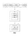
上記複合円盤アセンブリを製造する従来型プロセスが、図1のフロー図により例示される。ステップ12において、誘電性セラミック材料から円筒が形成される。ステップ14において、(未焼成又は「グリーン」の)円筒がその後、キルンの中で焼成される(一般には単に「焼成」と称される)。すなわち、セラミック材料は「焼成可能」である。ステップ16において、円筒の外表面がその後、その外径(OD)が、選択された寸法となることを確保するべく機械加工される。アセンブリ要素において精密な寸法を達成することが重要なのは、その寸法によりマイクロ波導波路の特性が影響を受けるからである。ステップ18において、円筒の内表面が、内径(ID)が、選択された寸法となることを確保するべく、同様に機械加工される。加えて、ステップ20において、磁性セラミック材料からロッドが形成される。ステップ22において、その後ロッドが焼成され、ステップ24において、その表面が、選択されたODまで機械加工される。ロッドのODは、円筒のODよりもわずかに小さいので、ロッドは、円筒の中に確実に嵌合することができる。ロッドと円筒との良好な接着を促進する密接な嵌合を達成することが理由となって、ロッドの外表面と円筒の内表面との双方が精密な公差まで機械加工される。 A conventional process for manufacturing the above composite disc assembly is illustrated by the flow diagram of FIG. In
重要なことだが、ステップ26において、エポキシ接着剤がロッド及び円筒の一方又は双方に塗布される。ステップ28において、ロッド・円筒アセンブリを形成するべくロッドが円筒の内側に挿入され、ステップ30により示されるようにエポキシの硬化(硬質化)が許容される。ステップ32において、ロッド・円筒アセンブリの外表面が再び、精密なODまで機械加工される。最後に、ステップ34においてロッド・円筒アセンブリがスライスされて一定数の円盤アセンブリとなる。すなわち、各円盤アセンブリは、誘電性セラミックリング内に同心に配置された磁性セラミック円盤を含む。各円盤アセンブリは典型的に、数ミリメートルの厚さとされる。 Importantly, in step 26, an epoxy adhesive is applied to one or both of the rod and the cylinder. At
接着を促進するための円筒内表面の機械加工、部品へのエポキシ塗布、エポキシ積載部品の慎重な取り扱い及び組み付け、並びにエポキシ硬化に関連する時間が、プロセスの非効率性に寄与してしまう。磁性・誘電性複合円盤アセンブリを製造する高効率の方法を与えることが望ましい。 The machining of the inner cylinder surface to promote adhesion, epoxy application to parts, careful handling and assembly of epoxy loaded parts, and the time associated with epoxy curing contribute to process inefficiencies. It would be desirable to provide a high efficiency method of manufacturing a magnetic and dielectric composite disc assembly.
ここに開示されるのは、無線周波数コンポーネントとして使用される複合材料の実施形態であって、ガーネット又は灰重石構造を有する低温焼成可能外側材料と、当該外側材料の中に配置された30を上回る誘電率を有する高誘電性内側材料とを含み、当該低温焼成可能外側材料及び当該高誘電性内側材料は、接着剤又はのりを使用することなく650〜900℃の温度で一緒に共焼成されるように構成される。 Disclosed herein is an embodiment of a composite material for use as a radio frequency component, comprising a low temperature calcinable outer material having a garnet or scheelite structure and more than 30 disposed in the outer material. Comprising a high dielectric inner material having a dielectric constant, the low temperature bakeable outer material and the high dielectric inner material being co-fired together at a temperature of 650-900 ° C. without using an adhesive or paste Configured as.
いくつかの実施形態において、低温焼成可能外側材料は、リングのような形状とすることができる。いくつかの実施形態において、高誘電性内側材料は、円盤のような形状とすることができる。 In some embodiments, the low temperature bakeable outer material can be shaped like a ring. In some embodiments, the high dielectric inner material can be shaped like a disk.
いくつかの実施形態において、低温焼成可能外側材料は、Na0.2Bi0.8Mo0.4V0.6O4又はNa0.35Bi0.65Mo0.7V0.3O4としてよい。In some embodiments, the low temperature calcinable outer material is Na0.2 Bi0.8 Mo0.4 V0.6 O4 or Na0.35 Bi0.65 Mo0.7 V0.3 O It may befour .
いくつかの実施形態において、低温焼成可能外側材料は、組成Bi1−2xA2xV1−xMxO4を有し得る。AはLi、Na、K、又はこれらの組み合わせであり、MはMo、W、又はこれらの組み合わせであり、xは0〜0.45である。いくつかの実施形態において、低温焼成可能外側材料は、20〜80の誘電率を有し得る。いくつかの実施形態において、低温焼成可能外側材料は、組成C2BiD2V3O12を有し得る。CはLi、Na、K、又はこれらの組み合わせであり、DはMg、Zn、Co、Ni、Cu、又はこれらの組み合わせである。いくつかの実施形態において、低温焼成可能外側材料は、BaWO4との化学式を有するタングステン酸バリウムとしてよい。In some embodiments, the low-temperature sinterable outer material may have a compositionBi 1-2x A 2x V 1-x M x O 4. A is Li, Na, K, or a combination thereof, M is Mo, W, or a combination thereof, and x is 0 to 0.45. In some embodiments, the low temperature bakeable outer material may have a dielectric constant of 20-80. In some embodiments, the low-temperature sinterable outer material may have a compositionC 2 BiD 2 V 3 O 12 . C is Li, Na, K, or a combination thereof, and D is Mg, Zn, Co, Ni, Cu, or a combination thereof. In some embodiments, the low-temperature sinterable outer material may as barium tungstate having the chemical formula of the BaWO4.
いくつかの実施形態において、タングステン酸バリウムは、MgAl2O4又はCoAl2O4により修正され得る。いくつかの実施形態において、低温焼成可能外側材料はNa2BiMg2V3O12としてよい。いくつかの実施形態において、高誘電性内側材料は約35を上回る誘電率を有してよい。In some embodiments, barium tungstate can be modified with MgAl2 O4 or CoAl2 O4 . In some embodiments, the low-temperature sinterable outer material may be aNa 2 BiMg 2 V 3 O 12 . In some embodiments, the high dielectric inner material may have a dielectric constant greater than about 35.
ここにさらに開示されるのは、無線周波数デバイスにおけるアイソレータ又はサーキュレータとして使用される複合材料を製造する方法の実施形態である。この方法は、ガーネット又は灰重石構造を有する低温焼成可能外側材料を与えることと、当該低温焼成可能外側材料の開口の中に、30を上回る誘電率を有する高誘電性内側材料を入れることと、接着剤又はのりを使用することなく当該低温焼成可能外側材料を当該高誘電性内側材料の外側表面まわりに収縮させるべく、当該低温焼成可能外側材料及び当該高誘電性内側材料を一緒に650〜900℃の温度で共焼成することとを含む。 Further disclosed herein are embodiments of a method of producing a composite material for use as an isolator or circulator in a radio frequency device. The method comprises providing a low temperature calcinable outer material having a garnet or scheelite structure, and inserting a high dielectric inner material having a dielectric constant of greater than 30 into the openings of the low temperature calcinable outer material. The low temperature bakeable outer material and the high dielectric inner material together 650-900 to shrink the low temperature bakeable outer material around the outer surface of the high dielectric inner material without the use of an adhesive or paste. Co-firing at a temperature of ° C.
いくつかの実施形態において、低温焼成可能外側材料は、組成Bi1−2xA2xV1−xMxO4を有し得る。AはLi、Na、K、又はこれらの組み合わせであり、MはMo、W、又はこれらの組み合わせであり、xは0〜0.45である。いくつかの実施形態において、低温焼成可能外側材料は、組成C2BiD2V3O12を有し得る。CはLi、Na、K、又はこれらの組み合わせであり、DはMg、Zn、Co、Ni、Cu、又はこれらの組み合わせである。いくつかの実施形態において、低温焼成可能外側材料は、化学式BaWO4を有するタングステン酸バリウムとしてよい。いくつかの実施形態において、低温焼成可能外側材料はNa2BiMg2V3O12としてよい。In some embodiments, the low-temperature sinterable outer material may have a compositionBi 1-2x A 2x V 1-x M x O 4. A is Li, Na, K, or a combination thereof, M is Mo, W, or a combination thereof, and x is 0 to 0.45. In some embodiments, the low-temperature sinterable outer material may have a compositionC 2 BiD 2 V 3 O 12 . C is Li, Na, K, or a combination thereof, and D is Mg, Zn, Co, Ni, Cu, or a combination thereof. In some embodiments, the low-temperature sinterable outer material may as barium tungstate having the formula BaWO4. In some embodiments, the low-temperature sinterable outer material may be aNa 2 BiMg 2 V 3 O 12 .
いくつかの実施形態において、方法はさらに、共焼成後の低温焼成可能外側材料及び高誘電性内側材料をスライスすることも含み得る。 In some embodiments, the method may further include slicing the co-fired low temperature calcinable outer material and the high dielectric inner material.
さらにここに開示されるのは、無線周波数アイソレータ又はサーキュレータの実施形態であって、ガーネット又は灰重石構造を有する低温焼成可能外側材料と、当該外側材料の中に配置された30を上回る誘電率を有する高誘電性内側材料とを含み、当該低温焼成可能外側材料及び当該高誘電性内側材料は、接着剤又はのりを使用することなく650〜900℃の温度で一緒に共焼成されるように構成される。 Also disclosed herein is an embodiment of a radio frequency isolator or circulator that comprises a low temperature calcinable outer material having a garnet or scheelite structure, and a dielectric constant greater than 30 disposed in the outer material. The low temperature bakeable outer material and the high dielectric inner material are configured to be co-fired together at a temperature of 650-900.degree. C. without the use of an adhesive or paste. Be done.
いくつかの実施形態において、低温焼成可能外側材料は、組成Bi1−2xA2xV1−xMxO4を有し得る。AはLi、Na、K、又はこれらの組み合わせであり、MはMo、W、又はこれらの組み合わせであり、xは0〜0.45である。いくつかの実施形態において、低温焼成可能外側材料は、組成C2BiD2V3O12を有し得る。CはLi、Na、K、又はこれらの組み合わせであり、DはMg、Zn、Co、Ni、Cu、又はこれらの組み合わせである。いくつかの実施形態において、低温焼成可能外側材料は、BaWO4との化学式を有するタングステン酸バリウムとしてよい。In some embodiments, the low-temperature sinterable outer material may have a compositionBi 1-2x A 2x V 1-x M x O 4. A is Li, Na, K, or a combination thereof, M is Mo, W, or a combination thereof, and x is 0 to 0.45. In some embodiments, the low-temperature sinterable outer material may have a compositionC 2 BiD 2 V 3 O 12 . C is Li, Na, K, or a combination thereof, and D is Mg, Zn, Co, Ni, Cu, or a combination thereof. In some embodiments, the low-temperature sinterable outer material may as barium tungstate having the chemical formula of the BaWO4.
ここに開示されるのは、低焼成の誘電性材料の複数の実施形態である。これらの材料は、アイソレータ及びサーキュレータのアプリケーションのような磁性・誘電性アセンブリのための複合体を形成するべく、高誘電性材料とともに共焼成することができる。有利なことに、開示の材料の実施形態は、のり、エポキシ又は他の化学接着剤のようないずれの接着剤も必要とすることなく共焼成することができる。すなわち、本開示の実施形態から形成される複合物は、のりなし、エポキシなし、化学的付着なし、又は接着剤なしとすることができる。すなわち、いくつかの実施形態において、複合アセンブリを形成するときに、のり、エポキシ、及び接着剤が使用されることがない。 Disclosed herein are multiple embodiments of low firing dielectric materials. These materials can be co-fired with high dielectric materials to form composites for magnetic and dielectric assemblies such as isolator and circulator applications. Advantageously, embodiments of the disclosed material can be co-fired without the need for any adhesive such as paste, epoxy or other chemical adhesive. That is, the composites formed from the embodiments of the present disclosure can be without glue, without epoxy, without chemical attachment, or without adhesive. That is, in some embodiments, glue, epoxy, and adhesives are not used when forming the composite assembly.
本開示の実施形態によれば、有利なことに、詳しくは3GHz及びこれを上回る周波数で動作する5Gシステムが、アンテナ、サーキュレータ、増幅器、及び/又は半導体ベースの増幅器のような異なるコンポーネントを含み得る統合アーキテクチャを形成することが可能となる。これらのコンポーネントの単一基板への統合が許容されることにより、デバイスの全体的な小型化を進めることができる。いくつかの実施形態において、開示のデバイスは、約1.8GHzから約30GHzの周波数で動作可能とすることができる。いくつかの実施形態において、開示のデバイスは、約1、2、3、4、5、10、15、20又は25GHz超過の周波数で動作可能とすることができる。いくつかの実施形態において、開示のデバイスは、30、25、20、15、10、5、4、3又は2GHz未満の周波数で動作可能とすることができる。 According to embodiments of the present disclosure, advantageously, 5G systems operating at 3 GHz and above may in particular include different components such as antennas, circulators, amplifiers and / or semiconductor based amplifiers. It is possible to form an integrated architecture. Allowing integration of these components on a single substrate can facilitate the overall miniaturization of the device. In some embodiments, the disclosed devices can be operable at a frequency of about 1.8 GHz to about 30 GHz. In some embodiments, the disclosed devices can be operable at frequencies above about 1, 2, 3, 4, 5, 10, 15, 20 or 25 GHz. In some embodiments, the disclosed devices can be operable at frequencies less than 30, 25, 20, 15, 10, 5, 4, 3 or 2 GHz.
いくつかの実施形態において、統合アーキテクチャは、標準的なアイソレータよりもそれほど大きくないパッケージサイズの方向性結合器及び/又はアイソレータを含み得る。いくつかの実施形態において、統合アーキテクチャは高電力スイッチを含み得る。誘電性タイルをインピーダンス変換器用の基板として使用することに加え、誘電性タイルはまた、結合器、スイッチ及び終端用の基板としても使用することができる。 In some embodiments, the integrated architecture may include directional couplers and / or isolators of package sizes not much larger than standard isolators. In some embodiments, the integrated architecture may include a high power switch. In addition to using dielectric tiles as a substrate for impedance converters, dielectric tiles can also be used as substrates for couplers, switches and terminations.
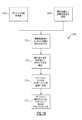
図2は、一以上の化学元素(ブロック1)、化学複合物(ブロック2)、化学物質(ブロック3)及び/又は化学混合物(ブロック4)を、ここに記載の一以上の特徴を有する一以上の材料(ブロック5)を得るべくどのようにして処理することができるのかを模式的に示す。いくつかの実施形態において、かかる材料は、所望の誘電特性(ブロック7)、磁気特性(ブロック8)を含むように構成されたセラミック材料(ブロック6)にすることができる。 Figure 2 shows one or more chemical elements (block 1), chemical compounds (block 2), chemicals (block 3) and / or chemical mixtures (block 4) having one or more of the features described herein It schematically shows how it can be processed to obtain the above material (block 5). In some embodiments, such material can be a ceramic material (block 6) configured to include the desired dielectric properties (block 7) and magnetic properties (block 8).
いくつかの実施形態において、上記特性の一以上を有する材料を、無線周波数(RF)アプリケーションのようなアプリケーション(ブロック10)に実装することができる。かかるアプリケーションは、デバイス12においてここに記載の一以上の特徴を含み得る。いくつかのアプリケーションにおいて、かかるデバイスはさらに、製品11に実装することができる。かかるデバイス及び/又は製品の例がここに記載される。 In some embodiments, materials having one or more of the above characteristics can be implemented in an application (block 10), such as a radio frequency (RF) application. Such applications may include one or more of the features described herein at
マイクロストリップサーキュレータ/アイソレータ Microstrip circulator / isolator
サーキュレータは、マイクロ波又は無線周波数(RF)のような異なる信号を送受信できる受動マルチポートデバイスである。当該ポートは、サーキュレータへと又はサーキュレータから接続される外部導波路又は伝送線路とすることができる。アイソレータは、サーキュレータに類似するが、当該ポートの一以上が遮断され得る。それゆえ、サーキュレータとアイソレータとは、一般的な構造が類似し得ることからここでは、互換可能に使用することができる。よって、以下の説明はすべて、サーキュレータ及びアイソレータの双方に当てはまる。 A circulator is a passive multiport device that can transmit and receive different signals such as microwave or radio frequency (RF). The port can be an external waveguide or transmission line connected to or from the circulator. The isolator is similar to a circulator but one or more of the ports can be shut off. Therefore, circulators and isolators can be used interchangeably as they have similar general structures. Thus, all the following description applies to both circulators and isolators.
マイクロストリップサーキュレータ及びアイソレータは、業界で知られるデバイスであり、誘電性フェライト基板のような基板を覆うように堆積された薄膜回路からなる。いくつかの実施形態において、一以上のフェライト円盤を当該基板に接着することができる。その後さらに、フェライト円盤を通る信号を循環させるべく磁石が付着される。 Microstrip circulators and isolators are devices known in the art and consist of thin film circuits deposited over a substrate such as a dielectric ferrite substrate. In some embodiments, one or more ferrite disks can be bonded to the substrate. Thereafter, a magnet is attached to circulate the signal through the ferrite disk.
さらに、全フェライトのマイクロストリップサーキュレータもまた、詳しくはT/Rモジュール用として、使用されている。全フェライトのマイクロストリップサーキュレータに回路群をプリントすることができ、頂部に、信号を誘導する磁石を加えることができる。例えば、フェライト基板上にメタライゼーションパターンが形成される。典型的に、メタライゼーションパターンは、中心円盤及び多数の伝送線路からなる。 Furthermore, all ferrite microstrip circulators are also used, in particular for T / R modules. Circuit groups can be printed on the whole ferrite microstrip circulator and a signal inducing magnet can be added on top. For example, a metallization pattern is formed on a ferrite substrate. Typically, the metallization pattern consists of a central disk and a number of transmission lines.
サーキュレータは一般に、共鳴動作領域の上側又は下側のいずれかで動作することができる。これが図3に示される。いくつかの実施形態において、上側共鳴周波数は、狭帯域のサブ4GHzサーキュレータにとって有利となり得る。それよりも高い周波数に対しては、下側共鳴領域が有利となり得る。 The circulator can generally operate either above or below the resonant operating region. This is shown in FIG. In some embodiments, the upper resonance frequency may be advantageous for a narrow band sub-4 GHz circulator. For higher frequencies, the lower resonance region may be advantageous.
マイクロストリップサーキュレータは詳しくは、下側共鳴動作領域において動作するのが典型的である。当該サーキュレータは、例えば六角形フェライトの場合には非常に小さい磁石を使用する。すなわち自己バイアスがかかり得る。しかしながら、正方形タイルは、詳しくは業界で知られる全フェライトマイクロストリップサーキュレータにとって、均一に磁化することが難しい形状である。すなわち、これらは、低磁場損失領域近くで動作する。変換器が高損失の未磁化フェライト上に取り付けられると、性能が損なわれる。さらに、電力が増加すると、性能の悪化がさらに知られるようになる。したがって、業界で知られるサーキュレータは、性能損失及び相互変調ひずみ(IMD)並びに電力性能の悪化につながるフェライトタイルの不良な磁化に起因する問題に悩まされる。 The microstrip circulator typically operates in the lower resonance operating region. The circulator uses very small magnets, for example in the case of hexagonal ferrites. That is, it can be self-biased. However, square tiles are shapes that are difficult to magnetize uniformly, particularly for all ferrite microstrip circulators known in the art. That is, they operate near the low field loss region. Performance is compromised if the transducer is mounted on high loss unmagnetized ferrite. Furthermore, as power increases, performance degradation becomes more known. Thus, circulators known in the art suffer from problems due to poor magnetization of ferrite tiles leading to loss of performance and intermodulation distortion (IMD) and degradation of power performance.
共焼成マイクロストリップサーキュレータ/アイソレータ Co-fired microstrip circulator / isolator
本開示の実施形態によれば、全体的な磁化が改善され、現在知られているマイクロストリップサーキュレータに生じ得る性能問題を低減することができる。一般に、マイクロストリップサーキュレータは、例えばイットリウム鉄ガーネット(YIG)から作られた酸化物フェライト円盤のようなフェライト円盤を、誘電性基板に直接組み込むことによって形成することができる。その組み合わせがその後、共焼成されて硬い複合構造が形成される。銀又は他のメタライゼーション物質から形成された付加回路群を加えることができる。共焼成プロセスがなければ、回路メタライゼーションを適用することができない。本開示の実施形態により、業界の有意な問題のいくつかを軽減することができる。 According to embodiments of the present disclosure, the overall magnetization may be improved to reduce performance problems that may occur with currently known microstrip circulators. In general, microstrip circulators can be formed by incorporating directly into the dielectric substrate a ferrite disc, such as an oxide ferrite disc made of, for example, yttrium iron garnet (YIG). The combination is then co-fired to form a hard composite structure. Additional circuits formed from silver or other metallization material can be added. Without the co-firing process, circuit metallization can not be applied. Embodiments of the present disclosure can alleviate some of the significant problems in the industry.
任意数の異なるフェライト円盤材料を使用することができる。いくつかの実施形態において、フェライト円盤材料の飽和磁化レベルは、1000〜5000(又は約1000〜約5000)ガウスの範囲となり得る。 Any number of different ferrite disc materials can be used. In some embodiments, the saturation magnetization level of the ferrite disk material can be in the range of 1000 to 5000 (or about 1000 to about 5000) gauss.
さらに、業界で知られる任意数の異なる誘電性基板も使用することができる。さらに、誘電体は、誘電性粉末又は低温共焼成セラミック(LTCC)テープから形成することができる。いくつかの実施形態において、誘電率は、6、10、15、20、25、30、40、50又は60を上回るようにすることができる。いくつかの実施形態において、誘電率は、6〜30(又は約6から約30)からの範囲となり得る。いくつかの実施形態において、誘電率は、約60、50、40、30、25、20、15又は10を下回るようにすることができる。 Additionally, any number of different dielectric substrates known in the art can also be used. Additionally, the dielectric can be formed from dielectric powder or low temperature co-fired ceramic (LTCC) tape. In some embodiments, the dielectric constant can be greater than 6, 10, 15, 20, 25, 30, 40, 50 or 60. In some embodiments, the dielectric constant can range from 6 to 30 (or about 6 to about 30). In some embodiments, the dielectric constant can be less than about 60, 50, 40, 30, 25, 20, 15 or 10.
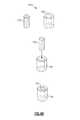
詳しくは、図4A〜4Bに示されるように、複合マイクロストリップサーキュレータ100を形成するべく、磁性酸化物円盤102又は他の磁性円盤を誘電性基板104の開口に挿入することができる。いくつかの実施形態において、円盤102は、円筒状ロッドとなり得る。ただし、この特定の形状に制限されるわけではない。円盤102は、グリーンでも、事前焼成でも、非事前焼成でもよい。 In particular, as shown in FIGS. 4A-4B, a
さらに、基板104は一般に、図4Aに示されるように矩形柱でよいが、図4Bに示される円筒のような他の形状も同様に使用することができる。基板104の実施形態は、以下に詳細に開示される。ひとたび円盤102が基板104の内部に存在すれば、特許文献1又は2に説明される方法を使用してコンポーネントを一緒に焼成(例えば共焼成)することができる。特許文献1又は2は、その全体がここに参照により組み入れられて以下に説明される。この共焼成プロセスにより、さらに以下に詳述されるように、基板104は、円盤102まわりに収縮し、これを、複合構造100を形成するべく接着剤を伴って一定位置に保持することができる。この複合構造物100はその後スライスされ、図5A〜5Bに示されるチップ構造物を形成する(図5Aが矩形柱スライスを示し、図5Bが円筒スライスを示す)。しかしながら、いくつかの実施形態において、スライスは行われず、当該コンポーネントが最終厚さにおいて一緒に共焼成される。いくつかの実施形態において、複数の異なる円盤を、複数の異なる開口において単一の基板の中に挿入することができる。 Furthermore, the
このように、いくつかの実施形態において、磁性酸化物円盤を共焼成して、正方形若しくは矩形の誘電性基板又は任意の他形状の基板にすることができる。当該基板はその後、回路群のような他のコンポーネントのためのプラットフォームとしての役割を果たすことができる。この複合構造物はその後、磁石されて例えばマイクロストリップサーキュレータ及び/又はアイソレータパッケージとしての役割を果たすことができる。または、フェライト円盤は、挿入前に磁化しておくこともできる。いくつかの実施形態において、フェライト円盤は、共焼成ステップに先立って磁化することができる。 Thus, in some embodiments, the magnetic oxide disk can be co-fired into a square or rectangular dielectric substrate or a substrate of any other shape. The substrate can then serve as a platform for other components, such as circuits. The composite structure can then be magnetized to serve, for example, as a microstrip circulator and / or an isolator package. Alternatively, the ferrite disk can be magnetized prior to insertion. In some embodiments, the ferrite disk can be magnetized prior to the co-firing step.
ひとたび複合構造物が形成されると、当該基板に、付加薄膜回路等のような他のコンポーネントを加えることができる。このように、本開示の実施形態は、標準的なアイソレータよりもそれほど大きくはないパッケージサイズの方向性結合器及び/又はアイソレータを含み得る統合ソリューションを形成することができる。さらに、有利なことに損失は、当該レベルの磁場によっては影響を受けず、又は少なくとも低減され得る。いくつかの実施形態において、開示のサーキュレータは、すべての現行のフェライトマイクロストリップサーキュレータよりも大きくなることがない(さらに、選択されたフェライト/誘電体の組み合わせに応じて小さくなりえる)。 Once the composite structure is formed, other components can be added to the substrate, such as additional thin film circuits and the like. Thus, embodiments of the present disclosure can form an integrated solution that may include directional couplers and / or isolators of package size not much larger than standard isolators. Furthermore, advantageously, the losses can be unaffected or at least reduced by the level of the magnetic field. In some embodiments, the disclosed circulators can not be larger than all current ferrite microstrip circulators (and can be smaller depending on the selected ferrite / dielectric combination).
このように、共焼成プロセスを使用して、図5A〜5Bに示されるように、フェライト円盤を誘電性タイルに組み入れることができる。図に示される薄いフェライト円盤は、業界で知られる正方形又は他の奇妙な形状の小片よりもはるかに容易に、均一に磁化することができる。いくつかの実施形態において、誘電性タイルは、約25mm正方形となり得る。ただし、この特定の寸法に限られるわけではない。これは、3〜4(又は約3〜約4)GHzの領域において使用することができる。 Thus, a co-firing process can be used to incorporate ferrite disks into dielectric tiles, as shown in FIGS. 5A-5B. The thin ferrite disks shown in the figure can be uniformly magnetized much more easily than square or other odd shaped pieces known in the art. In some embodiments, the dielectric tile can be about 25 mm square. However, it is not necessarily limited to this specific dimension. This can be used in the region of 3-4 (or about 3 to about 4) GHz.
誘電性タイルを使用してその後、図6に示されるような変換器を製造することができる。図示のように、基板104は、他のコンポーネントアタッチメントのために空けられたスペースを有する。変換器の形成後、図7に示されるように、小さな磁石のみを当該タイル上に配置しなければならない。すなわち、組み付け時間を、従前に行われていたよりもかなり短くすることができる。 The dielectric tile can then be used to produce a transducer as shown in FIG. As shown, the
誘電性タイルは、インピーダンス変換器用の基板として使用することに加え、結合器、スイッチ、終端のための基板としても使用することができる。すなわち、デバイスの全体的な設置面積を低減する共焼成後に、一定数の他のコンポーネントを当該基板上に加えることができる。さらに、回路メタライゼーションも加え得るが、これはデバイスが共焼成された後に限られる。 In addition to being used as a substrate for impedance converters, dielectric tiles can also be used as substrates for couplers, switches, terminations. That is, after co-firing to reduce the overall footprint of the device, a number of other components can be added onto the substrate. In addition, circuit metallization may also be added, but only after the device has been co-fired.
リング用の低温焼成誘電性材料 Low temperature fired dielectric material for rings
本開示の実施形態は、例えば、アンテナのような無線周波数コンポーネント用のサーキュレータ/アイソレータの形成を目的とした、磁性材料を使用した共焼成プロセスにとって特に有利となり得る。詳しくは、磁性材料を、低い焼成温度により高誘電性磁性材料とすることができる(例えば低温で焼成可能とすることができる)。 Embodiments of the present disclosure may be particularly advantageous for co-firing processes using magnetic materials, for example for the purpose of forming circulators / isolators for radio frequency components such as antennas. In particular, the magnetic material can be made into a high dielectric magnetic material (eg, be able to be fired at low temperatures) with a low firing temperature.
具体的には、上記図4A〜4Bに示されるような開示の低温焼成誘電性材料の実施形態から形成された未焼成リングに(104がリングであり、102がロッドである)、磁性材料のロッド(又は円盤若しくは正方形のような他の形状)を挿入することができる。リングとロッドとの組み合わせはその後、一緒に共焼成され、当該リングが当該ロッドまわりに収縮する。これらの材料は双方とも、「焼成可能」とすることができる。「焼成可能」とは、これらが、オーブン/キルン/他の加熱デバイスにおいて焼成又は焼結され得ることを意味する。いくつかの実施形態において、焼成により、ここで説明されるセラミック材料のような材料の一以上の特性が変化し得る。すなわち、リング材料及びロッド材料が、これらの物理特性のいずれかへのマイナスの影響を回避するべく一般に類似する焼成温度を有することが、有利となり得る。これらのアセンブリの実施形態は、5Gアプリケーションのような無線周波数アプリケーションのためのアイソレータ及び/又はサーキュレータとして使用することができる。 Specifically, a green ring (104 is a ring and 102 is a rod) formed of an embodiment of the disclosed low temperature fired dielectric material as shown in FIGS. 4A-4B above (104 being a ring and 102 being a rod) A rod (or other shape such as a disc or square) can be inserted. The combination of ring and rod is then co-fired together and the ring shrinks around the rod. Both of these materials can be "sinterable". By "bakable" is meant that they can be fired or sintered in an oven / kiln / other heating device. In some embodiments, firing can change one or more properties of a material such as the ceramic material described herein. That is, it may be advantageous for the ring and rod materials to have generally similar firing temperatures to avoid negative effects on any of these physical properties. Embodiments of these assemblies can be used as isolators and / or circulators for radio frequency applications such as 5G applications.
有利なことに、この共焼成プロセスは、接着剤/エポキシ/のりなしで行うことができるので、「のりなしアセンブリ」又は「接着剤なしアセンブリ」とみなすことができる。リング焼成温度が高すぎると、溶融をもたらし、又は少なくとも内部ロッドの特性をかなり損なわせ得るが、それゆえ、組み付けの従前の反復は、焼成可能リングを焼成可能ロッドとは別に焼成する。先行技術の方法に対しては、双方のセグメントが別々に焼成され得る。または、リングを最初に焼成し、その後、リング/ロッドアセンブリが一緒に焼成される。これらのアプローチはいずれも、リングがロッドまわりに十分に収縮するわけではなく、ひいては、リング及びロッドが互いに付着し合うように接着剤又は他の化学的付着手段が必要とされる。このため、本開示の実施形態は、いずれの接着剤も使用することなく磁性ロッドまわりに収縮するリング材料とすることができる。これは、リングをロッドまわりに収縮させることの(摩擦力のような)機械的拘束となって、当該ロッドを当該リング内の一定位置に保持する。 Advantageously, this co-firing process can be considered as a "glue free assembly" or a "glue free assembly" since it can be performed without an adhesive / epoxy / glue. If the ring firing temperature is too high, it can lead to melting or at least considerable loss of the properties of the inner rod, so the previous iteration of the assembly fires the bakeable ring separately from the bakeable rod. For prior art methods, both segments can be fired separately. Alternatively, the ring is fired first, and then the ring / rod assembly is fired together. None of these approaches cause the ring to shrink sufficiently around the rod, which in turn requires an adhesive or other chemical attachment means so that the ring and rod adhere to one another. Thus, embodiments of the present disclosure can be ring materials that shrink around the magnetic rod without using any adhesive. This provides a mechanical constraint (such as friction) on the contraction of the ring about the rod to hold the rod in place within the ring.
接着剤は一定数の欠点を有するので、開示の接着剤なしアセンブリを使用することは有利となり得る。有利なことに、開示の材料は、ロッド及びリングが一緒に共焼成され得るので、そのような接着剤を必要とすることなしに複合構造を形成し得る。例えば、ひとたび接着剤が存在すると、アセンブリのメタライゼーションは、不可能ではないにしても極めて難しい。これは、メタライゼーションに必要とされる温度が、接着剤のための使用温度よりもかなり高くなり、当該接着剤が溶融及び/又は接着剤喪失をもたらすからである。さらに、接着剤が喪失されると、のり付けされたコンポーネントの性能損失が増加する。高周波数におけるのり/接着剤の誘電性損失は、磁性又は誘電性材料よりも大きい。すなわち、有利なことに、開示のアセンブリは接着剤の使用を必要としない。 As adhesives have a certain number of drawbacks, it may be advantageous to use the disclosed adhesiveless assembly. Advantageously, the disclosed materials can form a composite structure without the need for such an adhesive since the rods and rings can be co-fired together. For example, once the adhesive is present, metallization of the assembly is extremely difficult if not impossible. This is because the temperature required for the metallization is considerably higher than the use temperature for the adhesive, which leads to melting and / or adhesive loss. Furthermore, the loss of adhesive increases the performance loss of glued components. The dielectric loss of pastes / adhesives at high frequencies is greater than magnetic or dielectric materials. That is, advantageously, the disclosed assembly does not require the use of an adhesive.
リング内に保持される磁性ロッドとして、以下の材料を使用することができる。具体的には、リング材料の実施形態は、全体がここに参照により組み入れられる特許文献3に開示のように、高磁化スピネル(例えばニッケル亜鉛フェライト)ロッドとの共焼成に適した、詳しくは高周波数(5G)アプリケーションに適した、低い誘電率(10未満)を有し得る。これは、Ni1−w−x−y−zZnwCoxMnyCuzFe2O4のような材料を含み得る。ここで、wは0.2から0.6の範囲であり、x、y及びzはそれぞれが0から0.2の範囲であり、aは0から0.2の範囲である。好ましい実装において、w=0.4725、x=0.0225、y=0.02、z=0、かつa=0.08である。他の好ましい実装において、w=0.4、x=0.0275、y=0.01、z=0、かつa=0.08である。一つの実装において、ロッド材料は、式Ni1−x−yZnxCoyFe2O4により代表され得る。ここで、x=0.2〜0.6、及び0<y<0.2である。The following materials can be used as the magnetic rod held in the ring. Specifically, embodiments of the ring material are suitable for co-firing with highly magnetized spinel (e.g. nickel zinc ferrite) rods, as disclosed in U.S. Pat. It may have a low dielectric constant (less than 10) suitable for frequency (5G) applications. Thismay include materials such asNi 1-w-x-y -z Zn w Co x Mn y Cu z Fe 2 O 4. Here, w is in the range of 0.2 to 0.6, x, y and z are each in the range of 0 to 0.2, and a is in the range of 0 to 0.2. In a preferred implementation, w = 0.4725, x = 0.0225, y = 0.02, z = 0, and a = 0.08. In another preferred implementation, w = 0.4, x = 0.0275, y = 0.01, z = 0, and a = 0.08. In one implementation, the rod material can be represented by the formulaNi 1-x-y Zn x Co y Fe 2 O 4. Here, x = 0.2 to 0.6 and 0 <y <0.2.
さらに、リング内に保持される磁性ロッドとして、以下の材料も使用することができる。すなわち、開示の低焼成誘電性リング材料の実施形態は、全体がここに参照により組み入れられる特許文献4に開示のように、高誘電率ロッド材料との共焼成が可能な灰重石又はガーネット構造を有し得る。高誘電率磁性ロッドは、ビスマス置換高誘電率磁性ガーネットとしてよい。開示の全体がここに参照により組み入れられる「インジウム含有磁性ガーネット材料」との名称で2018年5月7日に出願された米国特許出願第15/972,617号明細書に開示のような他の材料も使用することができる。ガーネットの例は、Y3−x−yBixCayZryFe5−yO12を含む。いくつかの実施形態において、0<x<1.8かつ0<y<1.0である。いくつかの実施形態において、修正された合成ガーネット組成を、一般組成Y3−x−y−2aBixCay+2aZryInzVaFe5−y−z−aO12により定義することができる。いくつかの実施形態において、0<x<1.8、0<y<1.0、0<z <1.0、かつ0<a<1.0である。In addition, the following materials can also be used as magnetic rods held in the ring. That is, embodiments of the disclosed low-fired dielectric ring material, as disclosed in U.S. Pat. No. 5,959,059, which is incorporated herein by reference in its entirety, has an ashite or garnet structure capable of co-firing with a high permittivity rod material It can have. The high dielectric constant magnetic rod may be a bismuth-substituted high dielectric constant magnetic garnet. Other disclosures as disclosed in US Patent Application No. 15 / 972,617, filed May 7, 2018, entitled "Indium-Containing Magnetic Garnet Material", the entire disclosure of which is incorporated herein by reference. Materials can also be used. Examples ofgarnets, includingY 3-x-y Bi x Ca y Zr y Fe 5-
磁性ロッド材料に関して上に与えられた例は、単なる例であって、他の材料も同様に使用することができる。いくつかの実施形態において、磁性ロッド材料(例えば高誘電性内側材料)は、約20、30、35、40又は50の誘電率を有し得る。いくつかの実施形態において、磁性ロッド材料は、60、50又は40を下回る誘電率を有し得る。 The examples given above for the magnetic rod material are merely examples, and other materials can be used as well. In some embodiments, the magnetic rod material (eg, a high dielectric inner material) may have a dielectric constant of about 20, 30, 35, 40 or 50. In some embodiments, the magnetic rod material may have a dielectric constant less than 60, 50 or 40.
上述のように、化学接着剤の使用を回避するべく、上述の磁性ロッド材料のような高磁性ロッド材料と両立する(例えば焼成/焼結温度が両立する)外側リング材料を使用することは、有利となり得る。 As mentioned above, to avoid the use of chemical adhesives, it is possible to use an outer ring material compatible with the high magnetic rod material such as the magnetic rod material described above (eg compatible with the firing / sintering temperature) It can be advantageous.
いくつかの実施形態において、焼成可能リング材料(例えば低温焼成誘電性材料)は、化学式BiVO4を有するバナジウム酸ビスマスに基づき得る。例えば、当該材料の実施形態は、一般式Bi1−2xA2xV1−xMxO4を有し得る。いくつかの実施形態において、xは0〜0.45(又は約0〜約0.45)となり得る。いくつかの実施形態において、0<x<0.45である。いくつかの実施形態において、xは0.45と等しくなり得る。Aは、Li、Na、K、又はこれらの組み合わせとなり得る。Mは、Mo、W、又はこれらの組み合わせとなり得る。In some embodiments, the bakeable ring material (eg, a low temperature fired dielectric material) can be based on bismuth vanadate having the formula BiVO4 . For example, embodiments of the material may have the general formulaBi 1-2x A 2x V 1-x M x O 4. In some embodiments, x can be from 0 to 0.45 (or about 0 to about 0.45). In some embodiments, 0 <x <0.45. In some embodiments, x may be equal to 0.45. A can be Li, Na, K, or a combination thereof. M can be Mo, W, or a combination thereof.
このリング材料は、900℃を下回る焼結温度、詳しくは650〜800℃の焼結温度(例えば焼成温度)を有し得る。いくつかの実施形態において、材料は、850℃を下回る焼結温度となり得る。いくつかの実施形態において、材料は、900、850、800又は750℃を下回る(又は約900、約850、約800若しくは約750℃を下回る)焼結温度を有し得る。いくつかの実施形態において、材料は、500、550、600、650又は700℃を上回る(又は約500、約550、約600、約650若しくは約750℃を上回る)焼結温度を有し得る。 The ring material may have a sintering temperature below 900 ° C., specifically a sintering temperature (eg, a firing temperature) of 650-800 ° C. In some embodiments, the material can have a sintering temperature below 850 ° C. In some embodiments, the material can have a sintering temperature below 900, 850, 800 or 750 ° C. (or below about 900, about 850, about 800 or about 750 ° C.). In some embodiments, the material can have a sintering temperature above 500, 550, 600, 650 or 700 ° C. (or above about 500, about 550, about 600, about 650 or about 750 ° C.).
さらに、リング材料の実施形態は、20〜80(又は約20〜約80)又は20〜70(又は約20〜約70)の誘電率範囲を有し得る。いくつかの実施形態において、材料は、10、20、30、40、50、60又は70を上回る(又は約10、20、30、40、50、60若しくは70を上回る)誘電率を有し得る。いくつかの実施形態において、材料は、80、70、60、50、40、30又は20を下回る(又は約80、70、60、50、40、30若しくは20を下回る)誘電率を有し得る。 Furthermore, embodiments of the ring material may have a dielectric constant range of 20-80 (or about 20 to about 80) or 20 to 70 (or about 20 to about 70). In some embodiments, the material may have a dielectric constant greater than 10, 20, 30, 40, 50, 60 or 70 (or more than about 10, 20, 30, 40, 50, 60 or 70) . In some embodiments, the material may have a dielectric constant less than (or less than about 80, 70, 60, 50, 40, 30 or 20) 80, 70, 60, 50, 40, 30 or 20 .
代替実施形態において、リング材料は、組成C2BiD2V3O12を有し得る。Cは、Li、Na、K、又はこれらの組み合わせとなり得る。Dは、Mg、Zn、Co、Ni、Cu、又はこれらの組み合わせとなり得る。この組成はガーネット構造を有し得る。In an alternative embodiment, the ring material may have a compositionC 2 BiD 2 V 3 O 12 . C can be Li, Na, K, or a combination thereof. D can be Mg, Zn, Co, Ni, Cu, or a combination thereof. This composition may have a garnet structure.
このリング材料は、900℃を下回る焼結温度、詳しくは650〜800℃の焼結温度を有し得る。いくつかの実施形態において、材料は、850℃を下回る焼結温度となり得る。いくつかの実施形態において、材料は、900、850、800又は750℃を下回る(又は約900、約850、約800若しくは約750℃を下回る)焼結温度を有し得る。いくつかの実施形態において、材料は、500、550、600、650又は700℃を上回る(又は約500、約550、約600、約650若しくは約750℃を上回る)焼結温度を有し得る。 The ring material may have a sintering temperature below 900 ° C., in particular a sintering temperature of 650-800 ° C. In some embodiments, the material can have a sintering temperature below 850 ° C. In some embodiments, the material can have a sintering temperature below 900, 850, 800 or 750 ° C. (or below about 900, about 850, about 800 or about 750 ° C.). In some embodiments, the material can have a sintering temperature above 500, 550, 600, 650 or 700 ° C. (or above about 500, about 550, about 600, about 650 or about 750 ° C.).
さらに、リング材料の実施形態は、10〜30(又は約10〜約30)の誘電率範囲を有し得る。いくつかの実施形態において、材料は、10、15、20、25又は30を上回る(又は約10、15、20、25若しくは30を上回る)誘電率を有し得る。いくつかの実施形態において、材料は、30、25、20、15又は10を下回る(又は約30、25、20、15若しくは10を下回る)誘電率を有し得る。 Furthermore, embodiments of the ring material may have a dielectric constant range of 10 to 30 (or about 10 to about 30). In some embodiments, the material can have a dielectric constant greater than 10, 15, 20, 25 or 30 (or greater than about 10, 15, 20, 25 or 30). In some embodiments, the material can have a dielectric constant less than 30, 25, 20, 15 or 10 (or less than about 30, 25, 20, 15 or 10).
代替実施形態において、リング材料はNa2BiMg2V3O12としてよい。この材料は、25(又は約25)の誘電率を有し得る。In an alternative embodiment, the ring material may be aNa 2 BiMg 2 V 3 O 12 . This material may have a dielectric constant of 25 (or about 25).
この材料は、900℃を下回る焼結温度、詳しくは650〜800℃の焼結温度を有し得る。いくつかの実施形態において、材料は、850℃を下回る焼結温度を有し得る。いくつかの実施形態において、材料は、900、850、800又は750℃を下回る(又は約900、約850、約800若しくは約750℃を下回る)焼結温度を有し得る。いくつかの実施形態において、材料は、500、550、600、650又は700℃を上回る(又は約500、約550、約600、約650若しくは約750℃を上回る)焼結温度を有し得る。 This material may have a sintering temperature below 900 ° C., in particular a sintering temperature of 650-800 ° C. In some embodiments, the material can have a sintering temperature below 850 ° C. In some embodiments, the material can have a sintering temperature below 900, 850, 800 or 750 ° C. (or below about 900, about 850, about 800 or about 750 ° C.). In some embodiments, the material can have a sintering temperature above 500, 550, 600, 650 or 700 ° C. (or above about 500, about 550, about 600, about 650 or about 750 ° C.).
いくつかの実施形態において、結合剤を、上記開示のリング材料組成の中にブレンドしてよい。例えば、結合剤は、ポリビニルアルコール(PVA)又はポリエチレングリコール(PEG)の単独又は組み合わせとなり得る。しかしながら、結合剤のタイプは限られるわけではない。例えば、結合剤は、組成全体の2%レベルとして導入してよい。 In some embodiments, a binder may be blended into the ring material composition disclosed above. For example, the binder can be polyvinyl alcohol (PVA) or polyethylene glycol (PEG) alone or in combination. However, the type of binder is not limited. For example, the binder may be introduced as a 2% level of the overall composition.
以下の表Iは、有利なことに外側リング材料として使用することができる一定数の材料の焼成温度及び誘電率を与える。すなわち、いくつかの実施形態において、外側リング材料は灰重石構造を有し得る。
いくつかの実施形態において、タングステン酸バリウムは、外側リングのための低温焼成誘電性材料として使用することができる。タングステン酸バリウムは、式BaWO4を有して灰重石構造を形成することができる。さらに、タングステン酸バリウムを主要成分として備えた固溶体も使用することができる。これは詳しくは、上述のような、リチウムフェライト又はニッケル亜鉛フェライトのような高磁化スピネルとともに焼成する低誘電率共焼成可能材料として使用することができる。この材料を使用することは、モーディングを回避する上で、及び高周波数においても必要な薄い基板のインピーダンス効果をオフセットする上で、有利となり得る。In some embodiments, barium tungstate can be used as a low temperature fired dielectric material for the outer ring. Barium tungstate can have the formula BaWO4 to form a scheelite structure. Furthermore, a solid solution having barium tungstate as a main component can also be used. It can be used in particular as a low dielectric co-fireable material fired with highly magnetized spinels such as lithium ferrite or nickel zinc ferrite as described above. The use of this material can be advantageous in avoiding modalities and in offsetting the thin substrate impedance effects necessary even at high frequencies.
これは、高周波マイクロストリップ又は表面統合導波路設計にとって特に有用となり得る。 This can be particularly useful for high frequency microstrip or surface integrated waveguide designs.
いくつかの実施形態において、タングステン酸バリウムは、フェライトの熱膨張性を修正するべくMgAl2O4又はCoAl2O4によって修正することができる。しかしながら、この修正もまた、上述のようなリング材料のいずれかによって行うことができる。例えば、これらの組成は、上述のような外側リング材料の焼結に先立って混合することができる。フェライト外側リングの熱膨張が、誘電性磁性ロッドに密接に整合することは有利となり得る。In some embodiments, barium tungstate can be modified with MgAl2 O4 or CoAl2 O4 to modify the thermal expansion of the ferrite. However, this modification can also be done by any of the ring materials as described above. For example, these compositions can be mixed prior to sintering of the outer ring material as described above. It may be advantageous for the thermal expansion of the ferrite outer ring to be closely matched to the dielectric magnetic rod.
以下の表IIは、外側リング材料として有利な材料の例、及びその固有特性を示す。
いくつかの実施形態において、上に開示のリング材料は、10未満(又は約10未満)のε’を有し得る。すなわち、本開示の実施形態は、5Gを下回る共鳴アプリケーションのために使用することができる。これは、モーディングを回避する上で、及び高周波数でも使用される薄い基板のインピーダンス効果をオフセットする上で、有利となり得る。したがって、10を下回る(又は約10を下回る)値が、20GHzを上回る周波数に対して使用される。 In some embodiments, the ring material disclosed above can have an ε 'of less than 10 (or less than about 10). That is, embodiments of the present disclosure can be used for resonance applications below 5G. This can be advantageous in avoiding moding and in offsetting the impedance effects of thin substrates used even at high frequencies. Thus, values below 10 (or below about 10) are used for frequencies above 20 GHz.
5Gアプリケーション 5G application
開示の複合マイクロストリップサーキュレータの実施形態は、第5世代無線システム(5G)アプリケーションにとって特に有利となり得る。ただし、初期の4G及び3Gアプリケーションに対しても使用することができる。5G技術はまた、ここでは5Gニューラジオ(NR)とも称される。5Gネットワークは、一エリアに多数の消費者を許容することができる現行の4Gシステムよりも有意に高い容量を与えることができる。これはさらに、アップロード/ダウンロードの制限及び要件を改善することができる。詳しくは、ここに記載されるもののような、5Gに必要とされる多数のサーキュレータ(典型的にはフロントエンドモジュールすなわちFEM当たり一つ)には、さらなるコンポーネント統合が必要となる。開示のサーキュレータの実施形態は、この統合を許容するので、特に有利となり得る。フロントエンドモジュールにおける他のコンポーネントは、マイクロストリップ又はSMTベースとなる。ここでの材料とともに使用することができる統合マイクロストリップサーキュレータの例は、全体が参照により組み入れられる特許文献5に開示されている。 Embodiments of the disclosed composite microstrip circulator may be particularly advantageous for 5th generation wireless system (5G) applications. However, it can also be used for early 4G and 3G applications. The 5G technology is also referred to herein as 5G New Radio (NR). A 5G network can provide significantly higher capacity than current 4G systems that can tolerate multiple consumers in one area. This can further improve the upload / download restrictions and requirements. In particular, the large number of circulators required for 5G (typically one per front end module or FEM), such as those described herein, requires additional component integration. Embodiments of the disclosed circulator may be particularly advantageous as it allows this integration. Other components in the front end module can be microstrip or SMT based. An example of an integrated microstrip circulator that can be used with the materials herein is disclosed in US Pat.
5G NRの予備仕様は、ミリ波スペクトル、ビーム形成能力、高スペクトル効率波形、低遅延通信、マルチ無線ニューメロロジー(multiple radio numerology)、及び/又は非直交多元接続(NOMA)による通信のような様々な特徴をサポートする。かかるRF機能により、ネットワークに柔軟性が与えられ、ユーザデータ転送速度が高められるにもかかわらず、かかる特徴をサポートすることは、一定数の技術的課題を引き起こす。 Preliminary specifications for 5G NR such as millimeter wave spectrum, beam forming capability, high spectral efficiency waveform, low delay communication, multiple radio numerology, and / or non-orthogonal multiple access (NOMA) communication Support various features. Even though such RF capabilities provide the network with flexibility and increase user data rates, supporting such features poses a number of technical challenges.
ここでの教示は、LTEアドバンスト、LTEアドバンストプロ、及び/又は5G NRのようなアドバンストセルラー技術を使用する通信システムを含むがこれらに限られない広範な通信システムに適用可能である。 The teachings herein are applicable to a wide range of communication systems including, but not limited to, communication systems using advanced cellular technologies such as LTE Advanced, LTE Advanced Pro, and / or 5G NR.
図8は、通信ネットワーク410の一例の模式的な図である。通信ネットワーク410は、マクロセル基地局401、携帯型デバイス402、スモールセル基地局403及び静止型無線デバイス404を含む。 FIG. 8 is a schematic diagram of an
図8の例示の通信ネットワーク410は、例えば、4G LTE、5G NR、及びWi−Fiのような無線ローカルエリアネットワーク(WLAN)を含む様々な技術を使用する通信をサポートする。サポートされる通信技術の様々な例が示されるにもかかわらず、通信ネットワーク410は、広範な通信技術をサポートするべく適合することができる。 The
通信ネットワーク410の様々な通信リンクが図8に描かれる。通信リンクは、例えば、周波数分割複信(FDD)及び/又は時分割複信(TDD)の使用を含む広範な態様で二重化することができる。FDDは、信号の送受信に異なる周波数を使用する一タイプの無線周波数通信である。FDDは、高データ転送速度及び低遅延のような一定数の利点を与え得る。それとは対照的に、TDDは、信号の送受信にほぼ同じ周波数を使用する一タイプの周波数通信であり、送受信通信が時間でスイッチングされる。TDDは、スペクトルの効率的な使用、並びに送信方向及び受信方向間でのスループットの可変割り当てのような、一定数の利点を与え得る。 Various communication links of
図8に示されるように、携帯型デバイス402は、4G LTE技術と5G NR技術との組み合わせを使用する通信リンクを介してマクロセル基地局401と通信する。携帯型デバイス402はまた、本開示の実施形態を含み得るスモールセル基地局403とも通信する。図示の例において、携帯型デバイス402とスモールセル基地局403とは、5G NR技術、4G LTE技術、及びWi−Fi技術を使用する通信リンクを介して通信する。 As shown in FIG. 8, the
所定の実装において、携帯型デバイス402は、6ギガヘルツ(GHz)未満の一以上の周波数帯域を介する5G NR技術を使用してマクロセル基地局402及びスモールセル基地局403と通信する。一つの実施形態において、携帯型デバイス402は、HPUE電力クラス仕様をサポートする。 In a given implementation,
本開示の実施形態を組み入れる例示のスモールセル基地局403はまた、静止型無線デバイス404とも通信する。スモールセル基地局403は、例えば、6GHzを上回る一以上の周波数帯域を介する5G NR技術を使用する広帯域サービスを与えるように使用することができる。その周波数帯域は、例えば、30GHz〜300GHzの周波数範囲にあるミリ波帯域を含む。 An example small
所定の実装において、スモールセル基地局403は、ビームフォーミングを使用して静止型無線デバイス404と通信する。例えば、ビームフォーミングは、ミリ波周波数を介する通信に関連する高損失のような経路損失を克服するべく、信号強度を集中させるように使用することができる。 In certain implementations, the small
図8の通信ネットワーク410は、本開示の実施形態を含み得るマクロセル基地局401と、スモールセル基地局403とを含む。所定の実装において、スモールセル基地局403は、マクロセル基地局401と比べて相対的に低い電力、短い範囲、及び/又は少ない同時ユーザで動作することができる。スモールセル基地局403はまた、フェムトセル、ピコセル又はマイクロセルと称することもある。
通信ネットワーク410が2つの基地局を含むように例示されるにもかかわらず、通信ネットワーク410は、2つ以下の基地局及び/又は他のタイプの基地局を含むように実装することもできる。 Although
図8の通信ネットワーク410は、一つの携帯型デバイス及び一つの静止型無線デバイスを含むように例示される。携帯型デバイス402及び静止型無線デバイス404は、ユーザデバイス又はユーザ機器(UE)の2つの例を示す。通信ネットワーク410が2つのユーザデバイスを含むように例示されるにもかかわらず、通信ネットワーク410は、2つ以下のユーザデバイス及び/又は他のタイプのユーザデバイスと通信するように使用することができる。例えば、ユーザデバイスは、携帯型電話機、タブレット、ノートパソコン、IoTデバイス、装着可能電子機器、及び/又は広範な他の通信デバイスを含み得る。
通信ネットワーク410の複数のユーザデバイスは、利用可能なネットワークリソース(例えば利用可能な周波数スペクトル)を広範な態様で共有する。 Multiple user devices of
高度携帯型ブロードバンド(eMBB)が、LTEネットワークのシステム容量を高める技術を言及する。例えば、eMBBは、各ユーザデバイスに対してピークデータ転送速度が少なくとも10Gbpsかつ最小でも100Mbpsとなる通信を言及し得る。超高信頼性低遅延通信(uRLLC)が、例えば2ms未満のような非常に低い遅延の通信技術を言及する。uRLLCは、例えば自律走行及び/又は遠隔手術のようなアプリケーションにとっての基幹通信に使用することができる。大量マシンタイプ通信(mMTC)が、例えばモノのインターネット(IoT)アプリケーションに関連付けられたもののような、日常的な物体との無線接続に関連付けられた低コストかつ低データ転送速度の通信を言及する。 Advanced Mobile Broadband (eMBB) refers to a technology that increases the system capacity of LTE networks. For example, the eMBB may refer to communications with a peak data rate of at least 10 Gbps and a minimum of 100 Mbps for each user device. Ultra-reliable low-delay communication (uRLLC) refers to very low delay communication technology, eg less than 2 ms. The uRLLC can be used for backbone communication for applications such as, for example, autonomous travel and / or telesurgery. High Volume Machine Type Communication (mMTC) refers to low cost, low data rate communication associated with wireless connections with everyday objects, such as those associated with Internet of Things (IoT) applications, for example.
図8の通信ネットワーク410は、eMBB、uRLLC及び/又はmMTCを含むがこれらに限られない広範なアドバンスト通信の特徴をサポートするように使用することができる。
通信リンク(例えば基地局及びユーザデバイス間)のピークデータ転送速度は、様々な因子に依存する。例えば、ピークデータ転送速度は、通信に使用されるチャネル帯域幅、変調次数、一定数のコンポーネントキャリア、及び/又は一定数のアンテナにより影響を受ける。 The peak data rate of the communication link (e.g., between the base station and the user device) depends on various factors. For example, peak data rates may be affected by the channel bandwidth used for communication, modulation order, a certain number of component carriers, and / or a certain number of antennas.
例えば、所定の実装において、通信リンクのデータ転送速度はM*B*log2(1+S/N)にほぼ等しくなり得る。ここで、Mは通信チャネルの数、Bはチャネル帯域幅、及びS/Nは信号雑音比(SNR)である。For example, in a given implementation, the data rate of the communication link may be approximately equal to M * B * log2 (1 + S / N). Here, M is the number of communication channels, B is the channel bandwidth, and S / N is the signal-to-noise ratio (SNR).
したがって、通信リンクのデータ転送速度は、通信チャネルの数を増やすことにより(例えば多数のアンテナを使用する送受信)、広い帯域幅を使用することにより(例えばキャリアのアグリゲーションにより)、及び/又はSNRを改善することにより(例えば送信電力の増加、及び/又は受信器感度の改善により)、増加させることができる。 Thus, the data rate of the communication link may be increased by increasing the number of communication channels (eg transmission and reception using multiple antennas), by using a wide bandwidth (eg by aggregation of carriers), and / or SNR By improving (for example, by increasing transmission power and / or improving receiver sensitivity), it can be increased.
5G NR通信システムは、データ転送速度及び/又は通信性能を向上させるべく広範な技法を用いることができる。 The 5G NR communication system can use a wide range of techniques to improve data rate and / or communication performance.
図9は、キャリアアグリゲーションを使用する通信リンクの一例の模式的な図である。キャリアアグリゲーションは、多数の周波数キャリアを介した通信をサポートすることにより、通信リンクの帯域幅を広げるように使用することができる。フラグメント化されたスペクトル割り当てを利用することにより、ユーザデータ転送速度が増加し、ネットワーク容量が向上する。 FIG. 9 is a schematic diagram of an example of a communication link using carrier aggregation. Carrier aggregation can be used to extend the bandwidth of a communication link by supporting communication over multiple frequency carriers. Utilizing fragmented spectrum allocation increases user data rates and improves network capacity.
図示の例において、通信リンクは、基地局421と携帯型デバイス422との間に設けられる。図9に示されるように、通信リンクは、基地局421から携帯型デバイス422へのRF通信を目的として使用されるダウンリンクチャネルと、携帯型デバイス422から基地局421へのRF通信を目的として使用されるアップリンクチャネルとを含む。 In the illustrated example, a communication link is provided between the
図9がFDD通信の文脈でのキャリアアグリゲーションを例示するにもかかわらず、キャリアアグリゲーションはまた、TDD通信に対しても使用することができる。 Although FIG. 9 illustrates carrier aggregation in the context of FDD communication, carrier aggregation may also be used for TDD communication.
所定の実装において、通信リンクが、ダウンリンクチャネル及びアップリンクチャネルに対して非対称なデータ転送速度を与えることができる。例えば、携帯型デバイスへのマルチメディアコンテンツの高速ストリーミングを可能にする相対的に高いダウンリンクデータ転送速度をサポートする一方、携帯型デバイスからクラウドへのデータアップロードには相対的に遅いデータ転送速度を与えるように、通信リンクを使用することができる。 In certain implementations, the communication link can provide asymmetric data rates for the downlink and uplink channels. For example, while supporting relatively high downlink data rates that allow high-speed streaming of multimedia content to portable devices, relatively slow data rates for uploading data from portable devices to the cloud As provided, communication links can be used.
図示の例において、基地局421と携帯型デバイス422とは、通信リンクの帯域幅を選択的に増加させるべく使用可能なキャリアアグリゲーションを介して通信する。キャリアアグリゲーションは、同じ動作周波数帯域内の隣接するキャリアが集約される隣接アグリゲーションを含む。キャリアアグリゲーションはまた、非隣接となって、共通の帯域又は異なる帯域の中で周波数が分離されたキャリアを含み得る。 In the illustrated example,
図9に示される例において、アップリンクチャネルは、3つの集約されたコンポーネントキャリアfUL1、fUL2及びfUL3を含む。それに加え、ダウンリンクチャネルは、5つの集約されたコンポーネントキャリアfDL1、fDL2、fDL3、fDL4及びfDL5を含む。コンポーネントキャリアアグリゲーションの一例が示されるにもかかわらず、アップリンク及び/又はダウンリンクに対し、それよりも多い又は少ないキャリアを集約してもよい。さらに、一定数の集約されたキャリアは、所望のアップリンク及びダウンリンクデータ転送速度を達成するべく経時的に変化し得る。In the example shown in FIG. 9, the uplink channel includes three aggregated component carriersfUL1, f UL2 andf UL3. Additionally, the downlink channel comprises five aggregated component carriersf DL1, f DL2, f DL3 , f DL4 andf DL5. Although an example of component carrier aggregation is shown, more or less carriers may be aggregated for the uplink and / or downlink. Further, a fixed number of aggregated carriers may change over time to achieve the desired uplink and downlink data rates.
例えば、特定の携帯型デバイスに対するアップリンク及び/又はダウンリンク通信のための一定数の集約されたキャリアは、経時的に変化し得る。例えば、集約されたキャリアの数は、デバイスが通信ネットワークを通って移動するにつれ、及び/又はネットワーク利用が経時的に変化するにつれ、変化し得る。 For example, a fixed number of aggregated carriers for uplink and / or downlink communication to a particular portable device may change over time. For example, the number of aggregated carriers may change as the devices move through the communication network and / or as network usage changes over time.
図9を参照すると、キャリアアグリゲーションにおいて使用される個別のコンポーネントキャリアが、例えば同じ帯域に又は多数帯域にある周波数キャリアを含む様々な周波数をとり得る。それに加え、キャリアアグリゲーションは、個別のコンポーネントキャリアが異なる帯域幅を有する実装と同様、個別のlコンポーネントキャリアがほぼ同じ帯域幅をとる実装に適用可能である。 Referring to FIG. 9, individual component carriers used in carrier aggregation may have various frequencies including frequency carriers in the same band or in multiple bands, for example. In addition, carrier aggregation is applicable to implementations where the individual l component carriers take approximately the same bandwidth, as well as implementations where the individual component carriers have different bandwidths.
図10Aは、多入力他出力(MIMO)通信を使用するダウンリンクチャネルの一例の模式的な図である。図10Bは、MIMO通信を使用するアップリンクチャネルの一例の模式的な図である。 FIG. 10A is a schematic diagram of an example downlink channel using multiple-input other-output (MIMO) communication. FIG. 10B is a schematic diagram of an example uplink channel using MIMO communication.
MIMO通信は、共通の周波数スペクトルを介して多数のデータストリームと同時に通信するべく多数のアンテナを使用する。所定の実装において、データストリームは、受信器におけるデータ受信を向上させるべく異なる基準信号を使用して動作する。MIMO通信は、無線環境の差異を空間多重化することに起因する高いSNR、改善された符号化、及び/又は低減された信号干渉による利益を受ける。 MIMO communication uses multiple antennas to simultaneously communicate with multiple data streams over a common frequency spectrum. In certain implementations, the data stream operates using different reference signals to improve data reception at the receiver. MIMO communication benefits from high SNR, improved coding, and / or reduced signal interference due to spatial multiplexing of radio environment differences.
MIMO次数とは、送信又は受信される一定数の別個のデータストリームのことをいう。例えば、ダウンリンク通信に対するMIMO次数は、基地局の一定数の送信アンテナと、携帯型デバイスのようなUEに対する一定数の受信アンテナとによって記述することができる。例えば、ツーバイツー(2×2)DL MIMOは、2つの基地局アンテナ及び2つのUEアンテナを使用したMIMOダウンリンク通信のことをいう。それに加え、フォーバイフォー(4×4)DL MIMOは、4つの基地局アンテナ及び4つのUEアンテナを使用したMIMOダウンリンク通信のことをいう。 The MIMO order refers to a fixed number of separate data streams to be transmitted or received. For example, the MIMO order for downlink communication may be described by a fixed number of transmit antennas at the base station and a fixed number of receive antennas for the UE, such as a portable device. For example, two-by-two (2 × 2) DL MIMO refers to MIMO downlink communication using two base station antennas and two UE antennas. In addition, Four By Four (4 × 4) DL MIMO refers to MIMO downlink communication using four base station antennas and four UE antennas.
図10Aに示される例において、ダウンリンクMIMO通信は、基地局41のMアンテナ443a、443b、443c、…443mを使用した送信と、携帯型デバイス442のNアンテナ444a、444b、444c、…444nを使用した受信とによって与えられる。したがって、図10Aは、M×NのDL MIMOの一例を示す。 In the example shown in FIG. 10A, downlink MIMO communication includes transmission using the
同様に、アップリンク通信のMIMO次数は、携帯型デバイスのようなUEの一定数の送信アンテナと、基地局の一定数の受信アンテナとによって記述することができる。例えば、2×2のUL MIMOは、2つのUEアンテナ及び2つの基地局アンテナを使用したMIMOアップリンク通信のことをいう。それに加え、4×4のUL MIMOは、4つのUEアンテナ及び4つの基地局アンテナを使用したMIMOアップリンク通信のことをいう。 Similarly, the MIMO order of uplink communication can be described by a constant transmit antenna of a UE, such as a portable device, and a constant receive antenna of a base station. For example, 2 × 2 UL MIMO refers to MIMO uplink communication using two UE antennas and two base station antennas. In addition, 4x4 UL MIMO refers to MIMO uplink communication using 4 UE antennas and 4 base station antennas.
図10Bに示される例において、アップリンクMIMO通信は、携帯型デバイス442のNアンテナ444a、444b、444c、…444nを使用した送信と、基地局441のMアンテナ443a、443b、443c、…443mを使用した受信とによって与えられる。したがって、図10Bは、N×MのUL MIMOの一例を示す。 In the example shown in FIG. 10B, uplink MIMO communication transmits using the
MIMOのレベル又は次数を増加させることにより、アップリンクチャネル及び/又はダウンリンクチャネルの帯域幅が増加し得る。 By increasing the level or order of MIMO, the bandwidth of uplink and / or downlink channels may be increased.
FDDの文脈において例示されるにもかかわらず、MIMO通信はまた、TDDを使用する通信リンクにも適用可能である。 Although illustrated in the context of FDD, MIMO communication is also applicable to communication links using TDD.
これらの5Gネットワークに対し、一形態の基地局が大量の多入力多出力(MIMO)ベースとなり、恐らくは64〜128個のアンテナのアレイが、非常に高いデータ転送速度で扱われる端末と相互作用をする多ビームフォーミングを可能とする。すなわち、本開示の実施形態は、高容量アプリケーションを与えるべく基地局に組み入れることができる。 For these 5G networks, one form of base station is massively multi-input, multi-output (MIMO) based, and perhaps an array of 64-128 antennas interacts with terminals handled at very high data rates Enables multiple beamforming. That is, embodiments of the present disclosure can be incorporated into a base station to provide high capacity applications.
このアプローチは、各アンテナ要素に対して個別の送受信器を備えたレーダーフェーズドアレイT/Rモジュールに類似する。ただし、大量MIMOは、レーダー検知の点ではフェーズドアレイではない。目的は、方向の発見というよりはむしろ、端末における最適なコヒーレント信号強度にあるからである。さらに、信号分離は、Tx信号とRx信号とを分離するべく二重化/スイッチング手段を必要とする時分割(TD)ベースとなる。 This approach is similar to a radar phased array T / R module with a separate transceiver for each antenna element. However, massive MIMO is not a phased array in terms of radar detection. The purpose is to find the optimal coherent signal strength at the terminal, rather than finding the direction. Furthermore, signal separation is time-division (TD) based, which requires duplexing / switching means to separate Tx and Rx signals.
説明を目的として、アンテナごとに一つのTx、一つのRxモジュール、一つの二重化サーキュレータ、及び一つのアンテナフィルタが存在することを仮定する。しかしながら、他の構成も同様に使用することができる。 For purposes of illustration, assume that there is one Tx, one Rx module, one duplexing circulator, and one antenna filter per antenna. However, other configurations can be used as well.
図8は、ドライバ及びスイッチングロジックを省いたRF送信システムの単純化されたバージョンを示す。図示のように、システムは、サーキュレータを含む一定数の異なるコンポーネントを含み得る。すなわち、本開示の実施形態は、新たに作られたシステムのための、又は従前のシステムの改善置換品としてのいずれかで、RFシステムにおけるサーキュレータとして使用することができる。具体的には、本開示の実施形態は、ストリップ線路サーキュレータと、残りのコンポーネントに対するマイクロストリップ又はストリップ線路トポロジーとを使用するハイブリッドソリューションに関する。 FIG. 8 shows a simplified version of the RF transmission system omitting the driver and switching logic. As shown, the system may include a number of different components, including a circulator. That is, embodiments of the present disclosure can be used as circulators in RF systems, either for newly created systems or as an improved replacement of previous systems. In particular, embodiments of the present disclosure relate to hybrid solutions that use stripline circulators and microstrip or stripline topologies for the remaining components.
図9は、単純化されたRFアンテナ構造について上述した図5A〜5Bの統合コンポーネントを例示する。図示のように、基板は、サーキュレータのための共焼成フェライト/誘電性タイルを含み得る。加えて、結合器、スイッチ及び負荷もまた、フェライトの外側にある誘電性タイルに適用することができる。導体及びグランド板は厚膜銀の中に存在してよい。いくつかの実施形態において、サーキュレータサブアセンブリはまた、電力増幅器(PA)及びラウドノイズ増幅器(LNA)モジュールとともに統合することもできる。 FIG. 9 illustrates the integrated components of FIGS. 5A-5B described above for the simplified RF antenna structure. As shown, the substrate may include co-fired ferrite / dielectric tiles for a circulator. In addition, couplers, switches and loads can also be applied to dielectric tiles that are outside the ferrite. Conductors and ground plates may be present in thick film silver. In some embodiments, the circulator subassembly can also be integrated with a power amplifier (PA) and a loud noise amplifier (LNA) module.
本開示の実施形態は、業界で知られるサーキュレータに対して利点を有し得る。例えば、
・結合器及び他の伝送線路の性能損失が、半導体結合器のような他の結合器と比べ、かなり低くなり、
・結合が一貫したものとなり、
・負荷が、ソフト基板と比べ、容易に放熱することができ、
・サーキュレータの損失が、全フェライト基板ベースのデバイスよりも低くなり、
・誘電体が温度安定的となって、結合器及びサーキュレータの性能を補助し、
・デバイスのサイズが、必要に応じて高誘電率セラミック誘電体を使用することによって低減される。Embodiments of the present disclosure may have advantages over circulators known in the art. For example,
Performance losses of couplers and other transmission lines are much lower compared to other couplers such as semiconductor couplers,
・ Coupling becomes consistent,
· The load can dissipate heat more easily than soft substrates,
• circulator losses are lower than all ferrite substrate based devices,
・ The dielectric becomes temperature stable and helps the performance of the coupler and circulator,
The size of the device is reduced by using high dielectric ceramic dielectrics as needed.
さらに、セラミックサーキュレータの実施形態は、以下の利点を有し得る。
・PA及び負荷の熱/電力の放散/熱伝導性
・結合器/フィルタ設計の等方的な誘電性(TTBを除く)
・サイズ低減のための誘電率範囲(4〜100+)
・低い誘電性損失(結合器/フィルタ)
・緊密な誘電率公差(結合器/フィルタ/アンテナ)
・温度に対して安定した誘電率(結合器/フィルタ/サーキュレータ)
・控えめなコストFurthermore, embodiments of the ceramic circulator may have the following advantages.
・ Dissipation of heat / power of PA / load / thermal conductivity ・ Isotropic dielectricity of coupler / filter design (except TTB)
· Permittivity range for size reduction (4 to 100+)
・ Low dielectric loss (coupler / filter)
· Tight dielectric tolerance (coupler / filter / antenna)
· Dielectric constant stable to temperature (Coupler / Filter / Circulator)
· Low cost
他方、ソフト基板(例えばソフトボード)は以下の不利点を有し得る。
・プラスチック導体ゆえの低い伝導性
・非等方性(xy対z方向)
・3〜10だけのものもあれば、固定のものもある
・高い損失
・緩い公差
・温度に対する不安定性On the other hand, soft substrates (e.g. soft boards) may have the following disadvantages.
· Low conductivity due to plastic conductor · Anisotropy (xy to z direction)
・ There are only 3 to 10, some are fixed. ・ High loss, loose tolerance, instability against temperature
したがって、本開示の実施形態は、業界で従前に周知のサーキュレータに対して有意な利点を有し得る。 Thus, embodiments of the present disclosure may have significant advantages over circulators previously known in the art.
図13は、開示のマイクロストリップサーキュレータを組み入れることができるMIMOシステムの他の実施形態を例示する。5Gシステムに対する大量MIMOの出現により、現行のアンテナは、例えば64個のアレイ要素を有するアンテナアレイによって置換される。各要素は、図11及び12に示されるブロックを含む別個のフロントエンドモジュール(FEM)により供給することができる。ここで、共焼成タイル上に形成されたマイクロストリップサーキュレータの実施形態は、統合コンポーネントとすることができる。 FIG. 13 illustrates another embodiment of a MIMO system that can incorporate the disclosed microstrip circulators. With the advent of massive MIMO for 5G systems, current antennas are replaced by antenna arrays having, for example, 64 array elements. Each element can be supplied by a separate front end module (FEM) that includes the blocks shown in FIGS. Here, embodiments of microstrip circulators formed on co-fired tiles can be integrated components.
図14は、携帯型デバイス800の一例の模式的な図である。携帯型デバイス800は、ベース帯域システム801、送受信器802、フロントエンドシステム803、アンテナ804、電力管理システム805、メモリ806、ユーザインタフェイス807及び電池808を含み、ここに開示のマイクロストリップサーキュレータの実施形態を含む基地局と相互作用をし得る。 FIG. 14 is a schematic diagram of an example of a
携帯型デバイス800は、2G、3G、4G(LTE、LTEアドバンスト及びLTEアドバンストプロを含む)、5G NR、WLAN(例えばWi−Fi)、WPAN(例えばブルートゥース(登録商標)、ジグビー(登録商標))、及び/又はGPS技術を含むがこれらの限られない広範な通信技術を使用した通信のために使用することができる。 The
送受信器802は、送信のためのRF信号を生成し、アンテナ804から受信した入来RF信号を処理する。理解されることだが、RF信号の送信及び受信に関連付けられた様々な機能は、送受信器802として図14に集合的に表された一以上のコンポーネントによって達成することができる。一例において、所定タイプのRF信号を扱うべく、別個のコンポーネント(例えば別個の回路又はダイ)を与えることができる。 The
所定の実装において、携帯型デバイス800は、キャリアアグリゲーションをサポートすることにより、ピークデータ転送速度を増加させる柔軟性を与える。キャリアアグリゲーションは、周波数分割複信(FDD)及び時分割複信(TDD)の双方のために使用することができ、複数のキャリア又はチャネルを集約するべく使用することができる。キャリアアグリゲーションは、同じ動作周波数帯域内の隣接するキャリアが集約される隣接アグリゲーションを含む。キャリアアグリゲーションはまた、非隣接となって、共通の帯域又は異なる帯域の中で周波数が分離されたキャリアを含み得る。 In certain implementations, the
アンテナ804は、広範なタイプの通信のために使用されるアンテナを含み得る。例えば、アンテナ804は、広範な周波数及び通信規格に関連付けられた信号の送信及び/又は受信に関連付けられたアンテナを含み得る。
所定の実装において、アンテナ804は、MIMO通信及び/又はスイッチトダイバーシティ通信をサポートする。例えば、MIMO通信は、単一の無線周波数チャネルを介して多数のデータストリームを通信するべく多数のアンテナを使用する。MIMO通信は、無線環境の差異を空間多重化することに起因する高い信号雑音比、改善された符号化、及び/又は低減された信号干渉による利益を受ける。スイッチトダイバーシティとは、特定の時刻に動作することを目的として特定のアンテナが選択される通信のことをいう。例えば、観測されたビット誤り率及び/又は信号強度インジケータのような様々な因子に基づいて、一群のアンテナから特定のアンテナを選択するべく、スイッチを使用することができる。 In certain implementations, the
図15は、一つの実施形態に係る電力増幅器システム840の模式的な図である。例示の電力増幅器システム840は、ベース帯域プロセッサ821、送信器822、電力増幅器(PA)823、方向性結合器824、帯域通過フィルタ825、アンテナ826、PAバイアス制御回路827、及びPA供給制御回路828を含む。例示の送信器822は、I/Q変調器837、混合器838、及びアナログデジタル変換器(ADC)839を含む。所定の実装において、送信器822は、送信及び受信双方の機能が与えられるように送受信器に含まれる。開示のマイクロストリップサーキュレータの実施形態は、電力増幅器システムに組み入れることができる。 FIG. 15 is a schematic diagram of a
方法論 methodology
ここに開示されるのは、統合マイクロストリップコンポーネントを作るプロセスの実施形態である。図16は、使用可能なプロセス300の一実施形態を開示する。 Disclosed herein are embodiments of a process of making an integrated microstrip component. FIG. 16 discloses one embodiment of a
図16を参照すると、ステップ302において、フェライト円盤又は円筒を、かかる要素、すなわち高周波数電子コンポーネントにおいて使用されるタイプの磁性酸化物、を作る上で業界で知られる任意の適切な従来型プロセスにより、磁性セラミック材料から形成することができる。同様に、ステップ304において、任意の適切な従来型プロセスにより誘電性材料から基板を形成することができる。いくつかの実施形態において、フェライト円盤は、キルンにおいて焼成することにより焼結され得る。材料及び焼成温度のいくつかの例が、このプロセスフローの記載に従って以下に記載される。しかしながら、本発明に関する当業者は、本タイプの磁性セラミック及び誘電性セラミック要素が作られる材料及びプロセスが、業界周知であることを理解している。したがって、適切な材料及び温度は網羅的に挙げられてはいない。本タイプのロッド、円筒及び同様の要素を作る上で適切な材料及びプロセスすべてが、本発明の範囲内に存在することが意図される。 Referring to FIG. 16, in
ステップ306において、円盤を、開口を備えた誘電性基板に組み合わせることができる。例えば、円盤の外表面は、基板開口の内径(ID)のよりも小さい外径(OD)となることを確保するべく機械加工することができる。いくつかの実施形態において、円盤が基板の中に挿入され得るようにODはIDよりもわずかに小さくされる。 In
いくつかの実施形態において、事前焼成円盤が、図4A〜4Bに示される複合アセンブリ100を形成するべく、未焼成基板すなわち「グリーン」基板に受容され得る。 In some embodiments, a prefired disc can be received on a green or "green" substrate to form the
ステップ308において、円盤及び基板が共焼成され得る。すなわち、複合アセンブリ100が焼成される。共焼成温度は、円盤が焼成された温度よりも低くして当該円盤の物理的及び電気的特性が不変のままとなることを確保することができる。共焼成温度は、かかるコンポーネントが従来のように焼成される周知の範囲内としてよい。重要なことであるが、共焼成により基板は、円盤まわりに収縮するので、双方が一緒になるように固定される。その後、複合アセンブリ100の外表面を機械加工し、当該外表面が、特定された又はそうでなければ予め決められたODとなることを確保することができる。さらに、このステップは、フェライト円盤が従前に磁化されていない場合に複合アセンブリ100をメタライズ及び/又は磁化するべく使用することもできる。 In
ステップ310及び312は、複合アセンブリ100の共焼成後にとられ得るオプションのステップを示す。例えば、最終的な電子コンポーネントを形成するべく、回路群のような付加的コンポーネントを基板に加えることができる310。さらに、いくつかの実施形態において、複合アセンブリ100をスライスし312、又はそうでなければパーティション分けして一定数の別々のアセンブリを形成することもできる。いくつかの実施形態において、これらのオプションのステップを双方とも行うことができ、その特定の順番には限られない。いくつかの実施形態において、オプションのステップの一つのみがとられてもよい。いくつかの実施形態において、オプションのステップがいずれもとられなくてもよい。
したがって、複合アセンブリ100は、高周波数電子コンポーネントを製造するときに、従来製造されていたこのタイプのアセンブリと同じ態様で使用することができる。しかしながら、本発明の方法は従来型の方法よりも経済的である。本発明は接着剤の使用に関与しないからである。 Thus,
図17は、ここで使用される円盤としてのサーキュレータの実施形態の一例を示す。厚膜銀を回路としてプリントすることができる。標準的なサーキュレータアプリケーションによれば、サーキュレータはポート1、ポート2及びポート3を含む。これらのポートの一つを遮断してアイソレータを形成することができる。 FIG. 17 shows an example of an embodiment of a circulator as a disc used here. Thick film silver can be printed as a circuit. According to a standard circulator application, the circulator contains
遠隔通信基地局 Telecommunication base station
ここに記載の一以上の特徴を有する回路及びデバイスは、無線基地局のようなRFアプリケーションに実装することができる。かかる無線基地局は、RF信号の送信及び/又は受信を容易にするべく構成された一以上のアンテナを含み得る。かかるアンテナは、ここに記載される一以上のサーキュレータ/アイソレータを有する回路及びデバイスに結合することができる。 The circuits and devices having one or more features described herein can be implemented in an RF application such as a wireless base station. Such wireless base stations may include one or more antennas configured to facilitate transmission and / or reception of RF signals. Such antennas can be coupled to circuits and devices having one or more circulators / isolators described herein.
すなわち、いくつかの実施形態において、上記開示の材料は、例えばセルラーネットワーク及び無線通信のために使用される遠隔通信基地局の異なるコンポーネントに組み入れることができる。基地局2000の斜視図の一例が図18に示される。これは、セルタワー2002及び電子機器建屋2004の双方を含む。セルタワー2002は、サービスを最適化するべく異なる方向を向くのが典型的な一定数のアンテナ2006を含み得る。アンテナ2006がセルラー信号の受信及び送信双方に使用することができる一方、電子機器建屋2004は、以下に説明されるフィルタ、増幅器等のような電子コンポーネントを保持することができる。アンテナ2006及び電子コンポーネントは双方ともが、開示のセラミック材料の実施形態を組み入れることができる。 That is, in some embodiments, the materials disclosed above can be incorporated into different components of, for example, a cellular network and a telecommunications base station used for wireless communications. An example of a perspective view of
図19は基地局2010を示す。基地局は、RF信号の送信及び/又は受信を容易にするべく構成されたアンテナを含み得る。かかる信号は、送受信器によって生成され及び/又は処理され得る。送信を目的として、送受信器は送信信号を生成することができる。その送信信号は、電力増幅器(PA)により増幅され、アンテナによる送信を目的としてフィルタリング(Txフィルタ)される。受信を目的として、アンテナから受信された信号がフィルタリング(Rxフィルタ)され、ローノイズ増幅器(LNA)により増幅された後、送受信器へと送られる。かかるTx経路及びRx経路の文脈の例において、ここに記載の一以上の特徴を有するサーキュレータ及び/又はアイソレータは、例えばPA回路及びLNA回路に実装し、又はこれらに接続することができる。サーキュレータ及びアイソレータは、ここに開示の材料の実施形態を含み得る。さらに、アンテナは、その高い周波数範囲での作動を許容するここに開示の材料を含み得る。 FIG. 19 shows a
図20は、電子機器建屋2004において使用可能であって、図12に関連して上述したコンポーネントを含み得るハードウェア2020を例示する。例えば、ハードウェア2020は、携帯型システムのためのトラフィック及びシグナリングを扱うことができる基地局サブシステム(BSS)としてよい。 FIG. 20 illustrates
図21は、上述したハードウェア2020のさらなる詳細を例示する。具体的には図21は、基地局に組み入れることが可能なキャビティフィルタ/結合器3002を有する回路ボード3004を描く。キャビティフィルタ3002は、例えば、開示の材料の実施形態を組み入れたもののような帯域通過フィルタを含み、異なる周波数の2つ以上の送信器の出力を結合させることを許容することができる。 FIG. 21 illustrates further details of the
上述の記載から、複合マイクロストリップサーキュレータ/アイソレータに対する発明の製品及びアプローチが開示されていることがわかる。いくつかのコンポーネント、技法及び側面が所定程度の特定性で記載されてきたが、本開示の要旨及び範囲から逸脱することなくここに上述された固有の設計、構造及び方法論において多くの変更がなされ得ることは明らかである。 From the above description it can be seen that the inventive product and approach to a composite microstrip circulator / isolator is disclosed. Although several components, techniques, and aspects have been described with a certain degree of specificity, many modifications may be made in the specific designs, structures and methodologies described above without departing from the spirit and scope of the present disclosure. It is obvious to get.
別個の実装の文脈において本開示に記載された所定の特徴はまた、単一の実装において組み合わせて実装することもできる。逆に、単一の実装の文脈において記載される様々な特徴はまた、多数の実装にも別個に又は任意の適切なサブコンビネーションにおいて実装することもできる。さらに、特徴が所定のコンビネーションで作用するとして上述され得るにもかかわらず、請求されるコンビネーションからの一以上の特徴は、いくつかの場合に、当該コンビネーションから実施することができ、当該コンビネーションは、任意のサブコンビネーション、又は任意のサブコンビネーションのバリエーションとして請求することができる。 Certain features that are described in this disclosure in the context of separate implementations can also be implemented in combination in a single implementation. Conversely, various features that are described in the context of a single implementation can also be implemented in multiple implementations separately or in any suitable subcombination. Furthermore, although features may be described above as acting on a given combination, one or more features from the claimed combination may, in some cases, be implemented from the combination, which is It can be claimed as a variation of any subcombination or any subcombination.
さらに、方法が特定の順序で図面に描かれ又は明細書に記載され得るが、かかる方法は、示される特定順序又は逐次的順序で行う必要はなく、所望の結果を達成するべく当該すべての方法を行う必要もない。描かれ又は記載されていない他の方法も、方法及びプロセスの例に組み入れることができる。例えば、一以上の付加的方法を、記載の方法のいずれかの前に、後に、同時に、又は間に行ってよい。さらに、方法は、他の実装において配列し直し又は順序付けをし直してもよい。さらに、上述の実装における様々なシステムコンポーネントの分離は、かかる分離をすべての実装において要求するものとして理解するべきではなく、記載のコンポーネント及びシステムを一般に、単一の製品において統合し、又はパッケージ化して多数の製品にすることもできる。それに加え、他の実装も本開示の範囲内にある。 Further, although methods may be drawn to the drawings in the particular order or described in the specification, such methods need not be performed in the particular order or sequential order shown, and all such methods to achieve the desired result. There is no need to Other methods not depicted or described may also be incorporated into the example methods and processes. For example, one or more additional methods may be performed before, after, simultaneously with or during any of the described methods. Additionally, the method may be reordered or reordered in other implementations. Furthermore, the separation of various system components in the implementations described above should not be understood as requiring such separation in all implementations, and the described components and systems are generally integrated or packaged in a single product. Can be a large number of products. In addition, other implementations are within the scope of the present disclosure.
「できる」、「し得る」、「してよい」、「かもしれない」のような条件付き言語は一般に、特にそうでないことが述べられ、又は使用の文脈上そうでないことが理解される場合を除き、所定の実施形態が所定の特徴、要素及び/又はステップを含み又は含まないことを伝えるように意図される。すなわち、かかる条件付き言語は、特徴、要素、及び/又はステップがいずれかの態様で一以上の実施形態に必要とされることを示唆するように一般に意図されるというわけではない。 Conditional languages such as "can", "can", "may", and "may" are generally stated otherwise or otherwise understood in context of use Except that it is intended to convey that certain embodiments may or may not include certain features, elements and / or steps. That is, such conditional languages are not generally intended to imply that features, elements, and / or steps are required in any manner in one or more embodiments.
句「X、Y及びZの少なくとも一つ」のような連結的言語は、特にそうでないことが述べられる場合を除き、そうでなければ、項目、用語等がX、Y又はZのいずれかとなり得ることを一般に伝えるべく使用される文脈により理解される。すなわち、かかる連結的言語は、所定の実施形態が、Xの少なくとも一つ、Yの少なくとも一つ、及びZの少なくとも一つの存在を必要とすることを示唆するように一般に意図されるというわけではない。 A conjunctive language such as the phrase "at least one of X, Y and Z" is otherwise an item, term etc. is either X, Y or Z, unless stated otherwise. It is understood by the context generally used to convey what is obtained. That is, such conjunctive language is generally not intended to imply that certain embodiments require the presence of at least one of X, at least one of Y, and at least one of Z. Absent.
用語「ほぼ」、「約」、「一般に」及び「実質的に」のような、ここに使用される程度の言語は、述べられた値、量又は特徴に近い、依然として所望の機能を果たし又は所望の結果を達成する値、量、又は特徴を表す。例えば、用語「ほぼ」、「約」、「一般に」及び「実質的に」は、述べられた量の10%以下以内、5%以下以内、1%以下以内、0.1%以下以内、及び0.01%以下以内の量を言及する。述べられた量が0(例えば、なし、いずれもない)の場合、上記範囲は、固有の範囲としてよく、当該値の特定%以内ということではなくなる。例えば、述べられた量の10重量/体積%以内、5重量/体積%以内、1重量/体積%以内、0.1重量/体積%以内、及び0.01重量/体積%以内である。 A language of the degree used herein, such as the terms "about", "about", "generally" and "substantially", will still perform the desired function or closer to the stated value, amount or characteristic or Represents a value, amount, or characteristic that achieves a desired result. For example, the terms "approximately", "about", "generally" and "substantially" are within 10% or less, 5% or less, 1% or less, 0.1% or less, and the stated amount. Mention amounts less than or equal to 0.01%. Where the stated amount is zero (e.g., none, none), the above ranges may be unique ranges and not within a specified percentage of the value. For example, within 10% w / v, within 5% w / w, within 1% w / v, within 0.1% w / v, and within 0.01% w / v of the stated amounts.
いくつかの実施形態が、添付図面に関連して記載されてきた。図面は縮尺どおりというわけではないが、かかる縮尺は限定的ではない。これは、図示のもの以外の寸法及び比率も考慮されて開示の発明の範囲内にあるからである。距離、角度等は単なる例示であって、必ずしも、例示のデバイスの実際の寸法及びレイアウトに対して正確な関係が保たれるわけではない。コンポーネントを追加、除去、及び/又は再配列してよい。さらに、様々な実施形態に関連する任意の特定の特徴、側面、方法、特性、特徴、品質、帰属、要素等のここでの開示は、ここに記載される他の実施形態すべてにおいて使用することができる。それに加え、わかることだが、ここに記載のいずれの方法も、記載のステップを行うのに適切ないずれのデバイスを使用して実施することができる。 Several embodiments have been described in connection with the accompanying drawings. Although the drawings are not to scale, such scales are not limiting. This is because dimensions and proportions other than those illustrated are also considered to be within the scope of the disclosed invention. Distances, angles, etc. are merely exemplary and do not necessarily maintain an accurate relationship to the actual dimensions and layout of the exemplary device. Components may be added, removed and / or rearranged. Moreover, the disclosure herein of any particular feature, aspect, method, feature, characteristic, quality, attribution, etc. associated with various embodiments may be used in all other embodiments described herein. Can. Additionally, it will be appreciated that any of the methods described herein can be implemented using any device suitable for performing the described steps.
一定数の実施形態及びそのバリエーションが詳細に記載されてきたが、他の修正例及びこれを使用した方法も当業者にとって明らかである。したがって、様々なアプリケーション、修正例、材料、及び置換も、独自かつ独創的なここでの開示又は特許請求の範囲から逸脱することのない均等物からなし得る。
While a certain number of embodiments and variations thereof have been described in detail, other modifications and methods using the same will be apparent to those skilled in the art. Accordingly, various applications, modifications, materials, and substitutions may also be made from the present invention or equivalents without departing from the scope of the disclosure or claims herein.
Claims (20)
Translated fromJapanese低温焼成可能外側材料であって、ガーネット又は灰重石構造を有する低温焼成可能外側材料と、
前記外側材料の中に配置される高誘電性内側材料と
を含み、
前記高誘電性内側材料は30を上回る誘電率を有し、
前記低温焼成可能外側材料及び前記高誘電性内側材料は一緒に、650〜900℃の温度において接着剤又はのりを使用することなく共焼成されるように構成される、複合材料。A composite material used as a radio frequency component,
A low temperature bakeable outer material, the low temperature bakeable outer material having a garnet or scheelite structure,
A high dielectric inner material disposed within the outer material,
The high dielectric inner material has a dielectric constant greater than 30 and
A composite material, wherein the low temperature bakeable outer material and the high dielectric inner material are configured to be co-fired together without the use of an adhesive or paste at a temperature of 650-900 ° C.
前記低温焼成可能外側材料はリングの形状にされる、請求項1の複合材料。The high dielectric inner material is disk shaped,
The composite of claim 1, wherein the low temperature bakeable outer material is in the form of a ring.
AはLi、Na、K、又はこれらの組み合わせであり、
MはMo、W、又はこれらの組み合わせであり、
xは0〜0.45である、請求項1の複合材料。The low temperaturebakeable outer material has the composition Bi1-2x A2x V1-x Mx O4 ,
A is Li, Na, K or a combination thereof
M is Mo, W, or a combination thereof
The composite material of claim 1, wherein x is 0 to 0.45.
CはLi、Na、K、又はこれらの組み合わせであり、
DはMg、Zn、Co、Ni、Cu、又はこれらの組み合わせである、請求項1の複合材料。The low-temperature firing enabling the outer material has a compositionC 2 BiD 2 V 3 O 12 ,
C is Li, Na, K, or a combination thereof
The composite material of claim 1, wherein D is Mg, Zn, Co, Ni, Cu, or a combination thereof.
低温焼成可能外側材料を与えることであって、前記低焼成可能外側材料はガーネット又は灰重石構造を有することと、
高誘電性内側材料を前記低温焼成可能外側材料における開口の中に入れることであって、前記高誘電性内側材料は30を上回る誘電率を有することと、
接着剤又はのりを使用することなく前記低温焼成可能外側材料が前記高誘電性内側材料の外側表面まわりに収縮させるべく、前記低温焼成可能外側材料及び前記高誘電性内側材料を一緒に650〜900℃の温度において共焼成することと
を含む、方法。A method of forming a composite material for use as an isolator or circulator in a radio frequency device, comprising:
Providing a low temperature bakeable outer material, wherein the low bakeable outer material has a garnet or scheelite structure;
Placing a high dielectric inner material into the opening in the low temperature bakeable outer material, the high dielectric inner material having a dielectric constant greater than 30;
The low temperature bakeable outer material and the high dielectric inner material together 650-900 such that the low temperature bakeable outer material shrinks around the outer surface of the high dielectric inner material without the use of an adhesive or paste. Co-firing at a temperature of ° C.
AはLi、Na、K、又はこれらの組み合わせであり、
MはMo、W、又はこれらの組み合わせであり、
xは0〜0.45である、請求項11の方法。The low temperaturebakeable outer material has the composition Bi1-2x A2x V1-x Mx O4 ,
A is Li, Na, K or a combination thereof
M is Mo, W, or a combination thereof
The method of claim 11, wherein x is 0 to 0.45.
CはLi、Na、K、又はこれらの組み合わせであり、
DはMg、Zn、Co、Ni、Cu、又はこれらの組み合わせである、請求項11の方法。The low-temperature firing enabling the outer material has a compositionC 2 BiD 2 V 3 O 12 ,
C is Li, Na, K, or a combination thereof
The method of claim 11, wherein D is Mg, Zn, Co, Ni, Cu, or a combination thereof.
低温焼成可能外側材料であって、ガーネット又は灰重石構造を有する低温焼成可能外側材料と、
前記外側材料の中に配置された高誘電性内側材料と
を含み、
前記高誘電性内側材料は30を上回る誘電率を有し、
前記低温焼成可能外側材料及び前記高誘電性内側材料は一緒に、650〜900℃の温度において接着剤又はのりを使用することなく共焼成されるように構成される、無線周波数アイソレータ又はサーキュレータ。A radio frequency isolator or circulator,
A low temperature bakeable outer material, the low temperature bakeable outer material having a garnet or scheelite structure,
And a high dielectric inner material disposed in the outer material,
The high dielectric inner material has a dielectric constant greater than 30 and
A radio frequency isolator or circulator, wherein the low temperature bakeable outer material and the high dielectric inner material are configured to be co-fired together at a temperature of 650-900 ° C. without using an adhesive or paste.
AはLi、Na、K、又はこれらの組み合わせであり、
MはMo、W、又はこれらの組み合わせであり、
xは0〜0.45である、請求項17の無線周波数アイソレータ又はサーキュレータ。The low temperaturebakeable outer material has the composition Bi1-2x A2x V1-x Mx O4 ,
A is Li, Na, K or a combination thereof
M is Mo, W, or a combination thereof
18. The radio frequency isolator or circulator of claim 17, wherein x is from 0 to 0.45.
CはLi、Na、K、又はこれらの組み合わせであり、
DはMg、Zn、Co、Ni、Cu、又はこれらの組み合わせである、請求項17の無線周波数アイソレータ又はサーキュレータ。The low-temperature firing enabling the outer material has a compositionC 2 BiD 2 V 3 O 12 ,
C is Li, Na, K, or a combination thereof
18. The radio frequency isolator or circulator of claim 17, wherein D is Mg, Zn, Co, Ni, Cu, or a combination thereof.
The low-temperature firing enabling the outer material is a barium tungstate having the formula BaWO4, radio frequency isolator or circulator of claim 17.
Priority Applications (1)
| Application Number | Priority Date | Filing Date | Title |
|---|---|---|---|
| JP2022120450AJP7375130B2 (en) | 2017-09-08 | 2022-07-28 | How to form composite materials |
Applications Claiming Priority (2)
| Application Number | Priority Date | Filing Date | Title |
|---|---|---|---|
| US201762555811P | 2017-09-08 | 2017-09-08 | |
| US62/555,811 | 2017-09-08 |
Related Child Applications (1)
| Application Number | Title | Priority Date | Filing Date |
|---|---|---|---|
| JP2022120450ADivisionJP7375130B2 (en) | 2017-09-08 | 2022-07-28 | How to form composite materials |
Publications (3)
| Publication Number | Publication Date |
|---|---|
| JP2019048764Atrue JP2019048764A (en) | 2019-03-28 |
| JP2019048764A5 JP2019048764A5 (en) | 2021-10-14 |
| JP7115941B2 JP7115941B2 (en) | 2022-08-09 |
Family
ID=63683630
Family Applications (2)
| Application Number | Title | Priority Date | Filing Date |
|---|---|---|---|
| JP2018167099AActiveJP7115941B2 (en) | 2017-09-08 | 2018-09-06 | Methods of forming composite materials and methods of forming radio frequency isolators or circulators |
| JP2022120450AActiveJP7375130B2 (en) | 2017-09-08 | 2022-07-28 | How to form composite materials |
Family Applications After (1)
| Application Number | Title | Priority Date | Filing Date |
|---|---|---|---|
| JP2022120450AActiveJP7375130B2 (en) | 2017-09-08 | 2022-07-28 | How to form composite materials |
Country Status (5)
| Country | Link |
|---|---|
| US (3) | US11081770B2 (en) |
| EP (1) | EP3453682B1 (en) |
| JP (2) | JP7115941B2 (en) |
| CN (1) | CN109467427B (en) |
| TW (2) | TWI791605B (en) |
Cited By (2)
| Publication number | Priority date | Publication date | Assignee | Title |
|---|---|---|---|---|
| US11081770B2 (en) | 2017-09-08 | 2021-08-03 | Skyworks Solutions, Inc. | Low temperature co-fireable dielectric materials |
| US11565976B2 (en) | 2018-06-18 | 2023-01-31 | Skyworks Solutions, Inc. | Modified scheelite material for co-firing |
Families Citing this family (15)
| Publication number | Priority date | Publication date | Assignee | Title |
|---|---|---|---|---|
| US20180166763A1 (en) | 2016-11-14 | 2018-06-14 | Skyworks Solutions, Inc. | Integrated microstrip and substrate integrated waveguide circulators/isolators formed with co-fired magnetic-dielectric composites |
| US11373788B2 (en) | 2017-05-10 | 2022-06-28 | Skyworks Solutions, Inc. | Indium containing magnetic garnet materials |
| US11603333B2 (en) | 2018-04-23 | 2023-03-14 | Skyworks Solutions, Inc. | Modified barium tungstate for co-firing |
| SG11202012830UA (en) | 2018-06-21 | 2021-01-28 | Skyworks Solutions Inc | Low firing temperature dielectric materials designed to be co-fired with high bismuth garnet ferrites for miniaturized isolators and circulators |
| US11891340B2 (en) | 2018-07-23 | 2024-02-06 | Skyworks Solutions, Inc. | Spinel-based oxides containing magnesium, aluminum and titanium and methods of forming articles having same |
| GB2592763B (en) | 2018-11-15 | 2023-01-04 | Rogers Corp | High frequency magnetic films, method of manufacture, and uses thereof |
| CN113994443A (en) | 2019-07-16 | 2022-01-28 | 罗杰斯公司 | Magneto-dielectric material, method for producing same and use thereof |
| CN110357628B (en)* | 2019-08-01 | 2021-09-24 | 电子科技大学 | A kind of Ca5Mg4-xCox(VO4)6 low temperature sintering microwave ceramic material and preparation method thereof |
| US11783975B2 (en) | 2019-10-17 | 2023-10-10 | Rogers Corporation | Nanocrystalline cobalt doped nickel ferrite particles, method of manufacture, and uses thereof |
| GB2603655B (en) | 2019-10-30 | 2024-01-03 | Rogers Corp | M-Type hexaferrite comprising antimony |
| WO2021167785A1 (en) | 2020-02-21 | 2021-08-26 | Rogers Corporation | Z-type hexaferrite having a nanocrystalline structure |
| CN111484328A (en)* | 2020-04-09 | 2020-08-04 | 咸阳陶瓷研究设计院有限公司 | Microwave dielectric ceramic material and preparation method and application thereof |
| JP2023525003A (en) | 2020-05-07 | 2023-06-14 | ロジャーズ・コーポレイション | M-type hexaferrite with in-plane anisotropy |
| US20220208414A1 (en)* | 2020-12-29 | 2022-06-30 | Skyworks Solutions, Inc. | Low loss tangent dielectric based on spinel-structured oxide |
| CN113387695A (en)* | 2021-06-08 | 2021-09-14 | 杭州电子科技大学 | Low-dielectric high-quality microwave dielectric ceramic for 5G communication and preparation method thereof |
Citations (4)
| Publication number | Priority date | Publication date | Assignee | Title |
|---|---|---|---|---|
| JPH11145577A (en)* | 1997-11-07 | 1999-05-28 | Nec Corp | High frequency integrated circuit and method for manufacturing the same |
| JP2009088089A (en)* | 2007-09-28 | 2009-04-23 | Soshin Electric Co Ltd | Ceramic multilayer substrate |
| JP2011515998A (en)* | 2008-03-26 | 2011-05-19 | スカイワークス ソリューションズ インコーポレイテッド | Co-firing of magnetic and dielectric materials to produce circulator and isolator composite assemblies |
| JP2016025664A (en)* | 2014-07-23 | 2016-02-08 | スカイワークス ソリューションズ, インコーポレイテッドSkyworks Solutions, Inc. | Isolator/circulator junction, method for forming the same, and split isolator/circulator |
Family Cites Families (61)
| Publication number | Priority date | Publication date | Assignee | Title |
|---|---|---|---|---|
| US3781704A (en) | 1972-03-30 | 1973-12-25 | Cutler Hammer Inc | High isolation circulator arrangement for low noise reflection type amplifiers |
| US3851279A (en) | 1973-10-17 | 1974-11-26 | Hughes Aircraft Co | Tee junction waveguide circulator having dielectric matching posts at junction |
| US4122418A (en) | 1975-05-10 | 1978-10-24 | Tsukasa Nagao | Composite resonator |
| USH470H (en) | 1986-07-18 | 1988-05-03 | The United States Of America As Represented By The Secretary Of The Army | Millimeter wave microstrip circulator utilizing hexagonal ferrites |
| EP0339801B1 (en) | 1988-03-31 | 1993-01-27 | Mitsui Kinzoku Kogyo Kabushiki Kaisha | Superconductive ceramics laminates and method for production thereof |
| GB2235339B (en) | 1989-08-15 | 1994-02-09 | Racal Mesl Ltd | Microwave resonators and microwave filters incorporating microwave resonators |
| US5051869A (en) | 1990-05-10 | 1991-09-24 | Rockwell International Corporation | Advanced co-fired multichip/hybrid package |
| US5058265A (en) | 1990-05-10 | 1991-10-22 | Rockwell International Corporation | Method for packaging a board of electronic components |
| JPH06112028A (en) | 1992-09-30 | 1994-04-22 | Isuzu Motors Ltd | Sintered magnet |
| JPH07312509A (en) | 1994-05-16 | 1995-11-28 | Murata Mfg Co Ltd | Irreversible circuit element |
| JPH0878284A (en) | 1994-08-31 | 1996-03-22 | Murata Mfg Co Ltd | Composite electronic device and its production |
| US5896563A (en) | 1995-04-27 | 1999-04-20 | Murata Manufacturing Co., Ltd. | Transmitting and receiving switch comprising a circulator and an automatic changeover switch which includes an impedance circuit |
| US5959059A (en) | 1997-06-10 | 1999-09-28 | The B.F. Goodrich Company | Thermoplastic polyether urethane |
| JP2001028504A (en) | 1999-07-12 | 2001-01-30 | Nec Corp | Circulator |
| DE19958276C1 (en) | 1999-12-03 | 2001-05-03 | Heraeus Quarzglas | Quartz glass preform production comprises preparing a quartz glass hollow cylinder collapsed on a quartz glass rod containing a dopant and collapsing the cylinder |
| US6844789B2 (en) | 2001-11-13 | 2005-01-18 | Raytheon Company | Low temperature co-fired ceramic (LTCC) circulator |
| KR100445906B1 (en) | 2001-12-14 | 2004-08-25 | 주식회사 이지 | Isolator/circulator having a propeller resonator symmetrically loaded with many magnetic walls |
| US20030126247A1 (en) | 2002-01-02 | 2003-07-03 | Exanet Ltd. | Apparatus and method for file backup using multiple backup devices |
| US6611180B1 (en) | 2002-04-16 | 2003-08-26 | Raytheon Company | Embedded planar circulator |
| JP3813917B2 (en) | 2002-10-31 | 2006-08-23 | 日本特殊陶業株式会社 | Dielectric porcelain composition and electronic component using the same |
| US6842140B2 (en) | 2002-12-03 | 2005-01-11 | Harris Corporation | High efficiency slot fed microstrip patch antenna |
| TWI221618B (en) | 2003-08-12 | 2004-10-01 | Chilisin Electronics Corp | Ni-Zn ferrite low temperature sintered leadfree flux composition |
| US20050040908A1 (en) | 2003-08-21 | 2005-02-24 | Lamina Ceramics Inc. | Low temperature co-fired ceramic-metal circulators and isolators |
| JP2005210044A (en) | 2003-12-26 | 2005-08-04 | Tdk Corp | Inductor element containing circuit board and power amplifier module |
| US7681069B1 (en) | 2004-08-30 | 2010-03-16 | Netapp, Inc. | Corruption checking during backup |
| US8514031B2 (en) | 2004-12-17 | 2013-08-20 | Ems Technologies, Inc. | Integrated circulators sharing a continuous circuit |
| US7256661B2 (en) | 2005-04-08 | 2007-08-14 | The Boeing Company | Multi-channel circulator/isolator apparatus and method |
| US7242264B1 (en) | 2005-04-21 | 2007-07-10 | Hoton How | Method and apparatus of obtaining broadband circulator/isolator operation by shaping the bias magnetic field |
| KR100698440B1 (en) | 2005-08-16 | 2007-03-23 | 한국과학기술연구원 | Method for manufacturing microwave dielectric ceramic for low temperature firing |
| JP2007051050A (en) | 2005-08-16 | 2007-03-01 | Korea Inst Of Science & Technology | Method for producing microwave dielectric ceramic for low-temperature firing and microwave dielectric ceramic for low-temperature firing obtained therefrom |
| US7941404B2 (en) | 2006-03-08 | 2011-05-10 | International Business Machines Corporation | Coordinated federated backup of a distributed application environment |
| JP5251119B2 (en) | 2007-12-26 | 2013-07-31 | 日立金属株式会社 | Semiconductor porcelain composition |
| KR101515680B1 (en) | 2008-10-20 | 2015-04-27 | 스카이워크스 솔루션즈, 인코포레이티드 | Magnetic-dielectric assemblies and methods of fabrication |
| US8370307B2 (en) | 2009-09-01 | 2013-02-05 | Empire Technology Development Llc | Cloud data backup storage manager |
| EP2513012B1 (en) | 2009-12-16 | 2016-10-12 | Skyworks Solutions, Inc. | Dielectric ceramic materials and associated methods |
| US9505632B2 (en) | 2010-09-22 | 2016-11-29 | Skyworks Solutions, Inc. | Compositions and materials for electronic applications |
| US8696925B2 (en) | 2010-11-30 | 2014-04-15 | Skyworks Solutions, Inc. | Effective substitutions for rare earth metals in compositions and materials for electronic applications |
| US9527776B2 (en) | 2010-11-30 | 2016-12-27 | Skyworks Solutions, Inc. | Effective substitutions for rare earth metals in compositions and materials for electronic applications |
| WO2012082642A2 (en) | 2010-12-13 | 2012-06-21 | Skyworks Solutions, Inc. | Novel enhanced high q material compositions and methods of preparing same |
| CN102249663B (en)* | 2011-04-21 | 2013-05-22 | 西安交通大学 | Bismuth-based vanadium-based low-temperature sintered microwave dielectric ceramic material and preparation method thereof |
| CN102249664A (en)* | 2011-04-27 | 2011-11-23 | 西安工业大学 | Potassium-based vanadium-based low-temperature sintered microwave dielectric ceramic material and preparation method thereof |
| US9214712B2 (en) | 2011-05-06 | 2015-12-15 | Skyworks Solutions, Inc. | Apparatus and methods related to ferrite based circulators |
| WO2012170259A2 (en) | 2011-06-06 | 2012-12-13 | Skyworks Solutions, Inc. | Rare earth reduced garnet systems and related microwave applications |
| WO2013027580A1 (en) | 2011-08-24 | 2013-02-28 | 株式会社村田製作所 | High-frequency front-end module |
| JP6231555B2 (en)* | 2012-05-18 | 2017-11-15 | スカイワークス ソリューションズ, インコーポレイテッドSkyworks Solutions, Inc. | Apparatus and method for junction type ferrite device with improved insertion loss performance |
| CN103011810B (en)* | 2012-12-07 | 2015-09-23 | 桂林理工大学 | Low-temperature sintering can contain lithium garnet structure microwave dielectric ceramic Li 2ca 2biV 3o 12and preparation method thereof |
| US20140181441A1 (en) | 2012-12-21 | 2014-06-26 | Commvault Systems, Inc. | Identifying files for multiple secondary copy operations using data obtained during backup of primary storage |
| CN103172376B (en)* | 2013-03-20 | 2014-07-09 | 华为技术有限公司 | Scheelite type microwave dielectric ceramic material and preparation method thereof |
| CN103121843A (en)* | 2013-03-25 | 2013-05-29 | 桂林理工大学 | Low-temperature sinterable microwave dielectric ceramic Li2Mg2W3O12 and its preparation method |
| US10181632B2 (en) | 2013-12-18 | 2019-01-15 | Skyworks Solutions, Inc. | Tunable resonators using high dielectric constant ferrite rods |
| CN103715487B (en) | 2014-01-13 | 2016-03-16 | 中国科学院紫金山天文台 | The miniaturized microwave isolator of novel C wave band and application |
| JP6722684B2 (en) | 2015-01-30 | 2020-07-15 | ロジャーズ コーポレーション | MO-doped Co2Z type ferrite composite material for ultra-high frequency |
| JP6744143B2 (en)* | 2015-06-15 | 2020-08-19 | スカイワークス ソリューションズ, インコーポレイテッドSkyworks Solutions, Inc. | Synthetic garnet material, modified synthetic garnet composition, and method of making synthetic garnet |
| CN109563640B (en) | 2016-07-13 | 2021-11-05 | 天工方案公司 | Temperature insensitive dielectric constant garnet |
| US11155478B2 (en) | 2016-07-15 | 2021-10-26 | Ecolab Usa Inc. | Method for improving overflow clarity in production of coal |
| US20180166763A1 (en) | 2016-11-14 | 2018-06-14 | Skyworks Solutions, Inc. | Integrated microstrip and substrate integrated waveguide circulators/isolators formed with co-fired magnetic-dielectric composites |
| US11373788B2 (en) | 2017-05-10 | 2022-06-28 | Skyworks Solutions, Inc. | Indium containing magnetic garnet materials |
| US11081770B2 (en) | 2017-09-08 | 2021-08-03 | Skyworks Solutions, Inc. | Low temperature co-fireable dielectric materials |
| US11603333B2 (en) | 2018-04-23 | 2023-03-14 | Skyworks Solutions, Inc. | Modified barium tungstate for co-firing |
| US11565976B2 (en) | 2018-06-18 | 2023-01-31 | Skyworks Solutions, Inc. | Modified scheelite material for co-firing |
| SG11202012830UA (en) | 2018-06-21 | 2021-01-28 | Skyworks Solutions Inc | Low firing temperature dielectric materials designed to be co-fired with high bismuth garnet ferrites for miniaturized isolators and circulators |
- 2018
- 2018-09-06USUS16/123,327patent/US11081770B2/enactiveActive
- 2018-09-06EPEP18192941.5Apatent/EP3453682B1/enactiveActive
- 2018-09-06JPJP2018167099Apatent/JP7115941B2/enactiveActive
- 2018-09-07CNCN201811045092.XApatent/CN109467427B/enactiveActive
- 2018-09-07TWTW107131408Apatent/TWI791605B/enactive
- 2018-09-07TWTW112100743Apatent/TW202325685A/enunknown
- 2021
- 2021-06-30USUS17/364,325patent/US11715869B2/enactiveActive
- 2022
- 2022-07-28JPJP2022120450Apatent/JP7375130B2/enactiveActive
- 2023
- 2023-06-23USUS18/213,449patent/US12126066B2/enactiveActive
Patent Citations (4)
| Publication number | Priority date | Publication date | Assignee | Title |
|---|---|---|---|---|
| JPH11145577A (en)* | 1997-11-07 | 1999-05-28 | Nec Corp | High frequency integrated circuit and method for manufacturing the same |
| JP2009088089A (en)* | 2007-09-28 | 2009-04-23 | Soshin Electric Co Ltd | Ceramic multilayer substrate |
| JP2011515998A (en)* | 2008-03-26 | 2011-05-19 | スカイワークス ソリューションズ インコーポレイテッド | Co-firing of magnetic and dielectric materials to produce circulator and isolator composite assemblies |
| JP2016025664A (en)* | 2014-07-23 | 2016-02-08 | スカイワークス ソリューションズ, インコーポレイテッドSkyworks Solutions, Inc. | Isolator/circulator junction, method for forming the same, and split isolator/circulator |
Cited By (4)
| Publication number | Priority date | Publication date | Assignee | Title |
|---|---|---|---|---|
| US11081770B2 (en) | 2017-09-08 | 2021-08-03 | Skyworks Solutions, Inc. | Low temperature co-fireable dielectric materials |
| US11715869B2 (en) | 2017-09-08 | 2023-08-01 | Skyworks Solutions, Inc. | Low temperature co-fireable dielectric materials |
| US12126066B2 (en) | 2017-09-08 | 2024-10-22 | Skyworks Solutions, Inc. | Low temperature co-fireable dielectric materials |
| US11565976B2 (en) | 2018-06-18 | 2023-01-31 | Skyworks Solutions, Inc. | Modified scheelite material for co-firing |
Also Published As
| Publication number | Publication date |
|---|---|
| US11081770B2 (en) | 2021-08-03 |
| US11715869B2 (en) | 2023-08-01 |
| TWI791605B (en) | 2023-02-11 |
| EP3453682A1 (en) | 2019-03-13 |
| EP3453682B1 (en) | 2023-04-19 |
| JP7375130B2 (en) | 2023-11-07 |
| TW201922675A (en) | 2019-06-16 |
| US20220029263A1 (en) | 2022-01-27 |
| US12126066B2 (en) | 2024-10-22 |
| CN109467427B (en) | 2022-12-16 |
| TW202325685A (en) | 2023-07-01 |
| JP2022166037A (en) | 2022-11-01 |
| CN109467427A (en) | 2019-03-15 |
| JP7115941B2 (en) | 2022-08-09 |
| US20240030577A1 (en) | 2024-01-25 |
| US20190081377A1 (en) | 2019-03-14 |
Similar Documents
| Publication | Publication Date | Title |
|---|---|---|
| JP7375130B2 (en) | How to form composite materials | |
| US11804642B2 (en) | Integrated microstrip and substrate integrated waveguide circulators/isolators formed with co-fired magnetic-dielectric composites | |
| US11958778B2 (en) | Modified barium tungstate for co-firing | |
| US20230242450A1 (en) | Modified scheelite material for co-firing | |
| US12234192B2 (en) | Methods of forming articles having spinel-based oxides containing magnesium, aluminum and titanium | |
| US20240425417A1 (en) | Methods of forming a temperature-stable, low-dielectric constant material with an ultra-low loss tangent | |
| US20210050133A1 (en) | Sintering aids for dielectric materials configured for co-firing with nickel zinc ferrites | |
| HK40003567B (en) | Low temperature co-fireable dielectric materials | |
| HK40003567A (en) | Low temperature co-fireable dielectric materials |
Legal Events
| Date | Code | Title | Description |
|---|---|---|---|
| A521 | Request for written amendment filed | Free format text:JAPANESE INTERMEDIATE CODE: A523 Effective date:20210906 | |
| A621 | Written request for application examination | Free format text:JAPANESE INTERMEDIATE CODE: A621 Effective date:20210906 | |
| A871 | Explanation of circumstances concerning accelerated examination | Free format text:JAPANESE INTERMEDIATE CODE: A871 Effective date:20210906 | |
| A131 | Notification of reasons for refusal | Free format text:JAPANESE INTERMEDIATE CODE: A131 Effective date:20211116 | |
| A601 | Written request for extension of time | Free format text:JAPANESE INTERMEDIATE CODE: A601 Effective date:20220216 | |
| A521 | Request for written amendment filed | Free format text:JAPANESE INTERMEDIATE CODE: A523 Effective date:20220425 | |
| TRDD | Decision of grant or rejection written | ||
| A01 | Written decision to grant a patent or to grant a registration (utility model) | Free format text:JAPANESE INTERMEDIATE CODE: A01 Effective date:20220628 | |
| A61 | First payment of annual fees (during grant procedure) | Free format text:JAPANESE INTERMEDIATE CODE: A61 Effective date:20220728 | |
| R150 | Certificate of patent or registration of utility model | Ref document number:7115941 Country of ref document:JP Free format text:JAPANESE INTERMEDIATE CODE: R150 | |
| R250 | Receipt of annual fees | Free format text:JAPANESE INTERMEDIATE CODE: R250 |