JP2019041172A - Image sensor device and imaging device - Google Patents
Image sensor device and imaging deviceDownload PDFInfo
- Publication number
- JP2019041172A JP2019041172AJP2017160143AJP2017160143AJP2019041172AJP 2019041172 AJP2019041172 AJP 2019041172AJP 2017160143 AJP2017160143 AJP 2017160143AJP 2017160143 AJP2017160143 AJP 2017160143AJP 2019041172 AJP2019041172 AJP 2019041172A
- Authority
- JP
- Japan
- Prior art keywords
- image sensor
- insulating member
- deformation
- container
- sensor device
- Prior art date
- Legal status (The legal status is an assumption and is not a legal conclusion. Google has not performed a legal analysis and makes no representation as to the accuracy of the status listed.)
- Pending
Links
- 238000003384imaging methodMethods0.000titleclaimsabstractdescription16
- 239000000463materialSubstances0.000claimsabstractdescription107
- 239000004020conductorSubstances0.000claimsabstractdescription75
- 239000000919ceramicSubstances0.000claimsdescription7
- 229920005989resinPolymers0.000claimsdescription7
- 239000011347resinSubstances0.000claimsdescription7
- 239000011521glassSubstances0.000claimsdescription6
- 239000000758substrateSubstances0.000claimsdescription5
- 230000000116mitigating effectEffects0.000claimsdescription4
- 238000010586diagramMethods0.000abstractdescription3
- 230000004048modificationEffects0.000description47
- 238000012986modificationMethods0.000description47
- 239000000470constituentSubstances0.000description13
- 230000002093peripheral effectEffects0.000description13
- 238000007789sealingMethods0.000description8
- 230000000694effectsEffects0.000description7
- 239000000853adhesiveSubstances0.000description5
- 230000001070adhesive effectEffects0.000description5
- 238000005452bendingMethods0.000description4
- 229910052751metalInorganic materials0.000description4
- 239000002184metalSubstances0.000description4
- 230000009466transformationEffects0.000description4
- 239000011261inert gasSubstances0.000description3
- 238000009413insulationMethods0.000description3
- 230000033001locomotionEffects0.000description3
- 239000004065semiconductorSubstances0.000description3
- IJGRMHOSHXDMSA-UHFFFAOYSA-NAtomic nitrogenChemical compoundN#NIJGRMHOSHXDMSA-UHFFFAOYSA-N0.000description2
- 229910000530Gallium indium arsenideInorganic materials0.000description2
- XUIMIQQOPSSXEZ-UHFFFAOYSA-NSiliconChemical compound[Si]XUIMIQQOPSSXEZ-UHFFFAOYSA-N0.000description2
- KXNLCSXBJCPWGL-UHFFFAOYSA-N[Ga].[As].[In]Chemical compound[Ga].[As].[In]KXNLCSXBJCPWGL-UHFFFAOYSA-N0.000description2
- 230000000052comparative effectEffects0.000description2
- 239000012141concentrateSubstances0.000description2
- 230000007423decreaseEffects0.000description2
- 238000005192partitionMethods0.000description2
- 230000035945sensitivityEffects0.000description2
- 229910052710siliconInorganic materials0.000description2
- 239000010703siliconSubstances0.000description2
- 239000010935stainless steelSubstances0.000description2
- 229910001220stainless steelInorganic materials0.000description2
- BQCADISMDOOEFD-UHFFFAOYSA-NSilverChemical compound[Ag]BQCADISMDOOEFD-UHFFFAOYSA-N0.000description1
- 229910045601alloyInorganic materials0.000description1
- 239000000956alloySubstances0.000description1
- 230000005540biological transmissionEffects0.000description1
- 230000015572biosynthetic processEffects0.000description1
- 150000001875compoundsChemical class0.000description1
- PMHQVHHXPFUNSP-UHFFFAOYSA-Mcopper(1+);methylsulfanylmethane;bromideChemical compoundBr[Cu].CSCPMHQVHHXPFUNSP-UHFFFAOYSA-M0.000description1
- 238000005336crackingMethods0.000description1
- 230000003247decreasing effectEffects0.000description1
- 238000001514detection methodMethods0.000description1
- 238000010292electrical insulationMethods0.000description1
- 239000003822epoxy resinSubstances0.000description1
- 239000007789gasSubstances0.000description1
- 239000001307heliumSubstances0.000description1
- 229910052734heliumInorganic materials0.000description1
- SWQJXJOGLNCZEY-UHFFFAOYSA-Nhelium atomChemical compound[He]SWQJXJOGLNCZEY-UHFFFAOYSA-N0.000description1
- 239000011810insulating materialSubstances0.000description1
- 239000012212insulatorSubstances0.000description1
- 239000007788liquidSubstances0.000description1
- 229910052757nitrogenInorganic materials0.000description1
- 230000000149penetrating effectEffects0.000description1
- 230000035515penetrationEffects0.000description1
- 229920000647polyepoxidePolymers0.000description1
- 229910052709silverInorganic materials0.000description1
- 239000004332silverSubstances0.000description1
- 229910000679solderInorganic materials0.000description1
- 239000011800void materialSubstances0.000description1
Images


Classifications
- H—ELECTRICITY
- H05—ELECTRIC TECHNIQUES NOT OTHERWISE PROVIDED FOR
- H05K—PRINTED CIRCUITS; CASINGS OR CONSTRUCTIONAL DETAILS OF ELECTRIC APPARATUS; MANUFACTURE OF ASSEMBLAGES OF ELECTRICAL COMPONENTS
- H05K1/00—Printed circuits
- H05K1/02—Details
- H05K1/11—Printed elements for providing electric connections to or between printed circuits
- H05K1/111—Pads for surface mounting, e.g. lay-out
- H—ELECTRICITY
- H04—ELECTRIC COMMUNICATION TECHNIQUE
- H04N—PICTORIAL COMMUNICATION, e.g. TELEVISION
- H04N23/00—Cameras or camera modules comprising electronic image sensors; Control thereof
- H04N23/50—Constructional details
- H04N23/51—Housings
- H—ELECTRICITY
- H05—ELECTRIC TECHNIQUES NOT OTHERWISE PROVIDED FOR
- H05K—PRINTED CIRCUITS; CASINGS OR CONSTRUCTIONAL DETAILS OF ELECTRIC APPARATUS; MANUFACTURE OF ASSEMBLAGES OF ELECTRICAL COMPONENTS
- H05K5/00—Casings, cabinets or drawers for electric apparatus
- H05K5/02—Details
- H05K5/0247—Electrical details of casings, e.g. terminals, passages for cables or wiring
- H—ELECTRICITY
- H05—ELECTRIC TECHNIQUES NOT OTHERWISE PROVIDED FOR
- H05K—PRINTED CIRCUITS; CASINGS OR CONSTRUCTIONAL DETAILS OF ELECTRIC APPARATUS; MANUFACTURE OF ASSEMBLAGES OF ELECTRICAL COMPONENTS
- H05K5/00—Casings, cabinets or drawers for electric apparatus
- H05K5/06—Hermetically-sealed casings
- H05K5/069—Other details of the casing, e.g. wall structure, passage for a connector, a cable, a shaft
- H—ELECTRICITY
- H10—SEMICONDUCTOR DEVICES; ELECTRIC SOLID-STATE DEVICES NOT OTHERWISE PROVIDED FOR
- H10F—INORGANIC SEMICONDUCTOR DEVICES SENSITIVE TO INFRARED RADIATION, LIGHT, ELECTROMAGNETIC RADIATION OF SHORTER WAVELENGTH OR CORPUSCULAR RADIATION
- H10F39/00—Integrated devices, or assemblies of multiple devices, comprising at least one element covered by group H10F30/00, e.g. radiation detectors comprising photodiode arrays
- H10F39/80—Constructional details of image sensors
- H10F39/804—Containers or encapsulations
- H—ELECTRICITY
- H10—SEMICONDUCTOR DEVICES; ELECTRIC SOLID-STATE DEVICES NOT OTHERWISE PROVIDED FOR
- H10F—INORGANIC SEMICONDUCTOR DEVICES SENSITIVE TO INFRARED RADIATION, LIGHT, ELECTROMAGNETIC RADIATION OF SHORTER WAVELENGTH OR CORPUSCULAR RADIATION
- H10F39/00—Integrated devices, or assemblies of multiple devices, comprising at least one element covered by group H10F30/00, e.g. radiation detectors comprising photodiode arrays
- H10F39/80—Constructional details of image sensors
- H10F39/809—Constructional details of image sensors of hybrid image sensors
- H—ELECTRICITY
- H10—SEMICONDUCTOR DEVICES; ELECTRIC SOLID-STATE DEVICES NOT OTHERWISE PROVIDED FOR
- H10F—INORGANIC SEMICONDUCTOR DEVICES SENSITIVE TO INFRARED RADIATION, LIGHT, ELECTROMAGNETIC RADIATION OF SHORTER WAVELENGTH OR CORPUSCULAR RADIATION
- H10F39/00—Integrated devices, or assemblies of multiple devices, comprising at least one element covered by group H10F30/00, e.g. radiation detectors comprising photodiode arrays
- H10F39/80—Constructional details of image sensors
- H10F39/811—Interconnections
- H—ELECTRICITY
- H04—ELECTRIC COMMUNICATION TECHNIQUE
- H04N—PICTORIAL COMMUNICATION, e.g. TELEVISION
- H04N23/00—Cameras or camera modules comprising electronic image sensors; Control thereof
- H04N23/50—Constructional details
- H04N23/54—Mounting of pick-up tubes, electronic image sensors, deviation or focusing coils
- H—ELECTRICITY
- H05—ELECTRIC TECHNIQUES NOT OTHERWISE PROVIDED FOR
- H05K—PRINTED CIRCUITS; CASINGS OR CONSTRUCTIONAL DETAILS OF ELECTRIC APPARATUS; MANUFACTURE OF ASSEMBLAGES OF ELECTRICAL COMPONENTS
- H05K2201/00—Indexing scheme relating to printed circuits covered by H05K1/00
- H05K2201/10—Details of components or other objects attached to or integrated in a printed circuit board
- H05K2201/10007—Types of components
- H05K2201/10121—Optical component, e.g. opto-electronic component
- H—ELECTRICITY
- H05—ELECTRIC TECHNIQUES NOT OTHERWISE PROVIDED FOR
- H05K—PRINTED CIRCUITS; CASINGS OR CONSTRUCTIONAL DETAILS OF ELECTRIC APPARATUS; MANUFACTURE OF ASSEMBLAGES OF ELECTRICAL COMPONENTS
- H05K2201/00—Indexing scheme relating to printed circuits covered by H05K1/00
- H05K2201/10—Details of components or other objects attached to or integrated in a printed circuit board
- H05K2201/10007—Types of components
- H05K2201/10151—Sensor
- Y—GENERAL TAGGING OF NEW TECHNOLOGICAL DEVELOPMENTS; GENERAL TAGGING OF CROSS-SECTIONAL TECHNOLOGIES SPANNING OVER SEVERAL SECTIONS OF THE IPC; TECHNICAL SUBJECTS COVERED BY FORMER USPC CROSS-REFERENCE ART COLLECTIONS [XRACs] AND DIGESTS
- Y02—TECHNOLOGIES OR APPLICATIONS FOR MITIGATION OR ADAPTATION AGAINST CLIMATE CHANGE
- Y02P—CLIMATE CHANGE MITIGATION TECHNOLOGIES IN THE PRODUCTION OR PROCESSING OF GOODS
- Y02P70/00—Climate change mitigation technologies in the production process for final industrial or consumer products
- Y02P70/50—Manufacturing or production processes characterised by the final manufactured product
Landscapes
- Engineering & Computer Science (AREA)
- Microelectronics & Electronic Packaging (AREA)
- Multimedia (AREA)
- Signal Processing (AREA)
- Solid State Image Pick-Up Elements (AREA)
- Transforming Light Signals Into Electric Signals (AREA)
Abstract
Translated fromJapaneseDescription
Translated fromJapanese本発明は、イメージセンサ装置及び撮像装置に関するものである。 The present invention relates to an image sensor device and an imaging device.
特許文献1には、近赤外域に受光感度を持つ化合物半導体からなる受光素子が複数配列された受光素子アレイ及び当該受光素子アレイを有する検出装置が記載されている。この文献には、受光素子のノイズ電流(暗電流)を抑えるために、例えば−40℃〜液体窒素温度(−196℃)で使用することが記載されている。このように赤外イメージセンサといったイメージセンサ装置においては、イメージセンサ素子(例えば受光素子)を冷却して使用するために、気密に封止された容器内にイメージセンサ素子が収容され、イメージセンサ素子と大気との接触が遮断される。容器内は、真空状態とされるか、もしくは不活性ガスが封入される。このような気密容器の内部と外部との電気的な導通を図るために、フィードスルーが設けられる。フィードスルーは、容器の一部を構成する絶縁部材と、該絶縁部材を貫通し電気信号を伝達する導体とを有する。従来のフィードスルーでは、板状の複数の導体が所定方向に並んで配置され、且つ各導体の板面が或る架空平面に沿って面一に並ぶ。これにより、容器の外部に設けられた配線基板と複数の導体との導電接着が容易となる。 Patent Document 1 describes a light receiving element array in which a plurality of light receiving elements made of a compound semiconductor having light receiving sensitivity in the near infrared region are arranged, and a detection device having the light receiving element array. In this document, in order to suppress the noise current (dark current) of the light receiving element, it is described that it is used at, for example, −40 ° C. to liquid nitrogen temperature (−196 ° C.). Thus, in an image sensor device such as an infrared image sensor, in order to cool and use an image sensor element (for example, a light receiving element), the image sensor element is accommodated in a hermetically sealed container. Contact with the atmosphere. The container is evacuated or filled with an inert gas. A feedthrough is provided in order to achieve electrical continuity between the inside and the outside of such an airtight container. The feedthrough includes an insulating member that forms part of the container, and a conductor that passes through the insulating member and transmits an electrical signal. In the conventional feedthrough, a plurality of plate-like conductors are arranged side by side in a predetermined direction, and the plate surface of each conductor is arranged flush with a certain aerial plane. This facilitates conductive bonding between the wiring board provided outside the container and the plurality of conductors.
しかしながら、容器の外部に設けられた配線基板とフィードスルーの複数の導体とを導電性接着剤によって固着する際、導体に力が加わり、絶縁部材の導体貫通用の孔付近に応力が発生する。或いは、複数の導体と配線基板とが固着された後の配線基板への外力によっても、導体を介して絶縁部材に同様の応力が発生する。このような応力によって絶縁部材に亀裂が生じ、容器の気密状態を維持できなくなる虞がある。 However, when the wiring board provided outside the container and the plurality of conductors of the feedthrough are fixed by the conductive adhesive, a force is applied to the conductor and stress is generated in the vicinity of the hole for penetrating the conductor of the insulating member. Alternatively, the same stress is generated in the insulating member through the conductor due to an external force applied to the wiring board after the plurality of conductors and the wiring board are fixed. Such a stress may cause cracks in the insulating member, making it impossible to maintain the airtight state of the container.
本発明は、このような問題点に鑑みてなされたものであり、イメージセンサを実装する際のパッケージのフィードスルーの絶縁部材に生じる亀裂を低減できるイメージセンサ装置及び撮像装置を提供することを目的とする。 The present invention has been made in view of such problems, and an object of the present invention is to provide an image sensor device and an imaging device capable of reducing cracks generated in a feedthrough insulating member of a package when the image sensor is mounted. And
上述した課題を解決するために、一実施形態に係るイメージセンサ装置は、入射光像を電気的な画像信号に変換するイメージセンサ素子と、イメージセンサ素子を気密に収容する容器と、を備える。容器は、イメージセンサ素子と対向して配置され入射光像を透過する光入射窓と、容器の一部を構成する絶縁部材、及び絶縁部材を貫通し所定方向に並ぶ板状の複数の導体を含み、容器の内部と外部とを電気的に導通させるフィードスルーと、を有する。フィードスルーは、絶縁部材の外側に位置する各導体の一部を覆うとともに絶縁部材に固着した変形緩和材を更に含む。 In order to solve the above-described problem, an image sensor device according to an embodiment includes an image sensor element that converts an incident light image into an electrical image signal, and a container that hermetically accommodates the image sensor element. The container includes a light incident window that is disposed to face the image sensor element and transmits an incident light image, an insulating member that forms part of the container, and a plurality of plate-like conductors that penetrate the insulating member and are arranged in a predetermined direction. A feedthrough that electrically connects the interior and exterior of the container. The feedthrough further includes a deformation moderating material that covers a part of each conductor located outside the insulating member and is fixed to the insulating member.
本発明によるイメージセンサ装置及び撮像装置によれば、フィードスルーの絶縁部材に生じる亀裂を低減できる。 According to the image sensor device and the imaging device of the present invention, it is possible to reduce cracks generated in the insulating member of the feedthrough.
[本発明の実施形態の説明]
最初に、本発明の実施形態の内容を列記して説明する。一実施形態に係るイメージセンサ装置は、入射光像を電気的な画像信号に変換するイメージセンサ素子と、イメージセンサ素子を気密に収容する容器と、を備える。容器は、イメージセンサ素子と対向して配置され入射光像を透過する光入射窓と、容器の一部を構成する絶縁部材、及び絶縁部材を貫通し所定方向に並ぶ板状の複数の導体を含み、容器の内部と外部とを電気的に導通させるフィードスルーと、を有する。フィードスルーは、絶縁部材の外側に位置する各導体の一部を覆うとともに絶縁部材に固着し、絶縁部材よりも変形し易い変形緩和材を更に含む。[Description of Embodiment of the Present Invention]
First, the contents of the embodiment of the present invention will be listed and described. An image sensor device according to an embodiment includes an image sensor element that converts an incident light image into an electrical image signal, and a container that hermetically accommodates the image sensor element. The container includes a light incident window that is disposed to face the image sensor element and transmits an incident light image, an insulating member that forms part of the container, and a plurality of plate-like conductors that penetrate the insulating member and are arranged in a predetermined direction. A feedthrough that electrically connects the interior and exterior of the container. The feedthrough further includes a deformation moderating material that covers a part of each conductor located outside the insulating member, is fixed to the insulating member, and is easier to deform than the insulating member.
このイメージセンサ装置では、絶縁部材の外側に位置する各導体の一部が、絶縁部材よりも変形し易い変形緩和材によって覆われている。そして、変形緩和材は、絶縁部材に固着している。従って、導体に力が加わった場合に、応力を変形緩和材が受け、該応力を絶縁部材に分散して伝える。従って、絶縁部材に生じる局所的な応力を抑制し、絶縁部材の亀裂を低減できる。 In this image sensor device, a part of each conductor located outside the insulating member is covered with a deformation moderating material that is easier to deform than the insulating member. The deformation moderating material is fixed to the insulating member. Therefore, when a force is applied to the conductor, the deformation relaxation material receives the stress and distributes the stress to the insulating member. Therefore, local stress generated in the insulating member can be suppressed and cracking of the insulating member can be reduced.
上記のイメージセンサ装置において、絶縁部材はガラス及びセラミックの少なくとも一方を含み、変形緩和材は樹脂を含んでもよい。例えばこれらのような構成材料によって、変形緩和材を絶縁部材よりも変形し易くすることができる。 In the above image sensor device, the insulating member may include at least one of glass and ceramic, and the deformation moderating material may include a resin. For example, such a constituent material can make the deformation moderating material easier to deform than the insulating member.
上記のイメージセンサ装置において、変形緩和材は絶縁性であってもよい。これにより、隣り合う導体間の絶縁状態を容易に維持することができる。 In the above image sensor device, the deformation moderating material may be insulative. Thereby, the insulation state between adjacent conductors can be maintained easily.
上記のイメージセンサ装置において、絶縁部材は、容器の外側面に形成された凹部の底面を構成し、変形緩和材の少なくとも一部は凹部を埋め込んでもよい。これにより、絶縁部材と変形緩和材との固着強度が増し、導体の曲げによる絶縁部材からの変形緩和材の剥離を低減できるので、イメージセンサ装置の信頼性を向上できる。また、変形緩和材の移動を絶縁部材の凹部によって抑えることができるので、導体に力が加わった際の導体の曲げを抑制できる。 In the above image sensor device, the insulating member may constitute a bottom surface of a recess formed on the outer surface of the container, and at least a part of the deformation moderating material may embed the recess. As a result, the fixing strength between the insulating member and the deformation mitigating material is increased, and peeling of the deformation mitigating material from the insulating member due to bending of the conductor can be reduced, so that the reliability of the image sensor device can be improved. Further, since the movement of the deformation moderating material can be suppressed by the concave portion of the insulating member, bending of the conductor when a force is applied to the conductor can be suppressed.
上記のイメージセンサ装置において、複数の導体の断面形状は長方形であってもよい。このような場合、長方形の角部に位置する絶縁部材に応力が集中しやすく亀裂が生じ易いので、上記のイメージセンサ装置が特に有効である。 In the above image sensor device, the cross-sectional shape of the plurality of conductors may be rectangular. In such a case, the above-described image sensor device is particularly effective because stress is likely to concentrate on the insulating member located at the corner of the rectangle and cracks are likely to occur.
一実施形態に係る撮像装置は、上記いずれかのイメージセンサ装置と、容器の外部に位置する複数の導体の端部と電気的に接続された基板と、基板から得られる信号を画像信号に変換する信号処理部と、を備える。この撮像装置によれば、上記いずれかのイメージセンサ装置を備えることにより、絶縁部材に生じる亀裂を低減できる。 An imaging device according to an embodiment converts any of the image sensor devices described above, a substrate electrically connected to ends of a plurality of conductors located outside the container, and a signal obtained from the substrate into an image signal. A signal processing unit. According to this imaging apparatus, it is possible to reduce cracks generated in the insulating member by including any one of the image sensor devices described above.
[本発明の実施形態の詳細]
本発明の実施形態に係るイメージセンサ装置及び撮像装置の具体例を、以下に図面を参照しつつ説明する。なお、本発明はこれらの例示に限定されるものではなく、特許請求の範囲によって示され、特許請求の範囲と均等の意味及び範囲内でのすべての変更が含まれることが意図される。以下の説明では、図面の説明において同一の要素には同一の符号を付し、重複する説明を省略する。[Details of the embodiment of the present invention]
Specific examples of an image sensor device and an imaging device according to an embodiment of the present invention will be described below with reference to the drawings. In addition, this invention is not limited to these illustrations, is shown by the claim, and intends that all the changes within the meaning and range equivalent to the claim are included. In the following description, the same reference numerals are given to the same elements in the description of the drawings, and redundant descriptions are omitted.
図1は、一実施形態による撮像装置1Aの構成を概略的に示すブロック図である。図1に示されるように、本実施形態の撮像装置1Aは、レンズ3と、制御ICを内蔵するイメージセンサ装置10と、制御基板4と、コントローラ5と、信号処理部6と、信号記憶部7と、画像表示部8とを備える。イメージセンサ装置10は、入射光像Laを電気的な画像信号Saに変換するイメージセンサ素子と、イメージセンサ素子の動作を制御する制御IC(Integrated Circuit)と、イメージセンサ素子及び制御ICを気密に収容する容器と、を備える。レンズ3は、集光レンズであって、イメージセンサ素子と対向して配置される。レンズ3は、イメージセンサ素子に入射光像Laを結像させる。入射光像Laは赤外光像であり、その波長域は例えば0.7μm〜1000μmである。 FIG. 1 is a block diagram schematically illustrating a configuration of an
制御基板4は、イメージセンサ装置10と電気的に接続され、イメージセンサ素子から出力された画像信号Saを信号処理部6へ送る。制御基板4は、配線基板と、配線基板上に実装された電子部品とを有する。また、制御基板4は、コントローラ5からの制御信号Scを受けて、信号処理部6への画像信号Saの送信を制御する。信号処理部6は、制御基板4から受けた画像信号Saを画像データDaに変換する。コントローラ5及び信号処理部6は、例えば、多数の論理回路が集積された大規模集積回路、或いは、CPU及びメモリを有し所定のプログラムによって動作するコンピュータによって構成される。信号記憶部7は、制御基板4から出力された画像信号Sa、及び信号処理部6において生成された画像データDaのうち少なくとも一方を保存する。画像表示部8は、画像データDaを信号処理部6から受け、表示画面に表示する。 The
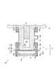
図2は、一実施形態によるイメージセンサ装置10の外観を示す斜視図である。図3は、イメージセンサ装置10の正面図である。図4は、図2のIV−IV線に沿ったイメージセンサ装置10の部分断面図である。図2〜図4に示されるように、本実施形態のイメージセンサ装置10は、本体部11及び小型冷却機12を備える。本体部11は、光入射窓13(図2では図示を省略)、気密封止筐体14、ヘッド15、マウント16、イメージセンサ素子17、枠部18、及びフィードスルー20Aを有する。光入射窓13、気密封止筐体14、枠部18、及びフィードスルー20Aは、イメージセンサ素子17を収容する容器11aを構成する。 FIG. 2 is a perspective view illustrating an appearance of the
光入射窓13は、入射光像Laを透過する板状の部材である。光入射窓13は、後述するイメージセンサ素子17と対向して配置されている。光入射窓13の構成材料は、入射光像Laの波長に応じて決定される。例えば、入射光像Laの波長が1.2μm〜6μmである場合、光入射窓13の構成材料としてはシリコンが選択される。入射光像Laの入射方向から見た光入射窓13の形状は円形である。光入射窓13の周縁部には、光入射窓13を保持するための円環状の枠部18が取り付けられている。枠部18は、例えば金属製である。枠部18と光入射窓13とは、気密を維持するように互いに密着している。 The
気密封止筐体14は、或る方向A1に沿って延びる略円筒状の外観を有する。気密封止筐体14の構成材料は、例えばステンレスといった金属である。気密封止筐体14の外周面は、本体部11の外周面を構成する。方向A1における気密封止筐体14の一端には、光入射窓13を保持する枠部18が気密に固定されている。これにより、方向A1における気密封止筐体14の開口が、光入射窓13によって閉じられる。方向A1は、光入射窓13の厚さ方向と一致する。すなわち、方向A1は、入射光像Laの入射方向と一致する。 The hermetically sealed
より具体的には、気密封止筐体14は、円環状の第1部材14a、円環状の第2部材14b、及び略円筒状の第3部材14cを含んで構成されている。第1部材14a及び第2部材14bは、方向A1において第3部材14cと枠部18との間に並んで配置されている。第1部材14a、第2部材14b及び第3部材14cは、方向A1から見て互いに重なっている。すなわち、第1部材14a、第2部材14b及び第3部材14cの各内部空間は、方向A1に沿って連通している。枠部18は、例えばボルトといった締結部材19aによって第1部材14aの一端面に固定されている。枠部18と第1部材14aとの隙間は、気密に封止されている。第3部材14cの一端面は、例えばボルトといった締結部材19bによって第2部材14bの一端面に固定されている。第2部材14bと第3部材14cとの隙間は、気密に封止されている。第3部材14cの他端面は、例えばボルトといった締結部材19cによって小型冷却機12に固定されている。第3部材14cと小型冷却機12との隙間は、気密に封止されている。第1部材14aの他端面と第2部材14bの他端面との間には、フィードスルー20Aが挟持されている。言い換えれば、第1部材14aと第2部材14bとは、フィードスルー20Aを介して互いに接合され、一体化されている。 More specifically, the hermetic sealing
第3部材14cの外側面からは、真空引き用の一つのチューブ14dが突出している。チューブ14dは気密封止筐体の内部空間に通じている。チューブ14dを介して気密封止筐体14の内部が真空引きされたのち(若しくは不活性ガスが充填されたのち)、チューブ14dの先端は気密に封じられる。 One
ヘッド15は、気密封止筐体14の内部に設けられた、方向A1に沿って延びる略円筒状の金属製の部材である。ヘッド15の外周面は、気密封止筐体14の内周面と空隙を介して対向している。この空隙は、真空状態に維持されるか、不活性ガスが充填されている。方向A1におけるヘッド15の一端は閉じられており、他端は小型冷却機12に固定されている。他端側の開口には、小型冷却機12のピストン31が挿入される。ヘッド15の内部には空間32が設けられており、方向A1に沿ったピストン31の往復動作によって、空間32の容積が増加と減少とを繰り返す。空間32にはヘリウムガスが封入されており、空間32の容積の変化に伴い、ヘッド15の温度が低下する。方向A1におけるヘッド15の一端は方向A1と交差する平坦面となっており、該平坦面上にマウント16が設けられる。 The
マウント16は、イメージセンサ素子17を搭載する板状の部材である。マウント16は、方向A1から見て四角形状を呈している。マウント16の一方の板面はヘッド15の平坦面に接合されており、他方の板面はイメージセンサ素子17を収容するための凹部を成している。マウント16の構成材料は、例えば窒化アルミニウムといったセラミックスである。マウント16は、イメージセンサ素子17をヘッド15に固定するとともに、イメージセンサ素子17とヘッド15とを熱的に結合する。 The
イメージセンサ素子17は、入射光像Laを電気的な画像信号Saに変換する半導体素子である。イメージセンサ素子17は、例えばインジウムガリウム砒素(InGaAs)といった半導体材料によって主に構成され、波長が0.9μm〜1.7μmに感度を有する赤外センサアレイである。イメージセンサ素子17は、光入射窓13、気密封止筐体14、ヘッド15、枠部18、及びフィードスルー20Aによって構成される容器11a内に気密に収容されている。方向A1から見たイメージセンサ素子17の平面形状は例えば四角形であり、マウント16の平面形状の相似形である。 The
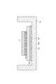
図5は、マウント16及びイメージセンサ素子17の周辺構造を概略的に示す断面図である。図5に示されるように、マウント16は、ヘッド15と対向する裏面16aと、裏面16aの反対側に設けられた搭載面16bとを有する。搭載面16bは、凹部の底面を構成している。搭載面16b上には制御IC33が実装されており、更にその上にイメージセンサ素子17が実装されている。制御IC33は、例えば銀ペーストといった導電性接着剤34を介して搭載面16bに固定されている。イメージセンサ素子17は、光入射面とは反対側の裏面に設けられた複数のバンプ電極35を介して、制御IC33と電気的に接続されている。制御基板4との間で信号を授受するための制御IC33の複数の端子は、マウント16上に設けられた複数の端子にそれぞれボンディングワイヤで接続され、更にその端子からフィードスルーへもボンディングワイヤで接続されている。マウント16上の複数の端子は、マウント16の凹部内からマウント16の縁へ延びている。 FIG. 5 is a cross-sectional view schematically showing the peripheral structure of the
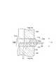
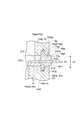
ここで、フィードスルー20Aの詳細な構造について説明する。図6(a)は、フィードスルー20A及びその周辺構造を拡大して示す斜視図である。同図において光入射窓13及び枠部18の図示は省略されている。図6(b)は、図6(a)のB部の拡大図である。また、図7は、フィードスルー20Aの外側面付近の構成を拡大して示す、方向A1に沿った断面図である。 Here, the detailed structure of the
フィードスルー20Aは、容器11aの内部に設けられた制御IC33と、容器11aの外部に設けられた制御基板4とを電気的に導通させるための構造体である。フィードスルー20Aは、絶縁部材21と、複数の導体22と、変形緩和材23Aとを有する。絶縁部材21は、気密封止筐体14の第1部材14a及び第2部材14bと共通の中心軸線を有する円環状の部材であって、イメージセンサ素子17を収容する容器11aの一部を構成する。絶縁部材21は、容器11aの内側を向く内側面21aと、容器11aの外側を向く外側面21b(図7を参照)とを有し、容器11aの内部と外部とを仕切る。絶縁部材21の材料としては、電気絶縁性及び気密性の観点から、例えばガラス或いはセラミックといった絶縁材料が用いられる。これらの材料は、フィードスルー20Aに求められる耐圧性能や耐熱性能に応じて選択される。本実施形態の絶縁部材21は、ガラス及びセラミックの少なくとも一方を主に含む。 The
複数の導体22は、例えばステンレスといった金属(若しくは、高い硬度が必要な場合には合金)に例えば金メッキされた導電性の部材である。複数の導体22は、板状であり、絶縁部材21の内側面21aと外側面21bとの間を貫通している。また、複数の導体22は、絶縁部材21の周方向(本実施形態における所定方向)に一列に並んでいる。該周方向において、複数の導体22の間隔は均一である。また、該周方向において、複数の導体22は全周にわたって配置されている。複数の導体22の両端のうち、容器11aの内部に位置する一端は、ボンディングワイヤを介してマウント16上の複数の端子とそれぞれ電気的に接続されている。容器11aの外部に位置する他端は、例えば半田等の導電性接着剤を介して制御基板4に導電接合される。なお、制御基板4は、円形の開口を有しており、本体部11が該開口に挿入される形で複数の導体22と接している。 The plurality of
導体22は、外側面21bと交差する方向を長手方向とする板状を呈しており、互いに対向する一対の板面を有している。一対の板面は互いに平行である。導体22の一対の板面は、絶縁部材21の周方向(複数の導体22の並び方向)に沿っている。そして、複数の導体22のうち容器11aの内側に位置する部分は、絶縁部材21の周方向に沿って並んで配置されている。容器11aの内側において、導体22の板面は或る仮想平面に沿って面一に並んでいる。複数の導体22のうち容器11aの外側に位置する部分もまた、絶縁部材21の周方向に沿って並んで配置されている。容器11aの外側において、導体22の板面は該仮想平面に沿って面一に並んでいる。 The
図7に示されるように、絶縁部材21の外側面21bは、第1部材14aの外側面14e、及び第2部材14bの外側面14fに対して、内側面21a側に位置している。従って、絶縁部材21の外側面21bは、第1部材14aの端面14g、第2部材14bの端面14h、及び外側面21bによって容器11aの外側面に形成される凹部の底面を構成している。端面14g及び14hは方向A1において互いに対向している。本実施形態では、端面14g及び14hは方向A1に垂直な平面に沿っており、外側面21bに対して垂直であり且つ互いに平行である。 As shown in FIG. 7, the
変形緩和材23Aは、絶縁部材21の外側面21b上に設けられている。変形緩和材23Aは、絶縁部材21の外側に位置する(絶縁部材21から露出した)各導体22の一部を覆う。但し、各導体22の外側の端部は変形緩和材23Aから露出している。変形緩和材23Aは、第1部材14aの端面14g、第2部材14bの端面14h、及び絶縁部材21の外側面21bによって形成される凹部を埋め込んでおり、端面14g、端面14h、及び外側面21bに固着している。 The deformation moderating material 23 </ b> A is provided on the
変形緩和材23Aは、絶縁部材21よりも変形し易い(すなわち、絶縁部材21よりもヤング率が小さい)材料からなる。変形緩和材23Aは、例えば樹脂を主に含む。樹脂は、例えば硬度が比較的高いエポキシ樹脂であってもよく、若しくは、硬度が比較的低いシリコン樹脂であってもよい。また、変形緩和材23Aは絶縁性である。変形緩和材23Aの絶縁部材21とは反対側の外側面23aは、方向A1に沿っている。すなわち、導体22の並び方向と垂直な断面において、外側面23aは方向A1に沿って真っ直ぐに延びている。導体22は、外側面23aから、外側面23aに対して垂直な方向に突出している。 The deformation moderating material 23 </ b> A is made of a material that is easier to deform than the insulating member 21 (that is, Young's modulus is smaller than that of the insulating member 21). The
以上に説明した本実施形態の撮像装置1A及びイメージセンサ装置10によって得られる効果について、従来の課題とともに説明する。図15(a)は、比較例に係るイメージセンサ装置のフィードスルー120及びその周辺構造を拡大して示す斜視図である。同図において光入射窓13及び枠部18の図示は省略されている。図15(b)は、図15(a)のC部の拡大図である。図15に示されるように、フィードスルー120では、板状の複数の導体22が所定方向に並んで配置され、且つ各導体22の板面が或る仮想平面に沿って面一に並んでいる。これにより、制御基板4と複数の導体22との導電接着が容易となる。 The effects obtained by the
しかしながら、制御基板4と複数の導体22とを導電性接着剤によって固着する際、導体22に力が加わり、絶縁部材21の導体貫通用の孔付近に応力が発生する。或いは、複数の導体22と制御基板4とが固着された後の制御基板4への外力によっても、導体22を介して絶縁部材21に同様の応力が発生する。このような応力によって絶縁部材21に亀裂CLが生じ、容器の気密状態を維持できなくなる虞がある。本発明者の知見によれば、フィードスルー120の絶縁部材21に生じる亀裂CLは、板状導体22と絶縁部材21との界面を起点として、該界面に生じる応力に垂直な面に沿って伸展する傾向がある。従って、複数の板状導体22の板面が一つの仮想平面に沿って面一に並ぶフィードスルー120では、互いに隣り合う板状導体22間で応力に垂直な面同士が重なり、亀裂CLが生じやすくなる。 However, when the
このような課題に対し、本実施形態のイメージセンサ装置10では、絶縁部材21の外側に位置する各導体22の一部が、絶縁部材21よりも変形し易い変形緩和材23Aによって覆われている。そして、変形緩和材23Aは、絶縁部材21に固着している。従って、導体22に力が加わった場合に、応力を変形緩和材23Aが受け、該応力を絶縁部材21に分散して伝える。従って、本実施形態の撮像装置1A及びイメージセンサ装置10によれば、絶縁部材21に生じる局所的な応力を抑制し、絶縁部材21の亀裂を低減できる。 With respect to such a problem, in the
また、本実施形態のように、絶縁部材21はガラス及びセラミックの少なくとも一方を含み、変形緩和材23Aは樹脂を含んでもよい。例えばこれらのような構成材料によって、変形緩和材23Aを絶縁部材21よりも変形し易くすることができる。 Further, as in the present embodiment, the insulating
また、本実施形態のように、変形緩和材23Aは絶縁性であってもよい。これにより、隣り合う導体22間の絶縁状態を容易に維持することができる。 Further, as in the present embodiment, the
また、本実施形態のように、絶縁部材21は、容器11aの外側面に形成された凹部の底面を構成し、変形緩和材23Aは凹部を埋め込んでもよい。これにより、絶縁部材21と変形緩和材23Aとの固着強度が増し、導体22の曲げによる絶縁部材21からの変形緩和材23Aの剥離を低減できるので、イメージセンサ装置10の信頼性を向上できる。また、変形緩和材23Aの移動を絶縁部材21の凹部によって抑えることができるので、導体22に力が加わった際の導体22の曲げを抑制できる。 In addition, as in the present embodiment, the insulating
また、本実施形態のように、複数の導体22の断面形状は長方形であってもよい。このような場合、長方形の角部に位置する絶縁部材21に応力が集中しやすく亀裂CLが生じ易いので、本実施形態のイメージセンサ装置10の構成が特に有効である。 Further, as in the present embodiment, the cross-sectional shape of the plurality of
(第1変形例)
図8は、上記実施形態の第1変形例に係るイメージセンサ装置のフィードスルー20Bの外側面付近の構成を拡大して示す断面図である。本変形例のフィードスルー20Bは、上記実施形態の変形緩和材23Aに代えて、変形緩和材23Bを有する。変形緩和材23Bの構成材料は、上記実施形態と同様である。(First modification)
FIG. 8 is an enlarged cross-sectional view showing the configuration near the outer surface of the
変形緩和材23Bは、絶縁部材21と接する面とは反対側に位置する外側面23bを有する。外側面23bは、第1部材14aの外側面14e及び第2部材14bの外側面14fによって規定される円柱面に対して外側(絶縁部材21とは反対側)へ突出している。これにより、本変形例の変形緩和材23Bは、上記実施形態の変形緩和材23Aと比較して、導体22のより長い部分を覆っている。従って、本変形例によれば、上記実施形態と比較して、絶縁部材21に生じる局所的な応力を更に抑制し、絶縁部材21の亀裂をより効果的に低減できる。 The deformation moderating material 23 </ b> B has an
(第2変形例)
図9は、上記実施形態の第2変形例に係るイメージセンサ装置のフィードスルー20Cの外側面付近の構成を拡大して示す断面図である。本変形例のフィードスルー20Cは、上記実施形態の変形緩和材23Aに代えて、変形緩和材23Cを有する。変形緩和材23Cの構成材料は、上記実施形態と同様である。また、変形緩和材23Cの外側面23bの形状は、第1変形例と同様である。(Second modification)
FIG. 9 is an enlarged cross-sectional view showing the configuration near the outer surface of the
本変形例では、第1部材14aの端面14g、及び第2部材14bの端面14hに段差14i,14jがそれぞれ形成されている。これにより、段差14i,14jに対して内側に位置する端面14ga,14haの方向A1における間隔W1よりも、段差14i,14jに対して外側に位置する端面14gb,14hbの方向A1における間隔W2のほうが広くなっている。端面14ga及び端面14haには絶縁部材21が接し、端面14gb及び端面14hbには変形緩和材23Cが接する。従って、方向A1における変形緩和材23Cの厚さは、同方向における絶縁部材21の厚さよりも厚くなっている。変形緩和材は、本変形例のような形状を有してもよく、第1変形例と同様の効果を奏することができる。 In this modification,
(第3変形例)
図10は、上記実施形態の第3変形例に係るイメージセンサ装置のフィードスルー20Dの外側面付近の構成を拡大して示す断面図である。本変形例のフィードスルー20Dは、上記実施形態の変形緩和材23Aに代えて、変形緩和材23Dを有する。変形緩和材23Dの構成材料は、上記実施形態と同様である。また、変形緩和材23Dの外側面23bの形状は、第1変形例と同様である。(Third Modification)
FIG. 10 is an enlarged cross-sectional view showing the configuration near the outer surface of the
本変形例では、第1部材14aの端面14gが、端面14gaと、端面14gaに対して外側に位置する端面14gcとを含んでいる。同様に、第2部材14bの端面14hが、端面14haと、端面14haに対して外側に位置する端面14hcとを含んでいる。端面14ga及び端面14haには絶縁部材21が接し、端面14gc及び端面14hcには変形緩和材23Dが接する。端面14ga及び14haは、方向A1に対して垂直な平面に沿っている。これに対し、端面14gc及び14hcは、互いの間隔が外側に向けて徐々に拡がるように、該平面に対して傾斜している。言い換えれば、端面14gと外側面14eとにより構成される角は面取りされており、端面14hと外側面14fとにより構成される角もまた面取りされている。従って、方向A1における変形緩和材23Dの厚さは、外側に向けて徐々に拡大している。変形緩和材23Dの絶縁部材21と接する部分の厚さは、絶縁部材21の厚さと等しく、変形緩和材23Dの外側面14e,14fと接する部分の厚さよりも薄い。 In the present modification, the
変形緩和材は、本変形例のような形状を有してもよく、第1変形例と同様の効果を奏することができる。また、変形緩和材23Dと接する端面14g,14hの間隔が外側に向けて徐々に拡がることにより、凹部内に変形緩和材23Dの材料を配置し易くなるので、変形緩和材23Dの形成を容易にできる。 The deformation moderating material may have a shape as in the present modification example, and can exhibit the same effects as in the first modification example. Moreover, since the space | interval of the end surfaces 14g and 14h which contact | connect the deformation |
(第4変形例)
図11は、上記実施形態の第4変形例に係るイメージセンサ装置のフィードスルー20Eの外側面付近の構成を拡大して示す断面図である。本変形例のフィードスルー20Eは、上記実施形態の変形緩和材23Aに代えて、変形緩和材23Eを有する。変形緩和材23Eの構成材料は、上記実施形態と同様である。本変形例では、絶縁部材21の外側面21bは凹部を形成しておらず、第1部材14aの外側面14e及び第2部材14bの外側面14fと面一になっている。そして、変形緩和材23Eは、外側面21b、外側面14e、及び外側面14fによって構成される円柱面上において、主に外側面21b上に設けられている。変形緩和材23Eの方向A1における一端は外側面14eに接してもよく、他端は外側面14fに接してもよい。また、変形緩和材23Eは、絶縁部材21と接する面とは反対側に位置する外側面23eを有する。導体22の並び方向に垂直な断面における外側面23eの形状は、例えば半円状である。変形緩和材は、本変形例のような形状を有してもよい。このような場合であっても、上記実施形態と同様の効果を奏することができる。(Fourth modification)
FIG. 11 is an enlarged cross-sectional view showing the configuration near the outer surface of the
(第5変形例)
図12は、上記実施形態の第5変形例に係るイメージセンサ装置のフィードスルー20Fの外側面付近の構成を拡大して示す断面図である。本変形例のフィードスルー20Fは、上記実施形態の変形緩和材23Aに代えて、変形緩和材23Fを有する。変形緩和材23Fの構成材料は、上記実施形態と同様である。また、変形緩和材23Fの外側面23bの形状は、第1変形例と同様である。(5th modification)
FIG. 12 is an enlarged cross-sectional view showing the configuration near the outer surface of the
第1部材14aの端面14gは、端面14gaと、端面14gaに対して外側に位置する凹部14gdとを含んでいる。同様に、第2部材14bの端面14hは、端面14haと、端面14haに対して外側に位置する凹部14hdとを含んでいる。端面14ga,14haには絶縁部材21が接し、凹部14gd,14hdには変形緩和材23Fが接する。端面14ga及び14haは、方向A1に対して垂直な平面に沿っている。凹部14gd,14hdの一対の内側面のうち内側に位置する内側面14gf,14hfは、方向A1に沿っている。凹部14gd,14hdの一対の内側面のうち外側に位置する内側面14ge,14heは、互いの間隔が外側に向けて徐々に狭くなるように、該平面に対して傾斜している。従って、方向A1における変形緩和材23Fの厚さは、絶縁部材21と接する部分の近傍においては絶縁部材21の厚さよりも厚くなり、外側に向けて徐々に薄くなる。 The
図13は、本変形例の別の例に係るフィードスルー20Gの外側面付近の構成を拡大して示す断面図である。本変形例のフィードスルー20Gは、上記実施形態の変形緩和材23Aに代えて、変形緩和材23Gを有する。変形緩和材23Gの構成材料は、上記実施形態と同様である。また、変形緩和材23Gの外側面23bの形状は、第1変形例と同様である。 FIG. 13 is an enlarged cross-sectional view showing a configuration near the outer surface of a
この例においても、第1部材14aの端面14gは、端面14gaと、端面14gaに対して外側に位置する凹部14gdとを含んでおり、第2部材14bの端面14hは、端面14haと、端面14haに対して外側に位置する凹部14hdとを含んでいる。端面14ga,14haには絶縁部材21が接し、凹部14gd,14hdには変形緩和材23Gが接する。但し、この例では凹部14gd,14hdの形状が上記の例とは異なっており、凹部14gd,14hdの一対の内側面のうち外側に位置する内側面14gg,14hgは、方向A1に沿っており、内側に位置する内側面14gf,14hfと対向している。また、凹部14gd,14hdの更に外側には、方向A1に対して垂直な平面に沿った端面14gh及び14hhが設けられている。端面14gh及び14hhの間隔は、端面14ga及び14haの間隔と等しい。従って、変形緩和材23Gは、絶縁部材21と接する部分を含む肉厚部23Gaと、その外側に位置する肉薄部23Gbとを含む。方向A1における肉厚部23Gaの厚さは、同方向における肉薄部23Gbの厚さよりも厚い。 Also in this example, the
変形緩和材は、図12,図13に示されたような形状を有してもよく、第1変形例と同様の効果を奏することができる。また、絶縁部材21と接する部分の周辺における変形緩和材23F,23Gの体積が上記実施形態及び第1変形例よりも大きくなるので、導体22に力が加わった場合に、応力をより効果的に分散して絶縁部材21に伝えることができる。従って、絶縁部材21の亀裂を更に低減できる。 The deformation moderating material may have a shape as shown in FIGS. 12 and 13 and can provide the same effects as those of the first modification. Moreover, since the volume of the
(第6変形例)
図14(a)は、上記実施形態の第6変形例に係るイメージセンサ装置のフィードスルー20H及びその周辺構造を拡大して示す斜視図である。同図において光入射窓13及び枠部18の図示は省略されている。図14(b)は、フィードスルー20Hを部分的に拡大して示す側面図である。(Sixth Modification)
FIG. 14A is an enlarged perspective view showing the
本変形例のフィードスルー20Hは、上記実施形態のフィードスルー20Aが有する絶縁部材21に代えて、絶縁部材27を有する。絶縁部材27は、上記実施形態の絶縁部材21とは異なり、方向A1(光入射方向)から見て四角形状(正方形状、長方形状、或いは台形状)を呈している。絶縁部材21は、マウント16及びイメージセンサ素子17を収容する容器の内側を向く内側面27aと、該容器の外側を向く外側面27bとを有し、該容器の内部と外部とを仕切る。絶縁部材27は、上記実施形態の絶縁部材21と同様に、例えばガラス、セラミック、或いは樹脂といった絶縁体からなる。 The
内側面27a及び外側面27bは、方向A1と直交する方向A3に沿って真っ直ぐに延びている。すなわち、上記実施形態では複数の導体22の並び方向が円周面に沿っていたが、本変形例では、複数の導体22の並び方向A3が平面に沿っている。方向A3において、複数の導体22の間隔は均一である。 The
更に、本変形例では、外側面27b上に変形緩和材23Hが設けられている。並び方向A3に垂直な平面に沿った断面における変形緩和材23Hの形状は、上記実施形態と同様である。また、変形緩和材23Hの構成材料は、上記実施形態と同様である。本変形例のような構成においても、上記実施形態と同様の効果を奏することができる。 Further, in the present modification, a
本発明によるイメージセンサ装置及び撮像装置は、上述した実施形態及び各変形例に限られるものではなく、他に様々な変形が可能である。例えば、上述した実施形態及び各変形例を、必要な目的及び効果に応じて互いに組み合わせてもよい。また、変形緩和材の形状は上記実施形態及び各変形例に限られず、他の様々な形状が可能である。例えば、上記実施形態及び各変形例では、複数の導体の並び方向に延びる単一の変形緩和材によって複数の導体を覆っているが、複数の変形緩和材が各導体毎に間隔をあけて設けられてもよい。また、上記実施形態及び各変形例では、絶縁部材と気密封止筐体とによって凹部が形成されているが、絶縁部材の外側面が導体の長手方向に窪むことによって凹部が形成されてもよい。その場合、絶縁部材に形成された凹部の内面が、図12、図13に示された凹部14gd,14hdのような形状を有してもよい。 The image sensor device and the imaging device according to the present invention are not limited to the above-described embodiments and modifications, and various other modifications are possible. For example, the above-described embodiments and modifications may be combined with each other according to the necessary purpose and effect. In addition, the shape of the deformation moderating material is not limited to the above-described embodiment and each modification, and various other shapes are possible. For example, in the above-described embodiment and each modification, the plurality of conductors are covered with a single deformation moderating material extending in the arrangement direction of the plurality of conductors, but the plurality of deformation moderation materials are provided at intervals for each conductor. May be. Moreover, in the said embodiment and each modification, although the recessed part is formed with the insulating member and the airtight sealing housing | casing, even if a recessed part is formed because the outer surface of an insulating member sinks in the longitudinal direction of a conductor. Good. In that case, the inner surface of the recess formed in the insulating member may have a shape like the recesses 14gd and 14hd shown in FIGS.
1A…撮像装置、3…レンズ、4…制御基板、5…コントローラ、6…信号処理部、7…信号記憶部、8…画像表示部、10…イメージセンサ装置、11…本体部、11a…容器、12…小型冷却機、13…光入射窓、14…気密封止筐体、14a…第1部材、14b…第2部材、14c…第3部材、14d…チューブ、15…ヘッド、16…マウント、16a…裏面、16b…搭載面、17…イメージセンサ素子、18…枠部、19a,19b,19c…締結部材、20A〜20H…フィードスルー、21,27…絶縁部材、21a,27a…内側面、21b,27b…外側面、22…導体、23A〜23H…変形緩和材、31…ピストン、32…空間、33…制御IC、34…導電性接着剤、35…バンプ電極、CL…亀裂、Da…画像データ、La…入射光像、Sa…画像信号、Sc…制御信号。 DESCRIPTION OF
Claims (6)
Translated fromJapanese前記イメージセンサ素子を気密に収容する容器と、を備え、
前記容器は、
前記イメージセンサ素子と対向して配置され前記入射光像を透過する光入射窓と、
前記容器の一部を構成する絶縁部材、及び前記絶縁部材を貫通し所定方向に並ぶ板状の複数の導体を含み、前記容器の内部と外部とを電気的に導通させるフィードスルーと、
を有し、
前記フィードスルーは、前記絶縁部材の外側に位置する各導体の一部を覆うとともに前記絶縁部材に固着し、前記絶縁部材よりも変形し易い変形緩和材を更に含む、イメージセンサ装置。An image sensor element for converting an incident light image into an electrical image signal;
A container for airtightly storing the image sensor element,
The container is
A light incident window disposed opposite to the image sensor element and transmitting the incident light image;
An insulating member constituting a part of the container, and a plurality of plate-like conductors that penetrate the insulating member and are arranged in a predetermined direction, and a feedthrough that electrically connects the inside and the outside of the container;
Have
The image sensor device further includes a deformation mitigating material that covers a part of each conductor located outside the insulating member, is fixed to the insulating member, and is easier to deform than the insulating member.
前記変形緩和材は樹脂を含む、請求項1に記載のイメージセンサ装置。The insulating member includes at least one of glass and ceramic,
The image sensor device according to claim 1, wherein the deformation moderating material includes a resin.
前記変形緩和材の少なくとも一部は前記凹部を埋め込んでいる、請求項1〜3のいずれか一項に記載のイメージセンサ装置。The insulating member constitutes a bottom surface of a recess formed on the outer surface of the container;
The image sensor device according to claim 1, wherein at least a part of the deformation relaxation material embeds the recess.
前記容器の外部に位置する前記複数の導体の端部と電気的に接続された基板と、
前記基板から得られる信号を画像信号に変換する信号処理部と、
を備える、撮像装置。The image sensor device according to any one of claims 1 to 5,
A substrate electrically connected to ends of the plurality of conductors located outside the container;
A signal processing unit for converting a signal obtained from the substrate into an image signal;
An imaging apparatus comprising:
Priority Applications (2)
| Application Number | Priority Date | Filing Date | Title |
|---|---|---|---|
| JP2017160143AJP2019041172A (en) | 2017-08-23 | 2017-08-23 | Image sensor device and imaging device |
| US16/107,313US20190068847A1 (en) | 2017-08-23 | 2018-08-21 | Optical sensor and imaging apparatus |
Applications Claiming Priority (1)
| Application Number | Priority Date | Filing Date | Title |
|---|---|---|---|
| JP2017160143AJP2019041172A (en) | 2017-08-23 | 2017-08-23 | Image sensor device and imaging device |
Publications (1)
| Publication Number | Publication Date |
|---|---|
| JP2019041172Atrue JP2019041172A (en) | 2019-03-14 |
Family
ID=65438023
Family Applications (1)
| Application Number | Title | Priority Date | Filing Date |
|---|---|---|---|
| JP2017160143APendingJP2019041172A (en) | 2017-08-23 | 2017-08-23 | Image sensor device and imaging device |
Country Status (2)
| Country | Link |
|---|---|
| US (1) | US20190068847A1 (en) |
| JP (1) | JP2019041172A (en) |
Families Citing this family (8)
| Publication number | Priority date | Publication date | Assignee | Title |
|---|---|---|---|---|
| US11077825B2 (en) | 2019-12-16 | 2021-08-03 | Plusai Limited | System and method for anti-tampering mechanism |
| US11313704B2 (en)* | 2019-12-16 | 2022-04-26 | Plusai, Inc. | System and method for a sensor protection assembly |
| US11650415B2 (en) | 2019-12-16 | 2023-05-16 | Plusai, Inc. | System and method for a sensor protection mechanism |
| US11754689B2 (en) | 2019-12-16 | 2023-09-12 | Plusai, Inc. | System and method for detecting sensor adjustment need |
| US11738694B2 (en) | 2019-12-16 | 2023-08-29 | Plusai, Inc. | System and method for anti-tampering sensor assembly |
| US11724669B2 (en) | 2019-12-16 | 2023-08-15 | Plusai, Inc. | System and method for a sensor protection system |
| US11470265B2 (en) | 2019-12-16 | 2022-10-11 | Plusai, Inc. | System and method for sensor system against glare and control thereof |
| US11772667B1 (en) | 2022-06-08 | 2023-10-03 | Plusai, Inc. | Operating a vehicle in response to detecting a faulty sensor using calibration parameters of the sensor |
Citations (5)
| Publication number | Priority date | Publication date | Assignee | Title |
|---|---|---|---|---|
| JPH02105495A (en)* | 1988-10-13 | 1990-04-18 | Nec Corp | Hybrid integrated circuit device |
| JPH1084509A (en)* | 1996-09-06 | 1998-03-31 | Matsushita Electron Corp | Imaging device and method of manufacturing the same |
| JP2002231375A (en)* | 2001-01-30 | 2002-08-16 | Yazaki Corp | Auxiliary module sealing structure |
| JP2005347336A (en)* | 2004-05-31 | 2005-12-15 | Matsushita Electric Works Ltd | Solid-state imaging device storage package |
| JP2012049377A (en)* | 2010-08-27 | 2012-03-08 | Kyocera Corp | Package for housing imaging element and imaging device |
Family Cites Families (2)
| Publication number | Priority date | Publication date | Assignee | Title |
|---|---|---|---|---|
| US6483101B1 (en)* | 1999-12-08 | 2002-11-19 | Amkor Technology, Inc. | Molded image sensor package having lens holder |
| US20070258006A1 (en)* | 2005-08-25 | 2007-11-08 | Olsen Richard I | Solid state camera optics frame and assembly |
- 2017
- 2017-08-23JPJP2017160143Apatent/JP2019041172A/enactivePending
- 2018
- 2018-08-21USUS16/107,313patent/US20190068847A1/ennot_activeAbandoned
Patent Citations (5)
| Publication number | Priority date | Publication date | Assignee | Title |
|---|---|---|---|---|
| JPH02105495A (en)* | 1988-10-13 | 1990-04-18 | Nec Corp | Hybrid integrated circuit device |
| JPH1084509A (en)* | 1996-09-06 | 1998-03-31 | Matsushita Electron Corp | Imaging device and method of manufacturing the same |
| JP2002231375A (en)* | 2001-01-30 | 2002-08-16 | Yazaki Corp | Auxiliary module sealing structure |
| JP2005347336A (en)* | 2004-05-31 | 2005-12-15 | Matsushita Electric Works Ltd | Solid-state imaging device storage package |
| JP2012049377A (en)* | 2010-08-27 | 2012-03-08 | Kyocera Corp | Package for housing imaging element and imaging device |
Also Published As
| Publication number | Publication date |
|---|---|
| US20190068847A1 (en) | 2019-02-28 |
Similar Documents
| Publication | Publication Date | Title |
|---|---|---|
| JP2019041172A (en) | Image sensor device and imaging device | |
| US8624339B2 (en) | Vibrating device and electronic apparatus | |
| JP5645245B2 (en) | Infrared sensor module | |
| US20070241451A1 (en) | Electronic component device | |
| EP3432353A1 (en) | High frequency circuit | |
| US9664581B2 (en) | Pressure sensor, electronic apparatus, and moving object | |
| WO2013015216A1 (en) | Package for accommodating semiconductor element, semiconductor device provided with same, and electronic device | |
| US9420691B2 (en) | Electronic device, method for manufacturing thereof, and electronic apparatus | |
| US11650054B2 (en) | Vibrator device, electronic apparatus, and vehicle | |
| TWI473214B (en) | Packaging devices and packaging substrates | |
| US20180269850A1 (en) | Vibrator device, oscillator, electronic device, and vehicle | |
| JP2014082348A (en) | Package for storing optical element, optical filter device, optical module, and electronic apparatus | |
| CN112311348B (en) | Vibration device, electronic apparatus, and moving object | |
| CN216899259U (en) | Infrared detector module and infrared thermal imaging device | |
| JP2014239215A (en) | Semiconductor detector head and manufacturing method therefor | |
| WO2024222609A1 (en) | Electronic assembly and electronic device | |
| JP6870534B2 (en) | Image sensor device and imaging device | |
| CN113341513A (en) | Optical module | |
| JP2013062339A (en) | Composite substrate, electronic device, and electronic apparatus | |
| US12051707B2 (en) | Imaging element unit and imaging device | |
| US20140345928A1 (en) | Electronic part, electronic apparatus, and moving object | |
| JP2013093494A (en) | Package for housing electronic component and electronic device | |
| CN107063225A (en) | Electronic installation, the manufacture method of electronic installation, electronic equipment and moving body | |
| JP5844005B2 (en) | High frequency circuit equipment | |
| CN100445820C (en) | Electronic device and its packaging structure |
Legal Events
| Date | Code | Title | Description |
|---|---|---|---|
| A621 | Written request for application examination | Free format text:JAPANESE INTERMEDIATE CODE: A621 Effective date:20200323 | |
| A977 | Report on retrieval | Free format text:JAPANESE INTERMEDIATE CODE: A971007 Effective date:20201113 | |
| A131 | Notification of reasons for refusal | Free format text:JAPANESE INTERMEDIATE CODE: A131 Effective date:20201208 | |
| A02 | Decision of refusal | Free format text:JAPANESE INTERMEDIATE CODE: A02 Effective date:20210629 |