JP2019039756A - probe - Google Patents
probeDownload PDFInfo
- Publication number
- JP2019039756A JP2019039756AJP2017161169AJP2017161169AJP2019039756AJP 2019039756 AJP2019039756 AJP 2019039756AJP 2017161169 AJP2017161169 AJP 2017161169AJP 2017161169 AJP2017161169 AJP 2017161169AJP 2019039756 AJP2019039756 AJP 2019039756A
- Authority
- JP
- Japan
- Prior art keywords
- barrel
- base
- probe
- probe according
- spring portion
- Prior art date
- Legal status (The legal status is an assumption and is not a legal conclusion. Google has not performed a legal analysis and makes no representation as to the accuracy of the status listed.)
- Granted
Links
Images


Landscapes
- Measuring Leads Or Probes (AREA)
- Testing Or Measuring Of Semiconductors Or The Like (AREA)
Abstract
Translated fromJapaneseDescription
Translated fromJapanese本発明は、被検査体の特性の測定に使用されるプローブに関する。 The present invention relates to a probe used for measuring characteristics of an object to be inspected.
集積回路などの特性をウェハから分離しない状態で測定するために、プローブが用いられている。プローブを用いた検査では、プローブの一方の端部を被検査体に接触させ、プローブの他方の端部を、基板に配置されてテスタと電気的に接続された端子(以下において「ランド」という。)に接触させる。 Probes are used to measure characteristics such as integrated circuits without being separated from the wafer. In the inspection using the probe, one end of the probe is brought into contact with the object to be inspected, and the other end of the probe is a terminal (hereinafter referred to as “land”) that is disposed on the substrate and electrically connected to the tester. .)
検査において、被検査体やランドとプローブとの電気的な接続を確保する必要がある。このため、プローブを強く被検査体に押し付けるためにオーバードライブ(OD)をかけたり、プローブを弾性変形させることによってプローブとランドにプリロードをかけたりしている。このため、弾性変形する部分をプローブに設ける構造が採用されている(例えば特許文献1参照。)。 In the inspection, it is necessary to ensure electrical connection between the inspection object or land and the probe. For this reason, overdrive (OD) is applied to strongly press the probe against the object to be inspected, or the probe and the land are preloaded by elastically deforming the probe. For this reason, the structure which provides the part which elastically deforms in a probe is employ | adopted (for example, refer patent document 1).
プリロードとODの両方を1本のプローブの弾性変形によってかけるために、プローブの全長を長くすることが必要である。例えば、全長が8mm程度のプローブが使用されている。このような全長の長いプローブは、使用によって撓みが生じやすい。その結果、隣接するプローブ間での接触(以下において「隣接ショート」という。)が発生するという問題が生じていた。 In order to apply both preload and OD by elastic deformation of one probe, it is necessary to lengthen the entire length of the probe. For example, a probe having a total length of about 8 mm is used. Such a long probe tends to bend by use. As a result, there has been a problem that contact between adjacent probes (hereinafter referred to as “adjacent short”) occurs.
上記問題点に鑑み、本発明は、プローブ間の隣接ショートを抑制できるプローブを提供することを目的とする。 In view of the above problems, an object of the present invention is to provide a probe that can suppress adjacent short circuit between probes.
本発明の一態様によれば、側面を貫通する螺旋状の複数の切り込みが互いに交わらずに形成されたバネ部を有する管形状のバレルと、バレルの端部の開口端から先端部が露出した状態でバレルに接合された棒形状のプランジャーとを備え、バネ部が、中心軸が同一のコイルバネをそれぞれ構成する複数の素線からなる多重螺旋形状であるプローブが提供される。 According to one aspect of the present invention, a tubular barrel having a spring portion formed so that a plurality of spiral cuts penetrating the side surfaces do not cross each other, and a tip portion exposed from the open end of the barrel end portion There is provided a probe having a multi-spiral shape including a plurality of strands each including a coil spring having a central axis and a spring portion.
本発明によれば、プローブ間の隣接ショートを抑制できるプローブを提供できる。 ADVANTAGE OF THE INVENTION According to this invention, the probe which can suppress the adjacent short circuit between probes can be provided.
次に、図面を参照して、本発明の実施形態を説明する。以下の図面の記載において、同一又は類似の部分には同一又は類似の符号を付している。ただし、図面は模式的なものであり、各部の長さや厚みの比率などは現実のものとは異なる。また、図面相互間においても互いの寸法の関係や比率が異なる部分が含まれている。 Next, an embodiment of the present invention will be described with reference to the drawings. In the following description of the drawings, the same or similar parts are denoted by the same or similar reference numerals. However, the drawings are schematic, and the length and thickness ratio of each part are different from actual ones. Moreover, the part from which the relationship and ratio of a mutual dimension differ also in between drawings is contained.
(第1の実施形態)
本発明の第1の実施形態に係るプローブは、図1に示すように、側面を貫通する螺旋状の切り込みが形成されたバネ部を有する管形状のバレル10と、バレル10の端部の開口端から先端部が露出した状態でバレル10に接合された棒形状のプランジャー20とを備える。バレル10のバネ部には、螺旋状の複数の切り込みが互いに交わらずに形成されている。即ち、バネ部は、中心軸が同一のコイルバネをそれぞれ構成する複数の素線からなる多重螺旋形状である。(First embodiment)
As shown in FIG. 1, the probe according to the first embodiment of the present invention includes a
図1に示したプローブは、バレル10の両端部の開口端からそれぞれ先端部が露出した状態で、バレル10に接合された2つのプランジャー20を備える。接合部30において、バレル10の内部に挿入されたプランジャー20の挿入部とバレル10とが接合されている。バレル10とプランジャー20とは、スポット溶接によって溶接してもよいし、接着材によって接着してもよい。なお、プローブの全体を示す図1では、プランジャー20のバレル10の内部に挿入された部分の図示を省略している(以下において同様。)。 The probe shown in FIG. 1 includes two
プローブは、例えば被検査体の電気的特性を判断する際に使用される。即ち、図1に示した一方のプランジャー20の先端部は被検査体に接触し、他方のプランジャー20の先端部は配線基板などのランドと接触する。 The probe is used, for example, when determining the electrical characteristics of the device under test. That is, the tip of one
被検査体の電気的特性を検査するために、バレル10とプランジャー20には導電性材料が使用される。例えば、バレル10にニッケル(Ni)材などが使用され、プランジャー20にAgPdCu材などが使用される。 In order to inspect the electrical characteristics of the object to be inspected, a conductive material is used for the
バレル10の一部がバネ部になっているため、バレル10は軸方向に伸縮自在である。したがって、所定の押圧でプランジャー20を被検査体や配線基板と接触させることができる。即ち、プローブを強く被検査体に押し付けるように適正な強さのODをかけられる。また、プローブを弾性変形させることによってプローブとランドにプリロードをかけることができる。なお、例えばフォトリソグラフィ技術などを用いて、バレル10の一部の側面に切り込みをエッチングによって形成し、バネ部とすることができる。 Since a part of the
図1に示したプローブのバレル10のバネ部は、中心軸が同一のコイルバネをそれぞれ構成する2本の素線からなる二重螺旋形状である。このため、以下に説明するように、バネ部が単独の螺旋形状である場合と比べて、プローブの撓み量を低減することができる。 The spring portion of the
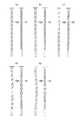
図2(a)〜図2(e)に、単独の螺旋形状のバネ部を有する比較例のバレル10Aの撓み量と、二重螺旋形状のバネ部を有するバレル10の撓み量とを、FEM解析によって比較した例を示す。比較は、バレル10とバレル10Aのそれぞれを所定の長さ(以下において「ストローク量」という。)だけ縮めることによって行った。 2A to 2E, the deflection amount of the
図2(a)は、ストローク量が0である状態を示している。バレル10とバレル10Aの長さは、それぞれ8mmである。 FIG. 2A shows a state where the stroke amount is zero. Each of the
図2(b)〜図2(e)は、ストローク量がそれぞれ10μm、20μm、30μm、40μmである状態を示す。図2(b)〜図2(e)に示すように、二重螺旋形状のバネ部を有するバレル10では、ストローク量が大きくなるに従って、両端部の中間を中心に素線の間隔が広がるが、撓み量は小さい。一方、比較例のバレル10では、ストローク量が大きくなるに従って撓み量が大きくなる。 FIG. 2B to FIG. 2E show states where the stroke amounts are 10 μm, 20 μm, 30 μm, and 40 μm, respectively. As shown in FIGS. 2 (b) to 2 (e), in the
上記のように、バネ部を多重螺旋形状にすることによって、バレル10の撓み量を低減することができる。また、比較例では一定の方向に大きく撓みが発生するが、多重螺旋形状のバネ部を有するバレル10では、応力方向が分散されて、複数の方向にそれぞれ小さな撓みが生じている。つまり、バネ部を多重螺旋形状にすることにより、撓みの大きさや方向を制御できる。 As described above, the amount of deflection of the
上記に説明したように、本発明の第1の実施形態に係るプローブでは、バレル10のバネ部を多重螺旋形状にすることにより、検査時のODやプリロードなどに起因するプローブの撓みを制御できる。その結果、図1に示したプローブによれば、プローブ間の隣接ショートの発生を抑制することができる。 As described above, in the probe according to the first embodiment of the present invention, the bending of the probe due to OD or preload at the time of inspection can be controlled by forming the spring portion of the
(第2の実施形態)
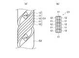
図3に示す本発明の第2の実施形態に係るプローブは、バレル10のバネ部の多重螺旋形状を構成するコイルバネの1つが、他のコイルバネよりも放熱性を高くした放熱用コイルバネC1である。例えば、放熱用コイルバネC1に、他のコイルバネC2の材料よりも熱伝導率が高い材料を使用する。(Second Embodiment)
In the probe according to the second embodiment of the present invention shown in FIG. 3, one of the coil springs constituting the multiple spiral shape of the spring portion of the
プローブの使用時には、プローブを介して被検査体に電流が流れる。このときプローブに発生するジュール熱によって、バレル10に形成したバネ部にヘタリ(熱ヘタリ)が生じることが想定される。バネ部にヘタリが生じると、被検査体やランドに接触するプローブの針圧が低下し、プローブの許容電流値が低下する。これにより、検査に必要な大きさの電流を被検査体に流すことができなくなり、被検査体の十分な検査ができない事態が生じ得る。 When the probe is used, an electric current flows through the probe through the probe. At this time, due to the Joule heat generated in the probe, it is assumed that the spring portion formed in the
これに対し、第2の実施形態に係るプローブによれば、バレル10のバネ部が放熱用コイルバネC1を有することにより、放熱用コイルバネC1を熱伝導経路としてジュール熱がバネ部の外部に速やかに放熱される。このため、バネ部の温度上昇が抑制され、ヘタリが発生しない。従って、プローブの許容電流値は低下しない。 On the other hand, according to the probe according to the second embodiment, the spring portion of the
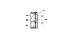
放熱用コイルバネC1には、例えば図4(a)及び図4(b)に示すように、導電性を有する基体11と、基体11よりも熱伝導率の高い材料からなり、基体11に接触する放熱材12とを有する構造などを採用可能である。図4(b)に示す放熱材12は、基体11に周囲を囲まれて基体11の内部に埋め込まれている。放熱用コイルバネC1では、バネ部に配置された放熱材12が熱伝導経路となり、バネ部に生じるジュール熱を熱伝導によってバネ部の外部に放熱する。 For example, as shown in FIGS. 4A and 4B, the heat dissipation coil spring C1 is made of a
なお、被検査体の検査時に電流をバレル10に流すため、放熱材12が導電性を有することが好ましい。例えば、放熱材12には、金(Au)、銀(Ag),銅(Cu)、アルミニウム(Al)などが好適に使用される。基体11には、Niなどが好適に使用される。バネ部の全体を導電性の材料にすることにより、プローブの許容電流値が増大する。 In addition, in order to flow an electric current through the
図4(a)に示したバレルでは、バネ部の中央に1つの帯状の放熱材12を配置した例を示したが、放熱材12の配置方法はこれに限られない。例えば、延伸方向と垂直な幅方向に互いに離間して配置された複数列の放熱材12を、放熱用コイルバネC1の延伸方向に沿って基体11の内部に配列してもよい。或いは、複数の放熱材12を基体11の膜厚方向に積層してもよい。 In the barrel shown in FIG. 4A, an example in which one belt-like
なお、放熱材12の材料は基体11よりも熱伝導率の高い材料であるが、更に、放熱材12の硬度を基体11の硬度よりも高くしてもよい。例えば、バレル10の基体11がNiである場合に、Niよりも硬度の高い材料の放熱材12を使用する。これにより、バレル10の剛性が高くなり、バネ部のヘタリを抑制することができる。その結果、プローブの許容電流値の低下を抑制できるとともに、隣接するプローブ間のショートを防止できる。 In addition, although the material of the
以上に説明したように、本発明の第2の実施形態に係るプローブでは、バネ部で発生したジュール熱が放熱用コイルバネC1を伝わって速やかにバネ部以外に放熱される。このため、バネ部の温度上昇が抑制され、バネ部のヘタリが発生しない。したがって、第2の実施形態に係るプローブによれば、プローブの撓みを制御してプローブ間の隣接ショートの発生を抑制するとともに、プローブの許容電流値の減少を抑制することができる。他は、第1の実施形態と実質的に同様であり、重複した記載を省略する。 As described above, in the probe according to the second embodiment of the present invention, Joule heat generated in the spring portion is transmitted through the heat dissipation coil spring C1 and quickly radiated to other than the spring portion. For this reason, the temperature rise of the spring portion is suppressed, and the spring portion is not set up. Therefore, according to the probe according to the second embodiment, it is possible to suppress the occurrence of an adjacent short circuit between the probes by controlling the bending of the probe and to suppress the decrease in the allowable current value of the probe. Others are substantially the same as those in the first embodiment, and redundant description is omitted.
<第1の変形例>
図5(a)及び図5(b)に示す本発明の第2の実施形態の第1の変形例に係るプローブでは、放熱用コイルバネC1の基体11に埋め込まれた放熱材12の一部が、バレル10の表面に露出している。つまり、放熱材12の全体が基体11に囲まれていない点が図4(a)及び図4(b)に示したプローブと異なる。<First Modification>
In the probe according to the first modification of the second embodiment of the present invention shown in FIGS. 5A and 5B, a part of the
図5(a)及び図5(b)に示したプローブでは、基体11に埋め込まれた放熱材12が、放熱用コイルバネC1の延伸方向に沿って螺旋状に配置されている。放熱用コイルバネC1の表面に放熱材12を露出させることにより、バネ部で生じたジュール熱を効率よくプローブの周囲に放熱させることができる。 In the probes shown in FIGS. 5A and 5B, the
図5(a)及び図5(b)では放熱材12が連続的に配置されている例を示した。しかし、放熱用コイルバネC1の延伸方向に沿って複数の放熱材12を離間して配列してもよい。 5A and 5B show an example in which the
或いは、図6(a)及び図6(b)に示すように、基体11の内部に埋め込まれた放熱材12と、一部がバレル10の表面に露出した放熱材12とを、基体11の膜厚方向に積層してもよい。図6(a)に示した例では、それぞれの放熱材12が放熱用コイルバネC1の延伸方向に沿って配置されている。 Alternatively, as shown in FIGS. 6A and 6B, the
本発明の第2の実施形態の第1の変形例に係るプローブによれば、放熱用コイルバネC1において放熱材12の一部をバネ部の表面に露出させることにより、バネ部で発生したジュール熱をプローブの周囲に効率的に放熱することができる。 According to the probe according to the first modification of the second embodiment of the present invention, Joule heat generated in the spring portion is obtained by exposing a part of the
<第2の変形例>
図7(a)及び図7(b)に示す第2の実施形態の第2の変形例に係るプローブでは、放熱材12が、基体11の表面に全体が露出して配置されている。つまり、放熱材12が基体11に埋め込まれた部分を有さない点が第1の変形例と異なる。<Second Modification>
In the probe according to the second modification of the second embodiment shown in FIGS. 7A and 7B, the
図7(a)及び図7(b)には、放熱用コイルバネC1の外部に向いた外表面にのみ放熱材12を配置する例を示した。しかし、基体11の周囲を囲むように、放熱用コイルバネC1の側面にも放熱材12を配置してもよい。 FIG. 7A and FIG. 7B show an example in which the
第2の実施形態の第2の変形例に係るプローブによれば、放熱材12を基体11の表面に配置することによって、バネ部で生じたジュール熱をプローブの周囲に速やかに放熱することができる。このため、バネ部のヘタリが発生せず、プローブの許容電流値の減少を抑制することができる。 According to the probe according to the second modification of the second embodiment, by disposing the
<第3の変形例>
本発明の第2の実施形態の第3の変形例に係るプローブは、図8(a)及び図8(b)に示すように、放熱材12が、基体11の表面に全体が露出して配置された表面領域121、及び、表面領域121と一部が接触して基体11に埋め込まれた埋込領域122を有する。つまり、基体11に埋め込まれた放熱材12とバレル10の表面に配置された放熱材12とが一体化されている。<Third Modification>
In the probe according to the third modification of the second embodiment of the present invention, as shown in FIGS. 8A and 8B, the
放熱材12の表面領域121と埋込領域122は、放熱用コイルバネC1の延伸方向に沿って螺旋状に延伸して配置されている。なお、平行に延伸する複数の埋込領域122を基体11に埋め込んだ構成にしてもよい。例えば図9に示した放熱用コイルバネC1では、2列の埋込領域122が配置されている。また、基体11の周囲を囲むように、放熱用コイルバネC1の側面から外表面に渡って連続的に表面領域121が配置されている。 The
第2の実施形態の第3の変形例に係るプローブによれば、バレル10のバネ部の内部で発生したジュール熱を、速やかにバネ部以外に放熱することができる。 According to the probe according to the third modification of the second embodiment, the Joule heat generated inside the spring portion of the
なお、上記では多重螺旋形状を構成する各コイルバネの素線の線径が同一である例を示したが、素線の線径が互いに異なってもよい。例えば、放熱用コイルバネC1の線径を他のコイルバネよりも広くすることにより、放熱性が向上する。また、放熱用コイルバネC1を、他のコイルバネC2の材料よりも熱伝導率が高い材料で形成してもよい。例えば、放熱用コイルバネC1の材料にAu、Ag、Cu、Alなどを使用し、その他のコイルバネC2の材料にNiなどを使用する。 In the above description, an example in which the wire diameters of the coil springs constituting the multiple spiral shape are the same is shown, but the wire diameters of the wire may be different from each other. For example, heat dissipation is improved by making the wire diameter of the coil spring C1 for heat dissipation wider than that of other coil springs. Further, the heat dissipating coil spring C1 may be formed of a material having a higher thermal conductivity than other coil springs C2. For example, Au, Ag, Cu, Al or the like is used as the material of the heat dissipating coil spring C1, and Ni or the like is used as the material of the other coil spring C2.
(第3の実施形態)
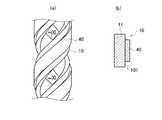
本発明の第3の実施形態に係るプローブは、図10に示すように、バレル10のバネ部の最も外側に絶縁材料からなる絶縁層40が配置されている。このため、仮に隣接するプローブ同士が接触しても、プローブ同士は絶縁層40によって電気的に絶縁されるためにプローブ間のショートを抑制できる。他は、図1に示したプローブと同様である。(Third embodiment)
In the probe according to the third embodiment of the present invention, as shown in FIG. 10, an insulating
例えば図11(a)〜図11(b)に示すように、バネ部の外側に向いた外表面101のみに絶縁層40を配置する。或いは、図12(a)〜図12(b)に示すように、コイルバネの外表面101と側面102に絶縁層40を配置してもよい。なお、図12(a)〜図12(b)は、放熱材12を基体11の内部に埋め込んだ放熱用コイルバネC1とその他のコイルバネC2に絶縁層40を配置した例である。 For example, as shown in FIGS. 11A to 11B, the insulating
図11(a)に示す構造によれば、バネ部に絶縁層40を容易に形成することができる。一方、図12(a)に示す構造によれば、より確実にプローブ間のショートを抑制できる。 According to the structure shown in FIG. 11A, the insulating
なお、図7や図8に示すプローブのように基体11の表面に放熱材12が配置される場合には、放熱材12の外側に絶縁層40を配置する。他は、第1〜第2の実施形態と実質的に同様であり、重複した記載を省略する。 When the
(その他の実施形態)
上記のように本発明は実施形態によって記載したが、この開示の一部をなす論述及び図面はこの発明を限定するものであると理解すべきではない。この開示から当業者には様々な代替実施形態、実施例及び運用技術が明らかとなろう。(Other embodiments)
As described above, the present invention has been described according to the embodiments. However, it should not be understood that the descriptions and drawings constituting a part of this disclosure limit the present invention. From this disclosure, various alternative embodiments, examples and operational techniques will be apparent to those skilled in the art.
例えば、上記ではバレル10が二重螺旋形状のバネ部を有する場合を説明したが、バネ部が3重以上の螺旋形状であってもよい。その場合、第2の実施形態の係るプローブにおいては、少なくともコイルバネの1つを、他のコイルバネよりも放熱性が高く構成された放熱用コイルバネにする。 For example, although the case where the
また、上記ではバレル10の両端部にプランジャー20が装着されたプローブの例を説明したが、バレル10の一方の端部のみにプランジャー20が装着され、バレル10の他方の端部がランドなどに接触するプローブにも、本発明は適用可能である。 Further, in the above description, an example of the probe in which the
このように、本発明はここでは記載していない様々な実施形態などを含むことはもちろんである。したがって、本発明の技術的範囲は上記の説明から妥当な特許請求の範囲に係る発明特定事項によってのみ定められるものである。 As described above, the present invention naturally includes various embodiments that are not described herein. Therefore, the technical scope of the present invention is defined only by the invention specifying matters according to the scope of claims reasonable from the above description.
10…バレル
11…基体
12…放熱材
20…プランジャー
30…接合部
40…絶縁層
C1…放熱用コイルバネDESCRIPTION OF
Claims (11)
Translated fromJapanese前記バレルの端部の開口端から先端部が露出した状態で前記バレルに接合された棒形状のプランジャーと
を備え、
前記バネ部が、中心軸が同一のコイルバネをそれぞれ構成する複数の素線からなる多重螺旋形状であることを特徴とするプローブ。A tube-shaped barrel having a spring portion formed without a plurality of spiral cuts penetrating the side surfaces; and
A rod-shaped plunger joined to the barrel with the tip exposed from the open end of the end of the barrel; and
The probe according to claim 1, wherein the spring portion has a multiple spiral shape composed of a plurality of strands constituting coil springs having the same central axis.
導電性を有する基体と、
前記基体よりも熱伝導率の高い材料からなり、前記基体に接触する放熱材と
を有することを特徴とする請求項3に記載のプローブ。The heat dissipating coil spring is
A conductive substrate;
The probe according to claim 3, further comprising: a heat dissipation material made of a material having a higher thermal conductivity than the base, and being in contact with the base.
Priority Applications (1)
| Application Number | Priority Date | Filing Date | Title |
|---|---|---|---|
| JP2017161169AJP6969930B2 (en) | 2017-08-24 | 2017-08-24 | probe |
Applications Claiming Priority (1)
| Application Number | Priority Date | Filing Date | Title |
|---|---|---|---|
| JP2017161169AJP6969930B2 (en) | 2017-08-24 | 2017-08-24 | probe |
Publications (2)
| Publication Number | Publication Date |
|---|---|
| JP2019039756Atrue JP2019039756A (en) | 2019-03-14 |
| JP6969930B2 JP6969930B2 (en) | 2021-11-24 |
Family
ID=65727525
Family Applications (1)
| Application Number | Title | Priority Date | Filing Date |
|---|---|---|---|
| JP2017161169AActiveJP6969930B2 (en) | 2017-08-24 | 2017-08-24 | probe |
Country Status (1)
| Country | Link |
|---|---|
| JP (1) | JP6969930B2 (en) |
Cited By (1)
| Publication number | Priority date | Publication date | Assignee | Title |
|---|---|---|---|---|
| KR102202827B1 (en)* | 2020-10-27 | 2021-01-14 | (주) 네스텍코리아 | Probe pin and coaxial probe assembly using the same |
Citations (10)
| Publication number | Priority date | Publication date | Assignee | Title |
|---|---|---|---|---|
| JP3090950U (en)* | 2002-06-24 | 2003-01-10 | 株式会社精研 | Measuring probe |
| US20070197099A1 (en)* | 2006-02-17 | 2007-08-23 | Centipede Systems, Inc. | High Performance Electrical Connector |
| US20070269999A1 (en)* | 2006-05-18 | 2007-11-22 | Centipede Systems, Inc. | Socket for an electronic device |
| US7491069B1 (en)* | 2008-01-07 | 2009-02-17 | Centipede Systems, Inc. | Self-cleaning socket for microelectronic devices |
| JP2010281583A (en)* | 2009-06-02 | 2010-12-16 | Nidec-Read Corp | Inspection jig |
| WO2011122068A1 (en)* | 2010-03-30 | 2011-10-06 | 住友電気工業株式会社 | Contact probe, contact probe connecting body and methods for manufacturing same |
| JP2012220451A (en)* | 2011-04-13 | 2012-11-12 | Seiken Co Ltd | Inspection unit |
| JP2013024689A (en)* | 2011-07-20 | 2013-02-04 | Micronics Japan Co Ltd | Probe allowing electric signals to pass, electric connecting device using the same, and probe manufacturing method |
| JP2015148561A (en)* | 2014-02-07 | 2015-08-20 | 株式会社日本マイクロニクス | Contact inspection apparatus |
| WO2016155936A2 (en)* | 2015-03-31 | 2016-10-06 | Feinmetall Gmbh | Method for producing at least one spring contact pin or a spring contact pin arrangement, and corresponding devices |
- 2017
- 2017-08-24JPJP2017161169Apatent/JP6969930B2/enactiveActive
Patent Citations (10)
| Publication number | Priority date | Publication date | Assignee | Title |
|---|---|---|---|---|
| JP3090950U (en)* | 2002-06-24 | 2003-01-10 | 株式会社精研 | Measuring probe |
| US20070197099A1 (en)* | 2006-02-17 | 2007-08-23 | Centipede Systems, Inc. | High Performance Electrical Connector |
| US20070269999A1 (en)* | 2006-05-18 | 2007-11-22 | Centipede Systems, Inc. | Socket for an electronic device |
| US7491069B1 (en)* | 2008-01-07 | 2009-02-17 | Centipede Systems, Inc. | Self-cleaning socket for microelectronic devices |
| JP2010281583A (en)* | 2009-06-02 | 2010-12-16 | Nidec-Read Corp | Inspection jig |
| WO2011122068A1 (en)* | 2010-03-30 | 2011-10-06 | 住友電気工業株式会社 | Contact probe, contact probe connecting body and methods for manufacturing same |
| JP2012220451A (en)* | 2011-04-13 | 2012-11-12 | Seiken Co Ltd | Inspection unit |
| JP2013024689A (en)* | 2011-07-20 | 2013-02-04 | Micronics Japan Co Ltd | Probe allowing electric signals to pass, electric connecting device using the same, and probe manufacturing method |
| JP2015148561A (en)* | 2014-02-07 | 2015-08-20 | 株式会社日本マイクロニクス | Contact inspection apparatus |
| WO2016155936A2 (en)* | 2015-03-31 | 2016-10-06 | Feinmetall Gmbh | Method for producing at least one spring contact pin or a spring contact pin arrangement, and corresponding devices |
Cited By (1)
| Publication number | Priority date | Publication date | Assignee | Title |
|---|---|---|---|---|
| KR102202827B1 (en)* | 2020-10-27 | 2021-01-14 | (주) 네스텍코리아 | Probe pin and coaxial probe assembly using the same |
Also Published As
| Publication number | Publication date |
|---|---|
| JP6969930B2 (en) | 2021-11-24 |
Similar Documents
| Publication | Publication Date | Title |
|---|---|---|
| KR102498454B1 (en) | Contact probe and inspection jig | |
| US11131690B2 (en) | Contact probe for testing head | |
| TWI482974B (en) | Contact probe and socket | |
| KR101408550B1 (en) | Contact terminal for a probe card, and the probe card | |
| KR102015798B1 (en) | Probe for the test device | |
| TWI682180B (en) | Electrical connection device | |
| JP2017078660A (en) | Probe card and contact inspection device | |
| JP5624740B2 (en) | Contact probe and socket | |
| JP2013190270A (en) | Probe and connection jig | |
| WO2012067126A1 (en) | Contact probe and probe unit | |
| KR101729069B1 (en) | A probe having a barrel with heat release holes | |
| JP2019090760A (en) | Probe head | |
| US11828773B2 (en) | Electrical connecting device | |
| TW201538984A (en) | Contact inspection device | |
| JP2016008904A (en) | Contact probe | |
| TW200935068A (en) | Contact probe | |
| JP2015004614A (en) | Contact probe | |
| JP2019039756A (en) | probe | |
| JP4916719B2 (en) | Contact probe and contact probe mounting structure | |
| US10401388B2 (en) | Probe card device and rectangular probe thereof | |
| KR102234964B1 (en) | Probe | |
| US20190086443A1 (en) | Probe card device and round probe thereof | |
| JP6961422B2 (en) | probe | |
| WO2020026409A1 (en) | Contact probe and test socket equipped with same | |
| JP6889067B2 (en) | Electrical connection device |
Legal Events
| Date | Code | Title | Description |
|---|---|---|---|
| A621 | Written request for application examination | Free format text:JAPANESE INTERMEDIATE CODE: A621 Effective date:20200616 | |
| A977 | Report on retrieval | Free format text:JAPANESE INTERMEDIATE CODE: A971007 Effective date:20210405 | |
| A131 | Notification of reasons for refusal | Free format text:JAPANESE INTERMEDIATE CODE: A131 Effective date:20210422 | |
| A521 | Request for written amendment filed | Free format text:JAPANESE INTERMEDIATE CODE: A523 Effective date:20210607 | |
| TRDD | Decision of grant or rejection written | ||
| A01 | Written decision to grant a patent or to grant a registration (utility model) | Free format text:JAPANESE INTERMEDIATE CODE: A01 Effective date:20211019 | |
| A61 | First payment of annual fees (during grant procedure) | Free format text:JAPANESE INTERMEDIATE CODE: A61 Effective date:20211028 | |
| R150 | Certificate of patent or registration of utility model | Ref document number:6969930 Country of ref document:JP Free format text:JAPANESE INTERMEDIATE CODE: R150 | |
| R250 | Receipt of annual fees | Free format text:JAPANESE INTERMEDIATE CODE: R250 |