JP2019034465A - Thermal head - Google Patents
Thermal headDownload PDFInfo
- Publication number
- JP2019034465A JP2019034465AJP2017156788AJP2017156788AJP2019034465AJP 2019034465 AJP2019034465 AJP 2019034465AJP 2017156788 AJP2017156788 AJP 2017156788AJP 2017156788 AJP2017156788 AJP 2017156788AJP 2019034465 AJP2019034465 AJP 2019034465A
- Authority
- JP
- Japan
- Prior art keywords
- thermal head
- driving
- input terminal
- driver
- resistor
- Prior art date
- Legal status (The legal status is an assumption and is not a legal conclusion. Google has not performed a legal analysis and makes no representation as to the accuracy of the status listed.)
- Granted
Links
Images


Landscapes
- Electronic Switches (AREA)
Abstract
Description
Translated fromJapanese本発明は、サーマルヘッドに関する。 The present invention relates to a thermal head.
従来、多数の発熱体と、各発熱体を独立して発熱させる印字信号を与える個別電極および共通電極と、個別電極に接続されて各発熱体に流れる電流の通電、非通電を制御する駆動ICと、駆動ICの信号入力端子に接続された配線パターンと、共通電極に接続された配線パターンとが設けられたサーマルヘッドが知られている(例えば、特許文献1)。 Conventionally, a large number of heating elements, individual electrodes and common electrodes for providing a print signal for independently heating each heating element, and a drive IC that is connected to the individual electrodes and controls energization and non-energization of the current flowing through each heating element There is known a thermal head provided with a wiring pattern connected to a signal input terminal of a driving IC and a wiring pattern connected to a common electrode (for example, Patent Document 1).
従来のサーマルヘッドには、機械に組み込む際の接続ケーブルのハンドリング等により駆動ICの信号入力端子に接続された配線パターンと共通電極に接続された配線パターンとが短絡すると、駆動ICが破損するおそれがあった。 In a conventional thermal head, if the wiring pattern connected to the signal input terminal of the driving IC and the wiring pattern connected to the common electrode are short-circuited due to handling of the connection cable when incorporated in the machine, the driving IC may be damaged. was there.
第1の態様によると、サーマルヘッドは、絶縁基板上に形成され駆動電圧が印加された共通電極と、前記絶縁基板上に形成された複数の個別電極と、回路基板上に設けられ、制御信号に基づき前記複数の個別電極の各々に流れる電流を制御して発熱体への通電、非通電を制御する駆動ICと、前記回路基板上に設けられ、外部から前記駆動電圧が入力される電圧入力端子と、前記回路基板上に設けられ外部から前記制御信号が入力される、前記駆動ICと電気的に接続された信号入力端子と、前記絶縁基板上に形成され、前記信号入力端子と前記駆動ICとを接続する抵抗と、を備える。 According to the first aspect, the thermal head is provided on the circuit board, the common electrode formed on the insulating substrate and applied with the driving voltage, the plurality of individual electrodes formed on the insulating substrate, and the control signal. A drive IC for controlling energization / non-energization to the heating element by controlling a current flowing through each of the plurality of individual electrodes, and a voltage input provided on the circuit board and receiving the drive voltage from the outside A terminal, a signal input terminal electrically connected to the drive IC, which is provided on the circuit board and receives the control signal from the outside, and formed on the insulating substrate, the signal input terminal and the drive And a resistor for connecting the IC.
本発明によれば、駆動ICの破損を防止することができる。 According to the present invention, it is possible to prevent the drive IC from being damaged.
(第1の実施の形態)
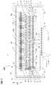
図1は、本発明の第1の実施の形態に係るサーマルヘッドの構成を示す平面図である。図2は、図1のI−I線断面を模式的に示す図である。サーマルヘッド100は、支持板5上に固定された絶縁基板4およびプリント配線板等の回路基板9を備える。絶縁基板4およびプリント配線板等の回路基板9は、粘着層11によって支持板5上に固定されている。(First embodiment)
FIG. 1 is a plan view showing the configuration of the thermal head according to the first embodiment of the present invention. FIG. 2 is a diagram schematically showing a cross section taken along line II of FIG. The
絶縁基板4は、セラミックなどの絶縁体によって形成される。絶縁基板4上には、例えば金などの導体をフォトリソグラフィ法を用いて、不要な部分をエッチングにより除去することで、共通電極2、複数の個別電極3、抵抗部50が形成されている。共通電極2、複数の個別電極3、および抵抗部50の上方(図1の紙面上方向)には、例えば厚膜印刷により、帯状の発熱体1が形成されている。個別電極3の一部、共通電極2の一部、および抵抗部50の一部は、それぞれ保護膜12により被覆される。保護膜12は、例えばガラス等により構成される。
なお、抵抗部50は本実施形態の特徴的構成要素であり、後で詳細に説明する。The insulating
The
プリント配線板等の回路基板9には、ドライバIC6a、ドライバIC6b、およびコネクタ10が設けられている。ドライバIC6a、ドライバIC6bはそれぞれ、複数の個別電極3に接続されて各発熱体1に流れる電流の通電、非通電を制御するCMOS構造を有する駆動ICであり、以下の説明において、ドライバIC6aおよびドライバIC6bをドライバIC6と総称する。コネクタ10は、印字制御等を行う外部機器にサーマルヘッド100を接続するための接続部材である。各々の個別電極3の一端は、いずれかのドライバIC6に金線等の金属線7aで接続されている。金線等の金属線7aおよびドライバIC6は、封止樹脂8によりモールドされている。なお、後述する金線7b〜7dも封止樹脂8によりモールドされている。 A
共通電極2は、共通電極基部21および複数の共通電極延在部20を有する。共通電極基部21は、矩形の絶縁基板4が有する4辺のうち、プリント配線板9に面した1辺を除く3つの辺に沿って、発熱体1を取り囲むように形成されている。複数の共通電極延在部20は、図1において発熱体1と平行に延在する共通電極基部21の一領域から副走査方向42(図1の紙面上下方向)に沿って延在する。後述するように、発熱体1の延在方向は主走査方向である。
複数の個別電極3はそれぞれ、接続部32、個別電極延在部30、および個別電極パッド31を有する。個別電極延在部30は、共通電極2の一対の共通電極延在部20の間に位置し副走査方向42に沿って延在する。接続部32は、個別電極延在部30の基端側端部から副走査方向42に延在する。The
Each of the plurality of
個別電極パッド31は、接続部32の他端、すなわち個別電極延在部30とは反対側の接続部32の端部に設けられている。つまり、接続部32の一端には個別電極延在部30が設けられ、他端には個別電極パッド31が設けられている。換言すると、個別電極延在部30と個別電極パッド31は接続部32で接続されている。 The
複数の共通電極延在部20と複数の個別電極延在部30は、交互に対向してかみ合うように形成されている。発熱体1は、複数の共通電極延在部20と複数の個別電極延在部30に跨がって、言い換えると横断して形成され、共通電極延在部20と個別電極延在部30の配列方向である主走査方向41(図1の紙面左右方向)に延設されている。 The plurality of common
複数の個別電極パッド31は、絶縁基板4のプリント配線板等の回路基板9側の縁部4a(図1,図2)に沿って、すなわち主走査方向41に沿って、所定ピッチで一列に配列されている。ドライバIC6は、上面視が細長い矩形形状(全体として細長い四角柱)であり、長手方向をプリント配線板9側の縁部4aの延在方向に整列させてプリント配線板等の回路基板9にダイボンディングされている。ドライバIC6の上面には、絶縁基板4に対向する縁部に沿って、すなわち主走査方向41に沿って、複数のIC電極パッド60aが形成されている。複数の個別電極パッド31は、複数のIC電極パッド60aと同一のピッチで配列されている。1つのIC電極パッド60aには、1つの個別電極パッド31が対応する。各々の個別電極パッド31は、金線等の金属線7aによって、対応するIC電極パッド60aと電気的に接続されている。
ドライバIC6はさらに、入力電極パッド60bおよび出力電極パッド60cを有する。ドライバIC6aの入力電極パッド60bは、金線等の金属線7dにより抵抗部50に接続されている。ドライバIC6aのシリアルデータをドライバIC6bにデイジーチェーン接続するための出力電極パッド60cは、金線等の金属線7eにより絶縁基板4に設けられた電極パッド31aに接続され、金線等の金属線7fにより主走査方向に電気的に接続された同じく電極パッド31bを介してドライバIC6bの入力電極パッド60bに接続されている。The plurality of
The
絶縁基板4の一部領域は、図1に一点鎖線で示す保護膜12により被覆される。保護膜12により保護される領域には、発熱体1と、共通電極2の少なくとも共通電極延在部20を含む大部分と、個別電極3のうち個別電極パッド31を除く部分(すなわち個別電極延在部30および接続部32の大部分)と、抵抗部50の一部と、が含まれる。換言すると、これらの部材が保護膜12で保護される。 A partial region of the
2つのドライバIC6a,6bは、共通電極2から発熱体1を介して各々の個別電極3に電流を流す。これにより、共通電極延在部20と個別電極延在部30とが交互に対向してかみ合う様に形成された部分の間にある発熱体1部分に電流が流れ、その部分が発熱する。この熱を感熱紙などの印字媒体に与えることで印字が行われる。 The two
本実施の形態に係るサーマルヘッド100の主走査方向41における印刷解像度は、例えば約203dpiである。この場合、主走査方向41における、印字されるドットの幅は125μmになる。すなわち、主走査方向41における共通電極延在部20の配列ピッチおよび個別電極延在部30の配列ピッチは、125μmである。 The print resolution in the
本実施の形態に係るサーマルヘッド100が有するドライバIC6は、1つあたり192個の個別電極3を制御する。
なお、図1では、作図の都合上、個別電極3を実際よりも少なく簡略化して図示している。そのため、共通電極延在部20の個数、個別電極延在部30の個数、個別電極パッド31の個数、IC電極パッド60aの個数、入力電極パッドの個数なども、実際よりも少なく図示している。The
In FIG. 1, for convenience of drawing, the
本実施の形態に係るサーマルヘッド100の、主走査方向41における個別電極パッド31の配列ピッチおよびIC電極パッド60aの配列ピッチは、例えば63μmである。すなわち、主走査方向41における共通電極延在部20および個別電極延在部30の配列ピッチ44,45は、主走査方向41における個別電極パッド31およびIC電極パッド60aの配列ピッチ46,47よりも大きい。 In the
配列ピッチに差があることから、複数の個別電極3は、ドライバIC6との相対的な位置関係に応じて、異なる形状を有している。例えばドライバIC6の中央に近い個別電極3aは、一端に設けられた個別電極延在部30から、他端に設けられた個別電極パッド31まで、副走査方向にほぼ平行に直線的な形状を有している。一方、ドライバIC6の端に近い個別電極3bは、一端に設けられた個別電極延在部30から、他端に設けられた個別電極パッド31まで、非直線的な形状、すなわち屈曲形状を有している。具体的には、1つのドライバIC6に対応する複数の個別電極3は、発熱体1側からドライバIC6に向かって、全体として細くすぼまっている。 Since there is a difference in arrangement pitch, the plurality of
図1に示す実施形態では、N個の発熱体1を2分してドライバIC6a,6bでそれぞれN/2個の発熱体1を駆動制御する。その結果、個別電極3は、ドライバIC6aに対応する左側の接続部群32Lと、ドライバIC6bに対応する右側の接続部群32Rとに2分される。 In the embodiment shown in FIG. 1,
右側の接続部群32Rを構成する複数の接続部32の中央の接続部3aは、ほぼ副走査方向と平行に延在している。中央の接続部3aから左右に並ぶ複数の接続部32の延在方向は、左右端に近いものほど大きく屈曲している。換言すると、傾斜角が大きくされている。したがって、接続部32の副走査方向の延在距離、すなわち電気経路長は左端の接続部3bと右端の接続部3cが中央の接続部3aに比べて長い、すなわち抵抗値が大きい。なお、左側の接続部群32Lについても同様である。 A central connection portion 3a of the plurality of
プリント配線板等の回路基板9の図1における下部には、すなわちプリント配線板9の絶縁基板4側とは逆側の縁には、コネクタ10と電気的に接続される複数の端子13が一列に並べて配置されている。左端の端子13aは共通電極2に電源を印加する端子であり、共通配線パターン2Aに接続されている。共通配線パターン2Aの他端は、金線7bを介して、絶縁基板4上の共通電極2と電気的に接続されている。端子13aには、コネクタ10を介して、サーマルヘッド100の外部から例えば24V程度の駆動電圧が入力される。すなわち端子13aは、駆動電圧が入力される電圧入力端子である。駆動電圧は、共通電極2に印加される電圧である。 A plurality of terminals 13 electrically connected to the
端子13aの隣に配置される端子13bは、個別電極3に対する電流の通電/非通電を制御するための端子である。端子13bは個別配線パターン3Aに接続され、個別配線パターン3Aの他端は、金線等の金属線7cを介して、絶縁基板4上に形成された抵抗部50と電気的に接続されている。抵抗部50は、金線等の金属線7dにより、ドライバIC6aの入力電極パッド60bと電気的に接続されている。端子13bには、コネクタ10を介して、サーマルヘッド100の外部から制御信号が入力される。すなわち端子13bは、制御信号が入力される信号入力端子である。ドライバIC6aは、入力電極パッド60bに入力された制御信号やその他の制御信号に基づき、ドライバIC6aと接続される個別電極3の電流を制御する。制御信号は、例えば0V〜5Vの範囲の中で電圧を、High、Lowの2値に定義されている。 The terminal 13b disposed next to the terminal 13a is a terminal for controlling current application / non-energization with respect to the
ドライバIC6aは、入力されたシリアルデータを出力電極パッド60cから順次出力する。シリアルデータはドライバIC6aの出力電極パッド60cから絶縁基板4上の個別電極パッド31aに金線等の金属線7eを介して接続し、主走査方向に電気的に接続された同じく個別電極パッド31bからドライバIC6b上の入力電極パッド60bに金線等の金属線7fによりに接続される。つまり、ドライバIC6aとドライバIC6bは金線等の金属線7e,7fと絶縁基板上の配線によりいわゆるデイジーチェーン接続されている。 The
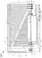
図3は、抵抗部50の構成を模式的に示す平面図である。抵抗部50は、図3において絶縁基板4の左下コーナ部に設けられている。詳細には、絶縁基板4の左下コーナ部において、絶縁基板4の左縁に設けられている共通電極基部21と、最左端に位置する個別電極3の接続部32bとに囲まれた三角形形状の領域に形成されている。抵抗部50は、共通電極2の基部21および個別電極3と同一の材料(例えば金など)を用いて、共通電極2の基部21および個別電極3と同一のプロセスにより形成される。 FIG. 3 is a plan view schematically showing the configuration of the
抵抗部50は、一端51と、他端53と、一端51および他端53を接続する接続部52とから成る。一端51は、プリント配線板等の回路基板9上の個別配線パターン3Aを介して端子13bに電気的に接続されている。他端53は、ドライバIC6aの入力電極パッド60bに電気的に接続されている。接続部52は、絶縁基板4上の保護膜12により被覆された領域に、一端51と他端53とを接続する長大な配線として形成される。実施形態における抵抗部50の接続部52は折り返しパターン、ジグザグパターン、繰り返しパターンなど呼ぶことができる。このようなパターンを採用することにより、狭い三角形形状の領域内で長い配線長を実現し、抵抗部50を所望の抵抗値、例えば30〜300Ω程度の電気抵抗値を得ている。 The
図4は、ドライバIC6aおよびその周辺の回路図である。ドライバIC6aはCMOS構造を有する。ドライバIC6aの入力電極パッド60bに対して、各発熱体に接続されるIC電極パッド60aは、いわゆるオープンドレイン端子として機能する。端子13bから入力された制御信号は、抵抗部50を介して、ドライバIC6aの入力電極パッド60bに入力される。ドライバIC6aは、ダイオード63、ダイオード64、および制御部65を有する。入力電極パッド60bは、ダイオード63のアノード、ダイオード64のカソード、および制御部65に接続される。ダイオード63のカソードは、例えば5Vの電源VDDに接続される。ダイオード64のアノードはGNDであり基準電位となる。 FIG. 4 is a circuit diagram of the
制御部65は、入力された制御信号に基づいてIC電極パッド60aの電位をスイッチング制御することにより、そのIC電極パッド60aに対応する個別電極3に流れる電流を制御する。これにより、各々の個別電極3に対応する発熱体1の各ドット1a、1b、1c、…に流れる電流がオンオフされ、所望の印刷結果が得られる。 The
例えばコネクタ10にワイヤーハーネスを斜めに差し込んでしまう等の理由により、端子13aと端子13bとが短絡してしまった場合、抵抗部50がなければ(端子13bと入力電極パッド60bとが直結されていれば)、駆動電圧が入力電極パッド60bに印加されることになる。制御信号の電圧は例えば5V程度であるのに対して、駆動電圧の電圧はそれより高く、例えば24V程度であり、各発熱体1を介してオープンドレイン端子60aに接続されているため、入力電極パッド60bには過電流が流れ込んでしまう。これにより、通常CMOSで構成された制御部65の耐圧はVDDによる電位で支配されるため、例えばVDDが5V仕様の場合でも入力電極パッド60bに24Vの電位が印加されると、ダイオード63の能力以上の電流が流れるために、そのジュール熱により内部配線が焼失するなど、、ドライバIC6aが破損するおそれがある。
本実施の形態に係るサーマルヘッド100は、抵抗部50を有しているので、端子13aと端子13bとが短絡してしまった場合であっても、抵抗部50により入力電極パッド60bに流れ込む電流は制限され、ダイオード63の保護機能が継続されることになる。For example, when the terminal 13a and the terminal 13b are short-circuited due to, for example, the wire harness being inserted into the
Since the
また、入力電極パッド60bに5V以上の電圧が印加されようとする場合であっても、ダイオード63により入力電極パッド60bの電位は電源VDDと同一になるので、抵抗部50において電流が消費され、制御部65に過大な電圧が印加されることもなければドライバIC6aのジュール熱による破損も抑制される。つまりダイオード63は、ドライバIC6aを過電圧から保護するクランプダイオードとして機能する。 Even when a voltage of 5 V or more is about to be applied to the
上述した実施の形態によれば、次の作用効果が得られる。
(1)外部から制御信号が入力される端子13bとドライバIC6aとを直結する代わりに、抵抗部50が、端子13bとドライバIC6aとを接続するようにした。従って、外部から駆動電圧が入力される端子13aが、端子13bと短絡してしまった場合であっても、ドライバIC6aの瞬時に電流が流れることによる破損を防止することができる。According to the embodiment described above, the following operational effects can be obtained.
(1) Instead of directly connecting the terminal 13b to which the control signal is input from the outside and the
(2)プリント配線板等の回路基板9に配置された複数の端子13において、端子13aと端子13bは隣接している。例えば、端子13に電気的に接続されるケーブルがFFCあるいはFPCであった場合、FFCあるいはFPC側の電気的接続を取るための隣接した接続端子の間にはガイドが存在していない。したがって、端子13側のコネクタのハウジング部とFFCあるいはFPCの端子方向の長さ寸法の相対関係で、前記ハウジング部の端子13の並び方向の両端で間隙が生ずる場合がある。前記間隙は、FFCあるいはFPCが斜めに差し込まれて端子13aと端子13bが短絡する危険性を引き起こすことになり、FFCあるいはFPCの接続端子列のピッチが狭くなればなるほど前記危険性は高まることになる。本実施の形態では、抵抗部50を設けたので、FFCあるいはFPCが斜めに差し込まれて端子13aと端子13bが短絡してしまった場合であっても、ドライバIC6aが破損しない。(2) In the plurality of terminals 13 arranged on the
(3)抵抗部50を、絶縁基板4上に配線パターンとして形成したので、サーマルヘッド100の組み立ての際に追加の部品を必要としない。(3) Since the
(4)抵抗部50を、共通電極2および個別電極3と同一の材料により形成したので、共通電極2および複数の個別電極3と同一プロセスで抵抗部50を一体的に形成することができ、抵抗部50のための追加の工程を必要としない。(4) Since the
(5)抵抗部50を、絶縁基板4上のコーナ部において、共通電極2と個別電極3とで囲まれた領域に設けた。このように、絶縁基板4上の空きスペースを有効利用することができるので、抵抗部50のために絶縁基板4のサイズを変更する必要がない。(5) The
(6)ドライバIC6aを動作させるための電源VDDと抵抗部50との間にクランプダイオードとして機能するダイオード63を設けたので、ドライバIC6aに過電圧が印加されそうになった場合であっても、電流は電源VDDに向けて流れるので過電圧が印加されない。つまり、ドライバIC6aが過電圧から保護される。(6) Since the
(7)ドライバIC6は複数設けられ、各ドライバIC6には制御信号が入力される入力電極パッド60bおよび制御信号を出力する出力電極パッド60cを有する。ドライバIC6aとドライバIC6bは、入力電極パッド60bおよび出力電極パッド60cにより絶縁基板4を介してデイジーチェーン接続される。このように、複数のドライバIC6を絶縁基板4を介してデイジーチェーン接続することで、プリント配線板等回路基板9に新たな配線や、金線等の金属線を接続するためのスペースが不要となり、プリント配線板等回路基板9の短手のサイズを縮小化することができる。(7) A plurality of
(8)ダイオード63をドライバIC6a内に設けたので、絶縁基板4やプリント配線板等回路基板9に余分なスペースを設ける必要がない。
(9)同様のメカニズムにより抵抗部50を接続したドライバIC6の入力端子は静電気耐性を向上することができる。実験的には2倍以上の静電気耐性の向上が観測されている。(8) Since the
(9) The input terminal of the
次のような変形も本発明の範囲内であり、変形例の一つ、もしくは複数を上述の実施形態と組み合わせることも可能である。
(変形例1)
ドライバIC6aだけでなく、ドライバIC6bにもダイオード63を内蔵させてよい。つまりドライバIC6aとドライバIC6bの構成が同一であってもよい。このようにすることで、サーマルヘッド100を構成する部品の品種数を減らすことができ、サーマルヘッド100の製造難度を低減することができる。また、サーマルヘッド100の量産効果が高まる。The following modifications are also within the scope of the present invention, and one or a plurality of modifications can be combined with the above-described embodiment.
(Modification 1)
The
(変形例2)
ダイオード63は、ドライバIC6aの外部に設けてもよい。このようにすることで、ドライバIC6aの構造が単純化されるので、ドライバIC6aのコストを削減することができる。また、この場合、ダイオード63は、ダイオード自身の降伏電圧を利用して使用するツェナーダイオードであってもよい。(Modification 2)
The
(変形例4)
抵抗部50を配線パターンとして形成するのではなく、例えばチップ抵抗やカーボン抵抗などの部品により構成してもよい。このようにすることで、抵抗部50の抵抗値をより高くすることができる。また、抵抗部50に加えて、追加の抵抗をドライバIC6a内の入力電極パッド60bと制御部65との間に設けることでも、同様の効果を得ることができる。更には、絶縁基板上の抵抗部50を発熱体1と同じ材料で形成しても良い。(Modification 4)
Instead of forming the
(変形例5)
ドライバIC6の個数は2個でなくてもよい。例えば、ドライバIC6を1個だけにしてもよいし、ドライバIC6を3個以上用いてもよい。ドライバIC6を3個以上用いる場合には、それら全てをデイジーチェーン接続してよい。このように、2個ではない数のドライバIC6を設けた場合であっても、上述した実施の形態と同様の作用効果が得られる。(Modification 5)
The number of
上記では、種々の実施の形態および変形例を説明したが、本発明はこれらの内容に限定されるものではない。本発明の技術的思想の範囲内で考えられるその他の態様も本発明の範囲内に含まれる。 Although various embodiments and modifications have been described above, the present invention is not limited to these contents. Other embodiments conceivable within the scope of the technical idea of the present invention are also included in the scope of the present invention.
100…サーマルヘッド、1…発熱体、2…共通電極、3…個別電極、4…絶縁基板、6、6a、6b…ドライバIC、7、7a、7b、7c、7d、14…金線、9…プリント配線板、12…保護膜、13、13a、13b…端子、20…共通電極延在部、30…個別電極延在部、31…個別電極パッド、60a…IC電極パッド、60b…入力電極パッド、60c…出力電極パッドDESCRIPTION OF
Claims (8)
Translated fromJapanese前記絶縁基板上に形成された複数の個別電極と、
回路基板上に設けられ、制御信号に基づき前記複数の個別電極の各々に流れる電流を制御して発熱体への通電、非通電を制御する駆動ICと、
前記回路基板上に設けられ、外部から前記駆動電圧が入力される電圧入力端子と、
前記回路基板上に設けられ外部から前記制御信号が入力される、前記駆動ICと電気的に接続された信号入力端子と、
前記絶縁基板上に形成され、前記信号入力端子と前記駆動ICとを接続する抵抗と、
を備えるサーマルヘッド。A common electrode formed on an insulating substrate and applied with a driving voltage;
A plurality of individual electrodes formed on the insulating substrate;
A driving IC provided on the circuit board and controlling the current flowing through each of the plurality of individual electrodes based on a control signal to control energization and de-energization of the heating element;
A voltage input terminal provided on the circuit board, to which the drive voltage is input from the outside;
A signal input terminal electrically connected to the driving IC, which is provided on the circuit board and receives the control signal from the outside;
A resistor formed on the insulating substrate and connecting the signal input terminal and the driving IC;
Thermal head equipped with.
前記回路基板には、前記電圧入力端子および前記信号入力端子を含む複数の入力端子が配置され、
前記電圧入力端子および前記信号入力端子は隣接しているサーマルヘッド。The thermal head according to claim 1,
A plurality of input terminals including the voltage input terminal and the signal input terminal are disposed on the circuit board,
The voltage input terminal and the signal input terminal are adjacent thermal heads.
前記抵抗は、前記絶縁基板上に形成された配線パターンであるサーマルヘッド。The thermal head according to claim 1 or 2,
The resistor is a thermal head that is a wiring pattern formed on the insulating substrate.
前記抵抗は、前記共通電極および前記個別電極の少なくとも一方と同一の材料により形成されているサーマルヘッド。In the thermal head according to claim 3,
The resistor is a thermal head formed of the same material as at least one of the common electrode and the individual electrode.
前記抵抗は、前記絶縁基板上のコーナ部において、前記共通電極と前記個別電極とで囲まれた領域に設けられているサーマルヘッド。In the thermal head according to claim 3 or claim 4,
The resistor is a thermal head provided in a region surrounded by the common electrode and the individual electrode in a corner portion on the insulating substrate.
前記駆動ICを動作させるための電圧源と前記抵抗との間であって、前記駆動ICが有する前記抵抗に接続された入力電極の近傍に設けられたダイオードを更に備えるサーマルヘッド。In the thermal head according to any one of claims 1 to 5,
A thermal head further comprising a diode provided between a voltage source for operating the driving IC and the resistor and in the vicinity of an input electrode connected to the resistor of the driving IC.
前記駆動ICは複数設けられ、各駆動ICには前記制御信号が入力される入力端子および前記制御信号を出力する出力端子を有し、前記複数の駆動ICは、前記入力端子および前記出力端子によりデイジーチェーン接続されているサーマルヘッド。The thermal head according to claim 6,
A plurality of the driving ICs are provided, and each driving IC has an input terminal for inputting the control signal and an output terminal for outputting the control signal, and the plurality of driving ICs are provided by the input terminal and the output terminal. Thermal head connected in daisy chain.
前記ダイオードは、少なくとも1つの前記駆動IC内に設けられ、
前記1つの駆動ICの前記入力端子には、前記抵抗が接続されるサーマルヘッド。
In the thermal head according to claim 7,
The diode is provided in at least one of the driving ICs,
A thermal head to which the resistor is connected to the input terminal of the one drive IC.
Priority Applications (1)
| Application Number | Priority Date | Filing Date | Title |
|---|---|---|---|
| JP2017156788AJP6754339B2 (en) | 2017-08-15 | 2017-08-15 | Thermal head |
Applications Claiming Priority (1)
| Application Number | Priority Date | Filing Date | Title |
|---|---|---|---|
| JP2017156788AJP6754339B2 (en) | 2017-08-15 | 2017-08-15 | Thermal head |
Publications (2)
| Publication Number | Publication Date |
|---|---|
| JP2019034465Atrue JP2019034465A (en) | 2019-03-07 |
| JP6754339B2 JP6754339B2 (en) | 2020-09-09 |
Family
ID=65636565
Family Applications (1)
| Application Number | Title | Priority Date | Filing Date |
|---|---|---|---|
| JP2017156788AActiveJP6754339B2 (en) | 2017-08-15 | 2017-08-15 | Thermal head |
Country Status (1)
| Country | Link |
|---|---|
| JP (1) | JP6754339B2 (en) |
Cited By (3)
| Publication number | Priority date | Publication date | Assignee | Title |
|---|---|---|---|---|
| JP2020192346A (en)* | 2010-04-29 | 2020-12-03 | ジンテス ゲゼルシャフト ミット ベシュレンクテル ハフツング | Orthognathic implant |
| US11357514B2 (en) | 2010-04-29 | 2022-06-14 | DePuy Synthes Products, Inc. | Orthognathic implant and methods of use |
| JP2023068486A (en)* | 2021-11-02 | 2023-05-17 | ローム株式会社 | thermal print head |
Citations (10)
| Publication number | Priority date | Publication date | Assignee | Title |
|---|---|---|---|---|
| JPS58122401U (en)* | 1982-02-12 | 1983-08-20 | 松下電器産業株式会社 | Low resistance chip resistor for small power applications |
| JPH01192158A (en)* | 1988-01-28 | 1989-08-02 | Sumitomo Electric Ind Ltd | Input protective circuit of semiconductor device |
| JPH02214151A (en)* | 1989-02-15 | 1990-08-27 | Olympus Optical Co Ltd | Input protective circuit of semiconductor device |
| JPH049749U (en)* | 1990-05-16 | 1992-01-28 | ||
| US5389953A (en)* | 1991-01-02 | 1995-02-14 | Eastman Kodak Company | Non-impact printer module with improved burn-in testing capability and method using same |
| JPH10138542A (en)* | 1996-09-12 | 1998-05-26 | Aoi Denshi Kk | Thermal head |
| JP2002079707A (en)* | 2000-05-29 | 2002-03-19 | Kyocera Corp | Light-emitting array, optical printer head using the light-emitting element array and method for driving optical printer head |
| JP2010194856A (en)* | 2009-02-25 | 2010-09-09 | Kyocera Corp | Recording head and recording apparatus equipped with the same |
| JP2011201184A (en)* | 2010-03-26 | 2011-10-13 | Kyocera Corp | Thermal head |
| JP2013147025A (en)* | 2011-12-22 | 2013-08-01 | Kyocera Corp | Thermal head and thermal printer provided with the same |
- 2017
- 2017-08-15JPJP2017156788Apatent/JP6754339B2/enactiveActive
Patent Citations (10)
| Publication number | Priority date | Publication date | Assignee | Title |
|---|---|---|---|---|
| JPS58122401U (en)* | 1982-02-12 | 1983-08-20 | 松下電器産業株式会社 | Low resistance chip resistor for small power applications |
| JPH01192158A (en)* | 1988-01-28 | 1989-08-02 | Sumitomo Electric Ind Ltd | Input protective circuit of semiconductor device |
| JPH02214151A (en)* | 1989-02-15 | 1990-08-27 | Olympus Optical Co Ltd | Input protective circuit of semiconductor device |
| JPH049749U (en)* | 1990-05-16 | 1992-01-28 | ||
| US5389953A (en)* | 1991-01-02 | 1995-02-14 | Eastman Kodak Company | Non-impact printer module with improved burn-in testing capability and method using same |
| JPH10138542A (en)* | 1996-09-12 | 1998-05-26 | Aoi Denshi Kk | Thermal head |
| JP2002079707A (en)* | 2000-05-29 | 2002-03-19 | Kyocera Corp | Light-emitting array, optical printer head using the light-emitting element array and method for driving optical printer head |
| JP2010194856A (en)* | 2009-02-25 | 2010-09-09 | Kyocera Corp | Recording head and recording apparatus equipped with the same |
| JP2011201184A (en)* | 2010-03-26 | 2011-10-13 | Kyocera Corp | Thermal head |
| JP2013147025A (en)* | 2011-12-22 | 2013-08-01 | Kyocera Corp | Thermal head and thermal printer provided with the same |
Cited By (4)
| Publication number | Priority date | Publication date | Assignee | Title |
|---|---|---|---|---|
| JP2020192346A (en)* | 2010-04-29 | 2020-12-03 | ジンテス ゲゼルシャフト ミット ベシュレンクテル ハフツング | Orthognathic implant |
| US11357514B2 (en) | 2010-04-29 | 2022-06-14 | DePuy Synthes Products, Inc. | Orthognathic implant and methods of use |
| US12433605B2 (en) | 2010-04-29 | 2025-10-07 | DePuy Synthes Products, Inc. | Orthognathic implant and methods of use |
| JP2023068486A (en)* | 2021-11-02 | 2023-05-17 | ローム株式会社 | thermal print head |
Also Published As
| Publication number | Publication date |
|---|---|
| JP6754339B2 (en) | 2020-09-09 |
Similar Documents
| Publication | Publication Date | Title |
|---|---|---|
| JP6754339B2 (en) | Thermal head | |
| JP2012158034A (en) | Thermal head | |
| JP7310082B2 (en) | Driver IC for thermal print head and thermal print head | |
| JP5385456B2 (en) | Thermal head | |
| CN109383133B (en) | Thermal head | |
| JP7230666B2 (en) | Driver IC for thermal print head, thermal print head, and wiring pattern of thermal print head | |
| JP5489836B2 (en) | Thermal head | |
| JP7581000B2 (en) | Thermal printhead, its manufacturing method, and thermal printer | |
| CN109484036B (en) | Thermal head | |
| US6392685B1 (en) | Drive IC chip and printhead | |
| JP6208561B2 (en) | Thermal head and thermal printer | |
| JP3483890B2 (en) | Printer drive IC and print head using the same | |
| JP5511510B2 (en) | Thermal head | |
| JP2016137692A (en) | Thermal head and thermal printer comprising the same | |
| JP7680828B2 (en) | Thermal printhead, its manufacturing method, and thermal printer | |
| JPH10315518A (en) | Thermal head | |
| JP5260038B2 (en) | Thermal print head and manufacturing method thereof | |
| JP6689116B2 (en) | Thermal print head and thermal printer | |
| JPH0939284A (en) | Line type thermal printing head | |
| JPH10138542A (en) | Thermal head | |
| JP2019059119A (en) | Thermal print head and thermal printer | |
| JP2023114780A (en) | Thermal print head and thermal printer | |
| JP5511507B2 (en) | Thermal head | |
| JP2002052753A (en) | Thermal print head | |
| JP2005225054A (en) | Thermal head and its wiring method, and drive unit for thermal head |
Legal Events
| Date | Code | Title | Description |
|---|---|---|---|
| A621 | Written request for application examination | Free format text:JAPANESE INTERMEDIATE CODE: A621 Effective date:20190423 | |
| A977 | Report on retrieval | Free format text:JAPANESE INTERMEDIATE CODE: A971007 Effective date:20200228 | |
| A131 | Notification of reasons for refusal | Free format text:JAPANESE INTERMEDIATE CODE: A131 Effective date:20200310 | |
| A521 | Request for written amendment filed | Free format text:JAPANESE INTERMEDIATE CODE: A523 Effective date:20200414 | |
| TRDD | Decision of grant or rejection written | ||
| A01 | Written decision to grant a patent or to grant a registration (utility model) | Free format text:JAPANESE INTERMEDIATE CODE: A01 Effective date:20200804 | |
| A61 | First payment of annual fees (during grant procedure) | Free format text:JAPANESE INTERMEDIATE CODE: A61 Effective date:20200821 | |
| R150 | Certificate of patent or registration of utility model | Ref document number:6754339 Country of ref document:JP Free format text:JAPANESE INTERMEDIATE CODE: R150 | |
| R250 | Receipt of annual fees | Free format text:JAPANESE INTERMEDIATE CODE: R250 | |
| R250 | Receipt of annual fees | Free format text:JAPANESE INTERMEDIATE CODE: R250 | |
| R250 | Receipt of annual fees | Free format text:JAPANESE INTERMEDIATE CODE: R250 |