JP2019016496A - Organic el display panel and manufacturing method of organic el display panel - Google Patents
Organic el display panel and manufacturing method of organic el display panelDownload PDFInfo
- Publication number
- JP2019016496A JP2019016496AJP2017132646AJP2017132646AJP2019016496AJP 2019016496 AJP2019016496 AJP 2019016496AJP 2017132646 AJP2017132646 AJP 2017132646AJP 2017132646 AJP2017132646 AJP 2017132646AJP 2019016496 AJP2019016496 AJP 2019016496A
- Authority
- JP
- Japan
- Prior art keywords
- electrode layer
- layer
- auxiliary electrode
- power supply
- supply auxiliary
- Prior art date
- Legal status (The legal status is an assumption and is not a legal conclusion. Google has not performed a legal analysis and makes no representation as to the accuracy of the status listed.)
- Granted
Links
Images


Landscapes
- Devices For Indicating Variable Information By Combining Individual Elements (AREA)
- Electroluminescent Light Sources (AREA)
Abstract
Translated fromJapaneseDescription
Translated fromJapanese本開示は、有機材料の電界発光現象を利用した有機EL(Electro Luminescence)素子を用いた有機EL表示パネル及びその製造方法に関する。 The present disclosure relates to an organic EL display panel using an organic EL (Electro Luminescence) element using an electroluminescence phenomenon of an organic material, and a manufacturing method thereof.
近年、デジタルテレビ等の表示装置に用いられる表示パネルとして、基板上に有機EL素子をマトリックス状に複数配列した有機EL表示パネルが実用化されている。
有機EL表示パネルでは、一般に各有機EL素子の発光層と、隣接する有機EL素子とは絶縁材料からなる絶縁層で仕切られており、カラー表示用の有機EL表示パネルにおいては、有機EL素子がRGB各色に発光する副画素を形成し、隣り合うRGBの副画素が組合わさってカラー表示における単位画素が形成されている。In recent years, an organic EL display panel in which a plurality of organic EL elements are arranged in a matrix on a substrate has been put into practical use as a display panel used in a display device such as a digital television.
In the organic EL display panel, the light emitting layer of each organic EL element and the adjacent organic EL element are generally partitioned by an insulating layer made of an insulating material. In the organic EL display panel for color display, the organic EL element is Sub-pixels that emit light of RGB colors are formed, and adjacent RGB sub-pixels are combined to form a unit pixel in color display.
有機EL素子は、一対の電極の間に有機発光材料を含む発光層が配設された基本構造を有し、駆動時には、一対の電極対間に電圧を印加し、発光層に注入されるホールと電子との再結合に伴って発光する。
トップエミッション型の有機EL素子は、基板上に画素電極、有機層(発光層を含む)、及び共通電極が順に設けられた素子構造を有する。発光層からの光は、光反射性材料からなる画素電極にて反射されるとともに、光透光性材料からなる共通電極から上方に出射される。共通電極は、基板上の表示画素部全面にわたって成膜することが多い。テレビ等大画面表示装置への利用に向けた有機EL表示パネルが大型化に伴い、共通電極の電気抵抗が増加し、給電部から遠い部分では電圧降下により電流が十分に供給されずに発光効率が低下し、これに起因して輝度ムラが発生することが懸念される。An organic EL element has a basic structure in which a light emitting layer containing an organic light emitting material is disposed between a pair of electrodes, and when driven, a hole is injected into the light emitting layer by applying a voltage between the pair of electrodes. Emits light upon recombination of electrons with electrons.
A top emission type organic EL element has an element structure in which a pixel electrode, an organic layer (including a light emitting layer), and a common electrode are sequentially provided on a substrate. The light from the light emitting layer is reflected by the pixel electrode made of a light reflective material and emitted upward from the common electrode made of a light transmissive material. In many cases, the common electrode is formed over the entire surface of the display pixel portion on the substrate. With the increase in size of organic EL display panels for use in large-screen display devices such as televisions, the electrical resistance of the common electrode increases, and current is not sufficiently supplied due to voltage drop in areas far from the power supply unit, resulting in luminous efficiency There is a concern that the brightness may be reduced and luminance unevenness may occur due to this.
これに対し、例えば、特許文献1では、基板上の画素電極と同層に補助電極層を延伸し、その上に共通電極を重畳させて共通電極との電気的な接続を図ることにより、共通電極の電気抵抗を低減する技術が提案されている。また、補助電極層と共通電極とを金属酸化物からなるホール注入層を介して積層して、補助電極層と共通電極との電気的な接続を図る技術(例えば、特許文献2)や、金属原子を含む電子輸送層を介して積層する技術が提案されている(例えば、特許文献3)。 On the other hand, for example, in
ところが、補助電極層の材料に画素電極と同じ光反射性を有するアルミニウム、銀といった金属を用いた場合、その後の製造工程において補助電極層の表層に酸化膜が形成され、補助電極層と共通電極層と間の接触電気抵抗が高まるという課題があった。
本開示は、上記課題に鑑みてなされたものであり、補助電極層に画素電極と同じ光反射性を有する安価な金属材料を用いた構成において、共通電極層と補助電極層との間の電気的接続における接触電気抵抗の低減を図り、発光効率を向上させるとともに輝度ムラを抑制する有機EL表示パネル、及びその有機EL表示パネルの製造方法を提供することを目的とする。However, when a metal such as aluminum or silver having the same light reflectivity as the pixel electrode is used as the material of the auxiliary electrode layer, an oxide film is formed on the surface layer of the auxiliary electrode layer in the subsequent manufacturing process, and the auxiliary electrode layer and the common electrode are formed. There was a problem that the contact electrical resistance between the layers increased.
The present disclosure has been made in view of the above-described problems. In a configuration in which an inexpensive metal material having the same light reflectivity as that of the pixel electrode is used for the auxiliary electrode layer, electricity between the common electrode layer and the auxiliary electrode layer is provided. An object of the present invention is to provide an organic EL display panel that reduces the contact electrical resistance in a general connection, improves luminous efficiency, and suppresses uneven luminance, and a method for manufacturing the organic EL display panel.
上記目的を達成するため、本開示の一態様に係る有機EL表示パネルは、基板上に複数の画素電極が行列状に配され、各画素電極上に有機発光材料を含む発光層が配されてなる有機EL表示パネルであって、基板と、前記基板の上方に行列状に配された複数の画素電極と、前記基板の上方において、隣接する前記画素電極の間隙のうちの少なくとも1の間隙内に列又は行方向に延伸して配された第1給電補助電極層と、前記第1給電補助電極層に重畳して配された第2給電補助電極層と、前記複数の画素電極上に配された複数の発光層と、前記複数の発光層の上方、前記第1給電補助電極層及び前記第2給電補助電極層を覆って連続して配された共通電極層とを備え、前記第1給電補助電極層と前記共通電極層とは、少なくとも前記第1給電補助電極層の上面に垂直な壁面上の一部領域において接しており、前記第2給電補助電極層は、アルミニウムを主成分として含み、かつ、少なくとも前記第2給電補助電極層の表層にはアルミニウムの酸化物が形成されており、前記第1給電補助電極層は、アルミニウムと異なる金属を主成分として含み、アルミニウムよりも大気中における接触抵抗が低い材料からなることを特徴とする。 In order to achieve the above object, an organic EL display panel according to one embodiment of the present disclosure includes a plurality of pixel electrodes arranged in a matrix on a substrate, and a light-emitting layer including an organic light-emitting material disposed on each pixel electrode. An organic EL display panel comprising: a substrate; a plurality of pixel electrodes arranged in a matrix above the substrate; and at least one gap among gaps between adjacent pixel electrodes above the substrate A first power supply auxiliary electrode layer disposed extending in the column or row direction, a second power supply auxiliary electrode layer disposed so as to overlap the first power supply auxiliary electrode layer, and the plurality of pixel electrodes. A plurality of light emitting layers, and a common electrode layer continuously disposed above the plurality of light emitting layers and covering the first power supply auxiliary electrode layer and the second power supply auxiliary electrode layer, The auxiliary power supply electrode layer and the common electrode layer include at least the first electric power supply. The second power supply auxiliary electrode layer is in contact with a part of the wall surface perpendicular to the upper surface of the auxiliary electrode layer, the second power supply auxiliary electrode layer contains aluminum as a main component, and at least the surface layer of the second power supply auxiliary electrode layer is made of aluminum. The first feeding auxiliary electrode layer is made of a material containing a metal different from aluminum as a main component and having a lower contact resistance in the atmosphere than aluminum.
本開示の一態様に係る有機EL表示パネルは、補助電極層に画素電極と同じ光反射性を有する安価な金属材料を用いた構成において、共通電極層と補助電極層との間の電気的接続における接触電気抵抗を低減することができる。その結果、発光効率を向上させると共に輝度ムラを抑制することができる。 An organic EL display panel according to one embodiment of the present disclosure has an electrical connection between a common electrode layer and an auxiliary electrode layer in a configuration using an inexpensive metal material having the same light reflectivity as a pixel electrode for the auxiliary electrode layer. The contact electrical resistance at can be reduced. As a result, it is possible to improve luminous efficiency and suppress luminance unevenness.
≪発明を実施するための形態に至った経緯≫
トップエミッション型の有機EL素子は、厚みを最適に設定して光共振器構造を採用することにより出射される光の色度を調整し輝度を高めているため、画素電極の表面部が高い光反射性を有することが必要である。そのため、画素電極には、金属層、合金層、透明導電膜層などが選択され、金属層としては、シート抵抗が小さく、高い光反射性を有する材料として、例えば、銀(Ag)又はアルミニウム(Al)を含む金属材料から構成することができる。このうち、材料コストを考慮すると銀よりも工業的にはアルミニウムを選択することが好ましい。≪Background to the form for carrying out the invention≫
The top-emission type organic EL device uses an optical resonator structure with an optimal thickness to adjust the chromaticity of the emitted light and increase the brightness. It is necessary to have reflectivity. Therefore, a metal layer, an alloy layer, a transparent conductive film layer, or the like is selected for the pixel electrode. As the metal layer, a material having a low sheet resistance and high light reflectivity, such as silver (Ag) or aluminum ( It can be composed of a metal material containing Al). Among these, in consideration of material cost, it is preferable to select aluminum industrially than silver.
他方、給電補助電極層は、基板上の画素電極と同時に同層に形成されるために、画素電極と同じ材料により形成される。したがって、補助電極層には、アルミニウムを主成分として含む金属層、合金層を用いることとなる。しかしながら、この場合、補助電極層の製膜後に行われる上層の製造工程において補助電極層の表層に酸化膜が形成され、補助電極層と共通電極層と間の接触電気抵抗が高くなることが発明者らの検討により判明した。その理由は、補助電極層よりも後に形成されるホール注入層やバンクの焼成工程、ウェットプロセスなどにおいて補助電極層のアルミニウムを主成分として含む金属層、又は合金層が酸化するためであると考えられる。 On the other hand, since the auxiliary power supply electrode layer is formed in the same layer as the pixel electrode on the substrate, it is formed of the same material as the pixel electrode. Therefore, a metal layer or an alloy layer containing aluminum as a main component is used for the auxiliary electrode layer. However, in this case, an oxide film is formed on the surface of the auxiliary electrode layer in the upper layer manufacturing process performed after the auxiliary electrode layer is formed, and the contact electric resistance between the auxiliary electrode layer and the common electrode layer is increased. It became clear by examination of those. The reason is considered to be that the metal layer or alloy layer containing aluminum as a main component of the auxiliary electrode layer is oxidized in the hole injection layer formed after the auxiliary electrode layer, the firing process of the bank, the wet process, or the like. It is done.
特に、特許文献2に記載されるような金属酸化物(例えば、酸化タングステン:WOx)からなるホール注入層を介した状態で補助電極層と共通電極とを積層して、補助電極層と共通電極との電気的な接続を図る場合には、ホール注入層の介在により補助電極層と共通電極との接触電気抵抗が増加するのみならず、補助電極層のアルミニウム合金がより酸化しやすい状態になることが発明者らの検討により判明した。一般に、ITOに対し良好な接触電機抵抗が得られると報告されているアルミニウム合金を補助電極層の材料に用いた場合でも、アルミの酸化膜被膜が補助電極表面に形成され、共通電極との接触電機抵抗が増加することが発明者らの実験により判明している。その理由は、酸化タングステン自体に含まれる酸素が補助電極層に移動しやすいこと、あるいは、酸化タングステンは空孔密度が他材料に比べて高いことから、ウェット工程や焼成工程において上層からの現像液などの薬液や水の浸透、またはベーク時に酸素を通過させやすいために補助電極層に酸素が進入しやすいことなどが影響、起因していると考えられる。 In particular, the auxiliary electrode layer and the common electrode are stacked by interposing the auxiliary electrode layer and the common electrode through a hole injection layer made of a metal oxide (for example, tungsten oxide: WOx) as described in
そして、補助電極層のアルミニウム合金が酸化した場合、補助電極層中に欠陥や異物などの存在により局所的に酸化膜を介さずに補助電極層と共通電極とが電気的に接続された場合、その部位に電流が集中して流れ局所的な発熱や材料劣化などが発生するおそれがあることがわかった。
さらに、特許文献3に記載されるように、発光素子部分におけるキャリア移動度を増加する目的で、高抵抗なフッ化物と金属原子を含む電子輸送層を介して補助電極層と共通電極を積層する構成も提案されている。しかしながら、補助電極層と共通電極間では、画素電極と共通電極間とは電気的極性が逆になることから、高抵抗なフッ化物と金属原子を含むものの金属層そのものではない電子輸送層が介在することにより補助電極層と共通電極との接触電気抵抗がさらに増加することとなる。キャリア移動度をさらなる向上のために電子輸送層の膜厚増加も考慮すべきである。And when the aluminum alloy of the auxiliary electrode layer is oxidized, when the auxiliary electrode layer and the common electrode are electrically connected without locally passing through the oxide film due to the presence of defects or foreign matters in the auxiliary electrode layer, It has been found that current concentrates on the part and local heat generation or material deterioration may occur.
Further, as described in Patent Document 3, for the purpose of increasing the carrier mobility in the light emitting element portion, the auxiliary electrode layer and the common electrode are stacked via the electron transport layer containing a high resistance fluoride and a metal atom. A configuration is also proposed. However, between the auxiliary electrode layer and the common electrode, the electrical polarity is reversed between the pixel electrode and the common electrode, so an electron transport layer that contains high resistance fluoride and metal atoms but is not the metal layer itself is interposed. As a result, the contact electric resistance between the auxiliary electrode layer and the common electrode is further increased. In order to further improve the carrier mobility, an increase in the thickness of the electron transport layer should be considered.
これに対し、特許文献4では、補助電極層と対向電極間に発光機能層が介在する構成において、断面視したとき補助電極層は側面において電子輸送層を介さずに対向電極と接触する有機EL素子が提案されている。しかしながら、この構成では、上述のとおり、補助電極層の表層に酸化膜が形成された場合には、補助電極層と対向電極と間の接触電気抵抗が高くなることが懸念される。 On the other hand, in Patent Document 4, in the configuration in which the light emitting functional layer is interposed between the auxiliary electrode layer and the counter electrode, the auxiliary electrode layer is in contact with the counter electrode on the side surface without the electron transport layer when viewed in cross section. Devices have been proposed. However, in this configuration, as described above, when an oxide film is formed on the surface layer of the auxiliary electrode layer, there is a concern that the contact electric resistance between the auxiliary electrode layer and the counter electrode is increased.
そこで、発明者らは、補助電極層に画素電極と同じ光反射性を有する安価な金属材料を用いた構成において、共通電極層と補助電極層との間の電気的接続における接触電気抵抗を低減できる構成について鋭意検討を行い、以下の実施の形態に至った。
≪本発明を実施するための形態の概要≫
本開示の態様に係る有機EL表示パネルは、有機EL表示パネルは、基板上に複数の画素電極が行列状に配され、各画素電極上に有機発光材料を含む発光層が配されてなる有機EL表示パネルであって、基板と、前記基板の上方に行列状に配された複数の画素電極と、前記基板の上方において、隣接する前記画素電極の間隙のうちの少なくとも1の間隙内に列又は行方向に延伸して配された第1給電補助電極層と、前記第1給電補助電極層に重畳して配されたアルミニウムを主成分として含む第2給電補助電極層と、前記複数の画素電極上に配された複数の発光層と、前記複数の発光層の上方、前記第1給電補助電極層及び前記第2給電補助電極層を覆って連続して配された共通電極層とを備え、前記第1給電補助電極層と前記共通電極層とは、少なくとも前記第1給電補助電極層の上面に垂直な壁面上の一部領域において接触しており、前記第2給電補助電極層は、前記第1給電補助電極層は、アルミニウムと異なる金属を主成分として含み、アルミニウムよりも大気中における接触抵抗が低い材料からなることを特徴とする。Therefore, the inventors reduced the contact electric resistance in the electrical connection between the common electrode layer and the auxiliary electrode layer in a configuration using an inexpensive metal material having the same light reflectivity as the pixel electrode for the auxiliary electrode layer. The earnest examination was carried out about the structure which can be performed, and it came to the following embodiment.
<< Outline of Embodiment for Implementing the Present Invention >>
An organic EL display panel according to an aspect of the present disclosure is an organic EL display panel in which a plurality of pixel electrodes are arranged in a matrix on a substrate, and a light emitting layer containing an organic light emitting material is arranged on each pixel electrode. An EL display panel, comprising: a substrate; a plurality of pixel electrodes arranged in a matrix above the substrate; and a column in at least one of the gaps between adjacent pixel electrodes above the substrate. Alternatively, the first power supply auxiliary electrode layer arranged extending in the row direction, the second power supply auxiliary electrode layer mainly including aluminum arranged so as to overlap the first power supply auxiliary electrode layer, and the plurality of pixels A plurality of light emitting layers disposed on the electrodes, and a common electrode layer disposed continuously above the plurality of light emitting layers and covering the first power supply auxiliary electrode layer and the second power supply auxiliary electrode layer. The first power supply auxiliary electrode layer and the common electrode layer; At least in a partial region on the wall surface perpendicular to the upper surface of the first power supply auxiliary electrode layer. The second power supply auxiliary electrode layer is made of a metal different from aluminum. It is characterized by being made of a material that is contained as a component and has a lower contact resistance in air than aluminum.
また、別の態様では、上記態様において、前記第2給電補助電極層は、少なくとも前記第2給電補助電極層の表層にはアルミニウムの酸化物が形成されている構成としてもよい。
係る構成により、補助電極層に画素電極と同じ光反射性を有する安価な金属材料を用いた同層で形成した構成においても、共通電極層と補助電極層との間の電気的接続における接触電気抵抗を低減することができる。その結果、発光効率を向上させると共に輝度ムラを抑制することができる。In another aspect, in the above aspect, the second power supply auxiliary electrode layer may be configured such that an oxide of aluminum is formed on at least a surface layer of the second power supply auxiliary electrode layer.
With such a configuration, even in a configuration in which the auxiliary electrode layer is formed of the same layer using an inexpensive metal material having the same light reflectivity as that of the pixel electrode, the contact electricity in the electrical connection between the common electrode layer and the auxiliary electrode layer is achieved. Resistance can be reduced. As a result, it is possible to improve luminous efficiency and suppress luminance unevenness.
また、別の態様では、上記何れかの態様において、さらに、前記第2給電補助電極層と前記共通電極層との間には、前記複数の発光層の上方、前記第1給電補助電極層及び前記第2給電補助電極層を覆って連続して配された1層以上からなる機能層を備え、前記第1給電補助電極層の一部領域付近において、前記機能層は欠落又は薄層化しており、前記第1給電補助電極層の厚みは前記発光層上の前記機能層の厚みよりも厚い構成としてもよい。 In another aspect, in any one of the above aspects, further between the second power supply auxiliary electrode layer and the common electrode layer, above the plurality of light emitting layers, the first power supply auxiliary electrode layer, and A functional layer composed of one or more layers continuously arranged so as to cover the second power supply auxiliary electrode layer; in the vicinity of a partial region of the first power supply auxiliary electrode layer, the functional layer is missing or thinned; The thickness of the first power supply auxiliary electrode layer may be greater than the thickness of the functional layer on the light emitting layer.
係る構成により、補助電極層と共通電極とを金属酸化物(WOx)からなるホール注入層を介して積層する場合や、発光素子部分におけるキャリア移動度を増加する目的で、金属原子を含む電子輸送層を介して補助電極層と共通電極を積層する場合においても、第1給電補助電極層と共通電極層とを、少なくとも第1給電補助電極層の上面に垂直な壁面上の一部領域において接触させることができる。 With such a configuration, when an auxiliary electrode layer and a common electrode are stacked via a hole injection layer made of a metal oxide (WOx), or for the purpose of increasing carrier mobility in a light emitting element portion, electron transport including metal atoms is performed. Even when the auxiliary electrode layer and the common electrode are stacked via the layers, the first power supply auxiliary electrode layer and the common electrode layer are contacted at least in a partial region on the wall surface perpendicular to the upper surface of the first power supply auxiliary electrode layer. Can be made.
また、別の態様では、上記何れかの態様において、前記第2給電補助電極層の表層付近の抵抗は、前記第1給電補助電極層の表層付近の抵抗より高い構成としてもよい。また、別の態様では、上記何れかの態様において、前記第1給電補助電極層と前記共通電極層との間の接触抵抗は、前記第2給電補助電極層と前記共通電極層との間の接触抵抗より低い構成としてもよい。また、別の態様では、上記何れかの態様において、前記材料のシート抵抗は、アルミニウムのシート抵抗より高い構成としてもよい。 In another aspect, in any one of the above aspects, the resistance near the surface layer of the second power feeding auxiliary electrode layer may be higher than the resistance near the surface layer of the first power feeding auxiliary electrode layer. In another aspect, in any one of the above aspects, the contact resistance between the first power supply auxiliary electrode layer and the common electrode layer is between the second power supply auxiliary electrode layer and the common electrode layer. It is good also as a structure lower than contact resistance. In another aspect, in any of the above aspects, the sheet resistance of the material may be higher than the sheet resistance of aluminum.
また、別の態様では、上記何れかの態様において、前記アルミニウムと異なる金属は、タングステン、クロム、チタン、モリブデン、ニッケル、銅、ランタン、インジウムから選択される1以上の金属、またはそれらを含む金属の積層構成としてもよい。
係る構成により、これらの金属は、室温では化学的に安定しているので、第1補助電極層の表層部にはアルミニウムに比べて、金属の酸化物が形成されにくい構成とすることができる。In another aspect, in any one of the above aspects, the metal different from aluminum is one or more metals selected from tungsten, chromium, titanium, molybdenum, nickel, copper, lanthanum, and indium, or a metal including them. It is good also as a laminated structure.
With such a configuration, these metals are chemically stable at room temperature, so that a metal oxide is less likely to be formed on the surface layer portion of the first auxiliary electrode layer than aluminum.
また、別の態様では、上記何れかの態様において、前記第1給電補助電極層は、ITO又はIZOからなる構成としてもよい。
係る構成により、これらの酸化物は、室温では化学的に安定しているので、第1補助電極層の表層部には金属の酸化物が形成されにくい構成とすることができる。または、ITO、IZOなどもとから酸化物でありながら、導電性を有する構成とすることができる。そのため、大気中における接触抵抗がアルミニウムよりも低い。言い換えれば、第2給電補助電極層の表層付近の抵抗は、第1給電補助電極層の表層付近の抵抗より高い構成を実現することができる。In another aspect, in any of the above aspects, the first power feeding auxiliary electrode layer may be made of ITO or IZO.
With such a configuration, these oxides are chemically stable at room temperature, so that a metal oxide is hardly formed on the surface layer portion of the first auxiliary electrode layer. Alternatively, a conductive structure can be used while being an oxide such as ITO or IZO. Therefore, the contact resistance in the atmosphere is lower than that of aluminum. In other words, it is possible to realize a configuration in which the resistance near the surface layer of the second power feeding auxiliary electrode layer is higher than the resistance near the surface layer of the first power feeding auxiliary electrode layer.
また、別の態様では、上記何れかの態様において、前記機能層を第1の機能層とするとき、さらに、前記第2給電補助電極層と前記第1の機能層との間には、前記複数の発光層の下方、前記第1給電補助電極層及び前記第2給電補助電極層の上方に不連続に配された第2の機能層を備える構成としてもよい。
係る構成により、補助電極層と共通電極とを金属酸化物(WOx)からなるホール注入層を介して積層することができる。In another aspect, in any one of the above aspects, when the functional layer is the first functional layer, the second power feeding auxiliary electrode layer and the first functional layer further include the It is good also as a structure provided with the 2nd functional layer arrange | positioned discontinuously under the several light emitting layer and the said 1st electric power feeding auxiliary electrode layer and the said 2nd electric power feeding auxiliary electrode layer.
With this configuration, the auxiliary electrode layer and the common electrode can be stacked via the hole injection layer made of metal oxide (WOx).
また、別の態様では、上記何れかの態様において、さらに、前記第2給電補助電極層と前記機能層との間には、前記複数の発光層の下方、前記第1給電補助電極層及び前記第2給電補助電極層の上方に不連続に配されたITO又はIZOからなる透明導電層を備える構成としてもよい。
係る構成により、画素電極と共通電極との間で光共振器構造に必要な光路長を確保するための光学調整層として透明導電層を利用することができる。In another aspect, in any one of the above aspects, further between the second power supply auxiliary electrode layer and the functional layer, below the light emitting layers, the first power supply auxiliary electrode layer, and the It is good also as a structure provided with the transparent conductive layer which consists of ITO or IZO discontinuously distribute | arranged above the 2nd electric power feeding auxiliary electrode layer.
With such a configuration, a transparent conductive layer can be used as an optical adjustment layer for securing an optical path length necessary for the optical resonator structure between the pixel electrode and the common electrode.
また、別の態様では、上記何れかの態様において、前記共通電極層は、ITO又はIZOからなる透明導電層を含む構成としてもよい。
係る構成により、共通電極層をスパッタリング法により成膜することができ、第1給電補助電極層と共通電極層とを、少なくとも第1給電補助電極層の上面に垂直な壁面上の一部領域において接触させることができる。In another aspect, in any of the above aspects, the common electrode layer may include a transparent conductive layer made of ITO or IZO.
With this configuration, the common electrode layer can be formed by a sputtering method, and the first power supply auxiliary electrode layer and the common electrode layer are formed at least in a partial region on the wall surface perpendicular to the upper surface of the first power supply auxiliary electrode layer. Can be contacted.
また、別の態様では、上記何れかの態様において、前記共通電極層は、銀を主成分とする金属電極層を含む構成としてもよい。
係る構成により、共通電極層のシート抵抗を低減することができる。
また、別の態様では、上記何れかの態様において、前記基板上方に樹脂を主成分とする平坦化下部層と平坦化上部層からなる平坦化層を備え、前記平坦化下部層と前記平坦化上部層とのの間には、列又は行方向に延伸して配され、第3給電補助電極層を備え、前記平坦化上部層には前記第3給電補助電極層の上面までを貫通するコンタクトホールが開設されており、前記第1給電補助電極層が前記第3補助電極層とコンタクトホールを介して電気的に接続されており、前記共通電極層は、前記コンタクトホールに内周面と底面とに連続して配されており、前記第3給電補助電極層と前記共通電極層とは前記第1給電補助電極層を介して電気的に接続されている構成としてもよい。In another aspect, in any of the above aspects, the common electrode layer may include a metal electrode layer containing silver as a main component.
With this configuration, the sheet resistance of the common electrode layer can be reduced.
In another aspect, in any one of the above aspects, a planarization layer including a planarization lower layer mainly composed of a resin and a planarization upper layer is provided above the substrate, and the planarization lower layer and the planarization are provided. A third power supply auxiliary electrode layer is provided between the upper layer and the upper power supply layer so as to extend in the column or row direction, and the flattening upper layer penetrates up to the upper surface of the third power supply auxiliary electrode layer. A hole is opened, and the first auxiliary power supply electrode layer is electrically connected to the third auxiliary electrode layer via a contact hole, and the common electrode layer has an inner peripheral surface and a bottom surface of the contact hole. The third power supply auxiliary electrode layer and the common electrode layer may be electrically connected via the first power supply auxiliary electrode layer.
係る構成により、第3給電補助電極層の行方向断面に相当する分だけ補助電極の断面積を増加してシート抵抗を低減することができ、画素密度の増加(高精細化)に伴う光取り出し効率低下抑制できる。また、基板上の平坦化下部層と平坦化上部層との間に補助電極を設ける構成から、基板上の画素電極等による位置的制約が少なく、第3給電補助電極層の平面的なレイアウトの自由度が向上する。 With such a configuration, it is possible to increase the cross-sectional area of the auxiliary electrode by an amount corresponding to the cross-section in the row direction of the third power supply auxiliary electrode layer, thereby reducing the sheet resistance, and to extract light accompanying an increase in pixel density (high definition) Efficiency reduction can be suppressed. In addition, since the auxiliary electrode is provided between the flattening lower layer and the flattening upper layer on the substrate, there are few positional restrictions due to pixel electrodes on the substrate, and the planar layout of the third power supply auxiliary electrode layer is reduced. The degree of freedom is improved.
また、別の態様では、さらに、前記コンタクトホールの底面と前記コンタクトホール内の前記共通電極層との間には機能層が配されており、前記コンタクトホールの深さは前記機能層の厚みよりも厚く、前記第1給電補助電極層と前記共通電極層とは、少なくとも前記第1給電補助電極層における前記コンタクトホールに内周面上の一部領域において接触している構成としてもよい。 In another aspect, a functional layer is further disposed between the bottom surface of the contact hole and the common electrode layer in the contact hole, and the depth of the contact hole is greater than the thickness of the functional layer. The first power supply auxiliary electrode layer and the common electrode layer may be configured to be in contact with at least the contact hole in the first power supply auxiliary electrode layer in a partial region on the inner peripheral surface.
係る構成より、共通電極層と第1給電補助電極層との接触箇所を増加し、第3給電補助電極層への給電経路の断面積を増加することができる。その結果、共通電極層から給電補助電極への接続抵抗を低減できる。また、別の態様では、上記何れかの態様において、前記基板は、TFT基板と、TFT基板上方に樹脂を主成分とする絶縁層とを含み、前記基板上方に樹脂を主成分とする平坦化層を備え、前記TFT基板と前記絶縁層との間には、列又は行方向に延伸して配された第4給電補助電極層を備え、前記平坦化層には、当該平坦化層上面から前記第4給電補助電極層の下面までを貫通するコンタクトホールが開設されており、前記第1給電補助電極層が前記第4補助電極層と前記コンタクトホールを介して電気的に接続されており、前記共通電極層は、前記コンタクトホールに内周面と底面とに連続して配されており、前記第4給電補助電極層と前記共通電極層とは、前記第1給電補助電極層を介して電気的に接続されている構成としてもよい。 With this configuration, the number of contact points between the common electrode layer and the first power supply auxiliary electrode layer can be increased, and the cross-sectional area of the power supply path to the third power supply auxiliary electrode layer can be increased. As a result, the connection resistance from the common electrode layer to the power feeding auxiliary electrode can be reduced. In another aspect, in any one of the above aspects, the substrate includes a TFT substrate and an insulating layer mainly composed of a resin above the TFT substrate, and is planarized based on the resin above the substrate. A fourth power supply auxiliary electrode layer extending in the column or row direction between the TFT substrate and the insulating layer, and the planarizing layer includes an upper surface of the planarizing layer. A contact hole penetrating to the lower surface of the fourth power supply auxiliary electrode layer is opened, and the first power supply auxiliary electrode layer is electrically connected to the fourth auxiliary electrode layer via the contact hole; The common electrode layer is continuously arranged in the contact hole on an inner peripheral surface and a bottom surface, and the fourth power supply auxiliary electrode layer and the common electrode layer are interposed via the first power supply auxiliary electrode layer. It is good also as a structure electrically connected.
係る構成により、第4給電補助電極層の行方向断面に相当する分だけ補助電極の断面積を増加してシート抵抗を低減することができ、画素密度の増加(高精細化)に伴う光取り出し効率低下抑制できる。また、基板中のチャンネル保護層と無機絶縁層との間に補助電極を設ける構成から、基板上の画素電極等による位置的制約が少なく、第4給電補助電極層の平面的なレイアウトの自由度が向上する。 With such a configuration, the sheet resistance can be reduced by increasing the cross-sectional area of the auxiliary electrode by an amount corresponding to the cross-section in the row direction of the fourth power supply auxiliary electrode layer, and light extraction accompanying an increase in pixel density (high definition) Efficiency reduction can be suppressed. In addition, since the auxiliary electrode is provided between the channel protective layer and the inorganic insulating layer in the substrate, there are few positional restrictions due to the pixel electrode or the like on the substrate, and the degree of freedom in planar layout of the fourth power supply auxiliary electrode layer Will improve.
また、別の態様では、上記何れかの態様において、さらに、前記基板における前記コンタクトホールの底面と前記コンタクトホール内の前記共通電極層との間には機能層が配されており、前記コンタクトホールの深さは前記機能層の厚みよりも厚く、前記第1給電補助電極層と前記共通電極層とは、少なくとも前記第1給電補助電極層における前記コンタクトホールに内周面上の一部領域において接触している構成としてもよい。 In another aspect, in any one of the above aspects, a functional layer is further disposed between a bottom surface of the contact hole in the substrate and the common electrode layer in the contact hole, and the contact hole The first feed auxiliary electrode layer and the common electrode layer are at least in a partial region on the inner peripheral surface of the contact hole in the first feed auxiliary electrode layer. It is good also as a structure which is contacting.
係る構成により、共通電極層と第1給電補助電極層との接触箇所を増加し、第4給電補助電極層への給電経路の断面積を増加することができる。その結果、共通電極層から給電補助電極への接続抵抗を低減できる。
また、別の態様では、上記何れかの態様において、前記基板は、TFT基板と、TFT基板上方に樹脂を主成分とする絶縁層とを含み、前記基板上方に樹脂を主成分とする平坦下部層と平坦化上部層からなる平坦化層を備え、前記平坦化下部層と前記平坦化上部層との間には、列又は行方向に延伸して配された、第3給電補助電極層を備え、前記TFT基板と前記絶縁層との間には、列又は行方向に延伸して配された第4給電補助電極層を備え、前記平坦化下部層、前記平坦化上部層、及び前記絶縁層には前記第4給電補助電極層の上面までを貫通するコンタクトホールが開設されており、前記第1給電補助電極層は前記第3補助電極層と前記コンタクトホールを介して電気的に接続されており、前記第3給電補助電極層は前記第4補助電極層と前記コンタクトホールを介して電気的に接続されており、前記共通電極層は、前記コンタクトホールに内周面と底面とに連続して配されており、前記第3給電補助電極層及び前記第4補助電極層と、前記共通電極層とは、前記第1給電補助電極層を介して電気的に接続されている構成としてもよい。With this configuration, the number of contact points between the common electrode layer and the first power supply auxiliary electrode layer can be increased, and the cross-sectional area of the power supply path to the fourth power supply auxiliary electrode layer can be increased. As a result, the connection resistance from the common electrode layer to the power feeding auxiliary electrode can be reduced.
In another aspect, in any one of the above aspects, the substrate includes a TFT substrate and an insulating layer mainly composed of a resin above the TFT substrate, and a flat lower portion mainly composed of the resin above the substrate. A third power supply auxiliary electrode layer provided between the flattening lower layer and the flattening upper layer and extending in the column or row direction. A fourth power supply auxiliary electrode layer extending in the column or row direction between the TFT substrate and the insulating layer, the planarizing lower layer, the planarizing upper layer, and the insulation The layer has a contact hole penetrating to the upper surface of the fourth power supply auxiliary electrode layer, and the first power supply auxiliary electrode layer is electrically connected to the third auxiliary electrode layer through the contact hole. The third power supply auxiliary electrode layer is the fourth auxiliary electrode. And the common electrode layer is continuously disposed on the contact hole on an inner peripheral surface and a bottom surface, and the third power supply auxiliary electrode layer and the first electrode are connected to each other through the contact hole. The four auxiliary electrode layers and the common electrode layer may be electrically connected via the first power supply auxiliary electrode layer.
係る構成により、第1補助電極層を介して共通電極層と第3給電補助電極層、さらに第4給電補助電極層が電気的に接続されるので、第3給電補助電極層及び第4給電補助電極層を共通電極層の給電補助電極として機能させることができる。そのため、より一層シート抵抗を低減することができ高精細化に向けて有効である。
また、別の態様では、上記何れかの態様において、さらに、前記コンタクトホールの底面と前記コンタクトホール内の前記共通電極層との間には機能層が配されており、前記コンタクトホールの深さは前記機能層の厚みよりも厚く、前記第1給電補助電極層と前記共通電極層とは、少なくとも前記第1給電補助電極層における前記コンタクトホールに内周面上の一部領域において接触している構成としてもよい。With this configuration, the common electrode layer, the third power supply auxiliary electrode layer, and the fourth power supply auxiliary electrode layer are electrically connected via the first auxiliary electrode layer, and therefore the third power supply auxiliary electrode layer and the fourth power supply auxiliary electrode layer are electrically connected. The electrode layer can function as a power feeding auxiliary electrode for the common electrode layer. Therefore, the sheet resistance can be further reduced, which is effective for high definition.
In another aspect, in any one of the above aspects, a functional layer is further disposed between the bottom surface of the contact hole and the common electrode layer in the contact hole, and the depth of the contact hole Is thicker than the functional layer, and the first power supply auxiliary electrode layer and the common electrode layer are in contact with at least a part of the inner peripheral surface of the contact hole in the first power supply auxiliary electrode layer. It is good also as composition which has.
係る構成により、共通電極層と第1給電補助電極層との接触箇所を増加し、第3給電補助電極層及び第4給電補助電極層への給電経路の断面積を増加することができ、共通電極層から給電補助電極への接続抵抗を低減できる。 また、本開示の態様に係る有機EL表示パネルの製造方法は、基板上に複数の画素電極が行列状に配され、各画素電極上に有機発光材料を含む発光層が配されてなる有機EL表示パネルの製造方法であって、基板を準備する工程と、前記基板の上方に行列状に複数の画素電極を形成する工程と、前記基板の上方において、隣接する前記画素電極の間隙のうちの少なくとも1の間隙内に列又は行方向に延伸して、アルミニウムと異なる金属を主成分として含み、アルミニウムよりも大気中における接触抵抗が低い材料からなる第1給電補助電極層を形成する工程と、前記第1給電補助電極層上に前記第1給電補助電極層と同じ方向に延伸して、前記第1給電補助電極層に重畳して、アルミニウムを主成分として含む第2給電補助電極層を形成する工程と、前記複数の画素電極上に複数の発光層を形成する工程と、前記複数の発光層の上方、前記第1給電補助電極層及び前記第2給電補助電極層を覆って連続して、かつ、前記第1給電補助電極層と前記共通電極層とは、少なくとも前記第1給電補助電極層の上面に垂直な壁面上の一部領域において接するように、共通電極層をスパッタリング法により形成する工程とを有することを特徴とする。 With this configuration, the number of contact points between the common electrode layer and the first power supply auxiliary electrode layer can be increased, and the cross-sectional area of the power supply path to the third power supply auxiliary electrode layer and the fourth power supply auxiliary electrode layer can be increased. The connection resistance from the electrode layer to the power feeding auxiliary electrode can be reduced. In addition, in the method of manufacturing an organic EL display panel according to an aspect of the present disclosure, an organic EL in which a plurality of pixel electrodes are arranged in a matrix on a substrate and a light emitting layer containing an organic light emitting material is arranged on each pixel electrode. A method of manufacturing a display panel, comprising: a step of preparing a substrate; a step of forming a plurality of pixel electrodes in a matrix above the substrate; and a gap between adjacent pixel electrodes above the substrate Extending in at least one gap in the column or row direction, forming a first power supply auxiliary electrode layer made of a material containing a metal different from aluminum as a main component and having a lower contact resistance in the atmosphere than aluminum; A second power supply auxiliary electrode layer containing aluminum as a main component is formed on the first power supply auxiliary electrode layer by extending in the same direction as the first power supply auxiliary electrode layer and overlapping the first power supply auxiliary electrode layer. You A step of forming a plurality of light emitting layers on the plurality of pixel electrodes, and continuously covering the first power supply auxiliary electrode layer and the second power supply auxiliary electrode layer above the plurality of light emission layers, In addition, the common electrode layer is formed by a sputtering method so that the first power supply auxiliary electrode layer and the common electrode layer are in contact with each other at least in a partial region on the wall surface perpendicular to the upper surface of the first power supply auxiliary electrode layer. And a process.
係る構成により、共通電極層と補助電極層との電気的接続における電気抵抗の低減を図り、発光効率を向上させると共に輝度ムラを抑制することができる有機EL表示パネル10を製造できる。
また、別の態様では、上記何れかの態様において、さらに、前記第2給電補助電極層と前記共通電極層との間に、前記複数の発光層の上方、前記第1給電補助電極層及び前記第2給電補助電極層を覆って連続して1層以上からなり、前記第1給電補助電極層の厚みよりも薄い機能層を真空蒸着法により形成する工程を有する構成としてもよい。With this configuration, it is possible to manufacture the organic
In another aspect, in any one of the above aspects, further between the second power feeding auxiliary electrode layer and the common electrode layer, above the plurality of light emitting layers, the first power feeding auxiliary electrode layer, and the It may be configured to include a step of forming a functional layer that is continuously formed of one or more layers covering the second power supply auxiliary electrode layer and is thinner than the thickness of the first power supply auxiliary electrode layer by a vacuum deposition method.
また、別の態様では、上記何れかの態様において、前記機能層は、前記第1給電補助電極層の一部領域付近において欠落又は薄層化して形成される構成としてもよい。
係る構成により、スパッタリング法により形成された共通電極層を蒸着法により形成された機能層が欠落又は薄層化している第1給電補助電極層の上面に垂直な壁面上の一部領域において確実に接触させることができる。In another aspect, in any one of the above aspects, the functional layer may be formed to be missing or thinned near a partial region of the first power feeding auxiliary electrode layer.
With such a configuration, the common electrode layer formed by the sputtering method can be reliably obtained in a partial region on the wall surface perpendicular to the upper surface of the first power supply auxiliary electrode layer in which the functional layer formed by the vapor deposition method is missing or thinned. Can be contacted.
≪実施の形態1≫
1.1 表示装置1の回路構成
以下では、実施の形態1に係る有機EL表示装置1(以後、「表示装置1」と称する)の回路構成について、図1を用い説明する。
図1に示すように、表示装置1は、有機EL表示パネル10(以後、「表示パネル10」と称する)と、これに接続された駆動制御回路部20とを有して構成されている。<<
1.1 Circuit Configuration of
As shown in FIG. 1, the
表示パネル10は、有機材料の電界発光現象を利用した有機EL(Electro Luminescence)パネルであって、複数の有機EL素子が、例えば、マトリクス状に配列され構成されている。駆動制御回路部20は、4つの駆動回路21〜24と制御回路25とにより構成されている。
なお、表示装置1において、表示パネル10に対する駆動制御回路部20の各回路の配置形態については、図1に示した形態に限定されない。The
In the
1.2 表示パネル10の回路構成
表示パネル10においては、複数の単位画素100eが行列状に配されて表示領域を構成している。各単位画素100eは、3個の有機EL素子、つまり、R(赤)、G(緑)、B(青)の3色に発行する3個の副画素100seから構成される。各副画素100seの回路構成について、図2を用い説明する。1.2 Circuit Configuration of
図2は、表示装置1に用いる表示パネル10の各副画素100seに対応する有機EL素子100における回路構成を示す回路図である。
図2に示すように、本実施の形態に係る表示パネル10では、各副画素100seが2つのトランジスタTr1 、Tr2 と一つのキャパシタC、及び発光部としての有機EL素子部ELとを有し構成されている。トランジスタTr1 は、駆動トランジスタであり、トランジスタTr2 は、スイッチングトランジスタである。FIG. 2 is a circuit diagram illustrating a circuit configuration of the
As shown in FIG. 2, in the
スイッチングトランジスタTr2 のゲートG2 は、走査ラインVscnに接続され、ソースS2 は、データラインVdatに接続されている。スイッチングトランジスタTr2 のドレインD2 は、駆動トランジスタTr1 のゲートG1 に接続されている。
駆動トランジスタTr1 のドレインD1 は、電源ラインVaに接続されており、ソースS1 は、有機EL素子部ELの画素電極(アノード)に接続されている。有機EL素子部ELにおける共通電極層(カソード)は、接地ラインVcatに接続されている。また、後述する第1補助電極層135及び第2補助電極層200も、接地ラインVcatに接続され、共通電極層、第1補助電極層135及び第2補助電極層200は、相互に接続されている。The gate G2 of the switching transistor Tr2 is connected to the scanning line Vscn, and the source S2 is connected to the data line Vdat. The drain D2 of the switching transistor Tr2 is connected to the gate G1 of the drive transistor Tr1.
The drain D1 of the drive transistor Tr1 is connected to the power supply line Va, and the source S1 is connected to the pixel electrode (anode) of the organic EL element part EL. The common electrode layer (cathode) in the organic EL element part EL is connected to the ground line Vcat. A first
なお、キャパシタCの第1端は、スイッチングトランジスタTr2 のドレインD2 及び駆動トランジスタTr1 のゲートG1 と接続され、キャパシタCの第2端は、電源ラインVaと接続されている。
表示パネル10においては、隣接する複数の副画素100se(例えば、赤色(R)と緑色(G)と青色(B)の発光色の3つの副画素100se)を組み合せて1つの単位画素100eを構成し、各単位画素100eが分布するように配されて画素領域を構成している。そして、各副画素100seのゲートG2 からゲートラインが各々引き出され、表示パネル10の外部から接続される走査ラインVscnに接続されている。同様に、各副画素100seのソースS2 からソースラインが各々引き出され表示パネル10の外部から接続されるデータラインVdatに接続されている。The first end of the capacitor C is connected to the drain D2 of the switching transistor Tr2 and the gate G1 of the drive transistor Tr1, and the second end of the capacitor C is connected to the power supply line Va.
In the
また、各副画素100seの電源ラインVa及び各副画素100seの接地ラインVcatは集約されて、表示装置1の電源ライン及び接地ラインに接続されている。
1.3 表示パネル10の全体構成
本実施の形態に係る表示パネル10について、図面を用いて説明する。なお、図面は模式図であって、その縮尺は実際とは異なる場合がある。The power line Va of each subpixel 100se and the ground line Vcat of each subpixel 100se are integrated and connected to the power line and the ground line of the
1.3 Overall Configuration of
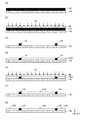
図3は、実施の形態に係る表示パネルの一部を示す模式平面図である。
表示パネル10は、有機化合物の電界発光現象を利用した有機EL表示パネルであり、薄膜トランジスタ(TFT:Thin Film Transistor)が形成された基板100x(TFT基板)に行列状に配された複数の有機EL素子100が、上面より光を発するトップエミッション型の構成を有する。ここで、本明細書では、図3におけるX方向、Y方向、Z方向を、それぞれ表示パネル10における、行方向、列方向、厚み方向とする。FIG. 3 is a schematic plan view showing a part of the display panel according to the embodiment.
The
表示パネル10の表示領域には、複数の有機EL素子100から構成される単位画素100eが行列状に配されている。各単位画素100eには、有機化合物により光を発する領域である、赤色に発光する100aR、緑色に発光する100aG、青色に発光する100aB(以後、100aR、100aG、100aBを区別しない場合は、「100a」と略称する)の3種類の自己発光領域100aが形成されている。すなわち、行方向に並んだ自己発光領域100aR、100aG、100aBのそれぞれに対応する3つの副画素100se(以後、区別する場合は、「青色副画素100seB」、「緑色副画素100seG」及び「赤色副画素100seR」とする)が1組となりカラー表示における単位画素100eを構成している。 In the display area of the
表示パネル10には、複数の補助画素電極150(後述する図4に図示)及び複数の画素電極119が基板100x上に行及び列方向にそれぞれ所定の距離だけ離れた状態で行列状に配されている。複数の補助画素電極150及び画素電極119は、平面視において例えば、概矩形形状であり、画素電極119は光反射材料からなる。行方向に順に3つ並んだ補助画素電極150及び画素電極119は、行方向に順に並んだ3つの自己発光領域100aR、100aG、100aBに対応する。 In the
また、図3及び図4に示すように、表示パネル10には、複数の第1給電補助電極層135(以後、「第1補助電極層135」とする)が基板100x上の単位画素100e間に列方向にわたって連続して配されている。第1補助電極層135は、画素電極119とは異なる光反射材料からなる。また、それぞれの第1補助電極層135の上には、第2給電補助電極層200(以後、「第2補助電極層200」とする)が基板100x上の単位画素100e間に列方向にわたって連続して配されている。第2補助電極層200は、画素電極119と同じ光反射材料からなる。第1補助電極層135の行方向の幅は、後述する製造工程の影響により生じる微差を除外した場合、第2補助電極層200の行方向の幅と同一に構成されている。 3 and 4, the
隣接する画素電極119間には、絶縁層形式のライン状に延伸するバンクが設けられている。また、隣接する画素電極119と第1補助電極層135との間にも、絶縁層形式のライン状に延伸するバンクが設けられている。
画素電極119とこれに隣接する画素電極119とは、互いに絶縁されている。また、画素電極119とこれに隣接する第2補助電極層200又は第1補助電極層135とは、互いに絶縁されている。Between
The
1つの画素電極119と、これに行方向に隣接する画素電極119との間(1つの画素電極119の行方向の外縁119a3と、この画素電極119に行方向に隣接する画素電極119の行方向の外縁119a4との間)、及び、1つの画素電極119と、これに行方向に隣接する第1補助電極層135との間(1つの画素電極119の行方向の外縁119a3と、この画素電極119に行方向に隣接する第1補助電極層135の行方向の外縁135a2との間、及び、1つの画素電極119の行方向の外縁119a4と、この画素電極119に行方向に隣接する第1補助電極層135の行方向の外縁135a1との間)に位置する基板100x上の領域上方には、各条が列方向(図3のY方向)に延伸する列バンク522Yが複数列並設されている。そのため、自己発光領域100aの行方向外縁は、列バンク522Yの行方向外縁により規定される。 Between one
一方、1つの画素電極119と、これに列方向に隣接する画素電極119との間(1つの画素電極119の列方向の外縁119a2と、この画素電極119に列方向に隣接する画素電極119の列方向の外縁119a1との間)に位置する基板100x上の領域上方には、各条が行方向(図3のX方向)に延伸する行バンク122Xが複数行並設されている。行バンク122Xが形成される領域は、画素電極119上方の発光層123において有機電界発光が生じないために非自己発光領域100bとなる。そのため、自己発光領域100aの列方向における外縁は、行バンク122Xの列方向外縁により規定される。 On the other hand, between one
隣り合う列バンク522Y間を間隙522zと定義したとき、間隙522zには、自己発光領域100aRに対応する赤色間隙522zR、自己発光領域100aGに対応する緑色間隙522zG、自己発光領域100aBに対応する青色間隙522zB、第1補助電極層135の配される領域に対応する補助間隙522zA(以後、間隙522zR、間隙522zG、間隙522zB、間隙522zAを区別しない場合は、「間隙522z」と称する)が存在し、表示パネル10は、列バンク522Yと間隙522zとが交互に多数並んだ構成を採る。 When the gap between
表示パネル10では、複数の自己発光領域100aと非自己発光領域100bとが、間隙522zR、間隙522zG、間隙522zBに沿って列方向に交互に並んで配されている。非自己発光領域100bには、画素電極119とTFTのソースS1 とを接続する接続凹部(コンタクトホール、不図示)があり、画素電極119に対して電気接続するための画素電極119上のコンタクト領域(コンタクトウインドウ、不図示)が設けられている。 In the
1つの副画素100seにおいて、列方向に設けられた列バンク522Yと行方向に設けられた行バンク122Xとは直交し、自己発光領域100aは、列方向において行バンク122Xと、この行バンク122Xに隣接する行バンク122Xの間に位置している。
1.4 表示パネル10の各部構成
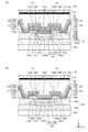
表示パネル10における有機EL素子100の構成を図4及び図5を用いて説明する。図4は、図3におけるA1−A1で切断した模式断面図である。図5は、図4に示す第2補助電極層200周辺の拡大図である。In one subpixel 100se, the
1.4 Configuration of Each Part of
本実施の形態に係る表示パネル10においては、Z軸方向下方に薄膜トランジスタが形成された基板(TFT基板)が構成され、その上に有機EL素子部が構成されている。
1.4.1 基板
(1)基板100x
基板100xは表示パネル10の支持部材であり、基材(不図示)と、基材上に形成された薄膜トランジスタ(TFT:Thin Film Transistor)層(不図示)とを有する。In the
1.4.1 Substrate (1)
The
基材は、表示パネル10の支持部材であり、平板状である。基材の材料としては、電気絶縁性を有する材料、例えば、ガラス材料、樹脂材料、半導体材料、絶縁層をコーティングした金属材料などを用いることができる。
TFT層は、基材上面に形成された複数のTFT及び配線(TFTのソースS1 と、対応する画素電極119を接続する)を含む複数の配線からなる。TFTは、表示パネル10の外部回路からの駆動信号に応じ、自身に対応する画素電極119と外部電源とを電気的に接続するものであり、電極、半導体層、絶縁層などの多層構造からなる。配線は、TFT、画素電極119、外部電源、外部回路などを電気的に接続している。The base material is a support member of the
The TFT layer is composed of a plurality of wirings including a plurality of TFTs and wirings (connecting the TFT source S1 and the corresponding pixel electrode 119) formed on the upper surface of the substrate. The TFT electrically connects the
(2)平坦化層118
基材上及びTFT層の上面には平坦化層118が設けられている。基板100xの上面に位置する平坦化層118は、TFT層によって凹凸が存在する基板100xの上面を平坦化するものである。また、平坦化層118は、配線及びTFTの間を埋め、配線及びTFTの間を電気的に絶縁している。(2)
A
平坦化層118には、画素電極119と対応する画素のソースS1 に接続される配線とを接続するために、画素電極119に対応して、当該配線の上方の一部にコンタクト孔(不図示)が開設されている。
平坦化層118の上限膜厚が10μm以上の場合、製造時の膜厚バラツキがより大きくなると共に、ボトム線幅の制御が困難となる。タクト増大による生産性低下の観点から、平坦化層118の上限膜厚は、7μm以下が望ましい。また、平坦化層118の膜厚とボトム線幅とを同程度にする必要があり、平坦化層118の膜厚が薄くなると、特に、平坦化層118の下限膜厚が1μm以下では、解像度の制約により所望のボトム線幅を得ることが困難となる。一般的なフラットパネルディスプレイ用露光機の場合には平坦化層118の下限膜厚は、2μmが限界となる。したがって、平坦化層118の厚みは、例えば、1μm以上10μm以下、より好ましくは2μm以上7μm以下であることが好ましい。In order to connect the
When the upper limit film thickness of the
1.4.2 有機EL素子部
(1)補助画素電極150及び画素電極119
基板100xの上面に位置する平坦化層118上には、図4及び図5に示すように、副画素100se単位で補助画素電極150が設けられている。さらに、補助画素電極150上には、画素電極119が積層されている。1.4.2 Organic EL element section (1)
On the
補助画素電極150及び画素電極119は、発光層123へキャリアを供給するためのものであり、例えば陽極として機能した場合は、発光層123へホールを供給する。また、表示パネル10がトップエミッション型であるため、画素電極119は光反射性を有する。補助画素電極150及び画素電極119の形状は、例えば、概矩形形状をした平板状である。補助画素電極150及び画素電極119は、行方向に、隣接する第1補助電極層135との間で、間隔δX1をあけて、配されている。また、補助画素電極150及び画素電極119は、行方向に、隣接する補助画素電極150及び画素電極119との間で、間隔δX2をあけて、配されている。平坦化層118のコンタクト孔(不図示)上には、画素電極119の一部を基板100x方向に凹入された画素電極119の接続凹部(コンタクト孔;不図示)が形成されており、接続凹部の底で画素電極119と対応する画素のソースS1 に接続される配線とが接続される。 The
平坦化層118上に、補助画素電極150を形成することにより、密着性が高まり、平坦化層118より下層に水素が入ることを防ぐことができる。TFTに酸化物半導体(TAOS:Transparent Amorphus Oxide Semiconductor)を用いたときに水素によるTFTの劣化を抑制できる。
なお、平坦化層118上には、補助画素電極150を形成しないとしてもよい。By forming the
Note that the
(2)第1補助電極層135及び第2補助電極層200
第1補助電極層135及び第2補助電極層200は、基板100x上方においてそれぞれ補助画素電極150及び画素電極119と同層に延伸し配され、その上に共通電極層125を重畳させて共通電極層125との電気的な接続を図ることにより、共通電極層125の電気抵抗を低減するための補助的な電極層である。基板100xの上面に位置する平坦化層118上には、図4及び図5に示すように、第1補助電極層135が設けられている。第1補助電極層135は、図5に示すように、隣接する画素電極119との間に行方向に間隔δX1をあけて配されている。また、第1補助電極層135は、図5に示すように、隣接するバンク522の基部との間に行方向に間隔をあけて配されている。(2) First
The first
ここで、 第1補助電極層135の厚みは、5nm以上200nm以下であることが好ましく、本実施の形態では、例えば、50nmである。
また、第1補助電極層135上には、図4及び図5に示すように、第2補助電極層200が積層されている。第2補助電極層200の行方向の幅は、第1補助電極層135の行方向の幅と同一である。つまり、第2補助電極層200の上面の面積は、第1補助電極層135の上面の面積と等価である。Here, the thickness of the first
Further, as shown in FIGS. 4 and 5, the second
第2補助電極層200は、アルミニウムを主成分として含み、かつ、少なくとも第2補助電極層200の表層201にはアルミニウムの自然酸化物層が形成されている。アルミニウムの自然酸化物層の厚みは、概ね約3nmから約4nmである。基板作製工程上で大気にさらされることによる大気中での酸素並びに、第2補助電極層200の上方に形成されるホール注入層120Bの成膜後の加熱工程において、ホール注入層120B側から供給される酸素により第2補助電極層200の表層201のアルミニウムが酸化するためである。 The second
(3)ホール注入層120
画素電極119上及び第2補助電極層200上には、図4に示すように、ホール注入層120が積層されている。ホール注入層120は、画素電極119から注入されたホールをホール輸送層121へ輸送する機能を有する。
ホール注入層120は、基板100x側から順に、画素電極119上及び第2補助電極層200上に形成された金属酸化物からなるホール注入層120Aと、後述する間隙522zR、間隙522zG、間隙522zB内のホール注入層120A上それぞれに積層された有機物からなるホール注入層120Bとを含む。青色副画素、緑色副画素及び赤色副画素内に設けられたホール注入層120Aを、それぞれホール注入層120AB、ホール注入層120AG及びホール注入層120AR、第2補助電極層200上に形成されたホール注入層120Aをホール注入層120AAとする。また、青色副画素、緑色副画素及び赤色副画素内に設けられたホール注入層120Bを、それぞれホール注入層120BB、ホール注入層120BG及びホール注入層120BRとする。(3)
On the
The
本実施の形態では、後述する間隙522zR、間隙522zG、間隙522zB内では、ホール注入層120Bは列方向に延伸するように線状に設けられている構成を採る。しかしながら、ホール注入層120Bは、画素電極119上に形成されたホール注入層120A上にのみ形成され、間隙522z内では列方向に断続して設けられている構成としてもよい。 In the present embodiment, the
(4)バンク122
図4、図5に示すように、画素電極119、ホール注入層120、第1補助電極層135及び第2補助電極層200の端縁を被覆するように絶縁物からなるバンクが形成されている。バンクには、列方向に延伸して行方向に複数並設されている列バンク522Yと、行方向に延伸して列方向に複数並設されている行バンク122Xとがある。図3に示すように、列バンク522Yは、行バンク122Xと直交する行方向に沿った状態で設けられており、列バンク522Yと行バンク122Xとで格子状をなしている(以後、行バンク122X、列バンク522Yを区別しない場合は「バンク122」と称する)。(4) Bank 122
As shown in FIGS. 4 and 5, a bank made of an insulating material is formed so as to cover the edges of the
行バンク122Xの形状は、行方向に延伸する線状であり、列方向に平行に切った断面は上方を先細りとする順テーパー台形状である。行バンク122Xは、各列バンク522Yを貫通するようにして、列方向と直交する行方向に沿った状態で設けられており、各々が列バンク522Yの上面522Ybよりも低い位置に上面を有する。そのため、行バンク122Xと列バンク522Yとにより、自己発光領域100aに対応する開口が形成されている。 The shape of the
行バンク122Xは、発光層123の材料となる有機化合物を含んだインクの列方向への流動を制御するためのものである。そのため、行バンク122Xは、インクに対する親液性が所定の値以上であることが必要である。係る構成により、副画素間のインク塗布量の変動を抑制する。行バンク122Xにより画素電極119は、露出することはなく、行バンク122Xが存在する領域では発光せず、輝度には寄与しない。 The
行バンク122Xは、画素電極119の列方向における外縁119a1、a2の上方に存在する。
行バンク122Xは、共通電極層125との間の電気的リークを防止するとともに、列方向における各副画素100seの発光領域100aの外縁を規定する。
列バンク522Yの形状は、列方向に延伸する線状であり、行方向に平行に切った断面は、上方を先細りとする順テーパー台形状である。列バンク522Yは、発光層123の材料となる有機化合物を含んだインクの行方向への流動を堰き止めて形成される発光層123の行方向外縁を規定するものである。The
The
The shape of the
列バンク522Yは、画素電極119の行方向における外縁119a3、a4上方及び第1補助電極層135の行方向における外縁135a1、a2により、行方向の基部が規定されている。列バンク522Yは、共通電極層125との間の電気的リークを防止するとともに、行方向における各副画素100seの発光領域100aの外縁を規定する。列バンク522Yはインクに対する撥液性が所定の値以上であることが必要である。 In the
(5)ホール輸送層121
図4に示すように、間隙522zR、522zG、522zB内におけるホール注入層120上には、ホール輸送層121が積層される。また、行バンク122Xにおけるホール注入層120上にも、ホール輸送層121が積層される(不図示)。ホール輸送層121は、ホール注入層120のホール注入層120Bに接触している。ホール輸送層121は、ホール注入層120から注入されたホールを発光層123へ輸送する機能を有する。間隙522zR、522zG、522zB内に設けられたホール輸送層121を、それぞれホール輸送層121R、ホール輸送層121G及びホール輸送層121Bとする。(5)
As shown in FIG. 4, a
本実施の形態では、後述する間隙522z内では、ホール輸送層121は、ホール注入層120Bと同様、列方向に延伸するように線状に設けられている構成を採る。しかしながら、ホール輸送層121は間隙522z内では列方向に断続して設けられている構成としてもよい。
(6)発光層123
図4に示すように、ホール輸送層121上には、発光層123が積層されている。発光層123は、有機化合物からなる層であり、内部でホールと電子が再結合することで光を発する機能を有する。列バンク522Yにより規定された間隙522zR、間隙522zG、間隙522zB内では、発光層123は、列方向に延伸するように線状に設けられている。赤色副画素100seR内の自己発光領域100aRに対応する赤色間隙522zR、緑色副画素100seG内の自己発光領域100aGに対応する緑色間隙522zG、青色副画素100seB内の自己発光領域100aBに対応する青色間隙522zBには、それぞれ各色に発光する発光層123R、123G、123Bが形成されている。In the present embodiment, in the
(6)
As shown in FIG. 4, the
発光層123は、画素電極119からキャリアが供給される部分のみが発光するので、層間に絶縁物である行バンク122Xが存在する範囲では、有機化合物の電界発光現象が生じない。そのため、発光層123は、行バンク122Xがない部分のみが発光して、この部分が自己発光領域100aとなり、自己発光領域100aの列方向における外縁は、行バンク122Xの列方向外縁により規定される。 Since the
発光層123のうち行バンク122Xの側面及び上面の上方にある部分は発光せず、この部分は非自己発光領域となる。発光層123は、自己発光領域においては、ホール輸送層121の上面に位置し、非自己発光領域100bにおいては行バンク122Xの上面及び側面上のホール輸送層121上面に位置する(不図示)。
なお、発光層123は、自己発光領域100aだけでなく、隣接する非自己発光領域100bまで連続して延伸されている。このようにすると、発光層123の形成時に、自己発光領域100aに塗布されたインクが、非自己発光領域100bに塗布されたインクを通じて列方向に流動でき、列方向の画素間でその膜厚を平準化することができる。但し、非自己発光領域100bでは、行バンク122Xによって、インクの流動が程良く抑制される。よって、列方向に大きな膜厚むらが発生しにくく画素毎の輝度むらが改善される。The portions of the
Note that the
(7)電子輸送層124
図3、図4及び図5に示すように、列バンク522Y及び列バンク522Yにより規定された間隙522zを被覆するように電子輸送層124が積層して形成されている。電子輸送層124については、表示パネル10の少なくとも表示領域全体に連続した状態で形成されている。電子輸送層124は、基板100x側から順に金属酸化物又はフッ化物等からなる電子輸送層124Aと、電子輸送層124A上に積層された有機物を主成分とする電子輸送層124Bとを含む(以後において、電子輸送層124A、124Bを総称する場合は「電子輸送層124」と表記する)。(7)
As shown in FIGS. 3, 4 and 5, the
電子輸送層124は、図4及び図5に示すように、発光層123上に形成されている。電子輸送層124は、共通電極層125からの電子を発光層123へ輸送するとともに、発光層123への電子の注入を制限する機能を有する。
電子輸送層124は、図4及び図5に示すように、第1補助電極層135及び第2補助電極層200の上方にも形成される。したがって、第2補助電極層200上にホール輸送層121が積層されている本実施の形態の構成では、ホール輸送層121上面にも形成される。図5に示すように、電子輸送層124は、第1補助電極層135の端部及び第2補助電極層200の端部において、欠落(段切れ)又は薄層化している。The
As shown in FIGS. 4 and 5, the
ここで、「欠落」とは、電子輸送層124の一部分が途切れて不連続になり下地が見えている状態をさす。欠落によって、電子輸送層3124の欠落している部分において、共通電極層125と第1補助電極層135とが接することにより、両者が電気的に接続される構造を実現することができる。その結果、欠落している部分以外よりも低い電気抵抗にて、共通電極層125と第1補助電極層135とが接続される。 Here, “missing” means a state in which a part of the
また、「薄層化」とは、電子輸送層124の一部分が欠落するには至らないものの、電子輸送層124の一部分が第1補助電極135、第2補助電極200の上平面上よりもその断面部においては薄層化された薄層化部が形成されることをさす。薄層化によって、電子輸送層124の薄層化部において、薄層化部以外の部分よりも低い電気抵抗にて、共通電極層125が第1補助電極層135に電気的に接続される構造を実現することができる。 In addition, “thinning” means that a part of the
また、電子輸送層124においては、金属酸化物又はフッ化物等からなる電子輸送層124Aの抵抗が大きいため、電子輸送層124Aを欠落、薄膜化することだけで大きな効果を得ることができる。
そのため、電子輸送層124が欠落又は薄層化している部分に相当する第2補助電極層200における側面部において、第2補助電極層200の表層201と共通電極層125とが接する構成となる。しかしながら、上述のとおり、第2補助電極層200は、第2補助電極層200の表層201にはアルミニウムの酸化物が形成されているので、第2補助電極層200の表層201と共通電極層125との接触電気抵抗は高いものとなる。Further, in the
Therefore, the
他方、電子輸送層124が欠落又は薄層化している部分に相当する第1補助電極層135における側面上の一部領域135a1、135a2において、第1補助電極層135と共通電極層125の少なくとも一部とが接触している。ここでは、第1補助電極層135の表層部には金属の酸化物が形成されていないので、第1補助電極層135側面上の一部領域135a1、135a2と共通電極層125との接触電気抵抗は低いものとなる。 On the other hand, at least one of the first
このとき、第2補助電極層200と共通電極層125との間には1層以上からなる機能層である電子輸送層124が配されているが、第1補助電極層135の厚みは電子輸送層124の層厚よりも厚いことが好ましい。言い換えると、第1補助電極層135の厚みは、画素電極119(第1補助電極層135)形成後に、第1補助電極層135に積層して真空蒸着法により形成され、電気的接触において高抵抗成分となる機能層の総厚よりも厚いことが好ましい。 At this time, the
係る構成を採ることにより、図5に示すように、第1補助電極層135の側面上の一部領域135a1、135a2において、第1補助電極層135と共通電極層125とを第1補助電極135の上面でより、より低抵抗に接触させることができる。
(8)共通電極層125
図4及び図5に示すように、電子輸送層124上に、共通電極層125が形成されている。共通電極層125は、各発光層123に共通の電極となっている。共通電極層125は、基板100x側から順に金属酸化物からなる共通電極層125Aと、共通電極層125A上に積層された金属を主成分とする共通電極層125Bとを含む(以後において、共通電極層125A、125Bを総称する場合は「共通電極層125」と表記する)。By adopting such a configuration, the first
(8)
As shown in FIGS. 4 and 5, the
共通電極層125は、図4に示すように、電子輸送層124上の画素電極119上方の領域にも形成される。共通電極層125は、画素電極119と対になって発光層123を挟むことで通電経路を作り、発光層123へキャリアを供給するものであり、例えば陰極として機能した場合は、発光層123へ電子を供給する。
共通電極層125Aは、図4及び図5に示すように、第1補助電極層135及び第2補助電極層200上方の領域にも形成される。このとき、共通電極層125Aは、電子輸送層124が欠落又は薄層化している部分に相当する第1補助電極層135の側面上の一部領域135a1、135a2と電気的に接する。As shown in FIG. 4, the
As shown in FIGS. 4 and 5, the
他方、共通電極層125Bは、図4及び図5に示すように、主として共通電極層125Aの上面にのみ形成される。
(9)封止層126
共通電極層125を被覆するように、封止層126が積層形成されている。封止層126は、発光層123が水分や空気などに触れて劣化することを抑制するためのものである。封止層126は、共通電極層125の上面を覆うように設けられている。On the other hand, as shown in FIGS. 4 and 5, the
(9)
A
(10)接合層127
封止層126のZ軸方向上方には、上部基板130のZ軸方向下側の主面にカラーフィルタ層128が形成されたカラーフィルタ基板131が配されており、接合層127により接合されている。接合層127は、基板100xから封止層126までの各層からなる背面パネルとカラーフィルタ基板131とを貼り合わせるとともに、各層が水分や空気に晒されることを防止する機能を有する。(10)
Above the
(11)上部基板130
接合層127の上に、上部基板130にカラーフィルタ層128が形成されたカラーフィルタ基板131が設置・接合されている。上部基板130には、表示パネル10がトップエミッション型であるため、例えば、カバーガラス、透明樹脂フィルムなどの光透過性材料が用いられる。また、上部基板130により、表示パネル10、剛性向上、水分や空気などの侵入防止などを図ることができる。(11)
On the
(12)カラーフィルタ層128
上部基板130には画素の各色自己発光領域100aに対応する位置にカラーフィルタ層128が形成されている。カラーフィルタ層128は、R、G、Bに対応する波長の可視光を透過させるために設けられる透明層であり、各色画素から出射された光を透過させて、その色度を矯正する機能を有する。例えば、本例では、赤色間隙522zR内の自己発光領域100aR、緑色間隙522zG内の自己発光領域100aG、青色間隙522zB内の自己発光領域100aBの上方に、赤色、緑色、青色のフィルタ層128R、128G、128Bが各々形成されている。(12)
A
(13)遮光層129
上部基板130には、各画素の発光領域100a間の境界に対応する位置に遮光層129が形成されている。遮光層129は、R、G、Bに対応する波長の可視光を透過させないために設けられる黒色樹脂層であって、例えば光吸収性及び遮光性に優れる黒色顔料を含む樹脂材料からなる。(13)
A
1.4.3 各部の構成材料
図3、図4及び図5に示す各部の構成材料について、一例を示す。
(1)基板100x(TFT基板)
基材100pとしては、例えば、ガラス基板、石英基板、シリコン基板、硫化モリブデン、銅、亜鉛、アルミニウム、ステンレス、マグネシウム、鉄、ニッケル、金、銀などの金属基板、ガリウム砒素基などの半導体基板、プラスチック基板等を採用することができる。1.4.3 Constituent material of each part An example is shown about the constituent material of each part shown in FIG.3, FIG4 and FIG.5.
(1)
Examples of the
可撓性を有するプラスチック材料として、熱可塑性樹脂、熱硬化性樹脂いずれの樹脂を用いてもよい。可撓性を有する材料からなるフィルムであってもよい。基材の材料としては、電気絶縁性を有する材料、例えば、樹脂材料を用いることができる。具体的には、基板50に用いることが可能な材料としては、例えば、ポリイミド、ポリイミドベンゾオキサゾール、ポリイミドベンゾイミダゾールのほかにポリイミドを単位構造として含む共重合体、ポリエステル、ポリテトラフルオロエチレン、ポリフェニレンスルフィド、ポリアミド、ポリアミドイミド、ポリカーボネート、ポリスチレン、ポリプロピレン、ポリエチレン、ポリ塩化ビニル、ポリエーテルスルホン、ポリエチレンナフタレン、エチレン−プロピレン共重合体、エチレン−酢酸ビニル共重合体等のポリオレフィン、環状ポリオレフィン、変性ポリオレフィン、ポリ塩化ビニル、ポリ塩化ビニリデン、アクリル系樹脂、ポリメチルメタクリレート、アクリル−スチレン共重合体、ブタジエン−スチレン共重合体、エチレン−ビニルアルコール共重合体、ポリエーテル、ポリエーテルケトン、ポリエーテルエーテルケトン、ポリエーテルイミド、ポリアセタール、ポリフェニレンオキシド、変形ポリフェニレンオキシド、ポリアリレート、芳香族ポリエステル、ポリテトラフルオロエチレン、ポリフッ化ビニリデン等が挙げられる。また、これらの材料のうち1種または2種以上を組み合わせた多層構造であってもよい。 As the flexible plastic material, either a thermoplastic resin or a thermosetting resin may be used. A film made of a flexible material may be used. As the material of the base material, a material having electrical insulation, for example, a resin material can be used. Specifically, as a material that can be used for the substrate 50, for example, a copolymer containing polyimide as a unit structure in addition to polyimide, polyimide benzoxazole, polyimide benzimidazole, polyester, polytetrafluoroethylene, polyphenylene sulfide , Polyamide, Polyamideimide, Polycarbonate, Polystyrene, Polypropylene, Polyethylene, Polyvinyl chloride, Polyethersulfone, Polyethylene naphthalene, Ethylene-propylene copolymer, Ethylene-vinyl acetate copolymer, Polyolefin, Cyclic polyolefin, Modified polyolefin, Poly Vinyl chloride, polyvinylidene chloride, acrylic resin, polymethyl methacrylate, acrylic-styrene copolymer, butadiene-styrene copolymer, ethylene Nyl alcohol copolymer, polyether, polyether ketone, polyether ether ketone, polyether imide, polyacetal, polyphenylene oxide, modified polyphenylene oxide, polyarylate, aromatic polyester, polytetrafluoroethylene, polyvinylidene fluoride, etc. . Moreover, the multilayer structure which combined 1 type (s) or 2 or more types among these materials may be sufficient.
TFT層は、基材100pに形成されたTFT回路と、TFT回路上に形成された無機絶縁層116、平坦化層118とを有する。TFT回路は、基材100p上面に形成された複数のTFT及び配線からなる。TFTは、発光素子100の外部回路からの駆動信号に応じ、自身に対応する画素電極119と外部電源とを電気的に接続するものであり、電極、半導体層、絶縁層などの多層構造からなる。配線は、TFT、画素電極12、外部電源、外部回路などを電気的に接続している。 The TFT layer includes a TFT circuit formed on the
TFTを構成するゲート電極、ゲート絶縁層、チャネル層、チャネル保護層、ソース電極、ドレイン電極などには公知の材料を用いることができる。ゲート電極としては、例えば、銅(Cu)とモリブデン(Mo)との積層体を採用している。
ゲート絶縁層103としては、例えば、酸化シリコン(SiO2)、窒化シリコン(SiNx)など、電気絶縁性を有する材料であれば、公知の有機材料や無機材料のいずれも用いることができる。チャネル層としては、インジウム(In)、ガリウム(Ga)、亜鉛(Zn)から選択される少なくとも一種を含む酸化物半導体を採用することができる。Known materials can be used for a gate electrode, a gate insulating layer, a channel layer, a channel protective layer, a source electrode, a drain electrode, and the like constituting the TFT. As the gate electrode, for example, a stacked body of copper (Cu) and molybdenum (Mo) is employed.
As the
チャネル保護層106としては、例えば、酸窒化シリコン(SiON)、窒化シリコン(SiNx)、あるいは酸化アルミニウム(AlOx)を用いることができる。ソース電極、ドレイン電極としては、例えば、銅マンガン(CuMn)と銅(Cu)とモリブデン(Mo)の積層体を採用することができる。
TFT上部の無機絶縁層116は、ガスバリア性を有する無機化合物からなる。例えば、酸化シリコン(SiO2)、窒化シリコン(SiN)や酸窒化シリコン(SiON)、酸化シリコン(SiO)や酸窒化シリコン(SiON)を用いることもできる。As the channel
The inorganic
TFTの接続電極層としては、例えば、モリブデン(Mo)と銅(Cu)と銅マンガン(CuMn)との積層体を採用することができる。なお、接続電極層の構成に用いる材料としては、これに限定されるものではなく、導電性を有する材料から適宜選択することが可能である。
基板100xの上面に位置する平坦化層118の材料としては、例えば、ポリイミド系樹脂、アクリル系樹脂、シロキサン系樹脂、ノボラック型フェノール系樹脂などの有機化合物を用いることができる。As the connection electrode layer of the TFT, for example, a laminate of molybdenum (Mo), copper (Cu), and copper manganese (CuMn) can be employed. Note that the material used for the structure of the connection electrode layer is not limited to this, and can be appropriately selected from conductive materials.
As a material of the
(2)画素電極119、補助画素電極150、第2補助電極層200及び第1補助電極層135
画素電極119は、金属材料から構成されている。トップエミッション型の本実施の形態に係る表示パネル10の場合には、厚みを最適に設定して光共振器構造を採用することにより出射される光の色度を調整し輝度を高めているため、画素電極119の表面部が高い反射性を有することが必要である。本実施の形態に係る表示パネル10では、画素電極119は、金属層、合金層、透明導電膜の中から選択される複数の膜を積層させた構造であってもよい。金属層としては、シート抵抗が小さく、高い光反射性を有する材料として、例えば、銀(Ag)又はアルミニウム(Al)を含む金属材料から構成することができる。例えば、アルミニウム(Al)合金では、反射率が80〜95%と高く、電気抵抗率が、2.82×10⁻⁸(10 nΩm)小さく、第2補助電極層200の材料として好適である。(2)
The
アルミニウム合金などの金属層の他、高反射率の観点から、例えば、銀や銀を含む合金等を用いることができる。透明導電層の構成材料としては、例えば、酸化インジウムスズ(ITO)や酸化インジウム亜鉛(IZO)などを用いることができる。さらに、コスト面からアルミニウムを主成分として含む金属層、合金層を用いることが好ましい。
第2補助電極層200の厚みは、反射率、シート抵抗の観点から数30nm以上500nm以下であることが好ましく、本実施の形態では、例えば、100nmである。In addition to a metal layer such as an aluminum alloy, for example, silver or an alloy containing silver can be used from the viewpoint of high reflectivity. As a constituent material of the transparent conductive layer, for example, indium tin oxide (ITO), indium zinc oxide (IZO), or the like can be used. Furthermore, it is preferable to use a metal layer or an alloy layer containing aluminum as a main component from the viewpoint of cost.
The thickness of the second
なぜなら、第2補助電極層200は、基板上の画素電極119と同時に同層に形成されるために、画素電極119と同じ材料により形成されている。したがって、第2補助電極層200には、アルミニウムを主成分として含む金属層、合金層を用いることが最も好ましい。
第1補助電極層135は、第2補助電極層200を構成する材料と異なる金属を主成分として含み、第2補助電極層200を構成する材料よりも大気中における接触抵抗が低い材料からなる。具体的には、第1補助電極層135は、例えば、タングステン(W)、クロム(Cr)、チタン(Ti)、モリブデン(Mo)、ニッケル(Ni)、銅(Cu)、ランタン(La)、インジウム(In)などの金属材料から形成されることが好ましい。例えば、タングステン(W)は、反射率が50〜60%で、電気抵抗率についても、5.29×10⁻⁸(10 nΩm)程度とアルミニウム(Al)より劣るものの、第2補助電極200の上層には第1の補助電極135が積層され電気的に接触できている。そのため、補助電極としてのシート抵抗は低抵抗化できるととともに、同層で形成される画素電極119としても高い反射も両立できる。このため、下層である第1補助電極層135の材料として好適である。また、同じ思想のもと、第2補助電極としては、ITO又はIZOなどの導電性を有する金属酸化物を用いることができる。第1補助電極層135に、これらの材料を用いることで、第1補助電極だけのシート抵抗としてはアルミニウムには及ばないものの、第2補助電極200との積層により、シート抵抗を低くすることができるとともに、第1補助電極層135の表層部には高抵抗となる金属の酸化物は形成されにくい構成とすることができる。その結果、共通電極層125と接触する第1補助電極層135の側面上の一部領域135a1、135a2と共通電極層125との良好な接触電気抵抗をより低くすることができる。This is because the second
The first
第1補助電極層135の厚みは、上述のとおり、5nm以上200nm以下であることが好ましく、本実施の形態では、例えば、50nmである。
(3)ホール注入層120
ホール注入層120Aは、例えば、銀(Ag)、モリブデン(Mo)、クロム(Cr)、バナジウム(V)、タングステン(W)、ニッケル(Ni)、イリジウム(Ir)などの酸化物からなる層である。ホール注入層120Aを遷移金属の酸化物から構成する場合には、複数の酸化数をとるためこれにより複数の準位をとることができ、その結果、ホール注入が容易になり駆動電圧を低減することができる。As described above, the thickness of the first
(3)
The
本実施の形態では、ホール注入層120Aは、タングステン(W)の酸化物(組成式WOxにおいて、xは概ね2<x<3の範囲における実数)を含む構成とした。このとき、タングステン(W)の酸化物は、5価タングステン原子の6価タングステン原子の比率(W5+/W6+)が大きいほど、有機EL素子の駆動電圧が低くなるため、5価タングステン原子を所定値以上多く含むことが好ましい。ホール注入層120Aは、膜厚が2nm以上(ここでは一例として10nm)30nm以下の酸化タングステン層として構成される。ホール注入層120Aは、酸化タングステンから構成されることが望ましいが、通常混入し得る程度の極微量の不純物が含まれていてもよい。膜厚は2nm以上あると、均一な成膜を行いやすく、また、以下に示す陽極2とホール注入層120との間のショットキーオーミック接続を形成しやすいので、好ましい。ショットキーオーミック接続は酸化タングステンの膜厚が2nm以上で安定して形成されるため、これ以上の膜厚でホール注入層120を形成すれば、ショットキーオーミック接続を利用して、画素電極119からホール注入層120への安定したホール注入効率を期待できる。「ショットキーオーミック接続」とは、画素電極119のフェルミレベルと、前述したホール注入層120のフェルミ面近傍の占有準位で最も低い結合エネルギーとの差が所定値以下に収まっている接続を言う。In this embodiment, the
ホール注入層120Bは、上述のとおり、例えば、PEDOT(ポリチオフェンとポリスチレンスルホン酸との混合物)などの導電性ポリマー材料の有機高分子溶液からなる塗布膜を用いることができる。また、図4に示すように、青色副画素、緑色副画素及び赤色副画素内に設けられたホール注入層120Bを、それぞれホール注入層120BB、120BG及び120BRとしたとき、ホール注入層120BRの厚みは、ホール注入層120BBの厚み及びホール注入層120BGの厚みよりも大きく構成されている。ホール注入層120BBの厚みは0nmより大きく25nm以下であり、ホール注入層120BGの厚みは0nmより大きく30nm以下であり、ホール注入層120BRの厚みは20nm以上50nm以下であることが好ましい。 As described above, for the
(4)バンク122
バンク122は、樹脂等の有機材料を用い形成されており絶縁性を有する。バンク122の形成に用いる有機材料の例としては、アクリル系樹脂、ポリイミド系樹脂、ノボラック型フェノール樹脂等があげられる。バンク122は、有機溶剤耐性を有することが好ましい。より好ましくは、アクリル系樹脂を用いることが望ましい。屈折率が低くリフレクターとして好適であるからである。(4) Bank 122
The bank 122 is formed using an organic material such as a resin and has an insulating property. Examples of the organic material used for forming the bank 122 include acrylic resin, polyimide resin, and novolac type phenol resin. The bank 122 preferably has organic solvent resistance. More preferably, an acrylic resin is used. This is because it has a low refractive index and is suitable as a reflector.
又は、バンク122は、無機材料を用いる場合には、屈折率の観点から、例えば、酸化シリコン(SiO)を用いることが好ましい。あるいは、例えば、窒化シリコン(SiN)、酸窒化シリコン(SiON)などの無機材料を用い形成される。
さらに、バンク122は、製造工程中において、エッチング処理、ベーク処理など施されることがあるので、それらの処理に対して過度に変形、変質などをしないような耐性の高い材料で形成されることが好ましい。Alternatively, when an inorganic material is used for the bank 122, for example, silicon oxide (SiO) is preferably used from the viewpoint of refractive index. Alternatively, for example, an inorganic material such as silicon nitride (SiN) or silicon oxynitride (SiON) is used.
Furthermore, since the bank 122 may be subjected to an etching process, a baking process, or the like during the manufacturing process, the bank 122 is formed of a highly resistant material that does not excessively deform or alter the process. Is preferred.
また、表面に撥水性をもたせるために、表面をフッ素処理することもできる。また、バンク122の形成にフッ素を含有した材料を用いてもよい。また、バンク122の表面に撥水性を低くするために、バンク122に紫外線照射を行う、低温でベーク処理を行ってもよい。
(5)ホール輸送層121
ホール輸送層121は、例えば、ポリフルオレンやその誘導体、あるいはアミン系有機高分子であるポリアリールアミンやその誘導体などの高分子化合物、あるいは、TFB(poly(9、9−di−n−octylfluorene−alt−(1、4−phenylene−((4−sec−butylphenyl)imino)−1、4−phenylene))などを用いることができる。図4に示すように、青色副画素、緑色副画素及び赤色副画素内に設けられたホール輸送層121を、それぞれホール輸送層121B、ホール輸送層121G及びホール輸送層121Rとしたとき、これらの膜厚は概ね10nmから30nmの範囲であることが好ましい。Moreover, in order to give the surface water repellency, the surface can be treated with fluorine. Further, a material containing fluorine may be used for forming the bank 122. Further, in order to reduce the water repellency on the surface of the bank 122, the bank 122 may be baked at a low temperature by irradiating the bank 122 with ultraviolet rays.
(5)
The
(6)発光層123
発光層123は、上述のように、ホールと電子とが注入され再結合されることにより励起状態が生成され発光する機能を有する。発光層123の形成に用いる材料は、湿式印刷法を用い製膜できる発光性の有機材料を用いることが必要である。
具体的には、例えば、特許公開公報(日本国・特開平5−163488号公報)に記載のオキシノイド化合物、ペリレン化合物、クマリン化合物、アザクマリン化合物、オキサゾール化合物、オキサジアゾール化合物、ペリノン化合物、ピロロピロール化合物、ナフタレン化合物、アントラセン化合物、フルオレン化合物、フルオランテン化合物、テトラセン化合物、ピレン化合物、コロネン化合物、キノロン化合物及びアザキノロン化合物、ピラゾリン誘導体及びピラゾロン誘導体、ローダミン化合物、クリセン化合物、フェナントレン化合物、シクロペンタジエン化合物、スチルベン化合物、ジフェニルキノン化合物、スチリル化合物、ブタジエン化合物、ジシアノメチレンピラン化合物、ジシアノメチレンチオピラン化合物、フルオレセイン化合物、ピリリウム化合物、チアピリリウム化合物、セレナピリリウム化合物、テルロピリリウム化合物、芳香族アルダジエン化合物、オリゴフェニレン化合物、チオキサンテン化合物、アンスラセン化合物、シアニン化合物、アクリジン化合物、8−ヒドロキシキノリン化合物の金属錯体、2−ビピリジン化合物の金属錯体、シッフ塩とIII族金属との錯体、オキシン金属錯体、希土類錯体などの蛍光物質で形成されることが好ましい。(6)
As described above, the
Specifically, for example, an oxinoid compound, a perylene compound, a coumarin compound, an azacoumarin compound, an oxazole compound, an oxadiazole compound, a perinone compound, and pyrrolopyrrole described in Japanese Patent Publication (JP-A-5-163488). Compound, naphthalene compound, anthracene compound, fluorene compound, fluoranthene compound, tetracene compound, pyrene compound, coronene compound, quinolone compound and azaquinolone compound, pyrazoline derivative and pyrazolone derivative, rhodamine compound, chrysene compound, phenanthrene compound, cyclopentadiene compound, stilbene compound , Diphenylquinone compound, styryl compound, butadiene compound, dicyanomethylenepyran compound, dicyanomethylenethiopyran compound, fluorene In compounds, pyrylium compounds, thiapyrylium compounds, serenapyrylium compounds, telluropyrylium compounds, aromatic ardadiene compounds, oligophenylene compounds, thioxanthene compounds, anthracene compounds, cyanine compounds, acridine compounds, 8-hydroxyquinoline compound metal complexes, 2- It is preferably formed of a fluorescent substance such as a metal complex of a bipyridine compound, a Schiff salt and a group III metal complex, an oxine metal complex, or a rare earth complex.
(7)電子輸送層124
電子輸送層124には、電子輸送性が高い有機材料が用いられる。電子輸送層124Aは、フッ化ナトリウムで形成された層を含んでいてもよい。電子輸送層124Bに用いられる有機材料としては、例えば、オキサジアゾール誘導体(OXD)、トリアゾール誘導体(TAZ)、フェナンスロリン誘導体(BCP、Bphen)などのπ電子系低分子有機材料が挙げられる。電子輸送層124Aは膜厚が1nm以上10nm以下の範囲で形成されている。(7)
For the
また、電子輸送層124Bは、電子輸送性が高い有機材料に、アルカリ金属、又は、アルカリ土類金属から選択されるドープ金属がドープされて形成された層を含んでいてもよい。アルカリ金属は、具体的には、Li(リチウム)、Na(ナトリウム)、K(カリウム)、Rb(ルビジウム)、Cs(セシウム)、Fr(フランシウム)である。また、アルカリ土類金属は、具体的には、Ca(カルシウム)、Sr(ストロンチウム)、Ba(バリウム)、Ra(ラジウム)である。実施の形態では、Baがドープされている。Baのドープ濃度は40wt%以下であり、20wt%以下が好ましく、15wt%以下がより好ましい。電子輸送層124Bは膜厚が少なくとも10nm以上50nm以下の範囲で形成されている。本実施の形態では、電子輸送層124は、約30nmとした。 The
(8)共通電極層125
共通電極層125Aは、光透過性を有する導電材料が用いられる。例えば、酸化インジウムスズ(ITO)若しくは酸化インジウム亜鉛(IZO)などを用い形成される。
共通電極層125Bは、銀(Ag)又はアルミニウム(Al)などを薄膜化した電極を用い形成される。(8)
For the
The
(9)封止層126
封止層126は、発光層123などの有機層が水分に晒されたり、空気に晒されたりすることを抑制する機能を有し、例えば、窒化シリコン(SiN)、酸窒化シリコン(SiON)などの透光性材料を用い形成される。また、窒化シリコン(SiN)、酸窒化シリコン(SiON)などの材料を用い形成された層の上に、アクリル樹脂、シリコン樹脂などの樹脂材料からなる封止樹脂層を設けてもよい。(9)
The
封止層126は、トップエミッション型である本実施の形態に係る表示パネル10の場合においては、光透過性の材料で形成されることが必要となる。
(10)接合層127
接合層127の材料は、例えば、樹脂接着剤等からなる。接合層127は、アクリル樹脂、シリコン樹脂、エポキシ樹脂などの透光性材料樹脂材料を採用することができる。In the case of the
(10)
The material of the
(11)上部基板130
上部基板130としては、例えば、ガラス基板、石英基板、プラスチック基板等に透光性材料を採用することができる。
(12)カラーフィルタ層128
カラーフィルタ層128としては、公知の樹脂材料(例えば市販製品として、JSR株式会社製カラーレジスト)等を採用することができる。(11)
As the
(12)
As the
(13)遮光層129
遮光層129としては、紫外線硬化樹脂(例えば紫外線硬化アクリル樹脂)材料を主成分とし、これに黒色顔料を添加してなる樹脂材料からなる。黒色顔料としては、例えば、カーボンブラック顔料、チタンブラック顔料、金属酸化顔料、有機顔料など遮光性材料を採用することができる。(13)
The
2 表示パネル10の製造方法
表示パネル10の製造方法について、図6〜11を用いて説明する。図6〜図11における各図は、表示パネル10の製造における各工程での状態を示す図3におけるA1−A1と同じ位置で切断した模式断面図である。
(1)基板100xの準備
複数のTFTや配線が形成された基板100xを準備する。基板100xは、公知のTFTの製造方法により製造することができる(図6(a))。2. Manufacturing method of
(1) Preparation of
(2)平坦化層118の形成
基板100xを被覆するように、上述の平坦化層118の構成材料(感光性の樹脂材料)をフォトレジストとして塗布し、表面を平坦化することにより平坦化層118を形成する(図6(b))。
コンタクト孔(不図示)の形成は、以下のプロセスにより行う。先ず、平坦化層118を形成した後、所定の開口部が施されたフォトマスクを重ね、その上から紫外線照射を行い平坦化層118を露光し、フォトマスクが有するパターンを転写する。その後、現像によって、コンタクト孔をパターニングした平坦化層118を形成する。コンタクト孔の底部において、基板100x上の配線が露出する。ポジ型のフォトレジストを用いて平坦化層118を形成しているが、ネガ型のフォトレジストを用いて平坦化層118を形成してもよい。(2) Formation of the
A contact hole (not shown) is formed by the following process. First, after the
(3)、補助画素電極150、第1補助電極層135、画素電極119、第2補助電極層200、ホール注入層120Aの形成
スパッタリング法、真空蒸着法などの気相成長法を用い金属膜を積層して形成した後、フォトリソグラフィー法及びエッチング法を用いパターニングすることでなされる。
具体的には、先ず、コンタクト孔を開設した平坦化層118を形成した後、平坦化層118の表面にドライエッチング処理を行い製膜前洗浄を行う。(3) Formation of the
Specifically, first, a
次に、補助画素電極150、第1補助電極層135を形成するための第1金属層150Xをスパッタリング法、又は真空蒸着法などの気相成長法により平坦化層118の表面に製膜する(図6(c))。本例では、タングステンをスパッタリング法により製膜する。
さらに、第1金属層150Xの表面に製膜前洗浄を行った後、画素電極119、第2補助電極層200を形成するための第2金属層119Xを気相成長法により第1金属層150Xの表面に製膜する(図6(c))。本例では、アルミニウム又はアルミニウムを主成分とする合金からなる膜をスパッタリング法により製膜する。Next, the first metal layer 150X for forming the
Further, after pre-deposition cleaning is performed on the surface of the first metal layer 150X, the second metal layer 119X for forming the
さらに、第1金属層150Xの表面に製膜前洗浄を行った後、ホール注入層120Aを形成するための第3金属層120AXを気相成長法により第2金属層119Xの表面に製膜する(図6(c))。本例では、タングステンをスパッタリング法により製膜する。
その後、感光性樹脂等からなるフォトレジスト層FRを塗布したのち、所定の開口部が施されたフォトマスクPMを載置し、その上から紫外線照射を行いフォトレジストを露光し、そのフォトレジストにフォトマスクが有するパターンを転写する(図6(d))。次に、フォトレジスト層FRを現像によってパターニングする。Further, after pre-deposition cleaning is performed on the surface of the first metal layer 150X, a third metal layer 120AX for forming the
Then, after applying a photoresist layer FR made of a photosensitive resin or the like, a photomask PM with a predetermined opening is placed, and the photoresist is exposed by irradiating with ultraviolet rays from above, and the photoresist is exposed. A pattern included in the photomask is transferred (FIG. 6D). Next, the photoresist layer FR is patterned by development.
その後、パターニングされたフォトレジスト層FRを介して、第3金属層120AXにドライエッチング処理を施してパターニングを行い、ホール注入層120Aを形成する。
続けて、パターニングされたフォトレジスト層FR及びホール注入層120Aを介して、第2金属層119Xにウエットエッチング処理を施ししてパターニングを行い、画素電極119及び第2補助電極層200を形成する。このとき、ウエットエッチング処理によりパターニングされる第2補助電極層200は、ドライエッチング処理によりパターニンフされる第2金属層119Xがホール注入層120Aや第1補助電極層135よりも、数μm程度オーバエッチングされることがある。本開示においては、第2補助電極層200が第1補助電極層135に重畳して配されていることを要件としているが、重畳して配されているという状態が、第2補助電極層200が第1補助電極層135に対し数μm程度オーバエッチングされていることを許容するものであることは言うまでもない。Thereafter, the third metal layer 120AX is subjected to dry etching through the patterned photoresist layer FR to perform patterning, thereby forming the
Subsequently, the second metal layer 119X is subjected to a wet etching process through the patterned photoresist layer FR and the
さらに、続けて、パターニングされたフォトレジスト層FR及びホール注入層120A、画素電極119及び第2補助電極層200を介して、第1金属層135Xにドライエッチング処理を施してパターニングを行い、補助画素電極150及び第1補助電極層135を形成する。ドライエッチング処理を行う理由は、タングステンや酸化タングステン膜とアルミ系合金とはウェットエッチングレートに大きな差があるため一括に処理することが困難であるため、タングステン、酸化タングステンはアルゴンガス等でのドライエッチングを使用し、アルミ合金はウェットエッチングを本実施の形態では使用したがその限りではない。 Subsequently, the
本実施の形態では、ホール注入層120Aを所定条件で製膜及び焼成することにより、酸素欠陥構造を持つ酸化タングステンを含む酸化タングステン膜からなるホール注入層120を成膜して上述の占有準位を形成する構成としている。
ここでは反応性スパッタ法で成膜することが好適である。成膜ムラの発生が抑制されるからである。具体的には、ターゲットを金属タングステンにして反応性スパッタ法を実施する。スパッタガスとしてアルゴンガス、反応性ガスとして酸素ガスをチャンバー内に導入する。この状態で高電圧によりアルゴンをイオン化し、ターゲットに衝突させる。このとき、スパッタリング現象により放出された金属タングステンが酸素ガスと反応して酸化タングステンとなり成膜される。なお、このときの成膜条件は、いわゆる低レート条件に設定することが好ましい。In this embodiment, the
Here, it is preferable to form the film by a reactive sputtering method. This is because the occurrence of film formation unevenness is suppressed. Specifically, the reactive sputtering method is performed with the target being metallic tungsten. Argon gas as a sputtering gas and oxygen gas as a reactive gas are introduced into the chamber. In this state, argon is ionized by a high voltage and collides with the target. At this time, the metal tungsten released by the sputtering phenomenon reacts with the oxygen gas to form tungsten oxide to form a film. Note that the film formation conditions at this time are preferably set to so-called low rate conditions.
さらに、成膜した酸化タングステン膜に対して個別の焼成工程を実施してもよい。このとき、酸化タングステン膜の成膜を形成する膜厚により複数回に分けて行い、各製膜工程の後に焼成工程を行い、製膜工程と焼成工程とを複数回繰り返す構成としてもよい。これにより、膜密度を高め、溶解耐性を付与する。すなわち、ホール注入層120Aを、酸化タングステン成膜後に所定条件の焼成工程(加熱温度200℃以上230℃以内、加熱時間15分以上45分以内の条件で大気焼成する工程)で焼き締めを図る。これにより、膜密度を、5.8g/cm3以上6.0g/cm3以下の範囲まで増加させる。このように膜密度を増大させることで、製造時のバンク形成工程で用いるエッチング液や洗浄液に対する溶解耐性を付与し膜減りを抑制している。上記焼成条件に基づけば、焼成工程を経ても膜中の酸素欠陥構造は維持されるため、占有準位は温存され、ホール注入特性が低下することはない。このようにして良好なホール注入特性と溶解耐性の両立を高度に両立させる工程を使用したが、タングステン膜を2nm程度の膜厚でスパッタ成膜し、その後、加熱温度200℃以上230℃以内大気焼成する酸化させた酸化タングステン膜の単層またはこれらのタングステン成膜と焼成を複数回実施し、所望の膜厚の酸化タングステン膜のプロセスを適用しても構わない。Further, a separate baking step may be performed on the formed tungsten oxide film. At this time, the tungsten oxide film may be formed in a plurality of times depending on the film thickness to be formed, a baking process may be performed after each film forming process, and the film forming process and the baking process may be repeated a plurality of times. This increases the film density and imparts dissolution resistance. That is, the
最後に、フォトレジスト層FRを剥離して、同一形状にパターニングされた補助画素電極150、画素電極119及びホール注入層120Aの積層体と、第1補助電極層135、第2補助電極層200及びホール注入層120Aの積層体とを形成する(図7(a))。
このとき、コンタクト孔の内壁に沿って金属膜を形成することにより補助画素電極150の接続凹部を形成する。Finally, the photoresist layer FR is peeled off, and a stacked body of the
At this time, a connection concave portion of the
補助画素電極150は、コンタクト孔の底部において露出した基板100x上の配線と接し、TFTの電極と電気的に接続された状態となる。
(4)バンク122の形成
ホール注入層120のホール注入層120Aを形成した後、ホール注入層120Aを覆うようにバンク122を形成する。バンク122の形成では、先ず行バンク122Xを形成し、その後、間隙522Zを形成するように列バンク522Yを形成する(図7(b))。The
(4) Formation of Bank 122 After forming the
バンク122の形成は、先ず、ホール注入層120A上に、スピンコート法などを用い、バンク122の構成材料(例えば、感光性樹脂材料)からなる膜を積層形成する。そして、樹脂膜をパターニングして行バンク122X、列バンク522Yを順に形成する。行バンク122X、列バンク522Yのパターニングは、樹脂膜の上方にフォトマスクを利用し露光を行い、現像工程、焼成工程(約230℃、約60分)をすることによりなされる。 In forming the bank 122, first, a film made of a constituent material of the bank 122 (for example, a photosensitive resin material) is formed on the
具体的には、行バンク122Xの形成工程では、先ず、有機系の感光性樹脂材料、例えば、アクリル系樹脂、ポリイミド系樹脂、ノボラック型フェノール樹脂等からなる感光性樹脂膜を形成した後、乾燥し、溶媒をある程度揮発させてから、所定の開口部が施されたフォトマスクを重ね、その上から紫外線照射を行い感光性樹脂等からなるフォトレジストを露光し、そのフォトレジストにフォトマスクが有するパターンを転写する。次に、感光性樹脂を現像によって行バンク122Xをパターニングした絶縁層を形成する。一般にはポジ型と呼ばれるフォトレジストが使用される。ポジ型は露光された部分が現像によって除去される。露光されないマスクパターンの部分は、現像されずに残存する。 Specifically, in the step of forming the
ここで、ホール注入層120Aは、上述のとおり、スパッタリング法あるいは真空蒸着法などの気相成長法を用い金属(例えば、タングステン)からなる膜を形成した後、フォトリソグラフィー法及びエッチング法を用い各画素単位にパターニングされるが、行バンク122X、列バンク522Yに対する焼成工程において、金属が酸化されホール注入層120Aとして完成する。 Here, as described above, the
列バンク522Yの形成工程では、先ず、スピンコート法などを用い、列バンク522Yの構成材料(例えば、感光性樹脂材料)からなる膜を積層形成する。そして、樹脂膜をパターニングして間隙522zを開設して列バンク522Yを形成する。間隙522zの形成は、樹脂膜の上方にマスクを配して露光し、その後で現像することによりなされる。列バンク522Yは、列方向に延設され、行方向に間隙522zを介して並設される。 In the step of forming the
(5)有機機能層の形成
行バンク122X上を含む列バンク522Yにより規定される間隙522z内に形成されたホール注入層120のホール注入層120A上に対して、ホール注入層120のホール注入層120B、ホール輸送層121、発光層123を順に積層形成する(図7(c))。(5) Formation of organic functional layer Hole injection layer of
ホール注入層120Bは、インクジェット法を用い、PEDOT(ポリチオフェンとポリスチレンスルホン酸との混合物)などの導電性ポリマー材料を含むインクを列バンク522Yにより規定される間隙522z内に塗布した後、溶媒を揮発除去させる。あるいは、焼成することによりなされる。その後、フォトリソグラフィー法およびエッチング法を用い各画素単位にパターニングしてもよい。 The
ホール輸送層121は、インクジェット法やグラビア印刷法によるウェットプロセスを用い、構成材料を含むインクを列バンク522Yにより規定される間隙522z内に塗布した後、溶媒を揮発除去させる、あるいは、焼成することによりなされる(図8(a))。ホール輸送層121のインクを間隙522z内に塗布する方法は、上述したホール注入層120Bにおける方法と同じである。あるいは、スパッタリング法を用い金属(例えば、タングステン)からなる膜を堆積し、焼成によって酸化して形成される。その後、フォトリソグラフィー法及びエッチング法を用い各画素単位にパターニングしてもよい。 The
発光層123の形成は、インクジェット法を用い、構成材料を含むインクを列バンク522Yにより規定される間隙522z内に塗布した後、焼成することによりなされる(図8(a))。具体的には、この工程では、副画素形成領域となる間隙522zに、インクジェット法によりR、G、Bいずれかの有機発光層の材料を含むインク123RI、123GI、123BIをそれぞれ充填し、充填したインクを減圧下で乾燥させ、ベーク処理することによって、発光層123R、123G、123Bを形成する。このとき、発光層123のインクの塗布では、先ず、液滴吐出装置を用いて発光層123の形成するための溶液の塗布を行う。基板100xに対して赤色発光層、緑色発光層、青色発光層の何れかを形成するためのインクの塗布が終わると、次に、その基板に別の色のインクを塗布し、次にその基板に3色目のインクを塗布する工程が繰り返し行われ、3色のインクを順次塗布する。これにより、基板100x上には、赤色発光層、緑色発光層、青色発光層が、図の紙面横方向に繰り返して並んで形成される。発光層123のインクを間隙522z内に塗布する方法の詳細は、上述したホール注入層120Bにおける方法と同じである。 The
ホール注入層120のホール注入層120B、ホール輸送層121、発光層123の形成方法は上記の方法には限定されず、インクジェット法やグラビア印刷法以外の方法、例えばディスペンサー法、ノズルコート法、スピンコート法、凹版印刷、凸版印刷等の公知の方法によりインクを滴下・塗布しても良い。
図3、図4及び図5に示すように、列バンク522Y及び列バンク522Yにより規定された間隙522zを被覆するように電子輸送層124が積層して形成されている。電子輸送層124については、表示パネル10の少なくとも表示領域全体に連続した状態で形成されている。電子輸送層124は、基板100x側から順に金属酸化物又はフッ化物等からなる電子輸送層124Aと、電子輸送層124A上に積層された有機物を主成分とする電子輸送層124Bとを含む(以後において、電子輸送層124A、124Bを総称する場合は「電子輸送層124」と表記する)。The formation method of the
As shown in FIGS. 3, 4 and 5, the
(6)電子輸送層124の形成
発光層123を形成した後、表示パネル10の発光エリア(表示領域)全面にわたって、真空蒸着法などにより電子輸送層124を形成する(図8(b))。真空蒸着法を用いる理由は有機膜である発光層123に損傷を与えないためと、高真空化で行う真空蒸着法は成膜対象の分子が基板に向かって垂直方向に直進的に成膜されるため、本実施の形態における第1補助電極135、第2補助電極200の段面上の一部領域135a1、135a2においては成膜されにくく、欠陥(段切れ)または薄膜化させることができるためである。電子輸送層124は、基板100x側から順に金属酸化物又はフッ化物等からなる電子輸送層124Aと、電子輸送層124A上に積層された有機物を主成分とする電子輸送層124Bからなる。電子輸送層124Aは、発光層123の上に、金属酸化物又はフッ化物を真空蒸着法などにより、例えば、1nm以上10nm以下の膜厚で成膜する。電子輸送層124Aの上に、有機材料と金属材料との共蒸着法により、電子輸送層124Bを、例えば10nm以上、50nm以下の膜厚で成膜する。電子輸送層124は、第2補助電極層200及び第1補助電極層135(第1補助電極層135上において、第2補助電極層200が形成された部分を除く)の上にも形成される。その際、電子輸送層124は、第1補助電極層135の端部及び第2補助電極層200の端部において、欠落(段切れ)又は薄層化して形成される。なお、電子輸送層124A、124Bの膜厚は、一例であり、上記数値に限られるものではなく、光学的な光取り出しとして最も有利となる適切な膜厚とする。(6) Formation of
(7)共通電極層125の形成
電子輸送層124を形成した後、電子輸送層124を被覆するように、共通電極層125を形成する。共通電極層125は、基板100x側から順に金属酸化物からなる共通電極層125Aと、共通電極層125A上に積層された金属を主成分とする共通電極層125Bとを含む。(7) Formation of
このうち、先ず、共通電極層125Aは、電子輸送層124を被覆するように、スパッタリング法などにより形成する(図8(c))。本例では、共通電極層125Aはスパッタリング法を用いてITO又はIZOなどの透明導電層を形成する構成としている。このとき、共通電極層125Aは、第1補助電極層135及び第2補助電極層200上方の領域にも形成され、スパッタリングによる成膜手法は回り込みによって等方的に成膜されやすく、共通電極層125Aは、図4及び図5に示したように、電子輸送層124が欠落又は薄層化している部分に相当する第1補助電極層135の側面上の一部領域135a1、135a2と接する。電子輸送層124は真空蒸着を用いて欠陥(段切れ)や薄膜化させ、共通電極層は被覆性の高いスパッタリング成膜で、回り込み成膜をさせることが重要となる。 Among these, first, the
ここで、共通電極層125の形成方法について、さらに説明する。
まず、図11を用いて、スパッタ装置600の概略構成について説明する。スパッタ装置600は、基板受け渡し室610、成膜室620、ロードロック室630を有し、成膜室620内で、マグネトロンスパッタ法によりスパッタリングを行う。成膜室620には、スパッタリングガスが導入されている。スパッタリングガスには、Ar(アルゴン)等の不活性ガスが用いられる。本実施形態においては、Ar(アルゴン)が用いられる。Here, a method for forming the
First, a schematic configuration of the
スパッタ装置600内のキャリア621には、成膜対象の基板622が設置される。基板622は、基板受け渡し室610において、基板突き上げ機構611によりキャリア621に装着される。基板622が装着されたキャリア621は、基板受け渡し室610から成膜室620を経由してロードロック室630まで、搬送路601上を一定の速度で直線移動する。本実施形態においては、キャリア621の移動速度は30mm/sである。なお、基板622は加温せず、常温でスパッタリングが行われる。 A
成膜室620内には、搬送路601に対して直交する方向に延びる、棒状のターゲット623が設置されている。本実施の形態においては、ターゲット623は、ITO又はIZOである。なお、ターゲット623は、棒状である必要はなく、例えば、粉末状であってもよい。
電源624は、ターゲット623に対して電圧を印加する。なお、図11では電源624は交流電源であるが、直流電源、又は、直流/交流のハイブリッド電源であってもよい。In the
The
排気系631によりスパッタ装置600内を排気し、ガス供給系632により成膜室620内にスパッタリングガスを導入する。電源624によりターゲット623に電圧を印加すると、スパッタリングガスのプラズマが発生し、ターゲット623の表面がスパッタされる。そして、スパッタされたターゲット623の原子を基板622上に堆積させることにより成膜する。 The inside of the
なお、スパッタリングガスであるAr(アルゴン)のガス圧は、例えば、0.6Paであり、流量は100sccmである。
次に、共通電極層125Bは、共通電極層125A上にCVD(Chemical Vapor Deposition)法、スパッタリング法、又は真空蒸着法により形成する(図8(c))。本例では、共通電極層125Bを真空蒸着法により銀を堆積することにより形成する構成としている。共通電極層125Bは、図4及び図5に示すように、主として共通電極層125Aの上面にのみ形成される。ここで、共通電極層125Aを被覆性の高いスパッタ成膜などで、電子輸送層124が欠落又は薄層化している部分に相当する第1補助電極層135の側面上の一部領域135a1、135a2に十分コンタクトできていれば、共通電極総125Bの成膜方法に関しては、真空蒸着法を適用することもできる。In addition, the gas pressure of Ar (argon) which is sputtering gas is 0.6 Pa, for example, and the flow rate is 100 sccm.
Next, the
(8)封止層126の形成
共通電極層125を形成した後、共通電極層125を被覆するように、封止層126を形成する(図8(d))。封止層126は、CVD法、スパッタリング法などを用い形成できる。
(9)カラーフィルタ基板131の形成
次に、カラーフィルタ基板131の製造工程を例示する。(8) Formation of
(9) Formation of the
透明な上部基板130を準備し、紫外線硬化樹脂(例えば紫外線硬化アクリル樹脂)材料を主成分とし、これに黒色顔料を添加してなる遮光層129の材料を透明な上部基板130の一方の面に塗布する(図9(a))。
塗布した遮光層129の上面に所定の開口部が施されたパターンマスクPMを重ね、その上から紫外線照射を行う(図9(b))。A transparent
A pattern mask PM provided with a predetermined opening is overlaid on the upper surface of the coated
その後、パターンマスクPM及び未硬化の遮光層129を除去して現像し、キュアすると、例えば、概矩形状の断面形状の遮光層129が完成する(図9(c))。
次に、遮光層129を形成した上部基板130表面に、紫外線硬化樹脂成分を主成分とするカラーフィルタ層128(例えば、G)の材料128Gを塗布し(図9(d))、所定のパターンマスクPMを載置し、紫外線照射を行う(図9(e))。Thereafter, the pattern mask PM and the uncured
Next, a material 128G of a color filter layer 128 (for example, G) mainly composed of an ultraviolet curable resin component is applied to the surface of the
その後はキュアを行い、パターンマスクPM及び未硬化のペースト128Rを除去して現像すると、カラーフィルタ層128(G)が形成される(図9(f))。
この図9(d)、(e)、(f)の工程を各色のカラーフィルタ材料について同様に繰り返すことで、カラーフィルタ層128(R)、128(B)を形成する(図9(g))。なお、ペースト128Rを用いる代わりに市販されているカラーフィルタ製品を利用してもよい。Thereafter, curing is performed, and when the pattern mask PM and the
Color filter layers 128 (R) and 128 (B) are formed by repeating the steps of FIGS. 9D, 9E, and 9F for each color filter material in the same manner (FIG. 9G). ). A commercially available color filter product may be used instead of using the
以上でカラーフィルタ基板131が形成される。
(10)カラーフィルタ基板131と背面パネルとの貼り合わせ
次に、基板100xから封止層126までの各層からなる背面パネルに、アクリル樹脂、シリコン樹脂、エポキシ樹脂などの紫外線硬化型樹脂を主成分とする接合層127の材料を塗布する(図10(a))。Thus, the
(10) Bonding of
続いて、塗布した材料に紫外線照射を行い、背面パネルとカラーフィルタ基板131との相対的位置関係を合せた状態で両基板を貼り合わせる。このとき、両者の間にガスが入らないように注意する。その後、両基板を焼成して封止工程を完了すると、表示パネル10が完成する(図10(b))。
3.表示パネル10の効果について
以下、表示パネル10から得られる効果について説明する。Subsequently, the applied material is irradiated with ultraviolet rays, and the two substrates are bonded together in a state where the relative positional relationship between the back panel and the
3. Effects of
補助電極層の材料として、金属層としては、シート抵抗が小さく、高い光反射性を有する材料として、銀又はアルミニウムを含む金属材料から構成することができる。このうち、補助電極層を安価なアルミニウムを含む金属材料から構成した場合、補助電極層の表面(表層)に、酸化膜が形成され、補助電極層と共通電極層との接触抵抗が高くなるという課題があった。 As a material of the auxiliary electrode layer, the metal layer can be made of a metal material containing silver or aluminum as a material having low sheet resistance and high light reflectivity. Among these, when the auxiliary electrode layer is made of an inexpensive metal material containing aluminum, an oxide film is formed on the surface (surface layer) of the auxiliary electrode layer, and the contact resistance between the auxiliary electrode layer and the common electrode layer is increased. There was a problem.
係る課題に対し、本実施の形態に係る表示パネル10は、基板100x上に複数の画素電極119が行列状に配され、各画素電極119上に有機発光材料を含む発光層123が配されてなる有機EL表示パネルにおいて、基板100xと、基板100xの上方に行列状に配された複数の画素電極119と、基板100xの上方において、隣接する画素電極119の間隙のうちの少なくとも1の間隙内に列又は行方向に延伸して配された第1補助電極層135と、第1補助電極層135に重畳して配されたアルミニウムを主成分として含み第2補助電極層200と、複数の画素電極119上に配された複数の発光層123と、複数の発光層123の上方と、重畳して配された第1補助電極層135及び第2補助電極層200とを覆って連続して配された共通電極層125とを備える。そして、第1補助電極層135と共通電極層125とは、少なくとも第1補助電極層135の上面に垂直な壁面上の一部領域135a1、a2において接しており、第1補助電極層135は、アルミニウムと異なる金属を主成分として含み、アルミニウムよりも大気中における接触抵抗が低い材料からなることを特徴とする。また、第2給電補助電極層200は、少なくとも第2給電補助電極層200の表層にはアルミニウムの酸化物が形成されている構成であってもよい。 In response to such a problem, in the
ここで、第2補助電極層200は、材料面において、アルミニウムを主成分として含み、かつ、少なくとも第2補助電極層200の表層201にはアルミニウムの自然酸化物が形成されている。その上さらに、少なくとも、第2補助電極層200の上方に形成されるホール注入層120Bの成膜後の加熱工程において、ホール注入層120B側から供給される酸素により第2補助電極層200の表層201のアルミニウムが酸化するためである。 Here, the second
これに対し、第1補助電極層135は、材料面において、第2補助電極層200を構成する材料と異なる金属、例えば、タングステン、クロム、チタン、モリブデン、ニッケル、銅、ランタン、インジウムから選択される1以上の金属を主成分として含む構成である。あるいは、第1補助電極層135はITO又はIZOからなる。このように、第1補助電極層135は、第2補助電極層200を構成する材料よりも大気中における接触抵抗が低い材料からなる。これらの金属又は酸化物は、室温では化学的に安定しているので、第1補助電極層135の表層部には高抵抗となる金属の酸化物が形成されにくい構成としている。そのため、大気中における接触抵抗がアルミニウムよりも低くなる。言い換えれば、第2補助電極層200の表層201付近の抵抗は、第1補助電極層135の表層付近の抵抗より高い構成を実現している。 On the other hand, the first
本実施の形態の構造の効果により、従来断面での段切れによる電気的コンタクトない場合には1000〜2000MΩμm2程度のコンタクト抵抗であったが、本実施の形態では、50〜100MΩμm2程度に1桁以上低抵抗化できることができた。
他方、構造面では、共通電極層125は、重畳して配されている第1補助電極層135及び第2補助電極層200を覆って連続して配されており、第1補助電極層135と共通電極層125とは、少なくとも第1補助電極層135の上面に垂直な壁面上の一部領域135a1、a2において接触している。The effect of the structure of this embodiment has a 1000~2000Emuomegamyuemu2 about the contact resistance in the absence electrical contact by disconnection of the conventional cross-section, in this embodiment, about 50~
On the other hand, in terms of the structure, the
その結果、共通電極層125と接触する第1補助電極層135の側面の一部領域135a1、135a2と共通電極層125との接触電気抵抗をより低くすることができる。すなわち、第1補助電極層135と共通電極層125との間の接触抵抗は、第2補助電極層200と共通電極層125との間の接触抵抗より低くすることができる。
また、従来の構成では、上述のとおり、補助電極層のアルミニウム合金が酸化した場合、補助電極層中に欠陥や異物などの存在により局所的に酸化膜を介さずに補助電極層と共通電極が電気的に接触した場合、その部位に電流が集中し局所的な発熱や材料劣化などが発生することが懸念された。しかしながら、表示パネル10では、共通電極層125と接触する第1補助電極層135の側面の一部領域135a1、135a2と共通電極層125との接触電気抵抗をより低くすることができるので、補助電極層と共通電極とが局所的に酸化膜を介さずに接触しても、その部位における局所的な電流集中や、それに伴う局所的な発熱や材料劣化などを防止できる。As a result, the contact electrical resistance between the
Further, in the conventional configuration, as described above, when the aluminum alloy of the auxiliary electrode layer is oxidized, the auxiliary electrode layer and the common electrode are not locally passed through the oxide film due to the presence of defects or foreign matters in the auxiliary electrode layer. When electrically contacted, there was a concern that current would concentrate on that part and local heat generation or material deterioration would occur. However, in the
以上により、本開示の一態様に係る表示パネル10は、補助電極層に画素電極と同じ光反射性を有する金属材料を用いた構成において、共通電極層と補助電極層との間の電気的接続における接触電気抵抗を低減することができる。その結果、発光効率を向上させると共に輝度ムラを抑制することができる。
また、上記の態様において、さらに、第2補助電極層200と共通電極層125との間には、複数の発光層123の上方、第1補助電極層135及び第2補助電極層200を覆って連続して配された1層以上からなる機能層124を備え、第1補助電極層135の一部領域135a1、135a2付近において、機能層124は欠落又は薄層化しており、第1補助電極層135の厚みは機能層124の厚みよりも厚い構成としてもよい。As described above, in the
Further, in the above aspect, the first
さらに、光学的光取り出しを向上させる目的で電子輸送層の膜厚を、例えば、約100nm程度まで増加する場合においても同様である。第1補助電極層135の厚みを、第2補助電極層200と共通電極層125との間に第1補助電極層135及び第2補助電極層200を覆って連続して配された機能層124の総厚よりも厚い構成とすることにより、共通電極層125を第1補助電極層135の上面に垂直な壁面上の一部領域135a1、a2において確実に接触させることができ、高いキャリア移動度と共通電極層と補助電極層との接触電気抵抗を低減とを両立できることは言うまでもない。 Further, the same applies to the case where the thickness of the electron transport layer is increased to, for example, about 100 nm for the purpose of improving optical light extraction. The thickness of the first
さらに、画素補助電極150と第1補助電極135ならびに、画素電極119と第2補助電極とは同一膜厚とすることで、同一層として同一工程で形成することでプロセスコストを削減することができる。
また、上記の態様において、発光部の光学的設計上、画素電極119とホール注入層120Aとの間に光学調整層として、ITO又はIZOなどを挿入する際、同一層で形成された補助電極部において第2補助電極層200と機能層124との間に、第1補助電極層135及び第2補助電極層200の上方に不連続に配されたITO又はIZOからなる透明導電層を備える構成となっても本開示の効果は発揮される。Further, the pixel
In the above aspect, the auxiliary electrode portion formed of the same layer when ITO or IZO or the like is inserted as an optical adjustment layer between the
また、本実施の形態に係る表示パネル10の製造方法は、基板100x上に複数の画素電極119が行列状に配され、各画素電極119上に有機発光材料を含む発光層123が配されてなる有機EL表示パネルの製造方法であって、基板100xを準備する工程と、基板100xの上方に行列状に複数の画素電極119を形成する工程と、基板100xの上方において、隣接する画素電極119の間隙のうちの少なくとも1の間隙内に列又は行方向に延伸して、アルミニウムと異なる金属を主成分として含み、アルミニウムよりも大気中における接触抵抗が低い材料からなる第1補助電極層135を形成する工程と、第1補助電極層135上に第1補助電極層135と同じ方向に延伸して、第1補助電極層135に重畳して、アルミニウムを主成分として含む第2補助電極層200を形成する工程と、複数の画素電極119上に複数の発光層123を形成する工程と、複数の発光層123の上方、第1補助電極層135及び第2補助電極層200を覆って連続して、かつ、第1補助電極層135と共通電極層125とは、少なくとも第1補助電極層135の上面に垂直な壁面上の一部領域135a1、a2において接するように、共通電極層125をスパッタリング法により形成する工程とを有することを特徴とする。 In the method for manufacturing the
また、上記態様において、第2補助電極層200と共通電極層125との間に、複数の発光層123の上方、第1補助電極層135及び第2補助電極層200を覆って連続して1層以上からなり、第1補助電極層135の厚みよりも薄い機能層124を真空蒸着法により形成する工程を有する構成としてもよい。このとき、機能層124は、第1補助電極層135の一部領域a1、a2付近において欠落又は薄層化して形成される構成としてもよい。 Further, in the above aspect, the first
係る構成により、第1補助電極層135の厚みを、第2補助電極層200とスパッタリング法により形成された共通電極層125との間に蒸着法により連続して配された機能層124の総厚よりも厚い構成とすることにより、スパッタリング法により形成された共通電極層125を蒸着法により形成された機能層124が欠落又は薄層化している第1補助電極層135の上面に垂直な壁面上の一部領域135a1、a2において確実に接触させることができる。 With such a configuration, the thickness of the first
その結果、共通電極層と補助電極層との電気的接続における電気抵抗の低減を図り、発光効率を向上させると共に輝度ムラを抑制することができる表示パネル10を製造できる。
4. 変形例
実施の形態に係る表示パネル10を説明したが、本開示は、その本質的な特徴的構成要素を除き、以上の実施の形態に何ら限定を受けるものではない。例えば、実施の形態に対して当業者が思いつく各種変形を施して得られる形態や、本発明の趣旨を逸脱しない範囲で各実施の形態における構成要素及び機能を任意に組み合わせることで実現される形態も本開示に含まれる。以下では、そのような形態の一例として、表示パネル10の変形例を説明する。As a result, it is possible to manufacture the
4). Although the
(1)変形例1
表示パネル10では、隣接する画素電極119の間隙のうちの少なくとも1の間隙内に列又は行方向に延伸して配された1条の第1補助電極層135と、第1補助電極層135に重畳して配された1条の第2補助電極層200とを備え、第1補助電極層135と共通電極層125とは、少なくとも第1補助電極層135の上面に垂直な側面上の一部領域135a1、a2において接触している構成としている。(1)
In the
しかしながら、第1補助電極層135及び第2補助電極層200の平面形状は上記に限られず適宜変更してもよい。
図12(a)は、変形例1に係る表示パネル10Vに係る表示パネル10Xのバンク及び補助電極層の形状を示す模式平面図である。図13(a)は、図12(a)におけるA3−A3で切断した模式断面図である。変形例1に係る表示パネル10Vは、図12(a)に示すように、隣接するバンク522Vの間隙に列方向に延伸して配された2条の第1補助電極層135V1、V2と、第1補助電極層135に重畳して配された2条の第2補助電極層200V1、V2とを備えた構成としている。図13(a)に示すように、2条の第1補助電極層135V1、V2と2条の第2補助電極層200V1、V2の行方向外側に位置する2本の外縁はそれぞれバンク522Yに覆われている。すなわち、第1補助電極層135は、隣接するバンク522の基部と接触している。また、第2補助電極層200V1、V2には表層201V1、V2に自然酸化物層が形成されている。However, the planar shapes of the first
FIG. 12A is a schematic plan view showing the shapes of banks and auxiliary electrode layers of the
係る構成により、表示パネル10Vでは、表示パネル10に比べて、第1補助電極層135V1及び第2補助電極層200V1の行方向断面に相当する分だけ補助電極の断面積を増加してシート抵抗を低減することができる。併せて、表示パネル10Vでは、第1補助電極層135と共通電極層125とは2条の第1補助電極層135V1の行方向に対向する側面上の一部領域135Va1、Va2において接触している構成を採ることができ、表示パネル10と同様の接触抵抗を実現することができる。 With this configuration, in the
なお、2条の第1補助電極層135V1、V2と、2条の第1補助電極層135を設ける代わりに、1条の第1補助電極層135と1条の第2補助電極層200のそれぞれにスリット状の開口を設けてもよい。
(2)変形例2
変形例3に係る表示パネル10Wでは、第2補助電極層200Wに設けられた貫通孔200Xは、略円形の形状の孔が所定の間隔で列方向に一列に配されている。図12(b)は、変形例2に係る表示パネル10Wに係る表示パネル10Xのバンク及び補助電極層の形状を示す模式平面図である。図13(b)は、図12(b)におけるA4−A4で切断した模式断面図である。変形例2に係る表示パネル10Wは、図12(a)に示すように、隣接するバンク522Wの間隙内に列方向に延伸して配された1条の第1補助電極層135Wと、第1補助電極層135に重畳して配された2条の第2補助電極層200Wとを備え、第2補助電極層200W及び第1補助電極層135を貫通する列方向に並んだ複数の孔200Wa、135Waが開設された構成を採る。図13(b)に示すように、第2補助電極層200W1、W2には表層201W1、W2に自然酸化物層が形成されている。Instead of providing the two first auxiliary electrode layers 135V1 and V2 and the two first auxiliary electrode layers 135, one first
(2)
In the
係る構成により表示パネル10Wでは、第1補助電極層135と共通電極層125とは、第1補助電極層135Wの上面に垂直な側面上の一部領域135a1、a2に加えて、第1補助電極層135に開設された孔135Waの内周面上の一部領域135Wa1、Wa2においても接する構成を採る。このため、表示パネル10と比べて接触面積を増加することができ、表示パネル10に比べて接触抵抗を低減することができる。 With this configuration, in the
(3)変形例3
変形例3に係る表示パネル10Xでは、第2補助電極層200Xに設けられた貫通孔200Xは、略円形の形状の孔が所定の間隔で列方向に二列に配されている。図12(c)は、変形例3に係る表示パネル10Xのバンク及び補助電極層の形状を示す模式平面図である。具体的には、図12(c)に示す変形例3に係る表示パネル10Xのように、隣接するバンク522Yの間隙内に列方向に延伸して配された1条の第1補助電極層135Xと、第1補助電極層135Xに重畳して配された1条の第2補助電極層200Xとを備え、第2補助電極層200X及び第1補助電極層135を貫通する列方向に2列に並んだ複数の孔200Xa、135Xa及び200Xb、135Xbが開設された構成としてもよい。(3) Modification 3
In the
係る構成により、表示パネル10Wに比べてさらに接触面積を増加することができ、より一層接触抵抗を低減することができる。
(4)変形例4
表示パネル10では、第1補助電極層135及び第2補助電極層200は、基板100x上方、平坦化層118の上面においてそれぞれ補助画素電極150及び画素電極119と同層に延伸し配され、その上に共通電極層125を重畳させて共通電極層125との電気的な接続を図る構成としている。With this configuration, the contact area can be further increased as compared with the
(4) Modification 4
In the
しかしながら、基板100x及びその上方において。第1補助電極層135及び第2補助電極層200を設ける層は上記に限られず適宜変更・追加してもよい。
図14(a)は、変形例4に係る表示パネル10Yにおける第2補助電極層200周辺の断面図である。表示パネル10Yでは、表示パネル10Wの構成に加えて、さらに、平坦化層118Yを平坦化下部層118AYと平坦化上部層118BYからなる2層構成とし、平坦化下部層118AYと平坦化上部層118BYとの間に第3給電補助電極層135Yを備えた点に特徴がある。However, on the
FIG. 14A is a cross-sectional view around the second
具体的には、表示パネル10Yは、基板100x上方に樹脂を主成分とする平坦化下部層118AYと平坦化上部層118BYとを備え、平坦化下部層118AYと平坦化上部層118BYとの層間には、列方向に延伸して配された第1補助電極層135Wと同じ材料からなる第3給電補助電極層135Yを備える。このとき、第3給電補助電極層135Yは、行方向において画素電極119と重ならない位置まで拡幅されてもよい。また、第1補助電極層135W上には、第2補助電極層200W、ホール注入層120B、電子輸送層124A、124B、共通電極層125A、125B、封止層126が順に積層されている。さらに、平坦化上部層118BYには、第3給電補助電極層135Yの上面までを貫通するコンタクトホール118BYaが開設されており、第1補助電極層135Wはコンタクトホール118BYa内周面とコンタクトホール118BYaの底面とに連続して配されている。そして、第1補助電極層135Wは、少なくとも第3給電補助電極層135Y上面におけるコンタクトホール118BYa内の一部領域135Yaにおいて第3給電補助電極層135Yと接触している。このとき、上述した変形例3と同様に、共通電極層125との間には機能層124が配されており、第1補助電極層135Wの厚みは機能層124の厚みよりも厚く構成されている。そのため、第1補助電極層135Wは、側面上の一部領域135a1、135a2において共通電極層125Bと接触している。さらに、上述のとおり、第1補助電極層135Wは、コンタクトホール118BYa内において第3給電補助電極層135Yの一部領域135Yaと接触している。これより、第1補助電極層135W上の第2給電補助電極層200Wの表層201Wにアルミニウムの自然酸化物層が形成された場合においても、図14(a)中に示した経路C1、C2により、第1補助電極層135Yを介して共通電極層125と第3給電補助電極層135Yとが電気的に接続される構成とすることができ、第3給電補助電極層135Yを共通電極層125の給電補助電極として機能させることができる。 Specifically, the
その結果、表示パネル10Yでは、表示パネル10Wに比べて、第3給電補助電極層135Yの行方向断面に相当する分だけ補助電極の断面積を増加してシート抵抗を低減することができ、画素密度の増加(高精細化)に伴う光取り出し効率低下抑制のための一手段として有効である。また、基板100x上の平坦化下部層118AYと平坦化上部層118BYとの間の層に補助電極を設ける構成から、TFT配線による位置的制約が少なく、第3給電補助電極層135Yの平面的なレイアウトの自由度が向上する。 As a result, in the
なお、コンタクトホール118BYaを設ける位置は、上記した例に限られず、例えば、コンタクトホール118BYaを図14(a)と異なる位置に設ける構成としてもよい。
さらに、変形例4Aでは、変形例4をさらに変形して、成膜工程において第1補助電極層135W上面をマスキングして第2補助電極層200W、ホール注入層120Bを成膜することにより、第1補助電極層135W上には第2補助電極層200W、ホール注入層120Bを設けない構成としてもよい。図14(b)は、表示パネル10Yにおいて第1補助電極層135W上には第2補助電極層200W及びホール注入層120Bを設けない変形例4Aの断面図である。係る構成では、第1補助電極層135W上に、電子輸送層124A、124B、共通電極層125A、125B、封止層126が順に積層される。電子輸送層124A、124Bは蒸着で形成される場合には、コンタクトホール118BYaの内周面上には形成されない。したがって、コンタクトホール118BYaの深さを共通電極層125A、125Bの層厚よりも大きく採ることにより、コンタクトホール118BYaの内周面上において第1補助電極層135Wの一部領域135a3、135a4が共通電極層125Bとが直接接触する構成とすることができる。あるいは、電子輸送層124A、124Bはスパッタリング法やCVD法で形成される場合には、第1補助電極層135Wは電子輸送層124A、124Bを介して共通電極層125Bと電気的に接続される構成とすることができる。Note that the position where the contact hole 118BYa is provided is not limited to the above example, and for example, the contact hole 118BYa may be provided at a position different from that in FIG.
Further, in the modified example 4A, the modified example 4 is further modified to form the second
係る構成により、共通電極層125と第1給電補助電極層135Wとの接触箇所を増加し、第3給電補助電極層135Yへの給電経路の断面積を増加することができる。その結果、共通電極層125から給電補助電極への接続抵抗を低減できる。
(5)変形例5
表示パネル10Wの構成に加えて、さらに、基板100xを構成する層と層との間に、第4給電補助電極層135Zを備えた構成としてもよい。図15(a)は、変形例5に係る表示パネル10Zにおける第2補助電極層200周辺の断面図である。With such a configuration, the number of contact points between the
(5) Modification 5
In addition to the configuration of the
図15(a)に示すように、表示パネル10Zにおいて、基板100xは、基材100pと、TFT回路を構成するゲート絶縁層103、チャンネル保護層106、それらの上方に無機材料を主成分とする無機絶縁層116とを含む。基板100x上方には、樹脂を主成分とする平坦化層118Yが形成されている。平坦化層118Yは平坦化下部層118AYと平坦化上部層118BYからなる2層構成でもよく、また、単一の層構成であってもよい。 As shown in FIG. 15A, in the display panel 10Z, the
表示パネル10Zでは、基板100xを構成する複数の層の層間において、例えば、チャンネル保護層106と無機絶縁層116との層間には、列又は行方向に延伸して配された第4給電補助電極層135Zを備える。なお、基板100x中の複数の層の層間において、第4給電補助電極層135Zを設ける位置は、チャンネル保護層106と無機絶縁層116との層間には限定されない。また、第4給電補助電極層135Zは、行方向において画素電極119と重ならない位置まで拡幅されてもよい。 In the display panel 10Z, the fourth power supply auxiliary electrode disposed between the plurality of layers constituting the
第1補助電極層135W上には、第2補助電極層200W、ホール注入層120B、電子輸送層124A、124B、共通電極層125A、125B、封止層126が順に積層されている。さらに、平坦化上部層118BY、平坦化下部層118AY、無機絶縁層116には、平坦化上部層118BY上面から第4給電補助電極層135Zの上面までを貫通するコンタクトホール116aが開設されており、第1補助電極層135Wは、コンタクトホール116aに内周面とコンタクトホール116aの底面とに連続して配されている。そして、第4給電補助電極層135Zと第1補助電極層135Wとは、少なくとも第4給電補助電極層135Z上面におけるコンタクトホール116a内の一部領域135Zaにおいて接触している。このとき、上述した変形例3、4と同様に、第1補助電極層135Wは、側面上の一部領域135a1、135a2において共通電極層125Bと接触するとともに、コンタクトホール116a内において第4給電補助電極層135Zの一部領域135Zaとも接触している。 A second
これより、第1補助電極層135W上における第2給電補助電極層200Wの表層201Wにアルミニウムの自然酸化物層が形成された場合でも、図15(a)中に示した経路C3、C4により、第1補助電極層135Wを介して共通電極層125と第4給電補助電極層135Zとが電気的に接続されるので、第4給電補助電極層135Zを共通電極層125の給電補助電極として機能させることができる。 As a result, even when an aluminum natural oxide layer is formed on the
その結果、表示パネル10Zでは、表示パネル10Wに比べて、第4給電補助電極層135Zの行方向断面に相当する分だけ補助電極の断面積を増加してシート抵抗を低減することができ、画素密度の増加(高精細化)に伴う光取り出し効率低下抑制のための一手段として有効である。また、基板100x中のチャンネル保護層106と無機絶縁層116との間に補助電極を設ける構成から、基板100x上の画素電極119等による位置的制約が少なく、第4給電補助電極層135Zの平面的なレイアウトの自由度が向上する。 As a result, in the display panel 10Z, the sheet resistance can be reduced by increasing the cross-sectional area of the auxiliary electrode by an amount corresponding to the cross section in the row direction of the fourth power supply
ここでも、コンタクトホール116aを設ける位置は、上記した例に限られず、例えば、コンタクトホール116aを図15(a)と異なる位置に設ける構成としてもよい。
なお、変形例5Aでは、変形例5をさらに変形して、成膜工程において第1補助電極層135W上面をマスキングして第2補助電極層200W、ホール注入層120Bを成膜することにより、第1補助電極層135W上に第2補助電極層200W、ホール注入層120Bを設けない構成としてもよい。Here, the position where the
In the modified example 5A, the modified example 5 is further modified to form the second
図15(b)は、表示パネル10Zにおいて第1補助電極層135W上に第2補助電極層200W及びホール注入層120Bを設けない変形例5Aの断面図である。係る構成では、第1補助電極層135W上に、電子輸送層124A、124B、共通電極層125A、125B、封止層126が順に積層される。電子輸送層124A、124Bは蒸着で形成される場合には、コンタクトホール116aの内周面上には形成されない。したがって、変形例4と同様に、コンタクトホール116aの内周面上において第1補助電極層135Wの一部領域135a3、135a4が共通電極層125Bとが直接接触するとともに、図15(b)に示す変形例4と比較して、一部領域135a3、135a4の面積を増加することができる。 FIG. 15B is a cross-sectional view of Modification 5A in which the second
係る構成により、共通電極層125と第4給電補助電極層135Zとの接触箇所を増加し、第4給電補助電極層135Zへの給電経路の断面積を増加することができる。その結果、共通電極層125から給電補助電極への接続抵抗を低減できる。
(6)変形例6
変形例4に係る表示パネル10Wの構成と変形例5に係る表示パネル10Zの構成とを組み合わせた構成してもよい。With this configuration, the number of contact points between the
(6) Modification 6
You may comprise the structure which combined the structure of the
図16(a)は、変形例6に係る表示パネル10YZにおける第2補助電極層200周辺の断面図である。表示パネル10YZでは、平坦化下部層118AYと平坦化上部層118BYとの間に第3給電補助電極層135Yを設け、さらに、基板100xを構成する複数の層の層間の何れか、例えば、チャンネル保護層106と無機絶縁層116との層間に第4給電補助電極層135Zを備えた点に特徴がある。ここでも、なお、基板100x中の複数の層の層間において、第4給電補助電極層135Zを設ける位置は、チャンネル保護層106と無機絶縁層116との層間には限定されない。変形例3,4と同様に、第1補助電極層135W上には、第2補助電極層200W、ホール注入層120B、電子輸送層124A、124B、共通電極層125A及び125B、封止層126が順に積層されている。 FIG. 16A is a cross-sectional view around the second
また、平坦化下部層118AY、無機絶縁層116には、平坦化上部層118BY上面から第4給電補助電極層135Zの上面までを貫通するコンタクトホール116aが開設されており、第3補助電極層135Yは、コンタクトホール116aに内周面とコンタクトホール116aの底面とに連続して配されている。そして、第3給電補助電極層135Yと第4給電補助電極層135Zとは、少なくとも第4給電補助電極層135Z上面におけるコンタクトホール116a内の一部領域135Zaにおいて接触している。さらに、平坦化上部層118BYには、第3給電補助電極層135Yの上面までを貫通するコンタクトホール118BYaが開設されており、第1補助電極層135Wは、コンタクトホール118BYaに内周面とコンタクトホール118BYaの底面とに連続して配されている。そして、第1補助電極層135Wは、上述した変形例3、4と同様に、側面上の一部領域135a1、135a2において共通電極層125Bと接触するとともに、第1補助電極層135Wと第3給電補助電極層135Yとは、少なくとも第3給電補助電極層135Y上面におけるコンタクトホール118BYa内の一部領域135Yaにおいて接触している。 Further, in the planarization lower layer 118AY and the inorganic insulating
これより、第1補助電極層135W上における第2給電補助電極層200Wの表層201Wにアルミニウムの自然酸化物層が形成された場合でも、図16(a)中に示した経路C5、C6により、第1補助電極層135Wを介して共通電極層125と第3給電補助電極層135Y、さらに第4給電補助電極層135Zが電気的に接続されるので、第3給電補助電極層135Y及び135Zを共通電極層125の給電補助電極として機能させることができる。そのため、より一層シート抵抗を低減することができ高精細化に向けて有効である。また、チャンネル保護層106と絶縁層116との間の層において、TFT回路の配線による位置的制約がない範囲において、第4給電補助電極層135Zの平面的に自由にレイアウトできる。 As a result, even when an aluminum natural oxide layer is formed on the
なお、変形例6Aでは、変形例6をさらに変形して、第1補助電極層135W上に第2補助電極層200W、ホール注入層120Bを設けない構成としてもよい。
図16(b)は、表示パネル10YZにおいて第1補助電極層135W上に第2補助電極層200W及びホール注入層120Bを設けない変形例6Aの断面図である。係る構成では、第1補助電極層135W上に、電子輸送層124A、124B、共通電極層125A、125B、封止層126が順に積層される。電子輸送層124A、124Bは蒸着で形成される場合には、コンタクトホール116aの内周面上には形成されない。したがって、変形例4、5と同様に、コンタクトホール116aの内周面上において第1補助電極層135Wの一部領域135a3、135a4が共通電極層125Bとが直接接触するとともに、図16(b)に示す変形例4と比較して、一部領域135a3、135a4の面積を増加することができる。In Modification 6A, Modification 6 may be further modified such that the second
FIG. 16B is a cross-sectional view of Modification 6A in which the second
係る構成により、共通電極層125と第1給電補助電極層135Wとの接触箇所を増加し、第3給電補助電極層135Y及び第4給電補助電極層135Zへの給電経路の断面積を増加することができ、共通電極層125から給電補助電極への接続抵抗を低減できる。
(7)その他の変形例
表示パネル10では、発光層123は、行バンク上を列方向に連続して延伸している構成としている。しかしながら、上記構成において、発光層123は、行バンク上において画素ごとに断続している構成としてもよい。With this configuration, the number of contact points between the
(7) Other Modifications In the
また、表示パネル10では、行方向に隣接する列バンク522Y間の間隙522zに配された副画素100seの発光層123が発する光の色は互いに異なる構成とし、列方向に隣接する行バンク122X間の間隙に配された副画素100seの発光層123が発する光の色は同じである構成とした。しかしながら、上記構成において、行方向に隣接する副画素100seの発光層123が発する光の色は同じであり、列方向に隣接する副画素100seの発光層123が発する光の色が互いに異なる構成としてもよい。また、行列方向の両方において隣接する副画素100seの発光層123が発する光の色が互いに異なる構成としてもよい。 In the
実施の形態に係る表示パネル10では、画素100eには、赤色画素、緑色画素、青色画素の3種類があったが、本発明はこれに限られない。例えば、発光層が1種類であってもよいし、発光層が赤、緑、青、白色などに発光する4種類であってもよい。
また、上記実施の形態では、単位画素100eが、マトリクス状に並んだ構成であったが、本発明はこれに限られない。例えば、画素領域の間隔を1ピッチとするとき、隣り合う間隙同士で画素領域が列方向に半ピッチずれている構成に対しても効果を有する。高精細化が進む表示パネルにおいて、多少の列方向のずれは視認上判別が難しく、ある程度の幅を持った直線上(あるいは千鳥状)に膜厚むらが並んでも、視認上は帯状となる。したがって、このような場合も輝度むらが上記千鳥状に並ぶことを抑制することで、表示パネルの表示品質を向上できる。In the
In the above embodiment, the
また、上記実施の形態では、画素電極119と共通電極層125の間に、ホール注入層120、ホール輸送層121、発光層123及び電子輸送層124が存在する構成であったが、本発明はこれに限られない。例えば、ホール注入層120、ホール輸送層121及び電子輸送層124を用いずに、画素電極119と共通電極層125との間に発光層123のみが存在する構成としてもよい。また、例えば、ホール注入層、ホール輸送層、電子輸送層、電子注入層などを備える構成や、これらの複数又は全部を同時に備える構成であってもよい。また、これらの層はすべて有機化合物からなる必要はなく、無機物などで構成されていてもよい。 In the above embodiment, the
また、上記実施の形態では、発光層123の形成方法としては、印刷法、スピンコート法、インクジェット法などの湿式成膜プロセスを用いる構成であったが、本発明はこれに限られない。例えば、真空蒸着法、電子ビーム蒸着法、スパッタリング法、反応性スパッタリング法、イオンプレーティング法、気相成長法等の乾式成膜プロセスを用いることもできる。さらに、各構成部位の材料には、公知の材料を適宜採用することができる。 In the above embodiment, the
また、上記の形態では、EL素子部の下部にアノードである画素電極3119が配され、TFTのソース電極に接続された配線110に画素電極3119を接続する構成を採用したが、EL素子部の下部に共通電極層、上部にアノードが配された構成を採用することもできる。この場合には、TFTにおけるドレインに対して、下部に配されたカソードを接続することになる。 Further, in the above embodiment, the pixel electrode 3119 which is an anode is arranged below the EL element portion, and the pixel electrode 3119 is connected to the wiring 110 connected to the source electrode of the TFT. A configuration in which a common electrode layer is disposed in the lower portion and an anode is disposed in the upper portion may be employed. In this case, the cathode arranged at the lower side is connected to the drain of the TFT.
また、上記実施の形態では、一つの副画素100seに対して2つのトランジスタTr1、Tr2が設けられてなる構成を採用したが、本発明はこれに限定を受けるものではない。例えば、一つのサブピクセルに対して一つのトランジスタを備える構成でもよいし、三つ以上のトランジスタを備える構成でもよい。
さらに、上記実施の形態では、トップエミッション型のEL表示パネルを一例としたが、本発明はこれに限定を受けるものではない。例えば、ボトムエミッション型の表示パネルなどに適用することもできる。その場合には、各構成について、適宜の変更が可能である。In the above embodiment, a configuration in which two transistors Tr1 and Tr2 are provided for one sub-pixel 100se is employed. However, the present invention is not limited to this. For example, one transistor may be provided with one transistor, or three or more transistors may be provided.
Furthermore, in the above embodiment, the top emission type EL display panel is taken as an example, but the present invention is not limited to this. For example, the present invention can be applied to a bottom emission type display panel. In that case, it is possible to appropriately change each configuration.
≪補足≫
以上で説明した実施の形態は、いずれも本発明の好ましい一具体例を示すものである。実施の形態で示される数値、形状、材料、構成要素、構成要素の配置位置及び接続形態、工程、工程の順序などは一例であり、本発明を限定する主旨ではない。また、実施の形態における構成要素のうち、本発明の最上位概念を示す独立請求項に記載されていない工程については、より好ましい形態を構成する任意の構成要素として説明される。<Supplement>
Each of the embodiments described above shows a preferred specific example of the present invention. The numerical values, shapes, materials, constituent elements, arrangement positions and connection forms of the constituent elements, steps, order of steps, and the like shown in the embodiments are merely examples, and are not intended to limit the present invention. In addition, among the constituent elements in the embodiment, steps that are not described in the independent claims indicating the highest concept of the present invention are described as arbitrary constituent elements constituting a more preferable form.
また、上記の工程が実行される順序は、本発明を具体的に説明するために例示するためのものであり、上記以外の順序であってもよい。また、上記工程の一部が、他の工程と同時(並列)に実行されてもよい。
また、発明の理解の容易のため、上記各実施の形態で挙げた各図の構成要素の縮尺は実際のものと異なる場合がある。また本発明は上記各実施の形態の記載によって限定されるものではなく、本発明の要旨を逸脱しない範囲において適宜変更可能である。In addition, the order in which the above steps are performed is for illustration in order to specifically describe the present invention, and may be in an order other than the above. Moreover, a part of said process may be performed simultaneously with another process (parallel).
Further, for easy understanding of the invention, the scales of the components shown in the above-described embodiments may be different from actual ones. The present invention is not limited by the description of each of the above embodiments, and can be appropriately changed without departing from the gist of the present invention.
また、各実施の形態及びその変形例の機能のうち少なくとも一部を組み合わせてもよい。
さらに、本実施の形態に対して当業者が思いつく範囲内の変更を施した各種変形例も本発明に含まれる。Moreover, you may combine at least one part among the functions of each embodiment and its modification.
Furthermore, various modifications in which the present embodiment is modified within the range conceivable by those skilled in the art are also included in the present invention.
本発明に係る有機EL表示パネル、及び有機EL表示装置は、テレビジョンセット、パーソナルコンピュータ、携帯電話などの装置、又はその他表示パネルを有する様々な電子機器に広く利用することができる。 The organic EL display panel and the organic EL display device according to the present invention can be widely used in various electronic devices having devices such as a television set, a personal computer, a mobile phone, and other display panels.
1 有機EL表示装置
10、10V、10W、10X、10Y、10Z 有機EL表示パネル
100 有機EL素子
100e 単位画素
100se 副画素
100a 自己発光領域
100b 非自己発光領域
100x 基板(TFT基板)
100p 基台
103 ゲート絶縁層
106 チャンネル保護層
116 無機絶縁層
118 層間絶縁層
119 画素電極
135、135W 第1補助電極層
135Y 第3補助電極層
135Z 第4補助電極層
150 補助画素電極
200 第2補助電極層
120、120A、120B ホール注入層
121 ホール輸送層
122 バンク
122X 行バンク
522Y 列バンク
123 発光層
124、124A、124B 電子輸送層
125、125A、125B 共通電極層
126 封止層
127 接合層
128 カラーフィルタ層
130 上部基板
131 カラーフィルタ基板DESCRIPTION OF
Claims (21)
Translated fromJapanese基板と、
前記基板の上方に行列状に配された複数の画素電極と、
前記基板の上方において、隣接する前記画素電極の間隙のうちの少なくとも1の間隙内に列又は行方向に延伸して配された第1給電補助電極層と、
前記第1給電補助電極層に重畳して配されたアルミニウムを主成分として含む第2給電補助電極層と、
前記複数の画素電極上に配された複数の発光層と、
前記複数の発光層の上方、前記第1給電補助電極層及び前記第2給電補助電極層を覆って連続して配された共通電極層とを備え、
前記第1給電補助電極層と前記共通電極層とは、少なくとも前記第1給電補助電極層の上面に垂直な壁面上の一部領域において接触しており、
前記第1給電補助電極層は、アルミニウムと異なる金属を主成分として含み、アルミニウムよりも大気中における接触抵抗が低い材料からなる
有機EL表示パネル。An organic EL display panel in which a plurality of pixel electrodes are arranged in a matrix on a substrate, and a light emitting layer containing an organic light emitting material is arranged on each pixel electrode,
A substrate,
A plurality of pixel electrodes arranged in a matrix above the substrate;
A first power supply auxiliary electrode layer disposed above the substrate and extending in the column or row direction in at least one of the gaps between the adjacent pixel electrodes;
A second power supply auxiliary electrode layer containing as a main component aluminum disposed so as to overlap the first power supply auxiliary electrode layer;
A plurality of light emitting layers disposed on the plurality of pixel electrodes;
A common electrode layer disposed above the plurality of light emitting layers, continuously covering the first power supply auxiliary electrode layer and the second power supply auxiliary electrode layer,
The first power supply auxiliary electrode layer and the common electrode layer are in contact with each other at least in a partial region on the wall surface perpendicular to the upper surface of the first power supply auxiliary electrode layer,
The first power supply auxiliary electrode layer is an organic EL display panel made of a material containing a metal different from aluminum as a main component and having a lower contact resistance in the atmosphere than aluminum.
請求項1に記載の有機EL表示パネル。The organic EL display panel according to claim 1, wherein the second power supply auxiliary electrode layer has an aluminum oxide formed on at least a surface layer of the second power supply auxiliary electrode layer.
前記第1給電補助電極層の一部領域付近において、前記機能層は欠落又は薄層化しており、
前記第1給電補助電極層の厚みは前記発光層上の前記機能層の厚みよりも厚い
請求項1又は2に記載の有機EL表示パネル。Further, the second power supply auxiliary electrode layer and the common electrode layer are continuously arranged above the light emitting layers, covering the first power supply auxiliary electrode layer and the second power supply auxiliary electrode layer. A functional layer composed of one or more layers,
In the vicinity of a partial region of the first power supply auxiliary electrode layer, the functional layer is missing or thinned,
The organic EL display panel according to claim 1, wherein a thickness of the first power feeding auxiliary electrode layer is thicker than a thickness of the functional layer on the light emitting layer.
請求項1から3の何れか1項に記載の有機EL表示パネル。4. The organic EL display panel according to claim 1, wherein a resistance near a surface layer of the second power feeding auxiliary electrode layer is higher than a resistance near a surface layer of the first power feeding auxiliary electrode layer. 5.
請求項1から4の何れか1項に記載の有機EL表示パネル。The contact resistance between the first power supply auxiliary electrode layer and the common electrode layer is lower than the contact resistance between the second power supply auxiliary electrode layer and the common electrode layer. An organic EL display panel described in 1.
請求項1から4の何れか1項に記載の有機EL表示パネル。The organic EL display panel according to any one of claims 1 to 4, wherein the sheet resistance of the material is higher than that of aluminum.
請求項1から6の何れか1項に記載の有機EL表示パネル。The organic EL display panel according to any one of claims 1 to 6, wherein the metal different from aluminum is at least one metal selected from tungsten, chromium, titanium, molybdenum, nickel, copper, lanthanum, and indium.
請求項1から6の何れか1項に記載の有機EL表示パネル。The organic EL display panel according to claim 1, wherein the first power supply auxiliary electrode layer is made of ITO or IZO.
さらに、前記第2給電補助電極層と前記第1の機能層との間には、前記複数の発光層の下方、前記第1給電補助電極層及び前記第2給電補助電極層の上方に不連続に配された第2の機能層を備える
請求項3の何れか1項に記載の有機EL表示パネル。When the functional layer is a first functional layer,
Further, there is a discontinuity between the second power supply auxiliary electrode layer and the first functional layer below the plurality of light emitting layers and above the first power supply auxiliary electrode layer and the second power supply auxiliary electrode layer. The organic EL display panel according to claim 3, further comprising a second functional layer disposed on the organic EL display panel.
請求項3の何れか1項に記載の有機EL表示パネル。Furthermore, the second power supply auxiliary electrode layer and the functional layer are discontinuously disposed below the plurality of light emitting layers and above the first power supply auxiliary electrode layer and the second power supply auxiliary electrode layer. The organic electroluminescence display panel according to claim 3, further comprising a transparent conductive layer made of ITO or IZO.
請求項1から10の何れか1項に記載の有機EL表示パネル。The organic EL display panel according to claim 1, wherein the common electrode layer includes a transparent conductive layer made of ITO or IZO.
請求項1から11の何れか1項に記載の有機EL表示パネル。The organic EL display panel according to claim 1, wherein the common electrode layer includes a metal electrode layer containing silver as a main component.
前記平坦化下部層と前記平坦化上部層とのとの間には、列又は行方向に延伸して配された、第3給電補助電極層とを備え、
前記平坦化上部層には前記第3給電補助電極層の上面までを貫通するコンタクトホールが開設されており、前記第1給電補助電極層が前記第3補助電極層と前記コンタクトホールを介して電気的に接続されており、
前記共通電極層は、前記コンタクトホールに内周面と底面とに連続して配されており、
前記第3給電補助電極層と前記共通電極層とは、前記第1給電補助電極層を介して電気的に接続されている
請求項1から12の何れか1項に記載の有機EL表示パネル。A flattening layer comprising a flat lower layer mainly composed of a resin and a flattening upper layer above the substrate,
Between the flattening lower layer and the flattening upper layer, a third power supply auxiliary electrode layer arranged to extend in a column or row direction,
A contact hole penetrating up to the upper surface of the third power supply auxiliary electrode layer is formed in the flattening upper layer, and the first power supply auxiliary electrode layer is electrically connected to the third auxiliary electrode layer and the contact hole. Connected,
The common electrode layer is continuously arranged in the contact hole on the inner peripheral surface and the bottom surface,
The organic EL display panel according to any one of claims 1 to 12, wherein the third power supply auxiliary electrode layer and the common electrode layer are electrically connected via the first power supply auxiliary electrode layer.
前記コンタクトホールの深さは前記機能層の厚みよりも厚く、前記第1給電補助電極層と前記共通電極層とは、少なくとも前記第1給電補助電極層における前記コンタクトホールに内周面上の一部領域において接触している
請求項13に記載の有機EL表示パネル。Furthermore, a functional layer is disposed between the bottom surface of the contact hole and the common electrode layer in the contact hole,
The depth of the contact hole is greater than the thickness of the functional layer, and the first power supply auxiliary electrode layer and the common electrode layer are at least one on the inner peripheral surface of the contact hole in the first power supply auxiliary electrode layer. The organic EL display panel according to claim 13, which is in contact in a partial area.
前記基板上方に樹脂を主成分とする平坦化層を備え、
前記TFT基板と前記絶縁層との間には、列又は行方向に延伸して配された第4給電補助電極層を備え、
前記平坦化層には、当該平坦化層上面から前記第4給電補助電極層の下面までを貫通するコンタクトホールが開設されており、前記第1給電補助電極層が前記第4補助電極層と前記コンタクトホールを介して電気的に接続されており、
前記共通電極層は、前記コンタクトホールに内周面と底面とに連続して配されており、 前記第4給電補助電極層と前記共通電極層とは、前記第1給電補助電極層を介して電気的に接続されている
請求項1から12の何れか1項に記載の有機EL表示パネル。The substrate includes a TFT substrate and an insulating layer mainly composed of a resin above the TFT substrate,
A planarizing layer mainly composed of a resin is provided above the substrate,
Between the TFT substrate and the insulating layer is provided with a fourth power supply auxiliary electrode layer arranged extending in the column or row direction,
The planarization layer has a contact hole penetrating from the upper surface of the planarization layer to the lower surface of the fourth power supply auxiliary electrode layer, and the first power supply auxiliary electrode layer is connected to the fourth auxiliary electrode layer and the fourth power supply electrode layer. Are electrically connected through contact holes,
The common electrode layer is continuously disposed in the contact hole on an inner peripheral surface and a bottom surface, and the fourth power supply auxiliary electrode layer and the common electrode layer are interposed via the first power supply auxiliary electrode layer. The organic EL display panel according to claim 1, wherein the organic EL display panel is electrically connected.
前記コンタクトホールの深さは前記機能層の厚みよりも厚く、前記第1給電補助電極層と前記共通電極層とは、少なくとも前記第1給電補助電極層における前記コンタクトホールに内周面上の一部領域において接触している
請求項15に記載の有機EL表示パネル。Furthermore, a functional layer is disposed between the bottom surface of the contact hole in the substrate and the common electrode layer in the contact hole,
The depth of the contact hole is greater than the thickness of the functional layer, and the first power supply auxiliary electrode layer and the common electrode layer are at least one on the inner peripheral surface of the contact hole in the first power supply auxiliary electrode layer. The organic EL display panel according to claim 15, which is in contact in a partial area.
前記基板上方に樹脂を主成分とする平坦下部層と平坦化上部層からなる平坦化層を備え、
前記平坦化下部層と前記平坦化上部層との間には、列又は行方向に延伸して配された、第3給電補助電極層を備え、
前記TFT基板と前記絶縁層との間には、列又は行方向に延伸して配された第4給電補助電極層を備え、
前記平坦化下部層、前記平坦化上部層、及び前記絶縁層には前記第4給電補助電極層の上面までを貫通するコンタクトホールが開設されており、
前記第1給電補助電極層は前記第3補助電極層と前記コンタクトホールを介して電気的に接続されており、
前記第3給電補助電極層は前記第4補助電極層と前記コンタクトホールを介して電気的に接続されており、
前記共通電極層は、前記コンタクトホールに内周面と底面とに連続して配されており、
前記第3給電補助電極層及び前記第4補助電極層と、前記共通電極層とは、前記第1給電補助電極層を介して電気的に接続されている
請求項1から12の何れか1項に記載の有機EL表示パネル。The substrate includes a TFT substrate and an insulating layer mainly composed of a resin above the TFT substrate,
A flattening layer comprising a flat lower layer mainly composed of a resin and a flattening upper layer above the substrate,
Between the flattening lower layer and the flattening upper layer, a third power supply auxiliary electrode layer disposed extending in the column or row direction is provided,
Between the TFT substrate and the insulating layer is provided with a fourth power supply auxiliary electrode layer arranged extending in the column or row direction,
A contact hole is formed in the planarization lower layer, the planarization upper layer, and the insulating layer so as to penetrate to the upper surface of the fourth power supply auxiliary electrode layer.
The first power supply auxiliary electrode layer is electrically connected to the third auxiliary electrode layer through the contact hole,
The third power supply auxiliary electrode layer is electrically connected to the fourth auxiliary electrode layer via the contact hole;
The common electrode layer is continuously arranged in the contact hole on the inner peripheral surface and the bottom surface,
The third power supply auxiliary electrode layer, the fourth auxiliary electrode layer, and the common electrode layer are electrically connected via the first power supply auxiliary electrode layer. An organic EL display panel described in 1.
前記コンタクトホールの深さは前記機能層の厚みよりも厚く、前記第1給電補助電極層と前記共通電極層とは、少なくとも前記第1給電補助電極層における前記コンタクトホールに内周面上の一部領域において接触している
請求項17に記載の有機EL表示パネル。Furthermore, a functional layer is disposed between the bottom surface of the contact hole and the common electrode layer in the contact hole,
The depth of the contact hole is greater than the thickness of the functional layer, and the first power supply auxiliary electrode layer and the common electrode layer are at least one on the inner peripheral surface of the contact hole in the first power supply auxiliary electrode layer. The organic EL display panel according to claim 17, wherein the organic EL display panel is in contact in a partial area.
基板を準備する工程と、
前記基板の上方に行列状に複数の画素電極を形成する工程と、
前記基板の上方において、隣接する前記画素電極の間隙のうちの少なくとも1の間隙内に列又は行方向に延伸して、アルミニウムと異なる金属を主成分として含み、アルミニウムよりも大気中における接触抵抗が低い材料からなる第1給電補助電極層を形成する工程と、
前記第1給電補助電極層上に前記第1給電補助電極層と同じ方向に延伸して、前記第1給電補助電極層に重畳して、アルミニウムを主成分として含む第2給電補助電極層を形成する工程と、
前記複数の画素電極上に複数の発光層を形成する工程と、
前記複数の発光層の上方、前記第1給電補助電極層及び前記第2給電補助電極層を覆って連続して、かつ、前記第1給電補助電極層と前記共通電極層とは、少なくとも前記第1給電補助電極層の上面に垂直な壁面上の一部領域において接するように、共通電極層をスパッタリング法により形成する工程とを有する
有機EL表示パネルの製造方法。A method of manufacturing an organic EL display panel in which a plurality of pixel electrodes are arranged in a matrix on a substrate, and a light emitting layer containing an organic light emitting material is arranged on each pixel electrode,
Preparing a substrate;
Forming a plurality of pixel electrodes in a matrix above the substrate;
Above the substrate, it extends in the column or row direction in at least one of the gaps between the adjacent pixel electrodes, and contains a metal different from aluminum as a main component, and has a contact resistance in the atmosphere higher than that of aluminum. Forming a first power supply auxiliary electrode layer made of a low material;
A second power supply auxiliary electrode layer containing aluminum as a main component is formed on the first power supply auxiliary electrode layer by extending in the same direction as the first power supply auxiliary electrode layer and overlapping the first power supply auxiliary electrode layer. And a process of
Forming a plurality of light emitting layers on the plurality of pixel electrodes;
Above the plurality of light emitting layers, continuously covering the first power supply auxiliary electrode layer and the second power supply auxiliary electrode layer, and the first power supply auxiliary electrode layer and the common electrode layer are at least the first Forming a common electrode layer by a sputtering method so as to be in contact with a partial region on a wall surface perpendicular to the upper surface of one power feeding auxiliary electrode layer.
請求項19に記載の有機EL表示パネルの製造方法。Further, one layer continuously between the second power supply auxiliary electrode layer and the common electrode layer, covering the first power supply auxiliary electrode layer and the second power supply auxiliary electrode layer above the plurality of light emitting layers. The method for manufacturing an organic EL display panel according to claim 19, further comprising a step of forming a functional layer thinner than the thickness of the first power supply auxiliary electrode layer by a vacuum deposition method.
請求項20に記載の有機EL表示パネルの製造方法。The method for manufacturing an organic EL display panel according to claim 20, wherein the functional layer is formed by being missing or thinned in the vicinity of a partial region of the first power supply auxiliary electrode layer.
Priority Applications (4)
| Application Number | Priority Date | Filing Date | Title |
|---|---|---|---|
| JP2017132646AJP6789184B2 (en) | 2017-07-06 | 2017-07-06 | Manufacturing method of organic EL display panel and organic EL display panel |
| US15/945,655US10319935B2 (en) | 2017-04-05 | 2018-04-04 | Organic EL display panel and method of manufacturing organic EL display panel |
| US16/392,558US10516133B2 (en) | 2017-04-05 | 2019-04-23 | Organic EL display panel and method of manufacturing organic EL display panel |
| US16/726,208US10937988B2 (en) | 2017-04-05 | 2019-12-23 | Organic EL display panel and method of manufacturing organic EL display panel |
Applications Claiming Priority (1)
| Application Number | Priority Date | Filing Date | Title |
|---|---|---|---|
| JP2017132646AJP6789184B2 (en) | 2017-07-06 | 2017-07-06 | Manufacturing method of organic EL display panel and organic EL display panel |
Publications (2)
| Publication Number | Publication Date |
|---|---|
| JP2019016496Atrue JP2019016496A (en) | 2019-01-31 |
| JP6789184B2 JP6789184B2 (en) | 2020-11-25 |
Family
ID=65359366
Family Applications (1)
| Application Number | Title | Priority Date | Filing Date |
|---|---|---|---|
| JP2017132646AActiveJP6789184B2 (en) | 2017-04-05 | 2017-07-06 | Manufacturing method of organic EL display panel and organic EL display panel |
Country Status (1)
| Country | Link |
|---|---|
| JP (1) | JP6789184B2 (en) |
Cited By (4)
| Publication number | Priority date | Publication date | Assignee | Title |
|---|---|---|---|---|
| CN110739338A (en)* | 2019-10-24 | 2020-01-31 | 京东方科技集团股份有限公司 | display substrate, preparation method thereof and display panel |
| CN111640880A (en)* | 2019-03-01 | 2020-09-08 | 株式会社日本有机雷特显示器 | Organic EL display panel and method for manufacturing organic EL display panel |
| CN111785743A (en)* | 2020-08-26 | 2020-10-16 | 京东方科技集团股份有限公司 | A display substrate, its manufacturing method, and display device |
| CN120435212A (en)* | 2025-07-08 | 2025-08-05 | 合肥维信诺科技有限公司 | Display panel, preparation method thereof, display device and evaporation device |
Families Citing this family (2)
| Publication number | Priority date | Publication date | Assignee | Title |
|---|---|---|---|---|
| KR20220168592A (en) | 2021-06-16 | 2022-12-26 | 삼성디스플레이 주식회사 | Display panel and method of manufacturing the same |
| KR102848192B1 (en) | 2021-06-22 | 2025-08-20 | 삼성디스플레이 주식회사 | Wiring substrate and display device comprising the same |
Citations (1)
| Publication number | Priority date | Publication date | Assignee | Title |
|---|---|---|---|---|
| JP2005093397A (en)* | 2003-09-19 | 2005-04-07 | Sony Corp | ORGANIC LIGHT EMITTING DEVICE, MANUFACTURING METHOD THEREOF, AND DISPLAY DEVICE |
- 2017
- 2017-07-06JPJP2017132646Apatent/JP6789184B2/enactiveActive
Patent Citations (1)
| Publication number | Priority date | Publication date | Assignee | Title |
|---|---|---|---|---|
| JP2005093397A (en)* | 2003-09-19 | 2005-04-07 | Sony Corp | ORGANIC LIGHT EMITTING DEVICE, MANUFACTURING METHOD THEREOF, AND DISPLAY DEVICE |
Cited By (6)
| Publication number | Priority date | Publication date | Assignee | Title |
|---|---|---|---|---|
| CN111640880A (en)* | 2019-03-01 | 2020-09-08 | 株式会社日本有机雷特显示器 | Organic EL display panel and method for manufacturing organic EL display panel |
| CN111640880B (en)* | 2019-03-01 | 2023-08-25 | 株式会社日本有机雷特显示器 | Organic EL display panel and method for manufacturing organic EL display panel |
| CN110739338A (en)* | 2019-10-24 | 2020-01-31 | 京东方科技集团股份有限公司 | display substrate, preparation method thereof and display panel |
| CN110739338B (en)* | 2019-10-24 | 2022-11-29 | 京东方科技集团股份有限公司 | Display substrate, preparation method thereof and display panel |
| CN111785743A (en)* | 2020-08-26 | 2020-10-16 | 京东方科技集团股份有限公司 | A display substrate, its manufacturing method, and display device |
| CN120435212A (en)* | 2025-07-08 | 2025-08-05 | 合肥维信诺科技有限公司 | Display panel, preparation method thereof, display device and evaporation device |
Also Published As
| Publication number | Publication date |
|---|---|
| JP6789184B2 (en) | 2020-11-25 |
Similar Documents
| Publication | Publication Date | Title |
|---|---|---|
| US10937988B2 (en) | Organic EL display panel and method of manufacturing organic EL display panel | |
| US10468623B2 (en) | Organic EL display panel and method of manufacturing organic EL display panel | |
| US10665812B2 (en) | Organic EL display panel and method for producing organic EL display panel | |
| US10720478B2 (en) | Organic EL display panel, organic EL display device, and organic EL display panel manufacturing method | |
| US20180374909A1 (en) | Organic el display panel and organic el display panel manufacturing method | |
| JP6688701B2 (en) | Organic EL display panel and method for manufacturing organic EL display panel | |
| JP5543441B2 (en) | ORGANIC LIGHT EMITTING ELEMENT AND ITS MANUFACTURING METHOD, ORGANIC DISPLAY PANEL, ORGANIC DISPLAY DEVICE | |
| JP6789184B2 (en) | Manufacturing method of organic EL display panel and organic EL display panel | |
| US10263046B2 (en) | Organic EL display panel and method of manufacturing organic EL display panel | |
| JP2018206710A (en) | Organic EL display panel and organic EL display panel manufacturing method | |
| JP2017054601A (en) | Organic el element, organic el display panel using the same, and manufacturing method for organic el display panel | |
| JP6232655B2 (en) | Organic EL display panel and manufacturing method thereof | |
| JP2018029074A (en) | Organic light-emitting device and method for manufacturing the same | |
| WO2017204150A1 (en) | Organic el display panel, organic el display device, and method for manufacturing same | |
| JP2020030933A (en) | Organic el display panel and manufacturing method of organic el display panel | |
| JP2018133242A (en) | Organic el display panel, and method for manufacturing the same | |
| JP2018156882A (en) | Organic el display panel and manufacturing method thereof | |
| JP6893020B2 (en) | Manufacturing method of organic EL display panel and organic EL display panel | |
| US10581019B2 (en) | Organic EL element having reduced electric power consumption by optimizing film thicknesses thereof and method of manufacturing same | |
| JP6779839B2 (en) | Manufacturing method of organic EL display panel and organic EL display panel | |
| JP2019192838A (en) | Organic el display panel, and method of manufacturing organic el display panel | |
| JP2019133835A (en) | Organic el display panel and method for manufacturing the same | |
| JP2020009676A (en) | Organic el display panel and method for manufacturing the same | |
| US20210098745A1 (en) | Self-luminous element, self-luminous panel, and self-luminous panel manufacturing method | |
| US20200243613A1 (en) | Organic el display panel and method of manufacturing organic el display panel |
Legal Events
| Date | Code | Title | Description |
|---|---|---|---|
| A621 | Written request for application examination | Free format text:JAPANESE INTERMEDIATE CODE: A621 Effective date:20190723 | |
| A131 | Notification of reasons for refusal | Free format text:JAPANESE INTERMEDIATE CODE: A131 Effective date:20200728 | |
| A977 | Report on retrieval | Free format text:JAPANESE INTERMEDIATE CODE: A971007 Effective date:20200731 | |
| A521 | Request for written amendment filed | Free format text:JAPANESE INTERMEDIATE CODE: A523 Effective date:20200925 | |
| TRDD | Decision of grant or rejection written | ||
| A01 | Written decision to grant a patent or to grant a registration (utility model) | Free format text:JAPANESE INTERMEDIATE CODE: A01 Effective date:20201006 | |
| A61 | First payment of annual fees (during grant procedure) | Free format text:JAPANESE INTERMEDIATE CODE: A61 Effective date:20201102 | |
| R151 | Written notification of patent or utility model registration | Ref document number:6789184 Country of ref document:JP Free format text:JAPANESE INTERMEDIATE CODE: R151 | |
| S303 | Written request for registration of pledge or change of pledge | Free format text:JAPANESE INTERMEDIATE CODE: R316303 | |
| R350 | Written notification of registration of transfer | Free format text:JAPANESE INTERMEDIATE CODE: R350 | |
| S803 | Written request for registration of cancellation of provisional registration | Free format text:JAPANESE INTERMEDIATE CODE: R316803 | |
| R350 | Written notification of registration of transfer | Free format text:JAPANESE INTERMEDIATE CODE: R350 | |
| R250 | Receipt of annual fees | Free format text:JAPANESE INTERMEDIATE CODE: R250 | |
| S111 | Request for change of ownership or part of ownership | Free format text:JAPANESE INTERMEDIATE CODE: R313113 | |
| R350 | Written notification of registration of transfer | Free format text:JAPANESE INTERMEDIATE CODE: R350 |