JP2019016064A - Detection device and display device - Google Patents
Detection device and display deviceDownload PDFInfo
- Publication number
- JP2019016064A JP2019016064AJP2017131477AJP2017131477AJP2019016064AJP 2019016064 AJP2019016064 AJP 2019016064AJP 2017131477 AJP2017131477 AJP 2017131477AJP 2017131477 AJP2017131477 AJP 2017131477AJP 2019016064 AJP2019016064 AJP 2019016064A
- Authority
- JP
- Japan
- Prior art keywords
- detection
- electrode
- electrodes
- wiring
- substrate
- Prior art date
- Legal status (The legal status is an assumption and is not a legal conclusion. Google has not performed a legal analysis and makes no representation as to the accuracy of the status listed.)
- Granted
Links
Images


Classifications
- G—PHYSICS
- G06—COMPUTING OR CALCULATING; COUNTING
- G06F—ELECTRIC DIGITAL DATA PROCESSING
- G06F3/00—Input arrangements for transferring data to be processed into a form capable of being handled by the computer; Output arrangements for transferring data from processing unit to output unit, e.g. interface arrangements
- G06F3/01—Input arrangements or combined input and output arrangements for interaction between user and computer
- G06F3/03—Arrangements for converting the position or the displacement of a member into a coded form
- G06F3/041—Digitisers, e.g. for touch screens or touch pads, characterised by the transducing means
- G06F3/0412—Digitisers structurally integrated in a display
- G—PHYSICS
- G06—COMPUTING OR CALCULATING; COUNTING
- G06F—ELECTRIC DIGITAL DATA PROCESSING
- G06F3/00—Input arrangements for transferring data to be processed into a form capable of being handled by the computer; Output arrangements for transferring data from processing unit to output unit, e.g. interface arrangements
- G06F3/01—Input arrangements or combined input and output arrangements for interaction between user and computer
- G06F3/03—Arrangements for converting the position or the displacement of a member into a coded form
- G06F3/041—Digitisers, e.g. for touch screens or touch pads, characterised by the transducing means
- G06F3/0416—Control or interface arrangements specially adapted for digitisers
- G06F3/04164—Connections between sensors and controllers, e.g. routing lines between electrodes and connection pads
- G—PHYSICS
- G06—COMPUTING OR CALCULATING; COUNTING
- G06F—ELECTRIC DIGITAL DATA PROCESSING
- G06F3/00—Input arrangements for transferring data to be processed into a form capable of being handled by the computer; Output arrangements for transferring data from processing unit to output unit, e.g. interface arrangements
- G06F3/01—Input arrangements or combined input and output arrangements for interaction between user and computer
- G06F3/03—Arrangements for converting the position or the displacement of a member into a coded form
- G06F3/041—Digitisers, e.g. for touch screens or touch pads, characterised by the transducing means
- G06F3/0416—Control or interface arrangements specially adapted for digitisers
- G06F3/04166—Details of scanning methods, e.g. sampling time, grouping of sub areas or time sharing with display driving
- G06F3/041662—Details of scanning methods, e.g. sampling time, grouping of sub areas or time sharing with display driving using alternate mutual and self-capacitive scanning
- G—PHYSICS
- G06—COMPUTING OR CALCULATING; COUNTING
- G06F—ELECTRIC DIGITAL DATA PROCESSING
- G06F3/00—Input arrangements for transferring data to be processed into a form capable of being handled by the computer; Output arrangements for transferring data from processing unit to output unit, e.g. interface arrangements
- G06F3/01—Input arrangements or combined input and output arrangements for interaction between user and computer
- G06F3/03—Arrangements for converting the position or the displacement of a member into a coded form
- G06F3/041—Digitisers, e.g. for touch screens or touch pads, characterised by the transducing means
- G06F3/044—Digitisers, e.g. for touch screens or touch pads, characterised by the transducing means by capacitive means
- G06F3/0445—Digitisers, e.g. for touch screens or touch pads, characterised by the transducing means by capacitive means using two or more layers of sensing electrodes, e.g. using two layers of electrodes separated by a dielectric layer
- G—PHYSICS
- G06—COMPUTING OR CALCULATING; COUNTING
- G06F—ELECTRIC DIGITAL DATA PROCESSING
- G06F2203/00—Indexing scheme relating to G06F3/00 - G06F3/048
- G06F2203/041—Indexing scheme relating to G06F3/041 - G06F3/045
- G06F2203/04101—2.5D-digitiser, i.e. digitiser detecting the X/Y position of the input means, finger or stylus, also when it does not touch, but is proximate to the digitiser's interaction surface and also measures the distance of the input means within a short range in the Z direction, possibly with a separate measurement setup
- G—PHYSICS
- G06—COMPUTING OR CALCULATING; COUNTING
- G06F—ELECTRIC DIGITAL DATA PROCESSING
- G06F2203/00—Indexing scheme relating to G06F3/00 - G06F3/048
- G06F2203/041—Indexing scheme relating to G06F3/041 - G06F3/045
- G06F2203/04108—Touchless 2D- digitiser, i.e. digitiser detecting the X/Y position of the input means, finger or stylus, also when it does not touch, but is proximate to the digitiser's interaction surface without distance measurement in the Z direction
- G—PHYSICS
- G06—COMPUTING OR CALCULATING; COUNTING
- G06F—ELECTRIC DIGITAL DATA PROCESSING
- G06F2203/00—Indexing scheme relating to G06F3/00 - G06F3/048
- G06F2203/041—Indexing scheme relating to G06F3/041 - G06F3/045
- G06F2203/04112—Electrode mesh in capacitive digitiser: electrode for touch sensing is formed of a mesh of very fine, normally metallic, interconnected lines that are almost invisible to see. This provides a quite large but transparent electrode surface, without need for ITO or similar transparent conductive material
Landscapes
- Engineering & Computer Science (AREA)
- General Engineering & Computer Science (AREA)
- Theoretical Computer Science (AREA)
- Human Computer Interaction (AREA)
- Physics & Mathematics (AREA)
- General Physics & Mathematics (AREA)
- Computer Networks & Wireless Communication (AREA)
- Position Input By Displaying (AREA)
Abstract
Translated fromJapaneseDescription
Translated fromJapanese本発明は、検出装置及び表示装置に関する。 The present invention relates to a detection device and a display device.
近年、いわゆるタッチパネルと呼ばれる、外部近接物体を検出可能なタッチ検出装置が注目されている。タッチパネルは、液晶表示装置等の表示装置上に装着又は一体化されて、表示装置として用いられている(例えば、特許文献1から特許文献3参照)。このような表示装置において、操作者の手指の画面への接触を検出するタッチ検出機能に加え、画面に手指が触れていない状態でその手指の近接状態やジェスチャ等を検出するホバー検出(近接検出)の機能が知られている。 In recent years, a so-called touch panel called a touch detection device capable of detecting an external proximity object has attracted attention. The touch panel is mounted or integrated on a display device such as a liquid crystal display device and used as a display device (see, for example,
タッチ検出とホバー検出とでは検出対象となる手指等の被検出体と検出電極との距離や、要求解像度が大きく異なる。このため、タッチ検出用の電極や駆動構成をそのままホバー検出に採用すると、良好にホバー検出を行うことが困難となる可能性がある。また、ホバー検出の検出感度を高めるためには、検出電極の面積を大きくすることが有効である。しかし、この場合、タッチ検出の検出精度が低下する可能性がある。 Touch detection and hover detection differ greatly in the distance between the detection object such as a finger to be detected and the detection electrode and the required resolution. For this reason, if the touch detection electrode and the drive configuration are directly adopted for hover detection, it may be difficult to perform good hover detection. In order to increase the detection sensitivity of hover detection, it is effective to increase the area of the detection electrode. However, in this case, the detection accuracy of touch detection may decrease.
本発明は、タッチ検出とホバー検出とを良好に行うことが可能な検出装置及び表示装置を提供することを目的とする。 An object of this invention is to provide the detection apparatus and display apparatus which can perform a touch detection and a hover detection satisfactorily.
本発明の一態様に係る検出装置は、第1方向と、前記第1方向と交差する第2方向とにそれぞれ並ぶ複数の第1電極と、第1方向と前記第2方向とにそれぞれ並ぶ複数の第2電極と、を有し、前記複数の第1電極それぞれは、前記複数の第2電極と平面視で重なる 。 The detection device according to one aspect of the present invention includes a plurality of first electrodes arranged in a first direction and a second direction intersecting the first direction, and a plurality of first electrodes arranged in the first direction and the second direction, respectively. Each of the plurality of first electrodes overlaps the plurality of second electrodes in plan view.
本発明を実施するための形態(実施形態)につき、図面を参照しつつ詳細に説明する。なお、以下の実施形態に記載した内容により本発明が限定されるものではない。また、以下に記載した構成要素には、当業者が容易に想定できるもの、実質的に同一のものが含まれる。さらに、以下に記載した構成要素は適宜組み合わせることが可能である。また、開示はあくまで一例にすぎず、当業者において、発明の主旨を保っての適宜変更について容易に想到し得るものについては、当然に本発明の範囲に含有されるものである。また、図面は説明をより明確にするため、実際の態様に比べ、各部の幅、厚さ、形状等について模式的に表される場合があるが、あくまで一例であって、本発明の解釈を限定するものではない。また、本明細書と各図において、既出の図に関して前述したものと同様の要素には、同一の符号を付して、詳細な説明を適宜省略することがある。 DESCRIPTION OF EMBODIMENTS Embodiments (embodiments) for carrying out the present invention will be described in detail with reference to the drawings. In addition, this invention is not limited by the content described in the following embodiment. The constituent elements described below include those that can be easily assumed by those skilled in the art and those that are substantially the same. Furthermore, the constituent elements described below can be appropriately combined. Further, the disclosure is merely an example, and those skilled in the art can easily conceive of appropriate changes while maintaining the gist of the invention are naturally included in the scope of the present invention. In addition, the drawings may be schematically represented with respect to the width, thickness, shape, and the like of each part in comparison with actual aspects for the sake of clarity of explanation, but are merely examples, and the interpretation of the present invention is not limited. It is not limited. In addition, in the present specification and each drawing, elements similar to those described above with reference to the previous drawings are denoted by the same reference numerals, and detailed description may be omitted as appropriate.
(実施形態1)
図1は、実施形態1に係る表示装置の構成例を示すブロック図である。図2は、検出部の構成例を示すブロック図である。図1に示すように、表示装置1は、表示パネル10と、制御部11と、検出部40とを備える。表示パネル10は、画像を表示する表示部20と、タッチ入力を検出する検出装置であるタッチセンサ30とを含む。(Embodiment 1)
FIG. 1 is a block diagram illustrating a configuration example of a display device according to the first embodiment. FIG. 2 is a block diagram illustrating a configuration example of the detection unit. As shown in FIG. 1, the
表示パネル10は、表示部20とタッチセンサ30とが一体化された表示装置である。具体的には、表示パネル10は、表示部20に静電容量型のタッチセンサ30を内蔵して一体化した、いわゆるインセルタイプあるいはハイブリッドタイプの装置である。表示部20に静電容量型のタッチセンサ30を内蔵して一体化するとは、例えば、表示部20として使用される基板や電極などの一部の部材と、タッチセンサ30として使用される基板や電極などの一部の部材とを兼用することを含む。 The
また、本構成例では、表示部20として液晶表示素子を用いた液晶表示デバイスが採用されているが、表示部20は有機エレクトロルミネッセンス(有機EL)素子を用いた構成であってもよい。この場合、有機EL素子を形成するアノード及びカソードのうち一方を、後述する駆動電極CDとしてもよい。 In this configuration example, a liquid crystal display device using a liquid crystal display element is employed as the
表示部20は、表示素子を有する複数の画素を備えるとともに、複数の画素に対向する表示面を有する。表示部20は、後述するように、ゲートドライバ12から供給される走査信号Vscanに従って、1水平ラインずつ順次走査して表示を行う。 The
制御部11は、ゲートドライバ12、ソースドライバ13及び駆動電極ドライバ14を備える。制御部11は、外部より供給された映像信号Vdispに基づいて、ゲートドライバ12及び検出部40に制御信号を供給して、表示動作と検出動作を制御する回路である。 The
ゲートドライバ12は、制御部11から供給される制御信号に基づいて、表示パネル10の表示駆動の対象となる1水平ラインを順次選択する機能を有する。 The
ソースドライバ13は、表示部20の、各副画素SPixに画素信号Vpixを供給する回路である。ソースドライバ13の機能の一部は、表示パネル10に搭載されていてもよい。この場合、制御部11が画素信号Vpixを生成し、画素信号Vpixをソースドライバ13に供給してもよい。 The source driver 13 is a circuit that supplies the pixel signal Vpix to each subpixel SPix of the
駆動電極ドライバ14は、表示パネル10の駆動電極CDに表示用の駆動信号Vcomdc又は検出用の駆動信号Vcomを供給する。また、駆動電極ドライバ14は、ホバー検出の際にタッチ検出電極TD等にガード信号Vgdを供給する。 The drive electrode driver 14 supplies the drive signal Vcomdc for display or the drive signal Vcom for detection to the drive electrode CD of the
制御部11は、タッチセンサ30による検出モードとして、タッチ検出とホバー検出の2つの検出モードを有する。本明細書において、タッチ検出は、被検出体が表示面に接触した状態又は接触と同視し得るほど近接した状態(以下、「接触状態」と表す)において、被検出体の位置を検出することを表す。また、ホバー検出は、被検出体が表示面に接触していない状態又は接触と同視し得るほどには近接していない状態(以下、「非接触状態」と表す)において、被検出体の位置や動きを検出することを表す。また、表示面に対向する位置に被検出体が存在しない場合、又はホバー検出において被検出体を検出できない程度に被検出体が表示面から離れている状態を「非存在状態」と表す。 The
タッチセンサ30は、相互静電容量方式によるタッチ検出の基本原理に基づいて、表示パネル10の表示面にタッチした被検出体の位置を検出する機能を有する。タッチセンサ30は、相互静電容量方式のタッチ検出において、被検出体のタッチを検出した場合、検出信号Vdet1を検出部40に出力する。また、タッチセンサ30は、自己静電容量方式によるタッチ検出の基本原理に基づいて、表示パネル10の表示面にホバーした被検出体の位置を検出する機能を有する。タッチセンサ30は、自己静電容量方式のタッチ検出において、被検出体のホバーを検出した場合、検出信号Vdet2を検出部40に出力する。 The
検出部40は、相互静電容量方式のタッチ検出において、制御部11から供給される制御信号と、表示パネル10から出力される検出信号Vdet1とに基づいて、表示パネル10の表示面への被検出体のタッチの有無を検出する回路である。また、検出部40は、自己静電容量方式のホバー検出において、制御部11から供給される制御信号と、表示パネル10から出力される検出信号Vdet2とに基づいて、表示パネル10の表示面への被検出体のホバーの有無を検出する回路でもある。検出部40は、タッチがある場合においてタッチ入力が行われた座標などを求める。また、検出部40は、ホバー検出で被検出体が検出された場合において、ホバー入力が行われた座標などを求める。 In the mutual capacitance type touch detection, the
図2に示すように、検出部40は、検出信号増幅部42と、A/D変換部43と、信号処理部44と、座標抽出部45と、検出タイミング制御部46と、を備える。検出タイミング制御部46は、制御部11から供給される制御信号に基づいて、検出信号増幅部42と、A/D変換部43と、信号処理部44と、座標抽出部45とが同期して動作するように制御する。 As shown in FIG. 2, the
検出信号増幅部42は、表示パネル10から供給される検出信号Vdet1、Vdet2を増幅する。A/D変換部43は、駆動信号Vcomに同期したタイミングで、検出信号増幅部42から出力されるアナログ信号をそれぞれサンプリングしてデジタル信号に変換する。 The
信号処理部44は、A/D変換部43の出力信号に基づいて、表示パネル10に対するタッチの有無や、ホバーの有無を検出する論理回路である。例えば、信号処理部44は、指による検出信号の差分の信号(絶対値|ΔV|)を取り出す処理を行う。相互静電容量方式のタッチ検出において、信号処理部44は、絶対値|ΔV|を第1の閾値電圧と比較し、絶対値|ΔV|が第1の閾値電圧未満であれば、被検出体が非接触状態であると判断する。一方、信号処理部44は、絶対値|ΔV|が第1の閾値電圧以上であれば、被検出体が接触状態であると判断する。このようにして、検出部40はタッチ検出を行うことができる。また、自己静電容量方式のホバー検出において、信号処理部44は、絶対値|ΔV|を第2の閾値電圧と比較し、絶対値|ΔV|が第2の閾値電圧未満であれば、被検出体が非存在状態であると判断する。一方、信号処理部44は、絶対値|ΔV|が第2の閾値電圧以上であれば、被検出体が非接触状態であると判断する。このようにして、検出部40はホバー検出を行うことができる。 The
座標抽出部45は、信号処理部44においてタッチ検出又はホバー検出で被検出体が検出されたときに、その検出された位置のパネル座標を求める論理回路である。座標抽出部45は、求めたパネル座標を出力信号Voutとして出力する。座標抽出部45は、出力信号Voutを制御部11に出力してもよい。制御部11は出力信号Voutに基づいて、所定の表示動作又は検出動作を実行することができる。 The coordinate
なお、検出部40の検出信号増幅部42と、A/D変換部43と、信号処理部44と、座標抽出部45と、検出タイミング制御部46とは、表示装置1に搭載される。ただし、これに限定されず、検出部40の全部又は一部の機能は外部のプロセッサ等に搭載されてもよい。例えば、座標抽出部45は、表示装置1とは別の外部プロセッサに搭載されており、検出部40は、信号処理部44が信号処理した信号を出力信号Voutとして出力してもよい。 The detection
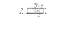
表示パネル10は、相互静電容量型のタッチ検出の基本原理に基づいて、タッチ検出を行う。また、表示パネル10は、自己静電容量型のタッチ検出の基本原理に基づいて、ホバー検出を行う。ここで、図3から図7を参照して、本実施形態の表示装置1の相互静電容量方式によるタッチ検出の基本原理について説明する。図3は、相互静電容量方式のタッチ検出の基本原理を説明するための、指がタッチしていない状態を表す説明図である。図4は、図3に示す指がタッチしていない状態の等価回路の例を示す説明図である。図5は、相互静電容量方式のタッチ検出の基本原理を説明するための、指がタッチした状態を表す説明図である。図6は、図5に示す指がタッチした状態の等価回路の例を示す説明図である。図7は、相互静電容量方式のタッチ検出の駆動信号及び検出信号の波形の一例を表す図である。なお、図6は、検出回路を併せて示している。また、以下の説明では、被検出体として指がタッチする場合を説明するが、被検出体は指に限られず、例えばスタイラスペン等の導体を含む物体であってもよい。 The
例えば、図3に示すように、容量素子C1は、誘電体Dを挟んで互いに対向配置された一対の電極、駆動電極E1及び検出電極E2を備える。図4に示すように、容量素子C1は、その一端が交流信号源(駆動信号源)Sに接続され、他端は電圧検出器DETに接続される。電圧検出器DETは、例えば図2に示す検出信号増幅部42に含まれる積分回路である。 For example, as shown in FIG. 3, the capacitive element C <b> 1 includes a pair of electrodes, a drive electrode E <b> 1, and a detection electrode E <b> 2 that are disposed to face each other with the dielectric D interposed therebetween. As shown in FIG. 4, the capacitive element C1 has one end connected to an AC signal source (drive signal source) S and the other end connected to a voltage detector DET. The voltage detector DET is an integration circuit included in the detection
交流信号源Sから駆動電極E1(容量素子C1の一端)に所定の周波数(例えば数kHzから数百kHz程度)の交流矩形波Sgが印加されると、検出電極E2(容量素子C1の他端)側に接続された電圧検出器DETを介して、図7に示すような出力波形(検出信号Vdet1)が現れる。なお、交流矩形波Sgは、駆動電極ドライバ14から入力される駆動信号Vcomに相当するものである。 When an AC rectangular wave Sg having a predetermined frequency (for example, about several kHz to several hundred kHz) is applied from the AC signal source S to the drive electrode E1 (one end of the capacitive element C1), the detection electrode E2 (the other end of the capacitive element C1) The output waveform (detection signal Vdet1) as shown in FIG. 7 appears through the voltage detector DET connected to the) side. The AC rectangular wave Sg corresponds to the drive signal Vcom input from the drive electrode driver 14.
指が表示面に接触していない状態又は接触と同視し得るほどには近接していない状態(非接触状態)では、図3及び図4に示すように、容量素子C1に対する充放電に伴って、容量素子C1の容量値に応じた電流I0が流れる。図4に示す電圧検出器DETは、交流矩形波Sgに応じた電流I0の変動を電圧の変動(実線の波形V0(図7参照))に変換する。In a state where the finger is not in contact with the display surface or in a state where the finger is not close enough to be equated with contact (non-contact state), as shown in FIGS. A current I0 corresponding to the capacitance value of the capacitive element C1 flows. The voltage detector DET shown in FIG. 4 converts the fluctuation of the current I0 according to the AC rectangular wave Sg into the fluctuation of the voltage (solid line waveform V0 (see FIG. 7)).
一方、指が接触又は近接した状態(接触状態)では、図5に示すように、指によって形成される静電容量C2が、検出電極E2と接触している又は近傍にあることにより、駆動電極E1及び検出電極E2の間にあるフリンジ分の静電容量が遮られる。このため、容量素子C1は、図6に示すように、非接触状態での容量値よりも容量値の小さい容量素子C11として作用する。そして、図6に示す等価回路でみると、容量素子C11に電流I1が流れる。On the other hand, in a state where the finger is in contact with or in close proximity (contact state), as shown in FIG. 5, the capacitance C2 formed by the finger is in contact with or in the vicinity of the detection electrode E2, so that the drive electrode The fringe capacitance between E1 and the detection electrode E2 is blocked. For this reason, the capacitive element C1 acts as a capacitive element C11 having a smaller capacitance value than the capacitance value in the non-contact state as shown in FIG. When seen in the equivalent circuit shown in FIG. 6, the current I1 flows through the capacitor C11.
図7に示すように、電圧検出器DETは、交流矩形波Sgに応じた電流I1の変動を電圧の変動(点線の波形V1)に変換する。この場合、波形V1は、上述した波形V0と比べて振幅が小さくなる。これにより、波形V0と波形V1との電圧差分の絶対値|ΔV|は、指などの外部から接触又は近接する導体の影響に応じて変化することになる。なお、電圧検出器DETは、波形V0と波形V1との電圧差分の絶対値|ΔV|を精度よく検出するため、回路内のスイッチングにより、交流矩形波Sgの周波数に合わせて、コンデンサの充放電をリセットする期間Resetを設けた動作とすることがより好ましい。As shown in FIG. 7, the voltage detector DET converts the fluctuation of the current I1 according to the AC rectangular wave Sg into the fluctuation of the voltage (dotted line waveform V1 ). In this case, the waveform V1 has a smaller amplitude than the waveform V0 described above. As a result, the absolute value | ΔV | of the voltage difference between the waveform V0 and the waveform V1 changes according to the influence of a conductor that is in contact with or close to the outside such as a finger. Note that the voltage detector DET accurately detects the absolute value | ΔV | of the voltage difference between the waveform V0 and the waveform V1 , so that the capacitance of the capacitor is adjusted according to the frequency of the AC rectangular wave Sg by switching in the circuit. More preferably, the operation is provided with a reset period during which the charge / discharge is reset.
図1に示すタッチセンサ30は、駆動電極ドライバ14から供給される駆動信号Vcomに従って、1検出ブロックずつ順次走査して、相互静電容量方式によるタッチ検出を行う。また、タッチセンサ30は、後述する複数のタッチ検出電極TDから、図4又は図6に示した電圧検出器DETを介して、検出ブロック毎に検出信号Vdet1を出力する。検出信号Vdet1は、検出部40の検出信号増幅部42に供給される。 The
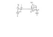
次に、図8から図11を参照して、自己静電容量方式のタッチ検出の基本原理について説明する。図8は、自己静電容量方式のタッチ検出の基本原理を説明するための、指がタッチしていない状態を表す説明図である。図9は、自己静電容量方式のタッチ検出の基本原理を説明するための、指がタッチした状態を表す説明図である。図10は、自己静電容量方式のタッチ検出の等価回路の例を示す説明図である。図11は、自己静電容量方式のタッチ検出の駆動信号及び検出信号の波形の一例を表す図である。 Next, the basic principle of the self-capacitance type touch detection will be described with reference to FIGS. FIG. 8 is an explanatory diagram showing a state where the finger is not touching, for explaining the basic principle of the self-capacitance type touch detection. FIG. 9 is an explanatory diagram showing a state in which a finger is touched, for explaining the basic principle of self-capacitance type touch detection. FIG. 10 is an explanatory diagram illustrating an example of an equivalent circuit for self-capacitance touch detection. FIG. 11 is a diagram illustrating an example of a drive signal and a detection signal waveform of the self-capacitance type touch detection.
自己静電容量方式では、上述の駆動電極E1が検出電極となる。図8左図は、指がタッチしていない状態において、スイッチング素子SW1により電源Vddと検出電極E1とが接続され、スイッチング素子SW2により検出電極E1がコンデンサCcrに接続されていない状態を示している。この状態では、検出電極E1が有する静電容量Cx1が充電される。図8右図は、スイッチング素子SW1により、電源Vddと検出電極E1との接続がオフされ、スイッチング素子SW2により、検出電極E1とコンデンサCcrとが接続された状態を示している。この状態では、静電容量Cx1の電荷はコンデンサCcrを介して放電される。 In the self-capacitance method, the drive electrode E1 described above serves as a detection electrode. The left diagram in FIG. 8 shows a state where the power supply Vdd and the detection electrode E1 are connected by the switching element SW1 and the detection electrode E1 is not connected to the capacitor Ccr by the switching element SW2 in a state where the finger is not touching. . In this state, the capacitance Cx1 included in the detection electrode E1 is charged. The right diagram in FIG. 8 shows a state in which the connection between the power supply Vdd and the detection electrode E1 is turned off by the switching element SW1, and the detection electrode E1 and the capacitor Ccr are connected by the switching element SW2. In this state, the electric charge of the capacitance Cx1 is discharged through the capacitor Ccr.
図9左図は、指がタッチした状態において、スイッチング素子SW1により電源Vddと検出電極E1とが接続され、スイッチング素子SW2により検出電極E1がコンデンサCcrに接続されていない状態を示している。この状態では、検出電極E1が有する静電容量Cx1に加え、検出電極E1に近接している指により生じる静電容量Cx2も充電される。図9右図は、スイッチング素子SW1により、電源Vddと検出電極E1との接続がオフされ、スイッチング素子SW2により検出電極E1とコンデンサCcrとが接続された状態を示している。この状態では、静電容量Cx1の電荷と静電容量Cx2の電荷とがコンデンサCcrを介して放電される。 The left diagram in FIG. 9 shows a state where the power source Vdd and the detection electrode E1 are connected by the switching element SW1 and the detection electrode E1 is not connected to the capacitor Ccr by the switching element SW2 when the finger is touched. In this state, in addition to the capacitance Cx1 included in the detection electrode E1, the capacitance Cx2 generated by the finger close to the detection electrode E1 is also charged. The right diagram in FIG. 9 shows a state where the connection between the power source Vdd and the detection electrode E1 is turned off by the switching element SW1, and the detection electrode E1 and the capacitor Ccr are connected by the switching element SW2. In this state, the electric charge of the electrostatic capacity Cx1 and the electric charge of the electrostatic capacity Cx2 are discharged through the capacitor Ccr.
ここで、図8右図に示す放電時(指がタッチしていない状態)におけるコンデンサCcrの電圧変化特性に対して、図9右図に示す放電時(指がタッチした状態)におけるコンデンサCcrの電圧変化特性は、静電容量Cx2が存在するために、明らかに異なる。したがって、自己静電容量方式では、コンデンサCcrの電圧変化特性が、静電容量Cx2の有無により、異なることを利用して、指などの操作入力の有無を判断している。 Here, with respect to the voltage change characteristic of the capacitor Ccr at the time of discharging shown in the right diagram of FIG. 8 (when the finger is not touched), the capacitor Ccr at the time of discharging shown in the right diagram of FIG. The voltage change characteristics are clearly different due to the presence of the capacitance Cx2. Therefore, in the self-capacitance method, the presence / absence of an operation input such as a finger is determined using the fact that the voltage change characteristic of the capacitor Ccr varies depending on the presence / absence of the capacitance Cx2.
具体的には、検出電極E1に所定の周波数(例えば数kHzから数百kHz程度)の交流矩形波Sg(図11参照)が印加される。図10に示す電圧検出器DETは、交流矩形波Sgに応じた電流の変動を電圧の変動(波形V4、V5)に変換する。Specifically, an AC rectangular wave Sg (see FIG. 11) having a predetermined frequency (for example, about several kHz to several hundred kHz) is applied to the detection electrode E1. The voltage detector DET shown in FIG. 10 converts a current fluctuation according to the AC rectangular wave Sg into a voltage fluctuation (waveforms V4 and V5 ).
上述のように、検出電極E1はスイッチング素子SW1及びスイッチング素子SW2によって電源Vdd及びコンデンサCcrから切り離すことが可能な構成となっている。図11において、時刻T01のタイミングで交流矩形波Sgは電圧V0に相当する電圧レベルを上昇させる。このときスイッチング素子SW1はオンしておりスイッチング素子SW2はオフしている。このため検出電極E1の電圧も電圧V0に上昇する。次に時刻T11のタイミングの前にスイッチング素子SW1をオフとする。このとき検出電極E1は、電気的にどことも接続されていない状態、すなわちフローティングであるが、検出電極E1の静電容量Cx1(図8参照)、あるいは検出電極E1の静電容量Cx1に指等のタッチによる静電容量Cx2を加えた容量(Cx1+Cx2、図9参照)によって、検出電極E1の電位はV0が維持される。さらに、時刻T11のタイミングの前にスイッチング素子SW3をオンさせ所定の時間経過後にオフさせ電圧検出器DETをリセットさせる。このリセット動作により出力電圧は基準電圧Vrefと略等しい電圧となる。As described above, the detection electrode E1 can be disconnected from the power supply Vdd and the capacitor Ccr by the switching element SW1 and the switching element SW2. In FIG. 11, the AC rectangular wave Sg increases the voltage level corresponding to the voltage V0 at the timing of time T01 . At this time, the switching element SW1 is on and the switching element SW2 is off. Therefore the voltage of the detection electrodes E1 also rises to the voltage V0. Then turning off the switching element SW1 in front of the timing of timeT 11. At this time, the detection electrode E1 is electrically connected to nowhere, that is, is floating, but the capacitance Cx1 (see FIG. 8) of the detection electrode E1 or the capacitance Cx1 of the detection electrode E1 is a finger or the like. The potential of the detection electrode E1 is maintained at V0 by the capacitance (Cx1 + Cx2, see FIG. 9) including the capacitance Cx2 due to the touch. Furthermore, to reset the voltage detector DET is turned off after a predetermined time to turn on the switching elements SW3 before the timing of time T11. By this reset operation, the output voltage becomes substantially equal to the reference voltage Vref.
続いて、時刻T11のタイミングでスイッチング素子SW2をオンさせると、電圧検出器DETの反転入力部が検出電極E1の電圧V0となり、その後、検出電極E1の静電容量Cx1(または、Cx1+Cx2)と電圧検出器DET内の静電容量C5の時定数に従って電圧検出器DETの反転入力部は基準電圧Vrefまで低下する。このとき、検出電極E1の静電容量Cx1(または、Cx1+Cx2)に蓄積されていた電荷が電圧検出器DET内の静電容量C5に移動するため、電圧検出器DETの出力が上昇する(Vdet2)。電圧検出器DETの出力(Vdet2)は、検出電極E1に指等がタッチしていないときは、実線で示す波形V4となり、Vdet2=Cx1×V0/C5となる。指等の影響による容量が付加されたときは、点線で示す波形V5となり、Vdet2=(Cx1+Cx2)×V0/C5となる。Subsequently, when turning on the switching element SW2 at timeT 11, next to the voltageV 0 which inverting input is the detection electrode E1 of the voltage detector DET, then the electrostatic capacitance of the detection electrodes E1 Cx1 (or, Cx1 + Cx2) In accordance with the time constant of the capacitance C5 in the voltage detector DET, the inverting input portion of the voltage detector DET is reduced to the reference voltage Vref. At this time, the charge accumulated in the capacitance Cx1 (or Cx1 + Cx2) of the detection electrode E1 moves to the capacitance C5 in the voltage detector DET, so that the output of the voltage detector DET increases (Vdet2). . The output of the voltage detector DET (Vdet2) when the finger or the like to the detection electrodes E1 are not touched, next waveformV 4 shown by a solid line, andVdet2 = Cx1 × V 0 / C5 . When the capacity due to the influence of such a finger is added, it becomes a waveformV 5 shown by a dotted line, the Vdet2 = (Cx1 + Cx2) ×
その後、検出電極E1の静電容量Cx1(または、Cx1+Cx2)の電荷が静電容量C5に十分移動した後の時刻T31のタイミングでスイッチング素子SW2をオフさせ、スイッチング素子SW1及びスイッチング素子SW3をオンさせることにより、検出電極E1の電位を交流矩形波Sgと同電位のローレベルにするとともに電圧検出器DETをリセットさせる。なお、このとき、スイッチング素子SW1をオンさせるタイミングは、スイッチング素子SW2をオフさせた後、時刻T02以前であればいずれのタイミングでもよい。また、電圧検出器DETをリセットさせるタイミングは、スイッチング素子SW2をオフさせた後、時刻T12以前であればいずれのタイミングとしてもよい。On Thereafter, the capacitance Cx1 detection electrodes E1 (or, Cx1 + Cx2) charge of turns off the switching element SW2 at timeT 31 after sufficiently moved to the capacitance C5, the switching element SW1 and switching devices SW3 As a result, the potential of the detection electrode E1 is set to a low level that is the same potential as the AC rectangular wave Sg, and the voltage detector DET is reset. At this time, the timing for turning on the switching element SW1 may be any timing before the timeT02 after the switching element SW2 is turned off. The timing for resetting the voltage detector DET is, after off the switching element SW2, may be any timing as long as the time T12 before.
以上の動作を所定の周波数(例えば数kHzから数百kHz程度)で繰り返す。波形V4と波形V5との差分の絶対値|ΔV|に基づいて、外部近接物体の有無(タッチの有無)を測定することができる。なお、検出電極E1の電位は、図11に示すように、指等がタッチしていないときはV2の波形となり、指等の影響による静電容量Cx2が付加されるときはV3の波形となる。波形V2と波形V3とが、それぞれ所定の閾値電圧VTHまで下がる時間を測定することにより外部近接物体の有無(タッチの有無)を測定することも可能である。The above operation is repeated at a predetermined frequency (for example, about several kHz to several hundred kHz). Based on the absolute value | ΔV | of the difference between the waveform V4 and the waveform V5 , the presence or absence of an external proximity object (the presence or absence of a touch) can be measured. The potential of the detecting electrode E1, as shown in FIG. 11, when the finger or the like is not touching has a waveform of V2, the waveform of V3 when the electrostatic capacitance Cx2 due to the influence of a finger or the like is added It becomes. It is also possible to measure the presence / absence of an external proximity object (the presence / absence of touch) by measuring the time during which the waveform V2 and the waveform V3 drop to a predetermined threshold voltage VTH .
図1に示すタッチセンサ30は、駆動電極ドライバ14から供給される駆動信号Vcomに従って、自己静電容量方式によるホバー検出を行う。また、タッチセンサ30は、後述する駆動電極CDから、図10に示す電圧検出器DETを介して、検出信号Vdet2を出力し、検出部40の検出信号増幅部42に供給する。 The
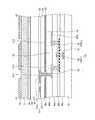
次に、表示装置1の構成例を詳細に説明する。図12は、表示パネルの構成例を示す断面図である。図13は、表示装置を構成するTFT基板を模式的に示す平面図である。図12に示すように、表示パネル10は、第1基板2と、第1基板2の表面に垂直な方向に対向して配置された第2基板3と、第1基板2と第2基板3との間に配置された液晶層6とを備える。 Next, a configuration example of the
図12に示すように、第1基板2は、回路基板としてのTFT(Thin Film Transistor)基板21と、TFT基板21の上方に行列状(マトリクス状)に配設された複数の画素電極22と、TFT基板21と画素電極22との間に設けられた複数の駆動電極CDと、画素電極22と駆動電極CDとを絶縁する絶縁層24と、を有する。TFT基板21の下側には、接着層(図示しない)を介して偏光板35Bが設けられている。なお、本明細書では、TFT基板21に垂直な方向において、TFT基板21から対向基板31に向かう方向を「上側」ともいう。また、対向基板31からTFT基板21に向かう方向を「下側」ともいう。 As shown in FIG. 12, the
図13に示すように、TFT基板21は、画像を表示させるための表示領域10aと、表示領域10aの周囲に設けられた額縁領域10bとを有する。表示領域10aは、一対の長辺と短辺とを有する矩形状である。額縁領域10bは、表示領域10aの4辺を囲む枠状となっている。 As shown in FIG. 13, the
複数の駆動電極CDは、TFT基板21の表示領域10aに設けられており、表示領域10aの長辺に沿った方向及び短辺に沿った方向に、行列状に複数配列されている。駆動電極CDは、例えば、ITO(Indium Tin Oxide)等の透光性を有する導電性材料で構成されている。1つの駆動電極CDに対応する位置に、複数の画素電極22が行列状に配置される。画素電極22は、駆動電極CDよりも小さい面積を有する。なお、図13では一部の駆動電極CD及び画素電極22について示しているが、駆動電極CD及び画素電極22は表示領域10aの全域に亘って配置される。なお、本明細書では、行方向をX方向ともいい、列方向をY方向ともいう。またX方向を第1方向、Y方向を第2方向とする。 The plurality of drive electrodes CD are provided in the
TFT基板21の額縁領域10bには、表示用IC19が配置されている。表示用IC19は、TFT基板21にCOG(Chip On Glass)実装されたチップである。図1に示した制御部11は、例えば、表示用IC19に内蔵されている。表示用IC19は、データ線SGL(図14参照)及びゲート線GCL(図14参照)にそれぞれ接続している。また、表示用IC19は、例えば、後述の接続切替回路17(図21参照)を介して、複数の駆動電極CDにそれぞれ接続している。表示用IC19は、外部のホストIC(図示しない)から供給された映像信号Vdisp(図1参照)に基づいて、後述するゲート線GCL及びデータ線SGL等に制御信号を出力する。なお、本実施形態では、制御部11の少なくとも一部が、表示用IC19以外の他のICに内蔵されていてもよい。他のICは、TFT基板21にCOG実装されたチップであってもよいし、TFT基板21に接続するフレキシブル基板に実装されたチップであってもよい。 A
図13に示すように、表示用IC19は、例えば、額縁領域10bの短辺側に配置されていてもよい。これによれば、額縁領域10bの長辺側に表示用IC19を設ける必要がなく、額縁領域10bの長辺側の幅を小さくすることができる。 As shown in FIG. 13, the
図12に示すように、第2基板3は、対向 基板31と、対向基板31の一方の面に設けられたカラーフィルタ32とを有する。対向基板31の他方の面には、タッチセンサ30(図1参照)のタッチ検出電極TDが設けられている。さらに、タッチ検出電極TDの上方には、接着層(図示しない)を介して偏光板35Aが設けられている。また、対向基板31には、フレキシブル基板71(図18参照)が接続されている。フレキシブル基板71は配線を介してタッチ検出電極TDに接続される。 As shown in FIG. 12, the
図12に示すように、TFT基板21と対向基板31は、所定の間隔を設けて対向して配置される。TFT基板21と対向基板31との間の空間に、表示機能層として液晶層6が設けられる。液晶層6は、電界の状態に応じてそこを通過する光を変調するものであり、例えば、FFS(フリンジフィールドスイッチング)を含むIPS(インプレーンスイッチング)等の横電界モードの液晶が用いられる。なお、図12に示す液晶層6と第1基板2との間、及び液晶層6と第2基板3との間には、それぞれ配向膜が設けられている。 As shown in FIG. 12, the
図14は、実施形態1に係る表示部の画素配列を表す回路図である。図15は、副画素の構成例を示す平面図である。図16は、図15のA1−A2線に沿う断面図である。図12に示すTFT基板21には、図14に示す各副画素SPixのスイッチング素子TrD、各画素電極22に画素信号Vpixを供給するデータ線SGL、各スイッチング素子TrDを駆動する駆動信号を供給するゲート線GCL等の配線が設けられている。データ線SGL及びゲート線GCLは、TFT基板21の表面と平行な平面に延在している。 FIG. 14 is a circuit diagram illustrating a pixel array of the display unit according to the first embodiment. FIG. 15 is a plan view illustrating a configuration example of subpixels. 16 is a cross-sectional view taken along line A1-A2 of FIG. The
図14に示す表示部20は、行列状に配列された複数の副画素SPixを有する。副画素SPixは、それぞれスイッチング素子TrD及び液晶素子LCを備える。スイッチング素子TrDは、薄膜トランジスタで構成されるものであり、この例では、nチャネルのMOS(Metal Oxide Semiconductor)型のTFTで構成されている。スイッチング素子TrDのソースはデータ線SGLに接続され、ゲートはゲート線GCLに接続され、ドレインは液晶素子LCの一端に接続されている。液晶素子LCの他端は、駆動電極CDに接続されている。また、画素電極22と駆動電極CDとの間に絶縁層24(図11参照)が設けられており、これにより図14に示す保持容量Csが形成される。 The
副画素SPixは、ゲート線GCLにより、表示部20の同じ行に属する他の副画素SPixと互いに接続されている。ゲート線GCLは、ゲートドライバ12(図1参照)と接続され、ゲートドライバ12より走査信号Vscanが供給される。また、副画素SPixは、データ線SGLにより、表示部20の同じ列に属する他の副画素SPixと互いに接続されている。データ線SGLは、ソースドライバ13(図1参照)と接続され、ソースドライバ13より画素信号Vpixが供給される。駆動電極CDは、駆動電極ドライバ14(図1参照)と接続され、駆動電極ドライバ14から表示用の駆動信号Vcomdc又は検出用の駆動信号Vcomが供給される。 The subpixel SPix is connected to another subpixel SPix belonging to the same row of the
図15に示すように、ゲート線GCLとデータ線SGLとで囲まれた領域が副画素SPixである。副画素SPixは、画素電極22と駆動電極CDとが重なる領域を含んで設けられる。複数の画素電極22は、それぞれスイッチング素子TrDを介してデータ線SGLと接続される 。 As shown in FIG. 15, a region surrounded by the gate line GCL and the data line SGL is a subpixel SPix. The subpixel SPix is provided including a region where the
図15に示すように、画素電極22は、複数の帯状電極22aと、連結部22bとを有する。帯状電極22aは、データ線SGLに沿って設けられ、ゲート線GCLに沿った方向に複数配列されている。連結部22bは帯状電極22aの端部同士を連結する。なお、画素電極22は、5本の帯状電極22aを有するが、これに限定されず、4本以下又は6本以上の帯状電極22aを有していてもよい。例えば、画素電極22は、2本の帯状電極22aを有していてもよい。 As shown in FIG. 15, the
図15に示すように、スイッチング素子TrDは、半導体層61、ソース電極62、ドレイン電極63及びゲート電極64を含む。また、半導体層61の下側に遮光層65が設けられている。例えば、バックライトから半導体層61に向かう光は、遮光層65によって遮光される。 As shown in FIG. 15, the switching element TrD includes a
図16に示すように、遮光層65は基板121の上に設けられている。絶縁層58aは、遮光層65を覆って基板121の上に設けられている。絶縁層58aの上には半導体層61が設けられている。半導体層61の上側に絶縁層58bを介して、ゲート電極64(ゲート線GCL)が設けられている。ゲート電極64(ゲート線GCL)の上側に絶縁層58cを介してドレイン電極63及びソース電極62(データ線SGL)が設けられる。ドレイン電極63及びソース電極62(データ線SGL)の上側に絶縁層58dを介して、駆動電極CDが設けられる。上述のように駆動電極CDの上側に絶縁層24を介して画素電極22が設けられる。画素電極22の上には配向膜34が設けられる。また、液晶層6を挟んで配向膜34と対向する側に配向膜33が設けられる。 As shown in FIG. 16, the
図15及び図16に示すように、画素電極22は、コンタクトホールH11を介してスイッチング素子TrDのドレイン電極63と接続されている。半導体層61は、コンタクトホールH12を介してドレイン電極63に接続される。半導体層61は、平面視 でゲート電極64と交差する。本明細書において、平面視とは、表示パネル10の厚さ方向(Z方向)から見ることを意味する。ゲート電極64はゲート線GCLに接続され、ゲート線GCLの一辺から突出している。半導体層61は、ソース電極62と重畳する位置まで延びて、コンタクトホールH13を介してソース電極62と電気的に接続される。ソース電極62は、データ線SGLに接続され、データ線SGLの一辺から突出している。 As shown in FIGS. 15 and 16, the
ゲートドライバ12(図1参照)は、ゲート線GCLを順次走査するように駆動する。ゲートドライバ12は、ゲート線GCLを介して、走査信号Vscan(図1参照)を副画素SPixのTFT素子Trのゲートに印加することにより、副画素SPixのうちの1行(1水平ライン)を表示駆動の対象として順次選択する。また、ソースドライバ13は、ゲートドライバ12によって選択された1水平ラインに属する副画素SPixに対して、図14に示すデータ線SGLを介して、画素信号Vpixを供給する。そして、副画素SPixでは、供給される画素信号Vpixに応じて1水平ラインずつ表示が行われる。この表示動作を行う際、駆動電極ドライバ14は、駆動電極CDに表示用の駆動信号Vcomdcを印加する。これにより、駆動電極CDは、表示部20の複数の画素電極22に対し共通の電位(基準電位)を与える共通電極として機能する。 The gate driver 12 (see FIG. 1) is driven so as to sequentially scan the gate lines GCL. The
なお、本実施形態では、駆動電極CDは、タッチセンサ30の相互静電容量方式によるタッチ検出を行う際の駆動電極としても機能する。また、駆動電極CDは、タッチセンサ30の自己静電容量方式によるホバー検出を行う際の検出電極としても機能する。 In the present embodiment, the drive electrode CD also functions as a drive electrode when performing touch detection of the
カラーフィルタ32は、例えば、赤(R)、緑(G)、青(B)の3色に着色されたカラーフィルタの色領域が周期的に配列されている。各副画素SPixに、R、G、Bの3色の色領域32R、32G、32Bが1組として対応付けられ、3色の色領域32R、32G、32Bに対応する副画素SPixを1組として画素Pixが構成される。カラーフィルタ32は、TFT基板21と垂直な方向において、液晶層6と対向する。なお、カラーフィルタ32は、異なる色に着色されていれば、他の色の組み合わせであってもよい。また、カラーフィルタ32は、3色の組み合わせに限定されず、4色以上の組み合わせであってもよい。 In the
表示装置1は、例えば、検出動作(検出動作期間)と表示動作(表示動作期間)とを時分割に行う。表示装置1は、検出動作と表示動作とをどのように分けて行ってもよい。以下では、表示装置1が、表示部20の1フレーム期間(1F期間)、すなわち、一画面分の映像情報が表示されるのに要する時間の中において、検出動作と表示動作とをそれぞれ複数回に分割して行う方法について説明する。 For example, the
図17は、1フレーム期間における表示動作期間と検出動作期間の配置の一例を表す模式図である。1フレーム期間(1F)は、2つの表示動作期間Pd1、Pd2及び2つの検出動作期間Pt1、Pt2からなる。これらの各期間は、時間軸上において、表示動作期間Pd1、検出動作期間Pt1、表示動作期間Pd2、検出動作期間Pt2のように交互に配置されている。 FIG. 17 is a schematic diagram illustrating an example of the arrangement of the display operation period and the detection operation period in one frame period. One frame period (1F) includes two display operation periods Pd1 and Pd2 and two detection operation periods Pt1 and Pt2. These periods are alternately arranged on the time axis as a display operation period Pd1, a detection operation period Pt1, a display operation period Pd2, and a detection operation period Pt2.
制御部11(図1参照)は、ゲートドライバ12とソースドライバ13とを介して、各表示動作期間Pd1、Pd2に選択される複数行の画素Pix(図14参照)に画素信号Vpixを供給する。制御部11は、各表示動作期間Pd1、Pd2においては、駆動電極ドライバ14を介して選択される駆動電極CDに、表示用の共通電極電位である表示用の駆動信号Vcomdcを供給する。 The control unit 11 (see FIG. 1) supplies the pixel signal Vpix to the plurality of rows of pixels Pix (see FIG. 14) selected in the display operation periods Pd1 and Pd2 via the
また、各検出動作期間Pt1、Pt2は、タッチ検出電極TDと駆動電極CDとの間の相互静電容量の変化に基づいてタッチ検出を行うタッチ検出期間、及び、駆動電極CDの自己静電容量の変化に基づいてホバー検出を行うホバー検出期間、をそれぞれ有する。タッチ検出期間では、制御部11(図1参照)は、駆動電極ドライバ14を介して、各タッチ検出期間に選択される駆動電極CDに、検出用の駆動信号Vcomを供給する。検出部40は、タッチ検出電極TDから供給される検出信号Vdet1に基づいて、タッチの有無及びタッチ入力位置の座標の演算を行う。一方、ホバー検出期間では、制御部11は、駆動電極ドライバ14を介して、各駆動電極CDに検出用の駆動信号Vcomを供給する。検出部40は、各駆動電極CDから供給される検出信号Vdet2に基づいて、ホバーの有無及びホバー入力位置の座標の演算を行う。 Each detection operation period Pt1 and Pt2 includes a touch detection period in which touch detection is performed based on a change in mutual capacitance between the touch detection electrode TD and the drive electrode CD, and a self-capacitance of the drive electrode CD. Each has a hover detection period in which hover detection is performed based on the change in. In the touch detection period, the control unit 11 (see FIG. 1) supplies a drive signal Vcom for detection to the drive electrode CD selected in each touch detection period via the drive electrode driver 14. The
図17に示す例では、表示装置1は、1フレーム期間(1F)において1画面分の映像表示を2回に分けて行うが、1フレーム期間(1F)内の表示動作期間はさらに多くの回数に分けられていてもよい。検出動作期間についても、1フレーム期間(1F)中にさらに多くの回数が設けられていてもよい。 In the example shown in FIG. 17, the
表示装置1は、検出動作期間Pt1、Pt2において、それぞれ一画面の半分ずつの検出を行ってもよく、また、それぞれ一画面分の検出を行ってもよい。また、表示装置1は、検出動作期間Pt1、Pt2において、必要に応じて間引き検出等を行ってもよい。また、表示装置1は、1フレーム期間(1F)中の表示動作と検出動作とを複数回に分けずに1回ずつ行ってもよい。 In the detection operation periods Pt1 and Pt2, the
検出動作期間Pt1、Pt2において、表示装置1は、ゲート線GCL及びデータ線SGL(図14参照)を、電圧信号が供給されず、電気的にどことも接続されていない状態(Hi−Z:ハイインピーダンス)としてもよい。または、表示装置1は、ゲート線GCL及びデータ線SGLに、検出用の駆動信号Vcomと同じ波形で、かつ駆動信号Vcomに同期したガード信号Vgdを供給してもよい。これによれば、検出動作期間Pt1、Pt2において、ゲート線GCL及びデータ線SGLと、検出用の駆動信号Vcomが供給される駆動電極CDとの間に静電容量が生じることを防ぐことができるので、検出の感度を高めることができる。 In the detection operation periods Pt1 and Pt2, the
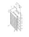
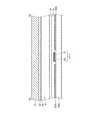
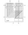
図18は、実施形態1に係る表示パネルの駆動電極及びタッチ検出電極の構成例を示す斜視図である。また、図19は、図18に示す表示パネルを側方から見た図である。図18及び図19に示すように、タッチセンサ30は、TFT基板21に設けられた複数の駆動電極CDと、対向基板31に設けられた複数のタッチ検出電極TDと、カバーガラス81と、を有する。例えば、TFT基板21は、第1面21aと、第1面21aの反対側に位置する第2面21bとを有する。また、対向基板31は、第1面31aと、第1面31aの反対側に位置する第2面31bとを有する。そして、TFT基板21の第1面21aと、対向基板31の第2面31bとが向かい合っている。複数の駆動電極CDはTFT基板21の第1面21aに設けられており、複数のタッチ検出電極TDは対向基板31の第2面31bに設けられている。複数の駆動電極CD及び複数のタッチ検出電極TDは、いずれも表示領域10aに設けられている。 FIG. 18 is a perspective view illustrating a configuration example of drive electrodes and touch detection electrodes of the display panel according to the first embodiment. FIG. 19 is a side view of the display panel shown in FIG. As shown in FIGS. 18 and 19, the
駆動電極CDの平面視による形状は、例えば四角形である。また、タッチ検出電極TDの平面視による形状も、例えば四角形である。四角形として、例えば、正方形又は矩形が挙げられる。平面視で、駆動電極CDはタッチ検出電極TDよりも大きい。また、複数の駆動電極CDそれぞれは、複数のタッチ検出電極TDと平面視で重なっている。例えば、1個の駆動電極CDは、複数のタッチ検出電極TDと平面視で重なっている。タッチ検出電極TDと駆動電極CDとが重なる部分に静電容量が形成される。 The shape of the drive electrode CD in plan view is, for example, a quadrangle. Further, the shape of the touch detection electrode TD in plan view is, for example, a quadrangle. Examples of the quadrangle include a square or a rectangle. In plan view, the drive electrode CD is larger than the touch detection electrode TD. In addition, each of the plurality of drive electrodes CD overlaps with the plurality of touch detection electrodes TD in plan view. For example, one drive electrode CD overlaps with the plurality of touch detection electrodes TD in plan view. A capacitance is formed in a portion where the touch detection electrode TD and the drive electrode CD overlap.
また、TFT基板21の額縁領域10bにフレキシブル基板71の一端が接続され、対向基板31の額縁領域10bにフレキシブル基板71の他端が接続されている。また、TFT基板21の額縁領域10bにフレキシブル基板73の一端が接続されている。図18及び図19に示すように、フレキシブル基板73には、例えば、検出部40(図1参照)を内蔵する検出用IC75が実装されている。タッチ検出電極TDは、フレキシブル基板71、73にそれぞれ設けられた配線を介して、検出部40の検出信号増幅部42(図2参照)の入力に接続される。駆動電極CDは、フレキシブル基板73に設けられた配線を介して、検出部40の検出信号増幅部42の入力に接続される。 One end of the
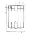
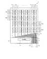
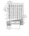
次に、第1基板2及び第2基板3の構成例について、より具体的に説明する。図20は、第2基板の第1構成例を示す平面図である。図20に示すように、第2基板3は、タッチ検出電極TDとして、タッチ検出電極TD1、TD2、TD3及びTD4を有する。図20に示す例では、タッチ検出電極TD1、TD2、TD3及びTD4は、それぞれ16個ずつ設けられている。タッチ検出電極TD1、TD2、TD3及びTD4は互いに同一の形状で、かつ同一の大きさである。タッチ検出電極TD1、TD2、TD3及びTD4は、行方向及び列方向にそれぞれ一定の間隔で並んで配置されている。なお図20では、タッチ検出電極TDとして4つのタッチ検出電極TD1からTD4について述べているが、タッチ検出電極TDの数はこれに限定されない。タッチ検出電極TDとして、複数の電極が設けられていればよい。さらに好ましくは、行方向及び列方向に対して、同じ数のタッチ検出電極TDが設けられていればよい。 Next, configuration examples of the
例えば、対向基板31の行方向において、タッチ検出電極TD1、TD3が互いに隣り合うとともに、タッチ検出電極TD2、TD4が互いに隣り合っている。また、列方向において、タッチ検出電極TD1、TD2が互いに隣り合うとともに、タッチ検出電極TD3、TD4が互いに隣り合っている。図20に示す例では、4個のタッチ検出電極TD1、TD2、TD3及びTD4が、1個のタッチ検出電極ブロックTDBを構成している。そして、16個のタッチ検出電極ブロックTDBが、行方向及び列方向にそれぞれ一定の間隔で並んで配置されている。 For example, in the row direction of the
また、第2基板3は、対向基板31の第1面31aに設けられた16本の配線37−1から37−16を有する。複数の配線37−1から37−16は、タッチ検出電極TD1、TD2、TD3及びTD4のいずれか1つに接続し、表示領域10a(図18参照)から額縁領域10b(図18参照)まで引き出されている。例えば、配線37−1はタッチ検出電極TD1に接続し、配線37−2はタッチ検出電極TD2に接続し、配線37−3はタッチ検出電極TD3に接続し、配線37−4はタッチ検出電極TD4に接続している。 The
なお、以下の説明で、タッチ検出電極TD1、TD2、TD3及びTD4、及び、後述のタッチ検出電極TD1からTD16(図26参照)を区別して説明する必要がないときは、それぞれをタッチ検出電極TDという。また、配線37−1から37−16を区別して説明する必要がないときは、それぞれを配線37という。タッチ検出電極TD及び配線37は、例えば、ITO(Indium Tin Oxide)等の透光性を有する導電性材料で構成されている。タッチ検出電極TD及び配線37は、例えば、同一の工程で同時に形成された導電層であり、同一の層に設けられている。また、タッチ検出電極TD及び配線37は、ITOに限定されず、例えば、金属材料を用いた金属細線等により構成されていてもよい。 In the following description, when it is not necessary to distinguish between the touch detection electrodes TD1, TD2, TD3, and TD4, and touch detection electrodes TD1 to TD16 (see FIG. 26) described later, the touch detection electrodes TD are respectively described. That's it. Further, when there is no need to distinguish between the wirings 37-1 to 37-16, they are referred to as
フレキシブル基板71には、16本の配線77−1から77−16が設けられている。複数の配線77−1から77−16は、対向基板31に設けられた複数の配線37−1から37−16にそれぞれ接続している。例えば、配線37−1は配線77−1に接続し、配線37−2は配線77−2に接続し、配線37−15は配線77−15に接続し、配線37−16は配線77−16に接続している。なお、以下の説明で、配線77−1から77−16を区別して説明する必要がないときは、それぞれを配線77という。配線77は、例えば、銅等の導電性材料で構成されている。 The
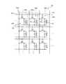
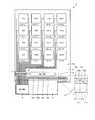
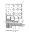
図21は、第1基板2の第1構成例を示す平面図である。図21に示すように、第1基板2は、駆動電極CDとして、例えば16個の駆動電極CD1からCD16を有する。駆動電極CD1からCD16の平面視による形状は、例えば正方形又は矩形である。駆動電極CD1からCD16は互いに同一の形状で、かつ同一の大きさであり、行方向及び列方向にそれぞれ一定の間隔で並んで配置されている。 FIG. 21 is a plan view showing a first configuration example of the
また、第1基板2は、TFT基板21の第1面21aに設けられた16本の配線27−1から27−16を有する。複数の配線27−1から27−16は、駆動電極CD1からCD16のいずれか1つに接続し、表示領域10a(図18参照)から額縁領域10b(図18参照)まで引き出されている。例えば、配線27−1は駆動電極CD1に接続し、配線27−2は駆動電極CD2に接続し、配線27−3は駆動電極CD3に接続し、配線27−4は駆動電極CD4に接続している。 The
なお、以下の説明で、駆動電極CD1からCD16を区別して説明する必要がないときは、それぞれを駆動電極CDという。また、配線27−1から27−16を区別して説明する必要がないときは、それぞれを配線27という。駆動電極CMOL及び配線27は、例えば、ITO等の透光性を有する導電性材料で構成されている。駆動電極CD及び配線27は、例えば、同一の工程で同時に形成された導電層であり、同一の層に設けられている。 In the following description, when it is not necessary to distinguish between the drive electrodes CD1 to CD16, each is referred to as a drive electrode CD. Further, when it is not necessary to distinguish between the wirings 27-1 to 27-16, each is referred to as a wiring 27. The drive electrode CMOL and the wiring 27 are made of a light-transmitting conductive material such as ITO. The drive electrode CD and the wiring 27 are, for example, conductive layers formed simultaneously in the same process, and are provided in the same layer.
また、図21に示す例では、第1基板2は、TFT基板21の第1面21aに設けられた4本の配線26A、26B、26C、26Dを有する。図20及び図21に示すように、TFT基板21の第1面21aにおいて、1本の配線26Aは、フレキシブル基板71に設けられた4本の配線77(例えば、配線77−1等)を介して、4本の配線37(例えば、配線37−1等)に接続し、16個のタッチ検出電極TD1に接続している。1本の配線26Bは、フレキシブル基板71に設けられた4本の配線77(例えば、配線77−2等)を介して、4本の配線37(例えば、配線37−2等)に接続し、16個のタッチ検出電極TD2に接続している。1本の配線26Cは、フレキシブル基板71に設けられた4本の配線77(例えば、配線77−3等)を介して、4本の配線37(例えば、配線37−3等)に接続し、16個のタッチ検出電極TD3に接続している。1本の配線26Dは、フレキシブル基板71に設けられた4本の配線77(例えば、配線77−4等)を介して、4本の配線37(例えば、配線37−4等)に接続し、16個のタッチ検出電極TD4に接続している。なお、以下の説明で、配線26Aから26D、及び、後述の配線26−1から26−16(図23参照)を区別して説明する必要がないときは、それぞれを配線26という。配線26は、例えば銅等の導電性材料で構成されている。配線26は、例えばTFT基板21の額縁領域10b(図18参照)に設けられている。 In the example illustrated in FIG. 21, the
図21に示すように、配線26は、フレキシブル基板73に設けられた配線を介して、検出用IC75に接続している。また、第1基板2は、例えば、TFT基板21に設けられた接続切替回路17と、TFT基板21に設けられて接続切替回路17と表示用IC19とを接続する配線18と、を有する。配線27は、接続切替回路17によって、表示用IC19又は検出用IC75に接続される。なお、接続切替回路17は、表示用IC19に内蔵されていてもよいし、検出用IC75に内蔵されていてもよいし、TFT基板21又はフレキシブル基板73に実装された図示しないICに内蔵されていてもよい。接続切替回路17の内部の構成例は、後で図24を参照しながら説明する。 As shown in FIG. 21, the
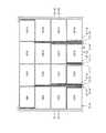
図22は、図21に示した第1基板に図20に示した第2基板を重ね合せた図である。図22に示すように、タッチ検出電極ブロックTDB は、駆動電極CDと重なるように配置されている。例えば、1個の駆動電極CDと平面視で重なる位置に、4個のタッチ検出電極TD1からTD4が配置されている。そして、これら4個のタッチ検出電極TD1からTD4から、1個のタッチ検出電極ブロックTDBが構成されている。また、1本の配線37は、駆動電極CDと平面視で重なる各位置間で、タッチ検出電極TD同士を接続している。例えば、配線37−1は、駆動電極CDと平面視で重なる各位置のタッチ検出電極TD1を列方向に接続している。配線37−2は、駆動電極CDと平面視で重なる各位置のタッチ検出電極TD2を列方向に接続している。配線37−3は、駆動電極CDと平面視で重なる各位置のタッチ検出電極TD3を列方向に接続している。配線37−4は、駆動電極CDと平面視で重なる各位置のタッチ検出電極TD4を列方向に接続している。 FIG. 22 is a diagram in which the second substrate shown in FIG. 20 is superimposed on the first substrate shown in FIG. As shown in FIG. 22, the touch detection electrode block TDB is disposed so as to overlap the drive electrode CD. For example, four touch detection electrodes TD1 to TD4 are arranged at a position overlapping with one drive electrode CD in plan view. The four touch detection electrodes TD1 to TD4 constitute one touch detection electrode block TDB. In addition, one
すなわち、複数のタッチ検出電極TD1は、異なる駆動電極CD間であっても、駆動電極CDに対する位置は互いに同じである。例えば、駆動電極CD1と平面視で重なるタッチ検出電極TD1の駆動電極CD1に対する位置と、駆動電極CD2と平面視で重なるタッチ検出電極TD1の駆動電極CD2に対する位置は、互いに同じである。同様に、複数のタッチ検出電極TD2は、異なる駆動電極CD間であっても、駆動電極CDに対する位置は互いに同じである。複数のタッチ検出電極TD3は、異なる駆動電極CD間であっても、駆動電極CDに対する位置は互いに同じである。複数のタッチ検出電極TD4は、異なる駆動電極CD間であっても、駆動電極CDに対する位置は互いに同じである。そして、1本の配線37は、異なる駆動電極CD間であっても、駆動電極CDに対する位置が互いに同じであるタッチ検出電極TD同士を接続している。例えば、配線37−1は、異なる駆動電極CD間であっても、駆動電極CDに対する位置が互いに同じであるタッチ検出電極TD1同士を接続している。配線37−2は、異なる駆動電極CD間であっても、駆動電極CDに対する位置が互いに同じであるタッチ検出電極TD2同士を接続している。配線37−3は、異なる駆動電極CD間であっても、駆動電極CDに対する位置が互いに同じであるタッチ検出電極TD3同士を接続している。配線37−4は、異なる駆動電極CD間であっても、駆動電極CDに対する位置が互いに同じであるタッチ検出電極TD4同士を接続している。 That is, the positions of the plurality of touch detection electrodes TD1 with respect to the drive electrodes CD are the same even between different drive electrodes CD. For example, the position of the touch detection electrode TD1 that overlaps the drive electrode CD1 in plan view with respect to the drive electrode CD1 is the same as the position of the touch detection electrode TD1 that overlaps the drive electrode CD2 in plan view with respect to the drive electrode CD2. Similarly, the positions of the plurality of touch detection electrodes TD2 with respect to the drive electrodes CD are the same even between different drive electrodes CD. The positions of the plurality of touch detection electrodes TD3 with respect to the drive electrodes CD are the same even between different drive electrodes CD. The positions of the plurality of touch detection electrodes TD4 with respect to the drive electrodes CD are the same even between different drive electrodes CD. One
図23は、第1基板の第2構成例を示す平面図である。図23に示すように、第1基板2は、TFT基板21に設けられる配線26として、16本の配線26−1から26−16を有してもよい。これによれば、TFT基板21に設けられた16本の配線26−1から26−16を、図20に示したフレキシブル基板71の配線77を介して、16本の配線37−1から37−6と1本ずつ接続することができる。これにより、タッチ検出電極TD1を列ごとに4個ずつ接続して、それぞれ独立した配線を介して、検出用ICに接続することができる。また、タッチ検出電極TD2を列ごとに4個ずつ接続して、それぞれ独立した配線を介して、検出用ICに接続することができる。同様に、タッチ検出電極TD3、TD4もそれぞれ、列ごとに4個ずつ接続して、それぞれ独立した配線を介して、検出用ICに接続することができる。 FIG. 23 is a plan view showing a second configuration example of the first substrate. As shown in FIG. 23, the
検出部40は、相互静電容量方式によるタッチ検出を行う際に、検出用の駆動信号Vcomが供給される駆動電極CD1からCD16の各位置と、検出信号Vdet1が出力される配線26−1から26−16とを照らし合わせる。これにより、駆動電極CD1からCD16に駆動信号Vcomが同時に供給される場合でも、検出部40は、タッチ検出電極TD1からTD4について、1個ずつタッチ検出の有無を判断することができる。 When the
図24は、接続切替回路の一例を示す図である。図24に示すように、接続切替回路17は、配線27の検出用IC75への接続、非接続を切り替えるスイッチS181と、配線27の表示用IC19への接続、非接続を切り替えるスイッチS182と、を有する。例えば、表示動作期間Pd1、Pd2(図17参照)においては、スイッチS181はオフし、スイッチS182はオンする。これにより、駆動電極CDは、配線27及びスイッチS182を介して、表示用IC19に接続される。また、検出動作期間Pt1、Pt2においては、スイッチS181はオンし、スイッチS182はオフする。これにより、駆動電極CDは、配線27及びスイッチS181と、フレキシブル基板73に設けられた配線77(図20参照)を介して、検出用IC75に接続される。スイッチS181、S182のオン、オフは、例えば駆動電極ドライバ14(図1参照)が行う。 FIG. 24 is a diagram illustrating an example of a connection switching circuit. As shown in FIG. 24, the
図25は、タッチ検出電極及び駆動電極の一例を示す図である。図26は、図25の一部を拡大して示した図である。図25及び図26に示すように、タッチセンサ30の第2の構成例では、1個の駆動電極CDと平面視で重なる位置に、タッチ検出電極TDとして、16個のタッチ検出電極TD1からTD16が配置されている。タッチ検出電極TD1からTD16は互いに同一の形状で、かつ同一の大きさであり、行方向及び列方向にそれぞれ一定の間隔で並んで配置されている。図25及び図26に示す例では、16個のタッチ検出電極TD1からTD16によって、1個のタッチ検出電極ブロックが構成されている。 FIG. 25 is a diagram illustrating an example of touch detection electrodes and drive electrodes. FIG. 26 is an enlarged view of a part of FIG. As shown in FIGS. 25 and 26, in the second configuration example of the
図25に示すように、駆動電極CDが有する4辺のうち、行方向の1辺の長さをL1とし、列方向の1辺の長さをL2としたとき、例えば、長さL1は20mm以上30mm以下であり、L2は20mm以上30mm以下である。長さL1、L2が20mm未満の場合は、駆動電極CDの容量が小さくてホバー検出の感度が低下してしまう可能性がある。また、長さL1、L2が30mm以上の場合は、駆動電極CDの面積が大きすぎて、ホバー検出の位置精度が低下してしまう可能性がある。長さL1、L2がそれぞれ20mm以上30mm以下であれば、ホバー検出の感度と位置精度の両方を高くすることが可能である。また、図25に示すように、行方向で隣り合う駆動電極CD間の距離をG1とし、列方向で隣り合う駆動電極CD間の距離をG2としたとき、G1は0mm以上1mm以下であり、G2は0mm以上1mm以下である 。表示に影響がないよう、あるいは検出感度の低下がないよう、駆動電極CD間の距離(電極間隔)G1及びG2は製造限界まで最小化することが好ましい。より具体的には、G1及びG2は、0μm以上10μm以下が好ましい。 As shown in FIG. 25, when the length of one side in the row direction among the four sides of the drive electrode CD is L1, and the length of one side in the column direction is L2, for example, the length L1 is 20 mm. It is 30 mm or less, and L2 is 20 mm or more and 30 mm or less. When the lengths L1 and L2 are less than 20 mm, there is a possibility that the capacity of the drive electrode CD is small and the sensitivity of hover detection is lowered. In addition, when the lengths L1 and L2 are 30 mm or more, the area of the drive electrode CD is too large, and the position accuracy of hover detection may be lowered. If the lengths L1 and L2 are 20 mm or more and 30 mm or less, it is possible to increase both the sensitivity of hover detection and the position accuracy. As shown in FIG. 25, when the distance between the drive electrodes CD adjacent in the row direction is G1, and the distance between the drive electrodes CD adjacent in the column direction is G2, G1 is 0 mm or more and 1 mm or less, G2 is 0 mm or more and 1 mm or less. It is preferable to minimize the distance (electrode spacing) G1 and G2 between the drive electrodes CD to the manufacturing limit so that the display is not affected or the detection sensitivity is not lowered. More specifically, G1 and G2 are preferably 0 μm or more and 10 μm or less.
図26に示すように、タッチ検出電極TDが有する4辺のうち、行方向の1辺の長さをL11とし、列方向の1辺の長さをL12としたとき、例えば、長さL11は4mm以上5mm以下であり、L12は4mm以上5mm以下である。また、行方向で隣り合うタッチ検出電極TD間の距離をG11とし、列方向で隣り合うタッチ検出電極TD間の距離をG12としたとき、G11は0mm以上20mm以下であり、G12は0mm以上20mm以下である。検出感度の低下がないよう、電極間隔G11及びG12は製造限界まで最小化することが好ましい。ただし、タッチ検出電極TDに接続される配線を設ける領域が必要である。そのため、より具体的には、G11及びG12は0mm以上1mm以下が好ましい。 As shown in FIG. 26, among the four sides of the touch detection electrode TD, when the length of one side in the row direction is L11 and the length of one side in the column direction is L12, for example, the length L11 is 4 mm or more and 5 mm or less, and L12 is 4 mm or more and 5 mm or less. When the distance between the touch detection electrodes TD adjacent in the row direction is G11 and the distance between the touch detection electrodes TD adjacent in the column direction is G12, G11 is 0 mm or more and 20 mm or less, and G12 is 0 mm or more and 20 mm or less. It is as follows. It is preferable to minimize the electrode gaps G11 and G12 to the manufacturing limit so that the detection sensitivity does not decrease. However, a region for providing a wiring connected to the touch detection electrode TD is necessary. Therefore, more specifically, G11 and G12 are preferably 0 mm or more and 1 mm or less.
図27は、図25に示したタッチ検出電極の具体例1を示す図である。図27に示すように、タッチ検出電極TDの平面視による形状は、角丸正方形でもよい。また、タッチ検出電極TDには、上面と下面との間を貫く貫通孔TDHが複数設けられていてもよい。タッチ検出電極TDに貫通孔TDHが設けられていれば、ホバー検出の際に、駆動電極CDと被検出物との間の静電容量が貫通孔TDHを介して形成され易いため、ホバー検出の感度を向上させることができる。 FIG. 27 is a diagram illustrating a specific example 1 of the touch detection electrode illustrated in FIG. 25. As shown in FIG. 27, the shape of the touch detection electrode TD in plan view may be a rounded square. Further, the touch detection electrode TD may be provided with a plurality of through holes TDH penetrating between the upper surface and the lower surface. If the through hole TDH is provided in the touch detection electrode TD, the capacitance between the drive electrode CD and the object to be detected can be easily formed through the through hole TDH during hover detection. Sensitivity can be improved.
図27において、駆動電極CD1からCD4と重なる位置において、列方向で並ぶ4つのタッチ検出電極TD1は、例えば、一筆書きで形成された配線37−1に接続している。配線37−1は、他の配線37−2から37−16とは接続せずに、フレキシブル基板71に設けられた配線77−1(図20参照)を介して、TFT基板21に設けられた配線26−1に接続している。タッチ検出電極TD1と同様に、タッチ検出電極TD2からTD16も、一筆書きで形成された配線37−2から37−16にそれぞれ接続している。そして、配線37−2から37−16は、フレキシブル基板71に設けられた配線77−2から77−16(図20参照)を介して、TFT基板21に設けられた配線26−2から26−16にそれぞれ接続している。 In FIG. 27, at the position overlapping with the drive electrodes CD1 to CD4, the four touch detection electrodes TD1 arranged in the column direction are connected to, for example, a wiring 37-1 formed by a single stroke. The wiring 37-1 was provided on the
図示しないが、駆動電極CD5からCD8、CD9からCD12、CD13からCD16においても、タッチ検出電極TD1からTD16は、それぞれ一筆書きで形成された配線37−1から37−16に接続し、フレキシブル基板71に設けられた配線77−1から77−16を介して、TFT基板21に設けられた配線26−2から26−16にそれぞれ接続している。 Although not shown, also in the drive electrodes CD5 to CD8, CD9 to CD12, and CD13 to CD16, the touch detection electrodes TD1 to TD16 are connected to the wirings 37-1 to 37-16 formed by one stroke writing, respectively, and the
図28は、図25に示したタッチ検出電極の具体例2を示す図である。図28に示すように、貫通孔TDHは、平面視で、タッチ検出電極TDの中心部に設けられていてもよい。また、1個のタッチ検出電極TDに設けられる貫通孔TDHは、複数ではなく1つでもよい。このような場合でも、ホバー検出の際に、駆動電極CDと被検出物との間の静電容量が貫通孔TDHを介して形成され易いため、ホバー検出の感度を向上させることができる。なお、図27と図28に示すタッチ検出電極TD及び配線37は、電極サイズ及び線幅が大きい場合は、ITO等の透光性を有する導電性材料で構成されることが好ましい。 FIG. 28 is a diagram illustrating a specific example 2 of the touch detection electrode illustrated in FIG. 25. As shown in FIG. 28, the through hole TDH may be provided at the center of the touch detection electrode TD in plan view. Further, the number of through holes TDH provided in one touch detection electrode TD may be one instead of a plurality. Even in such a case, since the electrostatic capacitance between the drive electrode CD and the object to be detected is easily formed through the through hole TDH at the time of hover detection, the sensitivity of hover detection can be improved. Note that the touch detection electrode TD and the
図29は、図25に示したタッチ検出電極の具体例3を示す図である。図29に示すように、タッチ検出電極TD及び配線37は、例えば、メッシュ状の金属細線で構成されていてもよい。メッシュ状の金属細線は、例えば、アルミニウム、銅、銀、モリブデン、クロム及びタングステンから選ばれた1種以上の金属材料で形成される。または、メッシュ状の金属細線は、これらの金属材料から選ばれる1種以上を含む合金で形成されていてもよい。または、メッシュ状の金属細線は、これらの金属材料又はこれらの金属材料の1種以上を含む合金の導電層が複数積層された積層体で構成されていてもよい。上述した金属材料は、ITO等の透光性導電酸化物よりも低抵抗である。 FIG. 29 is a diagram illustrating a specific example 3 of the touch detection electrode illustrated in FIG. 25. As shown in FIG. 29, the touch detection electrode TD and the
メッシュ状の金属細線を構成する、各金属細線の幅は、1μm以上10μm以下であることが好ましく、さらに1μm以上5μm以下の範囲にあることがより好ましい。各金属細線の幅が10μm以下であると、メッシュ状金属細線は、表示領域10aのうちブラックマトリックス又はゲート線GCL及びデータ線SGLで光の透過を抑制されない領域である開口部を覆う面積が小さくなり、開口率を損なう可能性が低くなるからである。また、各金属細線の幅が1μm以上であると、メッシュ状金属細線は形状が安定し、断線する可能性が低くなるからである。 The width of each fine metal wire constituting the mesh-like fine metal wire is preferably 1 μm or more and 10 μm or less, and more preferably in the range of 1 μm or more and 5 μm or less. When the width of each metal fine line is 10 μm or less, the mesh-like metal fine line has a small area covering the opening that is a region in which light transmission is not suppressed by the black matrix or the gate line GCL and the data line SGL in the
また、タッチ検出電極TD及び配線37は、メッシュ状の金属細線に限定されず、例えば、ジグザグ線状或いは、波線状の金属細線を複数含む構成であってもよい。また、隣り合うタッチ検出電極TD間、隣り合う配線37間、又は、隣り合うタッチ検出電極TDと配線37との間には、検出電極として機能しないダミー電極TDDが設けられていてもよい。ダミー電極TDDは、電気的にどことも接続されていない。ダミー電極TDDは、検出電極TD又は配線37と同様に、メッシュ状、ジグザグ線状、或いは波線状の金属細線を含む構成であってもよい。検出電極TD又は配線37が存在しない領域にダミー電極TDDが存在することによって、タッチ検出電極TD及び配線37が金属細線で構成されている場合でも、タッチ検出電極TD及び配線37の存在をより目立たなくすることができる。 In addition, the touch detection electrode TD and the
図30は、駆動電極に接続する配線の構成例1を示す図である。図31は、図30において、駆動電極と配線とを含む領域をA3−A4線で切断した断面図である。図30に示すように、駆動電極CDに接続する配線27は、平面視で、駆動電極CDの縁部から下側の額縁領域10b(図18参照)まで設けられていてもよい。また、配線27は、隣り合う駆動電極間を通るように設けられていてもよい。また、図30に示すように、平面視で上側に位置する駆動電極CDよりも、平面視で下側に位置する駆動電極CDの方が、電極サイズが小さくてもよい。上述したように、駆動電極CDの長さL1、L2(図25参照)がそれぞれ20mm以上30mm以下であれば、ホバー検出の検出感度と位置精度の両方を高めること可能である。 FIG. 30 is a diagram illustrating a configuration example 1 of wirings connected to driving electrodes. FIG. 31 is a cross-sectional view taken along the line A3-A4 in FIG. As shown in FIG. 30, the wiring 27 connected to the drive electrode CD may be provided from the edge of the drive electrode CD to the
また、図31に示すように、配線27は、駆動電極CDと同一の層に設けられた電極配線CDLと、金属配線51とを有してもよい。金属配線51は、例えば、モリブデン、タングステン、チタン、アルミニウム、銀、銅、クロムなどの金属材料、又は、これらの金属材料を組み合わせた合金で構成されている。また、金属配線51は、単層構造でもよいし、上記の金属材料のうち、2種類以上を積層した積層構造でもよい。金属配線51は、電極配線CDLの上面又は下面に直接設けられていてもよい。図31は、配線27−1が、電極配線CDLと、電極配線CDLの上面に直接設けられた金属配線51とを有する場合を例示している。電極配線CDLの上面又は下面に金属配線51が存在することによって、金属配線51が存在しない場合と比べて、配線27の電気抵抗を低く抑えることができ、配線27を細くすることができる。これにより、行方向で隣り合う駆動電極CD間の距離G1(図25参照)を小さくすることができる。 Further, as illustrated in FIG. 31, the wiring 27 may include an electrode wiring CDL provided in the same layer as the drive electrode CD, and a
図32は、駆動電極に接続する配線の構成例2を示す図である。図32に示すように、駆動電極CDに接続する配線27は、平面視で、駆動電極CDの縁部から上側の額縁領域10b(図18参照)まで設けられていてもよい。また、上側に引き出された配線27は、平面視で、表示領域10a(図18参照)の左側又は右側の額縁領域10bを通って、下側の額縁領域10bまで引き出されていてもよい。図32は、駆動電極CD2、CD14に接続する配線27−2、27−14が平面視で上側の額縁領域10bへ引き出されている場合を例示している。また、駆動電極CDに接続する配線27は、金属配線51 (図31参照)のみで構成されていてもよい。例えば、図32に示すように、平面視で、表示領域10aの上側角部に位置する駆動電極CD1、CD13には、配線27−1、27−13として、金属配線51のみが設けられている。この場合、駆動電極CD1、CD13の上面又は下面に金属配線51の一端が配置されていてもよい。このような場合でも、駆動電極CD1、CD13は、金属配線51を介して、表示用IC19(図18参照)や検出用IC75(図18参照)に接続することができる。 FIG. 32 is a diagram illustrating a configuration example 2 of wirings connected to driving electrodes. As shown in FIG. 32, the wiring 27 connected to the drive electrode CD may be provided from the edge of the drive electrode CD to the
図33は、駆動電極に接続する配線の構成例3を示す図である。図33に示すように、駆動電極CDは、データ線SGL又はゲート線GCLを介して、表示用IC19(図18参照)や検出用IC75(図18参照)に接続してもよい。これにより、隣り合う駆動電極CD間や、額縁領域10b(図18参照)において、配線27が占める面積を減らすことができる。 FIG. 33 is a diagram illustrating a configuration example 3 of wirings connected to driving electrodes. As shown in FIG. 33, the drive electrode CD may be connected to the display IC 19 (see FIG. 18) or the detection IC 75 (see FIG. 18) via the data line SGL or the gate line GCL. Thereby, the area occupied by the wiring 27 can be reduced between the adjacent drive electrodes CD and in the
例えば、図33に示すように、駆動電極CD1からCD4と重なる位置に、複数のデータ線SGLが列方向に沿って設けられている。平面視で、駆動電極CD1の上側の額縁領域10bにはデータ線SGLに接続する2つの接続回路SW11、21が配置されている。また、平面視で、駆動電極CD4の下側の額縁領域10bには、データ線SGLに接続する接続回路SW12、22が配置されている。駆動電極CD1からCD4と重なる位置を通る複数のデータ線SGLのうち、平面視で左側に位置する複数のデータ線SGLは接続回路SW11と接続回路SW12とに接続し、平面視で右側に位置する複数のデータ線SGLは接続回路SW21と接続回路SW22とに接続している。また、駆動電極CD1は金属配線51を介して接続回路SW11に接続し、駆動電極CD2は配線27−2及び金属配線51を介して接続回路SW21に接続している。 For example, as shown in FIG. 33, a plurality of data lines SGL are provided along the column direction at positions overlapping the drive electrodes CD1 to CD4. Two connection circuits SW11 and SW21 connected to the data line SGL are arranged in the
図33に示すように、接続回路SW21は、スイッチング素子SR1、SG1及びSB1を有する。スイッチング素子SR1は、色領域32Rに対応する副画素SPixに画素信号Vpixを供給するためのデータ線SGLRと、金属配線51との間を接続又は遮断する。スイッチング素子SG1は、色領域32Gに対応する副画素SPixに画素信号Vpixを供給するためのデータ線SGLGと、金属配線51との間を接続又は遮断する。スイッチング素子SB1は、色領域32Bに対応する副画素SPixに画素信号Vpixを供給するためのデータ線SGLBと、金属配線51との間を接続又は遮断する。 As shown in FIG. 33, the connection circuit SW21 includes switching elements SR1, SG1, and SB1. The switching element SR1 connects or blocks between the
また、接続回路SW22は、スイッチング素子SR2、SG2及びSB2を有する。スイッチング素子SR2は、データ線SGLRと、表示用IC19との間を接続又は遮断する。スイッチング素子SG2は、データ線SGLGと、表示用IC19との間を接続又は遮断する。スイッチング素子SB2は、データ線SGLBと、表示用IC19との間を接続又は遮断する。また、接続回路SW22は、データ線SGLR、SGLG及びSGLBと、検出用IC75との間を接続又は非接続とするスイッチング素子SWTを有する。 The connection circuit SW22 includes switching elements SR2, SG2, and SB2. The switching element SR2 connects or blocks between the data line SGLR and the
図34は、図33に示す接続回路の切り替えのタイミングを示す図である。図34に示すように、表示動作期間Pd1、Pd2中は、スイッチング素子SR1、SG1、SB1、SWTは全てオフする。また、表示動作期間Pd1、Pd2中、スイッチング素子SR2、SG2、SB2は交互にオン、オフする。例えば、スイッチング素子SR2がオンするときスイッチング素子SG2、SB2はオフし、スイッチング素子SG2がオンするときスイッチング素子SR2、SB2はオフし、スイッチング素子SB2がオンするときスイッチング素子SR2、SG2はオフする。これにより、データ線SGLR、SGLG、SGLBは表示用IC19に交互に接続される。一方、検出動作期間Pt1、Pt2中は、スイッチング素子SR1、SG1、SB1、SWTは全てオンする。また、検出動作期間Pt1、Pt2中、スイッチング素子SR2、SG2、SB2は全てオフする。これにより、検出動作期間Pt1、Pt2中、データ線SGLR、SGLG、SGLBは全て検出用IC75に接続される。なお、図33及び図34に示す例では、接続回路SW11、SW12が、駆動電極CD1対する接続切替回路17(図21参照)として機能する。また、接続回路SW21、SW22が、駆動電極CD2対する接続切替回路17として機能する。 FIG. 34 is a diagram showing the switching timing of the connection circuit shown in FIG. As shown in FIG. 34, the switching elements SR1, SG1, SB1, and SWT are all turned off during the display operation periods Pd1 and Pd2. Further, during the display operation periods Pd1 and Pd2, the switching elements SR2, SG2, and SB2 are alternately turned on and off. For example, the switching elements SG2 and SB2 are turned off when the switching element SR2 is turned on, the switching elements SR2 and SB2 are turned off when the switching element SG2 is turned on, and the switching elements SR2 and SG2 are turned off when the switching element SB2 is turned on. Thereby, the data lines SGLR, SGLG, and SGLB are alternately connected to the
図35は、検出用ICの構成例を示す模式図である。図35に示すように、検出用IC75は、検出信号Vdet1、Vdet2を処理するAFE(アナログフロントエンド)751と、第1マルチプレクサ752と、第2マルチプレクサ753と、第1マルチプレクサ752に接続する信号線754と、AFE751と第2マルチプレクサ753とを接続する接続する信号線755と、を備える。図35に示すように、信号線754、755は、例えば、それぞれ16本ずつ用意されている。16本の信号線754の各々は、16本の信号線755と、それぞれ1本ずつ接続している。これにより、信号線754は、AFE751と第1マルチプレクサ752とを接続している。AFE751は、例えば、図2に示したA/D変換部43及び信号処理部44など、検出部40の少なくとも一部の機能を有する。また、第1マルチプレクサ752には、例えば駆動電極ドライバ14から、検出用の駆動信号Vcomが入力される。第2マルチプレクサ753には、例えば駆動電極ドライバ14から、検出用の駆動信号Vcomと同じ波形で、かつ駆動信号Vcomと同期したガード信号Vgdが入力される。 FIG. 35 is a schematic diagram illustrating a configuration example of a detection IC. As shown in FIG. 35, the
例えば、第1マルチプレクサ752が信号線754等を介してAFE751と駆動電極CDとを接続するとき、第2マルチプレクサ753は、AFE751とタッチ検出電極TDとの接続を遮断すると共に、タッチ検出電極TDにガード信号Vgdを出力する。また、第2マルチプレクサ753が信号線755等を介してAFE751とタッチ検出電極TDとを接続するとき、第1マルチプレクサ752は、AFE751と駆動電極CDとの接続を遮断すると共に、駆動電極CDに検出用の駆動信号Vcomを出力する。第1マルチプレクサ752及び第2マルチプレクサ753は、例えば、制御部11が制御する。 For example, when the
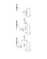
次に、実施形態1に係る検出動作の具体例について説明する。図36は、実施形態1に係る検出動作の手順を示すフローチャートである。図37は、ホバー検出期間における表示装置の動作例を示すタイミング波形図である。 図38は、実施形態1に係るホバー検出の閾値の一例を示す図である。図38の横軸は、駆動電極CDを示す。図38の縦軸は、信号強度を示す。信号強度は、駆動電極CDから出力される検出信号Vdet2の差分(絶対値|ΔVB|)である。図38の縦軸のCL1が、駆動電極CDを検出電極とするホバー検出の閾値である。図38の縦軸のCLAは、相互静電容量方式によるタッチ検出を行う必要があるかどうかを判断するための閾値である。閾値CLAの値は、閾値CL1の値と同じ又は閾値CL1よりも大きい(CLA≧CL1)。図39は、ホバー検出による被検出体の検出位置の一例を示す図である。図38及び図39は、複数の駆動電極CD1からCD16のうち、駆動電極CD10から出力される検出信号Vdet2の差分|ΔVB|が、閾値CL1以上で、かつ、閾値CLA以上ある場合を例示している。図40は、ホバー検出及びタッチ検出における表示装置と被検出体との関係を模式的に示す説明図である。 Next, a specific example of the detection operation according to the first embodiment will be described. FIG. 36 is a flowchart illustrating the procedure of the detection operation according to the first embodiment. FIG. 37 is a timing waveform diagram illustrating an operation example of the display device during the hover detection period. FIG. 38 is a diagram illustrating an example of a threshold for hover detection according to the first embodiment. The horizontal axis of FIG. 38 shows the drive electrode CD. The vertical axis | shaft of FIG. 38 shows signal strength. The signal intensity is a difference (absolute value | ΔVB |) of the detection signal Vdet2 output from the drive electrode CD. The vertical axis CL1 in FIG. 38 is a hover detection threshold value using the drive electrode CD as a detection electrode. The CLA on the vertical axis in FIG. 38 is a threshold value for determining whether or not it is necessary to perform touch detection by the mutual capacitance method. The value of the threshold value CLA is the same as or larger than the threshold value CL1 (CLA ≧ CL1). FIG. 39 is a diagram illustrating an example of the detection position of the detection target by hover detection. FIG. 38 and FIG. 39 exemplify a case where the difference | ΔVB | of the detection signal Vdet2 output from the drive electrode CD10 among the plurality of drive electrodes CD1 to CD16 is greater than or equal to the threshold value CL1 and greater than or equal to the threshold value CLA. Yes. FIG. 40 is an explanatory diagram schematically illustrating the relationship between the display device and the detection target in hover detection and touch detection.
本実施形態では、図17に示した検出動作期間Pt1及びPt2は、自己静電容量方式によるホバー検出期間と、相互静電容量方式によるタッチ検出期間とをそれぞれ含む。図36に示すステップST1は表示動作期間Pd1又はPd2に対応し、ステップST2、ST3は検出動作期間Pt1又はPt2におけるホバー検出期間に対応し、ステップST4は検出動作期間Pt1又はPt2におけるタッチ検出期間に対応している。 In the present embodiment, the detection operation periods Pt1 and Pt2 illustrated in FIG. 17 include a hover detection period based on the self-capacitance method and a touch detection period based on the mutual capacitance method. Step ST1 shown in FIG. 36 corresponds to the display operation period Pd1 or Pd2, steps ST2 and ST3 correspond to the hover detection period in the detection operation period Pt1 or Pt2, and step ST4 corresponds to the touch detection period in the detection operation period Pt1 or Pt2. It corresponds.
図36のステップST1では、制御部11(図1参照)が、ゲートドライバ12(図1参照)、ソースドライバ13(図1参照)及び駆動電極ドライバ14(図1参照)を介して、表示部20(図1参照)に表示データの書き込みを行う。具体的には、制御部11は、接続切替回路17(図21参照)に制御信号を送信して、複数の駆動電極CDを表示用IC19に接続する。この状態で、駆動電極ドライバ14は、複数の駆動電極CDに表示用の共通電極電位である表示用の駆動信号Vcomdcをそれぞれ供給する。これにより、複数の駆動電極CDの電位は、表示用の駆動信号Vcomdcに固定される。この状態で、ゲートドライバ12はゲート線GCLに制御信号を順次出力し、ソースドライバ13はデータ線SGLに画素信号Vpixを順次出力する。このようにして、制御部11は、表示動作期間Pd1に選択される複数行の画素Pix(図14参照)に画素信号Vpixを順次供給して、表示データの書き込みを行う。 In step ST1 of FIG. 36, the control unit 11 (see FIG. 1) displays the display unit via the gate driver 12 (see FIG. 1), the source driver 13 (see FIG. 1), and the drive electrode driver 14 (see FIG. 1). Display data is written to 20 (see FIG. 1). Specifically, the
次に、図36のステップST2では、駆動電極ドライバ14及び検出部40(図1参照)が、ホバー検出を行う。ホバー検出は、駆動電極CDを検出電極とする自己静電容量方式で行われる。具体的には、制御部11は、接続切替回路17に制御信号を送信して、複数の駆動電極CDを検出用IC75に接続する。この状態で、駆動電極ドライバ14は、配線27を介して、複数の駆動電極CDの各々に検出用の駆動信号Vcomを供給する。例えば図37に示すように、駆動電極ドライバ14は、駆動電極CD1からCD16に、検出用の駆動信号Vcomを同じ波形で且つ同期して供給する。これにより、駆動電極CD1からCD16から、静電容量変化に基づく検出信号Vdet2が同時に出力される。 Next, in step ST2 of FIG. 36, the drive electrode driver 14 and the detection unit 40 (see FIG. 1) perform hover detection. The hover detection is performed by a self-capacitance method using the drive electrode CD as a detection electrode. Specifically, the
検出部40は、複数の駆動電極CDから出力される検出信号Vdet2をそれぞれ取得する。そして、検出部40は、取得した検出信号Vdet2に基づく演算処理を行い、演算処理の結果から、ホバー検出における被検出体の有無を判断する。また、検出部40は、ホバー検出において被検出体が有ると判断される場合は、被検出体の位置を特定する。 The
例えば、ステップST2において、複数の駆動電極CD(CD1からCD16)からそれぞれ出力される検出信号Vdet2の差分|ΔVB|が、図38に示す閾値CL1とそれぞれ比較される。この比較は、例えば、検出部40の信号処理部44(図2参照)が行う。複数の駆動電極CD(CD1からCD16)からそれぞれ出力される検出信号Vdet2の1つ以上について、検出信号Vdet2の差分|ΔVB|が閾値CL1以上であれば、信号処理部44は、ホバー検出において被検出体が検出されたと判断する。その場合、検出部40の座標抽出部45(図2参照)は、閾値CL1以上の差分|ΔVB|を出力した駆動電極CDの位置を、被検出体の位置として検出する。図38及び図39に示す例では、信号処理部44は、駆動電極CD10において、被検出体が検出されたと判断する。座標抽出部45は、表示パネル10における駆動電極CD10の位置を、ホバー検出における被検出体の位置として検出する。一方、複数の駆動電極CDから出力される各検出信号Vdet2の差分|ΔVB|が全て閾値CL1未満であれば、信号処理部44は、ホバー検出において被検出体は検出されないと判断する。 For example, in step ST2, the difference | ΔVB | of the detection signals Vdet2 respectively output from the plurality of drive electrodes CD (CD1 to CD16) is compared with the threshold value CL1 shown in FIG. This comparison is performed, for example, by the signal processing unit 44 (see FIG. 2) of the
ホバー検出において被検出体CQが検出されない場合、図40に示すように、被検出体CQは表示装置1の表示面1aに対して非存在状態にある。被検出体CQと表示面1aとは距離D11離れて配置されている。また、被検出体CQと駆動電極CDとの間には静電容量C2aが形成されている。一方、ホバー検出において被検出体CQが検出される場合、被検出体CQは表示装置1の表示面1aに対して非接触状態又は接触状態にある。非接触状態では、被検出体CQと表示面1aとは距離D12離れて配置されている。距離D12は、距離D11よりも短い値である。また、被検出体CQと駆動電極CDとの間には静電容量C2bが形成されている。容量C2bは、容量C2aよりも大きい値である。 When the detection target CQ is not detected in the hover detection, the detection target CQ is not present with respect to the display surface 1a of the
なお、駆動電極ドライバ14は、ホバー検出の際に、検出用の駆動信号Vcomと同じ波形で、かつ駆動信号Vcomに同期したガード信号Vgd(図37参照)をタッチ検出電極TD1からTD16に供給する。または、駆動電極ドライバ14は、タッチ検出電極TD1からTD16を、電気的にどことも接続されていない状態(Hi−Z;図37参照)としてもよい。これによれば、タッチ検出電極TDと、検出用の駆動信号Vcomが供給される駆動電極CDとの間に静電容量が生じることを防ぐことができるので、ホバー検出の感度を高めることができる。 The drive electrode driver 14 supplies a guard signal Vgd (see FIG. 37) having the same waveform as that of the detection drive signal Vcom and synchronized with the drive signal Vcom to the touch detection electrodes TD1 to TD16 during hover detection. . Alternatively, the drive electrode driver 14 may be in a state where the touch detection electrodes TD1 to TD16 are not electrically connected anywhere (Hi-Z; see FIG. 37). According to this, since it is possible to prevent a capacitance from being generated between the touch detection electrode TD and the drive electrode CD to which the detection drive signal Vcom is supplied, the sensitivity of hover detection can be increased. .
次に、図36のステップST3では、検出部40は、ホバー検出(ステップST2)で取得した検出信号Vdet2に基づいて、相互静電容量方式によるタッチ検出を行う必要があるかどうかを判断する。つまり、検出部40は、相互静電容量方式によるタッチ検出を行った場合に被検出体を検出できるかどうかを、ホバー検出の検出結果に基づいて予測する。そして、検出部40は、タッチ検出で被検出体を検出できると予測される場合に、タッチ検出を行う。 Next, in step ST3 of FIG. 36, the
具体的には、検出部40の信号処理部44(図2参照)は、複数の駆動電極CD(CD1からCD16)の各々について、検出信号Vdet2の差分|ΔVB|を閾値CLAと比較する。そして、複数の駆動電極CDからそれぞれ出力される検出信号Vdet2の1つ以上について、検出信号Vdet2の差分|ΔVB|が閾値CLA以上であれば、信号処理部44は、相互静電容量方式によるタッチ検出を行う必要があると判断する。図38及び図39に示す例では、駆動電極ブロックCD10において被検出体が閾値CLA以上の強度で検出されているため、信号処理部44は、相互静電容量方式によるタッチ検出を行う必要があると判断する。一方、複数の駆動電極CDから出力される各検出信号Vdet2の差分|ΔVB|が全て閾値CLA未満であれば、信号処理部44は、相互静電容量方式によるタッチ検出を行う必要はないと判断する。 Specifically, the signal processing unit 44 (see FIG. 2) of the
信号処理部44が相互静電容量方式によるタッチ検出を行う必要があると判断する場合(ステップST3;Yes)は、図36のステップST4へ進む。また、信号処理部44が相互静電容量方式によるタッチ検出を行う必要はないと判断する場合(ステップST3;No)は、ステップST1へ戻る。このように、信号処理部44は、ステップST3において、相互静電容量方式によるタッチ検出(ステップST4)の要、不要を予め判断する。これにより、タッチ検出が不要と判断されるときは、検出部40は、ステップST4の検出動作を省くことができ、タッチ検出に要する電力使用量を削減することができる。また、検出部40は、ステップST4を省いた分だけ、ホバー検出(ステップST2)の実行回数を増やすことができる。 When the
図36のステップST4では、駆動電極ドライバ14及び検出部40が、タッチ検出を行う。タッチ検出は、タッチ検出電極TDを検出電極とする相互静電容量方式で行われる。具体的には、制御部11は、接続切替回路17に制御信号を送信して、複数の駆動電極CDを検出用IC75に接続する。この状態で、駆動電極ドライバ14は、配線27を介して複数の駆動電極CDに検出用の駆動信号Vcomを供給する。 In step ST4 of FIG. 36, the drive electrode driver 14 and the
図41は、タッチ検出期間における表示装置の動作例を示すタイミング波形図である。図42は、実施形態1に係るタッチ検出の閾値の一例を示す図である。図42の横軸は、駆動電極CD10と平面視で重なるタッチ検出電極TDを示す。図42の縦軸は、信号強度を示す。信号強度は、タッチ検出電極TDから出力される検出信号Vdet1の差分(絶対値|ΔVA|)である。図43は、タッチ検出による被検出体の検出位置の一例を示す図である。図41に示すように、駆動電極ドライバ14は、駆動電極CD1からCD16に、検出用の駆動信号Vcomを同じ波形で且つそれぞれ異なるタイミングで供給する。駆動電極CD1からCD16間で、駆動信号Vcomが供給される順番に特に制限はないが、一例を挙げると、駆動電極CD1、CD2、CD3、…CD16の順である。これにより、駆動電極CDとタッチ検出電極TDとの間の静電容量変化に基づいて、タッチ検出電極TDから検出信号Vdet1が出力される。例えば、駆動電極CD1に駆動信号Vcomが供給されている間、駆動電極CD1と対向する位置に配置されたタッチ検出電極TD1からTD16から、駆動電極CDとの間の静電容量変化に基づいて検出信号Vdet1がそれぞれ出力される。 FIG. 41 is a timing waveform diagram illustrating an operation example of the display device in the touch detection period. FIG. 42 is a diagram illustrating an example of a threshold value for touch detection according to the first embodiment. The horizontal axis in FIG. 42 indicates the touch detection electrode TD that overlaps the drive electrode CD10 in plan view. The vertical axis in FIG. 42 indicates the signal intensity. The signal intensity is a difference (absolute value | ΔVA |) of the detection signal Vdet1 output from the touch detection electrode TD. FIG. 43 is a diagram illustrating an example of the detection position of the detection target by touch detection. As shown in FIG. 41, the drive electrode driver 14 supplies the drive signals Vcom for detection to the drive electrodes CD1 to CD16 with the same waveform and at different timings. There is no particular restriction on the order in which the drive signal Vcom is supplied between the drive electrodes CD1 to CD16. However, for example, the order is the drive electrodes CD1, CD2, CD3,... CD16. Accordingly, the detection signal Vdet1 is output from the touch detection electrode TD based on the change in electrostatic capacitance between the drive electrode CD and the touch detection electrode TD. For example, while the drive signal Vcom is supplied to the drive electrode CD1, detection is performed from the touch detection electrodes TD1 to TD16 arranged at positions facing the drive electrode CD1 based on the capacitance change between the drive electrode CD. A signal Vdet1 is output.
検出部40は、複数のタッチ検出電極TDからそれぞれ出力される検出信号Vdet1を取得する。そして、検出部40は、取得した検出信号Vdet1に基づく演算処理を行い、演算処理の結果から、タッチ検出における被検出体の有無を判断する 。また、検出部40は、タッチ検出において被検出体が有ると判断される場合は、被検出体の位置を特定する。 The
例えば、ステップST4において、複数のタッチ検出電極TD(TD1からTD16)からそれぞれ出力される検出信号Vdet1の差分|ΔVA|が、図42に示す閾値CL2とそれぞれ比較される。この比較は、例えば、検出部40の信号処理部44(図2参照)が行う。複数のタッチ検出電極TD(TD1からTD16)からそれぞれ出力される検出信号Vdet1の1つ以上について、検出信号Vdet1の差分|ΔVA|が閾値CL2以上であれば、信号処理部44は、タッチ検出において被検出体が検出されたと判断する。その場合、検出部40の座標抽出部45(図2参照)は、閾値CL2以上の差分|ΔVA|を出力したタッチ検出電極TDの位置を、被検出体の位置として検出する。図42及び図43に示す例では、信号処理部44は、駆動電極CD10と平面視で重なるタッチ検出電極TD6、TD7、TD10及びTD11において、被検出体が検出されたと判断する。座標抽出部45は、表示パネル10において、駆動電極CD10と平面視で重なるタッチ検出電極TD6、TD7、TD10及びTD11の位置を、タッチ検出における被検出体の位置として検出する。一方、複数のタッチ検出電極TDから出力される各検出信号Vdet1の差分|ΔVA|が全て閾値CL1未満であれば、信号処理部44は、タッチ検出において被検出体は検出されないと判断する。 For example, in step ST4, the difference | ΔVA | of the detection signals Vdet1 respectively output from the plurality of touch detection electrodes TD (TD1 to TD16) is compared with the threshold value CL2 shown in FIG. This comparison is performed, for example, by the signal processing unit 44 (see FIG. 2) of the
図43に示すように、タッチ検出電極TDは、駆動電極CDよりも平面視によるサイズが小さく、且つ個数が多い。このため、タッチ検出電極TDによるタッチ検出は、駆動電極CDによるホバー検出よりも、検出位置の精度が高い。 As shown in FIG. 43, the touch detection electrode TD has a smaller size and a larger number in plan view than the drive electrode CD. For this reason, the touch detection by the touch detection electrode TD has higher detection position accuracy than the hover detection by the drive electrode CD.
タッチ検出において被検出体CQが検出されたと判断される場合、図40に示すように、被検出体CQは、表示装置1の表示面1aに対して接触状態にある。被検出体CQと駆動電極CD(図示しない)との間に形成される静電容量は、上述の静電容量C2a、C2bの各値よりも大きい値である。ステップST4の後は、ステップST1に戻り、表示動作期間Pd2となる。また、表示動作期間Pd2の後に、検出動作期間Pt2が続く。 When it is determined that the detection target CQ is detected in the touch detection, the detection target CQ is in contact with the display surface 1a of the
なお、図17において、1フレーム期間の検出動作期間Pt1でホバー検出又はタッチ検出により被検出体が検出された場合、その検出結果を反映した表示データが、例えば次の1フレーム期間の表示動作期間Pd2で、表示部20に書き込まれる。同様に、1フレーム期間の検出動作期間Pt2でホバー検出又はタッチ検出により被検出体が検出された場合、その検出結果を反映した表示データが、例えば次の1フレーム期間の表示動作期間Pd1で表示部20に書き込まれる。 In FIG. 17, when a detection target is detected by hover detection or touch detection in the detection operation period Pt1 of one frame period, the display data reflecting the detection result is, for example, the display operation period of the next one frame period. It is written in the
以上説明したように、本発明の実施形態1に係る表示装置1は、行方向と列方向とにそれぞれ並ぶ複数の駆動電極CDと、行方向と列方向とにそれぞれ並ぶ複数のタッチ検出電極TDと、を有する。複数の駆動電極CDそれぞれは、複数のタッチ検出電極TDと平面視で重なる。これによれば、タッチ検出の際に、駆動電極ドライバ14は複数の駆動電極CDに駆動信号Vcomを順次供給し、検出部40はタッチ検出電極TDから出力される検出信号Vdet1に基づいてタッチ入力を検出する。これにより、タッチ検出電極TDの配列に応じた検出精度でタッチ検出を実行できる。一方、ホバー検出において、駆動電極ドライバ14は、複数の駆動電極CDに駆動信号Vcomを同時に供給する。検出部40は、複数の駆動電極CDからそれぞれ出力された検出信号Vdet2に基づいて、ホバー検出を行う。 As described above, the
表示装置1では、1つの駆動電極CDと重なる位置に複数のタッチ検出電極TDが配置されている。1個の駆動電極CDは、1個のタッチ検出電極TDよりも平面視による大きさが大きい。例えば、駆動電極CDの平面視による形状は四角形であり、四角形の1辺の長さは20mm以上30mm以下である。また、タッチ検出電極TDの平面視による形状は四角形であり、四角形の1辺の長さは4mm以上5mm以下である。これにより、タッチ検出電極TDから発生する電界の電気力線よりも、検出電極CDから発生する電界の電気力線の方が、表示面からより離れた位置まで到達する。したがって、表示装置1は、ホバー検出における検出感度を高めることができ、非接触状態における被検出体を良好に検出することができる。これにより、表示装置1は、タッチ検出とホバー検出とを良好に行うことができる 。なお、本実施形態では、表示装置1において、タッチ検出電極TDの個数は駆動電極CDの個数よりも多い。一例を挙げると、図25及び図26に示したように、1個の駆動電極CDと平面視で重なる位置に16個のタッチ検出電極TDが配置されており、タッチ検出電極TDの個数は駆動電極CDの個数の16倍となっている。 In the
実施形態1では、行方向が本発明の「第1方向」に対応し、列方向が本発明の「第2方向」に対応している。また、駆動電極CDが本発明の「第1電極」に対応し、タッチ検出電極TDが本発明の「第2電極」に対応している。また、配線27が本発明の「第1配線」に対応し、配線37が本発明の「第2配線」に対応し、配線26が本発明の「第3配線」に対応している。また、フレキシブル基板71が本発明の「接続部」に対応している。また、検出信号Vdet1が本発明の「第1検出信号」に対応し、検出信号Vdet2が本発明の「第2検出信号」に対応している。また、駆動電極ドライバ14が本発明の「駆動回路」に対応している。また、第1基板2が本発明の「基板」に対応している。また、複数の駆動電極CDと、複数のタッチ検出電極TDとを備える装置が、本発明の「検出装置」に対応している。 In the first embodiment, the row direction corresponds to the “first direction” of the present invention, and the column direction corresponds to the “second direction” of the present invention. The drive electrode CD corresponds to the “first electrode” of the present invention, and the touch detection electrode TD corresponds to the “second electrode” of the present invention. The wiring 27 corresponds to the “first wiring” of the present invention, the
なお、実施形態1では、フレキシブル基板71を介して、タッチ検出電極TDが検出用IC75に接続されている場合について説明した。しかしながら、本発明の実施形態では、フレキシブル基板71を用いずに、タッチ検出電極TDと検出用IC75とが接続されていてもよい。 In the first embodiment, the case where the touch detection electrode TD is connected to the
(変形例1)
図44は、実施形態1に係る表示装置の変形例1を示す断面図である。図44に示すように、対向基板31の第1面31aは、TFT基板21の第1面21aよりも面積が小さく、対向基板31の端部とTFT基板21との間には段差部8が生じている。段差部8は、対向基板31の側面31cを含む。変形例1では、タッチ検出電極TDに接続する配線37は、例えば、対向基板31の第1面31aから側面31cまで設けられている。また、変形例1では、側面31cに導電体50が設けられている。導電体50は、液晶層6を封止するための封止材9を側方から覆うように設けられており、配線37と、TFT基板21上に設けられた配線26とを接続している。このような構成であっても、タッチ検出電極TDは、導電体50を介して検出用IC75に接続することができる。(Modification 1)
FIG. 44 is a cross-sectional view illustrating a first modification of the display device according to the first embodiment. As shown in FIG. 44, the
また、本発明の実施形態では、対向基板31に、表面31aと裏面31bとの間を貫く貫通電極が設けられていてもよい。また、貫通電極を介して、タッチ検出電極TDと検出用IC75とが接続されていてもよい。変形例1では、導電体50が本発明の「接続部」に対応している。 In the embodiment of the present invention, the
(変形例2)
図45は、実施形態1に係る表示装置の変形例2を示す断面図である。図45に示すように、対向基板31は、第1面31aと第2面31bとの間を貫通する貫通孔VHAを有する。貫通孔VHAは、対向基板31の第1面31aに設けられた配線37も貫通している。また、TFT基板21に設けられた配線26は、貫通孔VHAと対向する位置に貫通孔VHBを有する。(Modification 2)
FIG. 45 is a cross-sectional view illustrating a second modification of the display device according to the first embodiment. As shown in FIG. 45, the
また、TFT基板21は、貫通孔VHBと対向する位置に凹部CCを有する。凹部CCは、TFT基板21の第1面21a側に開口するとともに、第1面21aと第2面21bとの間に底部を有する。凹部CCの深さは、例えば、TFT基板21の厚さの1/5以上、1/2以下である。表示装置1の厚さ方向(Z方向)において、凹部CC、貫通孔VHB及び貫通孔VHAは、この順に並んでおり、Z方向に延設された接続用孔を構成している。なお、変形例2では、TFT基板21は、凹部CCの代わりに、第1面21aと第2面21bとの間を貫通する貫通孔を有していてもよい。 The
貫通電極TGVは、貫通孔VHAを通って配線26及び配線37を電気的に接続している。図45に示す例では、貫通電極TGVは、配線37の上面37a、貫通孔VHAにおける配線37の内面37s、及び、貫通孔VHAにおける対向基板31の内面31sにそれぞれ接触している。内面37s、31sは、貫通孔VHAの内面を形成している。また、貫通電極TGVは、貫通孔VHBにおける配線26の内面26s及び凹部CCの内面にもそれぞれ接触している。内面26sは、貫通孔VHBの内面を形成している。 The through electrode TGV electrically connects the
なお、図45に示す例では、貫通電極TGVは、貫通孔VHA、VB及び凹部CCに充填されているが、貫通電極TGVは、貫通孔VHA、VB及び凹部CCの内面に接し、配線26と配線37との間を途切れることなく連続的に設けられていればよい。貫通電極TGVは、例えば、銀などの金属材料を含み、金属材料の粒径が数ナノメートルから数十ナノメートルのオーダーの微粒子を含むものであることが望ましい。このような構成であっても、タッチ検出電極TDは、貫通電極TGVを介して検出用IC75に接続することができる。 In the example shown in FIG. 45, the through electrode TGV is filled in the through holes VHA, VB and the recess CC, but the through electrode TGV is in contact with the inner surfaces of the through holes VHA, VB, and the recess CC, and What is necessary is just to provide continuously without interrupting between the
また、変形例2においても、TFT基板21の端部と対向基板31との間に、液晶層を封止するための封止材や、TFT基板21と対向基板31とを接着するための接着層が配置されていてもよい。TFT基板21の端部と対向基板31との間に封止材や接着層が存在する場合、貫通電極TGVの側面は封止材又は接着層と接していてもよい。変形例2では、貫通電極TGVが本発明の「接続部」に対応している。 Also in the modified example 2, a sealing material for sealing the liquid crystal layer between the end of the
(実施形態2)
実施形態1では、駆動電極CDと、駆動電極CDに接続する配線27とが同一の層に設けられている場合について説明した。しかしながら、本実施形態では、駆動電極CDと、駆動電極CDに接続する配線は、互いに異なる層に設けられていてもよい。(Embodiment 2)
In the first embodiment, the case where the drive electrode CD and the wiring 27 connected to the drive electrode CD are provided in the same layer has been described. However, in the present embodiment, the drive electrode CD and the wiring connected to the drive electrode CD may be provided in different layers.
図46は、実施形態2に係る第1基板を模式的に示す平面図である。また、図47は、図46の一部をA5−A6線で切断して拡大した断面図である。図46に示すように、実施形態2に係る第1基板2Aは、列方向に延設された複数の配線53を有する。複数の配線53は複数の駆動電極CDにそれぞれ1本ずつ接続している。複数の駆動電極CDの各々は配線53を介して接続切替回路17に接続している。 FIG. 46 is a plan view schematically showing the first substrate according to the second embodiment. FIG. 47 is an enlarged cross-sectional view of a part of FIG. 46 taken along line A5-A6. As illustrated in FIG. 46, the
図47に示すように、実施形態2に係る第1基板2Aは、画素電極22と駆動電極CDとを絶縁する絶縁層24として、第1絶縁層241と第2絶縁層242とを有する。第1絶縁層241には、駆動電極CDに至る貫通穴H21が設けられている。配線53は第1絶縁層241上に設けられており、貫通穴H21を介して駆動電極CDに接続している。また、配線53は第2絶縁層242で覆われている。画素電極22は、第2絶縁層242上に設けられている。このような構成であっても、複数の駆動電極CDの各々は、配線53を介して、表示用IC19(図21参照)や検出用IC75(図21参照)に接続することができる。したがって、実施形態2に係る第1基板2Aを有する表示装置は、実施形態1で説明した表示装置1と同様に、タッチ検出とホバー検出とを良好に行うことができる。なお、実施形態2では、第1基板2Aが本発明の「基板」に対応している。 As shown in FIG. 47, the
(実施形態3)
実施形態1では、タッチ検出電極TDと、タッチ検出電極TDに接続する配線37とが同一の層に設けられている場合について説明した。しかしながら、本実施形態では、タッチ検出電極TDと、タッチ検出電極TDに接続する配線は、互いに異なる層に設けられていてもよい。(Embodiment 3)
In the first embodiment, the case where the touch detection electrode TD and the
図48は、実施形態3に係る第2基板を模式的に示す平面図である。また、図49は、図48の一部をA7−A8線で切断して拡大した断面図である。図48に示すように、実施形態3に係る第2基板3Aは、列方向に延設された複数の配線153を有する。複数の配線153は複数のタッチ検出電極TDにそれぞれ1本ずつ接続している。 FIG. 48 is a plan view schematically showing the second substrate according to the third embodiment. FIG. 49 is an enlarged cross-sectional view of a part of FIG. 48 taken along line A7-A8. As shown in FIG. 48, the
複数のタッチ検出電極TDの各々は配線153を介して、例えばフレキシブル基板71の配線77に接続している。図49に示すように、実施形態3に係る第2基板3Aは、タッチ検出電極TDを覆う第1絶縁層251と、第1絶縁層251上に設けられた第2絶縁層252とを有する。第1絶縁層251には、タッチ検出電極TDに至る貫通穴H31が設けられている。配線153は第1絶縁層251上に設けられており、貫通穴H31を介してタッチ検出電極TDに接続している。また、配線153は第2絶縁層252で覆われている。偏光板35Aは、第2絶縁層252上に設けられている。このような構成であっても、複数のタッチ検出電極TDの各々は、配線153及びフレキシブル基板71を介して、検出用IC75(図21参照)に接続することができる。したがって、実施形態3に係る第2基板3Aを有する表示装置は、実施形態1で説明した表示装置1と同様に、タッチ検出とホバー検出とを良好に行うことができる。 Each of the plurality of touch detection electrodes TD is connected to, for example, the wiring 77 of the
(実施形態4)
上記の実施形態1では、表示パネル10は、表示部20に静電容量型のタッチセンサ30を内蔵して一体化した、いわゆるインセルタイプあるいはハイブリッドタイプの装置であることについて説明した。しかしながら、本実施形態において、表示パネル10は、表示部20の上にタッチセンサ30を装着した、いわゆるオンセルタイプの装置であってもよい。オンセルタイプの装置の場合、表示部20の直上にタッチセンサ30が設けられていてもよいし、表示部20の直上ではなく他の層を介して上方にタッチセンサ30が設けられていてもよい。(Embodiment 4)
In the first embodiment, it has been described that the
図50は、実施形態4に係るオンセルタイプの表示パネルの構成例を示す断面図である。図50に示すように、実施形態4に係るオンセルタイプの表示パネル10Aは、第1基板2Bと、第1基板2Bの表面に垂直な方向に対向して配置された第2基板3Bと、第1基板2Bと第2基板3Bとの間に配置された液晶層6と、第2基板3Bの液晶層6と向かい合う面の反対側に配置された検出装置4と、を備える。 FIG. 50 is a cross-sectional view illustrating a configuration example of an on-cell type display panel according to the fourth embodiment. As shown in FIG. 50, an on-cell
第1基板2Bは、TFT基板21と、TFT基板21の第1面21aに設けられた共通電極COMと、第1面21a上に設けられて共通電極COMを覆う絶縁層24と、絶縁層24上に設けられた画素電極22と、TFT基板21の第2面21bに設けられた偏光板35Bと、を有する。表示動作期間Pd1、Pd2(図17参照)では、共通電極COMに表示用の駆動信号Vcomdcが供給される。第2基板3Bは、対向基板31と、対向基板31の第1面31aに設けられた偏光板35Aと、対向基板31の第2面31bに設けられたカラーフィルタ32とを有する。 The
検出装置4は、例えば、偏光板35A上に設けられた複数の駆動電極CDと、偏光板35A上に設けられて複数の駆動電極CDを覆おう絶縁層25と、絶縁層25上に設けられた複数のタッチ検出電極TDと、絶縁層25上に設けられて複数のタッチ検出電極TDを覆うカバーガラス81とを有する。また、検出装置4は、複数のタッチ検出電極TDに接続する配線(図示せず)と、複数の駆動電極CDに接続する配線(図示せず)とを有する。このような構成であっても、複数の駆動電極CDの各々と、複数のタッチ検出電極TDの各々は、配線を介して検出用IC75(図18参照)に接続することができる。したがって、実施形態3に係る検出装置4は、実施形態1で説明した表示装置1と同様に、タッチ検出とホバー検出とを良好に行うことができる。 The detection device 4 is provided on the insulating
なお、実施形態4では、検出動作期間Pt1、Pt2において、共通電極COMに、検出用の駆動信号Vcomと同じ波形で、かつ駆動信号Vcomに同期したガード信号Vgdが供給されてもよい。または、検出動作期間Pt1、Pt2において、共通電極COMは、電気的にどことも接続されていない状態に設定されてもよい。これによれば、検出動作期間Pt1、Pt2において、共通電極COMと、検出用の駆動信号Vcomが供給される駆動電極CDとの間に静電容量が生じることを防ぐことができるので、検出の感度を高めることができる。実施形態4では、第1基板2Bが本発明の「第3基板」に対応している。 In the fourth embodiment, in the detection operation periods Pt1 and Pt2, a guard signal Vgd having the same waveform as the detection drive signal Vcom and synchronized with the drive signal Vcom may be supplied to the common electrode COM. Alternatively, in the detection operation periods Pt1 and Pt2, the common electrode COM may be set in a state where it is not electrically connected anywhere. According to this, in the detection operation periods Pt1 and Pt2, it is possible to prevent a capacitance from being generated between the common electrode COM and the drive electrode CD to which the detection drive signal Vcom is supplied. Sensitivity can be increased. In the fourth embodiment, the
以上、本発明の好適な実施の形態を説明したが、本発明はこのような実施の形態に限定されるものではない。実施の形態で開示された内容はあくまで一例にすぎず、本発明の趣旨を逸脱しない範囲で種々の変更が可能である。例えば、実施形態1では、カラー表示可能な液晶表示装置を示したが、本発明はカラー表示対応の液晶表示装置に限定されず、モノクロ表示対応の液晶表示装置であってもよい。本発明の趣旨を逸脱しない範囲で行われた適宜の変更についても、当然に本発明の技術的範囲に属する。 The preferred embodiment of the present invention has been described above, but the present invention is not limited to such an embodiment. The content disclosed in the embodiment is merely an example, and various modifications can be made without departing from the spirit of the present invention. For example, in the first embodiment, a liquid crystal display device capable of color display is shown, but the present invention is not limited to a liquid crystal display device compatible with color display, and may be a liquid crystal display device compatible with monochrome display. Appropriate changes made without departing from the spirit of the present invention naturally belong to the technical scope of the present invention.
例えば、本態様の検出装置及び表示装置は、以下の態様をとることができる。
(1)第1方向と、前記第1方向と交差する第2方向とにそれぞれ並ぶ複数の第1電極と、前記第1方向と前記第2方向とにそれぞれ並ぶ複数の第2電極と、を有し、前記複数の第1電極それぞれは、前記複数の第2電極と平面視で重なる、検出装置。
(2)前記複数の第1電極それぞれの平面視による大きさは、前記複数の第2電極それぞれの大きさより大きい、上記(1)に記載の検出装置。
(3)前記第1電極に接続する第1配線と、前記第1電極及び前記第1配線が設けられた第1基板と、前記第2電極に接続する第2配線と、前記第2電極及び前記第2配線が設けられた第2基板と、をさらに備え、1本の前記第2配線は、異なる前記第1電極と平面視で重なる複数の第2電極を、前記第2方向で接続する、上記(1)又は上記(2)に記載の検出装置。
(4)1本の前記第2配線は、異なる前記第1電極間であって、前記第1電極に対する位置が互いに同じである前記第2電極同士を接続する、上記(3)に記載の検出装置。
(5)前記第1電極及び前記第1配線は、前記第1基板上の同一の層に設けられている、上記(3)又は上記(4)に記載の検出装置。
(6)前記第2電極及び前記第2配線は、前記第2基板上の同一の層に設けられている、上記(3)乃至上記(5)のいずれか1項に記載の検出装置。
(7)前記第1電極と前記第2電極との間の容量変化に応じて前記第2電極から出力される第1検出信号、又は、前記第1電極の容量変化に応じて前記第1電極から出力される第2検出信号を検出する検出部、をさらに備える上記(1)乃至上記(6)のいずれか1項に記載の検出装置。
(8)前記第1電極に駆動信号を供給する駆動回路、をさらに備え、前記検出部が前記第2検出信号を検出する期間において、前記駆動回路は、前記駆動信号と同じ波形で、かつ前記駆動信号と同期したガード信号を、前記第2電極に供給する、上記(7)に記載の検出装置。
(9)前記検出部が前記第2検出信号を検出する期間において、前記第2電極は電気的にフローティング状態である、上記(7)又は上記(8)に記載の検出装置。
(10)上記(1)乃至上記(9)のいずれか1項に記載の検出装置と、前記検出装置と向かい合う第3基板と、前記検出装置と前記第3基板との間に配置された表示機能層と、を備える表示装置。
(11)第1方向と、前記第1方向と交差する第2方向とにそれぞれ並ぶ複数の第1電極と、前記複数の第1電極が設けられた第1基板と、前記第1方向と前記第2方向とにそれぞれ並ぶ複数の第2電極と、前記複数の第2電極が設けられた第2基板と、前記第1基板と前記第2基板との間に設けられた表示機能層と、を有し、前記複数の第1電極それぞれは、前記複数の第2電極と平面視で重なり、前記複数の第1電極それぞれの平面視による大きさは、前記複数の第2電極それぞれの大きさより大きい、表示装置。
(12)前記第1電極と前記第2電極との間の容量変化に応じて前記第2電極から出力される第1検出信号、又は、前記第1電極の容量変化に応じて前記第1電極から出力される第2検出信号を検出する検出部、をさらに備える上記(11)に記載の表示装置。
(13)前記第1電極に接続する第1配線と、前記第1電極及び前記第1配線が設けられた第1基板と、前記第2電極に接続する第2配線と、前記第2電極及び前記第2配線が設けられた第2基板と、前記第1基板に設けられた第3配線と、前記第2配線と前記第3配線とを接続する接続部と、をさらに備え、前記第1基板は、画像を表示する表示領域と、前記表示領域の周囲に位置する額縁領域とを有し、前記第3配線は前記額縁領域に設けられている、上記(10)乃至上記(12)のいずれか1項に記載の表示装置。
(14)複数本の前記第2配線が、前記接続部を介して、1本の前記第3配線に接続している、上記(13)に記載の表示装置。For example, the detection device and display device of this aspect can take the following aspects.
(1) A plurality of first electrodes arranged in a first direction and a second direction intersecting the first direction, and a plurality of second electrodes arranged in the first direction and the second direction, respectively. Each of the plurality of first electrodes overlaps the plurality of second electrodes in plan view.
(2) The detection device according to (1), wherein a size of each of the plurality of first electrodes in plan view is larger than a size of each of the plurality of second electrodes.
(3) a first wiring connected to the first electrode, a first substrate provided with the first electrode and the first wiring, a second wiring connected to the second electrode, the second electrode, A second substrate on which the second wiring is provided, wherein one second wiring connects a plurality of second electrodes overlapping the different first electrodes in plan view in the second direction. The detection device according to (1) or (2) above.
(4) The detection according to (3), wherein the one second wiring connects the second electrodes that are between the different first electrodes and are at the same position with respect to the first electrodes. apparatus.
(5) The detection device according to (3) or (4), wherein the first electrode and the first wiring are provided in the same layer on the first substrate.
(6) The detection device according to any one of (3) to (5), wherein the second electrode and the second wiring are provided in the same layer on the second substrate.
(7) The first detection signal output from the second electrode according to a change in capacitance between the first electrode and the second electrode, or the first electrode according to a change in capacitance of the first electrode The detection device according to any one of (1) to (6), further including a detection unit that detects a second detection signal output from the first detection signal.
(8) a drive circuit for supplying a drive signal to the first electrode, and in a period in which the detection unit detects the second detection signal, the drive circuit has the same waveform as the drive signal, and The detection device according to (7), wherein a guard signal synchronized with a drive signal is supplied to the second electrode.
(9) The detection device according to (7) or (8), wherein the second electrode is in an electrically floating state during a period in which the detection unit detects the second detection signal.
(10) The detection device according to any one of (1) to (9) above, a third substrate facing the detection device, and a display disposed between the detection device and the third substrate And a functional layer.
(11) A plurality of first electrodes arranged in a first direction and a second direction intersecting the first direction, a first substrate provided with the plurality of first electrodes, the first direction, and the first direction A plurality of second electrodes respectively arranged in a second direction, a second substrate provided with the plurality of second electrodes, a display function layer provided between the first substrate and the second substrate, Each of the plurality of first electrodes overlaps with the plurality of second electrodes in a plan view, and each of the plurality of first electrodes in a plan view has a size larger than that of each of the plurality of second electrodes. Big display device.
(12) The first detection signal output from the second electrode according to a change in capacitance between the first electrode and the second electrode, or the first electrode according to a change in capacitance of the first electrode The display device according to (11), further including a detection unit configured to detect a second detection signal output from.
(13) a first wiring connected to the first electrode; a first substrate provided with the first electrode and the first wiring; a second wiring connected to the second electrode; the second electrode; A second substrate provided with the second wiring; a third wiring provided on the first substrate; and a connecting portion for connecting the second wiring and the third wiring. The substrate has a display area for displaying an image and a frame area located around the display area, and the third wiring is provided in the frame area. The display device according to any one of the above.
(14) The display device according to (13), wherein a plurality of the second wirings are connected to one third wiring through the connection portion.
1 表示装置
2、2A、2B 第1基板
3、3A、3B 第2基板
4 検出装置
10 表示パネル
10a 表示領域
10b 額縁領域
11 制御部
14 駆動電極ドライバ
17 接続切替回路
19 表示用IC
20 表示部
21 TFT基板
22 画素電極
30 タッチセンサ
31 対向基板
32 カラーフィルタ
40 検出部
42 検出信号増幅部
43 A/D変換部
44 信号処理部
45 座標抽出部
46 検出タイミング制御部
71、73 フレキシブル基板
75 検出用IC
CD 駆動電極
DET 電圧検出器
Pd1、Pd2 表示動作期間
Pt1、Pt2 検出動作期間
Sg 交流矩形波
TD タッチ検出電極
Vcom 駆動信号
Vdet1、Vdet2 検出信号
Vgd ガード信号DESCRIPTION OF
20
CD drive electrode DET voltage detector Pd1, Pd2 display operation period Pt1, Pt2 detection operation period Sg AC rectangular wave TD touch detection electrode Vcom drive signal Vdet1, Vdet2 detection signal Vgd guard signal
Claims (14)
Translated fromJapanese前記第1方向と前記第2方向とにそれぞれ並ぶ複数の第2電極と、
を有し、
前記複数の第1電極それぞれは、前記複数の第2電極と平面視で重なる、検出装置。A plurality of first electrodes respectively arranged in a first direction and a second direction intersecting the first direction;
A plurality of second electrodes respectively arranged in the first direction and the second direction;
Have
Each of the plurality of first electrodes overlaps the plurality of second electrodes in plan view.
前記第1電極及び前記第1配線が設けられた第1基板と、
前記第2電極に接続する第2配線と、
前記第2電極及び前記第2配線が設けられた第2基板と、をさらに備え、
1本の前記第2配線は、異なる前記第1電極と平面視で重なる複数の第2電極を、前記第2方向で接続する、請求項1又は請求項2に記載の検出装置。A first wiring connected to the first electrode;
A first substrate provided with the first electrode and the first wiring;
A second wiring connected to the second electrode;
A second substrate provided with the second electrode and the second wiring, and
3. The detection device according to claim 1, wherein one of the second wirings connects a plurality of second electrodes that overlap with the different first electrodes in plan view in the second direction.
異なる前記第1電極間であって、前記第1電極に対する位置が互いに同じである前記第2電極同士を接続する、請求項3に記載の検出装置。One second wiring is
The detection apparatus according to claim 3, wherein the second electrodes that are different between the first electrodes and that have the same position with respect to the first electrode are connected to each other.
前記検出部が前記第2検出信号を検出する期間において、前記駆動回路は、前記駆動信号と同じ波形で、かつ前記駆動信号と同期したガード信号を、前記第2電極に供給する、請求項7に記載の検出装置。A drive circuit for supplying a drive signal to the first electrode;
The period during which the detection unit detects the second detection signal, the drive circuit supplies a guard signal having the same waveform as the drive signal and synchronized with the drive signal to the second electrode. The detection device according to 1.
前記検出装置と向かい合う第3基板と、
前記検出装置と前記第3基板との間に配置された表示機能層と、を備える表示装置。The detection device according to any one of claims 1 to 9,
A third substrate facing the detection device;
And a display function layer disposed between the detection device and the third substrate.
前記複数の第1電極が設けられた第1基板と、
前記第1方向と前記第2方向とにそれぞれ並ぶ複数の第2電極と、
前記複数の第2電極が設けられた第2基板と、
前記第1基板と前記第2基板との間に設けられた表示機能層と、
を有し、
前記複数の第1電極それぞれは、前記複数の第2電極と平面視で重なり、
前記複数の第1電極それぞれの平面視による大きさは、前記複数の第2電極それぞれの大きさより大きい、表示装置。A plurality of first electrodes respectively arranged in a first direction and a second direction intersecting the first direction;
A first substrate provided with the plurality of first electrodes;
A plurality of second electrodes respectively arranged in the first direction and the second direction;
A second substrate provided with the plurality of second electrodes;
A display functional layer provided between the first substrate and the second substrate;
Have
Each of the plurality of first electrodes overlaps the plurality of second electrodes in plan view,
The size of each of the plurality of first electrodes in plan view is larger than the size of each of the plurality of second electrodes.
前記第1電極及び前記第1配線が設けられた第1基板と、
前記第2電極に接続する第2配線と、
前記第2電極及び前記第2配線が設けられた第2基板と、
前記第1基板に設けられた第3配線と、
前記第2配線と前記第3配線とを接続する接続部と、をさらに備え、
前記第1基板は、画像を表示する表示領域と、前記表示領域の周囲に位置する額縁領域とを有し、
前記第3配線は前記額縁領域に設けられている、請求項10乃至請求項12のいずれか1項に記載の表示装置。A first wiring connected to the first electrode;
A first substrate provided with the first electrode and the first wiring;
A second wiring connected to the second electrode;
A second substrate provided with the second electrode and the second wiring;
A third wiring provided on the first substrate;
A connecting portion for connecting the second wiring and the third wiring;
The first substrate has a display area for displaying an image, and a frame area located around the display area,
The display device according to claim 10, wherein the third wiring is provided in the frame region.
Priority Applications (2)
| Application Number | Priority Date | Filing Date | Title |
|---|---|---|---|
| JP2017131477AJP6857563B2 (en) | 2017-07-04 | 2017-07-04 | Detection device and display device |
| US16/024,981US10585540B2 (en) | 2017-07-04 | 2018-07-02 | Detection device and display device |
Applications Claiming Priority (1)
| Application Number | Priority Date | Filing Date | Title |
|---|---|---|---|
| JP2017131477AJP6857563B2 (en) | 2017-07-04 | 2017-07-04 | Detection device and display device |
Publications (2)
| Publication Number | Publication Date |
|---|---|
| JP2019016064Atrue JP2019016064A (en) | 2019-01-31 |
| JP6857563B2 JP6857563B2 (en) | 2021-04-14 |
Family
ID=64903195
Family Applications (1)
| Application Number | Title | Priority Date | Filing Date |
|---|---|---|---|
| JP2017131477AActiveJP6857563B2 (en) | 2017-07-04 | 2017-07-04 | Detection device and display device |
Country Status (2)
| Country | Link |
|---|---|
| US (1) | US10585540B2 (en) |
| JP (1) | JP6857563B2 (en) |
Families Citing this family (8)
| Publication number | Priority date | Publication date | Assignee | Title |
|---|---|---|---|---|
| KR102374111B1 (en)* | 2017-08-21 | 2022-03-14 | 삼성전자주식회사 | System and method of manufacturing image sensor |
| CN110515496B (en)* | 2019-08-30 | 2023-05-26 | 上海中航光电子有限公司 | Touch display panel, working method thereof and touch display device |
| JP7576418B2 (en)* | 2020-09-16 | 2024-10-31 | 株式会社ジャパンディスプレイ | Pressure Sensors |
| US20220164084A1 (en)* | 2020-11-23 | 2022-05-26 | Sharp Kabushiki Kaisha | Touch-panel-equipped display device |
| US11726361B2 (en) | 2021-08-19 | 2023-08-15 | Sharp Display Technology Corporation | In-cell touch panel |
| JP7415112B2 (en)* | 2021-08-19 | 2024-01-17 | シャープディスプレイテクノロジー株式会社 | incell touch panel |
| JP7717421B2 (en)* | 2022-01-11 | 2025-08-04 | 株式会社Magnolia White | Detection device and detection system |
| JP2025089050A (en)* | 2023-12-01 | 2025-06-12 | 株式会社ジャパンディスプレイ | Detection device and detection system |
Citations (7)
| Publication number | Priority date | Publication date | Assignee | Title |
|---|---|---|---|---|
| JP2015143933A (en)* | 2014-01-31 | 2015-08-06 | 株式会社ジャパンディスプレイ | Display device with capacitance sensor and driving method therefor |
| JP2015164033A (en)* | 2014-01-31 | 2015-09-10 | 株式会社ジャパンディスプレイ | Display device with sensor and driving method thereof |
| JP2015232819A (en)* | 2014-06-10 | 2015-12-24 | 株式会社ジャパンディスプレイ | Display device with sensor |
| JP2016051227A (en)* | 2014-08-28 | 2016-04-11 | 株式会社ジャパンディスプレイ | Electrode substrate manufacturing method, electrode substrate, display device, and input device |
| US20160188082A1 (en)* | 2014-12-29 | 2016-06-30 | Lg Display Co., Ltd. | Touch panel and display device including the smae |
| CN105759483A (en)* | 2016-05-13 | 2016-07-13 | 京东方科技集团股份有限公司 | Liquid crystal display panel, liquid crystal displayer and driving method of liquid crystal displayer |
| JP2017016560A (en)* | 2015-07-06 | 2017-01-19 | 株式会社ジャパンディスプレイ | Display device with touch detection function |
Family Cites Families (12)
| Publication number | Priority date | Publication date | Assignee | Title |
|---|---|---|---|---|
| US8802002B2 (en) | 2006-12-28 | 2014-08-12 | 3M Innovative Properties Company | Dimensionally stable bonded nonwoven fibrous webs |
| KR101607694B1 (en) | 2012-06-21 | 2016-03-30 | 엘지디스플레이 주식회사 | Image display device and touch driver |
| KR101480315B1 (en) | 2012-08-16 | 2015-01-08 | 엘지디스플레이 주식회사 | Display device with integrated touch screen and method for driving the same |
| KR101480314B1 (en) | 2012-08-16 | 2015-01-08 | 엘지디스플레이 주식회사 | Display device with integrated touch screen and method for driving the same |
| KR102004924B1 (en) | 2012-12-09 | 2019-10-01 | 엘지디스플레이 주식회사 | Display Device and Method for touch sencing of the same |
| KR101555967B1 (en) | 2013-02-22 | 2015-09-25 | 엘지디스플레이 주식회사 | Display device integrated with touch screen and method of driving the same |
| KR101641690B1 (en) | 2013-09-25 | 2016-07-21 | 엘지디스플레이 주식회사 | Display device with integrated touch screen |
| US9024913B1 (en) | 2014-04-28 | 2015-05-05 | Lg Display Co., Ltd. | Touch sensing device and driving method thereof |
| US9164641B1 (en)* | 2014-05-29 | 2015-10-20 | Parade Technologies, Ltd. | In-cell touch scanning modes for simultaneous touch and display |
| KR102240828B1 (en) | 2014-08-28 | 2021-04-15 | 엘지디스플레이 주식회사 | Touch panel and apparatus for driving thereof |
| US10209834B2 (en)* | 2014-10-01 | 2019-02-19 | Microsoft Technology Licensing, Llc | Integrated self-capacitive touch display |
| KR101727108B1 (en) | 2014-12-31 | 2017-04-17 | 엘지디스플레이 주식회사 | In cell touch liquid crystal display device and method for manufacturing the same |
- 2017
- 2017-07-04JPJP2017131477Apatent/JP6857563B2/enactiveActive
- 2018
- 2018-07-02USUS16/024,981patent/US10585540B2/enactiveActive
Patent Citations (7)
| Publication number | Priority date | Publication date | Assignee | Title |
|---|---|---|---|---|
| JP2015143933A (en)* | 2014-01-31 | 2015-08-06 | 株式会社ジャパンディスプレイ | Display device with capacitance sensor and driving method therefor |
| JP2015164033A (en)* | 2014-01-31 | 2015-09-10 | 株式会社ジャパンディスプレイ | Display device with sensor and driving method thereof |
| JP2015232819A (en)* | 2014-06-10 | 2015-12-24 | 株式会社ジャパンディスプレイ | Display device with sensor |
| JP2016051227A (en)* | 2014-08-28 | 2016-04-11 | 株式会社ジャパンディスプレイ | Electrode substrate manufacturing method, electrode substrate, display device, and input device |
| US20160188082A1 (en)* | 2014-12-29 | 2016-06-30 | Lg Display Co., Ltd. | Touch panel and display device including the smae |
| JP2017016560A (en)* | 2015-07-06 | 2017-01-19 | 株式会社ジャパンディスプレイ | Display device with touch detection function |
| CN105759483A (en)* | 2016-05-13 | 2016-07-13 | 京东方科技集团股份有限公司 | Liquid crystal display panel, liquid crystal displayer and driving method of liquid crystal displayer |
Also Published As
| Publication number | Publication date |
|---|---|
| US10585540B2 (en) | 2020-03-10 |
| JP6857563B2 (en) | 2021-04-14 |
| US20190012013A1 (en) | 2019-01-10 |
Similar Documents
| Publication | Publication Date | Title |
|---|---|---|
| JP6857563B2 (en) | Detection device and display device | |
| CN107545235B (en) | display device | |
| JP6581927B2 (en) | Detection device, display device, and electronic device | |
| CN104820528B (en) | Display device with electrostatic capacitive sensor and driving method thereof | |
| JP6698389B2 (en) | Display device and display method | |
| US10649488B2 (en) | Electrode arrangement for gesture detection and tracking | |
| CN108958560B (en) | Display device with sensor and driving method thereof | |
| JP6759154B2 (en) | Detection device and display device | |
| JP6539190B2 (en) | Touch detection device and display device with touch detection function | |
| CN107037911A (en) | Touch detecting apparatus, the display device with touch detection function and cover | |
| JP2017228162A (en) | Array substrate, display device, and sensor electrode inspection method | |
| JP2018169680A (en) | Display device | |
| JP7189996B2 (en) | detector | |
| JP2017174013A (en) | Display device | |
| US10949039B2 (en) | Display device | |
| JP2018190347A (en) | Display device | |
| JP6901949B2 (en) | Detection device and display device | |
| TWI617960B (en) | Detection device and display device | |
| JP6640613B2 (en) | Display device | |
| US10976861B2 (en) | Detection device and display device | |
| JP2019067143A (en) | Detection device and display device | |
| JP2019016154A (en) | Display device | |
| JP7329641B2 (en) | Display device | |
| JP7031037B2 (en) | Display device | |
| JP2019021289A (en) | Display device |
Legal Events
| Date | Code | Title | Description |
|---|---|---|---|
| A621 | Written request for application examination | Free format text:JAPANESE INTERMEDIATE CODE: A621 Effective date:20200124 | |
| A977 | Report on retrieval | Free format text:JAPANESE INTERMEDIATE CODE: A971007 Effective date:20200819 | |
| A131 | Notification of reasons for refusal | Free format text:JAPANESE INTERMEDIATE CODE: A131 Effective date:20200908 | |
| A521 | Request for written amendment filed | Free format text:JAPANESE INTERMEDIATE CODE: A523 Effective date:20201023 | |
| TRDD | Decision of grant or rejection written | ||
| A01 | Written decision to grant a patent or to grant a registration (utility model) | Free format text:JAPANESE INTERMEDIATE CODE: A01 Effective date:20210302 | |
| A61 | First payment of annual fees (during grant procedure) | Free format text:JAPANESE INTERMEDIATE CODE: A61 Effective date:20210322 | |
| R150 | Certificate of patent or registration of utility model | Ref document number:6857563 Country of ref document:JP Free format text:JAPANESE INTERMEDIATE CODE: R150 | |
| R250 | Receipt of annual fees | Free format text:JAPANESE INTERMEDIATE CODE: R250 | |
| R250 | Receipt of annual fees | Free format text:JAPANESE INTERMEDIATE CODE: R250 | |
| S111 | Request for change of ownership or part of ownership | Free format text:JAPANESE INTERMEDIATE CODE: R313113 | |
| R350 | Written notification of registration of transfer | Free format text:JAPANESE INTERMEDIATE CODE: R350 |