JP2018536944A - Improved stylus identification - Google Patents
Improved stylus identificationDownload PDFInfo
- Publication number
- JP2018536944A JP2018536944AJP2018529270AJP2018529270AJP2018536944AJP 2018536944 AJP2018536944 AJP 2018536944AJP 2018529270 AJP2018529270 AJP 2018529270AJP 2018529270 AJP2018529270 AJP 2018529270AJP 2018536944 AJP2018536944 AJP 2018536944A
- Authority
- JP
- Japan
- Prior art keywords
- touch
- detection device
- touch detection
- attenuation
- light
- Prior art date
- Legal status (The legal status is an assumption and is not a legal conclusion. Google has not performed a legal analysis and makes no representation as to the accuracy of the status listed.)
- Pending
Links
Images


Classifications
- G—PHYSICS
- G06—COMPUTING OR CALCULATING; COUNTING
- G06F—ELECTRIC DIGITAL DATA PROCESSING
- G06F3/00—Input arrangements for transferring data to be processed into a form capable of being handled by the computer; Output arrangements for transferring data from processing unit to output unit, e.g. interface arrangements
- G06F3/01—Input arrangements or combined input and output arrangements for interaction between user and computer
- G06F3/03—Arrangements for converting the position or the displacement of a member into a coded form
- G06F3/041—Digitisers, e.g. for touch screens or touch pads, characterised by the transducing means
- G06F3/042—Digitisers, e.g. for touch screens or touch pads, characterised by the transducing means by opto-electronic means
- G06F3/0428—Digitisers, e.g. for touch screens or touch pads, characterised by the transducing means by opto-electronic means by sensing at the edges of the touch surface the interruption of optical paths, e.g. an illumination plane, parallel to the touch surface which may be virtual
- G—PHYSICS
- G06—COMPUTING OR CALCULATING; COUNTING
- G06F—ELECTRIC DIGITAL DATA PROCESSING
- G06F3/00—Input arrangements for transferring data to be processed into a form capable of being handled by the computer; Output arrangements for transferring data from processing unit to output unit, e.g. interface arrangements
- G06F3/01—Input arrangements or combined input and output arrangements for interaction between user and computer
- G06F3/03—Arrangements for converting the position or the displacement of a member into a coded form
- G06F3/041—Digitisers, e.g. for touch screens or touch pads, characterised by the transducing means
- G06F3/042—Digitisers, e.g. for touch screens or touch pads, characterised by the transducing means by opto-electronic means
- G06F3/0421—Digitisers, e.g. for touch screens or touch pads, characterised by the transducing means by opto-electronic means by interrupting or reflecting a light beam, e.g. optical touch-screen
- G—PHYSICS
- G06—COMPUTING OR CALCULATING; COUNTING
- G06F—ELECTRIC DIGITAL DATA PROCESSING
- G06F3/00—Input arrangements for transferring data to be processed into a form capable of being handled by the computer; Output arrangements for transferring data from processing unit to output unit, e.g. interface arrangements
- G06F3/01—Input arrangements or combined input and output arrangements for interaction between user and computer
- G06F3/03—Arrangements for converting the position or the displacement of a member into a coded form
- G06F3/033—Pointing devices displaced or positioned by the user, e.g. mice, trackballs, pens or joysticks; Accessories therefor
- G06F3/0354—Pointing devices displaced or positioned by the user, e.g. mice, trackballs, pens or joysticks; Accessories therefor with detection of 2D relative movements between the device, or an operating part thereof, and a plane or surface, e.g. 2D mice, trackballs, pens or pucks
- G06F3/03545—Pens or stylus
- G—PHYSICS
- G06—COMPUTING OR CALCULATING; COUNTING
- G06F—ELECTRIC DIGITAL DATA PROCESSING
- G06F3/00—Input arrangements for transferring data to be processed into a form capable of being handled by the computer; Output arrangements for transferring data from processing unit to output unit, e.g. interface arrangements
- G06F3/01—Input arrangements or combined input and output arrangements for interaction between user and computer
- G06F3/03—Arrangements for converting the position or the displacement of a member into a coded form
- G06F3/041—Digitisers, e.g. for touch screens or touch pads, characterised by the transducing means
- G06F3/0416—Control or interface arrangements specially adapted for digitisers
- G06F3/04162—Control or interface arrangements specially adapted for digitisers for exchanging data with external devices, e.g. smart pens, via the digitiser sensing hardware
- G—PHYSICS
- G06—COMPUTING OR CALCULATING; COUNTING
- G06F—ELECTRIC DIGITAL DATA PROCESSING
- G06F3/00—Input arrangements for transferring data to be processed into a form capable of being handled by the computer; Output arrangements for transferring data from processing unit to output unit, e.g. interface arrangements
- G06F3/01—Input arrangements or combined input and output arrangements for interaction between user and computer
- G06F3/03—Arrangements for converting the position or the displacement of a member into a coded form
- G06F3/041—Digitisers, e.g. for touch screens or touch pads, characterised by the transducing means
- G06F3/0416—Control or interface arrangements specially adapted for digitisers
- G06F3/04166—Details of scanning methods, e.g. sampling time, grouping of sub areas or time sharing with display driving
- G—PHYSICS
- G06—COMPUTING OR CALCULATING; COUNTING
- G06F—ELECTRIC DIGITAL DATA PROCESSING
- G06F3/00—Input arrangements for transferring data to be processed into a form capable of being handled by the computer; Output arrangements for transferring data from processing unit to output unit, e.g. interface arrangements
- G06F3/01—Input arrangements or combined input and output arrangements for interaction between user and computer
- G06F3/03—Arrangements for converting the position or the displacement of a member into a coded form
- G06F3/041—Digitisers, e.g. for touch screens or touch pads, characterised by the transducing means
- G06F3/0416—Control or interface arrangements specially adapted for digitisers
- G06F3/0418—Control or interface arrangements specially adapted for digitisers for error correction or compensation, e.g. based on parallax, calibration or alignment
- G06F3/04186—Touch location disambiguation
- G—PHYSICS
- G06—COMPUTING OR CALCULATING; COUNTING
- G06F—ELECTRIC DIGITAL DATA PROCESSING
- G06F3/00—Input arrangements for transferring data to be processed into a form capable of being handled by the computer; Output arrangements for transferring data from processing unit to output unit, e.g. interface arrangements
- G06F3/01—Input arrangements or combined input and output arrangements for interaction between user and computer
- G06F3/03—Arrangements for converting the position or the displacement of a member into a coded form
- G06F3/041—Digitisers, e.g. for touch screens or touch pads, characterised by the transducing means
- G06F3/042—Digitisers, e.g. for touch screens or touch pads, characterised by the transducing means by opto-electronic means
- G—PHYSICS
- G06—COMPUTING OR CALCULATING; COUNTING
- G06T—IMAGE DATA PROCESSING OR GENERATION, IN GENERAL
- G06T11/00—2D [Two Dimensional] image generation
- G06T11/003—Reconstruction from projections, e.g. tomography
- G06T11/005—Specific pre-processing for tomographic reconstruction, e.g. calibration, source positioning, rebinning, scatter correction, retrospective gating
- G—PHYSICS
- G06—COMPUTING OR CALCULATING; COUNTING
- G06F—ELECTRIC DIGITAL DATA PROCESSING
- G06F2203/00—Indexing scheme relating to G06F3/00 - G06F3/048
- G06F2203/041—Indexing scheme relating to G06F3/041 - G06F3/045
- G06F2203/04109—FTIR in optical digitiser, i.e. touch detection by frustrating the total internal reflection within an optical waveguide due to changes of optical properties or deformation at the touch location
Landscapes
- Engineering & Computer Science (AREA)
- Theoretical Computer Science (AREA)
- General Engineering & Computer Science (AREA)
- Physics & Mathematics (AREA)
- General Physics & Mathematics (AREA)
- Human Computer Interaction (AREA)
- Position Input By Displaying (AREA)
Abstract
Translated fromJapaneseDescription
Translated fromJapanese本発明は、タッチ面上の物体を検出して識別する技術に関する。 The present invention relates to a technique for detecting and identifying an object on a touch surface.
タッチセンサ式パネルは、コンピュータ、電子測定および検査機器、ゲーム装置などに入力データを提供するために使用されることが多くなってきている。パネルには、例えばポインタ、スタイラスまたは1またはそれ以上の指を使用してユーザが対話するためのグラフィカルユーザインタフェース(GUI)が設けられることがある。GUIには、固定されたものや動的なものがある。固定されたGUIには、例えば、パネルの上、下または中に配置された印刷物の形態のものがある。動的なGUIは、パネルに一体化されたディスプレイスクリーンまたはパネルの下方に配置されたディスプレイスクリーンによって提供することができ、あるいは、プロジェクタによりパネルに投影された画像によって提供することもできる。 Touch-sensitive panels are increasingly being used to provide input data to computers, electronic measurement and inspection equipment, gaming devices, and the like. The panel may be provided with a graphical user interface (GUI) for user interaction using, for example, a pointer, stylus or one or more fingers. Some GUIs are fixed and some are dynamic. The fixed GUI may be in the form of a printed material placed above, below or in the panel, for example. The dynamic GUI can be provided by a display screen integrated into the panel, a display screen disposed below the panel, or by an image projected onto the panel by a projector.
タッチの検知性をパネルに提供するための数多くの公知の技術があり、それには、例えば、カメラを使用してパネル上の1または複数の接触点から散乱した光を捕捉することによるもの、カメラを使用してパネルと相互作用する物体を直接観察することによるもの、あるいは抵抗ワイヤーグリッド、静電容量式センサ、ひずみゲージなどをパネル内に組み込むことによるものがある。 There are a number of known techniques for providing touch sensitivity to a panel, such as by using a camera to capture light scattered from one or more touch points on the panel, a camera Using a direct observation of an object interacting with the panel, or by incorporating a resistive wire grid, capacitive sensor, strain gauge, or the like into the panel.
「表面上の光学式タッチシステム」として知られ、例えば米国特許第4,459,476号から公知のタッチセンサ式パネルの一カテゴリにおいては、複数の光学エミッタおよび光学レシーバが、タッチ面の周縁の周りに配置されて、タッチ面の上に交差する光路のグリッドを作る。各光路は、それぞれのエミッタ/レシーバのペア間に延在している。タッチ面に触れる物体は、光路の一部を遮るか、減衰させる。遮られた光路を検出するレシーバの識別に基づいて、プロセッサは、遮られた光路間のインターセプトの位置を判定することができる。 In one category of touch-sensitive panels known as “optical touch systems on the surface”, eg known from US Pat. No. 4,459,476, a plurality of optical emitters and optical receivers are provided on the periphery of the touch surface. A grid of light paths that are placed around and intersect on the touch surface. Each optical path extends between a respective emitter / receiver pair. An object touching the touch surface blocks or attenuates part of the light path. Based on the identification of the receiver that detects the blocked light path, the processor can determine the position of the intercept between the blocked light paths.
米国特許出願公開第2004/0252091号は、漏れ全反射(FTIR)に基づく代替技術を開示している。光はパネル内に結合されて、全反射によりパネルの内部を伝播する。光センサのアレイは、パネルの外周の周りに配置されて、光を検出する。物体がパネルの表面に接触すると、光は接触点で局所的に減衰する。物体の位置は、光センサのアレイにおける各光源からの光の減衰に基づく三角測量によって求められる。 US Patent Application Publication No. 2004/0252091 discloses an alternative technique based on leaky total reflection (FTIR). Light is coupled into the panel and propagates through the panel by total internal reflection. An array of photosensors is placed around the outer periphery of the panel to detect light. When an object touches the surface of the panel, the light is attenuated locally at the point of contact. The position of the object is determined by triangulation based on the attenuation of light from each light source in the array of photosensors.
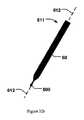
殆どのタッチシステムでは、ユーザはタッチを検知させるために、タッチパネルの表面に指を置く。代替的には、スタイラスが使用されることもある。スタイラスは、典型的には、一端がタッチパネルの表面に押し付けられるように構成されたペン形状の物体である。従来技術によるスタイラスの一例が図3に示されている。スタイラス60を使用することにより、単純な指のタッチよりも改善された選択精度およびポインタ精度を提供することができる。これは、工学的なスタイラス先端160が、人間の指で生じ得るよりも、小さく、かつ/またはタッチパネルとのより規則的な接触面を提供することに起因すると考えられる。また、ペンおよび鉛筆の生涯にわたる使用訓練により、ペン保持位置における手全体の筋肉制御は、ポインタ制御の目的のために、単一の指よりも正確なものとなり得る。 In most touch systems, the user places a finger on the surface of the touch panel to detect a touch. Alternatively, a stylus may be used. The stylus is typically a pen-shaped object configured so that one end is pressed against the surface of the touch panel. An example of a stylus according to the prior art is shown in FIG. Using the
タッチシステムには2種類のスタイラスが存在する。アクティブスタイラスは、通常、信号をホストタッチシステムに送信するためにある形態の電源および電子機器を含むスタイラスである。送信される信号のタイプは変化し得るが、位置情報、圧力情報、傾き情報、スタイラスID、スタイラスタイプ、インク色などを含むことができる。アクティブスタイラス用の電源には、バッテリ、キャパシタ、または誘導結合を介して電力を提供する電場が含まれる。アクティブスタイラスは、電源が無いと、その機能の一部または全部を失うことがある。 There are two types of stylus in the touch system. An active stylus is a stylus that typically includes some form of power and electronics to send signals to the host touch system. The type of signal transmitted can vary, but can include position information, pressure information, tilt information, stylus ID, stylus type, ink color, and the like. The power source for the active stylus includes an electric field that provides power through a battery, capacitor, or inductive coupling. An active stylus may lose some or all of its functionality if there is no power.
ホストシステムは、アクティブスタイラスから電子スタイラスIDを受け取り、そのスタイラスIDと、スタイラスとホストシステムのタッチ面との間の接触位置に関連する位置情報とを関連付けることによって、アクティブスタイラスを容易に識別することができる。 The host system receives an electronic stylus ID from the active stylus and easily identifies the active stylus by associating the stylus ID with location information related to the contact location between the stylus and the touch surface of the host system Can do.
パッシブスタイラスは、電源を有しておらず、ホストシステムと能動的に通信することはない。このため、パッシブスタイラスは、アクティブスタイラスよりも安価に製造でき、メンテナンスを必要としない。しかしながら、印加圧力、傾き情報、スタイラスID、スタイラスタイプ、インク色などの高度な情報をパッシブスタイラスから得ることは、アクティブスタイラスから得るよりも非常に難しい。 The passive stylus does not have a power source and does not actively communicate with the host system. For this reason, the passive stylus can be manufactured at a lower cost than the active stylus and does not require maintenance. However, obtaining advanced information such as applied pressure, tilt information, stylus ID, stylus type, and ink color from a passive stylus is much more difficult than obtaining from an active stylus.
米国特許第6,567,078号は、複数のパッシブスタイラスを、各スタイラスに固有のパターンにより1またはそれ以上のカラーフィルムでマーキングする方法を開示している。カメラは、スタイラス上のカラーマーキングを記録し、使用中のパッシブスタイラスを識別し、スクリーン上に表示されるインク色の適切な選択を決定するように配置されている。 US Pat. No. 6,567,078 discloses a method of marking a plurality of passive styluss with one or more color films according to a pattern unique to each stylus. The camera is arranged to record the color markings on the stylus, identify the passive stylus in use, and determine the appropriate selection of ink colors to be displayed on the screen.
米国特許出願公開第2004/0252091号および米国特許第4,459,476号に記載されているような光学式タッチシステムの場合、スタイラスのような小さい先端を有する物体を識別することが難しいことがある。特に、スタイラス先端は、典型的には小さく(例えば、直径4mmより小さく)、指またはその他の大きな物体と比較して、光信号の減衰量が相対的に小さい。スタイラス先端は、タッチシステムが分解することができる分解能よりも小さい直径を有する場合もある。 In the case of optical touch systems such as those described in U.S. Patent Application Publication No. 2004/0252091 and U.S. Pat. No. 4,459,476, it may be difficult to identify an object with a small tip, such as a stylus. is there. In particular, the stylus tip is typically small (eg, smaller than 4 mm in diameter) and has a relatively small attenuation of the optical signal compared to a finger or other large object. The stylus tip may have a diameter that is smaller than the resolution that the touch system can resolve.
さらに、このようなシステムの信号対雑音比は低いため、固有の再帰性反射材料構成を使用した複数のパッシブスタイラスの各々の識別は困難であり、信頼性も低くなる。 Furthermore, the low signal-to-noise ratio of such a system makes it difficult to identify each of the plurality of passive styluss using a unique retroreflective material configuration and is less reliable.
したがって、上記のような問題点を抱えていない光学式タッチシステムに接触する物体を識別する方法が必要とされている。 Therefore, there is a need for a method for identifying an object that contacts an optical touch system that does not suffer from the above problems.
本発明の目的は、先行技術の上述した欠点の1またはそれ以上を少なくとも部分的に解決することにある。 It is an object of the present invention to at least partially solve one or more of the above-mentioned drawbacks of the prior art.
これらの目的のうちの1またはそれ以上、並びに、以下の記載に現れる別の目的は、独立請求項に係るデータ処理方法、コンピュータ可読媒体、データ処理装置およびタッチ検知装置によって少なくとも部分的に達成されるものであり、その実施形態が従属請求項によって規定される。 One or more of these objects, as well as other objects appearing in the following description, are achieved at least in part by a data processing method, a computer readable medium, a data processing device and a touch sensing device according to the independent claims. And its embodiments are defined by the dependent claims.
本発明の実施形態を、添付の概略図を参照してより詳細に説明する。
本発明は、光学式タッチパネルと、表示装置にタッチ検知性を与える技術の使用に関する。記載全体を通じて、対応する構成要素を識別するために同じ符号を使用する。 The present invention relates to the use of an optical touch panel and a technology that imparts touch sensitivity to a display device. Throughout the description, the same symbols are used to identify corresponding components.
本発明の実施形態を説明する前に、幾つかの定義を与えることとする。
「接触物体」または「接触する物体」は、タッチシステムの1または複数のセンサによって検出されるように、タッチ面に接触する物理的対象またはタッチ面に十分接近した物理的対象である。物理的対象は、有生物または無生物とすることができる。
「相互作用」は、センサにより測定されるパラメータに接触物体が影響を及ぼす場合に生じる。
「タッチ」は、相互作用パターンに見られる相互作用のポイントを示している。
以下の記載を通じて、対応する構成要素を識別するために同じ符号を使用する。
「光照射野」は、エミッタと対応する検出器との間を漂う光である。エミッタは多量の光を多くの方向に発生させることができるが、エミッタから発せられて検出器により測定された光のみが、エミッタおよび検出器のための光照射野を規定する。Before describing embodiments of the present invention, some definitions will be given.
A “contact object” or “contact object” is a physical object that touches or is sufficiently close to the touch surface as detected by one or more sensors of the touch system. The physical object can be living or inanimate.
“Interaction” occurs when a touching object affects the parameters measured by the sensor.
“Touch” indicates the point of interaction found in the interaction pattern.
Throughout the following description, the same symbols are used to identify corresponding components.
A “light field” is light drifting between an emitter and a corresponding detector. The emitter can generate a large amount of light in many directions, but only the light emitted from the emitter and measured by the detector defines the light field for the emitter and detector.
図1は、図3のFTIRベースのタッチ装置または図2のIR光学式タッチ装置に対応し得る光学式タッチ装置の平面図である。エミッタ30aは、タッチ面20の周縁の周りに配置され、タッチパネル10のタッチ面20にわたって光を投影する。検出器30bは、タッチ面20の周縁の周りに配置され、伝播する光の一部を受信する。各エミッタ30aからの光は、複数の光路50上の多数の異なる検出器30bに伝播する。 FIG. 1 is a plan view of an optical touch device that may correspond to the FTIR-based touch device of FIG. 3 or the IR optical touch device of FIG. The
図3は、従来技術による、ここでは「ガラス内」システムと呼ばれるFTIRベースのタッチ装置の断面を示している。図2は、従来技術による、ここでは「表面上」システムと呼ばれるIR光学式タッチ装置の断面を示している。図3および図2に示す例示的な装置の各々において、物体60は、少なくとも1の光路50に沿って伝播する光を減衰させるものとなる。図2の例では、物体60は、少なくとも1の光路50上の光を完全に遮ることさえある。 FIG. 3 shows a cross-section of a prior art FTIR-based touch device, referred to herein as an “in-glass” system. FIG. 2 shows a cross section of an IR optical touch device, referred to herein as an “on-surface” system, according to the prior art. In each of the exemplary devices shown in FIGS. 3 and 2, the
光路50は、概念的には、図1に示すように、エミッタ30aと検出器30bのペア間に、タッチ面20を横切ってタッチ面20の周縁に延びる「検出ライン」として表すことができる。このため、検出ライン50は、タッチ面20への光路50の投影に対応する。エミッタ30aおよび検出器30bは、平面図に見られるように、タッチ面20上に検出ライン50のグリッド(「検出グリッド」)を共同で規定する。検出グリッド内の交点の間隔は、タッチ検知装置100の空間分解能、すなわちタッチ面20上で検出可能な最小の物体を規定する。検出ラインの幅は、エミッタおよび対応する検出器の幅の関数である。幅の広いエミッタからの光を検出する幅の広い検出器は、より広い表面カバレッジを有する幅の広い検出ラインを提供し、接触カバレッジを提供しない検出ラインの間の空間を最小にする。幅の広い検出ラインの欠点は、接触精度が低下し、信号対雑音比が低下することである。 Conceptually, the
本明細書で使用されるエミッタ30aは、例えば、ダイオードレーザ、VCSEL(垂直キャビティ面発光レーザ)、LED(発光ダイオード)、白熱ランプおよびハロゲンランプなど、所望の波長範囲の放射を発することができる任意の種類のデバイスとすることができる。エミッタ30aは、光ファイバの端部によって形成されるものであってもよい。エミッタ30aは、任意の波長範囲の光を生成することができる。以下の実施例では、光が赤外線(IR)、すなわち約750nm以上の波長であると仮定する。同様に、検出器30bは、光検出器、CCDデバイス、CMOSデバイスなど、(同じ波長範囲内の)光を電気信号に変換することができる任意のデバイスとすることができる。 As used herein, the
検出器30bは、共同で出力信号を提供し、出力信号は、信号プロセッサ130により受信されて、サンプリングされる。出力信号は、「透過値」とも呼ばれる数多くのサブ信号を含み、その各々が、光エミッタ30aの1つから発せられて光検出器30bの1つによって受信される光のエネルギーを示している。実施形態に応じて、信号プロセッサ130は、個々の透過値を分離するために出力信号を処理しなければならない場合もある。透過値は、個々の検出ライン50上の検出器30bにより受信された光の受信エネルギー、強度またはパワーを示している。物体が検出ライン50に接触するときはいつでも、この検出ライン上の受信エネルギーは低減または「減衰」される。物体が表面上システムの検出ラインの幅全体を遮る場合、検出ラインは完全に減衰または閉塞されるものとなる。
好ましい実施形態では、タッチ装置が図2に従って配置される。エミッタ30aによって発せられた光は、透過パネル10内で光を全反射させることがないように、透過パネル10を通って伝送される。光は、タッチ面20を通って透過パネル10から出射し、エッジ反射器70の反射面80により反射されて、タッチ面20と平行な平面内の経路50に沿って移動する。その後、光は、透過パネル10の反対側のエッジでエッジ反射器70の反射面80により屈折するまで進み続け、そこで、光は、透過パネル10を通って下方に戻るように屈折して検出器30b上に至る。面20に接触する物体60(任意には物体先端部160を有する物体)は、面上の物体の位置と交差する光路50を塞ぎ、その結果、検出器30bにおいて減衰された光信号が受信されるものとなる。 In a preferred embodiment, the touch device is arranged according to FIG. The light emitted by the
図4は、エミッタ30aから検出器30bに進む光が反射面80間に光照射野90を形成する方法を示している。好ましい実施形態では、反射面80の上端がタッチ面20の2mm上にある。これは、2mmの深さの光照射野90をもたらす。2mmの深さの照射野は、物体が、タッチ面に到達して光を最も減衰させるべく光照射野内に移動するのに必要な距離を最小にするため、この実施形態には有利である。距離が小さいほど、物体が光照射野に入ってから面に接触するまでの時間が短くなる。これは、光照射野にゆっくりと入る大きな物体と光照射野に素早く入る小さな物体とを区別するのに、特に有利である。光照射野に入る大きな物体は、最初に、より小さな物体が光照射野内に完全に入り込むのと同様の減衰を引き起こす。物体が移動する距離が短いほど、各物体の代表的な減衰信号が観測されるまでに必要なフレームが少なくなる。この効果は、光照射野が0.5mm−2mmの深さのときに特に顕著である。 FIG. 4 shows a method in which light traveling from the
図3に示される構成は代替的な実施形態であるが、以下に述べるスタイラスの区別の概念も同様に適用される。この装置は、透過パネル10内からタッチ面20を照らすように、透過パネル10内の光を光エミッタ30aから光センサまたは検出器30bに送信することによって動作する。透過パネル10は、1またはそれ以上の層の固体材料からなり、任意の形状を有することができる。透過パネル10は、光が内部反射によって経路50に沿って伝播する内部放射伝播チャネルを規定する。透過パネル10の表面に接触する物体は、タッチの位置で内部反射効果のフラストレーションを引き起こし、全反射によりパネルを通って進む光の一部が、物体によって散乱または吸収される。このようにして、パネルを通って進む光のビームは、タッチの位置で減衰される。 Although the configuration shown in FIG. 3 is an alternative embodiment, the concept of stylus discrimination described below applies as well. This device operates by transmitting light in the
別段の記載がない限り、本明細書に記載の実施形態は、図2に示す構成に適用される。しかしながら、それらの実施形態の幾つかは、図3に示す構成にも適用され得る。 Unless stated otherwise, the embodiments described herein apply to the configuration shown in FIG. However, some of those embodiments can also be applied to the configuration shown in FIG.
信号プロセッサ130は、位置(例えば、x、y座標系における位置)、形状または面積など、接触する物体の特性を判定すべく透過値を処理するように構成することができる。この判定は、米国特許第7,432,893号および国際公開第2010/015408号に開示されているような、減衰された検出ラインに基づく直接的な三角測量や、各減衰値が光減衰の局所的度合いを示すものとして、タッチ面20全体にわたって減衰値の分布(簡略化のため、「減衰パターン」と称する)を再現するためのより進んだ処理を含むことができる。減衰パターンは、物体の位置、形状または面積の判定のために、信号プロセッサ130または別個の装置(図示省略)によってさらに処理されるものであってもよい。減衰パターンは、透過値に基づく画像再構成のための任意の利用可能なアルゴリズムによって生成することができ、そのようなアルゴリズムには、トモグラフィ再構成法、例えば、フィルタ補正逆投影法、FFTベースのアルゴリズム、ART(代数的再構成法)、SART(連立代数的再構成法)などが含まれる。代替的には、減衰パターンは、1つまたはそれ以上の基底関数を適合させることによって、かつ/またはベイズ・インバージョンなどの統計的方法によって生成することができる。タッチ判定用に設計されたそのような再構成関数の例は、国際公開第2009/077962号、国際公開第2011/049511号、国際公開第2011/139213号、国際公開第2012/050510号および国際公開第2013/062471号に見出される。これら文献のすべてが引用により本明細書に援用されるものとする。 The
簡潔にするために、「信号プロセッサ」という用語は、検出器から信号を受信してから、タッチ座標、タッチ特性などを含むタッチの判定を出力するまでに必要とされる様々な処理段階を実行するための1またはそれ以上の処理構成要素を述べるために、全体を通して使用される。本開示の処理段階は、単一の処理ユニット(対応するメモリユニットを有する処理ユニット)上で実行することができるが、本開示は、複数の処理ユニットや、遠隔に配置された処理ユニットも対象にすることを意図している。 For brevity, the term “signal processor” performs the various processing steps required from receiving a signal from a detector to outputting a touch decision including touch coordinates, touch characteristics, etc. Used throughout to describe one or more processing components to do. Although the processing steps of the present disclosure can be performed on a single processing unit (processing unit having a corresponding memory unit), the present disclosure is also directed to multiple processing units and remotely located processing units. Is intended to be.
図示の例では、装置100は、エミッタ30aの作動と、場合によっては検出器30bからのデータの読み出しを選択的に制御するように接続されたコントローラ120も含む。実施形態に応じて、エミッタ30aおよび/または検出器30bは、例えば米国特許第8,581,884号に開示されているように、順番にまたは同時に作動させることができる。信号プロセッサ130およびコントローラ120は、別々のユニットとして構成されるようにしても、あるいは単一のユニットに組み込まれるようにしてもよい。信号プロセッサ130およびコントローラ120の一方または両方は、処理ユニット140によって実行されるソフトウェアによって少なくとも部分的に実施されるものであってもよい。 In the illustrated example, the
図5は、好ましい実施形態に係るフローチャートを示している。 FIG. 5 shows a flowchart according to a preferred embodiment.
図5のステップ510では、信号プロセッサ130が、検出器30bからの出力信号を受信して、サンプリングする。 In
ステップ520では、出力信号が、透過値(または「透過信号」)を求めるために処理される。上述したように、透過値は、個々の検出ライン50上の検出器30bによって受信された光の受信エネルギー、強度またはパワーを表している。 In
ステップ530では、信号プロセッサ130が、透過値を処理して、タッチ面上の1またはそれ以上の接触する物体の存在を判定するように構成される。好ましい実施形態では、信号プロセッサ130が、透過値を処理して、タッチ面における減衰フィールドの2次元推定、すなわち減衰値の空間分布を生成するように構成される。減衰フィールドでは、接触する各物体が、通常、変化した減衰の領域のように見える。減衰フィールドから、2次元のタッチデータを抽出し、1またはそれ以上のタッチ位置を識別することができる。透過値は、トモグラフィ再構成アルゴリズムに従って処理され、それにより、減衰フィールドの2次元推定を生成することができる。 In
一実施形態では、信号プロセッサ130が、タッチ面全体に対して減衰フィールドを生成するように構成されるものであってもよい。代替的な実施形態では、信号プロセッサ130が、タッチ面のサブセクションについて減衰フィールドを生成するように構成され、サブセクションが、透過値の処理中に決定される1またはそれ以上の基準に従って選択されるものであってもよい。 In one embodiment, the
ステップ540では、信号プロセッサ130が、物体がタッチ面に触れることに起因する光のビームの減衰に対応する減衰値を含む、各タッチ位置における物体の特性を判定する。 In
一実施形態では、減衰値は以下のようにして求められる。先ず、減衰パターンが、例えば任意の公知技術を用いて、ピークの検出のために処理される。一実施形態では、ノイズを抑制するために、グローバルまたはローカル閾値が減衰パターンに最初に適用される。閾値を上回る減衰値を有する領域は、極大値を見付けるためにさらに処理される。識別された最大値は、例えば2次元2次多項式またはガウスベル形状を減衰値に当てはめることによって、または減衰値の慣性楕円を見付けることによって、タッチ形状および中心位置の判定のためにさらに処理されるものであってもよい。クラスタリングアルゴリズム、エッジ検出アルゴリズム、標準ブロブ検出、ウォータシェディング技術、フラッドフィル技術など、当技術分野で周知のその他の技術も数多く存在する。ステップ540では、検出した各ピークについての位置、減衰、サイズ、形状の値を含む、ピークデータの収集がもたらされる。減衰値は、ピーク形状内の最大減衰値または減衰値の加重和から計算することができる。 In one embodiment, the attenuation value is determined as follows. First, the attenuation pattern is processed for peak detection using, for example, any known technique. In one embodiment, a global or local threshold is first applied to the attenuation pattern to suppress noise. Regions with attenuation values above the threshold are further processed to find local maxima. The identified maximum value is further processed for touch shape and center position determination, for example by fitting a two-dimensional quadratic polynomial or Gaussian bell shape to the attenuation value, or finding an inertia ellipse of the attenuation value It may be. There are many other techniques known in the art, such as clustering algorithms, edge detection algorithms, standard blob detection, water shedding techniques, flood fill techniques. Step 540 results in a collection of peak data, including position, attenuation, size, and shape values for each detected peak. The attenuation value can be calculated from the maximum attenuation value within the peak shape or a weighted sum of the attenuation values.
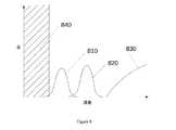
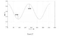
物体について記録された減衰値は、ノイズ、物体の角度、物体の材料或いはその他の多くの理由により変化し得る。図6は、タッチ面に与えられた8つの固有の物体の各々についての減衰値のカウントを示すヒストグラムである。各物体は、記録された減衰値の周波数のほぼベル形状の分布を示している。特に各物体についての多数の減衰値が記録されている場合には、記録された減衰値から異なる物体を区別することが可能であることが、図6から明らかである。 The attenuation values recorded for an object may vary due to noise, object angle, object material, or many other reasons. FIG. 6 is a histogram showing the count of attenuation values for each of the eight unique objects applied to the touch surface. Each object exhibits a substantially bell-shaped distribution of the recorded attenuation frequency. It is clear from FIG. 6 that different objects can be distinguished from the recorded attenuation values, especially when a large number of attenuation values for each object are recorded.
特定の物体は、その他の物体よりも減衰値の分布が広くなる場合がある。図7は、タッチ面に当てられた2つの物体、スタイラスおよび指からの光ビームの減衰の測定値を示すヒストグラムである。ベル形状の分布値710は、タッチ面に当たる特別に設計されたスタイラス先端の減衰値を示している。分布720は、タッチ面に当たる様々な指の集まりの減衰値を示している。人は異なるサイズの指を有し、幾つかの指が他の指よりも脂性である場合もあるため、分布720の物体からの可能性のある減衰値の範囲は、特別に設計されたスタイラス先端についての可能性のある減衰値よりも遥かに広い。ゾーン730は、システムが信頼性をもって記録するには小さ過ぎる減衰値を示している。典型的な例では、ゾーン730は、1.8*10−3より小さい減衰値をカバーする(注:本明細書に記載されている全ての減衰値はmm−1の単位を有するが、多くの異なる方法で減衰を測定できることが理解されよう)。これは、システムの接触分解能に応じて、0.5mmより小さい物体に変換することができる。このため、本発明の好ましい実施形態は、ゾーン730の値より大きいが、分布720が占める減衰値の範囲よりも小さい範囲の減衰値を提供するように構成されたスタイラス先端を備える。例えば、1.8*10−3<スタイラス先端の減衰<2.0*10−2A specific object may have a wider distribution of attenuation values than other objects. FIG. 7 is a histogram showing measured attenuation of light beams from two objects, a stylus and a finger applied to the touch surface. The bell-shaped
図8は、タッチ面に当てられた3つの物体、第1のスタイラス、第2のスタイラスおよび指からの光ビームの減衰の測定値を示すヒストグラムである。このため、本開示の実施例においてタッチ面に接触する物体60は、スタイラス、または複数のスタイラス、若しくは指または複数の指などの人間の手の一部である。図7と同様に、ベル形状の値の分布810は、タッチ面に当たる第1の特別に設計されたスタイラス先端の減衰値を示している。分布830は、タッチ面に当たる指の減衰値を示している。ゾーン840は、システムが信頼性をもって記録するには小さ過ぎる減衰値を示している。ベル形状の値の分布820は、タッチ面に当たる第2の特別に設計されたスタイラス先端の減衰値を示している。したがって、本発明の別の実施形態は、ゾーン840の値よりも大きいが、第2のスタイラス先端によって占められる減衰値820の範囲よりも小さい範囲の減衰値を提供するように構成された第1のスタイラス先端を備える。第2のスタイラス先端は、分布810によって占められる値よりも大きいが、分布830によって占められる減衰値の範囲よりも小さい範囲の減衰値を提供するように構成されている。例えば、1.8*10−3<第1のスタイラス先端の減衰<7.2*10−3<第2のスタイラス先端の減衰<2.0*10−2FIG. 8 is a histogram showing measured attenuation of light beams from three objects, a first stylus, a second stylus and a finger applied to the touch surface. Thus, in an embodiment of the present disclosure, the
好ましい実施形態では、信号プロセッサ130は、複数の物体IDをメモリに格納するように構成されており、各物体IDが、関連する減衰値の範囲を有している。以下の例では、関連付けられた物体IDを持つ3種類の物体が示されている。 In a preferred embodiment, the

好ましい実施形態では、各物体IDが、減衰最大値および減衰最小値によって定義される減衰値の範囲を有する。物体IDは、任意選択的に、関連する物体の特性を定義する更なる値を含むことができ、それには、認識された物体のタイプ、出力のタイプ(例えば、ブラシタイプ、インク色、選択タイプなど)が含まれる。 In a preferred embodiment, each object ID has a range of attenuation values defined by a maximum attenuation value and a minimum attenuation value. The object ID can optionally include additional values that define the properties of the associated object, including the recognized object type, output type (eg, brush type, ink color, selection type). Etc.).
ステップ550では、信号プロセッサ130が、各タッチ位置を物体IDに対応付ける。これは、各タッチ位置の減衰値を、対応付ける物体IDの範囲と対応付けることによって行われる。すなわち、1.2*10−2の減衰値を有するタッチ位置は、物体ID001に対応付けられるものとなる。一実施形態では、特定の値を超えるすべての値の範囲を有する物体IDが存在する。これにより、物体IDの通常の範囲を超える減衰値を持つすべての物体を、同じ「デフォルト大型物体」の物体IDを使用して特定することが可能になる。同様に、一実施形態では、特定の値未満のすべての値の範囲を持つ物体IDが存在し、これにより、非常に低い減衰値の物体を一般的な「デフォルト小型物体」の物体IDで特定することが可能になる。In
ステップ560では、信号プロセッサ130が、タッチ位置および各位置の対応する物体IDを含むタッチデータを出力する。 In
タッチの減衰値を物体IDに対応付ける場合、物体が面に接触したときに物体によって引き起こされる光の減衰を正確に反映する安定した減衰値を使用することが重要である。図2に示す実施形態のような「表面上」システムでは、光照射野90が深さを有し、よって物体が、タッチ面に接触する前に光照射野を通って所定の距離移動しなければならない。その結果、物体が光照射野に入る時と物体がタッチ面に接触する時との間の所定の期間が、物体に起因する減衰が増加しそうな場合に存在する。この期間中に測定される減衰値は、物体がタッチ面に接触しているときに物体の光減衰を正確に反映しない可能性がある。本発明の一実施形態では、ステップ540が、物体の減衰値が安定していると判定されるまで遅延される。一実施形態では、物体の減衰値が、少なくとも3つのフレームの間、各フレームにおいて10%を超えて変化していないときに、安定していると判定される。 When associating a touch attenuation value with an object ID, it is important to use a stable attenuation value that accurately reflects the attenuation of light caused by the object when the object touches the surface. In an “on the surface” system, such as the embodiment shown in FIG. 2, the
物体が光照射野内に降下されるに連れて、より多くの光を徐々に遮るようになる。その結果、物体に起因する光の減衰は、物体が接触面に当たるまで増加する。従って、減衰の勾配(すなわち、減衰の変化率)は、物体がタッチ面に向かって移動するときは、物体が面に接触して平らになるまで、プラスである。図9は、hmax−hの距離だけ光照射野90内に移動した先端部160を有する物体60を示している。図10は、「タッチダウン」イベント1040(すなわち、タッチ面に接触物体を付ける)および「タッチアップ」イベント1050(すなわち、接触物体を引き上げてタッチ面から引き離す)間の物体の減衰値1020を示している。タッチ面からの物体の対応する高さh(ライン1010として示す)も示されている。減衰勾配(すなわち、時間に対する減衰値の変化率)を示すライン1030は、タッチダウンイベントとタッチアップイベントの両方に対する典型的な減衰勾配シグネチャを示している。減衰勾配シグネチャは、タッチダウンまたはタッチアップイベント中の減衰勾配値の形状である。As the object is lowered into the light field, it gradually blocks more light. As a result, light attenuation due to the object increases until the object hits the contact surface. Thus, the slope of attenuation (ie, the rate of change of attenuation) is positive as the object moves toward the touch surface until the object contacts the surface and becomes flat. FIG. 9 shows an
したがって、本発明の好ましい実施形態では、信号プロセッサ130が、物体の減衰値が安定していること、および/またはイベントの減衰勾配シグネチャ(図10における時間1040に示される)に応じてタッチダウンイベントが発生したことを判定するように構成されている。好ましい実施形態では、タッチダウンイベントに対応する減衰勾配シグネチャが、第1の減衰勾配の第1の期間、より高い減衰勾配の第2の期間、および第2の期間よりも低い減衰勾配の第3の期間である。 Accordingly, in a preferred embodiment of the present invention, the
一実施形態では、物体の減衰値が第1の減衰値閾値を超えたときに、タッチダウンイベントが発生したと判定される。しかしながら、上記の方法を用いることにより、この閾値が満たされる前に、タッチダウンイベントが発生したという判定が可能である。物体の減衰値が第1の減衰値閾値を下回るが、減衰勾配シグネチャが、単一フレームにおいて第1の減衰値閾値の20%またはそれ以上のより高い減衰勾配を有すると観察される場合、物体の減衰値が安定していると判定され、かつ/またはタッチダウンイベントが発生したと判定される。 In one embodiment, it is determined that a touchdown event has occurred when the attenuation value of the object exceeds a first attenuation value threshold. However, by using the above method, it is possible to determine that a touchdown event has occurred before this threshold is satisfied. If the attenuation value of the object is below the first attenuation value threshold, but the attenuation gradient signature is observed to have a higher attenuation gradient of 20% or more of the first attenuation value threshold in a single frame, the object Is determined to be stable and / or it is determined that a touchdown event has occurred.
「タッチアップ」イベントの間、物体が光照射野から引き上げられるに連れて、物体の減衰値が減少する。上記と同様に、このイベントの減衰勾配シグネチャ(図10における時間1050に示される)は、認識され、それに応じて実行される。したがって、本発明の好ましい実施形態では、信号プロセッサ130が、物体の減衰値がゼロに減少したこと、および/またはイベントの減衰勾配シグネチャに応じてタッチアップイベントが発生したことを判定するように構成される。好ましい実施形態では、タッチアップイベントに対応する減衰勾配シグネチャが、第1の減衰勾配の第1の期間、負の減衰勾配の第2の期間、および第1の減衰勾配に対応する減衰の第3の期間である。 During the “touch-up” event, the attenuation value of the object decreases as the object is lifted from the light field. As above, the decay slope signature of this event (shown at
一実施形態では、物体の減衰値が第2の減衰値閾値未満に低下したと判定されたときに、タッチアップイベントが発生したと判定される。しかしながら、上記の方法を用いることにより、この閾値が満たされる前に、タッチアップイベントが発生したという判定が可能である。物体の減衰値が第2の減衰値閾値を上回るが、減衰勾配シグネチャが、単一フレームにおいて第2の減衰値閾値の20%またはそれ以上のより負の減衰勾配を有すると観察される場合、タッチアップイベントが発生したと判定される。 In one embodiment, it is determined that a touch-up event has occurred when it is determined that the attenuation value of the object has dropped below a second attenuation value threshold. However, by using the above method, it is possible to determine that a touch-up event has occurred before this threshold is satisfied. If the attenuation value of the object is above the second attenuation value threshold, but the attenuation gradient signature is observed to have a more negative attenuation gradient of 20% or more of the second attenuation value threshold in a single frame, It is determined that a touch-up event has occurred.
好ましい実施形態では、物体のタッチアップ/ダウンイベントをトリガするのに必要な減衰勾配値は、物体に近接するその他の閉塞物体の存在に応じて増減することができる。好ましい実施例では、シグネチャの第2の期間の減衰勾配が、タッチ面上のその他の閉塞物体に近接している物体についてタッチダウンイベントをトリガするためにより大きな値を必要とするように増大される。一実施形態では、より高い減衰勾配が、10cmまでの半径内の追加的なタッチ回数に応じて、直線的に増減される。その半径は、スクリーンサイズ、タッチ分解能、および環境ノイズに応じて選択することができる。 In a preferred embodiment, the attenuation slope value required to trigger an object touch up / down event can be increased or decreased depending on the presence of other occluded objects in proximity to the object. In the preferred embodiment, the decay slope of the second period of the signature is increased to require a larger value to trigger a touchdown event for objects in proximity to other occluded objects on the touch surface. . In one embodiment, the higher attenuation gradient is linearly increased or decreased in response to additional touches within a radius of up to 10 cm. The radius can be selected depending on screen size, touch resolution, and environmental noise.
「フック(Hooks)」は、ユーザのタッチ入力が急激に変化するとき、例えば描画しているとき又は文字を書いているときに、経時的なユーザタッチ入力の座標のフローにおいて観察される問題である。「フック」の例は、ユーザが線を引くのを終了し、接触物体をパネルの表面から持ち上げ、接触物体の動く方向を急速に変更して次の線を引き始める場合である。「フック」は、ユーザーの接触物体の新しい方向を指し示すストロークの終わりに見られる小さなアーチファクトである。フックを最小化する方法が提案される。本発明の好ましい実施形態では、負の減衰勾配が観察されたときに、タッチ座標が物体の位置で更新されずに、物体の位置の座標が記憶される。物体の減衰値が閾値未満に低下する場合、記憶された座標が破棄され、「タッチアップ」イベントが通知される。物体の減衰値が閾値未満に低下せず、その後に正の減衰勾配が観測される場合、その間に記憶されたタッチ座標が出力され、タッチ座標が以前と同じように出力され続ける。好ましい実施形態では、この方法は、タッチ面の平面内においてタッチ面に接触する物体の移動方向が変化している場合にのみ使用される。この実施形態では、物体の最後のタッチ座標から現在の座標までのベクトルαが求められる。最後の座標の前のタッチ座標から最後の座標までの第2のベクトルβが求められる。ベクトルαおよびβは、相互作用が移動している方向とそれがどのように変化しているかの判定を可能にする。物体の方向の急な変化は、αとβの内積<0をもたらし得る。一実施形態では、この条件が満たされる場合、タッチ面に接触する物体の移動方向が大きく変化したことが判定され、その後、フックを最小にする上記方法が適用される。 “Hooks” is a problem observed in the flow of user touch input coordinates over time when the user's touch input changes abruptly, for example when drawing or writing characters. is there. An example of a “hook” is when the user finishes drawing a line, lifts the contact object off the surface of the panel, rapidly changes the direction of movement of the contact object and begins to draw the next line. A “hook” is a small artifact seen at the end of a stroke that points to the new direction of the user's contact object. A method for minimizing hooks is proposed. In a preferred embodiment of the present invention, when a negative decay gradient is observed, the coordinates of the object position are stored without the touch coordinates being updated with the object position. If the attenuation value of the object falls below the threshold, the stored coordinates are discarded and a “touch up” event is notified. If the attenuation value of the object does not drop below the threshold and a positive attenuation gradient is subsequently observed, the touch coordinates stored during that time are output and the touch coordinates continue to be output as before. In a preferred embodiment, this method is used only when the direction of movement of the object that contacts the touch surface is changing in the plane of the touch surface. In this embodiment, a vector α from the last touch coordinate of the object to the current coordinate is obtained. A second vector β from the touch coordinates before the last coordinate to the last coordinate is obtained. The vectors α and β allow a determination of the direction in which the interaction is moving and how it is changing. A sudden change in the direction of the object can result in an inner product <0 of α and β. In one embodiment, if this condition is met, it is determined that the direction of movement of the object touching the touch surface has changed significantly, and then the above method of minimizing the hook is applied.
物体の減衰値は、物体が面に接触することによって減衰される光に関する情報を提供するが、本発明の幾つかの実施形態は、物体の性質および/または位置の真の反映を提供するために、減衰値を補正することを必要とする。 While object attenuation values provide information about the light that is attenuated when an object touches a surface, some embodiments of the present invention provide a true reflection of the nature and / or position of the object In addition, it is necessary to correct the attenuation value.
本発明の一実施形態では、減衰値が、物体がタッチ面に触れることによって生じる光の減衰および補正値に応じて判定される。減衰値は、上述したステップ540のように判定されるが、減衰値は、補正値と、ピーク形状内の最大減衰値または減衰値の加重合計から計算される。 In one embodiment of the invention, the attenuation value is determined in response to light attenuation and correction values caused by an object touching the touch surface. The attenuation value is determined as in
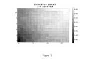
図1に示すシステムの特定の構成では、タッチ面の特定の位置が、その他のものよりも低い減衰値をもたらす可能性がある。特に、スクリーンの縁に向かう減衰値は中心部よりも低い可能性が高い。様々な要因がこれを引き起こす場合がある。1つは、特定のトモグラフィ再構成アルゴリズムの効率的な実施が近似を行うことで、パネルの縁に向かって再構成された減衰値が結果として低くなるというものである。一例では、パネルのコーナーにおける減衰値が、パネルの中央部に位置する減衰値の30%程度の低さとなり得る。図11は、タッチ面のコーナーからの物体の距離に対する、長方形のタッチ面に接触する物体の減衰値(相対減衰として示される)のグラフを示している。このため、本発明の好ましい実施形態は、補正値が、少なくともタッチ面上の物体の位置の関数であることを提供する。一実施形態では、補正値は、タッチ面の中心点からタッチ位置までの距離の関数として決定される。代替的には、補正値は、タッチ面の最も近いコーナーからタッチ位置までの距離の関数として決定されるものであってもよい。 In the particular configuration of the system shown in FIG. 1, certain locations on the touch surface may result in lower attenuation values than others. In particular, the attenuation value towards the edge of the screen is likely to be lower than in the center. Various factors can cause this. One is that an efficient implementation of a particular tomographic reconstruction algorithm approximates, resulting in a lower attenuation value reconstructed towards the edge of the panel. In one example, the attenuation value at the corner of the panel can be as low as 30% of the attenuation value located at the center of the panel. FIG. 11 shows a graph of the attenuation value (shown as relative attenuation) of an object touching a rectangular touch surface against the distance of the object from the corner of the touch surface. For this reason, a preferred embodiment of the present invention provides that the correction value is at least a function of the position of the object on the touch surface. In one embodiment, the correction value is determined as a function of the distance from the center point of the touch surface to the touch position. Alternatively, the correction value may be determined as a function of the distance from the closest corner of the touch surface to the touch position.
タッチの位置と必要な補正値との間の関係は、エミッタおよび検出器の配置の複合関数であってもよい。図12は、接触する物体の相対減衰を示す矩形タッチ面のコーナーのヒートマップを示している。座標(0,0)で触れると、物体は相対的に小さな減衰を発生させる。座標(10,15)で触れると、遥かに大きな減衰量が発生する。 The relationship between the position of the touch and the required correction value may be a composite function of emitter and detector placement. FIG. 12 shows a heat map of the corner of the rectangular touch surface showing the relative attenuation of the contacting object. When touched at coordinates (0,0), the object produces a relatively small attenuation. When touching at coordinates (10, 15), a much larger attenuation occurs.
その結果、本発明の好ましい実施形態は、タッチ面上の対応するタッチの位置の関数として補正値を計算することを提供する。代替的な実施形態では、補正マップを使用して、タッチ面上の位置に基づき補正値が決定される。補正マップは、タッチ面の大きさに対応する二次元画像を含むことができ、ピクセル値が補正値に対応する。その後、タッチ位置が補正マップ上の対応するピクセルを判定するために使用され、その位置のピクセル値が対応する補正値を提供する。好ましい実施形態では、補正マップが、タッチ判定システムのタッチ分解能以下の分解能を有する。補正マップは、好ましくは事前に生成されるが、環境および性能変数の関数として動的に生成されるものであってもよい。 As a result, preferred embodiments of the present invention provide for calculating correction values as a function of the position of the corresponding touch on the touch surface. In an alternative embodiment, a correction map is used to determine a correction value based on a position on the touch surface. The correction map can include a two-dimensional image corresponding to the size of the touch surface, and the pixel value corresponds to the correction value. The touch location is then used to determine the corresponding pixel on the correction map, and the pixel value at that location provides the corresponding correction value. In a preferred embodiment, the correction map has a resolution that is less than or equal to the touch resolution of the touch determination system. The correction map is preferably generated in advance, but may be generated dynamically as a function of environment and performance variables.
信号プロセッサ130は、補正マップ内の予め規定された補正値間の補正マップのxおよびy方向の補間によって補正マップ上のある位置における補正値を決定するように構成することができる。このため、補正値の粗いグリッドを有することが可能であり、その後に、粗いグリッドに対する補間を使用して、特定の座標における補正値を得ることが可能である。 The
補正値は、位置のグリッド内の各位置について決定されるものであってもよく、その場合、グリッドのピッチ、すなわちグリッド内のセルの寸法によって補正マップの分解能が決定される。ピッチは、補正マップ内の位置の関数として変化するものであってもよい。例えば、粗いグリッド、すなわちより高いピッチでの双線形補間は、マップの中心部で機能するかもしれないが、縁部および特にコーナーの近傍では、減衰変動を正確に捕捉するために、有利にはピッチを減少させるようにしてもよい。 The correction value may be determined for each position in the position grid, in which case the resolution of the correction map is determined by the pitch of the grid, that is, the dimensions of the cells in the grid. The pitch may vary as a function of position in the correction map. For example, a coarse grid, i.e. bilinear interpolation at a higher pitch, may work in the center of the map, but advantageously in the edges and especially near the corners, to accurately capture attenuation variations The pitch may be reduced.
接触物体の記録された減衰に影響を及ぼす別の変数は、接触する物体がタッチ面を横切って移動する速度である。各光路の光減衰は、一連のフレームにわたって順次記録される。このため、特定の位置を横切るすべての光路の減衰が測定される前に、十分に速い移動物体が特定の位置から離れることがある。その結果、移動物体は、より弱い減衰信号を生成する可能性がある。図13は、タッチ面を横切る物体の速度に対する物体の記録された減衰値のグラフを示している。速い移動物体ほど弱い減衰値を生成する可能性が高いという関係を見ることができる。したがって、本発明の好ましい実施形態は、少なくともタッチ面を横切る物体の速度の関数として決定される補正値に応じて減衰値を計算することを提供する。 Another variable that affects the recorded attenuation of the touching object is the speed at which the touching object moves across the touch surface. The optical attenuation of each optical path is recorded sequentially over a series of frames. Thus, a sufficiently fast moving object may leave the specific position before the attenuation of all optical paths across the specific position is measured. As a result, the moving object may generate a weaker attenuation signal. FIG. 13 shows a graph of the recorded attenuation value of an object against the velocity of the object across the touch surface. It can be seen that the faster moving objects are more likely to generate weaker attenuation values. Accordingly, preferred embodiments of the present invention provide for calculating an attenuation value in response to a correction value determined at least as a function of the velocity of an object across the touch surface.
物体の速度と記録された減衰値との間の関係は、タッチ面上の移動物体の位置によって複雑になる可能性があるため、本発明の実施形態は、タッチ面上の物体の位置および速度の両方の関数として補正値を決定することを提供する。 Since the relationship between the velocity of the object and the recorded attenuation value can be complicated by the position of the moving object on the touch surface, embodiments of the present invention provide the position and velocity of the object on the touch surface. It is provided to determine the correction value as a function of both.
補正値は、光照射野の深さ(hmax)の関数であってもよい。これにより、同時に使用される異なる物体の分類が改善される。例えば、円錐形のスタイラス先端が使用される場合、減衰は、長手方向において均一な厚さを有する先端よりも大きな程度まで、現在の光照射野の高さの影響を受ける。このため、光照射野の高さの差を補正することによって、光照射野の高さの影響が最小限に抑えられるため、異なる先端を有するスタイラスを区別することがより容易になる。The correction value may be a function of the light field depth (hmax ). This improves the classification of different objects used simultaneously. For example, if a conical stylus tip is used, the attenuation is affected by the current light field height to a greater extent than a tip having a uniform thickness in the longitudinal direction. For this reason, by correcting the difference in height of the light field, the influence of the height of the light field is minimized, so that it becomes easier to distinguish styluses having different tips.
信号プロセッサ130は、光検出器30bの出力信号に基づいて光照射野の深さ(hmax)を求めるように構成することができる。より反りのあるタッチ面20とすること、すなわちタッチ面のユーザに向かう方向により凹状とすることにより、光検出器30bによって検出される信号強度が増加する。また、反りの増加は、光照射野の高さの増加にも関連している。このため、タッチ面の反りに応じて出力信号の増減を検出するように信号プロセッサ130を構成することにより、光照射野の高さを推定することができる。その後、光照射野の高さの推定値は、上述した光照射野の高さ補正への入力として使用することができる。The
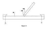
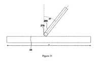
物体がタッチ面に接触することにより光減衰に影響を及ぼし得る別の要因は、物体先端の形状と、先端がタッチ面20に当たるときの角度である。図14は、丸い断面を有する先端が平らのスタイラス260を示している。図15および図16は、端部およびその斜めから見た、平坦な先端270を有するスタイラス260をそれぞれ示している。図17は、タッチ面の法線に対して傾くことなくタッチ面20に当たる平坦な先端のスタイラス260を上から見た斜視図を示している。図18および図19は、面20のy軸およびx軸に沿って見た、先端が平坦なスタイラス先端270をそれぞれ示している。平坦な先端のスタイラス先端270の輪郭は、y軸に沿って見たときと、x軸に沿って見たときで同じであることは明らかである。このため、物体と交差するx軸とほぼ平行な経路(例えば、図17のタッチ面20の左端から始まり、タッチ面の右端で終わる光路)に沿って進む光路は、y軸とほぼ平行な経路(例えば、図17のタッチ面20の下端から始まり、タッチ面の上端で終わる光路)に沿って進む光路と同程度に減衰される可能性が高い。上記光路の透過値はそれに応じて影響を受ける。 Another factor that can affect light attenuation when an object touches the touch surface is the shape of the object tip and the angle at which the tip hits the
しかしながら、図20−図22からわかるように、これは、スタイラス物体260がタッチ面の法線に対して傾けられたときに変化する。図21のy軸に沿ったスタイラス先端270の輪郭は、図22のx軸に沿ったスタイラス先端270の輪郭とは異なる。 However, as can be seen from FIGS. 20-22, this changes when the
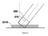
図23は、図21の拡大図である。この拡大図では、単一のエミッタと検出器との間の光路の光照射野2310が示されている。この断面図において、スタイラス先端270は、光照射野2310の一部を遮る。これは、検出器によって記録される光信号の減衰および対応する透過値の低下として見られるものとなる。図23では、スタイラス先端の側面輪郭(すなわち、y軸に沿って見たスタイラス先端の輪郭)によって遮られる光照射野の面積は約10%である。 FIG. 23 is an enlarged view of FIG. In this enlarged view, a
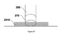
図24は、図23と同様であるが、x軸に沿った方向から見た図22の拡大図である。この方向では、スタイラス先端270の丸みを帯びた輪郭が見られる。この断面において、スタイラス先端270は、光照射野2410のより大きな部分を遮る。図24では、スタイラス先端の側面輪郭(すなわち、y軸に沿って見たスタイラス先端の輪郭)によって遮られる光照射野2410の面積は、約25%である。 24 is an enlarged view of FIG. 22, similar to FIG. 23, but viewed from the direction along the x-axis. In this direction, a rounded outline of the
図25は、タッチ面20に当てられるスタイラス先端270の平面図である。検出ラインL1、L2、L3は、タッチ面20とスタイラス先端270との間の接触点と交差する検出ライン50のサブセットであり、よってスタイラスにより減衰される。垂直線251に対する検出ラインのこの角度をファイと定義する。角度A1、A2、A3はそれぞれ、垂直線251に対する検出ラインL1、L2、L3の角度である。 FIG. 25 is a plan view of the
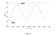
多数のエミッタおよび検出器を有するシステムでは、多くの検出ラインがスタイラス先端270と交差する可能性が高い。図26は、光路の角度ファイに対する、図21のスタイラス先端が交差する異なる光路の透過値を示すグラフである。最小値2610および最大値2620は、ファイの全範囲を横切るスタイラス先端によって生じる最小および最大透過値を示している。スタイラス先端270の場合、最小透過値は、図24に示す光路2410に対応する可能性が高く、最大透過値は、図23に示す光路2310において、特に光路がファイで約90度の角距離を有する場合に生じる可能性が高い。光路の最小透過値と最大透過値との間の比率を測定することによって、タッチ面の法線からのスタイラスの角度を判定することができる。その比率が大きいほど、スタイラスの法線からの傾きが大きくなる。比率が1:1に近いほど、スタイラスの軸がタッチ面の法線に近くなる。 In systems with multiple emitters and detectors, many detection lines are likely to intersect the
このため、本発明の好ましい実施形態では、信号プロセッサ130が、スタイラスと交差する光路の最小減衰量と最大減衰量との比率に応じて、タッチ面の法線に対するスタイラスの軸の角度を判定するように構成されている。 Thus, in a preferred embodiment of the present invention, the
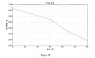
図28は、図2に係る実施形態のタッチ面に当たる角度に対するスタイラス先端270の減衰の測定値の一例を示すグラフである。タッチ面の法線に対する角度が増加するに連れて、減衰値は減少する。既知のスタイラス先端(図23に示すものなど)については、スタイラス先端の減衰値が与えられたグラフから、タッチ面の法線からのスタイラスの軸の角度を求めることができる。 FIG. 28 is a graph showing an example of measured attenuation values of the
さらに、最小および最大透過値を有する検出ラインのファイ角度が識別されると、スタイラスがファイ平面内で指し示す方向を判定することが可能である。図24に示す輪郭が、最大減衰値および最低透過値2610の原因となる可能性が高いため、スタイラスは、タッチ面の法線から所定の角度で、かつ光路2410と同じ方向に又はそれに対して180度の方向を指し示している可能性が高いと判定することができる。図26の最小透過値はファイで90度(および270度)に位置し、最大値は180度(および0度)に位置する。従って、スタイラスは、最小透過値と最大透過値との比率によって決定される角度で、かつ(図20のように)ファイ平面において90度または270度の角度で、タッチ面の法線から傾けられていると判定することができる。 Further, once the phi angle of the detection line having the minimum and maximum transmission values is identified, the direction in which the stylus points in the phi plane can be determined. Since the contour shown in FIG. 24 is likely to cause the maximum attenuation value and the
図27では、図26の最小透過値が60度(および240度)に位置し、最大透過値が150度(および330度)に位置する。したがって、スタイラスは、ファイ平面内で60度または240度の方向に傾いていると判定することができる。よって、本発明の好ましい実施形態は、最小の減衰量を有する光路のファイ値と、最大の減衰量を有する光路のファイ値との関数として、ファイ平面におけるスタイラスの傾く方向を判定することを提供する。代替的な実施形態では、最大減衰量を有する光路のファイ値のみを用いて、ファイ平面におけるスタイラスの傾く方向を判定する。 In FIG. 27, the minimum transmission value of FIG. 26 is located at 60 degrees (and 240 degrees), and the maximum transmission value is located at 150 degrees (and 330 degrees). Therefore, it can be determined that the stylus is inclined in the direction of 60 degrees or 240 degrees in the phi plane. Thus, a preferred embodiment of the present invention provides determining the direction of stylus tilt in the phi plane as a function of the phi value of the optical path having the minimum attenuation and the phi value of the optical path having the maximum attenuation. To do. In an alternative embodiment, only the phi value of the optical path with the maximum attenuation is used to determine the direction in which the stylus tilts in the phi plane.
一実施形態では、左手のユーザと右手のユーザとの間の典型的なスタイラスの傾く方向の違いにより、ユーザの左利きまたは右利きに関する情報が、傾く方向を判定するために、どのファイ値を使用するかを選択するために使用される。例えば、図26では、信号プロセッサ130は、スタイラスが、右利きのユーザについては90度のファイ、左利きのユーザの場合は270度の方向に向けられていることを判定するように構成される。 In one embodiment, due to the difference in typical stylus tilt direction between left-handed and right-handed users, the user's left-handed or right-handed information uses which phi value to determine the tilting direction. Used to select what to do. For example, in FIG. 26, the
一実施形態では、信号プロセッサ130は、最小透過値と最大透過値との比率が高いまま減衰値が再び増加し始めた場合に、タッチ面の法線に対するスタイラスの傾く角度が閾値を超えたと判定するように構成されている。そのような信号出力は、スタイラスのケーシングの一部が光照射野に入って減衰値に影響を与えているような角度で、スタイラスがタッチ面の法線に対して傾いていることによって引き起こされる可能性が高い。図29は、そのようなシナリオにおけるスタイラスの角度に対する減衰のグラフを示している。図30は、スタイラス360のケーシング380が光照射野3010に入り、減衰値を増加させることを示している。 In one embodiment, the
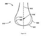
タッチ面20に接触する物体は、図31a−図31cに示すように、球形部分410を含む遠位のスタイラス先端400を有するスタイラス60であってもよい。球形部分410を有することにより、スタイラス60が傾いているときの光照射野における減衰を実質的に一定に保つことができる。これは、スタイラスが傾いたときに変化しない遠位スタイラス先端400の球形の対称性に起因する。これにより、様々な角度に傾けられたときに物体の有効幅を可能な限り一定に保つことができ、同時に使用される複数の物体を区別し易くなる。例えば、各スタイラス先端の寸法が、タッチ面上で使用されるときに、様々な描画ツールおよび色彩など特定のスタイラス特性に関連付けられる場合には、複数の異なるスタイラス60を同時に使用することができる。球形部分410は、球体410をスタイラス60の残りの部分に接続する細い遠位延長部411に配置される球体であってもよい。遠位延長部411の断面寸法を縮小することによって、光照射野内の遠位延長部411の面積が最小化されるため、スタイラス60を傾けたとき、特に大きな角度でスタイラスを傾けたときの減衰が最小化されることとなる。 The object in contact with the
図31cは、異なる高さhmaxおよびh’maxを有する2つの異なる光照射野3020,3030をそれぞれ示している。光照射野の高さが、光照射野3030のように、球形部分410よりも高い場合、減衰を増加させるために液滴形状のスタイラス先端600を有することが有利であることがある。図32a−図32cは、物体の長手方向軸612に沿って、遠位スタイラス先端600と反対の物体60の近位端611に向かって先細になる、液滴形状610,620を含む遠位スタイラス先端600を有する物体60を示している。液滴形状は、スタイラス60の近位端611に向かって長手方向612に徐々に狭まる。図32cは、高い光照射野3030における遠位先端400,600の異なる断面を示している。液滴形状の先端610は、球形部分410と比較して光照射野の上部により大きな領域を加え、それにより減衰が増大する。液滴形状610は、スタイラス60を傾けたときに、同時に有効幅の増加を最小に抑える。FIG. 31c shows two
図33aおよび図33bは、別の液滴形状のスタイラス先端600を示している。液滴形状は、少なくとも部分的な球面613を含むことができる。少なくとも部分的な球面613は、物体の長手方向軸612と交差して、その周りに回転対称性を有する遠位ベース部分621を含むことができる。少なくとも部分的な球面613は、遠位ベース部分621の近位側に配置された環状側面622をさらに備え、環状側面が、物体の長手方向軸612の周りに部分的な球面613の最大円周を規定する。環状側面622は、物体の長手方向軸612の周りに回転対称性を有する。遠位ベース部分621は、物体の長手方向軸612に平行な平面内にある円の仮想円中心に対して、環状側面622よりも大きな曲率半径を有する。遠位ベース部分621は、側面622よりも大きな曲率半径を有し、すなわち、遠位先端600の質量中心点616に向けてより平らであるか、またはより凸状ではないため、遠位先端600のボリュームの一部が、遠位先端600を傾けたときに光照射野の上方の位置にシフトすることとなる。これは図34に概略的に示されており、より小さな曲率半径を有する遠位ベース部分を有する遠位先端610と比較したとき、シフトしたボリュームの部分が614,614’として示されている。シフトしたボリューム614,614’は、その代わりに、615で光照射野の上に配置される。したがって、これは、スタイラスを傾けたときに光照射野に入る近位部分の追加されたボリュームを補正する。よって、液滴形状620は、物体の有効幅を可能な限り一定に保ちながらも、高い光照射野における機能性を改善するものとなる。 FIGS. 33a and 33b show another drop-shaped
Claims (27)
Translated fromJapaneseタッチ面(20)と、
前記タッチ面(20)の周縁の周りに配置されたエミッタのセットであって、前記タッチ面(20)に接触する物体(60)が光の減衰を生じさせるように光のビームを発するエミッタ(30a)のセットと、
前記タッチ面(20)の周縁の周りに配置されて、複数の光路上のエミッタ(30a)のセットから光を受信する光検出器(30b)のセットであって、各光検出器が、複数のエミッタ(30a)から光を受信するようにそれぞれ配置された、光検出器(30b)のセットと、
信号プロセッサ(130)であって、
前記光検出器(30b)の出力信号に基づいて、各光路の光エネルギー値を測定し、
前記光エネルギー値に基づいて各光路の透過値を生成し、
生成した透過値の少なくとも一部に対して画像再構成アルゴリズムを作動させて、
−前記タッチ面(20)上の物体(60)の位置と、
−物体(60)が前記タッチ面(20)に接触することに起因する光の減衰に対応する減衰値とを求め、
前記減衰値に応じて物体(60)の種類を判定する、
ように構成された信号プロセッサとを備えることを特徴とするタッチ検知装置。A touch detection device,
A touch surface (20);
A set of emitters arranged around the periphery of the touch surface (20), wherein the object (60) in contact with the touch surface (20) emits a beam of light so as to cause light attenuation; 30a), and
A set of photodetectors (30b) disposed around the periphery of the touch surface (20) and receiving light from a set of emitters (30a) on a plurality of optical paths, wherein each photodetector is a plurality A set of photodetectors (30b), each arranged to receive light from a plurality of emitters (30a);
A signal processor (130), comprising:
Based on the output signal of the photodetector (30b), the optical energy value of each optical path is measured,
Generating a transmission value for each optical path based on the light energy value;
Run the image reconstruction algorithm on at least some of the generated transmission values,
The position of the object (60) on the touch surface (20);
Determining an attenuation value corresponding to the attenuation of light due to the object (60) contacting the touch surface (20);
The type of the object (60) is determined according to the attenuation value.
And a signal processor configured as described above.
前記画像再構成アルゴリズムが、透過断層撮影用のアルゴリズムであることを特徴とするタッチ検知装置。The touch detection device according to claim 1,
The touch detection apparatus, wherein the image reconstruction algorithm is an algorithm for transmission tomography.
前記タッチ面(20)および反対面を規定する光透過性パネル(10)をさらに備え、前記エミッタ(30a)が、前記タッチ面と前記反対面との間の内部反射による伝播のために前記パネル内に光を導入するように構成され、前記検出器(30b)が、前記パネル内を伝播する光を受信するように構成されていることを特徴とするタッチ検知装置。The touch detection device according to claim 1 or 2,
A light transmissive panel (10) defining the touch surface (20) and the opposite surface, wherein the emitter (30a) is adapted to propagate by internal reflection between the touch surface and the opposite surface; A touch detection device configured to introduce light into the detector, wherein the detector (30b) is configured to receive light propagating through the panel.
前記エミッタ(30a)が、前記タッチ面(20)の上方に光のビームを送信するように構成され、前記検出器(30b)が、前記タッチ面(20)の上方を進行する光のビームを受信するように構成されていることを特徴とするタッチ検知装置。The touch detection device according to claim 1 or 2,
The emitter (30a) is configured to transmit a beam of light above the touch surface (20), and the detector (30b) transmits a beam of light traveling above the touch surface (20). A touch detection device configured to receive.
前記減衰値に応じて、物体(60)とタッチ面(1)との間の相互作用領域の判定が行われることを特徴とするタッチ検知装置。In the touch detection device according to any one of claims 1 to 4,
The touch detection device according to claim 1, wherein the interaction area between the object (60) and the touch surface (1) is determined according to the attenuation value.
前記エミッタ(30a)により送信されて前記検出器(30b)により受信された光のビームが、前記タッチ面(20)から5mm以内に延在していることを特徴とするタッチ検知装置。The touch detection device according to claim 4,
A touch detection device, wherein a beam of light transmitted by the emitter (30a) and received by the detector (30b) extends within 5 mm from the touch surface (20).
前記信号プロセッサ(130)がさらに、複数の物体IDを記憶するように構成され、各物体IDが、関連する減衰値の範囲を有することを特徴とするタッチ検知装置。In the touch detection apparatus according to any one of claims 1 to 6,
The touch sensing device, wherein the signal processor (130) is further configured to store a plurality of object IDs, each object ID having a range of associated attenuation values.
前記信号プロセッサ(130)がさらに、物体の減衰値に対応する減衰値の範囲を有する物体IDを識別し、物体IDを物体に関連付けるように構成されていることを特徴とするタッチ検知装置。The touch detection device according to claim 7,
The touch sensing device, wherein the signal processor (130) is further configured to identify an object ID having a range of attenuation values corresponding to the attenuation value of the object and associate the object ID with the object.
識別するステップが、前記減衰値が安定していると判定されるまで、前記信号プロセッサ(130)によって実行されないことを特徴とするタッチ検知装置。The touch detection device according to claim 8,
A touch sensing device, wherein the step of identifying is not performed by the signal processor (130) until it is determined that the attenuation value is stable.
前記減衰値の変化率が所定の閾値を下回ったときに、前記減衰値が安定していると判定されることを特徴とするタッチ検知装置。The touch detection device according to claim 9,
When the rate of change of the attenuation value falls below a predetermined threshold, it is determined that the attenuation value is stable.
前記減衰値の変化率が第1の閾値を超えて上昇したと判定された後に、前記第1の閾値よりも低い第2の閾値以下に低下した場合に、前記減衰値が安定していると判定されることを特徴とするタッチ検知装置。The touch detection device according to claim 9,
When it is determined that the rate of change of the attenuation value has risen beyond the first threshold and then falls below a second threshold that is lower than the first threshold, the attenuation value is stable. A touch detection device characterized by being determined.
前記減衰値が、物体(60)が前記タッチ面(20)に触れることによって生じる光の減衰と補正値とに応じて生成されることを特徴とするタッチ検知装置。The touch detection device according to any one of claims 1 to 11,
The touch detection device according to claim 1, wherein the attenuation value is generated according to attenuation and correction value of light generated when the object (60) touches the touch surface (20).
前記補正値が、前記タッチ面(20)上の物体(60)の少なくとも位置の関数であることを特徴とするタッチ検知装置。The touch detection device according to claim 12,
The touch detection device, wherein the correction value is a function of at least the position of the object (60) on the touch surface (20).
前記補正値が、前記タッチ面(20)上の物体(60)の位置に対応する補正マップ上の位置における値であることを特徴とするタッチ検知装置。The touch detection device according to claim 12,
The touch detection device according to claim 1, wherein the correction value is a value at a position on a correction map corresponding to the position of the object (60) on the touch surface (20).
物体(60)が物体軸を有し、前記補正値が、前記タッチ面(20)の法線に対する物体軸の少なくとも角度の関数であることを特徴とするタッチ検知装置。The touch detection device according to claim 12,
The touch detection device, wherein the object (60) has an object axis, and the correction value is a function of at least an angle of the object axis with respect to a normal line of the touch surface (20).
物体(60)が平らな先端を有し、前記タッチ面(20)の法線に対する物体軸の角度が、前記透過値と、物体(60)と交差する各光路の幾何学的配置の関数として求められることを特徴とするタッチ検知装置。The touch detection device according to claim 15, wherein
The object (60) has a flat tip, and the angle of the object axis relative to the normal of the touch surface (20) is a function of the transmission value and the geometry of each optical path intersecting the object (60). What is required is a touch detection device.
前記タッチ面(20)の法線に対する物体軸の角度が、スタイラスと交差する光路についての最小減衰量と最大減衰量との比率の関数として求められることを特徴とするタッチ検知装置。The touch detection device according to claim 15, wherein
The touch detection device characterized in that the angle of the object axis with respect to the normal of the touch surface (20) is determined as a function of the ratio between the minimum attenuation and the maximum attenuation for the optical path intersecting the stylus.
前記補正値が、前記タッチ面(20)を横切る物体(60)の少なくとも速度の関数であることを特徴とするタッチ検知装置。The touch detection device according to claim 12,
The touch detection device, wherein the correction value is a function of at least the speed of the object (60) crossing the touch surface (20).
前記補正値が、前記タッチ面(20)を横切る物体(60)の速度に比例することを特徴とするタッチ検知装置。The touch detection device according to claim 18,
The touch detection device, wherein the correction value is proportional to the speed of the object (60) crossing the touch surface (20).
物体(60)が、球形部分(410)を含む遠位スタイラス先端(400)を有することを特徴とするタッチ検知装置。In the touch detection device according to any one of claims 1 to 19,
Touch sensing device, wherein the object (60) has a distal stylus tip (400) that includes a spherical portion (410).
物体(60)が、遠位スタイラス先端(600)を有し、この遠位スタイラス先端が、長手方向物体軸(612)に沿って、遠位スタイラス先端の反対側の物体の近位端(611)に向けて先細になる液滴形状(610,620)を備えることを特徴とするタッチ検知装置。In the touch detection device according to any one of claims 1 to 19,
The object (60) has a distal stylus tip (600) that is along the longitudinal object axis (612) the proximal end (611) of the object opposite the distal stylus tip. The touch detection device is provided with a droplet shape (610, 620) that is tapered toward the surface.
前記液滴形状が、少なくとも部分的な球面(613)を含み、前記少なくとも部分的な球面が、長手方向物体軸と交差してその周りに回転対称性を有する遠位ベース部分(621)と、前記遠位ベース部分の近位側に配置された環状側面(622)とを含み、前記環状側面が、長手方向物体軸の周りに部分的な球面の最大円周を規定するとともに、長手方向物体軸の周りに回転対称性を有し、前記遠位ベース部分が、長手方向物体軸に平行な平面内にある仮想円に対して、前記環状側面よりも大きな曲率半径を有することを特徴とするタッチ検知装置。The touch detection device according to claim 21, wherein
The droplet shape includes at least a partial spherical surface (613), the at least partial spherical surface intersecting a longitudinal object axis and having rotational symmetry about the distal base portion (621); An annular side surface (622) disposed proximal of the distal base portion, the annular side surface defining a maximum circumference of a partial spherical surface about a longitudinal object axis and the longitudinal object Having rotational symmetry about an axis, wherein the distal base portion has a larger radius of curvature than the annular side with respect to an imaginary circle in a plane parallel to the longitudinal object axis Touch detection device.
前記信号プロセッサが、前記補正マップにおける予め設定された補正値間の前記補正マップのxおよびy方向の補間によって前記補正マップ上の位置の補正値を求めるように構成されていることを特徴とするタッチ検知装置。The touch detection device according to claim 14,
The signal processor is configured to obtain a correction value at a position on the correction map by interpolation in the x and y directions of the correction map between preset correction values in the correction map. Touch detection device.
前記補正値が、位置のグリッド内の各位置について求められ、前記補正マップの分解能が、前記グリッドのピッチにより決定され、前記ピッチが、前記補正マップ内の位置の関数として変化することを特徴とするタッチ検知装置。The touch detection device according to claim 23, wherein
The correction value is determined for each position in a grid of positions, the resolution of the correction map is determined by the pitch of the grid, and the pitch varies as a function of the position in the correction map. Touch detection device.
前記補正値が、光照射野の深さ(hmax)の関数であることを特徴とするタッチ検知装置。The touch detection device according to claim 12,
The touch detection device, wherein the correction value is a function of the depth (hmax ) of the light irradiation field.
前記信号プロセッサが、出力信号に基づいて光照射野の深さ(hmax)を求めるように構成されていることを特徴とするタッチ検知装置。The touch detection device according to claim 25.
The touch detection device, wherein the signal processor is configured to obtain a depth (hmax ) of a light irradiation field based on an output signal.
前記タッチ検知装置が、
タッチ面(20)と、
前記タッチ面(20)の周縁の周りに配置されたエミッタのセットであって、前記タッチ面(20)に接触する物体(60)が光を減衰させるように光のビームを発するエミッタ(30a)のセットと、
前記タッチ面(20)の周縁の周りに配置されて、複数の光路上のエミッタ(30a)のセットから光を受信する光検出器(30b)のセットであって、各光検出器が、複数のエミッタ(30a)から光を受信するようにそれぞれ配置された、光検出器(30b)のセットとを備え、
前記方法が、
前記光検出器(30b)の出力信号に基づいて、各光路の光エネルギー値を測定するステップと、
前記光エネルギー値に基づいて各光路の透過値を生成するステップと、
生成した透過値の少なくとも一部に対して画像再構成アルゴリズムを作動させて、
−前記タッチ面(20)上の物体(60)の位置と、
−物体(60)が前記タッチ面(20)に接触することに起因する光の減衰に対応する減衰値とを求めるステップと、
前記減衰値に応じて物体(60)の種類を判定するステップとを含むことを特徴とする方法。A method of determining the type of an object that touches a touch surface of a touch detection device,
The touch detection device is
A touch surface (20);
A set of emitters arranged around the periphery of the touch surface (20), the emitter (30a) emitting a beam of light such that an object (60) in contact with the touch surface (20) attenuates the light And a set of
A set of photodetectors (30b) disposed around the periphery of the touch surface (20) and receiving light from a set of emitters (30a) on a plurality of optical paths, wherein each photodetector is a plurality A set of photodetectors (30b), each arranged to receive light from an emitter (30a) of
The method comprises
Measuring the optical energy value of each optical path based on the output signal of the photodetector (30b);
Generating a transmission value for each optical path based on the light energy value;
Run the image reconstruction algorithm on at least some of the generated transmission values,
The position of the object (60) on the touch surface (20);
Determining an attenuation value corresponding to the attenuation of light due to the object (60) contacting the touch surface (20);
Determining the type of the object (60) according to the attenuation value.
Applications Claiming Priority (3)
| Application Number | Priority Date | Filing Date | Title |
|---|---|---|---|
| SE1551614-9 | 2015-12-09 | ||
| SE1551614 | 2015-12-09 | ||
| PCT/SE2016/051229WO2017099657A1 (en) | 2015-12-09 | 2016-12-07 | Improved stylus identification |
Publications (1)
| Publication Number | Publication Date |
|---|---|
| JP2018536944Atrue JP2018536944A (en) | 2018-12-13 |
Family
ID=59013880
Family Applications (1)
| Application Number | Title | Priority Date | Filing Date |
|---|---|---|---|
| JP2018529270APendingJP2018536944A (en) | 2015-12-09 | 2016-12-07 | Improved stylus identification |
Country Status (6)
| Country | Link |
|---|---|
| US (2) | US10775937B2 (en) |
| EP (2) | EP4075246B1 (en) |
| JP (1) | JP2018536944A (en) |
| KR (2) | KR102400705B1 (en) |
| CN (1) | CN108369470B (en) |
| WO (1) | WO2017099657A1 (en) |
Families Citing this family (18)
| Publication number | Priority date | Publication date | Assignee | Title |
|---|---|---|---|---|
| CN110300950B (en) | 2017-02-06 | 2023-06-16 | 平蛙实验室股份公司 | Optical coupling in touch sensing systems |
| EP4036697A1 (en) | 2017-03-28 | 2022-08-03 | FlatFrog Laboratories AB | Optical touch sensing apparatus |
| US11256371B2 (en) | 2017-09-01 | 2022-02-22 | Flatfrog Laboratories Ab | Optical component |
| JP2021028733A (en)* | 2017-12-14 | 2021-02-25 | 国立研究開発法人産業技術総合研究所 | Object identification device and object identification system |
| WO2019172826A1 (en) | 2018-03-05 | 2019-09-12 | Flatfrog Laboratories Ab | Improved touch-sensing apparatus |
| CN108762653B (en)* | 2018-04-26 | 2020-10-30 | 北京集创北方科技股份有限公司 | Touch positioning method and device and electronic equipment |
| TWI691875B (en)* | 2018-09-07 | 2020-04-21 | 友達光電股份有限公司 | Detection-display device and display module using the same |
| WO2020080992A1 (en) | 2018-10-20 | 2020-04-23 | Flatfrog Laboratories Ab | Frame for a touch-sensitive device and tool therefor |
| CN109612398B (en)* | 2018-12-07 | 2021-10-08 | 佳格科技(浙江)股份有限公司 | Touch screen object off-screen detection method |
| WO2020153890A1 (en) | 2019-01-25 | 2020-07-30 | Flatfrog Laboratories Ab | A videoconferencing terminal and method of operating the same |
| CN113424034B (en)* | 2019-02-15 | 2023-06-16 | 株式会社村田制作所 | Tactile sensation and proximity sensor |
| CN114661169B (en)* | 2019-05-16 | 2024-08-13 | 腾讯科技(深圳)有限公司 | Vision-based touch measurement method, device, equipment and storage medium |
| ES2991658T3 (en) | 2019-11-25 | 2024-12-04 | Flatfrog Lab Ab | A touch device |
| US12282653B2 (en) | 2020-02-08 | 2025-04-22 | Flatfrog Laboratories Ab | Touch apparatus with low latency interactions |
| US11893189B2 (en) | 2020-02-10 | 2024-02-06 | Flatfrog Laboratories Ab | Touch-sensing apparatus |
| CN113157127B (en)* | 2021-02-04 | 2024-11-05 | 识瓴电子科技(南通)有限责任公司 | Methods for Smart Surface System Integration |
| US11954271B2 (en)* | 2022-03-04 | 2024-04-09 | Novatek Microelectronics Corp. | Active stylus and method performed by active stylus |
| US12189902B2 (en) | 2023-01-18 | 2025-01-07 | Apple Inc. | Photo-sensing enabled display for touch detection with customized photodiode and light emitting diode component level angular response |
Family Cites Families (648)
| Publication number | Priority date | Publication date | Assignee | Title |
|---|---|---|---|---|
| FR1452041A (en) | 1965-04-26 | 1966-02-25 | Electronique & Automatisme Sa | Communication device with an electronic calculator |
| US3440426A (en) | 1966-01-11 | 1969-04-22 | Us Navy | Solar attitude encoder |
| US3673327A (en) | 1970-11-02 | 1972-06-27 | Atomic Energy Commission | Touch actuable data input panel assembly |
| IT961146B (en) | 1971-03-12 | 1973-12-10 | Schlumberger Compteurs | DEVICE PERMITTING ME TO DETERMINE THE DIRECTION OF A BRIGHT RADIATION |
| FR2172828B1 (en) | 1972-02-23 | 1974-12-13 | Dassault Electronique | |
| DE2654464A1 (en) | 1976-12-01 | 1978-06-08 | Sick Optik Elektronik Erwin | PHOTOELECTRIC LIGHT RECEIVING ARRANGEMENT |
| US4129384A (en) | 1977-06-08 | 1978-12-12 | Batelle Memorial Institute | Optical extensometer |
| US4254333A (en) | 1978-05-31 | 1981-03-03 | Bergstroem Arne | Optoelectronic circuit element |
| US4209255A (en) | 1979-03-30 | 1980-06-24 | United Technologies Corporation | Single source aiming point locator |
| US4213707A (en) | 1979-04-25 | 1980-07-22 | Eastman Kodak Company | Device for improving the accuracy of optical measuring apparatus and the like |
| US4254407A (en) | 1979-07-18 | 1981-03-03 | Ncr Corporation | Data processing system having optically linked subsystems, including an optical keyboard |
| US4294543A (en) | 1979-11-13 | 1981-10-13 | Command Control & Communications Corporation | Optical system for developing point coordinate information |
| US4484179A (en) | 1980-04-16 | 1984-11-20 | At&T Bell Laboratories | Touch position sensitive surface |
| US4346376A (en) | 1980-04-16 | 1982-08-24 | Bell Telephone Laboratories, Incorporated | Touch position sensitive surface |
| US4420261A (en) | 1980-09-02 | 1983-12-13 | Lowbar, Inc. | Optical position location apparatus |
| JPS58111705A (en) | 1981-12-25 | 1983-07-02 | Mitsutoyo Mfg Co Ltd | Optical measuring device |
| US4459476A (en) | 1982-01-19 | 1984-07-10 | Zenith Radio Corporation | Co-ordinate detection system |
| US4542375A (en) | 1982-02-11 | 1985-09-17 | At&T Bell Laboratories | Deformable touch sensitive surface |
| GB2131544B (en) | 1982-12-07 | 1986-03-05 | Lowbar Inc | Optical postition location apparatus |
| US4593191A (en) | 1982-12-29 | 1986-06-03 | At&T Bell Laboratories | Pressure and optical sensitive device with deformable protrusions |
| GB8302997D0 (en) | 1983-02-03 | 1983-03-09 | Bergstrom A | Electromagnetic radiation circuit element |
| US4507557A (en) | 1983-04-01 | 1985-03-26 | Siemens Corporate Research & Support, Inc. | Non-contact X,Y digitizer using two dynamic ram imagers |
| US4550250A (en) | 1983-11-14 | 1985-10-29 | Hei, Inc. | Cordless digital graphics input device |
| US4752655A (en) | 1984-11-16 | 1988-06-21 | Nippon Telegraph & Telephone Corporation | Coordinate input device |
| US4692809A (en) | 1984-11-20 | 1987-09-08 | Hughes Aircraft Company | Integrated touch paint system for displays |
| US4673918A (en) | 1984-11-29 | 1987-06-16 | Zenith Electronics Corporation | Light guide having focusing element and internal reflector on same face |
| JPH0325219Y2 (en) | 1985-02-15 | 1991-05-31 | ||
| JPH0325220Y2 (en) | 1985-02-15 | 1991-05-31 | ||
| US4710760A (en) | 1985-03-07 | 1987-12-01 | American Telephone And Telegraph Company, At&T Information Systems Inc. | Photoelastic touch-sensitive screen |
| JPS61152133U (en) | 1985-03-12 | 1986-09-20 | ||
| US4688993A (en) | 1985-03-21 | 1987-08-25 | United Technologies Corporation | Tangential link swashplate centering member |
| DE3511330A1 (en) | 1985-03-28 | 1986-10-02 | Siemens Ag | Arrangement for inputting graphic patterns |
| US5073770A (en) | 1985-04-19 | 1991-12-17 | Lowbner Hugh G | Brightpen/pad II |
| US4949079A (en) | 1985-04-19 | 1990-08-14 | Hugh Loebner | Brightpen/pad graphic device for computer inputs and the like |
| US5159322A (en) | 1985-04-19 | 1992-10-27 | Loebner Hugh G | Apparatus to digitize graphic and scenic information and to determine the position of a stylus for input into a computer or the like |
| US4688933A (en) | 1985-05-10 | 1987-08-25 | The Laitram Corporation | Electro-optical position determining system |
| US4736191A (en) | 1985-08-02 | 1988-04-05 | Karl E. Matzke | Touch activated control method and apparatus |
| JPH0318997Y2 (en) | 1985-10-04 | 1991-04-22 | ||
| JPS62159213A (en) | 1986-01-07 | 1987-07-15 | Alps Electric Co Ltd | Coordinates input device |
| JPH0762821B2 (en) | 1986-05-30 | 1995-07-05 | 株式会社日立製作所 | Touch panel input device |
| US4782328A (en) | 1986-10-02 | 1988-11-01 | Product Development Services, Incorporated | Ambient-light-responsive touch screen data input method and system |
| US4891829A (en) | 1986-11-19 | 1990-01-02 | Exxon Research And Engineering Company | Method and apparatus for utilizing an electro-optic detector in a microtomography system |
| US4868912A (en) | 1986-11-26 | 1989-09-19 | Digital Electronics | Infrared touch panel |
| US4746770A (en) | 1987-02-17 | 1988-05-24 | Sensor Frame Incorporated | Method and apparatus for isolating and manipulating graphic objects on computer video monitor |
| US4820050A (en) | 1987-04-28 | 1989-04-11 | Wells-Gardner Electronics Corporation | Solid-state optical position determining apparatus |
| FR2614711B1 (en) | 1987-04-29 | 1992-03-13 | Photonetics | METHOD AND DEVICE FOR OPERATING THE SCREEN SIGNAL OF A TOUCH SCREEN |
| FR2617619B1 (en) | 1987-07-02 | 1990-01-05 | Photonetics | OPTICAL TOUCH SCREEN MOUNTING DEVICE |
| FR2617620B1 (en) | 1987-07-02 | 1992-09-25 | Photonetics | OPTICAL TYPE TOUCH SCREEN |
| US4772763A (en) | 1987-08-25 | 1988-09-20 | International Business Machines Corporation | Data processing information input using optically sensed stylus features |
| JPH01195526A (en) | 1988-01-29 | 1989-08-07 | Sony Corp | Touch panel device |
| FR2631438B1 (en) | 1988-05-11 | 1991-06-21 | Photonetics | METHOD FOR POSITIONING AN OBJECT RELATIVE TO A PLANE, METHOD FOR MEASURING LENGTH AND DEVICES FOR CARRYING OUT SAID METHODS |
| US4988983A (en) | 1988-09-02 | 1991-01-29 | Carroll Touch, Incorporated | Touch entry system with ambient compensation and programmable amplification |
| US4986662A (en) | 1988-12-19 | 1991-01-22 | Amp Incorporated | Touch entry using discrete reflectors |
| FR2645645B1 (en) | 1989-04-06 | 1991-07-12 | Photonetics | IMPROVEMENTS IN METHODS AND DEVICES FOR DETERMINING THE ANGLE OF CONTACT OF A DROP OF LIQUID PLACED ON A SUBSTRATE |
| US4916712A (en) | 1989-07-27 | 1990-04-10 | Mcdonnell Douglas Corporation | Optically pumped slab laser |
| US5065185A (en) | 1989-08-21 | 1991-11-12 | Powers Edward A | Multi-function detecting device for a document reproduction machine |
| DK0424064T3 (en) | 1989-10-16 | 1995-06-26 | Chiroscience Ltd | Chiral azabicycloheptanones and process for their preparation |
| US5105186A (en) | 1990-05-25 | 1992-04-14 | Hewlett-Packard Company | Lcd touch screen |
| US6390370B1 (en) | 1990-11-15 | 2002-05-21 | Symbol Technologies, Inc. | Light beam scanning pen, scan module for the device and method of utilization |
| US5166668A (en) | 1991-04-10 | 1992-11-24 | Data Stream Corporation | Wireless pen-type input device for use with a computer |
| FR2676275A1 (en) | 1991-05-07 | 1992-11-13 | Photonetics | DEVICE FOR REMOTELY MEASURING THE POSITION OF AN OBJECT. |
| US5539514A (en) | 1991-06-26 | 1996-07-23 | Hitachi, Ltd. | Foreign particle inspection apparatus and method with front and back illumination |
| US5345490A (en) | 1991-06-28 | 1994-09-06 | General Electric Company | Method and apparatus for converting computed tomography (CT) data into finite element models |
| US5335557A (en) | 1991-11-26 | 1994-08-09 | Taizo Yasutake | Touch sensitive input control device |
| CA2060564C (en) | 1992-02-06 | 1996-05-21 | Toru Suzuki | Wireless input system for computer |
| US5483261A (en) | 1992-02-14 | 1996-01-09 | Itu Research, Inc. | Graphical input controller and method with rear screen image detection |
| CH683370A5 (en) | 1992-04-10 | 1994-02-28 | Zumbach Electronic Ag | Method and apparatus for measuring the dimension of an object. |
| CA2068191C (en) | 1992-05-07 | 1994-11-22 | Fernand Sergerie | Reinforced composite backing tape |
| US7084859B1 (en) | 1992-09-18 | 2006-08-01 | Pryor Timothy R | Programmable tactile touch screen displays and man-machine interfaces for improved vehicle instrumentation and telematics |
| US5248856A (en) | 1992-10-07 | 1993-09-28 | Microfield Graphics, Inc. | Code-based, electromagnetic-field-responsive graphic data-acquisition system |
| CN1078351C (en) | 1992-11-25 | 2002-01-23 | 住友电气工业株式会社 | Method of detecting impurities in molten resin |
| US5502568A (en) | 1993-03-23 | 1996-03-26 | Wacom Co., Ltd. | Optical position detecting unit, optical coordinate input unit and optical position detecting method employing a pattern having a sequence of 1's and 0's |
| JP3400485B2 (en) | 1993-03-23 | 2003-04-28 | 株式会社ワコム | Optical position detecting device and optical coordinate input device |
| DE4334937A1 (en) | 1993-10-13 | 1995-10-05 | Siemens Ag | Computer tomograph |
| JP3135183B2 (en) | 1993-10-29 | 2001-02-13 | 株式会社ワコム | Position indicator |
| WO1995014286A1 (en) | 1993-11-17 | 1995-05-26 | Microsoft Corporation | Wireless pen computer input system |
| US5484966A (en) | 1993-12-07 | 1996-01-16 | At&T Corp. | Sensing stylus position using single 1-D image sensor |
| JPH07200137A (en) | 1993-12-28 | 1995-08-04 | Wacom Co Ltd | Position detection device and its position indicator |
| US5515083A (en) | 1994-02-17 | 1996-05-07 | Spacelabs Medical, Inc. | Touch screen having reduced sensitivity to spurious selections |
| JPH07261920A (en) | 1994-03-17 | 1995-10-13 | Wacom Co Ltd | Optical position detector and optical coordinate input device |
| JP3421416B2 (en) | 1994-03-18 | 2003-06-30 | 株式会社ワコム | Position detecting device and its position indicator |
| US5525764A (en) | 1994-06-09 | 1996-06-11 | Junkins; John L. | Laser scanning graphic input system |
| US5526422A (en) | 1994-06-20 | 1996-06-11 | At&T Corp. | System and method for cleaning the display screen of a touch screen device |
| DE19521254A1 (en) | 1994-06-24 | 1996-01-04 | Minnesota Mining & Mfg | Display system with brightness boosting film |
| US5740224A (en) | 1994-09-27 | 1998-04-14 | University Of Delaware | Cone beam synthetic arrays in three-dimensional computerized tomography |
| US5686942A (en) | 1994-12-01 | 1997-11-11 | National Semiconductor Corporation | Remote computer input system which detects point source on operator |
| US5736686A (en) | 1995-03-01 | 1998-04-07 | Gtco Corporation | Illumination apparatus for a digitizer tablet with improved light panel |
| US5764223A (en) | 1995-06-07 | 1998-06-09 | International Business Machines Corporation | Touch-screen input device using the monitor as a light source operating at an intermediate frequency |
| US6031524A (en) | 1995-06-07 | 2000-02-29 | Intermec Ip Corp. | Hand-held portable data terminal having removably interchangeable, washable, user-replaceable components with liquid-impervious seal |
| CA2225734C (en) | 1995-06-29 | 2006-11-14 | Lynn Wiese | Localized illumination using tir technology |
| GB9516441D0 (en) | 1995-08-10 | 1995-10-11 | Philips Electronics Uk Ltd | Light pen input systems |
| WO1997041527A1 (en) | 1996-05-01 | 1997-11-06 | Xros, Inc. | Compact, simple, 2d raster, image-building fingerprint scanner |
| PL330188A1 (en) | 1996-05-29 | 1999-04-26 | Deutsche Telekom Ag | Information entering apparatus |
| US6067079A (en) | 1996-06-13 | 2000-05-23 | International Business Machines Corporation | Virtual pointing device for touchscreens |
| DE19631414A1 (en) | 1996-08-05 | 1998-02-19 | Daimler Benz Ag | Device for recording the retinal reflex image and superimposing additional images in the eye |
| JP3300856B2 (en) | 1996-08-12 | 2002-07-08 | イーエルオー・タッチシステムズ・インコーポレイテッド | Acoustic state sensor using multiple mutually non-orthogonal waves |
| US5767517A (en) | 1996-10-21 | 1998-06-16 | Board Of Regents -Univ. Of Ne | Hybrid resampling method for fan beam spect |
| EP0845812B1 (en) | 1996-11-28 | 2009-10-28 | Casio Computer Co., Ltd. | Display apparatus |
| US6061177A (en) | 1996-12-19 | 2000-05-09 | Fujimoto; Kenneth Noboru | Integrated computer display and graphical input apparatus and method |
| WO1998036236A1 (en) | 1997-02-13 | 1998-08-20 | Super Dimension Ltd. | Six-degree tracking system |
| JPH113169A (en) | 1997-06-13 | 1999-01-06 | Tokai Rika Co Ltd | Touch operation information output device |
| US6229529B1 (en) | 1997-07-11 | 2001-05-08 | Ricoh Company, Ltd. | Write point detecting circuit to detect multiple write points |
| US6480187B1 (en) | 1997-08-07 | 2002-11-12 | Fujitsu Limited | Optical scanning-type touch panel |
| US6141104A (en) | 1997-09-09 | 2000-10-31 | Image Guided Technologies, Inc. | System for determination of a location in three dimensional space |
| US6909419B2 (en) | 1997-10-31 | 2005-06-21 | Kopin Corporation | Portable microdisplay system |
| US5945980A (en) | 1997-11-14 | 1999-08-31 | Logitech, Inc. | Touchpad with active plane for pen detection |
| KR100595922B1 (en) | 1998-01-26 | 2006-07-05 | 웨인 웨스터만 | Method and apparatus for integrating manual input |
| US9292111B2 (en) | 1998-01-26 | 2016-03-22 | Apple Inc. | Gesturing with a multipoint sensing device |
| US6315156B1 (en) | 1998-01-26 | 2001-11-13 | Gpax International, Inc. | Tape-form packaging system and apparatus for effecting assembly and disassembly thereof |
| DE19809934A1 (en) | 1998-03-07 | 1999-09-09 | Bosch Gmbh Robert | Laser display panel with contact detection |
| AU6633798A (en) | 1998-03-09 | 1999-09-27 | Gou Lite Ltd. | Optical translation measurement |
| US6172667B1 (en) | 1998-03-19 | 2001-01-09 | Michel Sayag | Optically-based touch screen input device |
| US6748098B1 (en) | 1998-04-14 | 2004-06-08 | General Electric Company | Algebraic reconstruction of images from non-equidistant data |
| JP3827450B2 (en) | 1998-08-18 | 2006-09-27 | 富士通株式会社 | Optical scanning touch panel |
| US7268774B2 (en) | 1998-08-18 | 2007-09-11 | Candledragon, Inc. | Tracking motion of a writing instrument |
| US6972753B1 (en) | 1998-10-02 | 2005-12-06 | Semiconductor Energy Laboratory Co., Ltd. | Touch panel, display device provided with touch panel and electronic equipment provided with display device |
| JP3530758B2 (en) | 1998-12-03 | 2004-05-24 | キヤノン株式会社 | Pointer for inputting coordinates |
| JP4007705B2 (en) | 1998-11-20 | 2007-11-14 | 富士通株式会社 | Optical scanning touch panel |
| US6175999B1 (en) | 1999-01-12 | 2001-01-23 | Dell Usa, L.P. | Universal fixture for pre-assembly of computer components |
| JP4245721B2 (en) | 1999-03-05 | 2009-04-02 | プラスビジョン株式会社 | Coordinate input pen |
| US6333735B1 (en) | 1999-03-16 | 2001-12-25 | International Business Machines Corporation | Method and apparatus for mouse positioning device based on infrared light sources and detectors |
| JP4097353B2 (en) | 1999-04-07 | 2008-06-11 | 富士通株式会社 | Optical scanning touch panel |
| JP4939682B2 (en) | 1999-04-27 | 2012-05-30 | エーユー オプトロニクス コーポレイション | Display device |
| DE19924448A1 (en) | 1999-05-28 | 2000-12-07 | Siemens Ag | Three-dimensional data set extraction method for magnetic resonance imaging |
| FR2794246B1 (en) | 1999-05-31 | 2001-08-10 | Saint Louis Inst | DEVICE CAPABLE OF DETERMINING THE POSITION OF AN OBJECT IN AN OXZ MARK |
| EP1188069A2 (en) | 1999-06-09 | 2002-03-20 | Beamcontrol Aps | A method for determining the channel gain between emitters and receivers |
| FR2795877B1 (en) | 1999-06-30 | 2001-10-05 | Photonetics | PARTIALLY REFLECTIVE OPTICAL COMPONENT AND LASER SOURCE INCORPORATING SUCH COMPONENT |
| US6366277B1 (en) | 1999-10-13 | 2002-04-02 | Elo Touchsystems, Inc. | Contaminant processing system for an acoustic touchscreen |
| JP3606138B2 (en) | 1999-11-05 | 2005-01-05 | セイコーエプソン株式会社 | Driver IC, electro-optical device and electronic apparatus |
| JP2001147772A (en) | 1999-11-19 | 2001-05-29 | Fujitsu Takamisawa Component Ltd | Touch panel |
| JP3780785B2 (en) | 1999-11-30 | 2006-05-31 | 三菱電機株式会社 | Concavity and convexity pattern detector |
| MXPA02005431A (en) | 1999-12-02 | 2003-02-12 | Elo Touchsystems Inc | Apparatus and method to improve resolution of infrared touch systems. |
| JP2001183987A (en) | 1999-12-27 | 2001-07-06 | Pioneer Electronic Corp | Cooling structure and display device using the same |
| US20040252867A1 (en) | 2000-01-05 | 2004-12-16 | Je-Hsiung Lan | Biometric sensor |
| JP2001209487A (en) | 2000-01-25 | 2001-08-03 | Uw:Kk | Handwriting communication system, and handwriting input and handwriting display device used for the system |
| JP3881148B2 (en) | 2000-02-18 | 2007-02-14 | 株式会社リコー | Photodetection device for coordinate detection, coordinate input / detection device, electronic blackboard, mounting position detection method, and storage medium |
| US6495832B1 (en) | 2000-03-15 | 2002-12-17 | Touch Controls, Inc. | Photoelectric sensing array apparatus and method of using same |
| WO2001078052A1 (en) | 2000-04-05 | 2001-10-18 | Dimensional Media Associates, Inc. | Methods and apparatus for virtual touchscreen computer interface controller |
| US7859519B2 (en) | 2000-05-01 | 2010-12-28 | Tulbert David J | Human-machine interface |
| US6864882B2 (en) | 2000-05-24 | 2005-03-08 | Next Holdings Limited | Protected touch panel display system |
| US6690363B2 (en) | 2000-06-19 | 2004-02-10 | Next Holdings Limited | Touch panel display system |
| US6724489B2 (en) | 2000-09-22 | 2004-04-20 | Daniel Freifeld | Three dimensional scanning camera |
| US6660964B1 (en) | 2000-09-22 | 2003-12-09 | David Benderly | Optical modification of laser beam cross section in object marking systems |
| JP2004534974A (en) | 2000-10-27 | 2004-11-18 | エロ・タッチシステムズ・インコーポレイテッド | Touch confirmation type touch screen using multiple touch sensors |
| CN1227617C (en) | 2000-11-06 | 2005-11-16 | 皇家菲利浦电子有限公司 | Method of measuring movement of input device |
| US6648485B1 (en) | 2000-11-13 | 2003-11-18 | International Business Machines Corporation | Highly collimating tapered light guide for uniform illumination of flat panel displays |
| ATE395866T1 (en) | 2000-12-30 | 2008-06-15 | Univ Leeds | ELECTRICAL IMPEDANCE TOMOGRAPHY |
| JP4004025B2 (en) | 2001-02-13 | 2007-11-07 | 日東電工株式会社 | Transparent conductive laminate and touch panel |
| DE10110744A1 (en) | 2001-03-07 | 2002-09-26 | Franc Godler | Large, touch-sensitive area with time and location-controlled transmitter and receiver modules |
| US6452996B1 (en) | 2001-03-16 | 2002-09-17 | Ge Medical Systems Global Technology Company, Llc | Methods and apparatus utilizing generalized helical interpolation algorithm |
| JP4768143B2 (en) | 2001-03-26 | 2011-09-07 | 株式会社リコー | Information input / output device, information input / output control method, and program |
| US6738051B2 (en) | 2001-04-06 | 2004-05-18 | 3M Innovative Properties Company | Frontlit illuminated touch panel |
| JP4812181B2 (en) | 2001-04-20 | 2011-11-09 | オリンパス株式会社 | Observation optical system, imaging optical system, and apparatus using the same |
| US6992659B2 (en) | 2001-05-22 | 2006-01-31 | Palmone, Inc. | High transparency integrated enclosure touch screen assembly for a portable hand held device |
| JP3959678B2 (en) | 2001-07-13 | 2007-08-15 | ミネベア株式会社 | Touch panel for display device |
| DE10136611C1 (en) | 2001-07-23 | 2002-11-21 | Jenoptik Laserdiode Gmbh | Optical device, for laser light emitted by laser diode device, has collimation optical element and homogenizing element using multiple reflection of laser beam |
| US6927384B2 (en) | 2001-08-13 | 2005-08-09 | Nokia Mobile Phones Ltd. | Method and device for detecting touch pad unit |
| US6985137B2 (en) | 2001-08-13 | 2006-01-10 | Nokia Mobile Phones Ltd. | Method for preventing unintended touch pad input due to accidental touching |
| US6765193B2 (en) | 2001-08-21 | 2004-07-20 | National Science And Technology Development Agency | Optical touch switch structures |
| US20030048257A1 (en) | 2001-09-06 | 2003-03-13 | Nokia Mobile Phones Ltd. | Telephone set having a touch pad device |
| US7254775B2 (en) | 2001-10-03 | 2007-08-07 | 3M Innovative Properties Company | Touch panel system and method for distinguishing multiple touch inputs |
| JP2005505075A (en) | 2001-10-09 | 2005-02-17 | コーニンクレッカ フィリップス エレクトロニクス エヌ ヴィ | Device having touch sensitivity function |
| US20120188206A1 (en) | 2001-11-02 | 2012-07-26 | Neonode, Inc. | Optical touch screen with tri-directional micro-lenses |
| US20100238139A1 (en) | 2009-02-15 | 2010-09-23 | Neonode Inc. | Optical touch screen systems using wide light beams |
| US9471170B2 (en) | 2002-11-04 | 2016-10-18 | Neonode Inc. | Light-based touch screen with shift-aligned emitter and receiver lenses |
| US8339379B2 (en) | 2004-04-29 | 2012-12-25 | Neonode Inc. | Light-based touch screen |
| US6948840B2 (en) | 2001-11-16 | 2005-09-27 | Everbrite, Llc | Light emitting diode light bar |
| US6664498B2 (en) | 2001-12-04 | 2003-12-16 | General Atomics | Method and apparatus for increasing the material removal rate in laser machining |
| KR100449710B1 (en) | 2001-12-10 | 2004-09-22 | 삼성전자주식회사 | Remote pointing method and apparatus therefor |
| US7006080B2 (en) | 2002-02-19 | 2006-02-28 | Palm, Inc. | Display system |
| JP4477811B2 (en) | 2002-02-27 | 2010-06-09 | Hoya株式会社 | Mounting plate for solid-state image sensor and mounting method to the mounting plate |
| CN100511115C (en) | 2002-03-13 | 2009-07-08 | 平蛙实验室股份公司 | A touch pad, a stylus for use with the touch pad, and a method of operating the touch pad |
| DE10211307A1 (en) | 2002-03-13 | 2003-11-20 | Mechaless Systems Gmbh | Device and method for optoelectronic detection of the movement and / or position of an object |
| WO2003083767A2 (en) | 2002-03-27 | 2003-10-09 | Nellcor Puritan Bennett Incorporated | Infrared touchframe system |
| US20040134772A1 (en) | 2002-10-01 | 2004-07-15 | Microfabrica Inc. | Monolithic structures including alignment and/or retention fixtures for accepting components |
| DE50308334D1 (en) | 2002-05-07 | 2007-11-22 | Schott Ag | Lighting device for buttons |
| JP2003330603A (en) | 2002-05-13 | 2003-11-21 | Ricoh Co Ltd | Coordinate detecting device, coordinate detecting method, coordinate detecting program for causing a computer to execute the method, and recording medium storing the coordinate detecting program |
| US7176897B2 (en) | 2002-05-17 | 2007-02-13 | 3M Innovative Properties Company | Correction of memory effect errors in force-based touch panel systems |
| US7952570B2 (en) | 2002-06-08 | 2011-05-31 | Power2B, Inc. | Computer navigation |
| US20090143141A1 (en) | 2002-08-06 | 2009-06-04 | Igt | Intelligent Multiplayer Gaming System With Multi-Touch Display |
| US7151532B2 (en) | 2002-08-09 | 2006-12-19 | 3M Innovative Properties Company | Multifunctional multilayer optical film |
| JP2004078613A (en) | 2002-08-19 | 2004-03-11 | Fujitsu Ltd | Touch panel device |
| US7133031B2 (en) | 2002-10-31 | 2006-11-07 | Microsoft Corporation | Optical system design for a universal computing device |
| JP4093308B2 (en) | 2002-11-01 | 2008-06-04 | 富士通株式会社 | Touch panel device and contact position detection method |
| US8587562B2 (en) | 2002-11-04 | 2013-11-19 | Neonode Inc. | Light-based touch screen using elliptical and parabolic reflectors |
| US9389730B2 (en)* | 2002-12-10 | 2016-07-12 | Neonode Inc. | Light-based touch screen using elongated light guides |
| US8902196B2 (en) | 2002-12-10 | 2014-12-02 | Neonode Inc. | Methods for determining a touch location on a touch screen |
| US7042444B2 (en) | 2003-01-17 | 2006-05-09 | Eastman Kodak Company | OLED display and touch screen |
| US7629967B2 (en) | 2003-02-14 | 2009-12-08 | Next Holdings Limited | Touch screen signal processing |
| US7532206B2 (en) | 2003-03-11 | 2009-05-12 | Smart Technologies Ulc | System and method for differentiating between pointers used to contact touch surface |
| EP1604271A2 (en) | 2003-03-12 | 2005-12-14 | O-Pen ApS | A multitasking radiation sensor |
| WO2004081502A2 (en) | 2003-03-12 | 2004-09-23 | O-Pen Aps | A system and a method of determining the position of a radiation emitting element |
| KR100533839B1 (en) | 2003-03-14 | 2005-12-07 | 삼성전자주식회사 | Control device of electronic devices based on motion |
| EP1616288A4 (en) | 2003-04-07 | 2008-02-27 | Silverbrook Res Pty Ltd | LASER SCANNING DEVICE FOR PRINTING PRODUCT IDENTIFICATION CODES |
| US7786983B2 (en) | 2003-04-08 | 2010-08-31 | Poa Sana Liquidating Trust | Apparatus and method for a data input device using a light lamina screen |
| US7133032B2 (en) | 2003-04-24 | 2006-11-07 | Eastman Kodak Company | OLED display and touch screen |
| US7362320B2 (en) | 2003-06-05 | 2008-04-22 | Hewlett-Packard Development Company, L.P. | Electronic device having a light emitting/detecting display screen |
| JP2005004278A (en) | 2003-06-09 | 2005-01-06 | Ricoh Elemex Corp | Coordinate input device |
| US7432893B2 (en) | 2003-06-14 | 2008-10-07 | Massachusetts Institute Of Technology | Input device based on frustrated total internal reflection |
| US7474772B2 (en) | 2003-06-25 | 2009-01-06 | Atrua Technologies, Inc. | System and method for a miniature user input device |
| JP4405766B2 (en) | 2003-08-07 | 2010-01-27 | キヤノン株式会社 | Coordinate input device, coordinate input method |
| WO2005022194A2 (en) | 2003-08-13 | 2005-03-10 | Lettvin Jonathan D | Imaging system |
| US7359041B2 (en) | 2003-09-04 | 2008-04-15 | Avago Technologies Ecbu Ip Pte Ltd | Method and system for optically tracking a target using a triangulation technique |
| US7442914B2 (en) | 2003-09-12 | 2008-10-28 | Flatfrog Laboratories Ab | System and method of determining a position of a radiation emitting element |
| ATE514991T1 (en) | 2003-09-12 | 2011-07-15 | Flatfrog Lab Ab | SYSTEM AND METHOD FOR DETERMINING A POSITION OF A RADIATION SCATTERING/REFLECTION ELEMENT |
| KR100534968B1 (en) | 2003-09-16 | 2005-12-08 | 현대자동차주식회사 | cooling structure of an electronic element |
| WO2005029172A2 (en) | 2003-09-22 | 2005-03-31 | Koninklijke Philips Electronics N.V. | Touch input screen using a light guide |
| JP2007506180A (en) | 2003-09-22 | 2007-03-15 | コニンクリユケ フィリップス エレクトロニクス エヌ.ブイ. | Coordinate detection system for display monitor |
| US9123077B2 (en) | 2003-10-07 | 2015-09-01 | Hospira, Inc. | Medication management system |
| US7221374B2 (en) | 2003-10-21 | 2007-05-22 | Hewlett-Packard Development Company, L.P. | Adjustment of color in displayed images based on identification of ambient light sources |
| JP2005165199A (en) | 2003-12-05 | 2005-06-23 | Alps Electric Co Ltd | Prism sheet, lighting device, surface emitting apparatus, and liquid crystal display device |
| EP1704752A4 (en) | 2003-12-11 | 2009-09-23 | Philips Solid State Lighting | Thermal management methods and apparatus for lighting devices |
| US7265748B2 (en) | 2003-12-11 | 2007-09-04 | Nokia Corporation | Method and device for detecting touch pad input |
| GB2409304B (en) | 2003-12-19 | 2007-11-14 | Westerngeco Ltd | Processing geophysical data |
| JP4616559B2 (en) | 2004-01-15 | 2011-01-19 | 大日本印刷株式会社 | Display device and display system |
| US7087907B1 (en) | 2004-02-02 | 2006-08-08 | Advanced Micro Devices, Inc. | Detection of contamination in imaging systems by fluorescence and/or absorption spectroscopy |
| US7342705B2 (en) | 2004-02-03 | 2008-03-11 | Idc, Llc | Spatial light modulator with integrated optical compensation structure |
| JP4522113B2 (en) | 2004-03-11 | 2010-08-11 | キヤノン株式会社 | Coordinate input device |
| US20060033725A1 (en) | 2004-06-03 | 2006-02-16 | Leapfrog Enterprises, Inc. | User created interactive interface |
| US7310090B2 (en) | 2004-03-25 | 2007-12-18 | Avago Technologies Ecbm Ip (Singapore) Pte Ltd. | Optical generic switch panel |
| US6965836B2 (en) | 2004-04-19 | 2005-11-15 | Battelle Energy Alliance, Llc | Method and apparatus for two dimensional surface property analysis based on boundary measurement |
| US7538759B2 (en) | 2004-05-07 | 2009-05-26 | Next Holdings Limited | Touch panel display system with illumination and detection provided from a single edge |
| EP1794740A4 (en) | 2004-05-11 | 2012-01-25 | Motion Computing Inc | Improved display for stylus input displays |
| JP4429083B2 (en) | 2004-06-03 | 2010-03-10 | キヤノン株式会社 | Shading type coordinate input device and coordinate input method thereof |
| GB0413747D0 (en) | 2004-06-19 | 2004-07-21 | Atomic Energy Authority Uk | Optical keyboard |
| US8184108B2 (en) | 2004-06-30 | 2012-05-22 | Poa Sana Liquidating Trust | Apparatus and method for a folded optical element waveguide for use with light based touch screens |
| US7743348B2 (en) | 2004-06-30 | 2010-06-22 | Microsoft Corporation | Using physical objects to adjust attributes of an interactive display application |
| US7565020B2 (en) | 2004-07-03 | 2009-07-21 | Microsoft Corp. | System and method for image coding employing a hybrid directional prediction and wavelet lifting |
| ES2555309T3 (en) | 2004-07-06 | 2015-12-30 | Maricare Oy | Sensor product for electric field detection |
| JP2006039686A (en) | 2004-07-22 | 2006-02-09 | Pioneer Electronic Corp | Touch panel device, touch region detecting method, and touch region detecting program |
| US7653883B2 (en) | 2004-07-30 | 2010-01-26 | Apple Inc. | Proximity detector in handheld device |
| US20060038698A1 (en) | 2004-08-19 | 2006-02-23 | Chen Jim T | Multi-purpose remote control input device |
| JP4761736B2 (en) | 2004-08-20 | 2011-08-31 | 東芝モバイルディスプレイ株式会社 | Liquid crystal display |
| US20060061861A1 (en) | 2004-09-23 | 2006-03-23 | Reflexite Corporation | High performance rear-projection screen |
| US20060066586A1 (en) | 2004-09-27 | 2006-03-30 | Gally Brian J | Touchscreens for displays |
| US7702142B2 (en) | 2004-11-15 | 2010-04-20 | Hologic, Inc. | Matching geometry generation and display of mammograms and tomosynthesis images |
| US8599140B2 (en) | 2004-11-17 | 2013-12-03 | International Business Machines Corporation | Providing a frustrated total internal reflection touch interface |
| US7847789B2 (en) | 2004-11-23 | 2010-12-07 | Microsoft Corporation | Reducing accidental touch-sensitive device activation |
| US20060132454A1 (en) | 2004-12-16 | 2006-06-22 | Deng-Peng Chen | Systems and methods for high resolution optical touch position systems |
| US20060158437A1 (en) | 2005-01-20 | 2006-07-20 | Blythe Michael M | Display device |
| US7800594B2 (en) | 2005-02-03 | 2010-09-21 | Toshiba Matsushita Display Technology Co., Ltd. | Display device including function to input information from screen by light |
| US8298078B2 (en) | 2005-02-28 | 2012-10-30 | Wms Gaming Inc. | Wagering game machine with biofeedback-aware game presentation |
| US20060202974A1 (en) | 2005-03-10 | 2006-09-14 | Jeffrey Thielman | Surface |
| KR20070116870A (en)* | 2005-03-10 | 2007-12-11 | 코닌클리케 필립스 일렉트로닉스 엔.브이. | System and method for detecting the position, size and shape of multiple objects interacting with a touch screen display |
| US7705835B2 (en) | 2005-03-28 | 2010-04-27 | Adam Eikman | Photonic touch screen apparatus and method of use |
| US7840625B2 (en) | 2005-04-07 | 2010-11-23 | California Institute Of Technology | Methods for performing fast discrete curvelet transforms of data |
| JP2008545183A (en) | 2005-05-12 | 2008-12-11 | サーク・コーポレーション | Reconfigurable interactive interface device including an optical display using an airgel to direct light in a desired direction and an optical touchpad |
| US7646833B1 (en) | 2005-05-23 | 2010-01-12 | Marvell International Ltd. | Channel equalization in receivers |
| EP1907918A2 (en) | 2005-07-05 | 2008-04-09 | O-Pen ApS | A touch pad system |
| US7916144B2 (en) | 2005-07-13 | 2011-03-29 | Siemens Medical Solutions Usa, Inc. | High speed image reconstruction for k-space trajectory data using graphic processing unit (GPU) |
| US7629968B2 (en) | 2005-07-29 | 2009-12-08 | Avago Technologies Fiber Ip (Singapore) Pte. Ltd. | Methods and systems for detecting selections on a touch screen display |
| US7737959B2 (en) | 2005-09-08 | 2010-06-15 | Avago Technologies Ecbu Ip (Singapore) Pte. Ltd. | Position detection system using laser speckle |
| JP2009508205A (en) | 2005-09-08 | 2009-02-26 | パワー2ビー,インコーポレイティド | Display and information input device |
| KR20070030547A (en) | 2005-09-13 | 2007-03-16 | 삼성전자주식회사 | Condensing member, manufacturing method thereof, and display device having same |
| JP4510738B2 (en) | 2005-09-28 | 2010-07-28 | 株式会社 日立ディスプレイズ | Display device |
| US8847924B2 (en) | 2005-10-03 | 2014-09-30 | Hewlett-Packard Development Company, L.P. | Reflecting light |
| JP2007128497A (en) | 2005-10-05 | 2007-05-24 | Sony Corp | Display apparatus and method thereof |
| US20070109239A1 (en) | 2005-11-14 | 2007-05-17 | Den Boer Willem | Integrated light sensitive liquid crystal display |
| US7655901B2 (en) | 2005-11-18 | 2010-02-02 | Research In Motion Limited | Light assisted keyboard for mobile communication device |
| JP2007163891A (en) | 2005-12-14 | 2007-06-28 | Sony Corp | Display apparatus |
| US8077147B2 (en) | 2005-12-30 | 2011-12-13 | Apple Inc. | Mouse with optical sensing surface |
| US8013845B2 (en) | 2005-12-30 | 2011-09-06 | Flatfrog Laboratories Ab | Optical touch pad with multilayer waveguide |
| EP1835464A1 (en) | 2006-03-14 | 2007-09-19 | GSF-Forschungszentrum für Umwelt und Gesundheit GmbH | Method of reconstructing an image function from radon data |
| US8218154B2 (en) | 2006-03-30 | 2012-07-10 | Flatfrog Laboratories Ab | System and a method of determining a position of a scattering/reflecting element on the surface of a radiation transmissive element |
| US7397418B1 (en) | 2006-06-05 | 2008-07-08 | Sandia Corporation | SAR image formation with azimuth interpolation after azimuth transform |
| JP4891666B2 (en) | 2006-06-22 | 2012-03-07 | 東芝モバイルディスプレイ株式会社 | Liquid crystal display |
| WO2008007276A2 (en) | 2006-06-28 | 2008-01-17 | Koninklijke Philips Electronics, N.V. | Method and apparatus for object learning and recognition based on optical parameters |
| US8094136B2 (en) | 2006-07-06 | 2012-01-10 | Flatfrog Laboratories Ab | Optical touchpad with three-dimensional position determination |
| US8031186B2 (en) | 2006-07-06 | 2011-10-04 | Flatfrog Laboratories Ab | Optical touchpad system and waveguide for use therein |
| US20080007541A1 (en) | 2006-07-06 | 2008-01-10 | O-Pen A/S | Optical touchpad system and waveguide for use therein |
| US7351949B2 (en) | 2006-07-10 | 2008-04-01 | Avago Technologies General Ip Pte Ltd | Optical generic switch panel |
| US7394058B2 (en) | 2006-07-12 | 2008-07-01 | Agilent Technologies, Inc. | Touch screen with light-enhancing layer |
| WO2008017077A2 (en) | 2006-08-03 | 2008-02-07 | Perceptive Pixel, Inc. | Multi-touch sensing display through frustrated total internal reflection |
| US8144271B2 (en) | 2006-08-03 | 2012-03-27 | Perceptive Pixel Inc. | Multi-touch sensing through frustrated total internal reflection |
| US8441467B2 (en) | 2006-08-03 | 2013-05-14 | Perceptive Pixel Inc. | Multi-touch sensing display through frustrated total internal reflection |
| WO2008015365A2 (en) | 2006-08-03 | 2008-02-07 | France Telecom | Image capture and haptic input device |
| US7969410B2 (en) | 2006-08-23 | 2011-06-28 | Avago Technologies General Ip (Singapore) Pte. Ltd. | Optically detecting click events |
| KR20080023832A (en) | 2006-09-12 | 2008-03-17 | 삼성전자주식회사 | Touch screen for mobile terminal and its power saving method |
| JP5016049B2 (en) | 2006-09-13 | 2012-09-05 | コーニンクレッカ フィリップス エレクトロニクス エヌ ヴィ | Determining target direction |
| JP4842747B2 (en) | 2006-09-20 | 2011-12-21 | 株式会社リコー | Optical scanning apparatus, image forming apparatus, and color image forming apparatus |
| WO2008034184A1 (en) | 2006-09-22 | 2008-03-27 | Rpo Pty Limited | Waveguide configurations for optical touch systems |
| JP4567028B2 (en) | 2006-09-26 | 2010-10-20 | エルジー ディスプレイ カンパニー リミテッド | Liquid crystal display device having multi-touch sensing function and driving method thereof |
| KR100782431B1 (en) | 2006-09-29 | 2007-12-05 | 주식회사 넥시오 | Multipoint Coordinate Recognition Method and Contact Area Recognition Method of Infrared Touch Screen |
| US9063617B2 (en) | 2006-10-16 | 2015-06-23 | Flatfrog Laboratories Ab | Interactive display system, tool for use with the system, and tool management apparatus |
| US7924272B2 (en) | 2006-11-27 | 2011-04-12 | Microsoft Corporation | Infrared sensor integrated in a touch panel |
| US8094129B2 (en) | 2006-11-27 | 2012-01-10 | Microsoft Corporation | Touch sensing using shadow and reflective modes |
| US8269746B2 (en) | 2006-11-27 | 2012-09-18 | Microsoft Corporation | Communication with a touch screen |
| US20100066704A1 (en) | 2006-11-30 | 2010-03-18 | Sega Corporation | Position input device |
| WO2008068607A2 (en) | 2006-12-08 | 2008-06-12 | Flatfrog Laboratories Ab | Position determination in optical interface systems |
| TWM314487U (en) | 2006-12-20 | 2007-06-21 | Amtran Technology Co Ltd | Remote control having the audio-video function |
| KR100833753B1 (en) | 2006-12-21 | 2008-05-30 | 삼성에스디아이 주식회사 | Organic electroluminescent display and driving method thereof |
| JP4775247B2 (en) | 2006-12-21 | 2011-09-21 | 三菱電機株式会社 | Position detection device |
| CN101211246B (en) | 2006-12-26 | 2010-06-23 | 乐金显示有限公司 | organic light emitting diode panel and touch screen system including the same |
| US8125455B2 (en) | 2007-01-03 | 2012-02-28 | Apple Inc. | Full scale calibration measurement for multi-touch surfaces |
| JP2008181411A (en) | 2007-01-25 | 2008-08-07 | Nitto Denko Corp | Optical waveguide for touch panel |
| TWM318760U (en) | 2007-01-26 | 2007-09-11 | Pixart Imaging Inc | Remote controller |
| US20080189046A1 (en) | 2007-02-02 | 2008-08-07 | O-Pen A/S | Optical tool with dynamic electromagnetic radiation and a system and method for determining the position and/or motion of an optical tool |
| US20080192025A1 (en) | 2007-02-13 | 2008-08-14 | Denny Jaeger | Touch input devices for display/sensor screen |
| WO2008112146A2 (en) | 2007-03-07 | 2008-09-18 | The Trustees Of The University Of Pennsylvania | 2d partially parallel imaging with k-space surrounding neighbors based data reconstruction |
| WO2008112886A1 (en) | 2007-03-13 | 2008-09-18 | Evident Technologies, Inc. | Infrared display with luminescent quantum dots |
| US8243048B2 (en) | 2007-04-25 | 2012-08-14 | Elo Touch Solutions, Inc. | Touchscreen for detecting multiple touches |
| US8842366B2 (en) | 2007-05-11 | 2014-09-23 | Zetta Research and Development LLC—RPO Series | Transmissive body |
| US20080291668A1 (en) | 2007-05-21 | 2008-11-27 | Rohm And Haas Denmark Finance A/S | Mini lightbar illuminators for LCE displays |
| ITMI20070188U1 (en) | 2007-05-25 | 2008-11-26 | Rolic Invest Sarl | VEHICLE BAPTIST |
| US7936341B2 (en) | 2007-05-30 | 2011-05-03 | Microsoft Corporation | Recognizing selection regions from multiple simultaneous inputs |
| US8610677B2 (en) | 2007-05-30 | 2013-12-17 | Jens Martin Jensen | Touch-sensitive pointing device with guiding lines |
| CN101075168B (en) | 2007-06-22 | 2014-04-02 | 北京汇冠新技术股份有限公司 | Method for discriminating multiple points on infrared touch screen |
| JP4368392B2 (en) | 2007-06-13 | 2009-11-18 | 東海ゴム工業株式会社 | Deformation sensor system |
| US7835999B2 (en) | 2007-06-27 | 2010-11-16 | Microsoft Corporation | Recognizing input gestures using a multi-touch input device, calculated graphs, and a neural network with link weights |
| US9019245B2 (en) | 2007-06-28 | 2015-04-28 | Intel Corporation | Multi-function tablet pen input device |
| EP2009541B1 (en) | 2007-06-29 | 2015-06-10 | Barco N.V. | Night vision touchscreen |
| JP2009043636A (en) | 2007-08-10 | 2009-02-26 | Mitsubishi Electric Corp | Planar light source device and display device |
| US8384693B2 (en)* | 2007-08-30 | 2013-02-26 | Next Holdings Limited | Low profile touch panel systems |
| US20090066648A1 (en) | 2007-09-07 | 2009-03-12 | Apple Inc. | Gui applications for use with 3d remote controller |
| WO2009036001A1 (en) | 2007-09-10 | 2009-03-19 | Lighting Science Group Corporation | Warm white lighting device |
| US20090067178A1 (en) | 2007-09-11 | 2009-03-12 | Kismart Corporation | Method of forming light-scattering dots inside the diffusion plate and light guide plate by laser engraving |
| US8122384B2 (en) | 2007-09-18 | 2012-02-21 | Palo Alto Research Center Incorporated | Method and apparatus for selecting an object within a user interface by performing a gesture |
| US8395588B2 (en) | 2007-09-19 | 2013-03-12 | Canon Kabushiki Kaisha | Touch panel |
| US8587559B2 (en) | 2007-09-28 | 2013-11-19 | Samsung Electronics Co., Ltd. | Multipoint nanostructure-film touch screen |
| US8004502B2 (en) | 2007-10-05 | 2011-08-23 | Microsoft Corporation | Correcting for ambient light in an optical touch-sensitive device |
| US8716614B2 (en) | 2007-10-10 | 2014-05-06 | Flatfrog Laboratories Ab | Touch pad and a method of operating the touch pad |
| US20100073318A1 (en) | 2008-09-24 | 2010-03-25 | Matsushita Electric Industrial Co., Ltd. | Multi-touch surface providing detection and tracking of multiple touch points |
| CN100501657C (en) | 2007-11-05 | 2009-06-17 | 广东威创视讯科技股份有限公司 | Touch screen device and positioning method for touch screen device |
| JP5082779B2 (en) | 2007-11-07 | 2012-11-28 | 株式会社日立製作所 | Flat panel display |
| KR101407300B1 (en) | 2007-11-19 | 2014-06-13 | 엘지디스플레이 주식회사 | Multi touch flat display module |
| JP5381715B2 (en) | 2007-12-17 | 2014-01-08 | 日本電気株式会社 | Input device, information terminal including the same, and input method |
| AR064377A1 (en) | 2007-12-17 | 2009-04-01 | Rovere Victor Manuel Suarez | DEVICE FOR SENSING MULTIPLE CONTACT AREAS AGAINST OBJECTS SIMULTANEOUSLY |
| US20090168459A1 (en) | 2007-12-27 | 2009-07-02 | Qualcomm Incorporated | Light guide including conjugate film |
| US20090174679A1 (en) | 2008-01-04 | 2009-07-09 | Wayne Carl Westerman | Selective Rejection of Touch Contacts in an Edge Region of a Touch Surface |
| US20090187842A1 (en) | 2008-01-22 | 2009-07-23 | 3Dlabs Inc., Ltd. | Drag and Drop User Interface for Portable Electronic Devices with Touch Sensitive Screens |
| US9857915B2 (en) | 2008-01-25 | 2018-01-02 | Microsoft Technology Licensing, Llc | Touch sensing for curved displays |
| CN101971129A (en) | 2008-02-11 | 2011-02-09 | 奈克斯特控股有限公司 | Systems and methods for resolving multitouch scenarios for optical touchscreens |
| EP2469399B1 (en) | 2008-02-11 | 2019-09-11 | Idean Enterprises Oy | Layer-based user interface |
| CN102007465B (en) | 2008-02-28 | 2015-05-20 | 纽约大学 | Method and apparatus and sensor pad for providing input to a processor |
| US9454256B2 (en) | 2008-03-14 | 2016-09-27 | Apple Inc. | Sensor configurations of an input device that are switchable based on mode |
| US8335996B2 (en) | 2008-04-10 | 2012-12-18 | Perceptive Pixel Inc. | Methods of interfacing with multi-input devices and multi-input display systems employing interfacing techniques |
| US8745514B1 (en) | 2008-04-11 | 2014-06-03 | Perceptive Pixel, Inc. | Pressure-sensitive layering of displayed objects |
| TW200945123A (en) | 2008-04-25 | 2009-11-01 | Ind Tech Res Inst | A multi-touch position tracking apparatus and interactive system and image processing method there of |
| WO2009137355A2 (en) | 2008-05-06 | 2009-11-12 | Next Holdings, Inc. | Systems and methods for resolving multitouch scenarios using software filters |
| US8830181B1 (en) | 2008-06-01 | 2014-09-09 | Cypress Semiconductor Corporation | Gesture recognition system for a touch-sensing surface |
| US8676007B2 (en) | 2008-06-19 | 2014-03-18 | Neonode Inc. | Light-based touch surface with curved borders and sloping bezel |
| US8553014B2 (en) | 2008-06-19 | 2013-10-08 | Neonode Inc. | Optical touch screen systems using total internal reflection |
| TW201007530A (en) | 2008-06-23 | 2010-02-16 | Flatfrog Lab Ab | Detecting the location of an object on a touch surface |
| TW201001258A (en) | 2008-06-23 | 2010-01-01 | Flatfrog Lab Ab | Determining the location of one or more objects on a touch surface |
| TW201013492A (en) | 2008-06-23 | 2010-04-01 | Flatfrog Lab Ab | Determining the location of one or more objects on a touch surface |
| WO2010006885A2 (en) | 2008-06-23 | 2010-01-21 | Flatfrog Laboratories Ab | Detecting the location of an object on a touch surface |
| TW201005606A (en) | 2008-06-23 | 2010-02-01 | Flatfrog Lab Ab | Detecting the locations of a plurality of objects on a touch surface |
| CN101644854A (en) | 2008-08-04 | 2010-02-10 | 鸿富锦精密工业(深圳)有限公司 | Direct backlight module |
| CN201233592Y (en) | 2008-08-05 | 2009-05-06 | 北京汇冠新技术有限公司 | Reflective light path construction used for infrared touch screen |
| JP5003629B2 (en) | 2008-08-06 | 2012-08-15 | パナソニック株式会社 | Information terminal equipment |
| KR101593574B1 (en) | 2008-08-07 | 2016-02-18 | 랩트 아이피 리미티드 | Method and apparatus for detecting a multitouch event in an optical touch-sensitive device |
| WO2010015410A2 (en) | 2008-08-07 | 2010-02-11 | Owen Drumm | Optical control systems with modulated emitters |
| US8426799B2 (en) | 2008-08-07 | 2013-04-23 | Rapt Ip Limited | Optical control system with feedback control |
| US9092092B2 (en) | 2008-08-07 | 2015-07-28 | Rapt Ip Limited | Detecting multitouch events in an optical touch-sensitive device using touch event templates |
| US8531435B2 (en) | 2008-08-07 | 2013-09-10 | Rapt Ip Limited | Detecting multitouch events in an optical touch-sensitive device by combining beam information |
| US8188986B2 (en)* | 2008-09-23 | 2012-05-29 | Avago Technologies Ecbu Ip (Singapore) Pte. Ltd. | User input device with dynamic ambient light calibration |
| US8237684B2 (en) | 2008-09-26 | 2012-08-07 | Avago Technologies Ecbu Ip (Singapore) Pte. Ltd. | User input device with planar light guide illumination plate |
| US8093545B2 (en) | 2008-09-26 | 2012-01-10 | Avago Technologies Ecbu Ip (Singapore) Pte. Ltd. | Lensless user input device with optical interference based on diffraction with a small aperture |
| US9317159B2 (en) | 2008-09-26 | 2016-04-19 | Hewlett-Packard Development Company, L.P. | Identifying actual touch points using spatial dimension information obtained from light transceivers |
| US20110205189A1 (en) | 2008-10-02 | 2011-08-25 | John David Newton | Stereo Optical Sensors for Resolving Multi-Touch in a Touch Detection System |
| KR100972932B1 (en) | 2008-10-16 | 2010-07-28 | 인하대학교 산학협력단 | Touch screen panel |
| KR101323045B1 (en) | 2008-10-21 | 2013-10-29 | 엘지디스플레이 주식회사 | Sensing deving and method for amplifying output thereof |
| KR101542129B1 (en) | 2008-10-24 | 2015-08-06 | 삼성전자 주식회사 | Input Device For Foldable Display Device And Input Method Thereof |
| FI121862B (en) | 2008-10-24 | 2011-05-13 | Valtion Teknillinen | Device for a touch screen and associated manufacturing method |
| CN102209949A (en) | 2008-11-12 | 2011-10-05 | 平蛙实验室股份公司 | Integrated touch-sensing display apparatus and method of operating the same |
| US20100125438A1 (en) | 2008-11-15 | 2010-05-20 | Mathieu Audet | Method of scanning, analyzing and identifying electro magnetic field sources |
| KR100940435B1 (en) | 2008-11-26 | 2010-02-10 | 한국광기술원 | Two dimensional optical fiber scanning module, optical fiber scanning system having the same and optical fiber scanning method |
| SE533704C2 (en)* | 2008-12-05 | 2010-12-07 | Flatfrog Lab Ab | Touch sensitive apparatus and method for operating the same |
| US8317352B2 (en) | 2008-12-11 | 2012-11-27 | Robert Saccomanno | Non-invasive injection of light into a transparent substrate, such as a window pane through its face |
| JP5239835B2 (en) | 2008-12-24 | 2013-07-17 | 富士ゼロックス株式会社 | Optical waveguide and optical waveguide type touch panel |
| US8407606B1 (en) | 2009-01-02 | 2013-03-26 | Perceptive Pixel Inc. | Allocating control among inputs concurrently engaging an object displayed on a multi-touch device |
| WO2010081702A2 (en) | 2009-01-14 | 2010-07-22 | Citron Gmbh | Multitouch control panel |
| US8487914B2 (en) | 2009-06-18 | 2013-07-16 | Avago Technologies General Ip (Singapore) Pte. Ltd. | Optical fingerprint navigation device with light guide film |
| WO2010085286A1 (en) | 2009-01-23 | 2010-07-29 | Qualcomm Mems Technologies, Inc. | Integrated light emitting and light detecting device |
| US20130181896A1 (en) | 2009-01-23 | 2013-07-18 | Qualcomm Mems Technologies, Inc. | Integrated light emitting and light detecting device |
| JP5370374B2 (en) | 2009-02-13 | 2013-12-18 | 富士通モバイルコミュニケーションズ株式会社 | Information processing device |
| US9063614B2 (en) | 2009-02-15 | 2015-06-23 | Neonode Inc. | Optical touch screens |
| US9158416B2 (en) | 2009-02-15 | 2015-10-13 | Neonode Inc. | Resilient light-based touch surface |
| EP2665035A3 (en) | 2009-02-20 | 2016-12-07 | Werth Messtechnik GmbH | Method for measuring an object |
| US8331751B2 (en) | 2009-03-02 | 2012-12-11 | mBio Diagnositcs, Inc. | Planar optical waveguide with core of low-index-of-refraction interrogation medium |
| JP5269648B2 (en) | 2009-03-02 | 2013-08-21 | パナソニック株式会社 | Portable terminal device and input device |
| TWI399677B (en) | 2009-03-31 | 2013-06-21 | Arima Lasers Corp | Optical detection apparatus and method |
| TWI524238B (en) | 2009-03-31 | 2016-03-01 | 萬國商業機器公司 | Multi-touch optical touch panel |
| JP5146389B2 (en) | 2009-04-03 | 2013-02-20 | ソニー株式会社 | Information processing apparatus and estimation method |
| US8648826B2 (en) | 2009-04-17 | 2014-02-11 | Sharp Kabushiki Kaisha | Display device |
| WO2010123809A2 (en) | 2009-04-20 | 2010-10-28 | 3M Innovative Properties Company | Non-radiatively pumped wavelength converter |
| FI124221B (en) | 2009-04-24 | 2014-05-15 | Valtion Teknillinen | User input device and associated manufacturing method |
| US20100277436A1 (en) | 2009-04-29 | 2010-11-04 | Hong Kong Applied Science And Technology Research Institute Co., Ltd. | Sensing System for a Touch Sensitive Device |
| WO2010127241A2 (en) | 2009-04-30 | 2010-11-04 | The Regents Of The University Of California | System and methods for fast implementation of equally-sloped tomography |
| US20100283785A1 (en) | 2009-05-11 | 2010-11-11 | Agilent Technologies, Inc. | Detecting peaks in two-dimensional signals |
| US8154529B2 (en) | 2009-05-14 | 2012-04-10 | Atmel Corporation | Two-dimensional touch sensors |
| US20120068973A1 (en) | 2009-05-18 | 2012-03-22 | Flatfrog Laboratories Ab | Determining The Location Of An Object On A Touch Surface |
| WO2010134899A1 (en) | 2009-05-20 | 2010-11-25 | Tom Chang | Optical touch panel |
| US20100315379A1 (en) | 2009-05-22 | 2010-12-16 | Matthew Allard | Display Devices With Integrated Optical Components For Use in Position Detection |
| US8358901B2 (en) | 2009-05-28 | 2013-01-22 | Microsoft Corporation | Optic having a cladding |
| WO2010141453A2 (en) | 2009-06-01 | 2010-12-09 | Han Jefferson Y | Touch sensing |
| US8736581B2 (en) | 2009-06-01 | 2014-05-27 | Perceptive Pixel Inc. | Touch sensing with frustrated total internal reflection |
| TWI414974B (en) | 2009-06-17 | 2013-11-11 | Novatek Microelectronics Corp | Touch position sensing method and position sensing system of touch panel |
| EP2446238B1 (en) | 2009-06-23 | 2016-08-03 | Imec | Optical tactile sensors |
| TWI420371B (en) | 2009-06-23 | 2013-12-21 | Raydium Semiconductor Corportation | Optical touch system and operating method thereof |
| CN201437963U (en) | 2009-07-07 | 2010-04-14 | 台湾奈普光电科技股份有限公司 | Improved structure of light guide plate |
| CN201465071U (en) | 2009-07-20 | 2010-05-12 | 贺伟 | Infrared touch screen frame structure |
| KR100941927B1 (en) | 2009-08-21 | 2010-02-18 | 이성호 | Method and device for detecting touch input |
| US8730212B2 (en) | 2009-08-21 | 2014-05-20 | Microsoft Corporation | Illuminator for touch- and object-sensitive display |
| CN102576268B (en) | 2009-08-25 | 2015-05-13 | 普罗米斯有限公司 | Interactive surface with a plurality of input detection technologies |
| US7932899B2 (en) | 2009-09-01 | 2011-04-26 | Next Holdings Limited | Determining the location of touch points in a position detection system |
| SE534244C2 (en)* | 2009-09-02 | 2011-06-14 | Flatfrog Lab Ab | Touch sensitive system and method for functional control thereof |
| US8692807B2 (en) | 2009-09-02 | 2014-04-08 | Flatfrog Laboratories Ab | Touch surface with a compensated signal profile |
| US9035909B2 (en) | 2009-09-11 | 2015-05-19 | Flatfrog Laboratories Ab | Touch surface with variable refractive index |
| KR101606883B1 (en) | 2009-09-18 | 2016-04-12 | 삼성디스플레이 주식회사 | Touch sensing apparatus |
| KR20110032640A (en) | 2009-09-23 | 2011-03-30 | 삼성전자주식회사 | Multi-touch-aware display device |
| DE102009042922B4 (en) | 2009-09-24 | 2019-01-24 | Siemens Healthcare Gmbh | Method and apparatus for image determination from x-ray projections taken when traversing a trajectory |
| US8749512B2 (en) | 2009-09-30 | 2014-06-10 | Apple Inc. | Negative pixel compensation |
| US8373679B2 (en) | 2009-10-12 | 2013-02-12 | Garmin International, Inc. | Infrared touchscreen electronics |
| KR20120095926A (en) | 2009-10-19 | 2012-08-29 | 플라트프로그 라보라토리즈 에이비 | Touch surface with two-dimensional compensation |
| US9430079B2 (en) | 2009-10-19 | 2016-08-30 | Flatfrog Laboratories Ab | Determining touch data for one or more objects on a touch surface |
| JP2013508804A (en) | 2009-10-19 | 2013-03-07 | フラットフロッグ ラボラトリーズ アーベー | Extraction of contact data representing one or more objects on the contact surface |
| JP5483996B2 (en) | 2009-10-23 | 2014-05-07 | キヤノン株式会社 | Compensating optical device, imaging device, and compensating optical method |
| CN201927010U (en) | 2009-11-12 | 2011-08-10 | 北京汇冠新技术股份有限公司 | Touch screen, touch system and light source |
| KR20120112466A (en) | 2009-11-17 | 2012-10-11 | 알피오 피티와이 리미티드 | Apparatus and method for receiving a touch input |
| KR101627715B1 (en) | 2009-11-18 | 2016-06-14 | 엘지전자 주식회사 | Touch Panel, Driving Method for Touch Panel, and Display Apparatus having a Touch Panel |
| US20110115748A1 (en) | 2009-11-18 | 2011-05-19 | Amlogic Co., Ltd. | Infrared Touch Screen |
| KR20110056892A (en) | 2009-11-23 | 2011-05-31 | 삼성전자주식회사 | Multi-touch sensing device of LCD display device and multi-touch sensing method using same |
| TWI425396B (en) | 2009-11-25 | 2014-02-01 | Coretronic Corp | Optical touch apparatus and optical touch display apparatus |
| US8436833B2 (en) | 2009-11-25 | 2013-05-07 | Corning Incorporated | Methods and apparatus for sensing touch events on a display |
| TWM379163U (en) | 2009-11-26 | 2010-04-21 | Truelight Corp | Packaging apparatus for high power and high orientation matrix semiconductor light-emitting devices |
| GB0921216D0 (en) | 2009-12-03 | 2010-01-20 | St Microelectronics Res & Dev | Improved touch screen device |
| US20110205186A1 (en) | 2009-12-04 | 2011-08-25 | John David Newton | Imaging Methods and Systems for Position Detection |
| US9098150B2 (en) | 2009-12-11 | 2015-08-04 | Avery Dennison Corporation | Position sensing systems for use in touch screens and prismatic film used therein |
| EP2515216B1 (en) | 2009-12-16 | 2019-06-05 | Beijing Irtouch Systems Co., Ltd. | Infrared touch screen |
| US20120256882A1 (en) | 2009-12-21 | 2012-10-11 | Flatfrog Laboratories Ab | Touch surface with identification of reduced performance |
| KR101579091B1 (en) | 2010-01-07 | 2015-12-22 | 삼성디스플레이 주식회사 | Method for detecting touch position, detecting apparatus of touch position for performing the method and display apparatus having the detecting apparatus of touch position |
| US8502789B2 (en) | 2010-01-11 | 2013-08-06 | Smart Technologies Ulc | Method for handling user input in an interactive input system, and interactive input system executing the method |
| KR101704695B1 (en) | 2010-03-09 | 2017-02-09 | 삼성디스플레이 주식회사 | Method for detecting touch position, detecting apparatus of touch position for performing the method and display apparatus having the detecting apparatus of touch position |
| KR20110103140A (en) | 2010-03-12 | 2011-09-20 | 삼성전자주식회사 | Multi-touch and proximity object sensing device for selectively irradiating light |
| FR2957718B1 (en) | 2010-03-16 | 2012-04-20 | Commissariat Energie Atomique | HYBRID HIGH PERFORMANCE ELECTROLUMINESCENT DIODE |
| KR101749266B1 (en) | 2010-03-24 | 2017-07-04 | 삼성디스플레이 주식회사 | Touch sensing display device and cumputer-readable medium |
| CN101930322B (en) | 2010-03-26 | 2012-05-23 | 深圳市天时通科技有限公司 | Identification method capable of simultaneously identifying a plurality of contacts of touch screen |
| JP2011227574A (en) | 2010-04-15 | 2011-11-10 | Rohm Co Ltd | Arithmetic apparatus, motion detecting apparatus, electronic device |
| WO2011130919A1 (en) | 2010-04-23 | 2011-10-27 | Motorola Mobility, Inc. | Electronic device and method using touch-detecting surface |
| JP5523191B2 (en) | 2010-04-30 | 2014-06-18 | 株式会社ジャパンディスプレイ | Display device with touch detection function |
| TW201203052A (en) | 2010-05-03 | 2012-01-16 | Flatfrog Lab Ab | Touch determination by tomographic reconstruction |
| US8274495B2 (en) | 2010-05-25 | 2012-09-25 | General Display, Ltd. | System and method for contactless touch screen |
| US8294168B2 (en) | 2010-06-04 | 2012-10-23 | Samsung Electronics Co., Ltd. | Light source module using quantum dots, backlight unit employing the light source module, display apparatus, and illumination apparatus |
| US20110304577A1 (en) | 2010-06-11 | 2011-12-15 | Sp Controls, Inc. | Capacitive touch screen stylus |
| WO2012002894A1 (en) | 2010-07-01 | 2012-01-05 | Flatfrog Laboratories Ab | Data processing in relation to a multi-touch sensing apparatus |
| CN102339168B (en) | 2010-07-21 | 2013-10-16 | 北京汇冠新技术股份有限公司 | Touch screen and multi-channel sampling method thereof |
| US20120019448A1 (en) | 2010-07-22 | 2012-01-26 | Nokia Corporation | User Interface with Touch Pressure Level Sensing |
| CN101882034B (en) | 2010-07-23 | 2013-02-13 | 广东威创视讯科技股份有限公司 | Device and method for discriminating color of touch pen of touch device |
| US8648970B2 (en) | 2010-08-02 | 2014-02-11 | Chip Goal Electronics Corporation, Roc | Remote controllable video display system and controller and method therefor |
| KR20120012571A (en) | 2010-08-02 | 2012-02-10 | 엘지이노텍 주식회사 | Optical touch screen and its assembly method |
| WO2012027401A2 (en)* | 2010-08-23 | 2012-03-01 | Belkin International, Inc. | Electronic device accessory and method of providing the same |
| US9092089B2 (en) | 2010-09-15 | 2015-07-28 | Advanced Silicon Sa | Method for detecting an arbitrary number of touches from a multi-touch device |
| WO2012050510A1 (en) | 2010-10-11 | 2012-04-19 | Flatfrog Laboratories Ab | Touch determination by tomographic reconstruction |
| TWI422908B (en) | 2010-10-12 | 2014-01-11 | Au Optronics Corp | Touch display device |
| WO2012050606A2 (en) | 2010-10-12 | 2012-04-19 | New York University | Apparatus for sensing utilizing tiles, sensor having a set of plates, object identification for multi-touch surfaces, and method |
| US8654064B2 (en) | 2010-10-18 | 2014-02-18 | Samsung Display Co., Ltd. | Backlight having blue light emitting diodes and method of driving same |
| US9092135B2 (en) | 2010-11-01 | 2015-07-28 | Sony Computer Entertainment Inc. | Control of virtual object using device touch interface functionality |
| US20120131490A1 (en) | 2010-11-22 | 2012-05-24 | Shao-Chieh Lin | Touch-controlled device and method for displaying a virtual keyboard on the touch-controlled device thereof |
| US8503753B2 (en) | 2010-12-02 | 2013-08-06 | Kabushiki Kaisha Toshiba | System and method for triangular interpolation in image reconstruction for PET |
| US20120146957A1 (en) | 2010-12-09 | 2012-06-14 | Kelly Allan Dunagan | Stylus tip device for touch screen |
| US9274645B2 (en) | 2010-12-15 | 2016-03-01 | Flatfrog Laboratories Ab | Touch determination with signal enhancement |
| EP2466428A3 (en) | 2010-12-16 | 2015-07-29 | FlatFrog Laboratories AB | Touch apparatus with separated compartments |
| EP2466429A1 (en) | 2010-12-16 | 2012-06-20 | FlatFrog Laboratories AB | Scanning ftir systems for touch detection |
| US8546741B2 (en) | 2011-01-13 | 2013-10-01 | Avago Technologies General Ip (Singapore) Pte. Ltd. | Compact optical finger navigation system based on speckles with an optical element including an optical redirection surface |
| EP2479642B1 (en) | 2011-01-21 | 2017-08-16 | BlackBerry Limited | System and method for reducing power consumption in an electronic device having a touch-sensitive display |
| US8635560B2 (en) | 2011-01-21 | 2014-01-21 | Blackberry Limited | System and method for reducing power consumption in an electronic device having a touch-sensitive display |
| JP2014509000A (en) | 2011-02-02 | 2014-04-10 | フラットフロッグ ラボラトリーズ アーベー | Optical input coupling for touch-sensitive systems |
| US8619062B2 (en) | 2011-02-03 | 2013-12-31 | Microsoft Corporation | Touch-pressure sensing in a display panel |
| US9201520B2 (en) | 2011-02-11 | 2015-12-01 | Microsoft Technology Licensing, Llc | Motion and context sharing for pen-based computing inputs |
| US8624858B2 (en) | 2011-02-14 | 2014-01-07 | Blackberry Limited | Portable electronic device including touch-sensitive display and method of controlling same |
| US8912905B2 (en) | 2011-02-28 | 2014-12-16 | Chon Meng Wong | LED lighting system |
| WO2012121652A1 (en) | 2011-03-09 | 2012-09-13 | Flatfrog Laboratories Ab | Touch determination with signal compensation |
| TWI441059B (en) | 2011-03-21 | 2014-06-11 | Au Optronics Corp | Touch module |
| TW201239710A (en) | 2011-03-29 | 2012-10-01 | Genius Electronic Optical Co Ltd | Optical touch system |
| JP6018624B2 (en) | 2011-04-19 | 2016-11-02 | パーセプティブ ピクセル インコーポレイテッド | Optical filter processing sensor-in-pixel technology for touch sensing |
| US8558788B2 (en) | 2011-04-29 | 2013-10-15 | Hewlett-Packard Development Company, L.P. | Diffusing light of a laser |
| KR101888222B1 (en) | 2011-05-13 | 2018-08-13 | 쓰리엠 이노베이티브 프로퍼티즈 컴파니 | Back-lit transmissive display having variable index light extraction layer |
| EP2712435A4 (en) | 2011-05-16 | 2015-03-18 | Flatfrog Lab Ab | Device and method for determining reduced performance of a touch sensitive apparatus |
| US9001086B1 (en) | 2011-06-08 | 2015-04-07 | Amazon Technologies, Inc. | Display illumination with light-based touch sensing |
| BR112014001732A2 (en) | 2011-06-15 | 2022-08-09 | Baanto Int Ltd | mounting systems for modular position pickup systems |
| GB201110218D0 (en) | 2011-06-16 | 2011-08-03 | St Microelectronics Res & Dev | Optical navigation device |
| JP5453351B2 (en) | 2011-06-24 | 2014-03-26 | 株式会社Nttドコモ | Mobile information terminal, operation state determination method, program |
| JP5754266B2 (en)* | 2011-06-30 | 2015-07-29 | セイコーエプソン株式会社 | Indicator member, optical position detection device, and display system with input function |
| US8963886B2 (en) | 2011-07-13 | 2015-02-24 | Flatfrog Laboratories Ab | Touch-sensing display panel |
| US8884900B2 (en) | 2011-07-13 | 2014-11-11 | Flatfrog Laboratories Ab | Touch-sensing display apparatus and electronic device therewith |
| TWI497376B (en) | 2011-07-22 | 2015-08-21 | Rapt Ip Ltd | Optical coupler assembly for use in an optical touch sensitive device |
| US9075561B2 (en) | 2011-07-29 | 2015-07-07 | Apple Inc. | Systems, methods, and computer-readable media for managing collaboration on a virtual work of art |
| WO2013062471A2 (en) | 2011-10-27 | 2013-05-02 | Flatfrog Laboratories Ab | Touch determination by tomographic reconstruction |
| US8959435B2 (en) | 2011-08-23 | 2015-02-17 | Garmin Switzerland Gmbh | System and methods for detecting debris on a touchscreen system display screen |
| KR101862123B1 (en) | 2011-08-31 | 2018-05-30 | 삼성전자 주식회사 | Input device and method on terminal equipment having a touch module |
| US9389732B2 (en) | 2011-09-09 | 2016-07-12 | Flatfrog Laboratories Ab | Light coupling structures for optical touch panels |
| TW201329821A (en) | 2011-09-27 | 2013-07-16 | Flatfrog Lab Ab | Image reconstruction for touch determination |
| US9019240B2 (en) | 2011-09-29 | 2015-04-28 | Qualcomm Mems Technologies, Inc. | Optical touch device with pixilated light-turning features |
| TW201333787A (en) | 2011-10-11 | 2013-08-16 | Flatfrog Lab Ab | Improved multi-touch detection in a touch system |
| US20130106709A1 (en) | 2011-10-28 | 2013-05-02 | Martin John Simmons | Touch Sensor With User Identification |
| JP5846631B2 (en) | 2011-11-02 | 2016-01-20 | 株式会社エンプラス | Light guide plate and optical system including the same |
| US9582178B2 (en) | 2011-11-07 | 2017-02-28 | Immersion Corporation | Systems and methods for multi-pressure interaction on touch-sensitive surfaces |
| US20130125016A1 (en) | 2011-11-11 | 2013-05-16 | Barnesandnoble.Com Llc | System and method for transferring content between devices |
| CN104160366A (en) | 2011-11-28 | 2014-11-19 | 康宁股份有限公司 | Robust optical touch screen system and method using flat transparent sheet |
| WO2013081894A1 (en) | 2011-11-28 | 2013-06-06 | Corning Incorporated | Optical touch-screen systems and methods using a planar transparent sheet |
| US20130141397A1 (en)* | 2011-12-06 | 2013-06-06 | Kelly Allan Dunagan | Stylus device for touch screen |
| US9823781B2 (en) | 2011-12-06 | 2017-11-21 | Nri R&D Patent Licensing, Llc | Heterogeneous tactile sensing via multiple sensor types |
| US10022498B2 (en) | 2011-12-16 | 2018-07-17 | Icu Medical, Inc. | System for monitoring and delivering medication to a patient and method of using the same to minimize the risks associated with automated therapy |
| US9927920B2 (en) | 2011-12-16 | 2018-03-27 | Flatfrog Laboratories Ab | Tracking objects on a touch surface |
| WO2013089623A2 (en) | 2011-12-16 | 2013-06-20 | Flatfrog Laboratories Ab | Tracking objects on a touch surface |
| EP2791763B1 (en) | 2011-12-16 | 2018-10-31 | FlatFrog Laboratories AB | Tracking objects on a touch surface |
| JP5296185B2 (en) | 2011-12-21 | 2013-09-25 | シャープ株式会社 | Touch sensor system |
| US9639210B2 (en) | 2011-12-22 | 2017-05-02 | Flatfrog Laboratories Ab | Touch determination with interaction compensation |
| US20130181953A1 (en) | 2012-01-13 | 2013-07-18 | Microsoft Corporation | Stylus computing environment |
| US9250794B2 (en) | 2012-01-23 | 2016-02-02 | Victor Manuel SUAREZ ROVERE | Method and apparatus for time-varying tomographic touch imaging and interactive system using same |
| WO2013115710A2 (en) | 2012-01-31 | 2013-08-08 | Flatfrog Laboratories Ab | Performance monitoring and correction in a touch-sensitive apparatus |
| WO2013126005A2 (en) | 2012-02-21 | 2013-08-29 | Flatfrog Laboratories Ab | Touch determination with improved detection of weak interactions |
| TWI439907B (en) | 2012-02-29 | 2014-06-01 | Pixart Imaging Inc | Optical touch device and detection method thereof |
| TW201403493A (en) | 2012-03-09 | 2014-01-16 | Flatfrog Lab Ab | Efficient tomographic processing for touch determination |
| WO2013133757A2 (en) | 2012-03-09 | 2013-09-12 | Flatfrog Laboratories Ab | Efficient tomographic processing for touch determination |
| US20130241887A1 (en) | 2012-03-14 | 2013-09-19 | Texas Instruments Incorporated | Detecting and Tracking Touch on an Illuminated Surface |
| US8928590B1 (en) | 2012-04-03 | 2015-01-06 | Edge 3 Technologies, Inc. | Gesture keyboard method and apparatus |
| US9448066B2 (en) | 2012-04-17 | 2016-09-20 | Massachusetts Institute Of Technology | Methods and apparatus for jammable HCI interfaces |
| US9904457B2 (en) | 2012-04-25 | 2018-02-27 | Nokia Technologies Oy | Causing display of a three dimensional graphical user interface with dynamic selectability of items |
| EP2845080A4 (en) | 2012-05-02 | 2015-12-16 | Flatfrog Lab Ab | Object detection in touch systems |
| EP2845081A4 (en) | 2012-05-02 | 2015-12-16 | Flatfrog Lab Ab | Object detection in touch systems |
| KR101319543B1 (en) | 2012-05-17 | 2013-10-21 | 삼성디스플레이 주식회사 | Curved dispaly apparatus and multi display apparatus including the same |
| US20150242055A1 (en) | 2012-05-23 | 2015-08-27 | Flatfrog Laboratories Ab | Touch-sensitive apparatus with improved spatial resolution |
| US10168835B2 (en) | 2012-05-23 | 2019-01-01 | Flatfrog Laboratories Ab | Spatial resolution in touch displays |
| WO2013176615A2 (en) | 2012-05-23 | 2013-11-28 | Flatfrog Laboratories Ab | Touch-sensitive apparatus with improved spatial resolution |
| WO2013176613A2 (en) | 2012-05-23 | 2013-11-28 | Flatfrog Laboratories Ab | Touch-sensitive apparatus with improved spatial resolution |
| US9524060B2 (en) | 2012-07-13 | 2016-12-20 | Rapt Ip Limited | Low power operation of an optical touch-sensitive device for detecting multitouch events |
| US9405382B2 (en) | 2012-07-24 | 2016-08-02 | Rapt Ip Limited | Augmented optical waveguide for use in an optical touch sensitive device |
| US9857916B2 (en) | 2012-07-24 | 2018-01-02 | Flatfrog Laboratories Ab | Optical coupling in touch-sensing systems using diffusively transmitting element |
| US9886116B2 (en) | 2012-07-26 | 2018-02-06 | Apple Inc. | Gesture and touch input detection through force sensing |
| US20140036203A1 (en) | 2012-07-31 | 2014-02-06 | Apple Inc. | Light mixture for a display utilizing quantum dots |
| US9317146B1 (en) | 2012-08-23 | 2016-04-19 | Rockwell Collins, Inc. | Haptic touch feedback displays having double bezel design |
| US20140063853A1 (en) | 2012-08-29 | 2014-03-06 | Flex Lighting Ii, Llc | Film-based lightguide including a wrapped stack of input couplers and light emitting device including the same |
| CN104662496B (en) | 2012-09-11 | 2017-07-07 | 平蛙实验室股份公司 | Touch Force Estimation in FTIR-Based Projection-Type Touch Sensing Devices |
| US9891759B2 (en) | 2012-09-28 | 2018-02-13 | Apple Inc. | Frustrated total internal reflection and capacitive sensing |
| US9557846B2 (en) | 2012-10-04 | 2017-01-31 | Corning Incorporated | Pressure-sensing touch system utilizing optical and capacitive systems |
| US20140210770A1 (en) | 2012-10-04 | 2014-07-31 | Corning Incorporated | Pressure sensing touch systems and methods |
| US9229576B2 (en) | 2012-10-09 | 2016-01-05 | Stmicroelectronics Asia Pacific Pte Ltd | Apparatus and method for preventing false touches in touch screen systems |
| CN203224848U (en) | 2012-10-11 | 2013-10-02 | 华映视讯(吴江)有限公司 | Touch control display module |
| US9207800B1 (en) | 2014-09-23 | 2015-12-08 | Neonode Inc. | Integrated light guide and touch screen frame and multi-touch determination method |
| US8694791B1 (en) | 2012-10-15 | 2014-04-08 | Google Inc. | Transitioning between access states of a computing device |
| US20140139467A1 (en) | 2012-11-21 | 2014-05-22 | Princeton Optronics Inc. | VCSEL Sourced Touch Screen Sensor Systems |
| KR101690205B1 (en) | 2012-11-30 | 2016-12-27 | 랩트 아이피 리미티드 | Optical Touch Tomography |
| WO2014086084A1 (en) | 2012-12-05 | 2014-06-12 | 成都吉锐触摸技术股份有限公司 | Infrared touch screen |
| US20140160762A1 (en) | 2012-12-07 | 2014-06-12 | GE Lighting Solutions, LLC | Diffuser element and lighting device comprised thereof |
| WO2014098743A1 (en) | 2012-12-17 | 2014-06-26 | Flatfrog Laboratories Ab | Optical coupling in touch-sensing systems |
| WO2014098742A1 (en) | 2012-12-17 | 2014-06-26 | Flatfrog Laboratories Ab | Edge-coupled touch-sensitive apparatus |
| US20150331545A1 (en) | 2012-12-17 | 2015-11-19 | FlatFrog Laboraties AB | Laminated optical element for touch-sensing systems |
| WO2014098740A1 (en) | 2012-12-17 | 2014-06-26 | Flatfrog Laboratories Ab | Optical coupling of light into touch-sensing systems |
| US10365768B2 (en) | 2012-12-20 | 2019-07-30 | Flatfrog Laboratories Ab | TIR-based optical touch systems of projection-type |
| WO2014104968A1 (en) | 2012-12-27 | 2014-07-03 | Flatfrog Laboratories Ab | A touch-sensing apparatus and a method for enabling control of a touch-sensing apparatus by an external device |
| WO2014104967A1 (en) | 2012-12-27 | 2014-07-03 | Flatfrog Laboratories Ab | Method and apparatus for detecting visible ambient light |
| US9223442B2 (en) | 2013-01-10 | 2015-12-29 | Samsung Display Co., Ltd. | Proximity and touch sensing surface for integration with a display |
| WO2014112913A1 (en) | 2013-01-16 | 2014-07-24 | Flatfrog Laboratories Ab | Touch-sensing display panel |
| WO2014117728A1 (en) | 2013-01-30 | 2014-08-07 | 福建科创光电有限公司 | One glass solution capacitive touch screen and manufacturing method thereof |
| US20140237408A1 (en) | 2013-02-15 | 2014-08-21 | Flatfrog Laboratories Ab | Interpretation of pressure based gesture |
| US20140237422A1 (en) | 2013-02-15 | 2014-08-21 | Flatfrog Laboratories Ab | Interpretation of pressure based gesture |
| US20140237401A1 (en) | 2013-02-15 | 2014-08-21 | Flatfrog Laboratories Ab | Interpretation of a gesture on a touch sensing device |
| US9910527B2 (en) | 2013-02-15 | 2018-03-06 | Flatfrog Laboratories Ab | Interpretation of pressure based gesture |
| CN103123556A (en) | 2013-03-01 | 2013-05-29 | 深圳市天时通科技有限公司 | Projection type touch-control electronic whiteboard and frame structure thereof |
| JP2014197384A (en)* | 2013-03-08 | 2014-10-16 | 株式会社リコー | Stylus, and optical touch panel device |
| CN203189466U (en) | 2013-03-10 | 2013-09-11 | 常州市龙春针织机械科技有限公司 | Axial locking device |
| KR102052977B1 (en) | 2013-03-11 | 2019-12-06 | 삼성전자 주식회사 | Multi Input Control Method and System thereof, and Electronic Device supporting the same |
| US9785259B2 (en) | 2013-03-11 | 2017-10-10 | Barnes & Noble College Booksellers, Llc | Stylus-based slider functionality for UI control of computing device |
| KR20140114913A (en) | 2013-03-14 | 2014-09-30 | 삼성전자주식회사 | Apparatus and Method for operating sensors in user device |
| US9158411B2 (en) | 2013-07-12 | 2015-10-13 | Tactual Labs Co. | Fast multi-touch post processing |
| JP6288073B2 (en) | 2013-03-18 | 2018-03-07 | ソニー株式会社 | Sensor device, input device and electronic device |
| WO2014166370A1 (en) | 2013-04-07 | 2014-10-16 | 广州视睿电子科技有限公司 | All-in-one machine and method and computer memory medium for realizing quick touch in all channels thereof |
| US20160050746A1 (en) | 2013-04-11 | 2016-02-18 | Flatfrog Laboratories Ab | Printed Circuit Assembly And A Touch Sensitive System Comprising The Assembly |
| WO2014168569A1 (en) | 2013-04-11 | 2014-10-16 | Flatfrog Laboratories Ab | A coupling arrangement, a panel and a touch sensitive system |
| US10019113B2 (en) | 2013-04-11 | 2018-07-10 | Flatfrog Laboratories Ab | Tomographic processing for touch detection |
| US10187520B2 (en) | 2013-04-24 | 2019-01-22 | Samsung Electronics Co., Ltd. | Terminal device and content displaying method thereof, server and controlling method thereof |
| WO2014188973A1 (en) | 2013-05-21 | 2014-11-27 | シャープ株式会社 | Touch panel system and electronic device |
| WO2014194944A1 (en) | 2013-06-05 | 2014-12-11 | Ev Group E. Thallner Gmbh | Measuring device and method for ascertaining a pressure map |
| US9256290B2 (en) | 2013-07-01 | 2016-02-09 | Blackberry Limited | Gesture detection using ambient light sensors |
| TW201502607A (en) | 2013-07-04 | 2015-01-16 | Era Optoelectronics Inc | Structure for guiding light into guide light plate to conduct total internal reflection |
| WO2015005847A1 (en) | 2013-07-12 | 2015-01-15 | Flatfrog Laboratories Ab | Partial detect mode |
| EP3022633A4 (en) | 2013-07-19 | 2017-04-12 | Hewlett-Packard Development Company, L.P. | Light guide panel including diffraction gratings |
| US9366565B2 (en) | 2013-08-26 | 2016-06-14 | Flatfrog Laboratories Ab | Light out-coupling arrangement and a touch sensitive system comprising the out-coupling arrangement |
| KR20150026056A (en) | 2013-08-30 | 2015-03-11 | 삼성전자주식회사 | An electronic device with curved bottom and operating method thereof |
| KR20150026044A (en) | 2013-08-30 | 2015-03-11 | 엘지디스플레이 주식회사 | Optical sheet, backlight unit and display device comprising the same |
| CN104626057B (en) | 2013-11-06 | 2016-06-01 | 纬创资通股份有限公司 | Auxiliary tool for assembly of touch display device and method of use |
| JP2015095104A (en) | 2013-11-12 | 2015-05-18 | シャープ株式会社 | Touch panel device |
| EP3129858A4 (en) | 2013-11-22 | 2018-01-10 | FlatFrog Laboratories AB | A touch sensitive apparatus with improved spatial resolution |
| TWI528226B (en)* | 2014-01-15 | 2016-04-01 | 緯創資通股份有限公司 | Image based touch apparatus and control method thereof |
| US20160328090A1 (en) | 2014-01-16 | 2016-11-10 | FlatFrong Laboratories AB | Oled display panel |
| US10146376B2 (en) | 2014-01-16 | 2018-12-04 | Flatfrog Laboratories Ab | Light coupling in TIR-based optical touch systems |
| WO2015108477A1 (en) | 2014-01-16 | 2015-07-23 | Flatfrog Laboratories Ab | Touch-sensing quantum dot lcd panel |
| WO2015108480A1 (en) | 2014-01-16 | 2015-07-23 | Flatfrog Laboratories Ab | Improvements in tir-based optical touch systems of projection-type |
| WO2015111890A1 (en) | 2014-01-24 | 2015-07-30 | 엘지전자(주) | Display device |
| US9298284B2 (en) | 2014-03-11 | 2016-03-29 | Qualcomm Incorporated | System and method for optically-based active stylus input recognition |
| US9933880B2 (en) | 2014-03-17 | 2018-04-03 | Tactual Labs Co. | Orthogonal signaling touch user, hand and object discrimination systems and methods |
| US20150271481A1 (en) | 2014-03-21 | 2015-09-24 | Christie Digital Systems Usa, Inc. | System for forming stereoscopic images |
| US20150286698A1 (en) | 2014-04-07 | 2015-10-08 | Microsoft Corporation | Reactive digital personal assistant |
| US20150293600A1 (en)* | 2014-04-11 | 2015-10-15 | Visual Exploration LLC | Depth-based analysis of physical workspaces |
| JP5792348B1 (en) | 2014-04-16 | 2015-10-07 | シャープ株式会社 | Position input device and touch panel |
| US9552473B2 (en) | 2014-05-14 | 2017-01-24 | Microsoft Technology Licensing, Llc | Claiming data from a virtual whiteboard |
| US9864470B2 (en) | 2014-05-30 | 2018-01-09 | Flatfrog Laboratories Ab | Enhanced interaction touch system |
| US10867149B2 (en) | 2014-06-12 | 2020-12-15 | Verizon Media Inc. | User identification through an external device on a per touch basis on touch sensitive devices |
| KR20150145836A (en) | 2014-06-19 | 2015-12-31 | 삼성디스플레이 주식회사 | Display apparatus and manufacturing method thereof |
| EP3161594A4 (en) | 2014-06-27 | 2018-01-17 | FlatFrog Laboratories AB | Detection of surface contamination |
| US9965101B2 (en)* | 2014-09-02 | 2018-05-08 | Rapt Ip Limited | Instrument detection with an optical touch sensitive device |
| US10402017B2 (en)* | 2014-09-02 | 2019-09-03 | Rapt Ip Limited | Instrument detection with an optical touch sensitive device |
| US9626020B2 (en) | 2014-09-12 | 2017-04-18 | Microsoft Corporation | Handedness detection from touch input |
| US10338725B2 (en) | 2014-09-29 | 2019-07-02 | Microsoft Technology Licensing, Llc | Wet ink predictor |
| US9921685B2 (en) | 2014-12-15 | 2018-03-20 | Rapt Ip Limited | Tactile effect waveguide surface for optical touch detection |
| US20160216844A1 (en) | 2015-01-28 | 2016-07-28 | Flatfrog Laboratories Ab | Arrangement For a Touch Sensitive Apparatus |
| EP3250993B1 (en) | 2015-01-28 | 2019-09-04 | FlatFrog Laboratories AB | Dynamic touch quarantine frames |
| US10318074B2 (en) | 2015-01-30 | 2019-06-11 | Flatfrog Laboratories Ab | Touch-sensing OLED display with tilted emitters |
| US10496227B2 (en) | 2015-02-09 | 2019-12-03 | Flatfrog Laboratories Ab | Optical touch system comprising means for projecting and detecting light beams above and inside a transmissive panel |
| KR102342869B1 (en) | 2015-02-26 | 2021-12-23 | 삼성디스플레이 주식회사 | Flexible display device and method of fabricating the same |
| EP3267293B1 (en) | 2015-03-02 | 2019-09-18 | Wacom Co., Ltd. | Active capacitive stylus, sensor controller, system comprising these, and method executed by these |
| US10401546B2 (en) | 2015-03-02 | 2019-09-03 | Flatfrog Laboratories Ab | Optical component for light coupling |
| CN205015574U (en) | 2015-10-14 | 2016-02-03 | 深圳市联合盛电子有限公司 | Touch -sensitive screen and LCD module laminating tool group |
| CN105224138B (en) | 2015-10-22 | 2019-04-19 | 京东方科技集团股份有限公司 | Floating touch display device |
| US10001882B2 (en) | 2015-12-02 | 2018-06-19 | Rapt Ip Limited | Vibrated waveguide surface for optical touch detection |
| TWI573546B (en) | 2016-02-01 | 2017-03-11 | 緯創資通股份有限公司 | Frame fastening assembly, frame assembly and method of mounting a frame |
| US20190050074A1 (en) | 2016-02-12 | 2019-02-14 | Flatfrog Laboratories Ab | Assembly tools for panel and touch-sensing system |
| US10268288B1 (en) | 2016-09-20 | 2019-04-23 | Apple Inc. | Stiffness rendering for a pencil |
| CN107908353B (en) | 2016-09-30 | 2020-12-18 | 禾瑞亚科技股份有限公司 | Electronic system, touch processing device and method thereof |
| US10437391B2 (en) | 2016-11-17 | 2019-10-08 | Shenzhen GOODIX Technology Co., Ltd. | Optical touch sensing for displays and other applications |
| EP3545392A4 (en) | 2016-11-24 | 2020-07-29 | FlatFrog Laboratories AB | AUTOMATIC OPTIMIZATION OF TOUCH SIGNALS |
| KR102630571B1 (en) | 2016-11-29 | 2024-01-30 | 엘지디스플레이 주식회사 | Flat Panel Display Embedding Optical Imaging Sensor |
| US20200064937A1 (en) | 2016-12-07 | 2020-02-27 | Flatfrog Laboratories Ab | Active pen true id |
| KR20250020732A (en) | 2016-12-07 | 2025-02-11 | 플라트프로그 라보라토리즈 에이비 | An improved touch device |
| US10606414B2 (en) | 2017-03-22 | 2020-03-31 | Flatfrog Laboratories Ab | Eraser for touch displays |
| KR102403009B1 (en) | 2017-04-28 | 2022-05-30 | 엘지디스플레이 주식회사 | Display device integrated with fingerprint sensor using holographic optical element |
| KR102331584B1 (en) | 2017-06-08 | 2021-11-30 | 엘지전자 주식회사 | Display device |
| JP2020537265A (en) | 2017-10-10 | 2020-12-17 | ラプト アイピー リミテッド | Thin couplers and reflectors for sensing waveguides |
| CN107957812B (en) | 2017-11-15 | 2021-06-08 | 苏州佳世达电通有限公司 | Touch device and touch device identification method |
| US11169641B2 (en) | 2018-01-23 | 2021-11-09 | Beechrock Limited | Compliant stylus interaction with touch sensitive surface |
| WO2019159012A1 (en) | 2018-02-19 | 2019-08-22 | Rapt Ip Limited | Unwanted touch management in touch-sensitive devices |
| US11036338B2 (en) | 2018-04-20 | 2021-06-15 | Beechrock Limited | Touch object discrimination by characterizing and classifying touch events |
| US10983611B2 (en) | 2018-06-06 | 2021-04-20 | Beechrock Limited | Stylus with a control |
| US11003284B2 (en) | 2018-06-12 | 2021-05-11 | Beechrock Limited | Touch sensitive device with a camera |
| US11016600B2 (en) | 2018-07-06 | 2021-05-25 | Beechrock Limited | Latency reduction in touch sensitive systems |
| TWI734024B (en) | 2018-08-28 | 2021-07-21 | 財團法人工業技術研究院 | Direction determination system and direction determination method |
| KR102469722B1 (en) | 2018-09-21 | 2022-11-22 | 삼성전자주식회사 | Display apparatus and control methods thereof |
| KR102656834B1 (en) | 2018-10-17 | 2024-04-16 | 삼성전자주식회사 | Display apparatus and control method thereof |
| US11054935B2 (en) | 2018-11-19 | 2021-07-06 | Beechrock Limited | Stylus with contact sensor |
| KR102625830B1 (en) | 2018-11-27 | 2024-01-16 | 삼성전자주식회사 | Display apparatus, method for controlling the same and recording media thereof |
| US10649585B1 (en) | 2019-01-08 | 2020-05-12 | Nxp B.V. | Electric field sensor |
| TWI713987B (en) | 2019-02-01 | 2020-12-21 | 緯創資通股份有限公司 | Optical touch panel and pressure measurement method thereof |
| WO2020201831A1 (en) | 2019-03-29 | 2020-10-08 | Rapt Ip Limited | Unwanted touch management in touch-sensitive devices |
| US20200341587A1 (en) | 2019-04-24 | 2020-10-29 | Rapt Ip Limited | Thin Interactive Display |
| WO2020225605A1 (en) | 2019-05-03 | 2020-11-12 | Rapt Ip Limited | Waveguide-based image capture |
| US20200387237A1 (en) | 2019-06-10 | 2020-12-10 | Rapt Ip Limited | Instrument with Passive Tip |
- 2016
- 2016-12-07EPEP22168371.7Apatent/EP4075246B1/enactiveActive
- 2016-12-07USUS15/781,690patent/US10775937B2/enactiveActive
- 2016-12-07EPEP16873465.5Apatent/EP3387516B1/enactiveActive
- 2016-12-07KRKR1020217004058Apatent/KR102400705B1/enactiveActive
- 2016-12-07CNCN201680072068.8Apatent/CN108369470B/enactiveActive
- 2016-12-07KRKR1020187018630Apatent/KR102216610B1/enactiveActive
- 2016-12-07WOPCT/SE2016/051229patent/WO2017099657A1/ennot_activeCeased
- 2016-12-07JPJP2018529270Apatent/JP2018536944A/enactivePending
- 2020
- 2020-09-14USUS17/019,994patent/US11301089B2/enactiveActive
Also Published As
| Publication number | Publication date |
|---|---|
| EP3387516A4 (en) | 2019-07-24 |
| US20210103356A1 (en) | 2021-04-08 |
| KR20180125440A (en) | 2018-11-23 |
| US10775937B2 (en) | 2020-09-15 |
| KR20210019129A (en) | 2021-02-19 |
| EP3387516A1 (en) | 2018-10-17 |
| EP4075246A1 (en) | 2022-10-19 |
| EP3387516B1 (en) | 2022-04-20 |
| CN108369470B (en) | 2022-02-08 |
| KR102400705B1 (en) | 2022-05-23 |
| CN108369470A (en) | 2018-08-03 |
| EP4075246B1 (en) | 2024-07-03 |
| US11301089B2 (en) | 2022-04-12 |
| US20180356940A1 (en) | 2018-12-13 |
| KR102216610B1 (en) | 2021-02-17 |
| WO2017099657A1 (en) | 2017-06-15 |
Similar Documents
| Publication | Publication Date | Title |
|---|---|---|
| US11301089B2 (en) | Stylus identification | |
| EP3602258B1 (en) | Pen differentiation for touch displays | |
| JP5378519B2 (en) | Method and apparatus for detecting multi-touch events in optical touch sensitive devices | |
| US9477330B2 (en) | Stylus tilt tracking with a digitizer | |
| JP5782446B2 (en) | Determination of contact data for one or more objects on the contact surface | |
| TW200532571A (en) | Light emitting stylus and user input device using same | |
| TW201013492A (en) | Determining the location of one or more objects on a touch surface | |
| US9291447B2 (en) | Method for controlling motion of a coordinate measuring machine | |
| TWI579579B (en) | Method,system and optoelectronics apparatus for simple gesture detection using multiple photodetector segments | |
| CN104142739B (en) | Laser point tracking system and method based on optical mouse sensing array | |
| KR101382477B1 (en) | Motion recognition method |
Legal Events
| Date | Code | Title | Description |
|---|---|---|---|
| A521 | Request for written amendment filed | Free format text:JAPANESE INTERMEDIATE CODE: A523 Effective date:20181018 |