JP2018509768A - Device with sensor array and method of manufacturing the same - Google Patents
Device with sensor array and method of manufacturing the sameDownload PDFInfo
- Publication number
- JP2018509768A JP2018509768AJP2017549073AJP2017549073AJP2018509768AJP 2018509768 AJP2018509768 AJP 2018509768AJP 2017549073 AJP2017549073 AJP 2017549073AJP 2017549073 AJP2017549073 AJP 2017549073AJP 2018509768 AJP2018509768 AJP 2018509768A
- Authority
- JP
- Japan
- Prior art keywords
- sensor
- electrode
- source electrode
- sensors
- array
- Prior art date
- Legal status (The legal status is an assumption and is not a legal conclusion. Google has not performed a legal analysis and makes no representation as to the accuracy of the status listed.)
- Granted
Links
Images


Classifications
- H—ELECTRICITY
- H10—SEMICONDUCTOR DEVICES; ELECTRIC SOLID-STATE DEVICES NOT OTHERWISE PROVIDED FOR
- H10D—INORGANIC ELECTRIC SEMICONDUCTOR DEVICES
- H10D62/00—Semiconductor bodies, or regions thereof, of devices having potential barriers
- H10D62/80—Semiconductor bodies, or regions thereof, of devices having potential barriers characterised by the materials
- H10D62/881—Semiconductor bodies, or regions thereof, of devices having potential barriers characterised by the materials being a two-dimensional material
- H10D62/882—Graphene
- H—ELECTRICITY
- H10—SEMICONDUCTOR DEVICES; ELECTRIC SOLID-STATE DEVICES NOT OTHERWISE PROVIDED FOR
- H10D—INORGANIC ELECTRIC SEMICONDUCTOR DEVICES
- H10D30/00—Field-effect transistors [FET]
- H10D30/40—FETs having zero-dimensional [0D], one-dimensional [1D] or two-dimensional [2D] charge carrier gas channels
- H10D30/47—FETs having zero-dimensional [0D], one-dimensional [1D] or two-dimensional [2D] charge carrier gas channels having 2D charge carrier gas channels, e.g. nanoribbon FETs or high electron mobility transistors [HEMT]
- H10D30/471—High electron mobility transistors [HEMT] or high hole mobility transistors [HHMT]
- H10D30/472—High electron mobility transistors [HEMT] or high hole mobility transistors [HHMT] having lower bandgap active layer formed on top of wider bandgap layer, e.g. inverted HEMT
- H—ELECTRICITY
- H10—SEMICONDUCTOR DEVICES; ELECTRIC SOLID-STATE DEVICES NOT OTHERWISE PROVIDED FOR
- H10D—INORGANIC ELECTRIC SEMICONDUCTOR DEVICES
- H10D30/00—Field-effect transistors [FET]
- H10D30/60—Insulated-gate field-effect transistors [IGFET]
- H10D30/67—Thin-film transistors [TFT]
- H10D30/6729—Thin-film transistors [TFT] characterised by the electrodes
- H—ELECTRICITY
- H10—SEMICONDUCTOR DEVICES; ELECTRIC SOLID-STATE DEVICES NOT OTHERWISE PROVIDED FOR
- H10D—INORGANIC ELECTRIC SEMICONDUCTOR DEVICES
- H10D64/00—Electrodes of devices having potential barriers
- H10D64/20—Electrodes characterised by their shapes, relative sizes or dispositions
- H10D64/23—Electrodes carrying the current to be rectified, amplified, oscillated or switched, e.g. sources, drains, anodes or cathodes
- H10D64/251—Source or drain electrodes for field-effect devices
- H10D64/257—Source or drain electrodes for field-effect devices for lateral devices wherein the source or drain electrodes are characterised by top-view geometrical layouts, e.g. interdigitated, semi-circular, annular or L-shaped electrodes
- H—ELECTRICITY
- H10—SEMICONDUCTOR DEVICES; ELECTRIC SOLID-STATE DEVICES NOT OTHERWISE PROVIDED FOR
- H10D—INORGANIC ELECTRIC SEMICONDUCTOR DEVICES
- H10D64/00—Electrodes of devices having potential barriers
- H10D64/20—Electrodes characterised by their shapes, relative sizes or dispositions
- H10D64/27—Electrodes not carrying the current to be rectified, amplified, oscillated or switched, e.g. gates
- H10D64/311—Gate electrodes for field-effect devices
- H10D64/411—Gate electrodes for field-effect devices for FETs
- H10D64/511—Gate electrodes for field-effect devices for FETs for IGFETs
- H10D64/517—Gate electrodes for field-effect devices for FETs for IGFETs characterised by the conducting layers
- H10D64/519—Gate electrodes for field-effect devices for FETs for IGFETs characterised by the conducting layers characterised by their top-view geometrical layouts
- H—ELECTRICITY
- H10—SEMICONDUCTOR DEVICES; ELECTRIC SOLID-STATE DEVICES NOT OTHERWISE PROVIDED FOR
- H10F—INORGANIC SEMICONDUCTOR DEVICES SENSITIVE TO INFRARED RADIATION, LIGHT, ELECTROMAGNETIC RADIATION OF SHORTER WAVELENGTH OR CORPUSCULAR RADIATION
- H10F30/00—Individual radiation-sensitive semiconductor devices in which radiation controls the flow of current through the devices, e.g. photodetectors
- H10F30/20—Individual radiation-sensitive semiconductor devices in which radiation controls the flow of current through the devices, e.g. photodetectors the devices having potential barriers, e.g. phototransistors
- H10F30/21—Individual radiation-sensitive semiconductor devices in which radiation controls the flow of current through the devices, e.g. photodetectors the devices having potential barriers, e.g. phototransistors the devices being sensitive to infrared, visible or ultraviolet radiation
- H10F30/28—Individual radiation-sensitive semiconductor devices in which radiation controls the flow of current through the devices, e.g. photodetectors the devices having potential barriers, e.g. phototransistors the devices being sensitive to infrared, visible or ultraviolet radiation the devices being characterised by field-effect operation, e.g. junction field-effect phototransistors
- H10F30/282—Insulated-gate field-effect transistors [IGFET], e.g. MISFET [metal-insulator-semiconductor field-effect transistor] phototransistors
- H—ELECTRICITY
- H10—SEMICONDUCTOR DEVICES; ELECTRIC SOLID-STATE DEVICES NOT OTHERWISE PROVIDED FOR
- H10F—INORGANIC SEMICONDUCTOR DEVICES SENSITIVE TO INFRARED RADIATION, LIGHT, ELECTROMAGNETIC RADIATION OF SHORTER WAVELENGTH OR CORPUSCULAR RADIATION
- H10F39/00—Integrated devices, or assemblies of multiple devices, comprising at least one element covered by group H10F30/00, e.g. radiation detectors comprising photodiode arrays
- H10F39/10—Integrated devices
- H10F39/12—Image sensors
- H10F39/18—Complementary metal-oxide-semiconductor [CMOS] image sensors; Photodiode array image sensors
- H10F39/182—Colour image sensors
- H—ELECTRICITY
- H10—SEMICONDUCTOR DEVICES; ELECTRIC SOLID-STATE DEVICES NOT OTHERWISE PROVIDED FOR
- H10F—INORGANIC SEMICONDUCTOR DEVICES SENSITIVE TO INFRARED RADIATION, LIGHT, ELECTROMAGNETIC RADIATION OF SHORTER WAVELENGTH OR CORPUSCULAR RADIATION
- H10F39/00—Integrated devices, or assemblies of multiple devices, comprising at least one element covered by group H10F30/00, e.g. radiation detectors comprising photodiode arrays
- H10F39/10—Integrated devices
- H10F39/12—Image sensors
- H10F39/18—Complementary metal-oxide-semiconductor [CMOS] image sensors; Photodiode array image sensors
- H10F39/189—X-ray, gamma-ray or corpuscular radiation imagers
- H—ELECTRICITY
- H10—SEMICONDUCTOR DEVICES; ELECTRIC SOLID-STATE DEVICES NOT OTHERWISE PROVIDED FOR
- H10F—INORGANIC SEMICONDUCTOR DEVICES SENSITIVE TO INFRARED RADIATION, LIGHT, ELECTROMAGNETIC RADIATION OF SHORTER WAVELENGTH OR CORPUSCULAR RADIATION
- H10F39/00—Integrated devices, or assemblies of multiple devices, comprising at least one element covered by group H10F30/00, e.g. radiation detectors comprising photodiode arrays
- H10F39/10—Integrated devices
- H10F39/12—Image sensors
- H10F39/191—Photoconductor image sensors
- H10F39/195—X-ray, gamma-ray or corpuscular radiation imagers
- H—ELECTRICITY
- H10—SEMICONDUCTOR DEVICES; ELECTRIC SOLID-STATE DEVICES NOT OTHERWISE PROVIDED FOR
- H10F—INORGANIC SEMICONDUCTOR DEVICES SENSITIVE TO INFRARED RADIATION, LIGHT, ELECTROMAGNETIC RADIATION OF SHORTER WAVELENGTH OR CORPUSCULAR RADIATION
- H10F39/00—Integrated devices, or assemblies of multiple devices, comprising at least one element covered by group H10F30/00, e.g. radiation detectors comprising photodiode arrays
- H10F39/80—Constructional details of image sensors
- H10F39/809—Constructional details of image sensors of hybrid image sensors
- H—ELECTRICITY
- H10—SEMICONDUCTOR DEVICES; ELECTRIC SOLID-STATE DEVICES NOT OTHERWISE PROVIDED FOR
- H10F—INORGANIC SEMICONDUCTOR DEVICES SENSITIVE TO INFRARED RADIATION, LIGHT, ELECTROMAGNETIC RADIATION OF SHORTER WAVELENGTH OR CORPUSCULAR RADIATION
- H10F39/00—Integrated devices, or assemblies of multiple devices, comprising at least one element covered by group H10F30/00, e.g. radiation detectors comprising photodiode arrays
- H10F39/80—Constructional details of image sensors
- H10F39/811—Interconnections
- H—ELECTRICITY
- H10—SEMICONDUCTOR DEVICES; ELECTRIC SOLID-STATE DEVICES NOT OTHERWISE PROVIDED FOR
- H10F—INORGANIC SEMICONDUCTOR DEVICES SENSITIVE TO INFRARED RADIATION, LIGHT, ELECTROMAGNETIC RADIATION OF SHORTER WAVELENGTH OR CORPUSCULAR RADIATION
- H10F71/00—Manufacture or treatment of devices covered by this subclass
- H10F71/121—The active layers comprising only Group IV materials
- H—ELECTRICITY
- H10—SEMICONDUCTOR DEVICES; ELECTRIC SOLID-STATE DEVICES NOT OTHERWISE PROVIDED FOR
- H10F—INORGANIC SEMICONDUCTOR DEVICES SENSITIVE TO INFRARED RADIATION, LIGHT, ELECTROMAGNETIC RADIATION OF SHORTER WAVELENGTH OR CORPUSCULAR RADIATION
- H10F77/00—Constructional details of devices covered by this subclass
- H10F77/10—Semiconductor bodies
- H10F77/12—Active materials
- H10F77/122—Active materials comprising only Group IV materials
- H—ELECTRICITY
- H10—SEMICONDUCTOR DEVICES; ELECTRIC SOLID-STATE DEVICES NOT OTHERWISE PROVIDED FOR
- H10F—INORGANIC SEMICONDUCTOR DEVICES SENSITIVE TO INFRARED RADIATION, LIGHT, ELECTROMAGNETIC RADIATION OF SHORTER WAVELENGTH OR CORPUSCULAR RADIATION
- H10F77/00—Constructional details of devices covered by this subclass
- H10F77/10—Semiconductor bodies
- H10F77/12—Active materials
- H10F77/127—Active materials comprising only Group IV-VI or only Group II-IV-VI chalcogenide materials, e.g. PbSnTe
- H—ELECTRICITY
- H10—SEMICONDUCTOR DEVICES; ELECTRIC SOLID-STATE DEVICES NOT OTHERWISE PROVIDED FOR
- H10F—INORGANIC SEMICONDUCTOR DEVICES SENSITIVE TO INFRARED RADIATION, LIGHT, ELECTROMAGNETIC RADIATION OF SHORTER WAVELENGTH OR CORPUSCULAR RADIATION
- H10F77/00—Constructional details of devices covered by this subclass
- H10F77/10—Semiconductor bodies
- H10F77/14—Shape of semiconductor bodies; Shapes, relative sizes or dispositions of semiconductor regions within semiconductor bodies
- H10F77/143—Shape of semiconductor bodies; Shapes, relative sizes or dispositions of semiconductor regions within semiconductor bodies comprising quantum structures
- H10F77/1433—Quantum dots
- H—ELECTRICITY
- H10—SEMICONDUCTOR DEVICES; ELECTRIC SOLID-STATE DEVICES NOT OTHERWISE PROVIDED FOR
- H10K—ORGANIC ELECTRIC SOLID-STATE DEVICES
- H10K19/00—Integrated devices, or assemblies of multiple devices, comprising at least one organic element specially adapted for rectifying, amplifying, oscillating or switching, covered by group H10K10/00
- H10K19/10—Integrated devices, or assemblies of multiple devices, comprising at least one organic element specially adapted for rectifying, amplifying, oscillating or switching, covered by group H10K10/00 comprising field-effect transistors
- H—ELECTRICITY
- H10—SEMICONDUCTOR DEVICES; ELECTRIC SOLID-STATE DEVICES NOT OTHERWISE PROVIDED FOR
- H10N—ELECTRIC SOLID-STATE DEVICES NOT OTHERWISE PROVIDED FOR
- H10N15/00—Thermoelectric devices without a junction of dissimilar materials; Thermomagnetic devices, e.g. using the Nernst-Ettingshausen effect
- H10N15/10—Thermoelectric devices using thermal change of the dielectric constant, e.g. working above and below the Curie point
- H—ELECTRICITY
- H10—SEMICONDUCTOR DEVICES; ELECTRIC SOLID-STATE DEVICES NOT OTHERWISE PROVIDED FOR
- H10N—ELECTRIC SOLID-STATE DEVICES NOT OTHERWISE PROVIDED FOR
- H10N19/00—Integrated devices, or assemblies of multiple devices, comprising at least one thermoelectric or thermomagnetic element covered by groups H10N10/00 - H10N15/00
- H—ELECTRICITY
- H10—SEMICONDUCTOR DEVICES; ELECTRIC SOLID-STATE DEVICES NOT OTHERWISE PROVIDED FOR
- H10N—ELECTRIC SOLID-STATE DEVICES NOT OTHERWISE PROVIDED FOR
- H10N30/00—Piezoelectric or electrostrictive devices
- H10N30/01—Manufacture or treatment
- H10N30/07—Forming of piezoelectric or electrostrictive parts or bodies on an electrical element or another base
- H10N30/074—Forming of piezoelectric or electrostrictive parts or bodies on an electrical element or another base by depositing piezoelectric or electrostrictive layers, e.g. aerosol or screen printing
- H—ELECTRICITY
- H10—SEMICONDUCTOR DEVICES; ELECTRIC SOLID-STATE DEVICES NOT OTHERWISE PROVIDED FOR
- H10N—ELECTRIC SOLID-STATE DEVICES NOT OTHERWISE PROVIDED FOR
- H10N30/00—Piezoelectric or electrostrictive devices
- H10N30/30—Piezoelectric or electrostrictive devices with mechanical input and electrical output, e.g. functioning as generators or sensors
- H10N30/302—Sensors
- H—ELECTRICITY
- H10—SEMICONDUCTOR DEVICES; ELECTRIC SOLID-STATE DEVICES NOT OTHERWISE PROVIDED FOR
- H10N—ELECTRIC SOLID-STATE DEVICES NOT OTHERWISE PROVIDED FOR
- H10N39/00—Integrated devices, or assemblies of multiple devices, comprising at least one piezoelectric, electrostrictive or magnetostrictive element covered by groups H10N30/00 – H10N35/00
- G—PHYSICS
- G01—MEASURING; TESTING
- G01N—INVESTIGATING OR ANALYSING MATERIALS BY DETERMINING THEIR CHEMICAL OR PHYSICAL PROPERTIES
- G01N27/00—Investigating or analysing materials by the use of electric, electrochemical, or magnetic means
- G01N27/26—Investigating or analysing materials by the use of electric, electrochemical, or magnetic means by investigating electrochemical variables; by using electrolysis or electrophoresis
- G01N27/403—Cells and electrode assemblies
- G01N27/414—Ion-sensitive or chemical field-effect transistors, i.e. ISFETS or CHEMFETS
- G01N27/4148—Integrated circuits therefor, e.g. fabricated by CMOS processing
Landscapes
- Engineering & Computer Science (AREA)
- Manufacturing & Machinery (AREA)
- Investigating Or Analyzing Materials By The Use Of Electric Means (AREA)
- Health & Medical Sciences (AREA)
- Toxicology (AREA)
- Solid State Image Pick-Up Elements (AREA)
- Metal-Oxide And Bipolar Metal-Oxide Semiconductor Integrated Circuits (AREA)
- Thin Film Transistor (AREA)
Abstract
Translated fromJapaneseDescription
Translated fromJapanese本開示は、電子デバイスおよびセンサ、ならびに、その方法および装置の分野に関する。開示された特定の態様/実施例は、ポータブル電子デバイス、特に、使用時に携帯可能な(ただし、使用時にクレードルに置いてもよい)いわゆるハンドポータブル電子デバイスに関する。このようなハンドポータブル電子デバイスには、携帯電話、いわゆる携帯型情報端末(PDA)、スマートフォンおよびその他の高性能デバイス、ならびに、タブレット型PCなどがある。 The present disclosure relates to the field of electronic devices and sensors, and methods and apparatus thereof. The particular aspects / examples disclosed relate to portable electronic devices, particularly so-called hand portable electronic devices that are portable when in use (but may be placed in a cradle when in use). Such hand-portable electronic devices include mobile phones, so-called personal digital assistants (PDAs), smart phones and other high performance devices, and tablet PCs.
1以上の開示された様態/実施形態にかかるポータブル電子デバイス/装置は、オーディオ/テキスト/ビデオ通信機能(例えば、テレコミュニケーション、ビデオコミュニケーション、および/または、テキスト送信(ショートメッセージサービス(SMS)/マルチメディアメッセージサービス(MMS)/Eメール)機能)、インタラクティブ/非インタラクティブ視聴機能(例えば、ウェブ閲覧、ナビゲーション、TV/プログラム視聴機能)、音楽記録/再生機能(例えば、MP3またはその他のフォーマットおよび/または(FM/AM)ラジオ放送記録/再生)、データダウンロード/送信機能、画像キャプチャ機能(例えば、(例えば、内蔵)デジタルカメラを使用)、および、ゲーム機能を1以上提供してもよい。 A portable electronic device / apparatus according to one or more disclosed aspects / embodiments has an audio / text / video communication capability (eg, telecommunications, video communication, and / or text transmission (short message service (SMS) / multi Media message service (MMS) / email) function), interactive / non-interactive viewing function (eg, web browsing, navigation, TV / program viewing function), music recording / playback function (eg, MP3 or other formats and / or (FM / AM) radio broadcast recording / playback), data download / transmission function, image capture function (eg, using a (eg, built-in) digital camera), and one or more game functions may be provided.
電子デバイスおよびセンサ分野では、グラフェンなどの2次元材料が用いられる。2次元材料はダメージを受けやすく、得られるデバイスまたはセンサの品質低下につながる可能性がある。したがって、2次元材料をデバイスまたはセンサに組み込んだ後は、加工または処理段階ができるだけ少ないことが望ましい。 In the field of electronic devices and sensors, two-dimensional materials such as graphene are used. Two-dimensional materials are susceptible to damage and can lead to degraded quality of the resulting device or sensor. Therefore, it is desirable to have as few processing or processing steps as possible after incorporating a two-dimensional material into a device or sensor.
本明細書における先に公開された文献または背景技術の一覧または考察は、必ずしも、その文献または背景技術が技術水準の一部であるとして、または、一般知識であると認めたものとしてとらえられるべきではない。本開示における1以上の態様/実施例は、1以上の背景技術課題に対応するものでもそうでないものでもよい。 A list or discussion of a previously published document or background art in this specification should not necessarily be taken as an admission that the document or background art is part of the state of the art or is general knowledge. is not. One or more aspects / examples in the present disclosure may or may not address one or more background art issues.
第1の態様によると、アレイ状に配列された複数のセンサであって、各センサがソース電極とドレイン電極とチャネルとを有し、前記ソース電極および前記ドレイン電極のいずれか一方が前記チャネルに注入する荷電キャリアの流れを受け取り、他方が前記チャネルからの前記荷電キャリアの流れに対する電流シンクとなり、前記ソース電極と前記ドレイン電極とは細長く、前記チャネルのチャネル幅は前記ソース電極および/または前記ドレイン電極の長手方向範囲で定義され、前記チャネルのチャネル長は前記ソース電極と前記ドレイン電極との間隔によって定義される複数のセンサと、前記アレイ状の複数のセンサ全体に延在するように配列され、各センサの少なくとも前記ソース電極および前記ドレイン電極と電気的に接している共通導電層または共通半導電層とを備え、各センサの前記ソース電極および前記ドレイン電極のいずれか一方が、実質的に途切れのないセンサ境界であって、前記アレイ内のセンサ間におけるクロストークを防ぐために前記電荷キャリアの流れが前記センサ境界を超えないよう各センサの他方の電極を実質的に取り囲むセンサ境界を少なくとも前記チャネル幅に沿って形成する装置を提供する。 According to the first aspect, there are a plurality of sensors arranged in an array, each sensor having a source electrode, a drain electrode, and a channel, and any one of the source electrode and the drain electrode being in the channel The flow of charged carriers to be injected is received, the other serves as a current sink for the flow of charged carriers from the channel, the source electrode and the drain electrode are elongated, and the channel width of the channel is the source electrode and / or the drain The length of the channel is defined, and the channel length of the channel is arranged to extend across the plurality of sensors defined by the distance between the source electrode and the drain electrode and the plurality of sensors in the array. Each sensor is in electrical contact with at least the source electrode and the drain electrode. A conductive layer or a common semiconductive layer, and one of the source electrode and the drain electrode of each sensor is a substantially uninterrupted sensor boundary to prevent crosstalk between the sensors in the array. To provide a sensor boundary along at least the channel width that substantially surrounds the other electrode of each sensor such that the flow of charge carriers does not exceed the sensor boundary.
共通導電層または共通半導電層は、刺激に反応して共通導電層と電気的にやりとりする機能変換層と対応付けられてもよい。別の例では、共通導電層または共通半導電層は機能変換層と対応付けられず、それ自体が特定の刺激に反応しやすいものでもよい。 The common conductive layer or the common semiconductive layer may be associated with a function conversion layer that electrically interacts with the common conductive layer in response to a stimulus. In another example, the common conductive layer or the common semiconductive layer may not be associated with the function conversion layer and may itself be sensitive to a specific stimulus.
各センサは、ドレイン電極およびソース電極間のチャネルの導電率を調整するように配列されたゲート電極を備えてもよい。誘電材料が、ゲート電極と共通導電層または共通半導電層との間に配置されてもよい。 Each sensor may comprise a gate electrode arranged to adjust the conductivity of the channel between the drain electrode and the source electrode. A dielectric material may be disposed between the gate electrode and the common conductive layer or the common semiconductive layer.
ゲート電極は、ドレイン電極またはソース電極を取り囲んでもよい。 The gate electrode may surround the drain electrode or the source electrode.
ソース電極は、アレイ内の全てのセンサに対する共通ソース電極として配列されてもよい。ドレイン電極は、アレイ内の全てのセンサに対する共通ドレイン電極として配列されてもよい。ソース電極またはドレイン電極は、アレイ内の各センサの境界を規定する格子状に配列されてもよい。 The source electrode may be arranged as a common source electrode for all sensors in the array. The drain electrode may be arranged as a common drain electrode for all sensors in the array. The source or drain electrodes may be arranged in a grid that defines the boundaries of each sensor in the array.
アレイ内の各センサのソース電極、ゲート電極、および、ドレイン電極の配列は、電界効果トランジスタまたは電界効果トランスデューサ(FET)を形成してもよい。 The arrangement of the source electrode, gate electrode, and drain electrode of each sensor in the array may form a field effect transistor or field effect transducer (FET).
センサは、基板に形成されてもよい。共通導電層は、基板の第一面、および、第一面に対向する第二面に位置してもよく、アレイ内の複数のセンサの出力を読み取る読み出し回路と対応付けられてもよい。 The sensor may be formed on the substrate. The common conductive layer may be located on the first surface of the substrate and the second surface opposite to the first surface, and may be associated with a readout circuit that reads the outputs of a plurality of sensors in the array.
センサは基板上に形成されてもよく、共通導電層は基板の第一面に位置し、アレイ内の複数のセンサの出力を読み取る読み出し回路は、第一面に対向する基板の第二面に配置されて、貫通ビアを介して複数のセンサと相互接続されるか、複数のセンサの下方の基板に埋め込まれて、センサ電極と接続されるか、または、別個の基板上に配置されて、電気接続によりセンサアレイと接続されてもよい。 The sensor may be formed on the substrate, the common conductive layer is located on the first surface of the substrate, and a readout circuit that reads the outputs of the plurality of sensors in the array is on the second surface of the substrate facing the first surface. Arranged and interconnected with a plurality of sensors through through vias, embedded in a substrate below the plurality of sensors and connected to sensor electrodes, or disposed on a separate substrate, It may be connected to the sensor array by electrical connection.
読み出し回路は、ゲート電極にかかる電圧を制御するように構成されてもよく、これをセンサの動作点を設定するのに用いてもよい。 The readout circuit may be configured to control the voltage applied to the gate electrode and may be used to set the operating point of the sensor.
電気接続は、基板の第二面から読み出し回路へ延在してもよい。電気接続により、各センサ(例えばFET)を読み出し回路に接続してもよい。電気接続は、ビアおよび/またはボンドワイヤでもよい。 An electrical connection may extend from the second side of the substrate to the readout circuit. Each sensor (eg, FET) may be connected to a readout circuit by electrical connection. The electrical connection may be vias and / or bond wires.
共通導電層または共通半導電層は途切れがなく、複数のセンサにわたって実質的にパターン化されていなくてもよい。 The common conductive layer or common semiconductive layer is uninterrupted and may not be substantially patterned across multiple sensors.
共通導電層または共通半導電層は、薄膜材料を含んでもよい。薄膜材料の厚さは、10マイクロメートルより薄くてもよい。薄膜材料の厚さは、1マイクロメートルより薄くてもよい。薄膜材料の厚さは、100ナノメートルより薄くてもよい。薄膜材料の厚さは、10ナノメートルより薄くてもよい。薄膜材料の厚さは、1ナノメートルより薄くてもよい。 The common conductive layer or the common semiconductive layer may include a thin film material. The thickness of the thin film material may be less than 10 micrometers. The thickness of the thin film material may be less than 1 micrometer. The thickness of the thin film material may be less than 100 nanometers. The thickness of the thin film material may be less than 10 nanometers. The thickness of the thin film material may be less than 1 nanometer.
共通導電層または共通半導電層は、2次元材料の単一層、2次元材料の二層、2次元材料の複数層から選択された2次元材料を含んでもよい。 The common conductive layer or the common semiconductive layer may include a two-dimensional material selected from a single layer of two-dimensional material, two layers of two-dimensional material, and multiple layers of two-dimensional material.
共通導電層もしくは共通半導電層または2次元材料は、グラフェンでもよい。 The common conductive layer or the common semiconductive layer or the two-dimensional material may be graphene.
機能変換層は、導体または半導体ナノ結晶の層、圧電材料、エタンジチオールやピリジンの二座配位子またはオレイン酸配位子などのリガンドでカプセル化された、硫化鉛(PbS)量子ドットなどのコロイド量子ドットの層、焦電膜、生化学種から選択されてもよい。 The functional conversion layer is a layer of conductor or semiconductor nanocrystals, piezoelectric material, lead sulfide (PbS) quantum dots, etc. encapsulated with ligands such as bidentate or oleic acid ligands of ethanedithiol and pyridine It may be selected from a layer of colloidal quantum dots, a pyroelectric film, or a biochemical species.
ソース電極は、境界部と、境界部から内側へ延在する1以上のフィンガー部とを備え、アレイの1以上のセンサに対して、ソース電極の1以上のフィンガー部と互いに入り込むように設けられる1以上のフィンガー部を形成するように1以上のセンサのドレイン電極およびゲート電極を配列してもよい。 The source electrode includes a boundary portion and one or more finger portions extending inwardly from the boundary portion, and is provided so as to enter the one or more finger portions of the source electrode with respect to one or more sensors of the array. The drain electrode and the gate electrode of one or more sensors may be arranged so as to form one or more finger portions.
読み出し回路は、アレイの各センサ、いくつかのセンサ、または、1つのセンサから検知値を決定してもよい。読み出し回路は、ソース電極およびドレイン電極の電気的パラメータの測定結果を用いて、アレイ内の各センサの検知値を検出してもよい。電気的パラメータは、ソース電極およびドレイン電極間の電圧、または、ドレイン電極およびソース電極間を流れる電流でもよい。 The readout circuit may determine the sensed value from each sensor in the array, several sensors, or one sensor. The readout circuit may detect the detection value of each sensor in the array using the measurement result of the electrical parameter of the source electrode and the drain electrode. The electrical parameter may be a voltage between the source electrode and the drain electrode or a current flowing between the drain electrode and the source electrode.
第1センサ電極はゲート電極とドレイン電極との間に延在してもよい。読み出し回路は、ソース電極、ドレイン電極、および、第1センサ電極からの1以上の電気的パラメータの測定結果を用いて、各センサ、いくつかのセンサ、または、1つのセンサの検知値を検出してもよい。 The first sensor electrode may extend between the gate electrode and the drain electrode. The readout circuit detects the detection value of each sensor, several sensors, or one sensor using the measurement result of one or more electrical parameters from the source electrode, the drain electrode, and the first sensor electrode. May be.
第1センサ電極はソース電極とゲート電極との間に延在してもよく、チャネルにおいて第1センサ電極から間隔を空けた第2センサ電極はゲート電極とドレイン電極との間に延在してもよい。読み出し回路は、センサごとにソース電極、ドレイン電極、第1センサ電極、および、第2センサ電極からの1以上の電気的パラメータの測定結果を用いて、各センサ、いくつかのセンサ、または、1つのセンサの検知値を検出してもよい。これによりドレイン−ソース総抵抗値からセンサ素子の抵抗値を抽出することができるが、一般的には接触抵抗が含まれ、これはかなり大きくなる可能性があり、電圧に依存、または、検知しようとしているもの以外の測定結果に依存する可能性がある。 The first sensor electrode may extend between the source electrode and the gate electrode, and the second sensor electrode spaced from the first sensor electrode in the channel extends between the gate electrode and the drain electrode. Also good. The readout circuit uses each sensor, several sensors, or 1 using a measurement result of one or more electrical parameters from the source electrode, the drain electrode, the first sensor electrode, and the second sensor electrode for each sensor. The detection values of two sensors may be detected. This can extract the resistance value of the sensor element from the total drain-source resistance value, but generally includes contact resistance, which can be quite large and depends on the voltage or is to be detected. May depend on measurement results other than
第1センサ電極は、導電層または半導電層と電気接触していてもよい。第2センサ電極は、導電層または半導電層と電気接触していてもよい。 The first sensor electrode may be in electrical contact with the conductive layer or the semiconductive layer. The second sensor electrode may be in electrical contact with the conductive layer or the semiconductive layer.
読み出し回路は、各センサを順次動作させて読み取ってもよい。 The readout circuit may read by operating each sensor sequentially.
読み出し回路は、センサを同時に動作させて、順に、グループごとに、または、同時に各センサに対応した電気的パラメータを読み出してもよい。 The readout circuit may operate the sensors at the same time, and sequentially read out electrical parameters corresponding to the sensors for each group or simultaneously.
ストレージコンデンサを、アースなどの基準電極と第1センサ電極との間に直列接続してもよい。ストレージコンデンサを、アースなどの基準電極と第2センサ電極との間に直列接続してもよい。ストレージコンデンサは、検知値を格納してもよい。 A storage capacitor may be connected in series between a reference electrode such as ground and the first sensor electrode. A storage capacitor may be connected in series between a reference electrode such as ground and the second sensor electrode. The storage capacitor may store the detected value.
格納段階中は、ストレージコンデンサを第1センサ電極と第2センサ電極との間に直列接続し、読み出し段階中は、ストレージコンデンサを第1センサ電極と第2センサ電極から切断してアースなどの基準電極と接続させるように読み出し回路を構成してもよい。 During the storage phase, the storage capacitor is connected in series between the first sensor electrode and the second sensor electrode, and during the readout phase, the storage capacitor is disconnected from the first sensor electrode and the second sensor electrode to provide a reference such as ground. The readout circuit may be configured to be connected to the electrode.
行信号および列信号によって駆動されるスイッチングトランジスタを動作させることにより、ストレージコンデンサから読み出してもよい。 Reading from the storage capacitor may be done by operating a switching transistor driven by row and column signals.
本明細書を通して、「上部」、「下部」、「上側」、「下側」、「上方」、「下方」などの相対的な向きおよび位置に関する記述子、ならびに、それらの派生形容詞および派生副詞は、図面に示した装置の向きという意味で用いられている。しかしながら、このような記述子は、記載またはクレームされた発明の用途の限定を意図するものではない。 Throughout this specification, relative orientation and position descriptors such as “upper”, “lower”, “upper”, “lower”, “upper”, “lower”, and their derived adjectives and adverbs Is used to mean the orientation of the device shown in the drawing. However, such descriptors are not intended to limit the application of the described or claimed invention.
細長ソース電極および細長ドレイン電極は、蛇行状に配列されてもよい。センサ素子は、共通の行にあるセンサ素子のレイアウトが実質的に同一であり、共通の行に隣接する行にあるセンサ素子のレイアウトが共通の行にあるセンサ素子の実質的な鏡像である、行と列の格子状に配列されてもよい。 The elongated source electrode and the elongated drain electrode may be arranged in a meandering manner. The sensor elements are substantially mirror images of the sensor elements in the common row, the layout of the sensor elements in the common row is substantially the same, and the layout of the sensor elements in the row adjacent to the common row is They may be arranged in a grid of rows and columns.
各センサ素子の電極は、センサ境界において、隣接するセンサ素子の対応電極と対向していてもよい。したがって、隣接するセンサ素子と対向しているセンサ境界部分は、隣接するセンサ素子のセンサ境界の対向部分と実質的に同じでもよい。 The electrode of each sensor element may be opposed to the corresponding electrode of the adjacent sensor element at the sensor boundary. Therefore, the sensor boundary portion facing the adjacent sensor element may be substantially the same as the facing portion of the sensor boundary of the adjacent sensor element.
各センサ素子は、センサ部と基準部と読み出し回路とを備えてもよく、読み出し回路は、サンプル段階中は、第1コンデンサを用いてセンサ部の電気的パラメータを測定、かつ、第2コンデンサを用いて基準部の電気的パラメータを測定し、読み出し段階中は、第1コンデンサと第2コンデンサに格納された値を読み取るように構成されてもよい。 Each sensor element may include a sensor unit, a reference unit, and a readout circuit. The readout circuit measures an electrical parameter of the sensor unit using a first capacitor during the sample stage, and includes a second capacitor. It may be configured to measure the electrical parameters of the reference unit and to read the values stored in the first capacitor and the second capacitor during the reading phase.
ソース電極は、使用中のドレイン電極よりも低い電位につなぐことができてもよい。ソース電極は、チャネル幅およびチャネル長に沿った境界を形成してもよい。 The source electrode may be capable of being connected to a lower potential than the drain electrode in use. The source electrode may form a boundary along the channel width and channel length.
さらなる態様によると、アレイ状に配列された複数のセンサであって、各センサがソース電極とドレイン電極とチャネルとを有し、前記ソース電極および前記ドレイン電極のいずれか一方が前記チャネルに注入する荷電キャリアの流れを受け取り、他方が前記チャネルからの前記荷電キャリアの流れに対する電流シンクとなり、前記ソース電極と前記ドレイン電極とは細長く、前記チャネルのチャネル幅は前記ソース電極および/または前記ドレイン電極の長手方向範囲で定義され、前記チャネルのチャネル長は前記ソース電極と前記ドレイン電極との間隔によって定義される複数のセンサを受け取るステップと、各センサの前記ソース電極および前記ドレイン電極のいずれか一方が、実質的に途切れのないセンサ境界であって、前記アレイ内のセンサ間におけるクロストークを防ぐために前記電荷キャリアの流れが前記センサ境界を超えないよう各センサの他方の電極を実質的に取り囲むセンサ境界を少なくとも前記チャネル幅に沿って形成する、前記アレイ状の複数のセンサ全体に延在するように配列され、各センサの少なくとも前記ソース電極および前記ドレイン電極と電気的に接している共通導電層または共通半導電層を生成するステップとを含む装置形成方法を提供する。 According to a further aspect, there are a plurality of sensors arranged in an array, each sensor having a source electrode, a drain electrode, and a channel, and one of the source electrode and the drain electrode is injected into the channel. Receiving a flow of charge carriers, the other serving as a current sink for the flow of charge carriers from the channel, the source electrode and the drain electrode are elongated, and the channel width of the channel is that of the source electrode and / or the drain electrode Receiving a plurality of sensors defined by a longitudinal extent, wherein the channel length of the channel is defined by a distance between the source electrode and the drain electrode, and one of the source electrode and the drain electrode of each sensor is A substantially uninterrupted sensor boundary, wherein the array A sensor boundary substantially surrounding the other electrode of each sensor along at least the channel width so that the flow of charge carriers does not exceed the sensor boundary in order to prevent crosstalk between the sensors. Forming a common conductive layer or a common semiconductive layer arranged to extend over a plurality of sensors and in electrical contact with at least the source electrode and the drain electrode of each sensor. provide.
前記方法は、導電層または半導電層を生成するステップの後に、機能変換層を前記共通導電層または前記共通半導電層に生成するステップを含んでもよい。 The method may include a step of generating a function conversion layer in the common conductive layer or the common semiconductive layer after the step of generating a conductive layer or a semiconductive layer.
前記方法は、共通導電層または共通半導電層を生成する前に、アレイ内の各センサのゲート電極に誘電材料を施してもよい。 The method may apply a dielectric material to the gate electrode of each sensor in the array before generating the common conductive layer or the common semiconductive layer.
アレイ状に配列された複数のセンサを受け取るステップは、ソース電極またはドレイン電極をアレイ内の全てのセンサに対する共通ソース電極または共通ドレイン電極として形成するステップを含んでもよい。 Receiving a plurality of sensors arranged in an array may include forming a source or drain electrode as a common source or drain electrode for all sensors in the array.
アレイ状に配列された複数のセンサを受け取るステップは、ソース電極またはドレイン電極を、アレイ内の各センサの境界を規定する格子状に配列するステップを含んでもよい。 Receiving a plurality of sensors arranged in an array may include arranging source or drain electrodes in a grid that defines the boundaries of each sensor in the array.
アレイ状に配列された複数のセンサを受け取るステップは、電界効果トランスデューサ/電界効果トランジスタ(FET)を形成するように、アレイ内の各センサのソース電極、ゲート電極、および、ドレイン電極を配列するステップを含んでもよい。 Receiving a plurality of sensors arranged in an array includes arranging a source electrode, a gate electrode, and a drain electrode of each sensor in the array to form a field effect transducer / field effect transistor (FET). May be included.
アレイ状に配列された複数のセンサを受け取るステップ、および、共通導電層または共通半導電層を生成するステップは、任意で、センサアレイ内のセンサ素子の出力を読み取る読み出し回路を提供するステップと、基板にセンサを形成するステップと、基板の片面に共通導電層を生成するステップとを含んでもよい。 Receiving a plurality of sensors arranged in an array and generating a common conductive layer or a common semiconductive layer optionally providing a readout circuit for reading the output of sensor elements in the sensor array; The method may include forming a sensor on the substrate and generating a common conductive layer on one side of the substrate.
基板にセンサを形成するステップは、半導体基板をドープするステップと、ソース電極、ドレイン電極、および、ゲート電極をここで述べるような特定のレイアウトにするよう基板を金属化するステップとを含んでもよい。 Forming the sensor on the substrate may include doping the semiconductor substrate and metallizing the substrate so that the source, drain, and gate electrodes are in a specific layout as described herein. .
アレイ状に配列された複数のセンサを受け取るステップは、基板の表面から読み出し回路へ延在する電気的接続を形成するステップを含んでもよい。 Receiving the plurality of sensors arranged in an array may include forming an electrical connection extending from the surface of the substrate to the readout circuit.
アレイ状に配列された複数のセンサを受け取るステップは、ビアなどの電気接続を用いて各センサを読み出し回路に接続するステップを含んでもよい。 Receiving a plurality of sensors arranged in an array may include connecting each sensor to a readout circuit using electrical connections such as vias.
共通導電層または共通半導電層を生成するステップは、途切れがなく複数のセンサにわたって実質的にパターン化されないように共通導電層または共通半導電層を生成するステップを含んでもよい。 Generating the common conductive layer or the common semiconductive layer may include generating the common conductive layer or the common semiconductive layer such that the common conductive layer or the common semiconductive layer is uninterrupted and is not substantially patterned across the plurality of sensors.
共通導電層または共通半導電層は薄膜材料を含んでもよい。 The common conductive layer or the common semiconductive layer may include a thin film material.
共通導電層または共通半導電層を生成するステップは、2次元材料の単一層を生成するステップか、2次元材料の二層を生成するステップか、または、2次元材料の複数層を生成するステップを含んでもよい。 The step of generating the common conductive layer or the common semiconductive layer includes generating a single layer of two-dimensional material, generating two layers of two-dimensional material, or generating multiple layers of two-dimensional material May be included.
共通導電層または共通半導電層を生成するステップは、グラフェンからなる共通導電層を生成するステップを含んでもよい。 The step of generating the common conductive layer or the common semiconductive layer may include a step of generating a common conductive layer made of graphene.
機能変換層を生成するステップは、エタンジチオールやピリジンの二座配位子またはオレイン酸配位子などのリガンドでカプセル化された、硫化鉛(PbS)量子ドットなどのコロイド量子ドットの層、導体または半導体ナノ結晶の層(PbSe、PbTe、CdS、CdSe、ZnO、ZnS、CZTS、Cu2S、Bi2S3、Ag2S、HgTe、CdHgTe、InAs、InSb、または、その他適した材料など)、圧電材料(チタン酸ジルコン酸鉛(PZT)などのポリフッ化ビニリデン(PVDF)セラミック、BaTi03、ZnO、または、その他適した材料など)、焦電膜(ポリフッ化ビニリデン(PVDF)、P(VDF−トリフルオロエチレン)、LiTa03、LiNb03、GaNなどのセラミック、または、その他適した材料など)、または、生化学種(抗免疫グロブリンG、抗微生物ペプチド、または、その他適した材料)を生成するステップをいずれか1つ含んでもよい。 The step of generating the functional conversion layer comprises a layer of colloidal quantum dots such as lead sulfide (PbS) quantum dots encapsulated with a ligand such as bidentate ethanedithiol or pyridine or an oleic acid ligand, conductor Or a layer of semiconductor nanocrystals (such as PbSe, PbTe, CdS, CdSe, ZnO, ZnS, CZTS, Cu2S, Bi2S3, Ag2S, HgTe, CdHgTe, InAs, InSb, or other suitable materials), piezoelectric materials (zirconate titanate) Polyvinylidene fluoride (PVDF) ceramic such as lead acid (PZT), BaTi03, ZnO, or other suitable materials, pyroelectric films (polyvinylidene fluoride (PVDF), P (VDF-trifluoroethylene), LiTa03, LiNb03, ceramic such as GaN, or Such as other suitable materials), or biochemical species (anti-immunoglobulin G, antimicrobial peptides, or the step of generating other suitable material) may contain any one.
基板、または、基板と共通導電層または共通半導電層との間の層は機能層でもよい。例えば、基板は、LiNb03などの焦電セラミックを含んでもよい。 The substrate or a layer between the substrate and the common conductive layer or the common semiconductive layer may be a functional layer. For example, the substrate may include a pyroelectric ceramic such as LiNb03.
アレイ状に配列された複数のセンサを受け取るステップは、境界部と、境界部から内側へ延在する1以上のフィンガー部となるようにソース電極またはドレイン電極を形成するステップと、アレイの1以上のセンサに対して、ソース電極またはドレイン電極の1以上のフィンガー部と互いに入り込むように設けられる1以上のフィンガー部に1以上のセンサの他方の電極を形成するステップを含んでもよい。 Receiving a plurality of sensors arranged in an array includes forming a source or drain electrode to be a boundary and one or more fingers extending inwardly from the boundary; and one or more of the arrays The other electrode of the one or more sensors may be formed on the one or more finger portions provided so as to enter the one or more finger portions of the source electrode or the drain electrode.
共通導電層または共通半導電層を生成するステップは、導電薄膜層または半導電薄膜層の堆積または転写を含んでもよい。 Generating the common conductive layer or the common semiconductive layer may include depositing or transferring a conductive thin film layer or a semiconductive thin film layer.
上記形成ステップは、フォトリソグラフィー、または、その他の金属基板堆積技術を含んでもよい。 The forming step may include photolithography or other metal substrate deposition techniques.
前記方法は、各センサのソース電極およびドレイン電極の電気的パラメータの測定結果を用いて、アレイ内の各センサの検知値を検出するように読み出し回路を構成するステップを含んでもよい。 The method may include the step of configuring a readout circuit to detect the sensed value of each sensor in the array using the measurement results of the electrical parameters of the source and drain electrodes of each sensor.
アレイ状に配列された複数のセンサを受け取るステップは、ゲート電極とドレイン電極との間に延在する第1センサ電極を形成するステップを含んでもよい。 Receiving the plurality of sensors arranged in an array may include forming a first sensor electrode extending between the gate electrode and the drain electrode.
前記方法は、各センサのソース電極、ドレイン電極、および、第1センサ電極の1以上の電気的パラメータの測定結果を用いて、アレイ内の各センサの検知値を検出するように読み出し回路を構成するステップを含んでもよい。 The method configures a readout circuit to detect a sensed value of each sensor in the array using measurement results of one or more electrical parameters of the source electrode, drain electrode, and first sensor electrode of each sensor. The step of performing may be included.
アレイ状に配列された複数のセンサを受け取るステップは、ソース電極とゲート電極との間に延在する第1センサ電極と、ゲート電極とドレイン電極との間に延在する第2センサ電極とを形成するステップを含んでもよい。 The step of receiving a plurality of sensors arranged in an array includes: a first sensor electrode extending between the source electrode and the gate electrode; and a second sensor electrode extending between the gate electrode and the drain electrode. A forming step may be included.
前記方法は、センサごとにソース電極、ドレイン電極、第1センサ電極、および、第2センサ電極からの1以上の電気的パラメータの測定結果を用いて、各センサの検知値を検出するように読み出し回路を構成するステップを含んでもよい。 The method reads out to detect a detection value of each sensor using a measurement result of one or more electrical parameters from the source electrode, the drain electrode, the first sensor electrode, and the second sensor electrode for each sensor. A step of configuring a circuit may be included.
共通導電層または共通半導電層を生成するステップは、ドレイン電極、ソース電極、第1センサ電極、および/または第2センサ電極と電気接触するように共通導電層または共通半導電層を生成するステップとを含んでもよい。 Generating the common conductive layer or the common semiconductive layer includes generating the common conductive layer or the common semiconductive layer so as to be in electrical contact with the drain electrode, the source electrode, the first sensor electrode, and / or the second sensor electrode. And may be included.
前記方法は、各センサを順次動作させて検知値を読み取るか、センサを同時に動作させて順次検知値を読み出すか、または、センサを同時に動作させて同時に検知値を読み出すように読み出し回路を構成するステップを含んでもよい。 According to the method, the reading circuit is configured so that each sensor is sequentially operated to read the detection value, the sensors are simultaneously operated to sequentially read the detection value, or the sensors are simultaneously operated to simultaneously read the detection value. Steps may be included.
ここに開示されたいずれの方法のステップも、明記しない限り、または、当業者にとって自明でない限り、開示されたとおりの順番で実行される必要はない。 The steps of any method disclosed herein do not have to be performed in the exact order disclosed, unless explicitly stated or apparent to those of skill in the art.
さらなる態様によると、アレイ状に配列された複数のセンサを受け取る手段と、アレイ状に配列された複数のセンサであって、各センサがソース電極とドレイン電極とチャネルとを有し、前記ソース電極および前記ドレイン電極のいずれか一方が前記チャネルに注入する荷電キャリアの流れを受け取り、他方が前記チャネルからの前記荷電キャリアの流れに対する電流シンクとなり、前記ソース電極と前記ドレイン電極とは細長く、前記チャネルのチャネル幅は前記ソース電極および/または前記ドレイン電極の長手方向範囲で定義され、前記チャネルのチャネル長は前記ソース電極と前記ドレイン電極との間隔によって定義される複数のセンサを受け取る手段と、各センサの前記ソース電極および前記ドレイン電極のいずれか一方が、実質的に途切れのないセンサ境界であって、前記アレイ内のセンサ間におけるクロストークを防ぐために前記電荷キャリアの流れが前記センサ境界を超えないよう各センサの他方の電極を実質的に取り囲むセンサ境界を少なくとも前記チャネル幅に沿って形成する、前記アレイ状の複数のセンサ全体に延在するように配列され、各センサの少なくとも前記ソース電極および前記ドレイン電極と電気的に接している共通導電層または共通半導電層を生成する手段とを備えた装置を提供する。 According to a further aspect, means for receiving a plurality of sensors arranged in an array, and a plurality of sensors arranged in an array, each sensor having a source electrode, a drain electrode, and a channel, wherein the source electrode And one of the drain electrodes receives a flow of charge carriers injected into the channel, the other serves as a current sink for the flow of charge carriers from the channel, and the source electrode and the drain electrode are elongated and the channel Means for receiving a plurality of sensors defined by a longitudinal range of the source electrode and / or the drain electrode, wherein the channel length of the channel is defined by a distance between the source electrode and the drain electrode; One of the source electrode and the drain electrode of the sensor is substantially At least a sensor boundary that substantially surrounds the other electrode of each sensor such that the flow of charge carriers does not exceed the sensor boundary to prevent crosstalk between the sensors in the array. A common conductive layer or a common half formed along the channel width and extending across the plurality of sensors in the array and in electrical contact with at least the source electrode and the drain electrode of each sensor And a device for producing a conductive layer.
本開示には、組み合わせまたは単独であることを明示しているかどうかに関わらず(請求項への記載も含む)、単独の1以上の対応する様態、実施例、もしくは、特徴、または、1以上の対応する様態、実施例、もしくは、特徴の様々な組み合わせを含む。考察した機能を1以上実施する対応手段および対応機能部(例えば、物体作成部)も、本開示に含まれる。 This disclosure discloses one or more corresponding aspects, examples, or features, or one or more, whether or not explicitly stated as being combined or alone (including in the claims) Corresponding aspects, examples, or various combinations of features. Corresponding means and corresponding function units (for example, object creation units) that implement one or more of the considered functions are also included in the present disclosure.
上述した発明の概要は、単なる例示であり、限定することを意図したものではない。 The above summary of the invention is merely exemplary and is not intended to be limiting.
ここで、例示目的のみとして、図面を参照しながら説明する。
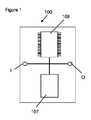
図1は、メモリ107とプロセッサ108と入力Iと出力Oとを備える装置100である。本実施の形態では、1つのプロセッサと1つのメモリしか示していないが、別の実施の形態では2以上のプロセッサおよび/または2以上のメモリ(例えば、同じまたは異なるプロセッサ/メモリタイプ)を用いてもよい。 FIG. 1 is a
本実施の形態では、装置100は、撮像デバイスまたはセンサ用の特定用途向け集積回路(ASIC)である。別の実施の形態では、装置100は、プロセッサ108がデバイスの汎用CPUであってメモリ107がデバイスに含まれる汎用メモリであるようなデバイス用のモジュールでも、そのデバイス自体でもよい。 In the present embodiment,
入力Iは、センサアレイなどのさらなる部品から装置100へのシグナリングの受け取りを可能にする。出力Oは、装置100内からさらなる部品へのシグナリングの送出を可能にする。本実施の形態では、入力Iおよび出力Oは、装置100とさらなる部品との接続を可能にする接続バスの一部である。 Input I enables the reception of signaling to
プロセッサ108は、コンピュータプログラムコードの形でメモリ107上に格納された命令に従い、入力Iを介して受け取った情報を実行/処理することに特化した汎用プロセッサである。このような動作により生成された、プロセッサ108からの出力シグナリングは、出力Oを介してさらなる部品へ送出される。 The
メモリ107(単一のメモリ部でなくてもよい)は、コンピュータプログラムコードを格納するコンピュータ読み取り可能な媒体(この例では固体メモリであるが、ハードドライブ、ROM、RAM、フラッシュなど別のタイプのメモリでもよい)である。このコンピュータプログラムコードは、プログラムコードをプロセッサ108で実行する際にプロセッサ108が実行可能な命令を格納している。メモリ107とプロセッサ108との内部接続とは、1以上の実施の形態例において、メモリ107上に格納されたコンピュータプログラムコードへプロセッサ108がアクセスできるようプロセッサ108とメモリ107とを動作可能につなげることと理解されよう。 Memory 107 (not necessarily a single memory portion) is a computer readable medium (in this example solid-state memory that stores computer program code, but another type of hard drive, ROM, RAM, flash, etc.) Memory). The computer program code stores instructions that can be executed by the
この例では、入力I、出力O、プロセッサ108、および、メモリ107は、各部品I、O、107、および、108が電気的にやり取りできるよう互いに全て内部電気接続されている。この例では、部品は、共にASICとして形成されるよう、言い換えれば、電子デバイスに組み込むことができる単一のチップ/回路として集積されるよう互いに全て近接した位置にある。別の例では、1以上または全ての部品が互いに離れた位置にあってもよい。 In this example, the input I, the output O, the
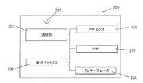
図2は、センサアレイを備えた電子デバイスなど、さらなる実施の形態例の装置200である。別の実施の形態例では、装置200は、電子デバイス用のモジュールを備えてもよいし、適切に構成されたメモリ207およびプロセッサ208をただ備えるだけでもよい。 FIG. 2 is a
図2の実施の形態例は、例えば、液晶ディスプレイ(LCD)、電子ペーパー、または、タッチスクリーンユーザーインターフェースなどの表示デバイス204を備える。図2の装置200は、データを受け取り、含み、および/または、そうでなければデータにアクセスするように構成される。例えば、この実施の形態例200は、1以上のタイプのネットワークを介してデータを受け取れるように、無線ネットワークに接続するためのアンテナ202と通信する、受信機、送信機、および/もしくは、送受信機などの通信部203、ならびに/または、ネットワークへの物理的な接続を可能にするポート(図示せず)を備える。この実施の形態例は、できれば、アンテナ202を介してデータを受信した後、または、ユーザインターフェース205でデータを生成した後でそのデータを格納するメモリ207を備える。プロセッサ208は、ユーザインターフェース205、メモリ207、または、通信部203からデータを受け取ってもよい。特定の実施の形態例では、表示デバイス204がユーザインターフェース205を内蔵していてもよい。データの出所にかかわらず、これらのデータを、表示デバイス204、および/または、装置に設けられた他の出力デバイスを介して装置200のユーザに出力してもよい。また、プロセッサ208が、後で使用するためにメモリ207へデータを格納してもよい。メモリ207は、機能(例えば、データの読み込み、書き込み、削除、編集、または、加工)を実行するようプロセッサ208に命令するために/プロセッサ208が機能実行できるようにするために用いられる、コンピュータプログラムコードおよび/またはアプリケーションを格納してもよい。 The example embodiment of FIG. 2 includes a
図3は、タブレット型パーソナルコンピュータ、ポータブル電子デバイス、ポータブルテレコミュニケーションデバイス、このようなデバイスのサーバもしくはモジュールなど、図1の装置100を備える電子デバイス300のさらなる実施の形態例である。装置100は、デバイス300のモジュールとして、または、デバイス300用のプロセッサ/メモリ、もしくは、このようなデバイス300のモジュール用プロセッサ/メモリとしても提供することができる。デバイス300は、データバス380で接続(例えば、電気的接続および/または無線接続)されたプロセッサ308と記憶媒体307とを備える。このデータバス380によって、コンピュータプログラムコードへプロセッサ308がアクセスできるようプロセッサ308と記憶媒体307とは動作可能につなげられる。デバイス/装置の部品(例えば、メモリ、プロセッサ)は、クラウドコンピューティング構造を介して接続されてもよい。例えば、記憶装置は、プロセッサがインターネットを介してアクセスするリモートサーバでもよい。デバイス300は、センサアレイを用いて刺激を検出してもよい。 FIG. 3 is a further example embodiment of an
図3の装置100は、装置100から出力を受け取ってこの出力をデータバス380を介してデバイス300へ伝送する入力/出力インターフェース370に接続(例えば、電気的接続および/または無線接続)される。インターフェース370は、装置100からユーザへ情報を提供するディスプレイ304(接触検知またはその他)にデータバス380を介して接続可能である。ディスプレイ304は、デバイス300の一部でもよいし、別個のものでもよい。また、デバイス300は、他のデバイス部品の動作を管理するためにそれらへシグナリングを提供しそれらからシグナリングを受け取ることによって装置100およびデバイス300を通常制御するよう構成されたプロセッサ308を備える。 The
記憶媒体307は、装置100の動作を実行、制御、または、有効にするコンピュータコードを格納する。記憶媒体307は、他のデバイス部品の設定を格納してもよい。プロセッサ308は、他のデバイス部品の動作を管理するために、記憶媒体307にアクセスしてそれらの部品の設定を検索してもよい。記憶媒体307は、揮発性ランダムアクセスメモリなどの一時的な記憶媒体でもよい。また、記憶媒体307は、ハードディスクドライブ、フラッシュメモリ、(クラウドストレージなどの)リモートサーバ、または、不揮発性ランダムアクセスメモリなどの恒久的な記憶媒体でもよい。記憶媒体307は、同じまたは異なるメモリタイプの様々な組み合わせから構成されてもよい。 The
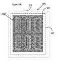
本発明は、センサアレイを用いて外部刺激または刺激を検知する装置に関する。アレイの複数のセンサによって、検知領域の範囲を規定してもよい。装置400は、それぞれが刺激を測定できる個別センサ401のセンサアレイを備え、組み合わせて、装置400の検知領域全体における刺激を表すデータを出力する。各センサ401の出力は、1以上の電気信号でもよい。センサアレイ402の総出力は、電子デバイスが受け取ってもよい。電子デバイスは、デジタルカメラ、赤外線カメラ、X線検出パネル、バイオセンシングプラットフォームでもよいし、電子デバイス300は、タブレット型パーソナルコンピュータ、ポータブル電子デバイス、ポータブルテレコミュニケーションデバイス、このようなデバイスのサーバもしくはモジュール、または、センサアレイ402もしくはここで説明する別の実施形態で構成される図1の装置100もしくは図2の装置200を備えるデバイスを備えてもよい。 The present invention relates to an apparatus for detecting an external stimulus or stimulus using a sensor array. The range of the detection area may be defined by a plurality of sensors in the array. The
センサアレイ402は、センサアレイ402に生成される適切な機能変換層を選択することにより、所望のタイプの刺激を検出するように構成されてもよい。装置が測定できる刺激は、温度、動き、光、放射物、生物学種、化学種などであるが、これらに限定されるものではない。したがって、所望の刺激に反応しやすいように機能変換層の材料または形を選択してもよい。別の実施の形態では、センサアレイ402は機能変換層を含まない。 The
図4は、本発明に係る装置400の実施の形態例である。装置400は、アレイ402状に配列された複数のセンサ401を備える。図4は、3×2状に配列された6つのセンサ401を示している。アレイ402の各センサ401は、電荷キャリアのソース を受けるドレイン電極403と、電荷キャリアの流れに対する電流シンクとなるソース電極404と、ドレイン電極403およびソース電極404間のチャネルの導電率を調整するように配列されたゲート電極405とを備える。アレイ402の各センサ401に共通する共通導電層または共通半導電層406は、アレイ402の複数のセンサ全体に延在するように配列される。共通導電層406は、各センサ401の少なくともソース電極404およびドレイン電極403と電気的に接するように構成される。この例では、共通導電層406は、ドレイン電極403およびソース電極404と電気的かつ物理的に接するように構成される。各センサ401のソース電極404は、アレイ402内のセンサ間におけるクロストークを防ぐために電荷キャリアが各センサ401のソース電極404を超えてドレイン電極403から流れないよう、各センサのドレイン電極403とゲート電極405とを実質的に取り囲む実質的に途切れのない境界を形成する。このように、ドレイン電極403に取り込まれた荷電キャリアは、通常、各センサの外側境界に位置するソース電極404に向かって流れる。当業者であれば、荷電キャリアは電子でも正孔でもよく、どちらかが特定デバイス実装における多数荷電キャリアになることは分かるであろう。ソース電極404の実質的に途切れのない配列は、ソース電極によって規定される、各センサ401の領域範囲を規定するセンサ境界を越えて荷電キャリアが漏れ出ないよう有利に働く。細長ソース電極は、チャネル長およびチャネル幅に沿った実質的に途切れのない境界を形成して、センサ境界を全体的に規定する。 FIG. 4 is an example embodiment of an
共通導電層406は、検知という目的に適していればどんな材料(薄膜材料など)でもよい。本発明では、共通導電層406はグラフェンである。グラフェン406は、デバイス製造段階においてダメージを受けやすいので、グラフェン406を装置400に施した後の処理ステップ数は最小限に抑えることが望ましい。 The common
各センサ401のソース電極404、ドレイン電極403、および、ゲート電極405は、デバイスチャネルとして機能するグラフェン層406(より一般的には、共通導電層または共通半導電層)と共に、電界効果トランジスタまたは電界効果トランスデューサ(FET)を形成する。電界効果トランジスタの配列において、ドレイン電極403およびソース電極404間の荷電キャリアの流れは、ゲート電極405にかかる電位の関数として表される。本発明では、導電層406が、ソース電極404およびドレイン電極403間で荷電キャリアが拡散できるチャネルの少なくとも一部を形成する。 The
グラフェン層406は、各センサ401のソース電極404およびドレイン電極403間に形成できる電界検知層全てにわたる領域となる。また、グラフェン層406は、機能変換層407と対応付けられるインターフェースにもなる。グラフェン406は局所的な電界変化に反応しやすいので、外部刺激の結果として局所的な電界変化を生じさせる材料との機能化により、効果的な機能変換層をグラフェンまたはその他の導電層と組み合わせて提供することができる。 The
図4の実施の形態において、ソース電極404は、アレイ内の2以上または全てのセンサ間で共有される共通ソース電極である。共通ソース電極404は、アレイ402の各センサのドレイン電極403それぞれにかかる荷電キャリアの流れに対して共通の電流シンクとなる。共通ソース電極404を用いて各センサのゲート電極405とドレイン電極403とをアレイ内の隣接するセンサから分離することにより、ソース電極404は、アレイ内のセンサ間におけるクロストークを防ぐ役割を果たす。この装置において、クロストークとは、概して不都合にセンサ間で伝達する信号、電磁場、または、荷電キャリアのことを指す。 In the embodiment of FIG. 4,
共通導電層を用いるかどうかに関わらず、センサ401の電極を適切な形状に設計することによって、特に、センサ間の外側境界または実質的に途切れのない境界として電流シンク電極を提供することによりクロストークを削減してもよい。 Regardless of whether or not a common conductive layer is used, the electrodes of the
性能および/または感度が有利になるように、各センサ401配列のチャネルの幅対長さパラメータを改良することが望ましい。幅対長さパラメータの改良を実現するために、ソース電極404は、各センサ401を実質的に取り囲んでいる境界431から内側へ延在するフィンガー部412を1以上備えることが望ましい。このように、ソース電極404は、境界部431と、そこから内側へ延在する少なくとも1つのフィンガー部412とを備えてもよい。また、少なくとも1つのセンサ401のドレイン電極403は、ソース電極404のフィンガー部412と互いに入り込むように設けられる、フィンガー部412の補足的なフィンガー部413を少なくとも1つ備えてもよい。図4は、ソース電極404が、ソース電極境界431から内側へ延在し、かつ、ドレイン電極のフィンガー部413と互いに入り込むように設けられるフィンガー部412をセンサ401ごとに4つ備える配列を示している。また、ソース電極404とドレイン電極403との間に位置するゲート電極405も補足フィンガー部を備えてよい。 It may be desirable to improve the channel width vs. length parameter of each
ソース電極403とドレイン電極404とを用いて、各センサからの検知値を決定してもよい。例えば、ソース電極とドレイン電極に電圧をかけて、その結果得られる電流値を測定してもよい。 The detection value from each sensor may be determined using the
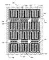
別の実施の形態では、さらなる電極を用いて、センサからの読み取りを行ってもよい。図5aおよび図5bに、第1センサ電極508と第2センサ電極509とをさらに備えた、図4と同様のさらなる装置500例を示す。センサアレイ502は、4つのセンサ502からなる2×2配列を備える。第1センサ電極508は、ソース電極504で実質的に取り囲まれてもよい。この例では、ソース電極504とゲート電極505との間に第1センサ電極508を配置する。第2センサ電極509はゲート電極505で実質的に取り囲まれてもよく、ゲート電極505とドレイン電極503との間に第2センサ電極509を配置する。 In another embodiment, additional electrodes may be used to read from the sensor. FIGS. 5 a and 5 b show a
アレイ502内の各センサ501のソース電極504は、ドレイン電極503を実質的に取り囲む実質的に途切れのない境界531を形成する。共通導電層506は、ソース電極、ドレイン電極、第1センサ電極、および、第2センサ電極と電気的に接するように構成される。ゲート電極は、図6において後で説明する誘電体層により共通導電層から分離されている。 The source electrode 504 of each
図6は、図5bの第1センサ電極と第2センサ電極とを備えたセンサアレイの断面図を示している。電極503、504、505、508、および、509は、基板510内に形成されてもよい。これらの電極は、CMOSまたはTFT技術を用いるなど適切な導体プロセス技術により形成されてもよい。そして、グラフェン層506を、例えば転写技術により、製造されたセンサアレイ502に生成してもよい。この後、グラフェン層506を機能化する以外では、さらなる処理ステップを装置500へ適用する必要はない。グラフェン層506は、機能変換層がない場合でも、特定の刺激に反応しやすくても構わない。 FIG. 6 shows a cross-sectional view of a sensor array comprising the first sensor electrode and the second sensor electrode of FIG. 5b.
誘電材料511は、ゲート電極505と共通導電層506との間に配置される。ゲート電極に電圧をかけることにより、チャネルの導電率を調整する電界を生じさせてもよい。当業者には自明のとおり、電界は、グラフェンチャネル内のキャリア密度(および型)を調整する役割を果たす。また、電界は、グラフェンのフェルミエネルギーも制御する。ソース電極504、ドレイン電極503、第1センサ電極508、および、第2センサ電極509は、共通導電層506と電気的に接する。また、これらは、本実施の形態において物理的にも接している。 The
1つの電極を別の電極で実質的に取り囲むということは、平面図で見た場合、つまり、基板510の平面において、電極が取り囲まれていることを意味していると分かるであろう。図6から明らかなように、電極は、基板510の平面の上方または下方では取り囲まれていない。このように、ソース電極405、505は、平面図において、実質的に途切れのない境界431、531を形成する。 It will be appreciated that substantially surrounding one electrode with another electrode means that the electrode is surrounded when viewed in plan view, ie, in the plane of the
電極は、ビアなどの電気的コネクタ615により読み出し回路614と接続される。これらの電気的コネクタ615は、電極503、504、505、508、および、509が形成される基板510を貫通してもよい。ビア615を一例として挙げたが、読み出し回路614に適した何らかの接続部を用いてもよい。ビア615は、ソース電極404、ゲート電極405、および、ドレイン電極403に対し、各センサ501の電極ごとに1以上設けられる。センサ電極508、509を1以上備える別の例では、センサ電極ごとにビアを1以上設けてもよい。別の実施の形態では、電極のうちいずれか1つが読み出し回路と1以上のビア615で接続していてもよい。 The electrode is connected to the
読み出し回路614は、センサアレイ502の1以上のセンサまたは各センサから少なくとも1つの電気的パラメータを検出するように構成される。読み出す電気的パラメータは、センサの抵抗値でも電流でも電圧でもよい。 The
図7は、各センサから順次電気的パラメータを測定して読み込むように構成された2×2のセンサアレイ502に対する読み出し回路700の例を示す。図4および図5に例示されているグラフェンFET(GFET)の構成を、グラフェン層507 が機能化されて検出するいかなる刺激に対しても反応しやすい可変抵抗716とみなしてもよい。読み出しにおいて個別センサ718、501の選択ができるよう、行列選択717をする手段が設けられる。読み出し回路700は、適切な行列選択717をすることにより、ソース電極とドレイン電極との間に電圧をかけて選択センサに荷電キャリアを流すように構成される。第1センサ電極508と第2センサ電極509との電圧差は、刺激に応じた検知値を示す。 FIG. 7 shows an example of a
別の方法として、アレイ502内の各センサの検知値を読み出すために、サンプルホールド回路構成800 を用いてもよい。サンプルホールド回路800は、多数のスイッチングトランジスタと少なくとも1つのストレージコンデンサとを備える。図8aおよび図8bは、ソース電極504、ゲート電極505、ドレイン電極503の他に2つのセンサ電極508、509を用いる単一センサと対応するように構成された読み出し回路の一部を示す。共通導電層506とのソース電極504、ドレイン電極503、第1センサ電極508、および、第2センサ電極509の接触抵抗は、回路図において抵抗818、819、820、および、821として図示される。これらの抵抗は、ビアの内部抵抗も表す。 Alternatively, the sample and hold circuit configuration 800 may be used to read the sensed value of each sensor in the
図8aに示す構成では、ソース電極とドレイン電極に電圧をかけることによってアレイの各センサ501を同時に動作させる。別の方法として、各センサのソース電極とドレイン電極に順に電圧をかけることによって、各センサ501を順次動作させてもよい。そして、アレイ502内のセンサの行列選択817をする手段を実装することによって、検知値を「格納」しているコンデンサ822およびコンデンサ823を順次読み取る。このように、検知値は、コンデンサ822とコンデンサ823に電荷を蓄えるために用いられる電圧として示される。そして、コンデンサの電荷は選択時に読み出される。 In the configuration shown in FIG. 8a, each
図8bは、抵抗値が既知の基準抵抗835と基準ストレージコンデンサ836とを含む別のサンプルホールド回路構成を示している。基準抵抗の抵抗値とvddの値とが分かれば、基準抵抗835における電圧がGFET716を流れる電流を示す。本実施の形態では、単一のコンデンサ822のみが、検知値の読み出しと対応付けられている。 FIG. 8b shows another sample and hold circuit configuration including a
図9a〜図9cは、図8aおよび図8bに示したFET構造の3つの変形例を示しており、それぞれ、センサ電極なし(2点構造)、1つのセンサ電極(3点構造)、2つのセンサ電極(4点構造)が用いられている。図9aでは、ソース電極とドレイン電極との間を流れる電流が検知値を示してもよい。図9bでは、第1センサとソース電極との間の電圧が検知値を示してもよい。図9cでは、第1センサ電極と第2センサ電極との間の電圧が検知値を示してもよい。 9a to 9c show three variations of the FET structure shown in FIGS. 8a and 8b, each without a sensor electrode (two-point structure), one sensor electrode (three-point structure), two Sensor electrodes (four-point structure) are used. In FIG. 9a, the current flowing between the source electrode and the drain electrode may indicate the detected value. In FIG. 9b, the voltage between the first sensor and the source electrode may indicate the detected value. In FIG. 9c, the voltage between the first sensor electrode and the second sensor electrode may indicate the detected value.
図10aおよび図10bは、図5aおよび図5bと同様の装置500およびセンサアレイ502の別の実施の形態を示している。したがって、同じ参照符号が用いられる。しかしながら、この例では、いずれの電極に対してもフィンガー部は設けられていない。図10aは、単一のセンサ素子501を示しており、図10bは、このようなセンサからなる、共通ソース電極504を有した3×2アレイ502を示している。センサ501ごとに、ソース電極504が、全体的に途切れのない境界となる。この例では、ソース電極504が、センサアレイ502内の各センサ501に対する共通ソース電極となる。このように、共通ソース電極504は、隣接するセンサへ荷電キャリアが流れ込むことを実質的に防ぐよう機能する。このように、細長ソース電極は、チャネル周辺のセンサの全体的に途切れのない境界を形成する。 FIGS. 10a and 10b show another embodiment of an
図11は、センサアレイの別の実施の形態を示している。この例では、各センサ1101が、ソース電極1104とドレイン電極1103とゲート電極1105とを備える。ソース電極1104は、各センサ1101のゲート電極1105とドレイン電極1103とを実質的に取り囲む実質的に途切れのない境界を形成するように配列される。センサアレイ1102内のセンサ1101ごとに、第1ソース電極ブレーク部1126が設けられる。センサアレイ1102内のセンサ1101ごとに、第2ソース電極ブレーク部1127が設けられる。ブレーク部は、ソース電極1104により設けられるもとは途切れのない境界における途切れからなる。ブレーク部は、ソース電極およびドレイン電極の細長い特性により定義される、チャネル幅よりもむしろチャネル長をまたいでいる。ゲート電極は、ソースとドレインとの間に配列され、本実施の形態では、第1ゲート電極ブレーク部1124が、センサアレイ1102内のセンサ1101ごとに設けられる。第2ゲート電極ブレーク部1125は、センサアレイ1102内のセンサ1101ごとに設けられる。この構成では、途切れのないグラフェン層1106がこれまでの実施の形態と同様に用いられる。ソース電極が途切れる領域において、隣接するセンサ間の間隔は、ソース電極が途切れていないつまり連続している領域よりも大きい。この例では、ブレーク部は各センサの片側に設けられる。ブレーク部が位置する側では、隣接するセンサ間に基板のスペースエリア1130が設けられる。ブレーク部がない側では、実質的に互いに接するように、特に、スペースエリア1130を含まないようにセンサが配列される。 FIG. 11 shows another embodiment of the sensor array. In this example, each
ブレーク部は、各センサを効果的に2つの部分に分け、各部分はグラフェンをベースにした電界効果トランジスタを備える。特に、ゲートブレーク部1124、1125、および、ソースブレーク部1126、1127により、基準センサ部1128と検知センサ部1129とが規定される。各基準センサ部1128はそれ自身の個別ソース電極を有し、また、検知センサ部1129の各ソース電極もそれ自身の個別ソース電極を有する。ソース電極は全て、接地電位に保持される。ソース電極とドレイン電極に電圧をかけると、検知センサ部と基準センサ部の両方に電流が流れる。ドレインへ流れる電流を測定し、基準センサ部1128のソース電極から流れ出る電流を測定する。このようにして、両部分の抵抗値を決定することができる。基準GFETは、機能化されておらず、温度補償用などの基準部品として機能する。 The break portion effectively divides each sensor into two parts, each part comprising a field effect transistor based on graphene. In particular, the
図12は、センサアレイ1200の別の実施の形態を示している。この例では、各センサ1201が、ソース電極1204とドレイン電極1203とゲート電極1205とを備える。ソース電極1204は、各センサ1201のゲート電極1205とドレイン電極1203とを実質的に取り囲む実質的に途切れのない境界を形成するように配列される。センサアレイ1202内のセンサ1201ごとに、第1ソース電極ブレーク部1226が設けられる。センサアレイ1202内のセンサ1201ごとに、第2ソース電極ブレーク部1227が設けられる。ブレーク部は、ソース電極1204により設けられるもとは途切れのない境界における途切れからなる。ゲート電極は、ソース電極とドレイン電極との間に配列され、本実施の形態では、第1ゲート電極ブレーク部1224が、センサアレイ1202内のセンサ1201ごとに設けられる。第2ゲート電極ブレーク部1225は、センサアレイ1202内のセンサ1201ごとに設けられる。この構成では、途切れのないグラフェン層1206がこれまでの実施の形態と同様に用いられる。ソース電極が途切れる領域において、隣接するセンサ間の間隔は、ソース電極が途切れていないつまり連続している領域よりも大きい。この例では、ブレーク部は各センサの片側に設けられる。ブレーク部が位置する側では、隣接するセンサ間に基板のスペースエリア1230が設けられる。ブレーク部がない側では、実質的に互いに接するように、特に、スペースエリア1230を含まないようにセンサが配列される。 FIG. 12 shows another embodiment of the
ブレーク部は、各センサを効果的に2つの部分に分け、各部分はグラフェンをベースにした電界効果トランジスタを備える。特に、ゲートブレーク部1224、1225、および、ソースブレーク部1226、1227により、基準センサ部1228と検知センサ部1229とが規定される。各基準センサ部1228はそれ自身の個別ソース電極を有する一方、検知センサ部1229のソース電極はアレイ内のセンササブセット間で共通ソースとなる。ソース電極は全て、接地電位に保持される。ソース電極とドレイン電極に電圧をかけると、検知センサ部と基準センサ部の両方に電流が流れる。 The break portion effectively divides each sensor into two parts, each part comprising a field effect transistor based on graphene. In particular, the
検知センサ部に流れる電流を測定し、基準センサ部1128のソース電極に流れる電流を測定する。このようにして、両部分の抵抗値を抽出することができる。基準GFETは、機能化されておらず、温度補償用などの基準部品として機能する。 The current flowing through the detection sensor unit is measured, and the current flowing through the source electrode of the
図13は、センサアレイ1300の別の実施の形態を示している。この例では、各センサ1301 が、細長ソース電極1304と、細長ドレイン電極1303と、細長ゲート電極1305とを備える。ソース電極1304は、各センサ1301のゲート電極1305とドレイン電極1303とを実質的に取り囲むように配列される。ソース電極は、第1ソース電極ブレーク部1331と第2ソース電極ブレーク部1332とを備える。ブレーク部は、ソース電極1304により設けられるもとは途切れのない境界における途切れからなる。ソース電極は、さらに、第1フィンガー部1333と第2フィンガー部1334とを備える。第1ソース電極ブレーク部1331は、第1フィンガー部1333に実質的に隣接して配列され、第2ソース電極ブレーク部1332は、第2フィンガー部1334に実質的に隣接して配列される。ゲート電極1305およびドレイン電極1303は、第1ブレーク部1331および第2ブレーク部1332内に延在する、つまり、第1ブレーク部1331および第2ブレーク部1332を実質的に埋めるように配列される。各センサ1301の第1ソース電極フィンガー部1333と第2ソース電極フィンガー部1334、および、各センサ1301の第1ソース電極ブレーク部1331と第2ソース電極ブレーク部1332の配列は、各センサのゲート電極1305とドレイン電極1303とが、各センサ1301を蛇行するパスを形成するように配列される。本発明の実施の形態において、アレイ内の各センサ1301のソース電極1304は、アレイ内の他の各センサのソース電極とは別個のものである。アレイ内の各センサ1301のソース電極1304は、アレイ内の各センサに対する共通ソース電極を形成しない。蛇行パス配列された第1センサと第2センサとを少なくとも備えるセンサアレイでは、第2センサが、第1ブレーク部または第2ブレーク部を備える第1センサの端に実質的に隣接して配列され、第2センサの第1ブレーク部または第2ブレーク部が、第1センサのブレーク部に実質的に隣接して配列される。当該技術分野における周知の配列と比較し、隣接するセンサのブレーク部が実質的に互いに隣接する配列は、隣接センサ間のクロストークを減らす役割を果たす。このように、各センサ素子の電極は、センサ境界において、隣接するセンサ素子の対応電極と対向していてもよい。したがって、隣接するセンサ素子と対向しているセンサ境界部分は、隣接するセンサ素子のセンサ境界の対向部分と実質的に同じ電位でもよい。 FIG. 13 shows another embodiment of the
図13のセンサ素子は、共通の行にあるセンサ素子(つまり、図13の上部センサ素子2つ)のレイアウトが実質的に同一であり、共通の行に隣接する行にあるセンサ素子(つまり、図13の下部センサ素子2つ)のレイアウトが共通の行にあるセンサ素子の実質的な鏡像である、行と列の格子状に配列される。 The sensor elements of FIG. 13 have substantially the same layout of sensor elements in a common row (ie, the two upper sensor elements of FIG. 13), and sensor elements in rows adjacent to the common row (ie, The layout of the two lower sensor elements of FIG. 13) is arranged in a grid of rows and columns, which is a substantial mirror image of the sensor elements in a common row.
さらに、各電極および各電極部分は細長部材である。アレイ1300内の第1センサを形成する電極は、アレイ内の隣接するセンサを形成する電極とつながっていない。このように、アレイ内の隣接センサ間には共通電極が設けられていない。ドレイン電極1303は、対応センサの第1辺1137 から対応センサの第2辺1338へ蛇行パスに沿って延在するように配列される。このように、ドレイン電極1303は、対応センサの第1辺1337から対応センサの第2辺1338へ、対応センサの第2辺1338に達する前まで長さに沿って向きを複数回変化させるように延在してもよい。第1ゲート電極部1305aの第1端は、第1ゲート電極部1305aが対応センサの第1辺1337から対応センサの第2辺1338へ延在するように、ドレイン電極1303の第1端に沿って延在する。第2ゲート電極部1305bの第1端は、第2ゲート電極部1305bが対応センサの第1辺1337から対応センサの第2辺1338へ延在するように、ドレイン電極1303の第2端に沿って延在する。第1ソース電極部1304aの第1端1337 は、第1ソース電極部1304aが対応センサの第1辺1337から対応センサの第2辺1338へ延在するように、第1ゲート電極部1305aの第2端1338 に沿って延在する。第2ソース電極部1304bの第1端は、第2ソース電極部1304bが対応センサの第1辺1337から対応センサの第2辺1338へ延在するように、第2ゲート電極部1305bの第2端に沿って延在する。 Furthermore, each electrode and each electrode portion is an elongated member. The electrodes forming the first sensor in the
このように、通常、ソース電極は、少なくとも、ドレイン電極の長手方向範囲で定義されるチャネル幅に沿って、蛇行ドレイン電極を囲んでセンサ境界となる複数の部分を備える。 As described above, the source electrode usually includes a plurality of portions that surround the meandering drain electrode and serve as sensor boundaries along at least the channel width defined by the longitudinal range of the drain electrode.
図14は、アレイ状に配列された複数のセンサを受け取るステップ1402と、共通導電層または共通半導電層を基板に生成するステップ1404とを示したフロー図である。用語「センサ」は、組立品のみが検知できるものになるのかもしれないが、ソース電極、ドレイン電極、ゲート電極、任意のセンサ電極、および、チャネルのレイアウトを定義するために用いられており、共通導電層または共通半導電層が生成され、任意の読み出し回路がセンサと対応付けられている。複数の電極を受け取るステップ1402は、CMOSまたはTFT技術を用いるなど任意の適切な導体プロセス技術により電極を形成する形成ステップを含んでもよい。共通導電層を生成するステップ1404は、グラフェンの場合などは別の基板上に形成された薄膜の転写や、化学蒸着、原子層堆積、物理蒸着といった蒸着法を用いた薄膜の堆積などでもよいし、ウェットコーティング、プリント、または、ラングミュアーブロジェット技術を用いた実質的な2次元プレートレットの溶剤から共通導電層を形成してもよい。この方法は、共通導電層または共通半導電層に機能変換層を生成するステップを含んでもよい。変換層は、ウェットコーティング(スピンコーティング、バーコーティング、スプレーコーティング)、プリント(インクジェット印刷、エアロゾルジェット堆積、グラビア印刷、フレキソ印刷)、または、ドライコーティング(熱蒸発、スパッタコーティング)などの堆積方法で生成してもよい。 FIG. 14 is a flow
グラフェンをセンサアレイに転写するステップは、例示として、以下のステップを含んでもよい。
1.銅箔などの金属触媒箔の両面にグラフェンをCVD成長させる。
2.PMMAなどの保護高分子層でグラフェン/Cu箔の片面をコーティングする。
3.グラフェン/Cu箔のもう一方の面からグラフェンを取り除く。
4.湿式化学エッチングで銅を取り除き、洗浄して洗い流す。
5.湿った状態で対象基板に保護層/グラフェンを生成して、乾かす。
6.アセトンなどの溶媒を用いて、または、熱処理によって保護層を取り除く。
7.対象基板上のグラフェンを熱アニール処理して、密着性をよくする。The step of transferring the graphene to the sensor array may include, for example, the following steps.
1. Graphene is grown on both sides of a metal catalyst foil such as copper foil by CVD.
2. One side of graphene / Cu foil is coated with a protective polymer layer such as PMMA.
3. Remove graphene from the other side of the graphene / Cu foil.
4). Remove copper by wet chemical etching, wash and wash away.
5. A protective layer / graphene is generated on the target substrate in a wet state and dried.
6). The protective layer is removed using a solvent such as acetone or by heat treatment.
7). The graphene on the target substrate is thermally annealed to improve the adhesion.
センサアレイ、電界効果トランジスタ、および、対応電極の形成は、フォトリソグラフィーなどの任意の適切な導体製造プロセスまたは半導体製造プロセスにより実現してもよい。さらに、共通導電層の生成を、任意の2次元物質処理プロセスにより実施してもよい。 The formation of the sensor array, field effect transistor, and corresponding electrode may be accomplished by any suitable conductor or semiconductor manufacturing process such as photolithography. Furthermore, the generation of the common conductive layer may be performed by any two-dimensional material treatment process.
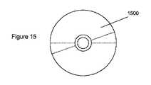
図15は、例に応じたプログラムを提供するコンピュータ読み取り可能媒体1500の概略図である。この例では、コンピュータ/プロセッサ読み取り可能媒体は、デジタル多用途ディスク(DVD)またはコンパクトディスク(CD)などのディスクである。別の例では、コンピュータ読み取り可能媒体は、発明機能を実行するようにプログラム化された任意のメディアでもよい。コンピュータプログラムコードを、ROM、RAM、フラッシュ、ハードディスク、ソリッドステートなど、同じタイプの複数のメモリ間、または、異なるタイプの複数のメモリ間で分配してもよい。コンピュータ/プロセッサ読み取り可能媒体1500は、図5、図6、図7、図8、図9、図9、図10、または、図11の装置を製造する命令を格納していてもよい。 FIG. 15 is a schematic diagram of a computer readable medium 1500 that provides a program according to an example. In this example, the computer / processor readable medium is a disk, such as a digital versatile disk (DVD) or a compact disk (CD). In another example, a computer readable medium may be any medium programmed to perform inventive functions. Computer program code may be distributed between multiple memories of the same type, such as ROM, RAM, flash, hard disk, solid state, etc., or between multiple memories of different types. Computer / processor readable medium 1500 may store instructions for manufacturing the apparatus of FIG. 5, FIG. 6, FIG. 7, FIG. 8, FIG. 9, FIG.
上述した例では、各センサの「境界」となるソース電極が示されているが、作成されるセンサ素子の型によっては、代わりにドレイン電極が「境界」となってソース電極を取り囲むことは分かるであろう。したがって、当業者であれば本願の教示を用いて分かるように、上記例のソース電極とドレイン電極は入れ替えが可能である。 In the above example, the source electrode that is the “boundary” of each sensor is shown. However, depending on the type of sensor element that is created, it can be seen that the drain electrode instead becomes the “boundary” and surrounds the source electrode. Will. Accordingly, as will be appreciated by those skilled in the art using the teachings of the present application, the source and drain electrodes in the above example can be interchanged.
上記例に示した装置は、カメラ、X線検出器、暗視ゴーグル、ポータブル電子機器、ノート型パソコン、携帯電話、スマートフォン、タブレット型コンピュータ、携帯情報端末、デジタルカメラ、スマートウォッチ、スマートメガネ、ペン型コンピュータ、据え置き型電子機器、デスクトップコンピュータ、モニタ、家電、スマートTV、サーバ、または、これら用のモジュール/回路に含まれていてもよい。いずれのデバイスも、刺激を処理するためにセンサアレイを必要とする。 The devices shown in the above examples are cameras, X-ray detectors, night vision goggles, portable electronic devices, notebook computers, mobile phones, smartphones, tablet computers, personal digital assistants, digital cameras, smart watches, smart glasses, pens Type computers, stationary electronic devices, desktop computers, monitors, home appliances, smart TVs, servers, or modules / circuits for these. Both devices require a sensor array to process the stimulus.
上述した装置/デバイス、および/または、特定の上述した装置/デバイスのその他の特徴も、有効になったときのみ、例えば、電源オンのときのみに所望の動作を実行するよう構成された装置で提供されてもよい。このような場合には、必ずしも、無効状態(例えば、電源オフ状態)でアクティブメモリに適切なソフトウェアをロードしておく必要はなく、有効状態(例えば、電源オン状態)でのみ適切なソフトウェアをロードすればよい。装置は、ハードウェア回路および/またはファームウェアを備えてもよい。装置は、メモリにロードされたソフトウェアを備えてもよい。このようなソフトウェア/コンピュータプログラムは、同じメモリ/プロセッサ/機能部、および/または、1以上のメモリ/プロセッサ/機能部に記録されてもよい。 An apparatus / device as described above, and / or other features of a particular above-described apparatus / device may also be implemented in an apparatus configured to perform a desired operation only when enabled, for example, only at power-on. May be provided. In such a case, it is not always necessary to load the appropriate software into the active memory in the invalid state (for example, the power-off state), and the appropriate software is loaded only in the valid state (for example, the power-on state). do it. The device may comprise hardware circuitry and / or firmware. The device may comprise software loaded into the memory. Such software / computer programs may be recorded in the same memory / processor / function unit and / or in one or more memory / processor / function units.
いくつかの例では、特定の上述した装置/デバイスが、所望の動作を実行するための適切なソフトウェアで予めプログラム化されていてもよく、この適切なソフトウェアは、例えば、ユーザが「キー」をダウンロードしてソフトウェアおよび対応機能をアンロック/有効化することによって使用可能になる。このような例には、デバイスにさらなる機能が必要になった場合にデータをダウンロードする必要が減るなどの利点があり、これは、ユーザが有効化しないかもしれない機能を予めプログラム化したソフトウェアを格納しておく容量がデバイスに十分あるとされる例において有益である。 In some examples, certain above-described devices / devices may be pre-programmed with appropriate software to perform a desired operation, such as when a user presses a “key”. It can be used by downloading and unlocking / enabling the software and corresponding functions. Such an example has the advantage of reducing the need to download data when the device needs more functionality, which means that software that has been pre-programmed with functionality that the user may not enable. This is useful in examples where the device has enough storage capacity.
上述した装置/回路は、上述した機能の他に別の機能を有してもよく、これら別の機能は同一の装置/回路で実行されてもよい。開示された1以上の態様には、適切なキャリア(例えば、メモリ、信号)に記録された(符号化して調達/運搬されてもよい)コンピュータプログラムおよび対応コンピュータプログラムの電子配布が含まれてもよい。 The devices / circuits described above may have other functions in addition to the functions described above, and these other functions may be performed by the same device / circuit. One or more disclosed aspects may include electronic distribution of computer programs and corresponding computer programs recorded on suitable carriers (eg, memory, signals) (which may be sourced / carried encoded) Good.
ここで述べたいずれの「コンピュータ」も、1以上の個別プロセッサ/処理要素の一群を備え、これらは、同じ回路基板上または回路基板の同じ領域/位置もしくは同じデバイス上にあってもなくてもよい。いくつかの例では、1以上の上述したプロセッサを複数のデバイスで分配してもよい。同じまたは異なるプロセッサ/処理要素が、ここで述べた1以上の機能を実行してもよい。 Any “computer” described herein comprises a group of one or more individual processors / processing elements, which may or may not be on the same circuit board or on the same area / location of the circuit board or on the same device. Good. In some examples, one or more of the above-described processors may be distributed across multiple devices. The same or different processors / processing elements may perform one or more of the functions described herein.
用語「シグナリング」は、一連の送受信電気信号/光信号として伝送される1以上の信号のことを指してもよい。一連の信号は、前記シグナリングを形成するために、1、2、3、4、もしくは、それ以上の個別信号成分または異なる信号を含んでもよい。これら個別信号のいくつかまたは全てを、無線または有線で、同時、順次、および/または、一時的に重複するように送受信してもよい。 The term “signaling” may refer to one or more signals transmitted as a series of transmitted / received electrical / optical signals. The series of signals may include 1, 2, 3, 4, or more individual signal components or different signals to form the signaling. Some or all of these individual signals may be transmitted and received in a wireless or wired manner, simultaneously, sequentially, and / or temporarily overlapping.
上述したコンピュータおよび/またはプロセッサおよびメモリ(例えば、ROM、CD−ROMなど)の内容に関して、これらは、コンピュータプロセッサ、特定用途向け集積回路(ASIC)、フィールド・プログラマブル・ゲート・アレイ(FPGA)、および/または、発明機能を実行するようにプログラム化されたその他のハードウェア部品を備えていてもよい。 With respect to the contents of the computers and / or processors and memories (eg, ROM, CD-ROM, etc.) described above, these include computer processors, application specific integrated circuits (ASICs), field programmable gate arrays (FPGAs), and And / or other hardware components programmed to perform inventive functions.
出願人は、ここに記載した特徴はそれぞれ別個でも組み合わせても、このような特徴またはそれらの組み合わせが、ここに開示した課題を解決するかどうかにかかわらず、請求項の範囲を限定することなく、当業者の一般知識と照らし合わせて、全体として本明細書に基づいて実行できる範囲でここに開示する。出願人は、開示した態様/実施例がこのような個々の特徴またはそれらの組み合わせからなることを示している。前述の記載を考えると、様々な変形例が開示の範囲内でなされてもよいことは当業者にとって自明であろう。 Applicants may determine whether the features described herein are separate or combined, regardless of whether such features or combinations thereof solve the problems disclosed herein without limiting the scope of the claims. In the light of general knowledge of those skilled in the art, and disclosed herein to the extent that it can be implemented based on the present specification as a whole. Applicants have shown that the disclosed aspects / examples consist of such individual features or combinations thereof. In view of the foregoing description it will be evident to a person skilled in the art that various modifications may be made within the scope of the disclosure.
例に適用したような基本的新規特徴を示して説明し指摘しているが、開示の範囲を逸脱することなく、説明したデバイスおよび方法の形状および詳細における様々な省略、代替、および、変更がなされてもよいことは当業者であれば理解されよう。例えば、同じ結果を得るために実質的に同じ方法で実質的に同じ機能を実行する要素および/または方法ステップの全ての組み合わせは、本開示の範囲内であることは明らかである。また、開示された形状または例に関連して示されたおよび/または説明された構造および/または要素および/または方法ステップは、設計上の選択という通常の事柄として、開示または説明または示唆された別の形状または例に包含されてもよい。さらに、ミーンズ・プラス・ファンクション節は、記載した機能、および、構造的な等価物だけでなく同等の構造物も実行するように、ここで説明した構造をカバーすることを目的としている。このように、くぎとねじは、くぎは円筒状の表面を用いて木材同士を固定するという点で構造的な等価物ではないかもしれないが、ねじはらせん状の表面を用いており、木材を留めるという状況においては、くぎとねじは同等の構造物である。 While the basic novel features as applied to the examples have been shown and described and pointed out, various omissions, substitutions and changes in the form and details of the described devices and methods may be made without departing from the scope of the disclosure. Those skilled in the art will understand that this may be done. For example, it is apparent that all combinations of elements and / or method steps that perform substantially the same function in substantially the same way to achieve the same result are within the scope of the disclosure. Also, the structures and / or elements and / or method steps shown and / or described in connection with the disclosed shapes or examples are disclosed or described or suggested as a matter of design choice. Other shapes or examples may be included. Further, the Means Plus Function section is intended to cover the structures described herein to perform the described functions and equivalent structures as well as structural equivalents. Thus, nails and screws may not be structural equivalents in that nails use a cylindrical surface to secure wood to each other, but screws use a spiral surface and wood In the situation of fastening, the nail and screw are equivalent structures.
Claims (16)
Translated fromJapanese各センサがソース電極とドレイン電極とチャネルとを有し、前記ソース電極および前記ドレイン電極のいずれか一方が前記チャネルに注入する荷電キャリアの流れを受け取り、他方が前記チャネルからの前記荷電キャリアの流れに対する電流シンクとなり、前記ソース電極と前記ドレイン電極とは細長く、前記チャネルのチャネル幅は前記ソース電極および/または前記ドレイン電極の長手方向範囲で定義され、前記チャネルのチャネル長は前記ソース電極と前記ドレイン電極との間隔によって定義される複数のセンサと、
前記アレイ状の複数のセンサ全体に延在するように配列され、各センサの少なくとも前記ソース電極および前記ドレイン電極と電気的に接している共通導電層または共通半導電層とを備え、
各センサの前記ソース電極および前記ドレイン電極のいずれか一方が、実質的に途切れのないセンサ境界であって、前記アレイ内のセンサ間におけるクロストークを防ぐために前記電荷キャリアの流れが前記センサ境界を超えないよう各センサの他方の電極を実質的に取り囲むセンサ境界を少なくとも前記チャネル幅に沿って形成する
装置。A plurality of sensors arranged in an array,
Each sensor has a source electrode, a drain electrode, and a channel, and one of the source electrode and the drain electrode receives a flow of charge carriers injected into the channel, and the other receives a flow of the charge carriers from the channel. The source electrode and the drain electrode are elongated, the channel width of the channel is defined by the longitudinal range of the source electrode and / or the drain electrode, and the channel length of the channel is the source electrode and the A plurality of sensors defined by the distance to the drain electrode;
A common conductive layer or a common semiconductive layer arranged so as to extend over the plurality of sensors in the array and in electrical contact with at least the source electrode and the drain electrode of each sensor;
Either the source electrode or the drain electrode of each sensor is a substantially uninterrupted sensor boundary, and the flow of charge carriers crosses the sensor boundary to prevent crosstalk between the sensors in the array. Forming a sensor boundary substantially at least along the channel width that substantially surrounds the other electrode of each sensor so as not to exceed.
請求項1に記載の装置。The device according to claim 1, wherein the conductive layer or the semiconductive layer is associated with a function conversion layer.
請求項1または2に記載の装置。Each sensor includes a gate electrode arranged to adjust the conductivity of the channel between the drain electrode and the source electrode, and a dielectric material is formed between the gate electrode and the common conductive layer or the common semiconductive layer. The device according to claim 1, which is arranged between.
請求項1〜3のいずれかに記載の装置。The apparatus according to claim 1, wherein the electrodes forming the boundary comprise a common electrode for all or a subset of sensors in the array.
請求項4に記載の装置。The apparatus of claim 4, wherein the electrodes forming the boundary are arranged in a grid that defines the boundaries of each sensor in the array.
請求項1〜5のいずれかに記載の装置。The apparatus according to claim 1, wherein the source electrode, the gate electrode, and the drain electrode of each sensor in the array are configured as part of a field effect transducer (FET).
前記第一面に対向する前記基板の第二面に配置されて、貫通ビアを介して前記複数のセンサと相互接続されるか、
前記複数のセンサの下方にある前記基板に埋め込まれて、前記センサ電極と接続されるか、または、
別個の基板上に配置されて、電気接続により前記センサアレイと接続される
請求項1〜6のいずれかに記載の装置。The plurality of sensors are formed on a substrate, the common conductive layer is located on the first surface of the substrate, and a readout circuit that reads outputs of the plurality of sensors in the array includes:
Disposed on the second surface of the substrate opposite the first surface and interconnected with the plurality of sensors via through vias;
Embedded in the substrate below the plurality of sensors and connected to the sensor electrodes, or
The apparatus according to claim 1, wherein the apparatus is disposed on a separate substrate and connected to the sensor array by an electrical connection.
請求項1〜7のいずれかに記載の装置。The apparatus according to claim 1, wherein the common conductive layer or the common semiconductive layer is uninterrupted and is not substantially patterned across the plurality of sensors.
2次元材料の単一層、
2次元材料の二層、
2次元材料の複数層
から選択された2次元材料を含む
請求項1〜8のいずれかに記載の装置。The common conductive layer or the common semiconductive layer is:
A single layer of two-dimensional material,
Two layers of two-dimensional material,
The apparatus according to any one of claims 1 to 8, comprising a two-dimensional material selected from a plurality of layers of two-dimensional material.
請求項1〜9のいずれかに記載の装置。The device according to claim 1, wherein the common conductive layer or the common semiconductive layer is graphene.
リガンドでカプセル化されたコロイド量子ドットの層、
導体または半導体ナノ結晶の層、
圧電材料、
焦電膜、
生化学種
から選択される
請求項1〜10のいずれかに記載の装置。The function conversion layer is
A layer of colloidal quantum dots encapsulated with a ligand,
Layers of conductor or semiconductor nanocrystals,
Piezoelectric material,
Pyroelectric film,
The device according to claim 1, which is selected from biochemical species.
前記アレイの1以上のセンサに対して、前記ソース電極の1以上のフィンガー部と互いに入り込むように設けられる1以上のフィンガー部を形成するように前記1以上のセンサの前記ドレイン電極および前記ゲート電極を配列する
請求項1〜11のいずれかに記載の装置。The source electrode includes a boundary portion and one or more finger portions extending inward from the boundary portion,
The drain electrode and the gate electrode of the one or more sensors so as to form one or more finger portions that are provided so as to enter the one or more finger portions of the source electrode with respect to the one or more sensors of the array. The apparatus according to claim 1.
前記読み出し回路は、センサごとに前記ソース電極、前記ドレイン電極、前記第1センサ電極、および、前記第2センサ電極からの電気的パラメータの測定結果を用いて各センサの検知値を検出する
請求項1〜12のいずれかに記載の装置。A first sensor electrode extending between the source electrode and the gate electrode; a second sensor electrode extending between the gate electrode and the drain electrode;
The readout circuit detects a detection value of each sensor using a measurement result of an electrical parameter from the source electrode, the drain electrode, the first sensor electrode, and the second sensor electrode for each sensor. The apparatus in any one of 1-12.
各センサの前記ソース電極および前記ドレイン電極のいずれか一方が、実質的に途切れのないセンサ境界であって、前記アレイ内のセンサ間におけるクロストークを防ぐために前記電荷キャリアの流れが前記センサ境界を超えないよう各センサの他方の電極を実質的に取り囲むセンサ境界を少なくとも前記チャネル幅に沿って形成する、前記アレイ状の複数のセンサ全体に延在するように配列され、各センサの少なくとも前記ソース電極および前記ドレイン電極と電気的に接している共通導電層または共通半導電層を生成するステップとを含む
装置形成方法。A plurality of sensors arranged in an array, each sensor having a source electrode, a drain electrode, and a channel, wherein one of the source electrode and the drain electrode is configured to flow a charge carrier injected into the channel. The other is a current sink for the flow of the charge carriers from the channel, the source and drain electrodes are elongated, and the channel width of the channel is defined by the longitudinal extent of the source and / or drain electrode Receiving a plurality of sensors, wherein a channel length of the channel is defined by a distance between the source electrode and the drain electrode;
Either the source electrode or the drain electrode of each sensor is a substantially uninterrupted sensor boundary, and the flow of charge carriers crosses the sensor boundary to prevent crosstalk between the sensors in the array. At least the source of each sensor arranged across the plurality of sensors in the array, forming a sensor boundary substantially surrounding the other electrode of each sensor so as not to exceed, at least along the channel width. Forming a common conductive layer or a common semiconductive layer in electrical contact with the electrode and the drain electrode.
機能変換層を前記共通導電層に生成するステップを含む
請求項14に記載の装置形成方法。After generating the conductive layer or the semiconductive layer,
The device forming method according to claim 14, further comprising: generating a function conversion layer in the common conductive layer.
請求項14に記載の装置形成方法。15. The method of forming an apparatus according to claim 14, including the step of changing the width versus length parameter of the channel to improve the sensitivity of the sensor.
Applications Claiming Priority (3)
| Application Number | Priority Date | Filing Date | Title |
|---|---|---|---|
| EP15159721.8AEP3070741B1 (en) | 2015-03-18 | 2015-03-18 | An apparatus comprising a sensor arrangemenet and associated fabrication method |
| EP15159721.8 | 2015-03-18 | ||
| PCT/FI2016/050128WO2016146884A1 (en) | 2015-03-18 | 2016-03-02 | An apparatus comprising a sensor arrangement and associated fabrication methods |
Publications (2)
| Publication Number | Publication Date |
|---|---|
| JP2018509768Atrue JP2018509768A (en) | 2018-04-05 |
| JP6646060B2 JP6646060B2 (en) | 2020-02-14 |
Family
ID=52736865
Family Applications (1)
| Application Number | Title | Priority Date | Filing Date |
|---|---|---|---|
| JP2017549073AActiveJP6646060B2 (en) | 2015-03-18 | 2016-03-02 | Device with sensor array and method of manufacturing the same |
Country Status (5)
| Country | Link |
|---|---|
| US (1) | US10566425B2 (en) |
| EP (1) | EP3070741B1 (en) |
| JP (1) | JP6646060B2 (en) |
| CA (1) | CA2978178C (en) |
| WO (1) | WO2016146884A1 (en) |
Families Citing this family (6)
| Publication number | Priority date | Publication date | Assignee | Title |
|---|---|---|---|---|
| EP3206212B1 (en) | 2016-02-15 | 2022-03-02 | Nokia Technologies Oy | An apparatus and method of forming an apparatus comprising two dimensional material |
| CN105679678A (en)* | 2016-03-18 | 2016-06-15 | 武汉华星光电技术有限公司 | Preparation method for graphene thin film transistor |
| EP3261131B1 (en) | 2016-06-21 | 2022-06-22 | Nokia Technologies Oy | An apparatus for sensing electromagnetic radiation |
| CN107204375B (en)* | 2017-05-19 | 2019-11-26 | 深圳市华星光电技术有限公司 | Thin film transistor and its manufacturing method |
| GB2570487A (en) | 2018-01-26 | 2019-07-31 | Emberion Oy | Voltage-mode photosensitive device |
| WO2023213500A1 (en)* | 2022-05-05 | 2023-11-09 | Asml Netherlands B.V. | Radiation tolerant detector architecture for charged particle detection |
Citations (18)
| Publication number | Priority date | Publication date | Assignee | Title |
|---|---|---|---|---|
| JPH08148688A (en)* | 1994-11-22 | 1996-06-07 | Fuji Xerox Co Ltd | Thin-film semiconductor device and manufacture thereof |
| JPH1093062A (en)* | 1996-09-11 | 1998-04-10 | Toshiba Corp | Photodetector |
| JP2003332552A (en)* | 2002-05-15 | 2003-11-21 | Konica Minolta Holdings Inc | Reflectivity detecting element, sheet-like image input device, and sheet-like image input method |
| US20050127357A1 (en)* | 2003-12-12 | 2005-06-16 | Palo Alto Research Center, Inc. | Thin-film transistor array with ring geometry |
| JP2010129881A (en)* | 2008-11-28 | 2010-06-10 | Sharp Corp | Thin-film transistor and active matrix substrate |
| US20110156114A1 (en)* | 2009-12-29 | 2011-06-30 | Samsung Electronics Co., Ltd. | Image sensor using light-sensitive transparent oxide semiconductor material |
| US20110315949A1 (en)* | 2010-06-24 | 2011-12-29 | Nokia Corporation | Apparatus and method for sensing photons |
| JP2012053050A (en)* | 2011-10-05 | 2012-03-15 | Univ Of Tokyo | Non-single-crystal transistor integrated circuit |
| WO2012145247A1 (en)* | 2011-04-14 | 2012-10-26 | Regents Of The University Of Minnesota | An ultra-compact, passive, varactor-based wireless sensor using quantum capacitance effect in graphene |
| JP2012212877A (en)* | 2011-03-23 | 2012-11-01 | National Institute Of Advanced Industrial & Technology | Electronic device and manufacturing method of the same |
| JP2012528476A (en)* | 2009-05-25 | 2012-11-12 | ビーエーエスエフ ソシエタス・ヨーロピア | Crosslinkable dielectric, and methods for making and using the same |
| JP2013153177A (en)* | 2007-02-02 | 2013-08-08 | Semiconductor Energy Lab Co Ltd | Light-emitting device |
| WO2014162055A1 (en)* | 2013-04-05 | 2014-10-09 | Nokia Corporation | Transparent photodetector for mobile devices |
| US20140332757A1 (en)* | 2013-05-10 | 2014-11-13 | International Business Machines Corporation | Graphene photodetector |
| JP2015500482A (en)* | 2011-12-05 | 2015-01-05 | ザ トラスティーズ オブ ザ ユニバーシティ オブ ペンシルバニア | Graphene-Biomolecular Bioelectronic Device |
| WO2015012186A1 (en)* | 2013-07-25 | 2015-01-29 | 東レ株式会社 | Carbon nanotube composite, semiconductor device, and sensor using same |
| WO2015015700A1 (en)* | 2013-08-02 | 2015-02-05 | シャープ株式会社 | Semiconductor device for radiation detection |
| JP2015031666A (en)* | 2013-08-06 | 2015-02-16 | 日本電信電話株式会社 | Sensor element |
Family Cites Families (5)
| Publication number | Priority date | Publication date | Assignee | Title |
|---|---|---|---|---|
| TWI282956B (en)* | 2000-05-09 | 2007-06-21 | Sharp Kk | Data signal line drive circuit, and image display device incorporating the same |
| JP4109858B2 (en)* | 2001-11-13 | 2008-07-02 | 株式会社東芝 | Solid-state imaging device |
| US9817137B2 (en)* | 2014-01-15 | 2017-11-14 | Sharp Kabushiki Kaisha | Energy ray detector |
| KR102237826B1 (en)* | 2014-07-18 | 2021-04-08 | 삼성전자주식회사 | Graphene device, methods of manufacturing and operating the same, and electronic apparatus including graphene device |
| US9461088B2 (en)* | 2014-12-01 | 2016-10-04 | Omnivision Technologies, Inc. | Image sensor pixel with multiple storage nodes |
- 2015
- 2015-03-18EPEP15159721.8Apatent/EP3070741B1/enactiveActive
- 2016
- 2016-03-02JPJP2017549073Apatent/JP6646060B2/enactiveActive
- 2016-03-02CACA2978178Apatent/CA2978178C/enactiveActive
- 2016-03-02USUS15/558,237patent/US10566425B2/enactiveActive
- 2016-03-02WOPCT/FI2016/050128patent/WO2016146884A1/ennot_activeCeased
Patent Citations (18)
| Publication number | Priority date | Publication date | Assignee | Title |
|---|---|---|---|---|
| JPH08148688A (en)* | 1994-11-22 | 1996-06-07 | Fuji Xerox Co Ltd | Thin-film semiconductor device and manufacture thereof |
| JPH1093062A (en)* | 1996-09-11 | 1998-04-10 | Toshiba Corp | Photodetector |
| JP2003332552A (en)* | 2002-05-15 | 2003-11-21 | Konica Minolta Holdings Inc | Reflectivity detecting element, sheet-like image input device, and sheet-like image input method |
| US20050127357A1 (en)* | 2003-12-12 | 2005-06-16 | Palo Alto Research Center, Inc. | Thin-film transistor array with ring geometry |
| JP2013153177A (en)* | 2007-02-02 | 2013-08-08 | Semiconductor Energy Lab Co Ltd | Light-emitting device |
| JP2010129881A (en)* | 2008-11-28 | 2010-06-10 | Sharp Corp | Thin-film transistor and active matrix substrate |
| JP2012528476A (en)* | 2009-05-25 | 2012-11-12 | ビーエーエスエフ ソシエタス・ヨーロピア | Crosslinkable dielectric, and methods for making and using the same |
| US20110156114A1 (en)* | 2009-12-29 | 2011-06-30 | Samsung Electronics Co., Ltd. | Image sensor using light-sensitive transparent oxide semiconductor material |
| US20110315949A1 (en)* | 2010-06-24 | 2011-12-29 | Nokia Corporation | Apparatus and method for sensing photons |
| JP2012212877A (en)* | 2011-03-23 | 2012-11-01 | National Institute Of Advanced Industrial & Technology | Electronic device and manufacturing method of the same |
| WO2012145247A1 (en)* | 2011-04-14 | 2012-10-26 | Regents Of The University Of Minnesota | An ultra-compact, passive, varactor-based wireless sensor using quantum capacitance effect in graphene |
| JP2012053050A (en)* | 2011-10-05 | 2012-03-15 | Univ Of Tokyo | Non-single-crystal transistor integrated circuit |
| JP2015500482A (en)* | 2011-12-05 | 2015-01-05 | ザ トラスティーズ オブ ザ ユニバーシティ オブ ペンシルバニア | Graphene-Biomolecular Bioelectronic Device |
| WO2014162055A1 (en)* | 2013-04-05 | 2014-10-09 | Nokia Corporation | Transparent photodetector for mobile devices |
| US20140332757A1 (en)* | 2013-05-10 | 2014-11-13 | International Business Machines Corporation | Graphene photodetector |
| WO2015012186A1 (en)* | 2013-07-25 | 2015-01-29 | 東レ株式会社 | Carbon nanotube composite, semiconductor device, and sensor using same |
| WO2015015700A1 (en)* | 2013-08-02 | 2015-02-05 | シャープ株式会社 | Semiconductor device for radiation detection |
| JP2015031666A (en)* | 2013-08-06 | 2015-02-16 | 日本電信電話株式会社 | Sensor element |
Also Published As
| Publication number | Publication date |
|---|---|
| EP3070741A1 (en) | 2016-09-21 |
| US20180047814A1 (en) | 2018-02-15 |
| US10566425B2 (en) | 2020-02-18 |
| WO2016146884A1 (en) | 2016-09-22 |
| EP3070741B1 (en) | 2020-07-29 |
| CA2978178A1 (en) | 2016-09-22 |
| JP6646060B2 (en) | 2020-02-14 |
| CA2978178C (en) | 2022-08-23 |
Similar Documents
| Publication | Publication Date | Title |
|---|---|---|
| JP6646060B2 (en) | Device with sensor array and method of manufacturing the same | |
| JP6267805B2 (en) | Apparatus and related methods | |
| Liu et al. | Polyelectrolyte dielectrics for flexible low‐voltage organic thin‐film transistors in highly sensitive pressure sensing | |
| EP3012847B1 (en) | A multilayer graphene composite | |
| CN107278330B (en) | Field effect device, related device and method | |
| EP3214656B1 (en) | A quantum dot photodetector apparatus and associated methods | |
| US10312398B2 (en) | Sensing apparatus | |
| Lebedev et al. | Investigation of sensing capabilities of organic bi-layer thermistor in wearable e-textile and wireless sensing devices | |
| CN108700471A (en) | thermal pattern sensor | |
| EP3131121B1 (en) | Method for making a graphene-based field-effect apparatus | |
| Kyaw et al. | A polymer transistor array with a pressure-sensitive elastomer for electronic skin | |
| US20070051940A1 (en) | Device and method for determining the physical condition of an animal | |
| EP3104416A1 (en) | An apparatus for field effect transistor based devices and associated methods | |
| JP7270920B2 (en) | Chemical/Physical Phenomenon Detector | |
| EP3671871B1 (en) | Method for manufacturing a device comprising a material acquiring electrical properties after being subjected to electrical polarisation | |
| Karimi-Alavijeh et al. | An analytical solution for contact resistance of staggered organic field-effect transistors | |
| KR101967113B1 (en) | 3 Dimensional Transistor Sensors and Fabrication Method thereof | |
| Dahiya et al. | Integrated Tactile Sensing on Silicon |
Legal Events
| Date | Code | Title | Description |
|---|---|---|---|
| A521 | Request for written amendment filed | Free format text:JAPANESE INTERMEDIATE CODE: A523 Effective date:20171030 | |
| A621 | Written request for application examination | Free format text:JAPANESE INTERMEDIATE CODE: A621 Effective date:20171030 | |
| A977 | Report on retrieval | Free format text:JAPANESE INTERMEDIATE CODE: A971007 Effective date:20180712 | |
| A131 | Notification of reasons for refusal | Free format text:JAPANESE INTERMEDIATE CODE: A131 Effective date:20180828 | |
| A521 | Request for written amendment filed | Free format text:JAPANESE INTERMEDIATE CODE: A523 Effective date:20181113 | |
| A131 | Notification of reasons for refusal | Free format text:JAPANESE INTERMEDIATE CODE: A131 Effective date:20190416 | |
| A521 | Request for written amendment filed | Free format text:JAPANESE INTERMEDIATE CODE: A523 Effective date:20190704 | |
| TRDD | Decision of grant or rejection written | ||
| A01 | Written decision to grant a patent or to grant a registration (utility model) | Free format text:JAPANESE INTERMEDIATE CODE: A01 Effective date:20191217 | |
| A61 | First payment of annual fees (during grant procedure) | Free format text:JAPANESE INTERMEDIATE CODE: A61 Effective date:20200109 | |
| R150 | Certificate of patent or registration of utility model | Ref document number:6646060 Country of ref document:JP Free format text:JAPANESE INTERMEDIATE CODE: R150 | |
| R250 | Receipt of annual fees | Free format text:JAPANESE INTERMEDIATE CODE: R250 | |
| R250 | Receipt of annual fees | Free format text:JAPANESE INTERMEDIATE CODE: R250 | |
| R250 | Receipt of annual fees | Free format text:JAPANESE INTERMEDIATE CODE: R250 |