JP2018200951A - Semiconductor device, memory device, and manufacturing method of semiconductor device - Google Patents
Semiconductor device, memory device, and manufacturing method of semiconductor deviceDownload PDFInfo
- Publication number
- JP2018200951A JP2018200951AJP2017104813AJP2017104813AJP2018200951AJP 2018200951 AJP2018200951 AJP 2018200951AJP 2017104813 AJP2017104813 AJP 2017104813AJP 2017104813 AJP2017104813 AJP 2017104813AJP 2018200951 AJP2018200951 AJP 2018200951A
- Authority
- JP
- Japan
- Prior art keywords
- electrode
- electrodes
- semiconductor chip
- dendrite structure
- semiconductor device
- Prior art date
- Legal status (The legal status is an assumption and is not a legal conclusion. Google has not performed a legal analysis and makes no representation as to the accuracy of the status listed.)
- Granted
Links
Images


Landscapes
- Wire Bonding (AREA)
- Semiconductor Memories (AREA)
Abstract
Translated fromJapaneseDescription
Translated fromJapanese本発明は、半導体装置、記憶装置、及び半導体装置の製造方法に関する。 The present invention relates to a semiconductor device, a memory device, and a method for manufacturing a semiconductor device.
第1部品の第1電極と第2部品の第2電極とを導通させる様々な方法が知られている。例えば、第1部品の第1電極と第2部品の第2電極の間に導電性微粒子を含有する絶縁性接着剤を配置する。そして、第1電極と第2電極の間に電圧を印加して導電性微粒子を電極近傍に集めた後に第1電極と第2電極で導電性微粒子を挟みつけることで、第1電極と第2電極を導通させる方法が知られている(例えば、特許文献1)。例えば、第1部品の第1電極と第2部品の第2電極の間に導電性フィラーを含有する樹脂を配置する。そして、第1電極と第2電極の間に電圧を印加して導電性フィラーを電極近傍に集めた後に導電性フィラーを溶融させて導通部を形成することで、第1電極と第2電極を導通させる方法が知られている(例えば、特許文献2)。 Various methods are known for conducting the first electrode of the first part and the second electrode of the second part. For example, an insulating adhesive containing conductive fine particles is disposed between the first electrode of the first component and the second electrode of the second component. Then, by applying a voltage between the first electrode and the second electrode to collect the conductive fine particles in the vicinity of the electrode, the first electrode and the second electrode are sandwiched between the first electrode and the second electrode. A method for conducting electrodes is known (for example, Patent Document 1). For example, a resin containing a conductive filler is disposed between the first electrode of the first component and the second electrode of the second component. Then, a voltage is applied between the first electrode and the second electrode to collect the conductive filler in the vicinity of the electrode, and then the conductive filler is melted to form a conductive portion, whereby the first electrode and the second electrode are formed. A method of conducting is known (for example, Patent Document 2).
特許文献1及び特許文献2では、複数の電極対は同じように接続されているため、複数の電極対の抵抗は同程度になっている。しかしながら、複数の電極対の抵抗を異ならせることが望まれることがある。 In
1つの側面では、複数の電極対の抵抗を容易に異ならせることを目的とする。 An object of one aspect is to easily vary the resistance of a plurality of electrode pairs.
1つの態様では、半導体装置は、複数の第1電極を有する第1半導体チップと、前記複数の第1電極と複数の電極対を形成する複数の第2電極を有する第2半導体チップと、前記第1半導体チップの前記複数の第1電極が設けられた面と前記第2半導体チップの前記複数の第2電極が設けられた面との間に挟まれ、金属粒子を含有する中間膜と、を備え、前記複数の電極対のうちの第1電極対は前記金属粒子を構成する金属で形成されたデンドライト構造体で接続され、第2電極対は前記デンドライト構造体で接続されていない又は前記第1電極対を接続する前記デンドライト構造体とは異なる太さの前記デンドライト構造体で接続されている。 In one aspect, a semiconductor device includes: a first semiconductor chip having a plurality of first electrodes; a second semiconductor chip having a plurality of second electrodes forming a plurality of electrode pairs with the plurality of first electrodes; An intermediate film containing metal particles sandwiched between a surface of the first semiconductor chip provided with the plurality of first electrodes and a surface of the second semiconductor chip provided with the plurality of second electrodes; A first electrode pair of the plurality of electrode pairs is connected by a dendrite structure formed of a metal constituting the metal particles, and a second electrode pair is not connected by the dendrite structure, or The dendrite structures having a thickness different from that of the dendrite structures connecting the first electrode pairs are connected.
1つの態様では、記憶装置は、複数のワード線と、複数のビット線と、前記複数のワード線と前記複数のビット線の交差位置に配置された複数のメモリセルと、を備え、前記複数のメモリセルは、前記複数のワード線及び前記複数のビット線にそれぞれ接続する第1電極及び第2電極と、前記第1電極と前記第2電極との間に設けられ、金属粒子を含有する中間膜と、を備え、前記複数のワード線及び前記複数のビット線によって前記第1電極と前記第2電極の間に電圧が印加されることで前記第1電極と前記第2電極が前記金属粒子を構成する金属で形成されたデンドライト構造体で接続される。 In one aspect, a memory device includes a plurality of word lines, a plurality of bit lines, and a plurality of memory cells arranged at intersections of the plurality of word lines and the plurality of bit lines, The memory cell includes a first electrode and a second electrode that are connected to the plurality of word lines and the plurality of bit lines, respectively, and a metal particle that is provided between the first electrode and the second electrode. An intermediate film, and a voltage is applied between the first electrode and the second electrode by the plurality of word lines and the plurality of bit lines so that the first electrode and the second electrode are the metal. They are connected by a dendrite structure formed of metal constituting the particles.
1つの態様では、半導体装置の製造方法は、複数の第1電極を有する第1半導体チップの前記複数の第1電極が設けられた面と、複数の第2電極を有する第2半導体チップの前記複数の第2電極が設けられた面と、で金属粒子を含有する中間膜を挟む工程と、前記中間膜を挟む工程の後、前記複数の第1電極と前記複数の第2電極とで形成される複数の電極対のうちの少なくとも2つの電極対に異なる大きさの電圧を印加する工程と、を備える。 In one aspect, a method for manufacturing a semiconductor device includes a surface of a first semiconductor chip having a plurality of first electrodes, the surface of the first semiconductor chip being provided, and the second semiconductor chip having a plurality of second electrodes. Formed by the plurality of first electrodes and the plurality of second electrodes after the step of sandwiching the intermediate film containing metal particles between the surface provided with the plurality of second electrodes and the step of sandwiching the intermediate film Applying a voltage having a different magnitude to at least two of the plurality of electrode pairs.
1つの側面として、複数の電極対の抵抗を容易に異ならせることができる。 As one aspect, the resistance of a plurality of electrode pairs can be easily varied.
以下、図面を参照して、本発明の実施例について説明する。 Embodiments of the present invention will be described below with reference to the drawings.
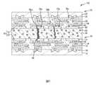
図1は、実施例1に係る半導体装置100の断面図である。図1のように、実施例1の半導体装置100は、半導体チップ10、半導体チップ30、及び中間膜50、を備える。 FIG. 1 is a cross-sectional view of the
半導体チップ10は、基板12と絶縁膜14を有し、例えばLSI(Large Scale Integration)などのIC(Integrated Circuit)チップである。基板12は、例えばシリコン(Si)基板であり、1又は複数のトランジスタなどを含む複数の半導体素子16が形成されている。絶縁膜14は、基板12の半導体素子16が形成された側の面に設けられている。絶縁膜14内には、複数の配線層18、複数のビア配線20、及び複数の電極22が設けられている。半導体素子16は、配線層18及びビア配線20を介して、電極22に接続されている。電極22は、絶縁膜14の中間膜50が固着した面に露出している。 The
絶縁膜14は、例えば酸化シリコン(SiO2)膜などの無機絶縁膜であるが、樹脂膜などの有機絶縁膜であってもよい。配線層18、ビア配線20、及び電極22は、例えば銅(Cu)などの金属で形成されている。The
半導体チップ30は、基板32と絶縁膜34を有し、例えばLSIなどのICチップである。基板32は、例えばシリコン(Si)基板であり、1又は複数のトランジスタなどを含む複数の半導体素子36が形成されている。絶縁膜34は、基板32の半導体素子36が形成された側の面に設けられている。絶縁膜34内には、複数の配線層38、複数のビア配線40、及び複数の電極42が設けられている。半導体素子36は、配線層38及びビア配線40を介して、電極42に接続されている。電極42は、絶縁膜34の中間膜50が固着した面に露出している。 The
絶縁膜34は、例えば酸化シリコン(SiO2)膜などの無機絶縁膜であるが、樹脂膜などの有機絶縁膜であってもよい。配線層38、ビア配線40、及び電極42は、例えば銅(Cu)などの金属で形成されている。The
中間膜50は、半導体チップ10の複数の電極22が形成された面と半導体チップ30の複数の電極42が形成された面との間に挟まれて設けられ、半導体チップ10と半導体チップ30とを接着させている。中間膜50は、樹脂膜などの有機系接着剤からなり、例えばBCB(Benzocyclobutene)膜である。なお、中間膜50は、無機膜であってもよい。中間膜50は、内部に金属ナノ粒子52を含有する。金属ナノ粒子52の大きさは、例えば数nm〜数十nmである。 The
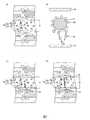
半導体チップ10の電極22と半導体チップ30の電極42とが対となって複数の電極対70が形成されている。複数の電極対70は、中間膜50に含まれる金属ナノ粒子52を構成する金属原子54が樹枝状晶の金属組織として成長したデンドライト構造体56によって接続される。ここで、電極対70がデンドライト構造体56で接続されるメカニズムを説明する。 The
図2(a)から図2(d)は、電極対70がデンドライト構造体56で接続されるメカニズムを説明する図である。図2(a)及び図2(b)のように、水分と金属ナノ粒子52が存在する中間膜50では金属ナノ粒子52を構成する金属原子が金属イオン58として抜け出して水酸化物イオン60と結合して水酸化物を形成する。金属原子は水酸化物から分離し易いため、電極対70に電位差(例えば電極22が陰極、電極42が陽極)が生じていると、金属イオン58は陰極である電極22側に引き寄せられるようになる。このように、金属ナノ粒子52を含有する中間膜50は、完全な絶縁体膜ではなく、電極対70に電位差が生じている場合は微弱な電流を流す高抵抗膜(非絶縁体膜)である。 FIG. 2A to FIG. 2D are diagrams illustrating a mechanism in which the
図2(c)のように、電極22(陰極)側に引き寄せられた金属イオン58は、電極22から電子を受け取って金属原子54となって電極22の表面に析出していく。これにより、電極22側から電極42(陽極)側に向かって、金属ナノ粒子52を構成する金属原子54が樹枝状晶の金属組織として成長していく。図2(d)のように、電極22と電極42の間を金属原子54が樹枝状晶の金属組織として成長することで、電極22と電極42(電極対70)がデンドライト構造体56で接続されるようになる。デンドライト構造体56は、例えば太さが0.1μm以下であるため、微細な電極間接続が可能となる。 As shown in FIG. 2C, the
金属ナノ粒子52から金属イオン58が抜け出すことでデンドライト構造体56が形成されることから、金属ナノ粒子52はイオン化傾向の高い金属であることが好ましい。例えば、金属ナノ粒子52は、マグネシウム(Mg)、アルミニウム(Al)、亜鉛(Zn)、鉄(Fe)、ニッケル(Ni)、錫(Sn)、又は銅(Cu)のいずれかからなることが好ましい。金属ナノ粒子52は、マグネシウム(Mg)、アルミニウム(Al)、亜鉛(Zn)、又は鉄(Fe)のいずれかからなることがより好ましく、マグネシウム(Mg)からなることが更に好ましい。 Since the
図1のように、複数の電極対70は、デンドライト構造体56による接続状態が異なる電極対を含む。これは、複数の電極対70の抵抗を異ならせることが望まれることがあるためである。例えば、半導体装置100でニューラルネットワークを構成する場合に、ニューロン素子(半導体素子16、36)間の重み付けをデンドライト構造体56の抵抗で実現する場合などである。例えば、ニューロン素子間の重みが大きい電極対70aは、太いデンドライト構造体56aで接続される。ニューロン素子間の重みが電極対70aよりも小さい電極対70bは、デンドライト構造体56aよりも細いデンドライト構造体56bで接続される。ニューロン素子間の重みが極めて小さい電極対70cは、デンドライト構造体56で接続されない。 As shown in FIG. 1, the plurality of electrode pairs 70 include electrode pairs having different connection states by the
図3(a)から図4(b)は、実施例1に係る半導体装置100の製造方法を示す断面図である。図3(a)のように、半導体素子16が形成された基板12と、配線層18、ビア配線20、及び電極22が設けられた絶縁膜14と、を備える半導体チップ10を準備する。電極22の上面は例えば1辺が0.3μm程度の正方形であり、電極22のピッチ間隔(中心間距離)は例えば0.5μm程度である。電極22は、例えば絶縁膜14にフォトリソグラフィ法及びエッチング法を用いて形成した凹部に蒸着法を用いて金属膜を埋め込むことで形成される。 FIGS. 3A to 4B are cross-sectional views illustrating the method for manufacturing the
図3(b)のように、半導体素子36が形成された基板32と、配線層38、ビア配線40、及び電極42が設けられた絶縁膜34と、を備える半導体チップ30を準備する。電極42の上面は例えば1辺が0.3μm程度の正方形であり、電極42のピッチ間隔(中心間距離)は例えば0.5μm程度である。電極42は、例えば絶縁膜34にフォトリソグラフィ法及びエッチング法を用いて形成した凹部に蒸着法を用いて金属膜を埋め込むことで形成される。 As shown in FIG. 3B, a
図3(c)のように、半導体チップ10の電極22が設けられた面に、金属ナノ粒子52を含有する中間膜50を形成する。金属ナノ粒子52は例えば銅(Cu)ナノ粒子であり、中間膜50は例えばBCB膜である。金属ナノ粒子52の大きさは例えば数nm〜数十nmで、中間膜50中の金属ナノ粒子52の含有率は例えば体積比で40%である。中間膜50は、半導体チップ10の電極22が露出する面に例えば1μm厚の樹脂フィルムを貼り付けることで形成してもよいし、スピンコート法又はスプレーコート法によって樹脂を塗布することで形成してもよい。なお、図3(c)では、半導体チップ10の電極22が設けられた面に中間膜50を形成する場合を例に示したが、半導体チップ30の電極42が設けられた面に中間膜50を形成してもよい。 As shown in FIG. 3C, the
図4(a)のように、半導体チップ10の電極22が設けられた面と半導体チップ30の電極42が設けられた面とで中間膜50を挟んだ状態とし、この状態で中間膜50を200℃に加熱する。BCB膜は熱硬化性樹脂であることから、半導体チップ10と半導体チップ30で中間膜50を挟んだ状態で中間膜50を200℃に加熱することで、半導体チップ10と半導体チップ30が中間膜50によって接着される。なお、半導体チップ10と半導体チップ30で中間膜50を挟む際の、半導体チップ10と半導体チップ30のアライメント精度は2μm程度であった。 As shown in FIG. 4A, the
図4(b)のように、電極22と電極42で形成される複数の電極対70が所望の接続状態になるよう、複数の電極対70に電圧を印加する。図2(a)から図2(d)で説明したように電極対70に電位差が生じることで電極対70はデンドライト構造体56で接続されることから、電極対70に電圧を印加することで電極対70をデンドライト構造体56で接続させることができる。このときに、デンドライト構造体56は電極間の積算電荷量が多いほどより早く成長することから、電極対70に印加する電圧の大きさに応じてデンドライト構造体56の太さを異ならせることができる。つまり、電極対70に印加する電圧の大きさに応じて、複数の電極対70の抵抗を異ならせることができる。 As shown in FIG. 4B, a voltage is applied to the plurality of electrode pairs 70 so that the plurality of electrode pairs 70 formed by the
上述したように、複数の電極対70の抵抗を異ならせることが望まれることがある。例えば、半導体装置100でニューラルネットワークを構成する場合に、ニューロン素子(半導体素子16、36)間の重み付けをデンドライト構造体56の抵抗で実現したい場合などである。例えば、ニューロン素子間の重みを大きくする電極対70aには、太いデンドライト構造体56aが形成されるように大きな電圧を印加する。ニューロン素子間の重みを電極対70aよりも小さくする電極対70bには、デンドライト構造体56aよりも細いデンドライト構造体56bが形成されるように電極対70aよりも小さな電圧を印加する。ニューロン素子間の重みを極めて小さくする電極対70cには、デンドライト構造体56が形成されないように0Vの電圧を印加する。このように、複数の電極対70のうちの少なくとも2つの電極対70に異なる電圧を印加して、複数の電極対70それぞれが所望の接続状態になるようにする。 As described above, it may be desirable to make the resistances of the plurality of electrode pairs 70 different. For example, when a neural network is configured with the
実施例1によれば、図1のように、半導体チップ10と半導体チップ30の間に金属ナノ粒子52を含有する中間膜50が設けられている。そして、複数の電極対70のうちの電極対70aは金属ナノ粒子52を構成する金属で形成されたデンドライト構造体56aで接続されている。電極対70bはデンドライト構造体56aと異なる太さのデンドライト構造体56bで接続され、電極対70cはデンドライト構造体56で接続されていない。これにより、複数の電極対70の抵抗を容易に異ならせることができる。よって、例えば半導体装置100でニューラルネットワークを構成する場合に、ニューロン素子(半導体素子16、36)間の重みをデンドライト構造体56の抵抗で容易に実現することができる。 According to the first embodiment, as shown in FIG. 1, the
また、実施例1によれば、図4(a)のように、半導体チップ10の電極22が設けられた面と半導体チップ30の電極42が設けられた面とで金属ナノ粒子52を含有する中間膜50を挟む。その後、図4(b)のように、複数の電極対70のうちの少なくとも2つの電極対70に異なる大きさの電圧を印加する。これにより、複数の電極対70の抵抗を容易に異ならせることができる。 Moreover, according to Example 1, as shown in FIG. 4A, the
図5は、実施例1の半導体装置100を動作させることによるデンドライト構造体56の変化を説明する図である。上述したように、デンドライト構造体56は電極間の積算電荷量によって変化する。言い換えると、デンドライト構造体56は電極対70a〜70cに接続された半導体素子16、36の間の信号のやり取り(電極対の使用頻度)に応じて変化する。したがって、使用頻度が高い電極対70aは太いデンドライト構造体56aで接続される。使用頻度が電極対70aよりも少ない電極対70bはデンドライト構造体56aよりも細いデンドライト構造体56bで接続される。使用頻度が極めて少ない(例えばある期間ほとんど使用されていない)電極対70cはデンドライト構造体56で接続されない。 FIG. 5 is a diagram illustrating a change in the
このように、複数の電極対70は、半導体チップ10及び半導体チップ30の動作に伴って複数の電極対70を流れる電流量に応じてデンドライト構造体56による接続が変化する。これにより、例えばニューラルネットワークにおけるニューロン素子(半導体素子16、36)間の重みの変化をデンドライト構造体56で容易に実現することができる。なお、図5において電極対70bの使用頻度が極めて少なくなると、電極対70bを接続していたデンドライト構造体56bは消滅し、デンドライト構造体56bを形成していた金属原子54は他の電極対70に供給されるようになる。 Thus, the connection of the plurality of electrode pairs 70 by the
図6は、比較例に係る半導体装置の断面図である。図6のように、比較例の半導体装置500は、半導体チップ10の電極22と半導体チップ30の電極42が直接接合されている。なお、半導体チップを金属(例えば銅(Cu))ピラーで直接接合することが知られているが、金属ピラーのピッチ間隔は5μm程度が製造的に限界とされているため、端子密度を大きくすることが難しい。一方、電極22及び電極42は、フォトリソグラフィ法などを用いて形成されるため、1μm以下の大きさ及び間隔で形成することができる。しかしながら、半導体チップ10と半導体チップ30のアライメント精度を1μm以下で行うことは難しく、図6のように、電極22と電極42に位置ずれが生じてしまう。位置ずれが生じると、電極22と電極42の接続抵抗の増大や電極22と電極42が電気的に接続しないなどの接続不良が発生してしまう。 FIG. 6 is a cross-sectional view of a semiconductor device according to a comparative example. As shown in FIG. 6, in the
これに対し、実施例1では、電極22と電極42はデンドライト構造体56で電気的に接続されているため、半導体チップ10と半導体チップ30のアライメント精度が悪い場合でも、接続不良の発生を抑制できる。 On the other hand, in Example 1, since the
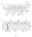
図7(a)は、実施例2に係る記憶装置を示す図、図7(b)は、図7(a)のA−A間の断面図である。なお、図7(a)では、図の明瞭化のために、中間膜90の図示は省略している。図7(a)及び図7(b)のように、実施例2の記憶装置200は、複数のワード線80と、複数のビット線82と、複数のワード線80と複数のビット線82との交差位置に配置された複数のメモリセル84と、を備える。 FIG. 7A is a diagram illustrating the storage device according to the second embodiment, and FIG. 7B is a cross-sectional view taken along the line AA in FIG. 7A. In FIG. 7A, the
複数のメモリセル84それぞれは、ワード線80に接続された電極86と、ビット線82に接続された電極88と、を備える。電極86及び電極88は、複数のメモリセル84毎に分離して設けられている。すなわち、1つのメモリセル84の電極86及び電極88は、他のメモリセル84の電極86及び電極88と接続されずに分離されている。 Each of the plurality of
複数のメモリセル84は、複数のメモリセル84で共有する中間膜90を備える。中間膜90は、複数のメモリセル84それぞれの電極86と電極88の間に位置して設けられている。中間膜90は、金属ナノ粒子92を含有する。ワード線80とビット線82によって電極86と電極88の間に電圧が印加されたメモリセル84aは、実施例1の図2で説明したように、電極86と電極88がデンドライト構造体96で接続される。一方、電極86と電極88との間に電圧が印加されていないメモリセル84b、84cは、デンドライト構造体96で接続されない。 The plurality of
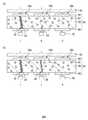
図8(a)から図8(c)は、実施例2に係る記憶装置の書き込み動作を説明する図である。図8(a)のように、初期状態においては、メモリセル84a〜84cの全てで電極86と電極88がデンドライト構造体96で接続されていない。電極86と電極88がデンドライト構造体96で接続されてなく乖離した状態を「0」のデータが書き込まれた状態とする。 FIG. 8A to FIG. 8C are diagrams for explaining the write operation of the storage device according to the second embodiment. As shown in FIG. 8A, in the initial state, the
図8(b)のように、ワード線80とビット線82によってメモリセル84aの電極86と電極88の間に電圧が印加されると、実施例1の図2で説明したように、金属ナノ粒子92を構成する金属原子94が樹枝状晶の金属組織として成長していく。図8(c)のように、電極88と電極86の間を金属原子94が樹枝状晶の金属組織として成長することで、電極86と電極88がデンドライト構造体96によって接続される。電極86と電極88がデンドライト構造体96で接続されて結合された状態を「1」のデータが書き込まれた状態とする。 As shown in FIG. 8B, when a voltage is applied between the
このように、実施例2の記憶装置200は、電極86と電極88の間のデンドライト構造体96による接続に応じて「0」又は「1」のデータが書き込まれる抵抗変化型(状態変化型)のメモリである。なお、電極86と電極88がデンドライト構造体96で接続された後において、全てのワード線80及び全てのビット線82に電圧が印加されなくなると、デンドライト構造体96はそのままの形状を維持する。したがって、実施例2の記憶装置200は、待機電源が不要な不揮発性メモリである。 As described above, the
図9(a)及び図9(b)は、実施例2に係る記憶装置の書き換え動作を説明する図である。図9(a)のように、ワード線80とビット線82によってメモリセル84bの電極86と電極88の間に電圧が印加されると、メモリセル84bにおいて金属ナノ粒子92を構成する金属原子94が樹枝状晶の金属組織として成長していく。図9(b)のように、メモリセル84bにおいて、電極88と電極86の間を金属原子94が樹枝状晶の金属組織として成長することで、電極86と電極88がデンドライト構造体96によって接続される。これにより、メモリセル84bは、「0」のデータから「1」のデータに書き換えられる。このように、電極86と電極88の間に電圧を印加する又は印加していた電圧を解除することで、メモリセル84へのデータの書き換えができる。 FIG. 9A and FIG. 9B are diagrams illustrating the rewrite operation of the storage device according to the second embodiment. As shown in FIG. 9A, when a voltage is applied between the
実施例2によれば、複数のメモリセル84は、ワード線80に接続された電極86と、ビット線82に接続された電極88と、電極86と電極88の間に設けられ、金属ナノ粒子92を含有する中間膜90と、を備える。そして、複数のメモリセル84は、ワード線80及びビット線82によって電極86と電極88の間に電圧が印加されることで、電極86と電極88がデンドライト構造体96で接続される。これにより、デンドライト構造体96の接続に応じて「0」又は「1」のデータが書き込まれる抵抗変化型のメモリを実現することができる。 According to the second embodiment, the plurality of
また、実施例2によれば、使用頻度が高い状態から低い状態に変化したメモリセル84のデンドライト構造体96は徐々に消滅するようになる。このため、実施例2の記憶装置200は学習メモリに応用することができる。また、メモリセル84の使用頻度によってデンドライト構造体96の太さなどが変化することから、抵抗値の大きさによるメモリ階層の増大を実現することもできる。 In addition, according to the second embodiment, the
以上、本発明の実施例について詳述したが、本発明はかかる特定の実施例に限定されるものではなく、特許請求の範囲に記載された本発明の要旨の範囲内において、種々の変形・変更が可能である。 Although the embodiments of the present invention have been described in detail above, the present invention is not limited to such specific embodiments, and various modifications and changes can be made within the scope of the gist of the present invention described in the claims. It can be changed.
なお、以上の説明に関して更に以下の付記を開示する。
(付記1)複数の第1電極を有する第1半導体チップと、前記複数の第1電極と複数の電極対を形成する複数の第2電極を有する第2半導体チップと、前記第1半導体チップの前記複数の第1電極が設けられた面と前記第2半導体チップの前記複数の第2電極が設けられた面との間に挟まれ、金属粒子を含有する中間膜と、を備え、前記複数の電極対のうちの第1電極対は前記金属粒子を構成する金属で形成されたデンドライト構造体で接続され、第2電極対は前記デンドライト構造体で接続されていない又は前記第1電極対を接続する前記デンドライト構造体とは異なる太さの前記デンドライト構造体で接続されている、半導体装置。
(付記2)前記複数の電極対のうちの前記第1電極対と前記第2電極対は異なる太さの前記デンドライト構造体で接続され、第3電極対は前記デンドライト構造体で接続されていない、付記1記載の半導体装置。
(付記3)前記複数の電極対は、前記第1半導体チップ及び前記第2半導体チップの動作に伴う前記複数の電極対の電流量に応じて前記デンドライト構造体による接続が変化する、付記1または2記載の半導体装置。
(付記4)前記金属粒子は、マグネシウム、アルミニウム、亜鉛、鉄、ニッケル、錫、又は銅のいずれかからなる、付記1から3のいずれか一項記載の半導体装置。
(付記5)前記中間膜は非絶縁体である、付記1から4のいずれか一項記載の半導体装置。
(付記6)複数のワード線と、複数のビット線と、前記複数のワード線と前記複数のビット線の交差位置に配置された複数のメモリセルと、を備え、前記複数のメモリセルは、前記複数のワード線及び前記複数のビット線にそれぞれ接続する第1電極及び第2電極と、前記第1電極と前記第2電極との間に設けられ、金属粒子を含有する中間膜と、を備え、前記複数のワード線及び前記複数のビット線によって前記第1電極と前記第2電極の間に電圧が印加されることで前記第1電極と前記第2電極が前記金属粒子を構成する金属で形成されたデンドライト構造体で接続される、記憶装置。
(付記7)前記第1電極及び前記第2電極は前記複数のメモリセル毎に分離して設けられ、前記中間膜は前記複数のメモリセルで共有して設けられている、付記6記載の記憶装置。
(付記8)複数の第1電極を有する第1半導体チップの前記複数の第1電極が設けられた面と、複数の第2電極を有する第2半導体チップの前記複数の第2電極が設けられた面と、で金属粒子を含有する中間膜を挟む工程と、前記中間膜を挟む工程の後、前記複数の第1電極と前記複数の第2電極とで形成される複数の電極対のうちの少なくとも2つの電極対に異なる大きさの電圧を印加する工程と、を備える半導体装置の製造方法。In addition, the following additional notes are disclosed regarding the above description.
(Supplementary Note 1) A first semiconductor chip having a plurality of first electrodes, a second semiconductor chip having a plurality of second electrodes forming a plurality of electrode pairs with the plurality of first electrodes, and the first semiconductor chip An intermediate film sandwiched between a surface provided with the plurality of first electrodes and a surface provided with the plurality of second electrodes of the second semiconductor chip and containing metal particles, Of the electrode pairs, the first electrode pair is connected by a dendrite structure formed of a metal constituting the metal particles, and the second electrode pair is not connected by the dendrite structure or the first electrode pair A semiconductor device connected by the dendrite structure having a thickness different from that of the dendrite structure to be connected.
(Appendix 2) Of the plurality of electrode pairs, the first electrode pair and the second electrode pair are connected by the dendrite structure having different thicknesses, and the third electrode pair is not connected by the dendrite structure. The semiconductor device according to
(Supplementary note 3) The connection of the plurality of electrode pairs is changed by the dendrite structure according to the amount of current of the plurality of electrode pairs accompanying the operation of the first semiconductor chip and the second semiconductor chip. 2. The semiconductor device according to 2.
(Additional remark 4) The said metal particle is a semiconductor device as described in any one of
(Supplementary note 5) The semiconductor device according to any one of
(Supplementary Note 6) A plurality of word lines, a plurality of bit lines, and a plurality of memory cells arranged at intersections of the plurality of word lines and the plurality of bit lines, the plurality of memory cells, A first electrode and a second electrode connected to the plurality of word lines and the plurality of bit lines, respectively, and an intermediate film provided between the first electrode and the second electrode and containing metal particles; A metal in which the first electrode and the second electrode constitute the metal particles by applying a voltage between the first electrode and the second electrode by the plurality of word lines and the plurality of bit lines. A storage device connected by a dendrite structure formed in
(Supplementary note 7) The memory according to supplementary note 6, wherein the first electrode and the second electrode are provided separately for each of the plurality of memory cells, and the intermediate film is provided shared by the plurality of memory cells. apparatus.
(Supplementary Note 8) The surface of the first semiconductor chip having a plurality of first electrodes provided with the plurality of first electrodes and the plurality of second electrodes of the second semiconductor chip having a plurality of second electrodes are provided. A plurality of electrode pairs formed by the plurality of first electrodes and the plurality of second electrodes after the step of sandwiching the intermediate film containing metal particles with the surface and the step of sandwiching the intermediate film Applying a voltage having a different magnitude to at least two electrode pairs of the semiconductor device.
10 半導体チップ
12 基板
14 絶縁膜
16 半導体素子
18 配線層
20 ビア配線
22 電極
30 半導体チップ
32 基板
34 絶縁膜
36 半導体素子
38 配線層
40 ビア配線
42 電極
50 中間膜
52 金属ナノ粒子
54 金属原子
56〜56b デンドライト構造体
58 金属イオン
60 水酸化物イオン
70〜70c 電極対
80 ワード線
82 ビット線
84〜84c メモリセル
86 電極
88電極
90 中間膜
92 金属ナノ粒子
94 金属原子
96 デンドライト構造体
100 半導体装置
200 記憶装置DESCRIPTION OF
Claims (6)
Translated fromJapanese前記複数の第1電極と複数の電極対を形成する複数の第2電極を有する第2半導体チップと、
前記第1半導体チップの前記複数の第1電極が設けられた面と前記第2半導体チップの前記複数の第2電極が設けられた面との間に挟まれ、金属粒子を含有する中間膜と、を備え、
前記複数の電極対のうちの第1電極対は前記金属粒子を構成する金属で形成されたデンドライト構造体で接続され、第2電極対は前記デンドライト構造体で接続されていない又は前記第1電極対を接続する前記デンドライト構造体とは異なる太さの前記デンドライト構造体で接続されている、半導体装置。A first semiconductor chip having a plurality of first electrodes;
A second semiconductor chip having a plurality of second electrodes forming a plurality of electrode pairs with the plurality of first electrodes;
An intermediate film sandwiched between a surface of the first semiconductor chip provided with the plurality of first electrodes and a surface of the second semiconductor chip provided with the plurality of second electrodes; With
The first electrode pair of the plurality of electrode pairs is connected by a dendrite structure formed of a metal constituting the metal particles, and the second electrode pair is not connected by the dendrite structure or the first electrode A semiconductor device connected by the dendrite structure having a thickness different from that of the dendrite structure connecting the pair.
複数のビット線と、
前記複数のワード線と前記複数のビット線の交差位置に配置された複数のメモリセルと、を備え、
前記複数のメモリセルは、前記複数のワード線及び前記複数のビット線にそれぞれ接続する第1電極及び第2電極と、前記第1電極と前記第2電極との間に設けられ、金属粒子を含有する中間膜と、を備え、前記複数のワード線及び前記複数のビット線によって前記第1電極と前記第2電極の間に電圧が印加されることで前記第1電極と前記第2電極が前記金属粒子を構成する金属で形成されたデンドライト構造体で接続される、記憶装置。Multiple word lines,
Multiple bit lines,
A plurality of memory cells disposed at intersections of the plurality of word lines and the plurality of bit lines;
The plurality of memory cells are provided between a first electrode and a second electrode connected to the plurality of word lines and the plurality of bit lines, respectively, and between the first electrode and the second electrode. An intermediate film containing the first electrode and the second electrode by applying a voltage between the first electrode and the second electrode by the plurality of word lines and the plurality of bit lines. A storage device connected by a dendrite structure formed of a metal constituting the metal particles.
前記中間膜を挟む工程の後、前記複数の第1電極と前記複数の第2電極とで形成される複数の電極対のうちの少なくとも2つの電極対に異なる大きさの電圧を印加する工程と、を備える半導体装置の製造方法。A surface of the first semiconductor chip having a plurality of first electrodes provided with the plurality of first electrodes; a surface of the second semiconductor chip having a plurality of second electrodes provided with the plurality of second electrodes; Sandwiching an intermediate film containing metal particles with,
Applying a voltage of a different magnitude to at least two of the plurality of electrode pairs formed by the plurality of first electrodes and the plurality of second electrodes after the step of sandwiching the intermediate film; A method for manufacturing a semiconductor device.
Priority Applications (1)
| Application Number | Priority Date | Filing Date | Title |
|---|---|---|---|
| JP2017104813AJP6870476B2 (en) | 2017-05-26 | 2017-05-26 | Semiconductor devices and methods for manufacturing semiconductor devices |
Applications Claiming Priority (1)
| Application Number | Priority Date | Filing Date | Title |
|---|---|---|---|
| JP2017104813AJP6870476B2 (en) | 2017-05-26 | 2017-05-26 | Semiconductor devices and methods for manufacturing semiconductor devices |
Publications (2)
| Publication Number | Publication Date |
|---|---|
| JP2018200951Atrue JP2018200951A (en) | 2018-12-20 |
| JP6870476B2 JP6870476B2 (en) | 2021-05-12 |
Family
ID=64668267
Family Applications (1)
| Application Number | Title | Priority Date | Filing Date |
|---|---|---|---|
| JP2017104813AActiveJP6870476B2 (en) | 2017-05-26 | 2017-05-26 | Semiconductor devices and methods for manufacturing semiconductor devices |
Country Status (1)
| Country | Link |
|---|---|
| JP (1) | JP6870476B2 (en) |
Cited By (1)
| Publication number | Priority date | Publication date | Assignee | Title |
|---|---|---|---|---|
| JP2021082653A (en)* | 2019-11-15 | 2021-05-27 | 富士通株式会社 | Switching element and manufacturing method of switching element |
Citations (5)
| Publication number | Priority date | Publication date | Assignee | Title |
|---|---|---|---|---|
| US20040193558A1 (en)* | 2003-03-27 | 2004-09-30 | Alex Nugent | Adaptive neural network utilizing nanotechnology-based components |
| JP2008244090A (en)* | 2007-03-27 | 2008-10-09 | Nec Corp | Switching element and method for manufacturing switching element |
| JP2012256657A (en)* | 2011-06-08 | 2012-12-27 | National Institute For Materials Science | Synapse operation element |
| CN104916776A (en)* | 2014-03-11 | 2015-09-16 | 科洛斯巴股份有限公司 | Selector device for two-terminal memory |
| JP2018166194A (en)* | 2017-03-28 | 2018-10-25 | 学校法人慶應義塾 | Crossbar structure and solution search system for optimization problem |
- 2017
- 2017-05-26JPJP2017104813Apatent/JP6870476B2/enactiveActive
Patent Citations (7)
| Publication number | Priority date | Publication date | Assignee | Title |
|---|---|---|---|---|
| US20040193558A1 (en)* | 2003-03-27 | 2004-09-30 | Alex Nugent | Adaptive neural network utilizing nanotechnology-based components |
| JP2008244090A (en)* | 2007-03-27 | 2008-10-09 | Nec Corp | Switching element and method for manufacturing switching element |
| JP2012256657A (en)* | 2011-06-08 | 2012-12-27 | National Institute For Materials Science | Synapse operation element |
| CN104916776A (en)* | 2014-03-11 | 2015-09-16 | 科洛斯巴股份有限公司 | Selector device for two-terminal memory |
| WO2015138119A1 (en)* | 2014-03-11 | 2015-09-17 | Crossbar, Inc. | Selector device for two-terminal memory |
| JP2017516293A (en)* | 2014-03-11 | 2017-06-15 | クロスバー, インコーポレイテッドCrossbar, Inc. | Selector element for 2-terminal memory |
| JP2018166194A (en)* | 2017-03-28 | 2018-10-25 | 学校法人慶應義塾 | Crossbar structure and solution search system for optimization problem |
Cited By (1)
| Publication number | Priority date | Publication date | Assignee | Title |
|---|---|---|---|---|
| JP2021082653A (en)* | 2019-11-15 | 2021-05-27 | 富士通株式会社 | Switching element and manufacturing method of switching element |
Also Published As
| Publication number | Publication date |
|---|---|
| JP6870476B2 (en) | 2021-05-12 |
Similar Documents
| Publication | Publication Date | Title |
|---|---|---|
| TWI705438B (en) | Integrated circuits including magnetic random access memory structures having reduced switching energy barriers for differential bit operation and methods for fabricating the same | |
| KR102385549B1 (en) | Semiconductor package and method of manufacturing the semiconductor package | |
| JP6112106B2 (en) | Resistance change element, semiconductor device having the resistance change element, method for manufacturing the semiconductor device, and programming method using the resistance change element | |
| US10714535B2 (en) | Resistive memory array and fabricating method thereof | |
| CN102881820B (en) | Magnetic random access memory and manufacture method thereof | |
| WO2019088001A1 (en) | Thermoelectric element, power generation device, and thermoelectric element production method | |
| CN102593141A (en) | Electric field modulation type random memory cell array and memory | |
| CN207149541U (en) | Capacitor and electronic equipment | |
| JP6798489B2 (en) | Resistance change element and manufacturing method of resistance change element | |
| TW201222793A (en) | Memory device | |
| JP6870476B2 (en) | Semiconductor devices and methods for manufacturing semiconductor devices | |
| WO2018181019A1 (en) | Semiconductor device and manufacturing method therefor | |
| JP2018093129A (en) | Semiconductor device | |
| CN109791840A (en) | Electronic component | |
| US11258008B2 (en) | Semiconductor device and manufacturing method for same | |
| US10418418B2 (en) | Storage device and production method thereof | |
| US7772035B2 (en) | Manufacturing method of semiconductor device | |
| WO2016084349A1 (en) | Variable-resistance element and method of manufacturing same, and semiconductor device | |
| JP2018147933A (en) | Manufacturing method of semiconductor device | |
| JP5446869B2 (en) | Switching element and method of manufacturing switching element | |
| US10157964B2 (en) | Memory device and method for manufacturing the same | |
| US20200020854A1 (en) | Storage device | |
| CN117042445A (en) | Memory device and method of manufacturing the same | |
| CN116249356A (en) | Integrated wafer and method for manufacturing the same | |
| JP2011258872A (en) | Semiconductor device |
Legal Events
| Date | Code | Title | Description |
|---|---|---|---|
| A621 | Written request for application examination | Free format text:JAPANESE INTERMEDIATE CODE: A621 Effective date:20200310 | |
| A977 | Report on retrieval | Free format text:JAPANESE INTERMEDIATE CODE: A971007 Effective date:20210129 | |
| A131 | Notification of reasons for refusal | Free format text:JAPANESE INTERMEDIATE CODE: A131 Effective date:20210202 | |
| A521 | Request for written amendment filed | Free format text:JAPANESE INTERMEDIATE CODE: A523 Effective date:20210224 | |
| TRDD | Decision of grant or rejection written | ||
| A01 | Written decision to grant a patent or to grant a registration (utility model) | Free format text:JAPANESE INTERMEDIATE CODE: A01 Effective date:20210316 | |
| A61 | First payment of annual fees (during grant procedure) | Free format text:JAPANESE INTERMEDIATE CODE: A61 Effective date:20210329 | |
| R150 | Certificate of patent or registration of utility model | Ref document number:6870476 Country of ref document:JP Free format text:JAPANESE INTERMEDIATE CODE: R150 | |
| R250 | Receipt of annual fees | Free format text:JAPANESE INTERMEDIATE CODE: R250 | |
| S111 | Request for change of ownership or part of ownership | Free format text:JAPANESE INTERMEDIATE CODE: R313113 |