JP2018191083A - Imaging apparatus - Google Patents
Imaging apparatusDownload PDFInfo
- Publication number
- JP2018191083A JP2018191083AJP2017090575AJP2017090575AJP2018191083AJP 2018191083 AJP2018191083 AJP 2018191083AJP 2017090575 AJP2017090575 AJP 2017090575AJP 2017090575 AJP2017090575 AJP 2017090575AJP 2018191083 AJP2018191083 AJP 2018191083A
- Authority
- JP
- Japan
- Prior art keywords
- defective pixel
- pixel data
- unit
- row
- image sensor
- Prior art date
- Legal status (The legal status is an assumption and is not a legal conclusion. Google has not performed a legal analysis and makes no representation as to the accuracy of the status listed.)
- Pending
Links
Images


Landscapes
- Transforming Light Signals Into Electric Signals (AREA)
Abstract
Description
Translated fromJapanese本発明は撮像装置に関し、特に撮像素子の欠陥画素補正を行う撮像装置に関するものである。 The present invention relates to an imaging apparatus, and more particularly to an imaging apparatus that performs defective pixel correction of an imaging element.
一般的なCMOS型の撮像素子においては、各画素からの信号の読み出し方法として行単位でリセット動作と信号出力動作を繰り返すローリングシャッタ方式が採用されている。しかし、ローリングシャッタ方式で読み出しを行うと、動きのある被写体を撮像した場合に、行単位で発生する露光期間のずれにより撮像した被写体に歪み(ローリングシャッタ歪)が生じてしまうという問題があった。 In a general CMOS type image sensor, a rolling shutter system that repeats a reset operation and a signal output operation in units of rows is adopted as a method of reading a signal from each pixel. However, when reading is performed using the rolling shutter method, there is a problem in that when a moving subject is imaged, distortion (rolling shutter distortion) occurs in the imaged subject due to a shift in the exposure period that occurs in units of rows. .
一方で、特許文献1に記載の撮像素子のように、画素内に蓄積電荷を保持するメモリを備えることで、一括でリセット動作を行う、いわゆるグローバルシャッタ方式が採用されている撮像素子も知られている。グローバルシャッタ方式を採用した撮像素子においては、全画素を一括でリセットし所定の露光期間を経た後に一括で画素内のメモリへ電荷を転送する制御と、メモリに記憶された電荷を行毎に順次読み出しを行う制御が行われる。この読み出し方法では、全画素の露光期間タイミングが一致するため、ローリングシャッタ歪みは生じない。 On the other hand, there is also known an image sensor that employs a so-called global shutter system in which a reset operation is performed in a lump by providing a memory that holds accumulated charges in a pixel as in the image sensor described in
しかしながら、特許文献1に記載の撮像素子においては、読み出し動作中に画素内のメモリに電荷を保持する期間が異なる場合がある。このメモリに電荷を保持する期間の長さに起因して、出力信号に含まれる暗電流量(欠陥画素のレベル)も変化することとなる。そのため、事前に検出した欠陥補正データからだけでは、欠陥画素のレベルを推定することが難しく、補正すべき欠陥画素を適切に補正できないという問題があった。 However, in the image sensor described in
本発明は上述した課題に鑑みてなされたものであり、その目的はグローバルシャッタ方式を採用した撮像素子を用いた場合において、良好に欠陥画素を補正することが可能な撮像装置を提供することである。 The present invention has been made in view of the above-described problems, and an object of the present invention is to provide an imaging apparatus capable of correcting defective pixels satisfactorily when an imaging element employing a global shutter system is used. is there.
本発明の撮像装置は、露光期間中に生じた電荷の蓄積を行う光電変換部と、前記電荷を保持する保持部と、前記光電変換部と前記保持部とを接続するための第1の転送スイッチと、前記保持部と転送された電荷に基づく信号を出力する増幅部とを接続するための第2の転送スイッチとをそれぞれが有する複数の画素とを有する撮像素子と、前記撮像素子から出力される画素信号に含まれる欠陥を補正する補正手段と、を有し、前記補正手段は、前記露光期間中における前記第1の転送スイッチの接続回数に応じて、補正方法を変更することを特徴とする。 The image pickup apparatus according to the present invention includes a photoelectric conversion unit that accumulates charges generated during an exposure period, a holding unit that holds the charge, and a first transfer for connecting the photoelectric conversion unit and the holding unit. An image sensor including a switch, and a plurality of pixels each having a second transfer switch for connecting the holding unit and an amplifying unit that outputs a signal based on the transferred charge, and an output from the image sensor Correcting means for correcting a defect included in the pixel signal to be corrected, wherein the correcting means changes a correction method in accordance with the number of connection times of the first transfer switch during the exposure period. And
以上説明したように、本発明によれば、グローバルシャッタ方式を採用した撮像素子を用いた場合において、良好に欠陥画素を補正することが可能な撮像装置を提供することが可能となる。 As described above, according to the present invention, it is possible to provide an imaging apparatus that can correct defective pixels satisfactorily when an imaging element employing a global shutter system is used.
発明を実施するための形態としては、まず、本発明の実施形態としてのカメラ全体の構成及びその動作を各図を用いて説明する。なお、本発明の実施形態はこれらに限られるものではなく、適宜変更が可能である。 As a mode for carrying out the invention, first, the configuration and operation of the entire camera as an embodiment of the present invention will be described with reference to the drawings. In addition, embodiment of this invention is not restricted to these, A change is possible suitably.
<第1の実施形態>
図1は、本発明の実施形態の撮像装置100の機能ブロック図である。図1において、101は被写体の光学像を形成するレンズ(撮像光学系)であり、変倍に際して光軸方向に移動する変倍レンズ(ズームレンズ)と、焦点調節(合焦)に際して光軸方向に移動するフォーカスレンズとを有する。また、レンズ101は入射光量を制御する絞りとNDを備えている。<First Embodiment>
FIG. 1 is a functional block diagram of an imaging apparatus 100 according to an embodiment of the present invention. In FIG. 1, reference numeral 101 denotes a lens (imaging optical system) that forms an optical image of a subject, a zoom lens that moves in the optical axis direction during zooming, and an optical axis direction during focus adjustment (focusing). And a focus lens that moves to the center. The lens 101 includes a diaphragm and ND that control the amount of incident light.
102はレンズ101が形成した光学像を電気信号に光電変換する撮像素子である。本実施形態において撮像素子102はCMOS型のエリアイメージセンサであり水平方向に少なくとも4000画素以上の有効画素を備えている。本実施形態の撮像素子102はグローバルシャッタ方式を用いて露光制御が可能である。なお、撮像素子102はシリコン基板上に形成されたCMOS型の撮像素子に限られるものではなく、有機膜等からなる光電変換膜を光電変換部として用いる光電変換膜型の撮像素子であってもよい。 An
103は撮像素子102から読み出された映像信号を所定のフォーマットの映像信号に変換する映像信号処理部である。映像信号処理部103には、フォーマットの変換以外にも画像の黒レベル等を補正するためのオフセット補正回路や、カラーバランス等を補正するためのゲイン補正回路等を有する。
104は撮像装置100全体を制御するための全体制御演算部である。全体制御演算部104は、各種演算と撮像装置100全体を制御するCPUを含む。当該CPUは、撮像装置100全体を制御するために各構成要素を統括的に制御する。それと共に各種設定パラメータ等の設定を各構成要素に対して行う。また、CPUは、データを電気的に書き込み・消去可能なキャッシュメモリ等を含み、これに記録されたプログラムを実行する。なお、メモリは、CPUが実行するプログラム格納領域、プログラム実行中のワーク領域、データの格納領域等として使用される。また、全体制御演算部104は、撮像素子102から出力される信号の解析や画像処理を行い、映像データを生成する機能も有する。生成された映像データはLCD等の表示部等に出力される。また、全体制御演算部104は映像信号処理部103からの出力信号より適切な露出条件を算出し、レンズ101内部にある絞りやND、また、撮像素子102でのシャッタスピード、さらに映像信号処理部103でかけるゲインの値を制御する。ここでいうシャッタスピードとは電子シャッタによる露光時間に相当する。全体制御演算部104は撮像素子102に電荷の蓄積開始タイミングと電荷の読み出しタイミング等を指示し、各構成要素の制御を行う。
105はRAMであり、全体制御演算部104の演算結果や映像信号処理部103の出力信号を一時的に記憶する。106はROMであり、欠陥画素データや種々の調整値またはパラメータを記憶する。107はDVD、ハードディスク、不揮発性メモリなどの記録媒体である。108は外部I/F部であり、撮像した映像データを外部のモニタやレコーダに出力したり、他のビデオカメラやプレーヤから映像データを入力したりできる。あるいは、外部I/F部108を介して撮像装置100は外部のコンピュータと接続し、又は直接インターネットを介して必要な情報を取得することができる。なお、外部I/F部108は有線による接続に限られず、無線LAN等の所定の規格の無線接続であってもよい。
109は欠陥画素検出部であり、RAM105等に格納された映像信号を用いて、映像信号に含まれる欠陥(欠陥画素)を検出する。検出した欠陥画素に係るデータ(欠陥画素データ)には、位置、レベル、欠陥の種類等が含まれる。それぞれの欠陥画素データはRAM105及びROM106に記憶される。110は欠陥画素補正部であり、欠陥画素検出部109で検出された欠陥画素データを用いて、補正の対象となる欠陥画素を補正する。それぞれの動作の詳細に関しては後述する。
図2は撮像素子102における単位画素の回路構成を示した図である。200はフォトダイオード(PD)であり、入射光に比例した電荷が光電変換作用により発生する。201はメモリ部(MEM)であり、入射光に対して遮光されている。PD200で発生した電荷を一時的に保持する機能を有する保持部に相当する。MEM201に電荷を一時的に保持することでグローバルシャッタ方式での読み出し動作が可能となる。202はフローティングディフュージョン(FD)であり、MEM201で発生した電荷を一時的に保持する。 FIG. 2 is a diagram illustrating a circuit configuration of a unit pixel in the
転送スイッチ203は、PD200で発生した電荷をMEM201へ転送するための転送動作を制御するためのスイッチである。転送スイッチ203を同一タイミングで制御することで本実施形態の撮像素子102は一括転送が実現可能となる。具体的には、有効画素の前面において、各画素に含まれる転送スイッチ203を制御することで、PD200で発生した電荷をMEM201へ一括して同時期に転送することが可能となる。転送スイッチ204は、MEM201で一時的に保持された電荷をFD202へ転送するための転送動作を制御するためのスイッチである。転送スイッチ204の制御を行毎に順次行うことで、画面全体から発生電荷に基づく画素信号を読み出すことが可能となる。 The
205はリセットスイッチであり、PD200、MEM201、FD202等の電荷をリセットするためのリセット動作を制御するためのスイッチである。リセットスイッチ205の一端は電源につながっており、スイッチを導通させることによって、FD202の電荷をリセットすることが可能となる。さらに、転送スイッチ203または転送スイッチ204を同時に制御することでPD200またはMEM201の電荷も同様にリセットすることができる。
206はソースフォロアアンプ(SF)であり、FD202に一時的に保持されている電荷量に基づいて、増幅された電圧信号を後段の回路へ出力する。207は行選択スイッチであり、SF206の出力信号を、画素より(SF206より)出力するかを制御する。なお、本実施形態におけるFD202及びSF206はMEM201から転送された電荷に基づく信号を出力するための増幅部に相当する。
本実施形態において撮像素子102に含まれる各画素にはPD200から行選択スイッチ207までのそれぞれ構成を含む。しかし、撮像素子102の画素構成はこれに限られるものではなく、転送スイッチ204までの構成を1画素とし、FD202以降の各構成を行方向または列方向に隣接する画素と共有する構成としてもよい。 In the present embodiment, each pixel included in the
208は垂直線であり、行選択スイッチ207で選択されたSF206の出力を後述の列アンプへ出力する。本実施形態において、垂直線208は各列ごとに一つであり、同列の画素で共有して使用する構成としているが各列に複数の垂直線208を備える構成としてもよい。209は列アンプであり、垂直線208に出力された画素からの信号を増幅する。210はAD変換回路であり、列アンプ209の出力信号を、サンプルホールドした後、AD変換を行う。AD変換回路210は、映像信号とノイズ信号を別々のタイミングでAD変換を行い、それぞれ別のメモリに一時的に格納する。その後、AD変換された映像信号からAD変換されたノイズ信号を減算した後に、後段の回路へ出力する。ここで、出力は不図示の水平走査回路によって行われ、各画素の信号はシリアル信号へと変換され順次画素信号として出力される。
撮像素子102はさらに不図示の駆動回路を備える。不図示の駆動回路は行単位で共通の出力信号線を備え、当該出力信号線を制御することによって各スイッチのON/OFF及び列アンプ209のゲイン設定、AD変換回路210の動作制御等を行うことができる。 The
また、第1の実施形態では、PD200からMEM201への転送動作を1回の露光期間中において複数回行う。特に転送動作の制御回数に応じて、補正対象とする欠陥画素を変更する例を示す。図3は、第1の実施形態における欠陥画素検出のフローチャートである。本フローチャートの動作は全体制御演算部104によって行われる。なお、実際の検出動作に関しては、全体制御演算部104によって制御される欠陥画素検出部109が行う。なお、欠陥画素を精度よく検出するために、撮像素子102に光が入射しないようにレンズ101を遮光しておくことが好ましい。 In the first embodiment, the transfer operation from the
ステップS300において、全体制御演算部104は、撮像素子102の駆動モードを設定する。具体的には、MEM201で生じた欠陥を検出する専用の駆動モードにて撮像素子102が動作するよう、駆動モード設定用のパラメータを撮像素子102に対して設定する。そして処理をステップS301に進める。 In step S300, the overall
ステップS301において、全体制御演算部104は、ステップS300にて設定した駆動モードで撮像素子102を駆動し、出力される画素信号より欠陥画素を検出する。そして、全体制御演算部104は検出結果に基づいて、第1の欠陥画素データを生成する。ここで、本実施形態の欠陥画素の検出は検出対象画素とその周辺画素との出力差によって検出を行う。特に、遮光して撮像した画像の信号量は黒レベルと略等しくなることから、周辺の画素と比較して黒レベルから出力値がかい離している画素を欠陥画素として検出する。そして、処理をステップS302に進める。 In step S301, the overall
ステップS302において、全体制御演算部104は、第1の欠陥画素データに基づいて演算(正規化)処理を行い、第2の欠陥画素データを生成する。本演算動作に関する詳細は、後述する。そして、処理をステップS303に進める。 In step S302, the overall
ステップS303において、全体制御演算部104は、撮像素子102を所定の駆動モードに戻し、本フローチャートの処理を終了する。ここで、所定の駆動モードとは動画像を取得するためのモードであり、たとえば4Kまたは8K動画を撮像するためのモードやダイナミックレンジ拡大動画を撮像するためのモード等が挙げられる。なお、欠陥画素の検出のみを目的とする場合は、駆動モードの設定は行わずに通電状態をOFFとする動作としてもよい。なお、ステップS300において、欠陥を検出するための専用の駆動モードにて撮像素子102を動作させる例を示したが、通常の動画撮影を行うモード等を利用するようにしてもよい。 In step S303, the overall
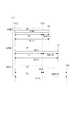
図4は、ステップS300におけるMEM201で生じた欠陥を検出するための撮像素子102を駆動するタイミングを示した図である。横軸は経過時間であり、特定のタイミングに関しては点線で示している。なお、代表して先頭行である0行目と、最終行であるN行目と、その中間位置に位置するk行目の3行分のタイミングを示している。なお、本動作は不図示の垂直同期信号に同期して開始され、各行個別の動作は不図示の水平同期信号によって制御される。それぞれの信号は全体制御演算部104より撮像素子102に供給される。また、本実施形態において、撮像素子102の各行に含まれる画素は不図示の駆動回路によって同一タイミングで制御される。したがって、k行目のタイミングではk行目に含まれるすべての画素が同一のタイミングで垂直線208に読み出されてAD変換される。 FIG. 4 is a diagram illustrating timing for driving the
T401では、0行目からN行目までの全行に対して同時に一括してPD200のリセット動作を行う。なお、本リセット動作に伴いMEM201及びFD202も同時にリセットされる。本リセット動作の終了からPD200において電荷の蓄積が開始される。 In T401, the
T402では、0行目からN行目までの全画素に対して同時に一括してMEM201をリセットする。T403では、0行目からN行目までの全画素に対してPD200の蓄積を終了するが、従来の動作とは異なり、転送スイッチ203を制御することは行わず、PD200からMEM201への電荷の転送は行わない。 At T402, the
T404では、0行目のMEM201に保持していた電荷を後段の回路へ読み出す。T405では、k行目のMEM201に保持していた電荷を後段の回路へ読み出す。T406では、N行目のMEM201に保持していた電荷を後段の回路へ読み出す。このように先頭行より順次MEM201からの転送を行う。この際、T402からT403までの時間をtFL、T403からT404までの時間をtMdiff(0)、T403からT406までの時間をtMdiff(N)と定義する。この場合、k行目のMEM201における電荷の保持時間tM(k)は、以下の式で算出できる。
tM(k)= tFL
+((tMdiff(N)−tMdiff(0))/N)x k
+ tMdiff(0)In T404, the charge held in the
tM (k) = tFL
+ ((TMdiff (N) −tMdiff (0)) / N) x k
+ TMdiff (0)
すでに述べたが、本読み出し方法では、MEM201の欠陥をより精度よく検出するために、PD200で生じた電荷の転送は行わない。また、MEM201で生じる欠陥を強調するために、電荷を保持する保持時間であるtFLは可能な範囲で長くしておくことが望ましい。 As described above, in this reading method, the charge generated in the
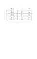
図5はステップS301で生成する第1の欠陥画素データの一例を示した図である。第1の欠陥画素データはアドレス、レベル、種類の3つの要素で構成されている。 FIG. 5 is a diagram showing an example of the first defective pixel data generated in step S301. The first defective pixel data is composed of three elements: address, level, and type.
ここで、アドレスとは、撮像素子102における対象画素の座標情報であり、水平アドレス(X)と垂直アドレス(Y)の2次元アドレスを用いて表される。なお、2次元アドレスでなくとも、読み出し順番(画像の左上(最初に読み出される画素)から数えた画素数の相対値)である1次元アドレスを用いてもよい。レベルとは、着目画素のレベルと周囲画素のメディアン値もしくは平均値との差の情報である。レベルが高い場合は出力信号としては大きくなる。つまり、欠陥としては大きい欠陥となる。種類は、欠陥画素の種類であり、どのような特性を持った欠陥であるかといった情報を記憶する。たとえば、撮像素子102のどの構成要素で発生した欠陥かを判別するために用いられる。これはPD200で発生した欠陥かMEM201で発生した欠陥かによって補正すべき条件が異なるためであり、適切に欠陥を補正等を行うためには種類の情報を用いて適切に判断する必要がある。たとえば、PD200で生じた欠陥画素はK1、MEM201で生じた欠陥画素はK2、という情報を記憶する。図4で示した駆動モードで撮像素子102を駆動することによって各画素におけるMEM201の欠陥を検出することが可能となる。そのため、本駆動モードで検出した欠陥に対してはK2の種類を付与する。なお、PD200で生じた欠陥画素の検出方法に関しては、従来同様であるので、その説明を省略する。なお、同一の駆動モードで複数種類の欠陥を検出するようにしてもよい。 Here, the address is coordinate information of the target pixel in the
図6はステップS302で生成する第2の欠陥画素データの一例を示した図である。第2の欠陥画素データは第1の欠陥画素データ同様、アドレス、レベル、種類から構成されており、データ数も第1の欠陥画素データと同じである。そして、ステップS302では、第2の欠陥画素データのアドレスと種類には、第1の欠陥画素データのアドレスと種類と同じ情報が格納される。 FIG. 6 is a diagram showing an example of second defective pixel data generated in step S302. Similar to the first defective pixel data, the second defective pixel data includes an address, a level, and a type, and the number of data is the same as that of the first defective pixel data. In step S302, the same information as the address and type of the first defective pixel data is stored in the address and type of the second defective pixel data.
ここで、第2の欠陥画素データのレベルのうち、種類がK1(K2以外)であるものについては、第1の欠陥画素データと同じ値を格納する。一方で、第2の欠陥画素データのレベルのうち、種類がK2であるものは、第1の欠陥画素データのレベルを正規化した値を格納する。第1の欠陥画素データにおけるレベルをLn、正規化後の電荷保持時間をtREF、欠陥画素の垂直アドレスをYnとすると、正規化後のレベルLn_REFは、以下の式で求める。
Ln_REF = Ln x tREF / tM(Yn)Here, among the levels of the second defective pixel data, those having the type K1 (other than K2) store the same value as the first defective pixel data. On the other hand, among the levels of the second defective pixel data, those whose type is K2 stores a value obtained by normalizing the level of the first defective pixel data. When the level in the first defective pixel data is Ln, the normalized charge retention time is tREF, and the vertical address of the defective pixel is Yn, the normalized level Ln_REF is obtained by the following equation.
Ln_REF = Ln × tREF / tM (Yn)
本実施形態の撮像素子102はグローバルシャッタ方式の読み出し動作を行うために、図4で示すようにMEM201をリセットするタイミングはT402で同一であるが、MEM201をリセットしてから信号を読み出すまでの時間が行ごとに異なる。そのため、MEM201で欠陥が発生した場合には、どの行で発生したかによって欠陥のレベルが異なることとなる。具体的には、同程度のレベルであっても先頭行で発生するか最終行で発生するかで、図3のステップS301において検出されるレベルは異なることとなる。この変化するレベルはtM(k)の値に略比例するため、垂直アドレスの値によって正規化することで、読み出し順番に依存しないレベルとなる。なお、ステップS302で生成した第2の欠陥画素データは、RAM105およびROM106に記憶される。 Since the
図7は、第1の実施形態における欠陥画素補正処理のフローチャートである。本フローチャートの動作は全体制御演算部104によって行われる。なお、実際の補正動作に関しては、全体制御演算部104によって制御される欠陥画素補正部110が行う。 FIG. 7 is a flowchart of defective pixel correction processing in the first embodiment. The operation of this flowchart is performed by the overall
ステップS700において、全体制御演算部104は、所定の駆動モード(例えば動画像取得用の駆動モード)で撮像素子102を動作し、各画素から画素信号を出力させる。そして、それぞれの画素または行に対して、露光期間中におけるPD200からMEM201への電荷の転送回数を判定する。判定結果として転送回数が2回以上の場合はステップS701へ処理を進め、そうでない場合はステップS702へ処理を進める。 In step S700, the overall
ステップS701において、全体制御演算部104は、ステップS700にて判定した転送回数及び露出条件(シャッタスピード、ISO感度・入射光量等)に応じて、補正に用いる欠陥画素データの決定及びその変更する制御を行う。欠陥画素データの変更が終了した後、ステップS703に処理を進める。 In step S701, the overall
ステップS702において、全体制御演算部104は、露出条件のみに応じて欠陥画素データを変更する。欠陥画素データの変更が終了した後、ステップS703に処理を進める。 In step S702, the overall
ステップS703において、全体制御演算部104は、ステップS701あるいはステップS702にて取得した欠陥画素データを用いて欠陥画素を補正する。本実施形態において、欠陥画素の補正には、補正対象画素が欠陥画素データを参照して補正対象画素か否かを判定する判定ステップと、補正対象画素と判定された場合に周辺画素の画素信号を用いて補間処理する補間ステップとを含む。判定ステップにおいては、補正対象画素に対応する欠陥画素データに含まれるレベルが所定の閾値を超えたか否かによって判定が行われる。 In step S703, the overall
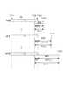
図8は、PD200からMEM201への電荷の転送回数がnTXP回(nTXP≧2)である場合の、撮像素子102の読み出しタイミングを示した図である。 FIG. 8 is a diagram illustrating the readout timing of the
T801では、0行目からN行目までの全行に対して同時に一括してPD200のリセット動作を行う。なお、本リセット動作に伴いMEM201及びFD202も同時にリセットされる。本リセット動作の終了からPD200において電荷の蓄積が開始される。 At T801, the
T802では、0行目からN行目までの全行に対して同時に一括してMEM201をリセットする。その後、PD200からMEM201への電荷の転送(1回目)を行う。 At T802, the
T803では、0行目からN行目までの全行に対して同時に一括してPD200からMEM201への電荷の転送(nTXP回目)を行い、PD200の蓄積を終了する。 At T803, charge transfer from the
ここで、T802からT803までの期間は、(T803−T802)/(nTXP−1)の時間間隔で、PD200からMEM201への電荷の転送を行う。なお、PD200からMEM201への電荷の転送タイミングは必ずしも等間隔でなくてもよい。 Here, during a period from T802 to T803, charge is transferred from the
T804乃至T806では、0行目乃至N行目のMEM201に保持していた電荷をそれぞれ順次後段の回路へ読み出す。 In T804 to T806, the charges held in the
ここで、T801からT803までの時間をtPDとすると、T802からT803までの時間は、tPDx(1−1/nTXP)である。また、T803からT804までの時間をtMdiff(0)、T803からT806までの時間をtMdiff(N)とすると、k行目のMEM201における電荷の保持時間tMm(k)は、以下の式で算出できる。
tMm(k)= tPDx(1−1/nTXP)
+((tMdiff(N)−tMdiff(0))/N)x k
+ tMdiff(0)Here, if the time from T801 to T803 is tPD, the time from T802 to T803 is tPDx (1-1 / nTXP). Further, assuming that the time from T803 to T804 is tMdiff (0) and the time from T803 to T806 is tMdiff (N), the charge retention time tMm (k) in the
tMm (k) = tPDx (1-1 / nTXP)
+ ((TMdiff (N) −tMdiff (0)) / N) x k
+ TMdiff (0)
図9は、ステップS701における変更後の欠陥画素データの一例を示した図である。すでに説明したようにステップS701における変更後の欠陥画素データも、アドレス、レベル、種類から構成されており、データ数も第2の欠陥画素データと同じである。ステップS701における変更後の欠陥画素データのアドレスと種類には、第2の欠陥画素データのアドレスと種類と同じ情報を格納する。そして、ステップS701における変更後の欠陥画素データのレベルのうち、種類がK1であるものについては、第2の欠陥画素データと同じ値を格納する。最後に、ステップS701における変更後の欠陥画素データのレベルのうち、種類がK2であるものは、第2の欠陥画素データのレベルを以下の式で変更した値を格納する。
Ln_m = Ln_REF x tMm(Yn)/tREFFIG. 9 is a diagram showing an example of defective pixel data after the change in step S701. As already described, the defective pixel data after the change in step S701 is also composed of an address, a level, and a type, and the number of data is the same as that of the second defective pixel data. In the address and type of the defective pixel data after the change in step S701, the same information as the address and type of the second defective pixel data is stored. Of the levels of the defective pixel data after the change in step S701, those having the type K1 store the same value as the second defective pixel data. Finally, among the levels of defective pixel data after the change in step S701, those having the type K2 store values obtained by changing the level of the second defective pixel data by the following formula.
Ln_m = Ln_REF × tMm (Yn) / tREF
ここで、Ln_mは変更後のレベル、Ln_REFは第2の欠陥画素データのレベル、tMm(k)はk行目のMEM201における電荷の保持時間、Ynは欠陥画素の垂直アドレス、tREFは正規化後の電荷保持時間である。このように、MEM201における電荷の保持時間に基づいて欠陥画素データのレベルを変更することにより、欠陥補正の対象となる画素を適切に選択することが可能となる。 Here, Ln_m is the level after change, Ln_REF is the level of the second defective pixel data, tMm (k) is the charge holding time in the
図10は、PD200からMEM201への電荷の転送回数が1回である場合の、撮像素子102の読み出しタイミングを示した図である。 FIG. 10 is a diagram illustrating the readout timing of the
T1001では、0行目からN行目までの全行に対して同時に一括してPD200をリセットを行う。なお、本リセット動作に伴いMEM201及びFD202も同時にリセットされる。本リセット動作の終了からPD200において電荷の蓄積が開始される。 In T1001, the
T1002では、0行目からN行目までの全行に対して同時に一括してMEM201のリセットを行う。 In T1002, the
T1003では、0行目からN行目までの全行に対して同時に一括してPD200からMEM201への電荷の転送を行い、PD200の蓄積を終了する。 In T1003, charges are transferred from the
T1004乃至T1006では、0行目乃至N行目のMEM201に保持していた電荷をそれぞれ順次後段の回路へ読み出す。 In T1004 to T1006, the charges held in the
ここで、T1002からT1003までの時間をtFS、T1003からT1004までの時間をtMdiff(0)、T1003からT1006までの時間をtMdiff(N)とする。この場合、k行目のMEM201における電荷の保持時間tMs(k)は、以下の式で算出できる。
tMs(k)= tFS
+((tMdiff(N)−tMdiff(0))/N)x k
+ tMdiff(0)Here, the time from T1002 to T1003 is tFS, the time from T1003 to T1004 is tMdiff (0), and the time from T1003 to T1006 is tMdiff (N). In this case, the charge retention time tMs (k) in the k-
tMs (k) = tFS
+ ((TMdiff (N) −tMdiff (0)) / N) x k
+ TMdiff (0)
図11は、ステップS702における変更後の欠陥画素データの一例を示した図である。ステップS702における変更後の欠陥画素データも、アドレス、レベル、種類から構成されており、データ数も第2の欠陥画素データと同じである。ステップS702における変更後の欠陥画素データのアドレスと種類には、第2の欠陥画素データのアドレスと種類と同じ情報を格納する。ステップS702における変更後の欠陥画素データのレベルのうち、種類がK1であるものについては、第2の欠陥画素データと同じ値を格納する。最後に、ステップS702における変更後の欠陥画素データのレベルのうち、種類がK2であるものは、第2の欠陥画素データのレベルを以下の式で変更した値を格納する。
Ln_s = Ln_REF x tMs(Yn)/tREFFIG. 11 is a diagram illustrating an example of defective pixel data after the change in step S702. The defective pixel data after the change in step S702 is also composed of an address, a level, and a type, and the number of data is the same as the second defective pixel data. The same information as the address and type of the second defective pixel data is stored in the address and type of the defective pixel data after the change in step S702. Of the levels of the defective pixel data after the change in step S702, the same value as the second defective pixel data is stored for the type of K1. Finally, among the levels of defective pixel data after the change in step S702, those whose type is K2 stores a value obtained by changing the level of the second defective pixel data by the following equation.
Ln_s = Ln_REF x tMs (Yn) / tREF
ここで、Ln_sは変更後のレベル、Ln_REFは第2の欠陥画素データのレベル、tMs(k)はk行目のMEM201における電荷の保持時間、Ynは欠陥画素の垂直アドレス、tREFは正規化後の電荷保持時間である。 Here, Ln_s is the level after change, Ln_REF is the level of the second defective pixel data, tMs (k) is the charge retention time in the
また、ステップS703での、欠陥画素の補正は、ステップS701もしくはステップS702で生成した欠陥画素データのうち、所定の閾値を超えるレベルの欠陥画素に対して補正を行う。補正方法は周辺画素を用いて、対象画素を補完する従来の欠陥画素補正方法同様であるのでその説明を省略する。 In step S703, the defective pixel is corrected by correcting defective pixels at a level exceeding a predetermined threshold in the defective pixel data generated in step S701 or step S702. Since the correction method is the same as the conventional defective pixel correction method for complementing the target pixel using peripheral pixels, the description thereof is omitted.
以上、説明したように、第1の実施形態においては、PD200からMEM201への転送回数に応じて、適切に欠陥画素を補正することが可能である。つまり、あらかじめ検出した欠陥画素の情報を用いて、転送回数が1回であれば、所定の計算により欠陥画素を推定し、補正対象となる画素を適切に選択し、補正することが可能である。そして、転送回数が2回以上の場合であれば、転送回数とシャッタスピード情報から欠陥画素レベルを推定し、補正対象となる画素を適切に選択し、補正することが可能である。これは、転送回数が上昇することでMEM201で電荷を保持する期間が長くなることから、転送スイッチの制御回数に応じて欠陥を補正する画素信号の数を増加させるように変更することとなる。これによって転送スイッチの制御回数に依存して変動する欠陥を適切に補正することが可能となる。 As described above, in the first embodiment, it is possible to appropriately correct defective pixels according to the number of transfers from the
<第2の実施形態>
第2の実施形態では、1フレームにおける読み出し開始行に応じて、補正対象とする欠陥画素を変更する例を示す。図12では、第2の実施形態における撮像素子102の読み出し領域を示す。第1の読み出しモードでは、(0,0)〜(M,N)の領域を読み出す。読み出しは、画面上部から行毎に順次読み出す(読み出し領域1201)。第2の読み出しモードでは、(C,A)〜(D,B)の領域を読み出す。読み出しは、画面上部から行毎に順次読み出す(読み出し領域1202)。なお、読み出し領域1201の領域設定は不図示のユーザーインターフェースを用いて行われる。例えば、撮像する画像のアスペクト比(例えば3:2、4:3、16:9等)を変更する動作もこれにあたる。また、ユーザーが設定するROI領域を読み出し領域1201としてもよい。<Second Embodiment>
In the second embodiment, an example in which a defective pixel to be corrected is changed in accordance with a read start row in one frame. FIG. 12 shows a readout area of the
図13は、第2の実施形態における、欠陥画素検出のフローチャートを示した図である。本フローチャートの動作は全体制御演算部104によって行われる。なお、実際の検出動作に関しては、全体制御演算部104によって制御される欠陥画素検出部109が行う。なお、欠陥画素を精度よく検出するために、撮像素子102に光が入射しないようにレンズ101を遮光しておくことが好ましい。 FIG. 13 is a diagram illustrating a flowchart of defective pixel detection in the second embodiment. The operation of this flowchart is performed by the overall
ステップS1300において、全体制御演算部104は、第2の欠陥画素データから、第1の読み出しモード用の欠陥画素データを生成する。そして、ステップS1301に処理を進める。 In step S1300, the overall
ステップS1301において、全体制御演算部104は、第2の欠陥画素データから、第2の読み出しモード用の欠陥画素データを生成する。なお、S1300、S1301において、第2の欠陥画素データを生成する方法は第1の実施形態の図3で説明した方法と同様であるのでその説明を省略する。 In step S1301, the overall
図14は、第1の読み出しモードにおける撮像素子102の読み出しタイミングを示した図である。 FIG. 14 is a diagram illustrating the readout timing of the
T1401では、0行目からN行目までの全行に対して同時に一括してPD200をリセットする。T1402では、0行目からN行目までの全行に対して同時に一括してMEM201をリセットする。T1403では、0行目からN行目までの全行に対して同時に一括してPD200からMEM201への電荷の転送を行い、PD200の蓄積を終了する。 In T1401, the
T1404乃至T1408では、0行目乃至N行目のMEM201に保持していた電荷をそれぞれ順次後段の回路へ読み出す。なお、k行目のMEM201における電荷の保持時間は、tMs(k)である。 In T1404 to T1408, the charges held in the
図15は、第2の読み出しモードにおける撮像素子102の読み出しタイミングを示した図である。第1の読み出しモードとは異なりA行目からB行目に対して読み出し動作を行う。 FIG. 15 is a diagram illustrating the readout timing of the
T1501では、A行目からB行目までの各行に対してのみPD200のリセットを行う。T1502では、A行目からB行目までの各行に対してのみMEM201のリセットを行う。T1503では、A行目からB行目までの画素に対して、PD200からMEM201への電荷の転送を行い、PD200の蓄積を終了する。 In T1501, the
T1504乃至T1506では、A行目からB行目までのMEM201に保持していた電荷をそれぞれ順次後段の回路へ読み出す。なお、k行目のMEM201における電荷の保持時間は、tMs(k−A)である。 In T1504 to T1506, the charges held in the
図16は、図13におけるステップS1301での第2の読み出しモード用の欠陥画素データの一例を示した図である。第2の読み出しモード用の欠陥画素データは、第2の欠陥画素データ同様、アドレス、レベル、種類から構成されている。データ数は、第2の欠陥画素データのうち、読み出し領域1202に含まれるもののみの個数であり、例えば、(X3、Y3)〜(X8、Y8)の6個である。第2の読み出しモード用の欠陥画素データの種類には、第2の欠陥画素データの種類と同じ情報を格納する。第2の読み出しモード用の欠陥画素データのアドレスには、第2の欠陥画素データのアドレスから、読み出し領域1202と読み出し領域1201のそれぞれの開始アドレスの差分を減算した値を格納する。例えば、第2の欠陥画素データのアドレスを(X,Y)、読み出し領域1201の開始アドレスを(0,0)、読み出し領域1202の開始アドレスを(C,A)、とする。この場合、第2の読み出しモード用の欠陥画素データのアドレス(X´、Y´)は(X´、Y´)=(X−C、Y−A)となる。 FIG. 16 is a diagram showing an example of defective pixel data for the second readout mode in step S1301 in FIG. The defective pixel data for the second readout mode is composed of an address, a level, and a type, like the second defective pixel data. The number of data is the number of only second defective pixel data included in the
また、第2の読み出しモード用の欠陥画素データのレベルのうち、種類がK1であるものについては、第2の欠陥画素データと同じ値を格納する。そして、第2の読み出しモード用の欠陥画素データのレベルのうち、種類がK2であるものは、第2の欠陥画素データのレベルを以下の式で変更した値を格納する。
Ln_c = Ln_s
− ((tMdiff(N)−tMdiff(0))/N)x AFurther, the same value as the second defective pixel data is stored for the level of the defective pixel data for the second readout mode whose type is K1. Among the levels of defective pixel data for the second readout mode, those having the type K2 store values obtained by changing the level of the second defective pixel data using the following formula.
Ln_c = Ln_s
-((TMdiff (N) -tMdiff (0)) / N) xA
ここで、Ln_cは変更後のレベル、Ln_sは第2の欠陥画素データのレベル、tMdiff(0)は、T1403からT1404までの時間、tMdiff(N)は、T1403からT1408までの時間である。 Here, Ln_c is the level after change, Ln_s is the level of the second defective pixel data, tMdiff (0) is the time from T1403 to T1404, and tMdiff (N) is the time from T1403 to T1408.
図17は、第2の実施形態における欠陥画素補正のフローチャートである。本フローチャートの動作は全体制御演算部104によって行われる。なお、実際の補正動作に関しては、全体制御演算部104によって制御される欠陥画素補正部110が行う。 FIG. 17 is a flowchart of defective pixel correction in the second embodiment. The operation of this flowchart is performed by the overall
ステップS1700において、全体制御演算部104は、第2の読み出しモードであるかどうかを判定する。第2の読み出しモードである場合は、ステップS1701へ処理を進め、そうでない場合は、ステップS1702へ処理を進める。 In step S1700, the overall
ステップS1701において、全体制御演算部104は、第2の読み出しモード用の欠陥画素データで、欠陥画素の補正を行う。一方で、ステップS1702において、全体制御演算部104は、第1の読み出しモード用の欠陥画素データで、欠陥画素の補正を行う。 In step S1701, the overall
ステップS1701、ステップS1702での、欠陥画素の補正は、欠陥画素データのうち、所定の閾値を超えるレベルの欠陥画素に対して補正を行う。補正方法は周辺画素を用いて、対象画素を補完する従来の欠陥画素補正方法同様であるので説明を省略する。 In step S1701 and step S1702, the defective pixel is corrected by correcting defective pixels at a level exceeding a predetermined threshold in the defective pixel data. Since the correction method is the same as the conventional defective pixel correction method for complementing the target pixel using the peripheral pixels, the description is omitted.
以上、説明したように、第2の実施形態においては、1フレームにおける読み出し開始行が変更された場合にも、適切な欠陥画素補正が可能となる。 As described above, in the second embodiment, appropriate defective pixel correction can be performed even when the readout start row in one frame is changed.
上述の実施形態においては、転送回数やシャッタスピード、読み出し開始行などに応じて欠陥画素データを変更する例を示したが、これに限らず、例えば閾値を同様の計算式で状況に応じて変更してもよい。また、従来同様、その他の条件に応じて、欠陥画素データや閾値をあわせて変更してもよい。例えば、撮像時の温度やゲインなどに応じて変更してもよい。 In the above-described embodiment, an example in which defective pixel data is changed according to the number of transfers, shutter speed, readout start row, and the like has been described. May be. Also, as in the past, defective pixel data and threshold values may be changed in accordance with other conditions. For example, you may change according to the temperature at the time of imaging, a gain, etc.
以上、本発明をその好適な実施形態に基づいて詳述してきたが、本発明はこれら特定の実施形態に限られるものではなく、この発明の要旨を逸脱しない範囲の様々な形態も本発明に含まれる。上述の実施形態の一部を適宜組み合わせてもよい。 Although the present invention has been described in detail based on preferred embodiments thereof, the present invention is not limited to these specific embodiments, and various forms within the scope of the present invention are also included in the present invention. included. A part of the above-described embodiments may be appropriately combined.
また、上述の実施形態の機能を実現するソフトウェアのプログラムを、記録媒体から直接、或いは有線/無線通信を用いてプログラムを実行可能なコンピュータを有するシステム又は装置に供給し、そのプログラムを実行する場合も本発明に含む。 Also, when a software program that realizes the functions of the above-described embodiments is supplied from a recording medium directly to a system or apparatus having a computer that can execute the program using wired / wireless communication, and the program is executed Are also included in the present invention.
従って、本発明の機能処理をコンピュータで実現するために、該コンピュータに供給、インストールされるプログラムコード自体も本発明を実現するものである。つまり、本発明の機能処理を実現するためのコンピュータプログラム自体も本発明に含まれる。
その場合、プログラムの機能を有していれば、オブジェクトコード、インタプリタにより実行されるプログラム、OSに供給するスクリプトデータ等、プログラムの形態を問わない。Accordingly, the program code itself supplied and installed in the computer in order to implement the functional processing of the present invention by the computer also realizes the present invention. That is, the computer program itself for realizing the functional processing of the present invention is also included in the present invention.
In this case, the program may be in any form as long as it has a program function, such as an object code, a program executed by an interpreter, or script data supplied to the OS.
プログラムを供給するための記録媒体としては、例えば、ハードディスク、磁気テープ等の磁気記録媒体、光/光磁気記憶媒体、不揮発性の半導体メモリでもよい。 As a recording medium for supplying the program, for example, a magnetic recording medium such as a hard disk or a magnetic tape, an optical / magneto-optical storage medium, or a nonvolatile semiconductor memory may be used.
また、プログラムの供給方法としては、コンピュータネットワーク上のサーバに本発明を形成するコンピュータプログラムを記憶し、接続のあったクライアントコンピュータはがコンピュータプログラムをダウンロードしてプログラムするような方法も考えられる。 As a program supply method, a computer program that forms the present invention is stored in a server on a computer network, and a connected client computer downloads and programs the computer program.
101 レンズ
102 撮像素子
103 映像信号処理部
104 全体制御演算部
105 RAM
106 ROM
107 記録媒体
108 外部I/F部
109 欠陥画素検出部
110 欠陥画素補正部
200 PD
201 MEM
202 FD
203 転送スイッチ
204 転送スイッチ
205 リセットスイッチ
206 ソースフォロアアンプ
207 行選択スイッチ
208 垂直線
209 列アンプ
210 AD変換回路DESCRIPTION OF SYMBOLS 101
106 ROM
107
201 MEM
202 FD
203
Claims (6)
Translated fromJapanese前記電荷を保持する保持部と、
前記光電変換部と前記保持部とを接続するための第1の転送スイッチと、
前記保持部と転送された電荷に基づく信号を出力する増幅部とを接続するための第2の転送スイッチとをそれぞれが有する複数の画素とを有する撮像素子と、
前記撮像素子から出力される画素信号に含まれる欠陥を補正する補正手段と、
を有し、
前記補正手段は、前記露光期間中における前記第1の転送スイッチの制御回数に応じて、補正方法を変更することを特徴とする撮像装置。A photoelectric conversion unit that accumulates charges generated during the exposure period;
A holding unit for holding the charge;
A first transfer switch for connecting the photoelectric conversion unit and the holding unit;
An imaging device having a plurality of pixels each having a second transfer switch for connecting the holding unit and an amplification unit that outputs a signal based on the transferred charge;
Correction means for correcting a defect included in a pixel signal output from the image sensor;
Have
The image pickup apparatus, wherein the correction unit changes a correction method according to the number of times of control of the first transfer switch during the exposure period.
前記制御手段は動画像を取得するための第1のモードと、
前記検出手段で欠陥を検出するための第2のモードとを備え、
前記第2のモードにおける前記保持部で前記電荷を保持する保持期間は前記第1のモードよりも長いことを特徴とする請求項3に記載の撮像装置。A control means for driving the image sensor;
The control means includes a first mode for acquiring a moving image;
A second mode for detecting a defect by the detection means,
The imaging apparatus according to claim 3, wherein a holding period in which the charge is held in the holding unit in the second mode is longer than that in the first mode.
前記検出手段は前記第2のモードで検出した欠陥におけるレベルを前記保持期間の長さに基づいて正規化を行った後に前記欠陥画素データを生成することを特徴とする請求項4に記載の撮像装置。The detection means generates a result of detecting a defect as defective pixel data,
5. The imaging according to claim 4, wherein the detection unit generates the defective pixel data after normalizing a level in the defect detected in the second mode based on a length of the holding period. apparatus.
前記補正手段は、前記欠陥画素データに含まれるアドレスを前記領域設定手段によって設定された領域に基づいて変更することを特徴とする請求項5に記載の撮像装置。The control means includes area setting means for setting a reading area in the image sensor,
The imaging apparatus according to claim 5, wherein the correction unit changes an address included in the defective pixel data based on an area set by the area setting unit.
Priority Applications (1)
| Application Number | Priority Date | Filing Date | Title |
|---|---|---|---|
| JP2017090575AJP2018191083A (en) | 2017-04-28 | 2017-04-28 | Imaging apparatus |
Applications Claiming Priority (1)
| Application Number | Priority Date | Filing Date | Title |
|---|---|---|---|
| JP2017090575AJP2018191083A (en) | 2017-04-28 | 2017-04-28 | Imaging apparatus |
Publications (1)
| Publication Number | Publication Date |
|---|---|
| JP2018191083Atrue JP2018191083A (en) | 2018-11-29 |
Family
ID=64478787
Family Applications (1)
| Application Number | Title | Priority Date | Filing Date |
|---|---|---|---|
| JP2017090575APendingJP2018191083A (en) | 2017-04-28 | 2017-04-28 | Imaging apparatus |
Country Status (1)
| Country | Link |
|---|---|
| JP (1) | JP2018191083A (en) |
Cited By (1)
| Publication number | Priority date | Publication date | Assignee | Title |
|---|---|---|---|---|
| WO2025028018A1 (en)* | 2023-08-01 | 2025-02-06 | ソニーセミコンダクタソリューションズ株式会社 | Defect detection device, imaging device, and defect detection method |
- 2017
- 2017-04-28JPJP2017090575Apatent/JP2018191083A/enactivePending
Cited By (1)
| Publication number | Priority date | Publication date | Assignee | Title |
|---|---|---|---|---|
| WO2025028018A1 (en)* | 2023-08-01 | 2025-02-06 | ソニーセミコンダクタソリューションズ株式会社 | Defect detection device, imaging device, and defect detection method |
Similar Documents
| Publication | Publication Date | Title |
|---|---|---|
| US7884868B2 (en) | Image capturing element, image capturing apparatus, image capturing method, image capturing system, and image processing apparatus | |
| KR101689431B1 (en) | Radiation imaging apparatus and radiation imaging system | |
| US8441561B2 (en) | Image pickup apparatus and control method that correct image data taken by image pickup apparatus | |
| US7952621B2 (en) | Imaging apparatus having temperature sensor within image sensor wherin apparatus outputs an image whose quality does not degrade if temperature increases within image sensor | |
| JP3748267B2 (en) | Imaging device | |
| JP5013811B2 (en) | Imaging apparatus and correction method | |
| US10785423B2 (en) | Image sensor, image capturing apparatus, and image capturing method | |
| CN101662589A (en) | Image sensing apparatus and control method therefor | |
| US20170064226A1 (en) | Control apparatus, image pickup apparatus, and control method for performing noise correction of imaging signal | |
| US10277855B2 (en) | Image sensing device and control method thereof with switchable analog-to-digital conversion modes based on the amount of dark current generated in pixels | |
| JP5013812B2 (en) | Imaging apparatus and correction method | |
| JP2011109281A5 (en) | ||
| JP5701942B2 (en) | Imaging apparatus, camera system, and image processing method | |
| JP6355459B2 (en) | Imaging apparatus and control method thereof | |
| JP2016058877A (en) | Imaging apparatus and control method thereof | |
| JP2008306565A (en) | Imaging apparatus and signal correction method thereof | |
| JP5147652B2 (en) | Imaging apparatus, control method thereof, and program | |
| JP2018191083A (en) | Imaging apparatus | |
| JP4620780B2 (en) | Sensitivity correction method and imaging apparatus | |
| JP2016039491A (en) | Imaging device and driving method therefor | |
| US10368020B2 (en) | Image capturing apparatus and control method therefor | |
| JP5028077B2 (en) | Imaging device, method for determining defective pixel thereof, and program | |
| JP2010268271A (en) | Imaging device | |
| JP5127510B2 (en) | IMAGING DEVICE AND IMAGING DEVICE CONTROL METHOD | |
| JP2010011161A (en) | Image capturing apparatus and image sensor temperature measuring method |