JP2018186457A - Amplifier circuit and optical module - Google Patents
Amplifier circuit and optical moduleDownload PDFInfo
- Publication number
- JP2018186457A JP2018186457AJP2017088533AJP2017088533AJP2018186457AJP 2018186457 AJP2018186457 AJP 2018186457AJP 2017088533 AJP2017088533 AJP 2017088533AJP 2017088533 AJP2017088533 AJP 2017088533AJP 2018186457 AJP2018186457 AJP 2018186457A
- Authority
- JP
- Japan
- Prior art keywords
- voltage
- transistor
- circuit
- amplifier
- current
- Prior art date
- Legal status (The legal status is an assumption and is not a legal conclusion. Google has not performed a legal analysis and makes no representation as to the accuracy of the status listed.)
- Pending
Links
Images


Classifications
- H—ELECTRICITY
- H03—ELECTRONIC CIRCUITRY
- H03F—AMPLIFIERS
- H03F3/00—Amplifiers with only discharge tubes or only semiconductor devices as amplifying elements
- H03F3/45—Differential amplifiers
- H03F3/45071—Differential amplifiers with semiconductor devices only
- H03F3/45076—Differential amplifiers with semiconductor devices only characterised by the way of implementation of the active amplifying circuit in the differential amplifier
- H03F3/45179—Differential amplifiers with semiconductor devices only characterised by the way of implementation of the active amplifying circuit in the differential amplifier using MOSFET transistors as the active amplifying circuit
- H03F3/4521—Complementary long tailed pairs having parallel inputs and being supplied in parallel
- H03F3/45215—Non-folded cascode stages
- H—ELECTRICITY
- H03—ELECTRONIC CIRCUITRY
- H03F—AMPLIFIERS
- H03F1/00—Details of amplifiers with only discharge tubes, only semiconductor devices or only unspecified devices as amplifying elements
- H03F1/02—Modifications of amplifiers to raise the efficiency, e.g. gliding Class A stages, use of an auxiliary oscillation
- H03F1/0205—Modifications of amplifiers to raise the efficiency, e.g. gliding Class A stages, use of an auxiliary oscillation in transistor amplifiers
- H03F1/0261—Modifications of amplifiers to raise the efficiency, e.g. gliding Class A stages, use of an auxiliary oscillation in transistor amplifiers with control of the polarisation voltage or current, e.g. gliding Class A
- H—ELECTRICITY
- H03—ELECTRONIC CIRCUITRY
- H03F—AMPLIFIERS
- H03F1/00—Details of amplifiers with only discharge tubes, only semiconductor devices or only unspecified devices as amplifying elements
- H03F1/02—Modifications of amplifiers to raise the efficiency, e.g. gliding Class A stages, use of an auxiliary oscillation
- H03F1/0205—Modifications of amplifiers to raise the efficiency, e.g. gliding Class A stages, use of an auxiliary oscillation in transistor amplifiers
- H03F1/0211—Modifications of amplifiers to raise the efficiency, e.g. gliding Class A stages, use of an auxiliary oscillation in transistor amplifiers with control of the supply voltage or current
- H03F1/0216—Continuous control
- H—ELECTRICITY
- H03—ELECTRONIC CIRCUITRY
- H03F—AMPLIFIERS
- H03F1/00—Details of amplifiers with only discharge tubes, only semiconductor devices or only unspecified devices as amplifying elements
- H03F1/08—Modifications of amplifiers to reduce detrimental influences of internal impedances of amplifying elements
- H03F1/083—Modifications of amplifiers to reduce detrimental influences of internal impedances of amplifying elements in transistor amplifiers
- H03F1/086—Modifications of amplifiers to reduce detrimental influences of internal impedances of amplifying elements in transistor amplifiers with FET's
- H—ELECTRICITY
- H03—ELECTRONIC CIRCUITRY
- H03F—AMPLIFIERS
- H03F3/00—Amplifiers with only discharge tubes or only semiconductor devices as amplifying elements
- H03F3/04—Amplifiers with only discharge tubes or only semiconductor devices as amplifying elements with semiconductor devices only
- H03F3/08—Amplifiers with only discharge tubes or only semiconductor devices as amplifying elements with semiconductor devices only controlled by light
- H03F3/082—Amplifiers with only discharge tubes or only semiconductor devices as amplifying elements with semiconductor devices only controlled by light with FET's
- H—ELECTRICITY
- H03—ELECTRONIC CIRCUITRY
- H03F—AMPLIFIERS
- H03F3/00—Amplifiers with only discharge tubes or only semiconductor devices as amplifying elements
- H03F3/45—Differential amplifiers
- H03F3/45071—Differential amplifiers with semiconductor devices only
- H03F3/45076—Differential amplifiers with semiconductor devices only characterised by the way of implementation of the active amplifying circuit in the differential amplifier
- H03F3/45376—Differential amplifiers with semiconductor devices only characterised by the way of implementation of the active amplifying circuit in the differential amplifier using junction FET transistors as the active amplifying circuit
- H03F3/45381—Long tailed pairs
- H—ELECTRICITY
- H04—ELECTRIC COMMUNICATION TECHNIQUE
- H04B—TRANSMISSION
- H04B10/00—Transmission systems employing electromagnetic waves other than radio-waves, e.g. infrared, visible or ultraviolet light, or employing corpuscular radiation, e.g. quantum communication
- H04B10/50—Transmitters
- H04B10/516—Details of coding or modulation
- H—ELECTRICITY
- H03—ELECTRONIC CIRCUITRY
- H03F—AMPLIFIERS
- H03F2200/00—Indexing scheme relating to amplifiers
- H03F2200/21—Bias resistors are added at the input of an amplifier
- H—ELECTRICITY
- H03—ELECTRONIC CIRCUITRY
- H03F—AMPLIFIERS
- H03F2200/00—Indexing scheme relating to amplifiers
- H03F2200/555—A voltage generating circuit being realised for biasing different circuit elements
- H—ELECTRICITY
- H03—ELECTRONIC CIRCUITRY
- H03F—AMPLIFIERS
- H03F2203/00—Indexing scheme relating to amplifiers with only discharge tubes or only semiconductor devices as amplifying elements covered by H03F3/00
- H03F2203/45—Indexing scheme relating to differential amplifiers
- H03F2203/45022—One or more added resistors to the amplifying transistors in the differential amplifier
- H—ELECTRICITY
- H03—ELECTRONIC CIRCUITRY
- H03F—AMPLIFIERS
- H03F2203/00—Indexing scheme relating to amplifiers with only discharge tubes or only semiconductor devices as amplifying elements covered by H03F3/00
- H03F2203/45—Indexing scheme relating to differential amplifiers
- H03F2203/45151—At least one resistor being added at the input of a dif amp
- H—ELECTRICITY
- H03—ELECTRONIC CIRCUITRY
- H03F—AMPLIFIERS
- H03F2203/00—Indexing scheme relating to amplifiers with only discharge tubes or only semiconductor devices as amplifying elements covered by H03F3/00
- H03F2203/45—Indexing scheme relating to differential amplifiers
- H03F2203/45154—Indexing scheme relating to differential amplifiers the bias at the input of the amplifying transistors being controlled
- H—ELECTRICITY
- H03—ELECTRONIC CIRCUITRY
- H03F—AMPLIFIERS
- H03F2203/00—Indexing scheme relating to amplifiers with only discharge tubes or only semiconductor devices as amplifying elements covered by H03F3/00
- H03F2203/45—Indexing scheme relating to differential amplifiers
- H03F2203/45178—Indexing scheme relating to differential amplifiers the differential amplifier contains one or more extra resistors in the active load circuit
- H—ELECTRICITY
- H03—ELECTRONIC CIRCUITRY
- H03F—AMPLIFIERS
- H03F2203/00—Indexing scheme relating to amplifiers with only discharge tubes or only semiconductor devices as amplifying elements covered by H03F3/00
- H03F2203/45—Indexing scheme relating to differential amplifiers
- H03F2203/45674—Indexing scheme relating to differential amplifiers the LC comprising one current mirror
- H—ELECTRICITY
- H03—ELECTRONIC CIRCUITRY
- H03F—AMPLIFIERS
- H03F2203/00—Indexing scheme relating to amplifiers with only discharge tubes or only semiconductor devices as amplifying elements covered by H03F3/00
- H03F2203/45—Indexing scheme relating to differential amplifiers
- H03F2203/45702—Indexing scheme relating to differential amplifiers the LC comprising two resistors
- H—ELECTRICITY
- H04—ELECTRIC COMMUNICATION TECHNIQUE
- H04B—TRANSMISSION
- H04B10/00—Transmission systems employing electromagnetic waves other than radio-waves, e.g. infrared, visible or ultraviolet light, or employing corpuscular radiation, e.g. quantum communication
- H04B10/40—Transceivers
Landscapes
- Engineering & Computer Science (AREA)
- Power Engineering (AREA)
- Physics & Mathematics (AREA)
- Electromagnetism (AREA)
- Computer Networks & Wireless Communication (AREA)
- Signal Processing (AREA)
- Amplifiers (AREA)
Abstract
Translated fromJapaneseDescription
Translated fromJapanese本発明は、差動信号を増幅する増幅回路及び増幅回路を備える光モジュールに係わる。 The present invention relates to an amplifier circuit that amplifies a differential signal and an optical module including the amplifier circuit.
高速データ通信において使用される増幅器の一例として、負荷抵抗、差動トランジスタ対、テール電流源を備える抵抗負荷型差動増幅器が知られている。抵抗負荷型差動増幅器の動作点は、バイアス回路を用いて制御される。ただし、集積回路上に増幅器が形成される場合、その増幅器を構成するトランジスタおよび抵抗等の回路素子の特性がばらつくことがある。このため、バイアス回路は、集積回路上の回路素子の特性がばらつきを有する場合であっても増幅器の動作点を適切に制御できることが求められる。 As an example of an amplifier used in high-speed data communication, a resistance load type differential amplifier including a load resistor, a differential transistor pair, and a tail current source is known. The operating point of the resistance load type differential amplifier is controlled using a bias circuit. However, when an amplifier is formed on an integrated circuit, characteristics of circuit elements such as a transistor and a resistor constituting the amplifier may vary. For this reason, the bias circuit is required to appropriately control the operating point of the amplifier even when the characteristics of the circuit elements on the integrated circuit have variations.
図1は、差動信号を増幅する増幅回路の一例を示す。なお、図1に示す増幅器は、抵抗負荷型差動増幅器であり、負荷抵抗RL、差動トランジスタ対M1、テールトランジスタM2を備える。FIG. 1 shows an example of an amplifier circuit for amplifying a differential signal. The amplifier shown in FIG. 1 is a resistance load type differential amplifier, and includes a load resistance RL , a differential transistor pair M1, and a tail transistor M2.
バイアス回路は、抵抗Rrefの抵抗値に依存する電流を生成する。即ち、図1に示すノードNの電圧は、負帰還によりVrefに保持される。この場合、抵抗Rrefを介して流れる電流IrefはVref/Rrefである。ここで、トランジスタM51、M52の電流比が1:1であるものとすると、トランジスタM53を介して流れる電流はIrefである。また、トランジスタM53、M2の電流比が1:2であるものとすると、トランジスタM2を介して流れる電流は2Irefである。よって、差動トランジスタ対Mの各トランジスタを介して流れる電流は、それぞれIrefである。この場合、この増幅器の動作点Voutは(1)式で表される。なお、Vddは、電源電圧を表す。The bias circuit generates a current that depends on the resistance value of the resistorRref . That is, the voltage at the node N shown in FIG. 1 is held at Vref by negative feedback. In this case, the current Iref flowing through the resistor Rref is Vref / Rref . Here, assuming that the current ratio of the transistors M51 and M52 is 1: 1, the current flowing through the transistor M53 isIref . The current ratio of the transistors M53, M2 is 1: Assuming a 2, a current flowing through the transistor M2 is 2Iref. Therefore, the current flowing through each transistor of the differential transistor pair M is Iref . In this case, the operating point Vout of this amplifier is expressed by equation (1). Vdd represents the power supply voltage.

このように、増幅器の動作点Voutは、抵抗RLと抵抗Rrefとの比に基づいて決まる。ここで、製造ばらつきにより、例えば、抵抗RLの抵抗値が目標値より大きくなるときは、抵抗Rrefの抵抗値も同じ割合で大きくなる。すなわち、抵抗RLと抵抗Rrefとの比は、製造ばらつきに依存しない。したがって、製造ばらつきに依存することなく増幅器の動作点が設定される。Thus, the operating point Vout of the amplifier is determined based on the ratio between the resistance RL and the resistance Rref . Here, due to manufacturing variations, for example, when the resistance value of the resistor RL becomes larger than the target value, the resistance value of the resistor Rref also increases at the same rate. That is, the ratio between the resistance RL and the resistance Rref does not depend on manufacturing variations. Therefore, the operating point of the amplifier is set without depending on manufacturing variations.
なお、差動増幅器および差動増幅器を制御する回路については、例えば、特許文献1〜3に記載されている。 The differential amplifier and the circuit that controls the differential amplifier are described in, for example,
上述のように、製造ばらつきに依存することなく増幅器の動作点を設定することができる。しかしながら、従来技術では、増幅器の出力信号の振幅を安定的に最大化することは容易ではない。例えば、図1に示す抵抗負荷型差動増幅器において、出力信号の振幅を最大化するためには、(2)式で表される動作点Voutが要求される。Vddは、電源電圧を表す。Vth1は、差動トランジスタ対M1の各トランジスタの閾値電圧を表す。Vdsat2は、テールトランジスタM2の飽和ドレイン電圧を表す。As described above, the operating point of the amplifier can be set without depending on manufacturing variations. However, in the prior art, it is not easy to stably maximize the amplitude of the output signal of the amplifier. For example, in the resistance load type differential amplifier shown in FIG. 1, in order to maximize the amplitude of the output signal, the operating point Vout represented by the equation (2) is required. Vdd represents a power supply voltage. Vth1 represents the threshold voltage of each transistor of the differential transistor pair M1. Vdsat2 represents the saturation drain voltage of the tail transistor M2.
このように、出力信号の振幅を最大化する動作点は、差動トランジスタ対M1およびテールトランジスタM2の特性に依存する。したがって、製造ばらつきによりトランジスタの特性が変動した場合、抵抗比で動作点を設定する従来技術(例えば、図1に示すバイアス回路)では、その変動を補償できない。すなわち、従来技術では、増幅器の出力信号の振幅を最大化できないことがある。 Thus, the operating point that maximizes the amplitude of the output signal depends on the characteristics of the differential transistor pair M1 and the tail transistor M2. Therefore, when the characteristics of the transistor fluctuate due to manufacturing variations, the conventional technique (for example, the bias circuit shown in FIG. 1) that sets the operating point with the resistance ratio cannot compensate for the fluctuation. In other words, in the prior art, the amplitude of the output signal of the amplifier may not be maximized.
本発明の1つの側面に係わる目的は、製造ばらつきがあっても出力信号の振幅を大きくできる増幅回路を提供することである。 An object according to one aspect of the present invention is to provide an amplifier circuit capable of increasing the amplitude of an output signal even if there is a manufacturing variation.
本発明の1つの態様の増幅回路は、増幅器および前記増幅器の動作点を制御するバイアス回路を備える。前記増幅器は、負荷抵抗と、前記負荷抵抗に電気的に結合する差動トランジスタ対と、前記差動トランジスタ対に電気的に結合するテールトランジスタと、を備える。前記バイアス回路は、前記差動トランジスタ対を構成するトランジスタの閾値電圧と前記テールトランジスタの飽和ドレイン電圧との和に基づいて決まる参照電圧を生成する電圧生成回路と、参照抵抗を用いて前記増幅回路の電源電圧と前記参照電圧との差分に比例する参照電流を生成する電流生成回路と、を備える。前記電流生成回路は、前記テールトランジスタを介して流れるテール電流が前記参照電流に比例するように、前記増幅器に電気的に結合される。 An amplifier circuit according to one aspect of the present invention includes an amplifier and a bias circuit that controls an operating point of the amplifier. The amplifier includes a load resistor, a differential transistor pair electrically coupled to the load resistor, and a tail transistor electrically coupled to the differential transistor pair. The bias circuit includes a voltage generation circuit that generates a reference voltage that is determined based on a sum of a threshold voltage of a transistor that constitutes the differential transistor pair and a saturation drain voltage of the tail transistor, and the amplification circuit that uses a reference resistor. And a current generation circuit for generating a reference current proportional to the difference between the power supply voltage of the reference voltage and the reference voltage. The current generation circuit is electrically coupled to the amplifier such that a tail current flowing through the tail transistor is proportional to the reference current.
上述の態様によれば、製造ばらつきがあっても増幅回路の出力信号の振幅を大きくできる。 According to the above aspect, the amplitude of the output signal of the amplifier circuit can be increased even if there is a manufacturing variation.
<第1の実施形態>
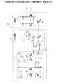
図2は、本発明の第1の実施形態に係わる増幅回路の一例を示す。第1の実施形態に係わる増幅回路100は、増幅器1およびバイアス回路2を備える。バイアス回路2は、電圧生成回路3および電流生成回路4を備える。なお、増幅回路100は、電源Vddに接続される。すなわち、電源電圧Vddが増幅器1、電圧生成回路3、電流生成回路4に印加される。<First Embodiment>
FIG. 2 shows an example of an amplifier circuit according to the first embodiment of the present invention. An
増幅器1は、負荷抵抗RL、差動トランジスタ対M1、テールトランジスタM2を備える抵抗負荷型差動増幅器である。差動トランジスタ対M1は、トランジスタM1x、M1yから構成される。トランジスタM1x、M1yの特性は、互いに実質的に同じである。各トランジスタM1x、M1yのドレインは、負荷抵抗RLを介して電源Vddに接続される。各トランジスタM1x、M1yのソースは、テールトランジスタM2のドレインに接続される。テールトランジスタM2のソースは、接地される。テールトランジスタM2のゲートは、バイアス回路2に接続される。そして、増幅器1は、差動トランジスタ対M1のゲートに与えられる入力信号を増幅する。The
電圧生成回路3は、電流源C1〜C4およびトランジスタM11〜M15を備える。トランジスタM11のドレインは、電流源C1に接続される。この例では、電流源C1により生成される電流はIbである。トランジスタM11のソースは、トランジスタM12のドレインに接続される。トランジスタM12のソースは、接地される。各トランジスタM11、M12において、ドレインとゲートとが接続されている。すなわち、各トランジスタM11、M12は、ダイオードとして動作する。The
トランジスタM13のゲートは、トランジスタM11のゲートに接続される。トランジスタM13のドレインには、電圧Vddが印加される。トランジスタM13のソースは、電流源C2を介して接地される。この例では、電流源C2により生成される電流は2Ibである。The gate of the transistor M13 is connected to the gate of the transistor M11. A voltage Vdd is applied to the drain of the transistor M13. The source of the transistor M13 is grounded through the current source C2. In this example, the current generated by the current source C2 is 2Ib.
トランジスタM14のドレインは、電流源C3に接続される。この例では、電流源C3により生成される電流はIbである。トランジスタM14のソースは、電流源C2を介して接地される。トランジスタM14において、ドレインとゲートとが接続されている。すなわち、トランジスタM14は、ダイオードとして動作する。The drain of the transistor M14 is connected to the current source C3. In this example, the current generated by the current source C3 is Ib. The source of the transistor M14 is grounded via the current source C2. In the transistor M14, the drain and the gate are connected. That is, the transistor M14 operates as a diode.
トランジスタM15のゲートは、トランジスタM14のゲートに接続される。トランジスタM15のドレインには、電圧Vddが印加される。トランジスタM15のソースは、電流源C4を介して接地される。この例では、電流源C4により生成される電流はIbである。そして、電圧生成回路3は、トランジスタM15のソースの電圧を出力する。なお、以下の記載では、電圧生成回路3の出力電圧を「参照電圧Vref」と呼ぶことがある。The gate of the transistor M15 is connected to the gate of the transistor M14. A voltage Vdd is applied to the drain of the transistor M15. The source of the transistor M15 is grounded via the current source C4. In this example, the current generated by the current source C4 is Ib. Then, the
電流生成回路4は、参照抵抗Rref、アンプ5、およびトランジスタM21を備える。アンプ5の非反転端子は、参照抵抗Rrefを介して電源Vddに接続される。アンプ5の反転端子には、電圧生成回路3により生成される参照電圧Vrefが与えられる。アンプ5の出力端子は、トランジスタM21のゲートに接続される。トランジスタM21のドレインは、アンプ5の非反転端子に接続される。トランジスタM21のソースは接地される。ここで、ノードN11の電圧は、負帰還によりVrefに保持される。そして、電流生成回路4は、参照抵抗Rrefおよび参照電圧Vrefに依存する参照電流Irefを生成する。The
トランジスタM21のゲートは、増幅器1のテールトランジスタM2のゲートに接続される。また、トランジスタM12のソースおよびテールトランジスタM2のソースは、同じ電位に接地される。よって、トランジスタM12とテールトランジスタM12のゲート・ソース間電圧は等しくなるため、テールトランジスタM2を介して流れる電流は、トランジスタM21を介して流れる電流に比例する。すなわち、参照電流Irefに比例する電流がテールトランジスタM2を介して流れる。The gate of the transistor M21 is connected to the gate of the tail transistor M2 of the
なお、図2に示す実施例では、電圧生成回路3の中に電流源C1〜C4が実装されているが、第1の実施形態はこの構成に限定されるものではない。すなわち、電流源C1〜C4は、電圧生成回路3の外に設けられてもよい。 In the example shown in FIG. 2, the current sources C1 to C4 are mounted in the
上記構成の増幅回路100において、差動トランジスタ対M1を構成するトランジスタが飽和領域で動作するものとする。そして、増幅器1の出力信号の振幅が最大となるように、増幅器1の動作点が設定される。この場合、増幅器1の出力信号の振幅を最大化する動作点Voutは、(3)式で表される。なお、Vddは、電源電圧を表す。Vth1は、差動トランジスタ対M1を構成する各トランジスタの閾値電圧を表す。Vdsat2は、テールトランジスタM2の飽和ドレイン電圧を表す。In the
ここで、図3に示すように、電流生成回路4には、電圧生成回路3により生成される参照電圧Vrefが与えられる。この場合、ノードN11の電圧は、負帰還によりVrefに保持される。そうすると、電流生成回路4により生成される参照電流Irefは、(4)式で表される。Here, as shown in FIG. 3, the reference voltage Vref generated by the
さらに、トランジスタM21とテールトランジスタM2とのサイズ比が1:nである場合、テールトランジスタM2を介して流れる電流は、n×Irefである。ここで、差動トランジスタ対M1を構成する各トランジスタM1x、M1yを介して流れる電流は、互いに同じである。よって、各負荷抵抗RLを介して流れる電流は、n×Iref/2である。したがって、動作点Voutは、(5)式で表される。Furthermore, when the size ratio of the transistor M21 and the tail transistor M2 is 1: n, the current flowing through the tail transistor M2 is n × Iref . Here, the currents flowing through the transistors M1x and M1y constituting the differential transistor pair M1 are the same. Therefore, the current flowing through each load resistor RL is n × Iref / 2. Therefore, the operating point Vout is expressed by equation (5).
ここで、(3)式と(5)式とを比較すると、増幅器1の出力信号の振幅を最大化するためには、(6)式で表される条件1および(7)式で表される条件2を満足することが要求される。 Here, when the expressions (3) and (5) are compared, in order to maximize the amplitude of the output signal of the
条件1は、参照抵抗Rrefの抵抗値、負荷抵抗RLの抵抗値、トランジスタM21とテールトランジスタM2とのサイズ比を適切に設定すれば満たされる。例えば、サイズ比nが1である場合、参照抵抗Rrefの抵抗値および負荷抵抗RLの抵抗値が互いに同じになるように、参照抵抗Rrefおよび負荷抵抗RLが形成される。あるいは、サイズ比nが2である場合には、参照抵抗Rrefの抵抗値および負荷抵抗RLの抵抗値の2倍になるように、参照抵抗Rrefおよび負荷抵抗RLが形成される。
条件2は、電圧生成回路3において、参照電圧VrefとしてVth1+Vdsat2を生成することで満たされる。すなわち、条件1を満足するように抵抗およびトランジスタを形成し、電圧生成回路3においてVth1+Vdsat2を生成すれば、増幅器1の出力信号の振幅を最大化する動作点が実現される。
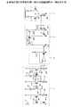
次に、図4を参照しながら、電圧生成回路3がVth1+Vdsat2を生成する動作について記載する。なお、以下の記載では、差動トランジスタ対M1を構成するトランジスタを単に「トランジスタM1」と呼ぶことがある。Next, an operation in which the
トランジスタの飽和ドレイン電圧は、そのトランジスタのサイズに依存する。具体的には、トランジスタの飽和ドレイン電圧Vdsatは、(8)式で表される。Lは、チャネル長を表す。Wは、ゲート幅を表す。μは、キャリアの実効移動度を表す。COXは、酸化膜容量を表す。The saturation drain voltage of a transistor depends on the size of the transistor. Specifically, the saturation drain voltage Vdsat of the transistor is expressed by equation (8). L represents the channel length. W represents the gate width. μ represents the effective mobility of the carrier. COX represents the oxide film capacity.
ここで、トランジスタのサイズは「W/L」で表される。よって、トランジスタのサイズを4倍にすると、飽和ドレイン電圧Vdsatは2分の1になる。また、トランジスタのサイズを4分の1にすると、飽和ドレイン電圧Vdsatは2倍になる。Here, the size of the transistor is represented by “W / L”. Therefore, when the size of the transistor is quadrupled, the saturation drain voltage Vdsat ishalved . Further, when the size of the transistor isreduced to a quarter, the saturation drain voltage Vdsat is doubled.
この例では、各トランジスタM11、M12のサイズは、図4に示すように、トランジスタM1の4倍である。たとえば、各トランジスタM11、M12のゲート幅は、トランジスタM1の4倍である。この場合、各トランジスタM11、M12の飽和ドレイン電圧は、トランジスタM1の2分の1である。よって、ノードN1の電圧V1は、(9)式で表される。Vgs11は、トランジスタM11のゲート・ソース間電圧を表す。Vgs12は、トランジスタM12のゲート・ソース間電圧を表す。Vth1は、トランジスタM1の閾値電圧を表す。Vdsat1は、トランジスタM1の飽和ドレイン電圧を表す。In this example, the size of each of the transistors M11 and M12 is four times that of the transistor M1, as shown in FIG. For example, the gate width of each of the transistors M11 and M12 is four times that of the transistor M1. In this case, the saturation drain voltage of each of the transistors M11 and M12 is half that of the transistor M1. Therefore, the voltage V1 at the node N1 is expressed by equation (9). Vgs11 represents the gate-source voltage of the transistor M11. Vgs12 represents the gate-source voltage of the transistor M12. Vth1 represents the threshold voltage of the transistor M1. Vdsat1 represents the saturation drain voltage of the transistor M1.
トランジスタM13のサイズは、トランジスタM1と同じである。ここで、ノードN2の電圧は、トランジスタM13で構成されたソースフォロアの出力電圧に相当する。したがって、ノードN2の電圧V2は、(10)式で表される。なお、Vgs13は、トランジスタM13のゲート・ソース間電圧を表す。The size of the transistor M13 is the same as that of the transistor M1. Here, the voltage at the node N2 corresponds to the output voltage of the source follower constituted by the transistor M13. Therefore, the voltage V2 at the node N2 is expressed by the equation (10). Vgs13 represents the gate-source voltage of the transistor M13.
トランジスタM14のサイズは、テールトランジスタM2の4分の1である。したがって、ノードN3の電圧V3は、(11)式で表される。なお、Vgs14は、トランジスタM14のゲート・ソース間電圧を表す。The size of the transistor M14 is a quarter of that of the tail transistor M2. Therefore, the voltage V3 at the node N3 is expressed by the equation (11). Vgs14 represents the gate-source voltage of the transistor M14.
トランジスタM15のサイズは、テールトランジスタM2と同じである。したがって、ノードN4の電圧V4は、(12)式で表される。なお、Vgs15は、トランジスタM15のゲート・ソース間電圧を表す。The size of the transistor M15 is the same as that of the tail transistor M2. Therefore, the voltage V4 at the node N4 is expressed by the equation (12). Vgs15 represents the gate-source voltage of the transistor M15.
このように、ノードN4においてVth1+Vdsat2が生成される。そして、電圧生成回路3は、ノードN4の電圧を参照電圧Vrefとして出力する。この参照電圧Vrefは、図2または図3に示すように、電流生成回路4に与えられる。そうすると、電流生成回路4は、上述した(4)式で表される参照電流Irefを生成する。In this way, Vth1 + Vdsat2 is generated at the node N4. Then, the
ここで、参照抵抗Rref、負荷抵抗RL、トランジスタM21、テールトランジスタM2は、上述した(6)式で表される条件1を満足するように形成される。よって、増幅器1は、上述した(3)式で表される最適動作点Voutで入力信号を増幅することができる。すなわち、増幅器1は、出力信号の振幅が最大化されるように入力信号を増幅できる。Here, the reference resistor Rref , the load resistor RL , the transistor M21, and the tail transistor M2 are formed so as to satisfy the
図5は、第1の実施形態による効果の一例を示す。ここでは、図1に示す回路と図2に示す第1の実施形態による回路とを比較する。横軸は電源電圧Vddを表し、縦軸は増幅器1の動作点の電圧Voutを表す。また、図1〜図2に示す回路では、増幅器1の信号範囲の上限は電源電圧Vddであり、その下限はVth1+Vdsat2がある。FIG. 5 shows an example of the effect according to the first embodiment. Here, the circuit shown in FIG. 1 is compared with the circuit according to the first embodiment shown in FIG. The horizontal axis represents the power supply voltageVdd , and the vertical axis represents the voltageVout at the operating point of the
図5に示す例では、電源電圧Vddの変化に対する増幅器1の出力動作点が表されている。ここで、増幅器1の出力信号の振幅を最大化するためには、動作点VoutがVddとVth1+Vdsat2との中点であることが要求される。ところが、図1に示す回路では、参照電圧Vrefが一定なので、電源電圧Vddが変化すると、動作点Voutは信号範囲の中点からずれてしまう。図5に示す例では、電源電圧Vddが大きい領域では、動作点Voutと上限電圧との差分に対して、動作点Voutと下限電圧との差分が大きくなっている。In the example shown in FIG. 5, the output operating point of the
これに対して、図2に示す第1の実施形態による回路では、電流生成回路4に与えられる参照電圧Vrefは、Vth1+Vdsat2に制御される。すなわち、参照電圧Vrefは、増幅器1の信号範囲の下限電圧に制御される。よって、電源電圧Vddが変化しても、増幅器1の動作点Voutは信号範囲の中点に保持される。また、図2に示す各トランジスタは、同じウエハ上に同じ工程で形成される。したがって、製造ばらつき等によって、増幅器1の信号範囲の下限電圧(すなわち、Vth1+Vdsat2)が目標レベルよりも高くなると、電圧生成回路3により生成される参照電圧Vrefも同様に目標レベルよりも高くなる。すなわち、製造ばらつき等によって回路素子の特性が変わる場合であっても、動作点Voutは信号範囲の中点に保持される。この結果、電源電圧の変動または製造ばらつきがあっても、増幅器1の出力信号の振幅が最大化される。On the other hand, in the circuit according to the first embodiment shown in FIG. 2, the reference voltage Vref given to the
<第2の実施形態>
図6は、第2の実施形態に係わる増幅回路に実装される電圧生成回路の一例を示す。なお、増幅器1および電流生成回路4は、第1の実施形態および第2の実施形態で実質的に同じである。また、図6に示す構成では、各電流源C1、C3、C5は、電流Ibを生成し、各電流源C2、C4は、電流2Ibを生成する。<Second Embodiment>
FIG. 6 shows an example of a voltage generation circuit mounted on the amplifier circuit according to the second embodiment. The
第2の実施形態では、トランジスタM11のドレインは電流源C1に接続され、そのソースは接地される。また、トランジスタM11において、ドレインとゲートとが接続される。すなわち、トランジスタM11は、ダイオードとして動作する。ここで、トランジスタM11のサイズは、増幅器1のテールトランジスタM2の4分の1である。よって、ノードN1の電圧は、Vth2+2Vdsat2である。In the second embodiment, the drain of the transistor M11 is connected to the current source C1, and its source is grounded. In the transistor M11, the drain and the gate are connected. That is, the transistor M11 operates as a diode. Here, the size of the transistor M11 is a quarter of the tail transistor M2 of the
トランジスタM12のドレインには電源電圧Vddが印加され、そのゲートはノードN1に接続される。また、トランジスタM12のソースは電流源C2を介して接地される。ここで、トランジスタM12のサイズは、テールトランジスタM2と同じである。よって、ノードN2の電圧は、Vdsat2である。A power supply voltageVdd is applied to the drain of the transistor M12, and its gate is connected to the node N1. The source of the transistor M12 is grounded via the current source C2. Here, the size of the transistor M12 is the same as that of the tail transistor M2. Therefore, the voltage at the node N2 is Vdsat2 .
トランジスタM13のドレインは電流源C3に接続され、そのソースはノードN2に接続される。また、トランジスタM13において、ドレインとゲートとが接続される。ここで、トランジスタM13のサイズは、増幅器1のトランジスタM1の4倍である。よって、ノードN3の電圧は、Vdsat2+Vth1+Vdsat1/2である。The drain of the transistor M13 is connected to the current source C3, and the source thereof is connected to the node N2. In the transistor M13, the drain and the gate are connected. Here, the size of the transistor M13 is four times that of the transistor M1 of the
トランジスタM14のドレインには電源電圧Vddが印加され、そのゲートはノードN3に接続される。また、トランジスタM14のソースは電流源C4を介して接地される。ここで、トランジスタM14のサイズは、トランジスタM1と同じである。よって、ノードN4の電圧は、Vdsat2−Vdsat1/2である。The power supply voltageVdd is applied to the drain of the transistor M14, and its gate is connected to the node N3. The source of the transistor M14 is grounded via the current source C4. Here, the size of the transistor M14 is the same as that of the transistor M1. Therefore, the voltage of the node N4 is Vdsat2 −Vdsat1 / 2.
トランジスタM15のドレインは電流源C5に接続され、そのソースはノードN4に接続される。また、トランジスタM15において、ドレインとゲートとが接続される。ここで、トランジスタM15のサイズは、増幅器1のトランジスタM1の4倍である。よって、ノードN5の電圧は、Vth1+Vdsat2である。The drain of the transistor M15 is connected to the current source C5, and the source thereof is connected to the node N4. In the transistor M15, the drain and the gate are connected. Here, the size of the transistor M15 is four times that of the transistor M1 of the
このように、ノードN5においてVth1+Vdsat2が生成される。そして、電圧生成回路3は、ノードN5の電圧を参照電圧Vrefとして出力する。すなわち、図6に示す回路によっても、第1の実施形態と同様に、増幅器1の信号範囲の下限電圧が生成される。なお、第1の実施形態と比較すると、第2の実施形態では、ソースフォロワの段数が少ない。したがって、各トランジスタに印加されるドレイン・ソース間電圧が大きくなり、電源電圧の変動に対する耐性が強くなる。Thus, Vth1 + Vdsat2 is generated at the node N5. Then, the
<第3の実施形態>
図7は、第3の実施形態に係わる増幅回路に実装される電圧生成回路の一例を示す。なお、増幅器1および電流生成回路4は、第1の実施形態および第3の実施形態で実質的に同じである。また、図7に示す構成では、各電流源C1〜C6は、電流Ibを生成する。<Third Embodiment>
FIG. 7 shows an example of a voltage generation circuit mounted on the amplifier circuit according to the third embodiment. The
第3の実施形態では、トランジスタM11のドレインは電流源C1に接続され、そのソースは電流源C2を介して接地される。トランジスタM12のドレインは電流源C3に接続され、そのソースは接地される。なお、トランジスタM11のゲートは、ノードN2を介してトランジスタM12のドレインに接続され、トランジスタM12のゲートは、ノードN1を介してトランジスタM11のソースに接続されている。ここで、トランジスタM11、M12のサイズは、それぞれ増幅器1のトランジスタM1の4倍である。よって、ノードN1の電圧はVth1+Vdsat1/2であり、ノードN2の電圧は、2Vth1+Vdsat1である。In the third embodiment, the drain of the transistor M11 is connected to the current source C1, and its source is grounded via the current source C2. The drain of the transistor M12 is connected to the current source C3, and the source thereof is grounded. Note that the gate of the transistor M11 is connected to the drain of the transistor M12 via the node N2, and the gate of the transistor M12 is connected to the source of the transistor M11 via the node N1. Here, the sizes of the transistors M11 and M12 are each four times that of the transistor M1 of the
トランジスタM13のドレインには電源電圧Vddが印加され、そのゲートはノードN2に接続される。また、トランジスタM13のソースは電流源C4を介して接地される。ここで、トランジスタM13のサイズは、トランジスタM1と同じである。よって、ノードN3の電圧は、Vth1である。A power supply voltageVdd is applied to the drain of the transistor M13, and its gate is connected to the node N2. The source of the transistor M13 is grounded via the current source C4. Here, the size of the transistor M13 is the same as that of the transistor M1. Therefore, the voltage at the node N3 is Vth1 .
図7に示す電流源C5、トランジスタM14、トランジスタM15、電流源C6は、図2に示す電流源C3、トランジスタM14、トランジスタM15、電流源C4と実質的に同じである。よって、図7において、ノードN4の電圧はVth1+Vth2+2Vdsat2であり、ノードN5の電圧は、Vth1+Vdsat2である。The current source C5, transistor M14, transistor M15, and current source C6 shown in FIG. 7 are substantially the same as the current source C3, transistor M14, transistor M15, and current source C4 shown in FIG. Therefore, in FIG. 7, the voltage at the node N4 is Vth1 + Vth2 + 2Vdsat2 , and the voltage at the node N5 is Vth1 + Vdsat2 .
このように、ノードN5においてVth1+Vdsat2が生成される。そして、電圧生成回路3は、ノードN5の電圧を参照電圧Vrefとして出力する。すなわち、図7に示す回路によっても、第1の実施形態と同様に、増幅器1の信号範囲の下限電圧が生成される。なお、第3の実施形態では、レギュレーテッドカスコードが構成される。よって、第1の実施形態と比較すると、出力抵抗が大きくなるので、電源電圧の変動に対する耐性が強くなる。Thus, Vth1 + Vdsat2 is generated at the node N5. Then, the
<第4の実施形態>
図2に示す第1の実施形態では、電流生成回路4に実装されるトランジスタM21が増幅器1のテールトランジスタM2に接続される。これに対して、第4の実施形態においては、図8に示すように、電流生成回路4と増幅器1との間のカレントミラー回路6が実装される。すなわち、電流生成回路4は、カレントミラー回路6を介して増幅器1に電気的に結合される。<Fourth Embodiment>
In the first embodiment shown in FIG. 2, the transistor M21 mounted in the
カレントミラー回路6の電流比(すなわち、カレントミラー回路6の入力電流と出力電流との比)は、特に特定の値に限定されるものではない。ただし、カレントミラー回路6の電流比は、トランジスタM21を介して流れる電流とテールトランジスタM2を介して流れる電流との比nが上述した(6)式で表される条件1を満足するように決定される。なお、カレントミラー回路6の電流比は、例えば、トランジスタM31、M32のサイズ比により決定される。 The current ratio of the current mirror circuit 6 (that is, the ratio between the input current and the output current of the current mirror circuit 6) is not particularly limited to a specific value. However, the current ratio of the current mirror circuit 6 is determined so that the ratio n of the current flowing through the transistor M21 and the current flowing through the tail transistor M2 satisfies the
この構成によれば、所望の電流を容易に生成できる。なお、図8に示す電圧生成回路3の代わりに、図6に示す電圧生成回路または図7に示す電圧生成回路が実装されるようにしてもよい。 According to this configuration, a desired current can be easily generated. Instead of the
<第5の実施形態>
図9は、本発明の第5の実施形態に係わる増幅回路の一例を示す。第5の実施形態においては、図2に示す電流源C1〜C4の代わりに、それぞれトランジスタM41〜M44が実装される。なお、図9に示すように、トランジスタM41、M43、M31のゲートは、互いに接続される。トランジスタM42、M44、M21、M33のゲートは、互いに接続される。<Fifth Embodiment>
FIG. 9 shows an example of an amplifier circuit according to the fifth embodiment of the present invention. In the fifth embodiment, transistors M41 to M44 are mounted instead of the current sources C1 to C4 shown in FIG. As shown in FIG. 9, the gates of the transistors M41, M43, and M31 are connected to each other. The gates of the transistors M42, M44, M21, and M33 are connected to each other.
上記構成において、トランジスタM42、M44には、電流生成回路4において生成される参照電流に対応する電流が流れる。また、トランジスタM41、M43は、カレントミラー回路6のトランジスタM31、M33を介して電流生成回路4に電気的に結合されている。よって、トランジスタM42、M44にも、電流生成回路4において生成される参照電流に対応する電流が流れる。すなわち、第5の実施形態においては、電流源を用いることなく、増幅回路100の中で電圧生成回路3のバイアス電流を生成できる。なお、トランジスタM41〜M44は、トランジスタM41、M42、M43、M44を介して流れる電流の比が図2に示す電流源C1、C2、C3、C4の電流比と同じになるように形成されることが好ましい。 In the above configuration, a current corresponding to the reference current generated in the
なお、図9に示す例では、第1または第4の実施形態の増幅回路内でバイアス電流が生成されるが、本発明はこの構成に限定されるものではない。すなわち、第2または第3の実施形態の増幅回路内でバイアス電流が生成されるようにしてもよい。 In the example shown in FIG. 9, the bias current is generated in the amplifier circuit of the first or fourth embodiment, but the present invention is not limited to this configuration. That is, a bias current may be generated in the amplifier circuit of the second or third embodiment.
<第6の実施形態>
図2に示す第1の実施形態では、増幅器1のテール電流源は1個のトランジスタ(すなわち、テールトランジスタM2)により実現されるが、本発明はこの構成に限定されるものではない。すなわち、増幅器1のテール電流源は、例えば、カスコード回路で実現されるようにしてもよい。<Sixth Embodiment>
In the first embodiment shown in FIG. 2, the tail current source of the
図10は、本発明の第6の実施形態に係わる増幅回路の一例を示す。図10の示す例では、増幅器1のテール電流源は、トランジスタM2、M3により構成される。トランジスタM2のドレインは、差動トランジスタ対M1に接続される。トランジスタM2のソースは、トランジスタM3のドレインに接続される。そして、トランジスタM3のソースは接地される。 FIG. 10 shows an example of an amplifier circuit according to the sixth embodiment of the present invention. In the example shown in FIG. 10, the tail current source of the
この場合、図2に示す第1の実施形態と比べると、増幅器1の信号範囲の下限電圧は、トランジスタM3の飽和ドレイン電圧の分だけ高くなる。すなわち、図10に示す構成では、増幅器1の信号範囲の下限電圧は、Vth1+Vdsat2+Vdsat3である。Vth1はトランジスタM1の閾値電圧を表す。Vdsat2およびVdsat3は、それぞれトランジスタM2およびM3の飽和ドレイン電圧を表す。In this case, compared with the first embodiment shown in FIG. 2, the lower limit voltage of the signal range of the
第6の実施形態では、増幅器1の信号範囲の下限電圧がVth1+Vdsat2+Vdsat3なので、電圧生成回路3は、Vth1+Vdsat2+Vdsat3を生成する。ここで、Vth1+Vdsat2は、図2に示す電流源C1〜C4およびトランジスタM11〜M15により生成される。すなわち、図10に示す増幅回路においても、ノードN4の電圧はVth1+Vdsat2である。そこで、第6の実施形態の電圧生成回路3は、電流源C1〜C4およびトランジスタM11〜M15に加えて、Vdsat3を生成するための回路(電流源C5〜C6およびトランジスタM16〜M17)を備える。In the sixth embodiment, since the lower limit voltage of the signal range of the
トランジスタM16のドレインは、電流源C5に接続される。電流源C5により生成される電流はIbである。トランジスタM16のソースは、ノードN4に接続される。トランジスタM16において、ドレインとゲートとが接続されている。トランジスタM17のゲートは、トランジスタM16のゲートに接続される。トランジスタM17のドレインには、電源電圧Vddが印加される。トランジスタM17のソースは、電流源C6を介して接地される。電流源C6により生成される電流はIbである。The drain of the transistor M16 is connected to the current source C5. Current generated by current source C5 is Ib. The source of the transistor M16 is connected to the node N4. In the transistor M16, the drain and the gate are connected. The gate of the transistor M17 is connected to the gate of the transistor M16. A power supply voltage Vdd is applied to the drain of the transistor M17. The source of the transistor M17 is grounded through the current source C6. Current generated by current source C6 is Ib.
ノードN4の電圧は、図4を参照しながら説明したように、Vth1+Vdsat2である。ここで、トランジスタM16のサイズは、テールトランジスタM3の4分の1である。したがって、ノードN5の電圧は、Vth1+Vdsat2+Vth3+2Vdsat3である。また、トランジスタM17のサイズは、テールトランジスタM3と同じである。したがって、ノードN6の電圧は、Vth1+Vdsat2+Vdsat3である。The voltage of the node N4 is Vth1 + Vdsat2 as described with reference to FIG. Here, the size of the transistor M16 is a quarter of that of the tail transistor M3. Therefore, the voltage of the node N5 is Vth1 + Vdsat2 + Vth3 + 2Vdsat3 . The size of the transistor M17 is the same as that of the tail transistor M3. Therefore, the voltage at the node N6 is Vth1 + Vdsat2 + Vdsat3 .
このように、ノードN6においてVth1+Vdsat2+Vdsat3が生成される。そして、電圧生成回路3は、ノードN6の電圧を参照電圧Vrefとして出力する。電流生成回路4は、参照電圧Vrefに応じて参照電流Irefを生成する。カレントミラー回路6は、トランジスタM31〜M37を備え、参照電流Irefに対応する電流を増幅器1のトランジスタM2、M3に供給する。この構成により、増幅器1のテール電流源がカスコード回路で実現される場合であっても、増幅器1の出力信号の振幅が最大化される。In this manner, Vth1 + Vdsat2 + Vdsat3 is generated at the node N6. Then, the
また、図10に示す例では、参照電圧VrefとしてVth1+Vdsat2+Vdsat3が生成される。ここで、Vth1は、差動トランジスタ対を構成するトランジスタの閾値電圧を表す。また、Vdsat2、Vdsat3は、テール電流源を構成するトランジスタM2、M3の飽和ドレイン電圧を表す。すなわち、第6の実施形態でも、電圧生成回路3は、差動トランジスタ対を構成するトランジスタの閾値電圧とテールトランジスタの飽和ドレイン電圧との和に基づいて決まる参照電圧を生成する。In the example shown in FIG. 10, Vth1 + Vdsat2 + Vdsat3 is generated as the reference voltage Vref . Here, Vth1 represents the threshold voltage of the transistors constituting the differential transistor pair. Vdsat2 and Vdsat3 represent saturation drain voltages of the transistors M2 and M3 constituting the tail current source. That is, also in the sixth embodiment, the
なお、図10に示す例では、第1または第4の実施形態をベースにして電圧生成回路3が実現されているが、本発明はこの構成に限定されるものではない。例えば、図6に示す第2の実施形態の電圧生成回路に、Vdsat3を生成する回路を追加してもよい。また、図7に示す第3の実施形態の電圧生成回路に、Vdsat3を生成する回路を追加してもよい。In the example shown in FIG. 10, the
<第7の実施形態>
図2に示す実施例では、増幅器1の差動トランジスタ対を構成するトランジスタがnチャネルトランジスタで実現されるが、本発明はこの構成に限定されるものではない。すなわち、増幅器1の差動トランジスタ対をpチャネルトランジスタで実現してもよい。<Seventh Embodiment>
In the embodiment shown in FIG. 2, the transistors constituting the differential transistor pair of the
図11は、本発明の第7の実施形態に係わる増幅回路の一例を示す図である。第7の実施形態に係わる増幅回路の構成は、図2に示す第1の実施形態と実質的に同じである。ただし、第7の実施形態では、各トランジスタはpチャネルトランジスタである。 FIG. 11 is a diagram illustrating an example of an amplifier circuit according to the seventh embodiment of the present invention. The configuration of the amplifier circuit according to the seventh embodiment is substantially the same as that of the first embodiment shown in FIG. However, in the seventh embodiment, each transistor is a p-channel transistor.
増幅器1は、負荷抵抗RL、差動トランジスタ対M1、テールトランジスタM2を備える。テールトランジスタM2のソースには、電源電圧Vddが印加される。テールトランジスタM2のドレインは、差動トランジスタ対M1の各トランジスタのソースに接続される。差動トランジスタ対M1の各トランジスタのドレインは、負荷抵抗RLを介して接地される。したがって、増幅器1の動作点Voutは、{Vdd−(Vdsat2+Vth1)}/2であることが好ましい。The
電圧生成回路3は、トランジスタM11〜M15および電流源C1〜C4を備える。トランジスタM11のソースには、電源電圧Vddが印加される。トランジスタM11のドレインは、トランジスタM12のソースに接続される。トランジスタM12のドレインは、電流源C1を介して接地される。各トランジスタM11、M12において、ソースとゲートとが接続されている。ここで、各トランジスタM11、M12のサイズは、トランジスタM1の4倍である。よって、ノードN1の電圧は、Vdd−(2Vth1+Vdsat1)である。The
トランジスタM13のソースは電流源C2に接続され、そのゲートはノードN1に接続され、そのドレインは接地される。ここで、トランジスタM13のサイズは、トランジスタM1と同じである。よって、ノードN2の電圧は、Vdd−Vth1である。The source of the transistor M13 is connected to the current source C2, its gate is connected to the node N1, and its drain is grounded. Here, the size of the transistor M13 is the same as that of the transistor M1. Therefore, the voltage of the node N2 is Vdd −Vth1 .
トランジスタM14のソースはノードN2に接続され、そのドレインは電流源C3を介した接地される。トランジスタM14において、ソースとゲートとが接続されている。ここで、トランジスタM14のサイズは、テールトランジスタM2の4分の1である。よって、ノードN3の電圧は、Vdd−Vth1−Vth2−2Vdsat2である。The source of the transistor M14 is connected to the node N2, and the drain thereof is grounded via the current source C3. In the transistor M14, the source and the gate are connected. Here, the size of the transistor M14 is a quarter of that of the tail transistor M2. Therefore, the voltage of the node N3 is Vdd −Vth1 −Vth2 −2Vdsat2 .
トランジスタM15のソースは電流源C4に接続され、そのゲートはノードN3に接続され、そのドレインは接地される。ここで、トランジスタM15のサイズは、テールトランジスタM2と同じである。よって、ノードN4の電圧は、Vdd−(Vth1+Vdsat2)である。The source of the transistor M15 is connected to the current source C4, the gate thereof is connected to the node N3, and the drain thereof is grounded. Here, the size of the transistor M15 is the same as that of the tail transistor M2. Therefore, the voltage of the node N4 is Vdd − (Vth1 + Vdsat2 ).
このように、ノードN4においてVdd−(Vth1+Vdsat2)が生成される。そして、電圧生成回路3は、ノードN4の電圧を参照電圧Vrefとして出力する。即ち、増幅器1の信号範囲の上限電圧が生成される。電流生成回路4は、参照電圧Vrefに応じて参照電流Irefを生成する。このとき、参照電流Irefは、Vref/Rrefで表される。そして、増幅器1において、この参照電流に対応するテール電流が流れる。この結果、増幅器1の動作点は、出力信号の振幅が最大化されるように制御される。なお、図11に示す構成と同様に、第2〜第6の実施形態においても、増幅器1の差動トランジスタ対をpチャネルトランジスタで構成してもよい。In this way, Vdd − (Vth1 + Vdsat2 ) is generated at the node N4. Then, the
<第8の実施形態>
図12は、第8の実施形態に係わる増幅回路に実装される電圧生成回路の一例を示す。なお、増幅器1および電流生成回路4は、第1の実施形態および第8の実施形態で実質的に同じである。<Eighth Embodiment>
FIG. 12 shows an example of a voltage generation circuit mounted on the amplifier circuit according to the eighth embodiment. The
電圧生成回路3の構成は、第1の実施形および第8の実施形態において実質的に互いに同じである。ただし、第1の実施形態では、トランジスタのサイズを適切に決めることで目的とする電圧が生成される。たとえば、トランジスタM1の飽和ドレイン電圧の2分の1の電圧を生成するために、トランジスタM1の4倍のサイズのトランジスタが形成される。あるいは、テールトランジスタM2の飽和ドレイン電圧の2倍の電圧を生成するために、テールトランジスタM2の4分の1のサイズのトランジスタが形成される。 The configuration of the
第8の実施形態では、バイアス電流を適切に決めることで目的とする電圧が生成される。ここで、トランジスタの飽和ドレイン電圧は、(13)式で表される。Lは、チャネル長を表す。Wは、ゲート幅を表す。μは、キャリアの実効移動度を表す。COXは、酸化膜容量を表す。In the eighth embodiment, the target voltage is generated by appropriately determining the bias current. Here, the saturation drain voltage of the transistor is expressed by equation (13). L represents the channel length. W represents the gate width. μ represents the effective mobility of the carrier. COX represents the oxide film capacity.
したがって、バイアス電流を4倍にすれば、飽和ドレイン電圧は2倍になる。また、バイアス電流を4分の1にすれば、飽和ドレイン電圧は2分の1になる。 Therefore, if the bias current is quadrupled, the saturation drain voltage is doubled. If the bias current is reduced to a quarter, the saturation drain voltage is reduced to a half.
図12に示す実施例では、電流源C1、C2、C3、C4により生成される電流は、それぞれIb/4、5Ib、4Ib、Ibである。トランジスタM11〜M13のサイズは、差動トランジスタ対M1を構成するトランジスタと同じである。トランジスタM14、M15のサイズは、テールトランジスタM2と同じである。In the embodiment shown in FIG. 12, the current generated by the current source C1, C2, C3, C4, respectivelyI b / 4,5I b, 4I b , a Ib. The sizes of the transistors M11 to M13 are the same as the transistors constituting the differential transistor pair M1. The size of the transistors M14 and M15 is the same as that of the tail transistor M2.
電流源C1により生成されるバイアス電流がIb/4なので、各トランジスタM11、M12の飽和ドレイン電圧は、Vdsat1の2分の1である。すなわち、各トランジスタM11、M12のゲート・ソース間電圧はVth1+Vdsat1/2である。したがって、ノードN1の電圧は2Vth1+Vdsat1であり、ノードN2の電圧はVth1である。Since the bias current generated by the current source C1 is Ib / 4, the saturation drain voltage of each of the transistors M11 and M12 is half of Vdsat1 . That is, the gate-source voltage of each of the transistors M11 and M12 is Vth1 + Vdsat1 / 2. Therefore, the voltage at the node N1 is 2Vth1 + Vdsat1 , and the voltage at the node N2 is Vth1 .
電流源C1により生成されるバイアス電流が4Ibなので、トランジスタM14の飽和ドレイン電圧は、Vdsat2の2倍である。すなわち、トランジスタM14のゲート・ソース間電圧はVth2+2Vdsat2である。よって、ノードN3の電圧はVth1+Vth2+2Vdsat2であり、ノードN4の電圧はVth1+Vdsat2である。Bias current generated by current source C1 is because 4Ib, saturation drain voltage of the transistor M14 is twiceV dsat2. That is, the gate-source voltage of the transistor M14 is Vth2 + 2Vdsat2 . Therefore, the voltage at the node N3 is Vth1 + Vth2 + 2Vdsat2 , and the voltage at the node N4 is Vth1 + Vdsat2 .
このように、図12に示す構成によっても、電圧生成回路3はVth1+Vdsat2を生成することができる。したがって、増幅器1の動作点は、出力信号の振幅が最適化されるように制御される。なお、図6に示す第2の実施形態または図7に示す第3の実施形態においても、同様に、バイアス電流を調整することでVth1+Vdsat2を生成してもよい。As described above, the
<第9の実施形態>
図13は、第9の実施形態に係わる増幅回路に実装される電圧生成回路の一例を示す。なお、増幅器1および電流生成回路4は、第1の実施形態および第9の実施形態で実質的に同じである。<Ninth Embodiment>
FIG. 13 shows an example of a voltage generation circuit mounted on the amplifier circuit according to the ninth embodiment. The
第9の実施形態の電圧生成回路3の構成は、図4に示す第1の実施形態と実質的に同じである。ただし、第1の実施形態と比較すると、第9の実施形態の各トランジスタのサイズおよびバイアス電流は、それぞれk分の1である。具体的には、電流源C1、C2、C3、C4により生成される電流は、それぞれIb/k、2Ib/k、Ib/k、Ib/kである。トランジスタM11、M12のサイズは、トランジスタM1の4/k倍である。トランジスタM13のサイズは、トランジスタM1のk分の1である。トランジスタM14のサイズは、テールトランジスタM2の4k分の1である。トランジスタM15のサイズは、テールトランジスタM2のk分の1である。なお、kは、1よりも大きい実数である。The configuration of the
ここで、トランジスタの飽和ドレイン電圧は、そのトランジスタのサイズ(チャネル長Lとゲート幅Wとの比)およびバイアス電流に依存する。具体的には、飽和ドレイン電圧Vdsatは下記(14)式で表される。Here, the saturation drain voltage of a transistor depends on the size of the transistor (the ratio between the channel length L and the gate width W) and the bias current. Specifically, the saturation drain voltage Vdsat is expressed by the following equation (14).
したがって、トランジスタのサイズおよびバイアス電流を同じ割合で変化させても、そのトランジスタの飽和ドレイン電圧は変わらない。即ち、トランジスタのサイズをk分の1に縮小し、且つ、バイアス電流をk分の1に削減しても、そのトランジスタの飽和ドレイン電圧Vdsatは変わらない。なお、「トランジスタのサイズをk分の1に縮小」は、例えば、チャネル長Lを変えることなく、ゲート幅Wをk分の1にすることで実現される。Therefore, even if the transistor size and the bias current are changed at the same rate, the saturation drain voltage of the transistor does not change. That is, even if the size of a transistor is reduced to 1 / k and the bias current is reduced to 1 / k, the saturation drain voltage Vdsat of the transistor does not change. Note that “reducing the transistor size to 1 / k” is realized, for example, by reducing the gate width W to 1 / k without changing the channel length L.
よって、図13に示す電圧生成回路3において、ノードN1の電圧は2Vth1+Vdsat1である。ノードN2の電圧はVth1である。ノードN3の電圧はVth1+Vth2+2Vdsat2である。そして、ノードN4の電圧はVth1+Vdsat2である。Therefore, in the
このように、図13に示す構成によっても、電圧生成回路3はVth1+Vdsat2を生成する。したがって、増幅器1の動作点は、出力信号の振幅が最適化されるように制御される。加えて、第9の実施形態によれば、第1の実施形態と比較して、電圧生成回路3のサイズが小さくなり、且つ、電圧生成回路3の消費電流が少なくなる。なお、図6に示す第2の実施形態または図7に示す第3の実施形態においても、同様に、各トランジスタのサイズをk分の1に縮小し、且つ、バイアス電流をk分の1に削減してもよい。Thus, the
<光モジュール>
第1〜第9の実施形態に係わる増幅回路1は、様々な用途において使用可能である。一例として、増幅回路1は、光信号を送信および受信する光モジュールにおいて使用可能である。<Optical module>
The
図14は、本発明の実施形態に係わる光モジュールの一例を示す。この光モジュール10は、図14に示すように、電気信号受信機11、光信号送信機12、光信号受信機13、電気信号送信機14を備える。電気信号受信機11、光信号送信機12、光信号受信機13、電気信号送信機14は、それぞれ第1〜第9の実施形態に係わる増幅回路100を含み、入力データ信号を増幅して差動駆動信号を生成する。 FIG. 14 shows an example of an optical module according to an embodiment of the present invention. As shown in FIG. 14, the
上記構成の光モジュール10において、例えば、光信号送信機12は、ドライバ21、光源(LD)22、光変調器23を備える。ドライバ21は、第1〜第9の実施形態に係わる増幅回路100を含み、入力データ信号を増幅して差動駆動信号を生成する。光源22は、所定の波長の連続光を生成する。光変調器23は、ドライバ21から与えられる差動駆動信号で連続光を変調して変調光信号を生成する。 In the
第1〜第9の実施形態に係わる増幅器1は、上述したように、出力信号の振幅を最大化できる。したがって、光モジュール10は、品質のよい信号を生成できる。 As described above, the
1 増幅器
2 バイアス回路
3 電圧生成回路
4 電流生成回路
6 カレントミラー回路
10 光モジュール
100 増幅回路DESCRIPTION OF
Claims (12)
Translated fromJapanese前記増幅器は、
負荷抵抗と、
前記負荷抵抗に電気的に結合する差動トランジスタ対と、
前記差動トランジスタ対に電気的に結合するテールトランジスタと、を備え、
前記バイアス回路は、
前記差動トランジスタ対を構成するトランジスタの閾値電圧と前記テールトランジスタの飽和ドレイン電圧との和に基づいて決まる参照電圧を生成する電圧生成回路と、
参照抵抗を用いて前記増幅回路の電源電圧と前記参照電圧との差分に比例する参照電流を生成する電流生成回路と、を備え、
前記電流生成回路は、前記テールトランジスタを介して流れるテール電流が前記参照電流に比例するように、前記増幅器に電気的に結合される
ことを特徴とする増幅回路。An amplifier circuit comprising an amplifier and a bias circuit for controlling the operating point of the amplifier,
The amplifier is
Load resistance,
A differential transistor pair electrically coupled to the load resistor;
A tail transistor electrically coupled to the differential transistor pair;
The bias circuit includes:
A voltage generation circuit that generates a reference voltage that is determined based on a sum of a threshold voltage of a transistor constituting the differential transistor pair and a saturation drain voltage of the tail transistor;
A current generation circuit that generates a reference current proportional to the difference between the power supply voltage of the amplifier circuit and the reference voltage using a reference resistor;
The amplifier circuit, wherein the current generation circuit is electrically coupled to the amplifier so that a tail current flowing through the tail transistor is proportional to the reference current.
2Vth1+Vdsat1を表す第1の電圧を生成する第1の回路と、
前記第1の電圧に基づいてVth1を表す第2の電圧を生成する第2の回路と、
前記第2の電圧に基づいてVth1+Vth2+2Vdast2を表す第3の電圧を生成する第3の回路と、
前記第3の電圧に基づいてVth1+Vdast2を表す前記参照電圧を生成する第4の回路と、を含み、
Vth1は、前記差動トランジスタ対を構成するトランジスタの閾値電圧を表し、
Vdsat2は、前記差動トランジスタ対を構成するトランジスタの飽和ドレイン電圧を表し、
Vth2は、前記テールトランジスタの閾値電圧を表す
Vdsat2は、前記テールトランジスタの飽和ドレイン電圧を表し、
ことを特徴とする請求項1に記載の増幅回路。The voltage generation circuit includes:
A first circuit for generating a first voltage representing 2Vth1 + Vdsat1;
A second circuit for generating a second voltage representing Vth1 based on the first voltage;
A third circuit for generating a third voltage representing Vth1 + Vth2 + 2Vdast2 based on the second voltage;
And a fourth circuit for generating the reference voltage representing Vth1 + Vdast2 based on the third voltage,
Vth1 represents the threshold voltage of the transistors constituting the differential transistor pair,
Vdsat2 represents the saturation drain voltage of the transistors constituting the differential transistor pair,
Vth2 represents the threshold voltage of the tail transistor Vdsat2 represents the saturation drain voltage of the tail transistor,
The amplifier circuit according to claim 1.
前記第1のトランジスタのサイズおよび前記第2のトランジスタのサイズは、それぞれ前記差動トランジスタ対を構成するトランジスタの4倍であり、
前記第1の回路は、前記第1の電圧として、前記第1のトランジスタのゲート・ソース間電圧および前記第2のトランジスタのゲート・ソース間電圧の和を出力する
ことを特徴とする請求項2に記載の増幅回路。The first circuit includes a first transistor and a second transistor,
The size of the first transistor and the size of the second transistor are each four times that of the transistors constituting the differential transistor pair,
The first circuit outputs a sum of a gate-source voltage of the first transistor and a gate-source voltage of the second transistor as the first voltage. An amplifier circuit according to 1.
前記第3のトランジスタのサイズは、前記差動トランジスタ対を構成するトランジスタと同じであり、
前記第2の回路は、前記第2の電圧として、前記第1の電圧と前記第3のトランジスタのゲート・ソース間電圧との差を出力する
ことを特徴とする請求項2または3に記載の増幅回路。The second circuit includes a third transistor,
The size of the third transistor is the same as the transistors constituting the differential transistor pair,
The said 2nd circuit outputs the difference of the said 1st voltage and the gate-source voltage of the said 3rd transistor as said 2nd voltage. The said 2nd circuit is characterized by the above-mentioned. Amplification circuit.
前記第4のトランジスタのサイズは、前記テールトランジスタの4分の1であり、
前記第3の回路は、前記第3の電圧として、前記第2の電圧および前記第4のトランジスタのゲート・ソース間電圧の和を出力する
ことを特徴とする請求項2〜4のいずれか1つに記載の増幅回路。The third circuit includes a fourth transistor,
The size of the fourth transistor is a quarter of the tail transistor,
The third circuit outputs the sum of the second voltage and a gate-source voltage of the fourth transistor as the third voltage. 5. An amplifier circuit described in 1.
前記第5のトランジスタのサイズは、前記テールトランジスタと同じであり、
前記第4の回路は、前記参照電圧として、前記第3の電圧と前記第5のトランジスタのゲート・ソース間電圧との差を出力する
ことを特徴とする請求項2〜5のいずれか1つに記載の増幅回路。The fourth circuit includes a fifth transistor,
The size of the fifth transistor is the same as the tail transistor;
The said 4th circuit outputs the difference of the said 3rd voltage and the gate-source voltage of the said 5th transistor as said reference voltage. Any one of Claim 2-5 characterized by the above-mentioned. An amplifier circuit according to 1.
前記差動トランジスタ対は、前記第1の負荷抵抗および前記第2の負荷抵抗にそれぞれ接続する、互いに同じ特性を有する第1の入力トランジスタおよび第2の入力トランジスタを備え、
前記テールトランジスタを介して流れるテール電流が前記参照電流のn倍であるとき、前記参照抵抗の抵抗値は前記第1の負荷抵抗の抵抗値のn倍であり、
nは、ゼロよりも大きい実数である
ことを特徴とする請求項1に記載の増幅回路。The load resistance includes a first load resistance and a second load resistance having the same resistance value,
The differential transistor pair includes a first input transistor and a second input transistor having the same characteristics and connected to the first load resistor and the second load resistor, respectively.
When the tail current flowing through the tail transistor is n times the reference current, the resistance value of the reference resistor is n times the resistance value of the first load resistor,
The amplification circuit according to claim 1, wherein n is a real number greater than zero.
前記電流生成回路は、前記カレントミラー回路を介して前記増幅器の電気的に結合される
ことを特徴とする請求項1に記載の増幅回路。A current mirror circuit for generating a current proportional to the reference current generated by the current generation circuit;
The amplifier circuit according to claim 1, wherein the current generation circuit is electrically coupled to the amplifier via the current mirror circuit.
Vth2+2Vdsat2を表す第1の電圧を生成する第1の回路と、
前記第1の電圧に基づいてVdsat2を表す第2の電圧を生成する第2の回路と、
前記第2の電圧に基づいてVdast2+Vth1+Vdsat1/2を表す第3の電圧を生成する第3の回路と、
前記第3の電圧に基づいてVdast2−Vdsat1/2を表す第4の電圧を生成する第4の回路と、
前記第4の電圧に基づいてVth1+Vdast2を表す前記参照電圧を生成する第5の回路と、を含み、
Vth1は、前記差動トランジスタ対を構成するトランジスタの閾値電圧を表し、
Vdsat2は、前記差動トランジスタ対を構成するトランジスタの飽和ドレイン電圧を表し、
Vth2は、前記テールトランジスタの閾値電圧を表す
Vdsat2は、前記テールトランジスタの飽和ドレイン電圧を表し、
ことを特徴とする請求項1に記載の増幅回路。The voltage generation circuit includes:
A first circuit for generating a first voltage representing Vth2 + 2Vdsat2,
A second circuit for generating a second voltage representing Vdsat2 based on the first voltage;
A third circuit for generating a third voltage representing Vdast2 + Vth1 + Vdsat1 / 2 based on the second voltage;
A fourth circuit for generating a fourth voltage representing Vdast2-Vdsat1 / 2 based on the third voltage;
And a fifth circuit for generating the reference voltage representing Vth1 + Vdast2 based on the fourth voltage,
Vth1 represents the threshold voltage of the transistors constituting the differential transistor pair,
Vdsat2 represents the saturation drain voltage of the transistors constituting the differential transistor pair,
Vth2 represents the threshold voltage of the tail transistor Vdsat2 represents the saturation drain voltage of the tail transistor,
The amplifier circuit according to claim 1.
Vth1+Vdsat1/2を表す第1の電圧を生成する第1の回路と、
前記第1の電圧に基づいて2Vth1+Vdsat1を表す第2の電圧を生成する第2の回路と、
前記第2の電圧に基づいてVth1を表す第3の電圧を生成する第3の回路と、
前記第3の電圧に基づいてVth1+Vth2+2Vdast2を表す第4の電圧を生成する第4の回路と、
前記第4の電圧に基づいてVth1+Vdast2を表す前記参照電圧を生成する第5の回路と、を含み、
Vth1は、前記差動トランジスタ対を構成するトランジスタの閾値電圧を表し、
Vdsat2は、前記差動トランジスタ対を構成するトランジスタの飽和ドレイン電圧を表し、
Vth2は、前記テールトランジスタの閾値電圧を表す
Vdsat2は、前記テールトランジスタの飽和ドレイン電圧を表し、
ことを特徴とする請求項1に記載の増幅回路。The voltage generation circuit includes:
A first circuit for generating a first voltage representing Vth1 + Vdsat1 / 2;
A second circuit for generating a second voltage representing 2Vth1 + Vdsat1 based on the first voltage;
A third circuit for generating a third voltage representing Vth1 based on the second voltage;
A fourth circuit for generating a fourth voltage representing Vth1 + Vth2 + 2Vdast2 based on the third voltage;
And a fifth circuit for generating the reference voltage representing Vth1 + Vdast2 based on the fourth voltage,
Vth1 represents the threshold voltage of the transistors constituting the differential transistor pair,
Vdsat2 represents the saturation drain voltage of the transistors constituting the differential transistor pair,
Vth2 represents the threshold voltage of the tail transistor Vdsat2 represents the saturation drain voltage of the tail transistor,
The amplifier circuit according to claim 1.
前記増幅器は、
負荷抵抗と、
前記負荷抵抗に電気的に結合する差動トランジスタ対と、
前記差動トランジスタ対に電気的に結合するテールトランジスタと、を備え、
前記バイアス回路は、
前記増幅回路の電源電圧と、前記差動トランジスタ対を構成するトランジスタの閾値電圧と前記テールトランジスタの飽和ドレイン電圧との和との差分に基づいて決まる参照電圧を生成する電圧生成回路と、
参照抵抗を用いて前記参照電圧に比例する参照電流を生成する電流生成回路と、を備え、
前記電流生成回路は、前記テールトランジスタを介して流れるテール電流が前記参照電流に比例するように、前記増幅器に電気的に結合される
ことを特徴とする増幅回路。An amplifier circuit comprising an amplifier and a bias circuit for controlling the operating point of the amplifier,
The amplifier is
Load resistance,
A differential transistor pair electrically coupled to the load resistor;
A tail transistor electrically coupled to the differential transistor pair;
The bias circuit includes:
A voltage generation circuit that generates a reference voltage that is determined based on a difference between a power supply voltage of the amplifier circuit and a sum of a threshold voltage of a transistor constituting the differential transistor pair and a saturation drain voltage of the tail transistor;
A current generation circuit that generates a reference current proportional to the reference voltage using a reference resistor,
The amplifier circuit, wherein the current generation circuit is electrically coupled to the amplifier so that a tail current flowing through the tail transistor is proportional to the reference current.
前記ドライバは、データ信号に基づいて前記差動駆動信号を生成する増幅器および前記増幅器の動作点を制御するバイアス回路を備え、
前記増幅器は、
負荷抵抗と、
前記負荷抵抗に電気的に結合する差動トランジスタ対と、
前記差動トランジスタ対に電気的に結合するテールトランジスタと、を備え、
前記バイアス回路は、
前記差動トランジスタ対を構成するトランジスタの閾値電圧と前記テールトランジスタの飽和ドレイン電圧との和に基づいて決まる参照電圧を生成する電圧生成回路と、
参照抵抗を用いて前記増幅回路の電源電圧と前記参照電圧との差分に比例する参照電流を生成する電流生成回路と、を備え、
前記電流生成回路は、前記テールトランジスタを介して流れるテール電流が前記参照電流に比例するように、前記増幅器に電気的に結合される
ことを特徴とする光モジュール。An optical module comprising a driver that generates a differential drive signal and an optical modulator that generates a modulated optical signal based on the differential drive signal,
The driver includes an amplifier that generates the differential drive signal based on a data signal and a bias circuit that controls an operating point of the amplifier,
The amplifier is
Load resistance,
A differential transistor pair electrically coupled to the load resistor;
A tail transistor electrically coupled to the differential transistor pair;
The bias circuit includes:
A voltage generation circuit that generates a reference voltage that is determined based on a sum of a threshold voltage of a transistor constituting the differential transistor pair and a saturation drain voltage of the tail transistor;
A current generation circuit that generates a reference current proportional to the difference between the power supply voltage of the amplifier circuit and the reference voltage using a reference resistor;
The optical module, wherein the current generation circuit is electrically coupled to the amplifier so that a tail current flowing through the tail transistor is proportional to the reference current.
Priority Applications (2)
| Application Number | Priority Date | Filing Date | Title |
|---|---|---|---|
| JP2017088533AJP2018186457A (en) | 2017-04-27 | 2017-04-27 | Amplifier circuit and optical module |
| US15/922,973US10727795B2 (en) | 2017-04-27 | 2018-03-16 | Amplifier circuit that amplifies differential signal and optical module that includes amplifier circuit |
Applications Claiming Priority (1)
| Application Number | Priority Date | Filing Date | Title |
|---|---|---|---|
| JP2017088533AJP2018186457A (en) | 2017-04-27 | 2017-04-27 | Amplifier circuit and optical module |
Publications (1)
| Publication Number | Publication Date |
|---|---|
| JP2018186457Atrue JP2018186457A (en) | 2018-11-22 |
Family
ID=63916866
Family Applications (1)
| Application Number | Title | Priority Date | Filing Date |
|---|---|---|---|
| JP2017088533APendingJP2018186457A (en) | 2017-04-27 | 2017-04-27 | Amplifier circuit and optical module |
Country Status (2)
| Country | Link |
|---|---|
| US (1) | US10727795B2 (en) |
| JP (1) | JP2018186457A (en) |
Cited By (1)
| Publication number | Priority date | Publication date | Assignee | Title |
|---|---|---|---|---|
| CN115023619A (en)* | 2020-01-14 | 2022-09-06 | 德州仪器公司 | voltage monitor |
Families Citing this family (1)
| Publication number | Priority date | Publication date | Assignee | Title |
|---|---|---|---|---|
| CN112292727B (en)* | 2018-06-27 | 2024-05-24 | 北京时代全芯存储技术股份有限公司 | Memory driving device |
Citations (9)
| Publication number | Priority date | Publication date | Assignee | Title |
|---|---|---|---|---|
| JPH05252020A (en)* | 1992-03-06 | 1993-09-28 | Fujitsu Ltd | Cmos drive circuit |
| JPH07106875A (en)* | 1993-09-30 | 1995-04-21 | Nec Corp | Semiconductor integrated circuit |
| JPH1031797A (en)* | 1996-07-16 | 1998-02-03 | Mitsubishi Precision Co Ltd | Method for specifying vehicle in parking lot, system therefor, parking charge calculation method and system therefor |
| US20080186101A1 (en)* | 2007-02-06 | 2008-08-07 | Texas Instruments Incorporated | Biasing Scheme for Low-Voltage MOS Cascode Current Mirrors |
| JP2010239481A (en)* | 2009-03-31 | 2010-10-21 | Toshiba Corp | Semiconductor integrated circuit device |
| US20120194273A1 (en)* | 2011-01-28 | 2012-08-02 | Nanya Technology Corporation | Differential receiver |
| US8803611B2 (en)* | 2012-07-30 | 2014-08-12 | Taiwan Semiconductor Manufacturing Company, Ltd. | Current mode logic circuit and method |
| JP2014164243A (en)* | 2013-02-27 | 2014-09-08 | Sumitomo Electric Ind Ltd | Light modulation module, semiconductor light modulation element |
| JP2014176040A (en)* | 2013-03-13 | 2014-09-22 | Ricoh Co Ltd | Differential output circuit, semiconductor ic for high speed serial communication, and high speed serial communication system |
Family Cites Families (3)
| Publication number | Priority date | Publication date | Assignee | Title |
|---|---|---|---|---|
| JP3383136B2 (en) | 1995-09-06 | 2003-03-04 | 旭化成マイクロシステム株式会社 | Constant amplitude clock generator |
| JP2001185964A (en) | 1999-12-22 | 2001-07-06 | Hitachi Ltd | Current mirror circuit and operational amplifier |
| JP4676885B2 (en) | 2006-01-04 | 2011-04-27 | 富士通セミコンダクター株式会社 | Bias circuit |
- 2017
- 2017-04-27JPJP2017088533Apatent/JP2018186457A/enactivePending
- 2018
- 2018-03-16USUS15/922,973patent/US10727795B2/ennot_activeExpired - Fee Related
Patent Citations (9)
| Publication number | Priority date | Publication date | Assignee | Title |
|---|---|---|---|---|
| JPH05252020A (en)* | 1992-03-06 | 1993-09-28 | Fujitsu Ltd | Cmos drive circuit |
| JPH07106875A (en)* | 1993-09-30 | 1995-04-21 | Nec Corp | Semiconductor integrated circuit |
| JPH1031797A (en)* | 1996-07-16 | 1998-02-03 | Mitsubishi Precision Co Ltd | Method for specifying vehicle in parking lot, system therefor, parking charge calculation method and system therefor |
| US20080186101A1 (en)* | 2007-02-06 | 2008-08-07 | Texas Instruments Incorporated | Biasing Scheme for Low-Voltage MOS Cascode Current Mirrors |
| JP2010239481A (en)* | 2009-03-31 | 2010-10-21 | Toshiba Corp | Semiconductor integrated circuit device |
| US20120194273A1 (en)* | 2011-01-28 | 2012-08-02 | Nanya Technology Corporation | Differential receiver |
| US8803611B2 (en)* | 2012-07-30 | 2014-08-12 | Taiwan Semiconductor Manufacturing Company, Ltd. | Current mode logic circuit and method |
| JP2014164243A (en)* | 2013-02-27 | 2014-09-08 | Sumitomo Electric Ind Ltd | Light modulation module, semiconductor light modulation element |
| JP2014176040A (en)* | 2013-03-13 | 2014-09-22 | Ricoh Co Ltd | Differential output circuit, semiconductor ic for high speed serial communication, and high speed serial communication system |
Cited By (1)
| Publication number | Priority date | Publication date | Assignee | Title |
|---|---|---|---|---|
| CN115023619A (en)* | 2020-01-14 | 2022-09-06 | 德州仪器公司 | voltage monitor |
Also Published As
| Publication number | Publication date |
|---|---|
| US10727795B2 (en) | 2020-07-28 |
| US20180316325A1 (en) | 2018-11-01 |
Similar Documents
| Publication | Publication Date | Title |
|---|---|---|
| JP4834347B2 (en) | Constant current circuit | |
| KR101451468B1 (en) | Constant current circuit and reference voltage circuit | |
| US7446607B2 (en) | Regulated cascode circuit, an amplifier including the same, and method of regulating a cascode circuit | |
| KR101911367B1 (en) | Reference current generating circuit, reference voltage generating circuit, and temperature detection circuit | |
| JP2005151460A (en) | AM intermediate frequency variable gain amplifier circuit, variable gain amplifier circuit and semiconductor integrated circuit thereof | |
| JP2018186457A (en) | Amplifier circuit and optical module | |
| US9369098B2 (en) | Inverting amplifier | |
| JP4920219B2 (en) | Operational amplifier | |
| US20150280663A1 (en) | Semiconductor circuit and amplifier circuit | |
| US10979000B2 (en) | Differential amplifier circuit | |
| CN101739056B (en) | Reference current generation circuit | |
| JP4724670B2 (en) | Semiconductor integrated circuit device | |
| JP6949463B2 (en) | Single differential conversion circuit | |
| JP2008289066A (en) | Low voltage voltage follower circuit | |
| JP4658838B2 (en) | Reference potential generator | |
| JPH10112614A (en) | Bias current supply method and circuit thereof | |
| JP2004343521A (en) | Differential amplifier | |
| JP2007318571A (en) | Operational amplifier circuit | |
| JP7025498B2 (en) | Memory control device and memory control method | |
| JP5203809B2 (en) | Current mirror circuit | |
| JP4447383B2 (en) | Push-pull amplifier | |
| JP2011250287A (en) | Operational transconductance amplifier | |
| JP2006140923A (en) | Voltage amplifier | |
| JP2005098908A (en) | Offset adjustment circuit | |
| JP2009071690A (en) | Push-pull amplifier |
Legal Events
| Date | Code | Title | Description |
|---|---|---|---|
| A521 | Request for written amendment filed | Free format text:JAPANESE INTERMEDIATE CODE: A523 Effective date:20180521 | |
| A621 | Written request for application examination | Free format text:JAPANESE INTERMEDIATE CODE: A621 Effective date:20200213 | |
| A977 | Report on retrieval | Free format text:JAPANESE INTERMEDIATE CODE: A971007 Effective date:20210125 | |
| A131 | Notification of reasons for refusal | Free format text:JAPANESE INTERMEDIATE CODE: A131 Effective date:20210202 | |
| RD03 | Notification of appointment of power of attorney | Free format text:JAPANESE INTERMEDIATE CODE: A7423 Effective date:20210331 | |
| RD04 | Notification of resignation of power of attorney | Free format text:JAPANESE INTERMEDIATE CODE: A7424 Effective date:20210331 | |
| A02 | Decision of refusal | Free format text:JAPANESE INTERMEDIATE CODE: A02 Effective date:20210803 |