JP2018185541A - Semiconductor device - Google Patents
Semiconductor deviceDownload PDFInfo
- Publication number
- JP2018185541A JP2018185541AJP2018145640AJP2018145640AJP2018185541AJP 2018185541 AJP2018185541 AJP 2018185541AJP 2018145640 AJP2018145640 AJP 2018145640AJP 2018145640 AJP2018145640 AJP 2018145640AJP 2018185541 AJP2018185541 AJP 2018185541A
- Authority
- JP
- Japan
- Prior art keywords
- film
- oxide semiconductor
- oxide
- semiconductor film
- transistor
- Prior art date
- Legal status (The legal status is an assumption and is not a legal conclusion. Google has not performed a legal analysis and makes no representation as to the accuracy of the status listed.)
- Withdrawn
Links
Images


Classifications
- H—ELECTRICITY
- H10—SEMICONDUCTOR DEVICES; ELECTRIC SOLID-STATE DEVICES NOT OTHERWISE PROVIDED FOR
- H10D—INORGANIC ELECTRIC SEMICONDUCTOR DEVICES
- H10D86/00—Integrated devices formed in or on insulating or conducting substrates, e.g. formed in silicon-on-insulator [SOI] substrates or on stainless steel or glass substrates
- H10D86/40—Integrated devices formed in or on insulating or conducting substrates, e.g. formed in silicon-on-insulator [SOI] substrates or on stainless steel or glass substrates characterised by multiple TFTs
- H10D86/421—Integrated devices formed in or on insulating or conducting substrates, e.g. formed in silicon-on-insulator [SOI] substrates or on stainless steel or glass substrates characterised by multiple TFTs having a particular composition, shape or crystalline structure of the active layer
- H10D86/423—Integrated devices formed in or on insulating or conducting substrates, e.g. formed in silicon-on-insulator [SOI] substrates or on stainless steel or glass substrates characterised by multiple TFTs having a particular composition, shape or crystalline structure of the active layer comprising semiconductor materials not belonging to the Group IV, e.g. InGaZnO
- H—ELECTRICITY
- H10—SEMICONDUCTOR DEVICES; ELECTRIC SOLID-STATE DEVICES NOT OTHERWISE PROVIDED FOR
- H10D—INORGANIC ELECTRIC SEMICONDUCTOR DEVICES
- H10D86/00—Integrated devices formed in or on insulating or conducting substrates, e.g. formed in silicon-on-insulator [SOI] substrates or on stainless steel or glass substrates
- H10D86/40—Integrated devices formed in or on insulating or conducting substrates, e.g. formed in silicon-on-insulator [SOI] substrates or on stainless steel or glass substrates characterised by multiple TFTs
- H10D86/481—Integrated devices formed in or on insulating or conducting substrates, e.g. formed in silicon-on-insulator [SOI] substrates or on stainless steel or glass substrates characterised by multiple TFTs integrated with passive devices, e.g. auxiliary capacitors
- H—ELECTRICITY
- H10—SEMICONDUCTOR DEVICES; ELECTRIC SOLID-STATE DEVICES NOT OTHERWISE PROVIDED FOR
- H10D—INORGANIC ELECTRIC SEMICONDUCTOR DEVICES
- H10D86/00—Integrated devices formed in or on insulating or conducting substrates, e.g. formed in silicon-on-insulator [SOI] substrates or on stainless steel or glass substrates
- H10D86/40—Integrated devices formed in or on insulating or conducting substrates, e.g. formed in silicon-on-insulator [SOI] substrates or on stainless steel or glass substrates characterised by multiple TFTs
- H10D86/60—Integrated devices formed in or on insulating or conducting substrates, e.g. formed in silicon-on-insulator [SOI] substrates or on stainless steel or glass substrates characterised by multiple TFTs wherein the TFTs are in active matrices
Landscapes
- Liquid Crystal (AREA)
- Thin Film Transistor (AREA)
- Devices For Indicating Variable Information By Combining Individual Elements (AREA)
- Electroluminescent Light Sources (AREA)
- Electrodes Of Semiconductors (AREA)
- Physical Vapour Deposition (AREA)
- Physical Deposition Of Substances That Are Components Of Semiconductor Devices (AREA)
Abstract
Translated fromJapaneseDescription
Translated fromJapanese本明細書などで開示する発明は表示装置、及び該表示装置を用いた電子機器に関する。 The invention disclosed in this specification and the like relates to a display device and an electronic device using the display device.
近年、液晶ディスプレイ(LCD)などのフラットパネルディスプレイが広く普及して
いる。液晶ディスプレイなどの表示装置において、行方向及び列方向に配設された画素内
には、スイッチング素子であるトランジスタと、該トランジスタと電気的に接続された液
晶素子と、該液晶素子と並列に接続された容量素子とが設けられている。In recent years, flat panel displays such as liquid crystal displays (LCDs) have become widespread. In a display device such as a liquid crystal display, in a pixel arranged in a row direction and a column direction, a transistor as a switching element, a liquid crystal element electrically connected to the transistor, and a liquid crystal element connected in parallel Capacitance elements are provided.
上記トランジスタの半導体膜を構成する半導体材料としては、アモルファス(非晶質)
シリコン又はポリ(多結晶)シリコンなどのシリコン半導体が汎用されている。As a semiconductor material constituting the semiconductor film of the above transistor, amorphous (amorphous)
Silicon semiconductors such as silicon or poly (polycrystalline) silicon are widely used.
また、半導体特性を示す金属酸化物(以下、酸化物半導体と記す。)は、トランジスタ
の半導体膜に適用できる半導体材料である。例えば、酸化亜鉛又はIn−Ga−Zn系酸
化物半導体を用いて、トランジスタを作製する技術が開示されている(特許文献1及び特
許文献2参照。)。A metal oxide exhibiting semiconductor characteristics (hereinafter referred to as an oxide semiconductor) is a semiconductor material that can be used for a semiconductor film of a transistor. For example, a technique for manufacturing a transistor using zinc oxide or an In—Ga—Zn-based oxide semiconductor is disclosed (see Patent Documents 1 and 2).
また、開口率を高めるために、トランジスタの酸化物半導体膜と同じ表面上に設けられ
た酸化物半導体膜と、トランジスタに接続する画素電極とが所定の距離を離れて設けられ
た容量素子を有する表示装置が開示されている(特許文献3参照)。In addition, in order to increase the aperture ratio, a capacitor element in which an oxide semiconductor film provided over the same surface as the oxide semiconductor film of the transistor and a pixel electrode connected to the transistor are provided at a predetermined distance is provided. A display device is disclosed (see Patent Document 3).
容量素子は一対の電極の間に誘電体膜が設けられており、一対の電極のうち、少なくと
も一方の電極は、トランジスタを構成するゲート電極、ソース又はドレインなど遮光性を
有する導電膜で形成されていること多い。A capacitor element is provided with a dielectric film between a pair of electrodes, and at least one of the pair of electrodes is formed of a light-shielding conductive film such as a gate electrode, a source, or a drain constituting a transistor. There are many things.
また、容量素子の容量値を大きくするほど、電界を加えた状況において、液晶素子の液
晶分子の配向を一定に保つことができる期間を長くすることができる。静止画を表示させ
る表示装置において、当該期間を長くできることは、画像データを書き換える回数を低減
することができ、消費電力の低減が望める。Further, as the capacitance value of the capacitor element is increased, the period during which the alignment of the liquid crystal molecules of the liquid crystal element can be kept constant can be extended in a situation where an electric field is applied. In a display device that displays a still image, being able to lengthen the period can reduce the number of times image data is rewritten and can reduce power consumption.
また、容量素子の電荷容量を大きくするためには、容量素子の占有面積を大きくする、
具体的には一対の電極が重畳している面積を大きくするという手段がある。しかしながら
、上記表示装置において、一対の電極が重畳している面積を大きくするために遮光性を有
する導電膜の面積を大きくすると、画素の開口率が低減し、画像の表示品位が低下する。In order to increase the charge capacity of the capacitive element, the area occupied by the capacitive element is increased.
Specifically, there is a means of increasing the area where a pair of electrodes overlap. However, in the display device, when the area of the conductive film having a light-shielding property is increased in order to increase the area where the pair of electrodes overlap, the aperture ratio of the pixel is reduced and the display quality of the image is deteriorated.
例えば、上記一対の電極を、透光性を有する材料で形成することによって、容量素子の
電荷容量を大きくし、且つ画素の開口率が高めることができる。しかしながら、上記透光
性を有する材料の透過率が低い場合においては、バックライト等の光源からの光量を増加
させる事になり消費電力が増加してしまうといった問題や、容量素子が着色してしまい特
定の波長の光が減衰し、画像の表示品位が低下するといった問題がある。For example, when the pair of electrodes is formed using a light-transmitting material, the charge capacity of the capacitor can be increased and the aperture ratio of the pixel can be increased. However, in the case where the transmittance of the light-transmitting material is low, the amount of light from the light source such as a backlight is increased, resulting in an increase in power consumption, and the capacitance element is colored. There is a problem that light of a specific wavelength is attenuated and the display quality of an image is lowered.
そこで、上記課題に鑑みて、本発明の一態様は、開口率が高く、且つ電荷容量を増大さ
せることが可能な容量素子を有する表示装置を提供することを課題の一つとする。また、
本発明の一態様は、画素部の透過率が高く、且つ電荷容量を増大させることが可能な容量
素子を有する表示装置を提供することを課題の一つとする。また、消費電力の低い表示装
置を提供することを課題の一つとする。In view of the above problems, an object of one embodiment of the present invention is to provide a display device including a capacitor that has a high aperture ratio and can increase charge capacity. Also,
An object of one embodiment of the present invention is to provide a display device including a capacitor in which the transmittance of the pixel portion is high and the charge capacity can be increased. Another object is to provide a display device with low power consumption.
なお、これらの課題の記載は、他の課題の存在を妨げるものではない。なお、本発明の
一態様は、これらの課題の全てを解決する必要はないものとする。なお、これら以外の課
題は、明細書、図面、請求項などの記載から、自ずと明らかとなるものであり、明細書、
図面、請求項などの記載から、これら以外の課題を抽出することが可能である。Note that the description of these problems does not disturb the existence of other problems. Note that one embodiment of the present invention does not have to solve all of these problems. Problems other than these will become apparent from the description, drawings, claims, etc., and the description,
Issues other than these can be extracted from the description of the drawings and claims.
本発明の一態様は、チャネル形成領域に第1の酸化物半導体膜を有するトランジスタと
、第1の酸化物半導体膜と同一表面上に形成される第2の酸化物半導体膜と、トランジス
タと電気的に接続される画素電極と、一対の電極間に誘電体膜が挟持された透光性を有す
る容量素子と、を有し、一対の電極の一方が第2の酸化物半導体膜であり、一対の電極の
他方が画素電極であり、第2の酸化物半導体膜の膜厚が、第1の酸化物半導体膜の膜厚よ
りも薄いことを特徴とする表示装置である。One embodiment of the present invention is a transistor including a first oxide semiconductor film in a channel formation region, a second oxide semiconductor film formed over the same surface as the first oxide semiconductor film, Connected pixel electrodes and a translucent capacitive element in which a dielectric film is sandwiched between a pair of electrodes, and one of the pair of electrodes is a second oxide semiconductor film, The display device is characterized in that the other of the pair of electrodes is a pixel electrode, and the thickness of the second oxide semiconductor film is smaller than the thickness of the first oxide semiconductor film.
透光性を有する容量素子の一対の電極の一方である第2の酸化物半導体膜の膜厚を、ト
ランジスタのチャネル形成領域に用いる第1の酸化物半導体膜の膜厚よりも薄く形成する
ことで、容量素子の透過率を向上させることができる。したがって、画素部の透過率が高
く、且つ電荷容量を増大させることが可能な容量素子を有する表示装置を提供できる。ま
た、トランジスタは、チャネル形成領域に用いる第1の酸化物半導体膜の膜厚を最適化す
ることができるので、信頼性の高い表示装置とすることができる。The thickness of the second oxide semiconductor film that is one of the pair of electrodes of the light-transmitting capacitor is formed to be smaller than the thickness of the first oxide semiconductor film used for the channel formation region of the transistor. Thus, the transmittance of the capacitor can be improved. Therefore, it is possible to provide a display device including a capacitor element in which the transmittance of the pixel portion is high and the charge capacity can be increased. In addition, since the thickness of the first oxide semiconductor film used for the channel formation region can be optimized in the transistor, a highly reliable display device can be obtained.
また、本発明の他の一態様は、チャネル形成領域に第1の酸化物半導体膜を有するトラ
ンジスタと、第1の酸化物半導体膜上に形成される第1の酸化物膜と、第1の酸化物半導
体膜と同一表面上に形成される第2の酸化物半導体膜と、第2の酸化物半導体膜上に形成
される第2の酸化物膜と、トランジスタと電気的に接続される画素電極と、一対の電極間
に誘電体膜が挟持された透光性を有する容量素子と、を有し、一対の電極の一方が第2の
酸化物半導体膜及び第2の酸化物膜であり、一対の電極の他方が画素電極であり、第2の
酸化物膜の膜厚が、第1の酸化物膜の膜厚よりも薄いことを特徴とする表示装置である。Another embodiment of the present invention is a transistor including a first oxide semiconductor film in a channel formation region, a first oxide film formed over the first oxide semiconductor film, A second oxide semiconductor film formed over the same surface as the oxide semiconductor film, a second oxide film formed over the second oxide semiconductor film, and a pixel electrically connected to the transistor An electrode and a translucent capacitive element in which a dielectric film is sandwiched between the pair of electrodes, and one of the pair of electrodes is the second oxide semiconductor film and the second oxide film The display device is characterized in that the other of the pair of electrodes is a pixel electrode, and the thickness of the second oxide film is smaller than the thickness of the first oxide film.
透光性を有する容量素子の一対の電極の一方の一部である第2の酸化物膜の膜厚を、ト
ランジスタのチャネル形成領域の一部に用いる第1の酸化物膜の膜厚よりも薄く形成する
ことで、容量素子の透過率を向上させることができる。したがって、画素部の透過率が高
く、且つ電荷容量を増大させることが可能な容量素子を有する表示装置を提供できる。The thickness of the second oxide film that is part of one of the pair of electrodes of the light-transmitting capacitor is larger than the thickness of the first oxide film used for part of the channel formation region of the transistor. By forming it thin, the transmittance of the capacitor can be improved. Therefore, it is possible to provide a display device including a capacitor element in which the transmittance of the pixel portion is high and the charge capacity can be increased.
また、本発明の他の一態様は、チャネル形成領域に第1の酸化物半導体膜を有するトラ
ンジスタと、第1の酸化物半導体膜上に形成される第1の酸化物膜と、第1の酸化物半導
体膜と同一表面上に形成される第2の酸化物半導体膜と、トランジスタと電気的に接続さ
れる画素電極と、一対の電極間に誘電体膜が挟持された透光性を有する容量素子と、を有
し、一対の電極の一方が第2の酸化物半導体膜であり、一対の電極の他方が画素電極であ
ることを特徴とする表示装置である。Another embodiment of the present invention is a transistor including a first oxide semiconductor film in a channel formation region, a first oxide film formed over the first oxide semiconductor film, A second oxide semiconductor film formed over the same surface as the oxide semiconductor film, a pixel electrode electrically connected to the transistor, and a light-transmitting property in which a dielectric film is sandwiched between a pair of electrodes The display device is characterized in that one of the pair of electrodes is a second oxide semiconductor film and the other of the pair of electrodes is a pixel electrode.
透光性を有する容量素子の一対の電極の一方は、第2の酸化物半導体膜であり、トラン
ジスタのチャネル形成領域に用いる第1の酸化物半導体膜と、第1の酸化物半導体膜上に
形成された第1の酸化物膜の積層膜と比較し単層構造で形成されている。したがって、画
素部の透過率が高く、且つ電荷容量を増大させることが可能な容量素子を有する表示装置
を提供できる。また、トランジスタは、第1の酸化物半導体膜上に第1の酸化物膜が形成
されているため、信頼性の高い表示装置とすることができる。One of the pair of electrodes of the light-transmitting capacitor element is a second oxide semiconductor film, and the first oxide semiconductor film used for a channel formation region of the transistor is formed over the first oxide semiconductor film. Compared with the laminated film of the formed first oxide film, it has a single layer structure. Therefore, it is possible to provide a display device including a capacitor element in which the transmittance of the pixel portion is high and the charge capacity can be increased. Further, since the first oxide film is formed over the first oxide semiconductor film, the transistor can be a highly reliable display device.
本発明の一態様により、開口率が高く、且つ電荷容量を増大させることが可能な容量素
子を有する表示装置を提供することができる。また、画素部の透過率が高く、且つ電荷容
量を増大させることが可能な容量素子を有する表示装置を提供することができる。また、
消費電力の低い表示装置を提供することができる。According to one embodiment of the present invention, a display device including a capacitor which has a high aperture ratio and can increase charge capacity can be provided. In addition, it is possible to provide a display device including a capacitor element in which the transmittance of the pixel portion is high and the charge capacity can be increased. Also,
A display device with low power consumption can be provided.
以下では、本発明の実施の形態について図面を用いて詳細に説明する。ただし、本発明
は以下の説明に限定されず、その形態および詳細を様々に変更し得ることは、当業者であ
れば容易に理解される。また、本発明は以下に示す実施の形態の記載内容に限定して解釈
されるものではない。Hereinafter, embodiments of the present invention will be described in detail with reference to the drawings. However, the present invention is not limited to the following description, and it will be easily understood by those skilled in the art that modes and details can be variously changed. In addition, the present invention is not construed as being limited to the description of the embodiments below.
以下に説明する本発明の構成において、同一部分又は同様の機能を有する部分には同一
の符号を異なる図面間で共通して用い、その繰り返しの説明は省略する。また、同様の機
能を有する部分を指す場合には、ハッチパターンを同じくし、特に符号を付さない場合が
ある。In the structure of the present invention described below, the same portions or portions having similar functions are denoted by the same reference numerals in different drawings, and description thereof is not repeated. In addition, when referring to a portion having a similar function, the hatch pattern may be the same, and there may be no particular reference.
本明細書で説明する各図において、各構成の大きさ、膜の厚さ、又は領域は、明瞭化の
ために誇張されている場合がある。よって、必ずしもそのスケールに限定されない。In each drawing described in this specification, the size, the film thickness, or the region of each component is exaggerated for clarity in some cases. Therefore, it is not necessarily limited to the scale.
本明細書などにおいて、第1、第2等として付される序数詞は便宜上用いるものであり
、工程順又は積層順を示すものではない。そのため、例えば、「第1の」を「第2の」又
は「第3の」などと適宜置き換えて説明することができる。また、本明細書等に記載され
ている序数詞と、本発明の一態様を特定するために用いられる序数詞は一致しない場合が
ある。In this specification and the like, the ordinal numbers attached as the first and second etc. are used for convenience and do not indicate the order of steps or the order of lamination. Therefore, for example, the description can be made by appropriately replacing “first” with “second” or “third”. In addition, the ordinal numbers described in this specification and the like may not match the ordinal numbers used to specify one embodiment of the present invention.
また、本発明の一態様における「ソース」及び「ドレイン」の機能は、回路動作におい
て電流の方向が変化する場合などには入れ替わることがある。このため、本明細書におい
ては、「ソース」及び「ドレイン」の用語は、入れ替えて用いることができるものとする
。In addition, the functions of “source” and “drain” in one embodiment of the present invention may be interchanged when the direction of current changes in circuit operation. Therefore, in this specification, the terms “source” and “drain” can be used interchangeably.
(実施の形態1)
本実施の形態では、本発明の一態様である表示装置について、図面を用いて説明する。
なお、本実施の形態では、液晶表示装置を例にして本発明の一態様である表示装置を説明
する。(Embodiment 1)
In this embodiment, a display device which is one embodiment of the present invention will be described with reference to drawings.
Note that in this embodiment, a display device which is one embodiment of the present invention is described using a liquid crystal display device as an example.
<表示装置の構成>
図1(A)に、表示装置の一例を示す。図1(A)に示す表示装置は、画素部100と
、走査線駆動回路104と、信号線駆動回路106と、各々が平行又は略平行に配設され
、且つ走査線駆動回路104によって電位が制御されるm本の走査線107と、各々が平
行又は略平行に配設され、且つ信号線駆動回路106によって電位が制御されるn本の信
号線109と、を有する。さらに、画素部100はマトリクス状に配設された複数の画素
301を有する。また、走査線107に沿って、各々が平行又は略平行に配設された容量
線115を有する。なお、容量線115は、信号線109に沿って、各々が平行又は略平
行に配設されていてもよい。また、走査線駆動回路104及び信号線駆動回路106をま
とめて駆動回路部という場合がある。なお、図1(A)において、容量線115は、走査
線駆動回路104に接続される構成について例示したが、これに限定されない。例えば、
容量線115は、走査線駆動回路104に接続されない構成としても良い。<Configuration of display device>
FIG. 1A illustrates an example of a display device. In the display device illustrated in FIG. 1A, the
The
各走査線107は、画素部100においてm行n列に配設された画素301のうち、い
ずれかの行に配設されたn個の画素301と電気的に接続される。また、各信号線109
は、m行n列に配設された画素301のうち、いずれかの列に配設されたm個の画素30
1に電気的と接続される。m、nは、ともに1以上の整数である。また、各容量線115
は、m行n列に配設された画素301のうち、いずれかの行に配設されたn個の画素30
1と電気的に接続される。なお、容量線115が、信号線109に沿って、各々が平行又
は略平行に配設されている場合は、m行n列に配設された画素301のうち、いずれかの
列に配設されたm個の画素301に電気的と接続される。Each
Is m pixels 30 arranged in any column among the
1 is electrically connected. m and n are both integers of 1 or more. In addition, each
Are the n pixels 30 arranged in any row among the
1 is electrically connected. When the
図1(B)は、図1(A)に示す表示装置が有する画素301の回路図の一例である。
図1(B)に示す画素301は、走査線107及び信号線109と電気的に接続されたト
ランジスタ103と、一方の電極がトランジスタ103のドレインと電気的に接続され、
他方の電極が一定の電位を供給する容量線115と電気的に接続された容量素子105と
、画素電極がトランジスタ103のドレイン及び容量素子105の一方の電極に電気的に
接続され、画素電極と対向して設けられる電極(対向電極)が対向電位を供給する配線に
電気的に接続された液晶素子108と、を有する。FIG. 1B is an example of a circuit diagram of the
A
The
液晶素子108は、トランジスタ103及び画素電極が形成される基板と、対向電極が
形成される基板とで挟持される液晶の光学的変調作用によって、光の透過又は非透過を制
御する素子である。または、液晶素子108は、トランジスタ103、画素電極、及び対
向電極が形成される基板と、封止用の基板とで挟持される液晶の光学的変調作用によって
、光の透過又は非透過を制御する素子である。なお、液晶の光学的変調作用は、液晶にか
かる電界(縦方向の電界又は斜め方向の電界を含む。)によって制御される。なお、画素
電極が形成される基板において対向電極(共通電極ともいう。)が形成される場合、液晶
にかかる電界は横方向の電界となる。The
なお、液晶素子108には、液晶素子だけでなく、様々な表示素子や発光素子などに適
用することも可能である。例えば、表示素子、発光素子などの一例としては、EL(エレ
クトロルミネッセンス)素子(有機物及び無機物を含むEL素子、有機EL素子、無機E
L素子)、LED(白色LED、赤色LED、緑色LED、青色LEDなど)、トランジ
スタ(電流に応じて発光するトランジスタ)、電子放出素子、液晶素子、電子インク、電
気泳動素子、グレーティングライトバルブ(GLV)、プラズマディスプレイ(PDP)
、MEMS(マイクロ・エレクトロ・メカニカル・システム)、デジタルマイクロミラー
デバイス(DMD)、DMS(デジタル・マイクロ・シャッター)、MIRASOL(登
録商標)、IMOD(インターフェアレンス・モジュレーション)素子、圧電セラミック
ディスプレイ、カーボンナノチューブ、など、電気磁気的作用により、コントラスト、輝
度、反射率、透過率などが変化する表示媒体を有するものがある。EL素子を用いた表示
装置の一例としては、ELディスプレイなどがある。電子放出素子を用いた表示装置の一
例としては、フィールドエミッションディスプレイ(FED)又はSED方式平面型ディ
スプレイ(SED:Surface−conduction Electron−emi
tter Display)などがある。液晶素子を用いた表示装置の一例としては、透
過型液晶表示装置、半透過型液晶表示装置、反射型液晶表示装置、直視型液晶表示装置、
投射型液晶表示装置などがある。電子インク又は電気泳動素子を用いた表示装置の一例と
しては、電子ペーパなどがある。Note that the
L element), LED (white LED, red LED, green LED, blue LED, etc.), transistor (transistor that emits light in response to current), electron emission element, liquid crystal element, electronic ink, electrophoretic element, grating light valve (GLV) ), Plasma display (PDP)
, MEMS (micro electro mechanical system), digital micromirror device (DMD), DMS (digital micro shutter), MIRASOL (registered trademark), IMOD (interference modulation) element, piezoelectric ceramic display, carbon Some have a display medium whose contrast, luminance, reflectance, transmittance, and the like change due to an electromagnetic action, such as a nanotube. An example of a display device using an EL element is an EL display. As an example of a display device using an electron-emitting device, a field emission display (FED) or a SED type flat display (SED: Surface-conduction Electron-emi)
tter Display). As an example of a display device using a liquid crystal element, a transmissive liquid crystal display device, a transflective liquid crystal display device, a reflective liquid crystal display device, a direct view liquid crystal display device,
There are projection type liquid crystal display devices. An example of a display device using electronic ink or an electrophoretic element is electronic paper.
次いで、液晶表示装置の画素301の具体的な例について説明する。ここでは、走査線
駆動回路104の一部の上面図を図2(A)に示し、画素301の一部の上面図を図2(
B)に示す。なお、図2(A)、(B)において、対向電極及び液晶素子は省略して図示
している。Next, a specific example of the
Shown in B). In FIGS. 2A and 2B, the counter electrode and the liquid crystal element are omitted.
図2(A)において、ゲートとして機能する導電膜304a、ゲート絶縁膜(図2(A
)に図示せず。)、チャネル形成領域が形成される酸化物半導体膜308a、ソース及び
ドレインとして機能する導電膜310a、310bによりトランジスタ102を構成する
。酸化物半導体膜308aは、ゲート絶縁膜上に設けられる。また、導電膜304aと同
時に形成された導電膜304bと、導電膜310a、310bと同時に形成された導電膜
310cと、導電膜304b及び導電膜310cを接続する透光性を有する導電膜316
aが設けられる。透光性を有する導電膜316aは、開口部374aにおいて導電膜30
4bと接続し、開口部374bにおいて導電膜310cと接続する。In FIG. 2A, a
Not shown). The
a is provided. The light-transmitting
4b and connected to the
図2(B)において、走査線107として機能する導電膜304cは、信号線109に
略直交する方向(図中左右方向)に延伸して設けられている。信号線109として機能す
る導電膜310dは、走査線107に略直交する方向(図中上下方向)に延伸して設けら
れている。容量線115として機能する導電膜310fは、信号線109と平行方向に延
伸して設けられている。なお、走査線107として機能する導電膜304cは、走査線駆
動回路104(図1(A)を参照。)と電気的に接続されており、信号線109として機
能する導電膜310d及び容量線115として機能する導電膜310fは、信号線駆動回
路106に電気的に接続されている。なお、図1(A)においては、容量線115は、走
査線駆動回路104に接続される構成について、例示したが、図2(B)に示すように、
容量線115は、信号線駆動回路106に接続されてもよい。In FIG. 2B, the
The
トランジスタ103は、走査線107及び信号線109が交差する領域に設けられてい
る。トランジスタ103は、ゲートとして機能する導電膜304c、ゲート絶縁膜(図2
(B)に図示せず。)、ゲート絶縁膜上に形成され、且つチャネル形成領域が形成される
酸化物半導体膜308b、ソース及びドレインとして機能する導電膜310d、310e
により構成される。なお、導電膜304cは、走査線としても機能し、酸化物半導体膜3
08bと重畳する領域がトランジスタ103のゲートとして機能する。また、導電膜31
0dは、信号線としても機能し、酸化物半導体膜308bと重畳する領域がトランジスタ
103のソースまたはドレインとして機能する。また、図2(B)において、走査線は、
上面形状において端部が酸化物半導体膜308bの端部より外側に位置する。このため、
走査線はバックライトなどの光源からの光を遮る遮光膜として機能する。この結果、トラ
ンジスタ103に含まれる酸化物半導体膜308bに光が照射されず、トランジスタ10
3の電気特性の変動を抑制することができる。The
Not shown in (B). ), An
Consists of. Note that the
A region overlapping with 08 b functions as the gate of the
0d also functions as a signal line, and a region overlapping with the
In the top surface shape, the end portion is located outside the end portion of the
The scanning line functions as a light shielding film that blocks light from a light source such as a backlight. As a result, the
3 can be suppressed.
また、導電膜310eは、開口部374cにおいて、画素電極として機能する透光性を
有する導電膜316bと電気的に接続されている。The
容量素子105は、開口部372において容量線115として機能する導電膜310f
と接続されている。また、容量素子105は、ゲート絶縁膜上に形成される透光性を有す
る導電膜308cと、画素電極として機能する透光性を有する導電膜316bと、トラン
ジスタ103上に設けられる窒化絶縁膜で形成される誘電体膜とで構成されている。すな
わち、容量素子105は透光性を有する。The
Connected with. The
このように容量素子105は透光性を有するため、画素301内に容量素子105を大
きく(大面積に)形成することができる。従って、開口率を高くすることが可能であり、
代表的には55%以上、好ましくは60%以上とすることが可能である。また、電荷容量
を増大させた表示装置を得ることができる。例えば、解像度の高い液晶表示装置において
は、画素の面積が小さくなり、容量素子の面積も小さくなる。このため、解像度の高い表
示装置において、容量素子に蓄積される電荷容量が小さくなる。しかしながら、本実施の
形態に示す容量素子105は透光性を有するため、当該容量素子を画素に設けることで、
各画素において十分な電荷容量を得つつ、開口率を高めることができる。代表的には、画
素密度が200ppi以上、さらには300ppi以上である高解像度の表示装置に好適
に用いることができる。Thus, since the
Typically, it can be 55% or more, preferably 60% or more. In addition, a display device with an increased charge capacity can be obtained. For example, in a high-resolution liquid crystal display device, the area of a pixel is reduced and the area of a capacitive element is also reduced. For this reason, in a display device with high resolution, the charge capacity stored in the capacitor element is reduced. However, since the
The aperture ratio can be increased while obtaining a sufficient charge capacity in each pixel. Typically, it can be suitably used for a high-resolution display device having a pixel density of 200 ppi or more, and further 300 ppi or more.
また、容量素子105の一方の電極である透光性を有する導電膜308cの膜厚は、ト
ランジスタ102、103が有する酸化物半導体膜308a、308bよりも薄い。した
がって、容量素子105の透過率を向上させることができる。The light-transmitting
また、図2(B)に示す画素301は、信号線として機能する導電膜310dと平行な
辺と比較して走査線として機能する導電膜304cと平行な辺の方が長い形状であり、且
つ容量線として機能する導電膜310fが、信号線として機能する導電膜310dと平行
な方向に延伸して設けられている。この結果、画素301に占める導電膜310fの面積
を低減することが可能であるため、開口率を高めることができる。また、容量線として機
能する導電膜310fが接続電極を用いず、直接透光性を有する導電膜308cと接する
ため、さらに開口率を高めることができる。2B has a shape in which the side parallel to the
また、本発明の一態様は、高解像度の表示装置においても、開口率を高めることができ
、且つ画素の透過率が高いため、バックライトなどの光源の光を効率よく利用することが
でき、表示装置の消費電力を低減することができる。Further, according to one embodiment of the present invention, even in a high-resolution display device, the aperture ratio can be increased and the transmittance of a pixel is high, so that light from a light source such as a backlight can be efficiently used. The power consumption of the display device can be reduced.
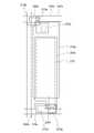
次いで、図2(A)、(B)に示す一点鎖線A−B間及び一点鎖線C−D間における断
面図を図3(A)に示す。3A is a cross-sectional view taken along the alternate long and short dash line A-B and between the alternate long and short dash line CD shown in FIGS. 2A and 2B.
図3(A)に示す本実施の形態に示す表示装置は、一対の基板(基板302と基板34
2)間に液晶素子108が挟持されている。The display device shown in this embodiment mode illustrated in FIG. 3A includes a pair of substrates (a
2) The
液晶素子108は、基板302の上方の透光性を有する導電膜316bと、配向性を制
御する膜(以下、配向膜318、352という)と、液晶層320と、導電膜350と、
を有する。なお、透光性を有する導電膜316bは、液晶素子108の一方の電極として
機能し、導電膜350は、液晶素子108の他方の電極として機能する。The
Have Note that the light-transmitting
液晶素子を有する表示装置の駆動方法としては、TNモード、STNモード、VAモー
ド、ASM(Axially Symmetric Aligned Micro−ce
ll)モード、OCB(Optically Compensated Birefri
ngence)モード、FLC(Ferroelectric Liquid Crys
tal)モード、AFLC(AntiFerroelectric Liquid Cr
ystal)モード、MVA(Multi−domain Vertical Alig
nment)モード、PVA(Patterned Vertical Alignme
nt)モード、IPSモード、FFSモード、又はTBA(Transverse Be
nd Alignment)モードなどを用いてもよい。また、液晶素子を有する表示装
置の駆動方法としては、上述した駆動方法の他、ECB(Electrically C
ontrolled Birefringence)モード、PDLC(Polymer
Dispersed Liquid Crystal)モード、PNLC(Polym
er Network Liquid Crystal)モード、ゲストホストモードな
どがある。ただし、これに限定されず、液晶素子を有する表示装置の駆動方式として様々
なものを用いることができる。As a driving method of a display device having a liquid crystal element, TN mode, STN mode, VA mode, ASM (Axial Symmetrical Aligned Micro-ce)
ll) mode, OCB (Optically Compensated Birefri)
ngence) mode, FLC (Ferroelectric Liquid Crys)
tal) mode, AFLC (Antiferroelectric Liquid Cr)
system), MVA (Multi-domain Vertical Align)
nment) mode, PVA (Patterned Vertical Alignment)
nt) mode, IPS mode, FFS mode, or TBA (Transverse Be
nd Alignment) mode or the like may be used. Further, as a driving method of a display device having a liquid crystal element, in addition to the above-described driving method, ECB (Electrically C
controlled Birefringence) mode, PDLC (Polymer)
Dispersed Liquid Crystal) mode, PNLC (Polym)
er Network Liquid Crystal) mode and guest host mode. However, the present invention is not limited to this, and various driving methods for a display device having a liquid crystal element can be used.
また、ブルー相(Blue Phase)を示す液晶とカイラル剤とを含む液晶組成物
により液晶素子を構成してもよい。ブルー相を示す液晶は、応答速度が1msec以下と
短く、光学的等方性であるため、配向処理が不要であり、視野角依存性が小さい。In addition, a liquid crystal element may be formed using a liquid crystal composition including a liquid crystal exhibiting a blue phase and a chiral agent. A liquid crystal exhibiting a blue phase has a response speed as short as 1 msec or less and is optically isotropic. Therefore, alignment treatment is unnecessary and viewing angle dependency is small.
本実施の形態においては、縦電界方式の液晶表示装置について説明する。 In this embodiment mode, a vertical electric field liquid crystal display device will be described.
このように、液晶表示装置とは、液晶素子を有する装置のことをいう。なお、液晶表示
装置は、複数の画素を駆動させる駆動回路等を含む。また、液晶表示装置は、別の基板上
に配置された制御回路、電源回路、信号生成回路及びバックライトモジュール等を含み、
液晶モジュールとよぶこともある。Thus, a liquid crystal display device refers to a device having a liquid crystal element. Note that the liquid crystal display device includes a driving circuit and the like for driving a plurality of pixels. The liquid crystal display device includes a control circuit, a power supply circuit, a signal generation circuit, a backlight module, and the like disposed on another substrate,
Sometimes called a liquid crystal module.
駆動回路部において、ゲートとして機能する導電膜304a、ゲート絶縁膜として機能
する絶縁膜305、306、チャネル形成領域が形成される酸化物半導体膜308a、ソ
ース及びドレインとして機能する導電膜310a、310bによりトランジスタ102を
構成する。酸化物半導体膜308aは、ゲート絶縁膜上に設けられる。また、酸化物半導
体膜308a、及び導電膜310a、310b上には、絶縁膜312、絶縁膜314が保
護膜として設けられている。In the driver circuit portion, a
画素部において、ゲートとして機能する導電膜304c、ゲート絶縁膜として機能する
絶縁膜305、306、ゲート絶縁膜上に形成されたチャネル形成領域が形成される酸化
物半導体膜308b、ソース及びドレインとして機能する導電膜310d、310eによ
りトランジスタ103を構成する。酸化物半導体膜308bは、ゲート絶縁膜上に設けら
れる。また、酸化物半導体膜308b、及び導電膜310d、310e上には、絶縁膜3
12、絶縁膜314が保護膜として設けられている。In the pixel portion, a
12, an insulating
また、画素部において、画素電極として機能する透光性を有する導電膜316bが、絶
縁膜312及び絶縁膜314に設けられた開口部において、導電膜310eと接続する。In the pixel portion, a light-transmitting
また、容量素子105の一方の電極として機能する透光性を有する導電膜308cと、
容量素子105の誘電体膜として機能する絶縁膜314と、容量素子105の他方の電極
として機能する透光性を有する導電膜316bと、により容量素子105を構成する。透
光性を有する導電膜308cは、ゲート絶縁膜上に設けられる。このように、透光性を有
する導電膜316bは、画素電極の機能と容量素子105の他方の電極としての機能を有
する。Further, the light-transmitting
The insulating
また、駆動回路部において、導電膜304a、304cと同時に形成された導電膜30
4bと、導電膜310a、310b、310d、310eと同時に形成された導電膜31
0cとは、透光性を有する導電膜316bと同時に形成された透光性を有する導電膜31
6aで接続される。In the driver circuit portion, the conductive film 30 formed simultaneously with the
4b and the
0c means a light-transmitting
6a is connected.
本実施の形態に示す表示装置は、トランジスタの酸化物半導体膜と同時に、容量素子の
一方となる電極を形成する。また、画素電極として機能する透光性を有する導電膜を容量
素子の他方の電極として用いる。これらのため、容量素子を形成するために、新たに導電
膜を形成する工程が不要であり、表示装置の作製工程を削減できる。また、容量素子は、
一対の電極が透光性を有する導電膜で形成されているため、透光性を有する。この結果、
容量素子の占有面積を大きくしつつ、画素の開口率を高めることができる。In the display device described in this embodiment, an electrode serving as one of the capacitor is formed at the same time as the oxide semiconductor film of the transistor. A light-transmitting conductive film functioning as a pixel electrode is used as the other electrode of the capacitor. For these reasons, a process for forming a new conductive film is not required for forming the capacitor, and the manufacturing process of the display device can be reduced. The capacitive element is
Since the pair of electrodes is formed using a light-transmitting conductive film, the electrode has a light-transmitting property. As a result,
The aperture ratio of the pixel can be increased while increasing the area occupied by the capacitor element.
また、透光性を有する導電膜308cは、酸化物半導体膜308a、308bと同時に
形成された酸化物半導体膜である。酸化物半導体膜308a、308b(酸化物半導体膜
の第1部分)は、絶縁膜306及び絶縁膜312等の、酸化物半導体膜との界面特性を向
上させることが可能な材料で形成される膜と接しているため、酸化物半導体膜308a、
308bは、半導体として機能し、酸化物半導体膜308a、308bを有するトランジ
スタは、優れた電気特性を有する。The light-transmitting
The
一方、透光性を有する導電膜308c(酸化物半導体膜の第2部分)は、開口部372
において絶縁膜314と接する。絶縁膜314は、外部からの不純物、例えば、水、アル
カリ金属、アルカリ土類金属等が、酸化物半導体膜へ拡散するのを防ぐ材料で形成される
膜であり、更には水素を含む。このため、絶縁膜314に含まれる水素が酸化物半導体膜
308a、308bと同時に形成された透光性を有する導電膜308cに拡散すると、透
光性を有する導電膜308cにおいて水素は酸素と結合し、キャリアである電子が生成さ
れる。この結果、透光性を有する導電膜308cは、導電性が高くなり導体として機能す
る。すなわち、透光性を有する導電膜308cは、導電性の高い酸化物半導体膜ともいえ
る。On the other hand, the light-transmitting
In contact with the insulating
また、透光性を有する導電膜308cは、トランジスタ102、103が有する酸化物
半導体膜308a、308bよりも膜厚が薄い。したがって、容量素子105の透過率を
向上させることができる。透光性を有する導電膜308cは、開口部372の形成時にお
いて、同時に加工することで、酸化物半導体膜308a、308bよりも膜厚を薄くする
ことが可能である。The light-transmitting
ここで、図3(A)に示す表示装置の断面図の拡大図を図3(B)に示す。図3(B)
は、図3(A)に示すトランジスタ103及び容量素子105の一部分を拡大した断面図
である。Here, an enlarged view of a cross-sectional view of the display device illustrated in FIG. 3A is illustrated in FIG. FIG. 3 (B)
FIG. 4 is an enlarged cross-sectional view of part of the
図3(B)に示すように、トランジスタ103が有する酸化物半導体膜308bの膜厚
よりも容量素子105が有する透光性を有する導電膜308cの膜厚が薄い。透光性を有
する導電膜308cの膜厚は、容量素子105の電極として機能できる導電性を有する膜
厚であり、且つ容量素子の透過率が向上できる膜厚とすると好ましい。透光性を有する導
電膜308cの膜厚としては、例えば、酸化物半導体膜308bの膜厚の2/3以下、さ
らに好ましくは1/2以下である。As shown in FIG. 3B, the thickness of the light-transmitting
次に、酸化物半導体を用いたトランジスタの特徴について記載する。酸化物半導体を用
いたトランジスタはnチャネル型トランジスタである。また、酸化物半導体に含まれる酸
素欠損はキャリアを生成する場合があり、トランジスタの電気特性及び信頼性を低下させ
る恐れがある。例えば、nチャネル型のトランジスタの場合、トランジスタのしきい値電
圧がマイナス方向に変動し、ゲート電圧が0Vの場合にドレイン電流が流れてしまうこと
がある。このように、ゲート電圧が0Vの場合にドレイン電流が流れてしまうことをノー
マリーオン特性といい、このような特性を有するトランジスタをデプレッション型トラン
ジスタという。なお、ゲート電圧が0Vの場合にドレイン電流が流れていないとみなすこ
とができるトランジスタをノーマリーオフ特性といい、このような特性を有するトランジ
スタをエンハンスメント型トランジスタという。Next, characteristics of the transistor including an oxide semiconductor are described. A transistor including an oxide semiconductor is an n-channel transistor. In addition, oxygen vacancies contained in the oxide semiconductor may generate carriers, which might reduce the electrical characteristics and reliability of the transistor. For example, in the case of an n-channel transistor, the drain voltage may flow when the threshold voltage of the transistor fluctuates in the negative direction and the gate voltage is 0V. Thus, the drain current flowing when the gate voltage is 0 V is called normally-on characteristics, and a transistor having such characteristics is called a depletion type transistor. Note that a transistor that can be regarded as having no drain current flowing when the gate voltage is 0 V is referred to as a normally-off characteristic, and a transistor having such a characteristic is referred to as an enhancement-type transistor.
トランジスタ102、103のチャネル形成領域が形成される酸化物半導体膜308a
、308bにおいて、欠陥、代表的には酸素欠損はできる限り低減されていることが好ま
しい。酸化物半導体膜に含まれる欠陥、代表的には酸素欠損をできる限り低減することで
、トランジスタ102、103がノーマリーオン特性となることを抑制することができ、
表示装置の電気特性及び信頼性を向上させることができる。また、表示装置の消費電力を
低減することができる。
308b, defects, typically oxygen vacancies, are preferably reduced as much as possible. By reducing defects contained in the oxide semiconductor film, typically oxygen vacancies as much as possible, the
The electrical characteristics and reliability of the display device can be improved. In addition, power consumption of the display device can be reduced.
トランジスタのしきい値電圧のマイナス方向への変動は酸素欠損だけではなく、酸化物
半導体に含まれる水素(水などの水素化合物を含む。)によっても引き起こされることが
ある。酸化物半導体に含まれる水素は金属原子と結合する酸素と反応して水になると共に
、酸素が脱離した格子(又は酸素が脱離した部分)に欠損(酸素欠損ともいえる。)を形
成する。また、水素の一部が酸素と反応することで、キャリアである電子を生成してしま
う。従って、水素が含まれている酸化物半導体を用いたトランジスタはノーマリーオン特
性となりやすい。Variation in the threshold voltage of the transistor in the negative direction may be caused not only by oxygen vacancies but also by hydrogen (including hydrogen compounds such as water) contained in the oxide semiconductor. Hydrogen contained in the oxide semiconductor reacts with oxygen bonded to a metal atom to become water, and also forms defects (also referred to as oxygen vacancies) in a lattice from which oxygen is released (or a portion from which oxygen is released). . In addition, a part of hydrogen reacts with oxygen to generate electrons as carriers. Therefore, a transistor including an oxide semiconductor containing hydrogen is likely to be normally on.
そこで、トランジスタ102、103のチャネル形成領域が形成される酸化物半導体膜
308a、308bにおいて、水素ができる限り低減されていることが好ましい。具体的
には、酸化物半導体膜308a、308bにおいて、二次イオン質量分析法により得られ
る水素濃度を、5×10¹⁹atoms/cm3未満、好ましくは5×1018atom
s/cm3未満、好ましくは1×1018atoms/cm3以下、より好ましくは5×
1017atoms/cm3以下、さらに好ましくは1×1016atoms/cm3以
下とする。Thus, it is preferable that hydrogen be reduced as much as possible in the
Less than s / cm3 , preferably 1 × 10¹⁸ atoms / cm3 or less, more preferably 5 ×
1017 atoms / cm3 or less, more preferably 1 × 10¹⁶ atoms / cm3 or less.
また、トランジスタ102、103のチャネル形成領域が形成される酸化物半導体膜3
08a、308bは、二次イオン質量分析法により得られるアルカリ金属又はアルカリ土
類金属の濃度を、1×10¹⁸atoms/cm3以下、好ましくは2×1016ato
ms/cm3以下にする。アルカリ金属及びアルカリ土類金属は、酸化物半導体と結合す
るとキャリアを生成する場合があり、トランジスタ102、103のオフ電流を増大させ
ることがある。In addition, the oxide semiconductor film 3 in which channel formation regions of the
For 08a and 308b, the concentration of alkali metal or alkaline earth metal obtained by secondary ion mass spectrometry is 1 × 10¹⁸ atoms / cm3 or less, preferably 2 × 10¹⁶ atoms.
Set to ms / cm3 or less. When an alkali metal and an alkaline earth metal are combined with an oxide semiconductor, carriers may be generated, and the off-state current of the
このように、酸化物半導体膜308a、308b中の不純物(水素、窒素、アルカリ金
属又はアルカリ土類金属など)をできる限り低減させ、高純度化させた酸化物半導体膜と
することで、トランジスタ102、103がエンハンスメント型となり、トランジスタ1
02、103がノーマリーオン特性となることを抑制でき、トランジスタ102、103
のオフ電流を極めて低減することができる。したがって、良好な電気特性に有する表示装
置を作製できる。また、信頼性を向上させた表示装置を作製することができる。In this manner, the
02 and 103 can be prevented from being normally on, and the
Off current can be greatly reduced. Therefore, a display device having favorable electric characteristics can be manufactured. In addition, a display device with improved reliability can be manufactured.
なお、高純度化された酸化物半導体膜を用いたトランジスタのオフ電流が低いことは、
いろいろな実験により証明できる。例えば、チャネル幅Wが1×106μmでチャネル長
Lが10μmの素子であっても、ソースとドレイン間の電圧(ドレイン電圧)が1Vから
10Vの範囲において、オフ電流が、半導体パラメータアナライザの測定限界以下、すな
わち1×10⁻¹³A以下という特性を得ることができる。この場合、オフ電流をトラン
ジスタのチャネル幅で除した値は、100zA/μm以下であることが分かる。また、容
量素子とトランジスタとを接続して、容量素子に流入又は容量素子から流出する電荷を当
該トランジスタで制御する回路を用いて、オフ電流の測定を行う。当該測定では、上記ト
ランジスタに高純度化された酸化物半導体膜をチャネル形成領域に用い、容量素子の単位
時間あたりの電荷量の推移から当該トランジスタのオフ電流を測定する。その結果、トラ
ンジスタのソースとドレイン間の電圧が3Vの場合に、数十yA/μmという、さらに低
いオフ電流が得られる。従って、高純度化された酸化物半導体膜を用いたトランジスタは
、オフ電流が著しく小さい。Note that the off-state current of a transistor including a highly purified oxide semiconductor film is low.
It can be proved by various experiments. For example, even in an element having a channel width W of 1 × 106 μm and a channel length L of 10 μm, when the voltage between the source and drain (drain voltage) is in the range of 1V to 10V, It is possible to obtain characteristics that are below the measurement limit, that is, 1 × 10⁻¹³ A or less. In this case, it can be seen that the value obtained by dividing the off-state current by the channel width of the transistor is 100 zA / μm or less. In addition, the off-state current is measured using a circuit in which a capacitor is connected to a transistor and charge that flows into or out of the capacitor is controlled by the transistor. In this measurement, a highly purified oxide semiconductor film of the transistor is used for a channel formation region, and the off-state current of the transistor is measured from the change in the amount of charge per unit time of the capacitor. As a result, when the voltage between the source and drain of the transistor is 3 V, an even lower off current of several tens of yA / μm can be obtained. Therefore, a transistor including a highly purified oxide semiconductor film has extremely small off-state current.
一方で、トランジスタ102、103が有する酸化物半導体膜308a、308bと同
一工程で形成された透光性を有する導電膜308cは、酸化物半導体膜308a、308
bと比較し、酸素欠損及び/又は水素濃度が多い。したがって、透光性を有する導電膜3
08cの導電性を高めることができる。On the other hand, the light-transmitting
Compared with b, there are more oxygen vacancies and / or hydrogen concentration. Therefore, the conductive film 3 having translucency.
The conductivity of 08c can be increased.
ここで、図3(A)に示す表示装置のその他の構成要素について、以下に説明する。 Here, other components of the display device illustrated in FIG. 3A will be described below.
基板302上には、導電膜304a、304b、304cが形成されている。導電膜3
04aは、走査線駆動回路104に形成され、駆動回路部のトランジスタのゲートとして
の機能を有する。また、導電膜304cは、画素部100に形成され、画素部のトランジ
スタのゲートとして機能する。また、導電膜304bは、走査線駆動回路104に形成さ
れ、透光性を有する導電膜316aを介して導電膜310cと接続する。On the
04a is formed in the scan
基板302としては、アルミノシリケートガラス、アルミノホウケイ酸ガラス、バリウ
ムホウケイ酸ガラスなどのガラス材料を用いる。量産する上では、基板302は、第8世
代(2160mm×2460mm)、第9世代(2400mm×2800mm、または2
450mm×3050mm)、第10世代(2950mm×3400mm)等のマザーガ
ラスを用いることが好ましい。マザーガラスは、処理温度が高く、処理時間が長いと大幅
に収縮するため、マザーガラスを使用して量産を行う場合、作製工程の加熱処理は、好ま
しくは600℃以下、さらに好ましくは450℃以下、さらに好ましくは350℃以下と
することが望ましい。As the
450 mm × 3050 mm), 10th generation (2950 mm × 3400 mm) or other mother glass is preferably used. Since the mother glass has a high processing temperature and contracts significantly when the processing time is long, when mass production is performed using the mother glass, the heat treatment in the manufacturing process is preferably 600 ° C. or less, more preferably 450 ° C. or less. Further, it is desirable that the temperature is 350 ° C. or lower.
導電膜304a、304b、304cとしては、アルミニウム、クロム、銅、タンタル
、チタン、モリブデン、タングステンから選ばれた金属元素、または上述した金属元素を
成分とする合金か、上述した金属元素を組み合わせた合金等を用いて形成することができ
る。また、導電膜304a、304b、304cは、単層構造でも、二層以上の積層構造
としてもよい。例えば、アルミニウム膜上にチタン膜を積層する二層構造、窒化チタン膜
上にチタン膜を積層する二層構造、窒化チタン膜上にタングステン膜を積層する二層構造
、窒化タンタル膜または窒化タングステン膜上にタングステン膜を積層する二層構造、チ
タン膜と、そのチタン膜上にアルミニウム膜を積層し、さらにその上にチタン膜を形成す
る三層構造等がある。また、アルミニウムに、チタン、タンタル、タングステン、モリブ
デン、クロム、ネオジム、スカンジウムから選ばれた元素の膜、または複数組み合わせた
合金膜、もしくは窒化膜を用いてもよい。As the
基板302、及び導電膜304a、304b、304c上には、絶縁膜305、306
が形成されている。絶縁膜305、306は、走査線駆動回路104のトランジスタ10
2のゲート絶縁膜、及び画素部100のトランジスタ103のゲート絶縁膜としての機能
を有する。The insulating
Is formed. The insulating
2 gate insulating films and the gate insulating film of the
絶縁膜305は、外部からの不純物、例えば、水、アルカリ金属、アルカリ土類金属等
が、酸化物半導体膜へ拡散するのを防ぐ材料を用いることが好ましく、更には水素を含む
ことが好ましい。絶縁膜305は、代表的には窒化絶縁膜である。該窒化絶縁膜としては
、例えば、窒化シリコン膜、窒化酸化シリコン膜、窒化アルミニウム膜、窒化酸化アルミ
ニウム膜などを用いればよく、積層または単層で設ける。また、絶縁膜305を積層構造
とした場合、第1の窒化シリコン膜として、欠陥が少ない窒化シリコン膜とし、第1の窒
化シリコン膜上に、第2の窒化シリコン膜として、水素放出量の少ない窒化シリコン膜を
設けると好適である。この結果、絶縁膜305に含まれる水素及び窒素が、酸化物半導体
膜308a、308bへ移動または拡散することを抑制できる。The insulating
なお、酸化窒化シリコンとは、酸素の含有量が窒素の含有量より大きな絶縁材料のこと
をいう。また、窒化酸化シリコンとは、窒素の含有量が酸素の含有量より大きい絶縁材料
のことをいう。Note that silicon oxynitride refers to an insulating material in which the oxygen content is higher than the nitrogen content. Silicon nitride oxide refers to an insulating material in which the nitrogen content is higher than the oxygen content.
絶縁膜306は、酸化物半導体膜308a、308bとの界面特性を向上させることが
可能な材料を用いることが好ましく、代表的には、酸素を含む無機絶縁材料を用いること
が好ましい。絶縁膜306は、代表的には酸化絶縁膜である。該酸化絶縁膜としては、例
えば、酸化シリコン膜、酸化窒化シリコン膜、酸化アルミニウム膜、酸化窒化アルミニウ
ム膜などを用いればよく、積層または単層で設ける。The insulating
また、絶縁膜306として、ハフニウムシリケート(HfSiOx)、窒素を有するハ
フニウムシリケート(HfSixOyNz)、窒素を有するハフニウムアルミネート(H
fAlxOyNz)、酸化ハフニウム、酸化イットリウムなどのhigh−k材料を用い
ることでトランジスタ102、103のゲートリークを低減できる。Further, as the insulating
fAlx Oy Nz), hafnium oxide, can reduce gate leakage current of the
窒化シリコン膜は、酸化シリコン膜と比較して比誘電率が高く、酸化シリコン膜と同等
の静電容量を得るのに必要な膜厚が大きいため、ゲート絶縁膜を物理的に厚膜化すること
ができる。よって、トランジスタの絶縁耐圧の低下を抑制、さらには絶縁耐圧を向上させ
て、トランジスタの静電破壊を抑制することができる。Since the silicon nitride film has a higher relative dielectric constant than the silicon oxide film and has a large film thickness necessary to obtain the same capacitance as the silicon oxide film, the gate insulating film is physically thickened. be able to. Therefore, a decrease in the withstand voltage of the transistor can be suppressed, and further, the withstand voltage can be improved to suppress electrostatic breakdown of the transistor.
また、絶縁膜306上には、酸化物半導体膜308a、308b、透光性を有する導電
膜308cが形成されている。酸化物半導体膜308aは、導電膜304aと重畳する位
置に形成され、駆動回路部のトランジスタ102のチャネル形成領域として機能する。ま
た、酸化物半導体膜308bは、導電膜304cと重畳する位置に形成され、画素部10
0のトランジスタ103のチャネル形成領域として機能する。透光性を有する導電膜30
8cは、容量素子105の一方の電極として機能する。Over the insulating
It functions as a channel formation region of the zero
8 c functions as one electrode of the
酸化物半導体膜308a、308bは、In若しくはGaを含む酸化物半導体膜であり
、代表的には、In−Ga酸化物、In−Zn酸化物、In−M−Zn酸化物(MはAl
、Ti、Ga、Y、Zr、La、Ce、Nd、またはHf)がある。The
, Ti, Ga, Y, Zr, La, Ce, Nd, or Hf).
なお、酸化物半導体膜308a、308bがIn−M−Zn酸化物であるとき、Inと
Mの原子の比率は、好ましくは、Inが50atomic%未満、Mが50atomic
%以上、さらに好ましくは、Inが25atomic%未満、Mが75atomic%以
上とする。Note that in the case where the
%, More preferably, In is less than 25 atomic% and M is 75 atomic% or more.
酸化物半導体膜308a、308bに含まれる材料の含有量(例えば、InやGaなど
)は、飛行時間型二次イオン質量分析法(TOF−SIMS)や、X線電子分光法(XP
S)で比較できる。The content of materials contained in the
S) can be compared.
酸化物半導体膜308a、308bは、エネルギーギャップが2eV以上、好ましくは
2.5eV以上、より好ましくは3eV以上であるため、後に形成されるトランジスタの
オフ電流を低減することができる。Since the energy gap of the
透光性を有する導電膜308cは、酸化物半導体膜308a、308bと同様に、In
若しくはGaを含む酸化物半導体膜であり、且つ不純物が含まれていることを特徴とする
。不純物としては、水素がある。なお、水素の代わりに不純物として、ホウ素、リン、ス
ズ、アンチモン、希ガス元素、アルカリ金属、アルカリ土類金属等が含まれていてもよい
。The light-transmitting
Alternatively, the oxide semiconductor film contains Ga and contains impurities. An impurity is hydrogen. Note that boron, phosphorus, tin, antimony, a rare gas element, an alkali metal, an alkaline earth metal, or the like may be contained as an impurity instead of hydrogen.
酸化物半導体膜308a、308b、及び透光性を有する導電膜308cは共に、ゲー
ト絶縁膜上に形成され、In若しくはGaを含む酸化物半導体膜であるが、不純物濃度が
異なる。具体的には、酸化物半導体膜308a、308bと比較して、透光性を有する導
電膜308cの不純物濃度が高い。例えば、酸化物半導体膜308a、308bに含まれ
る水素濃度は、5×10¹⁹atoms/cm3未満、好ましくは5×1018atom
s/cm3未満、好ましくは1×1018atoms/cm3以下、より好ましくは5×
1017atoms/cm3以下、さらに好ましくは1×1016atoms/cm3以
下であり、透光性を有する導電膜308cに含まれる水素濃度は、8×10¹⁹atom
s/cm3以上、好ましくは1×1020atoms/cm3以上、より好ましくは5×
1020atoms/cm3以上である。また、酸化物半導体膜308a、308bと比
較して、透光性を有する導電膜308cに含まれる水素濃度は2倍、好ましくは10倍以
上である。The
Less than s / cm3 , preferably 1 × 10¹⁸ atoms / cm3 or less, more preferably 5 ×
1017 atoms / cm3 or lower, more preferably 1 × 10¹⁶ atoms / cm3 or lower, and the hydrogen concentration contained in the light-transmitting
s / cm3 or more, preferably 1 × 10²⁰ atoms / cm3 or more, more preferably 5 ×
1020 atoms / cm3 or more. Further, the concentration of hydrogen contained in the light-transmitting
また、透光性を有する導電膜308cは、酸化物半導体膜308a、308bより抵抗
率が低い。透光性を有する導電膜308cの抵抗率が、酸化物半導体膜308a、308
bの抵抗率の1×10⁻⁸倍以上1×10⁻¹倍以下で有ることが好ましく、代表的には
1×10⁻³Ωcm以上1×10⁴Ωcm未満、さらに好ましくは、抵抗率が1×10−
3Ωcm以上1×10⁻¹Ωcm未満であるとよい。The light-transmitting
The resistivity of b is preferably 1 × 10⁻⁸ times or more and 1 × 10⁻¹ times or less, typically 1 × 10⁻³ Ωcm or more and less than 1 × 10⁴ Ωcm, more preferably the resistivity is 1 × 10−
It is good that it is3 Ωcm or more and less than 1 × 10⁻¹ Ωcm.
酸化物半導体膜308a、308b、及び透光性を有する導電膜308cは、例えば非
単結晶構造でもよい。非単結晶構造は、例えば、後述するCAAC−OS(C Axis
Aligned Crystalline Oxide Semiconductor
)、多結晶構造、後述する微結晶構造、または非晶質構造を含む。The
Aligned Crystalline Oxide Semiconductor
), A polycrystalline structure, a microcrystalline structure described later, or an amorphous structure.
なお、酸化物半導体膜308a、308b、及び透光性を有する導電膜308cが、C
AAC−OS、微結晶構造、及び非晶質構造の二以上の構造の領域を有する混合膜であっ
てもよい。混合膜は、例えば、非晶質構造の領域と、微結晶構造の領域と、CAAC−O
Sの領域と、を有する。また、混合膜は、例えば、非晶質構造の領域と、微結晶構造の領
域と、CAAC−OSの領域と、の積層構造を有してもよい。Note that the
A mixed film including a region having two or more structures of an AAC-OS, a microcrystalline structure, and an amorphous structure may be used. The mixed film includes, for example, an amorphous structure region, a microcrystalline structure region, a CAAC-O,
S region. The mixed film may have a stacked structure of an amorphous structure region, a microcrystalline structure region, and a CAAC-OS region, for example.
なお、酸化物半導体膜は、例えば、単結晶を有してもよい。 Note that the oxide semiconductor film may include a single crystal, for example.
絶縁膜306、酸化物半導体膜308a、308b、及び透光性を有する導電膜308
c上には、導電膜(以下、導電膜310a、310b、310c、310d、310eと
いう)が形成されている。また、導電膜310aは、酸化物半導体膜308aと電気的に
接続され、駆動回路部のトランジスタ102が有するソース及びドレインの一方としての
機能を有する。また、導電膜310bは、酸化物半導体膜308aと電気的に接続され、
駆動回路部のトランジスタ102が有するソース及びドレインの他方としての機能を有す
る。また、導電膜310cは、絶縁膜312、絶縁膜314に設けられた開口部を介して
、透光性を有する導電膜316aと電気的に接続されている。また、導電膜310dは、
酸化物半導体膜308bと電気的に接続され、画素部のトランジスタ103が有するソー
ス及びドレインの一方としての機能を有する。また、導電膜310eは、酸化物半導体膜
308b及び透光性を有する導電膜316bと電気的に接続され、画素部のトランジスタ
103が有するソース及びドレインの他方としての機能を有する。The insulating
A conductive film (hereinafter referred to as
The
It is electrically connected to the
導電膜310a、310b、310c、310d、310eとしては、導電材料として
、アルミニウム、チタン、クロム、ニッケル、銅、イットリウム、ジルコニウム、モリブ
デン、銀、タンタル、またはタングステンからなる単体金属、またはこれを主成分とする
合金を単層構造または積層構造として用いる。例えば、アルミニウム膜上にチタン膜を積
層する二層構造、タングステン膜上にチタン膜を積層する二層構造、銅−マグネシウム−
アルミニウム合金膜上に銅膜を積層する二層構造、チタン膜または窒化チタン膜と、その
チタン膜または窒化チタン膜上に重ねてアルミニウム膜または銅膜を積層し、さらにその
上にチタン膜または窒化チタン膜を形成する三層構造、モリブデン膜または窒化モリブデ
ン膜と、そのモリブデン膜または窒化モリブデン膜上に重ねてアルミニウム膜または銅膜
を積層し、さらにその上にモリブデン膜または窒化モリブデン膜を形成する三層構造等が
ある。なお、酸化インジウム、酸化錫または酸化亜鉛を含む透明導電材料を用いてもよい
。As the
A two-layer structure in which a copper film is laminated on an aluminum alloy film, a titanium film or a titanium nitride film, an aluminum film or a copper film laminated on the titanium film or the titanium nitride film, and a titanium film or a nitridation thereon A three-layer structure for forming a titanium film, a molybdenum film or a molybdenum nitride film, and an aluminum film or a copper film stacked on the molybdenum film or the molybdenum nitride film, and a molybdenum film or a molybdenum nitride film is further formed thereon. There are three-layer structures. Note that a transparent conductive material containing indium oxide, tin oxide, or zinc oxide may be used.
絶縁膜306、酸化物半導体膜308a、308b、透光性を有する導電膜308c、
及び導電膜310a、310b、310c、310d、310e上には、絶縁膜312、
絶縁膜314が形成されている。絶縁膜312は、絶縁膜306と同様に、酸化物半導体
膜との界面特性を向上させることが可能な材料を用いることが好ましい。絶縁膜314は
、絶縁膜305と同様に、外部からの不純物、例えば、水、アルカリ金属、アルカリ土類
金属等が、酸化物半導体膜308a、308bへ拡散するのを防ぐ材料を用いることが好
ましい。An insulating
And the insulating
An insulating
また、絶縁膜312は、化学量論的組成を満たす酸素よりも多くの酸素を含む酸化絶縁
膜で形成してもよい。このようにすることで、酸化物半導体膜308a、308bからの
酸素の脱離を防止するとともに、絶縁膜312に含まれる酸素を酸化物半導体膜に移動さ
せ、酸素欠損を補填することが可能となる。例えば、昇温脱離ガス分析(以下、TDS分
析とする。)によって測定される、100℃以上700℃以下、好ましくは100℃以上
500℃以下の加熱処理における酸素分子の放出量が、1.0×10¹⁸分子/cm3以
上ある酸化絶縁膜を用いることで、酸化物半導体膜308a、308bに含まれる酸素欠
損を補填することができる。The insulating
また、絶縁膜312を積層構造とし、酸化物半導体膜308a、308bに接する側に
第1の酸化絶縁膜として、酸化物半導体膜308a、308bとの界面準位が低くなる酸
化絶縁膜を設け、その上に第2の酸化絶縁膜として上記化学量論的組成を満たす酸素より
も多くの酸素を含む酸化絶縁膜を設けてもよい。In addition, the insulating
例えば、第1の酸化絶縁膜として、電子スピン共鳴測定によるg値=2.001(E´
−center)のスピン密度が3.0×10¹⁷spins/cm3以下、好ましくは
5.0×10¹⁶spins/cm3以下の酸化絶縁膜を用いることで、酸化物半導体膜
308a、308bとの界面準位を低減することが可能である。なお、電子スピン共鳴測
定によるg値=2.001のスピン密度は、第1の酸化絶縁膜に含まれるダングリングボ
ンドの存在量に対応する。For example, as the first oxide insulating film, g value = 2.001 (E ′ by electron spin resonance measurement)
-Center) with an oxide insulating film having a spin density of 3.0 × 10¹⁷ spins / cm3 or less, preferably 5.0 × 10¹⁶ spins / cm3 or less, so that the
また、絶縁膜314上には透光性を有する導電膜316a、316bが形成されている
。透光性を有する導電膜316aは、開口部374aにおいて導電膜304bと電気的に
接続され、開口部374bにおいて導電膜310cと電気的に接続される。すなわち、透
光性を有する導電膜316aは、導電膜304b及び導電膜310cを接続する接続電極
として機能する。また、透光性を有する導電膜316bは、開口部374cにおいて導電
膜310eと電気的に接続され、画素の画素電極としての機能を有する。また、透光性を
有する導電膜316bは、容量素子105の一対の電極の他方として機能することができ
る。In addition, light-transmitting
透光性を有する導電膜316a、316bは、酸化インジウム、酸化スズ、及び酸化亜
鉛の群から選択された少なくとも一つの酸化物を含む。透光性を有する導電膜316a、
316bとしては、例えば、酸化タングステンを含むインジウム酸化物、酸化タングステ
ンを含むインジウム亜鉛酸化物、酸化チタンを含むインジウム酸化物、酸化チタンを含む
インジウム錫酸化物、ITO、インジウム亜鉛酸化物、酸化ケイ素を添加したインジウム
錫酸化物などの透光性を有する導電性材料を用いることができる。The light-transmitting
Examples of 316b include indium oxide including tungsten oxide, indium zinc oxide including tungsten oxide, indium oxide including titanium oxide, indium tin oxide including titanium oxide, ITO, indium zinc oxide, and silicon oxide. A light-transmitting conductive material such as added indium tin oxide can be used.
また、基板342の下方には、有色性を有する膜(以下、有色膜346という。)が形
成されている。有色膜346は、カラーフィルタとしての機能を有する。また、有色膜3
46に隣接する遮光膜344が基板342の下方に形成される。遮光膜344は、ブラッ
クマトリクスとして機能する。また、有色膜346は、必ずしも設ける必要はなく、例え
ば、表示装置が白黒の場合等によって、有色膜346を設けない構成としてもよい。A colored film (hereinafter referred to as a colored film 346) is formed below the
A
有色膜346としては、特定の波長帯域の光を透過する有色膜であればよく、例えば、
赤色の波長帯域の光を透過する赤色(R)のカラーフィルタ、緑色の波長帯域の光を透過
する緑色(G)のカラーフィルタ、青色の波長帯域の光を透過する青色(B)のカラーフ
ィルタなどを用いることができる。The
A red (R) color filter that transmits light in the red wavelength band, a green (G) color filter that transmits light in the green wavelength band, and a blue (B) color filter that transmits light in the blue wavelength band Etc. can be used.
遮光膜344としては、特定の波長帯域の光を遮光する機能を有していればよく、金属
膜または黒色顔料等を含んだ有機絶縁膜などを用いることができる。As the light-blocking
また、有色膜346の下方には、絶縁膜348が形成されている。絶縁膜348は、平
坦化層としての機能、または有色膜346が含有しうる不純物を液晶素子側へ拡散するの
を抑制する機能を有する。An insulating
また、絶縁膜348上には、導電膜350が形成されている。導電膜350は、画素部
の液晶素子108が有する一対の電極の1つとしての機能を有する。なお、透光性を有す
る導電膜316a、316b、及び導電膜350に接して、配向膜318、352が形成
されている。A
また、透光性を有する導電膜316bと導電膜350との間、より具体的には配向膜3
18と配向膜352の間には、液晶層320が形成されている。また液晶層320は、シ
ール材(図示しない)を用いて、基板302と基板342の間に封止されている。なお、
シール材は、外部からの水分等の入り込みを抑制するために、無機材料と接触する構成が
好ましい。Further, between the
A
In order to suppress the entry of moisture or the like from the outside, the sealing material is preferably configured to come into contact with an inorganic material.
また、透光性を有する導電膜316a、316bと導電膜350との間に液晶層320
の厚さ(セルギャップともいう)を維持するスペーサを設けてもよい。Further, the
A spacer for maintaining the thickness (also referred to as a cell gap) may be provided.
<表示装置の作製方法>
次に、図3(A)に示す表示装置の基板302上に設けられた素子部の作製方法につい
て、図4乃至図7を用いて説明する。<Method for Manufacturing Display Device>
Next, a method for manufacturing the element portion provided over the
まず、基板302を準備する。ここでは、基板302としてガラス基板を用いる。 First, the
次に、基板302上に導電膜を形成し、該導電膜を所望の形状に加工することで、導電
膜304a、304b、304cを形成する。なお、導電膜304a、304b、304
cの形成は、所望の領域に第1のパターニングによるマスクの形成を行い、該マスクに覆
われていない領域をエッチングすることで形成することができる。(図4(A)参照)。Next, a conductive film is formed over the
The formation of c can be performed by forming a mask by first patterning in a desired region and etching a region not covered by the mask. (See FIG. 4A).
また、導電膜304a、304b、304cは、代表的には、蒸着法、CVD法、スパ
ッタリング法、スピンコート法等を用いて形成することができる。ここでは、導電膜30
4a、304b、304cとして、厚さ100nmのタングステン膜をスパッタリング法
により形成する。The
As 4a, 304b, and 304c, a tungsten film having a thickness of 100 nm is formed by a sputtering method.
次に、基板302、及び導電膜304a、304b、304c上に、絶縁膜305を形
成し、絶縁膜305上に絶縁膜306を形成する(図4(A)参照)。Next, the insulating
絶縁膜305及び絶縁膜306は、スパッタリング法、CVD法等により形成すること
ができる。なお、絶縁膜305及び絶縁膜306は、真空中で連続して形成すると絶縁膜
305と絶縁膜306との界面に不純物の混入が抑制され好ましい。ここでは、絶縁膜3
05として、厚さ400nmの窒化シリコン膜をPE−CVD法により形成する。また、
絶縁膜306として、厚さ50nmの酸化窒化シリコン膜をPE−CVD法により形成す
る。The insulating
As 05, a silicon nitride film having a thickness of 400 nm is formed by PE-CVD. Also,
As the insulating
次に、絶縁膜306上に酸化物半導体膜307を形成する(図4(B)参照)。 Next, the
酸化物半導体膜307は、スパッタリング法、塗布法、パルスレーザー蒸着法、レーザ
ーアブレーション法などを用いて形成することができる。The
スパッタリング法で酸化物半導体膜307を形成する場合、プラズマを発生させるため
の電源装置は、RF電源装置、AC電源装置、DC電源装置等を適宜用いることができる
。In the case where the
スパッタリングガスは、希ガス(代表的にはアルゴン)、酸素、希ガス及び酸素の混合
ガスを適宜用いる。なお、希ガス及び酸素の混合ガスの場合、希ガスに対して酸素のガス
比を高めることが好ましい。As the sputtering gas, a rare gas (typically argon), oxygen, a rare gas, and a mixed gas of oxygen are used as appropriate. Note that in the case of a mixed gas of a rare gas and oxygen, it is preferable to increase the gas ratio of oxygen to the rare gas.
なお、酸化物半導体膜307を形成する際に、例えば、スパッタリング法を用いる場合
、基板温度を室温(例えば20℃)以上500℃未満、好ましくは基板温度を100℃以
上450℃以下、さらに好ましくは150℃以上350℃以下として、加熱しながら酸化
物半導体膜307を形成してもよい。Note that when the
なお、スパッタリング法により酸化物半導体膜307を形成する場合、酸化物半導体膜
307の水素濃度を低減するために、スパッタリング装置における各チャンバーを、酸化
物半導体膜にとって不純物となる水素等を可能な限り除去することが可能なクライオポン
プのような吸着式の真空排気ポンプを用いて高真空排気(5×10⁻⁷Pa〜1×10−
4Pa程度まで)することが好ましい。または、ターボ分子ポンプとコールドトラップを
組み合わせて排気系からチャンバー内に気体、特に炭素または水素を含む気体が逆流しな
いようにしておくことが好ましい。Note that in the case where the
Preferably up to about4 Pa). Alternatively, it is preferable to combine a turbo molecular pump and a cold trap so that a gas, particularly a gas containing carbon or hydrogen, does not flow backward from the exhaust system into the chamber.
また、酸化物半導体膜307の水素濃度を低減するために、チャンバー内を高真空排気
するのみならずスパッタリングガスの高純度化も必要である。スパッタリングガスとして
用いる酸素ガスやアルゴンガスは、露点が−40℃以下、好ましくは−80℃以下、より
好ましくは−100℃以下、より好ましくは−120℃以下にまで高純度化したガスを用
いることで酸化物半導体膜に水分等が取り込まれることを可能な限り防ぐことができる。In addition, in order to reduce the hydrogen concentration of the
ここでは、酸化物半導体膜307として厚さ35〜100nmのIn−Ga−Zn酸化
物膜(In:Ga:Zn=1:1:1)をスパッタリング法により形成する。Here, an In—Ga—Zn oxide film (In: Ga: Zn = 1: 1: 1) with a thickness of 35 to 100 nm is formed as the
次に、酸化物半導体膜307を所望の形状に加工することで、島状の酸化物半導体膜3
08a、308b、308dを形成する(図4(C)参照)。Next, the
08a, 308b, and 308d are formed (see FIG. 4C).
なお、酸化物半導体膜308a、308b、308dの形成は、所望の領域に第2のパ
ターニングによるマスクの形成を行い、該マスクに覆われていない領域をエッチングする
ことで形成することができる。エッチングとしては、ドライエッチング、ウエットエッチ
ング、または双方を組み合わせたエッチングを用いることができる。Note that the
次に、第1の加熱処理を行うこがと好ましい。第1の加熱処理は、250℃以上650
℃以下、好ましくは300℃以上500℃以下の温度で、不活性ガス雰囲気、酸化性ガス
を10ppm以上含む雰囲気、または減圧状態で行えばよい。また、第1の加熱処理の雰
囲気は、不活性ガス雰囲気で加熱処理した後に、脱離した酸素を補うために酸化性ガスを
10ppm以上含む雰囲気で行ってもよい。第1の加熱処理によって、酸化物半導体膜3
08a、308b、308dに用いる酸化物半導体の結晶性を高め、さらに絶縁膜306
、及び酸化物半導体膜308a、308b、308dから水素や水などの不純物を除去す
ることができる。なお、酸化物半導体をエッチングする前に第1の加熱工程を行ってもよ
い。Next, it is preferable to perform the first heat treatment. The first heat treatment is performed at 250 ° C. or higher and 650 ° C.
The reaction may be performed at a temperature of not higher than ° C., preferably not lower than 300 ° C. and not higher than 500 ° C., in an inert gas atmosphere, an atmosphere containing an oxidizing gas of 10 ppm or higher, or under reduced pressure. The atmosphere of the first heat treatment may be performed in an atmosphere containing 10 ppm or more of an oxidizing gas in order to supplement desorbed oxygen after heat treatment in an inert gas atmosphere. By the first heat treatment, the oxide semiconductor film 3
The crystallinity of the oxide semiconductor used for 08a, 308b, and 308d is increased, and the insulating
In addition, impurities such as hydrogen and water can be removed from the
ここでは、350℃の窒素雰囲気で1時間加熱処理した後、350℃の酸素雰囲気で1
時間加熱処理する。Here, after heat treatment in a nitrogen atmosphere at 350 ° C. for 1 hour, 1 ° C. in an oxygen atmosphere at 350 ° C.
Heat treatment for hours.
次に、絶縁膜306、及び酸化物半導体膜308a、308b、308d上に導電膜3
09を形成する(図5(A)参照)。Next, the conductive film 3 is formed over the insulating
09 is formed (see FIG. 5A).
導電膜309としては、例えば、スパッタリング法を用いて形成することができる。 For example, the
ここでは、厚さ50nmのチタン膜、厚さ400nmのアルミニウム膜、及び厚さ10
0nmのチタン膜を順にスパッタリング法により積層する。Here, a titanium film with a thickness of 50 nm, an aluminum film with a thickness of 400 nm, and a thickness of 10
A titanium film with a thickness of 0 nm is sequentially laminated by a sputtering method.
次に、導電膜309を所望の領域に加工することで、導電膜310a、310b、31
0c、310d、310eを形成する。なお、導電膜310a、310b、310c、3
10d、310eの形成は、所望の領域に第3のパターニングによるマスクの形成を行い
、該マスクに覆われていない領域をエッチングすることで形成することができる(図5(
B)参照)。Next, the
0c, 310d, and 310e are formed. The
10d and 310e can be formed by forming a mask by third patterning in a desired region and etching a region not covered with the mask (FIG. 5 (
B)).
次に、絶縁膜306、酸化物半導体膜308a、308b、308d、及び導電膜31
0a、310b、310c、310d、310e上を覆うように、絶縁膜311を形成す
る(図5(C)参照)。Next, the insulating
An insulating
絶縁膜311としては、酸化物半導体膜308a、308b、308dとの界面特性を
向上させることが可能な材料を用いることが好ましく、代表的には、酸素を含む無機絶縁
材料を用いることが好ましく、例えば酸化絶縁膜を用いることができる。また、絶縁膜3
11としては、例えば、PE−CVD法、スパッタリング法等を用いて形成することがで
きる。As the insulating
11 can be formed using, for example, a PE-CVD method, a sputtering method, or the like.
なお、絶縁膜311として、化学量論的組成を満たす酸素よりも多くの酸素を含む酸化
絶縁膜で形成する場合、絶縁膜311は以下の形成条件を用いて形成できる。なお、ここ
では絶縁膜311として、酸化シリコン膜又は酸化窒化シリコン膜を形成する場合につい
て記載する。当該形成条件は、PE−CVD装置の真空排気された処理室内に載置された
基板を180℃以上260℃以下、さらに好ましくは180℃以上230℃以下に保持し
、処理室に原料ガスを導入して処理室内における圧力を100Pa以上250Pa以下、
さらに好ましくは100Pa以上200Pa以下とし、処理室内に設けられた電極に0.
17W/cm2以上0.5W/cm2以下、さらに好ましくは0.25W/cm2以上0
.35W/cm2以下の高周波電力を供給する、ことである。Note that in the case where the insulating
More preferably, the pressure is 100 Pa or more and 200 Pa or less.
17 W / cm2 or more and 0.5 W / cm2 or less, more preferably 0.25 W / cm2 or more and 0
. Supplying high frequency power of 35 W / cm2 or less.
絶縁膜311の原料ガスは、シリコンを含む堆積性気体の代表例としては、シラン、ジ
シラン、トリシラン、フッ化シランなどがある。酸化性気体としては、酸素、オゾン、一
酸化二窒素、二酸化窒素などがある。As a source gas for the insulating
絶縁膜311の形成条件として、上記圧力の処理室において上記パワー密度の高周波電
力を供給することで、プラズマ中で原料ガスの分解効率が高まり、酸素ラジカルが増加し
、原料ガスの酸化が進むため、絶縁膜311中における酸素含有量が化学量論的組成より
も多くなる。しかしながら、基板温度が、上記温度であると、シリコンと酸素の結合力が
弱いため、加熱により酸素の一部が脱離する。この結果、化学量論的組成を満たす酸素よ
りも多くの酸素を含み、加熱により酸素の一部が脱離する酸化絶縁膜を形成することがで
きる。As the conditions for forming the insulating
また、絶縁膜311を積層構造とし、第1の酸化絶縁膜として、少なくとも酸化物半導
体膜308a、308bとの界面準位が低くなる酸化絶縁膜を設け、その上に第2の酸化
絶縁膜として上記化学量論的組成を満たす酸素よりも多くの酸素を含む酸化絶縁膜を設け
てもよい。In addition, the insulating
少なくとも酸化物半導体膜308a、308bとの界面準位が低くなる酸化絶縁膜は、
以下の形成条件を用いて形成できる。なお、ここでは当該酸化絶縁膜として、酸化シリコ
ン膜又は酸化窒化シリコン膜を形成する場合について記載する。当該形成条件は、PE−
CVD装置の真空排気された処理室内に載置された基板を180℃以上400℃以下、さ
らに好ましくは200℃以上370℃以下に保持し、処理室に原料ガスのシリコンを含む
堆積性気体及び酸化性気体を導入して処理室内における圧力を20Pa以上250Pa以
下、さらに好ましくは40Pa以上200Pa以下とし、処理室内に設けられた電極に高
周波電力を供給する条件である。An oxide insulating film whose interface state with at least the
It can be formed using the following formation conditions. Note that the case where a silicon oxide film or a silicon oxynitride film is formed as the oxide insulating film is described here. The formation conditions are PE-
The substrate placed in the evacuated processing chamber of the CVD apparatus is held at 180 ° C. or higher and 400 ° C. or lower, more preferably 200 ° C. or higher and 370 ° C. or lower. The conditions are such that a high pressure power is supplied to the electrode provided in the processing chamber by introducing a reactive gas to a pressure in the processing chamber of 20 Pa to 250 Pa, more preferably 40 Pa to 200 Pa.
第1の酸化絶縁膜の原料ガスは、化学量論的組成を満たす酸素よりも多くの酸素を含む
酸化絶縁膜に適用できる原料ガスとすることができる。なお、第1の酸化絶縁膜は、第2
の酸化絶縁膜の形成工程において、少なくとも酸化物半導体膜308a、308bの保護
膜となる。この結果、パワー密度の高い高周波電力を用いて第2の酸化絶縁膜を形成して
も、酸化物半導体膜308a、308bへのダメージを抑制できる。The source gas for the first oxide insulating film can be a source gas that can be used for an oxide insulating film containing more oxygen than the stoichiometric composition. Note that the first oxide insulating film is the second oxide film.
In the step of forming the oxide insulating film, at least the protective film for the
ここでは、絶縁膜311を第1の酸化絶縁膜及び第2の酸化絶縁膜の積層構造とし、第
1の酸化絶縁膜として、流量30sccmのシラン及び流量4000sccmの一酸化二
窒素を原料ガスとし、処理室の圧力を200Pa、基板温度を220℃とし、27.12
MHzの高周波電源を用いて150Wの高周波電力を平行平板電極に供給したPE−CV
D装置により、厚さ50nmの酸化窒化シリコン膜を形成する。第2の酸化絶縁膜として
、流量200sccmのシラン及び流量4000sccmの一酸化二窒素を原料ガスとし
、処理室の圧力を200Pa、基板温度を220℃とし、27.12MHzの高周波電源
を用いて1500Wの高周波電力を平行平板電極に供給したPE−CVD装置により、厚
さ400nmの酸化窒化シリコン膜を形成する。なお、PE−CVD装置は電極面積が6
000cm2である平行平板型のPE−CVD装置であり、供給した電力を単位面積あた
りの電力(電力密度)に換算すると0.26W/cm2である。Here, the insulating
PE-CV which supplied 150W high frequency power to parallel plate electrodes using a high frequency power supply of MHz
A silicon oxynitride film having a thickness of 50 nm is formed by the D apparatus. As the second oxide insulating film, silane with a flow rate of 200 sccm and dinitrogen monoxide with a flow rate of 4000 sccm are used as source gas, the pressure of the processing chamber is 200 Pa, the substrate temperature is 220 ° C., and a high-frequency power source of 27.12 MHz is used for 1500 W. A 400-nm-thick silicon oxynitride film is formed by a PE-CVD apparatus that supplies high-frequency power to parallel plate electrodes. The PE-CVD apparatus has an electrode area of 6
A PE-CVD apparatus of a parallel plate type is 000cm2, a 0.26 W / cm2 when converted to electric power supplied to the power per unit area (power density).
次に、絶縁膜311を所望の形状に加工することで、絶縁膜312、及び開口部372
を形成する。なお、開口部372の形成は、所望の領域に第4のパターニングによるマス
クの形成を行い、該マスクに覆われていない領域をエッチングすることで形成することが
できる。(図6(A)参照)。Next, the insulating
Form. Note that the
なお、開口部372は、酸化物半導体膜308dが露出するように形成する。また、開
口部372の形成によって、酸化物半導体膜308d(酸化物半導体膜307の第2部分
)
は、酸化物半導体膜308a、308b(酸化物半導体膜307の第1部分)よりも膜厚
が薄くなる。具体的には、酸化物半導体膜308dの膜厚は、酸化物半導体膜308a、
308bの膜厚の2/3以下、さらに好ましくは1/2以下である。なお、酸化物半導体
膜308dの膜厚の下限は、のちに形成される透光性を有する導電膜308cが容量素子
の一方の電極として機能できる範囲であればよく、例えば5nm以上50nm以下とする
ことができる。酸化物半導体膜308dの膜厚を上記範囲とすることで、酸化物半導体膜
308dの透過率を酸化物半導体膜308a及び308bと比べ向上させることができる
。本実施の形態においては、酸化物半導体膜307として厚さ35〜100nmを形成す
るため、酸化物半導体膜308dの膜厚としては、例えば、15nm以上50nm以下と
することができる。Note that the
Is thinner than the
It is 2/3 or less of the film thickness of 308b, more preferably 1/2 or less. Note that the lower limit of the thickness of the
開口部372の形成方法としては、例えば、ドライエッチング法を用いることができる
。ただし、開口部372の形成方法としては、これに限定されず、ウエットエッチング法
、またはドライエッチング法とウエットエッチング法を組み合わせた形成方法としてもよ
い。As a method for forming the
また、本実施の形態においては、酸化物半導体膜308dの外周が絶縁膜312によっ
て覆われるように開口部372を形成したが、これに限定されない。例えば、開口部37
2の形成時において、酸化物半導体膜308dの全面を露出させ、酸化物半導体膜308
dの全面の膜厚を薄膜化してもよい。In this embodiment, the
2, the entire surface of the
The film thickness of the entire surface of d may be reduced.
次に、絶縁膜312、及び酸化物半導体膜308d上に絶縁膜313を形成する。絶縁
膜313を形成することによって、酸化物半導体膜308dは、透光性を有する導電膜3
08cとなる(図6(B)参照)。Next, the insulating
08c (see FIG. 6B).
絶縁膜313は、外部からの不純物、例えば、水、アルカリ金属、アルカリ土類金属等
が、酸化物半導体膜へ拡散するのを防ぐ材料で形成される膜であり、更には水素を含む。
このため、絶縁膜313の水素が酸化物半導体膜308dに拡散すると、該酸化物半導体
膜308dにおいて水素は酸素と結合し、キャリアである電子が生成される。この結果、
酸化物半導体膜308dは、導電性が高くなり、透光性を有する導電膜308cとなる。
一方、酸化物半導体膜308a、308bは、絶縁膜313との間に絶縁膜312を有す
るため、絶縁膜313に含まれる水素の拡散がない、または極めて少ない。絶縁膜313
には、例えば窒化シリコン膜を用いることができる。絶縁膜313は、例えば、PE−C
VD法を用いて形成することができる。The insulating
Therefore, when hydrogen in the insulating
The
On the other hand, the
For example, a silicon nitride film can be used. The insulating
It can be formed using the VD method.
上記窒化シリコン膜は、ブロック性を高めるために、高温で成膜されることが好ましく
、例えば基板温度100℃以上基板の歪み点以下、より好ましくは300℃以上400℃
以下の温度で加熱して成膜することが好ましい。また高温で成膜する場合は、酸化物半導
体膜308a、308bとして用いる酸化物半導体から酸素が脱離し、キャリア濃度が上
昇する現象が発生することがあるため、このような現象が発生しない温度とする。The silicon nitride film is preferably formed at a high temperature in order to improve blocking properties. For example, the substrate temperature is 100 ° C. or higher and the substrate strain point or lower, more preferably 300 ° C. or higher and 400 ° C.
It is preferable to form a film by heating at the following temperature. In the case where the film is formed at a high temperature, oxygen may be desorbed from the oxide semiconductors used as the
ここでは、絶縁膜313として、流量50sccmのシランと、流量5000sccm
の窒素と、流量100sccmのアンモニアとを原料ガスとし、処理室の圧力を200P
a、基板温度を220℃とし、27.12MHzの高周波電源を用いて1000W(電力
密度としては1.6×10⁻¹W/cm2)の高周波電力を平行平板電極に供給したPE
−CVD法により、厚さ50nmの窒化シリコン膜を形成する。Here, as the insulating
Nitrogen and ammonia at a flow rate of 100 sccm are used as source gases, and the pressure in the processing chamber is 200 P.
a, PE with a substrate temperature of 220 ° C. and a high frequency power of 1000 W (power density is 1.6 × 10⁻¹ W / cm2 ) supplied to parallel plate electrodes using a high frequency power supply of 27.12 MHz
A silicon nitride film having a thickness of 50 nm is formed by a CVD method.
次に、絶縁膜313を所望の形状に加工することで、絶縁膜314、及び開口部374
a、374b、374cを形成する。なお、絶縁膜314、及び開口部374a、374
b、374cは、所望の領域に第5のパターニングによるマスクの形成を行い、該マスク
に覆われていない領域をエッチングすることで形成することができる(図6(C)参照)
。Next, the insulating
a, 374b and 374c are formed. Note that the insulating
b and 374c can be formed by forming a mask by a fifth patterning in a desired region and etching a region not covered with the mask (see FIG. 6C).
.
また、開口部374aは、導電膜304aが露出するように形成する。また、開口部3
74bは、導電膜310cが露出するように形成する。また、開口部374cは、導電膜
310eが露出するように形成する。The
74b is formed so that the
なお、開口部374a、374b、374cの形成方法としては、例えば、ドライエッ
チング法を用いることができる。ただし、開口部374a、374b、374cの形成方
法としては、これに限定されず、ウエットエッチング法、またはドライエッチング法とウ
エットエッチング法を組み合わせた形成方法としてもよい。As a method for forming the
次に、開口部374a、374b、374cを覆うように絶縁膜314上に導電膜31
5を形成する(図7(A)参照)。Next, the
5 is formed (see FIG. 7A).
導電膜315としては、例えば、スパッタリング法を用いて形成することができる。 The
ここでは、導電膜315として、スパッタリング法により、厚さ100nmの酸化シリ
コンを添加したインジウム錫酸化物膜を形成する。Here, as the
次に、導電膜315を所望の形状に加工することで、透光性を有する導電膜316a、
316bを形成する。なお、透光性を有する導電膜316a、316bの形成は、所望の
領域に第6のパターニングによるマスクの形成を行い、該マスクに覆われていない領域を
エッチングすることで形成することができる(図7(B)参照)。Next, the
316b is formed. Note that the light-transmitting
以上の工程で基板302上に、トランジスタを有する画素部及び駆動回路部を形成する
ことができる。なお、本実施の形態に示す作製工程においては、第1乃至第6のパターニ
ング、すなわち6枚のマスクでトランジスタ102、103、及び容量素子105を同時
に形成することができる。Through the above process, a pixel portion and a driver circuit portion each including a transistor can be formed over the
なお、本実施の形態では、絶縁膜314に含まれる水素を酸化物半導体膜308dに拡
散させて、酸化物半導体膜308dの導電性を高めたが、酸化物半導体膜に酸化物半導体
膜308a、308bをマスクで覆い、酸化物半導体膜308dに不純物、代表的には、
水素、ホウ素、リン、スズ、アンチモン、希ガス元素、アルカリ金属、アルカリ土類金属
等を添加して、酸化物半導体膜308dの導電性を高めてもよい。酸化物半導体膜308
dに水素、ホウ素、リン、スズ、アンチモン、希ガス元素等を添加する方法としては、イ
オンドーピング法、イオン注入法、プラズマ処理等がある。一方、酸化物半導体膜308
dにアルカリ金属、アルカリ土類金属等を添加する方法としては、該不純物を含む溶液を
酸化物半導体膜308dに曝す方法がある。Note that in this embodiment, hydrogen contained in the insulating
Hydrogen, boron, phosphorus, tin, antimony, a rare gas element, an alkali metal, an alkaline earth metal, or the like may be added to increase the conductivity of the
As a method for adding hydrogen, boron, phosphorus, tin, antimony, a rare gas element or the like to d, there are an ion doping method, an ion implantation method, a plasma treatment, and the like. On the other hand, the oxide semiconductor film 308
As a method for adding an alkali metal, an alkaline earth metal, or the like to d, there is a method in which a solution containing the impurities is exposed to the
次に、基板302に対向して設けられる基板342上に形成される構造について、以下
説明を行う。Next, a structure formed over the
まず、基板342を準備する。基板342としては、基板302に示す材料を援用する
ことができる。次に、基板342上に遮光膜344、有色膜346を形成する。遮光膜3
44及び有色膜346は、様々な材料を用いて、印刷法、インクジェット法、フォトリソ
グラフィ技術を用いたエッチング方法などでそれぞれ所望の位置に形成する。First, the
44 and the
次に、遮光膜344、及び有色膜346上に絶縁膜348を形成する。絶縁膜348と
しては、例えば、アクリル系樹脂等の有機絶縁膜を用いることができる。絶縁膜348を
形成することによって、例えば、有色膜346中に含まれる不純物等を液晶層320側に
拡散することを抑制することができる。ただし、絶縁膜348は、必ずしも設ける必要は
なく、絶縁膜348を形成しない構造としてもよい。Next, an insulating
次に、絶縁膜348上に導電膜350を形成する。導電膜350としては、導電膜31
5に示す材料を援用することができる。Next, a
The material shown in 5 can be used.
以上の工程で基板342上に形成される構造を形成することができる。 Through the above steps, a structure formed over the
次に、基板302と基板342上、より詳しくは基板302上に形成された絶縁膜31
4、透光性を有する導電膜316a、316bと、基板342上に形成された導電膜35
0上に、それぞれ配向膜318と配向膜352を形成する。配向膜318、配向膜352
は、ラビング法、光配向法等を用いて形成することができる。その後、基板302と、基
板342との間に液晶層320を形成する。液晶層320の形成方法としては、ディスペ
ンサ法(滴下法)や、基板302と基板342とを貼り合わせてから毛細管現象を用いて
液晶を注入する注入法を用いることができる。Next, the insulating
4. Light-transmitting
An
Can be formed using a rubbing method, a photo-alignment method, or the like. After that, the
以上の工程で、図3(A)に示す表示装置を作製することができる。 Through the above process, the display device illustrated in FIG. 3A can be manufactured.
<変形例1>
図8(A)に示す表示装置は、先に説明した表示装置に含まれるトランジスタ102、
103の酸化物半導体膜308a、308bを、酸化物半導体膜388a及び酸化物膜3
90a、並びに酸化物半導体膜388b及び酸化物膜390bの積層構造とした例である
。したがって、その他の構成は、トランジスタ102、103と同じであり、先の説明を
参酌することができる。<Modification 1>
The display device illustrated in FIG. 8A includes a
103, the
90a, and a stacked structure of an
ここで、酸化物半導体膜388a及び酸化物膜390a、並びに酸化物半導体膜388
b及び酸化物膜390bの詳細について以下説明する。Here, the
Details of b and the
酸化物半導体膜388a、388b(以下、明細書において酸化物半導体膜388とも
表記する)と、酸化物膜390a、390b(以下、明細書において酸化物膜390とも
表記する)と、は、少なくとも一の同じ構成元素を有する金属酸化物を用いることが好ま
しい。または、酸化物半導体膜388と酸化物膜390の構成元素を同一とし、両者の組
成を異ならせてもよい。The
酸化物半導体膜388がIn−M−Zn酸化物(MはAl、Ga、Ge、Y、Zr、S
n、La、CeまたはHf)の場合、In−M−Zn酸化物を成膜するために用いるスパ
ッタリングターゲットの金属元素の原子数比は、In≧M、Zn≧Mを満たすことが好ま
しい。このようなスパッタリングターゲットの金属元素の原子数比として、In:M:Z
n=1:1:1、In:M:Zn=5:5:6(1:1:1.2)、In:M:Zn=3
:1:2等が好ましい。なお、成膜される酸化物半導体膜388の原子数比はそれぞれ、
誤差として上記のスパッタリングターゲットに含まれる金属元素の原子数比のプラスマイ
ナス20%の変動を含む。The
In the case of n, La, Ce or Hf), it is preferable that the atomic ratio of the metal elements of the sputtering target used for forming the In—M—Zn oxide satisfies In ≧ M and Zn ≧ M. As the atomic ratio of the metal elements of such a sputtering target, In: M: Z
n = 1: 1: 1, In: M: Zn = 5: 5: 6 (1: 1: 1.2), In: M: Zn = 3
1: 1 is preferred. Note that the atomic ratio of the
The error includes a variation of plus or minus 20% of the atomic ratio of the metal elements contained in the sputtering target.
なお、酸化物半導体膜388がIn−M−Zn酸化物であるとき、Zn及びOを除いて
のInとMの原子数比率は、好ましくはInが25atomic%以上、Mが75ato
mic%未満、さらに好ましくはInが34atomic%以上、Mが66atomic
%未満とする。Note that when the
less than mic%, more preferably, In is 34 atomic% or more, and M is 66 atomic%.
%.
酸化物半導体膜388は、エネルギーギャップが2eV以上、好ましくは2.5eV以
上、より好ましくは3eV以上である。このように、エネルギーギャップの広い酸化物半
導体を用いることで、トランジスタのオフ電流を低減することができる。The
酸化物半導体膜388の厚さは、3nm以上200nm以下、好ましくは3nm以上1
00nm以下、さらに好ましくは3nm以上50nm以下とする。The thickness of the
00 nm or less, more preferably 3 nm or more and 50 nm or less.
酸化物膜390は、代表的には、In−Ga酸化物、In−Zn酸化物、In−M−Z
n酸化物(MはAl、Ga、Ge、Y、Zr、Sn、La、CeまたはHf)であり、且
つ酸化物半導体膜388よりも伝導帯の下端のエネルギーが真空準位に近く、代表的には
、酸化物膜390の伝導帯の下端のエネルギーと、酸化物半導体膜388の伝導帯の下端
のエネルギーとの差が、0.05eV以上、0.07eV以上、0.1eV以上、または
0.15eV以上、且つ2eV以下、1eV以下、0.5eV以下、または0.4eV以
下である。即ち、酸化物膜390の電子親和力と、酸化物半導体膜388の電子親和力と
の差が、0.05eV以上、0.07eV以上、0.1eV以上、または0.15eV以
上、且つ2eV以下、1eV以下、0.5eV以下、または0.4eV以下である。The
n oxide (M is Al, Ga, Ge, Y, Zr, Sn, La, Ce, or Hf) and the energy at the lower end of the conduction band is closer to the vacuum level than the
酸化物膜390が、前述の元素MをInより高い原子数比で有することで、以下の効果
を有する場合がある。(1)酸化物膜390のエネルギーギャップを大きくする。(2)
酸化物膜390の電子親和力を小さくする。(3)外部からの不純物を遮蔽する。(4)
酸化物半導体膜388と比較して、絶縁性が高くなる。また、元素Mは酸素との結合力が
強い金属元素であるため、MをInより高い原子数比で有することで、酸素欠損が生じに
くくなる。When the
The electron affinity of the
Compared with the
酸化物膜390がIn−M−Zn酸化物であるとき、Zn及びOを除いてのInとMの
原子数比率は、好ましくは、Inが50atomic%未満、Mが50atomic%以
上、さらに好ましくは、Inが25atomic%未満、Mが75atomic%以上と
する。When the
また、酸化物半導体膜388、及び酸化物膜390がIn−M−Zn酸化物(MはAl
、Ga、Ge、Y、Zr、Sn、La、CeまたはHf)の場合、酸化物半導体膜388
と比較して、酸化物膜390に含まれるMの原子数比が大きく、代表的には、酸化物半導
体膜388に含まれる上記原子と比較して、1.5倍以上、好ましくは2倍以上、さらに
好ましくは3倍以上高い原子数比である。In addition, the
, Ga, Ge, Y, Zr, Sn, La, Ce, or Hf), the
The number ratio of M contained in the
また、酸化物膜390をIn:M:Zn=x1:y1:z1[原子数比]、酸化物半導
体膜388をIn:M:Zn=x2:y2:z2[原子数比]とすると、y1/x1がy
2/x2よりも大きく、好ましくは、y1/x1がy2/x2よりも1.5倍以上である
。さらに好ましくは、y1/x1がy2/x2よりも2倍以上大きく、より好ましくは、
y1/x1がy2/x2よりも3倍以上大きい。このとき、酸化物半導体膜388におい
て、y2がx2以上であると、酸化物半導体を用いたトランジスタに安定した電気特性を
付与できるため好ましい。ただし、y2がx2の3倍以上になると、酸化物半導体を用い
たトランジスタの電界効果移動度が低下してしまうため、y2はx2の3倍未満であると
好ましい。The
It is larger than2 / x2 , and preferably y1 / x1 is 1.5 times or more than y2 / x2 . More preferably, y1 / x1 is at least twice as large as y2 / x2 , more preferably,
inwhich y1 /x 1 is three or more times greater thany 2 /x 2. At this time, it is preferable that y2 be x2 or more in the
酸化物半導体膜388及び酸化物膜390がIn−M−Zn酸化物の場合、In−M−
Zn酸化物を成膜するために用いるスパッタリングターゲットの金属元素の原子数比は、
M>In、Zn≧Mを満たすことが好ましい。このようなスパッタリングターゲットの金
属元素の原子数比として、In:Ga:Zn=1:3:2、In:Ga:Zn=1:3:
3、In:Ga:Zn=1:3:4、In:Ga:Zn=1:3:5、In:Ga:Zn
=1:3:6、In:Ga:Zn=1:3:7、In:Ga:Zn=1:3:8、In:
Ga:Zn=1:3:9、In:Ga:Zn=1:3:10、In:Ga:Zn=1:6
:4、In:Ga:Zn=1:6:5、In:Ga:Zn=1:6:6、In:Ga:Z
n=1:6:7、In:Ga:Zn=1:6:8、In:Ga:Zn=1:6:9、In
:Ga:Zn=1:6:10が好ましい。なお、上記スパッタリングターゲットを用いて
成膜された酸化物半導体膜388及び酸化物膜390に含まれる金属元素の原子数比はそ
れぞれ、誤差として上記スパッタリングターゲットに含まれる金属元素の原子数比のプラ
スマイナス20%の変動を含む。In the case where the
The atomic ratio of the metal elements of the sputtering target used for forming the Zn oxide film is
It is preferable that M> In and Zn ≧ M are satisfied. As the atomic ratio of the metal elements of such a sputtering target, In: Ga: Zn = 1: 3: 2, In: Ga: Zn = 1: 3:
3, In: Ga: Zn = 1: 3: 4, In: Ga: Zn = 1: 3: 5, In: Ga: Zn
= 1: 3: 6, In: Ga: Zn = 1: 3: 7, In: Ga: Zn = 1: 3: 8, In:
Ga: Zn = 1: 3: 9, In: Ga: Zn = 1: 3: 10, In: Ga: Zn = 1: 6
: 4, In: Ga: Zn = 1: 6: 5, In: Ga: Zn = 1: 6: 6, In: Ga: Z
n = 1: 6: 7, In: Ga: Zn = 1: 6: 8, In: Ga: Zn = 1: 6: 9, In
: Ga: Zn = 1: 6: 10 is preferable. Note that the atomic ratio of the metal elements contained in the
なお、これらに限られず、必要とするトランジスタの半導体特性及び電気特性(電界効
果移動度、しきい値電圧等)に応じて適切な組成のものを用いればよい。また、必要とす
るトランジスタの半導体特性を得るために、酸化物半導体膜388のキャリア密度や不純
物濃度、欠陥密度、金属元素と酸素の原子数比、原子間距離、密度等を適切なものとする
ことが好ましい。Note that the composition is not limited thereto, and a transistor having an appropriate composition may be used depending on required semiconductor characteristics and electrical characteristics (field-effect mobility, threshold voltage, and the like) of the transistor. In addition, in order to obtain necessary semiconductor characteristics of the transistor, the carrier density, impurity concentration, defect density, atomic ratio of metal element to oxygen, interatomic distance, density, and the like of the
酸化物膜390は、後に形成する絶縁膜312または絶縁膜314を形成する際の、酸
化物半導体膜388へのダメージ緩和膜としても機能する。酸化物膜390の厚さは、3
nm以上100nm以下、好ましくは3nm以上50nmとする。The
The thickness is not less than 100 nm and not more than 100 nm, preferably not less than 3 nm and not more than 50 nm.
酸化物半導体膜388において、第14族元素の一つであるシリコンや炭素が含まれる
と、酸化物半導体膜388において酸素欠損が増加し、n型化してしまう。このため、酸
化物半導体膜388におけるシリコンや炭素の濃度、または酸化物膜390と、酸化物半
導体膜388との界面近傍のシリコンや炭素の濃度(二次イオン質量分析法により得られ
る濃度)を、2×10¹⁸atoms/cm3以下、好ましくは2×1017atoms
/cm3以下とする。When silicon or carbon which is one of Group 14 elements is contained in the
/ Cm3 or less.
また、酸化物半導体膜388において、二次イオン質量分析法により得られるアルカリ
金属またはアルカリ土類金属の濃度を、1×10¹⁸atoms/cm3以下、好ましく
は2×10¹⁶atoms/cm3以下にする。アルカリ金属及びアルカリ土類金属は、
酸化物半導体と結合するとキャリアを生成する場合があり、トランジスタのオフ電流が増
大してしまうことがある。このため、酸化物半導体膜388のアルカリ金属またはアルカ
リ土類金属の濃度を低減することが好ましい。In the
When combined with an oxide semiconductor, carriers may be generated, which may increase the off-state current of the transistor. Therefore, it is preferable to reduce the concentration of alkali metal or alkaline earth metal in the
また、酸化物半導体膜388に窒素が含まれていると、キャリアである電子が生じ、キ
ャリア密度が増加し、n型化しやすい。この結果、窒素が含まれている酸化物半導体を用
いたトランジスタはノーマリーオン特性となりやすい。従って、酸化物半導体膜388に
おいて、窒素はできる限り低減されていることが好ましい、例えば、二次イオン質量分析
法により得られる窒素濃度は、5×10¹⁸atoms/cm3以下にすることが好まし
い。In addition, when nitrogen is contained in the
なお、酸化物半導体膜388及び酸化物膜390は、各層を単に積層するのではなく連
続接合(ここでは特に伝導帯の下端のエネルギーが各膜の間で連続的に変化する構造)が
形成されるように作製する。すなわち、各膜の界面において、酸化物半導体にとってトラ
ップ中心や再結合中心のような欠陥準位を形成するような不純物が存在しないような積層
構造とする。仮に、積層された酸化物半導体膜388及び酸化物膜390の間に不純物が
混在していると、エネルギーバンドの連続性が失われ、界面でキャリアがトラップされ、
あるいは再結合して、消滅してしまう。Note that the
Or they recombine and disappear.
連続接合を形成するためには、ロードロック室を備えたマルチチャンバー方式の成膜装
置(スパッタリング装置)を用いて各膜を大気に触れさせることなく連続して積層するこ
とが必要となる。スパッタリング装置における各チャンバーは、酸化物半導体膜にとって
不純物となる水等を可能な限り除去すべくクライオポンプのような吸着式の真空排気ポン
プを用いて高真空排気(5×10⁻⁷Pa〜1×10⁻⁴Pa程度まで)することが好ま
しい。または、ターボ分子ポンプとコールドトラップを組み合わせて排気系からチャンバ
ー内に気体、特に炭素または水素を含む気体が逆流しないようにしておくことが好ましい
。In order to form a continuous bond, it is necessary to use a multi-chamber type film forming apparatus (sputtering apparatus) provided with a load lock chamber to continuously laminate each film without exposure to the atmosphere. Each chamber in the sputtering apparatus is evacuated (5 × 10⁻⁷ Pa to 1 × 1) using an adsorption-type evacuation pump such as a cryopump in order to remove as much water as possible from the oxide semiconductor film.X10 −4 Pa) is preferable. Alternatively, it is preferable to combine a turbo molecular pump and a cold trap so that a gas, particularly a gas containing carbon or hydrogen, does not flow backward from the exhaust system into the chamber.
ここで、トランジスタ102、103に含まれる積層構造のバンド構造について、図8
(B)を用いて説明する。Here, a band structure of a stacked structure included in the
A description will be given using (B).
図8(B)は、トランジスタ102、103に含まれるバンド構造の一部を模式的に示
している。ここでは、絶縁膜306及び絶縁膜312として酸化シリコン層を設けた場合
について説明する。なお、図8(B)に表すEcI1は絶縁膜306として用いる酸化シ
リコン層の伝導帯下端のエネルギーを示し、EcS1は酸化物半導体膜388の伝導帯下
端のエネルギーを示し、EcS2は酸化物膜390の伝導帯下端のエネルギーを示し、E
cI2は絶縁膜312として用いる酸化シリコン層の伝導帯下端のエネルギーを示す。FIG. 8B schematically illustrates part of the band structure included in the
cI2 represents the energy at the lower end of the conduction band of the silicon oxide layer used as the insulating
図8(B)に示すように、酸化物半導体膜388及び酸化物膜390において、伝導帯
下端のエネルギーは障壁が無くなだらかに変化する。換言すると、連続的に変化するとも
いうことができる。これは、酸化物半導体膜388と酸化物膜390が共通の元素を含み
、酸化物半導体膜388及び酸化物膜390の間で、酸素が相互に移動することで混合層
が形成されるためであるということができる。As shown in FIG. 8B, in the
図8(B)より、酸化物半導体膜388がウェル(井戸)となり、チャネル形成領域が
酸化物半導体膜388に形成されることがわかる。なお、酸化物半導体膜388及び酸化
物膜390は、伝導帯下端のエネルギーが連続的に変化しているため、酸化物半導体膜3
88と酸化物膜390が連続接合している、ともいえる。FIG. 8B shows that the
88 and the
なお、図8(B)に示すように、酸化物膜390と、絶縁膜312との界面近傍には、
絶縁膜312の構成元素であるシリコンまたは炭素等の不純物や欠陥に起因したトラップ
準位が形成され得るものの、酸化物膜390が設けられることにより、酸化物半導体膜3
88と該トラップ準位とを遠ざけることができる。ただし、EcS1とEcS2とのエネ
ルギー差が小さい場合、酸化物半導体膜388の電子が酸化物膜390を超えてトラップ
準位に達することがある。トラップ準位に電子が捕獲されることで、マイナスの固定電荷
となり、トランジスタのしきい値電圧はプラス方向にシフトしてしまう。したがって、E
cS1とEcS2とのエネルギー差を、0.1eV以上、好ましくは0.15eV以上と
すると、トランジスタのしきい値電圧の変動が低減され、安定した電気特性となるため好
適である。Note that as illustrated in FIG. 8B, in the vicinity of the interface between the
Although a trap level due to an impurity such as silicon or carbon which is a constituent element of the insulating
88 and the trap level can be kept away from each other. Note that in the case where the energy difference between EcS1 and EcS2 is small, electrons in the
It is preferable that the energy difference between cS1 and EcS2 be 0.1 eV or more, preferably 0.15 eV or more because fluctuations in the threshold voltage of the transistor are reduced and stable electric characteristics are obtained.
次に、図8(A)に示すトランジスタ103及び容量素子105の拡大した断面構造を
図9(A)に示す。Next, an enlarged cross-sectional structure of the
図9(A)に示す断面図において、トランジスタ103は、チャネル形成領域に酸化物
半導体膜388bと、酸化物半導体膜388b上に酸化物膜390bを有する。なお、酸
化物半導体膜388bは、ゲート絶縁膜(ここでは、絶縁膜306)上に設けられる。容
量素子105は、一対の電極の一方として透光性を有する導電膜388cと、一対の電極
の他方として透光性を有する導電膜316bと、を有する。なお、透光性を有する導電膜
388cは、酸化物半導体膜388bと同一表面(絶縁膜306)上に形成される。すな
わち、透光性を有する導電膜388cは、酸化物半導体膜388bと同一の組成を有する
。In the cross-sectional view illustrated in FIG. 9A, the
また、図9(A)に示す断面図において、透光性を有する導電膜388cの膜厚が、酸
化物半導体膜388bの膜厚よりも薄い。このように、透光性を有する導電膜388cの
膜厚を薄く形成することによって、容量素子105の透過率を向上させることができる。In the cross-sectional view illustrated in FIG. 9A, the light-transmitting
また、図9(A)に示す構造においては、透光性を有する容量素子105の一対の電極
の一方は、透光性を有する導電膜388cであり、トランジスタ103のチャネル形成領
域に用いる酸化物半導体膜388bと、酸化物半導体膜388b上の酸化物膜390bの
積層膜と比較し単層構造で形成されている。したがって、画素部の透過率が高く、且つ電
荷容量を増大させることが可能な容量素子を有する表示装置を提供できる。また、トラン
ジスタ103は、酸化物半導体膜388b上に酸化物膜390bが形成されているため、
信頼性の高い表示装置とすることができる。In the structure illustrated in FIG. 9A, one of the pair of electrodes of the light-transmitting
A highly reliable display device can be obtained.
次に、図9(B)に図9(A)に示す表示装置の断面構造の変形例を示す。 Next, FIG. 9B illustrates a modification of the cross-sectional structure of the display device illustrated in FIG.
図9(B)に示す断面図において、トランジスタ103は、チャネル形成領域に酸化物
半導体膜388bと、酸化物半導体膜388b上に酸化物膜390bを有する。なお、酸
化物半導体膜388bは、ゲート絶縁膜(ここでは、絶縁膜306)上に設けられる。容
量素子105は、一対の電極の一方として透光性を有する導電膜388cと、一対の電極
の他方として透光性を有する導電膜316bと、を有する。なお、透光性を有する導電膜
388cは、酸化物半導体膜388bと同一表面(絶縁膜306)上に形成される。すな
わち、透光性を有する導電膜388cは、酸化物半導体膜388bと同一の組成を有する
。In the cross-sectional view illustrated in FIG. 9B, the
図9(B)に示す断面構造は、図9(A)に示す断面構造と比較して、透光性を有する
導電膜388cの膜厚が異なる。具体的には、図9(B)に示す断面構造においては、透
光性を有する導電膜388cと酸化物半導体膜388bの膜厚が概略同じである。このよ
うに、透光性を有する導電膜388c上の酸化物膜390cのみを除去する構成としても
よい。トランジスタ103が有する酸化物半導体膜388b及び酸化物膜390bと比較
し、酸化物膜390cが形成されていない分、容量素子105の透過率を向上させること
ができる。The cross-sectional structure illustrated in FIG. 9B is different from the cross-sectional structure illustrated in FIG. 9A in the thickness of the light-transmitting
次に、図9(C)に図9(A)に示す表示装置の断面構造の変形例を示す。 Next, FIG. 9C illustrates a modification of the cross-sectional structure of the display device illustrated in FIG.
図9(C)に示す断面図において、トランジスタ103は、チャネル形成領域に酸化物
半導体膜388bと、酸化物半導体膜388b上に酸化物膜390bを有する。なお、酸
化物半導体膜388bは、ゲート絶縁膜(ここでは、絶縁膜306)上に設けられる。容
量素子105は、一対の電極の一方として透光性を有する導電膜388c及び酸化物膜3
90cと、一対の電極の他方として透光性を有する導電膜316bと、を有する。なお、
透光性を有する導電膜388cは、酸化物半導体膜388bと同一表面(絶縁膜306)
上に形成される。9C, the
90c and a light-transmitting
The light-transmitting
Formed on top.
また、図9(C)に示す断面図において、酸化物膜390cの膜厚が、酸化物膜390
bの膜厚よりも薄い。このように、酸化物膜390cの膜厚を薄く形成することによって
、容量素子105の透過率を向上させることができる。In the cross-sectional view in FIG. 9C, the thickness of the
It is thinner than the film thickness of b. In this manner, the transmittance of the
なお、図9(A)乃至図9(C)に示す容量素子105が有する一方の電極の形成方法
としては、以下の方法で形成することができる。Note that a method for forming one electrode of the
トランジスタ103が有する酸化物半導体膜388b及び酸化物膜390bと同一工程
で、透光性を有する導電膜388c及び酸化物膜390cを形成する。その後、開口部3
72の形成時において、透光性を有する導電膜388c上の酸化物膜390cを除去する
ことで図9(A)及び図9(B)に示す構造が得られる。なお、図9(C)は、例えば、
図9(A)よりもエッチング時間を短く設定することで形成することができる。In the same step as the
9A and 9B is obtained by removing the
It can be formed by setting the etching time shorter than that in FIG.
また、図9(C)に示す構成においては、容量素子105の一方の電極は、透光性を有
する導電膜388c及び酸化物膜390cである。酸化物膜390cに接する絶縁膜31
4からの水素の拡散によって、透光性を有する導電膜388c及び酸化物膜390cの積
層物の導電性が向上し、透光性を有する導電膜となる。In the structure illustrated in FIG. 9C, one electrode of the
The diffusion of hydrogen from 4 improves the conductivity of the light-transmitting
<変形例2>
ここでは、図2(B)に示す表示装置の画素301の変形例について、図10を用いて
説明する。なお、図10に示す表示装置の画素301bは、図2(B)に示す表示装置の
画素301の変形例の上面図である。このように、表示装置の画素形状については、実施
者が適宜最適な形状を選択することができる。<Modification 2>
Here, a modified example of the
図10において、走査線として機能する導電膜304cは、信号線に略直交する方向(
図中左右方向)に延伸して設けられている。信号線として機能する導電膜310dは、走
査線に略直交する方向(図中上下方向)に延伸して設けられている。容量線として機能す
る導電膜304dは、走査線と平行方向に延伸して設けられている。図2(B)に示す画
素301と比較して、図10に示す画素301bは、信号線として機能する導電膜310
dと平行な辺と比較して走査線として機能する導電膜304cと平行な辺の方が短い形状
であること、容量線として機能する導電膜304dが、走査線として機能する導電膜30
4cと平行な方向に延伸して設けられていること、容量線として機能する導電膜304d
が、走査線として機能する導電膜304cと同時に形成されていることが異なる。In FIG. 10, a
It is extended and provided in the left-right direction in the figure. The
Compared to the side parallel to d, the side parallel to the
4d extending in a direction parallel to 4c and
However, the
また、透光性を有する導電膜308cは、導電膜310f(なお図10においては導電
膜310fは容量線として機能しない)と接続されている。導電膜310fは、導電膜3
10d、310eと同時に形成される。The light-transmitting
It is formed simultaneously with 10d and 310e.
また、導電膜304d上には、開口部374cと同様に形成された開口部374dが形
成される。また、導電膜310f上には、開口部374cと同様に形成された開口部37
4eが形成される。An
4e is formed.
開口部374dにおいて、導電膜304d及び透光性を有する導電膜316cが接続さ
れる。また、開口部374eにおいて、導電膜310f及び透光性を有する導電膜316
cが接続される。すなわち、導電膜304d及び導電膜310fは、透光性を有する導電
膜316cで接続される。したがって、導電膜310f及び透光性を有する導電膜316
cを介して、透光性を有する導電膜308cは容量線として機能する導電膜304dと接
続される。In the
c is connected. That is, the
Through c, the light-transmitting
図10に示す画素301bは、信号線として機能する導電膜310dと平行な辺と比較
して走査線として機能する導電膜304cと平行な辺の方が短い形状とし、且つ容量線と
して機能する導電膜304dが、走査線として機能する導電膜304cと平行方向に延伸
して設けられている。この結果、画素に占める導電膜304dの面積を低減することが可
能であり、開口率を高めることができる。A
以上、本実施の形態で示す構成は、他の実施の形態に示す構成と適宜組み合わせて用い
ることができる。As described above, the structure described in this embodiment can be combined as appropriate with any of the structures described in the other embodiments.
(実施の形態2)
本実施の形態では、実施の形態1に示す表示装置のトランジスタ及び容量素子に適用可
能な酸化物半導体膜の一例について説明する。(Embodiment 2)
In this embodiment, an example of an oxide semiconductor film that can be used for the transistor and the capacitor of the display device described in Embodiment 1 will be described.
<酸化物半導体膜の結晶性><Crystallinity of oxide semiconductor film>
以下では、酸化物半導体膜の構造について説明する。 Hereinafter, the structure of the oxide semiconductor film is described.
酸化物半導体膜は、非単結晶酸化物半導体膜と単結晶酸化物半導体膜とに大別される。
非単結晶酸化物半導体膜とは、CAAC−OS(C Axis Aligned Cry
stalline Oxide Semiconductor)膜、多結晶酸化物半導体
膜、微結晶酸化物半導体膜、非晶質酸化物半導体膜などをいう。An oxide semiconductor film is roughly classified into a non-single-crystal oxide semiconductor film and a single-crystal oxide semiconductor film.
The non-single-crystal oxide semiconductor film is a CAAC-OS (C Axis Aligned Cry
a "stalline oxide semiconductor" film, a polycrystalline oxide semiconductor film, a microcrystalline oxide semiconductor film, an amorphous oxide semiconductor film, or the like.
まずは、CAAC−OS膜について説明する。 First, the CAAC-OS film is described.
CAAC−OS膜は、複数の結晶部を有する酸化物半導体膜の一つであり、ほとんどの
結晶部は、一辺が100nm未満の立方体内に収まる大きさである。従って、CAAC−
OS膜に含まれる結晶部は、一辺が10nm未満、5nm未満または3nm未満の立方体
内に収まる大きさの場合も含まれる。The CAAC-OS film is one of oxide semiconductor films having a plurality of crystal parts, and most of the crystal parts are large enough to fit in a cube whose one side is less than 100 nm. Therefore, CAAC-
The crystal part included in the OS film includes a case where one side has a size that can fit in a cube of less than 10 nm, less than 5 nm, or less than 3 nm.
CAAC−OS膜を透過型電子顕微鏡(TEM:Transmission Elec
tron Microscope)によって観察すると、結晶部同士の明確な境界、即ち
結晶粒界(グレインバウンダリーともいう。)を確認することができない。そのため、C
AAC−OS膜は、結晶粒界に起因する電子移動度の低下が起こりにくいといえる。A CAAC-OS film is transmitted through a transmission electron microscope (TEM).
When observed with a tron microscope, a clear boundary between crystal parts, that is, a crystal grain boundary (also referred to as a grain boundary) cannot be confirmed. Therefore, C
It can be said that the AAC-OS film is unlikely to decrease in electron mobility due to crystal grain boundaries.
CAAC−OS膜を、試料面と概略平行な方向からTEMによって観察(断面TEM観
察)すると、結晶部において、金属原子が層状に配列していることを確認できる。金属原
子の各層は、CAAC−OS膜の膜を形成する面(被形成面ともいう。)または上面の凹
凸を反映した形状であり、CAAC−OS膜の被形成面または上面と平行に配列する。When the CAAC-OS film is observed by TEM (cross-sectional TEM observation) from a direction substantially parallel to the sample surface, it can be confirmed that metal atoms are arranged in layers in the crystal part. Each layer of metal atoms has a shape reflecting unevenness of a surface (also referred to as a formation surface) or an upper surface on which the CAAC-OS film is formed, and is arranged in parallel with the formation surface or the upper surface of the CAAC-OS film. .
なお、本明細書において、「平行」とは、二つの直線が−10°以上10°以下の角度
で配置されている状態をいう。従って、−5°以上5°以下の場合も含まれる。また、「
垂直」とは、二つの直線が80°以上100°以下の角度で配置されている状態をいう。
従って、85°以上95°以下の場合も含まれる。In this specification, “parallel” refers to a state in which two straight lines are arranged at an angle of −10 ° to 10 °. Therefore, the case of −5 ° to 5 ° is also included. Also,"
“Vertical” means a state in which two straight lines are arranged at an angle of 80 ° to 100 °.
Therefore, the case of 85 ° to 95 ° is also included.
一方、CAAC−OS膜を、試料面と概略垂直な方向からTEMによって観察(平面T
EM観察)すると、結晶部において、金属原子が三角形状または六角形状に配列している
ことを確認できる。しかしながら、異なる結晶部間で、金属原子の配列に規則性は見られ
ない。On the other hand, the CAAC-OS film is observed with a TEM from a direction substantially perpendicular to the sample surface (plane T
(EM observation), it can be confirmed that the metal atoms are arranged in a triangular or hexagonal shape in the crystal part. However, there is no regularity in the arrangement of metal atoms between different crystal parts.
断面TEM観察および平面TEM観察より、CAAC−OS膜の結晶部は配向性を有し
ていることがわかる。From the cross-sectional TEM observation and the planar TEM observation, it is found that the crystal part of the CAAC-OS film has orientation.
CAAC−OS膜に対し、X線回折(XRD:X−Ray Diffraction)
装置を用いて構造解析を行うと、例えばInGaZnO4の結晶を有するCAAC−OS
膜のout−of−plane法による解析では、回折角(2θ)が31°近傍にピーク
が現れる場合がある。このピークは、InGaZnO4の結晶の(009)面に帰属され
ることから、CAAC−OS膜の結晶がc軸配向性を有し、c軸が被形成面または上面に
概略垂直な方向を向いていることが確認できる。X-ray diffraction (XRD: X-Ray Diffraction) for CAAC-OS film
When structural analysis is performed using an apparatus, for example, a CAAC-OS including a crystal of InGaZnO4
In the analysis of the film by the out-of-plane method, a peak may appear at a diffraction angle (2θ) of around 31 °. Since this peak is attributed to the (009) plane of the InGaZnO4 crystal, the CAAC-OS film crystal has c-axis orientation, and the c-axis is in a direction substantially perpendicular to the formation surface or the top surface. Can be confirmed.
一方、CAAC−OS膜に対し、c軸に概略垂直な方向からX線を入射させるin−p
lane法による解析では、2θが56°近傍にピークが現れる場合がある。このピーク
は、InGaZnO4の結晶の(110)面に帰属される。InGaZnO4の単結晶酸
化物半導体膜であれば、2θを56°近傍に固定し、試料面の法線ベクトルを軸(φ軸)
として試料を回転させながら分析(φスキャン)を行うと、(110)面と等価な結晶面
に帰属されるピークが6本観察される。これに対し、CAAC−OS膜の場合は、2θを
56°近傍に固定してφスキャンした場合でも、明瞭なピークが現れない。On the other hand, in-p in which X-rays are incident on the CAAC-OS film from a direction substantially perpendicular to the c-axis.
In the analysis by the lane method, a peak may appear when 2θ is around 56 °. This peak is attributed to the (110) plane of the InGaZnO4 crystal. In the case of a single crystal oxide semiconductor film of InGaZnO4 , 2θ is fixed in the vicinity of 56 °, and the normal vector of the sample surface is the axis (φ axis).
When analysis (φ scan) is performed while rotating the sample, six peaks attributed to the crystal plane equivalent to the (110) plane are observed. On the other hand, in the case of a CAAC-OS film, a peak is not clearly observed even when φ scan is performed with 2θ fixed at around 56 °.
以上のことから、CAAC−OS膜では、異なる結晶部間ではa軸およびb軸の配向は
不規則であるが、c軸配向性を有し、かつc軸が被形成面または上面の法線ベクトルに平
行な方向を向いていることがわかる。従って、前述の断面TEM観察で確認された層状に
配列した金属原子の各層は、結晶のab面に平行な面である。From the above, in the CAAC-OS film, the orientation of the a-axis and the b-axis is irregular between different crystal parts, but the c-axis is aligned, and the c-axis is a normal line of the formation surface or the top surface. It can be seen that the direction is parallel to the vector. Therefore, each layer of metal atoms arranged in a layer shape confirmed by the above-mentioned cross-sectional TEM observation is a plane parallel to the ab plane of the crystal.
なお、結晶部は、CAAC−OS膜を成膜した際、または加熱処理などの結晶化処理を
行った際に形成される。上述したように、結晶のc軸は、CAAC−OS膜の被形成面ま
たは上面の法線ベクトルに平行な方向に配向する。従って、例えば、CAAC−OS膜の
形状をエッチングなどによって変化させた場合、結晶のc軸がCAAC−OS膜の被形成
面または上面の法線ベクトルと平行にならないこともある。Note that the crystal part is formed when a CAAC-OS film is formed or when crystallization treatment such as heat treatment is performed. As described above, the c-axis of the crystal is oriented in a direction parallel to the normal vector of the formation surface or the top surface of the CAAC-OS film. Therefore, for example, when the shape of the CAAC-OS film is changed by etching or the like, the c-axis of the crystal may not be parallel to the normal vector of the formation surface or the top surface of the CAAC-OS film.
また、CAAC−OS膜中の結晶化度が均一でなくてもよい。例えば、CAAC−OS
膜の結晶部が、CAAC−OS膜の上面近傍からの結晶成長によって形成される場合、上
面近傍の領域は、被形成面近傍の領域よりも結晶化度が高くなることがある。また、CA
AC−OS膜に不純物を添加する場合、不純物が添加された領域の結晶化度が変化し、部
分的に結晶化度の異なる領域が形成されることもある。Further, the crystallinity in the CAAC-OS film is not necessarily uniform. For example, CAAC-OS
In the case where the crystal part of the film is formed by crystal growth from the vicinity of the top surface of the CAAC-OS film, the region near the top surface may have a higher degree of crystallinity than the region near the formation surface. CA
In the case where an impurity is added to the AC-OS film, the crystallinity of a region to which the impurity is added changes, and a region having a different degree of crystallinity may be formed.
なお、InGaZnO4の結晶を有するCAAC−OS膜のout−of−plane
法による解析では、2θが31°近傍のピークの他に、2θが36°近傍にもピークが現
れる場合がある。2θが36°近傍のピークは、CAAC−OS膜中の一部に、c軸配向
性を有さない結晶が含まれることを示している。CAAC−OS膜は、2θが31°近傍
にピークを示し、2θが36°近傍にピークを示さないことが好ましい。Note that an out-of-plane of a CAAC-OS film having a crystal of InGaZnO4 is used.
In the analysis by the method, there is a case where a peak appears when 2θ is around 36 ° in addition to the peak when 2θ is around 31 °. A peak at 2θ of around 36 ° indicates that a crystal having no c-axis alignment is included in part of the CAAC-OS film. The CAAC-OS film preferably has a peak at 2θ of around 31 ° and no peak at 2θ of around 36 °.
CAAC−OS膜は、不純物濃度の低い酸化物半導体膜である。不純物は、水素、炭素
、シリコン、遷移金属元素などの酸化物半導体膜の主成分以外の元素である。特に、シリ
コンなどの、酸化物半導体膜を構成する金属元素よりも酸素との結合力の強い元素は、酸
化物半導体膜から酸素を奪うことで酸化物半導体膜の原子配列を乱し、結晶性を低下させ
る要因となる。また、鉄やニッケルなどの重金属、アルゴン、二酸化炭素などは、原子半
径(または分子半径)が大きいため、酸化物半導体膜内部に含まれると、酸化物半導体膜
の原子配列を乱し、結晶性を低下させる要因となる。なお、酸化物半導体膜に含まれる不
純物は、キャリアトラップやキャリア発生源となる場合がある。The CAAC-OS film is an oxide semiconductor film with a low impurity concentration. The impurity is an element other than the main component of the oxide semiconductor film, such as hydrogen, carbon, silicon, or a transition metal element. In particular, an element such as silicon, which has a stronger bonding force with oxygen than the metal element included in the oxide semiconductor film, disturbs the atomic arrangement of the oxide semiconductor film by depriving the oxide semiconductor film of oxygen, and has crystallinity. It becomes a factor to reduce. In addition, heavy metals such as iron and nickel, argon, carbon dioxide, and the like have large atomic radii (or molecular radii). Therefore, if they are contained inside an oxide semiconductor film, the atomic arrangement of the oxide semiconductor film is disturbed, resulting in crystallinity. It becomes a factor to reduce. Note that the impurity contained in the oxide semiconductor film might serve as a carrier trap or a carrier generation source.
また、CAAC−OS膜は、欠陥準位密度の低い酸化物半導体膜である。 The CAAC-OS film is an oxide semiconductor film with a low density of defect states.
また、CAAC−OS膜を用いたトランジスタは、可視光や紫外光の照射による電気特
性の変動が小さい。In addition, a transistor including a CAAC-OS film has little variation in electrical characteristics due to irradiation with visible light or ultraviolet light.
次に、微結晶酸化物半導体膜について説明する。 Next, a microcrystalline oxide semiconductor film is described.
微結晶酸化物半導体膜は、TEMによる観察像では、明確に結晶部を確認することがで
きない場合がある。微結晶酸化物半導体膜に含まれる結晶部は、1nm以上100nm以
下、または1nm以上10nm以下の大きさであることが多い。特に、1nm以上10n
m以下、または1nm以上3nm以下の微結晶であるナノ結晶(nc:nanocrys
tal)を有する酸化物半導体膜を、nc−OS(nanocrystalline O
xide Semiconductor)膜と呼ぶ。また、nc−OS膜は、例えば、T
EMによる観察像では、結晶粒界を明確に確認できない場合がある。In the microcrystalline oxide semiconductor film, there is a case where a crystal part cannot be clearly confirmed in an observation image using a TEM. In most cases, a crystal part included in the microcrystalline oxide semiconductor film has a size of 1 nm to 100 nm, or 1 nm to 10 nm. In particular, 1 nm or more and 10 n
nanocrystals (nc: nanocrystals) which are microcrystals of m or less or 1 nm or more and 3 nm or less
tal) is used as an oxide semiconductor film containing nc-OS (nanocrystallineline O).
xide Semiconductor) film. Further, the nc-OS film is formed of, for example, T
In the observation image by EM, a crystal grain boundary may not be confirmed clearly.
nc−OS膜は、微小な領域(例えば、1nm以上10nm以下の領域、特に1nm以
上3nm以下の領域)において原子配列に周期性を有する。また、nc−OS膜は、異な
る結晶部間で結晶方位に規則性が見られない。そのため、膜全体で配向性が見られない。
従って、nc−OS膜は、分析方法によっては、非晶質酸化物半導体膜と区別が付かない
場合がある。例えば、nc−OS膜に対し、結晶部よりも大きい径のX線を用いるXRD
装置を用いて構造解析を行うと、out−of−plane法による解析では、結晶面を
示すピークが検出されない。また、nc−OS膜に対し、結晶部よりも大きい径(例えば
50nm以上)の電子線を用いる電子線回折(制限視野電子線回折ともいう。)を行うと
、ハローパターンのような回折像が観測される。一方、nc−OS膜に対し、結晶部の大
きさと近いか結晶部より小さい径(例えば1nm以上30nm以下)の電子線を用いる電
子線回折(ナノビーム電子線回折ともいう。)を行うと、スポットが観測される。また、
nc−OS膜に対しナノビーム電子線回折を行うと、円を描くように(リング状に)輝度
の高い領域が観測される場合がある。また、nc−OS膜に対しナノビーム電子線回折を
行うと、リング状の領域内に複数のスポットが観測される場合がある。The nc-OS film has periodicity in atomic arrangement in a very small region (eg, a region of 1 nm to 10 nm, particularly a region of 1 nm to 3 nm). In addition, the nc-OS film does not have regularity in crystal orientation between different crystal parts. Therefore, orientation is not seen in the whole film.
Therefore, the nc-OS film may not be distinguished from an amorphous oxide semiconductor film depending on an analysis method. For example, for an nc-OS film, XRD using X-rays having a diameter larger than that of a crystal part
When structural analysis is performed using an apparatus, a peak indicating a crystal plane is not detected in analysis by the out-of-plane method. Further, when electron beam diffraction (also referred to as limited-field electron diffraction) using an electron beam with a larger diameter than the crystal part (for example, 50 nm or more) is performed on the nc-OS film, a diffraction image like a halo pattern is obtained. Observed. On the other hand, when electron beam diffraction (also referred to as nanobeam electron diffraction) using an electron beam with a diameter that is close to or smaller than the crystal part (eg, greater than or equal to 1 nm and less than or equal to 30 nm) is performed on the nc-OS film. Is observed. Also,
When nanobeam electron diffraction is performed on the nc-OS film, a region with high luminance may be observed so as to draw a circle (in a ring shape). Further, when nanobeam electron diffraction is performed on the nc-OS film, a plurality of spots may be observed in the ring-shaped region.
nc−OS膜は、非晶質酸化物半導体膜よりも規則性の高い酸化物半導体膜である。そ
のため、nc−OS膜は、非晶質酸化物半導体膜よりも欠陥準位密度が低くなる。ただし
、nc−OS膜は、異なる結晶部間で結晶方位に規則性が見られない。そのため、nc−
OS膜は、CAAC−OS膜と比べて欠陥準位密度が高くなる。The nc-OS film is an oxide semiconductor film that has higher regularity than an amorphous oxide semiconductor film. Therefore, the nc-OS film has a lower density of defect states than the amorphous oxide semiconductor film. Note that the nc-OS film does not have regularity in crystal orientation between different crystal parts. Therefore, nc-
The OS film has a higher density of defect states than the CAAC-OS film.
なお、酸化物半導体膜は、例えば、非晶質酸化物半導体膜、微結晶酸化物半導体膜、C
AAC−OS膜のうち、二種以上を有する積層膜であってもよい。Note that examples of the oxide semiconductor film include an amorphous oxide semiconductor film, a microcrystalline oxide semiconductor film, and C
A stacked film including two or more of the AAC-OS films may be used.
<CAAC−OS膜の成膜方法>
CAAC−OS膜は、例えば、多結晶である酸化物半導体スパッタリング用ターゲット
を用い、スパッタリング法によって成膜する。当該スパッタリング用ターゲットにイオン
が衝突すると、スパッタリング用ターゲットに含まれる結晶領域がa−b面から劈開し、
a−b面に平行な面を有する平板状またはペレット状のスパッタリング粒子として剥離す
ることがある。この場合、当該平板状又はペレット状のスパッタリング粒子が、結晶状態
を維持したまま基板に到達することで、CAAC−OS膜を成膜することができる。<Method for Forming CAAC-OS Film>
For example, the CAAC-OS film is formed by a sputtering method using a polycrystalline oxide semiconductor sputtering target. When ions collide with the sputtering target, the crystal region included in the sputtering target is cleaved from the ab plane,
It may be peeled off as flat or pellet-like sputtered particles having a plane parallel to the ab plane. In this case, the flat or pellet-like sputtered particles reach the substrate while maintaining a crystalline state, whereby a CAAC-OS film can be formed.
平板状又はペレット状のスパッタリング粒子は、例えば、a−b面に平行な面の円相当
径が3nm以上10nm以下、厚さ(a−b面に垂直な方向の長さ)が0.7nm以上1
nm未満である。なお、平板状又はペレット状のスパッタリング粒子は、a−b面に平行
な面が正三角形または正六角形であってもよい。ここで、面の円相当径とは、面の面積と
等しい正円の直径をいう。The flat or pellet-like sputtered particles have, for example, a circle-equivalent diameter of a plane parallel to the ab plane of 3 nm to 10 nm and a thickness (length in the direction perpendicular to the ab plane) of 0.7 nm or more. 1
less than nm. The flat or pellet-like sputtered particles may have a regular triangle or regular hexagonal plane parallel to the ab plane. Here, the equivalent-circle diameter of a surface means the diameter of a perfect circle that is equal to the area of the surface.
また、CAAC−OS膜を成膜するために、以下の条件を適用することが好ましい。 In order to form the CAAC-OS film, the following conditions are preferably applied.
成膜時の基板温度を高めることで、基板到達後にスパッタリング粒子のマイグレーショ
ンが起こる。具体的には、基板温度を100℃以上740℃以下、好ましくは200℃以
上500℃以下として成膜する。成膜時の基板温度を高めることで、平板状又はペレット
状のスパッタリング粒子が基板に到達した場合、基板上でマイグレーションが起こり、ス
パッタリング粒子の平らな面が基板に付着する。このとき、スパッタリング粒子が正に帯
電することで、スパッタリング粒子同士が反発しながら基板に付着するため、スパッタリ
ング粒子が偏って不均一に重なることがなく、厚さの均一なCAAC−OS膜を成膜する
ことができる。By increasing the substrate temperature during film formation, migration of sputtered particles occurs after reaching the substrate. Specifically, the deposition is performed at a substrate temperature of 100 ° C. to 740 ° C., preferably 200 ° C. to 500 ° C. By increasing the substrate temperature at the time of film formation, when flat or pellet-like sputtered particles reach the substrate, migration occurs on the substrate, and the flat surface of the sputtered particles adheres to the substrate. At this time, since the sputtered particles are positively charged and the sputtered particles adhere to the substrate while being repelled, the sputtered particles are not biased and do not overlap unevenly, and a CAAC-OS film having a uniform thickness is formed. Can be membrane.
成膜時の不純物混入を低減することで、不純物によって結晶状態が崩れることを抑制で
きる。例えば、成膜室内に存在する不純物濃度(水素、水、二酸化炭素及び窒素など)を
低減すればよい。また、成膜ガス中の不純物濃度を低減すればよい。具体的には、露点が
−80℃以下、好ましくは−100℃以下である成膜ガスを用いる。By reducing the mixing of impurities during film formation, the crystal state can be prevented from being broken by impurities. For example, the concentration of impurities (such as hydrogen, water, carbon dioxide, and nitrogen) existing in the deposition chamber may be reduced. Further, the impurity concentration in the deposition gas may be reduced. Specifically, a deposition gas having a dew point of −80 ° C. or lower, preferably −100 ° C. or lower is used.
また、成膜ガス中の酸素割合を高め、電力を最適化することで成膜時のプラズマダメー
ジを軽減すると好ましい。成膜ガス中の酸素割合は、30体積%以上、好ましくは100
体積%とする。In addition, it is preferable to reduce plasma damage during film formation by increasing the oxygen ratio in the film formation gas and optimizing electric power. The oxygen ratio in the film forming gas is 30% by volume or more, preferably 100%.
Volume%.
または、CAAC−OS膜は、以下の方法により形成する。 Alternatively, the CAAC-OS film is formed by the following method.
まず、第1の酸化物半導体膜を1nm以上10nm未満の厚さで成膜する。第1の酸化
物半導体膜はスパッタリング法を用いて成膜する。具体的には、基板温度を100℃以上
500℃以下、好ましくは150℃以上450℃以下とし、成膜ガス中の酸素割合を30
体積%以上、好ましくは100体積%として成膜する。First, the first oxide semiconductor film is formed with a thickness greater than or equal to 1 nm and less than 10 nm. The first oxide semiconductor film is formed by a sputtering method. Specifically, the substrate temperature is set to 100 ° C. or more and 500 ° C. or less, preferably 150 ° C. or more and 450 ° C. or less, and the oxygen ratio in the deposition gas is set to 30%.
The film is formed at a volume% or more, preferably 100 volume%.
次に、加熱処理を行い、第1の酸化物半導体膜を結晶性の高い第1のCAAC−OS膜
とする。加熱処理の温度は、350℃以上740℃以下、好ましくは450℃以上650
℃以下とする。また、加熱処理の時間は1分以上24時間以下、好ましくは6分以上4時
間以下とする。また、加熱処理は、不活性雰囲気または酸化性雰囲気で行えばよい。好ま
しくは、不活性雰囲気で加熱処理を行った後、酸化性雰囲気で加熱処理を行う。不活性雰
囲気での加熱処理により、第1の酸化物半導体膜の不純物濃度を短時間で低減することが
できる。一方、不活性雰囲気での加熱処理により第1の酸化物半導体膜に酸素欠損が生成
されることがある。その場合、酸化性雰囲気での加熱処理によって該酸素欠損を低減する
ことができる。なお、加熱処理は1000Pa以下、100Pa以下、10Pa以下また
は1Pa以下の減圧下で行ってもよい。減圧下では、第1の酸化物半導体膜の不純物濃度
をさらに短時間で低減することができる。Next, heat treatment is performed so that the first oxide semiconductor film becomes a first CAAC-OS film with high crystallinity. The temperature of the heat treatment is 350 ° C. or higher and 740 ° C. or lower, preferably 450 ° C. or higher and 650 ° C.
It shall be below ℃. The heat treatment time is 1 minute to 24 hours, preferably 6 minutes to 4 hours. Further, the heat treatment may be performed in an inert atmosphere or an oxidizing atmosphere. Preferably, after heat treatment in an inert atmosphere, heat treatment is performed in an oxidizing atmosphere. By the heat treatment in the inert atmosphere, the impurity concentration of the first oxide semiconductor film can be reduced in a short time. On the other hand, oxygen vacancies may be generated in the first oxide semiconductor film by heat treatment in an inert atmosphere. In that case, the oxygen vacancies can be reduced by heat treatment in an oxidizing atmosphere. Note that the heat treatment may be performed under a reduced pressure of 1000 Pa or less, 100 Pa or less, 10 Pa or less, or 1 Pa or less. Under reduced pressure, the impurity concentration of the first oxide semiconductor film can be further reduced in a short time.
第1の酸化物半導体膜は、厚さが1nm以上10nm未満であることにより、厚さが1
0nm以上である場合と比べ、加熱処理によって容易に結晶化させることができる。The first oxide semiconductor film has a thickness of 1 nm or more and less than 10 nm.
Compared with the case of 0 nm or more, it can be easily crystallized by heat treatment.
次に、第1の酸化物半導体膜と同じ組成である第2の酸化物半導体膜を10nm以上5
0nm以下の厚さで成膜する。第2の酸化物半導体膜はスパッタリング法を用いて成膜す
る。具体的には、基板温度を100℃以上500℃以下、好ましくは150℃以上450
℃以下とし、成膜ガス中の酸素割合を30体積%以上、好ましくは100体積%として成
膜する。Next, a second oxide semiconductor film having the same composition as the first oxide semiconductor film is formed to a thickness of 10 nm or more.
The film is formed with a thickness of 0 nm or less. The second oxide semiconductor film is formed by a sputtering method. Specifically, the substrate temperature is 100 ° C. or higher and 500 ° C. or lower, preferably 150 ° C. or higher and 450 ° C.
The film is formed at a temperature of not higher than ° C. and the oxygen ratio in the film forming gas is 30 volume% or more, preferably 100 volume%.
次に、加熱処理を行い、第2の酸化物半導体膜を第1のCAAC−OS膜から固相成長
させることで、結晶性の高い第2のCAAC−OS膜とする。加熱処理の温度は、350
℃以上740℃以下、好ましくは450℃以上650℃以下とする。また、加熱処理の時
間は1分以上24時間以下、好ましくは6分以上4時間以下とする。また、加熱処理は、
不活性雰囲気または酸化性雰囲気で行えばよい。好ましくは、不活性雰囲気で加熱処理を
行った後、酸化性雰囲気で加熱処理を行う。不活性雰囲気での加熱処理により、第2の酸
化物半導体膜の不純物濃度を短時間で低減することができる。一方、不活性雰囲気での加
熱処理により第2の酸化物半導体膜に酸素欠損が生成されることがある。その場合、酸化
性雰囲気での加熱処理によって該酸素欠損を低減することができる。なお、加熱処理は1
000Pa以下、100Pa以下、10Pa以下または1Pa以下の減圧下で行ってもよ
い。減圧下では、第2の酸化物半導体膜の不純物濃度をさらに短時間で低減することがで
きる。Next, heat treatment is performed, and the second oxide semiconductor film is solid-phase grown from the first CAAC-OS film, whereby the second CAAC-OS film with high crystallinity is obtained. The temperature of the heat treatment is 350
The temperature is set to be 750C or higher and 740C or lower, preferably 450C or higher and 650C or lower. The heat treatment time is 1 minute to 24 hours, preferably 6 minutes to 4 hours. In addition, the heat treatment
An inert atmosphere or an oxidizing atmosphere may be used. Preferably, after heat treatment in an inert atmosphere, heat treatment is performed in an oxidizing atmosphere. By the heat treatment in the inert atmosphere, the impurity concentration of the second oxide semiconductor film can be reduced in a short time. On the other hand, oxygen vacancies may be generated in the second oxide semiconductor film by heat treatment in an inert atmosphere. In that case, the oxygen vacancies can be reduced by heat treatment in an oxidizing atmosphere. Heat treatment is 1
It may be performed under a reduced pressure of 000 Pa or less, 100 Pa or less, 10 Pa or less, or 1 Pa or less. Under reduced pressure, the impurity concentration of the second oxide semiconductor film can be further reduced in a short time.
以上のようにして、合計の厚さが10nm以上であるCAAC−OS膜を形成すること
ができる。当該CAAC−OS膜を、酸化物積層における酸化物半導体膜として好適に用
いることができる。As described above, a CAAC-OS film with a total thickness of 10 nm or more can be formed. The CAAC-OS film can be favorably used as an oxide semiconductor film in an oxide stack.
次に、例えば、基板加熱しないことなどにより被形成面が低温(例えば、130℃未満
、100℃未満、70℃未満または室温(20℃〜25℃)程度)である場合の酸化物膜
の形成方法について説明する。Next, for example, formation of an oxide film in a case where the surface to be formed is at a low temperature (for example, less than 130 ° C., less than 100 ° C., less than 70 ° C., or room temperature (20 ° C. to 25 ° C.)) by not heating the substrate. A method will be described.
被形成面が低温の場合、スパッタ粒子は被成膜面に不規則に降り注ぐ。スパッタ粒子は
、例えば、マイグレーションをしないため、既に他のスパッタ粒子が堆積している領域も
含め、無秩序に堆積していく。即ち、堆積して得られる酸化物膜は、例えば、厚さが均一
でなく、結晶の配向も無秩序になる場合がある。このようにして得られた酸化物膜は、ス
パッタ粒子の結晶性を、ある程度維持するため、結晶部(ナノ結晶)を有する。When the surface to be formed is at a low temperature, the sputtered particles irregularly pour onto the surface to be formed. For example, since the sputtered particles do not migrate, the sputtered particles are deposited randomly including a region where other sputtered particles are already deposited. That is, the oxide film obtained by deposition may not have a uniform thickness and the crystal orientation may be disordered. The oxide film thus obtained has a crystal part (nanocrystal) in order to maintain the crystallinity of the sputtered particles to some extent.
また、例えば、成膜時の圧力が高い場合、飛翔中のスパッタ粒子は、アルゴンなどの他
の粒子(原子、分子、イオン、ラジカルなど)と衝突する頻度が高まる。スパッタ粒子は
、飛翔中に他の粒子と衝突する(再スパッタされる)ことで、結晶構造が崩れる場合があ
る。例えば、スパッタ粒子は、他の粒子と衝突することで、平板状の形状を維持すること
ができず、細分化(例えば各原子に分かれた状態)される場合がある。このとき、スパッ
タ粒子から分かれた各原子が被形成面に堆積していくことで、非晶質酸化物膜が形成され
る場合がある。For example, when the pressure at the time of film formation is high, the frequency of the sputtered particles that collide with other particles such as argon (atoms, molecules, ions, radicals, etc.) increases. The sputtered particles may collide with other particles during flight (re-sputtered) to break the crystal structure. For example, sputtered particles may not maintain a flat plate shape by colliding with other particles, and may be subdivided (for example, divided into atoms). At this time, each atom separated from the sputtered particles accumulates on the surface to be formed, so that an amorphous oxide film may be formed.
また、出発点に多結晶酸化物を有するターゲットを用いたスパッタリング法ではなく、
液体を用いて成膜する方法の場合、またはターゲットなどの固体を気体化することで成膜
する方法の場合、各原子に分かれた状態で飛翔して被形成面に堆積するため、非晶質酸化
物膜が形成される場合がある。また、例えば、レーザーアブレーション法では、ターゲッ
トから放出された原子、分子、イオン、ラジカル、クラスターなどが飛翔して被形成面に
堆積するため、非晶質酸化物膜が形成される場合がある。Also, not a sputtering method using a target having a polycrystalline oxide at the starting point,
In the case of a method of forming a film using a liquid, or a method of forming a film by gasifying a solid such as a target, since it flies in a state of being divided into each atom and deposits on the surface to be formed, it is amorphous. An oxide film may be formed. Further, for example, in the laser ablation method, an atom, molecule, ion, radical, cluster, or the like emitted from the target flies and deposits on the surface to be formed, so that an amorphous oxide film may be formed.
本発明の一態様の表示装置のトランジスタ及び容量素子に含まれる酸化物半導体膜は、
上述のいずれの結晶状態の酸化物半導体膜を適用してもよい。また、積層構造の酸化物半
導体膜を含む場合、各酸化物半導体膜の結晶状態が異なっていてもよい。但し、トランジ
スタのチャネル形成領域として機能する酸化物半導体膜には、CAAC−OS膜を適用す
ることが好ましい。また、容量素子に含まれる酸化物半導体膜(透光性を有する導電膜)
は、トランジスタに含まれる酸化物半導体膜よりも不純物濃度が高いため、結晶性が低減
する場合がある。The oxide semiconductor film included in the transistor and the capacitor in the display device of one embodiment of the present invention includes:
Any of the above oxide semiconductor films in a crystalline state may be used. In the case of including an oxide semiconductor film having a stacked structure, the crystal states of the oxide semiconductor films may be different. Note that a CAAC-OS film is preferably used as the oxide semiconductor film functioning as a channel formation region of the transistor. In addition, an oxide semiconductor film (a light-transmitting conductive film) included in the capacitor
Since the impurity concentration is higher than that of the oxide semiconductor film included in the transistor, crystallinity may be reduced.
以上、本実施の形態で示す構成は、他の実施の形態に示す構成と適宜組み合わせて用い
ることができる。As described above, the structure described in this embodiment can be combined as appropriate with any of the structures described in the other embodiments.
(実施の形態3)
本実施の形態では、本発明の一態様の表示装置を用いることのできる表示モジュール及
び電子機器について、図11及び図12を用いて説明を行う。(Embodiment 3)
In this embodiment, display modules and electronic devices that can use the display device of one embodiment of the present invention will be described with reference to FIGS.
図11に示す表示モジュール8000は、上部カバー8001と下部カバー8002と
の間に、FPC8003に接続されたタッチパネル8004、FPC8005に接続され
た表示パネル8006、バックライトユニット8007、フレーム8009、プリント基
板8010、バッテリー8011を有する。A
本発明の一態様の表示装置は、例えば、表示パネル8006に用いることができる。 The display device of one embodiment of the present invention can be used for the
上部カバー8001及び下部カバー8002は、タッチパネル8004及び表示パネル
8006のサイズに合わせて、形状や寸法を適宜変更することができる。The shapes and dimensions of the
タッチパネル8004は、抵抗膜方式または静電容量方式のタッチパネルを表示パネル
8006に重畳して用いることができる。また、表示パネル8006の対向基板(封止基
板)に、タッチパネル機能を持たせるようにすることも可能である。また、表示パネル8
006の各画素内に光センサを設け、光学式のタッチパネルとすることも可能である。As the
An optical sensor may be provided in each pixel of 006 to form an optical touch panel.
バックライトユニット8007は、光源8008を有する。光源8008をバックライ
トユニット8007の端部に設け、光拡散板を用いる構成としてもよい。The
フレーム8009は、表示パネル8006の保護機能の他、プリント基板8010の動
作により発生する電磁波を遮断するための電磁シールドとしての機能を有する。またフレ
ーム8009は、放熱板としての機能を有していてもよい。The
プリント基板8010は、電源回路、ビデオ信号及びクロック信号を出力するための信
号処理回路を有する。電源回路に電力を供給する電源としては、外部の商用電源であって
も良いし、別途設けたバッテリー8011による電源であってもよい。バッテリー801
1は、商用電源を用いる場合には、省略可能である。The printed
1 can be omitted when a commercial power source is used.
また、表示モジュール8000には、偏光板、位相差板、プリズムシートなどの部材を
追加して設けてもよい。Further, the
図12(A)乃至図12(H)は、電子機器を示す図である。これらの電子機器は、筐
体5000、表示部5001、スピーカ5003、LEDランプ5004、操作キー50
05(電源スイッチ、又は操作スイッチを含む)、接続端子5006、センサ5007(
力、変位、位置、速度、加速度、角速度、回転数、距離、光、液、磁気、温度、化学物質
、音声、時間、硬度、電場、電流、電圧、電力、放射線、流量、湿度、傾度、振動、にお
い又は赤外線を測定する機能を含むもの)、マイクロフォン5008、等を有することが
できる。12A to 12H illustrate electronic devices. These electronic devices include a
05 (including power switch or operation switch),
Force, displacement, position, velocity, acceleration, angular velocity, rotation speed, distance, light, liquid, magnetism, temperature, chemical substance, sound, time, hardness, electric field, current, voltage, power, radiation, flow rate, humidity, gradient, Including a function of measuring vibration, smell, or infrared light), a
図12(A)はモバイルコンピュータであり、上述したものの他に、スイッチ5009
、赤外線ポート5010、等を有することができる。図12(B)は記録媒体を備えた携
帯型の画像再生装置(たとえば、DVD再生装置)であり、上述したものの他に、第2表
示部5002、記録媒体読込部5011、等を有することができる。図12(C)はゴー
グル型ディスプレイであり、上述したものの他に、第2表示部5002、支持部5012
、イヤホン5013、等を有することができる。図12(D)は携帯型遊技機であり、上
述したものの他に、記録媒体読込部5011、等を有することができる。図12(E)は
テレビ受像機能付きデジタルカメラであり、上述したものの他に、アンテナ5014、シ
ャッターボタン5015、受像部5016、等を有することができる。図12(F)は携
帯型遊技機であり、上述したものの他に、第2表示部5002、記録媒体読込部5011
、等を有することができる。図12(G)はテレビ受像器であり、上述したものの他に、
チューナ、画像処理部、等を有することができる。図12(H)は持ち運び型テレビ受像
器であり、上述したものの他に、信号の送受信が可能な充電器5017、等を有すること
ができる。FIG. 12A illustrates a mobile computer, in addition to the above, the
, An
,
, Etc. FIG. 12G illustrates a television receiver. In addition to the above,
A tuner, an image processing unit, and the like can be included. FIG. 12H illustrates a portable television receiver that can include a
図12(A)乃至図12(H)に示す電子機器は、様々な機能を有することができる。
例えば、様々な情報(静止画、動画、テキスト画像など)を表示部に表示する機能、タッ
チパネル機能、カレンダー、日付又は時刻などを表示する機能、様々なソフトウェア(プ
ログラム)によって処理を制御する機能、無線通信機能、無線通信機能を用いて様々なコ
ンピュータネットワークに接続する機能、無線通信機能を用いて様々なデータの送信又は
受信を行う機能、記録媒体に記録されているプログラム又はデータを読み出して表示部に
表示する機能、等を有することができる。さらに、複数の表示部を有する電子機器におい
ては、一つの表示部を主として画像情報を表示し、別の一つの表示部を主として文字情報
を表示する機能、または、複数の表示部に視差を考慮した画像を表示することで立体的な
画像を表示する機能、等を有することができる。さらに、受像部を有する電子機器におい
ては、静止画を撮影する機能、動画を撮影する機能、撮影した画像を自動または手動で補
正する機能、撮影した画像を記録媒体(外部又はカメラに内蔵)に保存する機能、撮影し
た画像を表示部に表示する機能、等を有することができる。なお、図12(A)乃至図1
2(H)に示す電子機器が有することのできる機能はこれらに限定されず、様々な機能を
有することができる。The electronic devices illustrated in FIGS. 12A to 12H can have a variety of functions.
For example, a function for displaying various information (still images, moving images, text images, etc.) on the display unit, a touch panel function, a function for displaying a calendar, date or time, a function for controlling processing by various software (programs), Wireless communication function, function for connecting to various computer networks using the wireless communication function, function for transmitting or receiving various data using the wireless communication function, and reading and displaying programs or data recorded on the recording medium It can have a function of displaying on the section. Further, in an electronic device having a plurality of display units, one display unit mainly displays image information and another one display unit mainly displays character information, or the plurality of display units consider parallax. It is possible to have a function of displaying a three-dimensional image, etc. by displaying the obtained image. Furthermore, in an electronic device having an image receiving unit, a function for capturing a still image, a function for capturing a moving image, a function for correcting a captured image automatically or manually, and a captured image on a recording medium (externally or incorporated in a camera) A function of saving, a function of displaying a photographed image on a display portion, and the like can be provided. Note that FIG. 12A to FIG.
The functions that the electronic device illustrated in 2 (H) can have are not limited to these, and can have various functions.
本実施の形態において述べた電子機器は、何らかの情報を表示するための表示部を有す
ることを特徴とする。The electronic device described in this embodiment includes a display portion for displaying some information.
本実施の形態に示す構成は、他の実施の形態に示す構成と適宜組み合わせて用いること
ができる。The structure described in this embodiment can be combined as appropriate with any of the structures described in the other embodiments.
100 画素部
102 トランジスタ
103 トランジスタ
104 走査線駆動回路
105 容量素子
106 信号線駆動回路
107 走査線
108 液晶素子
109 信号線
115 容量線
301 画素
301b 画素
302 基板
304a 導電膜
304b 導電膜
304c 導電膜
304d 導電膜
305 絶縁膜
306 絶縁膜
307 酸化物半導体膜
308a 酸化物半導体膜
308b 酸化物半導体膜
308c 導電膜
308d 酸化物半導体膜
309 導電膜
310a 導電膜
310b 導電膜
310c 導電膜
310d 導電膜
310e 導電膜
310f 導電膜
311 絶縁膜
312 絶縁膜
313 絶縁膜
314 絶縁膜
315 導電膜
316a 導電膜
316b 導電膜
316c 導電膜
318 配向膜
320 液晶層
342 基板
344 遮光膜
346 有色膜
348 絶縁膜
350 導電膜
352 配向膜
372 開口部
374a 開口部
374b 開口部
374c 開口部
374d 開口部
374e 開口部
388 酸化物半導体膜
388a 酸化物半導体膜
388b 酸化物半導体膜
388c 導電膜
390 酸化物膜
390a 酸化物膜
390b 酸化物膜
390c 酸化物膜
5000 筐体
5001 表示部
5002 表示部
5003 スピーカ
5004 LEDランプ
5005 操作キー
5006 接続端子
5007 センサ
5008 マイクロフォン
5009 スイッチ
5010 赤外線ポート
5011 記録媒体読込部
5012 支持部
5013 イヤホン
5014 アンテナ
5015 シャッターボタン
5016 受像部
5017 充電器
8000 表示モジュール
8001 上部カバー
8002 下部カバー
8003 FPC
8004 タッチパネル
8005 FPC
8006 表示パネル
8007 バックライトユニット
8008 光源
8009 フレーム
8010 プリント基板
8011 バッテリー100
8004
8006
Claims (6)
Translated fromJapanese前記トランジスタは、
ゲート電極と、
ゲート絶縁膜と、
前記ゲート絶縁膜を介して、前記ゲート電極と重なる領域を有する第1の酸化物半導体膜と、を有し、
容量素子は
第2の酸化物半導体膜と、
第1の絶縁膜と、
前記第1の絶縁膜を介して、前記第2の酸化物半導体膜と重なる領域を有する第1の電極と、を有し、
前記第2の酸化物半導体膜は、前記第1の酸化物半導体膜と同一表面上に設けられ、
前記第1の絶縁膜は、前記トランジスタ上に設けられた領域を有し、
前記第1の電極は、前記トランジスタと電気的に接続され、
前記第2の酸化物半導体膜の膜厚が、前記第1の酸化物半導体膜の膜厚よりも小さいことを特徴とする半導体装置。A display device having a transistor and a capacitor,
The transistor is
A gate electrode;
A gate insulating film;
A first oxide semiconductor film having a region overlapping with the gate electrode through the gate insulating film;
The capacitor includes a second oxide semiconductor film,
A first insulating film;
A first electrode having a region overlapping with the second oxide semiconductor film with the first insulating film interposed therebetween,
The second oxide semiconductor film is provided on the same surface as the first oxide semiconductor film;
The first insulating film has a region provided on the transistor,
The first electrode is electrically connected to the transistor;
The semiconductor device is characterized in that the thickness of the second oxide semiconductor film is smaller than the thickness of the first oxide semiconductor film.
前記第1の酸化物半導体膜、及び前記第2の酸化物半導体膜は、
In−M−Zn酸化物(MはAl、Ti、Ga、Y、Zr、La、Ce、NdまたはHf)であることを特徴とする半導体装置。In claim 1,
The first oxide semiconductor film and the second oxide semiconductor film are
A semiconductor device which is an In-M-Zn oxide (M is Al, Ti, Ga, Y, Zr, La, Ce, Nd, or Hf).
前記トランジスタは、
ゲート電極と、
ゲート絶縁膜と、
前記ゲート絶縁膜を介して、前記ゲート電極と重なる領域を有する第1の酸化物半導体膜と、
前記第1の酸化物半導体膜上に接する領域を有する第1の酸化物膜と、を有し、
容量素子は
第2の酸化物半導体膜と、
前記第2の酸化物半導体膜上の第2の酸化物膜と、
前記第2の酸化物膜上の第1の絶縁膜と、
前記第2の酸化物膜及び前記第1の絶縁膜を介して、前記第2の酸化物半導体膜と重なる領域を有する第1の電極と、を有し、
前記第2の酸化物半導体膜は、前記第1の酸化物半導体膜と同一表面上に設けられ、
前記第1の絶縁膜は、前記トランジスタ上に設けられた領域を有し、
前記第1の電極は、前記トランジスタと電気的に接続され、
前記第2の酸化物膜の膜厚が、前記第1の酸化物膜の膜厚よりも小さいことを特徴とする半導体装置。A display device having a transistor and a capacitor,
The transistor is
A gate electrode;
A gate insulating film;
A first oxide semiconductor film having a region overlapping with the gate electrode through the gate insulating film;
A first oxide film having a region in contact with the first oxide semiconductor film,
The capacitor includes a second oxide semiconductor film,
A second oxide film on the second oxide semiconductor film;
A first insulating film on the second oxide film;
A first electrode having a region overlapping with the second oxide semiconductor film with the second oxide film and the first insulating film interposed therebetween,
The second oxide semiconductor film is provided on the same surface as the first oxide semiconductor film;
The first insulating film has a region provided on the transistor,
The first electrode is electrically connected to the transistor;
A semiconductor device, wherein the thickness of the second oxide film is smaller than the thickness of the first oxide film.
前記第1の酸化物半導体膜、前記第2の酸化物半導体膜、前記第1の酸化物膜、及び前記第2の酸化物膜は、
In−M−Zn酸化物(MはAl、Ti、Ga、Y、Zr、La、Ce、NdまたはHf)であり、
前記第1の酸化物膜及び前記第2の酸化物膜に含まれるMの原子数比が、前記第1の酸化物半導体膜及び前記第2の酸化物半導体膜に含まれるMの原子数比よりも大きいことを特徴とする半導体装置。In claim 3,
The first oxide semiconductor film, the second oxide semiconductor film, the first oxide film, and the second oxide film are:
In-M-Zn oxide (M is Al, Ti, Ga, Y, Zr, La, Ce, Nd or Hf),
The atomic ratio of M contained in the first oxide film and the second oxide film is the atomic ratio of M contained in the first oxide semiconductor film and the second oxide semiconductor film. A semiconductor device characterized by being larger than the above.
前記トランジスタは、
ゲート電極と、
ゲート絶縁膜と、
前記ゲート絶縁膜を介して、前記ゲート電極と重なる領域を有する第1の酸化物半導体膜と、
前記第1の酸化物半導体膜上に接する領域を有する第1の酸化物膜と、を有し、
容量素子は
第2の酸化物半導体膜と、
前記第2の酸化物半導体膜上の第1の絶縁膜と、
前記第2の酸化物膜及び前記第1の絶縁膜を介して、前記第2の酸化物半導体膜と重なる領域を有する第1の電極と、を有し、
前記第2の酸化物半導体膜は、前記第1の酸化物半導体膜と同一表面上に設けられ、
前記第1の絶縁膜は、前記トランジスタ上に設けられた領域を有し、
前記第1の電極は、前記トランジスタと電気的に接続されることを特徴とする半導体装置。A display device having a transistor and a capacitor,
The transistor is
A gate electrode;
A gate insulating film;
A first oxide semiconductor film having a region overlapping with the gate electrode through the gate insulating film;
A first oxide film having a region in contact with the first oxide semiconductor film,
The capacitor includes a second oxide semiconductor film,
A first insulating film on the second oxide semiconductor film;
A first electrode having a region overlapping with the second oxide semiconductor film with the second oxide film and the first insulating film interposed therebetween,
The second oxide semiconductor film is provided on the same surface as the first oxide semiconductor film;
The first insulating film has a region provided on the transistor,
The semiconductor device is characterized in that the first electrode is electrically connected to the transistor.
前記第1の酸化物半導体膜、前記第2の酸化物半導体膜、及び前記第1の酸化物膜は、
In−M−Zn酸化物(MはAl、Ti、Ga、Y、Zr、La、Ce、NdまたはHf)であり、
前記第1の酸化物膜に含まれるMの原子数比が、前記第1の酸化物半導体膜及び前記第2の酸化物半導体膜に含まれるMの原子数比よりも大きいことを特徴とする半導体装置。In claim 5,
The first oxide semiconductor film, the second oxide semiconductor film, and the first oxide film are:
In-M-Zn oxide (M is Al, Ti, Ga, Y, Zr, La, Ce, Nd or Hf),
An atomic ratio of M contained in the first oxide film is larger than an atomic ratio of M contained in the first oxide semiconductor film and the second oxide semiconductor film. Semiconductor device.
Applications Claiming Priority (2)
| Application Number | Priority Date | Filing Date | Title |
|---|---|---|---|
| JP2013097195 | 2013-05-03 | ||
| JP2013097195 | 2013-05-03 |
Related Parent Applications (1)
| Application Number | Title | Priority Date | Filing Date |
|---|---|---|---|
| JP2014094578ADivisionJP6382566B2 (en) | 2013-05-03 | 2014-05-01 | Semiconductor device, display device and electronic apparatus |
Related Child Applications (1)
| Application Number | Title | Priority Date | Filing Date |
|---|---|---|---|
| JP2019217839ADivisionJP7068257B2 (en) | 2013-05-03 | 2019-12-02 | Semiconductor device |
Publications (1)
| Publication Number | Publication Date |
|---|---|
| JP2018185541Atrue JP2018185541A (en) | 2018-11-22 |
Family
ID=51840996
Family Applications (8)
| Application Number | Title | Priority Date | Filing Date |
|---|---|---|---|
| JP2014094578AActiveJP6382566B2 (en) | 2013-05-03 | 2014-05-01 | Semiconductor device, display device and electronic apparatus |
| JP2018145640AWithdrawnJP2018185541A (en) | 2013-05-03 | 2018-08-02 | Semiconductor device |
| JP2019217839AActiveJP7068257B2 (en) | 2013-05-03 | 2019-12-02 | Semiconductor device |
| JP2022074106AActiveJP7378532B2 (en) | 2013-05-03 | 2022-04-28 | semiconductor equipment |
| JP2023186603AActiveJP7601990B2 (en) | 2013-05-03 | 2023-10-31 | Display device |
| JP2024211975AActiveJP7675919B2 (en) | 2013-05-03 | 2024-12-05 | display device |
| JP2025073994AActiveJP7695491B1 (en) | 2013-05-03 | 2025-04-28 | display device |
| JP2025094649AActiveJP7745120B2 (en) | 2013-05-03 | 2025-06-06 | liquid crystal display device |
Family Applications Before (1)
| Application Number | Title | Priority Date | Filing Date |
|---|---|---|---|
| JP2014094578AActiveJP6382566B2 (en) | 2013-05-03 | 2014-05-01 | Semiconductor device, display device and electronic apparatus |
Family Applications After (6)
| Application Number | Title | Priority Date | Filing Date |
|---|---|---|---|
| JP2019217839AActiveJP7068257B2 (en) | 2013-05-03 | 2019-12-02 | Semiconductor device |
| JP2022074106AActiveJP7378532B2 (en) | 2013-05-03 | 2022-04-28 | semiconductor equipment |
| JP2023186603AActiveJP7601990B2 (en) | 2013-05-03 | 2023-10-31 | Display device |
| JP2024211975AActiveJP7675919B2 (en) | 2013-05-03 | 2024-12-05 | display device |
| JP2025073994AActiveJP7695491B1 (en) | 2013-05-03 | 2025-04-28 | display device |
| JP2025094649AActiveJP7745120B2 (en) | 2013-05-03 | 2025-06-06 | liquid crystal display device |
Country Status (2)
| Country | Link |
|---|---|
| US (1) | US9231002B2 (en) |
| JP (8) | JP6382566B2 (en) |
Families Citing this family (10)
| Publication number | Priority date | Publication date | Assignee | Title |
|---|---|---|---|---|
| US9853053B2 (en) | 2012-09-10 | 2017-12-26 | 3B Technologies, Inc. | Three dimension integrated circuits employing thin film transistors |
| KR102244553B1 (en) | 2013-08-23 | 2021-04-23 | 가부시키가이샤 한도오따이 에네루기 켄큐쇼 | Capacitor and semiconductor device |
| US10008513B2 (en) | 2013-09-05 | 2018-06-26 | Semiconductor Energy Laboratory Co., Ltd. | Semiconductor device |
| JP2015179247A (en) | 2013-10-22 | 2015-10-08 | 株式会社半導体エネルギー研究所 | display device |
| JP6506545B2 (en) | 2013-12-27 | 2019-04-24 | 株式会社半導体エネルギー研究所 | Semiconductor device |
| US9766517B2 (en) | 2014-09-05 | 2017-09-19 | Semiconductor Energy Laboratory Co., Ltd. | Display device and display module |
| WO2016099580A2 (en) | 2014-12-23 | 2016-06-23 | Lupino James John | Three dimensional integrated circuits employing thin film transistors |
| WO2016199680A1 (en)* | 2015-06-08 | 2016-12-15 | シャープ株式会社 | Semiconductor device and method for manufacturing same |
| US9911762B2 (en)* | 2015-12-03 | 2018-03-06 | Innolux Corporation | Display device |
| US11659759B2 (en)* | 2021-01-06 | 2023-05-23 | Applied Materials, Inc. | Method of making high resolution OLED fabricated with overlapped masks |
Citations (4)
| Publication number | Priority date | Publication date | Assignee | Title |
|---|---|---|---|---|
| JPH06347826A (en)* | 1993-06-07 | 1994-12-22 | Sanyo Electric Co Ltd | Liquid crystal display device |
| JPH0843854A (en)* | 1994-07-27 | 1996-02-16 | Sony Corp | Liquid crystal display device |
| US20090141203A1 (en)* | 2007-12-03 | 2009-06-04 | Samsung Electronics Co., Ltd. | Display devices including an oxide semiconductor thin film transistor |
| JP2012059860A (en)* | 2010-09-08 | 2012-03-22 | Fujifilm Corp | Thin film transistor and method of manufacturing the same, and device with thin film transistor |
Family Cites Families (194)
| Publication number | Priority date | Publication date | Assignee | Title |
|---|---|---|---|---|
| US4470060A (en) | 1981-01-09 | 1984-09-04 | Semiconductor Energy Laboratory Co., Ltd. | Liquid crystal display with vertical non-single crystal semiconductor field effect transistors |
| US5365079A (en) | 1982-04-30 | 1994-11-15 | Seiko Epson Corporation | Thin film transistor and display device including same |
| JPS60198861A (en) | 1984-03-23 | 1985-10-08 | Fujitsu Ltd | Thin film transistor |
| JPH0244256B2 (en) | 1987-01-28 | 1990-10-03 | Kagaku Gijutsucho Mukizaishitsu Kenkyushocho | INGAZN2O5DESHIMESARERUROTSUHOSHOKEINOSOJOKOZOOJUSURUKAGOBUTSUOYOBISONOSEIZOHO |
| JPS63210023A (en) | 1987-02-24 | 1988-08-31 | Natl Inst For Res In Inorg Mater | Compound having a hexagonal layered structure represented by InGaZn↓4O↓7 and its manufacturing method |
| JPH0244258B2 (en) | 1987-02-24 | 1990-10-03 | Kagaku Gijutsucho Mukizaishitsu Kenkyushocho | INGAZN3O6DESHIMESARERUROTSUHOSHOKEINOSOJOKOZOOJUSURUKAGOBUTSUOYOBISONOSEIZOHO |
| JPH0244260B2 (en) | 1987-02-24 | 1990-10-03 | Kagaku Gijutsucho Mukizaishitsu Kenkyushocho | INGAZN5O8DESHIMESARERUROTSUHOSHOKEINOSOJOKOZOOJUSURUKAGOBUTSUOYOBISONOSEIZOHO |
| JPH0244262B2 (en) | 1987-02-27 | 1990-10-03 | Kagaku Gijutsucho Mukizaishitsu Kenkyushocho | INGAZN6O9DESHIMESARERUROTSUHOSHOKEINOSOJOKOZOOJUSURUKAGOBUTSUOYOBISONOSEIZOHO |
| JPH0244263B2 (en) | 1987-04-22 | 1990-10-03 | Kagaku Gijutsucho Mukizaishitsu Kenkyushocho | INGAZN7O10DESHIMESARERUROTSUHOSHOKEINOSOJOKOZOOJUSURUKAGOBUTSUOYOBISONOSEIZOHO |
| JP2616160B2 (en) | 1990-06-25 | 1997-06-04 | 日本電気株式会社 | Thin film field effect transistor element array |
| US5245450A (en) | 1990-07-23 | 1993-09-14 | Hosiden Corporation | Liquid crystal display device with control capacitors for gray-scale |
| FR2679057B1 (en) | 1991-07-11 | 1995-10-20 | Morin Francois | LIQUID CRYSTAL, ACTIVE MATRIX AND HIGH DEFINITION SCREEN STRUCTURE. |
| JP3150365B2 (en) | 1991-07-22 | 2001-03-26 | 株式会社東芝 | Liquid crystal display |
| JPH05251705A (en) | 1992-03-04 | 1993-09-28 | Fuji Xerox Co Ltd | Thin-film transistor |
| JP3245959B2 (en) | 1992-06-05 | 2002-01-15 | 松下電器産業株式会社 | Manufacturing method of liquid crystal image display device |
| JP3529153B2 (en) | 1993-03-04 | 2004-05-24 | 三星電子株式会社 | Liquid crystal display device and method of manufacturing the same |
| JPH07104312A (en) | 1993-09-30 | 1995-04-21 | Sanyo Electric Co Ltd | Production of liquid crystal display device |
| US5483366A (en) | 1994-07-20 | 1996-01-09 | David Sarnoff Research Center Inc | LCD with hige capacitance pixel having an ITO active region/poly SI pixel region electrical connection and having poly SI selection line extensions along pixel edges |
| TW289097B (en) | 1994-08-24 | 1996-10-21 | Hitachi Ltd | |
| TW347477B (en) | 1994-09-30 | 1998-12-11 | Sanyo Electric Co | Liquid crystal display with storage capacitors for holding electric charges |
| JP3479375B2 (en) | 1995-03-27 | 2003-12-15 | 科学技術振興事業団 | Metal oxide semiconductor device in which a pn junction is formed with a thin film transistor made of a metal oxide semiconductor such as cuprous oxide, and methods for manufacturing the same |
| JPH08306926A (en) | 1995-05-07 | 1996-11-22 | Semiconductor Energy Lab Co Ltd | Liquid crystal electrooptical system |
| KR100394896B1 (en) | 1995-08-03 | 2003-11-28 | 코닌클리케 필립스 일렉트로닉스 엔.브이. | A semiconductor device including a transparent switching element |
| JPH09146108A (en) | 1995-11-17 | 1997-06-06 | Semiconductor Energy Lab Co Ltd | Liquid crystal display device and its driving method |
| JP3625598B2 (en) | 1995-12-30 | 2005-03-02 | 三星電子株式会社 | Manufacturing method of liquid crystal display device |
| JPH09292504A (en) | 1996-02-27 | 1997-11-11 | Sharp Corp | Reflection plate, method for manufacturing the same, and reflection type liquid crystal display device using the reflection plate |
| JP3634089B2 (en) | 1996-09-04 | 2005-03-30 | 株式会社半導体エネルギー研究所 | Display device |
| JP4170454B2 (en) | 1998-07-24 | 2008-10-22 | Hoya株式会社 | Article having transparent conductive oxide thin film and method for producing the same |
| KR100299381B1 (en) | 1998-08-24 | 2002-06-20 | 박종섭 | Liquid crystal display device having high opening ratio and high transmittance and manufacturing method thereof |
| US7106400B1 (en) | 1998-09-28 | 2006-09-12 | Sharp Kabushiki Kaisha | Method of making LCD with asperities in insulation layer under reflective electrode |
| JP2000150861A (en) | 1998-11-16 | 2000-05-30 | Tdk Corp | Oxide thin film |
| JP3276930B2 (en) | 1998-11-17 | 2002-04-22 | 科学技術振興事業団 | Transistor and semiconductor device |
| JP3683463B2 (en) | 1999-03-11 | 2005-08-17 | シャープ株式会社 | Active matrix substrate, manufacturing method thereof, and image sensor using the substrate |
| US6630977B1 (en) | 1999-05-20 | 2003-10-07 | Semiconductor Energy Laboratory Co., Ltd. | Semiconductor device with capacitor formed around contact hole |
| KR100494682B1 (en) | 1999-06-30 | 2005-06-13 | 비오이 하이디스 테크놀로지 주식회사 | Liquid crystal display and manufacturing method thereof |
| JP2001051300A (en) | 1999-08-10 | 2001-02-23 | Toshiba Corp | Liquid crystal display |
| TW460731B (en) | 1999-09-03 | 2001-10-21 | Ind Tech Res Inst | Electrode structure and production method of wide viewing angle LCD |
| TW457384B (en) | 1999-09-13 | 2001-10-01 | Ind Tech Res Inst | Electrode structure for a wide viewing angle liquid crystal display |
| WO2001033292A1 (en) | 1999-10-29 | 2001-05-10 | Hitachi, Ltd. | Liquid crystal display device |
| JP4393662B2 (en) | 2000-03-17 | 2010-01-06 | 株式会社半導体エネルギー研究所 | Method for manufacturing liquid crystal display device |
| JP2001324725A (en) | 2000-05-12 | 2001-11-22 | Hitachi Ltd | Liquid crystal display device and manufacturing method thereof |
| JP4089858B2 (en) | 2000-09-01 | 2008-05-28 | 国立大学法人東北大学 | Semiconductor device |
| TWI247182B (en) | 2000-09-29 | 2006-01-11 | Toshiba Corp | Flat panel display device and method for manufacturing the same |
| KR20020038482A (en) | 2000-11-15 | 2002-05-23 | 모리시타 요이찌 | Thin film transistor array, method for producing the same, and display panel using the same |
| JP3750055B2 (en) | 2001-02-28 | 2006-03-01 | 株式会社日立製作所 | Liquid crystal display |
| JP3997731B2 (en) | 2001-03-19 | 2007-10-24 | 富士ゼロックス株式会社 | Method for forming a crystalline semiconductor thin film on a substrate |
| JP2002289859A (en) | 2001-03-23 | 2002-10-04 | Minolta Co Ltd | Thin film transistor |
| JP4090716B2 (en) | 2001-09-10 | 2008-05-28 | 雅司 川崎 | Thin film transistor and matrix display device |
| JP3925839B2 (en) | 2001-09-10 | 2007-06-06 | シャープ株式会社 | Semiconductor memory device and test method thereof |
| JP4164562B2 (en) | 2002-09-11 | 2008-10-15 | 独立行政法人科学技術振興機構 | Transparent thin film field effect transistor using homologous thin film as active layer |
| WO2003040441A1 (en) | 2001-11-05 | 2003-05-15 | Japan Science And Technology Agency | Natural superlattice homologous single crystal thin film, method for preparation thereof, and device using said single crystal thin film |
| JP2003149673A (en)* | 2001-11-08 | 2003-05-21 | Sharp Corp | Active matrix substrate and display device using the same |
| JP4083486B2 (en) | 2002-02-21 | 2008-04-30 | 独立行政法人科学技術振興機構 | Method for producing LnCuO (S, Se, Te) single crystal thin film |
| CN1445821A (en) | 2002-03-15 | 2003-10-01 | 三洋电机株式会社 | Forming method of ZnO film and ZnO semiconductor layer, semiconductor element and manufacturing method thereof |
| JP3933591B2 (en) | 2002-03-26 | 2007-06-20 | 淳二 城戸 | Organic electroluminescent device |
| US6933528B2 (en) | 2002-04-04 | 2005-08-23 | Nec Lcd Technologies, Ltd. | In-plane switching mode active matrix type liquid crystal display device and method of fabricating the same |
| US7339187B2 (en) | 2002-05-21 | 2008-03-04 | State Of Oregon Acting By And Through The Oregon State Board Of Higher Education On Behalf Of Oregon State University | Transistor structures |
| JP2004022625A (en) | 2002-06-13 | 2004-01-22 | Murata Mfg Co Ltd | Semiconductor device and method of manufacturing the semiconductor device |
| US7105868B2 (en) | 2002-06-24 | 2006-09-12 | Cermet, Inc. | High-electron mobility transistor with zinc oxide |
| US7067843B2 (en) | 2002-10-11 | 2006-06-27 | E. I. Du Pont De Nemours And Company | Transparent oxide semiconductor thin film transistors |
| JP4166105B2 (en) | 2003-03-06 | 2008-10-15 | シャープ株式会社 | Semiconductor device and manufacturing method thereof |
| JP2004273732A (en) | 2003-03-07 | 2004-09-30 | Sharp Corp | Active matrix substrate and manufacturing method thereof |
| KR100930916B1 (en) | 2003-03-20 | 2009-12-10 | 엘지디스플레이 주식회사 | Lateral electric field type liquid crystal display device and manufacturing method thereof |
| JP4108633B2 (en) | 2003-06-20 | 2008-06-25 | シャープ株式会社 | THIN FILM TRANSISTOR, MANUFACTURING METHOD THEREOF, AND ELECTRONIC DEVICE |
| US7262463B2 (en) | 2003-07-25 | 2007-08-28 | Hewlett-Packard Development Company, L.P. | Transistor including a deposited channel region having a doped portion |
| JP4241238B2 (en) | 2003-08-29 | 2009-03-18 | 株式会社 日立ディスプレイズ | Liquid crystal display |
| JP4483235B2 (en) | 2003-09-01 | 2010-06-16 | カシオ計算機株式会社 | Transistor array substrate manufacturing method and transistor array substrate |
| JP2005107489A (en) | 2003-09-12 | 2005-04-21 | Seiko Epson Corp | Electro-optical device and manufacturing method thereof |
| TWI226712B (en) | 2003-12-05 | 2005-01-11 | Au Optronics Corp | Pixel structure and fabricating method thereof |
| US7297977B2 (en) | 2004-03-12 | 2007-11-20 | Hewlett-Packard Development Company, L.P. | Semiconductor device |
| US7145174B2 (en) | 2004-03-12 | 2006-12-05 | Hewlett-Packard Development Company, Lp. | Semiconductor device |
| US7282782B2 (en) | 2004-03-12 | 2007-10-16 | Hewlett-Packard Development Company, L.P. | Combined binary oxide semiconductor device |
| CN1998087B (en) | 2004-03-12 | 2014-12-31 | 独立行政法人科学技术振兴机构 | Amorphous oxide and thin film transistor |
| US7211825B2 (en) | 2004-06-14 | 2007-05-01 | Yi-Chi Shih | Indium oxide-based thin film transistors and circuits |
| JP2006100760A (en) | 2004-09-02 | 2006-04-13 | Casio Comput Co Ltd | Thin film transistor and manufacturing method thereof |
| KR101074395B1 (en) | 2004-09-13 | 2011-10-17 | 엘지디스플레이 주식회사 | In-Plane Switching mode Liquid Crystal Display Device |
| US7285501B2 (en) | 2004-09-17 | 2007-10-23 | Hewlett-Packard Development Company, L.P. | Method of forming a solution processed device |
| US7382421B2 (en) | 2004-10-12 | 2008-06-03 | Hewlett-Packard Development Company, L.P. | Thin film transistor with a passivation layer |
| KR100689316B1 (en) | 2004-10-29 | 2007-03-08 | 엘지.필립스 엘시디 주식회사 | Organic light emitting diode device and manufacturing method thereof |
| US7298084B2 (en) | 2004-11-02 | 2007-11-20 | 3M Innovative Properties Company | Methods and displays utilizing integrated zinc oxide row and column drivers in conjunction with organic light emitting diodes |
| US7863611B2 (en) | 2004-11-10 | 2011-01-04 | Canon Kabushiki Kaisha | Integrated circuits utilizing amorphous oxides |
| US7791072B2 (en) | 2004-11-10 | 2010-09-07 | Canon Kabushiki Kaisha | Display |
| AU2005302964B2 (en) | 2004-11-10 | 2010-11-04 | Canon Kabushiki Kaisha | Field effect transistor employing an amorphous oxide |
| US7829444B2 (en) | 2004-11-10 | 2010-11-09 | Canon Kabushiki Kaisha | Field effect transistor manufacturing method |
| KR100953596B1 (en) | 2004-11-10 | 2010-04-21 | 캐논 가부시끼가이샤 | Light emitting device |
| EP2453481B1 (en) | 2004-11-10 | 2017-01-11 | Canon Kabushiki Kaisha | Field effect transistor with amorphous oxide |
| US7453065B2 (en) | 2004-11-10 | 2008-11-18 | Canon Kabushiki Kaisha | Sensor and image pickup device |
| US7579224B2 (en) | 2005-01-21 | 2009-08-25 | Semiconductor Energy Laboratory Co., Ltd. | Method for manufacturing a thin film semiconductor device |
| TWI505473B (en) | 2005-01-28 | 2015-10-21 | Semiconductor Energy Lab | Semiconductor device, electronic device, and method of manufacturing semiconductor device |
| TWI445178B (en) | 2005-01-28 | 2014-07-11 | Semiconductor Energy Lab | Semiconductor device, electronic device, and method of manufacturing semiconductor device |
| US7858451B2 (en) | 2005-02-03 | 2010-12-28 | Semiconductor Energy Laboratory Co., Ltd. | Electronic device, semiconductor device and manufacturing method thereof |
| US7948171B2 (en) | 2005-02-18 | 2011-05-24 | Semiconductor Energy Laboratory Co., Ltd. | Light emitting device |
| US20060197092A1 (en) | 2005-03-03 | 2006-09-07 | Randy Hoffman | System and method for forming conductive material on a substrate |
| US8681077B2 (en) | 2005-03-18 | 2014-03-25 | Semiconductor Energy Laboratory Co., Ltd. | Semiconductor device, and display device, driving method and electronic apparatus thereof |
| US7544967B2 (en) | 2005-03-28 | 2009-06-09 | Massachusetts Institute Of Technology | Low voltage flexible organic/transparent transistor for selective gas sensing, photodetecting and CMOS device applications |
| US7645478B2 (en) | 2005-03-31 | 2010-01-12 | 3M Innovative Properties Company | Methods of making displays |
| US8300031B2 (en) | 2005-04-20 | 2012-10-30 | Semiconductor Energy Laboratory Co., Ltd. | Semiconductor device comprising transistor having gate and drain connected through a current-voltage conversion element |
| JP2006344849A (en) | 2005-06-10 | 2006-12-21 | Casio Comput Co Ltd | Thin film transistor |
| US7691666B2 (en) | 2005-06-16 | 2010-04-06 | Eastman Kodak Company | Methods of making thin film transistors comprising zinc-oxide-based semiconductor materials and transistors made thereby |
| US7402506B2 (en) | 2005-06-16 | 2008-07-22 | Eastman Kodak Company | Methods of making thin film transistors comprising zinc-oxide-based semiconductor materials and transistors made thereby |
| US7507618B2 (en) | 2005-06-27 | 2009-03-24 | 3M Innovative Properties Company | Method for making electronic devices using metal oxide nanoparticles |
| KR100711890B1 (en) | 2005-07-28 | 2007-04-25 | 삼성에스디아이 주식회사 | OLED display and manufacturing method thereof |
| JP2007059128A (en) | 2005-08-23 | 2007-03-08 | Canon Inc | Organic EL display device and manufacturing method thereof |
| JP4850457B2 (en) | 2005-09-06 | 2012-01-11 | キヤノン株式会社 | Thin film transistor and thin film diode |
| JP4280736B2 (en) | 2005-09-06 | 2009-06-17 | キヤノン株式会社 | Semiconductor element |
| JP5116225B2 (en) | 2005-09-06 | 2013-01-09 | キヤノン株式会社 | Manufacturing method of oxide semiconductor device |
| JP2007073705A (en) | 2005-09-06 | 2007-03-22 | Canon Inc | Oxide semiconductor channel thin film transistor and method for manufacturing the same |
| JP4623464B2 (en) | 2005-09-26 | 2011-02-02 | 株式会社 日立ディスプレイズ | Liquid crystal display device |
| EP1770788A3 (en) | 2005-09-29 | 2011-09-21 | Semiconductor Energy Laboratory Co., Ltd. | Semiconductor device having oxide semiconductor layer and manufacturing method thereof |
| JP5064747B2 (en) | 2005-09-29 | 2012-10-31 | 株式会社半導体エネルギー研究所 | Semiconductor device, electrophoretic display device, display module, electronic device, and method for manufacturing semiconductor device |
| JP5078246B2 (en) | 2005-09-29 | 2012-11-21 | 株式会社半導体エネルギー研究所 | Semiconductor device and manufacturing method of semiconductor device |
| JP5037808B2 (en) | 2005-10-20 | 2012-10-03 | キヤノン株式会社 | Field effect transistor using amorphous oxide, and display device using the transistor |
| US7745798B2 (en) | 2005-11-15 | 2010-06-29 | Fujifilm Corporation | Dual-phosphor flat panel radiation detector |
| CN101577231B (en) | 2005-11-15 | 2013-01-02 | 株式会社半导体能源研究所 | Semiconductor device and method of manufacturing the same |
| TWI292281B (en) | 2005-12-29 | 2008-01-01 | Ind Tech Res Inst | Pixel structure of active organic light emitting diode and method of fabricating the same |
| US7867636B2 (en) | 2006-01-11 | 2011-01-11 | Murata Manufacturing Co., Ltd. | Transparent conductive film and method for manufacturing the same |
| US9165505B2 (en) | 2006-01-13 | 2015-10-20 | Semiconductor Energy Laboratory Co., Ltd. | Display device and electoric device having the same |
| JP4977478B2 (en) | 2006-01-21 | 2012-07-18 | 三星電子株式会社 | ZnO film and method of manufacturing TFT using the same |
| US7576394B2 (en) | 2006-02-02 | 2009-08-18 | Kochi Industrial Promotion Center | Thin film transistor including low resistance conductive thin films and manufacturing method thereof |
| US7977169B2 (en) | 2006-02-15 | 2011-07-12 | Kochi Industrial Promotion Center | Semiconductor device including active layer made of zinc oxide with controlled orientations and manufacturing method thereof |
| EP1843194A1 (en) | 2006-04-06 | 2007-10-10 | Semiconductor Energy Laboratory Co., Ltd. | Liquid crystal display device, semiconductor device, and electronic appliance |
| KR20070101595A (en) | 2006-04-11 | 2007-10-17 | 삼성전자주식회사 | ZnO TFT |
| US20070252928A1 (en) | 2006-04-28 | 2007-11-01 | Toppan Printing Co., Ltd. | Structure, transmission type liquid crystal display, reflection type display and manufacturing method thereof |
| US7847904B2 (en) | 2006-06-02 | 2010-12-07 | Semiconductor Energy Laboratory Co., Ltd. | Liquid crystal display device and electronic appliance |
| JP5028033B2 (en) | 2006-06-13 | 2012-09-19 | キヤノン株式会社 | Oxide semiconductor film dry etching method |
| JP4999400B2 (en) | 2006-08-09 | 2012-08-15 | キヤノン株式会社 | Oxide semiconductor film dry etching method |
| JP4609797B2 (en) | 2006-08-09 | 2011-01-12 | Nec液晶テクノロジー株式会社 | Thin film device and manufacturing method thereof |
| JP4332545B2 (en) | 2006-09-15 | 2009-09-16 | キヤノン株式会社 | Field effect transistor and manufacturing method thereof |
| JP5164357B2 (en) | 2006-09-27 | 2013-03-21 | キヤノン株式会社 | Semiconductor device and manufacturing method of semiconductor device |
| JP4274219B2 (en) | 2006-09-27 | 2009-06-03 | セイコーエプソン株式会社 | Electronic devices, organic electroluminescence devices, organic thin film semiconductor devices |
| US7622371B2 (en) | 2006-10-10 | 2009-11-24 | Hewlett-Packard Development Company, L.P. | Fused nanocrystal thin film semiconductor and method |
| US7772021B2 (en) | 2006-11-29 | 2010-08-10 | Samsung Electronics Co., Ltd. | Flat panel displays comprising a thin-film transistor having a semiconductive oxide in its channel and methods of fabricating the same for use in flat panel displays |
| JP2008140684A (en) | 2006-12-04 | 2008-06-19 | Toppan Printing Co Ltd | Color EL display and manufacturing method thereof |
| KR101303578B1 (en) | 2007-01-05 | 2013-09-09 | 삼성전자주식회사 | Etching method of thin film |
| US8207063B2 (en) | 2007-01-26 | 2012-06-26 | Eastman Kodak Company | Process for atomic layer deposition |
| KR100851215B1 (en) | 2007-03-14 | 2008-08-07 | 삼성에스디아이 주식회사 | Thin film transistor and organic light emitting display device using same |
| US7795613B2 (en) | 2007-04-17 | 2010-09-14 | Toppan Printing Co., Ltd. | Structure with transistor |
| KR101325053B1 (en) | 2007-04-18 | 2013-11-05 | 삼성디스플레이 주식회사 | Thin film transistor substrate and manufacturing method thereof |
| KR20080094300A (en) | 2007-04-19 | 2008-10-23 | 삼성전자주식회사 | Thin film transistors and methods of manufacturing the same and flat panel displays comprising thin film transistors |
| KR101334181B1 (en) | 2007-04-20 | 2013-11-28 | 삼성전자주식회사 | Thin Film Transistor having selectively crystallized channel layer and method of manufacturing the same |
| CN101663762B (en) | 2007-04-25 | 2011-09-21 | 佳能株式会社 | Oxynitride semiconductor |
| KR101345376B1 (en) | 2007-05-29 | 2013-12-24 | 삼성전자주식회사 | Fabrication method of ZnO family Thin film transistor |
| TWI357530B (en) | 2007-09-11 | 2012-02-01 | Au Optronics Corp | Pixel structure and liquid crystal display panel |
| CN101897031B (en) | 2007-12-13 | 2013-04-17 | 出光兴产株式会社 | Field-effect transistor using oxide semiconductor and manufacturing method thereof |
| US8202365B2 (en) | 2007-12-17 | 2012-06-19 | Fujifilm Corporation | Process for producing oriented inorganic crystalline film, and semiconductor device using the oriented inorganic crystalline film |
| JP5540517B2 (en) | 2008-02-22 | 2014-07-02 | 凸版印刷株式会社 | Image display device |
| JP5182993B2 (en) | 2008-03-31 | 2013-04-17 | 株式会社半導体エネルギー研究所 | Display device and manufacturing method thereof |
| KR101461127B1 (en) | 2008-05-13 | 2014-11-14 | 삼성디스플레이 주식회사 | Semiconductor device and method for manufacturing the same |
| US9041202B2 (en) | 2008-05-16 | 2015-05-26 | Semiconductor Energy Laboratory Co., Ltd. | Semiconductor device and manufacturing method of the same |
| US8039842B2 (en) | 2008-05-22 | 2011-10-18 | Semiconductor Energy Laboratory Co., Ltd. | Thin film transistor and display device including thin film transistor |
| US8314765B2 (en)* | 2008-06-17 | 2012-11-20 | Semiconductor Energy Laboratory Co., Ltd. | Driver circuit, display device, and electronic device |
| TWI491048B (en) | 2008-07-31 | 2015-07-01 | Semiconductor Energy Lab | Semiconductor device |
| TWI424506B (en) | 2008-08-08 | 2014-01-21 | Semiconductor Energy Lab | Semiconductor device manufacturing method |
| JP5602390B2 (en) | 2008-08-19 | 2014-10-08 | 富士フイルム株式会社 | Thin film transistor, active matrix substrate, and imaging device |
| JP4623179B2 (en) | 2008-09-18 | 2011-02-02 | ソニー株式会社 | Thin film transistor and manufacturing method thereof |
| JP5345359B2 (en)* | 2008-09-18 | 2013-11-20 | 富士フイルム株式会社 | Thin film field effect transistor and display device using the same |
| EP2172804B1 (en) | 2008-10-03 | 2016-05-11 | Semiconductor Energy Laboratory Co, Ltd. | Display device |
| JP5430113B2 (en) | 2008-10-08 | 2014-02-26 | キヤノン株式会社 | Field effect transistor and manufacturing method thereof |
| JP5451280B2 (en) | 2008-10-09 | 2014-03-26 | キヤノン株式会社 | Wurtzite crystal growth substrate, manufacturing method thereof, and semiconductor device |
| JP5442234B2 (en) | 2008-10-24 | 2014-03-12 | 株式会社半導体エネルギー研究所 | Semiconductor device and display device |
| EP2515337B1 (en) | 2008-12-24 | 2016-02-24 | Semiconductor Energy Laboratory Co., Ltd. | Driver circuit and semiconductor device |
| JP5590877B2 (en) | 2008-12-26 | 2014-09-17 | 株式会社半導体エネルギー研究所 | Semiconductor device |
| JP2010243741A (en) | 2009-04-06 | 2010-10-28 | Mitsubishi Electric Corp | Thin film transistor array substrate, manufacturing method thereof, and liquid crystal display device |
| JP5663214B2 (en) | 2009-07-03 | 2015-02-04 | 株式会社半導体エネルギー研究所 | Method for manufacturing semiconductor device |
| KR101857405B1 (en) | 2009-07-10 | 2018-05-11 | 가부시키가이샤 한도오따이 에네루기 켄큐쇼 | Semiconductor device and method for manufacturing the same |
| EP2458577B1 (en) | 2009-07-24 | 2017-03-01 | Sharp Kabushiki Kaisha | Method for manufacturing thin film transistor substrate |
| WO2011013596A1 (en) | 2009-07-31 | 2011-02-03 | Semiconductor Energy Laboratory Co., Ltd. | Semiconductor device and manufacturing method thereof |
| WO2011013523A1 (en) | 2009-07-31 | 2011-02-03 | Semiconductor Energy Laboratory Co., Ltd. | Semiconductor device and method for manufacturing the same |
| KR102097932B1 (en) | 2009-07-31 | 2020-04-06 | 가부시키가이샤 한도오따이 에네루기 켄큐쇼 | Semiconductor device and manufacturing method thereof |
| KR101799252B1 (en) | 2009-07-31 | 2017-11-17 | 가부시키가이샤 한도오따이 에네루기 켄큐쇼 | Semiconductor device and method for manufacturing the same |
| TWI604594B (en) | 2009-08-07 | 2017-11-01 | 半導體能源研究所股份有限公司 | Semiconductor device and telephone, watch, and display device including the same |
| JP5458102B2 (en) | 2009-09-04 | 2014-04-02 | 株式会社東芝 | Thin film transistor manufacturing method |
| KR101779349B1 (en) | 2009-10-14 | 2017-09-18 | 가부시키가이샤 한도오따이 에네루기 켄큐쇼 | Semiconductor device and manufacturing method thereof |
| KR101812683B1 (en) | 2009-10-21 | 2017-12-27 | 가부시키가이샤 한도오따이 에네루기 켄큐쇼 | Method for manufacturing semiconductor device |
| KR101093268B1 (en)* | 2009-12-18 | 2011-12-14 | 삼성모바일디스플레이주식회사 | Manufacturing method of display device |
| CN102792450B (en)* | 2010-03-24 | 2014-02-26 | 夏普株式会社 | Signal distribution circuit, signal distribution device and display device |
| US8629438B2 (en) | 2010-05-21 | 2014-01-14 | Semiconductor Energy Laboratory Co., Ltd. | Semiconductor device and manufacturing method thereof |
| WO2011148537A1 (en) | 2010-05-24 | 2011-12-01 | シャープ株式会社 | Thin film transistor substrate and method for producing same |
| JP2012018970A (en) | 2010-07-06 | 2012-01-26 | Mitsubishi Electric Corp | Thin film transistor array substrate, manufacturing method of the same and liquid crystal display device |
| US9029861B2 (en)* | 2010-07-16 | 2015-05-12 | Sharp Kabushiki Kaisha | Thin film transistor and shift register |
| WO2012020525A1 (en)* | 2010-08-07 | 2012-02-16 | シャープ株式会社 | Thin-film transistor substrate, and liquid crystal display device provided with same |
| JP5848912B2 (en) | 2010-08-16 | 2016-01-27 | 株式会社半導体エネルギー研究所 | Control circuit for liquid crystal display device, liquid crystal display device, and electronic apparatus including the liquid crystal display device |
| WO2012029644A1 (en)* | 2010-08-30 | 2012-03-08 | シャープ株式会社 | Semiconductor device and process for production thereof |
| US9230994B2 (en) | 2010-09-15 | 2016-01-05 | Semiconductor Energy Laboratory Co., Ltd. | Liquid crystal display device |
| US8686416B2 (en) | 2011-03-25 | 2014-04-01 | Semiconductor Energy Laboratory Co., Ltd. | Oxide semiconductor film and semiconductor device |
| JP5052693B1 (en)* | 2011-08-12 | 2012-10-17 | 富士フイルム株式会社 | Thin film transistor and manufacturing method thereof, display device, image sensor, X-ray sensor, and X-ray digital imaging device |
| US20140014948A1 (en) | 2012-07-12 | 2014-01-16 | Semiconductor Energy Laboratory Co. Ltd. | Semiconductor device |
| CN108054175A (en) | 2012-08-03 | 2018-05-18 | 株式会社半导体能源研究所 | Semiconductor device |
| US8937307B2 (en) | 2012-08-10 | 2015-01-20 | Semiconductor Energy Laboratory Co., Ltd. | Semiconductor device |
| JP2014199899A (en) | 2012-08-10 | 2014-10-23 | 株式会社半導体エネルギー研究所 | Semiconductor device |
| DE102013216824B4 (en) | 2012-08-28 | 2024-10-17 | Semiconductor Energy Laboratory Co., Ltd. | semiconductor device |
| TWI611511B (en) | 2012-08-31 | 2018-01-11 | 半導體能源研究所股份有限公司 | Semiconductor device |
| CN104620390A (en) | 2012-09-13 | 2015-05-13 | 株式会社半导体能源研究所 | Semiconductor device |
| KR102680781B1 (en) | 2012-12-25 | 2024-07-04 | 가부시키가이샤 한도오따이 에네루기 켄큐쇼 | Semiconductor device |
- 2014
- 2014-04-28USUS14/263,281patent/US9231002B2/enactiveActive
- 2014-05-01JPJP2014094578Apatent/JP6382566B2/enactiveActive
- 2018
- 2018-08-02JPJP2018145640Apatent/JP2018185541A/ennot_activeWithdrawn
- 2019
- 2019-12-02JPJP2019217839Apatent/JP7068257B2/enactiveActive
- 2022
- 2022-04-28JPJP2022074106Apatent/JP7378532B2/enactiveActive
- 2023
- 2023-10-31JPJP2023186603Apatent/JP7601990B2/enactiveActive
- 2024
- 2024-12-05JPJP2024211975Apatent/JP7675919B2/enactiveActive
- 2025
- 2025-04-28JPJP2025073994Apatent/JP7695491B1/enactiveActive
- 2025-06-06JPJP2025094649Apatent/JP7745120B2/enactiveActive
Patent Citations (4)
| Publication number | Priority date | Publication date | Assignee | Title |
|---|---|---|---|---|
| JPH06347826A (en)* | 1993-06-07 | 1994-12-22 | Sanyo Electric Co Ltd | Liquid crystal display device |
| JPH0843854A (en)* | 1994-07-27 | 1996-02-16 | Sony Corp | Liquid crystal display device |
| US20090141203A1 (en)* | 2007-12-03 | 2009-06-04 | Samsung Electronics Co., Ltd. | Display devices including an oxide semiconductor thin film transistor |
| JP2012059860A (en)* | 2010-09-08 | 2012-03-22 | Fujifilm Corp | Thin film transistor and method of manufacturing the same, and device with thin film transistor |
Also Published As
| Publication number | Publication date |
|---|---|
| JP6382566B2 (en) | 2018-08-29 |
| JP2022103223A (en) | 2022-07-07 |
| JP7378532B2 (en) | 2023-11-13 |
| US20140326993A1 (en) | 2014-11-06 |
| JP7745120B2 (en) | 2025-09-26 |
| JP7695491B1 (en) | 2025-06-18 |
| JP7068257B2 (en) | 2022-05-16 |
| JP2025126185A (en) | 2025-08-28 |
| JP7675919B2 (en) | 2025-05-13 |
| JP2020060769A (en) | 2020-04-16 |
| JP7601990B2 (en) | 2024-12-17 |
| JP2024020261A (en) | 2024-02-14 |
| JP2014232317A (en) | 2014-12-11 |
| JP2025114636A (en) | 2025-08-05 |
| JP2025028103A (en) | 2025-02-28 |
| US9231002B2 (en) | 2016-01-05 |
Similar Documents
| Publication | Publication Date | Title |
|---|---|---|
| JP7068257B2 (en) | Semiconductor device | |
| JP6595084B2 (en) | Semiconductor device | |
| JP7564401B2 (en) | Liquid crystal display device | |
| JP6686087B2 (en) | Display device | |
| JP2019168718A (en) | Display device | |
| TWI635613B (en) | Semiconductor device | |
| JP2019165251A (en) | Semiconductor device | |
| JP2014220492A (en) | Semiconductor device | |
| TW201440204A (en) | Semiconductor device, drive circuit and display device | |
| JP2019148804A (en) | Display device | |
| TW201519419A (en) | Display device |
Legal Events
| Date | Code | Title | Description |
|---|---|---|---|
| A521 | Request for written amendment filed | Free format text:JAPANESE INTERMEDIATE CODE: A523 Effective date:20180823 | |
| A621 | Written request for application examination | Free format text:JAPANESE INTERMEDIATE CODE: A621 Effective date:20180823 | |
| A977 | Report on retrieval | Free format text:JAPANESE INTERMEDIATE CODE: A971007 Effective date:20190515 | |
| A131 | Notification of reasons for refusal | Free format text:JAPANESE INTERMEDIATE CODE: A131 Effective date:20190611 | |
| A521 | Request for written amendment filed | Free format text:JAPANESE INTERMEDIATE CODE: A523 Effective date:20190808 | |
| A02 | Decision of refusal | Free format text:JAPANESE INTERMEDIATE CODE: A02 Effective date:20190903 | |
| A761 | Written withdrawal of application | Free format text:JAPANESE INTERMEDIATE CODE: A761 Effective date:20191203 |