JP2018146878A - Lens element and image capturing lens unit - Google Patents
Lens element and image capturing lens unitDownload PDFInfo
- Publication number
- JP2018146878A JP2018146878AJP2017043746AJP2017043746AJP2018146878AJP 2018146878 AJP2018146878 AJP 2018146878AJP 2017043746 AJP2017043746 AJP 2017043746AJP 2017043746 AJP2017043746 AJP 2017043746AJP 2018146878 AJP2018146878 AJP 2018146878A
- Authority
- JP
- Japan
- Prior art keywords
- lens element
- lens
- light
- light shielding
- vapor deposition
- Prior art date
- Legal status (The legal status is an assumption and is not a legal conclusion. Google has not performed a legal analysis and makes no representation as to the accuracy of the status listed.)
- Pending
Links
Images


Classifications
- G—PHYSICS
- G02—OPTICS
- G02B—OPTICAL ELEMENTS, SYSTEMS OR APPARATUS
- G02B27/00—Optical systems or apparatus not provided for by any of the groups G02B1/00 - G02B26/00, G02B30/00
- G02B27/0018—Optical systems or apparatus not provided for by any of the groups G02B1/00 - G02B26/00, G02B30/00 with means for preventing ghost images
- G—PHYSICS
- G02—OPTICS
- G02B—OPTICAL ELEMENTS, SYSTEMS OR APPARATUS
- G02B27/00—Optical systems or apparatus not provided for by any of the groups G02B1/00 - G02B26/00, G02B30/00
- G02B27/09—Beam shaping, e.g. changing the cross-sectional area, not otherwise provided for
- G02B27/0938—Using specific optical elements
- G02B27/095—Refractive optical elements
- G02B27/0955—Lenses
- G—PHYSICS
- G02—OPTICS
- G02B—OPTICAL ELEMENTS, SYSTEMS OR APPARATUS
- G02B7/00—Mountings, adjusting means, or light-tight connections, for optical elements
- G02B7/02—Mountings, adjusting means, or light-tight connections, for optical elements for lenses
- B—PERFORMING OPERATIONS; TRANSPORTING
- B05—SPRAYING OR ATOMISING IN GENERAL; APPLYING FLUENT MATERIALS TO SURFACES, IN GENERAL
- B05D—PROCESSES FOR APPLYING FLUENT MATERIALS TO SURFACES, IN GENERAL
- B05D1/00—Processes for applying liquids or other fluent materials
- B05D1/60—Deposition of organic layers from vapour phase
- B—PERFORMING OPERATIONS; TRANSPORTING
- B29—WORKING OF PLASTICS; WORKING OF SUBSTANCES IN A PLASTIC STATE IN GENERAL
- B29D—PRODUCING PARTICULAR ARTICLES FROM PLASTICS OR FROM SUBSTANCES IN A PLASTIC STATE
- B29D11/00—Producing optical elements, e.g. lenses or prisms
- B29D11/00865—Applying coatings; tinting; colouring
- G—PHYSICS
- G02—OPTICS
- G02B—OPTICAL ELEMENTS, SYSTEMS OR APPARATUS
- G02B1/00—Optical elements characterised by the material of which they are made; Optical coatings for optical elements
- G02B1/10—Optical coatings produced by application to, or surface treatment of, optical elements
- G—PHYSICS
- G02—OPTICS
- G02B—OPTICAL ELEMENTS, SYSTEMS OR APPARATUS
- G02B13/00—Optical objectives specially designed for the purposes specified below
- G—PHYSICS
- G02—OPTICS
- G02B—OPTICAL ELEMENTS, SYSTEMS OR APPARATUS
- G02B5/00—Optical elements other than lenses
- G02B5/003—Light absorbing elements
- G—PHYSICS
- G02—OPTICS
- G02B—OPTICAL ELEMENTS, SYSTEMS OR APPARATUS
- G02B7/00—Mountings, adjusting means, or light-tight connections, for optical elements
- G02B7/02—Mountings, adjusting means, or light-tight connections, for optical elements for lenses
- G02B7/021—Mountings, adjusting means, or light-tight connections, for optical elements for lenses for more than one lens
- B—PERFORMING OPERATIONS; TRANSPORTING
- B29—WORKING OF PLASTICS; WORKING OF SUBSTANCES IN A PLASTIC STATE IN GENERAL
- B29D—PRODUCING PARTICULAR ARTICLES FROM PLASTICS OR FROM SUBSTANCES IN A PLASTIC STATE
- B29D11/00—Producing optical elements, e.g. lenses or prisms
- B29D11/00865—Applying coatings; tinting; colouring
- B29D11/00923—Applying coatings; tinting; colouring on lens surfaces for colouring or tinting
Landscapes
- Physics & Mathematics (AREA)
- General Physics & Mathematics (AREA)
- Optics & Photonics (AREA)
- Engineering & Computer Science (AREA)
- Health & Medical Sciences (AREA)
- Manufacturing & Machinery (AREA)
- Ophthalmology & Optometry (AREA)
- Mechanical Engineering (AREA)
- Optical Elements Other Than Lenses (AREA)
- Lens Barrels (AREA)
- Lenses (AREA)
Abstract
Description
Translated fromJapanese本発明は、レンズ素子および複数のレンズ素子を有する撮像レンズユニットに関する。 The present invention relates to an imaging lens unit having a lens element and a plurality of lens elements.
撮像レンズユニットにおいて、良好な結像性能を妨げる要因の一つとして、レンズユニット内で反射された不要光によるゴーストやフレアの発生が挙げられる。そして、これらゴーストやフレアの発生を抑制するために、レンズ素子におけるレンズとして機能する部分(レンズ部)を囲む周辺部分(コバ部)に遮光膜を設ける技術が開示されている。 In the imaging lens unit, one of the factors hindering good imaging performance is generation of ghost and flare due to unnecessary light reflected in the lens unit. And in order to suppress generation | occurrence | production of these ghosts and flare, the technique which provides a light shielding film in the peripheral part (edge part) surrounding the part (lens part) which functions as a lens in a lens element is disclosed.
例えば、特許文献1には、複数のレンズを含み、それらのうちの一つはプラスチックレンズであり、そのプラスチックレンズの物体側の面または像側の面の光学有効部と、隣接するレンズと嵌合する部分との間に連接された連接部に光線を吸収するコーティングを施した撮像レンズが開示されている。特許文献2には、物体側より順に配置された正の屈折力を有する第1レンズ、負の屈折力を有する第2レンズを含む5枚以上のレンズからなり、第1レンズの像側面、第2レンズの物体側面および像側面のうち少なくとも1面の有効径外部に遮光膜を形成した撮像レンズが開示されている。 For example,
しかしながら、特許文献1の撮像レンズは、レンズ素子の光学有効部と、隣接するレンズと嵌合する部分との間に連接された連接部にコーティングが施されているが、隣接するレンズ素子との嵌合部にはコーティングが施されていない。そのため、嵌合部を不要光が透過してゴーストやフレアが生じるおそれがある。また、この嵌合部は、レンズ素子間の光軸合わせに有効な構造で、かつ光学性能に影響を及ぼす重要な構造になっている。特許文献1のように樹脂等を含む塗料を吹き付けて塗布する方法では、厚さが不均一になるため、嵌合部へのコーティングは光学性能を低下させるおそれがある。また、特許文献2の撮像レンズは、レンズ素子の光学有効部の周囲に形成されたフランジ部やフランジ側面のほぼ全面に光吸収性部材が設けられているので遮光性は優れるものの、レンズ素子同士を直接重ね合わせて光軸合わせを行う構造を有していない。したがって、レンズの基本特性と遮光性とを両立させた、結像性能の高い撮像レンズを得ることは困難であった。 However, the imaging lens of
そこで、本発明は、上述した課題に鑑みてなされたものであり、レンズ素子間の光軸合わせの精度を維持するとともにゴーストやフレアの発生を効果的に抑制できるレンズ素子およびこのレンズ素子を含む撮像レンズユニットを提供することを目的とする。 Accordingly, the present invention has been made in view of the above-described problems, and includes a lens element capable of maintaining the accuracy of optical axis alignment between lens elements and effectively suppressing the occurrence of ghosts and flares, and the lens element. An object is to provide an imaging lens unit.
本発明の一態様に係るレンズ素子は、レンズ部と、レンズ部の周囲にコバ部を有するレンズ素子であって、コバ部には、他のレンズ素子と位置合わせするための当接部が形成されており、当接部を含むコバ部の領域に、蒸着膜からなる遮光部が形成されていることを特徴とする。 A lens element according to an aspect of the present invention is a lens element having a lens portion and a flange portion around the lens portion, and a contact portion for aligning with another lens element is formed in the flange portion. The light shielding part which consists of a vapor deposition film is formed in the area | region of the edge part including a contact part, It is characterized by the above-mentioned.
本発明によれば、当接部を含むコバ部の領域に、均一な厚さの蒸着膜からなる遮光部が形成されているので、レンズ素子の位置合わせ精度を低下させることなく、当接部を透過する不要光を遮ることができる。また、遮光部に蒸着工法を採用することで、量産性を高めることができる。 According to the present invention, since the light-shielding portion made of the vapor deposition film having a uniform thickness is formed in the region of the edge portion including the contact portion, the contact portion without reducing the alignment accuracy of the lens element. The unnecessary light which permeate | transmits can be blocked. Moreover, mass productivity can be improved by adopting a vapor deposition method for the light shielding portion.
本発明においては、遮光部の厚みは、50nm以上であることが好ましい。このようにすることで、遮光性を効果的に確保できる。 In the present invention, the thickness of the light shielding part is preferably 50 nm or more. By doing in this way, light-shielding property can be ensured effectively.
本発明においては、遮光部の透過率は50%以下であり、反射率は20%以下であることが好ましい。このようにすることで、遮光性を確保するとともに光の反射を抑制して、結像性能の低下を効果的に抑制できる。 In the present invention, the light transmittance of the light shielding part is preferably 50% or less, and the reflectance is preferably 20% or less. By doing in this way, while ensuring light-shielding property, reflection of light can be suppressed and the fall of imaging performance can be suppressed effectively.
本発明においては、遮光部は、チタンもしくはチタン酸化物の蒸着膜またはクロムの蒸着膜を有することが好ましい。このようにすることで、遮光性とコストとのバランスを取ることができる。 In the present invention, the light-shielding portion preferably has a vapor deposition film of titanium or titanium oxide or a vapor deposition film of chromium. By doing so, it is possible to balance light shielding performance and cost.
本発明においては、遮光部は、複数の異なった材料の蒸着膜を積層して構成されていることが好ましい。複数の特性の異なる蒸着膜を積層することで、互いの特性を補い合い、特に高温環境下における膜割れや剥離等への信頼性を高めるとともに、より遮光性能の高い遮光部を構成することができる。 In the present invention, the light shielding part is preferably configured by laminating a plurality of deposited films of different materials. By laminating a plurality of vapor-deposited films having different characteristics, it is possible to supplement each other's characteristics, and to improve the reliability of film cracking and peeling, particularly in a high-temperature environment, and to configure a light-shielding part with higher light-shielding performance. .
本発明においては、遮光部は、チタンまたはチタン酸化物の蒸着膜とクロムの蒸着膜とが交互に積層された2層以上の積層構造を有することが好ましい。このようにすることで、信頼性と遮光性とを両立させた遮光部を構成することができる。 In the present invention, the light shielding part preferably has a laminated structure of two or more layers in which titanium or titanium oxide vapor deposition films and chromium vapor deposition films are alternately laminated. By doing in this way, the light-shielding part which made the reliability and light-shielding property compatible can be comprised.
本発明においては、クロムの蒸着膜の膜厚は50nm以上であることが好ましい。このようにすることで、遮光性を効果的に確保できる。 In the present invention, the thickness of the chromium deposition film is preferably 50 nm or more. By doing in this way, light-shielding property can be ensured effectively.
本発明においては、チタンまたはチタン酸化物の蒸着膜の膜厚は400nm以上であることが好ましい。このようにすることで、遮光性を効果的に確保できる。 In the present invention, the thickness of the deposited film of titanium or titanium oxide is preferably 400 nm or more. By doing in this way, light-shielding property can be ensured effectively.
本発明においては、遮光部は、酸化シリコンまたはフッ化マグネシウムの蒸着膜で挟まれた構造であることが好ましい。このようにすることで、遮光部における光の反射を効果的に抑制することができる。 In the present invention, the light shielding part preferably has a structure sandwiched between vapor-deposited films of silicon oxide or magnesium fluoride. By doing in this way, reflection of the light in a light-shielding part can be suppressed effectively.
本発明においては、酸化シリコンまたはフッ化マグネシウムの蒸着膜の膜厚は20nm以上であることが好ましい。このようにすることで、遮光部における光の反射をより効果的に抑制することができる。 In the present invention, the thickness of the silicon oxide or magnesium fluoride deposited film is preferably 20 nm or more. By doing in this way, reflection of the light in a light-shielding part can be suppressed more effectively.
本発明の他の一態様の撮像レンズユニットは、複数のレンズ素子を有する撮像レンズユニットであって、少なくとも1つのレンズ素子は、上述した遮光部を備えるレンズ素子であることを特徴とする。 An imaging lens unit according to another aspect of the present invention is an imaging lens unit having a plurality of lens elements, wherein at least one lens element is a lens element including the above-described light shielding portion.
本発明によれば、少なくとも1つのレンズ素子は、隣接するレンズとの当接部を含むコバ部の領域に、均一な厚さの蒸着膜からなる遮光部が形成されているので、レンズ素子間の位置合わせ精度を低下させることなく、当接部を透過する不要光を遮ることができる。 According to the present invention, since at least one lens element is formed with a light-shielding portion made of a vapor-deposited film having a uniform thickness in a region of the edge portion including a contact portion with an adjacent lens, Therefore, unnecessary light transmitted through the contact portion can be blocked without lowering the positioning accuracy.
本発明によれば、レンズ素子間の光軸合わせの精度を維持するとともにゴーストやフレアの発生を効果的に抑制できるレンズ素子およびこのレンズ素子を含む撮像レンズユニットを実現することができる。 According to the present invention, it is possible to realize a lens element capable of maintaining the accuracy of optical axis alignment between lens elements and effectively suppressing the occurrence of ghosts and flares, and an imaging lens unit including the lens element.
以下、本発明の一実施形態に係る撮像レンズユニットについて図面を参照しながら詳細に説明する。 Hereinafter, an imaging lens unit according to an embodiment of the present invention will be described in detail with reference to the drawings.
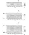
図1は、本発明の一実施形態の撮像レンズユニットの断面図である。図2は、図1の撮像レンズユニットのレンズアセンブリ部の分解図である。なお、図1および図2において、各レンズ素子の断面のハッチングは省略している。図3は、レンズ素子の遮光部の構成を模式的に示す図である。図4は、撮像レンズユニットにおける光路の一例を示す図であり、(a)および(b)は本実施形態の場合を示し、(c)および(d)は、遮光部を有しないこと以外は(a)および(b)と同一の構造の場合を示す。なお、以下の説明において、便宜上、図1および図2の左側を前方(または物体側)、右側を後方(または像側)と表現しているが、これは各構成要素の相対的な位置関係を示すものであって、絶対的な位置関係を示すものではない。 FIG. 1 is a sectional view of an imaging lens unit according to an embodiment of the present invention. FIG. 2 is an exploded view of a lens assembly portion of the imaging lens unit of FIG. In FIGS. 1 and 2, the cross-sectional hatching of each lens element is omitted. FIG. 3 is a diagram schematically showing the configuration of the light shielding portion of the lens element. FIG. 4 is a diagram illustrating an example of an optical path in the imaging lens unit. (A) and (b) show the case of the present embodiment, and (c) and (d) except that no light shielding portion is provided. The case of the same structure as (a) and (b) is shown. In the following description, for the sake of convenience, the left side of FIGS. 1 and 2 is represented as the front (or the object side), and the right side is represented as the rear (or the image side). And not an absolute positional relationship.
図1に示すように、本実施形態の撮像レンズユニット1は、例えば、携帯情報端末のカメラに搭載され、撮像センサSや赤外線カットフィルターFと組み合わされて用いられる。 As shown in FIG. 1, the
撮像レンズユニット1は、鏡筒2と、鏡筒2に収容されたレンズアセンブリ部7と、を有している。 The
鏡筒2は、不透光性の合成樹脂等で構成されており、前後を開口した円筒状の周壁部3と、周壁部3の前方端部を塞ぐように設けられかつ中央に開口4aが形成された前壁部4と、を一体に有している。前壁部4における後方を向く受け面4bは、光軸Pに対して垂直となるように形成されている。受け面4bには、後述する第1のレンズ素子10が当接される。周壁部3の内周面の後方には、後述するレンズアセンブリ部7を鏡筒2の内側に収容した状態で保持するための環状の固定部材5が接着剤などにより固定される。 The
レンズアセンブリ部7は、前方から後方に向けて順に第1のレンズ素子10、第2のレンズ素子20、第3のレンズ素子30、第4のレンズ素子40および第5のレンズ素子50が重ねられて構成され、第2のレンズ素子20と第3のレンズ素子30の間、第3のレンズ素子30と第4のレンズ素子40の間、第4のレンズ素子40と第5のレンズ素子50の間に遮光板60が配置されている。本実施形態において、第1のレンズ素子10、第2のレンズ素子20、第3のレンズ素子30、第4のレンズ素子40および第5のレンズ素子50は、プラスチックで構成されているが、一部または全部がガラスで構成されていてもよい。また、本実施形態では、5枚のレンズ素子を有する構成であるが、本発明は、2枚以上のレンズ構成であれば適用可能である。 In the
第1のレンズ素子10は、最も前方に配置されており、物体側および像側をともに凸面とするレンズ部11と、そのレンズ部11の周縁に位置するコバ部12と、を一体に有している。コバ部12の物体側には、鏡筒2の受け面4bと当接する、光軸Pに対して垂直となるように形成された当接面13が形成されている。コバ部12の像側には、光軸Pを中心とする内向きの円錐状傾斜面14aおよび円錐状傾斜面14aの外周縁に連接された像側を向く円環状平面14bからなる環状段部14が形成されている。 The
第2のレンズ素子20は、第1のレンズ素子10の像側に隣接して配置されており、物体側を凸面、像側を凹面とするレンズ部21と、そのレンズ部21の周縁に位置するコバ部22と、を一体に有している。コバ部22の物体側には、光軸Pを中心とする外向きの円錐状傾斜面23aおよび円錐状傾斜面23aの外周縁に連接された物体側を向く円環状平面23bからなる環状段部23が形成されている。円錐状傾斜面23aは、第1のレンズ素子10の円錐状傾斜面14aと当接され、円環状平面23bは、第1のレンズ素子10の円環状平面14bと当接されることで、第1のレンズ素子10と第2のレンズ素子20の中心が、光軸P上で一致するように位置合わせされる。コバ部22の像側には、光軸Pを中心とする内向きの円錐状傾斜面24aおよび円錐状傾斜面24aの外周縁に連接された像側を向く円環状平面24bからなる環状段部24が形成されている。 The
第3のレンズ素子30は、第2のレンズ素子20の像側に隣接して配置されており、光軸近傍で物体側と像側とをともに凹面とする両面が非球面形状のレンズ部31と、そのレンズ部31の周縁に位置するコバ部32と、を一体に有している。コバ部32の物体側には、光軸Pを中心とする外向きの円錐状傾斜面33aおよび円錐状傾斜面33aの外周縁に連接された物体側を向く円環状平面33bからなる環状段部33が形成されている。円錐状傾斜面33aは、第2のレンズ素子20の円錐状傾斜面24aと当接され、円環状平面33bは、第2のレンズ素子20の円環状平面24bと当接されることで、第2のレンズ素子20と第3のレンズ素子30の中心が、光軸P上で一致するように位置合わせされる。コバ部32の像側には、光軸Pを中心とする内向きの円錐状傾斜面34aおよび円錐状傾斜面34aの外周縁に連接された像側を向く円環状平面34bからなる環状段部34が形成されている。 The
第4のレンズ素子40は、第3のレンズ素子30の像側に隣接して配置されており、物体側を凹面、像側を凸面とするレンズ部41と、そのレンズ部41の周縁に位置するコバ部42と、を一体に有している。コバ部42の物体側には、光軸Pを中心とする外向きの円錐状傾斜面43aおよび円錐状傾斜面43aの外周縁に連接された物体側を向く円環状平面43bからなる環状段部43が形成されている。また、第4のレンズ素子40は、環状段部43(すなわち、円錐状傾斜面43aおよび円環状平面43b)に遮光部46を有している。円錐状傾斜面43aは、遮光部46を介して第3のレンズ素子30の円錐状傾斜面34aと当接され、円環状平面43bは、遮光部46を介して第3のレンズ素子30の円環状平面34bと当接されることで、第3のレンズ素子30と第4のレンズ素子40の中心が、光軸P上で一致するように位置合わせされる。すなわち、環状段部43は、他のレンズ素子である第3のレンズ素子30と位置合わせするための当接部であり、当該環状段部43には、蒸着膜からなる遮光部46が形成されている。また、コバ部42の像側には、光軸Pを中心とする内向きの円錐状傾斜面44aおよび円錐状傾斜面44aの外周縁に連接された像側を向く円環状平面44bからなる環状段部44が形成されている。 The
第5のレンズ素子50は、第4のレンズ素子40の像側に隣接して配置されており、光軸近傍において物体側を凸面、像側を凹面とする両面非球面のレンズ部51と、そのレンズ部51の周縁に位置するコバ部52と、を有している。コバ部52の物体側には、光軸Pを中心とする外向きの円錐状傾斜面53aおよび円錐状傾斜面53aの外周縁に連接された物体側を向く円環状平面53bとからなる環状段部53が形成されている。円錐状傾斜面53aは、第4のレンズ素子40の円錐状傾斜面44aと当接され、円環状平面53bは、第4のレンズ素子40の円環状平面44bと当接されることで、第4のレンズ素子40と第5のレンズ素子50の中心が光軸P上で一致するように位置合わせされる。コバ部42の像側には、光軸Pを中心とする外向きの円錐状傾斜面54aおよび円錐状傾斜面54aの外周縁に連接された像側を向く円環状平面54bとからなる環状段部54が形成されている。環状段部54には、鏡筒2の周壁部3の内周面に固定された固定部材5が当接される。 The
また、撮像レンズユニット1内に配置された複数の遮光板60は、不透光性の合成樹脂、または遮光加工が施された金属で構成された円環平板状の部材である。本実施形態においては、遮光板60は、第2のレンズ素子20と第3のレンズ素子30との間、第3のレンズ素子30と第4のレンズ素子40との間、および、第4のレンズ素子40と第5のレンズ素子50との間にそれぞれ1枚配置されている。 Further, the plurality of
上述した第1〜第5のレンズ素子のレンズ部およびコバ部の表面には、光の反射を防止するためのARコート(反射防止膜)が施されている。なお、遮光部を備える第4のレンズ素子40におけるARコートは、遮光部46を形成する前に施してもよいし、後に施してもよい。 AR coating (antireflection film) for preventing light reflection is applied to the surfaces of the lens portions and the edge portions of the first to fifth lens elements described above. Note that the AR coating in the
ここで、第4のレンズ素子40に形成された遮光部46について詳細に説明する。遮光部46は、複数の蒸着膜を積層して構成されている。具体的には、図3(a)に示すように、遮光部46は、コバ部42(具体的には、円錐状傾斜面43aおよび円環状平面43b)側から順に、二酸化チタン(TiO2)の蒸着膜であるチタン層461aと、クロム(Cr)の蒸着膜であるクロム層461bと、二酸化チタンの蒸着膜であるチタン層461cとを積層して構成されている。クロム層461bは、遮光性が比較的高いが、単層のみでは高温高湿の環境下で膜割れしやすい特性を有している。一方、チタン層461a、461cは、同じ膜厚で形成した場合、クロム層461bと比較して遮光性は劣り、さらに単層のみでは高温高湿の環境下で膜が剥離しやすい特性を有している。図3(a)に示すようにチタン層461a、461cとクロム層461bとを交互に積層した3層構造にすることで、割れ、剥離に強い遮光部46が得られる。特に、高温高湿環境下で使用する場合には、このような積層構造を採ることで信頼性の課題を解決することができる。Here, the
または、上記遮光部46に代えて、図3(b)に示す遮光部46Aを採用してもよい。この遮光部46Aは、上記遮光部46を間に挟むように酸化シリコン(SiO2)の蒸着膜であるシリコン層462a、462bを積層した5層構造で構成されている。すなわち、遮光部46Aは、チタン層とクロム層が交互に積層された3層からなる構造をさらにシリコン層462a、462bで挟んだ5層構造である。シリコン層462a、462bは、遮光部46Aに進入した光(光線)の反射を効果的に抑制する。Alternatively, instead of the
または、上記遮光部46に代えて、図3(c)に示す遮光部46Bを採用してもよい。この遮光部46Bは、上記遮光部46と同様にしてチタン層461a、クロム層461b、チタン層461c、クロム層461dおよびチタン層461eが交互に積層された5層構造であり、さらに、これら5層を挟むようにシリコン層462a、462bとを積層した7層構造で構成されている。このように、蒸着膜を増やすことによって、より遮光性の向上が図られる。なお、この構成において、中央のチタン層461cは、TiO2の蒸着膜に代えてTiO3の蒸着膜を採用してもよい。Alternatively, instead of the
なお、遮光部46は、使用する環境に応じて、チタンもしくはチタン酸化物またはクロムからなる単層の蒸着膜で構成してもよいし、チタン層とクロム層とを交互に積層した2層以上の複数の蒸着膜で構成してもよい。また、遮光部46は、レンズの光学有効部を除くコバ部42に全体的に形成されていてもよい。このような遮光部は、上記第4のレンズ素子40の環状段部43に限らず、第1のレンズ素子10の環状段部14、第2のレンズ素子20の環状段部23、24、第3のレンズ素子30の環状段部33、34、第4のレンズ素子40の環状段部43、44および第5のレンズ素子50環状段部53のいずれかまたは全てに設けられていてもよい。このような遮光部は、レンズアセンブリ部7の構造的な要因で不要光が透過する箇所に選択的に設けることで、ゴーストやフレアの抑制に効果的に寄与する。 The light-shielding
本実施形態において、遮光部46の厚みは、50nm以上であることが好ましい。特に、クロム層461bの膜厚は50nm以上であることが好ましく、チタン層461a、461cの膜厚は400nm以上であることが好ましい。このようにすることで、遮光性を効果的に確保することができる。また、遮光部46の透過率は50%以下であり、反射率は20%以下であることが好ましい。このようにすることで、遮光性を確保するとともに光の反射を抑制して、結像性能の低下を効果的に抑制できる。また、チタン層として、チタン(Ti)またはチタン酸化物(TiO3)の蒸着膜を採用してもよい。シリコン層462a、462bに代えて、フッ化マグネシウムの蒸着膜(MgF2)からなる層を採用してもよい。In the present embodiment, the thickness of the
次に、上述した本実施形態における作用効果について、図4を参照して説明する。 Next, the effect in this embodiment mentioned above is demonstrated with reference to FIG.
図4(a)に示すように、本実施形態の撮像レンズユニット1では、光線Lが、鏡筒2の開口4aに進入し、第1のレンズ素子10を透過して第2のレンズ素子20内を進み、第2のレンズ素子20の像側面で反射されてコバ部22に向かう。すると、この光線Lが、さらに第2のレンズ素子20のコバ部22から第3のレンズ素子30のコバ部32に進むが、第4のレンズ素子40の遮光部46に進路を遮られて撮像センサSに到達することはない。一方、図4(c)に示すように、第4のレンズ素子40に遮光部46が設けられていない撮像レンズユニット801では、光線Lが撮像センサSまで到達して、ゴーストやフレアが発生してしまう。 As shown in FIG. 4A, in the
また、図4(b)に示すように、本実施形態の撮像レンズユニット1では、光線Lが、鏡筒2の開口4aに進入し、各レンズ素子を透過して撮像センサSまで進み、撮像センサSの撮像面で反射されて、第5のレンズ素子50を透過して、第4のレンズ素子40のコバ部42に向かうが、第4のレンズ素子40の遮光部46に進路を遮られて第3のレンズ素子のコバ部32に進むことはない。一方、図4(d)に示すように、第4のレンズ素子に遮光部46が設けられていない撮像レンズユニット801では、光線Lが、第3のレンズ素子30のコバ部32および第2のレンズ素子20のコバ部22を経由して、再度、撮像センサSまで到達して、ゴーストやフレアが発生してしまう。 As shown in FIG. 4B, in the
以上より、本実施形態の撮像レンズユニット1によれば、第4のレンズ素子40のコバ部42の環状段部43、すなわち、第3のレンズ素子30との当接部に遮光部46を均一の厚さで形成することができる。そのため、レンズ素子の位置合わせ精度を低下させることなく、当接部を透過する不要光を遮ることができる。これにより、レンズ素子間の光軸合わせの精度を維持するとともにゴーストやフレアの発生を効果的に抑制できる。また、遮光部46に蒸着工法を採用することで、量産性を高めることができる。 As described above, according to the
上記に本発明の実施形態を説明したが、本発明はこれらの例に限定されるものではない。前述の実施形態に対して、当業者が適宜、構成要素の追加、削除、設計変更を行ったものも、本発明の要旨を備えている限り、本発明の範囲に含まれる。 Although the embodiments of the present invention have been described above, the present invention is not limited to these examples. Those in which those skilled in the art appropriately added, deleted, and changed the design of the above-described embodiments are also included in the scope of the present invention as long as they include the gist of the present invention.
(性能評価)
次に、本発明の撮像レンズユニットの実施例1〜3および比較例1を作成して、結像性能(遮光性)および信頼性について評価を行った。(Performance evaluation)
Next, Examples 1 to 3 and Comparative Example 1 of the imaging lens unit of the present invention were created and evaluated for imaging performance (light shielding property) and reliability.
(実施例1)
上述した実施形態の撮像レンズユニット1において、遮光部46を以下の構成とした。
チタン層461a :TiO2の蒸着膜
クロム層461b :Crの蒸着膜
チタン層461c :TiO2の蒸着膜Example 1
In the
(実施例2)
上記実施例1において、遮光部46に代えて、図3(b)に示す5層構成の遮光部46Aを採用し、遮光部46Aを以下の構成とした。
シリコン層462a :SiO2の蒸着膜
チタン層461a :TiO2の蒸着膜
クロム層461b :Crの蒸着膜
チタン層461c :TiO2の蒸着膜
シリコン層462b :SiO2の蒸着膜(Example 2)
In the first embodiment, instead of the
(実施例3)
上記実施例1において、遮光部46に代えて、単層のチタン層からなる遮光部を採用し、この遮光部を以下の構成とした。
チタン層 :TiO2の蒸着膜(Example 3)
In Example 1, instead of the
Titanium layer: TiO2 deposited film
(比較例1)
上記実施例1において、遮光部46を省略した以外は上記実施例1と同一の構成とした。(Comparative Example 1)
In the first embodiment, the configuration is the same as that of the first embodiment except that the
(結像性能評価試験)
実施例1〜実施例3および比較例1の撮像レンズユニットを、赤外線カットフィルターおよび撮像センサと組み合わせてカメラユニットを構成し、このカメラユニットで撮像した画像のゴーストの有無を確認した。判定基準を以下に示す。
◎・・・ゴーストまたはフレアの発生なし
×・・・ゴーストまたはフレアの発生あり(Imaging performance evaluation test)
The imaging lens units of Examples 1 to 3 and Comparative Example 1 were combined with an infrared cut filter and an imaging sensor to constitute a camera unit, and the presence / absence of a ghost in an image captured by this camera unit was confirmed. Judgment criteria are shown below.
◎ ・ ・ ・ No ghost or flare generated × ・ ・ ・ Ghost or flare generated
(信頼性評価試験)
実施例1〜実施例3の撮像レンズユニットに対し、高温高湿放置試験(85℃−90%RH−500時間)、および低温放置試験(−40℃−500時間)を実施し、遮光部の劣化の有無、および結像性能(ゴースト、フレアの発生)について確認した。判定基準を以下に示す。
◎・・・遮光部の剥離なし、および結像性能に影響するゴースト、フレアの発生なし
○・・・遮光部に結像性能に影響しないわずかな剥離あり
×・・・遮光部に結像性能に影響する剥離あり(Reliability evaluation test)
A high-temperature and high-humidity storage test (85 ° C.-90% RH-500 hours) and a low-temperature storage test (−40 ° C.-500 hours) were performed on the imaging lens units of Examples 1 to 3, and The presence or absence of deterioration and imaging performance (ghost and flare generation) were confirmed. Judgment criteria are shown below.
◎ ・ ・ ・ No peeling of the light shielding part and no ghost or flare that affects the imaging performance ○ ・ ・ ・ Slight peeling that does not affect the imaging performance at the light shielding part × ・ ・ ・ Imaging performance at the light shielding part There is peeling that affects
総合評価の判定基準を以下に示す。
◎・・・結像性能および信頼性ともに良好(◎)
○・・・結像性能および信頼性について不良(×)はないが、可(○)を含む
×・・・結像性能および信頼性について不良(×)を含む
また、総合評価結果を表1に示す。The criteria for comprehensive evaluation are shown below.
◎ ・ ・ ・ Both imaging performance and reliability are good (◎)
○: There is no defect (×) in the imaging performance and reliability, but includes yes (○). ×: Includes a defect (×) in imaging performance and reliability. Table 1 shows the overall evaluation results. Shown in

表1から明らかなように、実施例1および実施例2については、結像性能および信頼性がともに良好であり、高温高湿および低温の環境下においても長期間にわたって良好な結像性能を得ることができた。また、実施例3についても、良好な結像性能を得ることができた。一方、比較例1については、ゴーストの発生を抑制することができず、良好な結像性能を得ることができなかった。このように、評価結果からも本願発明の作用効果が明らかとなった。 As is apparent from Table 1, the imaging performance and reliability of both Example 1 and Example 2 are good, and good imaging performance is obtained over a long period of time even in a high temperature and high humidity environment. I was able to. Also, good imaging performance could be obtained for Example 3. On the other hand, in Comparative Example 1, it was not possible to suppress the occurrence of ghost, and good imaging performance could not be obtained. Thus, the effect of this invention became clear also from the evaluation result.
1…撮像レンズユニット
2…鏡筒
3…周壁部
4…前壁部
4a…開口
4b…受け面
5…固定部材
7…レンズアセンブリ部
10…第1のレンズ素子
20…第2のレンズ素子
30…第3のレンズ素子
40…第4のレンズ素子
50…第5のレンズ素子
11、21、31、41、51…レンズ部
12、22、32、42、52…コバ部
13…当接面
23、33、43、53…環状段部
14、24、34、44、54…環状段部
23a、33a、43a、53a…円錐状傾斜面
14a、24a、34a、44a、54a…円錐状傾斜面
23b、33b、43b、53b…円環状平面
14b、24b、34b、44b、54b…円環状平面
46、46A、46B…遮光部
461a、461c、461e…チタン層
461b、461d…クロム層
462a、462b…シリコン層
60…遮光板
P…光軸
F…赤外線カットフィルター
S…撮像センサ
L…光線DESCRIPTION OF
Claims (11)
Translated fromJapaneseAn imaging lens unit having a plurality of lens elements, wherein at least one lens element is the lens element according to any one of claims 1 to 10.
Priority Applications (4)
| Application Number | Priority Date | Filing Date | Title |
|---|---|---|---|
| JP2017043746AJP2018146878A (en) | 2017-03-08 | 2017-03-08 | Lens element and image capturing lens unit |
| CN201820309707.4UCN208506340U (en) | 2017-03-08 | 2018-03-07 | Lens member and pick-up lens unit |
| CN201810184900.4ACN108572424A (en) | 2017-03-08 | 2018-03-07 | Lens member and pick-up lens unit |
| US15/915,744US10545350B2 (en) | 2017-03-08 | 2018-03-08 | Lens element and imaging lens unit |
Applications Claiming Priority (1)
| Application Number | Priority Date | Filing Date | Title |
|---|---|---|---|
| JP2017043746AJP2018146878A (en) | 2017-03-08 | 2017-03-08 | Lens element and image capturing lens unit |
Publications (1)
| Publication Number | Publication Date |
|---|---|
| JP2018146878Atrue JP2018146878A (en) | 2018-09-20 |
Family
ID=63576812
Family Applications (1)
| Application Number | Title | Priority Date | Filing Date |
|---|---|---|---|
| JP2017043746APendingJP2018146878A (en) | 2017-03-08 | 2017-03-08 | Lens element and image capturing lens unit |
Country Status (3)
| Country | Link |
|---|---|
| US (1) | US10545350B2 (en) |
| JP (1) | JP2018146878A (en) |
| CN (2) | CN108572424A (en) |
Cited By (6)
| Publication number | Priority date | Publication date | Assignee | Title |
|---|---|---|---|---|
| WO2020022295A1 (en)* | 2018-07-26 | 2020-01-30 | Agc株式会社 | Optical element, optical system, and optical device |
| WO2020138013A1 (en) | 2018-12-28 | 2020-07-02 | 三菱瓦斯化学株式会社 | Optical lens and method for manufacturing same |
| TWI714272B (en)* | 2018-10-09 | 2020-12-21 | 中國商寧波舜宇光電信息有限公司 | Integrated lens barrel, optical lens, camera module and method of assembling the same |
| WO2022235108A1 (en)* | 2021-05-06 | 2022-11-10 | 엘지이노텍 주식회사 | Camera module and vehicle comprising same |
| WO2024058541A1 (en)* | 2022-09-13 | 2024-03-21 | 삼성전자주식회사 | Lens assembly and electronic device comprising same |
| WO2024142623A1 (en)* | 2022-12-26 | 2024-07-04 | 富士フイルム株式会社 | Optical system |
Families Citing this family (9)
| Publication number | Priority date | Publication date | Assignee | Title |
|---|---|---|---|---|
| JP2018146878A (en)* | 2017-03-08 | 2018-09-20 | カンタツ株式会社 | Lens element and image capturing lens unit |
| JP7244217B2 (en)* | 2018-05-23 | 2023-03-22 | 東京晨美光学電子株式会社 | Optical element and imaging lens |
| CN111830674B (en)* | 2019-04-18 | 2022-10-21 | 信泰光学(深圳)有限公司 | Lens barrel |
| US11480760B2 (en) | 2019-04-18 | 2022-10-25 | Sintai Optical (Shenzhen) Co., Ltd. | Lens assembly |
| CN110261981B (en)* | 2019-06-10 | 2021-09-10 | Oppo广东移动通信有限公司 | Lens, camera module and electronic device |
| WO2021101175A1 (en)* | 2019-11-20 | 2021-05-27 | Samsung Electronics Co., Ltd. | Electronic device including camera module |
| CN113064224A (en)* | 2019-12-14 | 2021-07-02 | 三营超精密光电(晋城)有限公司 | Optical film, optical lens, lens module and electronic device |
| TWI728690B (en)* | 2020-02-10 | 2021-05-21 | 大立光電股份有限公司 | Imaging lens assembly, camera module and electronic device |
| US12235409B2 (en)* | 2020-12-23 | 2025-02-25 | Largan Precision Co., Ltd. | Optical lens assembly, imaging apparatus and electronic device |
Citations (12)
| Publication number | Priority date | Publication date | Assignee | Title |
|---|---|---|---|---|
| JP2001230396A (en)* | 2000-02-16 | 2001-08-24 | Toppan Printing Co Ltd | Solid-state imaging device |
| JP2004151624A (en)* | 2002-11-01 | 2004-05-27 | Olympus Corp | Tip optical element for microscope immersion objective |
| JP2008122801A (en)* | 2006-11-14 | 2008-05-29 | Sharp Corp | Combined lens and camera module |
| WO2012098808A1 (en)* | 2011-01-21 | 2012-07-26 | 富士フイルム株式会社 | Stack lens array and lens module |
| WO2013047682A1 (en)* | 2011-09-30 | 2013-04-04 | コニカミノルタアドバンストレイヤー株式会社 | Method for producing imaging lens unit, and imaging lens unit |
| JP2013114235A (en)* | 2011-12-01 | 2013-06-10 | Canon Inc | Optical element, method for manufacturing optical element, optical system, and optical apparatus |
| US20150103407A1 (en)* | 2013-10-16 | 2015-04-16 | Shen-Chieh Chen | Lens, optical imaging lens set and method for forming a lens |
| JP2015200690A (en)* | 2014-04-04 | 2015-11-12 | セイコーエプソン株式会社 | Microlens substrate and electro-optical device |
| WO2015178134A1 (en)* | 2014-05-21 | 2015-11-26 | オリンパス株式会社 | Image capturing unit and endoscope |
| US20160349504A1 (en)* | 2015-05-27 | 2016-12-01 | Samsung Electro-Mechanics Co., Ltd. | Lens module |
| JP2016206326A (en)* | 2015-04-20 | 2016-12-08 | セイコーエプソン株式会社 | Electro-optical device, electronic device, and lens array substrate |
| JP2017032798A (en)* | 2015-07-31 | 2017-02-09 | ソニーセミコンダクタソリューションズ株式会社 | SUBSTRATE WITH LENS, LAMINATED LENS STRUCTURE, CAMERA MODULE, AND MANUFACTURING APPARATUS AND METHOD |
Family Cites Families (37)
| Publication number | Priority date | Publication date | Assignee | Title |
|---|---|---|---|---|
| KR950016237A (en)* | 1993-11-17 | 1995-06-17 | 배순훈 | Optical system |
| CN2329016Y (en)* | 1998-07-02 | 1999-07-14 | 机械工业部沈阳仪器仪表工艺研究所 | Anti-glare eye protector for driver |
| TWI225574B (en)* | 2003-05-01 | 2004-12-21 | Nanya Technology Corp | Photomask structure and method of reducing lens aberration and pattern displacement |
| TWI417593B (en)* | 2008-08-18 | 2013-12-01 | Asia Optical Co Inc | Lens set with chimeric structure |
| CN101726822B (en)* | 2008-10-30 | 2012-05-16 | 鸿富锦精密工业(深圳)有限公司 | lens group |
| CN101738648A (en)* | 2008-11-10 | 2010-06-16 | 鸿富锦精密工业(深圳)有限公司 | Lens and manufacturing method thereof |
| KR101476817B1 (en)* | 2009-07-03 | 2014-12-26 | 가부시키가이샤 한도오따이 에네루기 켄큐쇼 | Display device including transistor and manufacturing method thereof |
| CN102004277B (en)* | 2009-08-31 | 2013-11-06 | 鸿富锦精密工业(深圳)有限公司 | Filtering element manufacturing method |
| CN102053325B (en)* | 2009-10-30 | 2013-07-31 | 鸿富锦精密工业(深圳)有限公司 | Lens module |
| JP4943493B2 (en)* | 2009-12-04 | 2012-05-30 | シャープ株式会社 | Optical scanning apparatus and image forming apparatus having the same |
| CN102109650B (en)* | 2009-12-28 | 2014-02-19 | 鸿富锦精密工业(深圳)有限公司 | Preparation method of lens module |
| TW201137489A (en)* | 2010-04-28 | 2011-11-01 | Hon Hai Prec Ind Co Ltd | Light blocking member, method for making same and lens module having same |
| JP5599093B2 (en)* | 2010-05-17 | 2014-10-01 | カンタツ株式会社 | Optical system lens and lens unit using the optical system lens |
| US9163984B2 (en)* | 2011-03-17 | 2015-10-20 | Seiko Epson Corporation | Spectroscopic sensor and angle limiting filter |
| CN106405707B (en)* | 2011-06-06 | 2021-07-20 | Agc株式会社 | Optical filter, solid-state imaging element, lens for imaging device, and imaging device |
| TWI509280B (en)* | 2011-07-28 | 2015-11-21 | Hon Hai Prec Ind Co Ltd | Lens module |
| TWI506329B (en)* | 2011-07-28 | 2015-11-01 | Hon Hai Prec Ind Co Ltd | Lens module |
| TW201307935A (en)* | 2011-08-02 | 2013-02-16 | Hon Hai Prec Ind Co Ltd | Camera module |
| TW201310104A (en)* | 2011-08-29 | 2013-03-01 | Hon Hai Prec Ind Co Ltd | Lens module |
| JP5877206B2 (en)* | 2011-09-30 | 2016-03-02 | 富士フイルム株式会社 | Lens unit and manufacturing method thereof |
| CN103377873B (en)* | 2012-04-27 | 2017-04-12 | 株式会社杰士汤浅国际 | Dielectric barrier discharge lamp |
| KR101444526B1 (en)* | 2012-07-27 | 2014-09-24 | 삼성전기주식회사 | Lens module |
| TW201411217A (en)* | 2012-09-14 | 2014-03-16 | Hon Hai Prec Ind Co Ltd | Lens module |
| US8967814B2 (en)* | 2012-10-16 | 2015-03-03 | Genius Electronic Optical Co., Ltd. | Imaging lens with enhancement of blocking stray light |
| CN103852851A (en)* | 2012-12-06 | 2014-06-11 | 玉晶光电(厦门)有限公司 | Imaging lens capable of eliminating stray light |
| KR101444585B1 (en)* | 2013-03-06 | 2014-09-24 | 삼성전기주식회사 | Lens module |
| JP5807139B2 (en)* | 2013-03-26 | 2015-11-10 | 富士フイルム株式会社 | OPTICAL LENS, MANUFACTURING METHOD THEREOF, LENS UNIT, IMAGING MODULE, ELECTRONIC DEVICE |
| JP6317954B2 (en)* | 2013-10-15 | 2018-04-25 | 富士フイルム株式会社 | Lens unit, imaging module, and electronic device |
| JP6035450B2 (en)* | 2014-03-03 | 2016-11-30 | 富士フイルム株式会社 | Optical element manufacturing method |
| TWI682190B (en)* | 2014-03-19 | 2020-01-11 | 日商豪雅冠得光電股份有限公司 | Optical element |
| JP2015225102A (en) | 2014-05-26 | 2015-12-14 | コニカミノルタ株式会社 | Image capturing lens, image capturing device, and portable terminal |
| US10139669B2 (en)* | 2014-10-15 | 2018-11-27 | Seiko Epson Corporation | Electro-optical device and electronic instrument |
| TWI581030B (en)* | 2015-04-27 | 2017-05-01 | 大立光電股份有限公司 | Optical lens assembly and electronic device |
| TWM521747U (en)* | 2015-10-16 | 2016-05-11 | 大立光電股份有限公司 | Light blocking sheet, light blocking element, optical element, imaging lens assembly and lens module |
| TWM520143U (en) | 2015-12-17 | 2016-04-11 | 大立光電股份有限公司 | Imaging lens module and electronic device |
| TWM527093U (en)* | 2016-02-05 | 2016-08-11 | 大立光電股份有限公司 | Photographing module and electronic device |
| JP2018146878A (en)* | 2017-03-08 | 2018-09-20 | カンタツ株式会社 | Lens element and image capturing lens unit |
- 2017
- 2017-03-08JPJP2017043746Apatent/JP2018146878A/enactivePending
- 2018
- 2018-03-07CNCN201810184900.4Apatent/CN108572424A/enactivePending
- 2018-03-07CNCN201820309707.4Upatent/CN208506340U/enactiveActive
- 2018-03-08USUS15/915,744patent/US10545350B2/enactiveActive
Patent Citations (12)
| Publication number | Priority date | Publication date | Assignee | Title |
|---|---|---|---|---|
| JP2001230396A (en)* | 2000-02-16 | 2001-08-24 | Toppan Printing Co Ltd | Solid-state imaging device |
| JP2004151624A (en)* | 2002-11-01 | 2004-05-27 | Olympus Corp | Tip optical element for microscope immersion objective |
| JP2008122801A (en)* | 2006-11-14 | 2008-05-29 | Sharp Corp | Combined lens and camera module |
| WO2012098808A1 (en)* | 2011-01-21 | 2012-07-26 | 富士フイルム株式会社 | Stack lens array and lens module |
| WO2013047682A1 (en)* | 2011-09-30 | 2013-04-04 | コニカミノルタアドバンストレイヤー株式会社 | Method for producing imaging lens unit, and imaging lens unit |
| JP2013114235A (en)* | 2011-12-01 | 2013-06-10 | Canon Inc | Optical element, method for manufacturing optical element, optical system, and optical apparatus |
| US20150103407A1 (en)* | 2013-10-16 | 2015-04-16 | Shen-Chieh Chen | Lens, optical imaging lens set and method for forming a lens |
| JP2015200690A (en)* | 2014-04-04 | 2015-11-12 | セイコーエプソン株式会社 | Microlens substrate and electro-optical device |
| WO2015178134A1 (en)* | 2014-05-21 | 2015-11-26 | オリンパス株式会社 | Image capturing unit and endoscope |
| JP2016206326A (en)* | 2015-04-20 | 2016-12-08 | セイコーエプソン株式会社 | Electro-optical device, electronic device, and lens array substrate |
| US20160349504A1 (en)* | 2015-05-27 | 2016-12-01 | Samsung Electro-Mechanics Co., Ltd. | Lens module |
| JP2017032798A (en)* | 2015-07-31 | 2017-02-09 | ソニーセミコンダクタソリューションズ株式会社 | SUBSTRATE WITH LENS, LAMINATED LENS STRUCTURE, CAMERA MODULE, AND MANUFACTURING APPARATUS AND METHOD |
Cited By (9)
| Publication number | Priority date | Publication date | Assignee | Title |
|---|---|---|---|---|
| WO2020022295A1 (en)* | 2018-07-26 | 2020-01-30 | Agc株式会社 | Optical element, optical system, and optical device |
| JPWO2020022295A1 (en)* | 2018-07-26 | 2021-08-02 | Agc株式会社 | Optical elements, optics, and optics |
| TWI714272B (en)* | 2018-10-09 | 2020-12-21 | 中國商寧波舜宇光電信息有限公司 | Integrated lens barrel, optical lens, camera module and method of assembling the same |
| WO2020138013A1 (en) | 2018-12-28 | 2020-07-02 | 三菱瓦斯化学株式会社 | Optical lens and method for manufacturing same |
| KR20210109517A (en) | 2018-12-28 | 2021-09-06 | 미츠비시 가스 가가쿠 가부시키가이샤 | Optical lens and manufacturing method thereof |
| US11960056B2 (en) | 2018-12-28 | 2024-04-16 | Mitsubishi Gas Chemical Company, Inc. | Optical lens and method for manufacturing same |
| WO2022235108A1 (en)* | 2021-05-06 | 2022-11-10 | 엘지이노텍 주식회사 | Camera module and vehicle comprising same |
| WO2024058541A1 (en)* | 2022-09-13 | 2024-03-21 | 삼성전자주식회사 | Lens assembly and electronic device comprising same |
| WO2024142623A1 (en)* | 2022-12-26 | 2024-07-04 | 富士フイルム株式会社 | Optical system |
Also Published As
| Publication number | Publication date |
|---|---|
| US20190049737A1 (en) | 2019-02-14 |
| US10545350B2 (en) | 2020-01-28 |
| CN108572424A (en) | 2018-09-25 |
| CN208506340U (en) | 2019-02-15 |
Similar Documents
| Publication | Publication Date | Title |
|---|---|---|
| JP2018146878A (en) | Lens element and image capturing lens unit | |
| JP5896061B1 (en) | Optical system and imaging system | |
| JP7005584B2 (en) | Lens and its manufacturing method and lens module | |
| KR102104081B1 (en) | Camera structure, information and communication equipment | |
| US20130057957A1 (en) | Lens module with anti-reflection film | |
| US20200233176A1 (en) | Camera lens, lens module, and electronic device including the same | |
| JP2007206172A (en) | Imaging system optical element | |
| JP7644580B2 (en) | Lens units and camera modules | |
| JP4768995B2 (en) | Optical filter and imaging device | |
| JPWO2018062298A1 (en) | Lens unit and imaging device | |
| TW202129386A (en) | Shading sheet, lens module, and electronic device | |
| CN114815138B (en) | Imaging lens group and optical identification system | |
| US8520301B2 (en) | Lens module with filter element | |
| JP2013114103A (en) | Optical system and optical equipment | |
| JP2021096283A (en) | Lens system | |
| JP2022162423A (en) | lens with barrel | |
| US12164081B2 (en) | Optical element, optical system, and optical apparatus | |
| JP2004258494A (en) | Nd filter | |
| US11513440B2 (en) | Optical element, optical system, and optical apparatus | |
| JP6539995B2 (en) | Cover member and solid-state imaging device | |
| JPH09288240A (en) | Visual field direction changing optical system for endoscope | |
| JPH0516003B2 (en) | ||
| CN114967025B (en) | Spacer ring and lens module | |
| JP5292137B2 (en) | Antireflection film and optical element | |
| JP7721249B2 (en) | Film-coated lens, lens unit and camera module |
Legal Events
| Date | Code | Title | Description |
|---|---|---|---|
| A621 | Written request for application examination | Free format text:JAPANESE INTERMEDIATE CODE: A621 Effective date:20181004 | |
| A871 | Explanation of circumstances concerning accelerated examination | Free format text:JAPANESE INTERMEDIATE CODE: A871 Effective date:20181004 | |
| A975 | Report on accelerated examination | Free format text:JAPANESE INTERMEDIATE CODE: A971005 Effective date:20181210 | |
| A131 | Notification of reasons for refusal | Free format text:JAPANESE INTERMEDIATE CODE: A131 Effective date:20181218 | |
| A521 | Request for written amendment filed | Free format text:JAPANESE INTERMEDIATE CODE: A523 Effective date:20190129 | |
| A131 | Notification of reasons for refusal | Free format text:JAPANESE INTERMEDIATE CODE: A131 Effective date:20190402 | |
| A02 | Decision of refusal | Free format text:JAPANESE INTERMEDIATE CODE: A02 Effective date:20190710 |