JP2018082150A - Dual channel shower head with improved profile - Google Patents
Dual channel shower head with improved profileDownload PDFInfo
- Publication number
- JP2018082150A JP2018082150AJP2017171674AJP2017171674AJP2018082150AJP 2018082150 AJP2018082150 AJP 2018082150AJP 2017171674 AJP2017171674 AJP 2017171674AJP 2017171674 AJP2017171674 AJP 2017171674AJP 2018082150 AJP2018082150 AJP 2018082150A
- Authority
- JP
- Japan
- Prior art keywords
- showerhead
- plate
- chamber
- apertures
- processing chamber
- Prior art date
- Legal status (The legal status is an assumption and is not a legal conclusion. Google has not performed a legal analysis and makes no representation as to the accuracy of the status listed.)
- Granted
Links
Images


Classifications
- H—ELECTRICITY
- H01—ELECTRIC ELEMENTS
- H01L—SEMICONDUCTOR DEVICES NOT COVERED BY CLASS H10
- H01L21/00—Processes or apparatus adapted for the manufacture or treatment of semiconductor or solid state devices or of parts thereof
- H01L21/67—Apparatus specially adapted for handling semiconductor or electric solid state devices during manufacture or treatment thereof; Apparatus specially adapted for handling wafers during manufacture or treatment of semiconductor or electric solid state devices or components ; Apparatus not specifically provided for elsewhere
- H01L21/67005—Apparatus not specifically provided for elsewhere
- H01L21/67011—Apparatus for manufacture or treatment
- H01L21/67017—Apparatus for fluid treatment
- H01L21/67063—Apparatus for fluid treatment for etching
- H01L21/67069—Apparatus for fluid treatment for etching for drying etching
- H—ELECTRICITY
- H01—ELECTRIC ELEMENTS
- H01J—ELECTRIC DISCHARGE TUBES OR DISCHARGE LAMPS
- H01J37/00—Discharge tubes with provision for introducing objects or material to be exposed to the discharge, e.g. for the purpose of examination or processing thereof
- H01J37/32—Gas-filled discharge tubes
- H01J37/32431—Constructional details of the reactor
- H01J37/3244—Gas supply means
- B—PERFORMING OPERATIONS; TRANSPORTING
- B05—SPRAYING OR ATOMISING IN GENERAL; APPLYING FLUENT MATERIALS TO SURFACES, IN GENERAL
- B05B—SPRAYING APPARATUS; ATOMISING APPARATUS; NOZZLES
- B05B13/00—Machines or plants for applying liquids or other fluent materials to surfaces of objects or other work by spraying, not covered by groups B05B1/00 - B05B11/00
- B05B13/02—Means for supporting work; Arrangement or mounting of spray heads; Adaptation or arrangement of means for feeding work
- B05B13/0278—Arrangement or mounting of spray heads
- H—ELECTRICITY
- H01—ELECTRIC ELEMENTS
- H01J—ELECTRIC DISCHARGE TUBES OR DISCHARGE LAMPS
- H01J37/00—Discharge tubes with provision for introducing objects or material to be exposed to the discharge, e.g. for the purpose of examination or processing thereof
- H01J37/32—Gas-filled discharge tubes
- H01J37/32009—Arrangements for generation of plasma specially adapted for examination or treatment of objects, e.g. plasma sources
- H01J37/32082—Radio frequency generated discharge
- H01J37/32091—Radio frequency generated discharge the radio frequency energy being capacitively coupled to the plasma
- H—ELECTRICITY
- H01—ELECTRIC ELEMENTS
- H01J—ELECTRIC DISCHARGE TUBES OR DISCHARGE LAMPS
- H01J37/00—Discharge tubes with provision for introducing objects or material to be exposed to the discharge, e.g. for the purpose of examination or processing thereof
- H01J37/32—Gas-filled discharge tubes
- H01J37/32431—Constructional details of the reactor
- H01J37/32532—Electrodes
- H01J37/32568—Relative arrangement or disposition of electrodes; moving means
- H—ELECTRICITY
- H01—ELECTRIC ELEMENTS
- H01J—ELECTRIC DISCHARGE TUBES OR DISCHARGE LAMPS
- H01J37/00—Discharge tubes with provision for introducing objects or material to be exposed to the discharge, e.g. for the purpose of examination or processing thereof
- H01J37/32—Gas-filled discharge tubes
- H01J37/32431—Constructional details of the reactor
- H01J37/32715—Workpiece holder
- H—ELECTRICITY
- H01—ELECTRIC ELEMENTS
- H01L—SEMICONDUCTOR DEVICES NOT COVERED BY CLASS H10
- H01L21/00—Processes or apparatus adapted for the manufacture or treatment of semiconductor or solid state devices or of parts thereof
- H01L21/02—Manufacture or treatment of semiconductor devices or of parts thereof
- H01L21/04—Manufacture or treatment of semiconductor devices or of parts thereof the devices having potential barriers, e.g. a PN junction, depletion layer or carrier concentration layer
- H01L21/18—Manufacture or treatment of semiconductor devices or of parts thereof the devices having potential barriers, e.g. a PN junction, depletion layer or carrier concentration layer the devices having semiconductor bodies comprising elements of Group IV of the Periodic Table or AIIIBV compounds with or without impurities, e.g. doping materials
- H01L21/30—Treatment of semiconductor bodies using processes or apparatus not provided for in groups H01L21/20 - H01L21/26
- H01L21/302—Treatment of semiconductor bodies using processes or apparatus not provided for in groups H01L21/20 - H01L21/26 to change their surface-physical characteristics or shape, e.g. etching, polishing, cutting
- H01L21/306—Chemical or electrical treatment, e.g. electrolytic etching
- H01L21/3065—Plasma etching; Reactive-ion etching
- C—CHEMISTRY; METALLURGY
- C23—COATING METALLIC MATERIAL; COATING MATERIAL WITH METALLIC MATERIAL; CHEMICAL SURFACE TREATMENT; DIFFUSION TREATMENT OF METALLIC MATERIAL; COATING BY VACUUM EVAPORATION, BY SPUTTERING, BY ION IMPLANTATION OR BY CHEMICAL VAPOUR DEPOSITION, IN GENERAL; INHIBITING CORROSION OF METALLIC MATERIAL OR INCRUSTATION IN GENERAL
- C23C—COATING METALLIC MATERIAL; COATING MATERIAL WITH METALLIC MATERIAL; SURFACE TREATMENT OF METALLIC MATERIAL BY DIFFUSION INTO THE SURFACE, BY CHEMICAL CONVERSION OR SUBSTITUTION; COATING BY VACUUM EVAPORATION, BY SPUTTERING, BY ION IMPLANTATION OR BY CHEMICAL VAPOUR DEPOSITION, IN GENERAL
- C23C16/00—Chemical coating by decomposition of gaseous compounds, without leaving reaction products of surface material in the coating, i.e. chemical vapour deposition [CVD] processes
- C23C16/44—Chemical coating by decomposition of gaseous compounds, without leaving reaction products of surface material in the coating, i.e. chemical vapour deposition [CVD] processes characterised by the method of coating
- C23C16/455—Chemical coating by decomposition of gaseous compounds, without leaving reaction products of surface material in the coating, i.e. chemical vapour deposition [CVD] processes characterised by the method of coating characterised by the method used for introducing gases into reaction chamber or for modifying gas flows in reaction chamber
- C23C16/45563—Gas nozzles
- C23C16/45565—Shower nozzles
- C—CHEMISTRY; METALLURGY
- C23—COATING METALLIC MATERIAL; COATING MATERIAL WITH METALLIC MATERIAL; CHEMICAL SURFACE TREATMENT; DIFFUSION TREATMENT OF METALLIC MATERIAL; COATING BY VACUUM EVAPORATION, BY SPUTTERING, BY ION IMPLANTATION OR BY CHEMICAL VAPOUR DEPOSITION, IN GENERAL; INHIBITING CORROSION OF METALLIC MATERIAL OR INCRUSTATION IN GENERAL
- C23C—COATING METALLIC MATERIAL; COATING MATERIAL WITH METALLIC MATERIAL; SURFACE TREATMENT OF METALLIC MATERIAL BY DIFFUSION INTO THE SURFACE, BY CHEMICAL CONVERSION OR SUBSTITUTION; COATING BY VACUUM EVAPORATION, BY SPUTTERING, BY ION IMPLANTATION OR BY CHEMICAL VAPOUR DEPOSITION, IN GENERAL
- C23C16/00—Chemical coating by decomposition of gaseous compounds, without leaving reaction products of surface material in the coating, i.e. chemical vapour deposition [CVD] processes
- C23C16/44—Chemical coating by decomposition of gaseous compounds, without leaving reaction products of surface material in the coating, i.e. chemical vapour deposition [CVD] processes characterised by the method of coating
- C23C16/50—Chemical coating by decomposition of gaseous compounds, without leaving reaction products of surface material in the coating, i.e. chemical vapour deposition [CVD] processes characterised by the method of coating using electric discharges
- C23C16/503—Chemical coating by decomposition of gaseous compounds, without leaving reaction products of surface material in the coating, i.e. chemical vapour deposition [CVD] processes characterised by the method of coating using electric discharges using DC or AC discharges
- C—CHEMISTRY; METALLURGY
- C23—COATING METALLIC MATERIAL; COATING MATERIAL WITH METALLIC MATERIAL; CHEMICAL SURFACE TREATMENT; DIFFUSION TREATMENT OF METALLIC MATERIAL; COATING BY VACUUM EVAPORATION, BY SPUTTERING, BY ION IMPLANTATION OR BY CHEMICAL VAPOUR DEPOSITION, IN GENERAL; INHIBITING CORROSION OF METALLIC MATERIAL OR INCRUSTATION IN GENERAL
- C23C—COATING METALLIC MATERIAL; COATING MATERIAL WITH METALLIC MATERIAL; SURFACE TREATMENT OF METALLIC MATERIAL BY DIFFUSION INTO THE SURFACE, BY CHEMICAL CONVERSION OR SUBSTITUTION; COATING BY VACUUM EVAPORATION, BY SPUTTERING, BY ION IMPLANTATION OR BY CHEMICAL VAPOUR DEPOSITION, IN GENERAL
- C23C16/00—Chemical coating by decomposition of gaseous compounds, without leaving reaction products of surface material in the coating, i.e. chemical vapour deposition [CVD] processes
- C23C16/44—Chemical coating by decomposition of gaseous compounds, without leaving reaction products of surface material in the coating, i.e. chemical vapour deposition [CVD] processes characterised by the method of coating
- C23C16/50—Chemical coating by decomposition of gaseous compounds, without leaving reaction products of surface material in the coating, i.e. chemical vapour deposition [CVD] processes characterised by the method of coating using electric discharges
- C23C16/505—Chemical coating by decomposition of gaseous compounds, without leaving reaction products of surface material in the coating, i.e. chemical vapour deposition [CVD] processes characterised by the method of coating using electric discharges using radio frequency discharges
- H—ELECTRICITY
- H01—ELECTRIC ELEMENTS
- H01J—ELECTRIC DISCHARGE TUBES OR DISCHARGE LAMPS
- H01J2237/00—Discharge tubes exposing object to beam, e.g. for analysis treatment, etching, imaging
- H01J2237/32—Processing objects by plasma generation
- H01J2237/33—Processing objects by plasma generation characterised by the type of processing
- H01J2237/334—Etching
- H—ELECTRICITY
- H01—ELECTRIC ELEMENTS
- H01L—SEMICONDUCTOR DEVICES NOT COVERED BY CLASS H10
- H01L21/00—Processes or apparatus adapted for the manufacture or treatment of semiconductor or solid state devices or of parts thereof
- H01L21/67—Apparatus specially adapted for handling semiconductor or electric solid state devices during manufacture or treatment thereof; Apparatus specially adapted for handling wafers during manufacture or treatment of semiconductor or electric solid state devices or components ; Apparatus not specifically provided for elsewhere
- H01L21/67005—Apparatus not specifically provided for elsewhere
- H01L21/67011—Apparatus for manufacture or treatment
- H01L21/67155—Apparatus for manufacturing or treating in a plurality of work-stations
- H01L21/6719—Apparatus for manufacturing or treating in a plurality of work-stations characterized by the construction of the processing chambers, e.g. modular processing chambers
Landscapes
- Engineering & Computer Science (AREA)
- Physics & Mathematics (AREA)
- Plasma & Fusion (AREA)
- Chemical & Material Sciences (AREA)
- Analytical Chemistry (AREA)
- Computer Hardware Design (AREA)
- General Physics & Mathematics (AREA)
- Manufacturing & Machinery (AREA)
- Condensed Matter Physics & Semiconductors (AREA)
- Microelectronics & Electronic Packaging (AREA)
- Power Engineering (AREA)
- Drying Of Semiconductors (AREA)
- Plasma Technology (AREA)
- Chemical Vapour Deposition (AREA)
- Electromagnetism (AREA)
- Spectroscopy & Molecular Physics (AREA)
- Paper (AREA)
Abstract
Translated fromJapaneseDescription
Translated fromJapanese 関連出願の相互参照
[0001]本出願は、2016年10月4日に出願された、「DUAL−CHANNEL SHOWERHEAD WITH IMPROVED PROFILE」なる名称の、米国特許出願第15/285,331号の利益を主張し、これによって、あらゆる目的において参照によりその全体が本明細書に組み込まれる。CROSS REFERENCE TO RELATED APPLICATIONS [0001] This application claims the benefit of US patent application Ser. No. 15 / 285,331, filed Oct. 4, 2016, entitled “DUAL-CHANNEL SHOWERHEAD WITH IMPROVED PROFILE”. Which is hereby incorporated by reference in its entirety for all purposes.
[0002]本発明の技術は、半導体システム、プロセス及び機器に関する。より具体的には、本発明の技術は、プラズマ電極として使用されるシャワーヘッドを含む処理チャンバに関する。 [0002] The techniques of the present invention relate to semiconductor systems, processes and equipment. More specifically, the technique of the present invention relates to a processing chamber that includes a showerhead used as a plasma electrode.
[0003]集積回路は、基板表面上に複雑にパターン形成された材料層を形成するプロセスによって可能になる。基板上にパターン形成された材料を形成するには、露出した材料を取り除くための制御された方法が必要である。化学エッチングは、下位層にフォトレジストでパターンを転写する、層を薄くする、又は表面にすでにある特徴の横寸法を薄くすることを含む、様々な目的に使用される。多くの場合、1つの材料を別の材料よりも早くエッチングして、例えばパターン転写プロセスを促進するエッチングプロセスを有することが望ましい。上記エッチングプロセスは、第1の材料に対して選択的であると言われる。材料、回路、及びプロセスに多様性があるために、様々な材料に対して選択性を有するエッチングプロセスが開発されてきた。 [0003] Integrated circuits are enabled by the process of forming intricately patterned material layers on the substrate surface. Forming patterned material on a substrate requires a controlled method to remove exposed material. Chemical etching is used for a variety of purposes, including transferring a pattern with a photoresist to a sublayer, thinning a layer, or thinning the lateral dimensions of features already on the surface. In many cases, it is desirable to have an etching process that etches one material faster than another, e.g., to facilitate the pattern transfer process. The etching process is said to be selective for the first material. Because of the diversity of materials, circuits, and processes, etching processes that are selective to various materials have been developed.
[0004]エッチングプロセス、堆積プロセス、及び洗浄プロセスは、様々なチャンバで実行され得る。これらのチャンバは、容量結合プラズマを形成するために使用される構成要素を含み、又は、例えば、誘導結合されたプラズマなど、他の形態のプラズマが形成される内側チャンバ領域に近接し得る。チャンバ構成要素は、チャンバを通してプラズマ発生又は前駆体供給の効果を低減するための何らかの方法で構成されるが、これは、追加の機能性を犠牲にする可能性がある。 [0004] Etching processes, deposition processes, and cleaning processes may be performed in various chambers. These chambers may include components used to form capacitively coupled plasma or may be proximate to an inner chamber region where other forms of plasma are formed, such as, for example, inductively coupled plasma. The chamber components are configured in some way to reduce the effects of plasma generation or precursor delivery through the chamber, but this may sacrifice additional functionality.
[0005]したがって、高品質のデバイス及び構造を形成するために使用することができる改良されたシステム及び方法が必要とされる。これらの必要性及び他の必要性が、本発明の技術によって対処される。 [0005] Accordingly, there is a need for improved systems and methods that can be used to form high quality devices and structures. These needs and other needs are addressed by the techniques of the present invention.
[0006]本発明の技術による半導体処理システム及び方法は、半導体処理チャンバの内部領域を少なくとも部分的に画定する、リッドを含むチャンバハウジングを含む半導体処理チャンバを含み得る。チャンバは、チャンバの処理領域内で基板を支持するように構成されたペデスタルを含み得る。チャンバは、リッドと処理領域との間に位置付けられた第1のシャワーヘッドを含み、第1のシャワーヘッドと半導体処理チャンバの処理領域との間に位置付けられた面板を含み得る。チャンバはまた、面板と半導体処理チャンバの処理領域との間のチャンバ内に位置付けられた第2のシャワーヘッドを含み得る。第2のシャワーヘッドは、少なくとも2つの板の間に空間を画定するように連結された少なくとも2つの板を含み得る。少なくとも2つの板は、第2のシャワーヘッドを通るチャネルを少なくとも部分的に画定し、各チャネルは、チャネルの第1の端で第1の直径によって特徴付けられ、チャネルの第2の端で複数のポートによって特徴付けられ得る。 [0006] Semiconductor processing systems and methods according to the techniques of the present invention may include a semiconductor processing chamber including a chamber housing including a lid that at least partially defines an interior region of the semiconductor processing chamber. The chamber can include a pedestal configured to support a substrate within the processing region of the chamber. The chamber includes a first showerhead positioned between the lid and the processing region, and may include a face plate positioned between the first showerhead and the processing region of the semiconductor processing chamber. The chamber may also include a second showerhead positioned in the chamber between the face plate and the processing region of the semiconductor processing chamber. The second showerhead can include at least two plates coupled to define a space between the at least two plates. The at least two plates at least partially define a channel through the second showerhead, each channel being characterized by a first diameter at the first end of the channel and a plurality at the second end of the channel. Can be characterized by ports.
[0007]実施形態では、各ポートは、第1の直径未満の直径によって特徴付けられ得る。加えて、第1のシャワーヘッドは、電源に連結され、面板は、電気的接地に連結され得る。例示的半導体処理チャンバはまた、第1のシャワーヘッドと面板との間にスペーサを含み得る。第1のシャワーヘッド、面板、及びスペーサは、半導体処理チャンバ内にプラズマ処理領域を少なくとも部分的に画定するように構成され得る。幾つかの実施形態では、ペデスタルは、電源に連結され、第2のシャワーヘッドは、電気的接地に連結され得る。ペデスタル及び第2のシャワーヘッドは、半導体処理チャンバの処理領域内にプラズマ処理領域を少なくとも部分的に画定するように構成され得る。実施形態において、面板及び第2のシャワーヘッドは、直接接触しており、かつその双方が電気的接地に連結され得る。 [0007] In an embodiment, each port may be characterized by a diameter less than the first diameter. In addition, the first showerhead can be coupled to a power source and the faceplate can be coupled to electrical ground. The exemplary semiconductor processing chamber may also include a spacer between the first showerhead and the faceplate. The first showerhead, faceplate, and spacer may be configured to at least partially define a plasma processing region within the semiconductor processing chamber. In some embodiments, the pedestal can be coupled to a power source and the second showerhead can be coupled to electrical ground. The pedestal and the second showerhead may be configured to at least partially define a plasma processing region within the processing region of the semiconductor processing chamber. In an embodiment, the faceplate and the second showerhead are in direct contact, and both can be connected to electrical ground.
[0008]第2のシャワーヘッドが、面板に面する各チャネルの第1の端を有し、かつ半導体処理チャンバの処理領域に近接した各チャネルの第2の端を有するチャンバ内に位置付けられ得る。加えて、第2のシャワーヘッドは、半導体処理チャンバの処理領域に近接した各チャネルの第1の端を有し、かつ面板に面する各チャネルの第2の端を有するチャンバ内に位置付けられ得る。第2のシャワーヘッドの表面は、半導体処理チャンバの処理領域に隣接し、表面は、コーティング又は処理され得る。幾つかの実施形態では、第1の直径は、少なくとも約2.5mmであり、各ポートの直径は、約1.2mm以下であり得る。 [0008] A second showerhead may be positioned in the chamber having a first end of each channel facing the faceplate and having a second end of each channel proximate to a processing region of the semiconductor processing chamber. . In addition, the second showerhead may be positioned in a chamber having a first end of each channel proximate to a processing region of the semiconductor processing chamber and having a second end of each channel facing the faceplate. . The surface of the second showerhead is adjacent to the processing region of the semiconductor processing chamber and the surface can be coated or processed. In some embodiments, the first diameter is at least about 2.5 mm and the diameter of each port can be about 1.2 mm or less.
[0009]本発明の技術はまた、シャワーヘッドを包囲する。シャワーヘッドは、複数の通り孔を画定する第1の板を含み得る。シャワーヘッドはまた、第1の板に連結された第2の板を含み得る。第2の板は、第1の複数の開孔及び第2の複数の開孔を画定し、第2の複数の開孔は、第2の複数の開孔のうちの少なくとも2つの開孔を含む複数の群の開孔の第2の板に画定され得る。幾つかの実施形態では、第1の板の各通り孔は、チャネルを形成するために少なくとも1つの群の開孔と位置合わせされ得る。 [0009] The technique of the present invention also surrounds the showerhead. The showerhead may include a first plate that defines a plurality of through holes. The showerhead can also include a second plate coupled to the first plate. The second plate defines a first plurality of apertures and a second plurality of apertures, and the second plurality of apertures defines at least two apertures of the second plurality of apertures. A plurality of groups of apertures may be defined in the second plate. In some embodiments, each through-hole in the first plate can be aligned with at least one group of apertures to form a channel.
[0010]実施形態では、第1の板及び第2の板は、第1の板と第2の板との間に空間を画定するために互いに連結され得る。空間は、第2の板の第1の複数の開孔から流体的にアクセス可能であり、チャネルは、第1の板と第2の板との間に画定された空間から流体的に分離され得る。第1の複数の開孔は、第1の複数の開孔のうちの少なくとも2つの開孔を含む複数の第1群の開孔の第2の板に画定され、各第1群の開孔は、第2の複数の開孔のうちの1つの群の開孔を取り囲み得る。幾つかの実施形態では、各第1群の開孔は、少なくとも4つの開孔を含み得る。幾つかの実施形態では、各通り孔は、少なくとも約5mmの直径によって特徴付けられ得る。第2の複数の開孔のうちの各開孔は、約1mm以下の直径によって特徴付けられ得る。第2の複数の開孔のうちの各群の開孔は、少なくとも約6つの開孔を含み得る。幾つかの実施形態では、第2の板は、プラズマ劣化に耐性のある材料を含み得る。 [0010] In an embodiment, the first plate and the second plate may be coupled together to define a space between the first plate and the second plate. The space is fluidly accessible from the first plurality of apertures in the second plate, and the channel is fluidly separated from the space defined between the first plate and the second plate. obtain. The first plurality of apertures are defined in a second plate of the plurality of first group of apertures including at least two apertures of the first plurality of apertures, each first group of apertures. May surround a group of apertures of the second plurality of apertures. In some embodiments, each first group of apertures can include at least four apertures. In some embodiments, each through hole may be characterized by a diameter of at least about 5 mm. Each aperture of the second plurality of apertures may be characterized by a diameter of about 1 mm or less. Each group of apertures in the second plurality of apertures may include at least about six apertures. In some embodiments, the second plate can include a material that is resistant to plasma degradation.
[0011]本発明の技術はまた、第1の複数の開孔を画定する第1の板を含み得る、シャワーヘッドを包囲し得る。第1の複数の開孔は、第1の複数の開孔のうちの少なくとも2つの開孔を含む複数の群の開孔の第1の板に画定され得る。シャワーヘッドはまた、第1の板に連結された第2の板を含み得る。第2の板は、第2の複数の開孔及び複数の通り孔を画定し、第2の板の各通り孔は、チャネルを形成するために第1の複数の開孔のうちの少なくとも1つの群の開孔と位置合わせされ得る。 [0011] The techniques of the present invention may also enclose a showerhead, which may include a first plate that defines a first plurality of apertures. The first plurality of apertures may be defined in a first plate of the plurality of groups of apertures including at least two apertures of the first plurality of apertures. The showerhead can also include a second plate coupled to the first plate. The second plate defines a second plurality of apertures and a plurality of through holes, wherein each through hole of the second plate is at least one of the first plurality of apertures to form a channel. Can be aligned with two groups of apertures.
[0012]そのような技術は、従来のシステム及び技術よりも多数の利点を提供し得る。例えば、本技術のシャワーヘッドは、プラズマ漏出を制限し得る改良された接地経路を提供し得る。加えて、シャワーヘッドは、反応副生成物が逆流し、他のチャンバ構成要素と接触するのを制限し得る。これら多数の利点及び特徴と共に、これらの実施形態及びその他の実施形態を、下記の説明及び添付の図面と合わせてさらに詳細に説明する。 [0012] Such techniques may provide a number of advantages over conventional systems and techniques. For example, a showerhead of the present technology may provide an improved ground path that can limit plasma leakage. In addition, the showerhead can limit reaction by-products from flowing back and contacting other chamber components. Together with these numerous advantages and features, these and other embodiments are described in further detail in conjunction with the following description and the accompanying drawings.
[0013]本開示の技術の性質及び利点は、本明細書の残りの部分と図面を参照することによって更に理解され得る。 [0013] The nature and advantages of the techniques of this disclosure may be further understood with reference to the remaining portions of the specification and drawings.
[0026]図の幾つかは、概略図として含まれている。図面は例示のためのものであり、縮尺について特に規定されていない限り、正しい縮尺と見なすべきではないことに留意されたい。加えて、概略図として、図面は、理解を促すために提供されており、実際の描写表現と比べると態様又は情報をすべて含んでいるわけではなく、例示手目的で追加の材料又は強調された材料を含むこともある。 [0026] Some of the figures are included as schematics. It should be noted that the drawings are for illustration purposes only and should not be considered as true scale unless scale is specifically defined. In addition, as a schematic, the drawings are provided for ease of understanding and do not include all aspects or information as compared to the actual depiction, but have additional material or emphasis for illustrative purposes. May contain material.
[0027]添付図面では、類似の構成要素及び/又は特徴は、同一の参照符号を有し得る。更に、同類の様々な構成要素は、類似の構成要素を区別する文字により、参照符号に従って区別されることがある。第1の参照符号のみが本明細書において使用されている場合、その説明は、文字に関わりなく、同じ第1の参照符号を有する類似の構成要素のうちの任意の1つに適用可能である。 [0027] In the accompanying drawings, similar components and / or features may have the same reference number. Furthermore, various similar components may be distinguished according to reference signs by letters that distinguish similar components. Where only the first reference number is used herein, the description is applicable to any one of the similar components having the same first reference number, regardless of the letter. .
[0028]本発明の技術は、調整したエッチング処理を含む半導体処理のためのシステム及び構成要素を含む。利用可能なある処理チャンバは、複数のプラズマ機構、例えばウエハレベルにおける機構や遠隔プラズマ源などを含み得る。ウエハレベルでのプラズマは、2つの電極間に形成された容量結合プラズマを介して形成され得ることが多い。これらの電極の一方又は両方は、シャワーヘッド、ペデスタル、又はチャンバ壁などの追加のチャンバ構成要素であってもよく、又はこれらを含んでもよい。シャワーヘッドは、前駆体分配に影響を及ぼすための任意の数の方法で構成され、またプラズマ発生の際に電極として使用されてもよい。しかしながら、処理チャンバでフロープロファイルを改善するためのシャワーヘッド構成は、電極としてのシャワーヘッドの性能に影響を与えることがある。 [0028] The techniques of the present invention include systems and components for semiconductor processing, including tailored etching processes. Some processing chambers that may be utilized may include multiple plasma features, such as wafer level features or remote plasma sources. The wafer level plasma can often be formed via a capacitively coupled plasma formed between two electrodes. One or both of these electrodes may be or include additional chamber components such as a showerhead, pedestal, or chamber wall. The showerhead may be configured in any number of ways to affect precursor distribution and may be used as an electrode during plasma generation. However, a showerhead configuration to improve the flow profile in the processing chamber can affect the performance of the showerhead as an electrode.
[0029]例えば、シャワーヘッドを通る開口の直径が増大すると、シャワーヘッドを通るフローの均一性だけではなくラジカルの再結合の改善も可能になり得る。他方で、シャワーヘッドが電極として動作している場合、開口直径の増大により、シャワーヘッドを通してプラズマが漏出する可能性があり、次いで他の構成要素と相互に作用することがある。ウエハレベルプラズマについて、より大きな開孔直径によって、エッチング又は堆積反応からの反応副生成物が、開孔を通って逆流し、他のチャンバ構成要素と接触、堆積、又は反応することも可能になろう。 [0029] For example, increasing the diameter of the opening through the showerhead may allow for improved recombination of radicals as well as flow uniformity through the showerhead. On the other hand, if the showerhead is operating as an electrode, the increase in aperture diameter can cause the plasma to leak through the showerhead and then interact with other components. For wafer level plasma, the larger aperture diameter also allows reaction byproducts from the etching or deposition reaction to flow back through the aperture and contact, deposit, or react with other chamber components. Let's go.
[0030]従来の技術は、多数の方法でこれらの現象を取り扱ってきた可能性がある。1つの例では、シャワーヘッドを介した材料の任意の逆流を防止又は低減するために、追加の板又はシャワーヘッドが処理領域に含まれていた。しかしながら、そのような構成要素は、前駆体のためのチャンバフロー経路を増加させ得る。チャンバを通って移動するラジカル前駆体にとって、このことは、エネルギーの再結合又は損失の発生を可能にし、前駆体又はプラズマ廃水の有効性を低減する可能性がある。本発明の技術は、ウエハレベルのプラズマ発生との使用を目的とすることを含む、半導体処理チャンバで利用され得る改良されたシャワーヘッドを提供することによって、これらの欠陥を克服し得る。シャワーヘッドは、十分な前駆体フローを可能にするために一端に増大した直径を有するチャネルを含み、プラズマ及び反応副生成物がシャワーヘッドを介して逆流するのを防止するために、反対の端にポートを含み得る。これらの設計は、他のチャンバ構成要素を保護する一方で、またラジカル再結合速度への効果を制限し得る。 [0030] The prior art may have handled these phenomena in a number of ways. In one example, additional plates or showerheads were included in the processing area to prevent or reduce any backflow of material through the showerhead. However, such components can increase the chamber flow path for the precursor. For radical precursors that move through the chamber, this may allow energy recombination or loss to occur, reducing the effectiveness of the precursor or plasma wastewater. The techniques of the present invention can overcome these deficiencies by providing an improved showerhead that can be utilized in semiconductor processing chambers, including for use with wafer level plasma generation. The showerhead includes a channel with an increased diameter at one end to allow sufficient precursor flow, and the opposite end to prevent plasma and reaction byproducts from flowing back through the showerhead. May include ports. These designs can protect other chamber components while also limiting the effect on radical recombination rates.
[0031]残りの開示内容は、本発明の技術を利用した特定のエッチング処理を規定通りに識別するものであるが、システム及び方法は、記載されたチャンバで起こりうる堆積及び洗浄プロセスに等しく適用可能であることは、容易に理解できることである。したがって、この技術は、エッチング処理のみでの使用に限定されるものと考えるべきではない。 [0031] Although the remaining disclosure routinely identifies specific etching processes utilizing the techniques of the present invention, the system and method are equally applicable to deposition and cleaning processes that may occur in the described chamber. It is easy to understand what is possible. Therefore, this technique should not be considered limited to use with only etching processes.
[0032]図1は、実施形態による、堆積チャンバ、エッチングチャンバ、ベーキングチャンバ、及び硬化チャンバの処理システム100の1つの実施形態の上面図を示す。図1に示される処理ツール100は、複数の処理チャンバ114A−D、移送チャンバ110、サービスチャンバ116、一体型計測チャンバ117、及び一対のロードロックチャンバ106A−Bを含有し得る。処理チャンバは、追加の処理チャンバに加え、図2に関して記載されるものに類似の構造又は構成要素を含み得る。 [0032] FIG. 1 illustrates a top view of one embodiment of a
[0033]チャンバの間で基板を輸送するために、移送チャンバ110は、ロボット輸送機構113を含有し得る。輸送機構113は、延長可能なアーム113Bの遠位端にそれぞれ取り付けられた一対の基板輸送ブレード113Aを有し得る。ブレード113Aは、個々の基板を処理チャンバに及び処理チャンバから運ぶために使用され得る。動作中に、輸送機構113のブレード113Aなどの基板輸送ブレードの1つが、チャンバ106A−Bなどのロードロックチャンバの1つから基板Wを回収し、例えば、チャンバ114A−Dにおける以下に記載されるエッチング処理などの第1段階の処理に基板Wを運び得る。チャンバが使用中の場合、ロボットは、処理が完了するまで待機し、次いで処理した基板を1つのブレード113Aによりチャンバから除去し、第2のブレード(図示されず)で新しい基板を挿入し得る。基板はいったん処理されると、次に第2段階の処理に移動し得る。移動毎に、輸送機構113は、一般的に、基板を運ぶ1つのブレードと、基板交換を実行するための1つの空のブレードとを有し得る。移送機構113は、交換が遂行可能となるまで各チャンバで待機し得る。 [0033] In order to transport substrates between chambers, the
[0034]処理チャンバ内で処理がいったん完了すると、輸送機構113は、基板Wを最後の処理チャンバから移動させ、基板Wをロードロックチャンバ106A−B内のカセットに輸送し得る。ロードロックチャンバ106A−Bから、基板はファクトリインターフェース104内に移動し得る。ファクトリインターフェース104は、一般的に、大気圧清浄環境のポッドローダ105A−Dとロードロックチャンバ106A−Bとの間で基板を移送するために動作し得る。ファクトリインターフェース104の清浄環境は、一般的に、例えばHEPAろ過などの空気ろ過処理を介して提供され得る。ファクトリインターフェース104はまた、処理前に基板を正しく位置合わせするために使用され得る基板オリエンタ/アライナ(図示されず)を含み得る。ロボット108A−Bなどの少なくとも1つの基板ロボットは、ファクトリインターフェース104内の種々の位置/場所の間とそれらに連通する他の場所に基板を輸送するために、ファクトリインターフェース104の中に位置付けら得る。ロボット108A−Bは、ファクトリインターフェース104の第1の端から第2の端まで筐体104内を軌道システムに沿って移動するように構成され得る。 [0034] Once processing is complete in the processing chamber, the
[0035]処理システム100は、処理チャンバで実行されている処理の何れかにわたって適応性のある制御を提供し得る、制御信号を提供するために、一体型計測チャンバ117を更に含み得る。一体型計測チャンバ117は、厚さ、粗さ、組成など、種々の膜特性を測定するために種々の計測デバイスの何れかを含み得、計測デバイスは、更に、自動化された方法で、真空下での限界寸法、側壁角度、及び特徴高さ等の格子パラメータを特徴付けることができる。 [0035] The
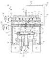
[0036]ここで図2を参照すると、本発明の技術による例示的処理チャンバシステム200の断面図が示される。チャンバ200は、例えば、先ほど検討されたシステム100の処理チャンバセクション114のうちの一又は複数で使用され得る。一般的に、エッチングチャンバ200は、イオンミリング動作を実施するための第1の容量結合プラズマ源と、エッチング動作及びオプションの堆積動作を実施するための第2の容量結合プラズマ源とを含み得る。チャンバ200は、チャック250を取り囲む接地チャンバ壁240を含み得る。実施形態において、既知であろう他のクランプ機構が用いられてもよいが、チャック250は、処理中にチャック250の上面に基板202を締める静電チャックであり得る。チャック250は、埋め込まれた熱交換コイル217を含み得る。例示的実施形態では、熱交換コイル217は、チャック250の温度、及び最終的には基板202の温度を制御するために、エチレングリコール/水混合物などの熱移送流体がそれを介して通過し得るような一又は複数の熱移送流体チャネルを含む。 [0036] Referring now to FIG. 2, a cross-sectional view of an exemplary
[0037]チャック250は、メッシュ249が基板202の静電気的クランプを実施するためにDCバイアス電位を運び得るように、高圧DC供給248に結合されたメッシュ249を含み得る。チャック250は、第1のRF電源に結合され得、そのような1つの実施形態では、メッシュ249は、DC電圧オフセット及びRF電圧電位の双方が、チャック250の上面の薄い誘電体層全域で結合されるように、第1のRF電源に結合され得る。例示的実施形態では、第1のRF電源は、第1及び第2のRF発生器252、253を含み得る。RF発生器252、253は、任意の産業上利用される周波数で動作し得るが、例示的実施形態では、RF発生器252は、有利な方向性を提供するために60MHzで動作し得る。第2のRF発生器253も提供される場合、例示的周波数は、2MHzであり得る。 [0037] The
[0038]RF電力供給されるチャック250により、RFリターン経路が、デュアルチャネルシャワーヘッドを含み得る第1のシャワーヘッド225によって提供され得る。第1のシャワーヘッド225は、第1のシャワーヘッド225及びチャンバ壁240によって画定された第1のチャンバ領域284内に第1の供給ガスを分散させるためにチャックの上に配置され得る。したがって、チャック250及び第1のシャワーヘッド225は、第1のチャンバ領域284内の第1の供給ガスの第1のプラズマ270に容量性のエネルギーを与えるために第1のRF結合電極ペアを形成する。RF電力供給されたチャックの容量性の結合から生じる、DCプラズマバイアス、又はRFバイアスは、イオンミリングプラズマを供給するために、例えば、第1の供給ガスがArであるArイオンなどのイオンフラックスを第1のプラズマ270から基板202に生成し得る。第1のシャワーヘッド225は、接地されてもよく、又は交互に、例えば13.56MHz又は60MHzなどの、チャック250以外の周波数で動作可能な一又は複数の発生器を有するRF源228に結合されてもよい。図示された実施形態では、第1のシャワーヘッド225は、例えばコントローラ(図示されず)によって、エッチング処理中に自動的に制御され得るリレー227を通して、接地又はRF源228に選択可能に結合され得る。開示された実施形態では、チャンバ200は、シャワーヘッド225又は誘電体スペーサ220を含まなくてもよく、その代わりに、更に以下に記載されるバッフル215及びシャワーヘッド210のみを含んでいてもよい。 [0038] With an RF powered
[0039]図に更に示されるように、エッチングチャンバ200は、低い処理圧力で高いスループットが可能なポンプスタックを含み得る。実施形態において、少なくとも1つのターボ分子ポンプ265、266は、一又は複数のゲートバルブ260を通して第1のチャンバ領域284に結合され、第1のシャワーヘッド225に対向するチャック250の下に配置され得る。ターボ分子ポンプ265、266は、適切なスループットを有している任意の市販のポンプであり、より具体的には、例えば、アルゴンが第1の供給ガスである場合、50sccmから500sccmまでのArなど、第1の供給ガスの所望の流量で約10mTorr以下又は約5mTorr以下に処理ガスを維持するために適切にサイズ決定され得る。図示された実施形態では、チャック250は、2つのターボポンプ265と266との間で中心に置かれるペデスタルの一部を形成し得るが、代替構成では、チャック250は、チャック250の中心に位置合わせされた中心を有する単一のターボ分子ポンプを含むチャンバ壁240から一端が飛び出したペデスタルの上にあってもよい。 [0039] As further shown in the figure, the
[0040]第2のシャワーヘッド120は、第1のシャワーヘッド225の上に配置され得る。1つの実施形態では、処理中に、例えば、ガス供給システム290から供給されたアルゴンなどの第1の供給ガス源は、ガス注入口276に結合され得、第1の供給ガスは、第2のシャワーヘッド210を通って延びる複数の開孔280を介して第2のチャンバ領域281内へ、及び第1のシャワーヘッド225を通って延びる複数の開孔282を介して第1のチャンバ領域284内へ流れる。開孔278を有する追加の流れ分散器又はバッフル215は、分散領域218を通ってエッチングチャンバ200の直径全域に第1の供給ガス流216を更に分散させ得る。代替的実施形態では、第1の供給ガスは、点線223によって示されるように、第2のチャンバ領域281から分離した開孔283を介して、第1のチャンバ領域284内に直接流れ得る。 [0040] The second showerhead 120 may be disposed on the
[0041]チャンバ200は、加えて、エッチング動作を実行するために図示された状態から再構成されてもよい。二次的電極205が第1のシャワーヘッド225の上方に配置され得、第2のチャンバ領域281がそれらの間に存在する。二次的電極205は、エッチングチャンバ200のリッド又は上面板を更に形成し得る。二次的電極205及び第1のシャワーヘッド225は、第2のチャンバ領域281内で第2の供給ガスの第2のプラズマ292を容量的に放電するために、誘電体リング220によって電気的に絶縁され、第2のRF結合電極ペアを形成し得る。有利には、第2のプラズマ292は、チャック250の上にかなりのRFバイアス電位を供給しなくてもよい。第2のRF結合電極ペアの少なくとも1つの電極は、エッチングプラズマにエネルギーを与えるためにRF源に結合され得る。二次的電極205は、第2のシャワーヘッド210に電気的に結合され得る。例示的実施形態では、第1のシャワーヘッド225は、接地平面に結合されても浮遊していてもよく、リレー227を通して接地に結合されてもよく、第1のシャワーヘッド225は、動作のイオンミリングモード中にRF電源228によって電力供給も可能になる。第1のシャワーヘッド225が接地される場合、例えば 13.56MHz又は60MHzで作動する一又は複数のRF発生器を有するRF電源208は、二次的電極205をイオンミリング動作中などの他の動作モード中に接地も可能にするリレー207を通して、二次的電極205に結合されるが、二次的電極205はまた、第1のシャワーヘッド225に電力供給される場合には浮遊したままでもよい。 [0041] The
[0042]三フッ化窒素などの第2の供給ガス源、及びアンモニアなどの水素源は、ガス供給システム290から供給され、点線224などを介してガス吸入口276に結合され得る。このモードでは、第2の供給ガスは、第2のシャワーヘッド210を通って流れ、第2のチャンバ領域281においてエネルギーが与えられ得る。反応性核種は、次いで、基板202と反応するために、第1のチャンバ領域284内に移り得る。更に図示されるように、第1のシャワーヘッド225がマルチチャネルシャワーヘッドである実施形態について、一又は複数の供給ガスは、第2のプラズマ292によって生成される反応性核種と反応するように提供され得る。1つの実施形態では、水源が複数の開孔283に結合されてもよい。追加の構成はまた、提供された一般図に基づいてもよいが、種々の構成要素が再構成されてもよい。例えば、流れ分散器又はバッフル215は、第2のシャワーヘッド210に類似した板であってもよく、二次的電極205と第2のシャワーヘッド210との間に位置付けられてもよい。 [0042] A second supply gas source, such as nitrogen trifluoride, and a hydrogen source, such as ammonia, may be supplied from
[0043]これらの板の何れかはプラズマ生成のための様々な構成において電極として動作し得るので、一又は複数の環状又は他の形状のスペーサが、誘電体リング220と同様に、これらの構成要素のうちの一又は複数の間に位置付けられてもよい。第2のシャワーヘッド210はまた、実施形態においてイオン抑制板として動作し得、第2のシャワーヘッド210を通したイオン核種の流れを低減、限定、又は抑制するように構成され得る一方で、中性核種及びラジカル核種の流れをなおも可能にする。一又は複数の追加のシャワーヘッド又は分散器は、第1のシャワーヘッド225とチャック250との間のチャンバ内に含まれ得る。そのようなシャワーヘッドは、先ほど記載された分配板又は構造体の何れかの形状又は構造をとり得る。また、実施形態では、遠隔プラズマユニット(図示されず)は、種々の処理で使用するためにプラズマ放出物をチャンバに提供するようにガス注入口に結合され得る。 [0043] Since any of these plates can act as electrodes in various configurations for plasma generation, one or more annular or other shaped spacers, like the
[0044]実施形態では、チャック250は、距離H2に沿って、第1のシャワーヘッド225に対して垂直な方向に移動可能であり得る。チャック250は、チャック250と第1のシャワーヘッド225との間での熱移送を制御する手段として、第1のシャワーヘッド225に近付く又は遠ざかるように移動できるようにするために、ベローズ255、又はそのようなものによって囲まれた作動機構上にあり、80℃から150℃又はそれ以上の上昇温度となり得る。よって、エッチング処理は、第1のシャワーヘッド225に対する第1及び第2の所定の位置の間でチャック250を移動させることによって、実施され得る。代替的には、チャック250は、エッチング処理中に第1のシャワーヘッド225によって加熱を制御するために、基板202をチャック250の上面から距離H1ほど上昇させるためのリフターを含み得る。エッチング処理が、例えば約90℃から110℃の固定温度で実行される、他の実施形態では、チャック変位機構が回避され得る。システムコントローラ(図示されず)は、自動的に第1及び第2のRF結合電極ペアに交互に電力供給することによって、エッチング処理中に第1及び第2のプラズマ270及び292に交互にエネルギーを与え得る。 [0044] In an embodiment, the
[0045]チャンバ200はまた、堆積動作を実行するために再構成されてもよい。プラズマ292は、第2のプラズマ292について記載された方法の何れかで実施され得るRF放電によって、第2のチャンバ領域281で生成され得る。第1のシャワーヘッド225が堆積中にプラズマ292を生成するために電力供給される場合、第1のシャワーヘッド225は、チャンバ壁に対して電気的に浮遊しているように、誘電体スペーサ230によって接地されたチャンバ壁240から分離され得る。例示的実施形態では、分子酸素などの酸化剤供給ガス源が、ガス供給システム290から供給され、ガス注入口276に結合され得る。第1のシャワーヘッド225がマルチチャネルシャワーヘッドである実施形態では、例えばOMCTSなどの任意のケイ素含有前駆体が、ガス供給システム290から供給され、プラズマ292から第1のシャワーヘッド225を通って移動する反応性核種と反応するように、第1のチャンバ領域284内に方向付けられ得る。代替的には、ケイ素含有前駆体はまた、酸化剤と共にガス注入口276を通って流れ得る。チャンバ200は、本発明の技術に関して検討される種々の動作に用いられ得る一般的チャンバ構成として含まれる。 [0045] The
[0046]図3は、実施形態による処理チャンバで使用するためのシャワーヘッド325の底面図である。シャワーヘッド325は、図2に示されるシャワーヘッド225に対応し得る。第1の流体チャネル又は開孔282の図であり得る通り孔365は、シャワーヘッド225を通る前駆体の流れを制御し影響を与えるように、複数の形状及び構成を有し得る。第2の流体チャネル又は開孔283の図であり得る小さな孔375は、シャワーヘッドの表面に、更には通り孔365の間でさえ、実質的に平らに分散され得、他の構成ではなくシャワーヘッドから出る際に前駆体のより均一な混合を提供し得る。 [0046] FIG. 3 is a bottom view of a
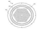
[0047]実施形態による面板用の配置が、図4に示されている。図示されたように、面板400は、貫通孔を含む板又はマニホールドを含み得る。面板のアセンブリは、図3に示されるようなシャワーヘッドに類似してもよく、又は特に前駆体ガスの分配パターン用に構成された設計を含んでいてもよい。面板400は、図2に示されるチャンバなどの例示的処理チャンバ内に種々の配置で位置付けられた環状フレーム410を含み得る。実施形態において、以下に記載されるようなイオン抑制板523に類似し得る板420がフレーム上又は内に結合され得る。実施形態では、面板400は、フレーム410と板420とが単一部品の材料である単一部品設計であり得る。 [0047] An arrangement for a face plate according to an embodiment is shown in FIG. As shown, the
[0048]板は、ディスク形状を有し、フレーム410上又は内に位置し得る。板は、板を前述のようなプラズマ配置で使用するための電極として機能させることができる他の導電性材料だけではなく、アルミニウムを含む金属などの導電性材料であってもよい。板は、様々な厚さであって、板内に画定される複数の開孔465を含み得る。図4に示される例示的配置は、図3の配置を参照しつつ先ほど記載されたパターンを含み、図示されたように六角形などの形状寸法パターンの開孔の一連のリングを含み得る。理解されるように、図示されたパターンは、例示的なものであって、様々なパターン、孔の配置、及び孔の間隔が設計に包含されることを理解すべきである。 [0048] The plate has a disk shape and may be located on or in the
[0049]開孔465は、流体が動作中に開孔を通って流れることができるようにサイズ決定されてもよく、又は別の方法で構成されてもよい。開孔は、種々の実施形態では、約2インチ未満のサイズであり、約1.5インチ以下、約1インチ以下、約0.9インチ以下、約0.8インチ以下、約0.75インチ以下、約0.7インチ以下、約0.65インチ以下、約0.6インチ以下、約0.55インチ以下、約0.5インチ以下、約0.45インチ以下、約0.4インチ以下、約0.35インチ以下、約0.3インチ以下、約0.25以下、約0.2インチ以下、約0.15インチ以下、約0.1インチ以下、約0.05インチ以下、約0.04インチ以下、約0.035インチ以下、約0.03インチ以下、約0.025インチ以下、約0.02インチ以下、約0.015インチ以下、約0.01インチ以下などであり得る。 [0049] The
[0050]幾つかの実施形態では、面板400は、チャンバプラズマ領域からのイオン帯電の核種の移動を抑えるように構成されている構造全域に複数の開孔を画定するイオンサプレッサとして動作しつつ、帯電していない中性又はラジカル核種が、イオンサプレッサを通過して、イオンサプレッサ下流の活性化ガス供給領域内に移動できるようにし得る。実施形態において、イオンサプレッサは、種々の開孔構成を有する貫通孔を含む板であり得る。これらの荷電されていない核種には、開孔を介して反応が弱いキャリアガスと共に輸送される非常に反応性の高い核種が含まれ得る。上述したように、孔を介したイオン核種のマイグレーションが低減され、場合によっては完全に抑制されることがある。例えば、孔のアスペクト比、若しくは孔の長さに対する直径、及び/又は孔の形状寸法は、イオンサプレッサを通る活性化ガスの中のイオン帯電核種の流れが減るように制御され得る。 [0050] In some embodiments, the
[0051]ここで図5を参照すると、本発明の技術による処理チャンバ500の簡略図が示される。システム500のチャンバは、図2から図4までに関して前述の構成要素の何れかを含み、チャンバの処理領域560に半導体基板555を収納するように構成され得る。チャンバハウジング503は、チャンバの内部領域を少なくとも部分的に確定し得る。例えば、チャンバハウジング503は、リッド502を含み、図に示された他の板又は構成要素の何れかを少なくとも部分的に含み得る。例えば、チャンバ構成要素は、チャンバハウジング503の一部を少なくとも部分的に画定する各構成要素を含む一連の積み重ねられた構成要素として含まれてもよい。基板555は、図示したように、ペデスタル565上に位置し得る。処理チャンバ500は、注入口501に結合された遠隔プラズマユニット(図示されず)を含み得る。他の実施形態では、システムは、遠隔プラズマユニットを含まなくてもよい。 [0051] Referring now to FIG. 5, a simplified diagram of a
[0052]遠隔プラズマユニットを含んでも含んでいなくても、システムは、処理チャンバの混合領域511へのアクセスを提供し得る、注入口501を通して前駆体又は他の流体を受容するように構成され得る。混合領域511は、チャンバの処理領域560から分離され、かつ処理領域533に流体結合され得る。混合領域511は、一又は複数の前駆体用の注入口アセンブリを含み得る、チャンバリッド502又はリッドアセンブリなどのシステム500のチャンバの最上部と、下の面板509などの分配デバイスとによって少なくとも部分的に画定され得る。面板509は、開示された実施形態の図3及び図4に図示されたシャワーヘッド又は面板に類似し得る。面板509は、チャンバを介した処理の前に、混合領域511において前駆体の分配及び/又は滞留時間に影響を与えるように位置付けられ及び/又は成形され得る複数のチャネル若しくは開孔507を含み得る。 [0052] The system, whether or not including a remote plasma unit, is configured to receive a precursor or other fluid through an
[0053]例えば、再結合は、面板509全域の開孔数、開孔サイズ、又は開孔の構成を調節することによって、影響を受け、制御され得る。図示されたように、面板509は、混合領域511とチャンバの処理領域560との間に位置付けられ、面板509は、チャンバ500を通して一又は複数の前駆体を分散させるように構成され得る。チャンバ500は、開示された実施形態にオプションで含まれ得る一連の構成要素のうちの一又は複数を含み得る。例えば、面板509が記載されているが、幾つかの実施形態では、チャンバは、そのような面板を含まなくてもよい。開示された実施形態では、混合領域511で少なくとも部分的に混合された前駆体は、チャンバを通り、システムの動作圧、チャンバ構成要素の配置、又は前駆体の流れプロファイルを介して、方向付けられ得る。 [0053] For example, recombination can be affected and controlled by adjusting the number of apertures across the
[0054]チャンバ500は、加えて、第1のシャワーヘッド515を含み得る。シャワーヘッド515は、図3から図4を参照して検討される板の特徴又は特性のうちの何れかを有し得る。シャワーヘッド515は、図示されたように半導体処理チャンバ内に位置付けられ、リッド502と処理領域560との間に含まれ又は位置付けられ得る。実施形態では、シャワーヘッド515は、コーティング、シーズニング、又は他の方法で処理された材料であり得る金属又は伝導構成要素であってもよく、又はそのような構成要素を含んでいてもよい。例示的材料は、アルミニウムを含む金属、並びに酸化アルミニウムを含む金属酸化物を含み得る。用いられている前駆体、又はチャンバ内で実行されている処理次第で、シャワーヘッドは、構造的安定性、並びに用いられ得る伝導性を提供し得る任意の他の金属又は材料であり得る。 [0054] The
[0055]シャワーヘッド515は、シャワーヘッドを通して前駆体の均一な分配を促すために、一又は複数の開孔517を画定し得る。開孔517は、様々な構成又はパターンで含まれてもよく、所望の前駆体分配を提供し得る任意の数の形状寸法によって特徴付けられ得る。シャワーヘッド515は、実施形態において、電源と電気的に連結され得る。例えば、シャワーヘッド515は、図示されたようにRF源519と連結され得る。操作されるとき、RF源519は、容量結合プラズマ(「CCP」)をシャワーヘッド515と別の構成要素との間に形成可能にするシャワーヘッド515に電流を供給し得る。 [0055] The
[0056]追加の面板又はデバイス523は、シャワーヘッド515の下に配置され得る。面板523は、面板509に類似の設計を含み、例えば、図3又は図4に示されたものに類似の配置を有し得る。実施形態において、面板523は、シャワーヘッド515と処理領域560との間の半導体処理チャンバ内に位置付けられ得る。スペーサ510は、シャワーヘッド515と板523との間に位置付けられ、誘電材料を含み得る。開孔524は、板523の中に画定され、板523を通してイオン核種の流れに影響を与えるように分散及び構成され得る。例えば、開孔524は、処理領域560に向かって方向付けられたイオン核種の流れを少なくとも部分的に抑制するように構成され得、板523を前述のイオンサプレッサとして動作可能にさせ得る。開孔524は、前述のようなチャネルを含む様々な形状を有し、開示された実施形態では、処理領域560から外に向かって離れるように延びる先細部分を含み得る。 [0056] An additional faceplate or
[0057]面板523は、電気的接地534に連結され、実施形態では、プラズマを発生し得る。例えば、シャワーヘッド515、面板523、及びスペーサ510は、半導体処理チャンバ内にプラズマ処理領域533を少なくとも部分的に画定し得る。前駆体は、注入口501を介して供給され、面板509及びシャワーヘッド515を介してプラズマ処理領域533に分散され得る。シャワーヘッド515は、面板523で接地に対して充電され、前駆に体は、プラズマ処理領域533内でプラズマを形成するためにエネルギーが与えられ得る。プラズマ廃水は、次いで面板523を通って処理領域560の方に流れ、基板若しくはウエハ555、又は基板上の材料と相互に作用する。 [0057] The
[0058]チャンバ500は、チャンバ内に、第2のシャワーヘッドでもあるガス供給アセンブリ535を更に含み得る。例えば、ガス供給アセンブリ535は、処理領域560を少なくとも部分的に画定し、前駆体をその領域に分散し得る。基板555上に均一の処理を提供するために、ガス供給アセンブリ535は、前駆体のより均一のフローを処理領域560内に提供するように構成され得る。ある態様において前述のデュアルチャネルシャワーヘッドに類似し得るガス供給アセンブリ535は、処理領域560とリッド502との間など、処理領域560上のチャンバ内に位置し、処理領域560と面板523との間などに位置付けられ得る。ガス供給アセンブリ535は、第1及び第2の前駆体の両方を、チャンバの処理領域560の中へ供給するように構成され得る。実施形態では、ガス供給アセンブリ535は、チャンバの内部領域を、遠隔領域と、基板555が位置付けられる処理領域とに少なくとも部分的に分割し得る。 [0058] The
[0059]図5の例示的システムはデュアルチャネルシャワーヘッドを含むが、前駆体を注入口501を通って導入された核種から流動的に分離された状態に維持する代替的分配アセンブリを用いてもよいと理解される。例えば、貫通孔を含む板、及び板の下の管を用いることができるが、他の構成は、効率が低下した状態で動作してもよく、又は記載されたデュアルチャネルシャワーヘッドのように均一の処理として提供されなくてもよい。開示された設計の1つを用いることによって、前駆体は、処理領域560に侵入する前にプラズマによって事前に励起されない処理領域560に導入され得るか、又は前駆体(it)が反応し得る追加の前駆体との接触を回避するように導入され得る。図示されていないが、環状スペーサなどの追加のスペーサは、板を互いから分離させるために、面板523とシャワーヘッド535との間に配置され得る。追加の前駆体が含まれない実施形態では、ガス供給アセンブリ535は、前述の構成要素の何れかに類似の設計を有し、図4に示された面板に類似の特徴を含み得る。 [0059] Although the exemplary system of FIG. 5 includes a dual channel showerhead, an alternative distribution assembly that maintains the precursor in fluid separation from the nuclide introduced through the
[0060]実施形態では、ガス供給アセンブリ535は、例えば、抵抗ヒータ又は温度制御された流体用のチャネルを含み得る、埋め込み式ヒータ539を含み得る。ガス供給アセンブリ535は、実施形態では、上板及び下板を含み、ガス供給アセンブリ535内の構成又は間隔に応じて、約2つ以上の板、約3つ以上の板、約4つ以上の板、約5つ以上の板、又はそれ以上の板を含み得る。板は、板同士の間で空間537を画定するために、互いに結合され得る。上板と下板トを通る第1の流体チャネル540と、下板を通る第2の流体チャネル545を提供するように、板が結合され得る。形成された第2のチャネルは、下板を通して空間537から流体的にアクセスできるように構成され、第1の流体チャネル540は、複数の板と第2の流体チャネル545との間の空間537から流体的に分離させるようにしてもよい。空間537は、前述のチャネル223などのガス供給アセンブリ535の側面を介して流体的にアクセス可能となり得る。チャネルは、チャンバ500の注入口501から分離したチャンバ内のアクセスと連結され得る。 [0060] In an embodiment, the
[0061]ガス供給アセンブリ535は、プラズマ処理動作においても同様に利用され、実施例では、例えば、電気的接地544と電気的に連結され得る。ガス供給アセンブリ535を電気的接地に連結することによって、ガス供給アセンブリ535は、面板523と類似の電位となり、よって、プラズマが2つの構成要素間で形成されるのを防止し得る。幾つかの実施形態では、面板523及びガス供給アセンブリ535は、図示されたように直接接触しており、双方が電気的接地と連結され得る。ペデスタル565は、電源554と連結され、接地されたガス供給アセンブリ535と組み合わせて、半導体処理チャンバの処理領域560内で追加のプラズマ処理領域を少なくとも部分的に画定し得る。ウエハレベルでプラズマ処理能力を提供することによって、プラズマ処理から利益を受けるエッチング及び堆積動作だけではなく、前述の材料改質などの追加の動作が実行され得る。 [0061] The
[0062]幾つかの実施形態では、上述のプラズマは、処理領域560内のプラズマ処理領域内だけではなく、プラズマ処理領域533の中などの処理領域から離れたチャンバの領域で実行され得る。これらのプラズマ領域の各々は、実施形態では、容量結合プラズマであり得るが、誘導結合されたプラズマ領域を提供するためのコイルなど、他のプラズマ発生構成要素が含まれてもよい。プラズマが各々に接触する、面板、シャワーヘッド、チャンバ壁、スペーサ、及びペデスタルは、プラズマが間に形成され得る構成要素の劣化を最小にするために、更にコーティング又はシーズニングされてもよい。板は、更に、劣化又は影響される可能性が低い、セラミック、金属酸化物、又は他の導電性材料を含む組成物を含み得る。 [0062] In some embodiments, the plasma described above can be performed not only in the plasma processing region in the processing region 560, but also in regions of the chamber that are remote from the processing region, such as in the
[0063]従来の容量結合プラズマ(「CCP」)を作用させると、チャンバ構成要素が劣化し、基板上にうっかり分散させた粒子が除去されることがある。そのような粒子は、半導体基板にわたって短絡を起こす可能性がある金属粒子のため、これらの基板から形成されたデバイスの性能に影響を与えることがある。しかしながら、開示された技術のCCPは、実施形態において、低下した又は実質的に低下した電力で作用し、プラズマ領域内のイオン化種の代わりに、遠隔プラズマユニットによって生成されるようなプラズマを維持するために用いられ得る。他の実施形態では、CCPは、領域内に供給された前駆体をイオン化するために作用し得る。例えば、CCPは、約1kW以下、500W以下、250W以下、100W以下、50W以下、20W以下などの電力レベルで作用し得る。更に、CCPは、空間内に均一のプラズマを分配し得る平らなプラズマプロファイルを生成し得る。よって、プラズマ放出物のより均一の流れが、チャンバの処理領域に対して下流で供給され得る。 [0063] When conventional capacitively coupled plasma (“CCP”) is applied, chamber components may degrade and particles that are inadvertently dispersed on the substrate may be removed. Such particles can affect the performance of devices formed from these substrates because of metal particles that can cause a short circuit across the semiconductor substrate. However, the disclosed technology CCP, in embodiments, operates with reduced or substantially reduced power to maintain a plasma as generated by a remote plasma unit instead of ionized species in the plasma region. Can be used for In other embodiments, the CCP can act to ionize the precursor supplied in the region. For example, CCP can operate at power levels of about 1 kW or less, 500 W or less, 250 W or less, 100 W or less, 50 W or less, 20 W or less. Furthermore, the CCP can generate a flat plasma profile that can distribute a uniform plasma in space. Thus, a more uniform flow of plasma emissions can be provided downstream to the processing region of the chamber.
[0064]ウエハレベルでのプラズマ形成は、前述のように処理動作に有利であり得る。しかしながら、ガス供給アセンブリ535などの構成要素がプラズマ処理機器の一部として包含されるとき、プラズマ形成用の追加的検討が含まれることがある。プラズマ廃水がチャンバ領域に供給可能となるように、第1の流体チャネル540が含まれてもよい。十分なフローを提供するために、かつプラズマ廃水との相互作用を低下させるために、チャネルは、例えば、約2.5mm以上などの増大した直径によって特徴付けられ得る。しかしながら、ガス供給アセンブリ535が容量結合プラズマ動作に含まれるとき、これらの開孔サイズは、問題を提起することがある。 [0064] Plasma formation at the wafer level may be advantageous for processing operations as described above. However, when components such as
[0065]例えば、プラズマは一般に、デバイ長より長い領域に形成され得る。第1の流体チャネル540が増大した直径によって特徴付けられるとき、プラズマ処理領域に面するアセンブリの表面は、表面全域にRF連続性を提供しないことがある。その結果、プラズマが第1の流体チャネル540内に生成され、これらのチャネルを通って面板523の方へ逆に漏出し得る。ガス分配アセンブリ535の表面のうちの一又は複数は、プラズマからの劣化を低減するためにコーティング又は処理され得る。同様に、面板523の一又は複数の表面は、プラズマからの劣化を低減するためにコーティング又は処理され得る。しかしながら、各構成要素の上でコーティング又は処理された表面は、互いに向かい合っていなくてもよい。 [0065] For example, the plasma may generally be formed in a region longer than the Debye length. When the first
[0066]例えば、図5に示されるように、処理領域560に向かい合う、近接する、又は隣接するガス供給アセンブリ535の表面は、処理されてもいいが、面板523に向かい合う表面は、コーティング又は処理されなくてもよい。同様に、プラズマ処理領域533に向かい合う、近接する、又は隣接する面板523の表面は、コーティング又は処理されてもいいが、ガス供給アセンブリ535に向かい合う表面は、コーティング又は処理されなくてもよい。したがって、面板523とガス供給アセンブリ535との間の領域内に漏出するプラズマは、構成要素の未処理部分を劣化させる可能性がある。第1の流体チャネル540は、この相互作用を防止するために直径が低減され得るが、そのような低減は、プラズマ処理領域533で生成されたプラズマ廃水の再結合及びプラズマ廃水との相互作用を増加させ得る。別の解決策は、プラズマの逆流を低減するために、ガス供給アセンブリ535とペデスタル565との間に小さな開孔を有する追加のシャワーヘッドを包含することを含み得る。しかしながら、この解決策は、前駆体の移動の長さが増加するため、及び追加のシャワーヘッドがガス供給アセンブリで回避されている同一の再結合をもたらし得るので、ある状況においては受け入れられないことがある。例えば、ある堆積動作において、トリシリルアミン又はNHラジカル若しくはイオンなどのある前駆体の滞留時間は、受け入れ可能な堆積を提供するために制御され、フロー経路は、構成要素上での堆積を防止するために比較的スムーズであり得る。追加のシャワーヘッドを包含することによって、フロー経路長が増大し、かつフロー経路が妨害される可能性がある。 [0066] For example, as shown in FIG. 5, the surface of the
[0067]したがって、本発明の技術は、第1の流体チャネル540それ自体を調節することによって、これらの状況で改善することがある。例えば、本発明の技術によるシャワーヘッド又はガス供給アセンブリは、各チャネルが、チャネルの第1の端で第1の直径によって特徴付けられ、かつチャネルの第2の端で複数のポートによって特徴付けられ得る流体チャネルを含み得る。続く図は、例えば、チャンバ500のガス供給アセンブリ535として使用され得るような、本発明の技術によるチャンバ内で使用され得る例示的シャワーヘッド又はガス供給アセンブリを検討することになる。シャワーヘッドはまた、本開示を通して検討される改善した制御から利益を得る、他のプラズマチャンバを含む、任意の他のチャンバにおいて使用されてもよい。 [0067] Thus, the technique of the present invention may improve in these situations by adjusting the first
[0068]図6Aは、本発明の技術の実施形態による例示的シャワーヘッド600の上面図を示す。シャワーヘッド600は、本開示全体で検討された前述のシャワーヘッド又は面板の何れかの構成要素又は特性の何れかを含み得る。図示されたように、シャワーヘッド600は、第1の板610の表面にわたって複数の通り孔620を画定する第1の板610を含み得る。第1の板610は、アルミニウム、酸化アルミニウム、他の金属、例えば酸化イットリウムなどの他の酸化金属、又は他の処理された又はコーティングされた材料を含み得る導電性材料であり得る、又はそれらを含み得る。通り孔620は、例えば、前述の第1の流体チャネル540の第1の端を示し得る。通り孔620は、例えば、約50mm以下の直径によって特徴付けられ、実施形態では、約40mm以下、約30mm以下、約20mm以下、約15mm以下、約12mm以下、約10mm以下、約9mm以下、約8mm以下、約7mm以下、約6mm以下、約5mm以下、約4mm以下、約3mm以下、約2mm以下、又はそれ以下の直径によって特徴付けられ得る。 [0068] FIG. 6A shows a top view of an
[0069]通り孔620は、前駆体に十分なフロー能力を提供するために、実施形態では、約4mm以上の直径によって特徴付けられ得る。例えば、5mm以下の直径は、チャンバの遠隔領域で生成されたプラズマ廃水を含む、チャンバを通って流れる前駆体の再結合又は他の特性に影響を与え得る。したがって、幾つかの実施形態では、通り孔620の直径は、前駆体又はプラズマ廃水へのより大きな影響を防止するために、約2.5mm以上、約3mm以上、約3.5mm以上、約4mm以上、約4.5mm以上、約5mm以上、約5.5mm以上、約6mm以上、約6.5mm以上、約7mm以上、又はそれ以上に維持され得る。直径はまた、提供又は包含される任意の数の組み合わせであってもよく、定義された範囲の何れかに含まれる範囲であってもよい。シャワーヘッド600及び開孔620のサイズ次第で、第1の板610は、最大で500、500を上回る若しくは約500の開孔を画定し、実施形態では、最大で1000、1000を上回る若しくは約1000の開孔、約2000の開孔、約3000の開孔、約4000の開孔、約5000の開孔、約6000の開孔、約7000の開孔、約8000の開孔、約9000の開孔、約10000の開孔、又はそれ以上を画定し得る。 [0069] The through-
[0070]通り孔620はまた、形成されたチャネルを通って、第1の板610に連結され得る第2の板650までの図を提供し得る。幾つかの実施形態では、シャワーヘッド600は、3以上の板を含んでいてもよく、又は画定された特徴を有する単一の板だけを含んでいてもよい。第2の板650は、第1の板610の通り孔620を通って見えるような、画定されたポート660を含み得る。図6Bは、本発明の技術の実施形態による例示的シャワーヘッド600の底面図を示す。図は、シャワーヘッド600の第2の板650の図を示す。記載されたように、第2の板650は、シャワーヘッド600を介して生成された流体チャネルの第2の端に含まれ得る、第2の板650全域に画定されたポート660を含み得る。幾つかの実施形態では、各ポート660は、通り孔620の直径未満の直径によって特徴付けられ得る。 [0070] The through
[0071]先ほど説明されたように、ポート660は、プラズマがシャワーヘッド600を通って漏出するのを防止し、また局部的プラズマ動作の副生成物がシャワーヘッド600を通って上流に流れるのを防止し得る。したがって、ポート660は、実施形態では、約2mm以下の直径によって特徴付けられ、実施形態において、約1.5mm以下、約1.2mm以下、約1.0mm以下、約0.9mm以下、約0.8mm以下、約0.7mm以下、約0.6mm以下、約0.5mm以下、約0.4mm以下、約0.3mm以下、約0.2mm以下、約0.1mm以下、又はそれ以下の直径によって特徴付けられ得る。例えば、ポート660は、実施形態では、約0.1mmから約1.2mmまでの直径によって位特徴付けられ、実施形態において、約0.2mmから約1mmまでの直径によって特徴付けられ得る。より小さなポート660は、シャワーヘッド600にわたって改善されたRF連続性を提供し、例えば、接地された電極として動作していることがある。改善されたRF連続性は、プラズマをシャワーヘッド600の下に含有可能とし、又は実施形態において、シャワーヘッド600の下に実質的に含有可能となり得る。加えて、より小さなポート660はまた、反応副生成物が通り孔620を通って逆流し、追加の構成要素と接触するのを防止し得る。 [0071] As previously described, the
[0072]図示されるように、ポート660は、板650の表面にわたる複数の群のポートの中に画定され得る。各群のポートは、実施形態では少なくとも又は約2つのポートを含み、実施形態において、少なくとも若しくは約3つのポート、少なくとも若しくは約4つのポート、少なくとも若しくは約5つのポート、少なくとも若しくは約6つのポート、少なくとも若しくは約7つのポート、少なくとも若しくは約8つのポート、少なくとも若しくは約9つのポート、少なくとも若しくは約10のポート、少なくとも若しくは約11のポート、少なくとも若しくは約12のポート、少なくとも若しくは約13のポート、少なくとも若しくは約14のポート、少なくとも若しくは約15のポート、少なくとも若しくは約16のポート、少なくとも若しくは約17のポート、少なくとも若しくは約18のポート、少なくとも若しくは約20のポート、少なくとも若しくは約25のポート、少なくとも若しくは約30のポート、少なくとも若しくは約40のポート、少なくとも若しくは約50のポート、又はそれ以上のポートを含み得る。ポート660又は複数の群のポート660は、流体チャネルを提供するために、実施形態において通り孔620と位置合わせされ得る。実施形態において、各群のポート660は、通り孔620の中心軸と軸方向に位置合わせされ得る。 [0072] As illustrated, the
[0073]第2の板650はまた、側壁がポート660を介して見えない際には隠れて示されている、通り孔620に対して位置付けられた追加の開孔670を画定し得る。開孔670は、実施形態において、通り孔620及びポート660周囲で画定され得る。開孔670は、前述の第2の流体チャネル545に類似し、内側空間のシャワーヘッド600からの流体アクセスを提供し得る。したがって、第1の板と第2の板との間に画定された空間を通って流れる前駆体は、開孔670を通ってシャワーヘッド600を出て、ここで励起されていても励起されていなくてもよい前駆体が、次に、上流で生成されたプラズマ廃水を含み得る、ポート660を介して流れた一又は複数の前駆体と相互作用し得る。実施形態において、開孔670は、ポート660と同一のサイズであっても同一範囲のサイズ内にあってもよく、また板650にわたってRF連続性を維持し得る。したがって、開孔670は、板650に画定された第1の複数の開孔であり、ポート660は、板650に画定された第2の複数の開孔であり得る。図示されたように、開孔670は、シャワーヘッド600内に画定された空間からの前駆体の流れの均一性を提供するために、シャワーヘッド600にわたって群として画定され得る。実施形態では、各群の開孔670は、開孔670及びポート660から流れている前駆体のより均一な接触を提供するために、複数の群のポート660周囲で形成され得る。実施形態では、各群は、ポート660に関して上述したように群内に任意の数の開孔を含み得る。 [0073] The
[0074]シャワーヘッド600は、チャンバ500などのチャンバの中に含まれ、前述のようなガス供給アセンブリ535同様に位置付けられ得る。したがって、シャワーヘッド600は、第1の板610がチャンバのリッドに又は面板523などの構成要素に面するように位置付けられ得る。第2の板650は、処理領域に面していてもよく、又は処理領域に隣接していてもよく、ペデスタル又は他の構成要素などと共に、処理領域内のプラズマ処理領域を少なくとも部分的に画定し得る。したがって、第2の板650は、プラズマに露出され、よって、第2の板650の露出面は、シャワーヘッド600の第2の板をプラズマ劣化から保護するために、実施形態において、コーティング又は処理され得る。他の実施形態では、第2の板650は、プラズマ劣化に耐性があるように設計された材料であるかそのような材料を含んでいてもよく、追加のコーティングを含んでいなくてもよく、使用される材料次第では製造が容易になり得る。 [0074] A
[0075]図7Aは、本発明の技術の実施形態による例示的シャワーヘッド600の断面図を示す。図示されたシャワーヘッドは、前述の特徴又は特性の何れかを含み得る。図示されたように、シャワーヘッド600は、第1の板610及び第2の板650を含み得る。第1の板610は、シャワーヘッド600を通る流体チャネルを生成するために、第2の板650に画定されるポート660と位置合わせされる、通り孔620を画定し得る。ポート660は、取り囲まれてもよく、又は前述のようなポート660周囲に開孔670を有し得る。第1の板610及び第2の板650は、第1の板610と第2の板650との間に空間680を画定するために、互いに連結され得る。図示されたように、空間680は、開孔670から流体的にアクセス可能であり得る。加えて、通り孔620及びポート660によって形成されたチャネルは、第1の板610と第2の板650との間に画定された空間から流体的に分離され得る。 [0075] FIG. 7A shows a cross-sectional view of an
[0076]シャワーヘッド600は、通り孔620及びポート660から形成されたチャネルを含み、第1の板610の通り孔620において各チャネルの第1の端を、第2の板650のポート660において各チャネルの第2の端を含み得る。したがって、シャワーヘッド600が、アセンブリ535などのガス供給アセンブリとして含まれるなど、チャンバ500内に包含される場合に、形成されたチャネルの第1の端は、リッド502又は面板523に面していてもよい。加えて、形成された各チャネルの第2の端は、ペデスタルに面していてもよく、例えば、処理領域660に近接していてもよい。 [0076] The
[0077]第2の板650は、第2の板650の構造を通してポート660を画定し得るが、ポート660の厚さは、実施形態において、第2の板650の厚さと等しくなくてもよい。しかしながら、他の実施形態では、ポート660の長さは、第2の板650の厚さに等しくてもよい。ポート660の長さが第2の板650の厚さに等しくない実施形態では、形成されたチャネルの一部が第2の板650に含まれてもよく、ある意味でカウンターボア構造に似ていてもよいが、複数のポート660は構造の中に含まれ得る。第2の板650は、ポート660がそれを通して画定される厚さ690によって特徴付けられてもよい。この厚さは、形成されたチャネルを通して流され得るプラズマ廃水への効果を低減するために、第2の板650の厚さ未満であってもよい。 [0077] The
[0078]例えば、ポートは、第2の板650の厚さ全体を通して形成される場合、形成されたチャネルを通して流れる前駆体又はプラズマ廃水に影響を与え、再結合を増加させ、堆積が早まって起こる、又は他の結果を引き起こす可能性がある。したがって、ポート660が画定される領域の第2の板650の厚さ690は、実施形態において約3mm以下であり、実施形態において、約2.5mm以下、約2mm以下、約1.8mm以下、約1.6mm以下、約1.8mm以下、約1.6mm以下、約1.5mm以下、約1.4mm以下、約1.3mm以下、約1.2mm以下、約1.1mm以下、約1.0mm以下、約0.9mm以下、約0.8mm以下、約0.7m以下、約0.6mm以下、約0.5mm以下、約0.4mm以下、約0.3mm以下、約0.2mm以下、又はそれ以下であり得る。加えて、ポート660が形成される領域の第2の板650の厚さは、約0.1mmから約2mmまでの間であり、実施形態では、検討された範囲の何れかの内でより小さい範囲、又は検討された数の何れかから形成されたある範囲に伴い、約0.4mmから約1.6mmまでの間であり得る。このように、ポートは、シャワーヘッド600を通して形成されたチャネルを通って流れる前駆体又はプラズマ廃水に低減された又は最小の影響を及ぼし得る。そのようなシャワーヘッドが、そのように厚さが低減されるように機械加工することができない可能性があり、したがって、本開示を通して記載されるポートよりも前駆体又はプラズマ廃水により多くの影響を与え得るので、これは、前述のような別のシャワーヘッドを含むこと以上の更なる利点を提供し得る。 [0078] For example, if the port is formed through the entire thickness of the
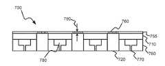
[0079]図7Bを参照すると、本発明の技術の実施形態による例示的シャワーヘッド700の断面図が示されている。シャワーヘッド700は、シャワーヘッド600にある意味で類似しており、そのシャワーヘッド、又は検討された他のシャワーヘッド若しくは面板の何れかについて検討された特徴又は特性の何れかを含み得る。シャワーヘッド700は、ポート760が板を通して形成されたチャネルの反対の端に含まれる点で、シャワーヘッド600と異なり得る。例えば、シャワーヘッド700は、第1の板710及び第2の板750を含み、連結されると、第1の板710と第2の板750との間に空間780を画定し得る。第1の板710は、通り孔720の一部を画定し、第2の板750は、通り孔720の第2の部分を画定し得る。第2の板750はまた、開孔770を画定し得る。開孔770及び通り孔720は、様々な面板及びシャワーヘッドについて先ほど検討された寸法又は特徴の何れかによって特徴付けられ得る。 [0079] Referring to FIG. 7B, a cross-sectional view of an
[0080]幾つかの実施形態では、シャワーヘッド700は、第1の板710が第2の板750に連結される表面と反対の表面で第1の板710に連結される、第3の板755によって特徴付けられ得る。他の実施形態では、第3の板755は、前述の構造に類似するカウンターボアのような構造を含む、第1の板710の一部であり得る。第3の板755は、前述のポートの特徴又は特性の何れかを含み得るポート760を画定し得る。同様に、第3の板755の厚さ790、又はポート760が内部に形成され得る第1の板の領域は、シャワーヘッド700を通してプラズマ漏出を低減又は除去するために、シャワーヘッド700にわたって改善されたRF連続性を提供しつつ、生成されたプラズマ廃水又は前駆体との相互作用を制限するために前述の厚さに類似し得る。この例示的シャワーヘッド700において、アセンブリは、ガス供給アセンブリ535同様に、チャンバ500などのチャンバに含まれ得る。シャワーヘッド700は、シャワーヘッドを通して形成されたチャネルの第1の端が処理領域560に面しているチャンバ内に位置付けられるが、チャネルの第2の端は、リッド502又は面板523に面することになり得る。 [0080] In some embodiments, the
[0081]図8Aは、本発明の技術の実施形態による例示的シャワーヘッド700の上面図を示す。図示されたように、通り孔を含む代わりに、第1の板710の一部である第3の板755は、板を通る複数の開孔760を画定し、それらは前述のポートであり得る。複数の開孔760は、第1の複数の開孔のうちの少なくとも2つの開孔を含み得る、第1の複数の群の開孔の中に画定され得る。群は、前述のような任意の数の開孔を含み得る。 [0081] FIG. 8A shows a top view of an
[0082]図8Bは、本発明の技術の実施形態による例示的シャワーヘッド700の底面図を示す。示された図は第2の板750を含み、実施形態において第1及び/又は第3の板に連結され得る。第2の板750は、複数の通り孔720を画定し、図示されたように第3の板755に画定されたポート760へのアクセスを提供し得る。各通り孔は、チャネルを生成するために第1の複数の開孔からの少なくとも1つの群の開孔と位置合わせされ得、前述の特性の何れかを含み得る。第2の板750はまた、複数の第2の開孔770を画定し、シャワーヘッドの内側空間へのアクセスを提供し得る。開孔は、前述のパターンの何れかで画定又は配置され得る。 [0082] FIG. 8B shows a bottom view of an
[0083]前述のチャンバ及びプラズマ源は、一又は複数の方法で使用され得る。図9は、本発明の技術の実施形態による例示的方法900の工程を示す。方法900は、工程905で一又は複数の前駆体をチャンバに流入させることを含み得る。チャンバは、前述のチャンバの何れかに類似し、検討されたシャワーヘッドの何れかのようなシャワーヘッドを含み得る。前駆体は、注入口アセンブリから、又は、例えば、シャワーヘッドの板の間の空間へのアクセスなど、追加のアクセスから、流され得る。前駆体は、工程910において、プラズマが内部で形成される処理領域に流入され得る。プラズマは、実施形態において、容量結合プラズマとして形成され、電極は、前述のようなシャワーヘッドだけではなく基板もその上に位置付けられるペデスタルを含み得る。形成されたプラズマは、シャワーヘッドによって少なくとも部分的に画定された処理領域内に含まれる、実質的に含まれる、又は本質的に含まれることがある。例えば、シャワーヘッドは、工程915において、プラズマ漏出がシャワーヘッドを介して制御又は除去されるように、前述のような特徴又は特性を有し得る。 [0083] The chamber and plasma source described above may be used in one or more ways. FIG. 9 illustrates steps of an
[0084]チャンバ及びシャワーヘッドはまた、チャンバの外部、又はチャンバの処理領域上流のチャンバ領域内のどちらかなど、前駆体が供給される又はプラズマ廃水が遠隔で生成される工程において使用されてもよい。例えば、プラズマ廃水は、前述のようにシャワーヘッドと面板との間で生成され得る。プラズマ廃水は、シャワーヘッドを通って画定されるチャネルを含むシャワーヘッドを通って流れ得る。チャネルは、第1の直径を有する第1の端、及び多くのポートを含む第2の端によって特徴付けられ、各ポートが第1の直径未満の直径によって特徴付けられ得る。チャネルのどちらかの端は、基板が内部に位置付けられる処理領域に近接し得る。プラズマ廃水は、チャネルを通って流れ、チャネル寸法及びポート長のため少なくとも部分的に再結合に限定的影響を与え得る。加えて、廃水は、処理領域内でエッチング及び/又は堆積を実行し、副生成物が、チャネルを通って面板まで上流を流れることが防止され得る。より大きなチャネルの端において材料の画定された厚さの範囲内のポートを含むことによって、本発明の技術のシャワーヘッドは、従来のシャワーヘッドと比較してこれらの工程の何れかにおいて改善し、シャワーヘッドのチャネルを通してプラズマ及び副生成物の漏出をもたらすことがある。 [0084] The chamber and showerhead may also be used in processes where precursors are supplied or plasma wastewater is generated remotely, such as either outside the chamber or in a chamber region upstream of the chamber processing region. Good. For example, plasma wastewater can be generated between the showerhead and faceplate as described above. Plasma wastewater may flow through the showerhead including channels defined through the showerhead. The channel may be characterized by a first end having a first diameter and a second end comprising a number of ports, each port being characterized by a diameter less than the first diameter. Either end of the channel may be proximate to the processing region in which the substrate is positioned. Plasma wastewater flows through the channel and can at least partially affect recombination due to channel size and port length. In addition, the wastewater can be etched and / or deposited in the processing area to prevent by-products from flowing upstream through the channel to the faceplate. By including a port within the defined thickness of the material at the end of the larger channel, the showerhead of the present technique improves in any of these steps compared to a conventional showerhead, Plasma and by-product leakage may occur through the showerhead channel.
[0085]上述の説明では、説明の目的のために、本発明の技術の様々な実施形態の理解を促すために、多数の詳細が記載されてきた。しかしながら、これらの詳細の幾つかを含まずに又は更なる詳細と共に、特定の実施形態を実施し得ることが、当業者には明らかであろう。 [0085] In the foregoing description, for the purposes of explanation, numerous details have been set forth in order to facilitate an understanding of various embodiments of the present technology. However, it will be apparent to one skilled in the art that certain embodiments may be practiced without some of these details or with further details.
[0086]幾つかの実施形態を開示したが、当然ながら当業者には、実施形態の主旨から逸脱することなく、様々な変更例、代替構造物、及び同等物を使用し得ることが理解されるだろう。加えて、本発明の技術を不必要に不明瞭にすることを避けるために、幾つかの周知のプロセス及び要素については説明しなかった。したがって、上記の説明は、本発明の技術の範囲を限定するものと解釈すべきではない。 [0086] While several embodiments have been disclosed, it will be appreciated by those skilled in the art that various modifications, alternative constructions, and equivalents may be used without departing from the spirit of the embodiments. It will be. In addition, some well-known processes and elements have not been described in order to avoid unnecessarily obscuring the techniques of the present invention. Therefore, the above description should not be taken as limiting the scope of the technology of the present invention.
[0087]値の範囲が付与されているところでは、文脈上そうでないと明示されていない限り、その範囲の上限値と下限値との間の各介在値は、下限値の最も小さい単位まで具体的に開示されている。記載された範囲の任意の記載値又は記載されていない介在値の間の任意の小さい範囲、そしてその記載範囲のその他任意の記載された又は介在する値も含まれる。これら小さい範囲の上限値及び下限値は、その範囲に個々に含まれ、又はその範囲から除外される場合があり、小さい範囲に限界値のいずれかが含まれる、どちらも含まれない、又は両方が含まれる各範囲もこの手法に含まれ、記載された範囲において任意に具体的に除外された限界値に依存する。記載された範囲に一又は複数の限界値が含まれるところでは、これらの含有限界値のいずれか、又は両方を除外する範囲も含まれる。 [0087] Where a range of values is given, each intervening value between the upper and lower limits of the range is specified to the smallest unit of the lower limit, unless otherwise specified in context. Have been disclosed. Also included are any stated values in the stated range or any small range between undescribed intervening values, and any other stated or intervening values in that stated range. The upper and lower limits of these small ranges may be individually included or excluded from the range, and any of the limit values may be included in the small range, neither, or both Each range that includes is also included in this approach and depends on the limit values that are arbitrarily specifically excluded in the stated range. Where one or more limit values are included in the stated range, ranges that exclude either or both of these limit values are also included.
[0088]本明細書及び特許請求の範囲で使用される単数形の「1つの(a、an)」、及び「前記(the)」は、文脈上明確な指示がない限り、複数の意味を含む。したがって、例えば、「開孔」を参照した時は複数の上記開孔を含み、「前駆体」を参照した時は、一又は複数の前駆体及び当業者に周知のそれらの同等物などへの参照を含む。 [0088] As used in the specification and claims, the singular forms "a", "an", and "the" refer to the plural meanings unless the context clearly dictates otherwise. Including. Thus, for example, reference to “aperture” includes a plurality of such apertures, and reference to “precursor” refers to one or more precursors and their equivalents well known to those skilled in the art, etc. Contains a reference.
[0089]また、「備える(comprise(s))」、「備えている(comprising)」、「含有する(contain(s))」、「含有している(containing)」、「含む(include(s))」、及び「含んでいる(including)」という単語は、本明細書及び特許請求の範囲で使用された場合、記載された特徴、整数、構成要素、又は動作の存在を特定することを意図しているが、一又は複数のその他の特徴、整数、構成要素、動作、作動、又はグループの存在、又は追加を除外するものではない。 [0089] Also, “comprise (s)”, “comprising”, “contain (s)”, “containing”, “include ( s)) ", and the word" including ", as used in the specification and claims, identify the presence of the described feature, integer, component, or action. Does not exclude the presence or addition of one or more other features, integers, components, actions, acts, or groups.
Claims (15)
Translated fromJapanese前記半導体処理チャンバの処理領域内で基板を支持するように構成されたペデスタルと、
少なくとも2つの板の間に空間を画定するために、連結された前記少なくとも2つの板を備える前記半導体処理チャンバ内に位置付けられた第1のシャワーヘッドであって、前記少なくとも2つの板が、前記第1のシャワーヘッドを通るチャネルを少なくとも部分的に画定し、各チャネルが、前記チャネルの第1の端で第1の直径によって特徴付けられ、かつ前記チャネルの第2の端で複数のポートによって特徴付けられている、第1のシャワーヘッドと
を備える半導体処理チャンバ。A chamber housing at least partially defining an interior region of the semiconductor processing chamber and comprising a lid;
A pedestal configured to support a substrate within a processing region of the semiconductor processing chamber;
A first showerhead positioned in the semiconductor processing chamber comprising the at least two plates coupled to define a space between the at least two plates, the at least two plates being the first At least partially defining channels through the showerhead, each channel characterized by a first diameter at the first end of the channel and by a plurality of ports at the second end of the channel A semiconductor processing chamber comprising a first showerhead.
前記第1の板に連結されており、第1の複数の開孔及び第2の複数の開孔を画定する第2の板であって、前記第2の複数の開孔が、前記第2の複数の開孔の少なくとも2つの開孔を含む複数の群の開孔の前記第2の板に画定され、前記第1の板の各通り孔が、チャネルを形成するために少なくとも1つの群の開孔と位置合わせされている、第2の板と
を備えるシャワーヘッド
を備えるプラズマ処理チャンバ。A first plate defining a plurality of through holes;
A second plate coupled to the first plate and defining a first plurality of apertures and a second plurality of apertures, wherein the second plurality of apertures are the second plurality of apertures; A plurality of apertures of the plurality of apertures defined in the second plate of the plurality of apertures, each through hole of the first plate being at least one group for forming a channel. A plasma processing chamber comprising a showerhead comprising a second plate aligned with the aperture of the second plate.
Priority Applications (1)
| Application Number | Priority Date | Filing Date | Title |
|---|---|---|---|
| JP2022042301AJP7355872B2 (en) | 2016-10-04 | 2022-03-17 | Dual channel shower head with improved profile |
Applications Claiming Priority (2)
| Application Number | Priority Date | Filing Date | Title |
|---|---|---|---|
| US15/285,331 | 2016-10-04 | ||
| US15/285,331US10546729B2 (en) | 2016-10-04 | 2016-10-04 | Dual-channel showerhead with improved profile |
Related Child Applications (1)
| Application Number | Title | Priority Date | Filing Date |
|---|---|---|---|
| JP2022042301ADivisionJP7355872B2 (en) | 2016-10-04 | 2022-03-17 | Dual channel shower head with improved profile |
Publications (2)
| Publication Number | Publication Date |
|---|---|
| JP2018082150Atrue JP2018082150A (en) | 2018-05-24 |
| JP7044501B2 JP7044501B2 (en) | 2022-03-30 |
Family
ID=61758340
Family Applications (2)
| Application Number | Title | Priority Date | Filing Date |
|---|---|---|---|
| JP2017171674AActiveJP7044501B2 (en) | 2016-10-04 | 2017-09-07 | Dual channel shower head with improved profile |
| JP2022042301AActiveJP7355872B2 (en) | 2016-10-04 | 2022-03-17 | Dual channel shower head with improved profile |
Family Applications After (1)
| Application Number | Title | Priority Date | Filing Date |
|---|---|---|---|
| JP2022042301AActiveJP7355872B2 (en) | 2016-10-04 | 2022-03-17 | Dual channel shower head with improved profile |
Country Status (5)
| Country | Link |
|---|---|
| US (2) | US10546729B2 (en) |
| JP (2) | JP7044501B2 (en) |
| KR (2) | KR102433298B1 (en) |
| CN (2) | CN107895683B (en) |
| TW (2) | TWI787198B (en) |
Cited By (5)
| Publication number | Priority date | Publication date | Assignee | Title |
|---|---|---|---|---|
| WO2021157374A1 (en)* | 2020-02-07 | 2021-08-12 | 東京エレクトロン株式会社 | Shower head and substrate processing device |
| WO2021216449A1 (en)* | 2020-04-23 | 2021-10-28 | Applied Materials, Inc. | Faceplate with edge flow control |
| JP2022077993A (en)* | 2020-11-12 | 2022-05-24 | ウニフェルシタイト・トゥヴェンテ | Reactor and related methods |
| JP2023535018A (en)* | 2020-07-21 | 2023-08-15 | アプライド マテリアルズ インコーポレイテッド | Distribution components for semiconductor processing systems |
| JP2024524382A (en)* | 2021-07-02 | 2024-07-05 | アプライド マテリアルズ インコーポレイテッド | Semiconductor Processing Chamber Adapter |
Families Citing this family (320)
| Publication number | Priority date | Publication date | Assignee | Title |
|---|---|---|---|---|
| US10283321B2 (en) | 2011-01-18 | 2019-05-07 | Applied Materials, Inc. | Semiconductor processing system and methods using capacitively coupled plasma |
| US20130023129A1 (en) | 2011-07-20 | 2013-01-24 | Asm America, Inc. | Pressure transmitter for a semiconductor processing environment |
| US9132436B2 (en) | 2012-09-21 | 2015-09-15 | Applied Materials, Inc. | Chemical control features in wafer process equipment |
| US20160376700A1 (en) | 2013-02-01 | 2016-12-29 | Asm Ip Holding B.V. | System for treatment of deposition reactor |
| US10256079B2 (en) | 2013-02-08 | 2019-04-09 | Applied Materials, Inc. | Semiconductor processing systems having multiple plasma configurations |
| US9362130B2 (en) | 2013-03-01 | 2016-06-07 | Applied Materials, Inc. | Enhanced etching processes using remote plasma sources |
| US9309598B2 (en) | 2014-05-28 | 2016-04-12 | Applied Materials, Inc. | Oxide and metal removal |
| US10861682B2 (en) | 2014-07-31 | 2020-12-08 | iSenseCloud, Inc. | Test wafer with optical fiber with Bragg Grating sensors |
| US10941490B2 (en) | 2014-10-07 | 2021-03-09 | Asm Ip Holding B.V. | Multiple temperature range susceptor, assembly, reactor and system including the susceptor, and methods of using the same |
| US9355922B2 (en) | 2014-10-14 | 2016-05-31 | Applied Materials, Inc. | Systems and methods for internal surface conditioning in plasma processing equipment |
| US9966240B2 (en) | 2014-10-14 | 2018-05-08 | Applied Materials, Inc. | Systems and methods for internal surface conditioning assessment in plasma processing equipment |
| US11637002B2 (en) | 2014-11-26 | 2023-04-25 | Applied Materials, Inc. | Methods and systems to enhance process uniformity |
| US10573496B2 (en) | 2014-12-09 | 2020-02-25 | Applied Materials, Inc. | Direct outlet toroidal plasma source |
| US10224210B2 (en) | 2014-12-09 | 2019-03-05 | Applied Materials, Inc. | Plasma processing system with direct outlet toroidal plasma source |
| US11257693B2 (en) | 2015-01-09 | 2022-02-22 | Applied Materials, Inc. | Methods and systems to improve pedestal temperature control |
| US9728437B2 (en) | 2015-02-03 | 2017-08-08 | Applied Materials, Inc. | High temperature chuck for plasma processing systems |
| US20160225652A1 (en) | 2015-02-03 | 2016-08-04 | Applied Materials, Inc. | Low temperature chuck for plasma processing systems |
| US10276355B2 (en) | 2015-03-12 | 2019-04-30 | Asm Ip Holding B.V. | Multi-zone reactor, system including the reactor, and method of using the same |
| US9691645B2 (en) | 2015-08-06 | 2017-06-27 | Applied Materials, Inc. | Bolted wafer chuck thermal management systems and methods for wafer processing systems |
| US9741593B2 (en) | 2015-08-06 | 2017-08-22 | Applied Materials, Inc. | Thermal management systems and methods for wafer processing systems |
| US9349605B1 (en)* | 2015-08-07 | 2016-05-24 | Applied Materials, Inc. | Oxide etch selectivity systems and methods |
| US10504700B2 (en) | 2015-08-27 | 2019-12-10 | Applied Materials, Inc. | Plasma etching systems and methods with secondary plasma injection |
| US11139308B2 (en) | 2015-12-29 | 2021-10-05 | Asm Ip Holding B.V. | Atomic layer deposition of III-V compounds to form V-NAND devices |
| US10529554B2 (en) | 2016-02-19 | 2020-01-07 | Asm Ip Holding B.V. | Method for forming silicon nitride film selectively on sidewalls or flat surfaces of trenches |
| US10343920B2 (en) | 2016-03-18 | 2019-07-09 | Asm Ip Holding B.V. | Aligned carbon nanotubes |
| US10522371B2 (en) | 2016-05-19 | 2019-12-31 | Applied Materials, Inc. | Systems and methods for improved semiconductor etching and component protection |
| US10504754B2 (en) | 2016-05-19 | 2019-12-10 | Applied Materials, Inc. | Systems and methods for improved semiconductor etching and component protection |
| US11453943B2 (en) | 2016-05-25 | 2022-09-27 | Asm Ip Holding B.V. | Method for forming carbon-containing silicon/metal oxide or nitride film by ALD using silicon precursor and hydrocarbon precursor |
| US9865484B1 (en) | 2016-06-29 | 2018-01-09 | Applied Materials, Inc. | Selective etch using material modification and RF pulsing |
| US10612137B2 (en) | 2016-07-08 | 2020-04-07 | Asm Ip Holdings B.V. | Organic reactants for atomic layer deposition |
| US9859151B1 (en) | 2016-07-08 | 2018-01-02 | Asm Ip Holding B.V. | Selective film deposition method to form air gaps |
| US9812320B1 (en) | 2016-07-28 | 2017-11-07 | Asm Ip Holding B.V. | Method and apparatus for filling a gap |
| US9887082B1 (en) | 2016-07-28 | 2018-02-06 | Asm Ip Holding B.V. | Method and apparatus for filling a gap |
| US10062575B2 (en) | 2016-09-09 | 2018-08-28 | Applied Materials, Inc. | Poly directional etch by oxidation |
| US10629473B2 (en) | 2016-09-09 | 2020-04-21 | Applied Materials, Inc. | Footing removal for nitride spacer |
| US10546729B2 (en)* | 2016-10-04 | 2020-01-28 | Applied Materials, Inc. | Dual-channel showerhead with improved profile |
| US9934942B1 (en) | 2016-10-04 | 2018-04-03 | Applied Materials, Inc. | Chamber with flow-through source |
| US10062579B2 (en) | 2016-10-07 | 2018-08-28 | Applied Materials, Inc. | Selective SiN lateral recess |
| US11532757B2 (en) | 2016-10-27 | 2022-12-20 | Asm Ip Holding B.V. | Deposition of charge trapping layers |
| US10714350B2 (en) | 2016-11-01 | 2020-07-14 | ASM IP Holdings, B.V. | Methods for forming a transition metal niobium nitride film on a substrate by atomic layer deposition and related semiconductor device structures |
| US10163696B2 (en) | 2016-11-11 | 2018-12-25 | Applied Materials, Inc. | Selective cobalt removal for bottom up gapfill |
| US9768034B1 (en) | 2016-11-11 | 2017-09-19 | Applied Materials, Inc. | Removal methods for high aspect ratio structures |
| US10242908B2 (en) | 2016-11-14 | 2019-03-26 | Applied Materials, Inc. | Airgap formation with damage-free copper |
| US10026621B2 (en) | 2016-11-14 | 2018-07-17 | Applied Materials, Inc. | SiN spacer profile patterning |
| KR102546317B1 (en) | 2016-11-15 | 2023-06-21 | 에이에스엠 아이피 홀딩 비.브이. | Gas supply unit and substrate processing apparatus including the same |
| US10604841B2 (en) | 2016-12-14 | 2020-03-31 | Lam Research Corporation | Integrated showerhead with thermal control for delivering radical and precursor gas to a downstream chamber to enable remote plasma film deposition |
| US11447861B2 (en) | 2016-12-15 | 2022-09-20 | Asm Ip Holding B.V. | Sequential infiltration synthesis apparatus and a method of forming a patterned structure |
| US11581186B2 (en) | 2016-12-15 | 2023-02-14 | Asm Ip Holding B.V. | Sequential infiltration synthesis apparatus |
| US10566206B2 (en) | 2016-12-27 | 2020-02-18 | Applied Materials, Inc. | Systems and methods for anisotropic material breakthrough |
| US11390950B2 (en) | 2017-01-10 | 2022-07-19 | Asm Ip Holding B.V. | Reactor system and method to reduce residue buildup during a film deposition process |
| US10403507B2 (en) | 2017-02-03 | 2019-09-03 | Applied Materials, Inc. | Shaped etch profile with oxidation |
| US10431429B2 (en) | 2017-02-03 | 2019-10-01 | Applied Materials, Inc. | Systems and methods for radial and azimuthal control of plasma uniformity |
| US10319739B2 (en) | 2017-02-08 | 2019-06-11 | Applied Materials, Inc. | Accommodating imperfectly aligned memory holes |
| US10468261B2 (en) | 2017-02-15 | 2019-11-05 | Asm Ip Holding B.V. | Methods for forming a metallic film on a substrate by cyclical deposition and related semiconductor device structures |
| US10943834B2 (en) | 2017-03-13 | 2021-03-09 | Applied Materials, Inc. | Replacement contact process |
| US10319649B2 (en) | 2017-04-11 | 2019-06-11 | Applied Materials, Inc. | Optical emission spectroscopy (OES) for remote plasma monitoring |
| US10770286B2 (en) | 2017-05-08 | 2020-09-08 | Asm Ip Holdings B.V. | Methods for selectively forming a silicon nitride film on a substrate and related semiconductor device structures |
| US11276590B2 (en) | 2017-05-17 | 2022-03-15 | Applied Materials, Inc. | Multi-zone semiconductor substrate supports |
| US11276559B2 (en) | 2017-05-17 | 2022-03-15 | Applied Materials, Inc. | Semiconductor processing chamber for multiple precursor flow |
| JP7176860B6 (en) | 2017-05-17 | 2022-12-16 | アプライド マテリアルズ インコーポレイテッド | Semiconductor processing chamber to improve precursor flow |
| US10497579B2 (en) | 2017-05-31 | 2019-12-03 | Applied Materials, Inc. | Water-free etching methods |
| US10049891B1 (en) | 2017-05-31 | 2018-08-14 | Applied Materials, Inc. | Selective in situ cobalt residue removal |
| US10920320B2 (en) | 2017-06-16 | 2021-02-16 | Applied Materials, Inc. | Plasma health determination in semiconductor substrate processing reactors |
| US12040200B2 (en) | 2017-06-20 | 2024-07-16 | Asm Ip Holding B.V. | Semiconductor processing apparatus and methods for calibrating a semiconductor processing apparatus |
| US10541246B2 (en) | 2017-06-26 | 2020-01-21 | Applied Materials, Inc. | 3D flash memory cells which discourage cross-cell electrical tunneling |
| US11306395B2 (en) | 2017-06-28 | 2022-04-19 | Asm Ip Holding B.V. | Methods for depositing a transition metal nitride film on a substrate by atomic layer deposition and related deposition apparatus |
| US10727080B2 (en) | 2017-07-07 | 2020-07-28 | Applied Materials, Inc. | Tantalum-containing material removal |
| US10541184B2 (en) | 2017-07-11 | 2020-01-21 | Applied Materials, Inc. | Optical emission spectroscopic techniques for monitoring etching |
| US10354889B2 (en) | 2017-07-17 | 2019-07-16 | Applied Materials, Inc. | Non-halogen etching of silicon-containing materials |
| KR20190009245A (en) | 2017-07-18 | 2019-01-28 | 에이에스엠 아이피 홀딩 비.브이. | Methods for forming a semiconductor device structure and related semiconductor device structures |
| US11374112B2 (en) | 2017-07-19 | 2022-06-28 | Asm Ip Holding B.V. | Method for depositing a group IV semiconductor and related semiconductor device structures |
| US10590535B2 (en) | 2017-07-26 | 2020-03-17 | Asm Ip Holdings B.V. | Chemical treatment, deposition and/or infiltration apparatus and method for using the same |
| US10043674B1 (en) | 2017-08-04 | 2018-08-07 | Applied Materials, Inc. | Germanium etching systems and methods |
| US10170336B1 (en) | 2017-08-04 | 2019-01-01 | Applied Materials, Inc. | Methods for anisotropic control of selective silicon removal |
| TWI815813B (en) | 2017-08-04 | 2023-09-21 | 荷蘭商Asm智慧財產控股公司 | Showerhead assembly for distributing a gas within a reaction chamber |
| US10297458B2 (en) | 2017-08-07 | 2019-05-21 | Applied Materials, Inc. | Process window widening using coated parts in plasma etch processes |
| US10770336B2 (en) | 2017-08-08 | 2020-09-08 | Asm Ip Holding B.V. | Substrate lift mechanism and reactor including same |
| US10692741B2 (en) | 2017-08-08 | 2020-06-23 | Asm Ip Holdings B.V. | Radiation shield |
| US11769682B2 (en) | 2017-08-09 | 2023-09-26 | Asm Ip Holding B.V. | Storage apparatus for storing cassettes for substrates and processing apparatus equipped therewith |
| US11830730B2 (en) | 2017-08-29 | 2023-11-28 | Asm Ip Holding B.V. | Layer forming method and apparatus |
| US11295980B2 (en) | 2017-08-30 | 2022-04-05 | Asm Ip Holding B.V. | Methods for depositing a molybdenum metal film over a dielectric surface of a substrate by a cyclical deposition process and related semiconductor device structures |
| US10658205B2 (en) | 2017-09-28 | 2020-05-19 | Asm Ip Holdings B.V. | Chemical dispensing apparatus and methods for dispensing a chemical to a reaction chamber |
| US10403504B2 (en) | 2017-10-05 | 2019-09-03 | Asm Ip Holding B.V. | Method for selectively depositing a metallic film on a substrate |
| US10283324B1 (en) | 2017-10-24 | 2019-05-07 | Applied Materials, Inc. | Oxygen treatment for nitride etching |
| US10128086B1 (en) | 2017-10-24 | 2018-11-13 | Applied Materials, Inc. | Silicon pretreatment for nitride removal |
| US10424487B2 (en) | 2017-10-24 | 2019-09-24 | Applied Materials, Inc. | Atomic layer etching processes |
| US10923344B2 (en) | 2017-10-30 | 2021-02-16 | Asm Ip Holding B.V. | Methods for forming a semiconductor structure and related semiconductor structures |
| WO2019103613A1 (en) | 2017-11-27 | 2019-05-31 | Asm Ip Holding B.V. | A storage device for storing wafer cassettes for use with a batch furnace |
| CN111344522B (en) | 2017-11-27 | 2022-04-12 | 阿斯莫Ip控股公司 | Including clean mini-environment device |
| US10256112B1 (en) | 2017-12-08 | 2019-04-09 | Applied Materials, Inc. | Selective tungsten removal |
| WO2019113478A1 (en)* | 2017-12-08 | 2019-06-13 | Lam Research Corporation | Integrated showerhead with improved hole pattern for delivering radical and precursor gas to a downstream chamber to enable remote plasma film deposition |
| US10903054B2 (en) | 2017-12-19 | 2021-01-26 | Applied Materials, Inc. | Multi-zone gas distribution systems and methods |
| US11328909B2 (en) | 2017-12-22 | 2022-05-10 | Applied Materials, Inc. | Chamber conditioning and removal processes |
| US10854426B2 (en) | 2018-01-08 | 2020-12-01 | Applied Materials, Inc. | Metal recess for semiconductor structures |
| US11149350B2 (en)* | 2018-01-10 | 2021-10-19 | Asm Ip Holding B.V. | Shower plate structure for supplying carrier and dry gas |
| US10872771B2 (en) | 2018-01-16 | 2020-12-22 | Asm Ip Holding B. V. | Method for depositing a material film on a substrate within a reaction chamber by a cyclical deposition process and related device structures |
| KR102695659B1 (en) | 2018-01-19 | 2024-08-14 | 에이에스엠 아이피 홀딩 비.브이. | Method for depositing a gap filling layer by plasma assisted deposition |
| TWI799494B (en) | 2018-01-19 | 2023-04-21 | 荷蘭商Asm 智慧財產控股公司 | Deposition method |
| US11081345B2 (en) | 2018-02-06 | 2021-08-03 | Asm Ip Holding B.V. | Method of post-deposition treatment for silicon oxide film |
| US10896820B2 (en) | 2018-02-14 | 2021-01-19 | Asm Ip Holding B.V. | Method for depositing a ruthenium-containing film on a substrate by a cyclical deposition process |
| WO2019158960A1 (en) | 2018-02-14 | 2019-08-22 | Asm Ip Holding B.V. | A method for depositing a ruthenium-containing film on a substrate by a cyclical deposition process |
| US10964512B2 (en) | 2018-02-15 | 2021-03-30 | Applied Materials, Inc. | Semiconductor processing chamber multistage mixing apparatus and methods |
| US10679870B2 (en) | 2018-02-15 | 2020-06-09 | Applied Materials, Inc. | Semiconductor processing chamber multistage mixing apparatus |
| US10731249B2 (en) | 2018-02-15 | 2020-08-04 | Asm Ip Holding B.V. | Method of forming a transition metal containing film on a substrate by a cyclical deposition process, a method for supplying a transition metal halide compound to a reaction chamber, and related vapor deposition apparatus |
| KR102636427B1 (en) | 2018-02-20 | 2024-02-13 | 에이에스엠 아이피 홀딩 비.브이. | Substrate processing method and apparatus |
| US10975470B2 (en) | 2018-02-23 | 2021-04-13 | Asm Ip Holding B.V. | Apparatus for detecting or monitoring for a chemical precursor in a high temperature environment |
| TWI766433B (en) | 2018-02-28 | 2022-06-01 | 美商應用材料股份有限公司 | Systems and methods to form airgaps |
| US11473195B2 (en) | 2018-03-01 | 2022-10-18 | Asm Ip Holding B.V. | Semiconductor processing apparatus and a method for processing a substrate |
| US10593560B2 (en) | 2018-03-01 | 2020-03-17 | Applied Materials, Inc. | Magnetic induction plasma source for semiconductor processes and equipment |
| US10319600B1 (en) | 2018-03-12 | 2019-06-11 | Applied Materials, Inc. | Thermal silicon etch |
| US10497573B2 (en) | 2018-03-13 | 2019-12-03 | Applied Materials, Inc. | Selective atomic layer etching of semiconductor materials |
| KR102646467B1 (en) | 2018-03-27 | 2024-03-11 | 에이에스엠 아이피 홀딩 비.브이. | Method of forming an electrode on a substrate and a semiconductor device structure including an electrode |
| US10573527B2 (en) | 2018-04-06 | 2020-02-25 | Applied Materials, Inc. | Gas-phase selective etching systems and methods |
| KR102600229B1 (en) | 2018-04-09 | 2023-11-10 | 에이에스엠 아이피 홀딩 비.브이. | Substrate supporting device, substrate processing apparatus including the same and substrate processing method |
| US10490406B2 (en) | 2018-04-10 | 2019-11-26 | Appled Materials, Inc. | Systems and methods for material breakthrough |
| US10699879B2 (en) | 2018-04-17 | 2020-06-30 | Applied Materials, Inc. | Two piece electrode assembly with gap for plasma control |
| US10886137B2 (en) | 2018-04-30 | 2021-01-05 | Applied Materials, Inc. | Selective nitride removal |
| US12025484B2 (en) | 2018-05-08 | 2024-07-02 | Asm Ip Holding B.V. | Thin film forming method |
| US12272527B2 (en) | 2018-05-09 | 2025-04-08 | Asm Ip Holding B.V. | Apparatus for use with hydrogen radicals and method of using same |
| KR102596988B1 (en) | 2018-05-28 | 2023-10-31 | 에이에스엠 아이피 홀딩 비.브이. | Method of processing a substrate and a device manufactured by the same |
| US11718913B2 (en) | 2018-06-04 | 2023-08-08 | Asm Ip Holding B.V. | Gas distribution system and reactor system including same |
| KR102568797B1 (en) | 2018-06-21 | 2023-08-21 | 에이에스엠 아이피 홀딩 비.브이. | Substrate processing system |
| US10797133B2 (en) | 2018-06-21 | 2020-10-06 | Asm Ip Holding B.V. | Method for depositing a phosphorus doped silicon arsenide film and related semiconductor device structures |
| TWI873894B (en) | 2018-06-27 | 2025-02-21 | 荷蘭商Asm Ip私人控股有限公司 | Cyclic deposition methods for forming metal-containing material and films and structures including the metal-containing material |
| KR102854019B1 (en) | 2018-06-27 | 2025-09-02 | 에이에스엠 아이피 홀딩 비.브이. | Periodic deposition method for forming a metal-containing material and films and structures comprising the metal-containing material |
| US10388513B1 (en) | 2018-07-03 | 2019-08-20 | Asm Ip Holding B.V. | Method for depositing silicon-free carbon-containing film as gap-fill layer by pulse plasma-assisted deposition |
| US10755922B2 (en) | 2018-07-03 | 2020-08-25 | Asm Ip Holding B.V. | Method for depositing silicon-free carbon-containing film as gap-fill layer by pulse plasma-assisted deposition |
| US10872778B2 (en) | 2018-07-06 | 2020-12-22 | Applied Materials, Inc. | Systems and methods utilizing solid-phase etchants |
| US10755941B2 (en) | 2018-07-06 | 2020-08-25 | Applied Materials, Inc. | Self-limiting selective etching systems and methods |
| US10672642B2 (en) | 2018-07-24 | 2020-06-02 | Applied Materials, Inc. | Systems and methods for pedestal configuration |
| US11430674B2 (en) | 2018-08-22 | 2022-08-30 | Asm Ip Holding B.V. | Sensor array, apparatus for dispensing a vapor phase reactant to a reaction chamber and related methods |
| KR102707956B1 (en) | 2018-09-11 | 2024-09-19 | 에이에스엠 아이피 홀딩 비.브이. | Method for deposition of a thin film |
| US11024523B2 (en) | 2018-09-11 | 2021-06-01 | Asm Ip Holding B.V. | Substrate processing apparatus and method |
| US10892198B2 (en) | 2018-09-14 | 2021-01-12 | Applied Materials, Inc. | Systems and methods for improved performance in semiconductor processing |
| US11049755B2 (en) | 2018-09-14 | 2021-06-29 | Applied Materials, Inc. | Semiconductor substrate supports with embedded RF shield |
| US11062887B2 (en) | 2018-09-17 | 2021-07-13 | Applied Materials, Inc. | High temperature RF heater pedestals |
| US11417534B2 (en) | 2018-09-21 | 2022-08-16 | Applied Materials, Inc. | Selective material removal |
| CN110970344B (en) | 2018-10-01 | 2024-10-25 | Asmip控股有限公司 | Substrate holding apparatus, system comprising the same and method of using the same |
| KR102592699B1 (en) | 2018-10-08 | 2023-10-23 | 에이에스엠 아이피 홀딩 비.브이. | Substrate support unit and apparatuses for depositing thin film and processing the substrate including the same |
| US11682560B2 (en) | 2018-10-11 | 2023-06-20 | Applied Materials, Inc. | Systems and methods for hafnium-containing film removal |
| KR102546322B1 (en) | 2018-10-19 | 2023-06-21 | 에이에스엠 아이피 홀딩 비.브이. | Substrate processing apparatus and substrate processing method |
| US11121002B2 (en) | 2018-10-24 | 2021-09-14 | Applied Materials, Inc. | Systems and methods for etching metals and metal derivatives |
| US12378665B2 (en) | 2018-10-26 | 2025-08-05 | Asm Ip Holding B.V. | High temperature coatings for a preclean and etch apparatus and related methods |
| US11087997B2 (en) | 2018-10-31 | 2021-08-10 | Asm Ip Holding B.V. | Substrate processing apparatus for processing substrates |
| KR102748291B1 (en) | 2018-11-02 | 2024-12-31 | 에이에스엠 아이피 홀딩 비.브이. | Substrate support unit and substrate processing apparatus including the same |
| US11572620B2 (en) | 2018-11-06 | 2023-02-07 | Asm Ip Holding B.V. | Methods for selectively depositing an amorphous silicon film on a substrate |
| US10818758B2 (en) | 2018-11-16 | 2020-10-27 | Asm Ip Holding B.V. | Methods for forming a metal silicate film on a substrate in a reaction chamber and related semiconductor device structures |
| US11437242B2 (en) | 2018-11-27 | 2022-09-06 | Applied Materials, Inc. | Selective removal of silicon-containing materials |
| US12040199B2 (en) | 2018-11-28 | 2024-07-16 | Asm Ip Holding B.V. | Substrate processing apparatus for processing substrates |
| KR102636428B1 (en) | 2018-12-04 | 2024-02-13 | 에이에스엠 아이피 홀딩 비.브이. | A method for cleaning a substrate processing apparatus |
| US11158513B2 (en) | 2018-12-13 | 2021-10-26 | Asm Ip Holding B.V. | Methods for forming a rhenium-containing film on a substrate by a cyclical deposition process and related semiconductor device structures |
| CN111321391A (en)* | 2018-12-13 | 2020-06-23 | 夏泰鑫半导体(青岛)有限公司 | Spray head for semiconductor manufacturing |
| TWI874340B (en) | 2018-12-14 | 2025-03-01 | 荷蘭商Asm Ip私人控股有限公司 | Method of forming device structure, structure formed by the method and system for performing the method |
| US11721527B2 (en) | 2019-01-07 | 2023-08-08 | Applied Materials, Inc. | Processing chamber mixing systems |
| US10920319B2 (en) | 2019-01-11 | 2021-02-16 | Applied Materials, Inc. | Ceramic showerheads with conductive electrodes |
| TWI866480B (en) | 2019-01-17 | 2024-12-11 | 荷蘭商Asm Ip 私人控股有限公司 | Methods of forming a transition metal containing film on a substrate by a cyclical deposition process |
| SG11202108332VA (en)* | 2019-02-01 | 2021-08-30 | Lam Res Corp | Showerhead for deposition tools having multiple plenums and gas distribution chambers |
| TWI873122B (en) | 2019-02-20 | 2025-02-21 | 荷蘭商Asm Ip私人控股有限公司 | Method of filling a recess formed within a surface of a substrate, semiconductor structure formed according to the method, and semiconductor processing apparatus |
| TWI838458B (en) | 2019-02-20 | 2024-04-11 | 荷蘭商Asm Ip私人控股有限公司 | Apparatus and methods for plug fill deposition in 3-d nand applications |
| TWI845607B (en) | 2019-02-20 | 2024-06-21 | 荷蘭商Asm Ip私人控股有限公司 | Cyclical deposition method and apparatus for filling a recess formed within a substrate surface |
| TWI842826B (en) | 2019-02-22 | 2024-05-21 | 荷蘭商Asm Ip私人控股有限公司 | Substrate processing apparatus and method for processing substrate |
| KR102858005B1 (en) | 2019-03-08 | 2025-09-09 | 에이에스엠 아이피 홀딩 비.브이. | Method for Selective Deposition of Silicon Nitride Layer and Structure Including Selectively-Deposited Silicon Nitride Layer |
| US11742198B2 (en) | 2019-03-08 | 2023-08-29 | Asm Ip Holding B.V. | Structure including SiOCN layer and method of forming same |
| JP2020167398A (en) | 2019-03-28 | 2020-10-08 | エーエスエム・アイピー・ホールディング・ベー・フェー | Door openers and substrate processing equipment provided with door openers |
| KR102809999B1 (en) | 2019-04-01 | 2025-05-19 | 에이에스엠 아이피 홀딩 비.브이. | Method of manufacturing semiconductor device |
| KR20200123380A (en) | 2019-04-19 | 2020-10-29 | 에이에스엠 아이피 홀딩 비.브이. | Layer forming method and apparatus |
| KR20200125453A (en) | 2019-04-24 | 2020-11-04 | 에이에스엠 아이피 홀딩 비.브이. | Gas-phase reactor system and method of using same |
| KR20200130121A (en) | 2019-05-07 | 2020-11-18 | 에이에스엠 아이피 홀딩 비.브이. | Chemical source vessel with dip tube |
| KR20200130652A (en) | 2019-05-10 | 2020-11-19 | 에이에스엠 아이피 홀딩 비.브이. | Method of depositing material onto a surface and structure formed according to the method |
| JP7612342B2 (en) | 2019-05-16 | 2025-01-14 | エーエスエム・アイピー・ホールディング・ベー・フェー | Wafer boat handling apparatus, vertical batch furnace and method |
| JP7598201B2 (en) | 2019-05-16 | 2024-12-11 | エーエスエム・アイピー・ホールディング・ベー・フェー | Wafer boat handling apparatus, vertical batch furnace and method |
| USD947913S1 (en) | 2019-05-17 | 2022-04-05 | Asm Ip Holding B.V. | Susceptor shaft |
| USD975665S1 (en) | 2019-05-17 | 2023-01-17 | Asm Ip Holding B.V. | Susceptor shaft |
| KR20200141002A (en) | 2019-06-06 | 2020-12-17 | 에이에스엠 아이피 홀딩 비.브이. | Method of using a gas-phase reactor system including analyzing exhausted gas |
| KR20200141931A (en) | 2019-06-10 | 2020-12-21 | 에이에스엠 아이피 홀딩 비.브이. | Method for cleaning quartz epitaxial chambers |
| KR20200143254A (en) | 2019-06-11 | 2020-12-23 | 에이에스엠 아이피 홀딩 비.브이. | Method of forming an electronic structure using an reforming gas, system for performing the method, and structure formed using the method |
| USD944946S1 (en)* | 2019-06-14 | 2022-03-01 | Asm Ip Holding B.V. | Shower plate |
| KR20210005515A (en) | 2019-07-03 | 2021-01-14 | 에이에스엠 아이피 홀딩 비.브이. | Temperature control assembly for substrate processing apparatus and method of using same |
| JP7499079B2 (en) | 2019-07-09 | 2024-06-13 | エーエスエム・アイピー・ホールディング・ベー・フェー | Plasma device using coaxial waveguide and substrate processing method |
| CN112216646A (en) | 2019-07-10 | 2021-01-12 | Asm Ip私人控股有限公司 | Substrate supporting assembly and substrate processing device comprising same |
| KR20210010307A (en) | 2019-07-16 | 2021-01-27 | 에이에스엠 아이피 홀딩 비.브이. | Substrate processing apparatus |
| KR102860110B1 (en) | 2019-07-17 | 2025-09-16 | 에이에스엠 아이피 홀딩 비.브이. | Methods of forming silicon germanium structures |
| KR20210010816A (en) | 2019-07-17 | 2021-01-28 | 에이에스엠 아이피 홀딩 비.브이. | Radical assist ignition plasma system and method |
| KR102409660B1 (en) | 2019-07-18 | 2022-06-22 | 주식회사 히타치하이테크 | plasma processing unit |
| US11643724B2 (en) | 2019-07-18 | 2023-05-09 | Asm Ip Holding B.V. | Method of forming structures using a neutral beam |
| KR20210010817A (en) | 2019-07-19 | 2021-01-28 | 에이에스엠 아이피 홀딩 비.브이. | Method of Forming Topology-Controlled Amorphous Carbon Polymer Film |
| TWI851767B (en) | 2019-07-29 | 2024-08-11 | 荷蘭商Asm Ip私人控股有限公司 | Methods for selective deposition utilizing n-type dopants and/or alternative dopants to achieve high dopant incorporation |
| CN112309900A (en) | 2019-07-30 | 2021-02-02 | Asm Ip私人控股有限公司 | Substrate processing apparatus |
| CN112309899A (en) | 2019-07-30 | 2021-02-02 | Asm Ip私人控股有限公司 | Substrate processing apparatus |
| US12169361B2 (en) | 2019-07-30 | 2024-12-17 | Asm Ip Holding B.V. | Substrate processing apparatus and method |
| US11587815B2 (en) | 2019-07-31 | 2023-02-21 | Asm Ip Holding B.V. | Vertical batch furnace assembly |
| US11227782B2 (en) | 2019-07-31 | 2022-01-18 | Asm Ip Holding B.V. | Vertical batch furnace assembly |
| US11587814B2 (en) | 2019-07-31 | 2023-02-21 | Asm Ip Holding B.V. | Vertical batch furnace assembly |
| CN112323048B (en) | 2019-08-05 | 2024-02-09 | Asm Ip私人控股有限公司 | Liquid level sensor for chemical source container |
| CN112342526A (en) | 2019-08-09 | 2021-02-09 | Asm Ip私人控股有限公司 | Heater assembly including cooling device and method of using same |
| USD965044S1 (en) | 2019-08-19 | 2022-09-27 | Asm Ip Holding B.V. | Susceptor shaft |
| USD965524S1 (en) | 2019-08-19 | 2022-10-04 | Asm Ip Holding B.V. | Susceptor support |
| JP2021031769A (en) | 2019-08-21 | 2021-03-01 | エーエスエム アイピー ホールディング ビー.ブイ. | Production apparatus of mixed gas of film deposition raw material and film deposition apparatus |
| USD979506S1 (en) | 2019-08-22 | 2023-02-28 | Asm Ip Holding B.V. | Insulator |
| KR20210024423A (en) | 2019-08-22 | 2021-03-05 | 에이에스엠 아이피 홀딩 비.브이. | Method for forming a structure with a hole |
| US11286558B2 (en) | 2019-08-23 | 2022-03-29 | Asm Ip Holding B.V. | Methods for depositing a molybdenum nitride film on a surface of a substrate by a cyclical deposition process and related semiconductor device structures including a molybdenum nitride film |
| KR20210024420A (en) | 2019-08-23 | 2021-03-05 | 에이에스엠 아이피 홀딩 비.브이. | Method for depositing silicon oxide film having improved quality by peald using bis(diethylamino)silane |
| KR102806450B1 (en) | 2019-09-04 | 2025-05-12 | 에이에스엠 아이피 홀딩 비.브이. | Methods for selective deposition using a sacrificial capping layer |
| KR102733104B1 (en) | 2019-09-05 | 2024-11-22 | 에이에스엠 아이피 홀딩 비.브이. | Substrate processing apparatus |
| WO2021050308A1 (en)* | 2019-09-12 | 2021-03-18 | Applied Materials, Inc. | Repulsion mesh and deposition methods |
| US11562901B2 (en) | 2019-09-25 | 2023-01-24 | Asm Ip Holding B.V. | Substrate processing method |
| CN112593212B (en) | 2019-10-02 | 2023-12-22 | Asm Ip私人控股有限公司 | Method for forming topologically selective silicon oxide film by cyclic plasma enhanced deposition process |
| KR20210042810A (en) | 2019-10-08 | 2021-04-20 | 에이에스엠 아이피 홀딩 비.브이. | Reactor system including a gas distribution assembly for use with activated species and method of using same |
| TWI846953B (en) | 2019-10-08 | 2024-07-01 | 荷蘭商Asm Ip私人控股有限公司 | Substrate processing device |
| TW202128273A (en) | 2019-10-08 | 2021-08-01 | 荷蘭商Asm Ip私人控股有限公司 | Gas injection system, reactor system, and method of depositing material on surface of substratewithin reaction chamber |
| TWI846966B (en) | 2019-10-10 | 2024-07-01 | 荷蘭商Asm Ip私人控股有限公司 | Method of forming a photoresist underlayer and structure including same |
| US12009241B2 (en) | 2019-10-14 | 2024-06-11 | Asm Ip Holding B.V. | Vertical batch furnace assembly with detector to detect cassette |
| TWI834919B (en) | 2019-10-16 | 2024-03-11 | 荷蘭商Asm Ip私人控股有限公司 | Method of topology-selective film formation of silicon oxide |
| US11637014B2 (en) | 2019-10-17 | 2023-04-25 | Asm Ip Holding B.V. | Methods for selective deposition of doped semiconductor material |
| KR102845724B1 (en) | 2019-10-21 | 2025-08-13 | 에이에스엠 아이피 홀딩 비.브이. | Apparatus and methods for selectively etching films |
| KR20210050453A (en) | 2019-10-25 | 2021-05-07 | 에이에스엠 아이피 홀딩 비.브이. | Methods for filling a gap feature on a substrate surface and related semiconductor structures |
| US11646205B2 (en) | 2019-10-29 | 2023-05-09 | Asm Ip Holding B.V. | Methods of selectively forming n-type doped material on a surface, systems for selectively forming n-type doped material, and structures formed using same |
| US11555244B2 (en) | 2019-11-05 | 2023-01-17 | Applied Materials, Inc. | High temperature dual chamber showerhead |
| KR20210054983A (en) | 2019-11-05 | 2021-05-14 | 에이에스엠 아이피 홀딩 비.브이. | Structures with doped semiconductor layers and methods and systems for forming same |
| US11501968B2 (en) | 2019-11-15 | 2022-11-15 | Asm Ip Holding B.V. | Method for providing a semiconductor device with silicon filled gaps |
| KR102861314B1 (en) | 2019-11-20 | 2025-09-17 | 에이에스엠 아이피 홀딩 비.브이. | Method of depositing carbon-containing material on a surface of a substrate, structure formed using the method, and system for forming the structure |
| CN112951697B (en) | 2019-11-26 | 2025-07-29 | Asmip私人控股有限公司 | Substrate processing apparatus |
| US11450529B2 (en) | 2019-11-26 | 2022-09-20 | Asm Ip Holding B.V. | Methods for selectively forming a target film on a substrate comprising a first dielectric surface and a second metallic surface |
| CN120432376A (en) | 2019-11-29 | 2025-08-05 | Asm Ip私人控股有限公司 | Substrate processing apparatus |
| CN112885692B (en) | 2019-11-29 | 2025-08-15 | Asmip私人控股有限公司 | Substrate processing apparatus |
| JP7527928B2 (en) | 2019-12-02 | 2024-08-05 | エーエスエム・アイピー・ホールディング・ベー・フェー | Substrate processing apparatus and substrate processing method |
| KR20210070898A (en) | 2019-12-04 | 2021-06-15 | 에이에스엠 아이피 홀딩 비.브이. | Substrate processing apparatus |
| KR20210078405A (en) | 2019-12-17 | 2021-06-28 | 에이에스엠 아이피 홀딩 비.브이. | Method of forming vanadium nitride layer and structure including the vanadium nitride layer |
| KR20210080214A (en) | 2019-12-19 | 2021-06-30 | 에이에스엠 아이피 홀딩 비.브이. | Methods for filling a gap feature on a substrate and related semiconductor structures |
| JP7730637B2 (en) | 2020-01-06 | 2025-08-28 | エーエスエム・アイピー・ホールディング・ベー・フェー | Gas delivery assembly, components thereof, and reactor system including same |
| JP7636892B2 (en) | 2020-01-06 | 2025-02-27 | エーエスエム・アイピー・ホールディング・ベー・フェー | Channeled Lift Pins |
| US11993847B2 (en) | 2020-01-08 | 2024-05-28 | Asm Ip Holding B.V. | Injector |
| KR20210093163A (en) | 2020-01-16 | 2021-07-27 | 에이에스엠 아이피 홀딩 비.브이. | Method of forming high aspect ratio features |
| CN111161993A (en)* | 2020-01-19 | 2020-05-15 | 无锡市邑勉微电子有限公司 | Faraday shielding reaction chamber |
| KR102675856B1 (en) | 2020-01-20 | 2024-06-17 | 에이에스엠 아이피 홀딩 비.브이. | Method of forming thin film and method of modifying surface of thin film |
| TWI889744B (en) | 2020-01-29 | 2025-07-11 | 荷蘭商Asm Ip私人控股有限公司 | Contaminant trap system, and baffle plate stack |
| TW202513845A (en) | 2020-02-03 | 2025-04-01 | 荷蘭商Asm Ip私人控股有限公司 | Semiconductor structures and methods for forming the same |
| KR20210100010A (en) | 2020-02-04 | 2021-08-13 | 에이에스엠 아이피 홀딩 비.브이. | Method and apparatus for transmittance measurements of large articles |
| US11776846B2 (en) | 2020-02-07 | 2023-10-03 | Asm Ip Holding B.V. | Methods for depositing gap filling fluids and related systems and devices |
| TW202146691A (en) | 2020-02-13 | 2021-12-16 | 荷蘭商Asm Ip私人控股有限公司 | Gas distribution assembly, shower plate assembly, and method of adjusting conductance of gas to reaction chamber |
| KR20210103956A (en) | 2020-02-13 | 2021-08-24 | 에이에스엠 아이피 홀딩 비.브이. | Substrate processing apparatus including light receiving device and calibration method of light receiving device |
| TWI855223B (en) | 2020-02-17 | 2024-09-11 | 荷蘭商Asm Ip私人控股有限公司 | Method for growing phosphorous-doped silicon layer |
| CN113410160A (en) | 2020-02-28 | 2021-09-17 | Asm Ip私人控股有限公司 | System specially used for cleaning parts |
| KR20210113043A (en) | 2020-03-04 | 2021-09-15 | 에이에스엠 아이피 홀딩 비.브이. | Alignment fixture for a reactor system |
| KR20210116240A (en) | 2020-03-11 | 2021-09-27 | 에이에스엠 아이피 홀딩 비.브이. | Substrate handling device with adjustable joints |
| US11876356B2 (en) | 2020-03-11 | 2024-01-16 | Asm Ip Holding B.V. | Lockout tagout assembly and system and method of using same |
| KR102775390B1 (en) | 2020-03-12 | 2025-02-28 | 에이에스엠 아이피 홀딩 비.브이. | Method for Fabricating Layer Structure Having Target Topological Profile |
| US12173404B2 (en) | 2020-03-17 | 2024-12-24 | Asm Ip Holding B.V. | Method of depositing epitaxial material, structure formed using the method, and system for performing the method |
| KR102755229B1 (en) | 2020-04-02 | 2025-01-14 | 에이에스엠 아이피 홀딩 비.브이. | Thin film forming method |
| TWI887376B (en) | 2020-04-03 | 2025-06-21 | 荷蘭商Asm Ip私人控股有限公司 | Method for manufacturing semiconductor device |
| TWI888525B (en) | 2020-04-08 | 2025-07-01 | 荷蘭商Asm Ip私人控股有限公司 | Apparatus and methods for selectively etching silcon oxide films |
| KR20210127620A (en) | 2020-04-13 | 2021-10-22 | 에이에스엠 아이피 홀딩 비.브이. | method of forming a nitrogen-containing carbon film and system for performing the method |
| KR20210128343A (en) | 2020-04-15 | 2021-10-26 | 에이에스엠 아이피 홀딩 비.브이. | Method of forming chromium nitride layer and structure including the chromium nitride layer |
| US11821078B2 (en) | 2020-04-15 | 2023-11-21 | Asm Ip Holding B.V. | Method for forming precoat film and method for forming silicon-containing film |
| US11996289B2 (en) | 2020-04-16 | 2024-05-28 | Asm Ip Holding B.V. | Methods of forming structures including silicon germanium and silicon layers, devices formed using the methods, and systems for performing the methods |
| KR20210130646A (en) | 2020-04-21 | 2021-11-01 | 에이에스엠 아이피 홀딩 비.브이. | Method for processing a substrate |
| TW202208671A (en) | 2020-04-24 | 2022-03-01 | 荷蘭商Asm Ip私人控股有限公司 | Methods of forming structures including vanadium boride and vanadium phosphide layers |
| KR20210132612A (en) | 2020-04-24 | 2021-11-04 | 에이에스엠 아이피 홀딩 비.브이. | Methods and apparatus for stabilizing vanadium compounds |
| KR102866804B1 (en) | 2020-04-24 | 2025-09-30 | 에이에스엠 아이피 홀딩 비.브이. | Vertical batch furnace assembly comprising a cooling gas supply |
| CN113555279A (en) | 2020-04-24 | 2021-10-26 | Asm Ip私人控股有限公司 | Methods of forming vanadium nitride-containing layers and structures comprising the same |
| KR20210132600A (en) | 2020-04-24 | 2021-11-04 | 에이에스엠 아이피 홀딩 비.브이. | Methods and systems for depositing a layer comprising vanadium, nitrogen, and a further element |
| KR102783898B1 (en) | 2020-04-29 | 2025-03-18 | 에이에스엠 아이피 홀딩 비.브이. | Solid source precursor vessel |
| KR20210134869A (en) | 2020-05-01 | 2021-11-11 | 에이에스엠 아이피 홀딩 비.브이. | Fast FOUP swapping with a FOUP handler |
| JP7726664B2 (en) | 2020-05-04 | 2025-08-20 | エーエスエム・アイピー・ホールディング・ベー・フェー | Substrate processing system for processing a substrate |
| KR20210137395A (en) | 2020-05-07 | 2021-11-17 | 에이에스엠 아이피 홀딩 비.브이. | Apparatus and methods for performing an in-situ etch of reaction chambers with fluorine-based radicals |
| CN111501024A (en)* | 2020-05-08 | 2020-08-07 | Tcl华星光电技术有限公司 | Vapor deposition apparatus |
| KR102788543B1 (en) | 2020-05-13 | 2025-03-27 | 에이에스엠 아이피 홀딩 비.브이. | Laser alignment fixture for a reactor system |
| TW202146699A (en) | 2020-05-15 | 2021-12-16 | 荷蘭商Asm Ip私人控股有限公司 | Method of forming a silicon germanium layer, semiconductor structure, semiconductor device, method of forming a deposition layer, and deposition system |
| KR20210143653A (en) | 2020-05-19 | 2021-11-29 | 에이에스엠 아이피 홀딩 비.브이. | Substrate processing apparatus |
| KR20210145079A (en) | 2020-05-21 | 2021-12-01 | 에이에스엠 아이피 홀딩 비.브이. | Flange and apparatus for processing substrates |
| KR102795476B1 (en) | 2020-05-21 | 2025-04-11 | 에이에스엠 아이피 홀딩 비.브이. | Structures including multiple carbon layers and methods of forming and using same |
| TWI873343B (en) | 2020-05-22 | 2025-02-21 | 荷蘭商Asm Ip私人控股有限公司 | Reaction system for forming thin film on substrate |
| KR20210146802A (en) | 2020-05-26 | 2021-12-06 | 에이에스엠 아이피 홀딩 비.브이. | Method for depositing boron and gallium containing silicon germanium layers |
| TWI876048B (en) | 2020-05-29 | 2025-03-11 | 荷蘭商Asm Ip私人控股有限公司 | Substrate processing device |
| TW202212620A (en) | 2020-06-02 | 2022-04-01 | 荷蘭商Asm Ip私人控股有限公司 | Apparatus for processing substrate, method of forming film, and method of controlling apparatus for processing substrate |
| TW202208659A (en) | 2020-06-16 | 2022-03-01 | 荷蘭商Asm Ip私人控股有限公司 | Method for depositing boron containing silicon germanium layers |
| TW202218133A (en) | 2020-06-24 | 2022-05-01 | 荷蘭商Asm Ip私人控股有限公司 | Method for forming a layer provided with silicon |
| TWI873359B (en) | 2020-06-30 | 2025-02-21 | 荷蘭商Asm Ip私人控股有限公司 | Substrate processing method |
| TW202202649A (en) | 2020-07-08 | 2022-01-16 | 荷蘭商Asm Ip私人控股有限公司 | Substrate processing method |
| KR20220010438A (en) | 2020-07-17 | 2022-01-25 | 에이에스엠 아이피 홀딩 비.브이. | Structures and methods for use in photolithography |
| KR20220011092A (en) | 2020-07-20 | 2022-01-27 | 에이에스엠 아이피 홀딩 비.브이. | Method and system for forming structures including transition metal layers |
| TWI878570B (en) | 2020-07-20 | 2025-04-01 | 荷蘭商Asm Ip私人控股有限公司 | Method and system for depositing molybdenum layers |
| US20220028663A1 (en)* | 2020-07-23 | 2022-01-27 | Applied Materials, Inc. | Plasma source for semiconductor processing |
| US12322591B2 (en) | 2020-07-27 | 2025-06-03 | Asm Ip Holding B.V. | Thin film deposition process |
| KR20220021863A (en) | 2020-08-14 | 2022-02-22 | 에이에스엠 아이피 홀딩 비.브이. | Method for processing a substrate |
| US12040177B2 (en) | 2020-08-18 | 2024-07-16 | Asm Ip Holding B.V. | Methods for forming a laminate film by cyclical plasma-enhanced deposition processes |
| TW202228863A (en) | 2020-08-25 | 2022-08-01 | 荷蘭商Asm Ip私人控股有限公司 | Method for cleaning a substrate, method for selectively depositing, and reaction system |
| US11725280B2 (en) | 2020-08-26 | 2023-08-15 | Asm Ip Holding B.V. | Method for forming metal silicon oxide and metal silicon oxynitride layers |
| TW202229601A (en) | 2020-08-27 | 2022-08-01 | 荷蘭商Asm Ip私人控股有限公司 | Method of forming patterned structures, method of manipulating mechanical property, device structure, and substrate processing system |
| USD990534S1 (en) | 2020-09-11 | 2023-06-27 | Asm Ip Holding B.V. | Weighted lift pin |
| KR20220036866A (en) | 2020-09-16 | 2022-03-23 | 에이에스엠 아이피 홀딩 비.브이. | Silicon oxide deposition method |
| USD1012873S1 (en) | 2020-09-24 | 2024-01-30 | Asm Ip Holding B.V. | Electrode for semiconductor processing apparatus |
| TWI889903B (en) | 2020-09-25 | 2025-07-11 | 荷蘭商Asm Ip私人控股有限公司 | Semiconductor processing method |
| US12009224B2 (en) | 2020-09-29 | 2024-06-11 | Asm Ip Holding B.V. | Apparatus and method for etching metal nitrides |
| US20220108891A1 (en)* | 2020-10-06 | 2022-04-07 | Applied Materials, Inc. | Modular zone control for a processing chamber |
| KR20220045900A (en) | 2020-10-06 | 2022-04-13 | 에이에스엠 아이피 홀딩 비.브이. | Deposition method and an apparatus for depositing a silicon-containing material |
| CN114293174A (en) | 2020-10-07 | 2022-04-08 | Asm Ip私人控股有限公司 | Gas supply unit and substrate processing apparatus including the same |
| TW202229613A (en) | 2020-10-14 | 2022-08-01 | 荷蘭商Asm Ip私人控股有限公司 | Method of depositing material on stepped structure |
| TW202232565A (en) | 2020-10-15 | 2022-08-16 | 荷蘭商Asm Ip私人控股有限公司 | Method of manufacturing semiconductor device, and substrate treatment apparatus using ether-cat |
| TW202217037A (en) | 2020-10-22 | 2022-05-01 | 荷蘭商Asm Ip私人控股有限公司 | Method of depositing vanadium metal, structure, device and a deposition assembly |
| TW202223136A (en) | 2020-10-28 | 2022-06-16 | 荷蘭商Asm Ip私人控股有限公司 | Method for forming layer on substrate, and semiconductor processing system |
| TW202229795A (en) | 2020-11-23 | 2022-08-01 | 荷蘭商Asm Ip私人控股有限公司 | A substrate processing apparatus with an injector |
| TW202235649A (en) | 2020-11-24 | 2022-09-16 | 荷蘭商Asm Ip私人控股有限公司 | Methods for filling a gap and related systems and devices |
| TW202235675A (en) | 2020-11-30 | 2022-09-16 | 荷蘭商Asm Ip私人控股有限公司 | Injector, and substrate processing apparatus |
| US12255053B2 (en) | 2020-12-10 | 2025-03-18 | Asm Ip Holding B.V. | Methods and systems for depositing a layer |
| TW202233884A (en) | 2020-12-14 | 2022-09-01 | 荷蘭商Asm Ip私人控股有限公司 | Method of forming structures for threshold voltage control |
| US11946137B2 (en) | 2020-12-16 | 2024-04-02 | Asm Ip Holding B.V. | Runout and wobble measurement fixtures |
| TW202232639A (en) | 2020-12-18 | 2022-08-16 | 荷蘭商Asm Ip私人控股有限公司 | Wafer processing apparatus with a rotatable table |
| TW202242184A (en) | 2020-12-22 | 2022-11-01 | 荷蘭商Asm Ip私人控股有限公司 | Precursor capsule, precursor vessel, vapor deposition assembly, and method of loading solid precursor into precursor vessel |
| TW202231903A (en) | 2020-12-22 | 2022-08-16 | 荷蘭商Asm Ip私人控股有限公司 | Transition metal deposition method, transition metal layer, and deposition assembly for depositing transition metal on substrate |
| TW202226899A (en) | 2020-12-22 | 2022-07-01 | 荷蘭商Asm Ip私人控股有限公司 | Plasma treatment device having matching box |
| USD980814S1 (en) | 2021-05-11 | 2023-03-14 | Asm Ip Holding B.V. | Gas distributor for substrate processing apparatus |
| USD980813S1 (en) | 2021-05-11 | 2023-03-14 | Asm Ip Holding B.V. | Gas flow control plate for substrate processing apparatus |
| USD981973S1 (en) | 2021-05-11 | 2023-03-28 | Asm Ip Holding B.V. | Reactor wall for substrate processing apparatus |
| USD1023959S1 (en) | 2021-05-11 | 2024-04-23 | Asm Ip Holding B.V. | Electrode for substrate processing apparatus |
| US20230071985A1 (en)* | 2021-08-24 | 2023-03-09 | Samsung Electronics Co., Ltd. | Substrate processing apparatus and substrate processing method using the same |
| USD990441S1 (en) | 2021-09-07 | 2023-06-27 | Asm Ip Holding B.V. | Gas flow control plate |
| USD1060598S1 (en) | 2021-12-03 | 2025-02-04 | Asm Ip Holding B.V. | Split showerhead cover |
| KR20240065990A (en)* | 2022-11-07 | 2024-05-14 | 삼성전자주식회사 | Substrate processing apparatus and substrate processing method |
| US20250135473A1 (en)* | 2023-10-27 | 2025-05-01 | Applied Materials, Inc. | Dual channel showerhead conductance optimization for uniform radial flow distribution |
Citations (4)
| Publication number | Priority date | Publication date | Assignee | Title |
|---|---|---|---|---|
| JP2000315680A (en)* | 1999-04-30 | 2000-11-14 | Ngk Insulators Ltd | Ceramic gas supplying structure for semiconductor manufacturing apparatus |
| JP2009532873A (en)* | 2006-03-30 | 2009-09-10 | 東京エレクトロン株式会社 | Gas injection system with reduced contamination and method of use thereof |
| JP2013518989A (en)* | 2010-02-08 | 2013-05-23 | ロート ウント ラウ アーゲー | Parallel plate reactor for uniform thin film deposition with reduced footprint |
| JP2014532988A (en)* | 2011-10-27 | 2014-12-08 | アプライド マテリアルズ インコーポレイテッドApplied Materials,Incorporated | Process chamber for etching low K and other dielectric films |
Family Cites Families (2050)
| Publication number | Priority date | Publication date | Assignee | Title |
|---|---|---|---|---|
| US2369620A (en) | 1941-03-07 | 1945-02-13 | Battelle Development Corp | Method of coating cupreous metal with tin |
| US3451840A (en) | 1965-10-06 | 1969-06-24 | Us Air Force | Wire coated with boron nitride and boron |
| US3401302A (en) | 1965-11-01 | 1968-09-10 | Humphreys Corp | Induction plasma generator including cooling means, gas flow means, and operating means therefor |
| US3537474A (en) | 1968-02-19 | 1970-11-03 | Varian Associates | Push button vacuum control valve and vacuum system using same |
| US3756511A (en) | 1971-02-02 | 1973-09-04 | Kogyo Kaihatsu Kenyusho | Nozzle and torch for plasma jet |
| US3969077A (en) | 1971-12-16 | 1976-07-13 | Varian Associates | Alkali metal leak detection method and apparatus |
| US4232060A (en) | 1979-01-22 | 1980-11-04 | Richardson Chemical Company | Method of preparing substrate surface for electroless plating and products produced thereby |
| US4632857A (en) | 1974-05-24 | 1986-12-30 | Richardson Chemical Company | Electrolessly plated product having a polymetallic catalytic film underlayer |
| US4397812A (en) | 1974-05-24 | 1983-08-09 | Richardson Chemical Company | Electroless nickel polyalloys |
| US3937857A (en) | 1974-07-22 | 1976-02-10 | Amp Incorporated | Catalyst for electroless deposition of metals |
| US4006047A (en) | 1974-07-22 | 1977-02-01 | Amp Incorporated | Catalysts for electroless deposition of metals on comparatively low-temperature polyolefin and polyester substrates |
| US4341592A (en) | 1975-08-04 | 1982-07-27 | Texas Instruments Incorporated | Method for removing photoresist layer from substrate by ozone treatment |
| US4190488A (en) | 1978-08-21 | 1980-02-26 | International Business Machines Corporation | Etching method using noble gas halides |
| US4265943A (en) | 1978-11-27 | 1981-05-05 | Macdermid Incorporated | Method and composition for continuous electroless copper deposition using a hypophosphite reducing agent in the presence of cobalt or nickel ions |
| US4234628A (en) | 1978-11-28 | 1980-11-18 | The Harshaw Chemical Company | Two-step preplate system for polymeric surfaces |
| US4214946A (en) | 1979-02-21 | 1980-07-29 | International Business Machines Corporation | Selective reactive ion etching of polysilicon against SiO2 utilizing SF6 -Cl2 -inert gas etchant |
| US4361441A (en) | 1979-04-17 | 1982-11-30 | Plasma Holdings N.V. | Treatment of matter in low temperature plasmas |
| US4209357A (en) | 1979-05-18 | 1980-06-24 | Tegal Corporation | Plasma reactor apparatus |
| IT1130955B (en) | 1980-03-11 | 1986-06-18 | Oronzio De Nora Impianti | PROCEDURE FOR THE FORMATION OF ELECTROCES ON THE SURFACES OF SEMI-PERMEABLE MEMBRANES AND ELECTRODE-MEMBRANE SYSTEMS SO PRODUCED |
| US4361418A (en) | 1980-05-06 | 1982-11-30 | Risdon Corporation | High vacuum processing system having improved recycle draw-down capability under high humidity ambient atmospheric conditions |
| NL8004005A (en) | 1980-07-11 | 1982-02-01 | Philips Nv | METHOD FOR MANUFACTURING A SEMICONDUCTOR DEVICE |
| US4340462A (en) | 1981-02-13 | 1982-07-20 | Lam Research Corporation | Adjustable electrode plasma processing chamber |
| US4368223A (en) | 1981-06-01 | 1983-01-11 | Asahi Glass Company, Ltd. | Process for preparing nickel layer |
| DE3205345A1 (en) | 1982-02-15 | 1983-09-01 | Philips Patentverwaltung Gmbh, 2000 Hamburg | "METHOD FOR THE PRODUCTION OF FLUOREDOTED LIGHT-CONDUCTING FIBERS" |
| US4585920A (en) | 1982-05-21 | 1986-04-29 | Tegal Corporation | Plasma reactor removable insert |
| JPS591671A (en) | 1982-05-28 | 1984-01-07 | Fujitsu Ltd | Plasma cvd device |
| JPS59126778A (en) | 1983-01-11 | 1984-07-21 | Tokyo Denshi Kagaku Kabushiki | Method and device for plasma etching |
| JPS59222922A (en) | 1983-06-01 | 1984-12-14 | Nippon Telegr & Teleph Corp <Ntt> | Vapor growth apparatus |
| DE3324388A1 (en) | 1983-07-06 | 1985-01-17 | Kraftwerk Union AG, 4330 Mülheim | METHOD AND SYSTEM FOR REWARMING SMOKE GASES BEHIND A WET SMOKE GAS DESULFURATION SYSTEM |
| JPS6060060A (en) | 1983-09-12 | 1985-04-06 | 株式会社日立製作所 | Switchgear for door of railway rolling stock |
| US4579618A (en) | 1984-01-06 | 1986-04-01 | Tegal Corporation | Plasma reactor apparatus |
| US4656052A (en) | 1984-02-13 | 1987-04-07 | Kyocera Corporation | Process for production of high-hardness boron nitride film |
| US4656076A (en) | 1985-04-26 | 1987-04-07 | Triquint Semiconductors, Inc. | Self-aligned recessed gate process |
| US4600464A (en) | 1985-05-01 | 1986-07-15 | International Business Machines Corporation | Plasma etching reactor with reduced plasma potential |
| US4807016A (en) | 1985-07-15 | 1989-02-21 | Texas Instruments Incorporated | Dry etch of phosphosilicate glass with selectivity to undoped oxide |
| US4610775A (en) | 1985-07-26 | 1986-09-09 | Westinghouse Electric Corp. | Method and apparatus for clearing short-circuited, high-voltage cathodes in a sputtering chamber |
| JPS6245119A (en) | 1985-08-23 | 1987-02-27 | Matsushita Electric Ind Co Ltd | Dry etching device |
| US4749440A (en) | 1985-08-28 | 1988-06-07 | Fsi Corporation | Gaseous process and apparatus for removing films from substrates |
| US4668335A (en) | 1985-08-30 | 1987-05-26 | Advanced Micro Devices, Inc. | Anti-corrosion treatment for patterning of metallic layers |
| US4690746A (en) | 1986-02-24 | 1987-09-01 | Genus, Inc. | Interlayer dielectric process |
| US4715937A (en) | 1986-05-05 | 1987-12-29 | The Board Of Trustees Of The Leland Stanford Junior University | Low-temperature direct nitridation of silicon in nitrogen plasma generated by microwave discharge |
| US5228501A (en) | 1986-12-19 | 1993-07-20 | Applied Materials, Inc. | Physical vapor deposition clamping mechanism and heater/cooler |
| US4951601A (en) | 1986-12-19 | 1990-08-28 | Applied Materials, Inc. | Multi-chamber integrated process system |
| US5000113A (en) | 1986-12-19 | 1991-03-19 | Applied Materials, Inc. | Thermal CVD/PECVD reactor and use for thermal chemical vapor deposition of silicon dioxide and in-situ multi-step planarized process |
| US4960488A (en) | 1986-12-19 | 1990-10-02 | Applied Materials, Inc. | Reactor chamber self-cleaning process |
| JPS63204726A (en) | 1987-02-20 | 1988-08-24 | Anelva Corp | Vacuum processing equipment |
| US5322976A (en) | 1987-02-24 | 1994-06-21 | Polyonics Corporation | Process for forming polyimide-metal laminates |
| KR910006164B1 (en) | 1987-03-18 | 1991-08-16 | 가부시키가이샤 도시바 | Making method and there device of thin film |
| US4793897A (en) | 1987-03-20 | 1988-12-27 | Applied Materials, Inc. | Selective thin film etch process |
| US4786360A (en) | 1987-03-30 | 1988-11-22 | International Business Machines Corporation | Anisotropic etch process for tungsten metallurgy |
| US5198034A (en) | 1987-03-31 | 1993-03-30 | Epsilon Technology, Inc. | Rotatable substrate supporting mechanism with temperature sensing device for use in chemical vapor deposition equipment |
| EP0286306B1 (en) | 1987-04-03 | 1993-10-06 | Fujitsu Limited | Method and apparatus for vapor deposition of diamond |
| US4913929A (en) | 1987-04-21 | 1990-04-03 | The Board Of Trustees Of The Leland Stanford Junior University | Thermal/microwave remote plasma multiprocessing reactor and method of use |
| JP2598019B2 (en) | 1987-06-01 | 1997-04-09 | 富士通株式会社 | Photoreceptor manufacturing method |
| US4753898A (en) | 1987-07-09 | 1988-06-28 | Motorola, Inc. | LDD CMOS process |
| US4820377A (en) | 1987-07-16 | 1989-04-11 | Texas Instruments Incorporated | Method for cleanup processing chamber and vacuum process module |
| US4904621A (en) | 1987-07-16 | 1990-02-27 | Texas Instruments Incorporated | Remote plasma generation process using a two-stage showerhead |
| US4867841A (en) | 1987-07-16 | 1989-09-19 | Texas Instruments Incorporated | Method for etch of polysilicon film |
| US4828649A (en) | 1987-07-16 | 1989-05-09 | Texas Instruments Incorporated | Method for etching an aluminum film doped with silicon |
| US4857140A (en) | 1987-07-16 | 1989-08-15 | Texas Instruments Incorporated | Method for etching silicon nitride |
| JPS6432627A (en) | 1987-07-29 | 1989-02-02 | Hitachi Ltd | Low-temperature dry etching method |
| US4919750A (en) | 1987-09-14 | 1990-04-24 | International Business Machines Corporation | Etching metal films with complexing chloride plasma |
| US4810520A (en) | 1987-09-23 | 1989-03-07 | Magnetic Peripherals Inc. | Method for controlling electroless magnetic plating |
| US5180435A (en) | 1987-09-24 | 1993-01-19 | Research Triangle Institute, Inc. | Remote plasma enhanced CVD method and apparatus for growing an epitaxial semiconductor layer |
| US4991542A (en) | 1987-10-14 | 1991-02-12 | The Furukawa Electric Co., Ltd. | Method of forming a thin film by plasma CVD and apapratus for forming a thin film |
| US4981551A (en) | 1987-11-03 | 1991-01-01 | North Carolina State University | Dry etching of silicon carbide |
| US4792378A (en) | 1987-12-15 | 1988-12-20 | Texas Instruments Incorporated | Gas dispersion disk for use in plasma enhanced chemical vapor deposition reactor |
| JP2804037B2 (en) | 1988-02-05 | 1998-09-24 | 株式会社東芝 | Dry etching method |
| JPH01297141A (en) | 1988-05-25 | 1989-11-30 | Canon Inc | Microwave plasma processing device |
| US4900856A (en) | 1988-05-26 | 1990-02-13 | Ethyl Corporation | Preparation of metal halide-amine complexes |
| JPH029115A (en) | 1988-06-28 | 1990-01-12 | Mitsubishi Electric Corp | semiconductor manufacturing equipment |
| JPH02114525A (en) | 1988-10-24 | 1990-04-26 | Toshiba Corp | Organic compound film removal method and removal device |
| JPH02114530A (en) | 1988-10-25 | 1990-04-26 | Mitsubishi Electric Corp | Thin film forming equipment |
| KR930004115B1 (en) | 1988-10-31 | 1993-05-20 | 후지쓰 가부시끼가이샤 | Ashing method and apparatus |
| US5030319A (en) | 1988-12-27 | 1991-07-09 | Kabushiki Kaisha Toshiba | Method of oxide etching with condensed plasma reaction product |
| US4985372A (en) | 1989-02-17 | 1991-01-15 | Tokyo Electron Limited | Method of forming conductive layer including removal of native oxide |
| JP2823276B2 (en) | 1989-03-18 | 1998-11-11 | 株式会社東芝 | Method for manufacturing X-ray mask and apparatus for controlling internal stress of thin film |
| US4946903A (en) | 1989-03-27 | 1990-08-07 | The Research Foundation Of State University Of Ny | Oxyfluoropolymers having chemically reactive surface functionality and increased surface energies |
| US5186718A (en) | 1989-05-19 | 1993-02-16 | Applied Materials, Inc. | Staged-vacuum wafer processing system and method |
| US4987856A (en) | 1989-05-22 | 1991-01-29 | Advanced Semiconductor Materials America, Inc. | High throughput multi station processor for multiple single wafers |
| US5061838A (en) | 1989-06-23 | 1991-10-29 | Massachusetts Institute Of Technology | Toroidal electron cyclotron resonance reactor |
| US5270125A (en) | 1989-07-11 | 1993-12-14 | Redwood Microsystems, Inc. | Boron nutride membrane in wafer structure |
| US4993358A (en) | 1989-07-28 | 1991-02-19 | Watkins-Johnson Company | Chemical vapor deposition reactor and method of operation |
| US5013691A (en) | 1989-07-31 | 1991-05-07 | At&T Bell Laboratories | Anisotropic deposition of silicon dioxide |
| US5028565A (en) | 1989-08-25 | 1991-07-02 | Applied Materials, Inc. | Process for CVD deposition of tungsten layer on semiconductor wafer |
| US4994404A (en) | 1989-08-28 | 1991-02-19 | Motorola, Inc. | Method for forming a lightly-doped drain (LDD) structure in a semiconductor device |
| US4980018A (en) | 1989-11-14 | 1990-12-25 | Intel Corporation | Plasma etching process for refractory metal vias |
| EP0447155B1 (en) | 1990-03-12 | 1995-07-26 | Ngk Insulators, Ltd. | Wafer heaters for use in semi-conductor-producing apparatus, heating units using such wafer heaters, and production of heaters |
| JP2960466B2 (en) | 1990-03-19 | 1999-10-06 | 株式会社日立製作所 | Method and apparatus for forming wiring insulating film of semiconductor device |
| US5089441A (en) | 1990-04-16 | 1992-02-18 | Texas Instruments Incorporated | Low-temperature in-situ dry cleaning process for semiconductor wafers |
| US5328810A (en) | 1990-05-07 | 1994-07-12 | Micron Technology, Inc. | Method for reducing, by a factor or 2-N, the minimum masking pitch of a photolithographic process |
| US5147692A (en) | 1990-05-08 | 1992-09-15 | Macdermid, Incorporated | Electroless plating of nickel onto surfaces such as copper or fused tungston |
| US5069938A (en) | 1990-06-07 | 1991-12-03 | Applied Materials, Inc. | Method of forming a corrosion-resistant protective coating on aluminum substrate |
| US5238499A (en) | 1990-07-16 | 1993-08-24 | Novellus Systems, Inc. | Gas-based substrate protection during processing |
| US5083030A (en) | 1990-07-18 | 1992-01-21 | Applied Photonics Research | Double-sided radiation-assisted processing apparatus |
| US5235139A (en) | 1990-09-12 | 1993-08-10 | Macdermid, Incorprated | Method for fabricating printed circuits |
| US5074456A (en) | 1990-09-18 | 1991-12-24 | Lam Research Corporation | Composite electrode for plasma processes |
| US5089442A (en) | 1990-09-20 | 1992-02-18 | At&T Bell Laboratories | Silicon dioxide deposition method using a magnetic field and both sputter deposition and plasma-enhanced cvd |
| KR930011413B1 (en) | 1990-09-25 | 1993-12-06 | 가부시키가이샤 한도오따이 에네루기 겐큐쇼 | Plasma cvd method for using pulsed waveform |
| EP0478233B1 (en) | 1990-09-27 | 1996-01-03 | AT&T Corp. | Process for fabricating integrated circuits |
| JPH04142738A (en) | 1990-10-04 | 1992-05-15 | Sony Corp | Dry-etching method |
| JPH04355917A (en) | 1990-10-12 | 1992-12-09 | Seiko Epson Corp | Semiconductor device manufacturing equipment |
| US5549780A (en) | 1990-10-23 | 1996-08-27 | Semiconductor Energy Laboratory Co., Ltd. | Method for plasma processing and apparatus for plasma processing |
| JPH0817171B2 (en) | 1990-12-31 | 1996-02-21 | 株式会社半導体エネルギー研究所 | Plasma generator and etching method using the same |
| JP2640174B2 (en) | 1990-10-30 | 1997-08-13 | 三菱電機株式会社 | Semiconductor device and manufacturing method thereof |
| JP3206916B2 (en) | 1990-11-28 | 2001-09-10 | 住友電気工業株式会社 | Method for reducing defect concentration, method for producing optical glass for transmitting ultraviolet light, and optical glass for transmitting ultraviolet light |
| US5279705A (en) | 1990-11-28 | 1994-01-18 | Dainippon Screen Mfg. Co., Ltd. | Gaseous process for selectively removing silicon nitride film |
| US5217559A (en) | 1990-12-10 | 1993-06-08 | Texas Instruments Incorporated | Apparatus and method for in-situ deep ultraviolet photon-assisted semiconductor wafer processing |
| US5578130A (en) | 1990-12-12 | 1996-11-26 | Semiconductor Energy Laboratory Co., Ltd. | Apparatus and method for depositing a film |
| WO1992012535A1 (en) | 1991-01-08 | 1992-07-23 | Fujitsu Limited | Process for forming silicon oxide film |
| JP2697315B2 (en) | 1991-01-23 | 1998-01-14 | 日本電気株式会社 | Method of forming fluorine-containing silicon oxide film |
| JP2787142B2 (en) | 1991-03-01 | 1998-08-13 | 上村工業 株式会社 | Electroless tin, lead or their alloy plating method |
| DE4107006A1 (en) | 1991-03-05 | 1992-09-10 | Siemens Ag | METHOD FOR ANISOTROPICALLY DRYING ALUMINUM OR BZW. ALUMINUM ALLOYS CONTAINING LADDER RAILINGS IN INTEGRATED SEMICONDUCTOR CIRCUITS |
| US5897751A (en) | 1991-03-11 | 1999-04-27 | Regents Of The University Of California | Method of fabricating boron containing coatings |
| US5330578A (en) | 1991-03-12 | 1994-07-19 | Semiconductor Energy Laboratory Co., Ltd. | Plasma treatment apparatus |
| US5290383A (en) | 1991-03-24 | 1994-03-01 | Tokyo Electron Limited | Plasma-process system with improved end-point detecting scheme |
| WO1992017900A1 (en) | 1991-04-03 | 1992-10-15 | Eastman Kodak Company | HIGH DURABILITY MASK FOR DRY ETCHING OF GaAs |
| EP0511448A1 (en) | 1991-04-30 | 1992-11-04 | International Business Machines Corporation | Method and apparatus for in-situ and on-line monitoring of a trench formation process |
| JPH04341568A (en) | 1991-05-16 | 1992-11-27 | Toshiba Corp | Thin film forming method and thin film forming apparatus |
| JP2699695B2 (en) | 1991-06-07 | 1998-01-19 | 日本電気株式会社 | Chemical vapor deposition |
| US5203911A (en) | 1991-06-24 | 1993-04-20 | Shipley Company Inc. | Controlled electroless plating |
| US6074512A (en) | 1991-06-27 | 2000-06-13 | Applied Materials, Inc. | Inductively coupled RF plasma reactor having an overhead solenoidal antenna and modular confinement magnet liners |
| US6077384A (en) | 1994-08-11 | 2000-06-20 | Applied Materials, Inc. | Plasma reactor having an inductive antenna coupling power through a parallel plate electrode |
| US5279865A (en) | 1991-06-28 | 1994-01-18 | Digital Equipment Corporation | High throughput interlevel dielectric gap filling process |
| JPH0521393A (en) | 1991-07-11 | 1993-01-29 | Sony Corp | Plasma processor |
| JPH0562936A (en) | 1991-09-03 | 1993-03-12 | Mitsubishi Electric Corp | Plasma processor and plasma cleaning method |
| US5240497A (en) | 1991-10-08 | 1993-08-31 | Cornell Research Foundation, Inc. | Alkaline free electroless deposition |
| US5318668A (en) | 1991-10-24 | 1994-06-07 | Matsushita Electric Industrial Co., Ltd. | Dry etching method |
| JPH05226480A (en) | 1991-12-04 | 1993-09-03 | Nec Corp | Manufacture of semiconductor device |
| US5279669A (en) | 1991-12-13 | 1994-01-18 | International Business Machines Corporation | Plasma reactor for processing substrates comprising means for inducing electron cyclotron resonance (ECR) and ion cyclotron resonance (ICR) conditions |
| US5290382A (en) | 1991-12-13 | 1994-03-01 | Hughes Aircraft Company | Methods and apparatus for generating a plasma for "downstream" rapid shaping of surfaces of substrates and films |
| US5352636A (en) | 1992-01-16 | 1994-10-04 | Applied Materials, Inc. | In situ method for cleaning silicon surface and forming layer thereon in same chamber |
| US5300463A (en) | 1992-03-06 | 1994-04-05 | Micron Technology, Inc. | Method of selectively etching silicon dioxide dielectric layers on semiconductor wafers |
| JP3084497B2 (en) | 1992-03-25 | 2000-09-04 | 東京エレクトロン株式会社 | Method for etching SiO2 film |
| JP2773530B2 (en) | 1992-04-15 | 1998-07-09 | 日本電気株式会社 | Method for manufacturing semiconductor device |
| JP2792335B2 (en) | 1992-05-27 | 1998-09-03 | 日本電気株式会社 | Method for manufacturing semiconductor device |
| US5274917A (en) | 1992-06-08 | 1994-01-04 | The Whitaker Corporation | Method of making connector with monolithic multi-contact array |
| US5880036A (en) | 1992-06-15 | 1999-03-09 | Micron Technology, Inc. | Method for enhancing oxide to nitride selectivity through the use of independent heat control |
| DE69320963T2 (en) | 1992-06-22 | 1999-05-12 | Lam Research Corp., Fremont, Calif. | PLASMA CLEANING METHOD FOR REMOVING RESIDUES IN A PLASMA TREATMENT CHAMBER |
| US5534072A (en) | 1992-06-24 | 1996-07-09 | Anelva Corporation | Integrated module multi-chamber CVD processing system and its method for processing subtrates |
| US5252178A (en) | 1992-06-24 | 1993-10-12 | Texas Instruments Incorporated | Multi-zone plasma processing method and apparatus |
| US5286297A (en) | 1992-06-24 | 1994-02-15 | Texas Instruments Incorporated | Multi-electrode plasma processing apparatus |
| JP3688726B2 (en) | 1992-07-17 | 2005-08-31 | 株式会社東芝 | Manufacturing method of semiconductor device |
| US5380560A (en) | 1992-07-28 | 1995-01-10 | International Business Machines Corporation | Palladium sulfate solution for the selective seeding of the metal interconnections on polyimide dielectrics for electroless metal deposition |
| US5248371A (en) | 1992-08-13 | 1993-09-28 | General Signal Corporation | Hollow-anode glow discharge apparatus |
| US5292370A (en) | 1992-08-14 | 1994-03-08 | Martin Marietta Energy Systems, Inc. | Coupled microwave ECR and radio-frequency plasma source for plasma processing |
| US5271972A (en) | 1992-08-17 | 1993-12-21 | Applied Materials, Inc. | Method for depositing ozone/TEOS silicon oxide films of reduced surface sensitivity |
| US5326427A (en) | 1992-09-11 | 1994-07-05 | Lsi Logic Corporation | Method of selectively etching titanium-containing materials on a semiconductor wafer using remote plasma generation |
| US5306530A (en) | 1992-11-23 | 1994-04-26 | Associated Universities, Inc. | Method for producing high quality thin layer films on substrates |
| JP2809018B2 (en) | 1992-11-26 | 1998-10-08 | 日本電気株式会社 | Semiconductor device and manufacturing method thereof |
| KR100238629B1 (en) | 1992-12-17 | 2000-01-15 | 히가시 데쓰로 | Stage having eletrostatic chuck and plasma processing apparatus using same |
| US5500249A (en) | 1992-12-22 | 1996-03-19 | Applied Materials, Inc. | Uniform tungsten silicide films produced by chemical vapor deposition |
| US5756402A (en) | 1992-12-28 | 1998-05-26 | Kabushiki Kaisha Toshiba | Method of etching silicon nitride film |
| US5453124A (en)* | 1992-12-30 | 1995-09-26 | Texas Instruments Incorporated | Programmable multizone gas injector for single-wafer semiconductor processing equipment |
| US5624582A (en) | 1993-01-21 | 1997-04-29 | Vlsi Technology, Inc. | Optimization of dry etching through the control of helium backside pressure |
| US5366585A (en) | 1993-01-28 | 1994-11-22 | Applied Materials, Inc. | Method and apparatus for protection of conductive surfaces in a plasma processing reactor |
| US5345999A (en) | 1993-03-17 | 1994-09-13 | Applied Materials, Inc. | Method and apparatus for cooling semiconductor wafers |
| US5302233A (en) | 1993-03-19 | 1994-04-12 | Micron Semiconductor, Inc. | Method for shaping features of a semiconductor structure using chemical mechanical planarization (CMP) |
| JP3236111B2 (en) | 1993-03-31 | 2001-12-10 | キヤノン株式会社 | Plasma processing apparatus and processing method |
| US5800686A (en) | 1993-04-05 | 1998-09-01 | Applied Materials, Inc. | Chemical vapor deposition chamber with substrate edge protection |
| KR0142150B1 (en) | 1993-04-09 | 1998-07-15 | 윌리엄 티. 엘리스 | Method for Etching Boron Nitride |
| US5416048A (en) | 1993-04-16 | 1995-05-16 | Micron Semiconductor, Inc. | Method to slope conductor profile prior to dielectric deposition to improve dielectric step-coverage |
| EP0628644B1 (en) | 1993-05-27 | 2003-04-02 | Applied Materials, Inc. | Improvements in or relating to susceptors suitable for use in chemical vapour deposition devices |
| US5591269A (en) | 1993-06-24 | 1997-01-07 | Tokyo Electron Limited | Vacuum processing apparatus |
| JP3342118B2 (en)* | 1993-06-29 | 2002-11-05 | 東京エレクトロン株式会社 | Processing equipment |
| US5292682A (en) | 1993-07-06 | 1994-03-08 | Eastman Kodak Company | Method of making two-phase charge coupled device |
| US5413670A (en) | 1993-07-08 | 1995-05-09 | Air Products And Chemicals, Inc. | Method for plasma etching or cleaning with diluted NF3 |
| US5560779A (en) | 1993-07-12 | 1996-10-01 | Olin Corporation | Apparatus for synthesizing diamond films utilizing an arc plasma |
| WO1995002900A1 (en) | 1993-07-15 | 1995-01-26 | Astarix, Inc. | Aluminum-palladium alloy for initiation of electroless plating |
| DE69421465T2 (en) | 1993-07-30 | 2000-02-10 | Applied Materials, Inc. | Process for the deposition of silicon nitride on silicon surfaces |
| US5483920A (en) | 1993-08-05 | 1996-01-16 | Board Of Governors Of Wayne State University | Method of forming cubic boron nitride films |
| US5685946A (en) | 1993-08-11 | 1997-11-11 | The United States Of America As Represented By The Administrator Of The National Aeronautics And Space Administration | Method of producing buried porous silicon-geramanium layers in monocrystalline silicon lattices |
| US5468597A (en) | 1993-08-25 | 1995-11-21 | Shipley Company, L.L.C. | Selective metallization process |
| US5614055A (en) | 1993-08-27 | 1997-03-25 | Applied Materials, Inc. | High density plasma CVD and etching reactor |
| US5865896A (en) | 1993-08-27 | 1999-02-02 | Applied Materials, Inc. | High density plasma CVD reactor with combined inductive and capacitive coupling |
| US5384284A (en) | 1993-10-01 | 1995-01-24 | Micron Semiconductor, Inc. | Method to form a low resistant bond pad interconnect |
| SE501888C2 (en) | 1993-10-18 | 1995-06-12 | Ladislav Bardos | A method and apparatus for generating a discharge in own vapor from a radio frequency electrode for continuous self-sputtering of the electrode |
| US5505816A (en) | 1993-12-16 | 1996-04-09 | International Business Machines Corporation | Etching of silicon dioxide selectively to silicon nitride and polysilicon |
| US5415890A (en) | 1994-01-03 | 1995-05-16 | Eaton Corporation | Modular apparatus and method for surface treatment of parts with liquid baths |
| US5403434A (en) | 1994-01-06 | 1995-04-04 | Texas Instruments Incorporated | Low-temperature in-situ dry cleaning process for semiconductor wafer |
| JP3188363B2 (en) | 1994-01-21 | 2001-07-16 | エフエスアイ・インターナショナル・インコーポレーテッド | Temperature controller using circulating coolant and temperature control method therefor |
| US5399237A (en) | 1994-01-27 | 1995-03-21 | Applied Materials, Inc. | Etching titanium nitride using carbon-fluoride and carbon-oxide gas |
| US5451259A (en) | 1994-02-17 | 1995-09-19 | Krogh; Ole D. | ECR plasma source for remote processing |
| US5454170A (en) | 1994-03-02 | 1995-10-03 | Vlsi Technology Inc. | Robot to pedestal alignment head |
| US5439553A (en) | 1994-03-30 | 1995-08-08 | Penn State Research Foundation | Controlled etching of oxides via gas phase reactions |
| US5468342A (en) | 1994-04-28 | 1995-11-21 | Cypress Semiconductor Corp. | Method of etching an oxide layer |
| EP0680072B1 (en) | 1994-04-28 | 2003-10-08 | Applied Materials, Inc. | A method of operating a high density plasma CVD reactor with combined inductive and capacitive coupling |
| US6110838A (en) | 1994-04-29 | 2000-08-29 | Texas Instruments Incorporated | Isotropic polysilicon plus nitride stripping |
| US5531835A (en) | 1994-05-18 | 1996-07-02 | Applied Materials, Inc. | Patterned susceptor to reduce electrostatic force in a CVD chamber |
| US5628829A (en) | 1994-06-03 | 1997-05-13 | Materials Research Corporation | Method and apparatus for low temperature deposition of CVD and PECVD films |
| US5665640A (en) | 1994-06-03 | 1997-09-09 | Sony Corporation | Method for producing titanium-containing thin films by low temperature plasma-enhanced chemical vapor deposition using a rotating susceptor reactor |
| US5580421A (en) | 1994-06-14 | 1996-12-03 | Fsi International | Apparatus for surface conditioning |
| US5767373A (en) | 1994-06-16 | 1998-06-16 | Novartis Finance Corporation | Manipulation of protoporphyrinogen oxidase enzyme activity in eukaryotic organisms |
| US5580385A (en) | 1994-06-30 | 1996-12-03 | Texas Instruments, Incorporated | Structure and method for incorporating an inductively coupled plasma source in a plasma processing chamber |
| JP3501524B2 (en) | 1994-07-01 | 2004-03-02 | 東京エレクトロン株式会社 | Vacuum exhaust system for processing equipment |
| JP3411678B2 (en) | 1994-07-08 | 2003-06-03 | 東京エレクトロン株式会社 | Processing equipment |
| US5592358A (en) | 1994-07-18 | 1997-01-07 | Applied Materials, Inc. | Electrostatic chuck for magnetic flux processing |
| US5563105A (en) | 1994-09-30 | 1996-10-08 | International Business Machines Corporation | PECVD method of depositing fluorine doped oxide using a fluorine precursor containing a glass-forming element |
| JPH08107101A (en) | 1994-10-03 | 1996-04-23 | Fujitsu Ltd | Plasma processing apparatus and plasma processing method |
| US5597439A (en) | 1994-10-26 | 1997-01-28 | Applied Materials, Inc. | Process gas inlet and distribution passages |
| US5558717A (en) | 1994-11-30 | 1996-09-24 | Applied Materials | CVD Processing chamber |
| TW344897B (en) | 1994-11-30 | 1998-11-11 | At&T Tcorporation | A process for forming gate oxides possessing different thicknesses on a semiconductor substrate |
| CN1053764C (en) | 1994-12-09 | 2000-06-21 | 中国科学院微电子中心 | Beam caused electrographic technology |
| US5605637A (en) | 1994-12-15 | 1997-02-25 | Applied Materials Inc. | Adjustable dc bias control in a plasma reactor |
| CA2208109C (en) | 1994-12-19 | 2006-06-20 | Alcan International Limited | Cleaning aluminium workpieces |
| US5792376A (en) | 1995-01-06 | 1998-08-11 | Kabushiki Kaisha Toshiba | Plasma processing apparatus and plasma processing method |
| US5772770A (en) | 1995-01-27 | 1998-06-30 | Kokusai Electric Co, Ltd. | Substrate processing apparatus |
| JPH08279495A (en) | 1995-02-07 | 1996-10-22 | Seiko Epson Corp | Plasma processing apparatus and method |
| US5571576A (en) | 1995-02-10 | 1996-11-05 | Watkins-Johnson | Method of forming a fluorinated silicon oxide layer using plasma chemical vapor deposition |
| US5670066A (en) | 1995-03-17 | 1997-09-23 | Lam Research Corporation | Vacuum plasma processing wherein workpiece position is detected prior to chuck being activated |
| US6039851A (en) | 1995-03-22 | 2000-03-21 | Micron Technology, Inc. | Reactive sputter faceting of silicon dioxide to enhance gap fill of spaces between metal lines |
| US5556521A (en) | 1995-03-24 | 1996-09-17 | Sony Corporation | Sputter etching apparatus with plasma source having a dielectric pocket and contoured plasma source |
| JPH08264510A (en) | 1995-03-27 | 1996-10-11 | Toshiba Corp | Silicon nitride film etching method and etching apparatus |
| US5571577A (en) | 1995-04-07 | 1996-11-05 | Board Of Trustees Operating Michigan State University | Method and apparatus for plasma treatment of a surface |
| JP3360098B2 (en) | 1995-04-20 | 2002-12-24 | 東京エレクトロン株式会社 | Shower head structure of processing equipment |
| JP3270852B2 (en) | 1995-04-20 | 2002-04-02 | 東京エレクトロン株式会社 | Pressure adjusting device and room communication method using the same |
| US20010028922A1 (en) | 1995-06-07 | 2001-10-11 | Sandhu Gurtej S. | High throughput ILD fill process for high aspect ratio gap fill |
| TW323387B (en) | 1995-06-07 | 1997-12-21 | Tokyo Electron Co Ltd | |
| JP3599204B2 (en) | 1995-06-08 | 2004-12-08 | アネルバ株式会社 | CVD equipment |
| JP2814370B2 (en) | 1995-06-18 | 1998-10-22 | 東京エレクトロン株式会社 | Plasma processing equipment |
| US5997962A (en) | 1995-06-30 | 1999-12-07 | Tokyo Electron Limited | Plasma process utilizing an electrostatic chuck |
| US5968379A (en) | 1995-07-14 | 1999-10-19 | Applied Materials, Inc. | High temperature ceramic heater assembly with RF capability and related methods |
| US6022446A (en) | 1995-08-21 | 2000-02-08 | Shan; Hongching | Shallow magnetic fields for generating circulating electrons to enhance plasma processing |
| US6197364B1 (en) | 1995-08-22 | 2001-03-06 | International Business Machines Corporation | Production of electroless Co(P) with designed coercivity |
| US5755859A (en) | 1995-08-24 | 1998-05-26 | International Business Machines Corporation | Cobalt-tin alloys and their applications for devices, chip interconnections and packaging |
| US6053982A (en) | 1995-09-01 | 2000-04-25 | Asm America, Inc. | Wafer support system |
| US6228751B1 (en) | 1995-09-08 | 2001-05-08 | Semiconductor Energy Laboratory Co., Ltd. | Method of manufacturing a semiconductor device |
| US5719085A (en) | 1995-09-29 | 1998-02-17 | Intel Corporation | Shallow trench isolation technique |
| US5716506A (en) | 1995-10-06 | 1998-02-10 | Board Of Trustees Of The University Of Illinois | Electrochemical sensors for gas detection |
| JPH09106898A (en) | 1995-10-09 | 1997-04-22 | Anelva Corp | Plasma CVD apparatus, plasma processing apparatus and plasma CVD method |
| US5635086A (en) | 1995-10-10 | 1997-06-03 | The Esab Group, Inc. | Laser-plasma arc metal cutting apparatus |
| JPH09106899A (en) | 1995-10-11 | 1997-04-22 | Anelva Corp | Plasma CVD apparatus and method and dry etching apparatus and method |
| US5814238A (en) | 1995-10-12 | 1998-09-29 | Sandia Corporation | Method for dry etching of transition metals |
| US5910340A (en) | 1995-10-23 | 1999-06-08 | C. Uyemura & Co., Ltd. | Electroless nickel plating solution and method |
| US6015724A (en) | 1995-11-02 | 2000-01-18 | Semiconductor Energy Laboratory Co. | Manufacturing method of a semiconductor device |
| US5648125A (en) | 1995-11-16 | 1997-07-15 | Cane; Frank N. | Electroless plating process for the manufacture of printed circuit boards |
| US5599740A (en) | 1995-11-16 | 1997-02-04 | Taiwan Semiconductor Manufacturing Company, Ltd. | Deposit-etch-deposit ozone/teos insulator layer method |
| US5846598A (en) | 1995-11-30 | 1998-12-08 | International Business Machines Corporation | Electroless plating of metallic features on nonmetallic or semiconductor layer without extraneous plating |
| US5756400A (en) | 1995-12-08 | 1998-05-26 | Applied Materials, Inc. | Method and apparatus for cleaning by-products from plasma chamber surfaces |
| US5733816A (en) | 1995-12-13 | 1998-03-31 | Micron Technology, Inc. | Method for depositing a tungsten layer on silicon |
| US6261637B1 (en) | 1995-12-15 | 2001-07-17 | Enthone-Omi, Inc. | Use of palladium immersion deposition to selectively initiate electroless plating on Ti and W alloys for wafer fabrication |
| WO1997022733A1 (en) | 1995-12-19 | 1997-06-26 | Fsi International | Electroless deposition of metal films with spray processor |
| US5883012A (en) | 1995-12-21 | 1999-03-16 | Motorola, Inc. | Method of etching a trench into a semiconductor substrate |
| US5679606A (en) | 1995-12-27 | 1997-10-21 | Taiwan Semiconductor Manufacturing Company, Ltd. | method of forming inter-metal-dielectric structure |
| WO1997024761A1 (en) | 1995-12-27 | 1997-07-10 | Lam Research Corporation | Methods and apparatus for filling trenches in a semiconductor wafer |
| DE69636880T2 (en) | 1995-12-28 | 2007-11-15 | Taiyo Nippon Sanso Corporation | Method and arrangement for transporting substrate disks |
| US5891513A (en) | 1996-01-16 | 1999-04-06 | Cornell Research Foundation | Electroless CU deposition on a barrier layer by CU contact displacement for ULSI applications |
| US5674787A (en) | 1996-01-16 | 1997-10-07 | Sematech, Inc. | Selective electroless copper deposited interconnect plugs for ULSI applications |
| US5824599A (en) | 1996-01-16 | 1998-10-20 | Cornell Research Foundation, Inc. | Protected encapsulation of catalytic layer for electroless copper interconnect |
| US6036878A (en) | 1996-02-02 | 2000-03-14 | Applied Materials, Inc. | Low density high frequency process for a parallel-plate electrode plasma reactor having an inductive antenna |
| US5872052A (en) | 1996-02-12 | 1999-02-16 | Micron Technology, Inc. | Planarization using plasma oxidized amorphous silicon |
| US5648175A (en) | 1996-02-14 | 1997-07-15 | Applied Materials, Inc. | Chemical vapor deposition reactor system and integrated circuit |
| US6004884A (en) | 1996-02-15 | 1999-12-21 | Lam Research Corporation | Methods and apparatus for etching semiconductor wafers |
| US6200412B1 (en) | 1996-02-16 | 2001-03-13 | Novellus Systems, Inc. | Chemical vapor deposition system including dedicated cleaning gas injection |
| TW335517B (en) | 1996-03-01 | 1998-07-01 | Hitachi Ltd | Apparatus and method for processing plasma |
| US5656093A (en) | 1996-03-08 | 1997-08-12 | Applied Materials, Inc. | Wafer spacing mask for a substrate support chuck and method of fabricating same |
| JPH09260356A (en) | 1996-03-22 | 1997-10-03 | Toshiba Corp | Dry etching method |
| KR20000005011A (en) | 1996-03-25 | 2000-01-25 | 알만드 피. 뉴커만스 | Apparatus and method for attaching an implantable hearing aid microactuator |
| US6065425A (en) | 1996-03-25 | 2000-05-23 | Canon Kabushiki Kaisha | Plasma process apparatus and plasma process method |
| US5858876A (en) | 1996-04-01 | 1999-01-12 | Chartered Semiconductor Manufacturing, Ltd. | Simultaneous deposit and etch method for forming a void-free and gap-filling insulator layer upon a patterned substrate layer |
| US5712185A (en) | 1996-04-23 | 1998-01-27 | United Microelectronics | Method for forming shallow trench isolation |
| US5843847A (en) | 1996-04-29 | 1998-12-01 | Applied Materials, Inc. | Method for etching dielectric layers with high selectivity and low microloading |
| US6176667B1 (en) | 1996-04-30 | 2001-01-23 | Applied Materials, Inc. | Multideck wafer processing system |
| KR100230981B1 (en) | 1996-05-08 | 1999-11-15 | 김광호 | Plasma Etching Method in Semiconductor Device Manufacturing Process |
| US5660957A (en) | 1996-05-16 | 1997-08-26 | Fujitsu Limited | Electron-beam treatment procedure for patterned mask layers |
| US6048798A (en) | 1996-06-05 | 2000-04-11 | Lam Research Corporation | Apparatus for reducing process drift in inductive coupled plasma etching such as oxide layer |
| US5820723A (en) | 1996-06-05 | 1998-10-13 | Lam Research Corporation | Universal vacuum chamber including equipment modules such as a plasma generating source, vacuum pumping arrangement and/or cantilevered substrate support |
| US5863376A (en) | 1996-06-05 | 1999-01-26 | Lam Research Corporation | Temperature controlling method and apparatus for a plasma processing chamber |
| JPH1068094A (en) | 1996-06-13 | 1998-03-10 | Samsung Electron Co Ltd | Etching gas mixture for transition metal thin film and method of etching transition metal thin film using the same |
| US5846373A (en) | 1996-06-28 | 1998-12-08 | Lam Research Corporation | Method for monitoring process endpoints in a plasma chamber and a process monitoring arrangement in a plasma chamber |
| US5885358A (en) | 1996-07-09 | 1999-03-23 | Applied Materials, Inc. | Gas injection slit nozzle for a plasma process reactor |
| US6209480B1 (en) | 1996-07-10 | 2001-04-03 | Mehrdad M. Moslehi | Hermetically-sealed inductively-coupled plasma source structure and method of use |
| US5846883A (en) | 1996-07-10 | 1998-12-08 | Cvc, Inc. | Method for multi-zone high-density inductively-coupled plasma generation |
| US5846332A (en) | 1996-07-12 | 1998-12-08 | Applied Materials, Inc. | Thermally floating pedestal collar in a chemical vapor deposition chamber |
| US5993916A (en) | 1996-07-12 | 1999-11-30 | Applied Materials, Inc. | Method for substrate processing with improved throughput and yield |
| US6170428B1 (en) | 1996-07-15 | 2001-01-09 | Applied Materials, Inc. | Symmetric tunable inductively coupled HDP-CVD reactor |
| US5781693A (en) | 1996-07-24 | 1998-07-14 | Applied Materials, Inc. | Gas introduction showerhead for an RTP chamber with upper and lower transparent plates and gas flow therebetween |
| US5868897A (en) | 1996-07-31 | 1999-02-09 | Toyo Technologies, Inc. | Device and method for processing a plasma to alter the surface of a substrate using neutrals |
| JPH1079372A (en) | 1996-09-03 | 1998-03-24 | Matsushita Electric Ind Co Ltd | Plasma processing method and plasma processing apparatus |
| US5661093A (en) | 1996-09-12 | 1997-08-26 | Applied Materials, Inc. | Method for the stabilization of halogen-doped films through the use of multiple sealing layers |
| US5888906A (en) | 1996-09-16 | 1999-03-30 | Micron Technology, Inc. | Plasmaless dry contact cleaning method using interhalogen compounds |
| US5747373A (en) | 1996-09-24 | 1998-05-05 | Taiwan Semiconductor Manufacturing Company Ltd. | Nitride-oxide sidewall spacer for salicide formation |
| US5846375A (en) | 1996-09-26 | 1998-12-08 | Micron Technology, Inc. | Area specific temperature control for electrode plates and chucks used in semiconductor processing equipment |
| US5835334A (en) | 1996-09-30 | 1998-11-10 | Lam Research | Variable high temperature chuck for high density plasma chemical vapor deposition |
| US5904827A (en) | 1996-10-15 | 1999-05-18 | Reynolds Tech Fabricators, Inc. | Plating cell with rotary wiper and megasonic transducer |
| US6308654B1 (en) | 1996-10-18 | 2001-10-30 | Applied Materials, Inc. | Inductively coupled parallel-plate plasma reactor with a conical dome |
| US5951776A (en) | 1996-10-25 | 1999-09-14 | Applied Materials, Inc. | Self aligning lift mechanism |
| KR100237825B1 (en) | 1996-11-05 | 2000-01-15 | 윤종용 | Pedestal of Semiconductor Device Manufacturing Equipment |
| US5804259A (en) | 1996-11-07 | 1998-09-08 | Applied Materials, Inc. | Method and apparatus for depositing a multilayered low dielectric constant film |
| US6114216A (en) | 1996-11-13 | 2000-09-05 | Applied Materials, Inc. | Methods for shallow trench isolation |
| US5939831A (en) | 1996-11-13 | 1999-08-17 | Applied Materials, Inc. | Methods and apparatus for pre-stabilized plasma generation for microwave clean applications |
| US6019848A (en) | 1996-11-13 | 2000-02-01 | Applied Materials, Inc. | Lid assembly for high temperature processing chamber |
| US5935340A (en) | 1996-11-13 | 1999-08-10 | Applied Materials, Inc. | Method and apparatus for gettering fluorine from chamber material surfaces |
| US5994209A (en) | 1996-11-13 | 1999-11-30 | Applied Materials, Inc. | Methods and apparatus for forming ultra-shallow doped regions using doped silicon oxide films |
| US5812403A (en) | 1996-11-13 | 1998-09-22 | Applied Materials, Inc. | Methods and apparatus for cleaning surfaces in a substrate processing system |
| US5935334A (en) | 1996-11-13 | 1999-08-10 | Applied Materials, Inc. | Substrate processing apparatus with bottom-mounted remote plasma system |
| US5968587A (en) | 1996-11-13 | 1999-10-19 | Applied Materials, Inc. | Systems and methods for controlling the temperature of a vapor deposition apparatus |
| US5963840A (en) | 1996-11-13 | 1999-10-05 | Applied Materials, Inc. | Methods for depositing premetal dielectric layer at sub-atmospheric and high temperature conditions |
| US5873781A (en) | 1996-11-14 | 1999-02-23 | Bally Gaming International, Inc. | Gaming machine having truly random results |
| US5882786A (en) | 1996-11-15 | 1999-03-16 | C3, Inc. | Gemstones formed of silicon carbide with diamond coating |
| US5844195A (en) | 1996-11-18 | 1998-12-01 | Applied Materials, Inc. | Remote plasma source |
| US5830805A (en) | 1996-11-18 | 1998-11-03 | Cornell Research Foundation | Electroless deposition equipment or apparatus and method of performing electroless deposition |
| US5855681A (en) | 1996-11-18 | 1999-01-05 | Applied Materials, Inc. | Ultra high throughput wafer vacuum processing system |
| US6152070A (en) | 1996-11-18 | 2000-11-28 | Applied Materials, Inc. | Tandem process chamber |
| US5695810A (en) | 1996-11-20 | 1997-12-09 | Cornell Research Foundation, Inc. | Use of cobalt tungsten phosphide as a barrier material for copper metallization |
| FR2756663B1 (en) | 1996-12-04 | 1999-02-26 | Berenguer Marc | PROCESS FOR TREATING A SEMICONDUCTOR SUBSTRATE COMPRISING A SURFACE TREATMENT STEP |
| US5951896A (en) | 1996-12-04 | 1999-09-14 | Micro C Technologies, Inc. | Rapid thermal processing heater technology and method of use |
| US6312554B1 (en) | 1996-12-05 | 2001-11-06 | Applied Materials, Inc. | Apparatus and method for controlling the ratio of reactive to non-reactive ions in a semiconductor wafer processing chamber |
| JPH10172792A (en) | 1996-12-05 | 1998-06-26 | Tokyo Electron Ltd | Plasma processing device |
| US5843538A (en) | 1996-12-09 | 1998-12-01 | John L. Raymond | Method for electroless nickel plating of metal substrates |
| DE19651646C2 (en)* | 1996-12-12 | 2002-07-11 | Deutsch Zentr Luft & Raumfahrt | Method of blowing a first and second fuel component and blowing head |
| US5953635A (en) | 1996-12-19 | 1999-09-14 | Intel Corporation | Interlayer dielectric with a composite dielectric stack |
| US5948702A (en) | 1996-12-19 | 1999-09-07 | Texas Instruments Incorporated | Selective removal of TixNy |
| US6120640A (en) | 1996-12-19 | 2000-09-19 | Applied Materials, Inc. | Boron carbide parts and coatings in a plasma reactor |
| KR100234539B1 (en) | 1996-12-24 | 1999-12-15 | 윤종용 | Etching Device for Semiconductor Device Manufacturing |
| US5788825A (en) | 1996-12-30 | 1998-08-04 | Samsung Electronics Co., Ltd. | Vacuum pumping system for a sputtering device |
| US5955037A (en) | 1996-12-31 | 1999-09-21 | Atmi Ecosys Corporation | Effluent gas stream treatment system having utility for oxidation treatment of semiconductor manufacturing effluent gases |
| DE19700231C2 (en) | 1997-01-07 | 2001-10-04 | Geesthacht Gkss Forschung | Device for filtering and separating flow media |
| TW415970B (en) | 1997-01-08 | 2000-12-21 | Ebara Corp | Vapor-phase film growth apparatus and gas ejection head |
| US5882424A (en) | 1997-01-21 | 1999-03-16 | Applied Materials, Inc. | Plasma cleaning of a CVD or etch reactor using a low or mixed frequency excitation field |
| US5913147A (en) | 1997-01-21 | 1999-06-15 | Advanced Micro Devices, Inc. | Method for fabricating copper-aluminum metallization |
| JPH10223608A (en) | 1997-02-04 | 1998-08-21 | Sony Corp | Manufacture of semiconductor device |
| US5800621A (en) | 1997-02-10 | 1998-09-01 | Applied Materials, Inc. | Plasma source for HDP-CVD chamber |
| US6035101A (en) | 1997-02-12 | 2000-03-07 | Applied Materials, Inc. | High temperature multi-layered alloy heater assembly and related methods |
| US6013584A (en) | 1997-02-19 | 2000-01-11 | Applied Materials, Inc. | Methods and apparatus for forming HDP-CVD PSG film used for advanced pre-metal dielectric layer applications |
| US5990000A (en) | 1997-02-20 | 1999-11-23 | Applied Materials, Inc. | Method and apparatus for improving gap-fill capability using chemical and physical etchbacks |
| US6190233B1 (en) | 1997-02-20 | 2001-02-20 | Applied Materials, Inc. | Method and apparatus for improving gap-fill capability using chemical and physical etchbacks |
| DE19706682C2 (en) | 1997-02-20 | 1999-01-14 | Bosch Gmbh Robert | Anisotropic fluorine-based plasma etching process for silicon |
| US6479373B2 (en) | 1997-02-20 | 2002-11-12 | Infineon Technologies Ag | Method of structuring layers with a polysilicon layer and an overlying metal or metal silicide layer using a three step etching process with fluorine, chlorine, bromine containing gases |
| US6059643A (en) | 1997-02-21 | 2000-05-09 | Aplex, Inc. | Apparatus and method for polishing a flat surface using a belted polishing pad |
| US6328803B2 (en) | 1997-02-21 | 2001-12-11 | Micron Technology, Inc. | Method and apparatus for controlling rate of pressure change in a vacuum process chamber |
| US6267074B1 (en) | 1997-02-24 | 2001-07-31 | Foi Corporation | Plasma treatment systems |
| US5789300A (en) | 1997-02-25 | 1998-08-04 | Advanced Micro Devices, Inc. | Method of making IGFETs in densely and sparsely populated areas of a substrate |
| KR100295518B1 (en) | 1997-02-25 | 2001-11-30 | 아끼구사 나오유끼 | Etching method of silicon nitride layer and manufacturing method of semiconductor device |
| US6039834A (en) | 1997-03-05 | 2000-03-21 | Applied Materials, Inc. | Apparatus and methods for upgraded substrate processing system with microwave plasma source |
| TW418461B (en) | 1997-03-07 | 2001-01-11 | Tokyo Electron Ltd | Plasma etching device |
| US5850105A (en) | 1997-03-21 | 1998-12-15 | Advanced Micro Devices, Inc. | Substantially planar semiconductor topography using dielectrics and chemical mechanical polish |
| TW376547B (en) | 1997-03-27 | 1999-12-11 | Matsushita Electric Industrial Co Ltd | Method and apparatus for plasma processing |
| US6017414A (en) | 1997-03-31 | 2000-01-25 | Lam Research Corporation | Method of and apparatus for detecting and controlling in situ cleaning time of vacuum processing chambers |
| US6030666A (en) | 1997-03-31 | 2000-02-29 | Lam Research Corporation | Method for microwave plasma substrate heating |
| US5786276A (en) | 1997-03-31 | 1998-07-28 | Applied Materials, Inc. | Selective plasma etching of silicon nitride in presence of silicon or silicon oxides using mixture of CH3F or CH2F2 and CF4 and O2 |
| US5968610A (en) | 1997-04-02 | 1999-10-19 | United Microelectronics Corp. | Multi-step high density plasma chemical vapor deposition process |
| JPH10284360A (en) | 1997-04-02 | 1998-10-23 | Hitachi Ltd | Substrate temperature control device and method |
| US5866483A (en) | 1997-04-04 | 1999-02-02 | Applied Materials, Inc. | Method for anisotropically etching tungsten using SF6, CHF3, and N2 |
| US6174450B1 (en) | 1997-04-16 | 2001-01-16 | Lam Research Corporation | Methods and apparatus for controlling ion energy and plasma density in a plasma processing system |
| US6143158A (en) | 1997-04-25 | 2000-11-07 | Fuji Photo Film Co., Ltd. | Method for producing an aluminum support for a lithographic printing plate |
| US6204200B1 (en) | 1997-05-05 | 2001-03-20 | Texas Instruments Incorporated | Process scheme to form controlled airgaps between interconnect lines to reduce capacitance |
| US6149828A (en) | 1997-05-05 | 2000-11-21 | Micron Technology, Inc. | Supercritical etching compositions and method of using same |
| US5969422A (en) | 1997-05-15 | 1999-10-19 | Advanced Micro Devices, Inc. | Plated copper interconnect structure |
| US6189483B1 (en) | 1997-05-29 | 2001-02-20 | Applied Materials, Inc. | Process kit |
| US6083344A (en) | 1997-05-29 | 2000-07-04 | Applied Materials, Inc. | Multi-zone RF inductively coupled source configuration |
| US5937323A (en) | 1997-06-03 | 1999-08-10 | Applied Materials, Inc. | Sequencing of the recipe steps for the optimal low-k HDP-CVD processing |
| US6136685A (en) | 1997-06-03 | 2000-10-24 | Applied Materials, Inc. | High deposition rate recipe for low dielectric constant films |
| US6706334B1 (en) | 1997-06-04 | 2004-03-16 | Tokyo Electron Limited | Processing method and apparatus for removing oxide film |
| US5872058A (en) | 1997-06-17 | 1999-02-16 | Novellus Systems, Inc. | High aspect ratio gapfill process by using HDP |
| US5885749A (en) | 1997-06-20 | 1999-03-23 | Clear Logic, Inc. | Method of customizing integrated circuits by selective secondary deposition of layer interconnect material |
| US5933757A (en) | 1997-06-23 | 1999-08-03 | Lsi Logic Corporation | Etch process selective to cobalt silicide for formation of integrated circuit structures |
| US6150628A (en) | 1997-06-26 | 2000-11-21 | Applied Science And Technology, Inc. | Toroidal low-field reactive gas source |
| US6815633B1 (en) | 1997-06-26 | 2004-11-09 | Applied Science & Technology, Inc. | Inductively-coupled toroidal plasma source |
| US6388226B1 (en) | 1997-06-26 | 2002-05-14 | Applied Science And Technology, Inc. | Toroidal low-field reactive gas source |
| US6518155B1 (en) | 1997-06-30 | 2003-02-11 | Intel Corporation | Device structure and method for reducing silicide encroachment |
| US6184121B1 (en) | 1997-07-10 | 2001-02-06 | International Business Machines Corporation | Chip interconnect wiring structure with low dielectric constant insulator and methods for fabricating the same |
| US5944049A (en) | 1997-07-15 | 1999-08-31 | Applied Materials, Inc. | Apparatus and method for regulating a pressure in a chamber |
| JPH1136076A (en) | 1997-07-16 | 1999-02-09 | Tokyo Electron Ltd | Cvd deposition apparatus and cvd deposition method |
| US5982100A (en) | 1997-07-28 | 1999-11-09 | Pars, Inc. | Inductively coupled plasma reactor |
| US6090212A (en) | 1997-08-15 | 2000-07-18 | Micro C Technologies, Inc. | Substrate platform for a semiconductor substrate during rapid high temperature processing and method of supporting a substrate |
| US6007635A (en) | 1997-11-26 | 1999-12-28 | Micro C Technologies, Inc. | Platform for supporting a semiconductor substrate and method of supporting a substrate during rapid high temperature processing |
| US5814365A (en) | 1997-08-15 | 1998-09-29 | Micro C Technologies, Inc. | Reactor and method of processing a semiconductor substate |
| US5926737A (en) | 1997-08-19 | 1999-07-20 | Tokyo Electron Limited | Use of TiCl4 etchback process during integrated CVD-Ti/TiN wafer processing |
| US6080446A (en)* | 1997-08-21 | 2000-06-27 | Anelva Corporation | Method of depositing titanium nitride thin film and CVD deposition apparatus |
| US6258170B1 (en) | 1997-09-11 | 2001-07-10 | Applied Materials, Inc. | Vaporization and deposition apparatus |
| US6063688A (en) | 1997-09-29 | 2000-05-16 | Intel Corporation | Fabrication of deep submicron structures and quantum wire transistors using hard-mask transistor width definition |
| US6161500A (en) | 1997-09-30 | 2000-12-19 | Tokyo Electron Limited | Apparatus and method for preventing the premature mixture of reactant gases in CVD and PECVD reactions |
| US6364957B1 (en) | 1997-10-09 | 2002-04-02 | Applied Materials, Inc. | Support assembly with thermal expansion compensation |
| US6688375B1 (en) | 1997-10-14 | 2004-02-10 | Applied Materials, Inc. | Vacuum processing system having improved substrate heating and cooling |
| US6110556A (en) | 1997-10-17 | 2000-08-29 | Applied Materials, Inc. | Lid assembly for a process chamber employing asymmetric flow geometries |
| GB9722028D0 (en) | 1997-10-17 | 1997-12-17 | Shipley Company Ll C | Plating of polymers |
| US6379575B1 (en) | 1997-10-21 | 2002-04-30 | Applied Materials, Inc. | Treatment of etching chambers using activated cleaning gas |
| US6013191A (en) | 1997-10-27 | 2000-01-11 | Advanced Refractory Technologies, Inc. | Method of polishing CVD diamond films by oxygen plasma |
| US6136693A (en) | 1997-10-27 | 2000-10-24 | Chartered Semiconductor Manufacturing Ltd. | Method for planarized interconnect vias using electroless plating and CMP |
| US6063712A (en) | 1997-11-25 | 2000-05-16 | Micron Technology, Inc. | Oxide etch and method of etching |
| US5849639A (en) | 1997-11-26 | 1998-12-15 | Lucent Technologies Inc. | Method for removing etching residues and contaminants |
| US6136165A (en) | 1997-11-26 | 2000-10-24 | Cvc Products, Inc. | Apparatus for inductively-coupled-plasma-enhanced ionized physical-vapor deposition |
| US6079356A (en) | 1997-12-02 | 2000-06-27 | Applied Materials, Inc. | Reactor optimized for chemical vapor deposition of titanium |
| US6077780A (en) | 1997-12-03 | 2000-06-20 | Advanced Micro Devices, Inc. | Method for filling high aspect ratio openings of an integrated circuit to minimize electromigration failure |
| US5976327A (en) | 1997-12-12 | 1999-11-02 | Applied Materials, Inc. | Step coverage and overhang improvement by pedestal bias voltage modulation |
| US6143476A (en) | 1997-12-12 | 2000-11-07 | Applied Materials Inc | Method for high temperature etching of patterned layers using an organic mask stack |
| US6083844A (en) | 1997-12-22 | 2000-07-04 | Lam Research Corporation | Techniques for etching an oxide layer |
| US6415858B1 (en) | 1997-12-31 | 2002-07-09 | Temptronic Corporation | Temperature control system for a workpiece chuck |
| US6406759B1 (en) | 1998-01-08 | 2002-06-18 | The University Of Tennessee Research Corporation | Remote exposure of workpieces using a recirculated plasma |
| US6140234A (en) | 1998-01-20 | 2000-10-31 | International Business Machines Corporation | Method to selectively fill recesses with conductive metal |
| US6635578B1 (en) | 1998-02-09 | 2003-10-21 | Applied Materials, Inc | Method of operating a dual chamber reactor with neutral density decoupled from ion density |
| US5932077A (en) | 1998-02-09 | 1999-08-03 | Reynolds Tech Fabricators, Inc. | Plating cell with horizontal product load mechanism |
| US6074514A (en) | 1998-02-09 | 2000-06-13 | Applied Materials, Inc. | High selectivity etch using an external plasma discharge |
| US6340435B1 (en) | 1998-02-11 | 2002-01-22 | Applied Materials, Inc. | Integrated low K dielectrics and etch stops |
| US6627532B1 (en) | 1998-02-11 | 2003-09-30 | Applied Materials, Inc. | Method of decreasing the K value in SiOC layer deposited by chemical vapor deposition |
| US6186091B1 (en) | 1998-02-11 | 2001-02-13 | Silicon Genesis Corporation | Shielded platen design for plasma immersion ion implantation |
| US6054379A (en) | 1998-02-11 | 2000-04-25 | Applied Materials, Inc. | Method of depositing a low k dielectric with organo silane |
| US6197688B1 (en) | 1998-02-12 | 2001-03-06 | Motorola Inc. | Interconnect structure in a semiconductor device and method of formation |
| US6171661B1 (en) | 1998-02-25 | 2001-01-09 | Applied Materials, Inc. | Deposition of copper with increased adhesion |
| JP4151862B2 (en) | 1998-02-26 | 2008-09-17 | キヤノンアネルバ株式会社 | CVD equipment |
| US6892669B2 (en) | 1998-02-26 | 2005-05-17 | Anelva Corporation | CVD apparatus |
| JP4217299B2 (en) | 1998-03-06 | 2009-01-28 | 東京エレクトロン株式会社 | Processing equipment |
| US6551939B2 (en) | 1998-03-17 | 2003-04-22 | Anneal Corporation | Plasma surface treatment method and resulting device |
| US5920792A (en) | 1998-03-19 | 1999-07-06 | Winbond Electronics Corp | High density plasma enhanced chemical vapor deposition process in combination with chemical mechanical polishing process for preparation and planarization of intemetal dielectric layers |
| US6565729B2 (en) | 1998-03-20 | 2003-05-20 | Semitool, Inc. | Method for electrochemically depositing metal on a semiconductor workpiece |
| US6197181B1 (en) | 1998-03-20 | 2001-03-06 | Semitool, Inc. | Apparatus and method for electrolytically depositing a metal on a microelectronic workpiece |
| US6194038B1 (en) | 1998-03-20 | 2001-02-27 | Applied Materials, Inc. | Method for deposition of a conformal layer on a substrate |
| US6602434B1 (en) | 1998-03-27 | 2003-08-05 | Applied Materials, Inc. | Process for etching oxide using hexafluorobutadiene or related fluorocarbons and manifesting a wide process window |
| US6203657B1 (en) | 1998-03-31 | 2001-03-20 | Lam Research Corporation | Inductively coupled plasma downstream strip module |
| US6395150B1 (en) | 1998-04-01 | 2002-05-28 | Novellus Systems, Inc. | Very high aspect ratio gapfill using HDP |
| EP1070346A1 (en) | 1998-04-02 | 2001-01-24 | Applied Materials, Inc. | Method for etching low k dielectrics |
| JP2976965B2 (en) | 1998-04-02 | 1999-11-10 | 日新電機株式会社 | Film forming method and film forming apparatus |
| US6198616B1 (en) | 1998-04-03 | 2001-03-06 | Applied Materials, Inc. | Method and apparatus for supplying a chucking voltage to an electrostatic chuck within a semiconductor wafer processing system |
| US6174810B1 (en) | 1998-04-06 | 2001-01-16 | Motorola, Inc. | Copper interconnect structure and method of formation |
| US6117245A (en) | 1998-04-08 | 2000-09-12 | Applied Materials, Inc. | Method and apparatus for controlling cooling and heating fluids for a gas distribution plate |
| US5997649A (en) | 1998-04-09 | 1999-12-07 | Tokyo Electron Limited | Stacked showerhead assembly for delivering gases and RF power to a reaction chamber |
| US6184489B1 (en) | 1998-04-13 | 2001-02-06 | Nec Corporation | Particle-removing apparatus for a semiconductor device manufacturing apparatus and method of removing particles |
| US6416647B1 (en) | 1998-04-21 | 2002-07-09 | Applied Materials, Inc. | Electro-chemical deposition cell for face-up processing of single semiconductor substrates |
| US6113771A (en) | 1998-04-21 | 2000-09-05 | Applied Materials, Inc. | Electro deposition chemistry |
| US6077386A (en) | 1998-04-23 | 2000-06-20 | Sandia Corporation | Method and apparatus for monitoring plasma processing operations |
| US6179924B1 (en) | 1998-04-28 | 2001-01-30 | Applied Materials, Inc. | Heater for use in substrate processing apparatus to deposit tungsten |
| US6093594A (en) | 1998-04-29 | 2000-07-25 | Advanced Micro Devices, Inc. | CMOS optimization method utilizing sacrificial sidewall spacer |
| US6081414A (en) | 1998-05-01 | 2000-06-27 | Applied Materials, Inc. | Apparatus for improved biasing and retaining of a workpiece in a workpiece processing system |
| US6030881A (en) | 1998-05-05 | 2000-02-29 | Novellus Systems, Inc. | High throughput chemical vapor deposition process capable of filling high aspect ratio structures |
| US6218288B1 (en) | 1998-05-11 | 2001-04-17 | Micron Technology, Inc. | Multiple step methods for forming conformal layers |
| US6126753A (en) | 1998-05-13 | 2000-10-03 | Tokyo Electron Limited | Single-substrate-processing CVD apparatus and method |
| US6509283B1 (en) | 1998-05-13 | 2003-01-21 | National Semiconductor Corporation | Thermal oxidation method utilizing atomic oxygen to reduce dangling bonds in silicon dioxide grown on silicon |
| US6007785A (en) | 1998-05-20 | 1999-12-28 | Academia Sinica | Apparatus for efficient ozone generation |
| KR100296137B1 (en) | 1998-06-16 | 2001-08-07 | 박종섭 | method for fabricating semiconductor device having HDP-CVD oxide layer as passivation layer |
| US6086677A (en) | 1998-06-16 | 2000-07-11 | Applied Materials, Inc. | Dual gas faceplate for a showerhead in a semiconductor wafer processing system |
| US6302964B1 (en) | 1998-06-16 | 2001-10-16 | Applied Materials, Inc. | One-piece dual gas faceplate for a showerhead in a semiconductor wafer processing system |
| US6148761A (en) | 1998-06-16 | 2000-11-21 | Applied Materials, Inc. | Dual channel gas distribution plate |
| US6147009A (en) | 1998-06-29 | 2000-11-14 | International Business Machines Corporation | Hydrogenated oxidized silicon carbon material |
| DE69929607T2 (en) | 1998-06-30 | 2006-07-27 | Semitool, Inc., Kalispell | METALIZATION STRUCTURES FOR MICROELECTRONIC APPLICATIONS AND METHOD FOR PRODUCING THESE STRUCTURES |
| US6562128B1 (en) | 2001-11-28 | 2003-05-13 | Seh America, Inc. | In-situ post epitaxial treatment process |
| US6037018A (en) | 1998-07-01 | 2000-03-14 | Taiwan Semiconductor Maufacturing Company | Shallow trench isolation filled by high density plasma chemical vapor deposition |
| US6248429B1 (en) | 1998-07-06 | 2001-06-19 | Micron Technology, Inc. | Metallized recess in a substrate |
| JP2000026975A (en) | 1998-07-09 | 2000-01-25 | Komatsu Ltd | Surface treatment equipment |
| KR100265866B1 (en) | 1998-07-11 | 2000-12-01 | 황철주 | Apparatus for manufacturing semiconductor device |
| US6182603B1 (en) | 1998-07-13 | 2001-02-06 | Applied Komatsu Technology, Inc. | Surface-treated shower head for use in a substrate processing chamber |
| US6063683A (en) | 1998-07-27 | 2000-05-16 | Acer Semiconductor Manufacturing, Inc. | Method of fabricating a self-aligned crown-shaped capacitor for high density DRAM cells |
| US6436816B1 (en) | 1998-07-31 | 2002-08-20 | Industrial Technology Research Institute | Method of electroless plating copper on nitride barrier |
| US6162370A (en) | 1998-08-28 | 2000-12-19 | Ashland Inc. | Composition and method for selectively etching a silicon nitride film |
| US6383951B1 (en) | 1998-09-03 | 2002-05-07 | Micron Technology, Inc. | Low dielectric constant material for integrated circuit fabrication |
| US6440863B1 (en) | 1998-09-04 | 2002-08-27 | Taiwan Semiconductor Manufacturing Company | Plasma etch method for forming patterned oxygen containing plasma etchable layer |
| US6165912A (en) | 1998-09-17 | 2000-12-26 | Cfmt, Inc. | Electroless metal deposition of electronic components in an enclosable vessel |
| US6037266A (en) | 1998-09-28 | 2000-03-14 | Taiwan Semiconductor Manufacturing Company | Method for patterning a polysilicon gate with a thin gate oxide in a polysilicon etcher |
| JP3725708B2 (en) | 1998-09-29 | 2005-12-14 | 株式会社東芝 | Semiconductor device |
| US6170429B1 (en) | 1998-09-30 | 2001-01-09 | Lam Research Corporation | Chamber liner for semiconductor process chambers |
| US6277733B1 (en) | 1998-10-05 | 2001-08-21 | Texas Instruments Incorporated | Oxygen-free, dry plasma process for polymer removal |
| JP3764594B2 (en) | 1998-10-12 | 2006-04-12 | 株式会社日立製作所 | Plasma processing method |
| US6180523B1 (en) | 1998-10-13 | 2001-01-30 | Industrial Technology Research Institute | Copper metallization of USLI by electroless process |
| US6228758B1 (en) | 1998-10-14 | 2001-05-08 | Advanced Micro Devices, Inc. | Method of making dual damascene conductive interconnections and integrated circuit device comprising same |
| US6251802B1 (en) | 1998-10-19 | 2001-06-26 | Micron Technology, Inc. | Methods of forming carbon-containing layers |
| US6107199A (en) | 1998-10-24 | 2000-08-22 | International Business Machines Corporation | Method for improving the morphology of refractory metal thin films |
| US6454860B2 (en) | 1998-10-27 | 2002-09-24 | Applied Materials, Inc. | Deposition reactor having vaporizing, mixing and cleaning capabilities |
| US20030101938A1 (en) | 1998-10-27 | 2003-06-05 | Applied Materials, Inc. | Apparatus for the deposition of high dielectric constant films |
| JP3064268B2 (en) | 1998-10-29 | 2000-07-12 | アプライド マテリアルズ インコーポレイテッド | Film forming method and apparatus |
| US6176198B1 (en) | 1998-11-02 | 2001-01-23 | Applied Materials, Inc. | Apparatus and method for depositing low K dielectric materials |
| US6462371B1 (en) | 1998-11-24 | 2002-10-08 | Micron Technology Inc. | Films doped with carbon for use in integrated circuit technology |
| US6203863B1 (en) | 1998-11-27 | 2001-03-20 | United Microelectronics Corp. | Method of gap filling |
| US6258220B1 (en) | 1998-11-30 | 2001-07-10 | Applied Materials, Inc. | Electro-chemical deposition system |
| US6228233B1 (en) | 1998-11-30 | 2001-05-08 | Applied Materials, Inc. | Inflatable compliant bladder assembly |
| US6251236B1 (en) | 1998-11-30 | 2001-06-26 | Applied Materials, Inc. | Cathode contact ring for electrochemical deposition |
| US6015747A (en) | 1998-12-07 | 2000-01-18 | Advanced Micro Device | Method of metal/polysilicon gate formation in a field effect transistor |
| US6242349B1 (en) | 1998-12-09 | 2001-06-05 | Advanced Micro Devices, Inc. | Method of forming copper/copper alloy interconnection with reduced electromigration |
| US6364954B2 (en) | 1998-12-14 | 2002-04-02 | Applied Materials, Inc. | High temperature chemical vapor deposition chamber |
| EP1014434B1 (en) | 1998-12-24 | 2008-03-26 | ATMEL Germany GmbH | Method for anisotropically plasma dry-etching a silicon nitride layer with a gas mixture containing fluorine |
| US6178919B1 (en) | 1998-12-28 | 2001-01-30 | Lam Research Corporation | Perforated plasma confinement ring in plasma reactors |
| DE19901210A1 (en) | 1999-01-14 | 2000-07-27 | Siemens Ag | Semiconductor component and method for its production |
| KR100331544B1 (en)* | 1999-01-18 | 2002-04-06 | 윤종용 | Method for introducing gases into a reactor chamber and a shower head used therein |
| US6499425B1 (en) | 1999-01-22 | 2002-12-31 | Micron Technology, Inc. | Quasi-remote plasma processing method and apparatus |
| TW428256B (en) | 1999-01-25 | 2001-04-01 | United Microelectronics Corp | Structure of conducting-wire layer and its fabricating method |
| JP3330554B2 (en) | 1999-01-27 | 2002-09-30 | 松下電器産業株式会社 | Etching method |
| US6740247B1 (en) | 1999-02-05 | 2004-05-25 | Massachusetts Institute Of Technology | HF vapor phase wafer cleaning and oxide etching |
| US6245669B1 (en) | 1999-02-05 | 2001-06-12 | Taiwan Semiconductor Manufacturing Company | High selectivity Si-rich SiON etch-stop layer |
| KR100322545B1 (en) | 1999-02-10 | 2002-03-18 | 윤종용 | Method of filling contact hole preceded by pre-dry cleaning for semiconductor device |
| US6010962A (en) | 1999-02-12 | 2000-01-04 | Taiwan Semiconductor Manufacturing Company | Copper chemical-mechanical-polishing (CMP) dishing |
| US6245670B1 (en) | 1999-02-19 | 2001-06-12 | Advanced Micro Devices, Inc. | Method for filling a dual damascene opening having high aspect ratio to minimize electromigration failure |
| TW469534B (en) | 1999-02-23 | 2001-12-21 | Matsushita Electric Industrial Co Ltd | Plasma processing method and apparatus |
| US6291282B1 (en) | 1999-02-26 | 2001-09-18 | Texas Instruments Incorporated | Method of forming dual metal gate structures or CMOS devices |
| TW582050B (en) | 1999-03-03 | 2004-04-01 | Ebara Corp | Apparatus and method for processing substrate |
| US6136163A (en) | 1999-03-05 | 2000-10-24 | Applied Materials, Inc. | Apparatus for electro-chemical deposition with thermal anneal chamber |
| US6312995B1 (en) | 1999-03-08 | 2001-11-06 | Advanced Micro Devices, Inc. | MOS transistor with assisted-gates and ultra-shallow “Psuedo” source and drain extensions for ultra-large-scale integration |
| US6468604B1 (en)* | 1999-03-17 | 2002-10-22 | Anelva Corporation | Method for manufacturing a titanium nitride thin film |
| US6197705B1 (en) | 1999-03-18 | 2001-03-06 | Chartered Semiconductor Manufacturing Ltd. | Method of silicon oxide and silicon glass films deposition |
| US6797189B2 (en) | 1999-03-25 | 2004-09-28 | Hoiman (Raymond) Hung | Enhancement of silicon oxide etch rate and nitride selectivity using hexafluorobutadiene or other heavy perfluorocarbon |
| US6238582B1 (en) | 1999-03-30 | 2001-05-29 | Veeco Instruments, Inc. | Reactive ion beam etching method and a thin film head fabricated using the method |
| US6144099A (en) | 1999-03-30 | 2000-11-07 | Advanced Micro Devices, Inc. | Semiconductor metalization barrier |
| JP2000290777A (en) | 1999-04-07 | 2000-10-17 | Tokyo Electron Ltd | Gas treating device, buffle member, and gas treating method |
| US6263830B1 (en) | 1999-04-12 | 2001-07-24 | Matrix Integrated Systems, Inc. | Microwave choke for remote plasma generator |
| US6099697A (en) | 1999-04-13 | 2000-08-08 | Applied Materials, Inc. | Method of and apparatus for restoring a support surface in a semiconductor wafer processing system |
| US6110836A (en) | 1999-04-22 | 2000-08-29 | Applied Materials, Inc. | Reactive plasma etch cleaning of high aspect ratio openings |
| US6450116B1 (en) | 1999-04-22 | 2002-09-17 | Applied Materials, Inc. | Apparatus for exposing a substrate to plasma radicals |
| US6110832A (en) | 1999-04-28 | 2000-08-29 | International Business Machines Corporation | Method and apparatus for slurry polishing |
| US6541671B1 (en) | 2002-02-13 | 2003-04-01 | The Regents Of The University Of California | Synthesis of 2H- and 13C-substituted dithanes |
| US6310755B1 (en) | 1999-05-07 | 2001-10-30 | Applied Materials, Inc. | Electrostatic chuck having gas cavity and method |
| JP3099066B1 (en) | 1999-05-07 | 2000-10-16 | 東京工業大学長 | Manufacturing method of thin film structure |
| US6490146B2 (en) | 1999-05-07 | 2002-12-03 | Applied Materials Inc. | Electrostatic chuck bonded to base with a bond layer and method |
| JP3482904B2 (en) | 1999-05-10 | 2004-01-06 | 松下電器産業株式会社 | Plasma processing method and apparatus |
| US7091605B2 (en) | 2001-09-21 | 2006-08-15 | Eastman Kodak Company | Highly moisture-sensitive electronic device element and method for fabrication |
| US6129829A (en) | 1999-05-14 | 2000-10-10 | Thompson; Donald E. | Electrostatic filter for dielectric fluid |
| EP1198610A4 (en) | 1999-05-14 | 2004-04-07 | Univ California | PLASMA POWER GENERATING DEVICE WITH A LARGE PRESSURE RANGE AT LOW TEMPERATURES |
| JP2000331993A (en) | 1999-05-19 | 2000-11-30 | Mitsubishi Electric Corp | Plasma processing equipment |
| US6464795B1 (en) | 1999-05-21 | 2002-10-15 | Applied Materials, Inc. | Substrate support member for a processing chamber |
| US6323128B1 (en) | 1999-05-26 | 2001-11-27 | International Business Machines Corporation | Method for forming Co-W-P-Au films |
| EP1115147A4 (en) | 1999-05-26 | 2007-05-02 | Tadahiro Ohmi | PLASMA TREATMENT DEVICE |
| JP3320685B2 (en) | 1999-06-02 | 2002-09-03 | 株式会社半導体先端テクノロジーズ | Fine pattern forming method |
| US6916399B1 (en) | 1999-06-03 | 2005-07-12 | Applied Materials Inc | Temperature controlled window with a fluid supply system |
| US6565661B1 (en)* | 1999-06-04 | 2003-05-20 | Simplus Systems Corporation | High flow conductance and high thermal conductance showerhead system and method |
| US20020033233A1 (en) | 1999-06-08 | 2002-03-21 | Stephen E. Savas | Icp reactor having a conically-shaped plasma-generating section |
| US6174812B1 (en) | 1999-06-08 | 2001-01-16 | United Microelectronics Corp. | Copper damascene technology for ultra large scale integration circuits |
| US6367413B1 (en) | 1999-06-15 | 2002-04-09 | Tokyo Electron Limited | Apparatus for monitoring substrate biasing during plasma processing of a substrate |
| US6821571B2 (en) | 1999-06-18 | 2004-11-23 | Applied Materials Inc. | Plasma treatment to enhance adhesion and to minimize oxidation of carbon-containing layers |
| US6161576A (en) | 1999-06-23 | 2000-12-19 | Mks Instruments, Inc. | Integrated turbo pump and control valve system |
| US6110530A (en) | 1999-06-25 | 2000-08-29 | Applied Materials, Inc. | CVD method of depositing copper films by using improved organocopper precursor blend |
| US6277752B1 (en) | 1999-06-28 | 2001-08-21 | Taiwan Semiconductor Manufacturing Company | Multiple etch method for forming residue free patterned hard mask layer |
| FR2795555B1 (en) | 1999-06-28 | 2002-12-13 | France Telecom | METHOD FOR MANUFACTURING A SEMICONDUCTOR DEVICE INCLUDING AN ALTERNATIVELY STACKED LAYER OF SILICON AND LAYERS OF DIELECTRIC MATERIAL |
| US6242360B1 (en) | 1999-06-29 | 2001-06-05 | Lam Research Corporation | Plasma processing system apparatus, and method for delivering RF power to a plasma processing |
| US6415736B1 (en) | 1999-06-30 | 2002-07-09 | Lam Research Corporation | Gas distribution apparatus for semiconductor processing |
| US6444083B1 (en) | 1999-06-30 | 2002-09-03 | Lam Research Corporation | Corrosion resistant component of semiconductor processing equipment and method of manufacturing thereof |
| US6245192B1 (en) | 1999-06-30 | 2001-06-12 | Lam Research Corporation | Gas distribution apparatus for semiconductor processing |
| US6352081B1 (en) | 1999-07-09 | 2002-03-05 | Applied Materials, Inc. | Method of cleaning a semiconductor device processing chamber after a copper etch process |
| US6516815B1 (en) | 1999-07-09 | 2003-02-11 | Applied Materials, Inc. | Edge bead removal/spin rinse dry (EBR/SRD) module |
| US6258223B1 (en) | 1999-07-09 | 2001-07-10 | Applied Materials, Inc. | In-situ electroless copper seed layer enhancement in an electroplating system |
| US6351013B1 (en) | 1999-07-13 | 2002-02-26 | Advanced Micro Devices, Inc. | Low-K sub spacer pocket formation for gate capacitance reduction |
| US6342733B1 (en) | 1999-07-27 | 2002-01-29 | International Business Machines Corporation | Reduced electromigration and stressed induced migration of Cu wires by surface coating |
| US6281135B1 (en) | 1999-08-05 | 2001-08-28 | Axcelis Technologies, Inc. | Oxygen free plasma stripping process |
| US6237527B1 (en) | 1999-08-06 | 2001-05-29 | Axcelis Technologies, Inc. | System for improving energy purity and implant consistency, and for minimizing charge accumulation of an implanted substrate |
| US6235643B1 (en) | 1999-08-10 | 2001-05-22 | Applied Materials, Inc. | Method for etching a trench having rounded top and bottom corners in a silicon substrate |
| EP1077479A1 (en) | 1999-08-17 | 2001-02-21 | Applied Materials, Inc. | Post-deposition treatment to enchance properties of Si-O-C low K film |
| US6602806B1 (en) | 1999-08-17 | 2003-08-05 | Applied Materials, Inc. | Thermal CVD process for depositing a low dielectric constant carbon-doped silicon oxide film |
| EP1077274A1 (en) | 1999-08-17 | 2001-02-21 | Applied Materials, Inc. | Lid cooling mechanism and method for optimized deposition of low-k dielectric using tri methylsilane-ozone based processes |
| EP1077480B1 (en) | 1999-08-17 | 2008-11-12 | Applied Materials, Inc. | Method and apparatus to enhance properties of Si-O-C low K films |
| KR100750420B1 (en) | 1999-08-17 | 2007-08-21 | 동경 엘렉트론 주식회사 | Plasma assisted process execution method and plasma assisted process execution reactor |
| JP4220075B2 (en) | 1999-08-20 | 2009-02-04 | 東京エレクトロン株式会社 | Film forming method and film forming apparatus |
| US6322716B1 (en) | 1999-08-30 | 2001-11-27 | Cypress Semiconductor Corp. | Method for conditioning a plasma etch chamber |
| US6375748B1 (en) | 1999-09-01 | 2002-04-23 | Applied Materials, Inc. | Method and apparatus for preventing edge deposition |
| JP4285853B2 (en) | 1999-09-08 | 2009-06-24 | 東京エレクトロン株式会社 | Processing method |
| US6441492B1 (en) | 1999-09-10 | 2002-08-27 | James A. Cunningham | Diffusion barriers for copper interconnect systems |
| EP1083593A1 (en) | 1999-09-10 | 2001-03-14 | Interuniversitair Micro-Elektronica Centrum Vzw | Etching of silicon nitride by anhydrous halogen gas |
| US6548414B2 (en) | 1999-09-14 | 2003-04-15 | Infineon Technologies Ag | Method of plasma etching thin films of difficult to dry etch materials |
| JP3514186B2 (en) | 1999-09-16 | 2004-03-31 | 日新電機株式会社 | Thin film forming method and apparatus |
| US6503843B1 (en) | 1999-09-21 | 2003-01-07 | Applied Materials, Inc. | Multistep chamber cleaning and film deposition process using a remote plasma that also enhances film gap fill |
| US6432819B1 (en) | 1999-09-27 | 2002-08-13 | Applied Materials, Inc. | Method and apparatus of forming a sputtered doped seed layer |
| US6153935A (en) | 1999-09-30 | 2000-11-28 | International Business Machines Corporation | Dual etch stop/diffusion barrier for damascene interconnects |
| US6287643B1 (en) | 1999-09-30 | 2001-09-11 | Novellus Systems, Inc. | Apparatus and method for injecting and modifying gas concentration of a meta-stable or atomic species in a downstream plasma reactor |
| US6321587B1 (en) | 1999-10-15 | 2001-11-27 | Radian International Llc | Solid state fluorine sensor system and method |
| US6423284B1 (en) | 1999-10-18 | 2002-07-23 | Advanced Technology Materials, Inc. | Fluorine abatement using steam injection in oxidation treatment of semiconductor manufacturing effluent gases |
| US6364949B1 (en) | 1999-10-19 | 2002-04-02 | Applied Materials, Inc. | 300 mm CVD chamber design for metal-organic thin film deposition |
| KR100338768B1 (en) | 1999-10-25 | 2002-05-30 | 윤종용 | Method for removing oxide layer and semiconductor manufacture apparatus for removing oxide layer |
| DE29919142U1 (en) | 1999-10-30 | 2001-03-08 | Agrodyn Hochspannungstechnik GmbH, 33803 Steinhagen | Plasma nozzle |
| US6551924B1 (en) | 1999-11-02 | 2003-04-22 | International Business Machines Corporation | Post metalization chem-mech polishing dielectric etch |
| JP3366301B2 (en) | 1999-11-10 | 2003-01-14 | 日本電気株式会社 | Plasma CVD equipment |
| US6162302A (en) | 1999-11-16 | 2000-12-19 | Agilent Technologies | Method of cleaning quartz substrates using conductive solutions |
| US8114245B2 (en) | 1999-11-26 | 2012-02-14 | Tadahiro Ohmi | Plasma etching device |
| US6573194B2 (en) | 1999-11-29 | 2003-06-03 | Texas Instruments Incorporated | Method of growing surface aluminum nitride on aluminum films with low energy barrier |
| US6465350B1 (en) | 1999-11-29 | 2002-10-15 | Texas Instruments Incorporated | Aluminum nitride thin film formation on integrated circuits |
| US6599842B2 (en) | 1999-11-29 | 2003-07-29 | Applied Materials, Inc. | Method for rounding corners and removing damaged outer surfaces of a trench |
| WO2001040537A1 (en) | 1999-11-30 | 2001-06-07 | The Regents Of The University Of California | Method for producing fluorinated diamond-like carbon films |
| US6342453B1 (en) | 1999-12-03 | 2002-01-29 | Applied Materials, Inc. | Method for CVD process control for enhancing device performance |
| JP2001164371A (en) | 1999-12-07 | 2001-06-19 | Nec Corp | Plasma cvd system and plasma cvd film deposition method |
| DE10060002B4 (en) | 1999-12-07 | 2016-01-28 | Komatsu Ltd. | Device for surface treatment |
| KR20010062209A (en) | 1999-12-10 | 2001-07-07 | 히가시 데쓰로 | Processing apparatus with a chamber having therein a high-etching resistant sprayed film |
| JP3659101B2 (en) | 1999-12-13 | 2005-06-15 | 富士ゼロックス株式会社 | Nitride semiconductor device and manufacturing method thereof |
| JP4695238B2 (en) | 1999-12-14 | 2011-06-08 | 東京エレクトロン株式会社 | Pressure control method |
| US6277763B1 (en) | 1999-12-16 | 2001-08-21 | Applied Materials, Inc. | Plasma processing of tungsten using a gas mixture comprising a fluorinated gas and oxygen |
| KR100385133B1 (en) | 1999-12-16 | 2003-05-22 | 엘지전자 주식회사 | System of Multiplexing and Demultiplexing Cell in the Switching System |
| US6225745B1 (en) | 1999-12-17 | 2001-05-01 | Axcelis Technologies, Inc. | Dual plasma source for plasma process chamber |
| WO2001046492A1 (en) | 1999-12-22 | 2001-06-28 | Tokyo Electron Limited | Method and system for reducing damage to substrates during plasma processing with a resonator source |
| US6534809B2 (en) | 1999-12-22 | 2003-03-18 | Agilent Technologies, Inc. | Hardmask designs for dry etching FeRAM capacitor stacks |
| US6350697B1 (en) | 1999-12-22 | 2002-02-26 | Lam Research Corporation | Method of cleaning and conditioning plasma reaction chamber |
| US6238513B1 (en) | 1999-12-28 | 2001-05-29 | International Business Machines Corporation | Wafer lift assembly |
| US6463782B1 (en) | 2000-01-13 | 2002-10-15 | Taiwan Semiconductor Manufacturing Co., Ltd. | Self-centering calibration tool and method of calibrating |
| US6306246B1 (en) | 2000-01-14 | 2001-10-23 | Advanced Micro Devices, Inc. | Dual window optical port for improved end point detection |
| KR100767762B1 (en) | 2000-01-18 | 2007-10-17 | 에이에스엠 저펜 가부시기가이샤 | A CVD semiconductor-processing device provided with a remote plasma source for self cleaning |
| US6477980B1 (en) | 2000-01-20 | 2002-11-12 | Applied Materials, Inc. | Flexibly suspended gas distribution manifold for plasma chamber |
| US6772827B2 (en) | 2000-01-20 | 2004-08-10 | Applied Materials, Inc. | Suspended gas distribution manifold for plasma chamber |
| US6656831B1 (en) | 2000-01-26 | 2003-12-02 | Applied Materials, Inc. | Plasma-enhanced chemical vapor deposition of a metal nitride layer |
| US6494959B1 (en) | 2000-01-28 | 2002-12-17 | Applied Materials, Inc. | Process and apparatus for cleaning a silicon surface |
| JP3723712B2 (en) | 2000-02-10 | 2005-12-07 | 株式会社日立国際電気 | Substrate processing apparatus and substrate processing method |
| US6447636B1 (en) | 2000-02-16 | 2002-09-10 | Applied Materials, Inc. | Plasma reactor with dynamic RF inductive and capacitive coupling control |
| US6743473B1 (en) | 2000-02-16 | 2004-06-01 | Applied Materials, Inc. | Chemical vapor deposition of barriers from novel precursors |
| US6573030B1 (en) | 2000-02-17 | 2003-06-03 | Applied Materials, Inc. | Method for depositing an amorphous carbon layer |
| TW580735B (en) | 2000-02-21 | 2004-03-21 | Hitachi Ltd | Plasma treatment apparatus and treating method of sample material |
| US6350320B1 (en) | 2000-02-22 | 2002-02-26 | Applied Materials, Inc. | Heater for processing chamber |
| US6319766B1 (en) | 2000-02-22 | 2001-11-20 | Applied Materials, Inc. | Method of tantalum nitride deposition by tantalum oxide densification |
| EP1127957A1 (en) | 2000-02-24 | 2001-08-29 | Asm Japan K.K. | A film forming apparatus having cleaning function |
| US6391788B1 (en) | 2000-02-25 | 2002-05-21 | Applied Materials, Inc. | Two etchant etch method |
| US6958098B2 (en) | 2000-02-28 | 2005-10-25 | Applied Materials, Inc. | Semiconductor wafer support lift-pin assembly |
| JP2001319885A (en) | 2000-03-02 | 2001-11-16 | Hitachi Kokusai Electric Inc | Substrate processing apparatus and semiconductor manufacturing method |
| JP3979791B2 (en) | 2000-03-08 | 2007-09-19 | 株式会社ルネサステクノロジ | Semiconductor device and manufacturing method thereof |
| US6537707B1 (en) | 2000-03-15 | 2003-03-25 | Agilent Technologies, Inc. | Two-stage roughing and controlled deposition rates for fabricating laser ablation masks |
| US7196283B2 (en) | 2000-03-17 | 2007-03-27 | Applied Materials, Inc. | Plasma reactor overhead source power electrode with low arcing tendency, cylindrical gas outlets and shaped surface |
| US7220937B2 (en) | 2000-03-17 | 2007-05-22 | Applied Materials, Inc. | Plasma reactor with overhead RF source power electrode with low loss, low arcing tendency and low contamination |
| US6900596B2 (en) | 2002-07-09 | 2005-05-31 | Applied Materials, Inc. | Capacitively coupled plasma reactor with uniform radial distribution of plasma |
| US6528751B1 (en) | 2000-03-17 | 2003-03-04 | Applied Materials, Inc. | Plasma reactor with overhead RF electrode tuned to the plasma |
| US6527968B1 (en) | 2000-03-27 | 2003-03-04 | Applied Materials Inc. | Two-stage self-cleaning silicon etch process |
| JP3433721B2 (en) | 2000-03-28 | 2003-08-04 | ティーディーケイ株式会社 | Dry etching method and fine processing method |
| AU2001247685A1 (en) | 2000-03-30 | 2001-10-15 | Tokyo Electron Limited | Method of and apparatus for tunable gas injection in a plasma processing system |
| JP4056195B2 (en) | 2000-03-30 | 2008-03-05 | 株式会社ルネサステクノロジ | Manufacturing method of semiconductor integrated circuit device |
| JP2001284340A (en) | 2000-03-30 | 2001-10-12 | Hitachi Kokusai Electric Inc | Semiconductor manufacturing apparatus and semiconductor device manufacturing method |
| DE10016340C1 (en) | 2000-03-31 | 2001-12-06 | Promos Technologies Inc | Fabrication of deep trench in semiconductor substrate during e.g., fabrication of deep-trench type capacitor utilizes plasma etching composition comprising hydrogen bromide, nitrogen fluoride, chlorine gas, and helium/oxygen gas mixture |
| US6558564B1 (en) | 2000-04-05 | 2003-05-06 | Applied Materials Inc. | Plasma energy control by inducing plasma instability |
| JP2001355074A (en) | 2000-04-10 | 2001-12-25 | Sony Corp | Electroless plating method and apparatus |
| US7892974B2 (en) | 2000-04-11 | 2011-02-22 | Cree, Inc. | Method of forming vias in silicon carbide and resulting devices and circuits |
| KR20010096229A (en) | 2000-04-18 | 2001-11-07 | 황 철 주 | Apparatus and method for forming ultra-thin film of semiconductor device |
| US6762129B2 (en) | 2000-04-19 | 2004-07-13 | Matsushita Electric Industrial Co., Ltd. | Dry etching method, fabrication method for semiconductor device, and dry etching apparatus |
| JP2001308023A (en) | 2000-04-21 | 2001-11-02 | Tokyo Electron Ltd | Heat treatment apparatus and method |
| US6329297B1 (en) | 2000-04-21 | 2001-12-11 | Applied Materials, Inc. | Dilute remote plasma clean |
| US6502530B1 (en)* | 2000-04-26 | 2003-01-07 | Unaxis Balzers Aktiengesellschaft | Design of gas injection for the electrode in a capacitively coupled RF plasma reactor |
| US6779481B2 (en) | 2000-04-27 | 2004-08-24 | Tokyo Electron Limited | Electrical coupling between chamber parts in electronic device processing equipment |
| US6458718B1 (en) | 2000-04-28 | 2002-10-01 | Asm Japan K.K. | Fluorine-containing materials and processes |
| US6387207B1 (en) | 2000-04-28 | 2002-05-14 | Applied Materials, Inc. | Integration of remote plasma generator with semiconductor processing chamber |
| JP2001313282A (en) | 2000-04-28 | 2001-11-09 | Nec Corp | Method of dry etching |
| KR100367662B1 (en) | 2000-05-02 | 2003-01-10 | 주식회사 셈테크놀러지 | Hyperthermal Neutral Particle Beam Source and Neutral Particle Beam Processing Apparatus Employing the Same |
| JP3662472B2 (en) | 2000-05-09 | 2005-06-22 | エム・エフエスアイ株式会社 | Substrate surface treatment method |
| EP1435654A3 (en) | 2000-05-10 | 2004-07-14 | Ibiden Co., Ltd. | Electrostatic chuck |
| US6679981B1 (en) | 2000-05-11 | 2004-01-20 | Applied Materials, Inc. | Inductive plasma loop enhancing magnetron sputtering |
| KR100638916B1 (en) | 2000-05-17 | 2006-10-25 | 동경 엘렉트론 주식회사 | Processing unit and its maintenance method |
| US6364958B1 (en) | 2000-05-24 | 2002-04-02 | Applied Materials, Inc. | Plasma assisted semiconductor substrate processing chamber having a plurality of ground path bridges |
| US6418874B1 (en) | 2000-05-25 | 2002-07-16 | Applied Materials, Inc. | Toroidal plasma source for plasma processing |
| JP3448737B2 (en) | 2000-05-25 | 2003-09-22 | 住友重機械工業株式会社 | Wafer chuck cooling plate and wafer chuck |
| US6645585B2 (en) | 2000-05-30 | 2003-11-11 | Kyocera Corporation | Container for treating with corrosive-gas and plasma and method for manufacturing the same |
| TW454429B (en) | 2000-05-31 | 2001-09-11 | Nanya Technology Corp | Plasma generator |
| JP2002194547A (en) | 2000-06-08 | 2002-07-10 | Applied Materials Inc | Method for depositing amorphous carbon layer |
| KR20010111058A (en) | 2000-06-09 | 2001-12-15 | 조셉 제이. 스위니 | Full area temperature controlled electrostatic chuck and method of fabricating same |
| US6603269B1 (en) | 2000-06-13 | 2003-08-05 | Applied Materials, Inc. | Resonant chamber applicator for remote plasma source |
| US6509623B2 (en) | 2000-06-15 | 2003-01-21 | Newport Fab, Llc | Microelectronic air-gap structures and methods of forming the same |
| KR100406174B1 (en) | 2000-06-15 | 2003-11-19 | 주식회사 하이닉스반도체 | Showerhead used chemically enhanced chemical vapor deposition equipment |
| US6391753B1 (en) | 2000-06-20 | 2002-05-21 | Advanced Micro Devices, Inc. | Process for forming gate conductors |
| US6531069B1 (en) | 2000-06-22 | 2003-03-11 | International Business Machines Corporation | Reactive Ion Etching chamber design for flip chip interconnections |
| US6645550B1 (en) | 2000-06-22 | 2003-11-11 | Applied Materials, Inc. | Method of treating a substrate |
| US6427623B2 (en) | 2000-06-23 | 2002-08-06 | Anelva Corporation | Chemical vapor deposition system |
| US6620723B1 (en) | 2000-06-27 | 2003-09-16 | Applied Materials, Inc. | Formation of boride barrier layers using chemisorption techniques |
| JP4371543B2 (en) | 2000-06-29 | 2009-11-25 | 日本電気株式会社 | Remote plasma CVD apparatus and film forming method |
| US6303418B1 (en) | 2000-06-30 | 2001-10-16 | Chartered Semiconductor Manufacturing Ltd. | Method of fabricating CMOS devices featuring dual gate structures and a high dielectric constant gate insulator layer |
| US6835278B2 (en) | 2000-07-07 | 2004-12-28 | Mattson Technology Inc. | Systems and methods for remote plasma clean |
| DE10032607B4 (en) | 2000-07-07 | 2004-08-12 | Leo Elektronenmikroskopie Gmbh | Particle beam device with a particle source to be operated in ultra-high vacuum and a cascade-shaped pump arrangement for such a particle beam device |
| US6736987B1 (en) | 2000-07-12 | 2004-05-18 | Techbank Corporation | Silicon etching apparatus using XeF2 |
| US6440870B1 (en) | 2000-07-12 | 2002-08-27 | Applied Materials, Inc. | Method of etching tungsten or tungsten nitride electrode gates in semiconductor structures |
| US6794311B2 (en) | 2000-07-14 | 2004-09-21 | Applied Materials Inc. | Method and apparatus for treating low k dielectric layers to reduce diffusion |
| KR100366623B1 (en) | 2000-07-18 | 2003-01-09 | 삼성전자 주식회사 | Method for cleaning semiconductor substrate or LCD substrate |
| US6815646B2 (en) | 2000-07-25 | 2004-11-09 | Ibiden Co., Ltd. | Ceramic substrate for semiconductor manufacture/inspection apparatus, ceramic heater, electrostatic clampless holder, and substrate for wafer prober |
| US6764958B1 (en) | 2000-07-28 | 2004-07-20 | Applied Materials Inc. | Method of depositing dielectric films |
| US20020185226A1 (en) | 2000-08-10 | 2002-12-12 | Lea Leslie Michael | Plasma processing apparatus |
| US6939434B2 (en) | 2000-08-11 | 2005-09-06 | Applied Materials, Inc. | Externally excited torroidal plasma source with magnetic control of ion distribution |
| US6677242B1 (en) | 2000-08-12 | 2004-01-13 | Applied Materials Inc. | Integrated shallow trench isolation approach |
| US6800830B2 (en) | 2000-08-18 | 2004-10-05 | Hitachi Kokusai Electric, Inc. | Chemistry for boron diffusion barrier layer and method of application in semiconductor device fabrication |
| US6446572B1 (en) | 2000-08-18 | 2002-09-10 | Tokyo Electron Limited | Embedded plasma source for plasma density improvement |
| US6412437B1 (en) | 2000-08-18 | 2002-07-02 | Micron Technology, Inc. | Plasma enhanced chemical vapor deposition reactor and plasma enhanced chemical vapor deposition process |
| US6335288B1 (en) | 2000-08-24 | 2002-01-01 | Applied Materials, Inc. | Gas chemistry cycling to achieve high aspect ratio gapfill with HDP-CVD |
| US6459066B1 (en) | 2000-08-25 | 2002-10-01 | Board Of Regents, The University Of Texas System | Transmission line based inductively coupled plasma source with stable impedance |
| US6569774B1 (en) | 2000-08-31 | 2003-05-27 | Micron Technology, Inc. | Method to eliminate striations and surface roughness caused by dry etch |
| US6372657B1 (en) | 2000-08-31 | 2002-04-16 | Micron Technology, Inc. | Method for selective etching of oxides |
| JP2002075972A (en) | 2000-09-04 | 2002-03-15 | Hitachi Ltd | Method for manufacturing semiconductor device |
| JP4484345B2 (en) | 2000-09-11 | 2010-06-16 | 東京エレクトロン株式会社 | Semiconductor device and manufacturing method thereof |
| US6465366B1 (en) | 2000-09-12 | 2002-10-15 | Applied Materials, Inc. | Dual frequency plasma enhanced chemical vapor deposition of silicon carbide layers |
| US20020038791A1 (en) | 2000-10-03 | 2002-04-04 | Tomohiro Okumura | Plasma processing method and apparatus |
| JP4717295B2 (en) | 2000-10-04 | 2011-07-06 | 株式会社半導体エネルギー研究所 | Dry etching apparatus and etching method |
| US6461974B1 (en) | 2000-10-06 | 2002-10-08 | Lam Research Corporation | High temperature tungsten etching process |
| DK200001497A (en) | 2000-10-08 | 2002-04-09 | Scanavo As | Storage device for a data carrier |
| JP2002115068A (en) | 2000-10-11 | 2002-04-19 | Applied Materials Inc | Showerhead, substrate treatment apparatus, and substrate manufacturing method |
| KR100375102B1 (en) | 2000-10-18 | 2003-03-08 | 삼성전자주식회사 | Method for CVD and apparatus for performing the same in semiconductor device processing |
| US6403491B1 (en) | 2000-11-01 | 2002-06-11 | Applied Materials, Inc. | Etch method using a dielectric etch chamber with expanded process window |
| JP4602532B2 (en) | 2000-11-10 | 2010-12-22 | 東京エレクトロン株式会社 | Plasma processing equipment |
| JP2002151473A (en) | 2000-11-13 | 2002-05-24 | Tokyo Electron Ltd | Plasma processing apparatus and its assembling method |
| US6610362B1 (en) | 2000-11-20 | 2003-08-26 | Intel Corporation | Method of forming a carbon doped oxide layer on a substrate |
| KR100382725B1 (en) | 2000-11-24 | 2003-05-09 | 삼성전자주식회사 | Method of manufacturing semiconductor device in the clustered plasma apparatus |
| US6291348B1 (en) | 2000-11-30 | 2001-09-18 | Advanced Micro Devices, Inc. | Method of forming Cu-Ca-O thin films on Cu surfaces in a chemical solution and semiconductor device thereby formed |
| AUPR179500A0 (en) | 2000-11-30 | 2000-12-21 | Saintech Pty Limited | Ion source |
| US6544340B2 (en) | 2000-12-08 | 2003-04-08 | Applied Materials, Inc. | Heater with detachable ceramic top plate |
| US6448537B1 (en) | 2000-12-11 | 2002-09-10 | Eric Anton Nering | Single-wafer process chamber thermal convection processes |
| US6692903B2 (en) | 2000-12-13 | 2004-02-17 | Applied Materials, Inc | Substrate cleaning apparatus and method |
| US6461972B1 (en) | 2000-12-22 | 2002-10-08 | Lsi Logic Corporation | Integrated circuit fabrication dual plasma process with separate introduction of different gases into gas flow |
| US6533910B2 (en) | 2000-12-29 | 2003-03-18 | Lam Research Corporation | Carbonitride coated component of semiconductor processing equipment and method of manufacturing thereof |
| US6537429B2 (en) | 2000-12-29 | 2003-03-25 | Lam Research Corporation | Diamond coatings on reactor wall and method of manufacturing thereof |
| US6500772B2 (en) | 2001-01-08 | 2002-12-31 | International Business Machines Corporation | Methods and materials for depositing films on semiconductor substrates |
| US20020124867A1 (en) | 2001-01-08 | 2002-09-12 | Apl Co., Ltd. | Apparatus and method for surface cleaning using plasma |
| FR2819341B1 (en) | 2001-01-11 | 2003-06-27 | St Microelectronics Sa | METHOD FOR INTEGRATING A DRAM CELL |
| US6879981B2 (en) | 2001-01-16 | 2005-04-12 | Corigin Ltd. | Sharing live data with a non cooperative DBMS |
| US6849854B2 (en) | 2001-01-18 | 2005-02-01 | Saintech Pty Ltd. | Ion source |
| US6358827B1 (en) | 2001-01-19 | 2002-03-19 | Taiwan Semiconductor Manufacturing Company | Method of forming a squared-off, vertically oriented polysilicon spacer gate |
| JP4644943B2 (en) | 2001-01-23 | 2011-03-09 | 東京エレクトロン株式会社 | Processing equipment |
| US6743732B1 (en) | 2001-01-26 | 2004-06-01 | Taiwan Semiconductor Manufacturing Company | Organic low K dielectric etch with NH3 chemistry |
| US6893969B2 (en) | 2001-02-12 | 2005-05-17 | Lam Research Corporation | Use of ammonia for etching organic low-k dielectrics |
| US6537733B2 (en) | 2001-02-23 | 2003-03-25 | Applied Materials, Inc. | Method of depositing low dielectric constant silicon carbide layers |
| US6878206B2 (en) | 2001-07-16 | 2005-04-12 | Applied Materials, Inc. | Lid assembly for a processing system to facilitate sequential deposition techniques |
| JP4657473B2 (en) | 2001-03-06 | 2011-03-23 | 東京エレクトロン株式会社 | Plasma processing equipment |
| US6348407B1 (en) | 2001-03-15 | 2002-02-19 | Chartered Semiconductor Manufacturing Inc. | Method to improve adhesion of organic dielectrics in dual damascene interconnects |
| JP3924483B2 (en) | 2001-03-19 | 2007-06-06 | アイピーエス リミテッド | Chemical vapor deposition equipment |
| KR100423953B1 (en) | 2001-03-19 | 2004-03-24 | 디지웨이브 테크놀러지스 주식회사 | Chemical Vapor Deposition Apparatus |
| JP5013353B2 (en) | 2001-03-28 | 2012-08-29 | 隆 杉野 | Film forming method and film forming apparatus |
| US6670278B2 (en) | 2001-03-30 | 2003-12-30 | Lam Research Corporation | Method of plasma etching of silicon carbide |
| US7084070B1 (en) | 2001-03-30 | 2006-08-01 | Lam Research Corporation | Treatment for corrosion in substrate processing |
| US20020177321A1 (en) | 2001-03-30 | 2002-11-28 | Li Si Yi | Plasma etching of silicon carbide |
| FR2823032B1 (en) | 2001-04-03 | 2003-07-11 | St Microelectronics Sa | ELECTROMECHANICAL RESONATOR WITH VIBRATING BEAM |
| US20020144657A1 (en) | 2001-04-05 | 2002-10-10 | Chiang Tony P. | ALD reactor employing electrostatic chuck |
| JP3707394B2 (en) | 2001-04-06 | 2005-10-19 | ソニー株式会社 | Electroless plating method |
| US6761796B2 (en) | 2001-04-06 | 2004-07-13 | Axcelis Technologies, Inc. | Method and apparatus for micro-jet enabled, low-energy ion generation transport in plasma processing |
| MXPA03008665A (en) | 2001-04-20 | 2004-02-17 | Corus Aluminium Walzprod Gmbh | Method of plating and pretreating aluminium workpieces. |
| JP2002319571A (en) | 2001-04-20 | 2002-10-31 | Kawasaki Microelectronics Kk | Preprocessing method for etching tank and manufacturing method for semiconductor device |
| US20030019428A1 (en) | 2001-04-28 | 2003-01-30 | Applied Materials, Inc. | Chemical vapor deposition chamber |
| JP4549022B2 (en) | 2001-04-30 | 2010-09-22 | ラム リサーチ コーポレイション | Method and apparatus for controlling spatial temperature distribution across the surface of a workpiece support |
| US6914009B2 (en) | 2001-05-07 | 2005-07-05 | Applied Materials Inc | Method of making small transistor lengths |
| US6740601B2 (en) | 2001-05-11 | 2004-05-25 | Applied Materials Inc. | HDP-CVD deposition process for filling high aspect ratio gaps |
| US6974523B2 (en) | 2001-05-16 | 2005-12-13 | Lam Research Corporation | Hollow anode plasma reactor and method |
| US20020170678A1 (en) | 2001-05-18 | 2002-11-21 | Toshio Hayashi | Plasma processing apparatus |
| US20020197823A1 (en) | 2001-05-18 | 2002-12-26 | Yoo Jae-Yoon | Isolation method for semiconductor device |
| US6717189B2 (en) | 2001-06-01 | 2004-04-06 | Ebara Corporation | Electroless plating liquid and semiconductor device |
| US6573606B2 (en) | 2001-06-14 | 2003-06-03 | International Business Machines Corporation | Chip to wiring interface with single metal alloy layer applied to surface of copper interconnect |
| US6506291B2 (en) | 2001-06-14 | 2003-01-14 | Applied Materials, Inc. | Substrate support with multilevel heat transfer mechanism |
| DE10296935T5 (en) | 2001-06-14 | 2004-04-22 | Mattson Technology Inc., Fremont | Barrier reinforcement process for copper vias (or interconnects) |
| US20060191637A1 (en) | 2001-06-21 | 2006-08-31 | John Zajac | Etching Apparatus and Process with Thickness and Uniformity Control |
| US6685803B2 (en) | 2001-06-22 | 2004-02-03 | Applied Materials, Inc. | Plasma treatment of processing gases |
| US6770166B1 (en) | 2001-06-29 | 2004-08-03 | Lam Research Corp. | Apparatus and method for radio frequency de-coupling and bias voltage control in a plasma reactor |
| US20030000647A1 (en) | 2001-06-29 | 2003-01-02 | Applied Materials, Inc. | Substrate processing chamber |
| KR100400044B1 (en) | 2001-07-16 | 2003-09-29 | 삼성전자주식회사 | Shower head of wafer treatment apparatus having gap controller |
| US6596599B1 (en) | 2001-07-16 | 2003-07-22 | Taiwan Semiconductor Manufacturing Company | Gate stack for high performance sub-micron CMOS devices |
| US20030029715A1 (en) | 2001-07-25 | 2003-02-13 | Applied Materials, Inc. | An Apparatus For Annealing Substrates In Physical Vapor Deposition Systems |
| US6846745B1 (en) | 2001-08-03 | 2005-01-25 | Novellus Systems, Inc. | High-density plasma process for filling high aspect ratio structures |
| US6596654B1 (en) | 2001-08-24 | 2003-07-22 | Novellus Systems, Inc. | Gap fill for high aspect ratio structures |
| JP3914452B2 (en) | 2001-08-07 | 2007-05-16 | 株式会社ルネサステクノロジ | Manufacturing method of semiconductor integrated circuit device |
| US6984288B2 (en) | 2001-08-08 | 2006-01-10 | Lam Research Corporation | Plasma processor in plasma confinement region within a vacuum chamber |
| US7179556B2 (en) | 2001-08-10 | 2007-02-20 | Denso Corporation | Fuel cell system |
| KR20040018558A (en) | 2001-08-13 | 2004-03-03 | 가부시키 가이샤 에바라 세이사꾸쇼 | Semiconductor device and production method therefor, and plating solution |
| US20030038305A1 (en) | 2001-08-21 | 2003-02-27 | Wasshuber Christoph A. | Method for manufacturing and structure of transistor with low-k spacer |
| US6753506B2 (en) | 2001-08-23 | 2004-06-22 | Axcelis Technologies | System and method of fast ambient switching for rapid thermal processing |
| US6762127B2 (en) | 2001-08-23 | 2004-07-13 | Yves Pierre Boiteux | Etch process for dielectric materials comprising oxidized organo silane materials |
| WO2003018867A1 (en) | 2001-08-29 | 2003-03-06 | Applied Materials, Inc. | Semiconductor processing using an efficiently coupled gas source |
| WO2003021002A1 (en) | 2001-08-29 | 2003-03-13 | Tokyo Electron Limited | Apparatus and method for plasma processing |
| US6796314B1 (en) | 2001-09-07 | 2004-09-28 | Novellus Systems, Inc. | Using hydrogen gas in a post-etch radio frequency-plasma contact cleaning process |
| KR100441297B1 (en) | 2001-09-14 | 2004-07-23 | 주성엔지니어링(주) | Remote plasma-Assisted CCP type PECVD apparatus |
| US20030054608A1 (en) | 2001-09-17 | 2003-03-20 | Vanguard International Semiconductor Corporation | Method for forming shallow trench isolation in semiconductor device |
| US6555467B2 (en) | 2001-09-28 | 2003-04-29 | Sharp Laboratories Of America, Inc. | Method of making air gaps copper interconnect |
| US6462372B1 (en) | 2001-10-09 | 2002-10-08 | Silicon-Based Technology Corp. | Scaled stack-gate flash memory device |
| US6656837B2 (en) | 2001-10-11 | 2003-12-02 | Applied Materials, Inc. | Method of eliminating photoresist poisoning in damascene applications |
| AU2002301252B2 (en) | 2001-10-12 | 2007-12-20 | Bayer Aktiengesellschaft | Photovoltaic modules with a thermoplastic hot-melt adhesive layer and a process for their production |
| US6855906B2 (en) | 2001-10-16 | 2005-02-15 | Adam Alexander Brailove | Induction plasma reactor |
| US20030072639A1 (en) | 2001-10-17 | 2003-04-17 | Applied Materials, Inc. | Substrate support |
| KR100433091B1 (en) | 2001-10-23 | 2004-05-28 | 주식회사 하이닉스반도체 | Method for forming metal line using damascene process |
| JP3759895B2 (en) | 2001-10-24 | 2006-03-29 | 松下電器産業株式会社 | Etching method |
| US6916398B2 (en) | 2001-10-26 | 2005-07-12 | Applied Materials, Inc. | Gas delivery apparatus and method for atomic layer deposition |
| US7780785B2 (en) | 2001-10-26 | 2010-08-24 | Applied Materials, Inc. | Gas delivery apparatus for atomic layer deposition |
| US20080102203A1 (en) | 2001-10-26 | 2008-05-01 | Dien-Yeh Wu | Vortex chamber lids for atomic layer deposition |
| US20030087488A1 (en) | 2001-11-07 | 2003-05-08 | Tokyo Electron Limited | Inductively coupled plasma source for improved process uniformity |
| JP4040284B2 (en) | 2001-11-08 | 2008-01-30 | 住友大阪セメント株式会社 | Electrode built-in susceptor for plasma generation and manufacturing method thereof |
| JP2003158080A (en) | 2001-11-22 | 2003-05-30 | Mitsubishi Electric Corp | Semiconductor manufacturing apparatus, deposit removing method in semiconductor manufacturing apparatus, and semiconductor device manufacturing method |
| KR100443121B1 (en) | 2001-11-29 | 2004-08-04 | 삼성전자주식회사 | Method for processing of semiconductor and apparatus for processing of semiconductor |
| US6794290B1 (en) | 2001-12-03 | 2004-09-21 | Novellus Systems, Inc. | Method of chemical modification of structure topography |
| US7017514B1 (en) | 2001-12-03 | 2006-03-28 | Novellus Systems, Inc. | Method and apparatus for plasma optimization in water processing |
| JP4392852B2 (en) | 2001-12-07 | 2010-01-06 | 東京エレクトロン株式会社 | Exhaust ring mechanism and plasma processing apparatus used in plasma processing apparatus |
| AU2002354103A1 (en) | 2001-12-07 | 2003-06-17 | Tokyo Electron Limited | Nitriding method for insulation film, semiconductor device and production method for semiconductor device, substrate treating device and substrate treating method |
| US6905968B2 (en) | 2001-12-12 | 2005-06-14 | Applied Materials, Inc. | Process for selectively etching dielectric layers |
| JP2006501634A (en) | 2001-12-13 | 2006-01-12 | アプライド マテリアルズ インコーポレイテッド | Method and apparatus for etching a substrate |
| US6890850B2 (en) | 2001-12-14 | 2005-05-10 | Applied Materials, Inc. | Method of depositing dielectric materials in damascene applications |
| US6605874B2 (en) | 2001-12-19 | 2003-08-12 | Intel Corporation | Method of making semiconductor device using an interconnect |
| AU2002366943A1 (en) | 2001-12-20 | 2003-07-09 | Tokyo Electron Limited | Method and apparatus comprising a magnetic filter for plasma processing a workpiece |
| US20030116439A1 (en) | 2001-12-21 | 2003-06-26 | International Business Machines Corporation | Method for forming encapsulated metal interconnect structures in semiconductor integrated circuit devices |
| US20030116087A1 (en) | 2001-12-21 | 2003-06-26 | Nguyen Anh N. | Chamber hardware design for titanium nitride atomic layer deposition |
| KR100442167B1 (en) | 2001-12-26 | 2004-07-30 | 주성엔지니어링(주) | Method of removing native oxide film |
| KR100453014B1 (en) | 2001-12-26 | 2004-10-14 | 주성엔지니어링(주) | Apparatus for Chemical Vapor Deposition |
| JP2003197615A (en) | 2001-12-26 | 2003-07-11 | Tokyo Electron Ltd | Plasma treatment apparatus and method for cleaning the same |
| US20030124842A1 (en) | 2001-12-27 | 2003-07-03 | Applied Materials, Inc. | Dual-gas delivery system for chemical vapor deposition processes |
| KR100484258B1 (en) | 2001-12-27 | 2005-04-22 | 주식회사 하이닉스반도체 | Method for fabricating semiconductor device |
| US6828241B2 (en) | 2002-01-07 | 2004-12-07 | Applied Materials, Inc. | Efficient cleaning by secondary in-situ activation of etch precursor from remote plasma source |
| US6942929B2 (en) | 2002-01-08 | 2005-09-13 | Nianci Han | Process chamber having component with yttrium-aluminum coating |
| US6827815B2 (en) | 2002-01-15 | 2004-12-07 | Applied Materials, Inc. | Showerhead assembly for a processing chamber |
| US6730175B2 (en) | 2002-01-22 | 2004-05-04 | Applied Materials, Inc. | Ceramic substrate support |
| US6869880B2 (en) | 2002-01-24 | 2005-03-22 | Applied Materials, Inc. | In situ application of etch back for improved deposition into high-aspect-ratio features |
| US20040060514A1 (en) | 2002-01-25 | 2004-04-01 | Applied Materials, Inc. A Delaware Corporation | Gas distribution showerhead |
| US6998014B2 (en) | 2002-01-26 | 2006-02-14 | Applied Materials, Inc. | Apparatus and method for plasma assisted deposition |
| US6866746B2 (en) | 2002-01-26 | 2005-03-15 | Applied Materials, Inc. | Clamshell and small volume chamber with fixed substrate support |
| US7138014B2 (en) | 2002-01-28 | 2006-11-21 | Applied Materials, Inc. | Electroless deposition apparatus |
| TWI239794B (en) | 2002-01-30 | 2005-09-11 | Alps Electric Co Ltd | Plasma processing apparatus and method |
| US7226504B2 (en) | 2002-01-31 | 2007-06-05 | Sharp Laboratories Of America, Inc. | Method to form thick relaxed SiGe layer with trench structure |
| US6632325B2 (en) | 2002-02-07 | 2003-10-14 | Applied Materials, Inc. | Article for use in a semiconductor processing chamber and method of fabricating same |
| US7048814B2 (en) | 2002-02-08 | 2006-05-23 | Applied Materials, Inc. | Halogen-resistant, anodized aluminum for use in semiconductor processing apparatus |
| US7033447B2 (en) | 2002-02-08 | 2006-04-25 | Applied Materials, Inc. | Halogen-resistant, anodized aluminum for use in semiconductor processing apparatus |
| US20080213496A1 (en) | 2002-02-14 | 2008-09-04 | Applied Materials, Inc. | Method of coating semiconductor processing apparatus with protective yttrium-containing coatings |
| US6821348B2 (en) | 2002-02-14 | 2004-11-23 | 3M Innovative Properties Company | In-line deposition processes for circuit fabrication |
| US7479304B2 (en) | 2002-02-14 | 2009-01-20 | Applied Materials, Inc. | Gas distribution plate fabricated from a solid yttrium oxide-comprising substrate |
| US6656848B1 (en) | 2002-02-22 | 2003-12-02 | Scientific Systems Research Limited | Plasma chamber conditioning |
| JP3921234B2 (en) | 2002-02-28 | 2007-05-30 | キヤノンアネルバ株式会社 | Surface treatment apparatus and manufacturing method thereof |
| US6677167B2 (en) | 2002-03-04 | 2004-01-13 | Hitachi High-Technologies Corporation | Wafer processing apparatus and a wafer stage and a wafer processing method |
| US6646233B2 (en) | 2002-03-05 | 2003-11-11 | Hitachi High-Technologies Corporation | Wafer stage for wafer processing apparatus and wafer processing method |
| US20060252265A1 (en) | 2002-03-06 | 2006-11-09 | Guangxiang Jin | Etching high-kappa dielectric materials with good high-kappa foot control and silicon recess control |
| US20030168174A1 (en) | 2002-03-08 | 2003-09-11 | Foree Michael Todd | Gas cushion susceptor system |
| US7252011B2 (en) | 2002-03-11 | 2007-08-07 | Mks Instruments, Inc. | Surface area deposition trap |
| JP3813562B2 (en) | 2002-03-15 | 2006-08-23 | 富士通株式会社 | Semiconductor device and manufacturing method thereof |
| US7256370B2 (en) | 2002-03-15 | 2007-08-14 | Steed Technology, Inc. | Vacuum thermal annealer |
| US20040003828A1 (en) | 2002-03-21 | 2004-01-08 | Jackson David P. | Precision surface treatments using dense fluids and a plasma |
| US6913651B2 (en) | 2002-03-22 | 2005-07-05 | Blue29, Llc | Apparatus and method for electroless deposition of materials on semiconductor substrates |
| JP4053326B2 (en) | 2002-03-27 | 2008-02-27 | 東芝松下ディスプレイテクノロジー株式会社 | Thin film transistor manufacturing method |
| US6883733B1 (en)* | 2002-03-28 | 2005-04-26 | Novellus Systems, Inc. | Tapered post, showerhead design to improve mixing on dual plenum showerheads |
| US6541397B1 (en) | 2002-03-29 | 2003-04-01 | Applied Materials, Inc. | Removable amorphous carbon CMP stop |
| JP4330315B2 (en) | 2002-03-29 | 2009-09-16 | 東京エレクトロン株式会社 | Plasma processing equipment |
| US6843858B2 (en) | 2002-04-02 | 2005-01-18 | Applied Materials, Inc. | Method of cleaning a semiconductor processing chamber |
| US20030190426A1 (en) | 2002-04-03 | 2003-10-09 | Deenesh Padhi | Electroless deposition method |
| US6921556B2 (en) | 2002-04-12 | 2005-07-26 | Asm Japan K.K. | Method of film deposition using single-wafer-processing type CVD |
| US6897532B1 (en) | 2002-04-15 | 2005-05-24 | Cypress Semiconductor Corp. | Magnetic tunneling junction configuration and a method for making the same |
| US6616967B1 (en) | 2002-04-15 | 2003-09-09 | Texas Instruments Incorporated | Method to achieve continuous hydrogen saturation in sparingly used electroless nickel plating process |
| US6818562B2 (en) | 2002-04-19 | 2004-11-16 | Applied Materials Inc | Method and apparatus for tuning an RF matching network in a plasma enhanced semiconductor wafer processing system |
| US7013834B2 (en) | 2002-04-19 | 2006-03-21 | Nordson Corporation | Plasma treatment system |
| JP3773189B2 (en) | 2002-04-24 | 2006-05-10 | 独立行政法人科学技術振興機構 | Window probe, plasma monitoring apparatus, and plasma processing apparatus |
| KR100448714B1 (en) | 2002-04-24 | 2004-09-13 | 삼성전자주식회사 | Insulating layer in Semiconductor Device with Multi-nanolaminate Structure of SiNx and BN and Method for Forming the Same |
| US6794889B2 (en) | 2002-04-26 | 2004-09-21 | Agilent Technologies, Inc. | Unified apparatus and method to assure probe card-to-wafer parallelism in semiconductor automatic wafer test, probe card measurement systems, and probe card manufacturing |
| US6528409B1 (en) | 2002-04-29 | 2003-03-04 | Advanced Micro Devices, Inc. | Interconnect structure formed in porous dielectric material with minimized degradation and electromigration |
| US6908862B2 (en) | 2002-05-03 | 2005-06-21 | Applied Materials, Inc. | HDP-CVD dep/etch/dep process for improved deposition into high aspect ratio features |
| JP2003324072A (en) | 2002-05-07 | 2003-11-14 | Nec Electronics Corp | Semiconductor manufacturing equipment |
| US20030215570A1 (en) | 2002-05-16 | 2003-11-20 | Applied Materials, Inc. | Deposition of silicon nitride |
| TW538497B (en) | 2002-05-16 | 2003-06-21 | Nanya Technology Corp | Method to form a bottle-shaped trench |
| US6825051B2 (en) | 2002-05-17 | 2004-11-30 | Asm America, Inc. | Plasma etch resistant coating and process |
| JP2003338491A (en) | 2002-05-21 | 2003-11-28 | Mitsubishi Electric Corp | Plasma processing apparatus and semiconductor device manufacturing method |
| US6500728B1 (en) | 2002-05-24 | 2002-12-31 | Taiwan Semiconductor Manufacturing Company | Shallow trench isolation (STI) module to improve contact etch process window |
| TW535991U (en) | 2002-05-24 | 2003-06-01 | Winbond Electronics Corp | Barrier device |
| US6673200B1 (en) | 2002-05-30 | 2004-01-06 | Lsi Logic Corporation | Method of reducing process plasma damage using optical spectroscopy |
| US20030224217A1 (en) | 2002-05-31 | 2003-12-04 | Applied Materials, Inc. | Metal nitride formation |
| KR100434110B1 (en) | 2002-06-04 | 2004-06-04 | 삼성전자주식회사 | Method of Manufacturing Semiconductor Device |
| US20030230385A1 (en) | 2002-06-13 | 2003-12-18 | Applied Materials, Inc. | Electro-magnetic configuration for uniformity enhancement in a dual chamber plasma processing system |
| TWI275661B (en) | 2002-06-14 | 2007-03-11 | Sekisui Chemical Co Ltd | Oxide film forming method and oxide film forming apparatus |
| US6924191B2 (en) | 2002-06-20 | 2005-08-02 | Applied Materials, Inc. | Method for fabricating a gate structure of a field effect transistor |
| US7686918B2 (en) | 2002-06-21 | 2010-03-30 | Tokyo Electron Limited | Magnetron plasma processing apparatus |
| US7311797B2 (en) | 2002-06-27 | 2007-12-25 | Lam Research Corporation | Productivity enhancing thermal sprayed yttria-containing coating for plasma reactor |
| DE10229037A1 (en) | 2002-06-28 | 2004-01-29 | Robert Bosch Gmbh | Device and method for producing chlorine trifluoride and plant for etching semiconductor substrates with this device |
| US20040072446A1 (en) | 2002-07-02 | 2004-04-15 | Applied Materials, Inc. | Method for fabricating an ultra shallow junction of a field effect transistor |
| US6767844B2 (en) | 2002-07-03 | 2004-07-27 | Taiwan Semiconductor Manufacturing Co., Ltd | Plasma chamber equipped with temperature-controlled focus ring and method of operating |
| US6838125B2 (en) | 2002-07-10 | 2005-01-04 | Applied Materials, Inc. | Method of film deposition using activated precursor gases |
| US7357138B2 (en) | 2002-07-18 | 2008-04-15 | Air Products And Chemicals, Inc. | Method for etching high dielectric constant materials and for cleaning deposition chambers for high dielectric constant materials |
| US7988398B2 (en) | 2002-07-22 | 2011-08-02 | Brooks Automation, Inc. | Linear substrate transport apparatus |
| US6826451B2 (en) | 2002-07-29 | 2004-11-30 | Asml Holding N.V. | Lithography tool having a vacuum reticle library coupled to a vacuum chamber |
| US6818561B1 (en) | 2002-07-30 | 2004-11-16 | Advanced Micro Devices, Inc. | Control methodology using optical emission spectroscopy derived data, system for performing same |
| EP1585999A4 (en) | 2002-08-02 | 2008-09-17 | E A Fischione Instr Inc | Methods and apparatus for preparing specimens for microscopy |
| US20060040055A1 (en) | 2002-08-06 | 2006-02-23 | Tegal Corporation | Method and system for sequential processing in a two-compartment chamber |
| US20060046412A1 (en) | 2002-08-06 | 2006-03-02 | Tegal Corporation | Method and system for sequential processing in a two-compartment chamber |
| US6921555B2 (en) | 2002-08-06 | 2005-07-26 | Tegal Corporation | Method and system for sequential processing in a two-compartment chamber |
| US20040058293A1 (en) | 2002-08-06 | 2004-03-25 | Tue Nguyen | Assembly line processing system |
| JP3861036B2 (en) | 2002-08-09 | 2006-12-20 | 三菱重工業株式会社 | Plasma CVD equipment |
| US7541270B2 (en) | 2002-08-13 | 2009-06-02 | Micron Technology, Inc. | Methods for forming openings in doped silicon dioxide |
| US20040033677A1 (en) | 2002-08-14 | 2004-02-19 | Reza Arghavani | Method and apparatus to prevent lateral oxidation in a transistor utilizing an ultra thin oxygen-diffusion barrier |
| US7192486B2 (en) | 2002-08-15 | 2007-03-20 | Applied Materials, Inc. | Clog-resistant gas delivery system |
| CN1495531B (en) | 2002-08-23 | 2010-05-26 | Asml荷兰有限公司 | Photoetching projector and particle screen for said device |
| US6781173B2 (en) | 2002-08-29 | 2004-08-24 | Micron Technology, Inc. | MRAM sense layer area control |
| US6946033B2 (en) | 2002-09-16 | 2005-09-20 | Applied Materials Inc. | Heated gas distribution plate for a processing chamber |
| JP3991315B2 (en) | 2002-09-17 | 2007-10-17 | キヤノンアネルバ株式会社 | Thin film forming apparatus and method |
| JP3832409B2 (en) | 2002-09-18 | 2006-10-11 | 住友電気工業株式会社 | Wafer holder and semiconductor manufacturing apparatus |
| US7335609B2 (en) | 2004-08-27 | 2008-02-26 | Applied Materials, Inc. | Gap-fill depositions introducing hydroxyl-containing precursors in the formation of silicon containing dielectric materials |
| JP4260450B2 (en) | 2002-09-20 | 2009-04-30 | 東京エレクトロン株式会社 | Manufacturing method of electrostatic chuck in vacuum processing apparatus |
| US7166200B2 (en) | 2002-09-30 | 2007-01-23 | Tokyo Electron Limited | Method and apparatus for an improved upper electrode plate in a plasma processing system |
| US20070051471A1 (en) | 2002-10-04 | 2007-03-08 | Applied Materials, Inc. | Methods and apparatus for stripping |
| US6991959B2 (en) | 2002-10-10 | 2006-01-31 | Asm Japan K.K. | Method of manufacturing silicon carbide film |
| KR100500852B1 (en) | 2002-10-10 | 2005-07-12 | 최대규 | Remote plasma generator |
| JP4606713B2 (en) | 2002-10-17 | 2011-01-05 | ルネサスエレクトロニクス株式会社 | Semiconductor device and manufacturing method thereof |
| US6699380B1 (en) | 2002-10-18 | 2004-03-02 | Applied Materials Inc. | Modular electrochemical processing system |
| TW587139B (en)* | 2002-10-18 | 2004-05-11 | Winbond Electronics Corp | Gas distribution system and method for the plasma gas in the chamber |
| US7628897B2 (en) | 2002-10-23 | 2009-12-08 | Applied Materials, Inc. | Reactive ion etching for semiconductor device feature topography modification |
| US6802944B2 (en) | 2002-10-23 | 2004-10-12 | Applied Materials, Inc. | High density plasma CVD process for gapfill into high aspect ratio features |
| US6853043B2 (en) | 2002-11-04 | 2005-02-08 | Applied Materials, Inc. | Nitrogen-free antireflective coating for use with photolithographic patterning |
| JP2004165317A (en) | 2002-11-12 | 2004-06-10 | Renesas Technology Corp | Semiconductor device and method of manufacturing the same |
| EP1420080A3 (en) | 2002-11-14 | 2005-11-09 | Applied Materials, Inc. | Apparatus and method for hybrid chemical deposition processes |
| KR100862658B1 (en) | 2002-11-15 | 2008-10-10 | 삼성전자주식회사 | Gas injection device of semiconductor processing system |
| US6861332B2 (en) | 2002-11-21 | 2005-03-01 | Intel Corporation | Air gap interconnect method |
| US6902628B2 (en) | 2002-11-25 | 2005-06-07 | Applied Materials, Inc. | Method of cleaning a coated process chamber component |
| JP2004179426A (en) | 2002-11-27 | 2004-06-24 | Tokyo Electron Ltd | Cleaning method of substrate processing apparatus |
| US6713873B1 (en) | 2002-11-27 | 2004-03-30 | Intel Corporation | Adhesion between dielectric materials |
| TW561068B (en) | 2002-11-29 | 2003-11-11 | Au Optronics Corp | Nozzle head with excellent corrosion resistance for dry etching process and anti-corrosion method thereof |
| US7347901B2 (en) | 2002-11-29 | 2008-03-25 | Tokyo Electron Limited | Thermally zoned substrate holder assembly |
| US7396773B1 (en) | 2002-12-06 | 2008-07-08 | Cypress Semiconductor Company | Method for cleaning a gate stack |
| DE10260352A1 (en) | 2002-12-20 | 2004-07-15 | Infineon Technologies Ag | Method of manufacturing a capacitor arrangement and capacitor arrangement |
| US20040118344A1 (en) | 2002-12-20 | 2004-06-24 | Lam Research Corporation | System and method for controlling plasma with an adjustable coupling to ground circuit |
| US20040118519A1 (en) | 2002-12-20 | 2004-06-24 | Applied Materials, Inc. | Blocker plate bypass design to improve clean rate at the edge of the chamber |
| US6806949B2 (en) | 2002-12-31 | 2004-10-19 | Tokyo Electron Limited | Monitoring material buildup on system components by optical emission |
| KR100964398B1 (en) | 2003-01-03 | 2010-06-17 | 삼성전자주식회사 | Inductively Coupled Antenna and Plasma Processing Equipment Employing the Same |
| US6720213B1 (en) | 2003-01-15 | 2004-04-13 | International Business Machines Corporation | Low-K gate spacers by fluorine implantation |
| US6808748B2 (en) | 2003-01-23 | 2004-10-26 | Applied Materials, Inc. | Hydrogen assisted HDP-CVD deposition process for aggressive gap-fill technology |
| US7500445B2 (en) | 2003-01-27 | 2009-03-10 | Applied Materials, Inc. | Method and apparatus for cleaning a CVD chamber |
| US7316761B2 (en) | 2003-02-03 | 2008-01-08 | Applied Materials, Inc. | Apparatus for uniformly etching a dielectric layer |
| US7205248B2 (en) | 2003-02-04 | 2007-04-17 | Micron Technology, Inc. | Method of eliminating residual carbon from flowable oxide fill |
| US7078351B2 (en) | 2003-02-10 | 2006-07-18 | Taiwan Semiconductor Manufacturing Company, Ltd. | Photoresist intensive patterning and processing |
| US6982175B2 (en) | 2003-02-14 | 2006-01-03 | Unaxis Usa Inc. | End point detection in time division multiplexed etch processes |
| US20060137613A1 (en) | 2004-01-27 | 2006-06-29 | Shigeru Kasai | Plasma generating apparatus, plasma generating method and remote plasma processing apparatus |
| KR101276694B1 (en) | 2003-02-14 | 2013-06-19 | 어플라이드 머티어리얼스, 인코포레이티드 | Cleaning of native oxide with hydrogen-containing radicals |
| US20040195208A1 (en) | 2003-02-15 | 2004-10-07 | Pavel Elizabeth G. | Method and apparatus for performing hydrogen optical emission endpoint detection for photoresist strip and residue removal |
| US6969619B1 (en) | 2003-02-18 | 2005-11-29 | Novellus Systems, Inc. | Full spectrum endpoint detection |
| WO2004075274A1 (en) | 2003-02-19 | 2004-09-02 | Matsushita Electric Industrial Co., Ltd. | Method for introducing impurities |
| US20040163590A1 (en) | 2003-02-24 | 2004-08-26 | Applied Materials, Inc. | In-situ health check of liquid injection vaporizer |
| US7212078B2 (en) | 2003-02-25 | 2007-05-01 | Tokyo Electron Limited | Method and assembly for providing impedance matching network and network assembly |
| US20040163601A1 (en) | 2003-02-26 | 2004-08-26 | Masanori Kadotani | Plasma processing apparatus |
| DE10308870B4 (en) | 2003-02-28 | 2006-07-27 | Austriamicrosystems Ag | Bipolar transistor with improved base-emitter junction and method of manufacture |
| US6913992B2 (en) | 2003-03-07 | 2005-07-05 | Applied Materials, Inc. | Method of modifying interlayer adhesion |
| CN100388434C (en) | 2003-03-12 | 2008-05-14 | 东京毅力科创株式会社 | Substrate holding structure and plasma processing apparatus for semiconductor processing |
| US6951821B2 (en) | 2003-03-17 | 2005-10-04 | Tokyo Electron Limited | Processing system and method for chemically treating a substrate |
| US20040182315A1 (en) | 2003-03-17 | 2004-09-23 | Tokyo Electron Limited | Reduced maintenance chemical oxide removal (COR) processing system |
| JP2004296467A (en) | 2003-03-25 | 2004-10-21 | Hitachi Kokusai Electric Inc | Substrate processing equipment |
| US20040187787A1 (en) | 2003-03-31 | 2004-09-30 | Dawson Keith E. | Substrate support having temperature controlled substrate support surface |
| US6844929B2 (en) | 2003-04-09 | 2005-01-18 | Phase Shift Technology | Apparatus and method for holding and transporting thin opaque plates |
| US7575692B2 (en) | 2003-04-11 | 2009-08-18 | Hoya Corporation | Method for etching chromium thin film and method for producing photomask |
| US7037376B2 (en) | 2003-04-11 | 2006-05-02 | Applied Materials Inc. | Backflush chamber clean |
| US7126225B2 (en) | 2003-04-15 | 2006-10-24 | Taiwan Semiconductor Manufacturing Company, Ltd. | Apparatus and method for manufacturing a semiconductor wafer with reduced delamination and peeling |
| US6872909B2 (en) | 2003-04-16 | 2005-03-29 | Applied Science And Technology, Inc. | Toroidal low-field reactive gas and plasma source having a dielectric vacuum vessel |
| US6942753B2 (en) | 2003-04-16 | 2005-09-13 | Applied Materials, Inc. | Gas distribution plate assembly for large area plasma enhanced chemical vapor deposition |
| TWI227565B (en) | 2003-04-16 | 2005-02-01 | Au Optronics Corp | Low temperature poly-Si thin film transistor and method of manufacturing the same |
| US20040211357A1 (en) | 2003-04-24 | 2004-10-28 | Gadgil Pradad N. | Method of manufacturing a gap-filled structure of a semiconductor device |
| JP5404984B2 (en) | 2003-04-24 | 2014-02-05 | 東京エレクトロン株式会社 | Plasma monitoring method, plasma monitoring apparatus, and plasma processing apparatus |
| US6830624B2 (en) | 2003-05-02 | 2004-12-14 | Applied Materials, Inc. | Blocker plate by-pass for remote plasma clean |
| US7008877B2 (en) | 2003-05-05 | 2006-03-07 | Unaxis Usa Inc. | Etching of chromium layers on photomasks utilizing high density plasma and low frequency RF bias |
| US6903511B2 (en) | 2003-05-06 | 2005-06-07 | Zond, Inc. | Generation of uniformly-distributed plasma |
| DE10320472A1 (en) | 2003-05-08 | 2004-12-02 | Kolektor D.O.O. | Plasma treatment for cleaning copper or nickel |
| US6713835B1 (en) | 2003-05-22 | 2004-03-30 | International Business Machines Corporation | Method for manufacturing a multi-level interconnect structure |
| US7045020B2 (en) | 2003-05-22 | 2006-05-16 | Applied Materials, Inc. | Cleaning a component of a process chamber |
| US8580076B2 (en) | 2003-05-22 | 2013-11-12 | Lam Research Corporation | Plasma apparatus, gas distribution assembly for a plasma apparatus and processes therewith |
| KR100965758B1 (en)* | 2003-05-22 | 2010-06-24 | 주성엔지니어링(주) | Showerhead assembly of plasma enhanced chemical vapor deposition system for liquid crystal display |
| KR100623563B1 (en) | 2003-05-27 | 2006-09-13 | 마츠시다 덴코 가부시키가이샤 | Plasma processing apparatus, method for producing reaction vessel for plasma generation, and plasma processing method |
| US20040237897A1 (en) | 2003-05-27 | 2004-12-02 | Hiroji Hanawa | High-Frequency electrostatically shielded toroidal plasma and radical source |
| JP4108633B2 (en) | 2003-06-20 | 2008-06-25 | シャープ株式会社 | THIN FILM TRANSISTOR, MANUFACTURING METHOD THEREOF, AND ELECTRONIC DEVICE |
| US7067432B2 (en) | 2003-06-26 | 2006-06-27 | Applied Materials, Inc. | Methodology for in-situ and real-time chamber condition monitoring and process recovery during plasma processing |
| KR100853388B1 (en) | 2003-06-27 | 2008-08-21 | 도쿄엘렉트론가부시키가이샤 | Cleaning method and substrate processing method |
| US7151277B2 (en) | 2003-07-03 | 2006-12-19 | The Regents Of The University Of California | Selective etching of silicon carbide films |
| JP4245996B2 (en) | 2003-07-07 | 2009-04-02 | 株式会社荏原製作所 | Cap film forming method by electroless plating and apparatus used therefor |
| US7368392B2 (en) | 2003-07-10 | 2008-05-06 | Applied Materials, Inc. | Method of fabricating a gate structure of a field effect transistor having a metal-containing gate electrode |
| US6995073B2 (en) | 2003-07-16 | 2006-02-07 | Intel Corporation | Air gap integration |
| JP3866694B2 (en) | 2003-07-30 | 2007-01-10 | 株式会社日立ハイテクノロジーズ | LSI device etching method and apparatus |
| US7256134B2 (en) | 2003-08-01 | 2007-08-14 | Applied Materials, Inc. | Selective etching of carbon-doped low-k dielectrics |
| JP4239750B2 (en) | 2003-08-13 | 2009-03-18 | セイコーエプソン株式会社 | Microlens and microlens manufacturing method, optical device, optical transmission device, laser printer head, and laser printer |
| US20050035455A1 (en) | 2003-08-14 | 2005-02-17 | Chenming Hu | Device with low-k dielectric in close proximity thereto and its method of fabrication |
| US7182816B2 (en) | 2003-08-18 | 2007-02-27 | Tokyo Electron Limited | Particulate reduction using temperature-controlled chamber shield |
| US7361865B2 (en) | 2003-08-27 | 2008-04-22 | Kyocera Corporation | Heater for heating a wafer and method for fabricating the same |
| US7521000B2 (en) | 2003-08-28 | 2009-04-21 | Applied Materials, Inc. | Process for etching photomasks |
| US6903031B2 (en) | 2003-09-03 | 2005-06-07 | Applied Materials, Inc. | In-situ-etch-assisted HDP deposition using SiF4 and hydrogen |
| EP1667217A1 (en) | 2003-09-03 | 2006-06-07 | Tokyo Electron Limited | Gas treatment device and heat readiting method |
| US7282244B2 (en) | 2003-09-05 | 2007-10-16 | General Electric Company | Replaceable plate expanded thermal plasma apparatus and method |
| KR100518594B1 (en) | 2003-09-09 | 2005-10-04 | 삼성전자주식회사 | Local SONOS type non-volatile memory device and manufacturing method thereof |
| US7030034B2 (en) | 2003-09-18 | 2006-04-18 | Micron Technology, Inc. | Methods of etching silicon nitride substantially selectively relative to an oxide of aluminum |
| JP2005101141A (en) | 2003-09-24 | 2005-04-14 | Renesas Technology Corp | Semiconductor integrated circuit device and manufacturing method thereof |
| US6967405B1 (en) | 2003-09-24 | 2005-11-22 | Yongsik Yu | Film for copper diffusion barrier |
| US7071532B2 (en) | 2003-09-30 | 2006-07-04 | International Business Machines Corporation | Adjustable self-aligned air gap dielectric for low capacitance wiring |
| US7371688B2 (en) | 2003-09-30 | 2008-05-13 | Air Products And Chemicals, Inc. | Removal of transition metal ternary and/or quaternary barrier materials from a substrate |
| KR20030083663A (en) | 2003-10-04 | 2003-10-30 | 삼영플랜트주식회사 | Method and apparatus for manufacturing a sand and stone using a construction waste matter |
| JP4399227B2 (en) | 2003-10-06 | 2010-01-13 | 株式会社フジキン | Chamber internal pressure control device and internal pressure controlled chamber |
| US20050087517A1 (en) | 2003-10-09 | 2005-04-28 | Andrew Ott | Adhesion between carbon doped oxide and etch stop layers |
| US7408225B2 (en) | 2003-10-09 | 2008-08-05 | Asm Japan K.K. | Apparatus and method for forming thin film using upstream and downstream exhaust mechanisms |
| US7581511B2 (en) | 2003-10-10 | 2009-09-01 | Micron Technology, Inc. | Apparatus and methods for manufacturing microfeatures on workpieces using plasma vapor processes |
| US7125792B2 (en) | 2003-10-14 | 2006-10-24 | Infineon Technologies Ag | Dual damascene structure and method |
| US20070111519A1 (en) | 2003-10-15 | 2007-05-17 | Applied Materials, Inc. | Integrated electroless deposition system |
| US7465358B2 (en) | 2003-10-15 | 2008-12-16 | Applied Materials, Inc. | Measurement techniques for controlling aspects of a electroless deposition process |
| JP2005129666A (en) | 2003-10-22 | 2005-05-19 | Canon Inc | Processing method and apparatus |
| JP4306403B2 (en)* | 2003-10-23 | 2009-08-05 | 東京エレクトロン株式会社 | Shower head structure and film forming apparatus using the same |
| JP2005129688A (en) | 2003-10-23 | 2005-05-19 | Hitachi Ltd | Manufacturing method of semiconductor device |
| US7053994B2 (en) | 2003-10-28 | 2006-05-30 | Lam Research Corporation | Method and apparatus for etch endpoint detection |
| KR100561848B1 (en) | 2003-11-04 | 2006-03-16 | 삼성전자주식회사 | Helical resonator type plasma processing device |
| US7709392B2 (en) | 2003-11-05 | 2010-05-04 | Taiwan Semiconductor Manufacturing Co., Ltd. | Low K dielectric surface damage control |
| JP4273932B2 (en) | 2003-11-07 | 2009-06-03 | 株式会社島津製作所 | Surface wave excitation plasma CVD equipment |
| US7461614B2 (en) | 2003-11-12 | 2008-12-09 | Tokyo Electron Limited | Method and apparatus for improved baffle plate |
| US20050103267A1 (en) | 2003-11-14 | 2005-05-19 | Hur Gwang H. | Flat panel display manufacturing apparatus |
| JP4256763B2 (en) | 2003-11-19 | 2009-04-22 | 東京エレクトロン株式会社 | Plasma processing method and plasma processing apparatus |
| US20050145341A1 (en) | 2003-11-19 | 2005-07-07 | Masaki Suzuki | Plasma processing apparatus |
| JP4393844B2 (en) | 2003-11-19 | 2010-01-06 | 東京エレクトロン株式会社 | Plasma film forming apparatus and plasma film forming method |
| KR100558925B1 (en) | 2003-11-24 | 2006-03-10 | 세메스 주식회사 | Wafer Edge Etching Equipment |
| US20050109276A1 (en) | 2003-11-25 | 2005-05-26 | Applied Materials, Inc. | Thermal chemical vapor deposition of silicon nitride using BTBAS bis(tertiary-butylamino silane) in a single wafer chamber |
| US20050112876A1 (en) | 2003-11-26 | 2005-05-26 | Chih-Ta Wu | Method to form a robust TiCI4 based CVD TiN film |
| US7431966B2 (en) | 2003-12-09 | 2008-10-07 | Micron Technology, Inc. | Atomic layer deposition method of depositing an oxide on a substrate |
| US7081407B2 (en) | 2003-12-16 | 2006-07-25 | Lam Research Corporation | Method of preventing damage to porous low-k materials during resist stripping |
| KR100546401B1 (en) | 2003-12-17 | 2006-01-26 | 삼성전자주식회사 | Semiconductor memory device comprising self-aligned charge trap layer and method of manufacturing same |
| US7220497B2 (en) | 2003-12-18 | 2007-05-22 | Lam Research Corporation | Yttria-coated ceramic components of semiconductor material processing apparatuses and methods of manufacturing the components |
| US6958286B2 (en) | 2004-01-02 | 2005-10-25 | International Business Machines Corporation | Method of preventing surface roughening during hydrogen prebake of SiGe substrates |
| US6893967B1 (en) | 2004-01-13 | 2005-05-17 | Advanced Micro Devices, Inc. | L-shaped spacer incorporating or patterned using amorphous carbon or CVD organic materials |
| US6852584B1 (en) | 2004-01-14 | 2005-02-08 | Tokyo Electron Limited | Method of trimming a gate electrode structure |
| US7361605B2 (en) | 2004-01-20 | 2008-04-22 | Mattson Technology, Inc. | System and method for removal of photoresist and residues following contact etch with a stop layer present |
| US20060033678A1 (en) | 2004-01-26 | 2006-02-16 | Applied Materials, Inc. | Integrated electroless deposition system |
| US7012027B2 (en) | 2004-01-27 | 2006-03-14 | Taiwan Semiconductor Manufacturing Company, Ltd. | Zirconium oxide and hafnium oxide etching using halogen containing chemicals |
| US7064078B2 (en) | 2004-01-30 | 2006-06-20 | Applied Materials | Techniques for the use of amorphous carbon (APF) for various etch and litho integration scheme |
| US7528074B2 (en) | 2004-02-09 | 2009-05-05 | Foundation For Advancement Of International Science | Method of manufacturing a semiconductor device and method of etching an insulating film |
| US7291550B2 (en) | 2004-02-13 | 2007-11-06 | Chartered Semiconductor Manufacturing Ltd. | Method to form a contact hole |
| US7015415B2 (en) | 2004-02-18 | 2006-03-21 | Dry Plasma Systems, Inc. | Higher power density downstream plasma |
| JP4707959B2 (en) | 2004-02-20 | 2011-06-22 | 日本エー・エス・エム株式会社 | Shower plate, plasma processing apparatus and plasma processing method |
| US20060054280A1 (en)* | 2004-02-23 | 2006-03-16 | Jang Geun-Ha | Apparatus of manufacturing display substrate and showerhead assembly equipped therein |
| JP4698251B2 (en) | 2004-02-24 | 2011-06-08 | アプライド マテリアルズ インコーポレイテッド | Movable or flexible shower head mounting |
| US20070123051A1 (en) | 2004-02-26 | 2007-05-31 | Reza Arghavani | Oxide etch with nh4-nf3 chemistry |
| US20050230350A1 (en) | 2004-02-26 | 2005-10-20 | Applied Materials, Inc. | In-situ dry clean chamber for front end of line fabrication |
| US20060051966A1 (en) | 2004-02-26 | 2006-03-09 | Applied Materials, Inc. | In-situ chamber clean process to remove by-product deposits from chemical vapor etch chamber |
| US7780793B2 (en) | 2004-02-26 | 2010-08-24 | Applied Materials, Inc. | Passivation layer formation by plasma clean process to reduce native oxide growth |
| US7407893B2 (en) | 2004-03-05 | 2008-08-05 | Applied Materials, Inc. | Liquid precursors for the CVD deposition of amorphous carbon films |
| US8037896B2 (en) | 2004-03-09 | 2011-10-18 | Mks Instruments, Inc. | Pressure regulation in remote zones |
| US7196342B2 (en) | 2004-03-10 | 2007-03-27 | Cymer, Inc. | Systems and methods for reducing the influence of plasma-generated debris on the internal components of an EUV light source |
| US20060081337A1 (en) | 2004-03-12 | 2006-04-20 | Shinji Himori | Capacitive coupling plasma processing apparatus |
| US7682985B2 (en) | 2004-03-17 | 2010-03-23 | Lam Research Corporation | Dual doped polysilicon and silicon germanium etch |
| US7109521B2 (en) | 2004-03-18 | 2006-09-19 | Cree, Inc. | Silicon carbide semiconductor structures including multiple epitaxial layers having sidewalls |
| US7582555B1 (en) | 2005-12-29 | 2009-09-01 | Novellus Systems, Inc. | CVD flowable gap fill |
| US7695590B2 (en) | 2004-03-26 | 2010-04-13 | Applied Materials, Inc. | Chemical vapor deposition plasma reactor having plural ion shower grids |
| US7244474B2 (en) | 2004-03-26 | 2007-07-17 | Applied Materials, Inc. | Chemical vapor deposition plasma process using an ion shower grid |
| US7291360B2 (en) | 2004-03-26 | 2007-11-06 | Applied Materials, Inc. | Chemical vapor deposition plasma process using plural ion shower grids |
| US7697260B2 (en) | 2004-03-31 | 2010-04-13 | Applied Materials, Inc. | Detachable electrostatic chuck |
| US7358192B2 (en) | 2004-04-08 | 2008-04-15 | Applied Materials, Inc. | Method and apparatus for in-situ film stack processing |
| JP4761723B2 (en) | 2004-04-12 | 2011-08-31 | 日本碍子株式会社 | Substrate heating device |
| US7273526B2 (en) | 2004-04-15 | 2007-09-25 | Asm Japan K.K. | Thin-film deposition apparatus |
| US7785672B2 (en) | 2004-04-20 | 2010-08-31 | Applied Materials, Inc. | Method of controlling the film properties of PECVD-deposited thin films |
| US8083853B2 (en) | 2004-05-12 | 2011-12-27 | Applied Materials, Inc. | Plasma uniformity control by gas diffuser hole design |
| US7018941B2 (en) | 2004-04-21 | 2006-03-28 | Applied Materials, Inc. | Post treatment of low k dielectric films |
| TWI249774B (en) | 2004-04-23 | 2006-02-21 | Nanya Technology Corp | Forming method of self-aligned contact for semiconductor device |
| JP3998003B2 (en) | 2004-04-23 | 2007-10-24 | ソニー株式会社 | Plasma etching method |
| US7115974B2 (en) | 2004-04-27 | 2006-10-03 | Taiwan Semiconductor Manfacturing Company, Ltd. | Silicon oxycarbide and silicon carbonitride based materials for MOS devices |
| US20050238807A1 (en) | 2004-04-27 | 2005-10-27 | Applied Materials, Inc. | Refurbishment of a coated chamber component |
| US7449220B2 (en) | 2004-04-30 | 2008-11-11 | Oc Oerlikon Blazers Ag | Method for manufacturing a plate-shaped workpiece |
| US20050241579A1 (en) | 2004-04-30 | 2005-11-03 | Russell Kidd | Face shield to improve uniformity of blanket CVD processes |
| US7708859B2 (en) | 2004-04-30 | 2010-05-04 | Lam Research Corporation | Gas distribution system having fast gas switching capabilities |
| US20050266691A1 (en) | 2004-05-11 | 2005-12-01 | Applied Materials Inc. | Carbon-doped-Si oxide etch using H2 additive in fluorocarbon etch chemistry |
| US8328939B2 (en) | 2004-05-12 | 2012-12-11 | Applied Materials, Inc. | Diffuser plate with slit valve compensation |
| US20050252449A1 (en) | 2004-05-12 | 2005-11-17 | Nguyen Son T | Control of gas flow and delivery to suppress the formation of particles in an MOCVD/ALD system |
| US8074599B2 (en) | 2004-05-12 | 2011-12-13 | Applied Materials, Inc. | Plasma uniformity control by gas diffuser curvature |
| KR101197084B1 (en) | 2004-05-21 | 2012-11-07 | 가부시키가이샤 한도오따이 에네루기 켄큐쇼 | Semiconductor device and manufacturing method thereof |
| KR100580584B1 (en) | 2004-05-21 | 2006-05-16 | 삼성전자주식회사 | Surface cleaning method of remote plasma generating tube, substrate processing method and substrate processing apparatus using same |
| US7049200B2 (en) | 2004-05-25 | 2006-05-23 | Applied Materials Inc. | Method for forming a low thermal budget spacer |
| KR100624566B1 (en) | 2004-05-31 | 2006-09-19 | 주식회사 하이닉스반도체 | Semiconductor device having a fluid insulating film on top of capacitor and its manufacturing method |
| US7699932B2 (en)* | 2004-06-02 | 2010-04-20 | Micron Technology, Inc. | Reactors, systems and methods for depositing thin films onto microfeature workpieces |
| US20050274324A1 (en) | 2004-06-04 | 2005-12-15 | Tokyo Electron Limited | Plasma processing apparatus and mounting unit thereof |
| US7651583B2 (en) | 2004-06-04 | 2010-01-26 | Tokyo Electron Limited | Processing system and method for treating a substrate |
| US20050274396A1 (en) | 2004-06-09 | 2005-12-15 | Hong Shih | Methods for wet cleaning quartz surfaces of components for plasma processing chambers |
| US7226852B1 (en) | 2004-06-10 | 2007-06-05 | Lam Research Corporation | Preventing damage to low-k materials during resist stripping |
| US7430496B2 (en) | 2004-06-16 | 2008-09-30 | Tokyo Electron Limited | Method and apparatus for using a pressure control system to monitor a plasma processing system |
| US7253107B2 (en) | 2004-06-17 | 2007-08-07 | Asm International N.V. | Pressure control system |
| US7122949B2 (en) | 2004-06-21 | 2006-10-17 | Neocera, Inc. | Cylindrical electron beam generating/triggering device and method for generation of electrons |
| US20050284573A1 (en) | 2004-06-24 | 2005-12-29 | Egley Fred D | Bare aluminum baffles for resist stripping chambers |
| US7220687B2 (en) | 2004-06-25 | 2007-05-22 | Applied Materials, Inc. | Method to improve water-barrier performance by changing film surface morphology |
| US20060005856A1 (en) | 2004-06-29 | 2006-01-12 | Applied Materials, Inc. | Reduction of reactive gas attack on substrate heater |
| US8349128B2 (en) | 2004-06-30 | 2013-01-08 | Applied Materials, Inc. | Method and apparatus for stable plasma processing |
| US20060000802A1 (en) | 2004-06-30 | 2006-01-05 | Ajay Kumar | Method and apparatus for photomask plasma etching |
| US7097779B2 (en) | 2004-07-06 | 2006-08-29 | Tokyo Electron Limited | Processing system and method for chemically treating a TERA layer |
| US20060165994A1 (en) | 2004-07-07 | 2006-07-27 | General Electric Company | Protective coating on a substrate and method of making thereof |
| JP2006049817A (en) | 2004-07-07 | 2006-02-16 | Showa Denko Kk | Plasma processing method and plasma etching method |
| US7845309B2 (en) | 2004-07-13 | 2010-12-07 | Nordson Corporation | Ultra high speed uniform plasma processing system |
| KR100614648B1 (en) | 2004-07-15 | 2006-08-23 | 삼성전자주식회사 | Substrate Processing Apparatus Used for Manufacturing Semiconductor Devices |
| KR100584485B1 (en) | 2004-07-20 | 2006-05-29 | 동부일렉트로닉스 주식회사 | How to prevent metal corrosion of semiconductor devices |
| US7767561B2 (en) | 2004-07-20 | 2010-08-03 | Applied Materials, Inc. | Plasma immersion ion implantation reactor having an ion shower grid |
| US20060016783A1 (en) | 2004-07-22 | 2006-01-26 | Dingjun Wu | Process for titanium nitride removal |
| JP4492947B2 (en) | 2004-07-23 | 2010-06-30 | ルネサスエレクトロニクス株式会社 | Manufacturing method of semiconductor device |
| US7217626B2 (en) | 2004-07-26 | 2007-05-15 | Texas Instruments Incorporated | Transistor fabrication methods using dual sidewall spacers |
| JP4579611B2 (en) | 2004-07-26 | 2010-11-10 | 株式会社日立ハイテクノロジーズ | Dry etching method |
| US7381291B2 (en) | 2004-07-29 | 2008-06-03 | Asm Japan K.K. | Dual-chamber plasma processing apparatus |
| US20060021703A1 (en) | 2004-07-29 | 2006-02-02 | Applied Materials, Inc. | Dual gas faceplate for a showerhead in a semiconductor wafer processing system |
| US7192863B2 (en) | 2004-07-30 | 2007-03-20 | Texas Instruments Incorporated | Method of eliminating etch ridges in a dual damascene process |
| US7806077B2 (en) | 2004-07-30 | 2010-10-05 | Amarante Technologies, Inc. | Plasma nozzle array for providing uniform scalable microwave plasma generation |
| US20060024954A1 (en) | 2004-08-02 | 2006-02-02 | Zhen-Cheng Wu | Copper damascene barrier and capping layer |
| WO2006020424A2 (en) | 2004-08-02 | 2006-02-23 | Veeco Instruments Inc. | Multi-gas distribution injector for chemical vapor deposition reactors |
| JP4718141B2 (en) | 2004-08-06 | 2011-07-06 | 東京エレクトロン株式会社 | Thin film forming method and thin film forming apparatus |
| US20060032833A1 (en) | 2004-08-10 | 2006-02-16 | Applied Materials, Inc. | Encapsulation of post-etch halogenic residue |
| US7247570B2 (en) | 2004-08-19 | 2007-07-24 | Micron Technology, Inc. | Silicon pillars for vertical transistors |
| US20060043066A1 (en) | 2004-08-26 | 2006-03-02 | Kamp Thomas A | Processes for pre-tapering silicon or silicon-germanium prior to etching shallow trenches |
| US20060042752A1 (en) | 2004-08-30 | 2006-03-02 | Rueger Neal R | Plasma processing apparatuses and methods |
| CN101053063B (en) | 2004-09-01 | 2012-10-03 | 艾克塞利斯技术公司 | Apparatus and plasma ashing method for increasing photoresist removal rate |
| US7329576B2 (en) | 2004-09-02 | 2008-02-12 | Micron Technology, Inc. | Double-sided container capacitors using a sacrificial layer |
| US7115525B2 (en) | 2004-09-02 | 2006-10-03 | Micron Technology, Inc. | Method for integrated circuit fabrication using pitch multiplication |
| JP2006108629A (en) | 2004-09-10 | 2006-04-20 | Toshiba Corp | Manufacturing method of semiconductor device |
| US20060292846A1 (en) | 2004-09-17 | 2006-12-28 | Pinto Gustavo A | Material management in substrate processing |
| JP4467453B2 (en) | 2004-09-30 | 2010-05-26 | 日本碍子株式会社 | Ceramic member and manufacturing method thereof |
| US7138767B2 (en) | 2004-09-30 | 2006-11-21 | Tokyo Electron Limited | Surface wave plasma processing system and method of using |
| US7268084B2 (en) | 2004-09-30 | 2007-09-11 | Tokyo Electron Limited | Method for treating a substrate |
| US7544251B2 (en) | 2004-10-07 | 2009-06-09 | Applied Materials, Inc. | Method and apparatus for controlling temperature of a substrate |
| US7148155B1 (en) | 2004-10-26 | 2006-12-12 | Novellus Systems, Inc. | Sequential deposition/anneal film densification method |
| US7053003B2 (en) | 2004-10-27 | 2006-05-30 | Lam Research Corporation | Photoresist conditioning with hydrogen ramping |
| JP2006128485A (en) | 2004-10-29 | 2006-05-18 | Asm Japan Kk | Semiconductor processing apparatus |
| US20060093756A1 (en) | 2004-11-03 | 2006-05-04 | Nagarajan Rajagopalan | High-power dielectric seasoning for stable wafer-to-wafer thickness uniformity of dielectric CVD films |
| US20060097397A1 (en) | 2004-11-10 | 2006-05-11 | Russell Stephen W | Method for forming a dual layer, low resistance metallization during the formation of a semiconductor device |
| US7618515B2 (en) | 2004-11-15 | 2009-11-17 | Tokyo Electron Limited | Focus ring, plasma etching apparatus and plasma etching method |
| EP1662546A1 (en) | 2004-11-25 | 2006-05-31 | The European Community, represented by the European Commission | Inductively coupled plasma processing apparatus |
| US7722737B2 (en) | 2004-11-29 | 2010-05-25 | Applied Materials, Inc. | Gas distribution system for improved transient phase deposition |
| US7052553B1 (en) | 2004-12-01 | 2006-05-30 | Lam Research Corporation | Wet cleaning of electrostatic chucks |
| US7256121B2 (en) | 2004-12-02 | 2007-08-14 | Texas Instruments Incorporated | Contact resistance reduction by new barrier stack process |
| FR2878913B1 (en) | 2004-12-03 | 2007-01-19 | Cit Alcatel | CONTROL OF PARTIAL GAS PRESSURES FOR PROCESS OPTIMIZATION |
| US20060118240A1 (en) | 2004-12-03 | 2006-06-08 | Applied Science And Technology, Inc. | Methods and apparatus for downstream dissociation of gases |
| JP2006193822A (en) | 2004-12-16 | 2006-07-27 | Sharp Corp | Plating apparatus, plating method, semiconductor device, and manufacturing method of semiconductor device |
| US20060130971A1 (en) | 2004-12-21 | 2006-06-22 | Applied Materials, Inc. | Apparatus for generating plasma by RF power |
| JP2006179693A (en) | 2004-12-22 | 2006-07-06 | Shin Etsu Chem Co Ltd | Electrostatic chuck with heater |
| JP4191137B2 (en) | 2004-12-24 | 2008-12-03 | 東京エレクトロン株式会社 | Cleaning method for substrate processing apparatus |
| US7365016B2 (en) | 2004-12-27 | 2008-04-29 | Dalsa Semiconductor Inc. | Anhydrous HF release of process for MEMS devices |
| KR100653722B1 (en) | 2005-01-05 | 2006-12-05 | 삼성전자주식회사 | Method for manufacturing a semiconductor device having a low dielectric film |
| US7465953B1 (en) | 2005-01-07 | 2008-12-16 | Board Of Regents, The University Of Texas System | Positioning of nanoparticles and fabrication of single election devices |
| US7253123B2 (en) | 2005-01-10 | 2007-08-07 | Applied Materials, Inc. | Method for producing gate stack sidewall spacers |
| KR100610019B1 (en) | 2005-01-11 | 2006-08-08 | 삼성전자주식회사 | Plasma distribution device and dry stripping device having same |
| US20060162661A1 (en) | 2005-01-22 | 2006-07-27 | Applied Materials, Inc. | Mixing energized and non-energized gases for silicon nitride deposition |
| US7829243B2 (en) | 2005-01-27 | 2010-11-09 | Applied Materials, Inc. | Method for plasma etching a chromium layer suitable for photomask fabrication |
| JP4601439B2 (en) | 2005-02-01 | 2010-12-22 | 株式会社日立ハイテクノロジーズ | Plasma processing equipment |
| GB0502149D0 (en) | 2005-02-02 | 2005-03-09 | Boc Group Inc | Method of operating a pumping system |
| US7341943B2 (en) | 2005-02-08 | 2008-03-11 | Taiwan Semiconductor Manufacturing Co., Ltd. | Post etch copper cleaning using dry plasma |
| US20060183270A1 (en) | 2005-02-14 | 2006-08-17 | Tessera, Inc. | Tools and methods for forming conductive bumps on microelectronic elements |
| JP4475136B2 (en) | 2005-02-18 | 2010-06-09 | 東京エレクトロン株式会社 | Processing system, pre-processing apparatus and storage medium |
| US7344912B1 (en) | 2005-03-01 | 2008-03-18 | Spansion Llc | Method for patterning electrically conducting poly(phenyl acetylene) and poly(diphenyl acetylene) |
| JP4506677B2 (en) | 2005-03-11 | 2010-07-21 | 東京エレクトロン株式会社 | Film forming method, film forming apparatus, and storage medium |
| JP2006261217A (en) | 2005-03-15 | 2006-09-28 | Canon Anelva Corp | Thin film formation method |
| JP4518986B2 (en) | 2005-03-17 | 2010-08-04 | 東京エレクトロン株式会社 | Atmospheric transfer chamber, post-processing transfer method, program, and storage medium |
| US20060246217A1 (en) | 2005-03-18 | 2006-11-02 | Weidman Timothy W | Electroless deposition process on a silicide contact |
| US20060252252A1 (en) | 2005-03-18 | 2006-11-09 | Zhize Zhu | Electroless deposition processes and compositions for forming interconnects |
| US20060210723A1 (en) | 2005-03-21 | 2006-09-21 | Tokyo Electron Limited | Plasma enhanced atomic layer deposition system and method |
| US7435454B2 (en) | 2005-03-21 | 2008-10-14 | Tokyo Electron Limited | Plasma enhanced atomic layer deposition system and method |
| KR100610465B1 (en) | 2005-03-25 | 2006-08-08 | 주식회사 하이닉스반도체 | Manufacturing Method of Semiconductor Device |
| US7442274B2 (en) | 2005-03-28 | 2008-10-28 | Tokyo Electron Limited | Plasma etching method and apparatus therefor |
| US20060215347A1 (en) | 2005-03-28 | 2006-09-28 | Tokyo Electron Limited | Processing apparatus and recording medium |
| KR100689826B1 (en) | 2005-03-29 | 2007-03-08 | 삼성전자주식회사 | High density plasma chemical vapor deposition methods using fluorine-containing chemical etching gas and methods of manufacturing semiconductor devices using the same |
| JP4860167B2 (en) | 2005-03-30 | 2012-01-25 | 東京エレクトロン株式会社 | Load lock device, processing system, and processing method |
| US20060228889A1 (en) | 2005-03-31 | 2006-10-12 | Edelberg Erik A | Methods of removing resist from substrates in resist stripping chambers |
| US7789962B2 (en) | 2005-03-31 | 2010-09-07 | Tokyo Electron Limited | Device and method for controlling temperature of a mounting table, a program therefor, and a processing apparatus including same |
| JP2006303309A (en) | 2005-04-22 | 2006-11-02 | Hitachi High-Technologies Corp | Plasma processing equipment |
| US7288482B2 (en) | 2005-05-04 | 2007-10-30 | International Business Machines Corporation | Silicon nitride etching methods |
| US7431856B2 (en) | 2005-05-18 | 2008-10-07 | National Research Council Of Canada | Nano-tip fabrication by spatially controlled etching |
| KR100731164B1 (en) | 2005-05-19 | 2007-06-20 | 주식회사 피에조닉스 | Apparatus of chemical vapor deposition with a shower head and method therof |
| US20060266288A1 (en) | 2005-05-27 | 2006-11-30 | Applied Materials, Inc. | High plasma utilization for remote plasma clean |
| JP4853857B2 (en) | 2005-06-15 | 2012-01-11 | 東京エレクトロン株式会社 | Substrate processing method, computer-readable recording medium, and substrate processing apparatus |
| US20060286774A1 (en) | 2005-06-21 | 2006-12-21 | Applied Materials. Inc. | Method for forming silicon-containing materials during a photoexcitation deposition process |
| KR100676203B1 (en) | 2005-06-21 | 2007-01-30 | 삼성전자주식회사 | Cooling device of electrostatic chuck for semiconductor equipment |
| CN101010448B (en) | 2005-06-23 | 2010-09-29 | 东京毅力科创株式会社 | Constitutional member for semiconductor processing apparatus and method for producing same |
| TW200721363A (en) | 2005-07-25 | 2007-06-01 | Sumitomo Electric Industries | Wafer holder, heater unit having the wafer holder, and wafer prober having the heater unit |
| JP4554461B2 (en) | 2005-07-26 | 2010-09-29 | 株式会社日立ハイテクノロジーズ | Manufacturing method of semiconductor device |
| US8535443B2 (en) | 2005-07-27 | 2013-09-17 | Applied Materials, Inc. | Gas line weldment design and process for CVD aluminum |
| US8366829B2 (en) | 2005-08-05 | 2013-02-05 | Advanced Micro-Fabrication Equipment, Inc. Asia | Multi-station decoupled reactive ion etch chamber |
| JP5213150B2 (en) | 2005-08-12 | 2013-06-19 | 国立大学法人東北大学 | Plasma processing apparatus and product manufacturing method using plasma processing apparatus |
| US8709162B2 (en) | 2005-08-16 | 2014-04-29 | Applied Materials, Inc. | Active cooling substrate support |
| US7833381B2 (en) | 2005-08-18 | 2010-11-16 | David Johnson | Optical emission interferometry for PECVD using a gas injection hole |
| DE102006038885B4 (en) | 2005-08-24 | 2013-10-10 | Wonik Ips Co., Ltd. | Method for depositing a Ge-Sb-Te thin film |
| US20090256075A1 (en) | 2005-09-06 | 2009-10-15 | Carl Zeiss Smt Ag | Charged Particle Inspection Method and Charged Particle System |
| US20070056925A1 (en) | 2005-09-09 | 2007-03-15 | Lam Research Corporation | Selective etch of films with high dielectric constant with H2 addition |
| WO2007035880A2 (en) | 2005-09-21 | 2007-03-29 | Applied Materials, Inc. | Method and apparatus for forming device features in an integrated electroless deposition system |
| US20070066084A1 (en) | 2005-09-21 | 2007-03-22 | Cory Wajda | Method and system for forming a layer with controllable spstial variation |
| US7718030B2 (en)* | 2005-09-23 | 2010-05-18 | Tokyo Electron Limited | Method and system for controlling radical distribution |
| JP4823628B2 (en) | 2005-09-26 | 2011-11-24 | 東京エレクトロン株式会社 | Substrate processing method and recording medium |
| DE102005047081B4 (en) | 2005-09-30 | 2019-01-31 | Robert Bosch Gmbh | Process for the plasma-free etching of silicon with the etching gas ClF3 or XeF2 |
| US8102123B2 (en) | 2005-10-04 | 2012-01-24 | Topanga Technologies, Inc. | External resonator electrode-less plasma lamp and method of exciting with radio-frequency energy |
| US7438534B2 (en) | 2005-10-07 | 2008-10-21 | Edwards Vacuum, Inc. | Wide range pressure control using turbo pump |
| KR100703014B1 (en) | 2005-10-26 | 2007-04-06 | 삼성전자주식회사 | Silicon oxide etchant and method for manufacturing semiconductor device using same |
| EP1780779A3 (en) | 2005-10-28 | 2008-06-11 | Interuniversitair Microelektronica Centrum ( Imec) | A plasma for patterning advanced gate stacks |
| US20070099806A1 (en) | 2005-10-28 | 2007-05-03 | Stewart Michael P | Composition and method for selectively removing native oxide from silicon-containing surfaces |
| US7884032B2 (en) | 2005-10-28 | 2011-02-08 | Applied Materials, Inc. | Thin film deposition |
| US7696101B2 (en) | 2005-11-01 | 2010-04-13 | Micron Technology, Inc. | Process for increasing feature density during the manufacture of a semiconductor device |
| TWI332532B (en) | 2005-11-04 | 2010-11-01 | Applied Materials Inc | Apparatus and process for plasma-enhanced atomic layer deposition |
| US20070107750A1 (en) | 2005-11-14 | 2007-05-17 | Sawin Herbert H | Method of using NF3 for removing surface deposits from the interior of chemical vapor deposition chambers |
| JP4918778B2 (en) | 2005-11-16 | 2012-04-18 | 株式会社日立製作所 | Manufacturing method of semiconductor integrated circuit device |
| US7704887B2 (en) | 2005-11-22 | 2010-04-27 | Applied Materials, Inc. | Remote plasma pre-clean with low hydrogen pressure |
| US20070117396A1 (en) | 2005-11-22 | 2007-05-24 | Dingjun Wu | Selective etching of titanium nitride with xenon difluoride |
| US7862683B2 (en) | 2005-12-02 | 2011-01-04 | Tokyo Electron Limited | Chamber dry cleaning |
| KR100663668B1 (en) | 2005-12-07 | 2007-01-09 | 주식회사 뉴파워 프라즈마 | Plasma processing apparatus for parallel processing of a plurality of substrates |
| US7662723B2 (en) | 2005-12-13 | 2010-02-16 | Lam Research Corporation | Methods and apparatus for in-situ substrate processing |
| US7405160B2 (en) | 2005-12-13 | 2008-07-29 | Tokyo Electron Limited | Method of making semiconductor device |
| JP4344949B2 (en) | 2005-12-27 | 2009-10-14 | セイコーエプソン株式会社 | Shower head, film forming apparatus including shower head, and method for manufacturing ferroelectric film |
| US7449538B2 (en) | 2005-12-30 | 2008-11-11 | Hynix Semiconductor Inc. | Hard mask composition and method for manufacturing semiconductor device |
| US8088248B2 (en) | 2006-01-11 | 2012-01-03 | Lam Research Corporation | Gas switching section including valves having different flow coefficients for gas distribution system |
| JP2007191792A (en) | 2006-01-19 | 2007-08-02 | Atto Co Ltd | Gas separation type showerhead |
| KR100712727B1 (en) | 2006-01-26 | 2007-05-04 | 주식회사 아토 | Shower head with insulator |
| US20070169703A1 (en) | 2006-01-23 | 2007-07-26 | Brent Elliot | Advanced ceramic heater for substrate processing |
| US8173228B2 (en) | 2006-01-27 | 2012-05-08 | Applied Materials, Inc. | Particle reduction on surfaces of chemical vapor deposition processing apparatus |
| US7494545B2 (en) | 2006-02-03 | 2009-02-24 | Applied Materials, Inc. | Epitaxial deposition process and apparatus |
| KR100785164B1 (en) | 2006-02-04 | 2007-12-11 | 위순임 | Multiple output remote plasma generator and substrate processing system having same |
| KR100678696B1 (en) | 2006-02-08 | 2007-02-06 | 주식회사 뉴파워 프라즈마 | Self-enhanced plasma source with ferrite core assembly to form an annular plasma |
| KR100752622B1 (en) | 2006-02-17 | 2007-08-30 | 한양대학교 산학협력단 | Remote Plasma Generator |
| CN101378850A (en) | 2006-02-21 | 2009-03-04 | 应用材料股份有限公司 | Enhanced Remote Plasma Source Cleaning for Dielectric Coatings |
| US20070207275A1 (en) | 2006-02-21 | 2007-09-06 | Applied Materials, Inc. | Enhancement of remote plasma source clean for dielectric films |
| US7713430B2 (en) | 2006-02-23 | 2010-05-11 | Micron Technology, Inc. | Using positive DC offset of bias RF to neutralize charge build-up of etch features |
| US7520969B2 (en) | 2006-03-07 | 2009-04-21 | Applied Materials, Inc. | Notched deposition ring |
| RU2008140382A (en) | 2006-03-16 | 2010-04-27 | Новартис АГ (CH) | HETEROCYCLIC ORGANIC COMPOUNDS, FOR example, FOR THE TREATMENT OF MELANOMA |
| US7977245B2 (en) | 2006-03-22 | 2011-07-12 | Applied Materials, Inc. | Methods for etching a dielectric barrier layer with high selectivity |
| US7381651B2 (en) | 2006-03-22 | 2008-06-03 | Axcelis Technologies, Inc. | Processes for monitoring the levels of oxygen and/or nitrogen species in a substantially oxygen and nitrogen-free plasma ashing process |
| US8343280B2 (en) | 2006-03-28 | 2013-01-01 | Tokyo Electron Limited | Multi-zone substrate temperature control system and method of operating |
| WO2007112454A2 (en) | 2006-03-28 | 2007-10-04 | Stratusys Inc. | Apparatus and method for processing substrates using one or more vacuum transfer chamber units |
| US7906032B2 (en) | 2006-03-31 | 2011-03-15 | Tokyo Electron Limited | Method for conditioning a process chamber |
| US7780865B2 (en) | 2006-03-31 | 2010-08-24 | Applied Materials, Inc. | Method to improve the step coverage and pattern loading for dielectric films |
| JP5042517B2 (en) | 2006-04-10 | 2012-10-03 | ルネサスエレクトロニクス株式会社 | Manufacturing method of semiconductor device |
| CN100539080C (en) | 2006-04-12 | 2009-09-09 | 中芯国际集成电路制造(上海)有限公司 | Form the method for multi-crystal silicon floating bar structure by autoregistration |
| US20070243714A1 (en) | 2006-04-18 | 2007-10-18 | Applied Materials, Inc. | Method of controlling silicon-containing polymer build up during etching by using a periodic cleaning step |
| US7488685B2 (en) | 2006-04-25 | 2009-02-10 | Micron Technology, Inc. | Process for improving critical dimension uniformity of integrated circuit arrays |
| US8603252B2 (en) | 2006-04-26 | 2013-12-10 | Advanced Technology Materials, Inc. | Cleaning of semiconductor processing systems |
| US8226769B2 (en) | 2006-04-27 | 2012-07-24 | Applied Materials, Inc. | Substrate support with electrostatic chuck having dual temperature zones |
| US20070254169A1 (en) | 2006-04-28 | 2007-11-01 | Kamins Theodore I | Structures including organic self-assembled monolayers and methods of making the structures |
| US7297564B1 (en) | 2006-05-02 | 2007-11-20 | Sharp Laboratories Of America, Inc. | Fabrication of vertical sidewalls on (110) silicon substrates for use in Si/SiGe photodetectors |
| US7601607B2 (en) | 2006-05-15 | 2009-10-13 | Chartered Semiconductor Manufacturing, Ltd. | Protruded contact and insertion of inter-layer-dielectric material to match damascene hardmask to improve undercut for low-k interconnects |
| JP5578389B2 (en) | 2006-05-16 | 2014-08-27 | Nltテクノロジー株式会社 | Laminated film pattern forming method and gate electrode forming method |
| US20070266946A1 (en) | 2006-05-22 | 2007-11-22 | Byung-Chul Choi | Semiconductor device manufacturing apparatus and method of using the same |
| JP5119609B2 (en) | 2006-05-25 | 2013-01-16 | 東京エレクトロン株式会社 | Film forming method, film forming apparatus, storage medium, and semiconductor device |
| US7790634B2 (en) | 2006-05-30 | 2010-09-07 | Applied Materials, Inc | Method for depositing and curing low-k films for gapfill and conformal film applications |
| US20070281106A1 (en) | 2006-05-30 | 2007-12-06 | Applied Materials, Inc. | Process chamber for dielectric gapfill |
| US20070277734A1 (en) | 2006-05-30 | 2007-12-06 | Applied Materials, Inc. | Process chamber for dielectric gapfill |
| US7825038B2 (en) | 2006-05-30 | 2010-11-02 | Applied Materials, Inc. | Chemical vapor deposition of high quality flow-like silicon dioxide using a silicon containing precursor and atomic oxygen |
| US7665951B2 (en) | 2006-06-02 | 2010-02-23 | Applied Materials, Inc. | Multiple slot load lock chamber and method of operation |
| US7777152B2 (en) | 2006-06-13 | 2010-08-17 | Applied Materials, Inc. | High AC current high RF power AC-RF decoupling filter for plasma reactor heated electrostatic chuck |
| JP5069427B2 (en) | 2006-06-13 | 2012-11-07 | 北陸成型工業株式会社 | Shower plate, and plasma processing apparatus, plasma processing method and electronic device manufacturing method using the same |
| US7932181B2 (en) | 2006-06-20 | 2011-04-26 | Lam Research Corporation | Edge gas injection for critical dimension uniformity improvement |
| US20070296967A1 (en) | 2006-06-27 | 2007-12-27 | Bhupendra Kumra Gupta | Analysis of component for presence, composition and/or thickness of coating |
| US8114781B2 (en) | 2006-06-29 | 2012-02-14 | Tokyo Electron Limited | Substrate processing method and substrate processing apparatus |
| US7416989B1 (en) | 2006-06-30 | 2008-08-26 | Novellus Systems, Inc. | Adsorption based material removal process |
| US7618889B2 (en) | 2006-07-18 | 2009-11-17 | Applied Materials, Inc. | Dual damascene fabrication with low k materials |
| US9275887B2 (en) | 2006-07-20 | 2016-03-01 | Applied Materials, Inc. | Substrate processing with rapid temperature gradient control |
| US20080029032A1 (en) | 2006-08-01 | 2008-02-07 | Sun Jennifer Y | Substrate support with protective layer for plasma resistance |
| GB0615343D0 (en) | 2006-08-02 | 2006-09-13 | Point 35 Microstructures Ltd | Improved etch process |
| GB0616131D0 (en) | 2006-08-14 | 2006-09-20 | Oxford Instr Plasma Technology | Surface processing apparatus |
| US20080045030A1 (en) | 2006-08-15 | 2008-02-21 | Shigeru Tahara | Substrate processing method, substrate processing system and storage medium |
| US20080124937A1 (en) | 2006-08-16 | 2008-05-29 | Songlin Xu | Selective etching method and apparatus |
| KR100761757B1 (en) | 2006-08-17 | 2007-09-28 | 삼성전자주식회사 | Film formation method |
| KR100818708B1 (en) | 2006-08-18 | 2008-04-01 | 주식회사 하이닉스반도체 | Method of manufacturing semiconductor device including surface cleaning |
| US8110787B1 (en) | 2006-08-23 | 2012-02-07 | ON Semiconductor Trading, Ltd | Image sensor with a reflective waveguide |
| US20080063810A1 (en) | 2006-08-23 | 2008-03-13 | Applied Materials, Inc. | In-situ process state monitoring of chamber |
| US7575007B2 (en) | 2006-08-23 | 2009-08-18 | Applied Materials, Inc. | Chamber recovery after opening barrier over copper |
| US20080063798A1 (en) | 2006-08-30 | 2008-03-13 | Kher Shreyas S | Precursors and hardware for cvd and ald |
| US7611980B2 (en) | 2006-08-30 | 2009-11-03 | Micron Technology, Inc. | Single spacer process for multiplying pitch by a factor greater than two and related intermediate IC structures |
| US7452766B2 (en) | 2006-08-31 | 2008-11-18 | Micron Technology, Inc. | Finned memory cells and the fabrication thereof |
| KR100849929B1 (en)* | 2006-09-16 | 2008-08-26 | 주식회사 피에조닉스 | Chemical vapor deposition method and apparatus equipped with a shower head for actively controlling the injection speed of the reaction gas |
| US7297894B1 (en) | 2006-09-25 | 2007-11-20 | Tokyo Electron Limited | Method for multi-step temperature control of a substrate |
| US20080075668A1 (en) | 2006-09-27 | 2008-03-27 | Goldstein Alan H | Security Device Using Reversibly Self-Assembling Systems |
| CN101153396B (en) | 2006-09-30 | 2010-06-09 | 中芯国际集成电路制造(上海)有限公司 | Plasma etching method |
| US7589950B2 (en) | 2006-10-13 | 2009-09-15 | Applied Materials, Inc. | Detachable electrostatic chuck having sealing assembly |
| JP2008103645A (en) | 2006-10-20 | 2008-05-01 | Toshiba Corp | Production method of semiconductor device |
| US7655571B2 (en) | 2006-10-26 | 2010-02-02 | Applied Materials, Inc. | Integrated method and apparatus for efficient removal of halogen residues from etched substrates |
| US20080099147A1 (en) | 2006-10-26 | 2008-05-01 | Nyi Oo Myo | Temperature controlled multi-gas distribution assembly |
| JP2008109043A (en) | 2006-10-27 | 2008-05-08 | Oki Electric Ind Co Ltd | Semiconductor device manufacturing method and semiconductor device |
| US8002946B2 (en) | 2006-10-30 | 2011-08-23 | Applied Materials, Inc. | Mask etch plasma reactor with cathode providing a uniform distribution of etch rate |
| US7943005B2 (en) | 2006-10-30 | 2011-05-17 | Applied Materials, Inc. | Method and apparatus for photomask plasma etching |
| US7909961B2 (en) | 2006-10-30 | 2011-03-22 | Applied Materials, Inc. | Method and apparatus for photomask plasma etching |
| US20080102640A1 (en) | 2006-10-30 | 2008-05-01 | Applied Materials, Inc. | Etching oxide with high selectivity to titanium nitride |
| US7880232B2 (en) | 2006-11-01 | 2011-02-01 | Micron Technology, Inc. | Processes and apparatus having a semiconductor fin |
| US7725974B2 (en) | 2006-11-02 | 2010-06-01 | Hughes Randall L | Shoe and foot cleaning and disinfecting system |
| US20080178805A1 (en)* | 2006-12-05 | 2008-07-31 | Applied Materials, Inc. | Mid-chamber gas distribution plate, tuned plasma flow control grid and electrode |
| US7939422B2 (en) | 2006-12-07 | 2011-05-10 | Applied Materials, Inc. | Methods of thin film process |
| JP2010512650A (en) | 2006-12-11 | 2010-04-22 | アプライド マテリアルズ インコーポレイテッド | Dry photoresist removal process and equipment |
| US8702866B2 (en)* | 2006-12-18 | 2014-04-22 | Lam Research Corporation | Showerhead electrode assembly with gas flow modification for extended electrode life |
| TWM318795U (en) | 2006-12-18 | 2007-09-11 | Lighthouse Technology Co Ltd | Package structure |
| WO2008074672A1 (en) | 2006-12-20 | 2008-06-26 | Nxp B.V. | Improving adhesion of diffusion barrier on cu containing interconnect element |
| US8043430B2 (en) | 2006-12-20 | 2011-10-25 | Lam Research Corporation | Methods and apparatuses for controlling gas flow conductance in a capacitively-coupled plasma processing chamber |
| US7922863B2 (en) | 2006-12-22 | 2011-04-12 | Applied Materials, Inc. | Apparatus for integrated gas and radiation delivery |
| JP5229711B2 (en) | 2006-12-25 | 2013-07-03 | 国立大学法人名古屋大学 | Pattern forming method and semiconductor device manufacturing method |
| US20080156631A1 (en) | 2006-12-27 | 2008-07-03 | Novellus Systems, Inc. | Methods of Producing Plasma in a Container |
| JP2008163430A (en) | 2006-12-28 | 2008-07-17 | Jtekt Corp | High corrosion resistance member and method for manufacturing the same |
| US20080157225A1 (en) | 2006-12-29 | 2008-07-03 | Suman Datta | SRAM and logic transistors with variable height multi-gate transistor architecture |
| KR20080063988A (en) | 2007-01-03 | 2008-07-08 | 삼성전자주식회사 | Etching Device Using Neutral Beam |
| US8097105B2 (en) | 2007-01-11 | 2012-01-17 | Lam Research Corporation | Extending lifetime of yttrium oxide as a plasma chamber material |
| JP5168907B2 (en) | 2007-01-15 | 2013-03-27 | 東京エレクトロン株式会社 | Plasma processing apparatus, plasma processing method, and storage medium |
| JP4421618B2 (en) | 2007-01-17 | 2010-02-24 | 東京エレクトロン株式会社 | Manufacturing method of fin-type field effect transistor |
| US7728364B2 (en) | 2007-01-19 | 2010-06-01 | International Business Machines Corporation | Enhanced mobility CMOS transistors with a V-shaped channel with self-alignment to shallow trench isolation |
| JP4299863B2 (en) | 2007-01-22 | 2009-07-22 | エルピーダメモリ株式会社 | Manufacturing method of semiconductor device |
| US8444926B2 (en) | 2007-01-30 | 2013-05-21 | Applied Materials, Inc. | Processing chamber with heated chamber liner |
| KR100878015B1 (en) | 2007-01-31 | 2009-01-13 | 삼성전자주식회사 | Oxide removal method and trench filling method |
| JP5048352B2 (en) | 2007-01-31 | 2012-10-17 | 東京エレクトロン株式会社 | Substrate processing method and substrate processing apparatus |
| KR100843236B1 (en) | 2007-02-06 | 2008-07-03 | 삼성전자주식회사 | Micro pattern formation method of semiconductor device using double patterning process |
| JP2008205219A (en) | 2007-02-20 | 2008-09-04 | Masato Toshima | Showerhead, and cvd apparatus using the same showerhead |
| CN100577866C (en) | 2007-02-27 | 2010-01-06 | 中微半导体设备(上海)有限公司 | Gas shower head assembly used in plasma reaction chamber, its manufacturing method and its refurbishment and reuse method |
| US20080202892A1 (en) | 2007-02-27 | 2008-08-28 | Smith John M | Stacked process chambers for substrate vacuum processing tool |
| US20080216901A1 (en) | 2007-03-06 | 2008-09-11 | Mks Instruments, Inc. | Pressure control for vacuum processing system |
| US20080216958A1 (en) | 2007-03-07 | 2008-09-11 | Novellus Systems, Inc. | Plasma Reaction Apparatus Having Pre-Seasoned Showerheads and Methods for Manufacturing the Same |
| US7977249B1 (en) | 2007-03-07 | 2011-07-12 | Novellus Systems, Inc. | Methods for removing silicon nitride and other materials during fabrication of contacts |
| JP4833890B2 (en) | 2007-03-12 | 2011-12-07 | 東京エレクトロン株式会社 | Plasma processing apparatus and plasma distribution correction method |
| JP2010521820A (en) | 2007-03-12 | 2010-06-24 | 東京エレクトロン株式会社 | Dynamic temperature backside gas control to improve process uniformity within the substrate |
| KR100853485B1 (en) | 2007-03-19 | 2008-08-21 | 주식회사 하이닉스반도체 | Method of manufacturing semiconductor device having recess gate |
| US20080233709A1 (en) | 2007-03-22 | 2008-09-25 | Infineon Technologies North America Corp. | Method for removing material from a semiconductor |
| US7815814B2 (en) | 2007-03-23 | 2010-10-19 | Tokyo Electron Limited | Method and system for dry etching a metal nitride |
| JP4418027B2 (en)* | 2007-03-28 | 2010-02-17 | キヤノンアネルバ株式会社 | Vacuum processing equipment |
| JP4988402B2 (en) | 2007-03-30 | 2012-08-01 | 株式会社日立ハイテクノロジーズ | Plasma processing equipment |
| US8235001B2 (en) | 2007-04-02 | 2012-08-07 | Hitachi Kokusai Electric Inc. | Substrate processing apparatus and method for manufacturing semiconductor device |
| WO2008129977A1 (en) | 2007-04-17 | 2008-10-30 | Ulvac, Inc. | Film forming apparatus |
| JP5282419B2 (en) | 2007-04-18 | 2013-09-04 | ソニー株式会社 | Semiconductor device and manufacturing method thereof |
| JP5135879B2 (en) | 2007-05-21 | 2013-02-06 | 富士電機株式会社 | Method for manufacturing silicon carbide semiconductor device |
| KR100777043B1 (en) | 2007-05-22 | 2007-11-16 | 주식회사 테스 | Amorphous carbon film formation method and semiconductor device manufacturing method using same |
| US8084105B2 (en) | 2007-05-23 | 2011-12-27 | Applied Materials, Inc. | Method of depositing boron nitride and boron nitride-derived materials |
| US7942969B2 (en) | 2007-05-30 | 2011-05-17 | Applied Materials, Inc. | Substrate cleaning chamber and components |
| US7807578B2 (en) | 2007-06-01 | 2010-10-05 | Applied Materials, Inc. | Frequency doubling using spacer mask |
| JP2008305871A (en) | 2007-06-05 | 2008-12-18 | Spansion Llc | Semiconductor device and manufacturing method thereof |
| KR20080111627A (en) | 2007-06-19 | 2008-12-24 | 삼성전자주식회사 | Plasma processing apparatus and method thereof |
| US20090004873A1 (en) | 2007-06-26 | 2009-01-01 | Intevac, Inc. | Hybrid etch chamber with decoupled plasma controls |
| US7585716B2 (en) | 2007-06-27 | 2009-09-08 | International Business Machines Corporation | High-k/metal gate MOSFET with reduced parasitic capacitance |
| JP5008478B2 (en) | 2007-06-27 | 2012-08-22 | 東京エレクトロン株式会社 | Substrate processing apparatus and shower head |
| US20090000641A1 (en) | 2007-06-28 | 2009-01-01 | Applied Materials, Inc. | Methods and apparatus for cleaning deposition chamber parts using selective spray etch |
| KR100877107B1 (en) | 2007-06-28 | 2009-01-07 | 주식회사 하이닉스반도체 | Method of forming interlayer insulating film of semiconductor device |
| JP4438008B2 (en) | 2007-06-29 | 2010-03-24 | 東京エレクトロン株式会社 | Substrate processing equipment |
| US8021514B2 (en) | 2007-07-11 | 2011-09-20 | Applied Materials, Inc. | Remote plasma source for pre-treatment of substrates prior to deposition |
| US8197636B2 (en) | 2007-07-12 | 2012-06-12 | Applied Materials, Inc. | Systems for plasma enhanced chemical vapor deposition and bevel edge etching |
| JP5660753B2 (en) | 2007-07-13 | 2015-01-28 | アプライド マテリアルズ インコーポレイテッドApplied Materials,Incorporated | High temperature cathode for plasma etching |
| DE102007033685A1 (en) | 2007-07-19 | 2009-01-22 | Robert Bosch Gmbh | A method of etching a layer on a silicon semiconductor substrate |
| US8488971B2 (en) | 2007-07-19 | 2013-07-16 | Koninklijke Philips N.V. | Method, system and device for transmitting lighting device data |
| JP5077659B2 (en) | 2007-07-20 | 2012-11-21 | ニチアス株式会社 | Catalytic converter and holding material for catalytic converter |
| US8008166B2 (en) | 2007-07-26 | 2011-08-30 | Applied Materials, Inc. | Method and apparatus for cleaning a substrate surface |
| US8108981B2 (en) | 2007-07-31 | 2012-02-07 | Applied Materials, Inc. | Method of making an electrostatic chuck with reduced plasma penetration and arcing |
| EP2042516A1 (en) | 2007-09-27 | 2009-04-01 | Protaffin Biotechnologie AG | Glycosaminoglycan-antagonising MCP-1 mutants and methods of using same |
| US8367227B2 (en) | 2007-08-02 | 2013-02-05 | Applied Materials, Inc. | Plasma-resistant ceramics with controlled electrical resistivity |
| JP5251033B2 (en) | 2007-08-14 | 2013-07-31 | ソニー株式会社 | Manufacturing method of semiconductor device |
| JP4160104B1 (en) | 2007-08-16 | 2008-10-01 | 株式会社アルバック | Ashing equipment |
| KR20100045954A (en) | 2007-08-21 | 2010-05-04 | 파나소닉 주식회사 | Plasma processing device and method of monitoring plasma discharge state in plasma processing device |
| US8202393B2 (en) | 2007-08-29 | 2012-06-19 | Lam Research Corporation | Alternate gas delivery and evacuation system for plasma processing apparatuses |
| KR101190074B1 (en) | 2007-08-31 | 2012-10-11 | 도쿄엘렉트론가부시키가이샤 | Semiconductor device manufacturing method |
| TWI459851B (en) | 2007-09-10 | 2014-11-01 | Ngk Insulators Ltd | Heating equipment |
| JP5148955B2 (en) | 2007-09-11 | 2013-02-20 | 東京エレクトロン株式会社 | Substrate mounting mechanism and substrate processing apparatus |
| JP5347294B2 (en) | 2007-09-12 | 2013-11-20 | 東京エレクトロン株式会社 | Film forming apparatus, film forming method, and storage medium |
| JP5169097B2 (en) | 2007-09-14 | 2013-03-27 | 住友電気工業株式会社 | Semiconductor device manufacturing apparatus and manufacturing method |
| US20120122319A1 (en) | 2007-09-19 | 2012-05-17 | Hironobu Shimizu | Coating method for coating reaction tube prior to film forming process |
| US7781332B2 (en) | 2007-09-19 | 2010-08-24 | International Business Machines Corporation | Methods to mitigate plasma damage in organosilicate dielectrics using a protective sidewall spacer |
| JP5194125B2 (en) | 2007-09-25 | 2013-05-08 | ラム リサーチ コーポレーション | Temperature control module for showerhead electrode assembly, showerhead electrode assembly and method for controlling temperature of upper electrode of showerhead electrode assembly |
| US20090084317A1 (en) | 2007-09-28 | 2009-04-02 | Applied Materials, Inc. | Atomic layer deposition chamber and components |
| US8298931B2 (en) | 2007-09-28 | 2012-10-30 | Sandisk 3D Llc | Dual damascene with amorphous carbon for 3D deep via/trench application |
| JP2009088229A (en)* | 2007-09-28 | 2009-04-23 | Tokyo Electron Ltd | Film forming apparatus, film forming method, storage medium, and gas supply apparatus |
| US7838361B2 (en) | 2007-09-28 | 2010-11-23 | Hynix Semiconductor Inc. | Method for fabricating recess gate in semiconductor device |
| EP2215282B1 (en) | 2007-10-11 | 2016-11-30 | Valence Process Equipment, Inc. | Chemical vapor deposition reactor |
| US7838390B2 (en) | 2007-10-12 | 2010-11-23 | Samsung Electronics Co., Ltd. | Methods of forming integrated circuit devices having ion-cured electrically insulating layers therein |
| US20090095221A1 (en) | 2007-10-16 | 2009-04-16 | Alexander Tam | Multi-gas concentric injection showerhead |
| US7976631B2 (en)* | 2007-10-16 | 2011-07-12 | Applied Materials, Inc. | Multi-gas straight channel showerhead |
| US20090095222A1 (en) | 2007-10-16 | 2009-04-16 | Alexander Tam | Multi-gas spiral channel showerhead |
| US8252696B2 (en) | 2007-10-22 | 2012-08-28 | Applied Materials, Inc. | Selective etching of silicon nitride |
| US7871926B2 (en) | 2007-10-22 | 2011-01-18 | Applied Materials, Inc. | Methods and systems for forming at least one dielectric layer |
| TWI508129B (en) | 2007-10-31 | 2015-11-11 | Lam Res Corp | Temperature control module using gas pressure to control thermal conductance between liquid coolant and component body |
| CN101889329B (en) | 2007-10-31 | 2012-07-04 | 朗姆研究公司 | High lifetime consumable silicon nitride-silicon dioxide plasma processing components |
| EP2208221A4 (en) | 2007-11-01 | 2010-12-15 | Eugene Technology Co Ltd | Apparatus for surface-treating wafer using high-frequency inductively-coupled plasma |
| WO2009057223A1 (en)* | 2007-11-02 | 2009-05-07 | Canon Anelva Corporation | Surface treating apparatus and method for substrate treatment |
| JP5150217B2 (en) | 2007-11-08 | 2013-02-20 | 東京エレクトロン株式会社 | Shower plate and substrate processing apparatus |
| US7964040B2 (en) | 2007-11-08 | 2011-06-21 | Applied Materials, Inc. | Multi-port pumping system for substrate processing chambers |
| CN104037065A (en) | 2007-11-08 | 2014-09-10 | 朗姆研究公司 | Pitch reduction using oxide spacer |
| US20090120364A1 (en) | 2007-11-09 | 2009-05-14 | Applied Materials, Inc. | Gas mixing swirl insert assembly |
| JP5172617B2 (en) | 2007-11-12 | 2013-03-27 | シャープ株式会社 | Vapor growth apparatus and vapor growth method |
| US7704849B2 (en) | 2007-12-03 | 2010-04-27 | Micron Technology, Inc. | Methods of forming trench isolation in silicon of a semiconductor substrate by plasma |
| FR2924501B1 (en) | 2007-12-04 | 2010-02-05 | Commissariat Energie Atomique | METHOD FOR ADJUSTING AN EXCITATION AND DETECTION CIRCUIT FOR NUCLEAR MAGNETIC RESONANCE AND CIRCUIT FOR EXCITATION AND DETECTION ADAPTED TO THE IMPLEMENTATION OF SUCH A METHOD |
| DE202008016190U1 (en) | 2007-12-04 | 2009-03-19 | Parabel Ag | Multilayer solar element |
| JP5142692B2 (en) | 2007-12-11 | 2013-02-13 | 株式会社東芝 | Nonvolatile semiconductor memory device |
| US8187486B1 (en) | 2007-12-13 | 2012-05-29 | Novellus Systems, Inc. | Modulating etch selectivity and etch rate of silicon nitride thin films |
| US8512509B2 (en) | 2007-12-19 | 2013-08-20 | Applied Materials, Inc. | Plasma reactor gas distribution plate with radially distributed path splitting manifold |
| US20090159213A1 (en) | 2007-12-19 | 2009-06-25 | Applied Materials, Inc. | Plasma reactor gas distribution plate having a path splitting manifold immersed within a showerhead |
| US7989329B2 (en) | 2007-12-21 | 2011-08-02 | Applied Materials, Inc. | Removal of surface dopants from a substrate |
| US8129029B2 (en) | 2007-12-21 | 2012-03-06 | Applied Materials, Inc. | Erosion-resistant plasma chamber components comprising a metal base structure with an overlying thermal oxidation coating |
| CN101903996B (en) | 2007-12-21 | 2013-04-03 | 应用材料公司 | Method and apparatus for controlling temperature of a substrate |
| JP4974873B2 (en) | 2007-12-26 | 2012-07-11 | 新光電気工業株式会社 | Electrostatic chuck and substrate temperature control fixing device |
| US20090170331A1 (en) | 2007-12-27 | 2009-07-02 | International Business Machines Corporation | Method of forming a bottle-shaped trench by ion implantation |
| WO2009084194A1 (en) | 2007-12-28 | 2009-07-09 | Tokyo Electron Limited | Etching method for metal film and metal oxide film, and manufacturing method for semiconductor device |
| US7910477B2 (en) | 2007-12-28 | 2011-03-22 | Texas Instruments Incorporated | Etch residue reduction by ash methodology |
| JP2009170509A (en) | 2008-01-11 | 2009-07-30 | Hitachi High-Technologies Corp | Plasma processing apparatus with electrostatic chuck with built-in heater |
| US8018023B2 (en) | 2008-01-14 | 2011-09-13 | Kabushiki Kaisha Toshiba | Trench sidewall protection by a carbon-rich layer in a semiconductor device |
| US7998864B2 (en) | 2008-01-29 | 2011-08-16 | International Business Machines Corporation | Noble metal cap for interconnect structures |
| US20090191711A1 (en) | 2008-01-30 | 2009-07-30 | Ying Rui | Hardmask open process with enhanced cd space shrink and reduction |
| TW200933812A (en) | 2008-01-30 | 2009-08-01 | Promos Technologies Inc | Process for forming trench isolation structure and semiconductor device produced thereby |
| US20090194810A1 (en) | 2008-01-31 | 2009-08-06 | Masahiro Kiyotoshi | Semiconductor device using element isolation region of trench isolation structure and manufacturing method thereof |
| CN101911253B (en) | 2008-01-31 | 2012-08-22 | 应用材料公司 | Closed loop MOCVD deposition control |
| JP5224837B2 (en) | 2008-02-01 | 2013-07-03 | 株式会社東芝 | Substrate plasma processing apparatus and plasma processing method |
| JP5250279B2 (en) | 2008-02-23 | 2013-07-31 | 東京エレクトロン株式会社 | Probe device |
| TWI478275B (en) | 2008-02-26 | 2015-03-21 | Kyocera Corp | A wafer support portion and a method of manufacturing the same, and an electrostatic chuck using the same |
| US20090214825A1 (en) | 2008-02-26 | 2009-08-27 | Applied Materials, Inc. | Ceramic coating comprising yttrium which is resistant to a reducing plasma |
| US8066895B2 (en) | 2008-02-28 | 2011-11-29 | Applied Materials, Inc. | Method to control uniformity using tri-zone showerhead |
| US8075728B2 (en) | 2008-02-28 | 2011-12-13 | Applied Materials, Inc. | Gas flow equalizer plate suitable for use in a substrate process chamber |
| US8336891B2 (en)* | 2008-03-11 | 2012-12-25 | Ngk Insulators, Ltd. | Electrostatic chuck |
| US7906818B2 (en) | 2008-03-13 | 2011-03-15 | Micron Technology, Inc. | Memory array with a pair of memory-cell strings to a single conductive pillar |
| JP5188849B2 (en) | 2008-03-14 | 2013-04-24 | Sppテクノロジーズ株式会社 | Plasma processing equipment |
| US7915597B2 (en) | 2008-03-18 | 2011-03-29 | Axcelis Technologies, Inc. | Extraction electrode system for high current ion implanter |
| JP5264231B2 (en) | 2008-03-21 | 2013-08-14 | 東京エレクトロン株式会社 | Plasma processing equipment |
| US9520275B2 (en) | 2008-03-21 | 2016-12-13 | Tokyo Electron Limited | Mono-energetic neutral beam activated chemical processing system and method of using |
| US20110011341A1 (en) | 2008-03-24 | 2011-01-20 | Tokyo Electron Limited | Shower plate and plasma processing device using the same |
| JP5352103B2 (en) | 2008-03-27 | 2013-11-27 | 東京エレクトロン株式会社 | Heat treatment apparatus and treatment system |
| DE102008016425B4 (en) | 2008-03-31 | 2015-11-19 | Advanced Micro Devices, Inc. | A method of patterning a metallization layer by reducing degradation of the dielectric material caused by resist removal |
| JP5026326B2 (en) | 2008-04-04 | 2012-09-12 | 株式会社日立ハイテクノロジーズ | Method and system for determining etching process state |
| US20090258162A1 (en) | 2008-04-12 | 2009-10-15 | Applied Materials, Inc. | Plasma processing apparatus and method |
| JP2009266952A (en) | 2008-04-23 | 2009-11-12 | Seiko Epson Corp | Method for manufacturing and manufacturing apparatus for device |
| US7977246B2 (en) | 2008-04-25 | 2011-07-12 | Applied Materials, Inc. | Thermal annealing method for preventing defects in doped silicon oxide surfaces during exposure to atmosphere |
| WO2009133189A1 (en) | 2008-05-02 | 2009-11-05 | Oerlikon Trading Ag, Truebbach | Plasma processing apparatus and method for the plasma processing of substrates |
| US8441640B2 (en) | 2008-05-02 | 2013-05-14 | Applied Materials, Inc. | Non-contact substrate support position sensing system and corresponding adjustments |
| US8252194B2 (en) | 2008-05-02 | 2012-08-28 | Micron Technology, Inc. | Methods of removing silicon oxide |
| US20090275206A1 (en) | 2008-05-05 | 2009-11-05 | Applied Materials, Inc. | Plasma process employing multiple zone gas distribution for improved uniformity of critical dimension bias |
| US20090274590A1 (en) | 2008-05-05 | 2009-11-05 | Applied Materials, Inc. | Plasma reactor electrostatic chuck having a coaxial rf feed and multizone ac heater power transmission through the coaxial feed |
| US8357435B2 (en) | 2008-05-09 | 2013-01-22 | Applied Materials, Inc. | Flowable dielectric equipment and processes |
| US20090277587A1 (en) | 2008-05-09 | 2009-11-12 | Applied Materials, Inc. | Flowable dielectric equipment and processes |
| US20090277874A1 (en) | 2008-05-09 | 2009-11-12 | Applied Materials, Inc. | Method and apparatus for removing polymer from a substrate |
| US8277670B2 (en) | 2008-05-13 | 2012-10-02 | Lam Research Corporation | Plasma process with photoresist mask pretreatment |
| KR100999182B1 (en) | 2008-05-20 | 2010-12-08 | 주식회사 뉴파워 프라즈마 | Plasma reactor with built-in transformer |
| KR100998011B1 (en) | 2008-05-22 | 2010-12-03 | 삼성엘이디 주식회사 | Chemical Vapor Deposition Equipment |
| KR101006848B1 (en) | 2008-05-28 | 2011-01-14 | 주식회사 코미코 | Substrate support device and substrate processing apparatus including same |
| DE102008026134A1 (en) | 2008-05-30 | 2009-12-17 | Advanced Micro Devices, Inc., Sunnyvale | Microstructure device with a metallization structure with self-aligned air gaps between dense metal lines |
| US7754601B2 (en) | 2008-06-03 | 2010-07-13 | Taiwan Semiconductor Manufacturing Co., Ltd. | Semiconductor interconnect air gap formation process |
| US20090302005A1 (en) | 2008-06-04 | 2009-12-10 | General Electric Company | Processes for texturing a surface prior to electroless plating |
| KR20090128913A (en) | 2008-06-11 | 2009-12-16 | 성균관대학교산학협력단 | Texturing device and method of silicon substrate for solar cell |
| JP2010003826A (en) | 2008-06-19 | 2010-01-07 | Toshiba Corp | Method of manufacturing semiconductor device |
| US7699935B2 (en) | 2008-06-19 | 2010-04-20 | Applied Materials, Inc. | Method and system for supplying a cleaning gas into a process chamber |
| US8607731B2 (en) | 2008-06-23 | 2013-12-17 | Applied Materials, Inc. | Cathode with inner and outer electrodes at different heights |
| JP5222040B2 (en) | 2008-06-25 | 2013-06-26 | 東京エレクトロン株式会社 | Microwave plasma processing equipment |
| EP2290124A1 (en) | 2008-06-27 | 2011-03-02 | Mitsubishi Heavy Industries, Ltd. | Vacuum processing apparatus and method for operating vacuum processing apparatus |
| JP5211332B2 (en) | 2008-07-01 | 2013-06-12 | 株式会社ユーテック | Plasma CVD apparatus, DLC film and thin film manufacturing method |
| US8291857B2 (en)* | 2008-07-03 | 2012-10-23 | Applied Materials, Inc. | Apparatuses and methods for atomic layer deposition |
| US8161906B2 (en) | 2008-07-07 | 2012-04-24 | Lam Research Corporation | Clamped showerhead electrode assembly |
| US8206506B2 (en) | 2008-07-07 | 2012-06-26 | Lam Research Corporation | Showerhead electrode |
| KR101245430B1 (en) | 2008-07-11 | 2013-03-19 | 도쿄엘렉트론가부시키가이샤 | Plasma processing apparatus and plasma processing method |
| TW201015654A (en) | 2008-07-11 | 2010-04-16 | Applied Materials Inc | Chamber components for CVD applications |
| JP4473344B2 (en) | 2008-07-15 | 2010-06-02 | キヤノンアネルバ株式会社 | Plasma processing method and plasma processing apparatus |
| US8336188B2 (en) | 2008-07-17 | 2012-12-25 | Formfactor, Inc. | Thin wafer chuck |
| US20140034239A1 (en) | 2008-07-23 | 2014-02-06 | Applied Materials, Inc. | Differential counter electrode tuning in a plasma reactor with an rf-driven workpiece support electrode |
| US20100018648A1 (en) | 2008-07-23 | 2010-01-28 | Applied Marterials, Inc. | Workpiece support for a plasma reactor with controlled apportionment of rf power to a process kit ring |
| JP2011253832A (en) | 2008-07-24 | 2011-12-15 | Canon Anelva Corp | Resist trimming method and trimming device |
| KR20100013980A (en) | 2008-08-01 | 2010-02-10 | 주식회사 하이닉스반도체 | Method of fabricating the trench isolation layer for semiconductor device |
| US20100025370A1 (en) | 2008-08-04 | 2010-02-04 | Applied Materials, Inc. | Reactive gas distributor, reactive gas treatment system, and reactive gas treatment method |
| KR101582785B1 (en) | 2008-08-12 | 2016-01-07 | 어플라이드 머티어리얼스, 인코포레이티드 | Electrostatic chuck assembly |
| EP2324687B1 (en) | 2008-08-20 | 2016-01-27 | Vision Dynamics Holding B.V. | Device for generating a plasma discharge for patterning the surface of a substrate |
| US7882808B2 (en) | 2008-08-20 | 2011-02-08 | Crazy K Poultry + Livestock, LLC | Protective hen apron |
| US8268729B2 (en) | 2008-08-21 | 2012-09-18 | International Business Machines Corporation | Smooth and vertical semiconductor fin structure |
| JP2010047818A (en) | 2008-08-25 | 2010-03-04 | Toshiba Corp | Semiconductor manufacturing equipment and semiconductor manufacturing method |
| KR100997502B1 (en) | 2008-08-26 | 2010-11-30 | 금호석유화학 주식회사 | Organic anti-reflective coating composition comprising ring-opened phthalic anhydride and method for preparing same |
| KR101025741B1 (en) | 2008-09-02 | 2011-04-04 | 주식회사 하이닉스반도체 | Method for manufacturing active pillar of vertical channel transistor |
| US8871645B2 (en) | 2008-09-11 | 2014-10-28 | Applied Materials, Inc. | Semiconductor devices suitable for narrow pitch applications and methods of fabrication thereof |
| US8168268B2 (en) | 2008-12-12 | 2012-05-01 | Ovishinsky Innovation, LLC | Thin film deposition via a spatially-coordinated and time-synchronized process |
| US7709396B2 (en) | 2008-09-19 | 2010-05-04 | Applied Materials, Inc. | Integral patterning of large features along with array using spacer mask patterning process flow |
| JP5295833B2 (en) | 2008-09-24 | 2013-09-18 | 株式会社東芝 | Substrate processing apparatus and substrate processing method |
| US20100081285A1 (en) | 2008-09-30 | 2010-04-01 | Tokyo Electron Limited | Apparatus and Method for Improving Photoresist Properties |
| US7968441B2 (en) | 2008-10-08 | 2011-06-28 | Applied Materials, Inc. | Dopant activation anneal to achieve less dopant diffusion (better USJ profile) and higher activation percentage |
| US7928003B2 (en) | 2008-10-10 | 2011-04-19 | Applied Materials, Inc. | Air gap interconnects using carbon-based films |
| US7910491B2 (en) | 2008-10-16 | 2011-03-22 | Applied Materials, Inc. | Gapfill improvement with low etch rate dielectric liners |
| US20100099263A1 (en) | 2008-10-20 | 2010-04-22 | Applied Materials, Inc. | Nf3/h2 remote plasma process with high etch selectivity of psg/bpsg over thermal oxide and low density surface defects |
| US8207470B2 (en) | 2008-10-20 | 2012-06-26 | Industry-University Cooperation Foundation Hanyang University | Apparatus for generating remote plasma |
| WO2010048076A2 (en) | 2008-10-21 | 2010-04-29 | Applied Materials, Inc. | Plasma source for chamber cleaning and process |
| US8173547B2 (en) | 2008-10-23 | 2012-05-08 | Lam Research Corporation | Silicon etch with passivation using plasma enhanced oxidation |
| US20100101727A1 (en) | 2008-10-27 | 2010-04-29 | Helin Ji | Capacitively coupled remote plasma source with large operating pressure range |
| JP5396065B2 (en) | 2008-10-28 | 2014-01-22 | 株式会社日立製作所 | Manufacturing method of semiconductor device |
| US8206829B2 (en) | 2008-11-10 | 2012-06-26 | Applied Materials, Inc. | Plasma resistant coatings for plasma chamber components |
| US20100116788A1 (en) | 2008-11-12 | 2010-05-13 | Lam Research Corporation | Substrate temperature control by using liquid controlled multizone substrate support |
| US8043933B2 (en)* | 2008-11-24 | 2011-10-25 | Applied Materials, Inc. | Integration sequences with top surface profile modification |
| JP5358165B2 (en) | 2008-11-26 | 2013-12-04 | ルネサスエレクトロニクス株式会社 | Manufacturing method of semiconductor integrated circuit device |
| US20100144140A1 (en) | 2008-12-10 | 2010-06-10 | Novellus Systems, Inc. | Methods for depositing tungsten films having low resistivity for gapfill applications |
| US20100147219A1 (en) | 2008-12-12 | 2010-06-17 | Jui Hai Hsieh | High temperature and high voltage electrode assembly design |
| US8869741B2 (en) | 2008-12-19 | 2014-10-28 | Lam Research Corporation | Methods and apparatus for dual confinement and ultra-high pressure in an adjustable gap plasma chamber |
| US8540844B2 (en) | 2008-12-19 | 2013-09-24 | Lam Research Corporation | Plasma confinement structures in plasma processing systems |
| US8058179B1 (en) | 2008-12-23 | 2011-11-15 | Novellus Systems, Inc. | Atomic layer removal process with higher etch amount |
| JP2010154699A (en) | 2008-12-26 | 2010-07-08 | Hitachi Ltd | Magnetic flux variable type rotating electrical machine |
| US20100183825A1 (en) | 2008-12-31 | 2010-07-22 | Cambridge Nanotech Inc. | Plasma atomic layer deposition system and method |
| KR101587601B1 (en) | 2009-01-14 | 2016-01-25 | 삼성전자주식회사 | Method for manufacturing nonvolatile memory device |
| US20100187694A1 (en) | 2009-01-28 | 2010-07-29 | Chen-Hua Yu | Through-Silicon Via Sidewall Isolation Structure |
| KR20100087915A (en) | 2009-01-29 | 2010-08-06 | 삼성전자주식회사 | Semiconductor memory device with cylinder type storage node and method of fabricating the same |
| US7964517B2 (en) | 2009-01-29 | 2011-06-21 | Texas Instruments Incorporated | Use of a biased precoat for reduced first wafer defects in high-density plasma process |
| CN102301458B (en) | 2009-01-31 | 2016-01-20 | 应用材料公司 | Method and apparatus for etching |
| KR101527195B1 (en) | 2009-02-02 | 2015-06-10 | 삼성전자주식회사 | Nonvolatile memory device having vertical structure |
| JP5210191B2 (en) | 2009-02-03 | 2013-06-12 | 東京エレクトロン株式会社 | Silicon nitride film dry etching method |
| JP2010180458A (en) | 2009-02-06 | 2010-08-19 | Kit:Kk | Method for forming oxide layer on aluminum surface and method for manufacturing semiconductor device |
| KR101617781B1 (en) | 2009-02-13 | 2016-05-03 | 어플라이드 머티어리얼스, 인코포레이티드 | Rf bus and rf return bus for plasma chamber electrode |
| KR101566922B1 (en) | 2009-02-16 | 2015-11-09 | 삼성전자주식회사 | Method for forming metal silicide layer of semiconductor device combining just dry etching and chemical dry etching |
| US8148749B2 (en) | 2009-02-19 | 2012-04-03 | Fairchild Semiconductor Corporation | Trench-shielded semiconductor device |
| US20110048325A1 (en)* | 2009-03-03 | 2011-03-03 | Sun Hong Choi | Gas Distribution Apparatus and Substrate Processing Apparatus Having the Same |
| US20100224322A1 (en) | 2009-03-03 | 2010-09-09 | Applied Materials, Inc. | Endpoint detection for a reactor chamber using a remote plasma chamber |
| WO2010102125A2 (en) | 2009-03-05 | 2010-09-10 | Applied Materials, Inc. | Inductively coupled plasma reactor having rf phase control and methods of use thereof |
| US20110124144A1 (en) | 2009-03-17 | 2011-05-26 | Roth & Rau Ag | Substrate processing system and substrate processing method |
| KR101539699B1 (en) | 2009-03-19 | 2015-07-27 | 삼성전자주식회사 | Non-volatile memory device having three-dimensional structure and manufacturing method thereof |
| US8312839B2 (en) | 2009-03-24 | 2012-11-20 | Applied Materials, Inc. | Mixing frequency at multiple feeding points |
| US8382999B2 (en) | 2009-03-26 | 2013-02-26 | Applied Materials, Inc. | Pulsed plasma high aspect ratio dielectric process |
| JP5657262B2 (en) | 2009-03-27 | 2015-01-21 | 東京エレクトロン株式会社 | Plasma processing equipment |
| KR101534357B1 (en) | 2009-03-31 | 2015-07-06 | 도쿄엘렉트론가부시키가이샤 | Substrate support device and substrate support method |
| JP5501807B2 (en) | 2009-03-31 | 2014-05-28 | 東京エレクトロン株式会社 | Processing equipment |
| US8026179B2 (en) | 2009-04-09 | 2011-09-27 | Macronix International Co., Ltd. | Patterning method and integrated circuit structure |
| US8272346B2 (en) | 2009-04-10 | 2012-09-25 | Lam Research Corporation | Gasket with positioning feature for clamped monolithic showerhead electrode |
| US20100263588A1 (en) | 2009-04-15 | 2010-10-21 | Gan Zhiyin | Methods and apparatus for epitaxial growth of semiconductor materials |
| US8193075B2 (en) | 2009-04-20 | 2012-06-05 | Applied Materials, Inc. | Remote hydrogen plasma with ion filter for terminating silicon dangling bonds |
| JP5710591B2 (en) | 2009-04-20 | 2015-04-30 | アプライド マテリアルズ インコーポレイテッドApplied Materials,Incorporated | Enhanced removal of residual fluorine radicals using a silicon coating on the process chamber walls |
| US9431237B2 (en) | 2009-04-20 | 2016-08-30 | Applied Materials, Inc. | Post treatment methods for oxide layers on semiconductor devices |
| SG10201401671SA (en) | 2009-04-21 | 2014-07-30 | Applied Materials Inc | Cvd apparatus for improved film thickness non-uniformity and particle performance |
| US8110889B2 (en) | 2009-04-28 | 2012-02-07 | Applied Materials, Inc. | MOCVD single chamber split process for LED manufacturing |
| US8623141B2 (en) | 2009-05-18 | 2014-01-07 | Taiwan Semiconductor Manufacturing Co., Ltd. | Piping system and control for semiconductor processing |
| WO2010141257A2 (en) | 2009-06-03 | 2010-12-09 | Applied Materials, Inc. | Method and apparatus for etching |
| US8753447B2 (en) | 2009-06-10 | 2014-06-17 | Novellus Systems, Inc. | Heat shield for heater in semiconductor processing apparatus |
| US8492292B2 (en) | 2009-06-29 | 2013-07-23 | Applied Materials, Inc. | Methods of forming oxide layers on substrates |
| JP5777615B2 (en) | 2009-07-15 | 2015-09-09 | アプライド マテリアルズ インコーポレイテッドApplied Materials,Incorporated | Flow control mechanism of CVD chamber |
| US8124531B2 (en) | 2009-08-04 | 2012-02-28 | Novellus Systems, Inc. | Depositing tungsten into high aspect ratio features |
| US7935643B2 (en) | 2009-08-06 | 2011-05-03 | Applied Materials, Inc. | Stress management for tensile films |
| US8404598B2 (en) | 2009-08-07 | 2013-03-26 | Applied Materials, Inc. | Synchronized radio frequency pulsing for plasma etching |
| US7989365B2 (en) | 2009-08-18 | 2011-08-02 | Applied Materials, Inc. | Remote plasma source seasoning |
| KR101095119B1 (en) | 2009-08-19 | 2011-12-16 | 삼성전기주식회사 | Die package and its manufacturing method |
| US9299539B2 (en) | 2009-08-21 | 2016-03-29 | Lam Research Corporation | Method and apparatus for measuring wafer bias potential |
| US20120223048A1 (en) | 2009-08-26 | 2012-09-06 | Veeco Process Equipment Inc. | System for Fabricating a Pattern on Magnetic Recording Media |
| US20110117728A1 (en) | 2009-08-27 | 2011-05-19 | Applied Materials, Inc. | Method of decontamination of process chamber after in-situ chamber clean |
| US8211808B2 (en) | 2009-08-31 | 2012-07-03 | Applied Materials, Inc. | Silicon-selective dry etch for carbon-containing films |
| WO2011027515A1 (en) | 2009-09-02 | 2011-03-10 | 積水化学工業株式会社 | Method for etching silicon-containing film |
| US8997909B2 (en) | 2009-09-03 | 2015-04-07 | Game Changers, Llc | Air cushion transport |
| WO2011028349A2 (en) | 2009-09-04 | 2011-03-10 | Applied Materials, Inc. | Remote hydrogen plasma source of silicon containing film deposition |
| US20110065276A1 (en) | 2009-09-11 | 2011-03-17 | Applied Materials, Inc. | Apparatus and Methods for Cyclical Oxidation and Etching |
| US20110061810A1 (en) | 2009-09-11 | 2011-03-17 | Applied Materials, Inc. | Apparatus and Methods for Cyclical Oxidation and Etching |
| US20110061812A1 (en) | 2009-09-11 | 2011-03-17 | Applied Materials, Inc. | Apparatus and Methods for Cyclical Oxidation and Etching |
| JP5648349B2 (en) | 2009-09-17 | 2015-01-07 | 東京エレクトロン株式会社 | Deposition equipment |
| US8216640B2 (en) | 2009-09-25 | 2012-07-10 | Hermes-Epitek Corporation | Method of making showerhead for semiconductor processing apparatus |
| US8329587B2 (en) | 2009-10-05 | 2012-12-11 | Applied Materials, Inc. | Post-planarization densification |
| WO2011044451A2 (en) | 2009-10-09 | 2011-04-14 | Applied Materials, Inc. | Multi-gas centrally cooled showerhead design |
| TWI430714B (en) | 2009-10-15 | 2014-03-11 | Orbotech Lt Solar Llc | Showerhead assembly for plasma processing chamber and method for fabricating gas ionization plate thereof |
| EP2315028A1 (en) | 2009-10-26 | 2011-04-27 | Atlas Antibodies AB | PODXL protein in colorectal cancer |
| US8741097B2 (en) | 2009-10-27 | 2014-06-03 | Tokyo Electron Limited | Plasma processing apparatus and plasma processing method |
| WO2011052384A1 (en) | 2009-10-30 | 2011-05-05 | Semiconductor Energy Laboratory Co., Ltd. | Semiconductor device and method for manufacturing the same |
| CN102598131B (en) | 2009-11-04 | 2016-04-13 | 应用材料公司 | For the Plasma ion implantation technique that the magnetic disk medium of patterning is applied |
| JP5257328B2 (en) | 2009-11-04 | 2013-08-07 | 東京エレクトロン株式会社 | Substrate processing apparatus, substrate processing method, and storage medium |
| US8455364B2 (en) | 2009-11-06 | 2013-06-04 | International Business Machines Corporation | Sidewall image transfer using the lithographic stack as the mandrel |
| JP2013510438A (en) | 2009-11-06 | 2013-03-21 | ラムバス・インコーポレーテッド | Three-dimensional memory array stack structure |
| KR20110054840A (en) | 2009-11-18 | 2011-05-25 | 주식회사 아토 | Shower head assembly and thin film deposition apparatus having same |
| US8742665B2 (en) | 2009-11-18 | 2014-06-03 | Applied Materials, Inc. | Plasma source design |
| US8771538B2 (en) | 2009-11-18 | 2014-07-08 | Applied Materials, Inc. | Plasma source design |
| WO2011066508A2 (en) | 2009-11-30 | 2011-06-03 | Applied Materials, Inc. | Chamber for processing hard disk drive substrates |
| WO2011072143A2 (en) | 2009-12-09 | 2011-06-16 | Novellus Systems, Inc. | Novel gap fill integration |
| US8604697B2 (en) | 2009-12-09 | 2013-12-10 | Jehara Corporation | Apparatus for generating plasma |
| US8202803B2 (en) | 2009-12-11 | 2012-06-19 | Tokyo Electron Limited | Method to remove capping layer of insulation dielectric in interconnect structures |
| WO2011070945A1 (en) | 2009-12-11 | 2011-06-16 | 株式会社アルバック | Thin film manufacturing apparatus, thin film manufacturing method, and method for manufacturing semiconductor device |
| US20110139748A1 (en) | 2009-12-15 | 2011-06-16 | University Of Houston | Atomic layer etching with pulsed plasmas |
| US20110140229A1 (en) | 2009-12-16 | 2011-06-16 | Willy Rachmady | Techniques for forming shallow trench isolation |
| US8274017B2 (en) | 2009-12-18 | 2012-09-25 | Applied Materials, Inc. | Multifunctional heater/chiller pedestal for wide range wafer temperature control |
| US20110151677A1 (en) | 2009-12-21 | 2011-06-23 | Applied Materials, Inc. | Wet oxidation process performed on a dielectric material formed from a flowable cvd process |
| US8501629B2 (en) | 2009-12-23 | 2013-08-06 | Applied Materials, Inc. | Smooth SiConi etch for silicon-containing films |
| JP4927158B2 (en) | 2009-12-25 | 2012-05-09 | 東京エレクトロン株式会社 | Substrate processing method, recording medium storing program for executing substrate processing method, and substrate processing apparatus |
| US20110303146A1 (en) | 2009-12-28 | 2011-12-15 | Osamu Nishijima | Plasma doping apparatus |
| US8329262B2 (en) | 2010-01-05 | 2012-12-11 | Applied Materials, Inc. | Dielectric film formation using inert gas excitation |
| JP5710209B2 (en) | 2010-01-18 | 2015-04-30 | 東京エレクトロン株式会社 | Electromagnetic power feeding mechanism and microwave introduction mechanism |
| JP5166458B2 (en) | 2010-01-22 | 2013-03-21 | 株式会社東芝 | Semiconductor device and manufacturing method thereof |
| JP5608384B2 (en) | 2010-02-05 | 2014-10-15 | 東京エレクトロン株式会社 | Semiconductor device manufacturing method and plasma etching apparatus |
| US8946828B2 (en) | 2010-02-09 | 2015-02-03 | Taiwan Semiconductor Manufacturing Company, Ltd. | Semiconductor device having elevated structure and method of manufacturing the same |
| US8361338B2 (en) | 2010-02-11 | 2013-01-29 | Taiwan Semiconductor Manufacturing Company, Ltd. | Hard mask removal method |
| US20110198034A1 (en) | 2010-02-11 | 2011-08-18 | Jennifer Sun | Gas distribution showerhead with coating material for semiconductor processing |
| JP5476152B2 (en) | 2010-02-16 | 2014-04-23 | 積水化学工業株式会社 | Silicon nitride etching method and apparatus |
| US8456009B2 (en) | 2010-02-18 | 2013-06-04 | Taiwan Semiconductor Manufacturing Company, Ltd. | Semiconductor structure having an air-gap region and a method of manufacturing the same |
| JP5662079B2 (en) | 2010-02-24 | 2015-01-28 | 東京エレクトロン株式会社 | Etching method |
| US20110207332A1 (en) | 2010-02-25 | 2011-08-25 | Taiwan Semiconductor Manufacturing Co., Ltd. | Thin film coated process kits for semiconductor manufacturing tools |
| KR101214758B1 (en) | 2010-02-26 | 2012-12-21 | 성균관대학교산학협력단 | Etching Method |
| JP2013521650A (en) | 2010-03-05 | 2013-06-10 | アプライド マテリアルズ インコーポレイテッド | Conformal layer by radical component CVD |
| SG183536A1 (en) | 2010-03-12 | 2012-09-27 | Applied Materials Inc | Atomic layer deposition chamber with multi inject |
| JP5450187B2 (en) | 2010-03-16 | 2014-03-26 | 株式会社日立ハイテクノロジーズ | Plasma processing apparatus and plasma processing method |
| EP2548238B8 (en) | 2010-03-16 | 2015-06-17 | SanDisk 3D, LLC | Method of forming bottom electrodes for use with metal oxide resistivity switching layers |
| KR20130055582A (en) | 2010-03-17 | 2013-05-28 | 어플라이드 머티어리얼스, 인코포레이티드 | Method and apparatus for remote plasma source assisted silicon-containing film deposition |
| US8435902B2 (en) | 2010-03-17 | 2013-05-07 | Applied Materials, Inc. | Invertable pattern loading with dry etch |
| US8574447B2 (en) | 2010-03-31 | 2013-11-05 | Lam Research Corporation | Inorganic rapid alternating process for silicon etch |
| US20110256692A1 (en) | 2010-04-14 | 2011-10-20 | Applied Materials, Inc. | Multiple precursor concentric delivery showerhead |
| US8637411B2 (en) | 2010-04-15 | 2014-01-28 | Novellus Systems, Inc. | Plasma activated conformal dielectric film deposition |
| US20110256421A1 (en) | 2010-04-16 | 2011-10-20 | United Technologies Corporation | Metallic coating for single crystal alloys |
| US8288268B2 (en) | 2010-04-29 | 2012-10-16 | International Business Machines Corporation | Microelectronic structure including air gap |
| US20110265884A1 (en) | 2010-04-30 | 2011-11-03 | Applied Materials, Inc. | Twin chamber processing system with shared vacuum pump |
| US20110265951A1 (en) | 2010-04-30 | 2011-11-03 | Applied Materials, Inc. | Twin chamber processing system |
| US8475674B2 (en) | 2010-04-30 | 2013-07-02 | Applied Materials, Inc. | High-temperature selective dry etch having reduced post-etch solid residue |
| US8562742B2 (en) | 2010-04-30 | 2013-10-22 | Applied Materials, Inc. | Apparatus for radial delivery of gas to a chamber and methods of use thereof |
| US8496756B2 (en) | 2010-04-30 | 2013-07-30 | Applied Materials, Inc. | Methods for processing substrates in process systems having shared resources |
| US20110278260A1 (en) | 2010-05-14 | 2011-11-17 | Applied Materials, Inc. | Inductive plasma source with metallic shower head using b-field concentrator |
| US8361906B2 (en) | 2010-05-20 | 2013-01-29 | Applied Materials, Inc. | Ultra high selectivity ashable hard mask film |
| US20140154668A1 (en) | 2010-05-21 | 2014-06-05 | The Trustees Of Princeton University | Structures for Enhancement of Local Electric Field, Light Absorption, Light Radiation, Material Detection and Methods for Making and Using of the Same. |
| JP5567392B2 (en) | 2010-05-25 | 2014-08-06 | 東京エレクトロン株式会社 | Plasma processing equipment |
| US9324576B2 (en) | 2010-05-27 | 2016-04-26 | Applied Materials, Inc. | Selective etch for silicon films |
| JP5751895B2 (en) | 2010-06-08 | 2015-07-22 | 株式会社日立国際電気 | Semiconductor device manufacturing method, cleaning method, and substrate processing apparatus |
| US8373239B2 (en) | 2010-06-08 | 2013-02-12 | International Business Machines Corporation | Structure and method for replacement gate MOSFET with self-aligned contact using sacrificial mandrel dielectric |
| JP2011258768A (en) | 2010-06-09 | 2011-12-22 | Sumitomo Electric Ind Ltd | Silicon carbide substrate, substrate with epitaxial layer, semiconductor device and method of manufacturing silicon carbide substrate |
| US20110304078A1 (en) | 2010-06-14 | 2011-12-15 | Applied Materials, Inc. | Methods for removing byproducts from load lock chambers |
| US8928061B2 (en) | 2010-06-30 | 2015-01-06 | SanDisk Technologies, Inc. | Three dimensional NAND device with silicide containing floating gates |
| US8349681B2 (en) | 2010-06-30 | 2013-01-08 | Sandisk Technologies Inc. | Ultrahigh density monolithic, three dimensional vertical NAND memory device |
| US20120009796A1 (en) | 2010-07-09 | 2012-01-12 | Applied Materials, Inc. | Post-ash sidewall healing |
| JP5463224B2 (en) | 2010-07-09 | 2014-04-09 | 日本発條株式会社 | Manufacturing method of plate with flow path, plate with flow path, temperature control plate, cold plate, and shower plate |
| KR101202352B1 (en) | 2010-07-19 | 2012-11-16 | 삼성디스플레이 주식회사 | Organic light emitting display device and method for manufacturing the same |
| US8338211B2 (en) | 2010-07-27 | 2012-12-25 | Amtech Systems, Inc. | Systems and methods for charging solar cell layers |
| US8278203B2 (en) | 2010-07-28 | 2012-10-02 | Sandisk Technologies Inc. | Metal control gate formation in non-volatile storage |
| US8869742B2 (en) | 2010-08-04 | 2014-10-28 | Lam Research Corporation | Plasma processing chamber with dual axial gas injection and exhaust |
| US9184028B2 (en) | 2010-08-04 | 2015-11-10 | Lam Research Corporation | Dual plasma volume processing apparatus for neutral/ion flux control |
| US9793126B2 (en)* | 2010-08-04 | 2017-10-17 | Lam Research Corporation | Ion to neutral control for wafer processing with dual plasma source reactor |
| US20130059448A1 (en) | 2011-09-07 | 2013-03-07 | Lam Research Corporation | Pulsed Plasma Chamber in Dual Chamber Configuration |
| US9449793B2 (en) | 2010-08-06 | 2016-09-20 | Lam Research Corporation | Systems, methods and apparatus for choked flow element extraction |
| US8222125B2 (en) | 2010-08-12 | 2012-07-17 | Ovshinsky Innovation, Llc | Plasma deposition of amorphous semiconductors at microwave frequencies |
| JP5198611B2 (en) | 2010-08-12 | 2013-05-15 | 株式会社東芝 | Gas supply member, plasma processing apparatus, and method for forming yttria-containing film |
| WO2012052858A1 (en) | 2010-08-16 | 2012-04-26 | L'air Liquide Societe Anonyme Pour L'etude Et L'exploitation Des Procedes Georges Claude | Etching of oxide materials |
| US20120017989A1 (en) | 2010-08-24 | 2012-01-26 | Pai-Chun Chang | Metal and metal oxide surface texturing |
| KR20120022251A (en) | 2010-09-01 | 2012-03-12 | 삼성전자주식회사 | Plasma etching method and apparatus thereof |
| US8573152B2 (en) | 2010-09-03 | 2013-11-05 | Lam Research Corporation | Showerhead electrode |
| US8580699B2 (en) | 2010-09-10 | 2013-11-12 | Applied Materials, Inc. | Embedded catalyst for atomic layer deposition of silicon oxide |
| US20120088356A1 (en) | 2010-09-14 | 2012-04-12 | Applied Materials, Inc. | Integrated platform for in-situ doping and activation of substrates |
| KR20120029291A (en) | 2010-09-16 | 2012-03-26 | 삼성전자주식회사 | Semiconductor devices and methods of fabricating the same |
| US8840754B2 (en) | 2010-09-17 | 2014-09-23 | Lam Research Corporation | Polar regions for electrostatic de-chucking with lift pins |
| US8993434B2 (en) | 2010-09-21 | 2015-03-31 | Applied Materials, Inc. | Methods for forming layers on a substrate |
| KR101209003B1 (en) | 2010-10-14 | 2012-12-06 | 주식회사 유진테크 | Method and apparatus for manufacturing memory device having 3 dimensional structure |
| US8633423B2 (en) | 2010-10-14 | 2014-01-21 | Applied Materials, Inc. | Methods and apparatus for controlling substrate temperature in a process chamber |
| US8183134B2 (en) | 2010-10-19 | 2012-05-22 | Taiwan Semiconductor Manufacturing Company, Ltd. | Semiconductor device and manufacturing method with improved epitaxial quality of III-V compound on silicon surfaces |
| US20120097330A1 (en) | 2010-10-20 | 2012-04-26 | Applied Materials, Inc. | Dual delivery chamber design |
| US9123762B2 (en) | 2010-10-22 | 2015-09-01 | Applied Materials, Inc. | Substrate support with symmetrical feed structure |
| JP5544343B2 (en) | 2010-10-29 | 2014-07-09 | 東京エレクトロン株式会社 | Deposition equipment |
| WO2012058377A2 (en) | 2010-10-29 | 2012-05-03 | Applied Materials, Inc. | Methods for etching oxide layers using process gas pulsing |
| US9111994B2 (en) | 2010-11-01 | 2015-08-18 | Magnachip Semiconductor, Ltd. | Semiconductor device and method of fabricating the same |
| US8440571B2 (en) | 2010-11-03 | 2013-05-14 | Applied Materials, Inc. | Methods for deposition of silicon carbide and silicon carbonitride films |
| US8133349B1 (en) | 2010-11-03 | 2012-03-13 | Lam Research Corporation | Rapid and uniform gas switching for a plasma etch process |
| US8389416B2 (en) | 2010-11-22 | 2013-03-05 | Tokyo Electron Limited | Process for etching silicon with selectivity to silicon-germanium |
| KR20120058962A (en) | 2010-11-30 | 2012-06-08 | 삼성전자주식회사 | Fabricating method of semiconductor device |
| US8475103B2 (en) | 2010-12-09 | 2013-07-02 | Hamilton Sundstand Corporation | Sealing washer assembly for large diameter holes on flat surfaces |
| US8470713B2 (en) | 2010-12-13 | 2013-06-25 | International Business Machines Corporation | Nitride etch for improved spacer uniformity |
| US8741778B2 (en) | 2010-12-14 | 2014-06-03 | Applied Materials, Inc. | Uniform dry etch in two stages |
| US9719169B2 (en) | 2010-12-20 | 2017-08-01 | Novellus Systems, Inc. | System and apparatus for flowable deposition in semiconductor fabrication |
| JP5728221B2 (en) | 2010-12-24 | 2015-06-03 | 東京エレクトロン株式会社 | Substrate processing method and storage medium |
| US20120177846A1 (en) | 2011-01-07 | 2012-07-12 | Applied Materials, Inc. | Radical steam cvd |
| KR101246170B1 (en) | 2011-01-13 | 2013-03-25 | 국제엘렉트릭코리아 주식회사 | Injection member used in manufacturing semiconductor device and plasma processing apparatus having the same |
| KR101529578B1 (en) | 2011-01-14 | 2015-06-19 | 성균관대학교산학협력단 | Apparatus and method for treating substrate using plasma |
| US10283321B2 (en)* | 2011-01-18 | 2019-05-07 | Applied Materials, Inc. | Semiconductor processing system and methods using capacitively coupled plasma |
| US20120180954A1 (en) | 2011-01-18 | 2012-07-19 | Applied Materials, Inc. | Semiconductor processing system and methods using capacitively coupled plasma |
| US9018692B2 (en) | 2011-01-19 | 2015-04-28 | Macronix International Co., Ltd. | Low cost scalable 3D memory |
| US8363476B2 (en) | 2011-01-19 | 2013-01-29 | Macronix International Co., Ltd. | Memory device, manufacturing method and operating method of the same |
| US9443749B2 (en) | 2011-01-20 | 2016-09-13 | Tokyo Electron Limited | Vacuum processing apparatus |
| US8723423B2 (en) | 2011-01-25 | 2014-05-13 | Advanced Energy Industries, Inc. | Electrostatic remote plasma source |
| US9068265B2 (en)* | 2011-02-01 | 2015-06-30 | Applied Materials, Inc. | Gas distribution plate with discrete protective elements |
| KR101732936B1 (en) | 2011-02-14 | 2017-05-08 | 삼성전자주식회사 | Method for forming fine patterns of a semiconductor device |
| US8771539B2 (en) | 2011-02-22 | 2014-07-08 | Applied Materials, Inc. | Remotely-excited fluorine and water vapor etch |
| US20120216955A1 (en) | 2011-02-25 | 2012-08-30 | Toshiba Materials Co., Ltd. | Plasma processing apparatus |
| WO2012118847A2 (en) | 2011-02-28 | 2012-09-07 | Inpria Corportion | Solution processible hardmarks for high resolusion lithography |
| WO2012148568A1 (en) | 2011-03-01 | 2012-11-01 | Applied Materials, Inc. | Method and apparatus for substrate transfer and radical confinement |
| WO2012118951A2 (en) | 2011-03-01 | 2012-09-07 | King Abdullah University Of Science And Technology | Silicon germanium mask for deep silicon etching |
| US10453694B2 (en) | 2011-03-01 | 2019-10-22 | Applied Materials, Inc. | Abatement and strip process chamber in a dual loadlock configuration |
| KR101937115B1 (en) | 2011-03-04 | 2019-01-09 | 노벨러스 시스템즈, 인코포레이티드 | Hybrid ceramic showerhead |
| FR2972563B1 (en) | 2011-03-07 | 2013-03-01 | Altis Semiconductor Snc | METHOD FOR TREATING AN OXIDIZED METAL NITRIDE LAYER |
| US9064815B2 (en) | 2011-03-14 | 2015-06-23 | Applied Materials, Inc. | Methods for etch of metal and metal-oxide films |
| US8999856B2 (en) | 2011-03-14 | 2015-04-07 | Applied Materials, Inc. | Methods for etch of sin films |
| US20120238108A1 (en) | 2011-03-14 | 2012-09-20 | Applied Materials, Inc. | Two-stage ozone cure for dielectric films |
| TWI534291B (en) | 2011-03-18 | 2016-05-21 | 應用材料股份有限公司 | Showerhead assembly |
| JP5837178B2 (en) | 2011-03-22 | 2015-12-24 | アプライド マテリアルズ インコーポレイテッドApplied Materials,Incorporated | Liner assembly for chemical vapor deposition chambers |
| JP5994772B2 (en) | 2011-03-23 | 2016-09-21 | 住友大阪セメント株式会社 | Electrostatic chuck device |
| US8980418B2 (en) | 2011-03-24 | 2015-03-17 | Uchicago Argonne, Llc | Sequential infiltration synthesis for advanced lithography |
| JP5815967B2 (en) | 2011-03-31 | 2015-11-17 | 東京エレクトロン株式会社 | Substrate cleaning apparatus and vacuum processing system |
| JP6003011B2 (en) | 2011-03-31 | 2016-10-05 | 東京エレクトロン株式会社 | Substrate processing equipment |
| JP5912747B2 (en) | 2011-03-31 | 2016-04-27 | 東京エレクトロン株式会社 | Electrode with gas discharge function and plasma processing apparatus |
| JP5864879B2 (en) | 2011-03-31 | 2016-02-17 | 東京エレクトロン株式会社 | Substrate processing apparatus and control method thereof |
| US8460569B2 (en) | 2011-04-07 | 2013-06-11 | Varian Semiconductor Equipment Associates, Inc. | Method and system for post-etch treatment of patterned substrate features |
| US9196463B2 (en) | 2011-04-07 | 2015-11-24 | Varian Semiconductor Equipment Associates, Inc. | System and method for plasma monitoring using microwaves |
| US20120258607A1 (en) | 2011-04-11 | 2012-10-11 | Lam Research Corporation | E-Beam Enhanced Decoupled Source for Semiconductor Processing |
| US8815720B2 (en) | 2011-04-12 | 2014-08-26 | Varian Semiconductor Equipment Associates, Inc. | Method of etching a workpiece |
| US9695510B2 (en) | 2011-04-21 | 2017-07-04 | Kurt J. Lesker Company | Atomic layer deposition apparatus and process |
| US8415250B2 (en) | 2011-04-29 | 2013-04-09 | International Business Machines Corporation | Method of forming silicide contacts of different shapes selectively on regions of a semiconductor device |
| US8298954B1 (en) | 2011-05-06 | 2012-10-30 | International Business Machines Corporation | Sidewall image transfer process employing a cap material layer for a metal nitride layer |
| US20120285621A1 (en) | 2011-05-10 | 2012-11-15 | Applied Materials, Inc. | Semiconductor chamber apparatus for dielectric processing |
| CA2834809A1 (en) | 2011-05-13 | 2012-11-22 | Greencentre Canada | Group 11 mono-metallic precursor compounds and use thereof in metal deposition |
| US9012283B2 (en) | 2011-05-16 | 2015-04-21 | International Business Machines Corporation | Integrated circuit (IC) chip having both metal and silicon gate field effect transistors (FETs) and method of manufacture |
| US8663389B2 (en) | 2011-05-21 | 2014-03-04 | Andrew Peter Clarke | Method and apparatus for crystal growth using a membrane-assisted semi-closed reactor |
| JP5563522B2 (en) | 2011-05-23 | 2014-07-30 | 東京エレクトロン株式会社 | Plasma processing equipment |
| CN103650118B (en) | 2011-05-31 | 2016-08-24 | 应用材料公司 | Dynamic Ion Radical Sieve and Ion Radical Aperture in an Inductively Coupled Plasma (ICP) Reactor |
| KR101390900B1 (en) | 2011-05-31 | 2014-04-30 | 세메스 주식회사 | Apparatus for treating substrate |
| US8562785B2 (en) | 2011-05-31 | 2013-10-22 | Lam Research Corporation | Gas distribution showerhead for inductively coupled plasma etch reactor |
| US8466073B2 (en) | 2011-06-03 | 2013-06-18 | Applied Materials, Inc. | Capping layer for reduced outgassing |
| WO2012169747A2 (en) | 2011-06-09 | 2012-12-13 | 한국기초과학지원연구원 | Plasma-generating source comprising a belt-type magnet, and thin-film deposition system using same |
| US8637372B2 (en) | 2011-06-29 | 2014-01-28 | GlobalFoundries, Inc. | Methods for fabricating a FINFET integrated circuit on a bulk silicon substrate |
| US8883637B2 (en) | 2011-06-30 | 2014-11-11 | Novellus Systems, Inc. | Systems and methods for controlling etch selectivity of various materials |
| US9117867B2 (en) | 2011-07-01 | 2015-08-25 | Applied Materials, Inc. | Electrostatic chuck assembly |
| US9054048B2 (en) | 2011-07-05 | 2015-06-09 | Applied Materials, Inc. | NH3 containing plasma nitridation of a layer on a substrate |
| CN102867748B (en) | 2011-07-06 | 2015-09-23 | 中国科学院微电子研究所 | Transistor, manufacturing method thereof and semiconductor chip comprising transistor |
| KR20110086540A (en) | 2011-07-12 | 2011-07-28 | 조인숙 | Selective Etching Method of Film Using Fluorine Compound |
| US8617411B2 (en) | 2011-07-20 | 2013-12-31 | Lam Research Corporation | Methods and apparatus for atomic layer etching |
| US8741775B2 (en) | 2011-07-20 | 2014-06-03 | Applied Materials, Inc. | Method of patterning a low-K dielectric film |
| US8921177B2 (en) | 2011-07-22 | 2014-12-30 | Taiwan Semiconductor Manufacturing Company, Ltd. | Method of fabricating an integrated circuit device |
| JP2013033965A (en) | 2011-07-29 | 2013-02-14 | Semes Co Ltd | Substrate processing apparatus, substrate processing facility, and substrate processing method |
| US8771536B2 (en) | 2011-08-01 | 2014-07-08 | Applied Materials, Inc. | Dry-etch for silicon-and-carbon-containing films |
| US20130034666A1 (en) | 2011-08-01 | 2013-02-07 | Applied Materials, Inc. | Inductive plasma sources for wafer processing and chamber cleaning |
| CN102915902B (en) | 2011-08-02 | 2015-11-25 | 中微半导体设备(上海)有限公司 | A kind of plasma processing apparatus of capacitance coupling type and substrate processing method thereof |
| KR101271247B1 (en) | 2011-08-02 | 2013-06-07 | 주식회사 유진테크 | Equipment for manufacturing semiconductor |
| JP5893864B2 (en) | 2011-08-02 | 2016-03-23 | 東京エレクトロン株式会社 | Plasma etching method |
| US9117759B2 (en) | 2011-08-10 | 2015-08-25 | Micron Technology, Inc. | Methods of forming bulb-shaped trenches in silicon |
| US20130045605A1 (en)* | 2011-08-18 | 2013-02-21 | Applied Materials, Inc. | Dry-etch for silicon-and-nitrogen-containing films |
| US8735291B2 (en) | 2011-08-25 | 2014-05-27 | Tokyo Electron Limited | Method for etching high-k dielectric using pulsed bias power |
| US8679982B2 (en) | 2011-08-26 | 2014-03-25 | Applied Materials, Inc. | Selective suppression of dry-etch rate of materials containing both silicon and oxygen |
| US20150270135A1 (en) | 2011-09-01 | 2015-09-24 | Tel Epion Inc. | Gas cluster ion beam etching process |
| US8679983B2 (en) | 2011-09-01 | 2014-03-25 | Applied Materials, Inc. | Selective suppression of dry-etch rate of materials containing both silicon and nitrogen |
| WO2013033315A2 (en) | 2011-09-01 | 2013-03-07 | Veeco Instruments Inc. | Wafer carrier with thermal features |
| US9039911B2 (en) | 2012-08-27 | 2015-05-26 | Lam Research Corporation | Plasma-enhanced etching in an augmented plasma processing system |
| US20130217243A1 (en) | 2011-09-09 | 2013-08-22 | Applied Materials, Inc. | Doping of dielectric layers |
| US8808562B2 (en) | 2011-09-12 | 2014-08-19 | Tokyo Electron Limited | Dry metal etching method |
| US20130260564A1 (en) | 2011-09-26 | 2013-10-03 | Applied Materials, Inc. | Insensitive dry removal process for semiconductor integration |
| US8927390B2 (en) | 2011-09-26 | 2015-01-06 | Applied Materials, Inc. | Intrench profile |
| US8664012B2 (en) | 2011-09-30 | 2014-03-04 | Tokyo Electron Limited | Combined silicon oxide etch and contamination removal process |
| US8551891B2 (en) | 2011-10-04 | 2013-10-08 | Applied Materials, Inc. | Remote plasma burn-in |
| US9653267B2 (en) | 2011-10-06 | 2017-05-16 | Applied Materials, Inc. | Temperature controlled chamber liner |
| JP6122856B2 (en) | 2011-10-06 | 2017-04-26 | エーエスエムエル ネザーランズ ビー.ブイ. | Chuck, lithographic apparatus and method of using the chuck |
| US8808563B2 (en) | 2011-10-07 | 2014-08-19 | Applied Materials, Inc. | Selective etch of silicon by way of metastable hydrogen termination |
| US20130087309A1 (en) | 2011-10-11 | 2013-04-11 | Applied Materials, Inc. | Substrate support with temperature control |
| JP5740281B2 (en) | 2011-10-20 | 2015-06-24 | 東京エレクトロン株式会社 | Metal film dry etching method |
| US9574268B1 (en) | 2011-10-28 | 2017-02-21 | Asm America, Inc. | Pulsed valve manifold for atomic layer deposition |
| US20130107415A1 (en) | 2011-10-28 | 2013-05-02 | Applied Materials, Inc. | Electrostatic chuck |
| US9017481B1 (en) | 2011-10-28 | 2015-04-28 | Asm America, Inc. | Process feed management for semiconductor substrate processing |
| WO2013070438A1 (en)* | 2011-11-08 | 2013-05-16 | Applied Materials, Inc. | Precursor distribution features for improved deposition uniformity |
| US20130115372A1 (en) | 2011-11-08 | 2013-05-09 | Primestar Solar, Inc. | High emissivity distribution plate in vapor deposition apparatus and processes |
| JP5779482B2 (en) | 2011-11-15 | 2015-09-16 | 株式会社日立ハイテクノロジーズ | Plasma processing apparatus and plasma processing method |
| US8652298B2 (en) | 2011-11-21 | 2014-02-18 | Lam Research Corporation | Triode reactor design with multiple radiofrequency powers |
| US8898889B2 (en) | 2011-11-22 | 2014-12-02 | Lam Research Corporation | Chuck assembly for plasma processing |
| WO2013078434A1 (en) | 2011-11-24 | 2013-05-30 | Lam Research Corporation | Plasma processing chamber with flexible symmetric rf return strap |
| US8900364B2 (en) | 2011-11-29 | 2014-12-02 | Intermolecular, Inc. | High productivity vapor processing system |
| US8440523B1 (en) | 2011-12-07 | 2013-05-14 | International Business Machines Corporation | Micromechanical device and methods to fabricate same using hard mask resistant to structure release etch |
| US20130149866A1 (en) | 2011-12-12 | 2013-06-13 | Texas Instruments Incorporated | Baffle plate for semiconductor processing apparatus |
| US8988848B2 (en) | 2011-12-15 | 2015-03-24 | Applied Materials, Inc. | Extended and independent RF powered cathode substrate for extreme edge tunability |
| KR20130072911A (en) | 2011-12-22 | 2013-07-02 | 에스케이하이닉스 주식회사 | Nonvolatile memory device and method for fabricating the same |
| KR101878311B1 (en) | 2011-12-30 | 2018-07-17 | 삼성전자주식회사 | Method of forming semiconductor device using high-K layer for spacer etch stop and related device |
| US8603891B2 (en) | 2012-01-20 | 2013-12-10 | Micron Technology, Inc. | Methods for forming vertical memory devices and apparatuses |
| US8747686B2 (en) | 2012-01-27 | 2014-06-10 | Applied Materials, Inc. | Methods of end point detection for substrate fabrication processes |
| JP6010406B2 (en) | 2012-01-27 | 2016-10-19 | 東京エレクトロン株式会社 | Microwave radiation mechanism, microwave plasma source, and surface wave plasma processing apparatus |
| SG11201403527UA (en) | 2012-02-08 | 2014-09-26 | Iwatani Corp | Method for treating inner surface of chlorine trifluoride supply passage in apparatus using chlorine trifluoride |
| US20130175654A1 (en) | 2012-02-10 | 2013-07-11 | Sylvain Muckenhirn | Bulk nanohole structures for thermoelectric devices and methods for making the same |
| JP6545460B2 (en)* | 2012-02-29 | 2019-07-17 | アプライド マテリアルズ インコーポレイテッドApplied Materials,Incorporated | Abatement and stripping process chamber in load lock configuration |
| TWI602283B (en) | 2012-03-27 | 2017-10-11 | 諾發系統有限公司 | Tungsten feature fill |
| US8747610B2 (en) | 2012-03-30 | 2014-06-10 | Tokyo Electron Limited | Plasma source pumping and gas injection baffle |
| US8937800B2 (en) | 2012-04-24 | 2015-01-20 | Applied Materials, Inc. | Electrostatic chuck with advanced RF and temperature uniformity |
| US9161428B2 (en) | 2012-04-26 | 2015-10-13 | Applied Materials, Inc. | Independent control of RF phases of separate coils of an inductively coupled plasma reactor |
| US20130284369A1 (en) | 2012-04-26 | 2013-10-31 | Applied Materials, Inc. | Two-phase operation of plasma chamber by phase locked loop |
| CN104247003B (en) | 2012-04-26 | 2018-06-15 | 应用材料公司 | Method and apparatus for preventing bonding adhesive erosion of electrostatic chucks |
| US9162236B2 (en) | 2012-04-26 | 2015-10-20 | Applied Materials, Inc. | Proportional and uniform controlled gas flow delivery for dry plasma etch apparatus |
| US9948214B2 (en) | 2012-04-26 | 2018-04-17 | Applied Materials, Inc. | High temperature electrostatic chuck with real-time heat zone regulating capability |
| US9394615B2 (en) | 2012-04-27 | 2016-07-19 | Applied Materials, Inc. | Plasma resistant ceramic coated conductive article |
| JP6005579B2 (en)* | 2012-04-27 | 2016-10-12 | 日本碍子株式会社 | Components for semiconductor manufacturing equipment |
| CN103377979B (en) | 2012-04-30 | 2016-06-08 | 细美事有限公司 | Adjustable plate and the device for the treatment of substrate with this adjustable plate |
| US9976215B2 (en) | 2012-05-01 | 2018-05-22 | Taiwan Semiconductor Manufacturing Co., Ltd. | Semiconductor film formation apparatus and process |
| JP2013235912A (en) | 2012-05-08 | 2013-11-21 | Tokyo Electron Ltd | Method for etching substrate to be processed and plasma etching device |
| CN103388132B (en)* | 2012-05-11 | 2015-11-25 | 中微半导体设备(上海)有限公司 | Gas shower head, its manufacturing method and thin film growth reactor |
| US20130298942A1 (en) | 2012-05-14 | 2013-11-14 | Applied Materials, Inc. | Etch remnant removal |
| KR101917815B1 (en) | 2012-05-31 | 2018-11-13 | 에스케이하이닉스 주식회사 | Semiconductor device with air gap and method for fabricating the same |
| FR2991320B1 (en) | 2012-06-05 | 2014-06-27 | Commissariat Energie Atomique | PROCESS FOR THE PREPARATION OF METHYL AMINES |
| US8974164B2 (en) | 2012-06-26 | 2015-03-10 | Newfrey Llc | Plastic high heat fastener |
| US8916477B2 (en) | 2012-07-02 | 2014-12-23 | Novellus Systems, Inc. | Polysilicon etch with high selectivity |
| US9034773B2 (en) | 2012-07-02 | 2015-05-19 | Novellus Systems, Inc. | Removal of native oxide with high selectivity |
| US8802572B2 (en) | 2012-07-10 | 2014-08-12 | Applied Materials, Inc. | Method of patterning a low-k dielectric film |
| KR101989514B1 (en) | 2012-07-11 | 2019-06-14 | 삼성전자주식회사 | Semiconductor device and method of forming the same |
| US9267739B2 (en)* | 2012-07-18 | 2016-02-23 | Applied Materials, Inc. | Pedestal with multi-zone temperature control and multiple purge capabilities |
| US9184030B2 (en) | 2012-07-19 | 2015-11-10 | Lam Research Corporation | Edge exclusion control with adjustable plasma exclusion zone ring |
| US9631273B2 (en) | 2012-07-25 | 2017-04-25 | Taiwan Semiconductor Manufacturing Company, Ltd. | Apparatus for dielectric deposition process |
| WO2014021426A1 (en) | 2012-08-01 | 2014-02-06 | Tdk株式会社 | Ferrite magnetic material, ferrite sintered magnet, and motor |
| US9373517B2 (en)* | 2012-08-02 | 2016-06-21 | Applied Materials, Inc. | Semiconductor processing with DC assisted RF power for improved control |
| US8772888B2 (en) | 2012-08-10 | 2014-07-08 | Avalanche Technology Inc. | MTJ MRAM with stud patterning |
| US20140051253A1 (en) | 2012-08-14 | 2014-02-20 | Lam Research Corporation | Plasma baffle ring for a plasma processing apparatus and method of use |
| US8747680B1 (en) | 2012-08-14 | 2014-06-10 | Everspin Technologies, Inc. | Method of manufacturing a magnetoresistive-based device |
| JP2015529395A (en) | 2012-08-23 | 2015-10-05 | アプライド マテリアルズ インコーポレイテッドApplied Materials,Incorporated | Method and hardware for cleaning a UV chamber |
| US8993058B2 (en) | 2012-08-28 | 2015-03-31 | Applied Materials, Inc. | Methods and apparatus for forming tantalum silicate layers on germanium or III-V semiconductor devices |
| US20140062285A1 (en) | 2012-08-29 | 2014-03-06 | Mks Instruments, Inc. | Method and Apparatus for a Large Area Inductive Plasma Source |
| US9121097B2 (en) | 2012-08-31 | 2015-09-01 | Novellus Systems, Inc. | Variable showerhead flow by varying internal baffle conductance |
| JP6027374B2 (en) | 2012-09-12 | 2016-11-16 | 東京エレクトロン株式会社 | Plasma processing apparatus and filter unit |
| US9021985B2 (en)* | 2012-09-12 | 2015-05-05 | Asm Ip Holdings B.V. | Process gas management for an inductively-coupled plasma deposition reactor |
| US9034770B2 (en) | 2012-09-17 | 2015-05-19 | Applied Materials, Inc. | Differential silicon oxide etch |
| US9023734B2 (en) | 2012-09-18 | 2015-05-05 | Applied Materials, Inc. | Radical-component oxide etch |
| US9390937B2 (en) | 2012-09-20 | 2016-07-12 | Applied Materials, Inc. | Silicon-carbon-nitride selective etch |
| US20140099794A1 (en)* | 2012-09-21 | 2014-04-10 | Applied Materials, Inc. | Radical chemistry modulation and control using multiple flow pathways |
| US9132436B2 (en) | 2012-09-21 | 2015-09-15 | Applied Materials, Inc. | Chemical control features in wafer process equipment |
| US9018022B2 (en) | 2012-09-24 | 2015-04-28 | Lam Research Corporation | Showerhead electrode assembly in a capacitively coupled plasma processing apparatus |
| TWI604528B (en) | 2012-10-02 | 2017-11-01 | 應用材料股份有限公司 | Directional sio2 etch using plasma pre-treatment and high-temperature etchant deposition |
| TWI591712B (en) | 2012-10-03 | 2017-07-11 | 應用材料股份有限公司 | Directional sio2 etch using low-temperature etchant deposition and plasma post-treatment |
| KR102137617B1 (en) | 2012-10-19 | 2020-07-24 | 도쿄엘렉트론가부시키가이샤 | Plasma processing apparatus |
| CN103794460B (en) | 2012-10-29 | 2016-12-21 | 中微半导体设备(上海)有限公司 | The coating improved for performance of semiconductor devices |
| US9165783B2 (en) | 2012-11-01 | 2015-10-20 | Applied Materials, Inc. | Method of patterning a low-k dielectric film |
| US8765574B2 (en) | 2012-11-09 | 2014-07-01 | Applied Materials, Inc. | Dry etch process |
| JP6035117B2 (en) | 2012-11-09 | 2016-11-30 | 東京エレクトロン株式会社 | Plasma etching method and plasma etching apparatus |
| US8969212B2 (en) | 2012-11-20 | 2015-03-03 | Applied Materials, Inc. | Dry-etch selectivity |
| US8980763B2 (en) | 2012-11-30 | 2015-03-17 | Applied Materials, Inc. | Dry-etch for selective tungsten removal |
| US9064816B2 (en) | 2012-11-30 | 2015-06-23 | Applied Materials, Inc. | Dry-etch for selective oxidation removal |
| US9777564B2 (en) | 2012-12-03 | 2017-10-03 | Pyrophase, Inc. | Stimulating production from oil wells using an RF dipole antenna |
| US20140166618A1 (en) | 2012-12-14 | 2014-06-19 | The Penn State Research Foundation | Ultra-high speed anisotropic reactive ion etching |
| US9982343B2 (en) | 2012-12-14 | 2018-05-29 | Applied Materials, Inc. | Apparatus for providing plasma to a process chamber |
| US9111877B2 (en) | 2012-12-18 | 2015-08-18 | Applied Materials, Inc. | Non-local plasma oxide etch |
| US8921234B2 (en) | 2012-12-21 | 2014-12-30 | Applied Materials, Inc. | Selective titanium nitride etching |
| JP6173684B2 (en) | 2012-12-25 | 2017-08-02 | 株式会社日立ハイテクノロジーズ | Manufacturing method of semiconductor device |
| JP5962773B2 (en) | 2012-12-28 | 2016-08-03 | ニュー パワー プラズマ カンパニー リミテッド | Plasma reactor and plasma ignition method using the same |
| JP6328931B2 (en) | 2012-12-31 | 2018-05-23 | ローム アンド ハース エレクトロニック マテリアルズ エルエルシーRohm and Haas Electronic Materials LLC | Photoresist pattern trimming method |
| US9165823B2 (en) | 2013-01-08 | 2015-10-20 | Macronix International Co., Ltd. | 3D stacking semiconductor device and manufacturing method thereof |
| US9093389B2 (en) | 2013-01-16 | 2015-07-28 | Applied Materials, Inc. | Method of patterning a silicon nitride dielectric film |
| JP6080571B2 (en) | 2013-01-31 | 2017-02-15 | 東京エレクトロン株式会社 | Mounting table and plasma processing apparatus |
| US8970114B2 (en) | 2013-02-01 | 2015-03-03 | Lam Research Corporation | Temperature controlled window of a plasma processing chamber component |
| US10256079B2 (en)* | 2013-02-08 | 2019-04-09 | Applied Materials, Inc. | Semiconductor processing systems having multiple plasma configurations |
| JP2014154421A (en) | 2013-02-12 | 2014-08-25 | Tokyo Electron Ltd | Plasma processing apparatus, plasma processing method, and high-frequency generator |
| US20140234466A1 (en) | 2013-02-21 | 2014-08-21 | HGST Netherlands B.V. | Imprint mold and method for making using sidewall spacer line doubling |
| US9449795B2 (en) | 2013-02-28 | 2016-09-20 | Novellus Systems, Inc. | Ceramic showerhead with embedded RF electrode for capacitively coupled plasma reactor |
| TWI487004B (en) | 2013-03-01 | 2015-06-01 | Winbond Electronics Corp | Patterning method and method of forming memory device |
| US9362130B2 (en) | 2013-03-01 | 2016-06-07 | Applied Materials, Inc. | Enhanced etching processes using remote plasma sources |
| US9040422B2 (en) | 2013-03-05 | 2015-05-26 | Applied Materials, Inc. | Selective titanium nitride removal |
| KR102064914B1 (en) | 2013-03-06 | 2020-01-10 | 삼성전자주식회사 | Apparatus for etching process and method of the etching process |
| US8801952B1 (en) | 2013-03-07 | 2014-08-12 | Applied Materials, Inc. | Conformal oxide dry etch |
| US10170282B2 (en) | 2013-03-08 | 2019-01-01 | Applied Materials, Inc. | Insulated semiconductor faceplate designs |
| US8859433B2 (en) | 2013-03-11 | 2014-10-14 | International Business Machines Corporation | DSA grapho-epitaxy process with etch stop material |
| US20140262031A1 (en) | 2013-03-12 | 2014-09-18 | Sergey G. BELOSTOTSKIY | Multi-mode etch chamber source assembly |
| US8946023B2 (en) | 2013-03-12 | 2015-02-03 | Sandisk Technologies Inc. | Method of making a vertical NAND device using sequential etching of multilayer stacks |
| KR102021988B1 (en) | 2013-03-12 | 2019-09-17 | 삼성전자주식회사 | Semiconductor device and method for fabricating the same |
| TWI591211B (en) | 2013-03-13 | 2017-07-11 | 應用材料股份有限公司 | Methods of etching films comprising transition metals |
| CN105122431A (en) | 2013-03-13 | 2015-12-02 | 应用材料公司 | Pulsed pc plasma etching process and apparatus |
| US20140273525A1 (en) | 2013-03-13 | 2014-09-18 | Intermolecular, Inc. | Atomic Layer Deposition of Reduced-Leakage Post-Transition Metal Oxide Films |
| US20140273451A1 (en) | 2013-03-13 | 2014-09-18 | Applied Materials, Inc. | Tungsten deposition sequence |
| US9556507B2 (en) | 2013-03-14 | 2017-01-31 | Applied Materials, Inc. | Yttria-based material coated chemical vapor deposition chamber heater |
| WO2014159427A1 (en) | 2013-03-14 | 2014-10-02 | Applied Materials, Inc | Resist hardening and development processes for semiconductor device manufacturing |
| US9006106B2 (en) | 2013-03-14 | 2015-04-14 | Applied Materials, Inc. | Method of removing a metal hardmask |
| US9117670B2 (en) | 2013-03-14 | 2015-08-25 | Sunedison Semiconductor Limited (Uen201334164H) | Inject insert liner assemblies for chemical vapor deposition systems and methods of using same |
| US20140271097A1 (en) | 2013-03-15 | 2014-09-18 | Applied Materials, Inc. | Processing systems and methods for halide scavenging |
| WO2014145263A1 (en) | 2013-03-15 | 2014-09-18 | Dr. Py Institute, Llc | Single-use needle assembly and method |
| US9276011B2 (en) | 2013-03-15 | 2016-03-01 | Micron Technology, Inc. | Cell pillar structures and integrated flows |
| US9224583B2 (en) | 2013-03-15 | 2015-12-29 | Lam Research Corporation | System and method for heating plasma exposed surfaces |
| US8946076B2 (en) | 2013-03-15 | 2015-02-03 | Micron Technology, Inc. | Methods of fabricating integrated structures, and methods of forming vertically-stacked memory cells |
| JP5386046B1 (en) | 2013-03-27 | 2014-01-15 | エピクルー株式会社 | Susceptor support and epitaxial growth apparatus provided with this susceptor support |
| US10125422B2 (en) | 2013-03-27 | 2018-11-13 | Applied Materials, Inc. | High impedance RF filter for heater with impedance tuning device |
| US10941501B2 (en) | 2013-03-29 | 2021-03-09 | Analytical Specialties, Inc. | Method and composition for metal finishing |
| US9245761B2 (en) | 2013-04-05 | 2016-01-26 | Lam Research Corporation | Internal plasma grid for semiconductor fabrication |
| US9230819B2 (en) | 2013-04-05 | 2016-01-05 | Lam Research Corporation | Internal plasma grid applications for semiconductor fabrication in context of ion-ion plasma processing |
| US20140308758A1 (en) | 2013-04-10 | 2014-10-16 | Applied Materials, Inc. | Patterning magnetic memory |
| US8748322B1 (en) | 2013-04-16 | 2014-06-10 | Applied Materials, Inc. | Silicon oxide recess etch |
| US20140311581A1 (en) | 2013-04-19 | 2014-10-23 | Applied Materials, Inc. | Pressure controller configuration for semiconductor processing applications |
| US9449797B2 (en) | 2013-05-07 | 2016-09-20 | Lam Research Corporation | Component of a plasma processing apparatus having a protective in situ formed layer on a plasma exposed surface |
| US9720022B2 (en) | 2015-05-19 | 2017-08-01 | Lam Research Corporation | Systems and methods for providing characteristics of an impedance matching model for use with matching networks |
| US20140342569A1 (en) | 2013-05-16 | 2014-11-20 | Applied Materials, Inc. | Near surface etch selectivity enhancement |
| US8895449B1 (en) | 2013-05-16 | 2014-11-25 | Applied Materials, Inc. | Delicate dry clean |
| US9114438B2 (en) | 2013-05-21 | 2015-08-25 | Applied Materials, Inc. | Copper residue chamber clean |
| US9082826B2 (en) | 2013-05-24 | 2015-07-14 | Lam Research Corporation | Methods and apparatuses for void-free tungsten fill in three-dimensional semiconductor features |
| JP6002087B2 (en) | 2013-05-29 | 2016-10-05 | 東京エレクトロン株式会社 | Graphene generation method |
| US20140357083A1 (en) | 2013-05-31 | 2014-12-04 | Applied Materials, Inc. | Directed block copolymer self-assembly patterns for advanced photolithography applications |
| JP6180799B2 (en) | 2013-06-06 | 2017-08-16 | 株式会社日立ハイテクノロジーズ | Plasma processing equipment |
| KR102038647B1 (en) | 2013-06-21 | 2019-10-30 | 주식회사 원익아이피에스 | Substrate support apparatus and substrate process apparatus having the same |
| US9677176B2 (en) | 2013-07-03 | 2017-06-13 | Novellus Systems, Inc. | Multi-plenum, dual-temperature showerhead |
| US10808317B2 (en) | 2013-07-03 | 2020-10-20 | Lam Research Corporation | Deposition apparatus including an isothermal processing zone |
| US9493879B2 (en) | 2013-07-12 | 2016-11-15 | Applied Materials, Inc. | Selective sputtering for pattern transfer |
| US8871651B1 (en) | 2013-07-12 | 2014-10-28 | Globalfoundries Inc. | Mask formation processing |
| US8932947B1 (en) | 2013-07-23 | 2015-01-13 | Applied Materials, Inc. | Methods for forming a round bottom silicon trench recess for semiconductor applications |
| US9362163B2 (en) | 2013-07-30 | 2016-06-07 | Lam Research Corporation | Methods and apparatuses for atomic layer cleaning of contacts and vias |
| KR102154112B1 (en) | 2013-08-01 | 2020-09-09 | 삼성전자주식회사 | a semiconductor device including metal interconnections and method for fabricating the same |
| US20150050812A1 (en) | 2013-08-13 | 2015-02-19 | Globalfoundries Inc. | Wafer-less auto clean of processing chamber |
| US9543163B2 (en)* | 2013-08-20 | 2017-01-10 | Applied Materials, Inc. | Methods for forming features in a material layer utilizing a combination of a main etching and a cyclical etching process |
| JP2016529736A (en) | 2013-08-27 | 2016-09-23 | 東京エレクトロン株式会社 | How to trim a hard mask horizontally |
| US9773648B2 (en)* | 2013-08-30 | 2017-09-26 | Applied Materials, Inc. | Dual discharge modes operation for remote plasma |
| JP5837012B2 (en) | 2013-09-12 | 2015-12-24 | ラピスセミコンダクタ株式会社 | MONITORING METHOD, PLASMA MONITORING METHOD, MONITORING SYSTEM, AND PLASMA MONITORING SYSTEM |
| US9230980B2 (en) | 2013-09-15 | 2016-01-05 | Sandisk Technologies Inc. | Single-semiconductor-layer channel in a memory opening for a three-dimensional non-volatile memory device |
| US9051655B2 (en) | 2013-09-16 | 2015-06-09 | Applied Materials, Inc. | Boron ionization for aluminum oxide etch enhancement |
| US8956980B1 (en) | 2013-09-16 | 2015-02-17 | Applied Materials, Inc. | Selective etch of silicon nitride |
| US8980758B1 (en) | 2013-09-17 | 2015-03-17 | Applied Materials, Inc. | Methods for etching an etching stop layer utilizing a cyclical etching process |
| TWI660429B (en) | 2013-09-27 | 2019-05-21 | 美商應用材料股份有限公司 | Method of enabling seamless cobalt gap-fill |
| US8951429B1 (en) | 2013-10-29 | 2015-02-10 | Applied Materials, Inc. | Tungsten oxide processing |
| US9214377B2 (en) | 2013-10-31 | 2015-12-15 | Applied Materials, Inc. | Methods for silicon recess structures in a substrate by utilizing a doping layer |
| US9576809B2 (en) | 2013-11-04 | 2017-02-21 | Applied Materials, Inc. | Etch suppression with germanium |
| US9236265B2 (en) | 2013-11-04 | 2016-01-12 | Applied Materials, Inc. | Silicon germanium processing |
| JP6033496B2 (en) | 2013-11-06 | 2016-11-30 | マットソン テクノロジー インコーポレイテッドMattson Technology, Inc. | Novel mask removal method for vertical NAND devices |
| CN109166782B (en)* | 2013-11-06 | 2020-08-07 | 应用材料公司 | Particle Generation Suppressor by DC Bias Modulation |
| US9520303B2 (en) | 2013-11-12 | 2016-12-13 | Applied Materials, Inc. | Aluminum selective etch |
| US9330937B2 (en) | 2013-11-13 | 2016-05-03 | Intermolecular, Inc. | Etching of semiconductor structures that include titanium-based layers |
| US8945414B1 (en) | 2013-11-13 | 2015-02-03 | Intermolecular, Inc. | Oxide removal by remote plasma treatment with fluorine and oxygen radicals |
| US9514953B2 (en) | 2013-11-20 | 2016-12-06 | Applied Materials, Inc. | Methods for barrier layer removal |
| FR3013503B1 (en) | 2013-11-20 | 2015-12-18 | Commissariat Energie Atomique | METHOD OF SELECTIVELY ENGRAVING A MASK PROVIDED ON A SILICY SUBSTRATE |
| KR102237700B1 (en) | 2013-11-27 | 2021-04-08 | 삼성전자주식회사 | Vertical memory devices and methods of manufacturing the same |
| US9245762B2 (en) | 2013-12-02 | 2016-01-26 | Applied Materials, Inc. | Procedure for etch rate consistency |
| US9117855B2 (en) | 2013-12-04 | 2015-08-25 | Applied Materials, Inc. | Polarity control for remote plasma |
| WO2015082083A1 (en) | 2013-12-04 | 2015-06-11 | Nec Europe Ltd. | Method and system for generating a virtual device resource accessible by an application |
| US9312168B2 (en) | 2013-12-16 | 2016-04-12 | Applied Materials, Inc. | Air gap structure integration using a processing system |
| US20150170926A1 (en) | 2013-12-16 | 2015-06-18 | David J. Michalak | Dielectric layers having ordered elongate pores |
| US9287095B2 (en) | 2013-12-17 | 2016-03-15 | Applied Materials, Inc. | Semiconductor system assemblies and methods of operation |
| US20150170879A1 (en) | 2013-12-17 | 2015-06-18 | Applied Materials, Inc. | Semiconductor system assemblies and methods of operation |
| KR102102787B1 (en) | 2013-12-17 | 2020-04-22 | 삼성전자주식회사 | Substrate treating apparatus and blocker plate assembly |
| US20150171008A1 (en) | 2013-12-17 | 2015-06-18 | GLOBAL FOUNDRIES Singapore Ptd. Ltd. | Integrated circuits with dummy contacts and methods for producing such integrated circuits |
| US9263278B2 (en) | 2013-12-17 | 2016-02-16 | Applied Materials, Inc. | Dopant etch selectivity control |
| US20150170943A1 (en) | 2013-12-17 | 2015-06-18 | Applied Materials, Inc. | Semiconductor system assemblies and methods of operation |
| US9190293B2 (en) | 2013-12-18 | 2015-11-17 | Applied Materials, Inc. | Even tungsten etch for high aspect ratio trenches |
| US9622375B2 (en) | 2013-12-31 | 2017-04-11 | Applied Materials, Inc. | Electrostatic chuck with external flow adjustments for improved temperature distribution |
| US9111907B2 (en) | 2014-01-02 | 2015-08-18 | Globalfoundries Inc. | Silicide protection during contact metallization and resulting semiconductor structures |
| KR102128465B1 (en) | 2014-01-03 | 2020-07-09 | 삼성전자주식회사 | Vertical structure non-volatile memory device |
| US9945033B2 (en) | 2014-01-06 | 2018-04-17 | Applied Materials, Inc. | High efficiency inductively coupled plasma source with customized RF shield for plasma profile control |
| US20150200042A1 (en) | 2014-01-10 | 2015-07-16 | Applied Materials, Inc. | Recessing ultra-low k dielectric using remote plasma source |
| US9287134B2 (en) | 2014-01-17 | 2016-03-15 | Applied Materials, Inc. | Titanium oxide etch |
| JP2015138885A (en)* | 2014-01-22 | 2015-07-30 | 東京エレクトロン株式会社 | substrate processing apparatus, shower plate and substrate processing method |
| US9299577B2 (en) | 2014-01-24 | 2016-03-29 | Applied Materials, Inc. | Methods for etching a dielectric barrier layer in a dual damascene structure |
| US9396989B2 (en) | 2014-01-27 | 2016-07-19 | Applied Materials, Inc. | Air gaps between copper lines |
| US20150214066A1 (en) | 2014-01-27 | 2015-07-30 | Applied Materials, Inc. | Method for material removal in dry etch reactor |
| US9293568B2 (en) | 2014-01-27 | 2016-03-22 | Applied Materials, Inc. | Method of fin patterning |
| JP6312451B2 (en) | 2014-01-29 | 2018-04-18 | 東京エレクトロン株式会社 | Power supply cover structure and semiconductor manufacturing apparatus |
| US9502218B2 (en) | 2014-01-31 | 2016-11-22 | Applied Materials, Inc. | RPS assisted RF plasma source for semiconductor processing |
| US9385028B2 (en) | 2014-02-03 | 2016-07-05 | Applied Materials, Inc. | Air gap process |
| US9305749B2 (en) | 2014-02-10 | 2016-04-05 | Applied Materials, Inc. | Methods of directing magnetic fields in a plasma source, and associated systems |
| JP6059165B2 (en) | 2014-02-19 | 2017-01-11 | 東京エレクトロン株式会社 | Etching method and plasma processing apparatus |
| US10683571B2 (en) | 2014-02-25 | 2020-06-16 | Asm Ip Holding B.V. | Gas supply manifold and method of supplying gases to chamber using same |
| US9499898B2 (en) | 2014-03-03 | 2016-11-22 | Applied Materials, Inc. | Layered thin film heater and method of fabrication |
| US9209031B2 (en) | 2014-03-07 | 2015-12-08 | Sandisk Technologies Inc. | Metal replacement process for low resistance source contacts in 3D NAND |
| US9299575B2 (en) | 2014-03-17 | 2016-03-29 | Applied Materials, Inc. | Gas-phase tungsten etch |
| US9299538B2 (en) | 2014-03-20 | 2016-03-29 | Applied Materials, Inc. | Radial waveguide systems and methods for post-match control of microwaves |
| US9299537B2 (en) | 2014-03-20 | 2016-03-29 | Applied Materials, Inc. | Radial waveguide systems and methods for post-match control of microwaves |
| US9136273B1 (en) | 2014-03-21 | 2015-09-15 | Applied Materials, Inc. | Flash gate air gap |
| US9190290B2 (en) | 2014-03-31 | 2015-11-17 | Applied Materials, Inc. | Halogen-free gas-phase silicon etch |
| US9903020B2 (en) | 2014-03-31 | 2018-02-27 | Applied Materials, Inc. | Generation of compact alumina passivation layers on aluminum plasma equipment components |
| US9269590B2 (en) | 2014-04-07 | 2016-02-23 | Applied Materials, Inc. | Spacer formation |
| KR102175763B1 (en) | 2014-04-09 | 2020-11-09 | 삼성전자주식회사 | Semiconductor Memory Device And Method Of Fabricating The Same |
| US9177853B1 (en) | 2014-05-14 | 2015-11-03 | Sandisk Technologies Inc. | Barrier layer stack for bit line air gap formation |
| CN104392963B (en) | 2014-05-16 | 2017-07-11 | 中国科学院微电子研究所 | Three-dimensional semiconductor device manufacturing method |
| US9520485B2 (en) | 2014-05-21 | 2016-12-13 | Macronix International Co., Ltd. | 3D independent double gate flash memory on bounded conductor layer |
| US9881788B2 (en) | 2014-05-22 | 2018-01-30 | Lam Research Corporation | Back side deposition apparatus and applications |
| US20150345029A1 (en) | 2014-05-28 | 2015-12-03 | Applied Materials, Inc. | Metal removal |
| US9309598B2 (en) | 2014-05-28 | 2016-04-12 | Applied Materials, Inc. | Oxide and metal removal |
| US10077497B2 (en) | 2014-05-30 | 2018-09-18 | Lam Research Corporation | Hollow cathode discharge (HCD) suppressing capacitively coupled plasma electrode and gas distribution faceplate |
| US10269541B2 (en) | 2014-06-02 | 2019-04-23 | Applied Materials, Inc. | Workpiece processing chamber having a thermal controlled microwave window |
| US9773683B2 (en) | 2014-06-09 | 2017-09-26 | American Air Liquide, Inc. | Atomic layer or cyclic plasma etching chemistries and processes |
| US9666449B2 (en) | 2014-06-17 | 2017-05-30 | Micron Technology, Inc. | Conductors having a variable concentration of germanium for governing removal rates of the conductor during control gate formation |
| US9406523B2 (en) | 2014-06-19 | 2016-08-02 | Applied Materials, Inc. | Highly selective doped oxide removal method |
| US9378969B2 (en) | 2014-06-19 | 2016-06-28 | Applied Materials, Inc. | Low temperature gas-phase carbon removal |
| US20150371865A1 (en) | 2014-06-19 | 2015-12-24 | Applied Materials, Inc. | High selectivity gas phase silicon nitride removal |
| US9502518B2 (en) | 2014-06-23 | 2016-11-22 | Stmicroelectronics, Inc. | Multi-channel gate-all-around FET |
| US20150371861A1 (en) | 2014-06-23 | 2015-12-24 | Applied Materials, Inc. | Protective silicon oxide patterning |
| KR102248205B1 (en) | 2014-06-25 | 2021-05-04 | 삼성전자주식회사 | Semiconductor device having vertical channel and air gap |
| US9768270B2 (en) | 2014-06-25 | 2017-09-19 | Sandisk Technologies Llc | Method of selectively depositing floating gate material in a memory device |
| US10487399B2 (en) | 2014-06-26 | 2019-11-26 | Applied Materials, Inc. | Atomic layer deposition chamber with counter-flow multi inject |
| US10196741B2 (en) | 2014-06-27 | 2019-02-05 | Applied Materials, Inc. | Wafer placement and gap control optimization through in situ feedback |
| KR20160002543A (en) | 2014-06-30 | 2016-01-08 | 세메스 주식회사 | Substrate treating apparatus |
| TWI654332B (en) | 2014-07-02 | 2019-03-21 | 美商應用材料股份有限公司 | Multi-zone pedestal for plasma processing |
| US20160005833A1 (en) | 2014-07-03 | 2016-01-07 | Applied Materials, Inc. | Feol low-k spacers |
| US9911579B2 (en) | 2014-07-03 | 2018-03-06 | Applied Materials, Inc. | Showerhead having a detachable high resistivity gas distribution plate |
| US10192717B2 (en) | 2014-07-21 | 2019-01-29 | Applied Materials, Inc. | Conditioning remote plasma source for enhanced performance having repeatable etch and deposition rates |
| US9425058B2 (en) | 2014-07-24 | 2016-08-23 | Applied Materials, Inc. | Simplified litho-etch-litho-etch process |
| US9496167B2 (en) | 2014-07-31 | 2016-11-15 | Applied Materials, Inc. | Integrated bit-line airgap formation and gate stack post clean |
| US9159606B1 (en) | 2014-07-31 | 2015-10-13 | Applied Materials, Inc. | Metal air gap |
| US9378978B2 (en) | 2014-07-31 | 2016-06-28 | Applied Materials, Inc. | Integrated oxide recess and floating gate fin trimming |
| US20160042968A1 (en) | 2014-08-05 | 2016-02-11 | Applied Materials, Inc. | Integrated oxide and si etch for 3d cell channel mobility improvements |
| US20160043099A1 (en) | 2014-08-05 | 2016-02-11 | Applied Materials, Inc. | Wordline 3d flash memory air gap |
| US9165786B1 (en) | 2014-08-05 | 2015-10-20 | Applied Materials, Inc. | Integrated oxide and nitride recess for better channel contact in 3D architectures |
| US9659753B2 (en)* | 2014-08-07 | 2017-05-23 | Applied Materials, Inc. | Grooved insulator to reduce leakage current |
| US9460898B2 (en) | 2014-08-08 | 2016-10-04 | Applied Materials, Inc. | Plasma generation chamber with smooth plasma resistant coating |
| US9553102B2 (en) | 2014-08-19 | 2017-01-24 | Applied Materials, Inc. | Tungsten separation |
| JP6315809B2 (en) | 2014-08-28 | 2018-04-25 | 東京エレクトロン株式会社 | Etching method |
| US9558928B2 (en) | 2014-08-29 | 2017-01-31 | Lam Research Corporation | Contact clean in high-aspect ratio structures |
| US9355856B2 (en) | 2014-09-12 | 2016-05-31 | Applied Materials, Inc. | V trench dry etch |
| US9735009B2 (en) | 2014-09-15 | 2017-08-15 | Applied Materials, Inc. | Pre-clean of silicon germanium for pre-metal contact at source and drain and pre-high K at channel |
| US9368364B2 (en) | 2014-09-24 | 2016-06-14 | Applied Materials, Inc. | Silicon etch process with tunable selectivity to SiO2 and other materials |
| US10083818B2 (en) | 2014-09-24 | 2018-09-25 | Applied Materials, Inc. | Auto frequency tuned remote plasma source |
| JP5764246B1 (en) | 2014-09-24 | 2015-08-19 | 株式会社日立国際電気 | Substrate processing apparatus, gas introduction shaft and gas supply plate |
| US9355862B2 (en) | 2014-09-24 | 2016-05-31 | Applied Materials, Inc. | Fluorine-based hardmask removal |
| US9613822B2 (en) | 2014-09-25 | 2017-04-04 | Applied Materials, Inc. | Oxide etch selectivity enhancement |
| CN105448737A (en) | 2014-09-30 | 2016-03-30 | 联华电子股份有限公司 | Etching process method for forming silicon groove and fin field effect transistor |
| US20160099173A1 (en) | 2014-10-03 | 2016-04-07 | Applied Materials, Inc. | Methods for etching a barrier layer for an interconnection structure for semiconductor applications |
| US10407771B2 (en) | 2014-10-06 | 2019-09-10 | Applied Materials, Inc. | Atomic layer deposition chamber with thermal lid |
| US9240315B1 (en) | 2014-10-10 | 2016-01-19 | Applied Materials, Inc. | CVD oxide surface pre-conditioning by inductively coupled O2 plasma |
| US9966240B2 (en) | 2014-10-14 | 2018-05-08 | Applied Materials, Inc. | Systems and methods for internal surface conditioning assessment in plasma processing equipment |
| US9355922B2 (en) | 2014-10-14 | 2016-05-31 | Applied Materials, Inc. | Systems and methods for internal surface conditioning in plasma processing equipment |
| US10008404B2 (en) | 2014-10-17 | 2018-06-26 | Applied Materials, Inc. | Electrostatic chuck assembly for high temperature processes |
| JP6789932B2 (en) | 2014-10-17 | 2020-11-25 | ラム リサーチ コーポレーションLam Research Corporation | Gas supply delivery arrangement including gas separator for adjustable gas flow control |
| US9652567B2 (en) | 2014-10-20 | 2017-05-16 | Lam Research Corporation | System, method and apparatus for improving accuracy of RF transmission models for selected portions of an RF transmission path |
| US9825051B2 (en) | 2014-10-22 | 2017-11-21 | Sandisk Technologies Llc | Three dimensional NAND device containing fluorine doped layer and method of making thereof |
| US9508529B2 (en) | 2014-10-23 | 2016-11-29 | Lam Research Corporation | System, method and apparatus for RF power compensation in a plasma processing system |
| US9202708B1 (en) | 2014-10-24 | 2015-12-01 | Applied Materials, Inc. | Doped silicon oxide etch |
| US10102321B2 (en) | 2014-10-24 | 2018-10-16 | Lam Research Corporation | System, method and apparatus for refining radio frequency transmission system models |
| US9368369B2 (en) | 2014-11-06 | 2016-06-14 | Applied Materials, Inc. | Methods for forming a self-aligned contact via selective lateral etch |
| US9419135B2 (en) | 2014-11-13 | 2016-08-16 | Sandisk Technologies Llc | Three dimensional NAND device having reduced wafer bowing and method of making thereof |
| US9466494B2 (en) | 2014-11-18 | 2016-10-11 | Taiwan Semiconductor Manufacturing Company, Ltd. | Selective growth for high-aspect ration metal fill |
| US11637002B2 (en) | 2014-11-26 | 2023-04-25 | Applied Materials, Inc. | Methods and systems to enhance process uniformity |
| US9799509B2 (en) | 2014-11-26 | 2017-10-24 | Asm Ip Holding B.V. | Cyclic aluminum oxynitride deposition |
| JP6320282B2 (en) | 2014-12-05 | 2018-05-09 | 東京エレクトロン株式会社 | Etching method |
| US9299583B1 (en) | 2014-12-05 | 2016-03-29 | Applied Materials, Inc. | Aluminum oxide selective etch |
| US10573496B2 (en) | 2014-12-09 | 2020-02-25 | Applied Materials, Inc. | Direct outlet toroidal plasma source |
| US10224210B2 (en) | 2014-12-09 | 2019-03-05 | Applied Materials, Inc. | Plasma processing system with direct outlet toroidal plasma source |
| US10781518B2 (en) | 2014-12-11 | 2020-09-22 | Applied Materials, Inc. | Gas cooled electrostatic chuck (ESC) having a gas channel formed therein and coupled to a gas box on both ends of the gas channel |
| US9536749B2 (en) | 2014-12-15 | 2017-01-03 | Lam Research Corporation | Ion energy control by RF pulse shape |
| US20160181116A1 (en) | 2014-12-18 | 2016-06-23 | Lam Research Corporation | Selective nitride etch |
| US9396961B2 (en) | 2014-12-22 | 2016-07-19 | Lam Research Corporation | Integrated etch/clean for dielectric etch applications |
| US9502258B2 (en) | 2014-12-23 | 2016-11-22 | Applied Materials, Inc. | Anisotropic gap etch |
| US10134750B2 (en) | 2014-12-30 | 2018-11-20 | Toshiba Memory Corporation | Stacked type semiconductor memory device and method for manufacturing the same |
| US9431268B2 (en) | 2015-01-05 | 2016-08-30 | Lam Research Corporation | Isotropic atomic layer etch for silicon and germanium oxides |
| US9633867B2 (en) | 2015-01-05 | 2017-04-25 | Lam Research Corporation | Method and apparatus for anisotropic tungsten etching |
| US9425041B2 (en) | 2015-01-06 | 2016-08-23 | Lam Research Corporation | Isotropic atomic layer etch for silicon oxides using no activation |
| US9343272B1 (en) | 2015-01-08 | 2016-05-17 | Applied Materials, Inc. | Self-aligned process |
| US11257693B2 (en) | 2015-01-09 | 2022-02-22 | Applied Materials, Inc. | Methods and systems to improve pedestal temperature control |
| US9779919B2 (en) | 2015-01-09 | 2017-10-03 | Hitachi High-Technologies Corporation | Plasma processing apparatus and plasma processing method |
| US10217614B2 (en) | 2015-01-12 | 2019-02-26 | Lam Research Corporation | Ceramic gas distribution plate with embedded electrode |
| JP2016134530A (en) | 2015-01-20 | 2016-07-25 | 株式会社東芝 | Processing control apparatus, processing control program, and processing control method |
| US9373522B1 (en) | 2015-01-22 | 2016-06-21 | Applied Mateials, Inc. | Titanium nitride removal |
| US9449846B2 (en) | 2015-01-28 | 2016-09-20 | Applied Materials, Inc. | Vertical gate separation |
| US10354860B2 (en) | 2015-01-29 | 2019-07-16 | Versum Materials Us, Llc | Method and precursors for manufacturing 3D devices |
| US9728437B2 (en) | 2015-02-03 | 2017-08-08 | Applied Materials, Inc. | High temperature chuck for plasma processing systems |
| US20160225652A1 (en) | 2015-02-03 | 2016-08-04 | Applied Materials, Inc. | Low temperature chuck for plasma processing systems |
| US20160237570A1 (en) | 2015-02-13 | 2016-08-18 | Applied Materials, Inc. | Gas delivery apparatus for process equipment |
| JP6396822B2 (en) | 2015-02-16 | 2018-09-26 | 東京エレクトロン株式会社 | Method for controlling potential of susceptor of plasma processing apparatus |
| US9275834B1 (en) | 2015-02-20 | 2016-03-01 | Applied Materials, Inc. | Selective titanium nitride etch |
| US9343358B1 (en) | 2015-02-23 | 2016-05-17 | Sandisk Technologies Inc. | Three-dimensional memory device with stress compensation layer within a word line stack |
| CN107548520B (en) | 2015-02-24 | 2021-05-25 | 东芝存储器株式会社 | Semiconductor memory device and method of manufacturing the same |
| JP2018511935A (en) | 2015-02-25 | 2018-04-26 | アプライド マテリアルズ インコーポレイテッドApplied Materials,Incorporated | Method and apparatus for using alkylamines to selectively remove metal nitrides |
| US9881805B2 (en) | 2015-03-02 | 2018-01-30 | Applied Materials, Inc. | Silicon selective removal |
| TWI670749B (en) | 2015-03-13 | 2019-09-01 | 美商應用材料股份有限公司 | Plasma source coupled to a process chamber |
| US9478433B1 (en) | 2015-03-30 | 2016-10-25 | Applied Materials, Inc. | Cyclic spacer etching process with improved profile control |
| US20160293388A1 (en) | 2015-04-03 | 2016-10-06 | Tokyo Electron Limited | Pneumatic counterbalance for electrode gap control |
| US9502238B2 (en) | 2015-04-03 | 2016-11-22 | Lam Research Corporation | Deposition of conformal films by atomic layer deposition and atomic layer etch |
| US20160307772A1 (en) | 2015-04-15 | 2016-10-20 | Applied Materials, Inc. | Spacer formation process with flat top profile |
| KR102452593B1 (en) | 2015-04-15 | 2022-10-11 | 삼성전자주식회사 | Method for fabricating semiconductor devices |
| US10049862B2 (en) | 2015-04-17 | 2018-08-14 | Lam Research Corporation | Chamber with vertical support stem for symmetric conductance and RF delivery |
| US9576815B2 (en)* | 2015-04-17 | 2017-02-21 | Applied Materials, Inc. | Gas-phase silicon nitride selective etch |
| US9870899B2 (en) | 2015-04-24 | 2018-01-16 | Lam Research Corporation | Cobalt etch back |
| US9576788B2 (en) | 2015-04-24 | 2017-02-21 | Applied Materials, Inc. | Cleaning high aspect ratio vias |
| US10253412B2 (en) | 2015-05-22 | 2019-04-09 | Lam Research Corporation | Deposition apparatus including edge plenum showerhead assembly |
| JP6184441B2 (en) | 2015-06-01 | 2017-08-23 | キヤノンアネルバ株式会社 | Ion beam etching apparatus and ion beam generating apparatus |
| JP6295439B2 (en) | 2015-06-02 | 2018-03-20 | パナソニックIpマネジメント株式会社 | Plasma processing apparatus and method, and electronic device manufacturing method |
| CN107533978B (en) | 2015-06-04 | 2021-01-08 | 东芝存储器株式会社 | Semiconductor memory device and method of manufacturing the same |
| US9449843B1 (en)* | 2015-06-09 | 2016-09-20 | Applied Materials, Inc. | Selectively etching metals and metal nitrides conformally |
| JP2017017277A (en) | 2015-07-06 | 2017-01-19 | 株式会社Screenホールディングス | Heat treatment device and heat treatment method |
| US9659791B2 (en) | 2015-07-16 | 2017-05-23 | Applied Materials, Inc. | Metal removal with reduced surface roughness |
| US11473826B2 (en) | 2015-07-27 | 2022-10-18 | Mitegen, Llc | Cryogenic cooling apparatus, methods, and applications |
| US9564341B1 (en) | 2015-08-04 | 2017-02-07 | Applied Materials, Inc. | Gas-phase silicon oxide selective etch |
| US9691645B2 (en) | 2015-08-06 | 2017-06-27 | Applied Materials, Inc. | Bolted wafer chuck thermal management systems and methods for wafer processing systems |
| US9741593B2 (en) | 2015-08-06 | 2017-08-22 | Applied Materials, Inc. | Thermal management systems and methods for wafer processing systems |
| US9349605B1 (en) | 2015-08-07 | 2016-05-24 | Applied Materials, Inc. | Oxide etch selectivity systems and methods |
| US9972504B2 (en) | 2015-08-07 | 2018-05-15 | Lam Research Corporation | Atomic layer etching of tungsten for enhanced tungsten deposition fill |
| US9620376B2 (en) | 2015-08-19 | 2017-04-11 | Lam Research Corporation | Self limiting lateral atomic layer etch |
| US10504700B2 (en) | 2015-08-27 | 2019-12-10 | Applied Materials, Inc. | Plasma etching systems and methods with secondary plasma injection |
| US9659788B2 (en) | 2015-08-31 | 2017-05-23 | American Air Liquide, Inc. | Nitrogen-containing compounds for etching semiconductor structures |
| US10147736B2 (en) | 2015-09-03 | 2018-12-04 | Toshiba Memory Corporation | Semiconductor memory device and method for manufacturing same |
| US9837286B2 (en) | 2015-09-04 | 2017-12-05 | Lam Research Corporation | Systems and methods for selectively etching tungsten in a downstream reactor |
| US9564338B1 (en) | 2015-09-08 | 2017-02-07 | Applied Materials, Inc. | Silicon-selective removal |
| US9412752B1 (en) | 2015-09-22 | 2016-08-09 | Macronix International Co., Ltd. | Reference line and bit line structure for 3D memory |
| US9460959B1 (en) | 2015-10-02 | 2016-10-04 | Applied Materials, Inc. | Methods for pre-cleaning conductive interconnect structures |
| US9853101B2 (en) | 2015-10-07 | 2017-12-26 | Taiwan Semiconductor Manufacturing Company, Ltd. | Strained nanowire CMOS device and method of forming |
| JP6868616B2 (en) | 2015-10-08 | 2021-05-12 | アプライド マテリアルズ インコーポレイテッドApplied Materials,Incorporated | Shower head with reduced plasma ignition on the back |
| US10192751B2 (en) | 2015-10-15 | 2019-01-29 | Lam Research Corporation | Systems and methods for ultrahigh selective nitride etch |
| US20170133202A1 (en) | 2015-11-09 | 2017-05-11 | Lam Research Corporation | Computer addressable plasma density modification for etch and deposition processes |
| JP2017098478A (en) | 2015-11-27 | 2017-06-01 | 東京エレクトロン株式会社 | Etching method |
| US9583399B1 (en) | 2015-11-30 | 2017-02-28 | Taiwan Semiconductor Manufacturing Co., Ltd. | Semiconductor device and manufacturing method thereof |
| US10043636B2 (en) | 2015-12-10 | 2018-08-07 | Lam Research Corporation | Apparatuses and methods for avoiding electrical breakdown from RF terminal to adjacent non-RF terminal |
| TWI692799B (en) | 2015-12-18 | 2020-05-01 | 美商應用材料股份有限公司 | Cleaning method |
| US9831097B2 (en) | 2015-12-18 | 2017-11-28 | Applied Materials, Inc. | Methods for selective etching of a silicon material using HF gas without nitrogen etchants |
| US20170178899A1 (en) | 2015-12-18 | 2017-06-22 | Lam Research Corporation | Directional deposition on patterned structures |
| JP6907217B2 (en) | 2016-01-20 | 2021-07-21 | アプライド マテリアルズ インコーポレイテッドApplied Materials,Incorporated | Lateral hard mask Hybrid carbon hard mask for shrinking recesses |
| US10074730B2 (en) | 2016-01-28 | 2018-09-11 | International Business Machines Corporation | Forming stacked nanowire semiconductor device |
| US10147588B2 (en) | 2016-02-12 | 2018-12-04 | Lam Research Corporation | System and method for increasing electron density levels in a plasma of a substrate processing system |
| TWI677593B (en) | 2016-04-01 | 2019-11-21 | 美商應用材料股份有限公司 | Apparatus and method for providing a uniform flow of gas |
| KR102649369B1 (en) | 2016-04-11 | 2024-03-21 | 삼성전자주식회사 | Semicondutor device and method of forming the same |
| WO2017184223A1 (en) | 2016-04-22 | 2017-10-26 | Applied Materials, Inc. | Substrate support pedestal having plasma confinement features |
| KR101773448B1 (en) | 2016-04-29 | 2017-09-01 | 세메스 주식회사 | Antenna and apparatus for treating substrate utilizing the same |
| US10269566B2 (en) | 2016-04-29 | 2019-04-23 | Lam Research Corporation | Etching substrates using ale and selective deposition |
| US10622189B2 (en) | 2016-05-11 | 2020-04-14 | Lam Research Corporation | Adjustable side gas plenum for edge rate control in a downstream reactor |
| US10522371B2 (en) | 2016-05-19 | 2019-12-31 | Applied Materials, Inc. | Systems and methods for improved semiconductor etching and component protection |
| US10504754B2 (en) | 2016-05-19 | 2019-12-10 | Applied Materials, Inc. | Systems and methods for improved semiconductor etching and component protection |
| KR102156390B1 (en) | 2016-05-20 | 2020-09-16 | 어플라이드 머티어리얼스, 인코포레이티드 | Gas distribution showerhead for semiconductor processing |
| GB201609119D0 (en) | 2016-05-24 | 2016-07-06 | Spts Technologies Ltd | A method of cleaning a plasma processing module |
| US10662527B2 (en) | 2016-06-01 | 2020-05-26 | Asm Ip Holding B.V. | Manifolds for uniform vapor deposition |
| US9812462B1 (en) | 2016-06-07 | 2017-11-07 | Sandisk Technologies Llc | Memory hole size variation in a 3D stacked memory |
| JP6792786B2 (en) | 2016-06-20 | 2020-12-02 | 東京エレクトロン株式会社 | Gas mixer and substrate processing equipment |
| US9865484B1 (en) | 2016-06-29 | 2018-01-09 | Applied Materials, Inc. | Selective etch using material modification and RF pulsing |
| US9978768B2 (en) | 2016-06-29 | 2018-05-22 | Sandisk Technologies Llc | Method of making three-dimensional semiconductor memory device having laterally undulating memory films |
| US10522377B2 (en) | 2016-07-01 | 2019-12-31 | Lam Research Corporation | System and method for substrate support feed-forward temperature control based on RF power |
| US20180025900A1 (en) | 2016-07-22 | 2018-01-25 | Applied Materials, Inc. | Alkali metal and alkali earth metal reduction |
| JP6994502B2 (en) | 2016-08-26 | 2022-01-14 | アプライド マテリアルズ インコーポレイテッド | Plasma screen for plasma processing chamber |
| US10083961B2 (en) | 2016-09-07 | 2018-09-25 | International Business Machines Corporation | Gate cut with integrated etch stop layer |
| US10629473B2 (en) | 2016-09-09 | 2020-04-21 | Applied Materials, Inc. | Footing removal for nitride spacer |
| US10062575B2 (en) | 2016-09-09 | 2018-08-28 | Applied Materials, Inc. | Poly directional etch by oxidation |
| JP2018046185A (en) | 2016-09-15 | 2018-03-22 | 東京エレクトロン株式会社 | Method for etching silicon oxide and silicon nitride mutually and selectively |
| WO2018052477A2 (en) | 2016-09-15 | 2018-03-22 | Applied Materials, Inc. | An integrated method for wafer outgassing reduction |
| US20180080124A1 (en) | 2016-09-19 | 2018-03-22 | Applied Materials, Inc. | Methods and systems for thermal ale and ald |
| US10546729B2 (en)* | 2016-10-04 | 2020-01-28 | Applied Materials, Inc. | Dual-channel showerhead with improved profile |
| US10062585B2 (en)* | 2016-10-04 | 2018-08-28 | Applied Materials, Inc. | Oxygen compatible plasma source |
| US9934942B1 (en) | 2016-10-04 | 2018-04-03 | Applied Materials, Inc. | Chamber with flow-through source |
| US9721789B1 (en) | 2016-10-04 | 2017-08-01 | Applied Materials, Inc. | Saving ion-damaged spacers |
| US10062579B2 (en) | 2016-10-07 | 2018-08-28 | Applied Materials, Inc. | Selective SiN lateral recess |
| US9947549B1 (en) | 2016-10-10 | 2018-04-17 | Applied Materials, Inc. | Cobalt-containing material removal |
| US9960068B1 (en) | 2016-12-02 | 2018-05-01 | Lam Research Corporation | Moment cancelling pad raising mechanism in wafer positioning pedestal for semiconductor processing |
| JP6731549B2 (en) | 2016-10-28 | 2020-07-29 | シグニファイ ホールディング ビー ヴィSignify Holding B.V. | Lighting monitoring |
| KR102633031B1 (en) | 2016-11-04 | 2024-02-05 | 에스케이하이닉스 주식회사 | Semiconductor memory device |
| US10163696B2 (en) | 2016-11-11 | 2018-12-25 | Applied Materials, Inc. | Selective cobalt removal for bottom up gapfill |
| US9768034B1 (en) | 2016-11-11 | 2017-09-19 | Applied Materials, Inc. | Removal methods for high aspect ratio structures |
| US10026621B2 (en) | 2016-11-14 | 2018-07-17 | Applied Materials, Inc. | SiN spacer profile patterning |
| US10242908B2 (en) | 2016-11-14 | 2019-03-26 | Applied Materials, Inc. | Airgap formation with damage-free copper |
| US10032661B2 (en) | 2016-11-18 | 2018-07-24 | Taiwan Semiconductor Manufacturing Company, Ltd. | Semiconductor device, method, and tool of manufacture |
| US10164042B2 (en) | 2016-11-29 | 2018-12-25 | Taiwan Semiconductor Manufacturing Co., Ltd. | Semiconductor device and manufacturing method thereof |
| US10141328B2 (en) | 2016-12-15 | 2018-11-27 | Macronix International Co., Ltd. | Three dimensional memory device and method for fabricating the same |
| US10692880B2 (en) | 2016-12-27 | 2020-06-23 | Applied Materials, Inc. | 3D NAND high aspect ratio structure etch |
| US10566206B2 (en) | 2016-12-27 | 2020-02-18 | Applied Materials, Inc. | Systems and methods for anisotropic material breakthrough |
| US10123065B2 (en) | 2016-12-30 | 2018-11-06 | Mora Global, Inc. | Digital video file generation |
| US9960045B1 (en) | 2017-02-02 | 2018-05-01 | Applied Materials, Inc. | Charge-trap layer separation and word-line isolation for enhanced 3-D NAND structure |
| US10403507B2 (en) | 2017-02-03 | 2019-09-03 | Applied Materials, Inc. | Shaped etch profile with oxidation |
| US10431429B2 (en) | 2017-02-03 | 2019-10-01 | Applied Materials, Inc. | Systems and methods for radial and azimuthal control of plasma uniformity |
| US10043684B1 (en) | 2017-02-06 | 2018-08-07 | Applied Materials, Inc. | Self-limiting atomic thermal etching systems and methods |
| US9779956B1 (en) | 2017-02-06 | 2017-10-03 | Lam Research Corporation | Hydrogen activated atomic layer etching |
| US10319739B2 (en) | 2017-02-08 | 2019-06-11 | Applied Materials, Inc. | Accommodating imperfectly aligned memory holes |
| US10208383B2 (en) | 2017-02-09 | 2019-02-19 | The Regents Of The University Of Colorado, A Body Corporate | Atomic layer etching processes using sequential, self-limiting thermal reactions comprising oxidation and fluorination |
| US10943834B2 (en) | 2017-03-13 | 2021-03-09 | Applied Materials, Inc. | Replacement contact process |
| US20180261686A1 (en) | 2017-03-13 | 2018-09-13 | Applied Materials, Inc. | Transistor sidewall formation process |
| US11276559B2 (en) | 2017-05-17 | 2022-03-15 | Applied Materials, Inc. | Semiconductor processing chamber for multiple precursor flow |
| JP7176860B6 (en) | 2017-05-17 | 2022-12-16 | アプライド マテリアルズ インコーポレイテッド | Semiconductor processing chamber to improve precursor flow |
| US11447868B2 (en) | 2017-05-26 | 2022-09-20 | Applied Materials, Inc. | Method for controlling a plasma process |
| US10497579B2 (en) | 2017-05-31 | 2019-12-03 | Applied Materials, Inc. | Water-free etching methods |
| US10049891B1 (en) | 2017-05-31 | 2018-08-14 | Applied Materials, Inc. | Selective in situ cobalt residue removal |
| US10727080B2 (en) | 2017-07-07 | 2020-07-28 | Applied Materials, Inc. | Tantalum-containing material removal |
| US20190032211A1 (en) | 2017-07-28 | 2019-01-31 | Lam Research Corporation | Monolithic ceramic gas distribution plate |
| US10043674B1 (en) | 2017-08-04 | 2018-08-07 | Applied Materials, Inc. | Germanium etching systems and methods |
| TWI815813B (en) | 2017-08-04 | 2023-09-21 | 荷蘭商Asm智慧財產控股公司 | Showerhead assembly for distributing a gas within a reaction chamber |
| US10297458B2 (en) | 2017-08-07 | 2019-05-21 | Applied Materials, Inc. | Process window widening using coated parts in plasma etch processes |
| US11049719B2 (en) | 2017-08-30 | 2021-06-29 | Applied Materials, Inc. | Epitaxy system integrated with high selectivity oxide removal and high temperature contaminant removal |
| JP6883495B2 (en) | 2017-09-04 | 2021-06-09 | 東京エレクトロン株式会社 | Etching method |
| US10964512B2 (en) | 2018-02-15 | 2021-03-30 | Applied Materials, Inc. | Semiconductor processing chamber multistage mixing apparatus and methods |
| US10679870B2 (en) | 2018-02-15 | 2020-06-09 | Applied Materials, Inc. | Semiconductor processing chamber multistage mixing apparatus |
| US10319600B1 (en) | 2018-03-12 | 2019-06-11 | Applied Materials, Inc. | Thermal silicon etch |
| US11721527B2 (en) | 2019-01-07 | 2023-08-08 | Applied Materials, Inc. | Processing chamber mixing systems |
- 2016
- 2016-10-04USUS15/285,331patent/US10546729B2/enactiveActive
- 2017
- 2017-04-28USUS15/581,635patent/US11049698B2/enactiveActive
- 2017-08-28TWTW106129126Apatent/TWI787198B/enactive
- 2017-08-28TWTW106212688Upatent/TWM561905U/enunknown
- 2017-09-07JPJP2017171674Apatent/JP7044501B2/enactiveActive
- 2017-09-15KRKR1020170118545Apatent/KR102433298B1/enactiveActive
- 2017-09-15CNCN201710833620.7Apatent/CN107895683B/enactiveActive
- 2017-09-15CNCN201721185871.0Upatent/CN207637743U/enactiveActive
- 2022
- 2022-03-17JPJP2022042301Apatent/JP7355872B2/enactiveActive
- 2022-08-11KRKR1020220100671Apatent/KR102589536B1/enactiveActive
Patent Citations (4)
| Publication number | Priority date | Publication date | Assignee | Title |
|---|---|---|---|---|
| JP2000315680A (en)* | 1999-04-30 | 2000-11-14 | Ngk Insulators Ltd | Ceramic gas supplying structure for semiconductor manufacturing apparatus |
| JP2009532873A (en)* | 2006-03-30 | 2009-09-10 | 東京エレクトロン株式会社 | Gas injection system with reduced contamination and method of use thereof |
| JP2013518989A (en)* | 2010-02-08 | 2013-05-23 | ロート ウント ラウ アーゲー | Parallel plate reactor for uniform thin film deposition with reduced footprint |
| JP2014532988A (en)* | 2011-10-27 | 2014-12-08 | アプライド マテリアルズ インコーポレイテッドApplied Materials,Incorporated | Process chamber for etching low K and other dielectric films |
Cited By (9)
| Publication number | Priority date | Publication date | Assignee | Title |
|---|---|---|---|---|
| WO2021157374A1 (en)* | 2020-02-07 | 2021-08-12 | 東京エレクトロン株式会社 | Shower head and substrate processing device |
| JP2021123780A (en)* | 2020-02-07 | 2021-08-30 | 東京エレクトロン株式会社 | Shower head and substrate processing equipment |
| JP7434973B2 (en) | 2020-02-07 | 2024-02-21 | 東京エレクトロン株式会社 | Shower head and substrate processing equipment |
| WO2021216449A1 (en)* | 2020-04-23 | 2021-10-28 | Applied Materials, Inc. | Faceplate with edge flow control |
| US11810764B2 (en) | 2020-04-23 | 2023-11-07 | Applied Materials, Inc. | Faceplate with edge flow control |
| JP2023535018A (en)* | 2020-07-21 | 2023-08-15 | アプライド マテリアルズ インコーポレイテッド | Distribution components for semiconductor processing systems |
| JP7529889B2 (en) | 2020-07-21 | 2024-08-06 | アプライド マテリアルズ インコーポレイテッド | Distributed components for semiconductor processing systems |
| JP2022077993A (en)* | 2020-11-12 | 2022-05-24 | ウニフェルシタイト・トゥヴェンテ | Reactor and related methods |
| JP2024524382A (en)* | 2021-07-02 | 2024-07-05 | アプライド マテリアルズ インコーポレイテッド | Semiconductor Processing Chamber Adapter |
Also Published As
| Publication number | Publication date |
|---|---|
| US20180096821A1 (en) | 2018-04-05 |
| KR20180037572A (en) | 2018-04-12 |
| JP2022095672A (en) | 2022-06-28 |
| JP7355872B2 (en) | 2023-10-03 |
| TWM561905U (en) | 2018-06-11 |
| US11049698B2 (en) | 2021-06-29 |
| CN107895683B (en) | 2022-06-17 |
| KR102589536B1 (en) | 2023-10-16 |
| CN207637743U (en) | 2018-07-20 |
| KR20220116135A (en) | 2022-08-22 |
| US10546729B2 (en) | 2020-01-28 |
| TW201814787A (en) | 2018-04-16 |
| JP7044501B2 (en) | 2022-03-30 |
| CN107895683A (en) | 2018-04-10 |
| TWI787198B (en) | 2022-12-21 |
| US20180096819A1 (en) | 2018-04-05 |
| KR102433298B1 (en) | 2022-08-18 |
Similar Documents
| Publication | Publication Date | Title |
|---|---|---|
| JP7355872B2 (en) | Dual channel shower head with improved profile | |
| CN207690763U (en) | The compatible plasma source of oxygen | |
| US10541113B2 (en) | Chamber with flow-through source | |
| US9287095B2 (en) | Semiconductor system assemblies and methods of operation | |
| TWI704845B (en) | Process chamber for cyclic and selective material removal and etching | |
| US20150170943A1 (en) | Semiconductor system assemblies and methods of operation | |
| US20150170879A1 (en) | Semiconductor system assemblies and methods of operation | |
| US20210183620A1 (en) | Chamber with inductive power source | |
| WO2015094596A1 (en) | Semiconductor system assemblies and methods of operation |
Legal Events
| Date | Code | Title | Description |
|---|---|---|---|
| A621 | Written request for application examination | Free format text:JAPANESE INTERMEDIATE CODE: A621 Effective date:20200831 | |
| A977 | Report on retrieval | Free format text:JAPANESE INTERMEDIATE CODE: A971007 Effective date:20210909 | |
| A131 | Notification of reasons for refusal | Free format text:JAPANESE INTERMEDIATE CODE: A131 Effective date:20210914 | |
| A521 | Request for written amendment filed | Free format text:JAPANESE INTERMEDIATE CODE: A523 Effective date:20211207 | |
| TRDD | Decision of grant or rejection written | ||
| A01 | Written decision to grant a patent or to grant a registration (utility model) | Free format text:JAPANESE INTERMEDIATE CODE: A01 Effective date:20220215 | |
| A61 | First payment of annual fees (during grant procedure) | Free format text:JAPANESE INTERMEDIATE CODE: A61 Effective date:20220317 | |
| R150 | Certificate of patent or registration of utility model | Ref document number:7044501 Country of ref document:JP Free format text:JAPANESE INTERMEDIATE CODE: R150 | |
| R250 | Receipt of annual fees | Free format text:JAPANESE INTERMEDIATE CODE: R250 |