JP2018077344A - Optical module - Google Patents
Optical moduleDownload PDFInfo
- Publication number
- JP2018077344A JP2018077344AJP2016218968AJP2016218968AJP2018077344AJP 2018077344 AJP2018077344 AJP 2018077344AJP 2016218968 AJP2016218968 AJP 2016218968AJP 2016218968 AJP2016218968 AJP 2016218968AJP 2018077344 AJP2018077344 AJP 2018077344A
- Authority
- JP
- Japan
- Prior art keywords
- optical module
- capacitor
- receiving element
- light receiving
- substrate
- Prior art date
- Legal status (The legal status is an assumption and is not a legal conclusion. Google has not performed a legal analysis and makes no representation as to the accuracy of the status listed.)
- Pending
Links
- 230000003287optical effectEffects0.000titleclaimsabstractdescription85
- 239000003990capacitorSubstances0.000claimsabstractdescription53
- 239000000758substrateSubstances0.000claimsabstractdescription20
- 230000001902propagating effectEffects0.000claimsabstract2
- 239000012212insulatorSubstances0.000claimsdescription6
- 230000005611electricityEffects0.000abstractdescription18
- 230000003068static effectEffects0.000abstractdescription18
- 230000000452restraining effectEffects0.000abstract1
- 230000005855radiationEffects0.000description7
- 239000000463materialSubstances0.000description6
- 238000001514detection methodMethods0.000description3
- 229920005989resinPolymers0.000description3
- 239000011347resinSubstances0.000description3
- 230000005540biological transmissionEffects0.000description2
- 238000010586diagramMethods0.000description2
- 230000017525heat dissipationEffects0.000description2
- 230000008054signal transmissionEffects0.000description2
- RYGMFSIKBFXOCR-UHFFFAOYSA-NCopperChemical compound[Cu]RYGMFSIKBFXOCR-UHFFFAOYSA-N0.000description1
- 239000004642PolyimideSubstances0.000description1
- VYPSYNLAJGMNEJ-UHFFFAOYSA-NSilicium dioxideChemical compoundO=[Si]=OVYPSYNLAJGMNEJ-UHFFFAOYSA-N0.000description1
- XUIMIQQOPSSXEZ-UHFFFAOYSA-NSiliconChemical compound[Si]XUIMIQQOPSSXEZ-UHFFFAOYSA-N0.000description1
- PNEYBMLMFCGWSK-UHFFFAOYSA-Naluminium oxideInorganic materials[O-2].[O-2].[O-2].[Al+3].[Al+3]PNEYBMLMFCGWSK-UHFFFAOYSA-N0.000description1
- 230000000052comparative effectEffects0.000description1
- 229910052802copperInorganic materials0.000description1
- 239000010949copperSubstances0.000description1
- 230000000694effectsEffects0.000description1
- 239000003822epoxy resinSubstances0.000description1
- 239000000945fillerSubstances0.000description1
- 239000004519greaseSubstances0.000description1
- 239000007769metal materialSubstances0.000description1
- TWNQGVIAIRXVLR-UHFFFAOYSA-Noxo(oxoalumanyloxy)alumaneChemical compoundO=[Al]O[Al]=OTWNQGVIAIRXVLR-UHFFFAOYSA-N0.000description1
- 229920000647polyepoxidePolymers0.000description1
- 229920001721polyimidePolymers0.000description1
- 229910052710siliconInorganic materials0.000description1
- 239000010703siliconSubstances0.000description1
- 229910052814silicon oxideInorganic materials0.000description1
- 229920002379silicone rubberPolymers0.000description1
- 230000000087stabilizing effectEffects0.000description1
Images


Classifications
- H—ELECTRICITY
- H04—ELECTRIC COMMUNICATION TECHNIQUE
- H04B—TRANSMISSION
- H04B10/00—Transmission systems employing electromagnetic waves other than radio-waves, e.g. infrared, visible or ultraviolet light, or employing corpuscular radiation, e.g. quantum communication
- H04B10/80—Optical aspects relating to the use of optical transmission for specific applications, not provided for in groups H04B10/03 - H04B10/70, e.g. optical power feeding or optical transmission through water
- H04B10/801—Optical aspects relating to the use of optical transmission for specific applications, not provided for in groups H04B10/03 - H04B10/70, e.g. optical power feeding or optical transmission through water using optical interconnects, e.g. light coupled isolators, circuit board interconnections
- H—ELECTRICITY
- H01—ELECTRIC ELEMENTS
- H01L—SEMICONDUCTOR DEVICES NOT COVERED BY CLASS H10
- H01L25/00—Assemblies consisting of a plurality of semiconductor or other solid state devices
- H01L25/16—Assemblies consisting of a plurality of semiconductor or other solid state devices the devices being of types provided for in two or more different subclasses of H10B, H10D, H10F, H10H, H10K or H10N, e.g. forming hybrid circuits
- H01L25/167—Assemblies consisting of a plurality of semiconductor or other solid state devices the devices being of types provided for in two or more different subclasses of H10B, H10D, H10F, H10H, H10K or H10N, e.g. forming hybrid circuits comprising optoelectronic devices, e.g. LED, photodiodes
- H—ELECTRICITY
- H04—ELECTRIC COMMUNICATION TECHNIQUE
- H04B—TRANSMISSION
- H04B10/00—Transmission systems employing electromagnetic waves other than radio-waves, e.g. infrared, visible or ultraviolet light, or employing corpuscular radiation, e.g. quantum communication
- H04B10/60—Receivers
- H04B10/66—Non-coherent receivers, e.g. using direct detection
- H04B10/69—Electrical arrangements in the receiver
- H04B10/691—Arrangements for optimizing the photodetector in the receiver
- H04B10/6911—Photodiode bias control, e.g. for compensating temperature variations
- H—ELECTRICITY
- H04—ELECTRIC COMMUNICATION TECHNIQUE
- H04B—TRANSMISSION
- H04B10/00—Transmission systems employing electromagnetic waves other than radio-waves, e.g. infrared, visible or ultraviolet light, or employing corpuscular radiation, e.g. quantum communication
- H04B10/60—Receivers
- H04B10/66—Non-coherent receivers, e.g. using direct detection
- H04B10/69—Electrical arrangements in the receiver
- H04B10/693—Arrangements for optimizing the preamplifier in the receiver
- H04B10/6931—Automatic gain control of the preamplifier
- G—PHYSICS
- G02—OPTICS
- G02B—OPTICAL ELEMENTS, SYSTEMS OR APPARATUS
- G02B6/00—Light guides; Structural details of arrangements comprising light guides and other optical elements, e.g. couplings
- G02B6/24—Coupling light guides
- G02B6/42—Coupling light guides with opto-electronic elements
- H—ELECTRICITY
- H01—ELECTRIC ELEMENTS
- H01L—SEMICONDUCTOR DEVICES NOT COVERED BY CLASS H10
- H01L2924/00—Indexing scheme for arrangements or methods for connecting or disconnecting semiconductor or solid-state bodies as covered by H01L24/00
- H01L2924/30—Technical effects
- H01L2924/301—Electrical effects
- H01L2924/3011—Impedance
- H—ELECTRICITY
- H04—ELECTRIC COMMUNICATION TECHNIQUE
- H04B—TRANSMISSION
- H04B10/00—Transmission systems employing electromagnetic waves other than radio-waves, e.g. infrared, visible or ultraviolet light, or employing corpuscular radiation, e.g. quantum communication
- H04B10/40—Transceivers
- H—ELECTRICITY
- H04—ELECTRIC COMMUNICATION TECHNIQUE
- H04B—TRANSMISSION
- H04B10/00—Transmission systems employing electromagnetic waves other than radio-waves, e.g. infrared, visible or ultraviolet light, or employing corpuscular radiation, e.g. quantum communication
- H04B10/50—Transmitters
Landscapes
- Engineering & Computer Science (AREA)
- Physics & Mathematics (AREA)
- Electromagnetism (AREA)
- Computer Networks & Wireless Communication (AREA)
- Signal Processing (AREA)
- Microelectronics & Electronic Packaging (AREA)
- Condensed Matter Physics & Semiconductors (AREA)
- General Physics & Mathematics (AREA)
- Computer Hardware Design (AREA)
- Power Engineering (AREA)
- Optical Couplings Of Light Guides (AREA)
Abstract
Description
Translated fromJapanese本発明は、光モジュールに関する。 The present invention relates to an optical module.
スーパーコンピュータ、ハイエンドサーバの高速インターフェースにおける通信では銅等の電線ケーブルが用いられていたが、信号の高速伝送化に対応し、かつ、伝送距離を長くすることが可能な光通信が普及しつつある。 Wires such as copper were used for communication at high-speed interfaces of supercomputers and high-end servers, but optical communication that supports high-speed signal transmission and can increase the transmission distance is becoming widespread. .
伝送距離が数十mと長い次世代インターフェースでは光通信が用いられており、光ケーブルとサーバ等とを接続して電気信号を光信号に変換する光モジュールが用いられている。光モジュールは、光ケーブルからの光信号を電気信号に変換してサーバに出力し、サーバからの電気信号を光信号に変換して光ケーブルへと出力する。 In the next generation interface having a long transmission distance of several tens of meters, optical communication is used, and an optical module that connects an optical cable and a server or the like to convert an electrical signal into an optical signal is used. The optical module converts an optical signal from the optical cable into an electrical signal and outputs it to the server, and converts an electrical signal from the server into an optical signal and outputs it to the optical cable.
光モジュールは、筐体内に、電気信号を光信号に変換する発光素子、光信号を電気信号に変換する受光素子、発光素子を駆動する駆動IC(Integrated Circuit)、電流を電圧に変換するTIA(Trans Impedance Amplifier)が設けられている。発光素子、受光素子、駆動IC、TIAは基板に搭載されており、発光素子及び受光素子とレンズ付きフェルール等のフェルールとの間は光導波路により接続されている。 An optical module includes a light emitting element that converts an electrical signal into an optical signal, a light receiving element that converts an optical signal into an electrical signal, a driver IC (Integrated Circuit) that drives the light emitting element, and a TIA that converts a current into a voltage. Trans Impedance Amplifier) is provided. The light emitting element, the light receiving element, the driving IC, and the TIA are mounted on a substrate, and the light emitting element, the light receiving element, and a ferrule such as a ferrule with a lens are connected by an optical waveguide.
このような光モジュールでは、受光素子としてPD(Photodiode)が用いられており、検出信号を安定化させるため、PDのカソードにはコンデンサの一方の端子が接続されており、コンデンサの他方の端子は接地されている。 In such an optical module, a PD (Photodiode) is used as a light receiving element, and in order to stabilize the detection signal, one terminal of a capacitor is connected to the cathode of the PD, and the other terminal of the capacitor is Grounded.
ところで、上記のような光モジュールでは、筐体等におけるフレームグランドと筐体内の基板等におけるシグナルグランドの2系統のグランド電位を有している。光モジュールは、サーバ等のフロントパネルに挿入され接続されて使用されるが、静電気等が、サーバ等のフロントパネルを形成しているフレームや光モジュールの筐体等に流れ込むと、フレームグランドとなっている光モジュールの筐体等やサーバ等のフレームを介しアースされるため、筐体内部の基板のシグナルグランドは影響を受けることはなく、光モジュールがダメージを受けないような構造となっている。 By the way, the optical module as described above has two system ground potentials, that is, a frame ground in the housing and the like and a signal ground in the substrate and the like in the housing. An optical module is inserted into and connected to a front panel of a server or the like. However, if static electricity or the like flows into a frame forming the front panel of the server or the like or a housing of the optical module, it becomes a frame ground. The signal ground of the substrate inside the housing is not affected and the optical module is not damaged because it is grounded through the housing of the optical module and the frame of the server, etc. .
また、光モジュールの筐体内部においては、基板にはPD等とPDに接続されているコンデンサが設置されているが、コンデンサの設置位置によっては、静電気が光モジュールの筐体よりコンデンサを介しシグナルグランド等に流れ込み、光モジュールがダメージを受け故障の原因となる場合がある。 In addition, inside the optical module housing, a substrate such as a PD and a capacitor connected to the PD are installed on the substrate. Depending on the location of the capacitor, static electricity may be transmitted from the optical module housing via the capacitor. It may flow into the ground and damage the optical module and cause failure.
このため、光モジュールの筐体内に、受光素子に接続されたコンデンサが設置されている場合においても、静電気がシグナルグランド等に流れ込むことのない、信頼性の高い光モジュールが求められている。 For this reason, there is a need for a highly reliable optical module that does not allow static electricity to flow into a signal ground or the like even when a capacitor connected to the light receiving element is installed in the housing of the optical module.
本実施の形態の一観点によれば、基板の一方の面に設けられた受光素子と、前記受光素子に接続されており、前記基板の一方の面に設置されているコンデンサと、前記基板の他方の面に取り付けられ光を伝播する光導波路と、前記基板を覆う筐体と、を有し、前記筐体の内側の前記コンデンサと対向する面には凹部が形成されていることを特徴とする。 According to one aspect of the present embodiment, a light receiving element provided on one surface of a substrate, a capacitor connected to the light receiving element and installed on one surface of the substrate, and the substrate An optical waveguide that is attached to the other surface and propagates light, and a housing that covers the substrate, and a concave portion is formed on a surface facing the capacitor inside the housing. To do.
開示の光モジュールによれば、光モジュールの筐体内に、受光素子に接続されたコンデンサが設置されている場合においても、静電気がシグナルグランド等に流れ込むことを抑制することができ、光モジュールの信頼性を高めることができる。 According to the disclosed optical module, even when a capacitor connected to the light receiving element is installed in the casing of the optical module, static electricity can be prevented from flowing into the signal ground and the like. Can increase the sex.
本発明を実施するための形態について、以下に説明する。尚、同じ部材等については、同一の符号を付して説明を省略する。 The form for implementing this invention is demonstrated below. In addition, about the same member etc., the same code | symbol is attached | subjected and description is abbreviate | omitted.
〔第1の実施の形態〕
(光モジュール)
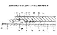
第1の実施の形態の光モジュールについて、図1〜図4に基づき説明する。図1は、本実施の形態の光モジュールの分解斜視図であり、図2は、光モジュールの要部の上面図であり、図3は、光モジュールの回路図であり、図4は、光モジュールの要部の断面図である。[First Embodiment]
(Optical module)
The optical module of 1st Embodiment is demonstrated based on FIGS. 1-4. FIG. 1 is an exploded perspective view of the optical module of the present embodiment, FIG. 2 is a top view of the main part of the optical module, FIG. 3 is a circuit diagram of the optical module, and FIG. It is sectional drawing of the principal part of a module.
本実施の形態の光モジュールは、図1に示すように、接続基板10、光導波路20、光コネクタ30、クリップ40が下部筐体51と上部筐体52とにより形成される筐体内に入れられており、光ケーブル60が接続されている。光ケーブル60の一部は筐体に覆われている。 In the optical module of the present embodiment, as shown in FIG. 1, the
接続基板10には、FPC(Flexible Printed Circuits:フレキシブルプリント回路基板)12が接続されるFPCコネクタ11及び外部との接続のための端子17が設けられている。 The
また、図2に示すように、FPC12には、電気信号を光信号に変換し出射するVCSEL等の発光素子13、及び光信号を電気信号に変換するPD等の受光素子14が搭載されている。また、FPC12には発光素子13を駆動する駆動IC15、受光素子14から出力される電流を電圧に変換するTIA16等が設けられている。発光素子13及び受光素子14は、いわゆるフェイスダウン、即ち、発光素子13の発光面及び受光素子14の受光面が下向きとなり、FPC12と対向するように実装されている。具体的には、FPC12の一方の面に、発光素子13及び受光素子14が実装されており、FPC12の他方の面には、光導波路20が取り付けられている。尚、これらの発光素子13、受光素子14、駆動IC15、TIA16は、FPC12にフリップチップボンディングにより実装されている。 As shown in FIG. 2, the FPC 12 includes a
また、受光素子14の近傍にはコンデンサ18が設けられている。コンデンサ18は、受光素子14であるPDの検出信号を安定化させるために設けられており、PDのカソードにはコンデンサ18の一方の端子が接続されており、他方の端子はFPC12におけるシグナルグランドに接続され接地されている。図2に示す場合では、4chに対応しており、4つのコンデンサ18が設けられている。 A
具体的には、図3に示すように、受光素子14には4つのフォトダイオード14aが設けられており、各々のフォトダイオード14aのカソードが対応するコンデンサ18の一方の端子に接続されており、コンデンサ18の他方の端子はシグナルグランドに接続され接地されている。受光素子14の4つのフォトダイオード14aは、TIA16における対応するTIA回路16aに各々接続されている。受光素子14に接続されたコンデンサ18は、受光素子14の直近に設置した方が検出信号を安定化させる効果が高い。具体的には、コンデンサ18と受光素子14との接続距離が短い方が、信号の伝達特性を広帯域化させることができる。このため、FPC12の受光素子14が設けられている面の、受光素子14の近傍にコンデンサ18が設置されている。 Specifically, as shown in FIG. 3, the
コンデンサ18は、容量が数十μFであり、一般的には、大きさが1mm×0.5mm×0.5mmや、0.6mm×0.3mm×0.3mmのものが多く用いられている。本実施の形態では、一例として、大きさが、0.6mm×0.3mm×0.3mmのコンデンサ18について説明する。 The
光導波路20はフレキシブルなシート状の光導波路であり、複数のコアの周囲にクラッドが形成されており、光導波路に入射した光はコア内を伝播する。 The
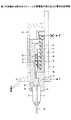
光コネクタ30は、レンズ付きフェルール31とMTフェルール32とが接続されたものである。レンズ付きフェルール31には光導波路20が接続され、光導波路20との接続部分はフェルールブーツ33により保護されている。クリップ40にはねじ穴が設けられており、クリップ40に設けられたねじ穴と下部筐体51のねじ穴51aとが、ねじ53によりねじどめされて、下部筐体51に固定されている。 The
光ケーブル60には、スリーブ61a、61bがカシメリング62により固定されている。スリーブ61a、61bが固定されている光ケーブル60の上下より、ケーブルブーツ71、72が被せられ、プルタブ/ラッチ部73が取り付けられる。 Sleeves 61 a and 61 b are fixed to the optical cable 60 by caulking rings 62.
光コネクタ30がクリップ40により固定され、FPC12を接続した接続基板10が載置された下部筐体51に上部筐体52を被せ、上部筐体52のねじ穴52aと下部筐体51のねじ穴51bとをねじ54でねじどめすることで、下部筐体51と上部筐体52が固定される。尚、下部筐体51、上部筐体52はAl等の熱伝導性の高い金属材料により形成されている。 The
本実施の形態の光モジュールは、図4に示すように、上部筐体52の内側のコンデンサ18に対向する領域に凹部55を設けた構造のものである。このように上部筐体52の内側のコンデンサ18に対向する領域に凹部55を設けて上部筐体52とコンデンサ18との間隔を静電気が放電しないように大きくすることにより、上部筐体52からコンデンサ18に静電気が流れることを防ぐことができる。 As shown in FIG. 4, the optical module of the present embodiment has a structure in which a
このことについて、図5の比較例を含めより詳細に説明する。図5は、上部筐体952の内側に凹部が設けられていない光モジュールの断面図である。上部筐体952は、内側に凹部が設けられていないことを除き上部筐体52と同じである。受光素子14やTIA16の高さは150μm〜250μmである。受光素子14及びTIA16と上部筐体952との間には、放熱シート81及び82が設置されている。放熱シート81及び82は、熱伝導性が高く、受光素子14及びTIA16において発生した熱を放熱シート81及び82を介し上部筐体952に伝え放熱する機能を有している。また、放熱シート81及び82は、弾性を有しており、何もしない状態では、厚さが、約500μmであるが、受光素子14及びTIA16と上部筐体952との間で挟まれて、放熱シート81及び82に力が加えられている状態で変形し、厚さが100μm〜200μm程度になる。 This will be described in more detail including the comparative example of FIG. FIG. 5 is a cross-sectional view of an optical module in which a recess is not provided inside the
ここで、受光素子14の高さを200μm、変形した放熱シート81の厚さを200μmとすると、FPC12と上部筐体952との間隔taは400μmとなる。受光素子14に接続されているコンデンサ18の高さが0.3mm(300μm)であるとすると、コンデンサ18と上部筐体952との間隔tbは100μmとなり、FPC12と上部筐体952との間隔taと比べて極めて狭い。このため、静電気が上部筐体952に流れ込むと、流れ込んだ静電気は、放電により上部筐体952からコンデンサ18の電極に伝わりやすく、シグナルグランドに流れ込んでしまい、光モジュールの故障の原因となりやすい。 Here, if the height of the
本実施の形態においては、図4に示すように、上部筐体52の内側において、コンデンサ18に対向する領域に凹部55が設けられている。本実施の形態の光モジュールにおいても、FPC12の一方の面12aに、受光素子14及びTIA16が取り付けられており、受光素子14及びTIA16と上部筐体52との間には、放熱シート81及び82が設置されている。尚、FPC12の他方の面12bには、光導波路20が取り付けられている。 In the present embodiment, as shown in FIG. 4, a
放熱シート81及び82は放熱部材であり、絶縁性を有し、熱伝導率が比較的高い材料により形成されている。具体的には、放熱シート81及び82は、シリコンゴム、シリコングリス、アルミナフィラを有するエポキシ樹脂等により形成されている。放熱シート81及び82は熱伝導性が高いため、受光素子14及びTIA16において発生した熱を放熱シート81及び82を介し上部筐体52に円滑に伝えることができる。これにより、上部筐体52より放熱することができる。また、放熱シート81及び82は弾性を有しており、通常の厚さは約500μmであるが、受光素子14及びTIA16と上部筐体52との間で挟まれて、力が加えられていると変形し、厚さが100μm〜200μm程度になる。 The
ここで、受光素子14の高さを200μm、変形した放熱シート81の厚さを200μmとすると、FPC12と上部筐体52との間隔tcは400μmとなる。受光素子14に接続されているコンデンサ18の高さが0.3mm(300μm)であるとすると、凹部55の深さdsは、底面55aとコンデンサ18との間隔tsが、凹部55を除く上部筐体52の内側とFPC12との間隔tcよりも大きくなるように形成されている。従って、凹部55は間隔tsが400μmよりも大きくなるように形成されており、凹部55の深さdsは300μmよりも深くなっている。このような深さdsの凹部55を上部筐体52の内側に形成することにより、静電気が上部筐体52に流れ込んでも、上部筐体52からコンデンサ18の電極への放電を防ぐことができる。 Here, if the height of the
即ち、FPC12と上部筐体52との間隔tcは、上部筐体52に静電気が流れ込んでも、上部筐体52からFPC12に形成された電極に放電しないような間隔で形成されているため、凹部55の底面55aとコンデンサ18との間隔tsが、FPC12と上部筐体52との間隔tcよりも広くなるような深さdsの凹部55を上部筐体52の内側に設けることにより、上部筐体52に静電気が流れ込んでも、上部筐体52からコンデンサ18に放電することを防ぐことができる。 That is, the interval tc between the
従って、本実施の形態においては、図6に模式的に示すように、フレーム91に流れ込んだ静電気は、ケース92、本実施の形態における光モジュールの上部筐体52及び下部筐体51を介し、再びフレーム91に流れてフレームグランド(FG)に流れる。従って、静電気が上部筐体52からコンデンサ18の電極等に放電することはないため、FPC12のシグナルグランド(SG)に静電気が流れ込むことはない。これにより、本実施の形態においては、光モジュールの信頼性を高めることができる。 Therefore, in the present embodiment, as schematically shown in FIG. 6, static electricity flowing into the
尚、図5に示される構造の光モジュールにおいて、コンデンサ18と上部筐体952との距離を離すことにより、上部筐体952に静電気が流れ込んでも、放電によりコンデンサ18に静電気が流れ込むことを抑制することが可能であるが、この場合には、光モジュール全体の大きさが大きくなるため、光モジュールの小型化の要求を満足させることができない可能性もある。 In the optical module having the structure shown in FIG. 5, it is possible to prevent static electricity from flowing into the
尚、本実施の形態においては、図4におけるコンデンサ18の一方の端子から他方の端子まで(図4における)左右方向の長さLを0.6mm(600μm)とした場合には、凹部55の左右方向の幅Wは、コンデンサ18の一方の端子側および他方の端子側に、各々FPC12と上部筐体52との間隔tcよりも大きな間隔を設け、L+2tc以上、即ち、600μm+2×400μm=1400μm(1.4mm)以上とすることで、コンデンサ18の長さ方向においても上部筐体52からコンデンサ18への静電気の放電を防ぐことができるため好ましい。 In the present embodiment, when the length L in the left-right direction (in FIG. 4) from one terminal to the other terminal of the
〔第2の実施の形態〕
次に、第2の実施の形態の光モジュールについて説明する。本実施の形態の光モジュールは、図7に示されるように、上部筐体52の内側に形成された凹部55に絶縁体155を埋め込んだ構造の光モジュールである。このように凹部55に絶縁体155を埋め込むことにより、上部筐体52とコンデンサ18の電極との間における空気中の放電を防ぐことができ、より信頼性を向上させることができる。[Second Embodiment]
Next, an optical module according to a second embodiment will be described. As shown in FIG. 7, the optical module of the present embodiment is an optical module having a structure in which an
絶縁体155を形成する材料としては、酸化シリコンや酸化アルミニウム等の絶縁性を有する酸化物、ポリイミド等の絶縁性を有する樹脂材料等が挙げられる。また、上部筐体52とコンデンサ18との間に大きな静電容量が形成されることを防ぐため、絶縁体155は、比誘電率が低い材料により形成されていることが好ましい。また、絶縁体155に樹脂材料を用いた場合には、樹脂材料は凹部55を容易に埋め込むことができ、低コストで本実施の形態の光モジュールを製造することができるため好ましい。 As a material for forming the
尚、上記以外の内容については、第1の実施の形態と同様である。 The contents other than the above are the same as in the first embodiment.
以上、本発明の実施に係る形態について説明したが、上記内容は、発明の内容を限定するものではない。 As mentioned above, although the form which concerns on implementation of this invention was demonstrated, the said content does not limit the content of invention.
10 接続基板
11 FPCコネクタ
12 FPC(基板)
13 発光素子
14 受光素子
15 駆動IC
16 TIA
18 コンデンサ
20 光導波路
51 下部筐体
52 上部筐体
55 凹部
81 放熱シート
82 放熱シート10
13 Light-Emitting
16 TIA
18
Claims (5)
Translated fromJapanese前記受光素子に接続されており、前記基板の一方の面に設置されているコンデンサと、
前記基板の他方の面に取り付けられ光を伝播する光導波路と、
前記基板を覆う筐体と、
を有し、
前記筐体の内側の前記コンデンサと対向する面には凹部が形成されていることを特徴とする光モジュール。A light receiving element provided on one surface of the substrate;
A capacitor connected to the light receiving element and installed on one surface of the substrate;
An optical waveguide attached to the other surface of the substrate for propagating light;
A housing covering the substrate;
Have
An optical module, wherein a concave portion is formed on a surface of the housing facing the capacitor.
前記フォトダイオードのカソードには、前記コンデンサの一方の端子が接続されており、
前記コンデンサの他方の端子は接地されていることを特徴とする請求項1または2に記載の光モジュール。The light receiving element is a photodiode,
One terminal of the capacitor is connected to the cathode of the photodiode,
The optical module according to claim 1, wherein the other terminal of the capacitor is grounded.
Priority Applications (2)
| Application Number | Priority Date | Filing Date | Title |
|---|---|---|---|
| JP2016218968AJP2018077344A (en) | 2016-11-09 | 2016-11-09 | Optical module |
| US15/722,297US10382142B2 (en) | 2016-11-09 | 2017-10-02 | Optical module |
Applications Claiming Priority (1)
| Application Number | Priority Date | Filing Date | Title |
|---|---|---|---|
| JP2016218968AJP2018077344A (en) | 2016-11-09 | 2016-11-09 | Optical module |
Publications (1)
| Publication Number | Publication Date |
|---|---|
| JP2018077344Atrue JP2018077344A (en) | 2018-05-17 |
Family
ID=62064881
Family Applications (1)
| Application Number | Title | Priority Date | Filing Date |
|---|---|---|---|
| JP2016218968APendingJP2018077344A (en) | 2016-11-09 | 2016-11-09 | Optical module |
Country Status (2)
| Country | Link |
|---|---|
| US (1) | US10382142B2 (en) |
| JP (1) | JP2018077344A (en) |
Cited By (1)
| Publication number | Priority date | Publication date | Assignee | Title |
|---|---|---|---|---|
| CN114895410A (en)* | 2022-05-27 | 2022-08-12 | 武汉光迅科技股份有限公司 | High-speed light emitting assembly based on inverted PLC chip and manufacturing method thereof |
Families Citing this family (5)
| Publication number | Priority date | Publication date | Assignee | Title |
|---|---|---|---|---|
| CN108873188A (en)* | 2018-06-14 | 2018-11-23 | 宁波环球广电科技有限公司 | The ejection structure of optical module |
| JP7243449B2 (en)* | 2019-05-24 | 2023-03-22 | 富士通オプティカルコンポーネンツ株式会社 | optical module |
| USD948456S1 (en)* | 2019-08-08 | 2022-04-12 | Optoway Technology Inc. | Small form-factor pluggable module |
| US11275223B1 (en)* | 2020-09-04 | 2022-03-15 | Prime World International Holdings Ltd. | Optical transceiver |
| US12360323B2 (en)* | 2022-10-18 | 2025-07-15 | Mellanox Technologies, Ltd | Mechanical thermal interface for improved heat dissipation in network transceivers |
Family Cites Families (13)
| Publication number | Priority date | Publication date | Assignee | Title |
|---|---|---|---|---|
| JP3740748B2 (en)* | 1996-06-18 | 2006-02-01 | 松下電器産業株式会社 | Optical fiber module |
| JPH11119064A (en)* | 1997-10-17 | 1999-04-30 | Fujitsu Ltd | Optical transmission terminal |
| US6869230B2 (en)* | 2002-07-02 | 2005-03-22 | Sae Magnetics (Hong Kong) | Assembly for high-speed optical transmitter or receiver |
| US6894266B2 (en)* | 2003-02-14 | 2005-05-17 | Oplink Communications, Inc. | Single chip ASIC and compact packaging solution for an avalanche photodiode (APD) and bias circuit |
| JP2009232380A (en) | 2008-03-25 | 2009-10-08 | Nec Corp | Photo-detection power monitor circuit, optical transceiver, optical module, optical receiver, amplifier circuit, and integrated circuit |
| JP5548270B2 (en)* | 2009-08-21 | 2014-07-16 | アップル インコーポレイテッド | Capacitive sensing method and apparatus |
| JP5707795B2 (en)* | 2010-09-09 | 2015-04-30 | 富士通株式会社 | Connector, optical transmission device and connector connection method |
| KR101430634B1 (en)* | 2010-11-19 | 2014-08-18 | 한국전자통신연구원 | Optical Modules |
| JP5625918B2 (en)* | 2011-01-04 | 2014-11-19 | 富士通株式会社 | Optical receiver and optical transmitter |
| JP2013098292A (en)* | 2011-10-31 | 2013-05-20 | Yamaichi Electronics Co Ltd | Optical module |
| US9780882B2 (en)* | 2014-05-13 | 2017-10-03 | Sumitomo Electric Industries, Ltd. | Optical transmitter module having multiple signal lanes |
| US9768872B2 (en)* | 2014-11-20 | 2017-09-19 | Sumitomo Electric Industries, Ltd. | Optical transceiver outputting wavelength multiplexed signal and receiving another wavelength multiplexed signal |
| US9794017B2 (en)* | 2015-08-12 | 2017-10-17 | Finisar Corporation | SWDM OSAs |
- 2016
- 2016-11-09JPJP2016218968Apatent/JP2018077344A/enactivePending
- 2017
- 2017-10-02USUS15/722,297patent/US10382142B2/ennot_activeExpired - Fee Related
Cited By (2)
| Publication number | Priority date | Publication date | Assignee | Title |
|---|---|---|---|---|
| CN114895410A (en)* | 2022-05-27 | 2022-08-12 | 武汉光迅科技股份有限公司 | High-speed light emitting assembly based on inverted PLC chip and manufacturing method thereof |
| CN114895410B (en)* | 2022-05-27 | 2023-08-29 | 武汉光迅科技股份有限公司 | High-speed light emitting assembly based on inverted PLC chip and manufacturing method thereof |
Also Published As
| Publication number | Publication date |
|---|---|
| US20180131448A1 (en) | 2018-05-10 |
| US10382142B2 (en) | 2019-08-13 |
Similar Documents
| Publication | Publication Date | Title |
|---|---|---|
| JP2018077344A (en) | Optical module | |
| US9791647B2 (en) | Optoelectronic module with improved heat management | |
| EP2428828B1 (en) | Miniaturized high speed optical module | |
| US11415764B2 (en) | Optical module | |
| JP4743107B2 (en) | Photoelectric wiring member | |
| US20230046449A1 (en) | Photoelectric conversion module | |
| KR20150032623A (en) | Optical transmission module | |
| JP6234036B2 (en) | Optical communication device | |
| JP2010176010A (en) | Optical communication device | |
| JP2018097263A (en) | Optical module | |
| US20180011264A1 (en) | Optical module | |
| JP2007019411A (en) | Optical-to-electrical transducer | |
| JP2011029504A (en) | Mounting structure | |
| US20170219787A1 (en) | Communication Module | |
| TW202109107A (en) | Opto-electro transmission module | |
| US10386592B2 (en) | Optical engine and optical module | |
| JP4882481B2 (en) | Optical module having connection structure with flexible circuit board | |
| JP2012069882A (en) | Optical module | |
| JP4856028B2 (en) | Optical module | |
| TWI896588B (en) | Photoelectric conversion module | |
| JP4935936B2 (en) | Photoelectric wiring member | |
| US20150177468A1 (en) | Optical connector | |
| JP5047388B2 (en) | Optical module | |
| KR20240146554A (en) | Photoelectric composite transmission module and optical communication cable using photoelectric composite transmission module | |
| TW202146954A (en) | Optical-electric mixed board and optical-electric composite transmission module |