JP2018060319A - Display device with touch detection function and touch detection method - Google Patents
Display device with touch detection function and touch detection methodDownload PDFInfo
- Publication number
- JP2018060319A JP2018060319AJP2016196510AJP2016196510AJP2018060319AJP 2018060319 AJP2018060319 AJP 2018060319AJP 2016196510 AJP2016196510 AJP 2016196510AJP 2016196510 AJP2016196510 AJP 2016196510AJP 2018060319 AJP2018060319 AJP 2018060319A
- Authority
- JP
- Japan
- Prior art keywords
- period
- display
- touch detection
- touch
- frame
- Prior art date
- Legal status (The legal status is an assumption and is not a legal conclusion. Google has not performed a legal analysis and makes no representation as to the accuracy of the status listed.)
- Pending
Links
Images


Classifications
- G—PHYSICS
- G06—COMPUTING OR CALCULATING; COUNTING
- G06F—ELECTRIC DIGITAL DATA PROCESSING
- G06F3/00—Input arrangements for transferring data to be processed into a form capable of being handled by the computer; Output arrangements for transferring data from processing unit to output unit, e.g. interface arrangements
- G06F3/01—Input arrangements or combined input and output arrangements for interaction between user and computer
- G06F3/03—Arrangements for converting the position or the displacement of a member into a coded form
- G06F3/041—Digitisers, e.g. for touch screens or touch pads, characterised by the transducing means
- G06F3/0412—Digitisers structurally integrated in a display
- G—PHYSICS
- G06—COMPUTING OR CALCULATING; COUNTING
- G06F—ELECTRIC DIGITAL DATA PROCESSING
- G06F3/00—Input arrangements for transferring data to be processed into a form capable of being handled by the computer; Output arrangements for transferring data from processing unit to output unit, e.g. interface arrangements
- G06F3/01—Input arrangements or combined input and output arrangements for interaction between user and computer
- G06F3/03—Arrangements for converting the position or the displacement of a member into a coded form
- G06F3/041—Digitisers, e.g. for touch screens or touch pads, characterised by the transducing means
- G06F3/0416—Control or interface arrangements specially adapted for digitisers
- G06F3/04166—Details of scanning methods, e.g. sampling time, grouping of sub areas or time sharing with display driving
- G—PHYSICS
- G06—COMPUTING OR CALCULATING; COUNTING
- G06F—ELECTRIC DIGITAL DATA PROCESSING
- G06F3/00—Input arrangements for transferring data to be processed into a form capable of being handled by the computer; Output arrangements for transferring data from processing unit to output unit, e.g. interface arrangements
- G06F3/01—Input arrangements or combined input and output arrangements for interaction between user and computer
- G06F3/03—Arrangements for converting the position or the displacement of a member into a coded form
- G06F3/041—Digitisers, e.g. for touch screens or touch pads, characterised by the transducing means
- G06F3/0416—Control or interface arrangements specially adapted for digitisers
- G06F3/0418—Control or interface arrangements specially adapted for digitisers for error correction or compensation, e.g. based on parallax, calibration or alignment
- G06F3/04184—Synchronisation with the driving of the display or the backlighting unit to avoid interferences generated internally
- G—PHYSICS
- G06—COMPUTING OR CALCULATING; COUNTING
- G06F—ELECTRIC DIGITAL DATA PROCESSING
- G06F3/00—Input arrangements for transferring data to be processed into a form capable of being handled by the computer; Output arrangements for transferring data from processing unit to output unit, e.g. interface arrangements
- G06F3/01—Input arrangements or combined input and output arrangements for interaction between user and computer
- G06F3/03—Arrangements for converting the position or the displacement of a member into a coded form
- G06F3/041—Digitisers, e.g. for touch screens or touch pads, characterised by the transducing means
- G06F3/044—Digitisers, e.g. for touch screens or touch pads, characterised by the transducing means by capacitive means
- G06F3/0443—Digitisers, e.g. for touch screens or touch pads, characterised by the transducing means by capacitive means using a single layer of sensing electrodes
- G—PHYSICS
- G06—COMPUTING OR CALCULATING; COUNTING
- G06F—ELECTRIC DIGITAL DATA PROCESSING
- G06F3/00—Input arrangements for transferring data to be processed into a form capable of being handled by the computer; Output arrangements for transferring data from processing unit to output unit, e.g. interface arrangements
- G06F3/01—Input arrangements or combined input and output arrangements for interaction between user and computer
- G06F3/03—Arrangements for converting the position or the displacement of a member into a coded form
- G06F3/041—Digitisers, e.g. for touch screens or touch pads, characterised by the transducing means
- G06F3/044—Digitisers, e.g. for touch screens or touch pads, characterised by the transducing means by capacitive means
- G06F3/0445—Digitisers, e.g. for touch screens or touch pads, characterised by the transducing means by capacitive means using two or more layers of sensing electrodes, e.g. using two layers of electrodes separated by a dielectric layer
- G—PHYSICS
- G06—COMPUTING OR CALCULATING; COUNTING
- G06F—ELECTRIC DIGITAL DATA PROCESSING
- G06F3/00—Input arrangements for transferring data to be processed into a form capable of being handled by the computer; Output arrangements for transferring data from processing unit to output unit, e.g. interface arrangements
- G06F3/01—Input arrangements or combined input and output arrangements for interaction between user and computer
- G06F3/03—Arrangements for converting the position or the displacement of a member into a coded form
- G06F3/041—Digitisers, e.g. for touch screens or touch pads, characterised by the transducing means
- G06F3/044—Digitisers, e.g. for touch screens or touch pads, characterised by the transducing means by capacitive means
- G06F3/0446—Digitisers, e.g. for touch screens or touch pads, characterised by the transducing means by capacitive means using a grid-like structure of electrodes in at least two directions, e.g. using row and column electrodes
- G—PHYSICS
- G09—EDUCATION; CRYPTOGRAPHY; DISPLAY; ADVERTISING; SEALS
- G09G—ARRANGEMENTS OR CIRCUITS FOR CONTROL OF INDICATING DEVICES USING STATIC MEANS TO PRESENT VARIABLE INFORMATION
- G09G3/00—Control arrangements or circuits, of interest only in connection with visual indicators other than cathode-ray tubes
- G09G3/20—Control arrangements or circuits, of interest only in connection with visual indicators other than cathode-ray tubes for presentation of an assembly of a number of characters, e.g. a page, by composing the assembly by combination of individual elements arranged in a matrix no fixed position being assigned to or needed to be assigned to the individual characters or partial characters
- G09G3/34—Control arrangements or circuits, of interest only in connection with visual indicators other than cathode-ray tubes for presentation of an assembly of a number of characters, e.g. a page, by composing the assembly by combination of individual elements arranged in a matrix no fixed position being assigned to or needed to be assigned to the individual characters or partial characters by control of light from an independent source
- G09G3/36—Control arrangements or circuits, of interest only in connection with visual indicators other than cathode-ray tubes for presentation of an assembly of a number of characters, e.g. a page, by composing the assembly by combination of individual elements arranged in a matrix no fixed position being assigned to or needed to be assigned to the individual characters or partial characters by control of light from an independent source using liquid crystals
- G09G3/3611—Control of matrices with row and column drivers
- G09G3/3614—Control of polarity reversal in general
- G—PHYSICS
- G09—EDUCATION; CRYPTOGRAPHY; DISPLAY; ADVERTISING; SEALS
- G09G—ARRANGEMENTS OR CIRCUITS FOR CONTROL OF INDICATING DEVICES USING STATIC MEANS TO PRESENT VARIABLE INFORMATION
- G09G3/00—Control arrangements or circuits, of interest only in connection with visual indicators other than cathode-ray tubes
- G09G3/20—Control arrangements or circuits, of interest only in connection with visual indicators other than cathode-ray tubes for presentation of an assembly of a number of characters, e.g. a page, by composing the assembly by combination of individual elements arranged in a matrix no fixed position being assigned to or needed to be assigned to the individual characters or partial characters
- G09G3/34—Control arrangements or circuits, of interest only in connection with visual indicators other than cathode-ray tubes for presentation of an assembly of a number of characters, e.g. a page, by composing the assembly by combination of individual elements arranged in a matrix no fixed position being assigned to or needed to be assigned to the individual characters or partial characters by control of light from an independent source
- G09G3/36—Control arrangements or circuits, of interest only in connection with visual indicators other than cathode-ray tubes for presentation of an assembly of a number of characters, e.g. a page, by composing the assembly by combination of individual elements arranged in a matrix no fixed position being assigned to or needed to be assigned to the individual characters or partial characters by control of light from an independent source using liquid crystals
- G09G3/3611—Control of matrices with row and column drivers
- G09G3/3648—Control of matrices with row and column drivers using an active matrix
- G—PHYSICS
- G06—COMPUTING OR CALCULATING; COUNTING
- G06F—ELECTRIC DIGITAL DATA PROCESSING
- G06F2203/00—Indexing scheme relating to G06F3/00 - G06F3/048
- G06F2203/041—Indexing scheme relating to G06F3/041 - G06F3/045
- G06F2203/04112—Electrode mesh in capacitive digitiser: electrode for touch sensing is formed of a mesh of very fine, normally metallic, interconnected lines that are almost invisible to see. This provides a quite large but transparent electrode surface, without need for ITO or similar transparent conductive material
- G—PHYSICS
- G09—EDUCATION; CRYPTOGRAPHY; DISPLAY; ADVERTISING; SEALS
- G09G—ARRANGEMENTS OR CIRCUITS FOR CONTROL OF INDICATING DEVICES USING STATIC MEANS TO PRESENT VARIABLE INFORMATION
- G09G2310/00—Command of the display device
- G09G2310/08—Details of timing specific for flat panels, other than clock recovery
- G—PHYSICS
- G09—EDUCATION; CRYPTOGRAPHY; DISPLAY; ADVERTISING; SEALS
- G09G—ARRANGEMENTS OR CIRCUITS FOR CONTROL OF INDICATING DEVICES USING STATIC MEANS TO PRESENT VARIABLE INFORMATION
- G09G2354/00—Aspects of interface with display user
Landscapes
- Engineering & Computer Science (AREA)
- Theoretical Computer Science (AREA)
- General Engineering & Computer Science (AREA)
- Physics & Mathematics (AREA)
- General Physics & Mathematics (AREA)
- Human Computer Interaction (AREA)
- Chemical & Material Sciences (AREA)
- Crystallography & Structural Chemistry (AREA)
- Computer Hardware Design (AREA)
- Control Of Indicators Other Than Cathode Ray Tubes (AREA)
- Liquid Crystal Display Device Control (AREA)
- Liquid Crystal (AREA)
Abstract
Translated fromJapaneseDescription
Translated fromJapanese本発明は、タッチ検出機能付き表示装置及びタッチ検出方法に関する。 The present invention relates to a display device with a touch detection function and a touch detection method.
近年では、例えばスマートフォン及びタブレットコンピュータのような電子機器が広く普及している。このような電子機器においては、タッチ検出機能を有する表示装置(以下、タッチ検出機能付き表示装置と表記)が採用されている。
静電容量方式を採用したタッチ検出機能付き表示装置においては、例えば、ストライプ状に形成される駆動電極と検出電極が互いに交差するように配置されている。このタッチ検出機能付き表示装置の画面に指先が接触された場合には、駆動電極と検出電極とが交差する部分における静電容量(値)が変化する。静電容量方式においては、このような静電容量の変化を利用して画面に対する指先の接触を検出することができる。In recent years, electronic devices such as smartphones and tablet computers have become widespread. In such an electronic device, a display device having a touch detection function (hereinafter referred to as a display device with a touch detection function) is employed.
In a display device with a touch detection function that employs an electrostatic capacitance method, for example, drive electrodes and detection electrodes formed in a stripe shape are arranged so as to cross each other. When the fingertip is brought into contact with the screen of the display device with a touch detection function, the capacitance (value) at the portion where the drive electrode and the detection electrode intersect changes. In the capacitance method, it is possible to detect the contact of the fingertip with the screen using such a change in capacitance.
また、静電容量方式を採用したタッチ検出機能付き表示装置に関して、2次元配列された画素が有する画像表示用の電極(共通電極)を上記した駆動電極として兼用することによって、当該装置の薄型化及び画質の向上を実現する技術が提案されている。
このような技術において、1フレームの画像が表示される期間(1フレーム期間)には、画像表示のための表示動作が行われる表示期間及びタッチ検出のためのタッチ検出動作が行われるタッチ検出期間が交互に配置される。なお、1フレーム期間の前後には、垂直バックポーチ期間及び垂直フロントポーチ期間と称される表示調整期間が設けられている。In addition, regarding a display device with a touch detection function that employs a capacitance method, the image display electrode (common electrode) included in the two-dimensionally arranged pixels is also used as the drive electrode described above, thereby reducing the thickness of the device. In addition, techniques for improving image quality have been proposed.
In such a technique, in a period in which an image of one frame is displayed (one frame period), a display period in which a display operation for image display is performed and a touch detection period in which a touch detection operation for touch detection is performed. Are alternately arranged. Note that a display adjustment period called a vertical back porch period and a vertical front porch period is provided before and after one frame period.
ここで、タッチ検出機能付き表示装置の通常駆動時における画像(映像)のリフレッシュレート(フレームレート)が例えば60Hzであるものとすると、消費電力を低減させるために例えばリフレッシュレートを30Hzとしてタッチ検出機能付き表示装置を低速駆動させる場合がある。 Here, assuming that the refresh rate (frame rate) of the image (video) during normal driving of the display device with a touch detection function is, for example, 60 Hz, the touch detection function has a refresh rate of, for example, 30 Hz in order to reduce power consumption. The attached display device may be driven at a low speed.
この場合には通常駆動時と比較して1フレーム期間が長くなるが、上記した表示期間及びタッチ検出期間は変更せず、例えば表示調整期間を延長することによって低速駆動を実現する場合がある。 In this case, one frame period is longer than that during normal driving, but the display period and the touch detection period described above are not changed, and for example, low-speed driving may be realized by extending the display adjustment period.
しかしながら、表示調整期間期間中にタッチ検出動作が行われないため、表示調整期間を延長した場合にはタッチ検出感度(レポートレート)が低下する。
そこで、本発明が解決しようとする課題は、消費電力を低減させ、かつ、タッチ検出感度の低下を抑制することが可能なタッチ検出機能付き表示装置及びタッチ検出方法を提供することにある。However, since the touch detection operation is not performed during the display adjustment period, the touch detection sensitivity (report rate) decreases when the display adjustment period is extended.
Accordingly, the problem to be solved by the present invention is to provide a display device with a touch detection function and a touch detection method capable of reducing power consumption and suppressing a decrease in touch detection sensitivity.
本実施形態に係るタッチ検出機能付き表示装置は、表示部と、検出部と、制御部とを具備する。前記表示部は、画素信号に基づいて画像を表示するための表示動作を行う。前記検出部は、前記表示動作が行われる表示期間とは異なる第1のタッチ検出期間において、外部近接物体に応じた検出信号を検出するためのタッチ検出動作を行う。前記制御部は、前記表示動作及び前記タッチ検出動作を制御する。前記表示動作によって1フレームの画像が表示される1フレーム期間は、前記表示期間、前記第1タッチ検出期間及び前記画像の表示を調整するための表示調整期間を含む。前記制御部は、通常駆動時の第1の1フレーム期間よりも長い第2のフレーム期間で低速駆動する場合に前記表示調整期間を延長し、当該延長された表示調整期間に前記タッチ検出動作が行われる第2のタッチ検出期間を割り当てる。 The display device with a touch detection function according to the present embodiment includes a display unit, a detection unit, and a control unit. The display unit performs a display operation for displaying an image based on the pixel signal. The detection unit performs a touch detection operation for detecting a detection signal corresponding to an external proximity object in a first touch detection period different from a display period in which the display operation is performed. The control unit controls the display operation and the touch detection operation. One frame period in which an image of one frame is displayed by the display operation includes the display period, the first touch detection period, and a display adjustment period for adjusting the display of the image. The control unit extends the display adjustment period when driving at low speed in a second frame period longer than the first one frame period during normal driving, and the touch detection operation is performed during the extended display adjustment period. A second touch detection period to be performed is assigned.
以下、図面を参照して、実施形態について説明する。
図1は、本実施形態に係るタッチ検出機能付き表示装置DSPの概略構成を示す斜視図である。タッチ検出機能付き表示装置としては、表示装置の表示面上にタッチパネルを形成したいわゆるオンセル型と称されるタッチ検出機構を備えるものの他に、表示装置にもともと備えられている画像表示用の共通電極を、一対のタッチ検出用の電極のうちの一方として兼用し、他方の電極(タッチ検出電極)をこの共通電極と交差するように配置した、いわゆるインセル型と称されるタッチ検出機構を備えるものがある。以下の説明において、本実施形態に係るタッチ検出機能付き表示装置(以下、単に表示装置と表記)DSPはインセル型と称されるタッチ検出機構を備えるものとして説明する。Hereinafter, embodiments will be described with reference to the drawings.
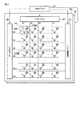
FIG. 1 is a perspective view showing a schematic configuration of a display device DSP with a touch detection function according to the present embodiment. As a display device with a touch detection function, in addition to a so-called on-cell type touch detection mechanism in which a touch panel is formed on the display surface of the display device, a common electrode for image display originally provided in the display device With a so-called in-cell type touch detection mechanism in which the other electrode (touch detection electrode) is arranged so as to intersect with the common electrode. There is. In the following description, a display device with a touch detection function (hereinafter simply referred to as a display device) DSP according to the present embodiment will be described as including a touch detection mechanism called an in-cell type.
図1に示すように、表示装置DSPは、表示パネルPNLを備える。表示パネルPNLは、タッチ検出機構一体型の表示パネルである。表示パネルPNLとしては、表示機能層として液晶層を用いた表示パネル及び有機発光層を用いた有機エレクトロルミネッセンス(EL)パネル等が用いられるが、ここでは液晶層を用いた表示パネルについて説明する。 As shown in FIG. 1, the display device DSP includes a display panel PNL. The display panel PNL is a touch detection mechanism integrated display panel. As the display panel PNL, a display panel using a liquid crystal layer as a display function layer and an organic electroluminescence (EL) panel using an organic light emitting layer are used. Here, a display panel using a liquid crystal layer will be described.
なお、本実施形態において「タッチ検出」は、指先(またはペン)等の被検出物が表示パネルPNLに接触したことを検出することのみでなく、例えば被検出物が表示パネルPNLに近接したことを検知することをも含むものとする。
表示パネルPNLは、第1基板SUB1(アレイ基板)と、第1基板SUB1に対向配置された第2基板SUB2(対向基板)と、第1基板SUB1及び第2基板SUB2の間に形成された液晶層(図示せず)とを備える。なお、例えば第1基板SUB1上には、表示パネルPNLを駆動するパネルドライバ(液晶ドライバ)IC1が搭載されている。In the present embodiment, “touch detection” not only detects that a detected object such as a fingertip (or pen) touches the display panel PNL, but also, for example, indicates that the detected object is close to the display panel PNL. It also includes detecting the above.
The display panel PNL includes a first substrate SUB1 (array substrate), a second substrate SUB2 (counter substrate) disposed opposite to the first substrate SUB1, and a liquid crystal formed between the first substrate SUB1 and the second substrate SUB2. A layer (not shown). For example, a panel driver (liquid crystal driver) IC1 for driving the display panel PNL is mounted on the first substrate SUB1.
表示パネルPNLは、例えば容量変化検出型のタッチ検出機構SEと一体化して構成されている。図1において、表示パネルPNLの表示領域DAの面上には、タッチ検出機構SEを形成するタッチ検出電極Rxが設けられている。タッチ検出電極Rxは、例えば透明電極であり、ITO(インジウム・ティン・オキサイド)等で構成される。なお、タッチ検出電極Rxは、表示パネルPNLの外部に設けられていてもよいし、内部に設けられていてもよい。タッチ検出機構SEは、タッチドライバIC2により制御される。 The display panel PNL is configured integrally with a capacitance change detection type touch detection mechanism SE, for example. In FIG. 1, a touch detection electrode Rx that forms a touch detection mechanism SE is provided on the surface of the display area DA of the display panel PNL. The touch detection electrode Rx is a transparent electrode, for example, and is made of ITO (indium tin oxide) or the like. Note that the touch detection electrode Rx may be provided outside the display panel PNL or may be provided inside. The touch detection mechanism SE is controlled by the touch driver IC2.
また、表示装置DSPの外部にはホスト装置HOSが設けられ、当該ホスト装置HOSは、フレキシブル配線基板FPC1及びパネルドライバIC1を介して、表示パネルPNLに接続されている。また、ホスト装置HOSは、フレキシブル配線基板FPC2及びタッチドライバIC2を介して、タッチ検出機構SEに接続されている。 A host device HOS is provided outside the display device DSP, and the host device HOS is connected to the display panel PNL via the flexible wiring board FPC1 and the panel driver IC1. The host device HOS is connected to the touch detection mechanism SE via the flexible wiring board FPC2 and the touch driver IC2.
なお、パネルドライバIC1及びタッチドライバIC2は、同一チップとして構成されていても構わない。タッチドライバIC2をパネルドライバIC1と同一チップとする場合には、当該チップを例えば第2基板SUB2、フレキシブル配線基板FPC1またはフレキシブル配線基板FPC2上に配置することにより、フレキシブル配線基板FPC1及びフレキシブル配線基板FPC2の一方を省略してもよい。 Note that the panel driver IC 1 and the touch driver IC 2 may be configured as the same chip. When the touch driver IC2 is the same chip as the panel driver IC1, the flexible circuit board FPC1 and the flexible wiring board FPC2 are arranged by arranging the chip on the second substrate SUB2, the flexible wiring board FPC1, or the flexible wiring board FPC2, for example. One of these may be omitted.
第1基板SUB1の下側(つまり、表示パネルPNLの背面側)には、表示パネルPNLを照明する照明具としてバックライトユニットBLが配置されている。フレキシブル配線基板FPC3は、バックライトユニットBLとホスト装置HOSとを接続する。バックライトユニットBLとしては、種々の形態のバックライトユニットが利用可能であり、光源としては、発光ダイオード(LED)を利用したもの及び冷陰極管(CCFL)を利用したもの等がある。ここでは、表示パネルPNLの背面側に配置されるバックライトユニットBLを使用する場合について説明したが、当該表示パネルPNLの表示面側に配置されるフロントライトが使用されても構わない。また、導光板とそのサイドに配置されるLEDまたは冷陰極管を用いた照明具が使用されてもよいし、発光素子を平面的に配列した点状光源を用いた照明具が使用されてもよい。なお、表示装置DSPが反射型の表示装置である場合、または表示パネルPNLが有機ELを用いている場合には、照明具を備えない構成であってもよい。
図1においては省略されているが、表示装置DSPは、2次電池及び電源回路等を備える。On the lower side of the first substrate SUB1 (that is, the back side of the display panel PNL), a backlight unit BL is disposed as a lighting tool that illuminates the display panel PNL. The flexible wiring board FPC3 connects the backlight unit BL and the host device HOS. Various types of backlight units can be used as the backlight unit BL, and examples of the light source include those using light emitting diodes (LEDs) and those using cold cathode fluorescent lamps (CCFLs). Although the case where the backlight unit BL disposed on the back side of the display panel PNL is used has been described here, a front light disposed on the display surface side of the display panel PNL may be used. Further, a lighting device using a light guide plate and an LED or a cold cathode tube disposed on the side thereof may be used, or a lighting device using a point light source in which light emitting elements are arranged in a plane is used. Good. When the display device DSP is a reflective display device, or when the display panel PNL uses an organic EL, a configuration without an illumination tool may be used.
Although omitted in FIG. 1, the display device DSP includes a secondary battery, a power supply circuit, and the like.
なお、本実施形態の表示パネルPNLは、透過型、反射型、半透過型のいずれであってもよい。透過型の表示パネルPNLが適用された表示装置DSPには、上記の通り、第1基板SUB1の背面側にバックライトユニットBLを備え、バックライトユニットBLからの光を選択的に透過させることで画像を表示する透過表示機能を有している。反射型の表示パネルPNLが適用される表示装置DSPは、液晶層より表示パネルPNLの背面側に光を反射する反射層を有し、第2基板SUB2の前面側(あるいは表示面側)からの光を選択的に反射させることで画像を表示する反射表示機能を有している。なお、反射型の表示パネルPNLの前面側には、補助光源が備えられてもよい。また、反射層は、金属等の反射機能を有する材料で液晶層より表示パネルPNLの背面側にある電極を形成するように構成されていてもよい。半透過型の表示パネルPNLが適用される表示装置DSPは、上記の透過表示機能及び反射表示機能を有している。 Note that the display panel PNL of the present embodiment may be any of a transmissive type, a reflective type, and a transflective type. As described above, the display device DSP to which the transmissive display panel PNL is applied includes the backlight unit BL on the back side of the first substrate SUB1, and selectively transmits light from the backlight unit BL. It has a transmissive display function for displaying images. The display device DSP to which the reflective display panel PNL is applied has a reflective layer that reflects light from the liquid crystal layer to the back side of the display panel PNL, and is from the front surface side (or display surface side) of the second substrate SUB2. It has a reflective display function for displaying an image by selectively reflecting light. An auxiliary light source may be provided on the front side of the reflective display panel PNL. The reflective layer may be configured to form an electrode on the back side of the display panel PNL from the liquid crystal layer with a material having a reflective function such as metal. A display device DSP to which the transflective display panel PNL is applied has the transmissive display function and the reflective display function described above.
図2は、主として表示装置DSPに備えられる表示パネルPNLの概略構成を示す。図2に示すように、表示パネルPNLには、マトリクス状に配置された複数の表示画素PX(表示素子)が設けられている。更に、表示パネルPNLには、複数の表示画素PXが配列する行に沿って延びる走査線G(G1、G2、…、Gm)と、複数の表示画素PXが配列する列に沿って延びる信号線S(S1、S2、…、Sn)と、走査線Gと信号線Sとが交差する位置近傍に配置された画素スイッチSWとが備えられている。 FIG. 2 shows a schematic configuration of a display panel PNL mainly provided in the display device DSP. As shown in FIG. 2, the display panel PNL is provided with a plurality of display pixels PX (display elements) arranged in a matrix. Further, the display panel PNL includes scanning lines G (G1, G2,..., Gm) extending along the rows where the plurality of display pixels PX are arranged, and signal lines extending along the columns where the plurality of display pixels PX are arranged. S (S1, S2,..., Sn) and a pixel switch SW disposed near the position where the scanning line G and the signal line S intersect with each other.
画素スイッチSWは、薄膜トランジスタ(TFT:Thin Film Transistor)を含む。画素スイッチSWのゲート電極は、対応する走査線Gと電気的に接続されている。画素スイッチSWのソース電極は、対応する信号線Sと電気的に接続されている。また、画素スイッチSWのドレイン電極は、対応する画素電極PEと電気的に接続されている。なお、画素スイッチSWのソース電極が対応する画素電極PEと接続され、当該画素スイッチSWのドレイン電極が対応する信号線Sと接続される構成であってもよい。 The pixel switch SW includes a thin film transistor (TFT). The gate electrode of the pixel switch SW is electrically connected to the corresponding scanning line G. The source electrode of the pixel switch SW is electrically connected to the corresponding signal line S. Further, the drain electrode of the pixel switch SW is electrically connected to the corresponding pixel electrode PE. Note that the source electrode of the pixel switch SW may be connected to the corresponding pixel electrode PE, and the drain electrode of the pixel switch SW may be connected to the corresponding signal line S.
また、表示パネルPNLには、複数の表示画素PXを駆動するためにゲートドライバGD及びソースドライバSDが設けられている。複数の走査線Gは、ゲートドライバGDの出力端子と電気的に接続されている。複数の信号線Sは、ソースドライバSDの出力端子と電気的に接続されている。 Further, the display panel PNL is provided with a gate driver GD and a source driver SD for driving the plurality of display pixels PX. The plurality of scanning lines G are electrically connected to the output terminal of the gate driver GD. The plurality of signal lines S are electrically connected to the output terminal of the source driver SD.
ゲートドライバGDは、複数の走査線Gにオン電圧を順次印加して、選択された走査線Gに電気的に接続された画素スイッチSWのゲート電極にオン電圧を供給する。ゲート電極にオン電圧が供給された画素スイッチSWの、ソース電極−ドレイン電極間が導通する。 The gate driver GD sequentially applies an ON voltage to the plurality of scanning lines G, and supplies the ON voltage to the gate electrode of the pixel switch SW electrically connected to the selected scanning line G. The source electrode and the drain electrode of the pixel switch SW in which the ON voltage is supplied to the gate electrode are conducted.
ソースドライバSDは、複数の信号線Sのそれぞれに対応する出力信号を供給する。信号線Sに供給された信号は、ソース電極−ドレイン電極間が導通した画素スイッチSWを介して、対応する画素電極PEに印加される。
更に、表示パネルPNLは、共通電極ドライバCDを備える。共通電極ドライバCDは、表示装置DSPの共通電極COMEに駆動信号を供給する(駆動電圧を印加する)回路である。共通電極COMEについては後述するが、上記した画素電極PE及び共通電極COMEは、絶縁膜を介して対向配置されている。画素電極PE、共通電極COME及び絶縁膜は、保持容量CSを形成する。The source driver SD supplies an output signal corresponding to each of the plurality of signal lines S. The signal supplied to the signal line S is applied to the corresponding pixel electrode PE through the pixel switch SW in which the source electrode and the drain electrode are electrically connected.
Further, the display panel PNL includes a common electrode driver CD. The common electrode driver CD is a circuit that supplies a drive signal (applies a drive voltage) to the common electrode COME of the display device DSP. Although the common electrode COME will be described later, the pixel electrode PE and the common electrode COME described above are disposed to face each other via an insulating film. The pixel electrode PE, the common electrode COME, and the insulating film form a storage capacitor CS.
なお、ゲートドライバGD、ソースドライバSD及び共通電極ドライバCDは、表示パネルPNLの周囲の領域(額縁)に配置され、上記したパネルドライバIC1によって制御される。更に、パネルドライバIC1は、バックライトユニットBLの動作を制御する。 Note that the gate driver GD, the source driver SD, and the common electrode driver CD are arranged in a region (frame) around the display panel PNL, and are controlled by the panel driver IC1 described above. Further, the panel driver IC1 controls the operation of the backlight unit BL.
図2においては1つのゲートドライバGDのみが示されているが、表示パネルPNLは、複数(例えば、2つ)のゲートドライバGDを備える構成であってもよい。2つのゲートドライバを備える構成の場合、例えば複数の走査線Gのうち、一方のゲートドライバが走査線G1、G3、…、Gm−1と接続され、他方のゲートドライバが走査線G2、G4、…、Gmと接続されるように構成される。なお、2つのゲートドライバは、例えば複数の表示画素PXを挟んで対向するように配置される。 Although only one gate driver GD is shown in FIG. 2, the display panel PNL may be configured to include a plurality (for example, two) of gate drivers GD. In the case of a configuration including two gate drivers, for example, one of the plurality of scanning lines G is connected to the scanning lines G1, G3, ..., Gm-1, and the other gate driver is connected to the scanning lines G2, G4, ..., configured to be connected to Gm. Note that the two gate drivers are disposed so as to face each other with the plurality of display pixels PX interposed therebetween, for example.
図3は、表示装置DSPの断面構造を模式的に示す図(断面図)である。表示装置DSPは、表示パネルPNL、バックライトユニットBL、第1光学素子OD1及び第2光学素子OD2を備える。
なお、図3において、表示パネルPNLは、表示モードとしてFFS(Fringe Field Switching)モードに対応した構成を有しているが、他の表示モードに対応した構成を有していてもよい。FIG. 3 is a diagram (cross-sectional view) schematically showing a cross-sectional structure of the display device DSP. The display device DSP includes a display panel PNL, a backlight unit BL, a first optical element OD1, and a second optical element OD2.
In FIG. 3, the display panel PNL has a configuration corresponding to an FFS (Fringe Field Switching) mode as a display mode, but may have a configuration corresponding to another display mode.
表示パネルPNLは、上述したように第1基板SUB1、第2基板SUB2及び液晶層LQを備える。第1基板SUB1と第2基板SUB2とは、所定のセルギャップを形成した状態で貼り合わされている。液晶層LQは、第1基板SUB1と第2基板SUB2との間のセルギャップに保持されている。 As described above, the display panel PNL includes the first substrate SUB1, the second substrate SUB2, and the liquid crystal layer LQ. The first substrate SUB1 and the second substrate SUB2 are bonded together in a state where a predetermined cell gap is formed. The liquid crystal layer LQ is held in the cell gap between the first substrate SUB1 and the second substrate SUB2.
第1基板SUB1は、ガラス基板や樹脂基板等の光透過性を有する第1絶縁基板10を用いて形成されている。第1基板SUB1は、第1絶縁基板10の第2基板SUB2に対向する側に、信号線S、共通電極COME、画素電極PE、第1絶縁膜11、第2絶縁膜12、第3絶縁膜13及び第1配向膜AL1等を備える。 The first substrate SUB1 is formed using a first insulating
ここで、画素電極PE及び共通電極COMEは上記した液晶層LQの画素領域とともに表示画素PXを構成し、当該表示画素PXは、図2において説明したように表示パネルPNLにマトリクス状に配置される。
第1絶縁膜11は、第1絶縁基板10の上に配置されている。また、信号線Sは、第1絶縁膜11の上に形成されている。図3に示す例では、信号線Sは、Y方向に延出している。Here, the pixel electrode PE and the common electrode COME constitute a display pixel PX together with the pixel region of the liquid crystal layer LQ, and the display pixel PX is arranged in a matrix on the display panel PNL as described in FIG. .
The first insulating
なお、図示されていないが、第1絶縁基板10と第1絶縁膜11との間には、走査線G、スイッチング素子(画素スイッチSW)のゲート電極及び半導体層等が配置されている。更に、スイッチング素子のソース電極及びドレイン電極等も第1絶縁膜11の上に形成されている。 Although not shown, between the first insulating
第2絶縁膜12は、信号線S及び第1絶縁膜11の上に配置されている。共通電極COMEは、第2絶縁膜12の上に形成されている。共通電極COMEは、複数のセグメントによって構成されている。共通電極COMEの各セグメントは、それぞれX方向に延出し、所定の間隔でY方向に配列されている。共通電極COMEは、ITO(インジウム・ティン・オキサイド)またはIZO(インジウム・ジンク・オキサイド)等の透明な導電材料によって形成されている。図3に示す例では、共通電極COMEの上に金属層MLが形成され、当該共通電極COMEが低抵抗化されている。なお、金属層MLは省略されても構わない。 The second insulating
第3絶縁膜13は、共通電極COME及び第2絶縁膜12の上に配置されている。画素電極PEは、第3絶縁膜13の上に形成されている。各画素電極PEは、隣接する信号線Sの間にそれぞれ位置し、共通電極COMEと対向している。また、各画素電極PEは、共通電極COMEと対向する位置にスリットSLを有している。このような画素電極PEは、例えばITOまたはIZO等の透明な導電材料によって形成されている。第1配向膜AL1は、画素電極PE及び第3絶縁膜13を覆っている。 The third
一方、第2基板SUB2は、ガラス基板または樹脂基板等の光透過性を有する第2絶縁基板20を用いて形成されている。第2基板SUB2は、第2絶縁基板20の第1基板SUB1に対向する側に、ブラックマトリクスBM、カラーフィルタCFR、CFG、CFB、オーバーコート層OC及び第2配向膜AL2等を備える。 On the other hand, the second substrate SUB2 is formed using a second insulating
ブラックマトリクスBMは、第2絶縁基板20の内面に形成され、各画素を区画している。カラーフィルタCFR、CFG、CFBは、それぞれ第2絶縁基板20の内面に形成され、それらの一部がブラックマトリクスBMに重なっている。カラーフィルタCFRは赤色カラーフィルタであり、カラーフィルタCFGは緑色カラーフィルタであり、カラーフィルタCFBは青色カラーフィルタである。オーバーコート層OCは、カラーフィルタCFR、CFG、CFBを覆っている。オーバーコート層OCは、透明な樹脂材料によって形成されている。第2配向膜AL2は、オーバーコート層OCを覆っている。
なお、カラーフィルタ及びブラックマトリクス等は、第1絶縁基板10上に形成されていてもよい。また、カラーフィルタは、例えば画素電極PEの上に積層されてもよい。The black matrix BM is formed on the inner surface of the second insulating
Note that the color filter, the black matrix, and the like may be formed on the first insulating
タッチ検出電極Rxは、第2絶縁基板20の外面に形成されている。このタッチ検出電極Rxは島状に形成されているが、ここでは便宜的にリード線については省略されている。タッチ検出電極Rxは、例えば、アルミニウム(Al)、チタン(Ti)、銀(Ag)、モリブデン(Mo)、タングステン(W)、銅(Cu)、クロム(Cr)などの金属材料や、これらの金属材料を組み合わせた合金や、ITOやIZO等の透明導電材料や、導電性の有機材料や、微細な導電性物質の分散体などによって形成されている。また、タッチ検出電極Rxは、上記の材料からなる単層体であってもよいし、積層体であってもよい。積層体の一例では、タッチ検出電極Rxは、上記の金属材料からなる金属細線と、透明導電材料とを備えた構成が挙げられる。タッチ検出電極Rxに金属材料を用いる場合は、メッシュ加工を施してもよいし、黒色材料でメッキ加工するなどの不可視化処理をするとよりよい。 The touch detection electrode Rx is formed on the outer surface of the second insulating
バックライトユニットBLは、上記したように表示パネルPNLの背面側に配置されている。第1光学素子OD1は、第1絶縁基板10とバックライトユニットBLとの間に配置されている。第2光学素子OD2は、タッチ検出電極Rxの上に配置されている。第1光学素子OD1及び第2光学素子OD2は、それぞれ少なくとも偏光板を含む。また、第1光学素子OD1及び第2光学素子OD2は、必要に応じて位相差板を含む構成であってもよい。 As described above, the backlight unit BL is arranged on the back side of the display panel PNL. The first optical element OD1 is disposed between the first insulating
図4は、上記したタッチ検出機構SEの基本動作を説明するための図である。図4は、ミューチュアル(相互容量)検出方式のタッチ検出機構SEを示す。なお、タッチ検出機構SEのタッチ検出の方式は、例えばセルフ検出方式等の他の検出方式であっても構わない。 FIG. 4 is a diagram for explaining the basic operation of the touch detection mechanism SE described above. FIG. 4 shows a touch detection mechanism SE of a mutual (mutual capacitance) detection method. Note that the touch detection method of the touch detection mechanism SE may be another detection method such as a self-detection method.
ミューチュアル検出方式のタッチ検出機構SEにおいては、第2基板SUB2に例えばY方向にストライプ状に形成されるタッチ検出電極(検出素子)Rxと、第1基板SUB1にX方向にストライプ状に形成される駆動電極Txとが形成されている。すなわち、タッチ検出電極Rxと駆動電極Txとは、互いに交差する関係である。この駆動電極Txとしては、上述した画像表示用の共通電極COMEが用いられる。
なお、タッチ検出電極RxがX方向にストライプ状に形成され、駆動電極TxがY方向にストライプ状に形成されてもよい。In the mutual detection type touch detection mechanism SE, touch detection electrodes (detection elements) Rx formed in a stripe shape in the Y direction, for example, on the second substrate SUB2, and formed in a stripe shape in the X direction on the first substrate SUB1. A drive electrode Tx is formed. That is, the touch detection electrode Rx and the drive electrode Tx are in a crossing relationship with each other. As the drive electrode Tx, the above-described common electrode COME for image display is used.
Note that the touch detection electrodes Rx may be formed in a stripe shape in the X direction, and the drive electrodes Tx may be formed in a stripe shape in the Y direction.
このような構成によれば、後述するタッチ検出期間においては、駆動電極Txとして用いられる共通電極COMEが順次高周波パルスの駆動信号(タッチ駆動信号)Txsにより駆動される。この場合、例えば被検出物(外部近接物体)が近接しているタッチ検出電極Rxからは、他のタッチ検出電極Rxからの出力に比べて、レベルの低いタッチ検出信号Rxsが検出される。これは、被検出物が近接しているタッチ検出電極Rxと共通電極COMEとの間に生じている第1容量に加えて、当該タッチ検出電極Rxと被検出物との間に第2容量が発生しているためである。すなわち、タッチ検出電極Rxは、外部近接物体に応じた静電容量の変化に基づくタッチ検出信号Rxsを出力することができる。
タッチ検出機構SEによれば、上記の駆動電極Txとしての共通電極COMEの駆動タイミングと、レベルの低い検出信号Rxsを出力したタッチ検出電極Rxの位置とから、被検出物の座標位置を判定することができる。According to such a configuration, in the touch detection period described later, the common electrode COME used as the drive electrode Tx is sequentially driven by the drive signal (touch drive signal) Txs of the high frequency pulse. In this case, for example, a touch detection signal Rxs having a lower level than the output from the other touch detection electrodes Rx is detected from the touch detection electrode Rx to which the detection object (external proximity object) is close. This is because, in addition to the first capacitance generated between the touch detection electrode Rx and the common electrode COME that are to be detected, the second capacitance is provided between the touch detection electrode Rx and the detection target. This is because it has occurred. That is, the touch detection electrode Rx can output a touch detection signal Rxs based on a change in capacitance according to an external proximity object.
According to the touch detection mechanism SE, the coordinate position of the object to be detected is determined from the drive timing of the common electrode COME as the drive electrode Tx and the position of the touch detection electrode Rx that has output the low-level detection signal Rxs. be able to.
図5は、上記した共通電極COME(駆動電極Tx)とタッチ検出電極Rxとの構成例を説明するための図である。 FIG. 5 is a diagram for explaining a configuration example of the common electrode COME (drive electrode Tx) and the touch detection electrode Rx.
本実施形態に係る表示装置DSPにおいては、パネルドライバIC1(DDI)とタッチドライバIC2(TPIC)とが協働することにより、共通電極COMEには駆動パルスTSVCOM(タッチ駆動信号Txs)が入力され、タッチ検出電極Rxから検出パルス(タッチ検出信号Rxs)が得られる。また、タッチドライバIC2は、駆動パルスTSVCOMを入力した共通電極COMEの位置と、検出パルスの波形とから被検出物の接触位置を把握する。なお、接触位置(タッチ位置)の算出は、図示しない外部装置(例えば、ホスト装置HOS)によって行われても構わない。パネルドライバIC1とタッチドライバIC2との授受信号の詳細については後述する。 In the display device DSP according to the present embodiment, the panel driver IC1 (DDI) and the touch driver IC2 (TPIC) cooperate to input the driving pulse TSVCOM (touch driving signal Txs) to the common electrode COME. A detection pulse (touch detection signal Rxs) is obtained from the touch detection electrode Rx. Further, the
次に、図6を参照して、表示期間とタッチ検出期間との関係について説明する。
本実施形態において、表示期間は、表示パネルPNLにおける画像の表示動作(ゲートドライバGD及びソースドライバSDによる表示画素PXに対する駆動動作)が実行される期間を含む。一方、タッチ検出期間は、上記した共通電極COME(駆動電極Tx)にタッチ駆動信号Txsを供給してタッチ検出信号Rxsを検出するタッチ検出動作が実行される期間を含む。Next, the relationship between the display period and the touch detection period will be described with reference to FIG.
In the present embodiment, the display period includes a period during which an image display operation on the display panel PNL (a driving operation for the display pixel PX by the gate driver GD and the source driver SD) is executed. On the other hand, the touch detection period includes a period in which a touch detection operation for detecting the touch detection signal Rxs by supplying the touch drive signal Txs to the common electrode COME (drive electrode Tx) is performed.
ここで、上記したようにタッチ検出期間においてタッチ駆動信号Txsが供給される駆動電極Txとしては、複数のストライプ状の共通電極COMEが用いられる。すなわち、画像表示に使用される共通電極COMEがタッチ検出用の駆動電極Txとしても利用されるため、本実施形態においては、表示動作とタッチ検出動作とがタイムシェアリングにより行われる。 Here, as described above, a plurality of stripe-shaped common electrodes COME are used as the drive electrodes Tx to which the touch drive signal Txs is supplied in the touch detection period. That is, since the common electrode COME used for image display is also used as the drive electrode Tx for touch detection, in this embodiment, the display operation and the touch detection operation are performed by time sharing.
具体的には、図6に示すように、上記した表示動作によって1フレームの画像が表示される期間(以下、1フレーム期間と表記)は、複数のユニットで構成される。1ユニット内は、上記した表示期間及びタッチ検出期間に分割される。すなわち、1ユニット内の期間においては、RGBの3色のうちの1つを選択する信号(SELR/G/B)に対応して色毎の画素信号(SIGn)を出力する動作(表示動作)が表示期間において複数の表示行(ライン)について実行された後、駆動電極Txとしての共通電極COMEにタッチ駆動信号Txを供給する動作(タッチ検出動作)がタッチ検出期間において実行される。上記したように1フレーム期間は複数のユニットから構成されているため、1フレーム期間においては、表示期間とタッチ検出期間とが交互に繰り返される。
なお、本実施形態における表示動作及びタッチ検出動作に関する制御は、パネルドライバIC1によって実行される。Specifically, as shown in FIG. 6, a period during which an image of one frame is displayed by the above-described display operation (hereinafter referred to as one frame period) is composed of a plurality of units. One unit is divided into the above display period and touch detection period. That is, in a period within one unit, an operation for outputting a pixel signal (SIGn) for each color corresponding to a signal (SELR / G / B) for selecting one of the three colors RGB (display operation) Is executed for a plurality of display rows (lines) in the display period, and then an operation (touch detection operation) for supplying the touch drive signal Tx to the common electrode COME as the drive electrode Tx is executed in the touch detection period. As described above, since one frame period is composed of a plurality of units, the display period and the touch detection period are alternately repeated in one frame period.
Note that the control related to the display operation and the touch detection operation in the present embodiment is executed by the panel driver IC1.
図7は、主としてパネルドライバIC1の内部の回路構成の一例を示す。図7に示すように、パネルドライバIC1は、インタフェース(I/F)回路101、データ処理回路102、ビデオメモリ103、表示用ラインデータラッチ回路104、ソース増幅器105、内部発振器106、タイミングコントローラ107、表示駆動回路108及びタッチ駆動回路109を備える。 FIG. 7 mainly shows an example of the internal circuit configuration of the panel driver IC1. As shown in FIG. 7, the
なお、上記したようにパネルドライバIC1はホスト装置HOSと接続されている。ホスト装置HOSは、画素データ及び同期信号等を出力する。ホスト装置HOSから出力された画素データ及び同期信号は、インタフェース回路101によって受け取られる。 As described above, the
インタフェース回路101によって受け取られた画素データは、データ処理回路102に入力される。データ処理回路102は、表示パネルPNLによる表示に適合するように、入力された画素データの補間処理及び合成処理等を実行する。
データ処理回路102によって補間処理及び合成処理が実行された画素データ(つまり、データ処理回路102から出力された画素データ)は、ビデオメモリ103に書き込まれる。なお、ビデオメモリ103には、例えば1フレームの画像全体(の画素データ)を格納可能であるものとする。ビデオメモリ103としては、例えばSRAM及びDRAM等を利用することができる。Pixel data received by the
Pixel data that has been subjected to interpolation processing and synthesis processing by the data processing circuit 102 (that is, pixel data output from the data processing circuit 102) is written into the
表示用ラインデータラッチ回路104は、ビデオメモリ103に書き込まれた画素データをラッチする。表示用ラインデータラッチ回路104にラッチされた画素データは、ソース増幅器105でアナログ変換されて画素信号となる。この画素信号は、ガンマ補正されて、表示パネルPNLに供給される。画素信号は、信号線S(例えば、S1〜S1080)を介してゲートが開いている表示画素(つまり、画素スイッチSWのゲート電極にオン電圧が供給されている画素)PXに書き込まれる。これにより、表示パネルPNLにおける画像の表示動作が行われる。 The display line
タイミングコントローラ107は、例えばホスト装置HOSから受けたコマンドに基づいて、パネルドライバIC1内部の全ての回路ブロック全体を同期させて動作させる。
タイミングコントローラ107は、内部発振器106から基本クロックを受ける。タイミングコントローラ107は、基本クロックに基づいて、各種のタイミング信号を生成する。また、タイミングコントローラ107は、内部発振器106の発振周波数の増加または低下等を制御することも可能である。The
The
タイミングコントローラ107は、位相制御回路を含み、内部発振器106のクロック(内部クロック)位相と外部(ホスト装置HOS)の同期信号の位相との関係を所定の関係に制御して維持する。タイミングコントローラ107は、内部クロックに基づいて、画素信号を書き込むタイミング信号(垂直同期信号及び水平同期信号)を生成する。この場合、タイミングコントローラ107は、内部の垂直同期パルス及び水平同期パルスを生成する。 The
タイミングコントローラ107によって生成されるタイミング信号は、例えば表示駆動回路108及びタッチ駆動回路109に供給される。なお、タイミングコントローラ107は、インタフェース回路101、データ処理回路102、ビデオメモリ103、表示用ラインデータラッチ回路104及びソース増幅器105の各々に対しても各種タイミングパルスを生成して供給する。 The timing signal generated by the
これにより、タイミングコントローラ107は、上記したようにパネルドライバIC1内部の各ブロックを統一して制御することが可能となる。
表示駆動回路108は、タイミングコントローラ107からのタイミング信号に基づいて、ソースドライバ(ソース選択回路)SD及びゲートドライバGDを制御し、画素信号を書き込むライン(に対応する表示画素PX)を指定することができる。As a result, the
The
タッチ駆動回路109は、タッチ検出動作に関するタイミング信号として垂直同期信号及び水平同期信号をタッチドライバIC2に出力する。また、タッチ駆動回路109は、上述した駆動信号Txsを、割り当てられた時間(つまり、タッチ検出期間)に、共通電極COMEに供給する。これにより、タッチ検出信号Rxsがタッチ検出電極Rxから出力される。 The
ここで、タッチドライバIC2は、タッチ検出電極Rxから出力されたタッチ検出信号Rxsを入力する。タッチドライバIC2は、駆動信号Txsの駆動タイミングとタッチ検出信号Rxsの検出タイミングとの時間的関連性に基づきタッチ位置を検出(判別)する。タッチ位置の検出結果は、ホスト装置HOSに出力される。この場合、ホスト装置HOSは、タッチドライバIC2によって出力されたタッチ位置の検出結果に基づいて、各種処理(プログラミング動作)を実行する。 Here, the
また、タッチドライバIC2は、タッチ検出周波数の切り替え信号をタイミングコントローラ107に与えることができる。なお、本実施形態に係る表示装置DSPの通常駆動時においては、当該表示装置DSPにおける表示駆動周波数(リフレッシュレート)及びタッチ検出周波数は例えば60Hzであるものとする。表示駆動周波数は、垂直同期周波数に相当し、表示PNLにおける表示動作によって単位時間に書き換えられるフレーム数を表す。タッチ検出周波数は、表示面(タッチ操作面)を走査する周波数であり、タッチ検出機構SEを形成する複数の駆動電極Tx(共通電極COME)の駆動周波数(タッチ駆動信号Txsの周波数)を表す。 In addition, the
タッチドライバIC2は、例えば上記した通常動作時よりもタッチ検出感度を向上させる場合には、タッチ検出周波数を120Hzとする切り替え信号をタイミングコントローラ107に与えることができる。なお、タッチ検出周波数を切り替える条件については、表示装置DSPにおいて予め設定されていればよい。 The
次に、図8を参照して、上記した共通電極COMEに供給される駆動信号について説明する。
上述したように表示パネルPNLには共通電極ドライバCDが設けられており、当該共通電極ドライバCDは、パネルドライバIC1と接続されている。パネルドライバIC1から出力される駆動信号は、共通電極ドライバCDを介して共通電極COME(駆動電極Tx)に駆動パルスTSVCOMを供給する。また、表示パネルPNLの表示領域DAの面上には、タッチ検出電極Rxが設けられている。タッチ検出電極Rxからのタッチ検出信号線は、外部引き出し用電極を介してタッチドライバIC2に電気的に接続されている。Next, with reference to FIG. 8, the drive signal supplied to the common electrode COME will be described.
As described above, the display panel PNL is provided with the common electrode driver CD, and the common electrode driver CD is connected to the panel driver IC1. The drive signal output from the panel driver IC1 supplies the drive pulse TSVCOM to the common electrode COM (drive electrode Tx) via the common electrode driver CD. A touch detection electrode Rx is provided on the surface of the display area DA of the display panel PNL. The touch detection signal line from the touch detection electrode Rx is electrically connected to the
タッチドライバIC2は、FPC2を介してホスト装置HOSと接続されている。タッチドライバIC2とホスト装置HOSとの間では、I2C(Inter-Integrated Circuit)、SPI(Serial Peripheral Interface)等の通信方式により情報の授受が行われる。また、タッチドライバIC2には、外部より電源(VDD、Vbus)が供給される。 The
次に、パネルドライバIC1とタッチドライバIC2との間で授受される信号について説明する。
パネルドライバIC1は、タッチドライバIC2と同期をとるための信号を当該タッチドライバIC2に出力する。この同期をとるための信号には、垂直同期信号TSVD及び水平同期信号TSHDが含まれる。垂直同期信号TSVDは、表示パネルPNLにおける表示動作によって表示されるフレームの開始を表す同期信号である。水平同期信号TSHDは、フレーム中の1ライン毎の表示動作に対応する同期信号である。Next, signals exchanged between the panel driver IC1 and the touch driver IC2 will be described.
The panel driver IC1 outputs a signal for synchronizing with the touch driver IC2 to the touch driver IC2. The signals for achieving this synchronization include a vertical synchronization signal TSVD and a horizontal synchronization signal TSHD. The vertical synchronization signal TSVD is a synchronization signal indicating the start of a frame displayed by the display operation on the display panel PNL. The horizontal synchronization signal TSHD is a synchronization signal corresponding to the display operation for each line in the frame.
タッチドライバIC2は、垂直同期信号TSVD及び水平同期信号TSHDに基づいて、タッチ検出のためのサンプリングタイミングに同期した駆動同期信号EXVCOMをパネルドライバIC1に出力する。パネルドライバIC1は、駆動同期信号EXVCOMをレベルシフト及びインピーダンス変換した駆動パルスTSVCOMを共通電極ドライバCDに出力する。 The touch driver IC2 outputs a drive synchronization signal EXVCOM synchronized with the sampling timing for touch detection to the panel driver IC1 based on the vertical synchronization signal TSVD and the horizontal synchronization signal TSHD. The panel driver IC1 outputs a drive pulse TSVCOM obtained by level shifting and impedance conversion of the drive synchronization signal EXVCOM to the common electrode driver CD.
共通電極ドライバCDは、シフトレジスタ回路201、選択回路202及び切替回路203を備える。
シフトレジスタ回路201には、タッチ検出動作に関する制御信号としてタッチ検出(走査)スタートパルスSDST、タッチ検出(走査)クロックSDCK(図示せず)が入力される。なお、仕様に応じて複数のタッチ検出クロック(SDCK1及びSDCK2)が用いられても構わない。The common electrode driver CD includes a
The
このようなタッチ検出スタートパルスSDST及びタッチ検出クロックSDCKによれば、シフトレジスタ回路201を順次選択することができる。なお、選択されたシフトレジスタ回路201は「1」を出力する。
図8に示す1つのシフトレジスタ回路201aについて説明すると、シフトレジスタ回路201aの出力端子は、選択回路202を構成するAND回路202aの1つの入力端子に接続されている。AND回路202aの他の入力端子には、駆動同期選択信号EXVCOMSELが入力される。駆動同期選択信号EXVCOMSELは、タッチ検出期間を識別するための信号を識別するための信号である。具体的には、駆動同期選択信号EXVCOMSELは、タッチ検出期間において「1」となり、表示期間において「0」となる信号である。According to such touch detection start pulse SDST and touch detection clock SDCK, the
Referring to one
ここで、切替回路203には、タッチスイッチ203a及び表示スイッチ203bが含まれている。このタッチスイッチ203a及び表示スイッチ203bは、「1」が入力された場合に接続状態(オン状態)となり、「0」が入力された場合に切断状態(オフ状態)となるスイッチである。 Here, the
これによれば、例えばシフトレジスタ回路201aの出力が「1」であり、かつ、タッチ検出期間である(つまり、駆動同期選択信号EXVCOMSELが「1」である)場合には、AND回路202aの出力は「1」となり、切替回路203に設けられたタッチスイッチ203aが接続状態に切り替わる。この場合、タッチスイッチ203aを介して駆動パルスTSVCOMが駆動電極Txとして用いられる共通電極COMEに供給(印加)される。 According to this, for example, when the output of the
一方、表示期間である場合には、AND回路202aの出力は「0」となる。このAND回路202aの出力は選択回路202を構成するインバータ202bによって「1」となり、切替回路203に含まれる表示スイッチ203bが接続状態に切り替わる。この場合、表示スイッチ203bを介して直流信号VCOMDCが共通電極COMEに入力される。
上記したように、タッチ検出期間において例えばシフトレジスタ201aが選択された場合には、タッチスイッチ203aを介して共通電極COMEに駆動パルスTSVCOMが入力される。On the other hand, in the display period, the output of the AND circuit 202a is “0”. The output of the AND circuit 202a becomes “1” by the
As described above, for example, when the
タッチドライバIC2は、このような駆動パルスTSVCOMに応じたタッチ検出信号Rxsをタッチ検出電極Rxから得ることができる。なお、タッチドライバIC2には基準周波数発振器301が独立して設けられている。これにより、タッチ検出周波数(タッチ駆動の駆動周波数)は、上記した表示駆動周波数と独立して任意の値に設定することができる。 The
また、本実施形態においては、上記した1ユニット内の表示期間中に画素信号が書き込まれる表示ライン数(以下、1ユニット表示ライン数と表記)、垂直同期信号TSVD及び水平同期信号TSHDの出力タイミングやタッチ検出スタートパルスSDST及びタッチ検出クロックSDCKの出力タイミング等は可変であるものとする。この場合、例えばパネルドライバIC1内に1ユニット表示ライン数及び各信号(パルス)の出力タイミング等を規定した複数種類の定数テーブルが用意されているものとする。パネルドライバIC1は、このような複数種類の定数テーブルのうち、例えばタッチドライバIC2によって指定された定数テーブル(に規定されたデータ)に従って動作する。 In the present embodiment, the number of display lines in which pixel signals are written during the display period in one unit (hereinafter referred to as the number of one unit display lines), the output timing of the vertical synchronization signal TSVD, and the horizontal synchronization signal TSHD. In addition, the output timing of the touch detection start pulse SDST and the touch detection clock SDCK is variable. In this case, for example, it is assumed that a plurality of types of constant tables defining the number of display lines per unit, the output timing of each signal (pulse), and the like are prepared in the panel driver IC1. The panel driver IC1 operates in accordance with, for example, a constant table specified by the touch driver IC2 among the plural types of constant tables.
次に、本実施形態に係る表示装置DSPの動作について説明する。まず、図9を参照して、通常駆動時における表示期間及びタッチ検出期間の配置について説明する。図9においては、表示動作が実行される期間は表示期間DIS、タッチ検出動作が実行される期間はタッチ検出期間Tとして示されている。以下の図面においても同様である。 Next, the operation of the display device DSP according to the present embodiment will be described. First, the arrangement of the display period and the touch detection period during normal driving will be described with reference to FIG. In FIG. 9, the period during which the display operation is executed is shown as a display period DIS, and the period during which the touch detection operation is executed is shown as a touch detection period T. The same applies to the following drawings.
図9に示すようにパネルドライバIC1において表示用の垂直同期信号VSYNCが入力されると、垂直バックポーチ期間BPを経て、表示動作及びタッチ検出動作が実行される。なお、垂直バックポーチ期間BPは、1フレーム期間(垂直同期時間)の開始から1フレームの画像の最初のラインにデータ(画素信号)が書き込まれるまでの期間に相当する。この垂直バックポーチ期間BPにおいては、所定のライン数が駆動される。 As shown in FIG. 9, when the vertical synchronization signal VSYNC for display is input to the panel driver IC1, the display operation and the touch detection operation are executed through the vertical back porch period BP. Note that the vertical back porch period BP corresponds to a period from the start of one frame period (vertical synchronization time) until data (pixel signal) is written to the first line of an image of one frame. In the vertical back porch period BP, a predetermined number of lines are driven.
ここで、表示期間DIS及びタッチ検出期間Tは、上記したユニットの単位で管理される。1ユニットには1つの表示期間DIS及び1つのタッチ検出期間Tが含まれており、1フレーム期間には複数のユニットが設定されている。これによれば、1フレーム期間においては、表示動作及びタッチ検出動作が繰り返し実行される(つまり、表示期間DIS及びタッチ検出期間Tが交互に配置されている)。 Here, the display period DIS and the touch detection period T are managed in units of the units described above. One unit includes one display period DIS and one touch detection period T, and a plurality of units are set in one frame period. According to this, in one frame period, the display operation and the touch detection operation are repeatedly executed (that is, the display period DIS and the touch detection period T are alternately arranged).
1つのユニットに含まれる表示期間DISにおいては、例えばレジスタに設定されている上記した1ユニット表示ライン数のラインが駆動されることによって、当該ラインに対応する表示画素PXに対して画素信号が書き込まれる(つまり、表示動作が実行される)。一方、1つのユニットに含まれるタッチ検出期間Tにおいては、例えば設定されている数の駆動電極Txとして用いられる共通電極COMEが駆動され、タッチ検出電極Rxからタッチ検出信号Rxsが出力される(つまり、タッチ検出動作が実行される)。 In the display period DIS included in one unit, for example, by driving the above-mentioned number of unit display lines set in the register, a pixel signal is written to the display pixel PX corresponding to the line. (That is, the display operation is performed). On the other hand, in the touch detection period T included in one unit, for example, the common electrode COME that is used as the set number of drive electrodes Tx is driven, and the touch detection signal Rxs is output from the touch detection electrode Rx (that is, , A touch detection operation is performed).
ここで、1フレームの画面を表示する表示動作の周期は1フレーム期間に相当し、1ユニット表示ライン数及びユニット数は、当該1フレーム期間内に1フレームの画面を表示することが可能なように設定されている。一方、タッチ検出動作の周期(タッチ検出機構SEに備えられる複数の駆動電極Txにタッチ駆動信号Txsを供給する周期)は、表示動作の周期と同期するものであってもよいし、当該表示動作の周期と非同期であってもよい。 Here, the period of the display operation for displaying the screen of one frame corresponds to one frame period, and the number of unit display lines and the number of units can display the screen of one frame within the one frame period. Is set to On the other hand, the cycle of the touch detection operation (the cycle of supplying the touch drive signal Txs to the plurality of drive electrodes Tx provided in the touch detection mechanism SE) may be synchronized with the cycle of the display operation. It may be asynchronous with the period.
なお、タッチ検出動作の周期を表示動作の周期と同期させる場合には、上記したタッチ検出動作の周期の整数倍、例えば1周期または2周期が表示動作の周期(1フレーム期間)と一致するように制御される。
一方、タッチ検出動作の周期が表示動作の周期に同期しない場合には、表示動作の周期(1フレーム期間)をタッチ検出動作の1周期または複数周期に一致させる必要はない。When synchronizing the cycle of the touch detection operation with the cycle of the display operation, an integer multiple of the cycle of the touch detection operation described above, for example, one cycle or two cycles is made to coincide with the cycle of the display operation (one frame period). Controlled.
On the other hand, when the cycle of the touch detection operation is not synchronized with the cycle of the display operation, it is not necessary to match the cycle of the display operation (one frame period) with one cycle or a plurality of cycles of the touch detection operation.
以下の説明においては、タッチ検出動作の周期は、表示動作の周期と独立して制御される(つまり、非同期である)ものとして説明する。
1フレーム期間における表示動作及びタッチ検出動作(の繰り返し)は、表示動作によって画素信号が書き込まれたライン数が最大表示ライン数に達した時点で終了される。最大表示ライン数は、1フレームの画像において画素信号が書き込まれるライン数である。なお、最後のユニット(に含まれる表示期間)には余りの表示ライン数(最大表示ライン数を1ユニット表示ライン数で除算した際の余り)が割り当てられるため、当該最後のユニット(図9に示すユニットn+3)の表示ライン数は1ユニット表示ライン数よりも小さい値となる。1フレーム期間における表示動作及びタッチ検出動作が終了されると、垂直フロントポーチ期間FPを経て、上記した1フレーム期間における動作が繰り返し実行される。なお、垂直フロントポーチ期間FPは、1フレームの画像の最後のラインにデータ(画素信号)が書き込まれてから次の垂直同期信号VSYNCが入力されるまでの期間に相当する。この垂直フロントポーチ期間FPにおいては、所定のライン数が駆動される。In the following description, it is assumed that the touch detection operation cycle is controlled independently of the display operation cycle (that is, asynchronous).
The display operation and the touch detection operation (repeated) in one frame period are terminated when the number of lines in which pixel signals are written by the display operation reaches the maximum number of display lines. The maximum number of display lines is the number of lines in which pixel signals are written in an image of one frame. Since the last unit (display period included in) is assigned a surplus number of display lines (the remainder when the maximum number of display lines is divided by one unit display line number), the last unit (in FIG. 9) is assigned. The number of display lines of the indicated unit n + 3) is smaller than the number of one unit display lines. When the display operation and the touch detection operation in one frame period are finished, the above-described operation in one frame period is repeatedly executed through the vertical front porch period FP. The vertical front porch period FP corresponds to a period from when data (pixel signal) is written to the last line of an image of one frame until the next vertical synchronization signal VSYNC is input. In the vertical front porch period FP, a predetermined number of lines are driven.
上記した垂直バックポーチ期間BP及び垂直フロントポーチ期間FPは、表示調整期間と称される。この表示調整期間は、例えば極性反転の準備期間、内部画像処理の演算期間、データの読み出し及びゲートドライバ(スキャナ)の追い出し等の役割を担っている。 The vertical back porch period BP and the vertical front porch period FP described above are referred to as a display adjustment period. The display adjustment period plays a role such as a polarity inversion preparation period, an internal image processing calculation period, data reading, and gate driver (scanner) expulsion.
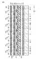
次に、図10を参照して、通常駆動時における表示動作及びタッチ検出動作について具体的に説明する。図10に示す例では、1ユニット表示ライン数(LINE_NUMBER_OF_UNIT)として45が設定されているものとする。なお、1フレームの画面を表示する表示動作の周期(つまり、1フレーム期間の各ユニットに含まれる表示期間DISにおいて画素信号が書き込まれたライン数)は、図10に示すユニット番号(Unit0、Unit1、…)で管理することができる。 Next, a display operation and a touch detection operation during normal driving will be specifically described with reference to FIG. In the example shown in FIG. 10, it is assumed that 45 is set as the number of display lines per unit (LINE_NUMBER_OF_UNIT). Note that the cycle of the display operation for displaying the screen of one frame (that is, the number of lines in which the pixel signal is written in the display period DIS included in each unit of one frame period) is the unit number (Unit0, Unit1) shown in FIG. , ...) can be managed.
図10に示す開始ライン及び終了ラインは、垂直バックポーチ期間BP、各ユニットに含まれる表示期間DIS及び垂直フロントポーチ期間FPの各々において駆動される最初のラインの位置及び最後のラインの位置を表している。また、図10に示すライン数は、垂直バックポーチ期間BP、各ユニットに含まれる表示期間DIS及び垂直フロントポーチ期間FPの各々において駆動されるライン数を表している。 The start line and the end line shown in FIG. 10 represent the position of the first line and the position of the last line driven in each of the vertical back porch period BP, the display period DIS included in each unit, and the vertical front porch period FP. ing. The number of lines shown in FIG. 10 represents the number of lines driven in each of the vertical back porch period BP, the display period DIS included in each unit, and the vertical front porch period FP.
ここでは、垂直バックポーチ期間BPにおいて4本のラインが駆動され、垂直フロントポーチ期間FPにおいて2本のラインが駆動される例が示されている。また、有効なアクティブ表示ライン数(表示動作によって画素信号が書き込まれるライン数)は、ユニット0〜ユニット42までの1920であるものとする。この場合、ユニット0〜ユニット41までのライン数はそれぞれ1ユニット表示ライン数として設定されている45であるが、ユニット42のライン数は端数としての30(=1920−45*41)である。以下、このユニット42はダミーユニットと称する。なお、図9においてダミーユニットはユニットn+3であり、当該ダミーユニットに含まれる表示期間は表示期間DIS´とする。 Here, an example is shown in which four lines are driven in the vertical back porch period BP and two lines are driven in the vertical front porch period FP. The number of effective active display lines (the number of lines in which pixel signals are written by the display operation) is assumed to be 1920 from
ここで、ダミーユニットに含まれる表示期間DIS´において駆動されるライン数(30)は他のユニット0〜ユニット42に含まれる表示期間DISにおいて駆動されるライン数(45)よりも少ないため、表示期間DIS´の長さは、表示期間DISよりも短い。また、ダミーユニットには、タッチ検出期間は含まれないものとする。なお、ダミーユニット以外のユニットのユニット番号の最大値は、有効ユニット番号(VALID_UNIT_NUM)と称する。図10に示す例では、有効ユニット番号は42である。なお、有効ユニット番号は予め設定されている。 Here, since the number (30) of lines driven in the display period DIS ′ included in the dummy unit is smaller than the number of lines (45) driven in the display period DIS included in the
なお、上記した垂直バックポーチ期間BP及び垂直フロントポーチ期間FPにおいて駆動されるラインの数は、例えば表示パネルPNLの仕様によって定められている。
ここで、タッチ検出期間Tは表示期間DISの後に配置されるため、当該タッチ検出期間Tの配置(タイミング)については上記したユニット番号で管理することができる。一方、上記したようにタッチ検出動作の周期が表示動作の周期と独立している場合には、タッチ検出動作の周期をユニット番号で管理することはできない。
このため、タッチ検出動作の周期は、ユニット(タッチ検出期間T)毎にインクリメントするように構成されたLOOPカウンタ(LOOP_CNT)を用いて管理されるものとする。Note that the number of lines driven in the vertical back porch period BP and the vertical front porch period FP is determined by, for example, the specifications of the display panel PNL.
Here, since the touch detection period T is arranged after the display period DIS, the arrangement (timing) of the touch detection period T can be managed by the unit number described above. On the other hand, when the touch detection operation cycle is independent of the display operation cycle as described above, the touch detection operation cycle cannot be managed by the unit number.
Therefore, it is assumed that the cycle of the touch detection operation is managed using a LOOP counter (LOOP_CNT) configured to be incremented for each unit (touch detection period T).
ここで、上記したタッチ検出動作の周期に対応するユニット数(以下、タッチ最大ユニット数と表記)は、予め設定されているものとする。このようなタッチ最大ユニット数(MAX_LOOP_NUM)が例えば29であるものとすると、0〜29の値を取り得るLOOPカウンタを利用することによってタッチ検出動作の周期を管理することができる。 Here, it is assumed that the number of units corresponding to the period of the touch detection operation described above (hereinafter referred to as the maximum number of touch units) is set in advance. If the maximum number of touch units (MAX_LOOP_NUM) is 29, for example, the period of the touch detection operation can be managed by using a LOOP counter that can take a value of 0 to 29.
具体的には、図10に示すようにLOOPカウンタ(値)は、ユニット0〜ユニット29まで順次インクリメントされ、ユニット30において0にリセットされ、ユニット31から再度インクリメントされる。これにより、タッチ検出動作(の周期)を表示動作と独立して管理することができる。 Specifically, as shown in FIG. 10, the LOOP counter (value) is sequentially incremented from
なお、図10に示すユニット41及びユニット42に示すように、LOOPカウンタはダミーユニット(ここでは、ユニット42)ではインクリメントされないものとする。これは、上記した有効ユニット番号が41に設定されており、ダミーユニットではタッチ検出期間が設定されていないからである。 As shown in the
また、LOOPカウンタは、垂直フロントポーチ期間FP及び垂直バックポーチ期間BP中はインクリメントされないが、垂直フロントポーチ期間FP及び垂直バックポーチ期間BP中も値を維持するものとする。これによれば、新たな垂直同期信号VSYNCが入力された後のユニット0(のタッチ検出期間)においては、垂直フロントポーチ期間FP及び垂直バックポーチ期間BP中に維持されていた値に対してインクリメントが再開される。以下、同様の動作が繰り返される。 The LOOP counter is not incremented during the vertical front porch period FP and the vertical back porch period BP, but maintains the value during the vertical front porch period FP and the vertical back porch period BP. According to this, in the unit 0 (the touch detection period) after the new vertical synchronization signal VSYNC is input, it is incremented with respect to the values maintained during the vertical front porch period FP and the vertical back porch period BP. Is resumed. Thereafter, the same operation is repeated.
なお、ここではタッチ検出動作の周期が表示動作の周期と独立している(非同期である)ことによりLOOPカウンタを用いる例について説明したが、当該タッチ検出動作の周期と表示動作の周期とが同期している場合には、LOOPカウンタを用いることなく当該タッチ検出動作の周期及び表示動作の周期の両方をユニット番号(ユニット数)で管理するようにしても構わない。 Although the example in which the LOOP counter is used because the touch detection operation cycle is independent (asynchronous) with the display operation cycle has been described here, the touch detection operation cycle and the display operation cycle are synchronized. In this case, both the cycle of the touch detection operation and the cycle of the display operation may be managed by the unit number (number of units) without using the LOOP counter.
ところで、表示装置DSPにおいては、通常駆動時の表示駆動周波数を下げることによって省電力化を図る(消費電力を低減させる)場合がある。具体的には、通常駆動時において表示装置DSPが例えば表示駆動周波数60Hzで駆動している場合において、当該表示装置DSPを表示駆動周波数30Hzで駆動させる場合がある。
以下、通常駆動時の表示駆動周波数を下げて表示装置DSPを駆動させることを低速駆動(低周波駆動)と称する。By the way, in the display device DSP, there are cases where power saving is achieved (power consumption is reduced) by lowering the display driving frequency during normal driving. Specifically, when the display device DSP is driven at a display drive frequency of 60 Hz, for example, during normal driving, the display device DSP may be driven at a display drive frequency of 30 Hz.
Hereinafter, driving the display device DSP by lowering the display driving frequency during normal driving is referred to as low speed driving (low frequency driving).
通常駆動及び低速駆動は、例えば上記したビデオメモリ103に書き込まれる画素データ等に基づいて、パネルドライバIC1(に備えられるタイミングコントローラ107)によって動的に切り替えられるものとする。具体的には、I/F回路101が周波数切替判定回路を有し、所定の条件に基づいて、周波数の切り替えを判定し、判定結果をタイミングコントローラ107等に送信するようにしてもよい。なお、所定の条件は、周波数の切り替え(つまり、通常駆動及び低速駆動間の切り替え)によって画質を低下させることがないような観点に基づいて設定されている。例えば、I/F回路101が画像解析回路を有し、表示装置DSP(の表示パネルPNL)においてホーム画面が表示、あるいは同じ写真が表示されている等の画面(画像)の書き換えが不要な場合かを判定し、不要な場合に低速駆動(低周波)への切替信号を送信してもよい。また、ホスト装置HOSからの画素データの更新の頻度に基づいて判定してもよい。例えば、ホスト装置HOSから一定期間画素データの更新が無い場合に、表示装置DSPを低速駆動に切り替えるようにしてもよい。I/F回路101からの低速駆動への切替信号の送信に応じて、パネルドライバIC1は、表示装置DSPの駆動状態を通常駆動から低速駆動に切り替える。
すなわち、本実施形態において、周波数切替判定回路(I/F回路101)は、表示動作の周波数を、通常駆動時の表示駆動周波数(第1周波数)と、当該通常駆動時の表示駆動周波数よりも遅い低速駆動時の表示駆動周波数(第2周波数)とのいずれかに切り替えるように構成されている。
なお、I/F回路101が周波数切替判定回路として機能する場合を例示したが、データ処理回路102とビデオメモリ103が共同して周波数切替判定回路として機能してもよい。The normal driving and the low-speed driving are assumed to be dynamically switched by the panel driver IC 1 (a
That is, in the present embodiment, the frequency switching determination circuit (I / F circuit 101) sets the display operation frequency to a display drive frequency (first frequency) during normal drive and a display drive frequency during normal drive. The display driving frequency (second frequency) at the time of slow low speed driving is switched to any one.
Although the case where the I /
なお、通常駆動及び低速駆動の切り替えは、例えばホスト装置HOSからのコマンドに従って実行されても構わない。
ここで、表示装置DSPを低速駆動させる場合、通常駆動時と比較して1フレーム期間が長くなる。本実施形態において、低速駆動時であっても各ユニットに含まれる表示期間DIS及びタッチ検出期間Tの長さは通常駆動時と同一とする構成を採用し、当該通常駆動時の1フレーム期間との差分については表示調整期間(ポーチ期間)を長くすることによって対応する。この場合、例えば、タイミングコントローラ107及び表示駆動回路108は、I/F回路101に含まれる周波数切替判定回路の判定結果に応じて、表示調整期間の長さを変更するように構成されたポーチ期間変更回路を有する。このポーチ期間変更回路は、周波数切替判定回路の判定結果が例えば低速駆動(低周波)への切り替えであった場合、当該判定結果を示す切替信号を周波数切替判定回路から受信し、低速駆動時における表示調整期間(ポーチ期間)を示す信号、例えば、ENABLE信号を出力する。Note that switching between normal driving and low-speed driving may be executed in accordance with a command from the host device HOS, for example.
Here, when the display device DSP is driven at a low speed, one frame period is longer than that during normal driving. In the present embodiment, a configuration is adopted in which the length of the display period DIS and the touch detection period T included in each unit is the same as that during normal driving even during low speed driving, and one frame period during normal driving. This difference is dealt with by lengthening the display adjustment period (pouch period). In this case, for example, the
このため、本実施形態においては、表示装置DSPにおいて、フレームの最初の画素行に画素データを書き始める時点と、フレームの最後の画素行に画素データを書き終える時点との差が、常に一定時間を保つことができる。なお、表示調整期間は、画像の表示の極性を反転する垂直バックポーチ期間BPと、垂直バックポーチ期間の前に設けられている垂直フロントポーチ期間FPとを含むが、低速駆動時にはいずれを長くしてもよい。本実施形態においては、垂直フロントポーチ期間FPを長くする(延長する)ものとする。 For this reason, in this embodiment, in the display device DSP, the difference between the time when the pixel data starts to be written in the first pixel row of the frame and the time when the pixel data finishes writing in the last pixel row of the frame is always constant time. Can keep. The display adjustment period includes a vertical back porch period BP that reverses the polarity of image display and a vertical front porch period FP that is provided before the vertical back porch period. May be. In the present embodiment, the vertical front porch period FP is lengthened (extended).
ここで、図11及び図12を参照して、上記した通常駆動時の垂直フロントポーチ期間FPを単に長くした場合における表示動作及びタッチ検出動作を本実施形態に対する比較例として説明する。
この比較例においては、図11に示すように、垂直バックポーチ期間BP及び各ユニット(表示期間DIS及びタッチ検出期間T)は図9に示す通常駆動時と同様であるが、垂直フロントポーチ期間FP´は、通常駆動時の垂直フロントポーチ期間FPと比較して長くなっている。Here, with reference to FIG. 11 and FIG. 12, a display operation and a touch detection operation in the case where the vertical front porch period FP during normal driving described above is simply extended will be described as a comparative example with respect to the present embodiment.
In this comparative example, as shown in FIG. 11, the vertical back porch period BP and each unit (display period DIS and touch detection period T) are the same as those in the normal driving shown in FIG. 'Is longer than the vertical front porch period FP during normal driving.
この場合、図12に示すように、垂直フロントポーチ期間FP´の開始ラインは図10に示す通常駆動時の垂直フロントポーチ期間FPと同様であるが、終了ラインは3846、ライン数は1922となっており、通常駆動時と比較して増大している。
なお、上記した最大表示ライン数は通常駆動時と低速駆動時とで変更されるものではない。すなわち、図12に示す垂直フロントポーチ期間FP´のライン数は、当該ライン数のラインが駆動されたことを表す数値ではなく、当該ライン数のラインが駆動されるのと同等の時間が垂直フロントポーチ期間FP´に割り当てられていることを表している。垂直フロントポーチ期間FP´の終了ラインについても同様に、開始ラインから終了ラインまでのラインが駆動されるのと同等の時間が垂直フロントポーチ期間FP´に割り当てられていることを示している。In this case, as shown in FIG. 12, the start line of the vertical front porch period FP ′ is the same as the vertical front porch period FP during normal driving shown in FIG. 10, but the end line is 3846 and the number of lines is 1922. And increased compared to normal driving.
The maximum number of display lines described above is not changed between normal driving and low speed driving. That is, the number of lines in the vertical front porch period FP ′ shown in FIG. 12 is not a numerical value indicating that the number of lines has been driven, but is equal to the time for driving the number of lines. It shows that it is assigned to the pouch period FP ′. Similarly, with respect to the end line of the vertical front porch period FP ′, it is indicated that the time equivalent to the driving of the line from the start line to the end line is allocated to the vertical front porch period FP ′.
ここで、上述した通常駆動時における垂直フロントポーチ期間FP´を長くした場合、図11に示すように当該垂直フロントポーチ期間FP´においては表示動作及びタッチ検出動作が実行されない(ブランキング期間)。
なお、垂直フロントポーチ期間FP´よりも前に1フレームの画像の表示動作は終了しているため、垂直フロントポーチ期間FP´中に表示動作は実行される必要はない。Here, when the vertical front porch period FP ′ during normal driving described above is lengthened, the display operation and the touch detection operation are not performed in the vertical front porch period FP ′ as shown in FIG. 11 (blanking period).
Note that the display operation of one frame image is completed before the vertical front porch period FP ′, and therefore it is not necessary to execute the display operation during the vertical front porch period FP ′.
しかしながら、垂直フロントポーチ期間FP´中にタッチ検出動作が実行されない場合には、当該垂直フロントポーチ期間FP´においてタッチ操作を検出することができないため、表示装置DSPにおけるタッチ検出感度が低下する。
そこで、本実施形態においては、パネルドライバIC1(に含まれるタイミングコントローラ107)による制御のもと、低速駆動時の1フレーム期間で表示装置DSPが動作する場合において垂直フロントポーチ期間がFP´に延長された場合、当該垂直フロントポーチ期間FP´に、駆動電極Tx(として動作する共通電極COME)を駆動してタッチ検出電極Rxがタッチ検出信号Rxsを出力するタッチ検出期間(第2のタッチ検出期間)を割り当てるものとする。なお、本実施形態においては、垂直フロントポーチ期間FP´にタッチ検出期間を割り当てるか否かを決定するLP_VFP_TP_ENBが予め設定されているものとする。このLP_VFP_TP_ENBは、例えばタイミングコントローラ107からタッチ駆動回路109に対して与えられるもので、タッチ駆動周波数切り替え指令として利用されている。この場合、例えば、タイミングコントローラ107及びタッチ駆動回路109は、I/F回路101に含まれる周波数切替判定回路の判定結果に応じて、表示調整期間において、タッチ駆動(タッチ検出動作)を実施するか否かを切り替えるように構成されたタッチ駆動切替回路を有する。周波数切替判定回路の判定結果が例えば低速駆動(低周波)への切り替えであった場合、タッチ駆動切替回路は、当該判定結果を示す切替信号を周波数切替判定回路から受信し、表示調整期間(ポーチ期間)中においてタッチ駆動を実施するための信号、例えば、VSHDまたはTSHD信号を出力する。なお、LP_VFP_TP_ENB=1であれば、低速駆動時の垂直フロントポーチ期間FP´にタッチ検出期間が割り当てられるものとする。一方、LP_VFP_TP_ENB=0とすることによって、低速駆動時の垂直フロントポーチ期間FP´にタッチ検出期間を割り当てない構成とすることも可能である。However, when the touch detection operation is not executed during the vertical front porch period FP ′, the touch operation cannot be detected during the vertical front porch period FP ′, and thus the touch detection sensitivity in the display device DSP decreases.
Therefore, in the present embodiment, the vertical front porch period is extended to FP ′ when the display device DSP operates in one frame period during low-speed driving under the control of the panel driver IC 1 (included in the timing controller 107). In this case, during the vertical front porch period FP ′, the touch detection electrode Rx outputs the touch detection signal Rxs by driving the drive electrode Tx (the common electrode COME that operates as the second touch detection period). ). In the present embodiment, it is assumed that LP_VFP_TP_ENB for determining whether or not to assign a touch detection period to the vertical front porch period FP ′ is set in advance. This LP_VFP_TP_ENB is given from the
以下、本実施形態に係る低速駆動時における表示装置DSPの表示動作及びタッチ検出動作について説明する。
図13を参照して、本実施形態での低速駆動時における表示期間及びタッチ検出期間の配置について説明する。
図13に示すようにパネルドライバIC1において表示用の垂直同期信号VSYNCが入力される(つまり、1フレーム期間が開始される)と、垂直バックポーチ期間BPを経て、表示動作及びタッチ検出動作が実行される。この場合、上記した通常駆動時と同様に、1フレーム期間においては、表示動作及びタッチ検出動作が繰り返し実行される(つまり、表示期間DIS及びタッチ検出期間Tが交互に配置されている)。Hereinafter, the display operation and the touch detection operation of the display device DSP during low-speed driving according to the present embodiment will be described.
With reference to FIG. 13, the arrangement of the display period and the touch detection period during low-speed driving in the present embodiment will be described.
As shown in FIG. 13, when the display vertical synchronization signal VSYNC is input to the panel driver IC 1 (that is, one frame period is started), the display operation and the touch detection operation are executed through the vertical back porch period BP. Is done. In this case, similarly to the above-described normal driving, the display operation and the touch detection operation are repeatedly executed in one frame period (that is, the display period DIS and the touch detection period T are alternately arranged).
ここで、図11示す最後のユニットn+3の後の垂直フロントポーチ期間FPにおいてはタッチ検出期間Tは設定されておらずブランキング期間となっているが、本実施形態においては、図13に示すようにユニットn+3と垂直フロントポーチ期間FP´を含む期間においては所定の間隔でタッチ検出期間T´が割り当てられている。なお、このタッチ検出期間T´が割り当てられる所定の間隔については後述する。 Here, in the vertical front porch period FP after the last unit n + 3 shown in FIG. 11, the touch detection period T is not set and is a blanking period, but in this embodiment, as shown in FIG. In the period including the unit n + 3 and the vertical front porch period FP ′, the touch detection period T ′ is assigned at a predetermined interval. The predetermined interval to which this touch detection period T ′ is assigned will be described later.
次に、図14を参照して、本実施形態での低速駆動時における表示動作及びタッチ検出動作について具体的に説明する。なお、上述した図10に示す通常駆動時と同様に、1ユニット表示ライン数として45が設定されているものとする。
また、図14に示す垂直バックポーチ期間BP及びユニット0〜ユニット41は、図10に示す垂直バックポーチ期間BP及びユニット0〜41と同様であるため、その詳しい説明を省略する。Next, with reference to FIG. 14, the display operation and the touch detection operation during low-speed driving in the present embodiment will be specifically described. It is assumed that 45 is set as the number of display lines per unit, as in the case of normal driving shown in FIG.
Further, the vertical back porch period BP and
ここで、図14に示すユニット42は、図10に示すユニット42(以下、通常駆動時のユニット42と表記)に相当する。しかしながら、図14に示すユニット42(以下、低速駆動時のユニット42と表記)は、当該通常駆動時のユニット42とは開始ライン、終了ライン及びライン数が異なる。これは、通常駆動時のユニット42にはユニット41までの表示期間において駆動されたラインの端数のライン(1ユニット表示ライン数よりも少ない数のライン)に対する表示動作(表示期間DIS´)が割り当てられているのに対して、低速駆動時のユニット42には、図13に示すように当該端数のラインに対する表示動作(表示期間DIS´)及びタッチ検出期間T´が割り当てられていることに起因する。 Here, the
更に、低速駆動時のユニット42に含まれる表示期間DIS´において駆動されるライン数は1ユニット表示ライン数よりも少ないため、当該表示期間DIS´は、1フレーム期間において当該ユニット42よりも前に設定されているユニット0〜ユニット41に含まれる表示期間DISよりも短い。このため、低速駆動時のユニット42においては、表示期間DIS´に対して所定のブランキング期間が付加されている。 Furthermore, since the number of lines driven in the display period DIS ′ included in the
なお、低速駆動時のユニット42に含まれる表示期間DIS´及び当該表示期間DIS´に付加されたブランキング期間の長さは、他のユニット0〜42に含まれる表示期間DISの長さと同一である。また、低速駆動時のダミーユニット42に含まれるタッチ検出期間T´の長さは、他のユニット0〜42に含まれるタッチ検出期間Tと同一である。 Note that the length of the display period DIS ′ included in the
これにより、低速駆動時のユニット42に含まれる表示期間DIS´、ブランキング期間及びタッチ検出期間T´の長さは、他のユニット0〜42に含まれる表示期間DIS及びタッチ検出期間Tと同一となる。
また、低速駆動時のユニット42(表示期間DIS´、ブランキング期間及びタッチ検出期間T´)の後には、低速駆動に対応するために延長された垂直フロントポーチ期間FP´が設定されている。本実施形態においては、この垂直フロントポーチ期間FP´中においても複数のユニット43〜85が設定されている。垂直フロントポーチ期間FP´中に設定されるユニット43〜84は、上記した表示期間DISと同等の長さのブランキング期間と、タッチ検出期間T´とを含む。すなわち、ユニット43〜85の各々(に含まれるブランキング期間及びタッチ検出期間T´)の長さは、他のユニット0〜42と同一である。Thereby, the length of the display period DIS ′, the blanking period, and the touch detection period T ′ included in the
Further, after the unit 42 (display period DIS ′, blanking period, and touch detection period T ′) at the time of low speed driving, a vertical front porch period FP ′ extended to correspond to low speed driving is set. In the present embodiment, a plurality of
これにより、本実施形態においては、垂直フロントポーチ期間FP´中においてもタッチ検出期間T´がタッチ検出期間Tと同一の間隔で配置され、ユニットの単位(ユニット番号)でタッチ検出期間T´の配置を管理することができる。なお、低速駆動時におけるタッチ検出動作の周期は、通常駆動時と同様に上述したLOOPカウンタを用いて管理される。 Accordingly, in the present embodiment, the touch detection period T ′ is arranged at the same interval as the touch detection period T even during the vertical front porch period FP ′, and the unit (unit number) of the touch detection period T ′ is arranged. The arrangement can be managed. Note that the cycle of the touch detection operation at the time of low speed driving is managed using the above-described LOOP counter as in the case of normal driving.
図14に示すユニット85は、低速駆動時の1フレーム期間を調整するために設けられており、例えばブランキング期間のみを含むユニットである。なお、図14に示す例では、低速駆動時の有効ユニット番号(LP_VALID_UNIT_NUM)として84が予め設定されている。 A
なお、図14に示すユニット42以降の各ユニットの開始ライン、終了ライン及びライン数については上記した図12の垂直フロントポーチ期間FP´に関して説明した通りであり、当該各ユニットには1ユニット表示ライン(ここでは、45)が駆動される表示期間に相当するブランキング期間及びタッチ検出期間T´が含まれていることを便宜的に示している。
次に、図15のフローチャートを参照して、本実施形態に係る表示装置DSPの駆動状態を切り替える際の当該表示装置DSPの処理手順の概要について簡単に説明する。ここでは、表示装置DSPの駆動状態が通常駆動であるものとする。
本実施形態において、上記したI/F回路101に含まれる周波数切替判定回路は、上記した所定の条件に基づいて、表示装置DSPの駆動状態を切り替えるか否かを判定する(ステップS1)。
なお、この所定の条件としては、例えば表示装置DSPの画面の書き換えが不要であるか否か等が含まれる。すなわち、上記したように表示装置DSPの駆動状態が通常駆動であるものとすると、表示装置DSPの画面の書き換えが不要である場合には、低速駆動としたとしても画質を低下させる等の影響が少ないため、表示装置DSPの駆動状態を切り替えると判定される。一方、表示装置DSPの画面の書き換えが不要でない場合には、低速駆動とした場合には画質の低下への影響が大きいため、表示装置DSPの駆動状態を切り替えないと判定される。
表示装置DSPの駆動状態を切り替えないと判定された場合(ステップS1のNO)、図15の処理は終了され、現在の駆動状態が維持された状態で、表示動作及びタッチ検出動作が実行される。
一方、表示装置DSPの駆動状態を切り替えると判定された場合(ステップS1のYES)、周波数切替判定回路は、当該判定結果を示す切替信号(つまり、駆動状態を切り替える旨の信号)をタイミングコントローラ107に送信する。
タイミングコントローラ107は、周波数切替判定回路によって送信された切替信号を受信する。タイミングコントローラ107において切替信号が受信されると、タイミングコントローラ107及び表示駆動回路108の共同によって実現されるポーチ期間変更回路は、現在の表示調整期間(の長さ)の設定を変更する(ステップS2)。ここでは、現在の通常駆動時における表示調整期間が、低速駆動時における表示調整期間に変更される(すなわち、表示調整期間が延長される)。この場合、ポーチ期間変更回路は、低速駆動時における表示調整期間を示す信号を表示パネルPNLに出力する。
更に、上記したようにタイミングコントローラ107において切替信号が受信されると、タイミングコントローラ107及びタッチ駆動回路109の共同によって実現されるタッチ駆動切替回路は、表示調整期間中のタッチ駆動(タッチ検出動作)の設定を変更する(ステップS3)。
ここで、表示装置DSPの駆動状態が通常駆動である場合には、上述したように表示調整期間中にタッチ検出動作は実行されない(つまり、表示調整期間中のタッチ駆動がOFFに設定されている)。したがって、ここでは表示調整期間中のタッチ駆動がONに変更される。この場合、タッチ駆動切替回路は、表示調整期間中においてタッチ検出動作を実行するための信号を表示パネルPNLに出力する。
表示パネルPNLにおいては、上記したステップS2及びS3において変更された設定(ポーチ期間変更回路及びタッチ駆動切替回路によって出力された信号)に基づき表示動作及びタッチ検出動作が実行(制御)される(ステップS4)。これにより、表示装置DSPの駆動状態を通常駆動から低速駆動に切り替えるとともに、当該低速駆動時における表示調整期間中にタッチ検出動作を実行することが可能となる。
ここでは、図15に示す処理が実行される時点の表示装置DSPの駆動状態が通常駆動である場合について説明したが、当該処理が実行される時点での表示装置DSPの駆動状態が低速駆動である場合についても同様である。
具体的には、表示装置DSPの駆動状態が低速駆動である場合において例えば表示装置DSPの画面の書き換えが必要である場合、ステップS1においては、表示装置DSPの駆動状態を切り替えると判定される。
この場合には、ステップS2において低速駆動時における表示調整期間(の設定)が通常駆動時における表示調整期間に変更され、ステップS3において表示調整期間中のタッチ駆動がOFFに変更される。また、ステップS4においては、このように変更された設定に基づいて表示動作及びタッチ検出動作が実行される(つまり、表示装置DSPの駆動状態が低速駆動から通常駆動に切り替えられる)。
なお、図15の処理(ステップS1の処理)は、定期的に実行されるものとする。これにより、本実施形態においては、表示装置DSPの駆動状態を動的に切り替えるとともに、当該駆動状態に応じた表示動作及びタッチ検出動作を実行することが可能となる。The start line, the end line, and the number of lines of each unit after the
Next, with reference to the flowchart of FIG. 15, an outline of a processing procedure of the display device DSP when the driving state of the display device DSP according to the present embodiment is switched will be briefly described. Here, it is assumed that the driving state of the display device DSP is normal driving.
In the present embodiment, the frequency switching determination circuit included in the I /
The predetermined condition includes, for example, whether or not the screen of the display device DSP needs to be rewritten. That is, as described above, if the display device DSP is driven normally, the screen of the display device DSP need not be rewritten. Since there are few, it determines with switching the drive state of the display apparatus DSP. On the other hand, when it is not necessary to rewrite the screen of the display device DSP, it is determined that the drive state of the display device DSP is not switched because low-speed driving has a large effect on the deterioration of image quality.
When it is determined that the drive state of the display device DSP is not switched (NO in step S1), the processing in FIG. 15 is terminated, and the display operation and the touch detection operation are executed in a state where the current drive state is maintained. .
On the other hand, when it is determined that the driving state of the display device DSP is to be switched (YES in step S1), the frequency switching determination circuit sends a switching signal indicating the determination result (that is, a signal for switching the driving state) to the
The
Further, as described above, when the switching signal is received by the
Here, when the drive state of the display device DSP is the normal drive, as described above, the touch detection operation is not performed during the display adjustment period (that is, the touch drive during the display adjustment period is set to OFF). ). Therefore, here, the touch drive during the display adjustment period is changed to ON. In this case, the touch drive switching circuit outputs a signal for executing the touch detection operation to the display panel PNL during the display adjustment period.
In the display panel PNL, the display operation and the touch detection operation are executed (controlled) based on the settings (signals output by the pouch period changing circuit and the touch drive switching circuit) changed in steps S2 and S3 described above (step). S4). As a result, the driving state of the display device DSP can be switched from the normal driving to the low speed driving, and the touch detection operation can be executed during the display adjustment period during the low speed driving.
Here, the case has been described where the display device DSP is driven in the normal driving state when the processing shown in FIG. 15 is executed, but the display device DSP is driven in the low speed driving state when the processing is executed. The same applies to certain cases.
Specifically, when the drive state of the display device DSP is low speed drive, for example, when the screen of the display device DSP needs to be rewritten, it is determined in step S1 that the drive state of the display device DSP is switched.
In this case, in step S2, the display adjustment period (setting) at the time of low speed driving is changed to the display adjustment period at the time of normal driving, and in step S3, the touch driving during the display adjustment period is changed to OFF. In step S4, the display operation and the touch detection operation are executed based on the settings changed in this way (that is, the drive state of the display device DSP is switched from the low speed drive to the normal drive).
Note that the process of FIG. 15 (the process of step S1) is executed periodically. Thereby, in the present embodiment, it is possible to dynamically switch the driving state of the display device DSP and to perform the display operation and the touch detection operation according to the driving state.
以下、本実施形態における表示動作及びタッチ検出動作に関する各種信号について簡単に説明する。
図16は、通常駆動時の表示動作及びタッチ検出動作に関する各種信号の関係を表すタイミングチャートである。図16においては便宜的にユニット等については簡略化されているが、1フレーム期間においては、垂直バックポーチ期間BP、各ユニットに含まれる表示期間DIS及びタッチ検出期間Tが交互に配置される期間及び垂直フロントポーチ期間FPが含まれている。Hereinafter, various signals related to the display operation and the touch detection operation in this embodiment will be briefly described.
FIG. 16 is a timing chart showing the relationship between various signals related to the display operation and the touch detection operation during normal driving. In FIG. 16, the units and the like are simplified for convenience, but in one frame period, the vertical back porch period BP, the display period DIS included in each unit, and the touch detection period T are alternately arranged. And a vertical front porch period FP.
図16においては、パネルドライバIC1の内部信号として、VSYNC、ENABLE、HSYNC及びDataが示されている。
VSYNCは、1フレーム期間(表示動作の周期)の開始を表す垂直同期信号(画像)である。ENABLEは、表示画素PXへの画素信号の書き込みが可能であることを示すイネーブル信号(画像)である。HSYNCは、1フレームの画面におけるライン毎の表示動作のタイミングを表す水平同期信号(画像)である。Dataは、ビデオメモリ103から読み出される画素データを表している。In FIG. 16, VSYNC, ENABLE, HSYNC, and Data are shown as internal signals of the panel driver IC1.
VSYNC is a vertical synchronization signal (image) representing the start of one frame period (display operation cycle). ENABLE is an enable signal (image) indicating that the pixel signal can be written to the display pixel PX. HSYNC is a horizontal synchronization signal (image) that represents the timing of the display operation for each line on the screen of one frame. Data represents pixel data read from the
図16に示すパネルドライバIC1の内部信号によれば、VSYNCが入力された所定期間経過後にイネーブル信号がハイレベルとなり、1フレーム期間中の各表示期間DISにおいて、水平同期信号に基づいてビデオメモリ103から画素データが読み込まれることが示されている。 According to the internal signal of the panel driver IC1 shown in FIG. 16, the enable signal becomes a high level after a predetermined period of time when VSYNC is input, and the
また、図16には、表示パネルPNLに入力される信号(パネル信号)として、VST、VCK、Sn、ASW、SDST及びSDCKが示されている。
VSTはゲート回路スタートパルス(画像)であり、VCKはゲート回路シフトクロック(画像)である。なお、VST及びVCKは、表示パネルPNLに備えられるゲートドライバGDを制御するための信号である。Snは、ソース出力であり、パネルドライバIC1から表示パネルPNLに入力され、信号線Sを介して表示画素PXに書き込まれる画素信号を表している。ASWは、マルチプレクサ制御スイッチであり、例えばRGBを選択する信号を表している。SDSTはタッチ検出スタートパルス、SDCKはタッチ検出クロックである。SDST及びSDCKは、上述したようにタッチ検出に関する制御信号である。FIG. 16 shows VST, VCK, Sn, ASW, SDST, and SDCK as signals (panel signals) input to the display panel PNL.
VST is a gate circuit start pulse (image), and VCK is a gate circuit shift clock (image). VST and VCK are signals for controlling the gate driver GD provided in the display panel PNL. Sn is a source output, and represents a pixel signal input to the display panel PNL from the panel driver IC1 and written to the display pixel PX via the signal line S. ASW is a multiplexer control switch and represents, for example, a signal for selecting RGB. SDST is a touch detection start pulse, and SDCK is a touch detection clock. SDST and SDCK are control signals related to touch detection as described above.
このようなパネル信号(VST、VCK、Sn及びASW)が図16に示すようなタイミングで表示パネルPNLに入力されることによって、各表示期間DISにおいて、上記した水平同期信号に同期して1ユニット表示ラインに対応する表示画素PXが駆動される(当該表示画素PXに画素信号が書き込まれる)ことが示されている。一方、SDSTは上記したタッチ検出動作の周期の開始を示しており、図16に示す例では、1フレーム期間に2周期分のタッチ検出動作が実行される例を示している。また、SDCKは、各ユニットに含まれるタッチ検出期間Tの配置に応じて入力される。このようなSDST及びSDCKによれば、当該SDST及びSDCKによって選択される駆動電極Tx(共通電極COME)が各タッチ検出期間Tにおいて駆動されることが示されている。 When such panel signals (VST, VCK, Sn, and ASW) are input to the display panel PNL at the timing shown in FIG. 16, one unit is synchronized with the horizontal synchronization signal in each display period DIS. It is shown that the display pixel PX corresponding to the display line is driven (a pixel signal is written to the display pixel PX). On the other hand, SDST indicates the start of the cycle of the touch detection operation described above, and in the example illustrated in FIG. 16, the touch detection operation for two cycles is performed in one frame period. The SDCK is input according to the arrangement of the touch detection period T included in each unit. According to such SDST and SDCK, it is shown that the drive electrode Tx (common electrode COME) selected by the SDST and SDCK is driven in each touch detection period T.
更に、図16には、タッチドライバIC2に入力される信号(TPIC I/F)として、TSVD及びTSHDが示されている。TSVD及びTSHDは、パネルドライバIC1とタッチドライバIC2との同期をとるための信号(垂直同期信号及び水平同期信号)である。TSVDは、上記したタッチ検出動作の周期の開始に応じて入力される。また、TSHDは、各ユニットに含まれるタッチ検出期間Tに対応するように入力されている。 Further, FIG. 16 shows TSVD and TSHD as signals (TPIC I / F) input to the touch driver IC2. TSVD and TSHD are signals (vertical synchronization signal and horizontal synchronization signal) for synchronizing the panel driver IC1 and the touch driver IC2. TSVD is input in response to the start of the period of the touch detection operation described above. The TSHD is input so as to correspond to the touch detection period T included in each unit.
タッチドライバIC2は、図16に示すようなタイミングで入力されるTSVD及びTSHDに基づいて、タッチ検出期間Tにおいてタッチ検出電極Rxから出力されたタッチ検出信号からタッチ位置を検出することができる。
また、図16には、ホスト装置HOSに入力される信号(HOST I/F)として、TEが示されている。TEは、パネルドライバIC1からホスト装置HOSに入力されるVSYNC信号(マスタ同期信号)である。なお、図示されていないが、タッチドライバIC2によって検出されたタッチ位置は、ホスト装置HOSに出力される。表示装置DSPにおいては、VSCYNC信号(マスタ同期信号)、上記したTSVD及びTSHD等を用いることによって、パネルドライバIC1、タッチドライバIC2及びホスト装置HOS間で同期した動作が実現される。The
In FIG. 16, TE is shown as a signal (HOST I / F) input to the host device HOS. TE is a VSYNC signal (master synchronization signal) input from the panel driver IC1 to the host device HOS. Although not shown, the touch position detected by the
図17は、本実施形態における低速駆動時の表示動作及びタッチ検出動作に関する各種信号の関係を表すタイミングチャートである。一方、図18は、上述した比較例における低速駆動時の表示動作及びタッチ検出動作に関する各種信号の関係を表すタイミングチャートである。なお、ここでは図16と同様の部分については、その詳しい説明を省略する。 FIG. 17 is a timing chart showing the relationship between various signals relating to the display operation and the touch detection operation during low-speed driving in the present embodiment. On the other hand, FIG. 18 is a timing chart showing the relationship between various signals related to the display operation and the touch detection operation during low-speed driving in the comparative example described above. Here, detailed description of the same parts as those in FIG. 16 is omitted.
図17に示すように、本実施形態における低速駆動時においては、図18と比較して、垂直フロントポーチ期間FP´にタッチ検出期間T´が設定されている。具体的には、垂直フロントポーチ期間FP´においては、パネル信号としてSDST及びSDCKが表示パネルPNLに入力されており、TSVD及びTSHDがタッチドライバIC2に入力されている。
これにより、本実施形態においては、低速駆動によって延長された垂直フロントポーチ期間FP´にタッチ検出期間Tと同一の間隔で配置されたタッチ検出期間T´においてもタッチ検出動作が実行される。As shown in FIG. 17, at the time of low speed driving in the present embodiment, a touch detection period T ′ is set in the vertical front porch period FP ′ as compared with FIG. Specifically, in the vertical front porch period FP ′, SDST and SDCK are input to the display panel PNL as panel signals, and TSVD and TSHD are input to the touch driver IC2.
Thereby, in the present embodiment, the touch detection operation is also performed in the touch detection period T ′ arranged at the same interval as the touch detection period T in the vertical front porch period FP ′ extended by low-speed driving.
上記したように本実施形態においては、通常駆動時の1フレーム期間(第1の1フレーム期間)よりも長い1フレーム期間(第2の1フレーム期間)で低速駆動する場合に垂直フロントポーチ期間FP(表示調整期間)が垂直フロントポーチ期間FP´に延長され、当該垂直フロントポーチ期間FP´にタッチ検出期間T´(第2のタッチ検出期間)が割り当てられる。 As described above, in the present embodiment, the vertical front porch period FP is used when driving at low speed in one frame period (second one frame period) longer than one frame period (first one frame period) during normal driving. The (display adjustment period) is extended to the vertical front porch period FP ′, and the touch detection period T ′ (second touch detection period) is assigned to the vertical front porch period FP ′.
本実施形態においては、このような構成により、通常駆動時と比較して低速駆動時の垂直フロントポーチ期間FP´が長期間となる場合であっても、当該垂直フロントポーチ期間FP´においてタッチ操作を検出することが可能となる。すなわち、本実施形態においては、表示装置DSPを低速駆動させることによって消費電力を低減させることができるとともに、低速駆動時であってもタッチ検出感度の低下を抑制することが可能となる。 In the present embodiment, with such a configuration, even when the vertical front porch period FP ′ during low-speed driving is longer than that during normal driving, the touch operation is performed during the vertical front porch period FP ′. Can be detected. That is, in the present embodiment, power consumption can be reduced by driving the display device DSP at a low speed, and a decrease in touch detection sensitivity can be suppressed even during low-speed driving.
また、本実施形態において、低速駆動時の1フレーム期間に含まれる表示期間DIS及びタッチ検出期間Tの長さは、通常駆動時の1フレーム期間に含まれる表示期間DIS及びタッチ検出期間Tの長さと同一である。本実施形態においては、このような構成により、通常駆動時の画質を維持したまま表示装置DSPを低速駆動させることが可能となる。また、通常駆動時と低速駆動時で表示動作を変える必要がないため、当該表示動作に関する制御を簡易化することが可能である。 In the present embodiment, the length of the display period DIS and the touch detection period T included in one frame period during low-speed driving is equal to the length of the display period DIS and the touch detection period T included in one frame period during normal driving. Is the same. In the present embodiment, such a configuration makes it possible to drive the display device DSP at a low speed while maintaining the image quality during normal driving. In addition, since there is no need to change the display operation between normal driving and low-speed driving, it is possible to simplify the control related to the display operation.
また、本実施形態においては、ビデオメモリ103に書き込まれた画素データに基づいて、例えば画像の書き換えが不要である場合に通常駆動(第1の1フレーム期間)を低速駆動(第2の1フレーム期間)に動的に切り替えることが可能である。本実施形態においては、このように動的に低速駆動に切り替えることにより、省電力化を図ることができる。 Further, in this embodiment, based on the pixel data written in the
更に、本実施形態においては、表示期間DIS及びタッチ検出期間Tが1フレーム期間に交互に配置されており、低速駆動時の1フレーム期間の垂直フロントポーチ期間FP´に割り当てられるタッチ検出期間T´は、タッチ検出期間Tと同一の長さを有し、当該タッチ検出期間Tと同一の間隔で配置される。本実施形態においては、このような構成により、通常駆動時のタッチ検出動作の周期(タッチ駆動の駆動周波数)を一定に維持したまま表示装置DSPを低速駆動させることが可能となる。 Further, in the present embodiment, the display period DIS and the touch detection period T are alternately arranged in one frame period, and the touch detection period T ′ assigned to the vertical front porch period FP ′ of one frame period during low-speed driving. Has the same length as the touch detection period T and is arranged at the same interval as the touch detection period T. In this embodiment, such a configuration makes it possible to drive the display device DSP at a low speed while maintaining a constant period of touch detection operation during normal driving (drive frequency of touch driving).
また、本実施形態においては、タッチ検出動作(タッチ駆動動作)の周期を表示動作の周期と独立して制御(管理)する構成により、例えば低速駆動時におけるタッチ検出感度を向上させるようにタッチ検出動作を設定すること等が可能となる。
また、本実施形態においては、表示用の共通電極(表示期間に表示駆動電圧が印加される複数の共通電極)がタッチ検出用の駆動電極(タッチ駆動電圧が印加される複数の駆動電極)として用いられる構成により、表示装置DSPの薄型化及び画質の向上を実現することができる。In the present embodiment, the touch detection operation (touch drive operation) cycle is controlled (managed) independently of the display operation cycle, for example, touch detection so as to improve touch detection sensitivity during low-speed drive. It is possible to set the operation.
In the present embodiment, the display common electrode (the plurality of common electrodes to which the display drive voltage is applied during the display period) is used as the touch detection drive electrode (the plurality of drive electrodes to which the touch drive voltage is applied). Depending on the configuration used, it is possible to reduce the thickness of the display device DSP and improve the image quality.
更に、本実施形態においては、低速駆動時に延長された垂直フロントポーチ期間FP´にタッチ検出期間T´が割り当てられる構成により、極性反転を行った後、画像が書き込まれるまでの時間を一定にすることができる。なお、例えば低速駆動時に垂直バックポーチ期間BPを延長し、当該延長された垂直バックポーチ期間BPにタッチ検出期間T´が割り当てられる構成としてもよい。 Further, in the present embodiment, the touch detection period T ′ is assigned to the vertical front porch period FP ′ extended during low-speed driving, so that the time until the image is written after polarity inversion is made constant. be able to. For example, the vertical back porch period BP may be extended during low-speed driving, and the touch detection period T ′ may be assigned to the extended vertical back porch period BP.
なお、本実施形態においては共通電極COMEが走査線Gに沿って配置される場合について説明したが、本実施形態は、例えば共通電極COMEが信号線Sに沿って配置される表示装置DSPに適用されても構わない。また、本実施形態は、1フレーム期間に表示期間、タッチ検出期間及び表示調整期間が含まれており、低速駆動時等において当該表示調整期間が延長されるものであれば適用可能である。すなわち、本実施形態は、共通電極COMEの形状等に限定されるものではなく、例えば表示画素毎に(つまり、ブロック状の)共通電極が配置されるような構成に適用されても構わない。更に、タッチ検出機構SEは、駆動電極と検出電極を備える相互容量検出方式を示したが、自己容量検出方式のものでもよい。自己容量検出方式は、例えば複数の共通電極がマトリクス状に配列されて、各共通電極に対するタッチと非タッチにおいて電極容量が変化することを検出する方式である。また、本実施形態においてはインセル型と称されるタッチ検出機構SEを備える表示装置DSPについて説明したが、本実施形態は、例えばオンセル型のタッチ検出機構を備える表示装置DSPについて適用されても構わない。更に、本実施形態に係る表示パネルPNLは、バックライトを備える透過型の液晶表示装置を説明したが、上記したように、反射型等の液晶表示装置でもよいし、更に液晶層を用いたものに限られず、例えば有機ELパネル等を用いたものであってもよい。有機ELパネルにおいては、上記の共通電極COMEは、複数の有機EL素子の画素電極と有機発光層を介して対向し、駆動電極を構成してもよい。 In the present embodiment, the case where the common electrode COME is disposed along the scanning line G has been described. However, the present embodiment is applied to, for example, a display device DSP in which the common electrode COME is disposed along the signal line S. It does not matter. In addition, the present embodiment is applicable as long as the display period, the touch detection period, and the display adjustment period are included in one frame period, and the display adjustment period is extended during low-speed driving or the like. In other words, the present embodiment is not limited to the shape of the common electrode COME, and may be applied to a configuration in which a common electrode is arranged for each display pixel (that is, a block shape). Furthermore, although the touch detection mechanism SE has shown the mutual capacitance detection system including the drive electrode and the detection electrode, it may be of the self-capacitance detection system. The self-capacitance detection method is a method in which, for example, a plurality of common electrodes are arranged in a matrix and a change in electrode capacitance is detected between touching and non-touching each common electrode. Further, in the present embodiment, the display device DSP including the touch detection mechanism SE referred to as an in-cell type has been described. However, the present embodiment may be applied to, for example, a display device DSP including an on-cell type touch detection mechanism. Absent. Furthermore, the display panel PNL according to the present embodiment has been described as a transmissive liquid crystal display device having a backlight. However, as described above, a reflective liquid crystal display device may be used, or a liquid crystal layer may be used. For example, an organic EL panel or the like may be used. In the organic EL panel, the common electrode COME may be opposed to the pixel electrodes of the plurality of organic EL elements via the organic light emitting layer to constitute a drive electrode.
また、本実施形態に係る表示装置DSP(タッチ検出機能付き表示装置)は、各種電子機器に組み込まれて使用されても構わない。表示装置DSPが組み込まれる電子機器には、例えばテレビジョン装置、デジタルカメラ、ビデオカメラ、ノートブック型パーソナルコンピュータ、タブレットコンピュータ及びスマートフォン(携帯電話)、車載用ディスプレイ等が含まれる。本実施形態に係る表示装置DSPは、画像(映像)を表示する様々な分野の電子機器に組み込み可能である。 In addition, the display device DSP (display device with a touch detection function) according to the present embodiment may be used by being incorporated in various electronic devices. Electronic devices in which the display device DSP is incorporated include, for example, a television device, a digital camera, a video camera, a notebook personal computer, a tablet computer, a smartphone (mobile phone), an in-vehicle display, and the like. The display device DSP according to the present embodiment can be incorporated into electronic devices in various fields that display images (video).
なお、本願発明は、上記実施形態そのままに限定されるものではなく、実施段階ではその要旨を逸脱しない範囲で構成要素を変形して具体化できる。また、上記実施形態に開示されている複数の構成要素の適宜な組合せにより種々の発明を形成できる。例えば、実施形態に示される全構成要素から幾つかの構成要素を削除してもよい。更に、異なる実施形態に亘る構成要素を適宜組合せてもよい。 Note that the present invention is not limited to the above-described embodiment as it is, and can be embodied by modifying the constituent elements without departing from the scope of the invention in the implementation stage. Moreover, various inventions can be formed by appropriately combining a plurality of constituent elements disclosed in the embodiment. For example, some components may be deleted from all the components shown in the embodiment. Furthermore, constituent elements over different embodiments may be appropriately combined.
DSP…タッチ検出機能付き表示装置、PNL…表示パネル(表示部)、SE…タッチ検出機構(検出部)、IC1…パネルドライバ(制御部)、IC2…タッチドライバ、Rx…タッチ検出電極、HOS…ホスト装置、GD…ゲートドライバ、SD…ソースドライバ、CD…共通電極ドライバ、PX…表示画素(表示素子)、COME…共通電極(駆動電極)、101…I/F回路、102…データ処理回路、103…ビデオメモリ、104…表示用ラインデータラッチ回路、105…ソース増幅器、106…内部発振器、107…タイミングコントローラ、108…表示駆動回路、109…タッチ駆動回路、201…シフトレジスタ回路、202…選択回路、203…切替回路。 DSP ... Display device with touch detection function, PNL ... Display panel (display unit), SE ... Touch detection mechanism (detection unit), IC1 ... Panel driver (control unit), IC2 ... Touch driver, Rx ... Touch detection electrode, HOS ... Host device, GD ... gate driver, SD ... source driver, CD ... common electrode driver, PX ... display pixel (display element), COME ... common electrode (drive electrode), 101 ... I / F circuit, 102 ... data processing circuit, DESCRIPTION OF
Claims (16)
Translated fromJapanese前記表示動作が行われる表示期間とは異なる第1のタッチ検出期間において、外部近接物体に応じた検出信号を検出するためのタッチ検出動作を行う検出部と、
前記表示動作及び前記タッチ検出動作を制御する制御部と
を具備し、
前記表示動作によって1フレームの画像が表示される1フレーム期間は、前記表示期間、前記第1のタッチ検出期間及び前記画像の表示を調整するための表示調整期間を含み、
前記制御部は、通常駆動時の第1の1フレーム期間よりも長い第2の1フレーム期間で低速駆動する場合に前記表示調整期間を延長し、当該延長された表示調整期間に前記タッチ検出動作が行われる第2のタッチ検出期間を割り当てる
タッチ検出機能付き表示装置。A display unit that performs a display operation for displaying an image based on a pixel signal;
A detection unit that performs a touch detection operation for detecting a detection signal according to an external proximity object in a first touch detection period different from a display period in which the display operation is performed;
A control unit for controlling the display operation and the touch detection operation,
One frame period in which an image of one frame is displayed by the display operation includes the display period, the first touch detection period, and a display adjustment period for adjusting the display of the image,
The control unit extends the display adjustment period when driving at low speed in a second one frame period longer than the first one frame period in normal driving, and the touch detection operation is performed in the extended display adjustment period. A display device with a touch detection function that allocates a second touch detection period during which touch detection is performed.
前記表示部は、前記メモリに書き込まれた画素データから生成される画素信号に基づいて表示動作を行い、
前記制御部は、前記メモリに書き込まれる画素データに基づいて前記第1の1フレーム期間と前記第2の1フレーム期間とを切り替える
請求項3記載のタッチ検出機能付き表示装置。It has a memory to which pixel data is written from the outside,
The display unit performs a display operation based on a pixel signal generated from pixel data written in the memory,
The display unit with a touch detection function according to claim 3, wherein the control unit switches between the first one frame period and the second one frame period based on pixel data written in the memory.
前記制御部は、前記第1のタッチ検出期間と同一の長さの前記第2のタッチ検出期間を、前記第1のタッチ検出期間と同一の間隔で前記表示調整期間に割り当てる
請求項1記載のタッチ検出機能付き表示装置。The display period and the first touch detection period are alternately arranged in the second one frame period,
The said control part allocates the said 2nd touch detection period of the same length as the said 1st touch detection period to the said display adjustment period at the same space | interval as the said 1st touch detection period. Display device with touch detection function.
前記制御部は、前記複数の駆動電極にタッチ駆動電圧を印加する周期を前記1フレームの画像が表示される周期と独立して制御する
請求項1記載のタッチ検出機能付き表示装置。The detection unit includes a plurality of drive electrodes to which a touch drive voltage is applied in the first and second touch detection periods,
The display device with a touch detection function according to claim 1, wherein the control unit controls a cycle in which a touch drive voltage is applied to the plurality of drive electrodes independently of a cycle in which the image of one frame is displayed.
前記複数の共通電極は、前記複数の駆動電極として用いられる
請求項6記載のタッチ検出機能付き表示装置。The display unit includes a plurality of common electrodes to which a display driving voltage is applied during the display period,
The display device with a touch detection function according to claim 6, wherein the plurality of common electrodes are used as the plurality of drive electrodes.
前記制御部は、前記低速駆動する場合、前記垂直フロントポーチ期間を延長し、当該延長された垂直フロントポーチ期間に前記第2のタッチ検出期間を割り当てる
請求項1記載のタッチ検出機能付き表示装置。The display adjustment period includes a vertical back porch period for inverting the polarity of display of the image and a vertical front porch period provided before the vertical back porch period,
The display device with a touch detection function according to claim 1, wherein, when the low-speed driving is performed, the control unit extends the vertical front porch period and allocates the second touch detection period to the extended vertical front porch period.
前記表示動作が行われる表示期間とは異なる第1のタッチ検出期間において、外部近接物体に応じた検出信号を検出するためのタッチ検出動作を行うステップと、
前記表示動作及び前記タッチ検出動作を制御するステップと
を備え、
前記表示動作によって1フレームの画像が表示される1フレーム期間は、前記表示期間、前記第1のタッチ検出期間及び前記画像の表示を調整するための表示調整期間を含み、
前記制御するステップは、
通常駆動時の第1の1フレーム期間よりも長い第2の1フレーム期間で低速駆動する場合に前記表示調整期間を延長するステップと、
前記延長された表示調整期間に前記タッチ検出動作が行われる第2のタッチ検出期間を割り当てるステップと
を具備するタッチ検出方法。Performing a display operation for displaying an image based on the pixel signal;
Performing a touch detection operation for detecting a detection signal according to an external proximity object in a first touch detection period different from a display period in which the display operation is performed;
Controlling the display operation and the touch detection operation,
One frame period in which an image of one frame is displayed by the display operation includes the display period, the first touch detection period, and a display adjustment period for adjusting the display of the image,
The controlling step includes
Extending the display adjustment period when driving at low speed in a second one frame period longer than the first one frame period in normal driving;
Allocating a second touch detection period during which the touch detection operation is performed during the extended display adjustment period.
前記割り当てるステップにおいて、前記第1の1フレーム期間で通常駆動する場合には、当該第1の1フレーム期間に含まれる表示調整期間に前記第2のタッチ検出期間を割り当てない
を含む、請求項9記載のタッチ検出方法。Switching between the first one frame period and the second one frame period;
The assigning step includes not assigning the second touch detection period to a display adjustment period included in the first one frame period in the case of normal driving in the first one frame period. The touch detection method described.
前記表示動作を行うステップにおいて、前記メモリに書き込まれた画素データから生成される画素信号に基づいて表示動作を行い、
前記切り替えるステップにおいて、前記メモリに書き込まれる画素データに基づいて前記第1の1フレーム期間と前記第2の1フレーム期間とを切り替える
請求項11記載のタッチ検出方法。Writing external pixel data into the memory,
In the step of performing the display operation, the display operation is performed based on a pixel signal generated from the pixel data written in the memory,
The touch detection method according to claim 11, wherein in the switching step, the first one frame period and the second one frame period are switched based on pixel data written in the memory.
前記割り当てるステップにおいて、前記第1のタッチ検出期間と同一の長さの前記第2のタッチ検出期間を、前記第1のタッチ検出期間と同一の間隔で前記表示調整期間に割り当てる
請求項9記載のタッチ検出方法。The display period and the first touch detection period are alternately arranged in the second one frame period,
10. The assigning step, wherein the second touch detection period having the same length as the first touch detection period is assigned to the display adjustment period at the same interval as the first touch detection period. Touch detection method.
前記延長するステップにおいて、前記低速駆動する場合に前記垂直フロントポーチ期間を延長し、
前記割り当てるステップにおいて、前記延長された垂直フロントポーチ期間に前記第2のタッチ検出期間を割り当てる
請求項9記載のタッチ検出方法。The display adjustment period includes a vertical back porch period for inverting the polarity of display of the image and a vertical front porch period provided before the vertical back porch period,
In the extending step, extending the vertical front porch period when driving at a low speed,
The touch detection method according to claim 9, wherein in the assigning step, the second touch detection period is assigned to the extended vertical front porch period.
Priority Applications (2)
| Application Number | Priority Date | Filing Date | Title |
|---|---|---|---|
| JP2016196510AJP2018060319A (en) | 2016-10-04 | 2016-10-04 | Display device with touch detection function and touch detection method |
| US15/724,623US10739884B2 (en) | 2016-10-04 | 2017-10-04 | Display device having touch detection function and method |
Applications Claiming Priority (1)
| Application Number | Priority Date | Filing Date | Title |
|---|---|---|---|
| JP2016196510AJP2018060319A (en) | 2016-10-04 | 2016-10-04 | Display device with touch detection function and touch detection method |
Publications (1)
| Publication Number | Publication Date |
|---|---|
| JP2018060319Atrue JP2018060319A (en) | 2018-04-12 |
Family
ID=61758763
Family Applications (1)
| Application Number | Title | Priority Date | Filing Date |
|---|---|---|---|
| JP2016196510APendingJP2018060319A (en) | 2016-10-04 | 2016-10-04 | Display device with touch detection function and touch detection method |
Country Status (2)
| Country | Link |
|---|---|
| US (1) | US10739884B2 (en) |
| JP (1) | JP2018060319A (en) |
Cited By (3)
| Publication number | Priority date | Publication date | Assignee | Title |
|---|---|---|---|---|
| JP2020154480A (en)* | 2019-03-18 | 2020-09-24 | 株式会社ジャパンディスプレイ | Display device and display method |
| JP2021103289A (en)* | 2019-11-19 | 2021-07-15 | シナプティクス インコーポレイテッド | Device and method for proximity detection for display panel |
| WO2023017349A1 (en)* | 2021-08-10 | 2023-02-16 | 株式会社半導体エネルギー研究所 | Display device, display module, and electronic equipment |
Families Citing this family (8)
| Publication number | Priority date | Publication date | Assignee | Title |
|---|---|---|---|---|
| WO2018073690A1 (en) | 2016-10-21 | 2018-04-26 | Semiconductor Energy Laboratory Co., Ltd. | Touch sensor, display device, display module, and electronic device |
| US10304393B2 (en)* | 2017-08-21 | 2019-05-28 | Novatek Microelectronics Corp. | Brightness compensation method and circuit |
| WO2019178847A1 (en)* | 2018-03-23 | 2019-09-26 | 深圳市柔宇科技有限公司 | Touch display driving method and touch display screen |
| KR102605378B1 (en)* | 2018-07-19 | 2023-11-24 | 엘지디스플레이 주식회사 | Display apparatus with touch sensor |
| US11423685B2 (en)* | 2019-04-09 | 2022-08-23 | Novatek Microelectronics Corp. | Driving apparatus and operation method thereof |
| KR102614894B1 (en)* | 2019-05-02 | 2023-12-19 | 삼성디스플레이 주식회사 | Display apparatus and method of driving the same |
| KR102619961B1 (en)* | 2019-10-28 | 2024-01-02 | 엘지디스플레이 주식회사 | Touch circuit, touch display device, and touch driving method thereof |
| US11360628B2 (en)* | 2020-06-23 | 2022-06-14 | Wuhan China Star Optoelectronics Semiconductor Display Technology Co., Ltd. | Self-capacitive touch substrate and display device |
Family Cites Families (4)
| Publication number | Priority date | Publication date | Assignee | Title |
|---|---|---|---|---|
| JP5925896B2 (en)* | 2011-09-07 | 2016-05-25 | シナプティクス インコーポレイテッド | Capacitive detection during hidden update time |
| US9036084B2 (en)* | 2013-04-11 | 2015-05-19 | Qualcomm Incorporated | Apparatus and method for synchronous display of video data |
| JP2015201175A (en) | 2014-03-31 | 2015-11-12 | 株式会社ジャパンディスプレイ | Touch drive device, touch detection device and display device with touch detection function |
| US9870087B2 (en)* | 2015-05-27 | 2018-01-16 | Novatek Microelectronics Corp. | Display driving apparatus and method for driving touch display panel |
- 2016
- 2016-10-04JPJP2016196510Apatent/JP2018060319A/enactivePending
- 2017
- 2017-10-04USUS15/724,623patent/US10739884B2/enactiveActive
Cited By (8)
| Publication number | Priority date | Publication date | Assignee | Title |
|---|---|---|---|---|
| JP2020154480A (en)* | 2019-03-18 | 2020-09-24 | 株式会社ジャパンディスプレイ | Display device and display method |
| US11068107B2 (en) | 2019-03-18 | 2021-07-20 | Japan Display Inc. | Display device and display method |
| JP7203650B2 (en) | 2019-03-18 | 2023-01-13 | 株式会社ジャパンディスプレイ | Display device and display method |
| JP2021103289A (en)* | 2019-11-19 | 2021-07-15 | シナプティクス インコーポレイテッド | Device and method for proximity detection for display panel |
| JP7573404B2 (en) | 2019-11-19 | 2024-10-25 | シナプティクス インコーポレイテッド | Apparatus and method for proximity detection for a display panel - Patents.com |
| WO2023017349A1 (en)* | 2021-08-10 | 2023-02-16 | 株式会社半導体エネルギー研究所 | Display device, display module, and electronic equipment |
| JPWO2023017349A1 (en)* | 2021-08-10 | 2023-02-16 | ||
| JP7747755B2 (en) | 2021-08-10 | 2025-10-01 | 株式会社半導体エネルギー研究所 | Display device, display module and electronic device |
Also Published As
| Publication number | Publication date |
|---|---|
| US20180095575A1 (en) | 2018-04-05 |
| US10739884B2 (en) | 2020-08-11 |
Similar Documents
| Publication | Publication Date | Title |
|---|---|---|
| US10739884B2 (en) | Display device having touch detection function and method | |
| US11402935B2 (en) | Display device | |
| CN105224156B (en) | Display device and its driving method with integrated touch panels | |
| US9830025B2 (en) | Integrated touch display device for displaying image and performing touch sensing through time-divisional multiplexing | |
| US8952913B2 (en) | Display device and driving method thereof | |
| CN103049126B (en) | Display unit, display method and electronic system | |
| US10429993B2 (en) | Touch display driving integrated circuit and operation method thereof | |
| CN105353935B (en) | Display unit and electronic unit with touch detection function | |
| US10175791B2 (en) | Display device with integrated touch screen | |
| US20180095576A1 (en) | Display device and method | |
| CN103513844A (en) | Touch sensing device and driving method thereof | |
| JPH06317783A (en) | Liquid crystal display device | |
| JP2013254168A (en) | Liquid crystal display device | |
| US10216321B2 (en) | Touch display device and associated control method | |
| US10013103B2 (en) | Display device and method of driving the same | |
| WO2017190377A1 (en) | Touch control display panel and driving circuit thereof, and electronic device | |
| JP2015210696A (en) | Liquid crystal display device with touch panel | |
| TWI819527B (en) | Display device and display device driving method | |
| US10345971B2 (en) | Display device | |
| JP2016197400A (en) | Display device | |
| KR101818973B1 (en) | Display Device With Integrated Touch Panel And Method For Driving The Same | |
| JP6618972B2 (en) | Display device | |
| JP2020073958A (en) | Display device | |
| JP2009003068A (en) | Electro-optical device, driving method thereof, and electronic apparatus |